WO2021172001A1 - 定電圧生成回路 - Google Patents
定電圧生成回路 Download PDFInfo
- Publication number
- WO2021172001A1 WO2021172001A1 PCT/JP2021/004749 JP2021004749W WO2021172001A1 WO 2021172001 A1 WO2021172001 A1 WO 2021172001A1 JP 2021004749 W JP2021004749 W JP 2021004749W WO 2021172001 A1 WO2021172001 A1 WO 2021172001A1
- Authority
- WO
- WIPO (PCT)
- Prior art keywords
- transistor
- constant voltage
- gate
- drain
- generation circuit
- Prior art date
- Legal status (The legal status is an assumption and is not a legal conclusion. Google has not performed a legal analysis and makes no representation as to the accuracy of the status listed.)
- Ceased
Links
Images








Classifications
-
- G—PHYSICS
- G05—CONTROLLING; REGULATING
- G05F—SYSTEMS FOR REGULATING ELECTRIC OR MAGNETIC VARIABLES
- G05F3/00—Non-retroactive systems for regulating electric variables by using an uncontrolled element, or an uncontrolled combination of elements, such element or such combination having self-regulating properties
- G05F3/02—Regulating voltage or current
- G05F3/08—Regulating voltage or current wherein the variable is DC
- G05F3/10—Regulating voltage or current wherein the variable is DC using uncontrolled devices with non-linear characteristics
- G05F3/16—Regulating voltage or current wherein the variable is DC using uncontrolled devices with non-linear characteristics being semiconductor devices
- G05F3/20—Regulating voltage or current wherein the variable is DC using uncontrolled devices with non-linear characteristics being semiconductor devices using diode- transistor combinations
- G05F3/24—Regulating voltage or current wherein the variable is DC using uncontrolled devices with non-linear characteristics being semiconductor devices using diode- transistor combinations wherein the transistors are of the field-effect type only
- G05F3/242—Regulating voltage or current wherein the variable is DC using uncontrolled devices with non-linear characteristics being semiconductor devices using diode- transistor combinations wherein the transistors are of the field-effect type only with compensation for device parameters, e.g. channel width modulation, threshold voltage, processing, or external variations, e.g. temperature, loading, supply voltage
-
- G—PHYSICS
- G11—INFORMATION STORAGE
- G11C—STATIC STORES
- G11C5/00—Details of stores covered by group G11C11/00
- G11C5/14—Power supply arrangements, e.g. power down, chip selection or deselection, layout of wirings or power grids, or multiple supply levels
- G11C5/147—Voltage reference generators, voltage or current regulators; Internally lowered supply levels; Compensation for voltage drops
-
- G—PHYSICS
- G05—CONTROLLING; REGULATING
- G05F—SYSTEMS FOR REGULATING ELECTRIC OR MAGNETIC VARIABLES
- G05F1/00—Automatic systems in which deviations of an electric quantity from one or more predetermined values are detected at the output of the system and fed back to a device within the system to restore the detected quantity to its predetermined value or values, i.e. retroactive systems
- G05F1/10—Regulating voltage or current
- G05F1/46—Regulating voltage or current wherein the variable actually regulated by the final control device is DC
- G05F1/56—Regulating voltage or current wherein the variable actually regulated by the final control device is DC using semiconductor devices in series with the load as final control devices
Definitions
- the invention disclosed herein relates to a constant voltage generation circuit.
- an ED type constant voltage source combining a depletion type NMOSFET [metal oxide semiconductor field effect transistor] and an enhancement type NMOSFET is widely known (see, for example, Patent Document 1).
- the invention disclosed in the present specification aims to provide a constant voltage generation circuit with high output accuracy in view of the above problems found by the inventor of the present application.
- the constant voltage generation circuit disclosed in the present specification includes a depletion type first transistor and an enhancement type second transistor forming an ED type reference voltage source, and a gate and a source of the first transistor. It has a resistor connected between them.
- the constant voltage generation circuit disclosed in the present specification is connected to a depletion type first transistor and an enhancement type second transistor forming an ED type reference voltage source, and a drain of the first transistor. It has a depletion type third transistor having a W / L larger than that of the first transistor.
- the figure which shows the comparative example of the constant voltage generation circuit The figure which shows 1st Embodiment of a constant voltage generation circuit The figure which shows the effect of suppressing the variation of the drain current by adding a resistor.
- the figure which shows the 2nd Embodiment of the constant voltage generation circuit The figure which shows the 3rd Embodiment of a constant voltage generation circuit
- the figure which shows the 4th Embodiment of a constant voltage generation circuit The figure which shows the 5th Embodiment of a constant voltage generation circuit
- the figure which shows the 6th Embodiment of a constant voltage generation circuit The figure which shows the Vds (M1) -Id characteristic and the VIN-VREF characteristic.
- the figure which shows the 7th Embodiment of a constant voltage generation circuit The figure which shows the effect of suppressing the fluctuation of the drain current by adding a transistor.
- the figure which shows the 8th Embodiment of a constant voltage generation circuit The figure which shows the 9th Embodiment of a constant voltage generation circuit
- the figure which shows the tenth embodiment of the constant voltage generation circuit The figure which shows the eleventh embodiment of a constant voltage generation circuit.
- the figure which shows the twelfth embodiment of the constant voltage generation circuit The figure which shows the thirteenth embodiment of the constant voltage generation circuit.
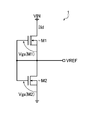
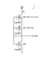
- FIG. 1 is a diagram showing a comparative example of a constant voltage generation circuit (an example of a basic configuration to be compared with the embodiment described later).
- the constant voltage generation circuit 1 of this comparative example is a so-called ED type reference voltage source, and has a depletion type N channel MOS field effect transistor M1 and an enhancement type N channel MOS field effect transistor M2.
- the depletion type refers to a type in which drain current flows even if the gate-source voltage is 0V.
- the enhancement type refers to a type in which drain current does not flow when the gate-source voltage is 0V.
- the drain of the transistor M1 is connected to the application end of the input voltage VIN (for example, 5V).
- the gate, source and back gate of the transistor M1 and the gate and drain of the transistor M2 are all connected to the output end of the constant voltage VREF.
- the main cause of the output variation in the constant voltage generation circuit 1 is that the drain current Id greatly fluctuates due to the process variation of the on-threshold voltage Vth (M1).
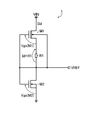
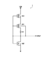
- FIG. 2 is a diagram showing a first embodiment of a constant voltage generation circuit.
- the constant voltage generation circuit 1 of the present embodiment is based on the above-mentioned comparative example (FIG. 1), and further has a resistor R1.
- the first end of the resistor R1 is connected to the source of the transistor M1.
- the second end of the resistor R1 is connected to the output end of the constant voltage VREF together with the gate and the back gate of the transistor M1. In this way, the resistor R1 is connected between the gate and the source of the transistor M1 and between the back gate and the source of the transistor M1.
- the resistor R1 for example, it is desirable to use a base resistor having a positive temperature characteristic.
- the type of the resistor R1 is not limited to this, and for example, a polyresistor having a negative temperature characteristic may be used as the resistor R1.
- FIG. 3 is a diagram showing the effect of suppressing variation in the drain current Id by adding the resistor R1.
- the horizontal axis represents the gate-source voltage Vgs (M1) of the transistor M1, and the vertical axis represents the drain current Id flowing through the transistor M1.
- the on-threshold voltage Vth (M1) of the transistor M1 varies to the negative side and the drain current Id becomes larger, the source potential of the transistor M1 is raised higher, so that the gate-source voltage Vgs (M1) of the transistor M1 is raised. Is shifted to the more negative side. As a result, the on-resistance value of the transistor M1 becomes high, so that it is possible to suppress an increase in the drain current Id.
- the resistance value of the resistor R1 may be 100 k ⁇ or more and less than 1 M ⁇ (for example, 100 k ⁇ ).
- the shift amount of the gate-source voltage Vgs (M1) can be set to about -100 mV (a fluctuation value according to the drain current Id).
- the resistor R1 is connected between the source of the transistor M1 and the back gate. Therefore, a difference occurs between the source potential and the back gate potential of the transistor M1 according to the drain current Id, so that the so-called substrate bias effect works.
- the above-mentioned substrate bias effect is one of the device characteristics of the MOSFET, and when a voltage is applied between the source and the back gate, the depletion layer region of the MOSFET expands and the on-threshold voltage fluctuates. Refers to the phenomenon of
- the on-threshold voltage Vth (M1) of the transistor M1 varies to the negative side and the drain current Id becomes larger, the source potential of the transistor M1 is raised higher, so that the on-threshold voltage Vth (M1) of the transistor M1 is positive.
- the above-mentioned substrate bias effect works so as to shift to the side, in other words, to suppress the negative side variation of the on-threshold voltage Vth (M1).
- the on-resistance value of the transistor M1 becomes high, so that it is possible to suppress an increase in the drain current Id.
- the output accuracy of the constant voltage VREF is ⁇ 4 to 6%
- the output accuracy of the constant voltage VREF is ⁇ 4 to 6%. It improves to about ⁇ 1%.
- FIG. 4 is a diagram showing a second embodiment of the constant voltage generation circuit.
- the constant voltage generation circuit 1 of this embodiment is based on the first embodiment (FIG. 2) described above, and further includes an enhancement type N-channel MOS field effect transistor M4.
- the drain of the transistor M4 is connected to the application end of the input voltage VIN.
- the gate of the transistor M4 is connected to the gate and back gate of the transistor M1, the drain of the transistor M2, and the second end of the resistor R1.
- the source and back gate of the transistor M4 are connected to the output end of the constant voltage VREF.
- the transistor M4 functions as a source follower for increasing the current capacity of the constant voltage generation circuit 1.
- the gate and back gate of the transistor M1, the drain of the transistor M2, and the second end of the resistor R1 are directly connected to the output end of the constant voltage VREF.
- the second embodiment in the second embodiment (FIG. 4), it is connected to the output terminal of the constant voltage via the source follower.
- the transistor M4 employs an element having a current capacity larger than that of the transistors M1 and M2.
- FIG. 5 is a diagram showing a third embodiment of the constant voltage generation circuit.
- the constant voltage generation circuit 1 of this embodiment is based on the second embodiment (FIG. 4), but resistors R2 and R3 are added.
- the first end of the resistor R2 is connected to the output end of the constant voltage VREF.
- the second end of the resistor R2 and the first end of the resistor R3 are connected to the gate of the transistor M2.
- the second end of the resistor R3 is connected to the grounded end.
- the resistors R2 and R3 connected in this way function as a resistor voltage divider that divides the constant voltage VREF and applies it to the gate of the transistor M2.
- the gate of the transistor M2 was directly connected to the output end of the constant voltage VREF, whereas the third embodiment In the embodiment (FIG. 5), it is connected to a constant voltage output end via a resistor divider.
- resistors R2 and R3 may be added while the first embodiment (FIG. 2) is the basis.
- FIG. 6 is a diagram showing a fourth embodiment of the constant voltage generation circuit.
- the constant voltage generation circuit 1 of the present embodiment is based on the third embodiment (FIG. 5) described above, and instead of the transistor M4, the P-channel MOS field effect transistors M5 and M6 and the current source CS are used. Have.
- the source and back gate of each of the transistors M5 and M6 are connected to the application end of the input voltage VIN.
- the gate of the transistor M5 is connected to the gate and back gate of the transistor M1, the drain of the transistor M2, and the second end of the resistor R1.
- the gate of the transistor M6 is connected to the drain of the transistor M5 and the first end of the current source CS.
- the second end of the current source CS is connected to the ground end.
- the drain of the transistor M6 is connected to the output end of the constant voltage VREF.
- the transistors M5 and M6 and the current source CS connected in this way function as a source follower for increasing the current capacity of the constant voltage generation circuit 1.
- FIG. 7 is a diagram showing a fifth embodiment of the constant voltage generation circuit.
- the constant voltage generation circuit 1 of this embodiment is based on the third embodiment (FIG. 5), and has a depletion type N-channel MOS field effect transistor M7 instead of the enhancement type transistor M4.
- FIG. 8 is a diagram showing a sixth embodiment of the constant voltage generation circuit.
- the constant voltage generation circuit 1 of this embodiment has a configuration in which a resistor R1 is inserted between the gate and source of the transistor M1 forming the ED reference voltage source, as in the first to fifth embodiments described so far. Is transformed into a configuration in which the drain current Id is supplied to the transistor M2 via a current mirror formed by using the P-channel MOS field effect transistors M8 and M9.
- the source of the transistor M1 is connected to the first end of the resistor R1.
- the gate and back gate of the transistor M1 and the second end of the resistor R1 are all connected to the ground end.
- the source and back gate of each of the transistors M8 and M9 are connected to the application end of the input voltage VIN.
- the gates of the transistors M8 and M9 are connected to the drain of the transistor M8.
- the source of the transistor M2 is connected to the ground end.
- FIG. 9 is a diagram showing Vds (M1) -Id characteristics and VIN-VREF characteristics in the previous comparative example (FIG. 1).
- the transistor M1 functions as a constant current source for determining the drain current Id, and depends on the gate-source voltage Vgs (M2) of the transistor M2 through which the drain current Id flows.
- the constant voltage VREF is determined.
- the drain current Id is almost constant, so ideally the constant voltage VREF should be constant regardless of the input voltage VIN.
- the actual drain current Id is not completely constant as represented by Id ⁇ (1 + ⁇ ⁇ Vds), and has a Vds-dependent slope determined by the channel length modulation parameter ⁇ , albeit slightly.
- the above channel length modulation parameter ⁇ is a characteristic peculiar to the device and varies depending on the element size. Therefore, when the input voltage VIN (and thus the drain-source voltage Vds (M1)) fluctuates, the drain current Id flowing through the transistor M1 changes, and the constant voltage VREF may fluctuate.
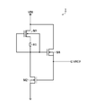
- FIG. 10 is a diagram showing a seventh embodiment of the constant voltage generation circuit.
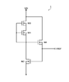
- the constant voltage generation circuit 1 of the present embodiment further includes a depletion type N-channel MOS field effect transistor M3 based on the above-mentioned comparative example (FIG. 1).
- the drain of the transistor M3 is connected to the application end of the input voltage VIN.
- the source and backgate of transistor M3 are connected to the drain of transistor M1.
- the gate of the transistor M3 is connected to the gate of the transistor M1. That is, the drain of the transistor M1 is connected to the application end of the input voltage VIN via the transistor M3.
- W / L of the transistor M1 is a and the W / L of the transistor M2 is b, it is desirable to design b to be about 20 to 100 times as large as a.
- FIG. 11 is a diagram showing the effect of reducing fluctuations in the drain current Id by adding the transistor M3.
- the horizontal axis represents the gate-source voltage Vgs, and the vertical axis represents the drain current Id.
- the drain current Id determined above also flows through the transistor M3.
- the clamp voltage at this time needs to be a voltage in the range where the transistor M1 becomes the saturation region, and it is necessary to consider the influence of the element characteristics and the size, but it is about 0.2 V or more.
- FIG. 12 is a diagram showing VIN-Vds (M1) characteristics in the seventh embodiment.
- FIG. 13 is a diagram showing an eighth embodiment of the constant voltage generation circuit.
- the constant voltage generation circuit 1 of this embodiment is based on the seventh embodiment (FIG. 10) described above, and further includes an enhancement type N-channel MOS field effect transistor M4.
- the drain of the transistor M4 is connected to the application end of the input voltage VIN.
- the gate of the transistor M4 is connected to the gate and back gate of the transistor M1, the drain of the transistor M2, and the gate of the transistor M3.
- the source and back gate of the transistor M4 are connected to the output end of the constant voltage VREF.
- the transistor M4 functions as a source follower for increasing the current capacity of the constant voltage generation circuit 1.
- the gate and back gate of the transistor M1, the drain of the transistor M2, and the gate of the transistor M3 are directly connected to the output end of the constant voltage VREF.
- the eighth embodiment (FIG. 13), it is connected to the output terminal of the constant voltage via the source follower.
- the transistor M4 employs an element having a current capacity larger than that of the transistors M1 and M2.
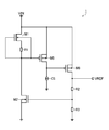
- FIG. 14 is a diagram showing a ninth embodiment of the constant voltage generation circuit.
- the constant voltage generation circuit 1 of this embodiment is based on the eighth embodiment (FIG. 13), but resistors R2 and R3 are added.
- the first end of the resistor R2 is connected to the output end of the constant voltage VREF.
- the second end of the resistor R2 and the first end of the resistor R3 are connected to the gate of the transistor M2.
- the second end of the resistor R3 is connected to the grounded end.
- the resistors R2 and R3 connected in this way function as a resistor voltage divider that divides the constant voltage VREF and applies it to the gate of the transistor M2.
- the gate of the transistor M2 is directly connected to the output end of the constant voltage VREF, whereas the ninth embodiment In the embodiment (FIG. 14), it is connected to a constant voltage output end via a resistor divider.
- resistors R2 and R3 may be added while the seventh embodiment (FIG. 10) is the basis.
- FIG. 15 is a diagram showing a tenth embodiment of a constant voltage generation circuit.
- the constant voltage generation circuit 1 of the present embodiment is based on the ninth embodiment (FIG. 14) described above, and instead of the transistor M4, the P-channel MOS field effect transistors M5 and M6 and the current source CS are used. Have.
- the source and back gate of each of the transistors M5 and M6 are connected to the application end of the input voltage VIN.
- the gate of the transistor M5 is connected to the gate and back gate of the transistor M1, the drain of the transistor M2, and the gate of the transistor M3.
- the gate of the transistor M6 is connected to the drain of the transistor M5 and the first end of the current source CS.
- the second end of the current source CS is connected to the ground end.
- the drain of the transistor M6 is connected to the output end of the constant voltage VREF.
- the transistors M5 and M6 and the current source CS connected in this way function as a source follower for increasing the current capacity of the constant voltage generation circuit 1.
- FIG. 16 is a diagram showing an eleventh embodiment of the constant voltage generation circuit.
- the constant voltage generation circuit 1 of the present embodiment is based on the ninth embodiment (FIG. 14), and has a depletion type N-channel MOS field effect transistor M7 instead of the enhancement type transistor M4.
- FIG. 17 is a diagram showing a twelfth embodiment of the constant voltage generation circuit.
- the constant voltage generation circuit 1 of the present embodiment has a configuration in which the transistor M3 is connected to the drain of the transistor M1 forming the ED reference voltage source, as in the seventh to eleventh embodiments described above.
- the configuration is modified to supply the drain current Id to the transistor M2 via a current mirror formed by using the channel MOS field effect transistors M8 and M9.
- the source and backgate of transistor M3 are connected to the drain of transistor M1. That is, the drain of the transistor M1 is connected to the input end of the current mirror via the transistor M3.
- the gate and back gate of the transistor M1 and the gate of the transistor M3 are connected to the ground end.
- the source and back gate of each of the transistors M8 and M9 are connected to the application end of the input voltage VIN.
- the gates of the transistors M8 and M9 are connected to the drain of the transistor M8.
- the source of the transistor M2 is connected to the ground end.
- FIG. 18 is a diagram showing a thirteenth embodiment of the constant voltage generation circuit.
- the constant voltage generation circuit 1 of the present embodiment is based on the seventh embodiment (FIG. 10) described above, and further has a resistor R1.
- the first end of the resistor R1 is connected to the source of the transistor M1.
- the second end of the resistor R1 is connected to the output end of the constant voltage VREF together with the gate and the back gate of the transistor M1. In this way, the resistor R1 is connected between the gate and the source of the transistor M1 and between the back gate and the source of the transistor M1.
- the seventh embodiment (FIG. 10) is used as the basis, but the resistor R1 may be inserted between the gate and source of the transistor M1 while using the eighth to twelfth embodiments as the basis. good.
- the constant voltage generation circuit disclosed in the present specification includes a depletion type first transistor and an enhancement type second transistor forming an ED type reference voltage source, and a gate and a source of the first transistor. It is configured to have a resistor connected between them (first configuration).
- the first transistor and the second transistor may be configured to be NMOSFETs (second configuration).
- the drain of the first transistor is connected to the application end of the input voltage, and the source of the second transistor is connected to the reference potential end.
- the gate of the first transistor and the drain of the second transistor are connected to the output end of a constant voltage directly or via a source follower, and the gate of the second transistor is directly or a resistance component.
- a configuration (third configuration) may be used in which the constant voltage output terminal is connected to the output end via a pressure device.
- the drain is connected to the application end of the input voltage and the gate is connected to the gate of the first transistor and the drain of the second transistor.
- the source may be configured to include an NMOSFET connected to the constant voltage output end (fourth configuration).
- the NMOSFET may have a depletion type configuration (fifth configuration).
- the source is connected to the application end of the input voltage and the gate is connected to the gate of the first transistor and the drain of the second transistor.
- the first PMOSFET, the second PMOSFET whose source is connected to the application end of the input voltage, the gate is connected to the drain of the first PMOSFET, and the drain is connected to the output end of the constant voltage, the drain of the first PMOSFET, and the drain of the first PMOSFET.
- the configuration may include a current source connected between the gate of the second PMOSFET and the reference potential end.
- the drain of the first transistor is connected to the input end of the current mirror, and the output end of the current mirror and the drain and gate of the second transistor are ,
- the gate of the first transistor and the source of the second transistor may be connected to the output end of the constant voltage (seventh configuration).
- the resistor may be a base resistor having a positive temperature characteristic (eighth configuration).
- the resistor may be a poly resistor having a negative temperature characteristic (nineth configuration).
- the drain current flowing through the first transistor is 100 nA or more and less than 1 ⁇ A
- the resistance value of the resistor is 100 k ⁇ or more and less than 1 M ⁇ . It may have a configuration (tenth configuration).
- another constant voltage generation circuit disclosed in the present specification includes a depletion type first transistor and an enhancement type second transistor forming an ED type reference voltage source, and a drain of the first transistor. It is configured to have a depletion type third transistor having a W / L larger than that of the first transistor, which is connected to the first transistor (11th configuration).
- the first transistor, the second transistor, and the third transistor may be configured to be NMOSFETs (12th configuration).
- the drain of the first transistor is connected to the application end of the input voltage via the third transistor, and the source of the second transistor is a reference. It is connected to the potential end, and the gates of the first transistor and the third transistor and the drain of the second transistor are connected to the output end of a constant voltage directly or via a source follower.
- the gate of the second transistor may be connected to the output end of the constant voltage directly or via a resistance voltage divider (thirteenth configuration).
- the drain is connected to the application end of the input voltage, and the gate is the gate of each of the first transistor and the third transistor and the second transistor.
- the configuration (14th configuration) may include an NMOSFET connected to the drain and the source connected to the output terminal of the constant voltage.
- the NMOSFET may have a depletion type configuration (15th configuration).
- the source is connected to the application end of the input voltage and the gate is the gate of each of the first transistor and the third transistor and the second.
- a first PMOSFET connected to the drain of a transistor, a second PMOSFET whose source is connected to the application end of the input voltage, a gate connected to the drain of the first PMOSFET, and a drain connected to the output end of the constant voltage.
- the configuration (16th configuration) may include a drain of the first PMOSFET and a current source connected between the gate of the second PMOSFET and the reference potential end.
- the drain of the first transistor is connected to the input end of the current mirror via the third transistor, and the output end of the current mirror and the first one.
- the drain and gate of the two transistors are connected to the output end of the constant voltage, and the gates of the first transistor and the third transistor and the source of the second transistor are connected to the reference potential end (a configuration in which the gates of the first transistor and the third transistor are connected to the reference potential end.
- the seventeenth configuration may be used.
- the constant voltage generation circuit having any of the 11th to 17th configurations may be configured to have a resistor connected between the gate and the source of the first transistor (18th configuration).
- the resistor may have a configuration (19th configuration) which is a base resistor having a positive temperature characteristic.
- the resistor may have a configuration (20th configuration) of a polyresistor having a negative temperature characteristic.
- the constant voltage generation circuit disclosed in the present specification can be suitably used, for example, as a means for generating a reference voltage or a threshold voltage inside a semiconductor device.
- Constant voltage generation circuit CS current source M1 NMOSFET (corresponds to the depletion type first transistor) M2 MOSFET (equivalent to an enhancement type second transistor) M3 MOSFET (equivalent to a depletion type third transistor) M4 MOSFET (enhancement type) M5, M6 MOSFET M7 MOSFET (depression type) M8, M9 MOSFET R1, R2, R3 resistors
Landscapes
- Engineering & Computer Science (AREA)
- Physics & Mathematics (AREA)
- Power Engineering (AREA)
- Electromagnetism (AREA)
- General Physics & Mathematics (AREA)
- Radar, Positioning & Navigation (AREA)
- Automation & Control Theory (AREA)
- Microelectronics & Electronic Packaging (AREA)
- Nonlinear Science (AREA)
- Control Of Electrical Variables (AREA)
Abstract
出力電圧精度の高い定電圧生成回路を提供する。 定電圧生成回路(1)は、ED型基準電圧源を形成するデプレッション型の第1トランジスタ(M1)及びエンハンスメント型の第2トランジスタ(M2)と、前記第1トランジスタ(M1)のゲートとソースとの間に接続された抵抗(R1)を有する。例えば、前記第1トランジスタ(M1)及び前記第2トランジスタ(M2)は、NMOSFETである。また、例えば、前記第1トランジスタ(M1)のドレインは、入力電圧(VIN)の印加端に接続されており、前記第2トランジスタ(M2)のソースは、基準電位端に接続されており、前記第1トランジスタ(M1)及び前記第2トランジスタ(M2)それぞれのゲート及び前記第2トランジスタ(M2)のドレインは、定電圧(VREF)の出力端に接続されている。
Description
本明細書中に開示されている発明は、定電圧生成回路に関する。
従来、定電圧生成回路の一種として、デプレッション型NMOSFET[metal oxide semiconductor field effect transistor]とエンハンスメント型NMOSFETを組み合わせたED型定電圧源が広く一般に知られている(例えば特許文献1を参照)。
しかしながら、上記従来の定電圧生成回路では、出力精度を向上する余地があった。
本明細書中に開示されている発明は、本願の発明者により見出された上記課題に鑑み、出力精度の高い定電圧生成回路を提供することを目的とする。
例えば、本明細書中に開示されている定電圧生成回路は、ED型基準電圧源を形成するデプレッション型の第1トランジスタ及びエンハンスメント型の第2トランジスタと、前記第1トランジスタのゲートとソースとの間に接続された抵抗と、を有する。
また、例えば、本明細書中に開示されている定電圧生成回路は、ED型基準電圧源を形成するデプレッション型の第1トランジスタ及びエンハンスメント型の第2トランジスタと、前記第1トランジスタのドレインに接続されて前記第1トランジスタよりもW/Lの大きいデプレッション型の第3トランジスタと、を有する。
なお、本発明のその他の特徴、要素、ステップ、利点、及び、特性については、以下に続く実施形態の詳細な説明やこれに関する添付の図面によって、さらに明らかとなる。
本明細書中に開示されている発明によれば、出力精度の高い定電圧生成回路を提供することが可能となる。
<比較例>
図1は、定電圧生成回路の比較例(後出の実施形態と対比される基本構成の一例)を示す図である。本比較例の定電圧生成回路1は、いわゆるED型基準電圧源であり、デプレッション型のNチャネルMOS電界効果トランジスタM1と、エンハンスメント型のNチャネルMOS電界効果トランジスタM2と、を有する。
図1は、定電圧生成回路の比較例(後出の実施形態と対比される基本構成の一例)を示す図である。本比較例の定電圧生成回路1は、いわゆるED型基準電圧源であり、デプレッション型のNチャネルMOS電界効果トランジスタM1と、エンハンスメント型のNチャネルMOS電界効果トランジスタM2と、を有する。
なお、デプレッション型とは、ゲート・ソース間電圧が0Vであってもドレイン電流が流れるものを指す。一方、エンハンスメント型とは、ゲート・ソース間電圧が0Vであるときにはドレイン電流が流れないものを指す。
トランジスタM1のドレインは、入力電圧VIN(例えば5V)の印加端に接続されている。トランジスタM2のソース及びバックゲートは、接地端(=基準電位端)に接続されている。トランジスタM1のゲート、ソース及びバックゲート、並びに、トランジスタM2のゲート及びドレインは、いずれも定電圧VREFの出力端に接続されている。
本比較例の定電圧生成回路1では、トランジスタM1のゲートとソースとの間が短絡されているので、トランジスタM1のゲート・ソース間電圧Vgs(M1)は0Vである。従って、トランジスタM1が一定のドレイン電流Idを生成する定電流源として機能し、トランジスタM2に一定のバイアス電流(=トランジスタM1のドレイン電流Id)が流れる。その結果、トランジスタM2のゲート・ソース間電圧Vgs(M2)に相当する一定の定電圧VREFが生成される。
<プロセスばらつきに関する考察>
ところで、トランジスタM1のオン閾値電圧Vth(M1)は、プロセスばらつきの影響を受け易いことが知られている。例えば、オン閾値電圧Vth(M1)が負側にばらつくと、ドレイン電流Idが標準値Id0よりも大きくなってしまうので、定電圧VREFが所望値から外れてしまう。
ところで、トランジスタM1のオン閾値電圧Vth(M1)は、プロセスばらつきの影響を受け易いことが知られている。例えば、オン閾値電圧Vth(M1)が負側にばらつくと、ドレイン電流Idが標準値Id0よりも大きくなってしまうので、定電圧VREFが所望値から外れてしまう。
このように、定電圧生成回路1における出力ばらつきの主な要因は、オン閾値電圧Vth(M1)のプロセスばらつきに起因して、ドレイン電流Idが大きく変動してしまうためである。
以下では、上記の考察に鑑み、プロセスばらつきに起因するドレイン電流Idの変動を抑えて、定電圧VREFの出力精度を向上することのできる新規な実施形態を提案する。
<第1実施形態>
図2は、定電圧生成回路の第1実施形態を示す図である。本実施形態の定電圧生成回路1は、先出の比較例(図1)を基本としつつ、抵抗R1をさらに有する。
図2は、定電圧生成回路の第1実施形態を示す図である。本実施形態の定電圧生成回路1は、先出の比較例(図1)を基本としつつ、抵抗R1をさらに有する。
抵抗R1の第1端は、トランジスタM1のソースに接続されている。抵抗R1の第2端は、トランジスタM1のゲート及びバックゲートとともに定電圧VREFの出力端に接続されている。このように、抵抗R1は、トランジスタM1のゲートとソースとの間、並びに、トランジスタM1のバックゲートとソースとの間に接続されている。
なお、抵抗R1としては、例えば、正の温度特性を持つベース抵抗を用いることが望ましい。ただし、抵抗R1の種類については、これに限定されるものではなく、例えば、抵抗R1として負の温度特性を持つポリ抵抗を用いてもよい。
図3は、抵抗R1の追加によるドレイン電流Idのばらつき抑制効果を示す図である。なお、横軸はトランジスタM1のゲート・ソース間電圧Vgs(M1)を示しており、縦軸はトランジスタM1に流れるドレイン電流Idを示している。
仮に、抵抗R1が設けられていない場合(先出の比較例に相当)には、トランジスタM1のゲート・ソース間電圧Vgs(M1)が0Vである。従って、トランジスタM1のオン閾値電圧Vth(M1)が負側にばらつくと、トランジスタM1に流れるドレイン電流Idが標準値Id0よりも大きくなってしまう(Id=Id0→Id1)。
一方、トランジスタM1のソースに抵抗R1が接続されている場合(第1実施形態に相当)には、抵抗R1の両端間にドレイン電流Idに応じた電位差(=Id×R1)が発生する。従って、トランジスタM1のゲート・ソース間電圧Vgs(M1)が負側にシフトされる(Vgs(M1)=-Id×R1)。
すなわち、トランジスタM1のオン閾値電圧Vth(M1)が負側にばらついて、ドレイン電流Idが大きくなるほど、トランジスタM1のソース電位がより高く持ち上げられるので、トランジスタM1のゲート・ソース間電圧Vgs(M1)がより負側にシフトされる。その結果、トランジスタM1のオン抵抗値が高くなるので、ドレイン電流Idの増大を抑制することが可能となる。
なお、トランジスタM1に流れるドレイン電流Idが100nA以上1μA未満(例えば100nA)である場合には、例えば、抵抗R1の抵抗値を100kΩ以上1MΩ未満(例えば100kΩ)とすればよい。このような素子設計を行うことにより、ゲート・ソース間電圧Vgs(M1)のシフト量を-100mV程度(ドレイン電流Idに応じた変動値)に設定することができる。
また、抵抗R1は、トランジスタM1のソースとバックゲートとの間に接続されているとも言える。そのため、ドレイン電流Idに応じて、トランジスタM1のソース電位とバックゲート電位との間にも差が生じるので、いわゆる基板バイアス効果が働く。
なお、上記の基板バイアス効果とは、MOSFETが持つデバイス特性の一つであり、ソースとバックゲートとの間に電圧が印加されることで、MOSFETの空乏層領域が広がり、オン閾値電圧が変動する現象を指す。
例えば、トランジスタM1のオン閾値電圧Vth(M1)が負側にばらついて、ドレイン電流Idが大きくなるほど、トランジスタM1のソース電位がより高く持ち上げられるので、トランジスタM1のオン閾値電圧Vth(M1)を正側にシフトするように、言い換えれば、オン閾値電圧Vth(M1)の負側ばらつきを抑えるように、上記の基板バイアス効果が働く。その結果、トランジスタM1のオン抵抗値が高くなるので、ドレイン電流Idの増大を抑制することが可能となる。
このように、本実施形態の定電圧生成回路1では、ドレイン電流Idが増大すると、抵抗R1の挿入によるゲート・ソース間電圧Vgs(M1)の負側シフト効果とオン閾値電圧Vth(M1)の正側シフト効果(=基板バイアス効果)が共に働くので、ドレイン電流Idの増大を抑えて(Id=Id1→Id2)、定電圧VREFの出力精度を向上し、さらには温度特性を改善することが可能となる。
例えば、抵抗R1が設けられていない場合には、定電圧VREFの出力精度が±4~6%であるのに対して、抵抗R1が設けられている場合には、定電圧VREFの出力精度が±1%程度まで向上する。
一方、ドレイン電流Idが標準値Id0よりも小さくなる方向にばらついた場合には、抵抗R1の両端間電圧が殆ど発生しなくなる。そのため、上記したゲート・ソース間電圧Vgs(M1)の負側シフト効果、及び、オン閾値電圧Vth(M1)の正側シフト効果(=基板バイアス効果)がいずれも働かなくなるので、抵抗R1の追加による影響はほぼなくなる。
<第2実施形態>
図4は、定電圧生成回路の第2実施形態を示す図である。本実施形態の定電圧生成回路1は、先出の第1実施形態(図2)を基本としつつ、エンハンスメント型のNチャネルMOS電界効果トランジスタM4をさらに有する。
図4は、定電圧生成回路の第2実施形態を示す図である。本実施形態の定電圧生成回路1は、先出の第1実施形態(図2)を基本としつつ、エンハンスメント型のNチャネルMOS電界効果トランジスタM4をさらに有する。
トランジスタM4のドレインは、入力電圧VINの印加端に接続されている。トランジスタM4のゲートは、トランジスタM1のゲート及びバックゲート、トランジスタM2のドレイン、並びに、抵抗R1の第2端に接続されている。トランジスタM4のソースとバックゲートは、定電圧VREFの出力端に接続されている。なお、トランジスタM4は、定電圧生成回路1の電流能力を高めるためのソースフォロワとして機能する。
すなわち、先出の第1実施形態(図2)では、トランジスタM1のゲート及びバックゲート、トランジスタM2のドレイン、並びに、抵抗R1の第2端が直接的に定電圧VREFの出力端に接続されていたのに対して、第2実施形態(図4)では、ソースフォロワを介して定電圧の出力端に接続されている。
このような構成であれば、ED基準電圧源(トランジスタM1及びM2)の温度特性に影響を及ぼすことなく、定電圧生成回路1の電流能力を高めることが可能となる。なお、当然のことながら、トランジスタM4としては、トランジスタM1及びM2よりも大きい電流能力を備えた素子を採用することが望ましい。
<第3実施形態>
図5は、定電圧生成回路の第3実施形態を示す図である。本実施形態の定電圧生成回路1は、先の第2実施形態(図4)を基本としつつ、抵抗R2及びR3が追加されている。
図5は、定電圧生成回路の第3実施形態を示す図である。本実施形態の定電圧生成回路1は、先の第2実施形態(図4)を基本としつつ、抵抗R2及びR3が追加されている。
抵抗R2の第1端は、定電圧VREFの出力端に接続されている。抵抗R2の第2端及び抵抗R3の第1端は、トランジスタM2のゲートに接続されている。抵抗R3の第2端は、接地端に接続されている。このように接続された抵抗R2及びR3は、定電圧VREFを分圧してトランジスタM2のゲートに印加する抵抗分圧器として機能する。
すなわち、先出の第1実施形態(図2)及び第2実施形態(図4)では、トランジスタM2のゲートが直接的に定電圧VREFの出力端に接続されていたのに対して、第3実施形態(図5)では、抵抗分圧器を介して定電圧の出力端に接続されている。
このような構成であれば、先の第1実施形態(図2)及び第2実施形態(図4)よりも高い定電圧VREF(=Vgs(M2)×{(R2+R3)/R3})を生成することが可能となる。
なお、本実施形態では、第2実施形態(図4)を基本としたが、第1実施形態(図2)を基本としつつ、抵抗R2及びR3を追加してもよい。
<第4実施形態>
図6は、定電圧生成回路の第4実施形態を示す図である。本実施形態の定電圧生成回路1は、先出の第3実施形態(図5)を基本としつつ、トランジスタM4に代えて、PチャネルMOS電界効果トランジスタM5及びM6と、電流源CSと、を有する。
図6は、定電圧生成回路の第4実施形態を示す図である。本実施形態の定電圧生成回路1は、先出の第3実施形態(図5)を基本としつつ、トランジスタM4に代えて、PチャネルMOS電界効果トランジスタM5及びM6と、電流源CSと、を有する。
トランジスタM5及びM6それぞれのソース及びバックゲートは、いずれも入力電圧VINの印加端に接続されている。トランジスタM5のゲートは、トランジスタM1のゲート及びバックゲート、トランジスタM2のドレイン、並びに、抵抗R1の第2端に接続されている。トランジスタM6のゲートは、トランジスタM5のドレインと電流源CSの第1端に接続されている。電流源CSの第2端は、接地端に接続されている。トランジスタM6のドレインは、定電圧VREFの出力端に接続されている。このように接続されたトランジスタM5及びM6と電流源CSは、定電圧生成回路1の電流能力を高めるためのソースフォロワとして機能する。
このように、ソースフォロワとしてPMOSFETを用いた構成であれば、ソースフォロワとしてNMOSFETを用いた第2実施形態(図4)及び第3実施形態(図5)よりも入力電圧VINが低い状態(=VIN-VREFが小さい状態)から動作することが可能となる。特に、定電圧VREFの出力目標値が高いときには有効であると言える。
<第5実施形態>
図7は、定電圧生成回路の第5実施形態を示す図である。本実施形態の定電圧生成回路1は、先の第3実施形態(図5)を基本としつつ、エンハンスメント型のトランジスタM4に代えて、デプレッション型のNチャネルMOS電界効果トランジスタM7を有する。
図7は、定電圧生成回路の第5実施形態を示す図である。本実施形態の定電圧生成回路1は、先の第3実施形態(図5)を基本としつつ、エンハンスメント型のトランジスタM4に代えて、デプレッション型のNチャネルMOS電界効果トランジスタM7を有する。
このように、ソースフォロワとしてデプレッション型のNMOSFETを用いた構成であれば、入力電圧VINの投入直後から、定電圧VREFを入力電圧VINに追従して出力することが可能となる。
<第6実施形態>
図8は、定電圧生成回路の第6実施形態を示す図である。本実施形態の定電圧生成回路1は、これまでに説明してきた第1~第5実施形態と同じく、ED基準電圧源を形成するトランジスタM1のゲート・ソース間に抵抗R1を挿入した構成であるが、PチャネルMOS電界効果トランジスタM8及びM9を用いて形成されるカレントミラーを介してトランジスタM2にドレイン電流Idを供給する構成に変形されている。
図8は、定電圧生成回路の第6実施形態を示す図である。本実施形態の定電圧生成回路1は、これまでに説明してきた第1~第5実施形態と同じく、ED基準電圧源を形成するトランジスタM1のゲート・ソース間に抵抗R1を挿入した構成であるが、PチャネルMOS電界効果トランジスタM8及びM9を用いて形成されるカレントミラーを介してトランジスタM2にドレイン電流Idを供給する構成に変形されている。
トランジスタM1のドレインは、トランジスタM8のドレイン(=カレントミラーの入力端)に接続されている。トランジスタM1のソースは、抵抗R1の第1端に接続されている。トランジスタM1のゲート及びバックゲート、並びに、抵抗R1の第2端は、いずれも接地端に接続されている。
トランジスタM8及びM9それぞれのソース及びバックゲートは、入力電圧VINの印加端に接続されている。トランジスタM8及びM9それぞれのゲートは、トランジスタM8のドレインに接続されている。トランジスタM9のドレイン(=カレントミラーの出力端)並びにトランジスタM2のドレイン及びゲートは、定電圧VREFの出力端に接続されている。トランジスタM2のソースは、接地端に接続されている。
このように、トランジスタM1のドレイン電流Idをカレントミラー経由でトランジスタM2に供給する回路形式であっても、先に説明した抵抗R1の挿入効果を享受することが可能である。
<入力電圧特性に関する考察>
図9は、先の比較例(図1)におけるVds(M1)-Id特性及びVIN-VREF特性を示す図である。先にも述べたように、ED型基準電圧源では、トランジスタM1がドレイン電流Idを決定する定電流源として機能し、ドレイン電流Idが流れるトランジスタM2のゲート・ソース間電圧Vgs(M2)に応じて定電圧VREFが決定される。
図9は、先の比較例(図1)におけるVds(M1)-Id特性及びVIN-VREF特性を示す図である。先にも述べたように、ED型基準電圧源では、トランジスタM1がドレイン電流Idを決定する定電流源として機能し、ドレイン電流Idが流れるトランジスタM2のゲート・ソース間電圧Vgs(M2)に応じて定電圧VREFが決定される。
ここで、トランジスタM1が飽和領域で動作しているときには、ドレイン電流Idがほぼ一定となるので、理想的には定電圧VREFが入力電圧VINに依ることなく一定となるはずである。しかしながら、実際のドレイン電流Idは、Id∝(1+λ×Vds)で表されるように、完全に一定ではなく、若干ながらもチャネル長変調パラメータλで決定されるVds依存の傾きを持つ。
なお、上記のチャネル長変調パラメータλは、デバイス固有の特性であり、素子サイズによっても変動する。そのため、入力電圧VIN(延いてはドレイン・ソース間電圧Vds(M1))が変動すると、トランジスタM1に流れるドレイン電流Idが変化し、延いては、定電圧VREFが変動するおそれがあった。
以下では、上記の考察に鑑み、入力電圧変動に起因するドレイン電流Idの変動を抑えて、定電圧VREFの出力精度を向上することのできる新規な実施形態を提案する。
<第7実施形態>
図10は、定電圧生成回路の第7実施形態を示す図である。本実施形態の定電圧生成回路1は、先出の比較例(図1)を基本としつつ、デプレッション型のNチャネルMOS電界効果トランジスタM3をさらに有する。
図10は、定電圧生成回路の第7実施形態を示す図である。本実施形態の定電圧生成回路1は、先出の比較例(図1)を基本としつつ、デプレッション型のNチャネルMOS電界効果トランジスタM3をさらに有する。
トランジスタM3のドレインは、入力電圧VINの印加端に接続されている。トランジスタM3のソース及びバックゲートは、トランジスタM1のドレインに接続されている。トランジスタM3のゲートは、トランジスタM1のゲートに接続されている。すなわち、トランジスタM1のドレインは、トランジスタM3を介して入力電圧VINの印加端に接続されている。
なお、トランジスタM1を飽和領域で用いるためには、トランジスタM1のドレイン・ソース間電圧Vds(M1)を0.2V以上に設定する必要があり、そうなるようにトランジスタM3のサイズを決定する必要がある。そこで、トランジスタM3は、トランジスタM1よりも十分に大きいW/L(=チャネル幅Wとチャネル長Lとの比)を持つようにデバイス設計されている。例えば、トランジスタM1のW/Lをaとし、トランジスタM2のW/Lをbとした場合、bはaの20~100倍程度に設計することが望ましい。
図11は、トランジスタM3の追加によるドレイン電流Idの変動低減効果を示す図である。なお、横軸はゲート・ソース間電圧Vgsを示しており、縦軸はドレイン電流Idを示している。
先にも述べた通り、トランジスタM3のW/Lは、トランジスタM1のW/Lよりも十分大きい値に設計されている。従って、トランジスタM3のオン閾値電圧Vth(M3)は、トランジスタM1のオン閾値電圧Vth(M1)よりも十分小さくなる。その結果、ドレイン電流Idを決定する要素としては、トランジスタM3よりもトランジスタM1が支配的となる。すなわち、トランジスタM1によって決定されるドレイン電流をId(M1)とした場合、Id=Id(M1)が成立する。
また、トランジスタM1及びM3は、互いに直列接続されているので、上記で決定されたドレイン電流IdがトランジスタM3にも流れる。その結果、トランジスタM3は、ドレイン電流Id(M1)が流れる状態(Id=Id(M1)=Id(M3)となる状態)で安定する。すなわち、トランジスタM3は、ゲート・ソース間電圧Vgs(M3)として負電圧が発生した状態でクランプされる形となる。このときのクランプ電圧は、トランジスタM1が飽和領域になる範囲の電圧にする必要があり、素子特性やサイズの影響を考慮する必要もあるが、約0.2V以上となる。
図12は、第7実施形態におけるVIN-Vds(M1)特性を示す図である。上記一連の動作により、入力電圧VINが変動してもトランジスタM1のドレイン・ソース間電圧Vds(M1)がほぼ一定となる。従って、入力電圧変動に起因するドレイン電流Idの変動を抑えて、定電圧VREFの出力精度を向上することが可能となる。
<第8実施形態>
図13は、定電圧生成回路の第8実施形態を示す図である。本実施形態の定電圧生成回路1は、先出の第7実施形態(図10)を基本としつつ、エンハンスメント型のNチャネルMOS電界効果トランジスタM4をさらに有する。
図13は、定電圧生成回路の第8実施形態を示す図である。本実施形態の定電圧生成回路1は、先出の第7実施形態(図10)を基本としつつ、エンハンスメント型のNチャネルMOS電界効果トランジスタM4をさらに有する。
トランジスタM4のドレインは、入力電圧VINの印加端に接続されている。トランジスタM4のゲートは、トランジスタM1のゲート及びバックゲート、トランジスタM2のドレイン、並びに、トランジスタM3のゲートに接続されている。トランジスタM4のソースとバックゲートは、定電圧VREFの出力端に接続されている。なお、トランジスタM4は、定電圧生成回路1の電流能力を高めるためのソースフォロワとして機能する。
すなわち、先出の第7実施形態(図10)では、トランジスタM1のゲート及びバックゲート、トランジスタM2のドレイン、並びに、トランジスタM3のゲートが直接的に定電圧VREFの出力端に接続されていたのに対して、第8実施形態(図13)では、ソースフォロワを介して定電圧の出力端に接続されている。
このような構成であれば、ED基準電圧源(トランジスタM1及びM2)の温度特性に影響を及ぼすことなく、定電圧生成回路1の電流能力を高めることが可能となる。なお、当然のことながら、トランジスタM4としては、トランジスタM1及びM2よりも大きい電流能力を備えた素子を採用することが望ましい。
<第9実施形態>
図14は、定電圧生成回路の第9実施形態を示す図である。本実施形態の定電圧生成回路1は、第8実施形態(図13)を基本としつつ、抵抗R2及びR3が追加されている。
図14は、定電圧生成回路の第9実施形態を示す図である。本実施形態の定電圧生成回路1は、第8実施形態(図13)を基本としつつ、抵抗R2及びR3が追加されている。
抵抗R2の第1端は、定電圧VREFの出力端に接続されている。抵抗R2の第2端及び抵抗R3の第1端は、トランジスタM2のゲートに接続されている。抵抗R3の第2端は、接地端に接続されている。このように接続された抵抗R2及びR3は、定電圧VREFを分圧してトランジスタM2のゲートに印加する抵抗分圧器として機能する。
すなわち、先出の第7実施形態(図10)及び第8実施形態(図13)では、トランジスタM2のゲートが直接的に定電圧VREFの出力端に接続されていたのに対して、第9実施形態(図14)では、抵抗分圧器を介して定電圧の出力端に接続されている。
このような構成であれば、先の第7実施形態(図10)及び第8実施形態(図13)よりも高い定電圧VREF(=Vgs(M2)×{(R2+R3)/R3})を生成することが可能となる。
なお、本実施形態では、第8実施形態(図13)を基本としたが、第7実施形態(図10)を基本としつつ、抵抗R2及びR3を追加してもよい。
<第10実施形態>
図15は、定電圧生成回路の第10実施形態を示す図である。本実施形態の定電圧生成回路1は、先出の第9実施形態(図14)を基本としつつ、トランジスタM4に代えて、PチャネルMOS電界効果トランジスタM5及びM6と、電流源CSと、を有する。
図15は、定電圧生成回路の第10実施形態を示す図である。本実施形態の定電圧生成回路1は、先出の第9実施形態(図14)を基本としつつ、トランジスタM4に代えて、PチャネルMOS電界効果トランジスタM5及びM6と、電流源CSと、を有する。
トランジスタM5及びM6それぞれのソース及びバックゲートは、いずれも入力電圧VINの印加端に接続されている。トランジスタM5のゲートは、トランジスタM1のゲート及びバックゲート、トランジスタM2のドレイン、並びに、トランジスタM3のゲートに接続されている。トランジスタM6のゲートは、トランジスタM5のドレインと電流源CSの第1端に接続されている。電流源CSの第2端は、接地端に接続されている。トランジスタM6のドレインは、定電圧VREFの出力端に接続されている。このように接続されたトランジスタM5及びM6と電流源CSは、定電圧生成回路1の電流能力を高めるためのソースフォロワとして機能する。
このように、ソースフォロワとしてPMOSFETを用いた構成であれば、ソースフォロワとしてNMOSFETを用いた第8実施形態(図13)及び第9実施形態(図14)よりも入力電圧VINが低い状態(=VIN-VREFが小さい状態)から動作することが可能となる。特に、定電圧VREFの出力目標値が高いときには有効であると言える。
<第11実施形態>
図16は、定電圧生成回路の第11実施形態を示す図である。本実施形態の定電圧生成回路1は、第9実施形態(図14)を基本としつつ、エンハンスメント型のトランジスタM4に代えてデプレッション型のNチャネルMOS電界効果トランジスタM7を有する。
図16は、定電圧生成回路の第11実施形態を示す図である。本実施形態の定電圧生成回路1は、第9実施形態(図14)を基本としつつ、エンハンスメント型のトランジスタM4に代えてデプレッション型のNチャネルMOS電界効果トランジスタM7を有する。
このように、ソースフォロワとしてデプレッション型のNMOSFETを用いた構成であれば、入力電圧VINの投入直後から、定電圧VREFを入力電圧VINに追従して出力することが可能となる。
<第12実施形態>
図17は、定電圧生成回路の第12実施形態を示す図である。本実施形態の定電圧生成回路1は、これまでに説明してきた第7~第11実施形態と同じく、ED基準電圧源を形成するトランジスタM1のドレインにトランジスタM3を接続した構成であるが、PチャネルMOS電界効果トランジスタM8及びM9を用いて形成されるカレントミラーを介してトランジスタM2にドレイン電流Idを供給する構成に変形されている。
図17は、定電圧生成回路の第12実施形態を示す図である。本実施形態の定電圧生成回路1は、これまでに説明してきた第7~第11実施形態と同じく、ED基準電圧源を形成するトランジスタM1のドレインにトランジスタM3を接続した構成であるが、PチャネルMOS電界効果トランジスタM8及びM9を用いて形成されるカレントミラーを介してトランジスタM2にドレイン電流Idを供給する構成に変形されている。
トランジスタM3のドレインは、トランジスタM8のドレイン(=カレントミラーの入力端)に接続されている。トランジスタM3のソース及びバックゲートは、トランジスタM1のドレインに接続されている。すなわち、トランジスタM1のドレインは、トランジスタM3を介してカレントミラーの入力端に接続されている。トランジスタM1のゲート及びバックゲート、並びに、トランジスタM3のゲートは、接地端に接続されている。
トランジスタM8及びM9それぞれのソース及びバックゲートは、入力電圧VINの印加端に接続されている。トランジスタM8及びM9それぞれのゲートは、トランジスタM8のドレインに接続されている。トランジスタM9のドレイン(=カレントミラーの出力端)並びにトランジスタM2のドレイン及びゲートは、定電圧VREFの出力端に接続されている。トランジスタM2のソースは、接地端に接続されている。
このように、トランジスタM1のドレイン電流Idをカレントミラー経由でトランジスタM2に供給する回路形式であっても、先に説明したトランジスタM3の挿入効果を享受することが可能である。
<第13実施形態>
図18は、定電圧生成回路の第13実施形態を示す図である。本実施形態の定電圧生成回路1は、先出の第7実施形態(図10)を基本としつつ、抵抗R1をさらに有する。
図18は、定電圧生成回路の第13実施形態を示す図である。本実施形態の定電圧生成回路1は、先出の第7実施形態(図10)を基本としつつ、抵抗R1をさらに有する。
抵抗R1の第1端は、トランジスタM1のソースに接続されている。抵抗R1の第2端は、トランジスタM1のゲート及びバックゲートとともに定電圧VREFの出力端に接続されている。このように、抵抗R1は、トランジスタM1のゲートとソースとの間、並びに、トランジスタM1のバックゲートとソースとの間に接続されている。
本実施形態であれば、抵抗R1の挿入によるドレイン電流Idのばらつき抑制効果を享受することができる。従って、入力電圧変動に起因するドレイン電流Idの変動だけでなく、プロセスばらつきに起因するドレイン電流Idの変動も抑えることができるので、定電圧VREFの出力精度をさらに向上することが可能となる。
なお、本実施形態では、第7実施形態(図10)を基本としたが、第8~第12実施形態を基本としつつ、それぞれ、トランジスタM1のゲート・ソース間に抵抗R1を挿入してもよい。
<総括>
以下では、本明細書中に開示されている種々の実施形態について、総括的に述べる。
以下では、本明細書中に開示されている種々の実施形態について、総括的に述べる。
例えば、本明細書中に開示されている定電圧生成回路は、ED型基準電圧源を形成するデプレッション型の第1トランジスタ及びエンハンスメント型の第2トランジスタと、前記第1トランジスタのゲートとソースとの間に接続された抵抗と、を有する構成(第1の構成)とされている。
なお、上記第1の構成から成る定電圧生成回路において、前記第1トランジスタ及び前記第2トランジスタは、NMOSFETである構成(第2の構成)にしてもよい。
また、上記第2の構成から成る定電圧生成回路において、前記第1トランジスタのドレインは、入力電圧の印加端に接続されており、前記第2トランジスタのソースは、基準電位端に接続されており、前記第1トランジスタのゲート及び前記第2トランジスタのドレインは、直接的に若しくはソースフォロワを介して定電圧の出力端に接続されており、前記第2トランジスタのゲートは、直接的に若しくは抵抗分圧器を介して前記定電圧の出力端に接続されている構成(第3の構成)にしてもよい。
また、上記第3の構成から成る定電圧生成回路において、前記ソースフォロワは、ドレインが前記入力電圧の印加端に接続されてゲートが前記第1トランジスタのゲート及び前記第2トランジスタのドレインに接続されてソースが前記定電圧の出力端に接続されたNMOSFETを含む構成(第4の構成)にしてもよい。
また、上記第4の構成から成る定電圧生成回路において、前記NMOSFETは、デプレッション型である構成(第5の構成)にしてもよい。
また、上記第3の構成から成る定電圧生成回路において、前記ソースフォロワは、ソースが前記入力電圧の印加端に接続されてゲートが前記第1トランジスタのゲート及び前記第2トランジスタのドレインに接続された第1PMOSFETと、ソースが前記入力電圧の印加端に接続されてゲートが前記第1PMOSFETのドレインに接続されてドレインが前記定電圧の出力端に接続された第2PMOSFETと、記第1PMOSFETのドレイン及び前記第2PMOSFETのゲートと前記基準電位端との間に接続された電流源とを含む構成(第6の構成)にしてもよい。
また、上記第2の構成から成る定電圧生成回路において、前記第1トランジスタのドレインは、カレントミラーの入力端に接続されており、前記カレントミラーの出力端並びに前記第2トランジスタのドレイン及びゲートは、定電圧の出力端に接続されており、前記第1トランジスタのゲート及び前記第2トランジスタのソースは、基準電位端に接続されている構成(第7の構成)にしてもよい。
また、上記第1~第7いずれかの構成から成る定電圧生成回路において、前記抵抗は、正の温度特性を持つベース抵抗である構成(第8の構成)にしてもよい。
また、上記第1~第7いずれかの構成から成る定電圧生成回路において、前記抵抗は、負の温度特性を持つポリ抵抗である構成(第9の構成)にしてもよい。
また、上記第1~第9いずれかの構成から成る定電圧生成回路において、前記第1トランジスタに流れるドレイン電流は、100nA以上1μA未満であり、前記抵抗の抵抗値は、100kΩ以上1MΩ未満である構成(第10の構成)にしてもよい。
また、例えば、本明細書中に開示されている別の定電圧生成回路は、ED型基準電圧源を形成するデプレッション型の第1トランジスタ及びエンハンスメント型の第2トランジスタと、前記第1トランジスタのドレインに接続されて前記第1トランジスタよりもW/Lの大きいデプレッション型の第3トランジスタと、を有する構成(第11の構成)とされている。
なお、上記第11の構成から成る定電圧生成回路において、前記第1トランジスタ、前記第2トランジスタ、及び、前記第3トランジスタは、NMOSFETである構成(第12の構成)にしてもよい。
また、上記第12の構成から成る定電圧生成回路において、前記第1トランジスタのドレインは、前記第3トランジスタを介して入力電圧の印加端に接続されており、前記第2トランジスタのソースは、基準電位端に接続されており、前記第1トランジスタ及び前記第3トランジスタそれぞれのゲート及び前記第2トランジスタのドレインは、直接的に若しくはソースフォロワを介して定電圧の出力端に接続されており、前記第2トランジスタのゲートは、直接的に若しくは抵抗分圧器を介して前記定電圧の出力端に接続されている構成(第13の構成)にしてもよい。
上記第13の構成から成る定電圧生成回路において、前記ソースフォロワは、ドレインが前記入力電圧の印加端に接続されてゲートが前記第1トランジスタ及び前記第3トランジスタそれぞれのゲート及び前記第2トランジスタのドレインに接続されてソースが前記定電圧の出力端に接続されたNMOSFETを含む構成(第14の構成)にしてもよい。
また、上記第14の構成から成る定電圧生成回路において、前記NMOSFETは、デプレッション型である構成(第15の構成)にしてもよい。
また、上記第13の構成から成る定電圧生成回路において、前記ソースフォロワは、ソースが前記入力電圧の印加端に接続されてゲートが前記第1トランジスタ及び前記第3トランジスタそれぞれのゲート及び前記第2トランジスタのドレインに接続された第1PMOSFETと、ソースが前記入力電圧の印加端に接続されてゲートが前記第1PMOSFETのドレインに接続されてドレインが前記定電圧の出力端に接続された第2PMOSFETと、記第1PMOSFETのドレイン及び前記第2PMOSFETのゲートと前記基準電位端との間に接続された電流源と、を含む構成(第16の構成)にしてもよい。
また、上記第12の構成から成る定電圧生成回路において、前記第1トランジスタのドレインは、前記第3トランジスタを介してカレントミラーの入力端に接続されており、前記カレントミラーの出力端並びに前記第2トランジスタのドレイン及びゲートは、定電圧の出力端に接続されており、前記第1トランジスタ及び前記第3トランジスタそれぞれのゲート及び前記第2トランジスタのソースは、基準電位端に接続されている構成(第17の構成)にしてもよい。
上記第11~第17いずれかの構成から成る定電圧生成回路は、前記第1トランジスタのゲートとソースとの間に接続された抵抗を有する構成(第18の構成)にしてもよい。
また、上記第18の構成から成る定電圧生成回路において、前記抵抗は、正の温度特性を持つベース抵抗である構成(第19の構成)にしてもよい。
また、上記第18の構成から成る定電圧生成回路において、前記抵抗は、負の温度特性を持つポリ抵抗である構成(第20の構成)にしてもよい。
<その他の変形例>
なお、本明細書中に開示されている種々の技術的特徴は、上記実施形態のほか、その技術的創作の主旨を逸脱しない範囲で種々の変更を加えることが可能である。すなわち、上記実施形態は、全ての点で例示であって制限的なものではないと考えられるべきであり、本発明の技術的範囲は、上記実施形態に限定されるものではなく、特許請求の範囲と均等の意味及び範囲内に属する全ての変更が含まれると理解されるべきである。
なお、本明細書中に開示されている種々の技術的特徴は、上記実施形態のほか、その技術的創作の主旨を逸脱しない範囲で種々の変更を加えることが可能である。すなわち、上記実施形態は、全ての点で例示であって制限的なものではないと考えられるべきであり、本発明の技術的範囲は、上記実施形態に限定されるものではなく、特許請求の範囲と均等の意味及び範囲内に属する全ての変更が含まれると理解されるべきである。
本明細書中に開示されている定電圧生成回路は、例えば、半導体装置内部における参照電圧や閾値電圧を生成する手段として、好適に利用することが可能である。
1 定電圧生成回路
CS 電流源
M1 NMOSFET(デプレッション型の第1トランジスタに相当)
M2 NMOSFET(エンハンスメント型の第2トランジスタに相当)
M3 NMOSFET(デプレッション型の第3トランジスタに相当)
M4 NMOSFET(エンハンスメント型)
M5、M6 PMOSFET
M7 NMOSFET(デプレッション型)
M8、M9 PMOSFET
R1、R2、R3 抵抗
CS 電流源
M1 NMOSFET(デプレッション型の第1トランジスタに相当)
M2 NMOSFET(エンハンスメント型の第2トランジスタに相当)
M3 NMOSFET(デプレッション型の第3トランジスタに相当)
M4 NMOSFET(エンハンスメント型)
M5、M6 PMOSFET
M7 NMOSFET(デプレッション型)
M8、M9 PMOSFET
R1、R2、R3 抵抗
Claims (20)
- ED型基準電圧源を形成するデプレッション型の第1トランジスタ及びエンハンスメント型の第2トランジスタと、
前記第1トランジスタのゲートとソースとの間に接続された抵抗と、
を有する、定電圧生成回路。 - 前記第1トランジスタ及び前記第2トランジスタは、NMOSFETである、請求項1に記載の定電圧生成回路。
- 前記第1トランジスタのドレインは、入力電圧の印加端に接続されており、
前記第2トランジスタのソースは、基準電位端に接続されており、
前記第1トランジスタのゲート及び前記第2トランジスタのドレインは、直接的に若しくはソースフォロワを介して定電圧の出力端に接続されており、
前記第2トランジスタのゲートは、直接的に若しくは抵抗分圧器を介して前記定電圧の出力端に接続されている、
請求項2に記載の定電圧生成回路。 - 前記ソースフォロワは、ドレインが前記入力電圧の印加端に接続されてゲートが前記第1トランジスタのゲート及び前記第2トランジスタのドレインに接続されてソースが前記定電圧の出力端に接続されたNMOSFETを含む、請求項3に記載の定電圧生成回路。
- 前記NMOSFETは、デプレッション型である、請求項4に記載の定電圧生成回路。
- 前記ソースフォロワは、
ソースが前記入力電圧の印加端に接続されてゲートが前記第1トランジスタのゲート及び前記第2トランジスタのドレインに接続された第1PMOSFETと、
ソースが前記入力電圧の印加端に接続されてゲートが前記第1PMOSFETのドレインに接続されてドレインが前記定電圧の出力端に接続された第2PMOSFETと、
記第1PMOSFETのドレイン及び前記第2PMOSFETのゲートと前記基準電位端との間に接続された電流源と、
を含む、請求項3に記載の定電圧生成回路。 - 前記第1トランジスタのドレインは、カレントミラーの入力端に接続されており、
前記カレントミラーの出力端並びに前記第2トランジスタのドレイン及びゲートは、定電圧の出力端に接続されており、
前記第1トランジスタのゲート及び前記第2トランジスタのソースは、基準電位端に接続されている、
請求項2に記載の定電圧生成回路。 - 前記抵抗は、正の温度特性を持つベース抵抗である、請求項1~7のいずれか一項に記載の定電圧生成回路。
- 前記抵抗は、負の温度特性を持つポリ抵抗である、請求項1~7のいずれか一項に記載の定電圧生成回路。
- 前記第1トランジスタに流れるドレイン電流は、100nA以上1μA未満であり、
前記抵抗の抵抗値は、100kΩ以上1MΩ未満である、
請求項1~9のいずれか一項に記載の定電圧生成回路。 - ED型基準電圧源を形成するデプレッション型の第1トランジスタ及びエンハンスメント型の第2トランジスタと、
前記第1トランジスタのドレインに接続されて前記第1トランジスタよりもW/Lの大きいデプレッション型の第3トランジスタと、
を有する、定電圧生成回路。 - 前記第1トランジスタ、前記第2トランジスタ、及び、前記第3トランジスタは、NMOSFETである、請求項11に記載の定電圧生成回路。
- 前記第1トランジスタのドレインは、前記第3トランジスタを介して入力電圧の印加端に接続されており、
前記第2トランジスタのソースは、基準電位端に接続されており、
前記第1トランジスタ及び前記第3トランジスタそれぞれのゲート及び前記第2トランジスタのドレインは、直接的に若しくはソースフォロワを介して定電圧の出力端に接続されており、
前記第2トランジスタのゲートは、直接的に若しくは抵抗分圧器を介して前記定電圧の出力端に接続されている、
請求項12に記載の定電圧生成回路。 - 前記ソースフォロワは、ドレインが前記入力電圧の印加端に接続されてゲートが前記第1トランジスタ及び前記第3トランジスタそれぞれのゲート及び前記第2トランジスタのドレインに接続されてソースが前記定電圧の出力端に接続されたNMOSFETを含む、請求項13に記載の定電圧生成回路。
- 前記NMOSFETは、デプレッション型である、請求項14に記載の定電圧生成回路。
- 前記ソースフォロワは、
ソースが前記入力電圧の印加端に接続されてゲートが前記第1トランジスタ及び前記第3トランジスタそれぞれのゲート及び前記第2トランジスタのドレインに接続された第1PMOSFETと、
ソースが前記入力電圧の印加端に接続されてゲートが前記第1PMOSFETのドレインに接続されてドレインが前記定電圧の出力端に接続された第2PMOSFETと、
記第1PMOSFETのドレイン及び前記第2PMOSFETのゲートと前記基準電位端との間に接続された電流源と、
を含む、請求項13に記載の定電圧生成回路。 - 前記第1トランジスタのドレインは、前記第3トランジスタを介してカレントミラーの入力端に接続されており、
前記カレントミラーの出力端並びに前記第2トランジスタのドレイン及びゲートは、定電圧の出力端に接続されており、
前記第1トランジスタ及び前記第3トランジスタそれぞれのゲート及び前記第2トランジスタのソースは、基準電位端に接続されている、
請求項12に記載の定電圧生成回路。 - 前記第1トランジスタのゲートとソースとの間に接続された抵抗をさらに有する、請求項11~17のいずれか一項に記載の定電圧生成回路。
- 前記抵抗は正の温度特性を持つベース抵抗である、請求項18に記載の定電圧生成回路。
- 前記抵抗は負の温度特性を持つポリ抵抗である、請求項18に記載の定電圧生成回路。
Priority Applications (4)
| Application Number | Priority Date | Filing Date | Title |
|---|---|---|---|
| US17/798,619 US20230135542A1 (en) | 2020-02-25 | 2021-02-09 | Constant voltage generation circuit |
| DE112021001229.0T DE112021001229T5 (de) | 2020-02-25 | 2021-02-09 | Konstantspannung-Erzeugungsschaltung |
| JP2022503239A JPWO2021172001A1 (ja) | 2020-02-25 | 2021-02-09 | |
| CN202180014654.8A CN115104076A (zh) | 2020-02-25 | 2021-02-09 | 恒定电压生成电路 |
Applications Claiming Priority (4)
| Application Number | Priority Date | Filing Date | Title |
|---|---|---|---|
| JP2020029233 | 2020-02-25 | ||
| JP2020-029233 | 2020-02-25 | ||
| JP2020-029235 | 2020-02-25 | ||
| JP2020029235 | 2020-02-25 |
Publications (1)
| Publication Number | Publication Date |
|---|---|
| WO2021172001A1 true WO2021172001A1 (ja) | 2021-09-02 |
Family
ID=77490491
Family Applications (1)
| Application Number | Title | Priority Date | Filing Date |
|---|---|---|---|
| PCT/JP2021/004749 Ceased WO2021172001A1 (ja) | 2020-02-25 | 2021-02-09 | 定電圧生成回路 |
Country Status (5)
| Country | Link |
|---|---|
| US (1) | US20230135542A1 (ja) |
| JP (1) | JPWO2021172001A1 (ja) |
| CN (1) | CN115104076A (ja) |
| DE (1) | DE112021001229T5 (ja) |
| WO (1) | WO2021172001A1 (ja) |
Cited By (1)
| Publication number | Priority date | Publication date | Assignee | Title |
|---|---|---|---|---|
| CN115037150A (zh) * | 2022-06-10 | 2022-09-09 | 西安博瑞集信电子科技有限公司 | 一种用于砷化镓电路的稳压电路和采用其的射频电路 |
Families Citing this family (2)
| Publication number | Priority date | Publication date | Assignee | Title |
|---|---|---|---|---|
| EP4435554A1 (en) * | 2023-03-24 | 2024-09-25 | Nexperia B.V. | Reference voltage circuit |
| IT202300006477A1 (it) * | 2023-04-03 | 2024-10-03 | Circuito di regolazione di tensione |
Citations (3)
| Publication number | Priority date | Publication date | Assignee | Title |
|---|---|---|---|---|
| JPH11194844A (ja) * | 1998-01-05 | 1999-07-21 | Seiko Instruments Inc | 自己補正型定電流回路 |
| JP2011113321A (ja) * | 2009-11-26 | 2011-06-09 | Torex Semiconductor Ltd | 基準電圧回路 |
| CN107153442A (zh) * | 2016-03-02 | 2017-09-12 | 上海南麟电子股份有限公司 | 一种带阻抗调节的耗尽管基准电路 |
Family Cites Families (5)
| Publication number | Priority date | Publication date | Assignee | Title |
|---|---|---|---|---|
| JPS60182219A (ja) * | 1984-02-29 | 1985-09-17 | Fujitsu Ltd | 半導体装置 |
| US4645948A (en) * | 1984-10-01 | 1987-02-24 | At&T Bell Laboratories | Field effect transistor current source |
| US4853646A (en) * | 1988-07-19 | 1989-08-01 | Fairchild Semiconductor Corporation | Temperature compensated bipolar circuits |
| US6424205B1 (en) * | 2000-08-07 | 2002-07-23 | Semiconductor Components Industries Llc | Low voltage ACMOS reference with improved PSRR |
| CN104793689A (zh) * | 2015-04-10 | 2015-07-22 | 无锡中星微电子有限公司 | 基准电压源电路 |
-
2021
- 2021-02-09 CN CN202180014654.8A patent/CN115104076A/zh active Pending
- 2021-02-09 JP JP2022503239A patent/JPWO2021172001A1/ja active Pending
- 2021-02-09 WO PCT/JP2021/004749 patent/WO2021172001A1/ja not_active Ceased
- 2021-02-09 DE DE112021001229.0T patent/DE112021001229T5/de active Pending
- 2021-02-09 US US17/798,619 patent/US20230135542A1/en not_active Abandoned
Patent Citations (3)
| Publication number | Priority date | Publication date | Assignee | Title |
|---|---|---|---|---|
| JPH11194844A (ja) * | 1998-01-05 | 1999-07-21 | Seiko Instruments Inc | 自己補正型定電流回路 |
| JP2011113321A (ja) * | 2009-11-26 | 2011-06-09 | Torex Semiconductor Ltd | 基準電圧回路 |
| CN107153442A (zh) * | 2016-03-02 | 2017-09-12 | 上海南麟电子股份有限公司 | 一种带阻抗调节的耗尽管基准电路 |
Cited By (1)
| Publication number | Priority date | Publication date | Assignee | Title |
|---|---|---|---|---|
| CN115037150A (zh) * | 2022-06-10 | 2022-09-09 | 西安博瑞集信电子科技有限公司 | 一种用于砷化镓电路的稳压电路和采用其的射频电路 |
Also Published As
| Publication number | Publication date |
|---|---|
| DE112021001229T5 (de) | 2023-01-05 |
| US20230135542A1 (en) | 2023-05-04 |
| JPWO2021172001A1 (ja) | 2021-09-02 |
| CN115104076A (zh) | 2022-09-23 |
Similar Documents
| Publication | Publication Date | Title |
|---|---|---|
| US7859243B2 (en) | Enhanced cascode performance by reduced impact ionization | |
| CN109450415B (zh) | 一种延迟电路 | |
| US7872519B2 (en) | Voltage divider circuit | |
| WO2021172001A1 (ja) | 定電圧生成回路 | |
| CN111506146B (zh) | 一种恒流源电路和电源 | |
| KR101797769B1 (ko) | 정전류 회로 | |
| US6897714B2 (en) | Reference voltage generating circuit | |
| US10877504B2 (en) | Low-voltage reference current circuit | |
| US6630818B1 (en) | Current mirror circuits | |
| CN111026219B (zh) | 一种共源共栅结构的基准源 | |
| KR20220136184A (ko) | 기준 전류원 | |
| JP4263056B2 (ja) | 基準電圧発生回路 | |
| US20070181952A1 (en) | Band gap circuit | |
| JP2008152632A (ja) | 基準電圧発生回路 | |
| JP4847976B2 (ja) | 電界効果トランジスタを用いた基準電圧源回路 | |
| US7474152B2 (en) | Operational amplifier circuit | |
| JP2007257104A (ja) | シリーズレギュレータ | |
| JP2615005B2 (ja) | 半導体集積回路 | |
| CN114756080B (zh) | 偏置电流产生电路和电流提供电路 | |
| JP2015022546A (ja) | 定電流定電圧回路 | |
| KR101720129B1 (ko) | 피모스 트랜지스터 저항 | |
| JP2020136716A (ja) | 負荷電流検出回路 | |
| JP7446747B2 (ja) | 半導体回路 | |
| US10634712B2 (en) | Current sensing circuit for sensing current flowing through load switch | |
| WO2003107111A1 (en) | Method of forming a reference voltage from a j-fet |
Legal Events
| Date | Code | Title | Description |
|---|---|---|---|
| 121 | Ep: the epo has been informed by wipo that ep was designated in this application |
Ref document number: 21761771 Country of ref document: EP Kind code of ref document: A1 |
|
| ENP | Entry into the national phase |
Ref document number: 2022503239 Country of ref document: JP Kind code of ref document: A |
|
| 122 | Ep: pct application non-entry in european phase |
Ref document number: 21761771 Country of ref document: EP Kind code of ref document: A1 |