WO2021162113A1 - 加飾シート、加飾シート付き表示装置及び加飾シート付き物品 - Google Patents
加飾シート、加飾シート付き表示装置及び加飾シート付き物品 Download PDFInfo
- Publication number
- WO2021162113A1 WO2021162113A1 PCT/JP2021/005354 JP2021005354W WO2021162113A1 WO 2021162113 A1 WO2021162113 A1 WO 2021162113A1 JP 2021005354 W JP2021005354 W JP 2021005354W WO 2021162113 A1 WO2021162113 A1 WO 2021162113A1
- Authority
- WO
- WIPO (PCT)
- Prior art keywords
- decorative sheet
- layer
- light
- design layer
- display device
- Prior art date
- Legal status (The legal status is an assumption and is not a legal conclusion. Google has not performed a legal analysis and makes no representation as to the accuracy of the status listed.)
- Ceased
Links
Images












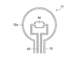

Classifications
-
- B—PERFORMING OPERATIONS; TRANSPORTING
- B32—LAYERED PRODUCTS
- B32B—LAYERED PRODUCTS, i.e. PRODUCTS BUILT-UP OF STRATA OF FLAT OR NON-FLAT, e.g. CELLULAR OR HONEYCOMB, FORM
- B32B7/00—Layered products characterised by the relation between layers; Layered products characterised by the relative orientation of features between layers, or by the relative values of a measurable parameter between layers, i.e. products comprising layers having different physical, chemical or physicochemical properties; Layered products characterised by the interconnection of layers
- B32B7/02—Physical, chemical or physicochemical properties
- B32B7/023—Optical properties
-
- G—PHYSICS
- G09—EDUCATION; CRYPTOGRAPHY; DISPLAY; ADVERTISING; SEALS
- G09F—DISPLAYING; ADVERTISING; SIGNS; LABELS OR NAME-PLATES; SEALS
- G09F9/00—Indicating arrangements for variable information in which the information is built-up on a support by selection or combination of individual elements
- G09F9/30—Indicating arrangements for variable information in which the information is built-up on a support by selection or combination of individual elements in which the desired character or characters are formed by combining individual elements
Definitions
- This disclosure relates to a decorative sheet, a display device with a decorative sheet, and an article with a decorative sheet.
- a display surface having black color is usually visually recognized in a state where no image is displayed.
- a fixed display device having a light transmitting portion having a desired shape is known.
- the light from the backlight arranged on the back surface of the light transmitting portion transmits through the light transmitting portion, so that the light transmitting portion is distinguished from the surrounding members and visually recognized.
- the light transmitting portion is visually recognized as a figure, a character, a pattern, or the like.
- the display surface having black color is visually recognized in a state where the region other than the light transmitting portion has black color and the backlight does not emit light.
- the region other than the light transmitting portion of the fixed display device has a color other than black, the light transmitting portion is distinguished from the surroundings and visually recognized as a figure, characters, or the like even if the backlight does not emit light.
- the image display device or fixed display device is required not only to have a function of displaying images, figures, characters, patterns, etc., but also to harmonize the design with the surrounding environment.
- a decorative sheet having a design in harmony with the surrounding environment on the observer side of the display surface of the display device, it is possible to impart a design in harmony with the surrounding environment to these display devices.
- a light transmitting portion composed of a large number of fine holes or the like is provided. As a result, images, figures, characters, patterns, etc. displayed on the display device are visually recognized via the decorative sheet.
- JPS64-9777A discloses a decorative display panel having a perspective portion.
- the release layer portion of the fine pattern of the negative image is lifted off from the substrate, so that a positive laminated fine pattern composed of the first colored layer, the concealing layer, and the second colored layer is formed on the substrate and lifted off.
- a fluoroscopic part is formed in the portion.
- JPH2-112895A discloses a light-shielding material for windows provided with a fine halftone dot-like light-shielding portion having a desired shape.
- a light-shielding portion is formed by laminating a first colored layer, a base concealing layer, and a second colored layer on a transparent substrate in this order.
- JPH2-112895A discloses an instrument dial that illuminates from the back surface of the character substrate.
- the instrument dial has a first print layer and a halftone dot print layer.
- the first print layer has a small light transmittance.
- the first print layer is formed on a light-transmitting plate in a region through which a large amount of light is transmitted.
- the halftone dot printing layer is also formed on the upper surface of the first printing layer.
- a decorative sheet can be manufactured by forming a design layer on a translucent base material and then providing a large number of fine holes in the design layer.
- the design layer has a predetermined design.
- the design layer can be formed by printing or the like.
- the holes are provided by laser machining.
- the decorative sheet has a light transmitting portion composed of holes. In this manufacturing method, all holes are formed by laser machining. Therefore, it takes time to manufacture the decorative sheet. Further, in this manufacturing method, the processing cost of the decorative sheet is high.
- An object of the present disclosure is to provide a decorative sheet, a display device with a decorative sheet, and an article with a decorative sheet that can be manufactured in a short time and at low cost.
- the decorative sheet of the present disclosure is A base material having light transmission and a design layer laminated on the base material are provided.
- the design layer has at least one elemental design layer.
- Each element design layer contains a plurality of halftone dots having the same color.
- the number X of the element design layers included in the design layer and the maximum halftone dot ratio Y (%) in each element design layer satisfy the following relationship. Y ⁇ 99.499 ⁇ X (-0.229)
- the number X of the element design layers and the maximum halftone dot ratio Y (%) may satisfy the following relationship. 51.2 x X (-0.382) ⁇ Y
- the coverage of the design layer by the halftone dots may be 50% or more and 99.5% or less.
- Each element design layer may have a thickness of 2 ⁇ m or more and 15 ⁇ m or less.
- the value of L * in the L * a * b * color system of the light incident from the front surface of the decorative sheet and reflected by the black plate is L.
- * 1, a * of the values a * 1, b * values and b * 1, in the decorative incident from the front surface of the sheet light L * a * b * color system, which is reflected by the decorative layer L * of the value of L * 2, a * value when the a * 2, b * value and b * 2
- the color difference Delta] E * ab is defined by the following formula was measured in SCI mode Delta] E * ab may be both 0.7 or more measured at Delta] E * ab and SCE type.
- ⁇ E * ab ((L * 1- L * 2 ) 2 + (a * 1- a * 2 ) 2 + (b * 1- b * 2 ) 2 ) 1/2
- the transmittance of visible light transmitted through the decorative sheet along the normal direction of the base material may be 0.5% or more and 55% or less.
- the values of a * and a * 3, b * of the value and b * 3 in the light of the L * a * b * color system exiting the D65 light source, in the normal direction of the substrate and emitted from the D65 light source the value of a * when a * 4, b * of the value and b * 4 in the light of the L * a * b * color system that has passed through the decorative sheet along, a * 3, b * 3 , A * 4 and b * 4 may satisfy the following relationship. ((A * 3- a * 4 ) 2 + (b * 3- b * 4 ) 2 ) 1/2 ⁇ 7
- the sheet resistance may be 1 ⁇ 10 6 ⁇ / ⁇ or more.
- the display device with a decorative sheet of the present disclosure is A display device with a display surface and It has the above-mentioned decorative sheet provided facing the display surface.
- the display device may be a dot matrix type display.
- the article with the decorative sheet of this disclosure With the above-mentioned decorative sheet, It has a resin portion arranged on the opposite side of the base material with respect to the design layer.
- a light source arranged between the decorative sheet and the resin portion may be further provided.
- the light source may be an LED.
- the article with the decorative sheet of this disclosure With the above-mentioned decorative sheet, It has a conductive pattern laminated on the decorative sheet.
- the invention's effect According to the present disclosure, it is possible to provide a decorative sheet, a display device with a decorative sheet, and an article with a decorative sheet that can be manufactured in a short time and at low cost.
- FIG. 1 is a diagram illustrating a first embodiment of the present disclosure, and is a perspective view schematically showing a display device with a decorative sheet in which a decorative sheet is incorporated.
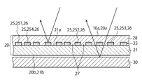
- FIG. 2 is a partial cross-sectional view showing a cross section of the decorative sheet.
- FIG. 3 is a partial plan view showing the first element design layer of the design layer of the decorative sheet.
- FIG. 4 is a partial plan view showing the second element design layer of the design layer.
- FIG. 5 is a partial plan view showing the third element design layer of the design layer.
- FIG. 6 is a partial plan view showing the fourth element design layer of the design layer.
- FIG. 7 is a partial plan view showing a design layer formed by superimposing each element design layer of FIGS. 3 to 6.
- FIG. 1 is a diagram illustrating a first embodiment of the present disclosure, and is a perspective view schematically showing a display device with a decorative sheet in which a decorative sheet is incorporated.
- FIG. 2 is a partial cross-sectional
- FIG. 8 is a diagram illustrating a method of calculating the halftone dot ratio.
- FIG. 9 is a diagram illustrating a method of calculating the halftone dot ratio.
- FIG. 10 is a diagram illustrating an example of a method for adjusting the maximum halftone dot ratio.
- FIG. 11 is a diagram illustrating another example of the method of adjusting the maximum halftone dot ratio.
- FIG. 12 is a partial cross-sectional view schematically showing the state of reflection of light incident from the front surface of the decorative sheet when the black plate is arranged on the back side of the decorative sheet.
- FIG. 13 is a partial cross-sectional view schematically showing how the light emitted from the D65 light source passes through the decorative sheet.
- FIG. 14 is a partial cross-sectional view showing a modified example of the decorative sheet.
- FIG. 15 is a partial cross-sectional view showing another modified example of the decorative sheet.
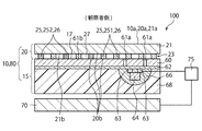
- FIG. 16 is a view for explaining the second embodiment of the present disclosure, and is a cross-sectional view showing an example of an electronic device with a decorative sheet in which a decorative sheet is incorporated.
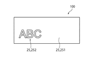
- FIG. 17 is a plan view showing the electronic device with the decorative sheet of FIG.
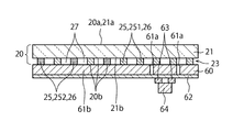
- FIG. 18 is a plan view showing the electronic device with the decorative sheet of FIG.
- FIG. 19 is a diagram illustrating an example of a method of manufacturing a display device with a decorative sheet for an electronic device with a decorative sheet.
- FIG. 20 is a plan view showing a decorative sheet of the display device with a decorative sheet of FIG. FIG.
- FIG. 21 is a diagram illustrating an example of a method of manufacturing a display device with a decorative sheet.
- FIG. 22 is a plan view showing a pattern layer of the display device with a decorative sheet.
- FIG. 23 is a diagram illustrating an example of a method of manufacturing a display device with a decorative sheet.
- FIG. 24 is a diagram illustrating an example of a method of manufacturing a display device with a decorative sheet.
- FIG. 25 is a diagram illustrating an example of a method of manufacturing a display device with a decorative sheet.
- FIG. 26 is a diagram illustrating an example of a method of manufacturing a display device with a decorative sheet.
- FIG. 27 is a diagram illustrating an example of a method of manufacturing a display device with a decorative sheet.
- FIG. 28 is a cross-sectional view showing a modified example of the display device with a decorative sheet.
- FIG. 29 is a cross-sectional view showing another modification of the display device with a decorative sheet.
- FIG. 30 is a cross-sectional view showing still another modification of the display device with a decorative sheet.
- FIG. 31 is a plan view showing the display device with a decorative sheet of FIG.
- FIG. 32 is a plan view showing an example of a conductive pattern in an article with a decorative sheet.
- FIG. 33 is a plan view showing another example of the conductive pattern.
- FIG. 34 is a plan view showing still another example of the conductive pattern.
- the terms "board”, “sheet”, and “film” are not distinguished from each other based only on the difference in designation.
- the “sheet” also includes a member called a “plate” or a “film”.
- the "plate surface (sheet surface, film surface)” is a target plate-shaped member (sheet) when the target plate-shaped (sheet-shaped, film-shaped) member is viewed as a whole and in a broad view. Refers to a surface that coincides with the direction in which the shaped member (shaped member, film-shaped member) extends. Further, the normal direction used for the plate-shaped (sheet-shaped, film-shaped) member refers to the direction in which the normal line extends with respect to the plate surface (sheet surface, film surface) of the member.
- planar view refers to a state in which symmetrical plate-shaped (sheet-shaped, film-shaped) members are viewed from the normal direction of the members.
- having a rectangular shape in a plan view means that a plate-shaped member has a rectangular shape when the member is viewed from the normal direction with respect to the plate surface. do.
- a decorative sheet arranged and used on the observer side of the display surface of a video display device such as a liquid crystal display device and an organic EL display device
- the decorative sheet of the present disclosure may be used as a decorative sheet arranged and used on the observer side of the display surface of the fixed display device, or the like. It may be used for various purposes.
- the fixed display device has a light transmitting portion arranged on the observer side of the backlight.
- the light transmitting portion has a desired shape. In the fixed display device, the light from the backlight is transmitted through the light transmitting portion. As a result, the light transmitting portion is distinguished from the surroundings and visually recognized as a pattern such as a figure or a character.
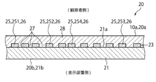
- FIG. 1 is a perspective view schematically showing a display device 10 with a decorative sheet in which the decorative sheet 20 is incorporated.
- FIG. 2 is a partial cross-sectional view showing a cross section of the decorative sheet 20.
- the display device 10 with a decorative sheet of the present embodiment includes a display device 15 and a decorative sheet 20.
- the decorative sheet 20 is arranged so as to face the display surface 17 of the display device 15.
- the display device 15 of the present embodiment is, for example, a dot matrix type display.
- the dot matrix type display is, for example, a liquid crystal display (LCD), an organic EL display (OLED), a micro LED display, a quantum dot (QD) display, or the like.
- the display surface 17 includes a display area 17A and a non-display area 17B.
- the display area 17A is an area in which an image such as a moving image or a still image is displayed.
- the non-display area 17B is an area in which no image is displayed. In the example shown in FIG.
- the display area 17A has a rectangular contour in a plan view of the display surface 17.
- the non-display area 17B has a frame-like shape surrounding the display area 17A.
- the display device 10 with a decorative sheet has an demitsu surface 10a.
- Light-emitting surface 10a is a surface for emitting image light L i that may be visible to the observer 5 through the decorating sheet 20 is emitted from the display device 15.
- the decorative sheet 20 constitutes the light emitting surface 10a.
- a transparent protective layer or the like may be further provided on the observer 5 side of the decorative sheet 20, and the protective layer or the like may form the light emitting surface 10a of the display device 10 with the decorative sheet.
- the decorative sheet 20 is arranged on the observer 5 side of the display device 15.
- the decorative sheet 20 imparts design to the display device 15.
- the decorative sheet 20 imparts a design to the display device 15 in harmony with the surrounding environment.
- the decorative sheet 20 is arranged so as to cover the display area 17A and the non-display area 17B of the display surface 17.
- the decorative sheet 20 may be arranged so as to cover only the display area 17A of the display surface 17.
- a predetermined design to be observed from the observer 5 side is given to the decorative sheet 20.
- the decorative sheet 20 has a light transmitting portion 27 described later.
- Light transmitting unit 27 transmits the display device 15 side image light L i emitted from the display device 15 to the viewer 5 side.
- image light L i is emitted from the display device 15, and emitted from the image light L i is decorated through the light transmitting portion 27 of the seat 20 light-emitting surface 10a, the image light L i is observed It is visually recognized by the person 5. Therefore, the display device 10 with the decorative sheet has a different appearance depending on whether the image light Li is emitted from the display device 15 or not.
- the decorative sheet 20 includes a base material 21 and a design layer 23.
- the base material 21 has light transmittance.
- the design layer 23 is laminated on the base material 21.
- the decorative sheet 20 has a coating layer 28.
- the coating layer 28 covers the base material 21 and the design layer 23 from the observer 5 side.
- the decorative sheet 20 has a first surface 20a and a second surface 20b.
- the first surface 20a faces the observer side.
- the second surface 20b faces the side opposite to the first surface 20a (display device 15 side).
- the first surface 20a of the decorative sheet 20 is the light emitting surface 10a of the display device 10 with the decorative sheet.
- the base material 21 is a member that supports the design layer 23.
- the base material 21 has a first surface 21a and a second surface 21b.
- the first surface 21a faces the observer 5 side.
- the second surface 21b faces the side opposite to the first surface 21a (display device 15 side).
- the design layer 23 is provided on the first surface 21a of the base material 21.
- the substrate 21 is a transparent substrate.
- the base material 21 preferably has a transmittance of 80% or more in visible light. It is more preferable that the base material 21 has a transmittance of 84% or more in visible light.
- the transmittance of visible light is determined by mounting an integrating sphere unit “ISN-723" on a spectrophotometer “V-670” manufactured by JASCO Corporation and using this spectrophotometer to have a wavelength of 380 nm to 780 nm. It is the average value of the transmittance at each wavelength when the light transmittance in all directions is measured within the range.
- the base material 21 preferably has a light reflectance of 20% or less in the visible light region. It is more preferable that the base material 21 has a light reflectance of 16% or less in the visible light region.
- the light reflectance may be measured using a spectrocolorimeter "CM-700d” manufactured by Konica Minolta.
- the base material 21 may be a plate, sheet or film made of, for example, glass or resin.
- resin film various resin films used as a base material of an optical member may be preferably used.
- acrylic resin, ABS resin, polymethyl methacrylate, polyethylene terephthalate, polyethylene naphthalate, polycarbonate, polystyrene, and cyclic polyolefin may be used as the material of the base material 21.
- the base material 21 may have one layer of resin film.
- the base material 21 may have two or more layers of resin film.
- the thickness of the base material 21 may be 50 ⁇ m or more and 500 ⁇ m or less.
- the second surface 21b of the base material 21 is the second surface 20b of the decorative sheet 20.
- the coating layer 28 covers and protects the base material 21 and the design layer 23 from the observer 5 side.
- the surface of the covering layer 28 facing the observer 5 side is the first surface 20a of the decorative sheet 20.
- the coating layer 28 is a transparent member.
- the coating layer 28 preferably has a transmittance of 80% or more in visible light.
- the coating layer 28 more preferably has a transmittance of 84% or more in visible light.
- the coating layer 28 may be formed by sticking a glass or resin film on the base material 21 (first surface 21a) and the design layer 23. Further, the coating layer 28 may be formed by applying a fluid resin material and curing it.
- the resin material for forming the coating layer 28 various resin materials used as optical members may be preferably used.
- the same resin material as the resin material constituting the base material 21 may be used.
- Design layer 23 displays a design image light L i from the display device 15 is viewed from the observer 5 when not emitted.
- This design is, for example, a picture, a photograph, a figure, a pattern, a mark, a character, a color, or the like.
- the design may be a design that can be harmonized with the environment around the place where the display device 15 is installed. As such a design, a pattern having an appearance similar to that of wood or marble may be used. Further, the design layer 23 may have a pattern of a single color.
- the design layer 23 has at least one element design layer 25.
- One element design layer 25 displays a monochromatic element design.
- each element design layer 25 includes a plurality of halftone dots 26 having the same color.
- the element design is represented by a set of halftone dots 26.
- each element design layer 25 displays element designs having different colors from each other.
- the design to be displayed by the design layer 23 is formed by superimposing the plurality of element design layers 25.
- each elemental design is a design in which the design to be displayed by the design layer 23 is decomposed for each color.
- the design layer 23 of the present embodiment includes four elemental design layers 25 (251 to 254).
- the first element design layer 251 displays an element design having black color (BK).
- the second element design layer 252 displays an element design having a blue color (C).
- the third element design layer 253 displays an element design having a red color (M).
- the fourth element design layer 254 displays an element design having a yellow color (Y). That is, the first element design layer 251 is composed of a set of halftone dots 26 having black color.
- the second element design layer 252 is composed of a set of halftone dots 26 having blue color.
- the third element design layer 253 is composed of a set of halftone dots 26 having a red color.
- the fourth element design layer 254 is composed of a set of halftone dots 26 having yellow color.
- the specific configuration of the element design layer 25 is arbitrarily determined. The specific configuration is, for example, the number of element design layers 25, the colors displayed by each element design layer 25, and the order in which the plurality of element design layers 25 are superposed.
- FIG. 3 is a partial plan view showing the first element design layer 251 (25).
- FIG. 4 is a partial plan view showing the second element design layer 252 (25).
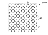
- FIG. 5 is a partial plan view showing the third element design layer 253 (25).
- FIG. 6 is a partial plan view showing the fourth element design layer 254 (25).
- the halftone dots 26 are composed of fine dot-shaped colored regions.
- the halftone dots 26 have a contour having a circular shape in a plan view.
- the diameter of the halftone dots 26 may be, for example, 72 ⁇ m or more and 365 ⁇ m or less.
- the diameter of the halftone dots 26 may be 72 ⁇ m or more and 270 ⁇ m or less. ..
- each halftone dot 26 may have the same area (diameter) or different area (diameter) from each other.
- Such halftone dots 26 can be formed on the base material 21 by using a printing technique such as screen printing.
- the halftone dots 26 are arranged using, for example, an AM screen.
- the plurality of halftone dots 26 are regularly arranged along a predetermined arrangement direction.
- the plurality of halftone dots 26 are arranged on each intersection of a predetermined virtual grid.
- the shade in the element design displayed by the element design layer 25 is represented by the size of the area (diameter) of the halftone dots 26.
- each halftone dot 26 is regularly arranged using an AM screen.
- the resolution of the halftone dots 26 in the element design layer 25 may be, for example, 70 dpi or more and 150 dpi or less.
- each halftone dot 26 has the same area (diameter) as each other for easy understanding.
- the plurality of element design layers 25 may be laminated by differently arranging the halftone dots 26 among the plurality of element design layers 25.
- the arrangement direction D 1 of the dot 26 of the first element design layer 251 as a reference.
- the arrangement directions D 2 to D 4 of the net points 26 of the second element design layer 252 to the fourth element design layer 254 and the arrangement direction D 1 have a predetermined angle ⁇ .
- the first element design layer 251 to the fourth element design layer 254 are laminated so as to have.
- the arrangement direction D 2 of the halftone dots 26 of the second element design layer 252 has an angle ⁇ of 15 degrees counterclockwise with respect to the arrangement direction D 1.
- the arrangement direction D 3 of the halftone dots 26 of the third element design layer 253 has an angle ⁇ of 45 degrees counterclockwise with respect to the arrangement direction D 1.
- the arrangement direction D 4 of the halftone dots 26 of the fourth element design layer 254 has an angle ⁇ of 75 degrees counterclockwise with respect to the arrangement direction D 1.
- FIG. 7 shows a partial plan view of the design layer 23 formed by superimposing the first element design layer 251 to the fourth element design layer 254.
- FIG. 7 is a view showing the first element design layer 251 to the fourth element design layer 254 stacked in this order on the base material 21 as viewed from the fourth element design layer 254 side (observer 5 side). ..
- the element design layers 251 to 254 are arranged so that the arrangement directions D 1 to D 4 of the halftone dots 26 have a predetermined angle with each other. Therefore, even if a slight misalignment occurs between the element design layers 251 to 254, it is possible to suppress the occurrence of moire due to this misalignment.
- the number X of the element design layers 25 included in the design layer 23 and the maximum halftone dot ratio Y (%) in each element design layer 25 (251 to 254) have the following relationship. Meet. Y ⁇ 99.499 ⁇ X (-0.229) ... (Equation 1)
- X is a natural number. For example, when the number X of the element design layers 25 included in the design layer 23 is 4, the maximum halftone dot ratio Y in each element design layer 25 is about 72.4% or less.
- the halftone dot ratio of a certain layer is occupied by the portion of the halftone dots 26 located in the predetermined area of the layer in the plan view of the layer.
- the ratio of the area is expressed as a percentage.
- the maximum halftone dot ratio Y is the largest halftone dot ratio among the halftone dot ratios in each region of the layer. Therefore, for example, when the maximum halftone dot ratio Y in the element design layer 25 is 60%, the halftone dot ratio is 60% or less in all the regions in the element design layer 25. In other words, when the maximum halftone dot ratio Y in the element design layer 25 is 60%, there is no region in the element design layer 25 in which the halftone dot ratio exceeds 60%.
- the maximum halftone dot ratio Y in each element design layer 25 satisfies the above equation 1 means that the maximum halftone dot ratio Y in all the element design layers 25 satisfies the above equation 1, respectively.
- the design layer 23 includes the first element design layer 251 to the fourth element design layer 254 will be described below.
- the number X of the element design layer 25 included in the design layer 23 is 4.
- the maximum halftone dot ratio Y in the above equation 1 satisfies the above equation 1.
- the largest halftone dot ratio Y is defined as Y max. That is, of the maximum halftone dot ratios Y in all the element design layers 25, the largest maximum halftone dot ratio Y is defined as Y max.
- Y max satisfies the following equation 1-2
- the maximum halftone dot ratio Y in each element design layer 25 satisfies the above equation 1.
- the largest maximum halftone dot ratio Y max among the maximum halftone dot ratio Y in each element design layer 25 is the above equation 1-. It is the same as satisfying 2.
- the number X of the element design layers 25 included in the design layer 23 and the maximum halftone dot ratio Y (%) in each element design layer 25 (251 to 254) satisfy the following relationship.
- Equation 1-3 For example, when the number X of the element design layers 25 included in the design layer 23 is 4, the maximum halftone dot ratio Y in each element design layer 25 is about 68.3% or less.
- the largest maximum halftone dot ratio Y max satisfies the following relationship. Y max ⁇ 95.7 x X (-0.243) ... (Equation 1-4)
- the coverage ratio by the halftone dots 26 in the entire design layer 23 is large.
- the coverage ratio by the halftone dots 26 in the entire design layer 23 after the plurality of element design layers 25 are superposed may be 99.5% or less. Accordingly, the image light L i emitted from the display device 15 is well visible from the observer 5.
- the maximum halftone dot ratio Y in one element design layer 25 is small.
- the coverage ratio by the halftone dots 26 in the design layer 23 after the plurality of element design layers 25 are superposed does not greatly exceed 99.5%. Therefore, a sufficient area of the light transmitting portion 27 in the design layer 23 can be secured.
- the coverage ratio by the halftone dots 26 in the entire design layer 23 after the plurality of element design layers 25 are superposed may be 95% or less. Accordingly, the image light L i emitted from the display device 15 is better viewed from the observer 5.
- the coverage by the halftone dots 26 in the design layer 23 after the plurality of element design layers 25 are superposed does not greatly exceed 95%. Therefore, the area of the light transmitting portion 27 in the design layer 23 can be further sufficiently secured.
- the transmittance of visible light at the halftone dots 26 may be 0% or more and 30% or less. Preferably, the transmittance of visible light at the halftone dots 26 may be 10% or more and 25% or less.
- the transmittance of visible light at the halftone dots 26 is the transmittance at the one-layer halftone dots 26. As described above, the transmittance of visible light at the halftone dots 26 is relatively small. In this case, the maximum halftone dot ratio Y in each element design layer 25 satisfies the above equation 1, or the largest maximum halftone dot ratio Y max of the maximum halftone dot ratio Y satisfies the above equation 1-2. A sufficient area of the transmission portion 27 can be secured. Accordingly, emitted from the display device 15 can be sufficiently ensured amount of the image light L i which passes to the viewer 5 side through the light transmitting portion 27.
- Table 1 shows the decorative sheet 20 when the number X of the element design layers 25 included in the design layer 23 and the maximum halftone dot ratio Y in each element design layer 25 are changed for a plurality of samples of the decorative sheet 20. The evaluation of is shown.
- the "sample number” is a serial number assigned to each sample.
- the “number X of element design layers” is the number X of the element design layers 25 included in the design layer 23 of each sample.
- the “maximum halftone dot ratio Y (%)” is the maximum halftone dot ratio Y (%) in each element design layer 25.
- the “coverage (%)” is the coverage (%) of the halftone dots 26 in the design layer 23.
- the “transmittance (%)” is the transmittance (%) of visible light transmitted through each sample.
- “Evaluation” is an evaluation for each sample.
- the transmittance of visible light and the color reflectance of the decorative sheet 20 of the display device 10 with a decorative sheet (simply referred to as “display device” in Table 1) in which the decorative sheet 20 of each sample is incorporated are visually determined. evaluated.
- Each element design layer 25 constituting the design layer 23 has a different color from each other.
- the color of the element design layer 25 of the first layer is yellow.
- the color of the element design layer 25 of the second layer is blue.
- the color of the element design layer 25 of the third layer is red.
- the color of the element design layer 25 of the fourth layer is brown.
- the color of the element design layer 25 of the fifth layer is flesh color.
- the color of the element design layer 25 of the sixth layer is black. Therefore, for example, in the samples 9 to 12 in which "the number X of the element design layers X" is 3, the design layer 23 is the element design layer 25 having a yellow color, the element design layer 25 having a blue color, and the element design having a red color. It has a layer 25 and.
- the thickness of each element design layer 25 is 15 ⁇ m.
- the design layer 23 has two elemental designs in which the colors and arrangements of the halftone dots 26 are different from each other and the maximum halftone dot ratio Y is 83.5%.
- the coverage of the halftone dots 26 in the design layer 23 is about 99.4%. In this case, can be secured transmittance required to visually recognize the observer 5 image light L i from the display device 15.
- the coverage of the halftone dots 26 in the design layer 23 is about 99.4%. ..
- the coverage of the halftone dots 26 in the design layer 23 is about 99.4%.
- the above equation 1 is an approximate equation based on these data.
- the coverage of the halftone dots 26 in the design layer 23 is 95%.
- the coverage of the halftone dots 26 in the design layer 23 is about 95%.
- the maximum halftone dot ratio Y in the element design layer 25 is measured as follows.
- the element design layer 25 is photographed using a digital microscope "VH-5500" manufactured by KEYENCE CORPORATION.
- VH-5500 manufactured by KEYENCE CORPORATION.
- the coverage of halftone dots 26 in a square region having a side length of 1 mm is calculated.
- the coverage of the halftone dots 26 calculated at the location where the coverage by the halftone dots 26 is the largest is the maximum halftone dot ratio Y in the element design layer 25.
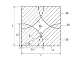
- FIGS. 8 and 9 are diagrams illustrating a method of calculating the halftone dot ratio.
- FIG. 8 is a diagram illustrating a method of calculating the halftone dot ratio when the arrangement pitch a of the halftone dots 26 is equal to or larger than the diameter b of the halftone dots 26, and
- FIG. 9 is a diagram in which the arrangement pitch a of the halftone dots 26 is the halftone dots. It is a figure explaining the calculation method of the halftone dot ratio when it is smaller than the diameter b of 26.
- a unit section 50 having the centers of the four halftone dots 26 as vertices. As shown in FIGS. 8 and 9, the unit compartment 50 has a square contour. The length of one side of the unit section 50 is a. Therefore, the area of the unit section 50 is a 2.
- A is one side of the unit compartment 50.
- P is a point where the contours of two halftone dots 26 centered on both ends of the side A intersect each other.
- ⁇ (rad) is the angle between the straight line B connecting one end O of the side A and the point P and the side A.
- Area of the region covered by the dot 26 has a diameter b in a unit compartment 50, ⁇ ⁇ (b / 2) of two adjacent two dot 26 How to have overlapped portion 4 times the area S 1 of Obtained by subtracting the area.
- the area S 1 is obtained as follows.
- the arrangement pitch a of the halftone dots 26 and the diameter b of the halftone dots 26 can be measured using a digital microscope "VH-5500" manufactured by KEYENCE CORPORATION.
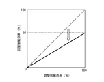
- FIG. 10 is a diagram illustrating an example of an adjustment method of the maximum halftone dot ratio Y.
- FIG. 11 is a diagram illustrating another example of the method for adjusting the maximum halftone dot ratio Y.
- the number X of the element design layers 25 included in the design layer 23 is 4, and the maximum halftone dot ratio Y of each element design layer 25 is 60%.
- the halftone dot ratio of each portion of the halftone dot image before adjustment of the maximum halftone dot ratio Y is on the horizontal axis.
- the vertical axis is the halftone dot ratio of each part of the halftone dot image after adjusting the maximum halftone dot ratio Y. Further, in FIGS.
- the halftone dot ratio of the halftone dot image before the adjustment of the maximum halftone dot ratio Y is shown by a broken line
- the halftone dot ratio of the halftone dot image after the adjustment of the maximum halftone dot ratio Y is shown by a solid line. ..
- the following may be performed.
- a predetermined color image to be a design displayed by the design layer 23 is decomposed into four-color images.
- the four-color images are superposed to form the color image.
- the four-color image includes a black (BK) image, a blue (C) image, a red (M) image, and a yellow (Y) image.
- the image of each color is converted into a halftone dot image so that the halftone dot ratio in the image is 0% to 100%.
- the halftone dot ratio of the portion where the halftone dot ratio exceeds 60% is adjusted to 60%. As a result, it is possible to create a halftone dot image forming the element design of each element design layer 25.
- a halftone dot image forming the element design of each element design layer 25 may be created as follows. First, a predetermined color image to be a design displayed by the design layer 23 is decomposed into four-color images. The four-color images are superposed to form the color image. The four-color image includes a black (BK) image, a blue (C) image, a red (M) image, and a yellow (Y) image. Next, the image of each color is converted into a halftone dot image so that the halftone dot ratio in the image is 0% to 100%. After that, as shown in FIG.
- the halftone dot ratio of the entire halftone dot image is reduced so that the halftone dot ratio of the portion where the halftone dot ratio was 100% before the adjustment becomes 60%.
- the halftone dot image of each color is converted into a halftone dot image such that the halftone dot ratio of the entire halftone dot image is 0% or more and 60% or less.
- the design layer 23 has a plurality of element design layers 25 superposed on each other, the design layer 23 has a region (light transmitting portion 27) in which halftone dots 26 do not exist along the normal direction.
- the light incident from the second surface 20b of the decorative sheet 20 passes through the light transmitting portion 27 in the design layer 23 and is emitted from the first surface 20a.
- the number X of the element design layers 25 included in the design layer 23 and the maximum halftone dot ratio Y (%) in each element design layer 25 (251 to 254) are expressed in the above equation 1. Meet. As a result, a sufficient area of the light transmitting portion 27 in the design layer 23 can be secured.
- emitted from the display device 15 can be sufficiently ensured amount of the image light L i emitted toward the observer 5 side through the light transmitting portion 27 of the design layer 23. That is, when the image light L i is emitted from the display device 15, the image light L i is well visible from the observer 5.
- the halftone dots 26 are formed on the base material 21 by using a printing technique such as screen printing. Therefore, in order to provide the light transmitting portion 27 on the design layer 23, it is not necessary to use laser machining, which requires a large machining time and machining cost. Further, by configuring the design displayed by the design layer 23 with halftone dots 26, it is not necessary to align (align) between the element design layers 25 with high accuracy. As a result, the decorative sheet 20 can be manufactured in a short time and at low cost.
- the degree of freedom in arranging each color represented by the halftone dots 26 is increased. Further, by forming the design displayed by the design layer 23 with halftone dots 26, the reproducibility of colors and shades is improved. In addition, the light transmitting portion 27 will have a random shape and arrangement. Therefore, when a video display device having a large number of regularly arranged pixels is used as the display device 15 and the display device 15 and the decorative sheet 20 are overlapped with each other, it is possible to effectively suppress the occurrence of moire. ..
- Such an image display device is, for example, a liquid crystal display device or an organic EL display device.
- the number X of the element design layers 25 included in the design layer 23 and the maximum halftone dot ratio Y (%) in each element design layer 25 (251 to 254) are in addition to the relationship of the above formula 1. Further, the following relationship may be satisfied. 51.2 ⁇ X ( ⁇ 0.382) ⁇ Y ⁇ ⁇ ⁇ (Equation 4) X is a natural number. For example, when the number X of the element design layers 25 included in the design layer 23 is 4, the maximum halftone dot ratio Y in each element design layer 25 is about 30.1% or more. When the maximum halftone dot ratio Y satisfies Equation 4, the area of the light transmitting portion 27 can be sufficiently secured, and the light reflectance in the design layer 23 can be sufficiently secured. Thus, when image light L i from the display device 15 is not emitted, the design with the design layer 23 of the decorative sheet 20 is satisfactorily visible from the observer 5.
- the coverage of the halftone dots 26 in the design layer 23 is about 50%.
- the above equation 4 is an approximate equation based on these data.
- the coverage ratio by the halftone dots 26 in the design layer 23 having a plurality of elemental design layers 25 superposed on each other may be 50% or more and 99.5% or less.
- the area of the light transmitting portion 27 in the design layer 23 can be further sufficiently secured. Accordingly, emitted from the display device 15, a light amount of the image light L i can be more sufficiently secured emitted toward the observer 5 side through the light transmitting portion 27 of the design layer 23. That is, when the image light L i is emitted from the display device 15, the image light L i is better visible from the observer 5.
- the design layer 23 includes four element design layers 25 that are superposed on each other.
- the number X of the element design layer 25 included in the design layer 23 is not limited to this.
- the design layer 23 may include one element design layer 25. Further, the design layer 23 may include two, three or five or more element design layers 25 which are overlapped with each other.
- the number X of the element design layers 25 forming the design layer 23 may be 6 or less. Further, the number X of the element design layers 25 forming the design layer 23 may be 5 or less. In this case, a sufficient area of the light transmitting portion 27 in the design layer 23 can be secured.
- Each element design layer 25 may have a thickness of 2 ⁇ m or more and 15 ⁇ m or less.
- the thickness of the element design layer 25 is 2 ⁇ m or more, sufficient light reflectance can be secured at the halftone dots 26 included in the element design layer 25. Therefore, when image light L i from the display device 15 is not emitted, the design with the design layer 23 of the decorative sheet 20 is satisfactorily visible from the observer 5.
- the thickness of the element design layer 25 is 2 ⁇ m or more, when a plurality of halftone dots 26 overlap in the normal direction of the design layer 23, the halftone dots 26 are closer to the display device 15 than the halftone dots 26. It can absorb the light emitted from the other halftone dots 26 located at.
- each element design layer 25 may have a thickness of 5 ⁇ m or more and 15 ⁇ m or less.
- Each element design layer 25 may have a thickness of 9 ⁇ m or more and 15 ⁇ m or less.
- FIG. 12 schematically shows a state of reflection of light incident from the front surface (first surface) 20a of the decorative sheet 20 when the black plate 30 is arranged on the back surface (second surface) 20b side of the decorative sheet 20.
- L * 1 a * 1 and b * 1 were incident from the front surface 20a of the decorative sheet 20 and reflected by the black plate 30 when the black plate 30 was arranged on the back surface 20b side of the decorative sheet 20, respectively.
- L * 2 a * 2 and b * 2 are each decorative sheet 20 is incident from the front surface 20a of the light reflected by the decorative layer 23 L * a * b * L * value in the color system, a The value of * and the value of b * .
- the color difference ⁇ E * ab defined by the following equation may be 0.7 or more in the SCI method and 0.7 or more in the SCE method.
- ⁇ E * ab ((L * 1- L * 2 ) 2 + (a * 1- a * 2 ) 2 + (b * 1- b * 2 ) 2 ) 1/2 ... (Equation 5)
- the black plate 30 is a black plate having a light transmittance of 0%.
- the black plate 30 may be, for example, a black acrylic plate.
- the black plate 30 may be attached to the second surface 20b of the decorative sheet 20 using an optical adhesive.
- the optical adhesive for example, a transparent adhesive sheet known as OCA (Optical Clear Adhesive) may be used.
- L * 1 and L * 2 are obtained as follows. First, the transmittance of visible light in the entire design layer 23 is measured using a spectrocolorimeter "CM-700d” manufactured by Konica Minolta. Next, a square region having a side length of 1 mm is set at a portion of the design layer 23 having the lowest visible light transmittance. After that, using the spectrophotometer "CM-700d” described above, the illumination diameter (diameter) is set to 11 mm, the measurement diameter (diameter) is set to 8 mm, and L * 1 , a * is set in the light transmitting portion 27 in the square region. 1, and b * 1 is measured. Further, the values of L * 2 , a * 2 , and b * 2 are measured in the area where the halftone dots 26 exist in the square area.
- the SCI (Special Component Inc.) method is a method for measuring color including specularly reflected light.
- the SCE (Special Component Exclude) method is a method of measuring color excluding specularly reflected light. In the above-mentioned spectrophotometer CM-700d, the SCI method and the SCE method can be switched depending on the setting.
- both ⁇ E * ab measured by the SCI method and ⁇ E * ab measured by the SCE method may be 1.0 or more.
- Measured Delta] E * ab in the measured Delta] E * ab and SCE type in SCI scheme it may be both 1.5 or more.
- the transmittance of visible light transmitted through the decorative sheet 20 in the normal direction of the base material 21 may be 0.5% or more and 55% or less.
- the transmittance of the visible light is 0.5% or more, emitted from the display device 15 can be sufficiently ensured amount of the image light L i emitted toward the observer 5 side through the decorating sheet 20 .. That is, when the image light L i is emitted from the display device 15, the image light L i is well visible from the observer 5. Further, when the transmittance of the visible light is 55% or less, the density of the design displayed by the design layer 23 can be sufficiently secured.
- the transmittance of visible light transmitted through the decorative sheet 20 in the normal direction of the base material 21 may be 5% or more and 55% or less.
- the transmittance of visible light transmitted through the decorative sheet 20 in the normal direction of the base material 21 may be 10% or more and 35% or less. More preferably, the transmittance of visible light transmitted through the decorative sheet 20 in the normal direction of the base material 21 may be 15% or more and 25% or less.
- FIG. 13 schematically shows how the light emitted from the D65 light source 40 passes through the decorative sheet 20.
- a * 3 and b * 3 are the values of a * and b * in the L * a * b * color system of the light emitted from the D65 light source 40, respectively.
- a * 4 and b * 4 are the values of a * in the L * a * b * color system of the light emitted from the D65 light source 40 and transmitted through the decorative sheet 20 along the normal direction of the base material 21, respectively.
- b * values. a * 3 , b * 3 , a * 4 and b * 4 may satisfy the following relationships.
- the D65 light source 40 is a CIE standard light source D65.
- the integrating sphere unit "ISN-723" is attached to the spectrophotometer "V-670" manufactured by JASCO Corporation, and light is transmitted in all directions. Obtained by measuring the rate.
- the sheet resistance of the decorative sheet 20 may be 1 ⁇ 10 6 ⁇ / ⁇ or more. If the sheet resistance of the decorative sheet 20 is small, the touch panel may not be able to appropriately detect the approach of a conductor such as an operator's finger via the decorative sheet 20. On the other hand, when the sheet resistance of the decorative sheet 20 is 1 ⁇ 10 6 ⁇ / ⁇ or more, the approach of the conductor can be appropriately detected by the touch panel via the decorative sheet 20. When the display device 15 is a display of the dot matrix type, the sheet resistance of the decorative sheet 20 may be 1 ⁇ 10 8 ⁇ / ⁇ or more. The sheet resistance of the decorative sheet 20 can be measured using, for example, a resistivity meter (High Lester UP MCP-HT450) manufactured by Mitsubishi Chemical Analytech Co., Ltd.
- a resistivity meter High Lester UP MCP-HT450
- the decorative sheet 20 described above can be manufactured as follows. First, the first element design layer 251 and the second element design layer 252, the third element design layer 253, and the fourth element design layer 254 are printed in this order on the first surface 21a of the base material 21 by screen printing. ..
- Each of the element design layers 251 to 254 includes halftone dots 26. At this time, the arrangement direction D 1 of the halftone dots 26 in the first element design layer 251 , the arrangement direction D 2 of the halftone dots 26 in the second element design layer 252 , and the arrangement direction D 3 of the halftone dots 26 in the third element design layer 253.
- each element design layer 251-254 is disposed.
- the coating layer 28 is formed on the base material 21 and the design layer 23.
- the coating layer 28 may be formed of glass, a resin film, or a cured resin material.
- the coating layer 28 may be formed by sticking a glass or resin film on the base material 21 and the design layer 23. Further, the coating layer 28 may be formed by applying a fluid resin material on the base material 21 and the design layer 23 and curing the coating layer 28.
- the decorative sheet 20 of the present embodiment includes a light-transmitting base material 21 and a design layer 23 laminated on the base material 21, and the design layer 23 has at least one element design layer 25.
- Each element design layer 25 includes a plurality of net points 26 having the same color, the number X of the element design layers 25 included in the design layer 23, and the maximum net point ratio Y (%) in each element design layer 25. Satisfies the following relationship. Y ⁇ 99.499 ⁇ X (-0.229) ... (Equation 1)
- the display device 10 with a decorative sheet of the present embodiment has a display device 15 having a display surface 17 and the above-mentioned decorative sheet 20 provided facing the display surface 17.
- the area of the light transmitting portion 27 can be sufficiently secured in the design layer 23 having the plurality of element design layers 25 superposed on each other. Accordingly, emitted from the display device 15 can be sufficiently ensured amount of the image light L i emitted toward the observer 5 side through the light transmitting portion 27 of the design layer 23. That is, when the image light L i is emitted from the display device 15, the image light L i is well visible from the observer 5.
- the decorative sheet 20 and the display device 10 with the decorative sheet it is not necessary to use laser processing which requires a large processing time and processing cost in order to provide the light transmitting portion 27 on the design layer 23. Further, by configuring the design displayed by the design layer 23 with halftone dots 26, it is not necessary to align (align) between the element design layers 25 with high accuracy. As a result, the decorative sheet 20 can be manufactured in a short time and at low cost.
- the degree of freedom in arranging each color represented by the halftone dots 26 is increased. Further, by forming the design displayed by the design layer 23 with halftone dots 26, the reproducibility of colors and shades is improved. In addition, the light transmitting portion 27 will have a random shape and arrangement. Therefore, when a video display device having a large number of regularly arranged pixels is used as the display device 15 and the display device 15 and the decorative sheet 20 are overlapped with each other, it is possible to effectively suppress the occurrence of moire. ..
- Such an image display device is, for example, a liquid crystal display device or an organic EL display device.
- the number X of the element design layer 25 and the maximum halftone dot ratio Y (%) satisfy the following relationship. 51.2 ⁇ X ( ⁇ 0.382) ⁇ Y ⁇ ⁇ ⁇ (Equation 4)
- the coverage of the design layer 23 by the halftone dots 26 is 50% or more and 99.5% or less.
- the area of the light transmitting portion 27 in the design layer 23 can be further sufficiently secured. Accordingly, emitted from the display device 15, the amount of image light L i can be more sufficiently secured emitted toward the observer 5 side through the light transmitting portion 27 of the design layer 23. That is, when the image light L i is emitted from the display device 15, the image light L i is better visible from the observer 5.
- each element design layer 25 has a thickness of 2 ⁇ m or more and 15 ⁇ m or less.
- the thickness of the element design layer 25 is 2 ⁇ m or more, sufficient light reflectance can be secured at the halftone dots 26 included in the element design layer 25. Therefore, when image light L i from the display device 15 is not emitted, the design with the design layer 23 of the decorative sheet 20 is satisfactorily visible from the observer 5. Further, when the thickness of the element design layer 25 is 2 ⁇ m or more, when a plurality of halftone dots 26 overlap in the normal direction of the design layer 23, the halftone dots 26 are closer to the display device 15 than the halftone dots 26. It can absorb the light emitted from the other halftone dots 26 located at.
- the element design layer 25 can be printed at one time by using screen printing. This eliminates the need to print multiple times. Therefore, the printing process can be simplified. In addition, it is possible to prevent the printing position from shifting between a plurality of printings. As a result, the element design displayed by the element design layer 25 becomes clear.
- the design layer 23 of the decorative sheet 20 is the design of the contrast is effectively improved to display.
- the transmittance of visible light transmitted through the decorative sheet 20 along the normal direction of the base material 21 is 0.5% or more and 55% or less.
- the transmittance of visible light transmitted through the decorative sheet 20 along the normal direction of the base material 21 is 0.5% or more, the light is emitted from the display device 15 and passed through the decorative sheet 20 to the observer 5 side. It can be sufficiently secured amount of the image light L i emitted toward the. That is, when the image light L i is emitted from the display device 15, the image light L i is well visible from the observer 5. Further, when the transmittance of visible light is 55% or less, the density of the design displayed by the design layer 23 can be sufficiently secured. That is, when the image light L i from the display device 15 is not emitted, visibility of the design of the design layer 23 of the decorative sheet 20 is displayed is effectively improved.
- the change in color of the light transmitted through the decorative sheet 20 can be reduced. Therefore, it is possible to effectively prevent the color of the image light L i which has passed through the decorative sheet 20 is emitted from the display device 15 is changed.
- the decorative sheet 20 of the present embodiment has a sheet resistance of 1 ⁇ 10 6 ⁇ / ⁇ or more.
- the display device 15 is a dot matrix type display.
- FIG. 14 is a partial cross-sectional view showing a modified example of the decorative sheet 20.
- the design layer 23 is provided on the second surface 21b of the base material 21.
- the first surface 21a of the base material 21 constitutes the first surface 20a of the decorative sheet 20 and the light emitting surface 10a of the display device 10 with the decorative sheet.
- the plurality of element design layers 25 constituting the design layer 23 in this modification they are formed on the second surface 21b in order from the element design layer 25 that should be located closest to the observer 5.
- the fourth element design layer 254, the third element design layer 253, the second element design layer 252, and the first element design layer 251 are formed on the second surface 21b in this order.
- the design layer 23 including the element design layers 251 to 254 is formed.
- the base material 21 can be used as a protective layer for the design layer 23.
- the coating layer 28 can be omitted. Therefore, the decorative sheet 20 can be made thinner and lighter. Moreover, the manufacturing process of the decorative sheet 20 can be simplified.
- the coating layer 28 may be provided so as to cover the second surface 21b of the base material 21 and the design layer 23 from the display device 15 side. As a result, the design layer 23 can be protected from contact with the display device 15. Further, the member arranged on the back surface side of the design layer 23 can come into contact with the coating layer 28.
- Such a coating layer 28 may have a high transmittance of visible light.
- the material of the coating layer 28 may be a resin.
- the decorative sheet 20 and the coating layer (resin portion) 28 form an article with the decorative sheet.
- the resin portion 28 is arranged on the opposite side of the base material 21 with respect to the design layer 23.
- the base material 21 may include a low light transmitting base material.
- the low light transmissive substrate has a transmittance of 1% or more and less than 80% in visible light.
- the base material 21 may be a single-layer base material made of a low light transmitting base material.
- the base material 21 may be a base material in which at least a base material made of a low light transmitting base material and a base material made of a transparent base material are laminated.
- the light reflectance of the low light transmissive substrate may exceed 20% and may be 60% or less.
- a white film base material may be used as the low light transmission base material.
- the value of a * and a * 3, b * of the value and b * 3 in the light of the L * a * b * color system emerging from the D65 light source 40 is emitted from the D65 light source 40 when the value of a * in the light of the L * a * b * color system that has passed through the low-light-transmitting substrate along a normal direction and a * 5, b * of the value and b * 5, a * 3 , b * 3 , a * 5 and b * 5 may satisfy the following relationship. ((A * 3- a * 5 ) 2 + (b * 3- b * 5 ) 2 ) 1/2 ⁇ 7 ... (Equation 7)
- FIG. 15 is a partial cross-sectional view showing still another modification of the decorative sheet.
- the decorative sheet 20 of this modification includes a base material 21, a design layer 23, and a coating layer 28.
- the base material 21 includes a main body layer 22 and a partial light-shielding layer 29 laminated on the main body layer 22.
- the partial light-shielding layer 29 is laminated on the display device side of the main body layer 22.
- the main body layer 22 may be a single-layer member made of a transparent member.
- the main body layer 22 may be a single-layer member made of a low light transmitting member.
- the main body layer 22 may be a member in which at least a member made of a low light transmitting member and a member made of a transparent member are laminated.
- the design layer 23 is laminated on the first surface 21a of the base material 21.
- the coating layer 28 covers the base material 21 and the design layer 23 from the observer 5 side.
- the partial shading layer 29 shields a part of the light incident from the display device 15.
- the partially light-shielding layer 29 may be a layer colored in gray.
- the partially light-shielding layer 29 may be a layer colored in white.
- a gray-colored layer is used as the partial light-shielding layer 29, the light-shielding performance is improved.
- a layer colored in white is used as the partial light-shielding layer 29, the contrast of the reflected light is improved.
- the transmittance of visible light of the partially light-shielding layer 29 may be 30% or more and 85% or less.
- the visible light transmittance of the partially light-shielding layer 29 may be 30% or more and 70% or less.
- the partially light-shielding layer 29 may be a layer having a gray-colored layer and a white-colored layer laminated on each other.
- the gray-colored layer may be arranged on the observer side or the display device side with respect to the white-colored layer.
- the partial shading layer 29 may be laminated on the observer side of the main body layer 22. That is, the partial light-shielding layer 29 may be arranged between the main body layer 22 and the design layer 23.
- a * 3 , b * 3 , a * 5 and b * 5 may satisfy the formula 7.
- FIG. 16 is a view for explaining the second embodiment of the present disclosure, and is a cross-sectional view showing an electronic device 100 with a decorative sheet in which the decorative sheet 20 is incorporated.
- FIG. 17 is a plan view showing an electronic device 100 with a decorative sheet.
- FIG. 18 is a plan view showing an electronic device 100 with a decorative sheet.
- the electronic device 100 with a decorative sheet includes a display device 10 with a decorative sheet, a touch panel 70, and a control unit 75.
- the display device 10 with a decorative sheet includes a decorative sheet 20 and a display device 15.
- the display device 15 includes a pattern layer 60, a light diffusion layer 62, a wiring 63, a light source 64, a sealing material 66, and a resin portion 68.
- the touch panel 70 can detect the approach of the outer conductor to the touch panel 70.
- the outer conductor may be, for example, a human finger.
- the specific configuration of the touch panel 70 is not particularly limited.
- the touch panel 70 may be a capacitance coupling type touch panel.
- the control unit 75 may control the operation of the light source 64 in response to the ON / OFF of the power supply and the detection of the approach of the outer conductor by the touch panel 70. As shown in FIG. 16, the control unit 75 is connected to the wiring 63 and the touch panel 70.
- the control unit 75 may be a semiconductor element such as a CPU.
- the decorative sheet 20 has a base material 21 and a design layer 23.
- the design layer 23 is provided on the second surface 21b of the base material 21.
- the design layer 23 may include two elemental design layers 25. That is, the design layer 23 may include the first element design layer 251 and the second element design layer 252.
- the first element design layer 251 and the second element design layer 252 each have a design composed of halftone dots 26.
- the color of the first element design layer 251 and the color of the second element design layer 252 are different from each other.
- the second element design layer 252 has a design indicating the characters "ABC". By distinguishing the second element design layer 252 from the first element design layer 251 and visually recognizing it, the characters "ABC" are visually recognized.
- the design (characters "ABC”) displayed by the second element design layer 252 may be arranged at a position that does not overlap with the opening 61a described later of the pattern layer 60 in the plan view of the decorative sheet 20.
- the design layer 23 may display any design. That is, the design possessed by the second element design layer 252 is not limited to the above "ABC”.
- the pattern layer 60 is a member that transmits light in a predetermined pattern.
- the pattern layer 60 has an opening 61a and a light-shielding portion 61b.
- the opening 61a is a through hole penetrating from the light source 64 side to the decorative sheet 20 side.
- the opening 61a has a predetermined pattern.
- the pattern layer 60 transmits light in the pattern of the opening 61a.
- the pattern of the opening 61a includes a pattern of a circle and a pattern of displaying the characters "Power" arranged inside the circle (see FIG. 22).
- the pattern of the opening 61a is not limited to this.
- the light-shielding portion 61b has a light-shielding property.
- the transmittance of visible light of the light-shielding portion 61b may be 0% or more and 30% or less. Preferably, the transmittance of visible light of the light-shielding portion 61b may be 0% or more and 20% or less. More preferably, the transmittance of visible light of the light-shielding portion 61b may be 0% or more and 10% or less.
- the light diffusion layer 62 is a member that diffuses the light emitted from the light source 64.
- the light diffusion layer 62 is arranged in a region that overlaps with at least the opening 61a of the pattern layer 60 in a plan view. By diffusing the light emitted from the light source 64 by the light diffusing layer 62, it is possible to suppress the amount of light transmitted through the opening 61a of the pattern layer 60 from being dispersed in the opening 61a.
- the light diffusing layer 62 is arranged on the opposite side of the decorative sheet 20 with respect to the pattern layer 60.
- the light diffusion layer 62 may be arranged on the decorative sheet 20 side with respect to the pattern layer 60. That is, the light diffusion layer 62 may be arranged between the decorative sheet 20 and the pattern layer 60. Further, the light diffusion layer 62 may be arranged on both the decorative sheet 20 side and the opposite side of the decorative sheet 20 with respect to the pattern layer 60.
- the wiring 63 is a part of the wiring that connects the light source 64 and the control unit 75.
- the wiring 63 includes a first wire connected to one electrode of the light source 64 and a second wire connected to the other electrode of the light source 64.
- the wiring 63 is made of a conductive material.
- the wiring 63 may be formed by printing a paste containing metal particles.
- the metal constituting the metal particles may be a metal such as gold, silver, or copper.
- the light source 64 may be, for example, a light emitting element such as an LED (light emitting diode). Not limited to this, the light source 64 may be another light emitting member. The light source 64 may be arranged between the decorative sheet 20 and the resin portion 68. The operation of the light source 64 is controlled by the control unit 75. The operation of the light source 64 may include emitting and stopping light and increasing and decreasing the amount of light emitted from the light source 64.
- the light source 64 may include one light emitting element.
- the light source 64 may include two or more light emitting elements. The two or more light emitting elements may emit light having different colors from each other. One light emitting element may emit two or more lights having different colors from each other.
- the sealing material 66 is a member that seals the light source 64.
- the encapsulant 66 protects the light source 64. Further, the sealing material 66 holds the light source 64 in contact with the wiring 63.
- the encapsulant 66 may be made of a light-transmitting resin.
- the resin portion 68 is a member that holds the decorative sheet 20. The shape of the decorative sheet 20 is maintained by the resin portion 68.
- the resin portion 68 is arranged on the opposite side of the base material 21 with respect to the design layer 23.
- the resin portion 68 may be a thermoplastic resin.
- the thermoplastic resin is not particularly limited, but for example, acrylonitrile-butadiene-styrene resin (hereinafter, may be referred to as “ABS resin”), acrylic resin; polyolefin resin such as polypropylene and polyethylene; polycarbonate resin; vinyl chloride.
- a system resin polyethylene terephthalate (PET) resin, acrylonitrile-butadiene-styrene resin; acrylonitrile-styrene-acrylic acid ester resin and the like may be used.
- the resin portion 68 may be formed by injection molding.
- the resin portion 68 may be formed by so-called insert injection molding in which the decorative sheet 20 is placed inside the mold and the thermoplastic resin is injected into the mold.
- the decorative sheet 20 and the resin portion 68 constitute the article 80 with the decorative sheet.
- the resin portion 68 holds the decorative sheet 20 via the pattern layer 60 and the light diffusion layer 62. Therefore, the article 80 with the decorative sheet may include at least one of the pattern layer 60 and the light diffusing layer 62 arranged between the decorative sheet 20 and the resin portion 68.
- the article 80 with a decorative sheet may include at least one of a wiring 63, a light source 64, and a sealing material 66.
- the article 80 with a decorative sheet may be a display device 10 with a decorative sheet. That is, the article 80 with the decorative sheet may include the decorative sheet 20 and the display device 15. At this time, the display device 15 may include the resin portion 68.
- 17 and 18 are views showing the electronic device 100 with a decorative sheet as viewed from the observer side.
- the design layer 23 is visually recognized by the observer as shown in FIG. That is, when the second element design layer 252 is distinguished from the first element design layer 251 and visually recognized, the characters "ABC" are visually recognized.
- the light source 64 does not emit light. Therefore, the pattern included in the opening 61a of the pattern layer 60 is not visible to the observer.
- the control unit 75 supplies power to the light source 64 via the wiring 63.
- the light source 64 emits light.
- the light emitted from the light source 64 enters the light diffusing layer 62, is diffused by the light diffusing layer 62, and then is emitted toward the pattern layer 60.
- the light incident on the pattern layer 60 the light incident on the light-shielding portion 61b is absorbed or reflected by the light-shielding portion 61b. Therefore, this light does not pass through the pattern layer 60.
- the light incident on the opening 61a passes through the opening 61a and is emitted toward the design layer 23.
- the pattern included in the opening 61a of the pattern layer 60 is visually recognized by the observer together with the design layer 23.
- the design (character “ABC”) displayed by the second element design layer 252 does not overlap with the opening 61a of the pattern layer 60 in the plan view of the decorative sheet 20. Is placed in.
- the design displayed by the second element design layer 252 and the pattern included in the opening 61a of the pattern layer 60 do not overlap each other and are visually recognized at the same time.
- the light source 64 may emit light having a first color.
- the first color may be red.
- the pattern contained in the opening 61a of the pattern layer 60 is visually recognized by the observer as a pattern of the first color (red).
- the control unit 75 may control the light source 64 so as to change the color of the light emitted by the light source 64.
- the control unit 75 may control the light source 64 so that the light source 64 emits light having a second color different from the first color.
- the second color may be green.
- the pattern contained in the opening 61a of the pattern layer 60 is visually recognized by the observer.
- the pattern contained in the opening 61a of the pattern layer 60 is visually recognized by the observer as a pattern of the second color (green).
- the outer conductor may be, for example, a human finger.
- the control unit 75 stops supplying the power to the light source 64. That is, the emission of light from the light source 64 is stopped. As a result, the pattern included in the opening 61a of the pattern layer 60 is not visible to the observer.
- the design layer 23 is arranged on the second surface 21b of the base material 21.
- the design layer 23 may include a first element design layer 251 and a second element design layer 252.
- the first element design layer 251 including the halftone dots 26 may be formed on the second surface 21b of the base material 21 by screen printing.
- the second element design layer 252 including the halftone dots 26 may be formed on the second surface 21b of the base material 21 by screen printing.
- FIG. 20 is a plan view showing the decorative sheet 20 of FIG.
- the color of the halftone dots 26 included in the first element design layer 251 and the color of the halftone dots 26 included in the second element design layer 252 are different from each other.
- the second element design layer 252 is distinguished from the first element design layer 251 and visually recognized.
- the second element design layer 252 has a design indicating the characters "ABC". Therefore, when the second element design layer 252 is distinguished from the first element design layer 251 and visually recognized, the characters "ABC" are visually recognized.
- the pattern layer 60 is formed on the side opposite to the base material 21 with respect to the design layer 23.
- the pattern layer 60 may be formed by screen printing.
- the pattern layer 60 has an opening 61a and a light-shielding portion 61b.
- the opening 61a is a through hole penetrating from the light source 64 side to the decorative sheet 20 side.
- FIG. 22 is a plan view showing the pattern layer 60 as viewed from the observer side.
- the pattern of the opening 61a includes a pattern of a circle and a pattern of displaying the characters "Power" arranged inside the circle.
- the light diffusion layer 62 is formed on the side opposite to the decorative sheet 20 with respect to the pattern layer 60 (see FIG. 23).
- the light diffusion layer 62 may be formed by attaching a film having a function of diffusing transmitted light to the pattern layer 60. Further, the light diffusion layer 62 may be formed by screen printing.
- the wiring 63 is formed on the side opposite to the pattern layer 60 with respect to the light diffusion layer 62.
- the wiring 63 may be formed by screen printing the silver paste.
- the light source 64 is arranged (see FIG. 25). At this time, the electrodes of the light source 64 are connected to the wiring 63.
- a sealing material 66 is provided so as to cover the light source 64 (see FIG. 26).
- the sealing material 66 may be formed by discharging a fluid resin material by a dispenser or the like.
- the resin material may have light transmission.
- the sealing material 66 may be provided so as to cover the entire light source 64 and a part of the wiring 63.
- the resin portion 68 covers the sealing material 66 and the light diffusion layer 62.
- the resin portion 68 may be a thermoplastic resin.
- the resin portion 68 may be formed by injection molding.
- the resin portion 68 may be formed by so-called insert injection molding in which the decorative sheet 20 is placed inside the mold and the thermoplastic resin is injected into the mold.
- the display device 10 with a decorative sheet and the article 80 with a decorative sheet shown in FIG. 27 can be manufactured.
- the display device 10 with a decorative sheet shown in FIG. 27 includes a decorative sheet 20 and a display device 15.
- the display device 15 may include a pattern layer 60, a light diffusion layer 62, a wiring 63, a light source 64, a sealing material 66, and a resin portion 68.
- the article 80 with a decorative sheet shown in FIG. 27 has a decorative sheet 20 and a resin portion 68 arranged on the opposite side of the base material 21 with respect to the design layer 23 of the decorative sheet 20.
- the article 80 with a decorative sheet may include at least one of a pattern layer 60 and a light diffusing layer 62 arranged between the decorative sheet 20 and the resin portion 68.
- the article 80 with a decorative sheet may include at least one of a wiring 63, a light source 64, and a sealing material 66.
- FIG. 28 is a cross-sectional view showing a modified example of the display device 10 with a decorative sheet and the article 80 with a decorative sheet according to the second embodiment.
- the decorative sheet 20 includes a base material 21, a design layer 23, and a partial light-shielding layer 29.
- the partial light-shielding layer 29 is arranged on the side opposite to the base material 21 with respect to the design layer 23.
- the partial light-shielding layer 29 is arranged on the display device 15 side with respect to the design layer 23.
- the partial light-shielding layer 29 shields a part of the light incident from the display device 15.
- the partially light-shielding layer 29 may be a layer colored in gray or black.
- the partially light-shielding layer 29 may be a layer colored in white. When a layer colored in white is used as the partially light-shielding layer 29, the contrast of the reflected light is improved.
- the transmittance of visible light of the partially light-shielding layer 29 may be 30% or more and 85% or less.
- FIG. 29 is a cross-sectional view showing another modification of the display device 10 with a decorative sheet and the article 80 with a decorative sheet according to the second embodiment.
- the decorative sheet 20 includes a base material 21, a design layer 23, and a partial light-shielding layer 29.
- the partial light-shielding layer 29 includes a first layer 291 and a second layer 292.
- the second layer 292 is arranged on the opposite side of the first layer 291 from the design layer 23.
- the first layer 291 may be a layer colored in white.
- the second layer 292 may be a layer colored in gray or black. In this case, the first layer 291 improves the contrast of the reflected light, and the second layer 292 improves the light blocking performance.
- the partial light-shielding layer 29 in the example shown in FIG. 28 and the first layer 291 and the second layer 292 in the example shown in FIG. 29 are the entire surfaces of the base material 21 and the design layer 23 on the display device 15 side, respectively. It may be a layer on which ink is printed, a so-called solid printed layer. Further, the partial shading layer 29 in the example shown in FIG. 28 and the first layer 291 and the second layer 292 in the example shown in FIG. 29 are layers formed by a large number of printed halftone dots, respectively. You may. When the partial light-shielding layer 29, the first layer 291 and the second layer 292 are layers including halftone dots, the transmittance of visible light at the halftone dots may be 50% or more and 90% or less.
- the transmittance of visible light at the halftone dots may be 60% or more and 80% or less.
- the transmittance of visible light at the halftone dots is the transmittance at the halftone dots of one layer.
- the transmittance of visible light at the halftone dots that can be contained in the partial light-shielding layer 29, the first layer 291 and the second layer 292 is larger than the transmittance of visible light at the halftone dots 26 included in the design layer 23. Therefore, the halftone dots that can be included in the partial light-shielding layer 29, the first layer 291 and the second layer 292, and the halftone dots 26 that are included in the design layer 23 can be distinguished from each other by the transmittance of visible light.
- FIG. 30 is a cross-sectional view showing still another modification of the display device 10 with a decorative sheet and the article 80 with a decorative sheet according to the second embodiment.
- FIG. 31 is a plan view showing the display device 10 with a decorative sheet of this modified example.
- the decorative sheet 20 includes a base material 21, a design layer 23, and an additional design layer 90.
- the design layer 23 of this modification includes the first element design layer 251.
- the additional design layer 90 is arranged between the base material 21 and the design layer 23.
- the additional design layer 90 has a design composed of a predetermined pattern. In the example shown in FIG. 31, the additional design layer 90 has a design indicating the letters "DEF".
- the additional design layer 90 is a layer in which ink is printed on the entire predetermined pattern, that is, a so-called solid printed layer. Therefore, the additional design layer 90 is not the element design layer 25 including the halftone dots 26.
- the color of the first element design layer 251 and the color of the additional design layer 90 are different from each other.
- the character "DEF” is visually recognized by distinguishing the additional design layer 90 from the first element design layer 251 and visually recognizing it.
- the design (character "DEF") displayed by the additional design layer 90 may be arranged at a position that does not overlap with the opening 61a of the pattern layer 60 in the plan view of the decorative sheet 20.
- the additional design layer 90 may display any design. That is, the design possessed by the additional design layer 90 is not limited to the above-mentioned "DEF".
- the decorative sheet 20 may include a light transmittance adjusting layer.
- the light transmittance adjusting layer adjusts the transmittance of light transmitted through the decorative sheet 20.
- the light transmittance adjusting layer adjusts the transmittance of light transmitted through the opening 61a of the pattern layer 60.
- the light transmittance adjusting layer may be arranged between the base material 21 and the design layer 23.
- the light transmittance adjusting layer is arranged so as to include a position overlapping the opening 61a of the pattern layer 60 in the plan view of the decorative sheet 20.
- the light transmittance adjusting layer is a layer in which ink is printed on the entire predetermined pattern, that is, a so-called solid printed layer.
- the light transmittance adjusting layer is not the element design layer 25 including the halftone dots 26.
- the transmittance of visible light in the light transmittance adjusting layer may be 50% or more and 90% or less.
- the transmittance of visible light in the light transmittance adjusting layer may be 60% or more and 80% or less.
- the article 80 with a decorative sheet may have a decorative sheet 20 and a conductive pattern 72.
- the conductive pattern 72 is laminated on the decorative sheet 20.
- the conductive pattern 72 may be directly laminated on the decorative sheet 20.
- the conductive pattern 72 may be laminated on the decorative sheet 20 via another member.
- the conductive pattern 72 is made of, for example, a metal material having a predetermined pattern.
- the conductive pattern 72 may be a part of the touch panel.
- the touch panel is, for example, a capacitance coupling type touch panel.
- the conductive pattern 72 may be at least a part of the detection electrode 71.
- the detection electrode 71 detects the approach of the outer conductor to the touch panel.
- the outer conductor is, for example, a human finger.
- FIG. 32 is a plan view showing an example of the conductive pattern 72 in the article 80 with a decorative sheet.
- FIG. 33 is a plan view showing another example of the conductive pattern 72.
- FIG. 34 is a plan view showing still another example of the conductive pattern 72. 32 to 34 show the conductive pattern 72 as viewed from the side opposite to the observer.
- the conductive pattern 72 is arranged on the opposite side of the decorative sheet 20 with respect to the pattern layer 60, for example.
- the conductive pattern 72 has an annular portion 72a.
- the annular portion 72a has a shape in which a part of a circle is cut out.
- the portions of the conductive pattern 72 extending from both ends of the annular portion 72a are connected to the control unit 75.
- the annular portion 72a constitutes at least a part of the detection electrode 71.
- At least a part of the conductive pattern 72 may be arranged in a region corresponding to the opening 61a of the pattern layer 60 in a plan view.
- the annular portion 72a is arranged concentrically with the circular contour of the opening 61a of the pattern layer 60, for example, in a plan view. However, it is preferable that the annular portion 72a is arranged so as not to overlap the opening 61a of the pattern layer 60 in a plan view. As a result, it is possible to prevent the annular portion 72a from blocking the light passing through the opening 61a.
- the annular portion 72a may be arranged outside the circular contour of the opening 61a in a plan view. Further, the annular portion 72a may be arranged inside the circular contour of the opening 61a in a plan view.
- the conductive pattern 72 is formed by printing, for example, a silver paste or a copper paste.
- the transparent conductive film 73 may be laminated on the conductive pattern 72.
- the transparent conductive film 73 comes into contact with the conductive pattern 72.
- the transparent conductive film 73 is arranged on the opposite side of the decorative sheet 20 with respect to the conductive pattern 72.
- the transparent conductive film 73 may have a circular contour.
- the transparent conductive film 73 may cover the entire annular portion 72a.
- the transparent conductive film 73 may contain any of ITO, PEDOT: PSS, nano-Ag ink and carbon nanotubes.
- ITO is indium tin oxide.
- PEDOT: PSS is a poly (3,4-ethylenedioxythiophene) doped with poly (4-styrene sulfonic acid).
- the transparent conductive film 73 may be formed by printing.
- the transparent conductive film 73 is a part of the detection electrode 71. By laminating the transparent conductive film 73 on the conductive pattern 72, a sufficient area of the detection electrode 71 can
- the light source 64 is arranged inside the annular portion 72a.
- Wiring 63 is connected to the light source 64.
- One end of the wiring 63 is connected to the light source 64.
- the other end of the wiring 63 is connected to the control unit 75.
- the transparent conductive film 73 is laminated on the conductive pattern 72. Further, the wiring 63 is laminated on the transparent conductive film 73. A light source 64 is connected to the wiring 63. The wiring 63 and the light source 64 are arranged on the opposite side of the decorative sheet 20 with respect to the transparent conductive film 73. An insulating film is arranged between the transparent conductive film 73 and the wiring 63. The insulating film is formed of, for example, a resin. In FIG. 34, the insulating film is not shown.
- the light source 64 is controlled by the control unit 75 according to the approach of the outer conductor to the detection electrode 71.
- the specific operation of the light source 64 may be, for example, the same as the example described with reference to FIG.
Landscapes
- Physics & Mathematics (AREA)
- General Physics & Mathematics (AREA)
- Engineering & Computer Science (AREA)
- Theoretical Computer Science (AREA)
- Laminated Bodies (AREA)
Priority Applications (1)
| Application Number | Priority Date | Filing Date | Title |
|---|---|---|---|
| JP2022500482A JP7671439B2 (ja) | 2020-02-13 | 2021-02-12 | 加飾シート、加飾シート付き表示装置及び加飾シート付き物品 |
Applications Claiming Priority (2)
| Application Number | Priority Date | Filing Date | Title |
|---|---|---|---|
| JP2020022532 | 2020-02-13 | ||
| JP2020-022532 | 2020-02-13 |
Publications (1)
| Publication Number | Publication Date |
|---|---|
| WO2021162113A1 true WO2021162113A1 (ja) | 2021-08-19 |
Family
ID=77291503
Family Applications (1)
| Application Number | Title | Priority Date | Filing Date |
|---|---|---|---|
| PCT/JP2021/005354 Ceased WO2021162113A1 (ja) | 2020-02-13 | 2021-02-12 | 加飾シート、加飾シート付き表示装置及び加飾シート付き物品 |
Country Status (2)
| Country | Link |
|---|---|
| JP (1) | JP7671439B2 (https=) |
| WO (1) | WO2021162113A1 (https=) |
Cited By (3)
| Publication number | Priority date | Publication date | Assignee | Title |
|---|---|---|---|---|
| JP2022061325A (ja) * | 2020-10-06 | 2022-04-18 | 凸版印刷株式会社 | 加飾シート及びその製造方法 |
| JP2023138039A (ja) * | 2022-03-18 | 2023-09-29 | 大日本印刷株式会社 | 加飾積層体、加飾部材、加飾システム及び加飾部材の製造方法 |
| WO2025142408A1 (ja) * | 2023-12-28 | 2025-07-03 | 東海化成工業株式会社 | 加飾シート |
Citations (8)
| Publication number | Priority date | Publication date | Assignee | Title |
|---|---|---|---|---|
| JPH1039757A (ja) * | 1996-07-23 | 1998-02-13 | Y E Data Inc | シースルー・ウインドウディスプレイ用シートの製造方法とそのインクリボン |
| JP2005037818A (ja) * | 2003-07-18 | 2005-02-10 | Kimoto & Co Ltd | 広告シート、広告シートの作製材料 |
| JP2007010717A (ja) * | 2005-06-28 | 2007-01-18 | Shin Etsu Polymer Co Ltd | 光学フィルター |
| JP2008269796A (ja) * | 2007-04-16 | 2008-11-06 | Nissha Printing Co Ltd | 透明薄板 |
| JP2018043428A (ja) * | 2016-09-15 | 2018-03-22 | 凸版印刷株式会社 | 化粧シート及び化粧板 |
| JP2018163341A (ja) * | 2017-03-24 | 2018-10-18 | 大日本印刷株式会社 | 加飾シート、及び透過型投射システム |
| JP2018163344A (ja) * | 2017-03-27 | 2018-10-18 | 大日本印刷株式会社 | 加飾シート、表示装置、照明装置、窓 |
| JP2019120833A (ja) * | 2018-01-09 | 2019-07-22 | 大日本印刷株式会社 | 加飾シート、加飾シート付き表示装置、パネル付き表示装置 |
Family Cites Families (2)
| Publication number | Priority date | Publication date | Assignee | Title |
|---|---|---|---|---|
| JPH10269745A (ja) * | 1997-03-26 | 1998-10-09 | Sony Corp | 記録媒体収納カセット及びカセット保管用ケース、及びラベルシール |
| JP2013238703A (ja) * | 2012-05-14 | 2013-11-28 | Chemrich Co Ltd | 無線端末用装着体 |
-
2021
- 2021-02-12 JP JP2022500482A patent/JP7671439B2/ja active Active
- 2021-02-12 WO PCT/JP2021/005354 patent/WO2021162113A1/ja not_active Ceased
Patent Citations (8)
| Publication number | Priority date | Publication date | Assignee | Title |
|---|---|---|---|---|
| JPH1039757A (ja) * | 1996-07-23 | 1998-02-13 | Y E Data Inc | シースルー・ウインドウディスプレイ用シートの製造方法とそのインクリボン |
| JP2005037818A (ja) * | 2003-07-18 | 2005-02-10 | Kimoto & Co Ltd | 広告シート、広告シートの作製材料 |
| JP2007010717A (ja) * | 2005-06-28 | 2007-01-18 | Shin Etsu Polymer Co Ltd | 光学フィルター |
| JP2008269796A (ja) * | 2007-04-16 | 2008-11-06 | Nissha Printing Co Ltd | 透明薄板 |
| JP2018043428A (ja) * | 2016-09-15 | 2018-03-22 | 凸版印刷株式会社 | 化粧シート及び化粧板 |
| JP2018163341A (ja) * | 2017-03-24 | 2018-10-18 | 大日本印刷株式会社 | 加飾シート、及び透過型投射システム |
| JP2018163344A (ja) * | 2017-03-27 | 2018-10-18 | 大日本印刷株式会社 | 加飾シート、表示装置、照明装置、窓 |
| JP2019120833A (ja) * | 2018-01-09 | 2019-07-22 | 大日本印刷株式会社 | 加飾シート、加飾シート付き表示装置、パネル付き表示装置 |
Cited By (4)
| Publication number | Priority date | Publication date | Assignee | Title |
|---|---|---|---|---|
| JP2022061325A (ja) * | 2020-10-06 | 2022-04-18 | 凸版印刷株式会社 | 加飾シート及びその製造方法 |
| JP7589485B2 (ja) | 2020-10-06 | 2024-11-26 | Toppanホールディングス株式会社 | 加飾シート及びその製造方法 |
| JP2023138039A (ja) * | 2022-03-18 | 2023-09-29 | 大日本印刷株式会社 | 加飾積層体、加飾部材、加飾システム及び加飾部材の製造方法 |
| WO2025142408A1 (ja) * | 2023-12-28 | 2025-07-03 | 東海化成工業株式会社 | 加飾シート |
Also Published As
| Publication number | Publication date |
|---|---|
| JPWO2021162113A1 (https=) | 2021-08-19 |
| JP7671439B2 (ja) | 2025-05-02 |
Similar Documents
| Publication | Publication Date | Title |
|---|---|---|
| CN112424855B (zh) | 装饰片材以及显示装置 | |
| CN110518052B (zh) | 一种显示面板和显示装置 | |
| JP6186995B2 (ja) | 表示装置用前面保護板及び表示装置 | |
| EP2813926A2 (en) | Decoration cover plate | |
| JP7671439B2 (ja) | 加飾シート、加飾シート付き表示装置及び加飾シート付き物品 | |
| TW201911267A (zh) | 顯示面板及顯示裝置 | |
| CN203465692U (zh) | 装饰板与触控板 | |
| CN203552214U (zh) | 触控面板 | |
| TW201342151A (zh) | 顯示裝置用前面保護板及顯示裝置 | |
| JP7286943B2 (ja) | 加飾フィルムおよび表示装置 | |
| JP2020034886A (ja) | 加飾シート及び表示装置 | |
| KR20220100956A (ko) | 수동 디스플레이 영역을 갖는 디스플레이 | |
| US20230095775A1 (en) | Display device | |
| US10571608B2 (en) | Display device | |
| CN118946209A (zh) | 显示面板及其制备方法 | |
| CN117270256B (zh) | 装饰面板、显示装置和装饰面板的制备方法 | |
| TW201541300A (zh) | 裝飾基板及其觸控面板 | |
| KR20150027039A (ko) | 정전 용량식 터치 패널 기판 및 표시 장치 | |
| CN113257858A (zh) | 电子装置及其制造方法 | |
| JP7180278B2 (ja) | 加飾フィルムおよび表示装置 | |
| CN113496649B (zh) | 利用藉由背光照明的颜色变化而具有合成图像的图像面板 | |
| WO2023166976A1 (ja) | 表示装置 | |
| TW201413530A (zh) | 觸控面板 | |
| TW201516793A (zh) | 觸控面板與覆蓋板結構 | |
| US20200310166A1 (en) | Display device |
Legal Events
| Date | Code | Title | Description |
|---|---|---|---|
| 121 | Ep: the epo has been informed by wipo that ep was designated in this application |
Ref document number: 21753644 Country of ref document: EP Kind code of ref document: A1 |
|
| ENP | Entry into the national phase |
Ref document number: 2022500482 Country of ref document: JP Kind code of ref document: A |
|
| NENP | Non-entry into the national phase |
Ref country code: DE |
|
| 122 | Ep: pct application non-entry in european phase |
Ref document number: 21753644 Country of ref document: EP Kind code of ref document: A1 |