WO2021161938A1 - 光検出素子およびイメージセンサ - Google Patents
光検出素子およびイメージセンサ Download PDFInfo
- Publication number
- WO2021161938A1 WO2021161938A1 PCT/JP2021/004475 JP2021004475W WO2021161938A1 WO 2021161938 A1 WO2021161938 A1 WO 2021161938A1 JP 2021004475 W JP2021004475 W JP 2021004475W WO 2021161938 A1 WO2021161938 A1 WO 2021161938A1
- Authority
- WO
- WIPO (PCT)
- Prior art keywords
- semiconductor quantum
- quantum dot
- ligand
- group
- photodetector
- Prior art date
- Legal status (The legal status is an assumption and is not a legal conclusion. Google has not performed a legal analysis and makes no representation as to the accuracy of the status listed.)
- Ceased
Links
Images

Classifications
-
- H—ELECTRICITY
- H10—SEMICONDUCTOR DEVICES; ELECTRIC SOLID-STATE DEVICES NOT OTHERWISE PROVIDED FOR
- H10F—INORGANIC SEMICONDUCTOR DEVICES SENSITIVE TO INFRARED RADIATION, LIGHT, ELECTROMAGNETIC RADIATION OF SHORTER WAVELENGTH OR CORPUSCULAR RADIATION
- H10F30/00—Individual radiation-sensitive semiconductor devices in which radiation controls the flow of current through the devices, e.g. photodetectors
- H10F30/20—Individual radiation-sensitive semiconductor devices in which radiation controls the flow of current through the devices, e.g. photodetectors the devices having potential barriers, e.g. phototransistors
- H10F30/21—Individual radiation-sensitive semiconductor devices in which radiation controls the flow of current through the devices, e.g. photodetectors the devices having potential barriers, e.g. phototransistors the devices being sensitive to infrared, visible or ultraviolet radiation
-
- H—ELECTRICITY
- H10—SEMICONDUCTOR DEVICES; ELECTRIC SOLID-STATE DEVICES NOT OTHERWISE PROVIDED FOR
- H10K—ORGANIC ELECTRIC SOLID-STATE DEVICES
- H10K30/00—Organic devices sensitive to infrared radiation, light, electromagnetic radiation of shorter wavelength or corpuscular radiation
- H10K30/30—Organic devices sensitive to infrared radiation, light, electromagnetic radiation of shorter wavelength or corpuscular radiation comprising bulk heterojunctions, e.g. interpenetrating networks of donor and acceptor material domains
- H10K30/35—Organic devices sensitive to infrared radiation, light, electromagnetic radiation of shorter wavelength or corpuscular radiation comprising bulk heterojunctions, e.g. interpenetrating networks of donor and acceptor material domains comprising inorganic nanostructures, e.g. CdSe nanoparticles
-
- C—CHEMISTRY; METALLURGY
- C09—DYES; PAINTS; POLISHES; NATURAL RESINS; ADHESIVES; COMPOSITIONS NOT OTHERWISE PROVIDED FOR; APPLICATIONS OF MATERIALS NOT OTHERWISE PROVIDED FOR
- C09K—MATERIALS FOR MISCELLANEOUS APPLICATIONS, NOT PROVIDED FOR ELSEWHERE
- C09K11/00—Luminescent materials, e.g. electroluminescent or chemiluminescent
- C09K11/08—Luminescent materials, e.g. electroluminescent or chemiluminescent containing inorganic luminescent materials
- C09K11/56—Luminescent materials, e.g. electroluminescent or chemiluminescent containing inorganic luminescent materials containing sulfur
-
- C—CHEMISTRY; METALLURGY
- C09—DYES; PAINTS; POLISHES; NATURAL RESINS; ADHESIVES; COMPOSITIONS NOT OTHERWISE PROVIDED FOR; APPLICATIONS OF MATERIALS NOT OTHERWISE PROVIDED FOR
- C09K—MATERIALS FOR MISCELLANEOUS APPLICATIONS, NOT PROVIDED FOR ELSEWHERE
- C09K11/00—Luminescent materials, e.g. electroluminescent or chemiluminescent
- C09K11/08—Luminescent materials, e.g. electroluminescent or chemiluminescent containing inorganic luminescent materials
- C09K11/66—Luminescent materials, e.g. electroluminescent or chemiluminescent containing inorganic luminescent materials containing germanium, tin or lead
-
- H—ELECTRICITY
- H10—SEMICONDUCTOR DEVICES; ELECTRIC SOLID-STATE DEVICES NOT OTHERWISE PROVIDED FOR
- H10F—INORGANIC SEMICONDUCTOR DEVICES SENSITIVE TO INFRARED RADIATION, LIGHT, ELECTROMAGNETIC RADIATION OF SHORTER WAVELENGTH OR CORPUSCULAR RADIATION
- H10F30/00—Individual radiation-sensitive semiconductor devices in which radiation controls the flow of current through the devices, e.g. photodetectors
- H10F30/20—Individual radiation-sensitive semiconductor devices in which radiation controls the flow of current through the devices, e.g. photodetectors the devices having potential barriers, e.g. phototransistors
-
- H—ELECTRICITY
- H10—SEMICONDUCTOR DEVICES; ELECTRIC SOLID-STATE DEVICES NOT OTHERWISE PROVIDED FOR
- H10F—INORGANIC SEMICONDUCTOR DEVICES SENSITIVE TO INFRARED RADIATION, LIGHT, ELECTROMAGNETIC RADIATION OF SHORTER WAVELENGTH OR CORPUSCULAR RADIATION
- H10F39/00—Integrated devices, or assemblies of multiple devices, comprising at least one element covered by group H10F30/00, e.g. radiation detectors comprising photodiode arrays
- H10F39/10—Integrated devices
- H10F39/12—Image sensors
- H10F39/18—Complementary metal-oxide-semiconductor [CMOS] image sensors; Photodiode array image sensors
- H10F39/184—Infrared image sensors
-
- H—ELECTRICITY
- H10—SEMICONDUCTOR DEVICES; ELECTRIC SOLID-STATE DEVICES NOT OTHERWISE PROVIDED FOR
- H10F—INORGANIC SEMICONDUCTOR DEVICES SENSITIVE TO INFRARED RADIATION, LIGHT, ELECTROMAGNETIC RADIATION OF SHORTER WAVELENGTH OR CORPUSCULAR RADIATION
- H10F77/00—Constructional details of devices covered by this subclass
- H10F77/10—Semiconductor bodies
- H10F77/14—Shape of semiconductor bodies; Shapes, relative sizes or dispositions of semiconductor regions within semiconductor bodies
- H10F77/143—Shape of semiconductor bodies; Shapes, relative sizes or dispositions of semiconductor regions within semiconductor bodies comprising quantum structures
- H10F77/1433—Quantum dots
-
- H—ELECTRICITY
- H10—SEMICONDUCTOR DEVICES; ELECTRIC SOLID-STATE DEVICES NOT OTHERWISE PROVIDED FOR
- H10K—ORGANIC ELECTRIC SOLID-STATE DEVICES
- H10K39/00—Integrated devices, or assemblies of multiple devices, comprising at least one organic radiation-sensitive element covered by group H10K30/00
- H10K39/30—Devices controlled by radiation
- H10K39/32—Organic image sensors
Definitions
- the present invention relates to a photodetector having a photoelectric conversion layer containing semiconductor quantum dots and an image sensor.
- silicon photodiode using a silicon wafer as a material for a photoelectric conversion layer has been used for a photodetector element used in an image sensor or the like.
- silicon photodiodes have low sensitivity in the infrared region with a wavelength of 900 nm or more.
- InGaAs-based semiconductor materials known as near-infrared light receiving elements require extremely high-cost processes, such as needing epitaxial growth in order to achieve high quantum efficiency. , Not widespread.
- Non-Patent Document 1 describes an invention relating to a photodetector having a photoelectric conversion layer containing PbS quantum dots.
- the photodetector having a photoelectric conversion layer formed by using semiconductor quantum dots tends to have a relatively high dark current, and there is room for reducing the dark current.
- the dark current is a current that flows when light is not irradiated.
- an object of the present invention is to provide a photodetector and an image sensor with reduced dark current.
- the photodetector has an aggregate of semiconductor quantum dots QD2 containing metal atoms and a hole transport layer containing a ligand L2 coordinated to the semiconductor quantum dots QD2, which are arranged on the photoelectric conversion layer.
- the bandgap Eg2 of the semiconductor quantum dot QD2 is larger than the bandgap Eg1 of the semiconductor quantum dot QD1, and the difference between the bandgap Eg2 of the semiconductor quantum dot QD2 and the bandgap Eg1 of the semiconductor quantum dot QD1 is 0. 10 eV or more, Photodetector.
- ⁇ 3> The photodetector according to ⁇ 1> or ⁇ 2>, wherein the semiconductor quantum dot QD1 and the semiconductor quantum dot QD2 each include the same type of semiconductor quantum dot.
- ⁇ 4> The photodetector according to any one of ⁇ 1> to ⁇ 3>, wherein the semiconductor quantum dot QD1 and the semiconductor quantum dot QD2 each contain PbS.
- the ligand L1 and the ligand L2 include at least one selected from a ligand containing a halogen atom and a polydentate ligand containing two or more coordination portions, ⁇ 1> to ⁇ .
- the light detection element according to any one of 4>.
- ⁇ 6> The photodetector according to ⁇ 5>, wherein the ligand containing the halogen atom is an inorganic halide.
- ⁇ 7> The photodetector according to ⁇ 6>, wherein the inorganic halide contains a Zn atom.
- ⁇ 8> The photodetector according to any one of ⁇ 1> to ⁇ 7>, wherein the ligand L1 contains thioglycolic acid.
- ⁇ 9> The photodetector according to any one of ⁇ 1> to ⁇ 8>, wherein the ligand L2 contains a compound having a thiol group.
- ⁇ 10> The light detection element according to any one of ⁇ 1> to ⁇ 9>, which is a photodiode type light detection element.
- ⁇ 12> The image sensor according to ⁇ 11>, which is an infrared image sensor.
- the contents of the present invention will be described in detail.
- "-" is used to mean that the numerical values described before and after it are included as the lower limit value and the upper limit value.
- the notation not describing substitution and non-substitution also includes a group having a substituent (atomic group) as well as a group having no substituent (atomic group).
- the "alkyl group” includes not only an alkyl group having no substituent (unsubstituted alkyl group) but also an alkyl group having a substituent (substituted alkyl group).
- the photodetector of the present invention An aggregate of semiconductor quantum dots QD1 containing metal atoms and a photoelectric conversion layer containing a ligand L1 coordinated to the semiconductor quantum dots QD1. It has an aggregate of semiconductor quantum dots QD2 containing metal atoms and a hole transport layer containing a ligand L2 coordinated to the semiconductor quantum dots QD2, which are arranged on the photoelectric conversion layer.
- the bandgap Eg2 of the semiconductor quantum dot QD2 is larger than the bandgap Eg1 of the semiconductor quantum dot QD1, and the difference between the bandgap Eg2 of the semiconductor quantum dot QD2 and the bandgap Eg1 of the semiconductor quantum dot QD1 is 0.10 eV or more. , It is characterized by that.
- a photodetector with a low dark current can be used.
- the difference (Eg2-Eg1) between the bandgap Eg2 of the semiconductor quantum dot QD2 and the bandgap Eg1 of the semiconductor quantum dot QD1 is preferably 0.15 eV or more from the viewpoint of reducing dark current. , 0.20 eV or more, more preferably 0.25 eV or more. Further, the difference (Eg2-Eg1) between the bandgap Eg2 of the semiconductor quantum dot QD2 and the bandgap Eg1 of the semiconductor quantum dot QD1 can be 2.0 eV or less, and can be 1.0 eV or less.
- the energy level at the upper end of the valence band of the hole transport layer is preferably higher than the energy level at the upper end of the valence band of the photoelectric conversion layer, and the valence band of the hole transport layer.
- the difference (E2-E1) between the energy level (E2) at the upper end and the energy level (E1) at the upper end of the valence band of the photoelectric conversion layer is preferably 0.01 eV or more from the viewpoint of repeatability. , 0.01 to 0.25 eV, more preferably.
- the energy difference ⁇ E1 between the Fermi level of the photoelectric conversion layer and the lower end of the conductor and the energy difference ⁇ E2 between the Fermi level of the hole transport layer and the lower end of the conductor are given by the following equation (1). It is preferable to satisfy the relationship. By satisfying the relationship of the following equation (1), high external quantum efficiency can be easily obtained. It is presumed that as the value of ( ⁇ E2- ⁇ E1) increases, the built-in potential at the junction interface increases, and carrier separation is likely to occur, that is, the number of carriers deactivated by recombination decreases. ( ⁇ E2- ⁇ E1) ⁇ 0.1 eV ⁇ ⁇ ⁇ (1)
- the value of ( ⁇ E2- ⁇ E1) is preferably 0.2 eV or more, and more preferably 0.4 eV or more. Further, the value of ( ⁇ E2- ⁇ E1) is more preferably 1.0 eV or less from the viewpoint of suppressing dark current.
- the photoelectric conversion layer has a ratio of the number of Pb atoms of monovalent or less to the number of divalent Pb atoms (Pb of monovalent or less).
- the number of atoms / number of divalent Pb atoms) is preferably 0.20 or less, more preferably 0.10 or less, and even more preferably 0.05 or less. According to this aspect, the photodetector with reduced dark current can be obtained.
- Examples of the divalent Pb atom include a Pb atom bonded (coordinated) to a ligand, a Pb atom bonded to a chalcogen atom, and a Pb atom bonded to a halogen atom.
- Examples of the monovalent or lower Pb atom include a metallic Pb atom and a dangling bond Pb atom.
- the amount of free electrons in the photoelectric conversion layer is considered to correlate with the dark current, and it is presumed that the dark current can be reduced by reducing the amount of free electrons.
- the monovalent or less Pb atom in the photoelectric conversion layer is considered to play a role of an electron donor, and the amount of free electrons in the photoelectric conversion layer is reduced by reducing the ratio of the monovalent or less Pb atom. It is speculated that it can be done. For this reason, it is presumed that the dark current of the photodetector can be further reduced.
- the ratio of the number of Pb atoms having a valence of 1 or less to the number of divalent Pb atoms is 0 in the hole transport layer. It is preferably .15 or less, more preferably 0.10 or less, and even more preferably 0.05 or less. Also in this aspect, the photodetector with reduced dark current can be obtained.
- the value of the ratio of the number of monovalent or less Pb atoms to the number of divalent Pb atoms for the photoelectric conversion layer and the hole transport layer (hereinafter, both are also collectively referred to as a semiconductor film) is defined as the value. It is a value measured by X-ray photoelectron spectroscopy using an XPS (X-ray Photoelectron Spectroscopy) apparatus. Specifically, the XPS spectrum of the Pb4f (7/2) orbital of the semiconductor film is curve-fitted by the least squares method, and the waveform W1 whose intensity peak exists in the range of 137.8 to 138.2 eV of the binding energy.
- Waveform separation was performed on the waveform W2 in which the intensity peak exists in the range of the binding energy of 136.5 to 137 eV. Then, the ratio of the peak area S2 of the waveform W2 to the peak area S1 of the waveform W1 was calculated, and this value was taken as the ratio of the number of divalent Pb atoms to the number of divalent Pb atoms in the semiconductor film.
- the binding energy of the intensity peak may fluctuate slightly depending on the reference sample.
- a semiconductor quantum dot containing a Pb atom has a divalent bond Pb-X with an anion atom X paired with the Pb atom.
- the contribution from the bond having the intensity peak at the position of the same binding energy as Pb-X or Pb-X is combined to obtain the above-mentioned peak area S1. Then, the contribution from the bond having the intensity peak at a position where the binding energy is lower than that is defined as the peak area S2.
- the peak area S2 For example, as the ratio of the number of divalent Pb atoms to the number of divalent Pb atoms in a semiconductor film, a waveform having an intensity peak at the binding energy of 138 eV is used as the waveform W1, and the intensity peak is the binding energy as the waveform W2.
- a value calculated using a waveform existing at 136.8 eV can be used.
- a non-protic solvent is brought into contact with the semiconductor film for rinsing. Or a method of drying in an atmosphere of an oxygen-containing gas.
- the photoelectric conversion layer of the photodetector of the present invention has an aggregate of semiconductor quantum dots QD1 containing metal atoms.
- the aggregate of semiconductor quantum dots refers to a form in which a large number of semiconductor quantum dots (for example, 100 or more per 1 ⁇ m 2) are arranged in close proximity to each other.
- the "semiconductor" in the present invention, specific resistance means a material is 10 -2 [Omega] cm or more 10 8 [Omega] cm or less.
- the semiconductor quantum dot QD1 is a semiconductor particle having a metal atom.
- the metal atom also includes a metalloid atom represented by a Si atom.
- the semiconductor quantum dot material constituting the semiconductor quantum dot QD1 include a general semiconductor crystal [a) group IV semiconductor, b) group IV-IV, group III-V, or group II-VI compound semiconductor, c. ) Nanoparticles (particles having a size of 0.5 nm or more and less than 100 nm) of a compound semiconductor composed of a combination of three or more of Group II, Group III, Group IV, Group V, and Group VI elements.
- the semiconductor quantum dot QD1 preferably contains at least one metal atom selected from Pb atom, In atom, Ge atom, Si atom, Cd atom, Zn atom, Hg atom, Al atom, Sn atom and Ga atom. , Pb atom, In atom, Ge atom and Si atom are more preferable, and Pb atom is contained because the effect of the present invention can be obtained more remarkably. More preferred.
- semiconductor quantum dot material constituting the semiconductor quantum dots QD1 is, PbS, PbSe, PbTe, InN , InAs, Ge, InAs, InGaAs, CuInS, CuInSe, CuInGaSe, InSb, HgTe, HgCdTe, Ag 2 S, Ag
- semiconductor materials having a relatively narrow bandgap such as 2 Se, Ag 2 Te, SnS, SnSe, SnTe, Si, and InP.
- the semiconductor quantum dot QD1 preferably contains PbS or PbSe, and more preferably contains PbS, because it is easy to efficiently convert light in the infrared region (preferably light having a wavelength of 700 to 2500 nm into electrons). ..
- the semiconductor quantum dot QD1 may be a material having a core-shell structure in which the semiconductor quantum dot material is the core and the semiconductor quantum dot material is covered with a coating compound.
- the coating compound include ZnS, ZnSe, ZnTe, ZnCdS, CdS, GaP and the like.
- the bandgap Eg1 of the semiconductor quantum dot QD1 is preferably 0.5 to 2.0 eV. As long as the bandgap Eg1 of the semiconductor quantum dot QD1 is within the above range, it can be a photodetector capable of detecting light of various wavelengths depending on the application. For example, it can be a photodetector capable of detecting light in the infrared region.
- the upper limit of the band gap Eg1 of the semiconductor quantum dot QD1 is preferably 1.9 eV or less, more preferably 1.8 eV or less, and further preferably 1.5 eV or less.
- the lower limit of the band gap Eg1 of the semiconductor quantum dot QD1 is preferably 0.6 eV or more, and more preferably 0.7 eV or more.
- the average particle size of the semiconductor quantum dot QD1 is preferably 2 nm to 15 nm.
- the average particle size of the semiconductor quantum dots QD1 is an average value of the particle sizes of 10 arbitrarily selected semiconductor quantum dots.
- a transmission electron microscope may be used for measuring the particle size of the semiconductor quantum dots.
- semiconductor quantum dots include particles of various sizes from several nm to several tens of nm.
- the average particle size of the semiconductor quantum dots is reduced to a size equal to or smaller than the Bohr radius of the electrons inherent in the semiconductor quantum dots, a phenomenon occurs in which the band gap of the semiconductor quantum dots changes due to the quantum size effect.
- the average particle size of the semiconductor quantum dots is 15 nm or less, it is easy to control the band gap by the quantum size effect.
- the photoelectric conversion layer of the photodetector of the present invention contains a ligand L1 that coordinates with the semiconductor quantum dot QD1.
- the ligand include a ligand containing a halogen atom and a polydentate ligand containing two or more coordination bonds.
- the photoelectric conversion layer may contain only one type of ligand, or may contain two or more types of ligands.
- the ligand L1 preferably contains a ligand different from the ligand L2 of the hole transport layer. Among them, the photoelectric conversion layer preferably contains a ligand containing a halogen atom and a polydentate ligand.
- a photodetector having a low dark current and excellent performance such as electrical conductivity, photocurrent value, external quantum efficiency, and in-plane uniformity of external quantum efficiency. It is presumed that the reason why such an effect is obtained is as follows. It is presumed that the polydentate ligand is chelated with respect to the semiconductor quantum dot QD1, and it is presumed that the peeling of the ligand from the semiconductor quantum dot QD1 can be suppressed more effectively. In addition, it is presumed that steric hindrance between semiconductor quantum dots QD1 can be suppressed by chelate coordination.
- the steric hindrance between the semiconductor quantum dots QD1 is reduced, and the semiconductor quantum dots QD1 are closely arranged to strengthen the overlap of the wave functions between the semiconductor quantum dots QD1.
- the ligand L1 that coordinates with the semiconductor quantum dot QD1 when a ligand containing a halogen atom is further contained, the coordination containing the halogen atom is provided in the gap where the polydentate ligand is not coordinated. It is presumed that the child is coordinated, and that the surface defects of the semiconductor quantum dot QD1 can be reduced. Therefore, it is presumed that the photodetector can be a photodetector having a low dark current and excellent performance such as electrical conductivity, photocurrent value, external quantum efficiency, and in-plane uniformity of external quantum efficiency.
- a ligand containing a halogen atom will be described.
- the halogen atom contained in the ligand include a fluorine atom, a chlorine atom, a bromine atom and an iodine atom, and an iodine atom is preferable from the viewpoint of coordinating power.
- the ligand containing a halogen atom may be an organic halide or an inorganic halide. Of these, an inorganic halide is preferable because it is easy to coordinate to both the cation site and the anion site of the semiconductor quantum dot QD1.
- the inorganic halide is preferably a compound containing a metal atom selected from a Zn atom, an In atom and a Cd atom, and is preferably a compound containing a Zn atom.
- the inorganic halide is preferably a salt of a metal atom and a halogen atom because it is easily ionized and coordinated with the semiconductor quantum dot QD1.
- halogen-containing ligands include zinc iodide, zinc bromide, zinc chloride, indium iodide, indium bromide, indium chloride, cadmium iodide, cadmium bromide, cadmium chloride, gallium iodide, and odor.
- examples thereof include gallium oxide, gallium chloride, tetrabutylammonium iodide, and tetramethylammonium iodide, and zinc iodide is particularly preferable.
- the halogen ion may be dissociated from the ligand containing halogen and the halogen ion may be coordinated on the surface of the semiconductor quantum dot QD1. Further, the portion of the ligand containing halogen other than halogen may also be coordinated on the surface of the semiconductor quantum dot QD1.
- zinc iodide zinc iodide may be coordinated on the surface of the semiconductor quantum dot QD1
- iodine ions and zinc ions may be coordinated on the surface of the semiconductor quantum dot QD1. It may be ranked.
- the polydentate ligand will be described.
- the coordination portion contained in the polydentate ligand include a thiol group, an amino group, a hydroxy group, a carboxy group, a sulfo group, a phospho group, and a phosphonic acid group.
- the polydentate ligand is preferably a compound containing a thiol group because it is easy to coordinate firmly to the surface of the semiconductor quantum dot QD1.
- polydentate ligand examples include ligands represented by any of the formulas (D) to (F).
- X D1 and X D2 independently represent a thiol group, an amino group, a hydroxy group, a carboxy group, a sulfo group, a phospho group or a phosphonic acid group, respectively.
- LD1 represents a hydrocarbon group.
- X E1 and X E2 independently represent a thiol group, an amino group, a hydroxy group, a carboxy group, a sulfo group, a phospho group or a phosphonic acid group, respectively.
- X E3 represents S, O or NH LE1 and LE2 each independently represent a hydrocarbon group.
- X F1 to X F3 independently represent a thiol group, an amino group, a hydroxy group, a carboxy group, a sulfo group, a phospho group or a phosphonic acid group.
- X F4 represents N and L F1 to L F3 each independently represent a hydrocarbon group.
- the amino groups represented by X D1 , X D2 , X E1 , X E2 , X F1 , X F2 and X F3 are not limited to -NH 2 , but also include substituted amino groups and cyclic amino groups.
- the substituted amino group include a monoalkylamino group, a dialkylamino group, a monoarylamino group, a diarylamino group, an alkylarylamino group and the like.
- -NH 2 a monoalkylamino group and a dialkylamino group are preferable, and -NH 2 is more preferable.
- L D1, L E1, L E2 , L F1, the hydrocarbon group represented by L F2 and L F3, is preferably an aliphatic hydrocarbon group.
- the aliphatic hydrocarbon group may be a saturated aliphatic hydrocarbon group or an unsaturated aliphatic hydrocarbon group.
- the hydrocarbon group preferably has 1 to 20 carbon atoms. The upper limit of the number of carbon atoms is preferably 10 or less, more preferably 6 or less, and even more preferably 3 or less.
- Specific examples of the hydrocarbon group include an alkylene group, an alkaneylene group, and an alkynylene group.
- Examples of the alkylene group include a linear alkylene group, a branched alkylene group and a cyclic alkylene group, and a linear alkylene group or a branched alkylene group is preferable, and a linear alkylene group is more preferable.
- Examples of the alkenylene group include a linear alkenylene group, a branched alkenylene group and a cyclic alkenylene group, and a linear alkenylene group or a branched alkenylene group is preferable, and a linear alkenylene group is more preferable.
- alkynylene group examples include a linear alkynylene group and a branched alkynylene group, and a linear alkynylene group is preferable.
- the alkylene group, alkenylene group and alkynylene group may further have a substituent.
- the substituent is preferably a group having 1 or more and 10 or less atoms.
- Preferred specific examples of the group having 1 to 10 atoms are an alkyl group having 1 to 3 carbon atoms [methyl group, ethyl group, propyl group and isopropyl group], an alkenyl group having 2 to 3 carbon atoms [ethenyl group and Propenyl group], alkynyl group having 2 to 4 carbon atoms [ethynyl group, propynyl group, etc.], cyclopropyl group, alkoxy group having 1 to 2 carbon atoms [methoxy group and ethoxy group], acyl group having 2 to 3 carbon atoms [ Acetyl group and propionyl group], alkoxycarbonyl group with 2-3 carbon atoms [methoxycarbonyl group and ethoxycarbonyl group], acyloxy group with 2 carbon atoms [acetyloxy group], acylamino group with 2 carbon atoms [acetylamino group] , Hydroxyalkyl groups with 1 to 3 carbon
- X D1 and X D2 is L D1
- the separated 1 to 10 atoms more preferably that are separated 1-6 atoms, that are separated 1-4 atoms Is even more preferable, and it is even more preferable that they are separated by 1 to 3 atoms, and particularly preferably that they are separated by 1 or 2 atoms.
- the X E1 and X E3 is L E1
- the separated 1 to 10 atoms more preferably that are separated 1-6 atoms, that are separated 1-4 atoms Is even more preferable, and it is even more preferable that they are separated by 1 to 3 atoms, and particularly preferably that they are separated by 1 or 2 atoms.
- X E2 and X E3 are preferably separated by LE2 by 1 to 10 atoms, more preferably 1 to 6 atoms, and further preferably 1 to 4 atoms. It is even more preferably separated by 1 to 3 atoms, and particularly preferably separated by 1 or 2 atoms.
- the X F1 and X F4 is L F1
- the separated 1 to 10 atoms more preferably that are separated 1-6 atoms, that are separated 1-4 atoms Is even more preferable, and it is even more preferable that they are separated by 1 to 3 atoms, and particularly preferably that they are separated by 1 or 2 atoms.
- X F2 and X F4 are preferably separated by LF2 by 1 to 10 atoms, more preferably 1 to 6 atoms, and further preferably 1 to 4 atoms. It is even more preferably separated by 1 to 3 atoms, and particularly preferably separated by 1 or 2 atoms.
- X F3 and X F4 are preferably separated by LF3 by 1 to 10 atoms, more preferably 1 to 6 atoms, and further preferably 1 to 4 atoms. It is even more preferably separated by 1 to 3 atoms, and particularly preferably separated by 1 or 2 atoms.
- X D1 and X D2 by L D1, and are spaced 1 to 10 atoms, the number of atoms constituting the molecular chain of the shortest distance connecting the X D1 and X D2 is 1 to 10 Means.
- X D1 and X D2 are separated by 2 atoms, and in the case of the following formulas (D2) and (D3), X D1 and X D2 are separated by 3 atoms.
- the numbers added to the following structural formulas represent the order of the arrangement of atoms constituting the shortest distance molecular chain connecting X D1 and X D 2.
- the 3-mercaptopropionic acid, at a site corresponding to the X D1 is a carboxy group
- at the site corresponding to the X D2 is a thiol group
- a portion corresponding to the L D1 is an ethylene group structure (Compound having the following structure).
- X D1 (carboxy group) and X D2 (thiol group) are separated by 2 atoms by LD1 (ethylene group).
- X E1 and X E3 is L E1, that are separated 1-10 atoms, by X E2 and X E3 is L E2, that are separated 1-10 atoms, by X F1 and X F4 is L F1, that are separated 1-10 atoms, by X F2 and X F4 is L F2, that are separated 1-10 atoms, by X F3 and X F4 is L F3, of that separated 1-10 atoms
- the meaning is the same as above.
- polydentate ligand examples include ethanedithiol, 3-mercaptopropionic acid, thioglycolic acid, 2-aminoethanol, 2-aminoethanethiol, 2-mercaptoethanol, glycolic acid, diethylenetriamine, and tris (2-amino).
- Ethyl) amine 4-mercaptobutanoic acid, 3-aminopropanol, 3-mercaptopropanol, N- (3-aminopropyl) -1,3-propanediamine, 3- (bis (3-aminopropyl) amino) propane- 1-ol, 1-thioglycerol, dimercaptols, 1-mercapto-2-butanol, 1-mercapto-2-pentanol, 3-mercapto-1-propanol, 2,3-dimercapto-1-propanol, diethanolamine, 2- (2-Aminoethyl) aminoethanol, dimethylenetriamine, 1,1-oxybismethylamine, 1,1-thiobismethylamine, 2-[(2-aminoethyl) amino] ethanethiol, bis (2) -Mercaptoethyl) amine, 2-aminoethane-1-thiol, 1-amino-2-butanol, 1-amino-2-pentanol, L
- the complex stability constant K1 of the polydentate ligand with respect to the metal atom contained in the semiconductor quantum dot QD1 is preferably 6 or more, more preferably 8 or more, and further preferably 9 or more.
- the complex stability constant K1 is 6 or more, the strength of the bond between the semiconductor quantum dot QD1 and the polydentate ligand can be increased. Therefore, peeling of the polydentate ligand from the semiconductor quantum dot QD1 can be suppressed, and as a result, driving durability and the like can be further improved.
- the complex stability constant K1 is a constant determined by the relationship between the ligand and the metal atom to be coordinated, and is represented by the following formula (b).
- a plurality of ligands may be coordinated to one metal atom, but in the present invention, it is represented by the formula (b) when one ligand molecule is coordinated to one metal atom.
- the complex stability constant K1 is defined as an index of the strength of coordination bonds.
- the complex stability constant K1 between the ligand and the metal atom can be determined by spectroscopy, magnetic resonance spectroscopy, potentiometry, solubility measurement, chromatography, calorimetry, freezing point measurement, vapor pressure measurement, relaxation measurement, and viscosity. There are measurement, surface tension measurement, etc.
- Sc-Databe ver. which summarizes the results from various methods and research institutes.
- the complex stability constant K1 was determined by using 5.85 (Academic Software) (2010).
- the complex stability constant K1 is Sc-Databe ver. If it is not in 5.85, A. E. Martell and R.M. M. The values described in Critical Stability Constants by Smith are used.
- a semiconductor quantum dot QD1 containing a Pb atom is used (more preferably PbS is used), and the complex stability constant K1 of the polydentate ligand with respect to the Pb atom is preferably 6 or more, preferably 8 or more. Is more preferable, and 9 or more is further preferable.
- the thickness of the photoelectric conversion layer is preferably 10 to 600 nm, more preferably 50 to 600 nm, further preferably 100 to 600 nm, and even more preferably 150 to 600 nm.
- the upper limit of the thickness is preferably 550 nm or less, more preferably 500 nm or less, and even more preferably 450 nm or less.
- the refractive index of the photoelectric conversion layer with respect to light of the target wavelength detected by the photodetector is preferably 2.0 to 3.0, more preferably 2.1 to 2.8, and 2.2 to 2.8. It is more preferably 2.7. According to this aspect, when the photodetector is used as a component of the photodiode, it becomes easy to realize a high light absorption rate, that is, a high external quantum efficiency.
- the photodetector of the present invention has a hole transport layer (hereinafter, hole transport) containing an aggregate of semiconductor quantum dots QD2 containing metal atoms and a ligand L2 coordinated to the semiconductor quantum dots QD2 on a photoelectric conversion layer.
- Layer QD is arranged.
- the hole transport layer is a layer having a function of transporting holes generated in the photoelectric conversion layer to the electrodes.
- the hole transport layer is also called an electron block layer.
- the hole transport layer QD is arranged on the surface of the photoelectric conversion layer.
- the hole transport layer QD contains an aggregate of semiconductor quantum dots QD2 containing metal atoms.
- the semiconductor quantum dot QD2 is a semiconductor particle having a metal atom.
- the details of the semiconductor quantum dot QD2 are the same as those of the semiconductor quantum dot QD1.
- the semiconductor quantum dot QD2 preferably contains at least one metal atom selected from Pb atom, In atom, Ge atom, Si atom, Cd atom, Zn atom, Hg atom, Al atom, Sn atom and Ga atom.
- Pb atom, In atom, Ge atom and Si atom are more preferable, and Pb atom is contained because the effect of the present invention can be obtained more remarkably. More preferred.
- the semiconductor quantum dot material constituting the semiconductor quantum dot QD2 include relatively band gaps such as PbS, PbSe, PbTe, InN, InAs, Ge, InAs, InGaAs, CuInS, CuInSe, CuInGaSe, InSb, Si, and InP. Narrow semiconductor materials can be mentioned.
- the semiconductor quantum dot QD2 preferably contains PbS or PbSe, and more preferably contains PbS. Further, the semiconductor quantum dot QD2 preferably contains the same type of semiconductor quantum dot as the semiconductor quantum dot QD1 contained in the photoelectric conversion layer.
- the semiconductor quantum dot QD2 may be a material having a core-shell structure in which the semiconductor quantum dot material is the core and the semiconductor quantum dot material is covered with a coating compound.
- the coating compound include ZnS, ZnSe, ZnTe, ZnCdS and the like.
- the bandgap Eg2 of the semiconductor quantum dot QD2 is preferably 0.5 to 2.0 eV. As long as the bandgap Eg2 of the semiconductor quantum dot QD2 is within the above range, it can be a photodetector capable of detecting light of various wavelengths depending on the application. For example, it can be a photodetector capable of detecting light in the infrared region.
- the upper limit of the band gap Eg2 of the semiconductor quantum dot QD2 is preferably 1.9 eV or less, more preferably 1.8 eV or less, and further preferably 1.5 eV or less.
- the lower limit of the band gap Eg2 of the semiconductor quantum dot QD2 is preferably 0.6 eV or more, and more preferably 0.7 eV or more.
- the band gap Eg2 of the semiconductor quantum dot QD2 is larger than the band gap Eg1 of the semiconductor quantum dot QD1, and the band gap Eg2 of the semiconductor quantum dot QD2 and the band gap Eg1 of the semiconductor quantum dot QD1.
- the semiconductor quantum dot QD1 and the semiconductor quantum dot QD2 that satisfy the requirement that the difference from the above is 0.10 eV or more are used.
- the average particle size of the semiconductor quantum dots QD2 is preferably 2 nm to 15 nm.
- the hole transport layer QD contains a ligand L2 that coordinates with the semiconductor quantum dot QD2.
- the ligand L2 include a ligand containing a halogen atom and a polydentate ligand containing two or more coordination bonds.
- the hole transport layer QD may contain only one type of ligand, or may contain two or more types of ligands.
- the hole transport layer QD preferably contains a polydentate ligand, and more preferably contains a ligand containing a halogen atom and a polydentate ligand. According to this aspect, it is possible to obtain a photodetector having a low dark current and excellent performance such as electrical conductivity, photocurrent value, external quantum efficiency, and in-plane uniformity of external quantum efficiency.
- Examples of the ligand containing a halogen atom include those shown as the above-mentioned ligand L1, and the preferred range is also the same.
- Examples of the coordination portion contained in the polydentate ligand include a thiol group, an amino group, a hydroxy group, a carboxy group, a sulfo group, a phospho group, and a phosphonic acid group.
- a preferred embodiment of the polydentate ligand is a ligand represented by any of the above-mentioned formulas (D) to (F).
- the polydentate ligand is preferably a compound containing a thiol group.
- polydentate ligand examples include the compounds mentioned in the specific example of the ligand L1 described above, such as ethanedithiol, thioglycolic acid, 3-mercaptopropionic acid, 2-aminoethanol, and 2-aminoethane.
- Thiol, 2-mercaptoethanol, glycolic acid, 4-mercaptobutanoic acid, 3-aminopropanol, 3-mercaptopropanol, N- (3-aminopropyl) -1,3-propanediamine, 3- (bis (3-amino) Propyl) amino) propan-1-ol is preferred, ethanedithiol, thioglycolic acid, 3-mercaptopropionic acid, 2-aminoethanethiol and 2-mercaptoethanol are more preferred, ethanedithiol, thioglycolic acid and 3-mercaptopropion. Acids are more preferred, and thioglycolic acid and 3-mercaptopropionic acid are particularly preferred.
- the thickness of the hole transport layer QD is preferably 5 to 100 nm.
- the lower limit is preferably 10 nm or more.
- the upper limit is preferably 50 nm or less, more preferably 30 nm or less.
- the average particle size of the semiconductor quantum dot QD1 is 2.9 to 3.3 nm, and the average particle size of the semiconductor quantum dot QD2 is. It is preferably 2.0 to 2.8 nm.
- the semiconductor quantum dots QD1 and the semiconductor quantum dots QD2 preferably contain Pb atoms, more preferably each containing the same type of semiconductor quantum dots, and further preferably each containing PbS.
- the average particle size of the semiconductor quantum dot QD1 is 5.6 to 6.3 nm, and the average particle size of the semiconductor quantum dot QD2 is. 4.7-5. It is preferably nm.
- the semiconductor quantum dots QD1 and the semiconductor quantum dots QD2 preferably contain Pb atoms, more preferably each containing the same type of semiconductor quantum dots, and further preferably each containing PbS.
- the photoelectric conversion layer and the hole transport layer are aggregates of semiconductor quantum dots by applying a semiconductor quantum dot dispersion liquid containing semiconductor quantum dots, a ligand coordinating to the semiconductor quantum dots, and a solvent on a substrate. It can be formed through a step of forming a film (semiconductor quantum dot aggregate forming step).
- the method of applying the semiconductor quantum dot dispersion liquid on the substrate is not particularly limited. Examples thereof include a spin coating method, a dip method, an inkjet method, a dispenser method, a screen printing method, a letterpress printing method, an intaglio printing method, and a spray coating method.
- a ligand exchange step may be further performed to exchange the ligand coordinated with the semiconductor quantum dots with another ligand.
- a ligand solution containing ligand A and a solvent is applied to the membrane of the semiconductor quantum dot aggregate formed by the semiconductor quantum dot aggregate forming step, and the semiconductor quantum dots are applied.
- the ligand coordinated with is exchanged for the ligand A.
- the ligand A may contain two or more kinds of ligands, and two kinds of ligand solutions may be used in combination.
- a rinsing step of washing away the excess ligand with a solvent may be included.
- an ester solvent, a ketone solvent, an alcohol solvent, a nitrile solvent, an amide solvent, an ether solvent, a hydrocarbon solvent and the like can be used, and an aproton organic solvent is preferable. ..
- the semiconductor quantum dot dispersion liquid a desired ligand is previously imparted to the surface of the semiconductor quantum dot, and this dispersion liquid is applied onto a substrate to form a photoelectric conversion layer and a hole transport layer. May be good.
- the content of the semiconductor quantum dots in the semiconductor quantum dot dispersion is preferably 1 to 500 mg / mL, more preferably 10 to 200 mg / mL, and even more preferably 20 to 100 mg / mL.
- Examples of the solvent contained in the semiconductor quantum dot dispersion liquid and the ligand solution include ester-based solvents, ketone-based solvents, alcohol-based solvents, amide-based solvents, ether-based solvents, and hydrocarbon-based solvents.
- ester-based solvents include ester-based solvents, ketone-based solvents, alcohol-based solvents, amide-based solvents, ether-based solvents, and hydrocarbon-based solvents.
- paragraph No. 0223 of WO 2015/166779 can be referred to, the contents of which are incorporated herein by reference.
- an ester solvent substituted with a cyclic alkyl group and a ketone solvent substituted with a cyclic alkyl group can also be used. It is preferable that the amount of metal impurities in the solvent is small, and the metal content is, for example, 10 mass ppb (parts per parts) or less.
- a solvent of mass ppt (parts per parts) level may be used, and such a solvent is provided by, for example, Toyo Synthetic Co., Ltd. (The Chemical Daily, November 13, 2015).
- Examples of the method for removing impurities such as metals from the solvent include distillation (molecular distillation, thin film distillation, etc.) and filtration using a filter.
- the filter pore diameter of the filter used for filtration is preferably 10 ⁇ m or less, more preferably 5 ⁇ m or less, and even more preferably 3 ⁇ m or less.
- the filter material is preferably polytetrafluoroethylene, polyethylene or nylon.
- the solvent may contain isomers (compounds having the same number of atoms but different structures). Further, only one kind of isomer may be contained, or a plurality of kinds may be contained.
- the photodetector of the present invention may have another hole transport layer made of a hole transport material different from the hole transport layer QD.
- a hole transport material different from the hole transport layer QD.
- PEDOT PSS (poly (3,4-ethylenedioxythiophene): poly (4-styrenesulfonic acid)), and the like MoO 3.
- the organic hole transport material or the like described in paragraph Nos. 0209 to 0212 of JP-A-2001-291534 can also be used.
- the hole transport layer QD is arranged on the photoelectric conversion layer, and the other hole transport layer is arranged on the hole transport layer QD. It is preferable to have.
- the photodetector element of the present invention may further have a blocking layer and an electron transport layer.
- the blocking layer is a layer having a function of preventing reverse current.
- the blocking layer is also called a short circuit prevention layer.
- Examples of the material forming the blocking layer include silicon oxide, magnesium oxide, aluminum oxide, calcium carbonate, cesium carbonate, polyvinyl alcohol, polyurethane, titanium oxide, tin oxide, zinc oxide, niobium oxide, tungsten oxide and the like.
- the blocking layer may be a single-layer film or a laminated film having two or more layers.
- the electron transport layer is a layer having a function of transporting electrons generated in the photoelectric conversion layer to the electrode.
- the electron transport layer is also called a hole block layer.
- the electron transport layer is formed of an electron transport material capable of exerting this function.
- the electron transporting material include fullerene compounds such as [6,6] -Phenyl-C61-Butyric Acid Metyl Ester (PC 61 BM), perylene compounds such as perylene tetracarboxydiimide, tetracyanoquinodimethane, titanium oxide, and tin oxide. , Zinc oxide, indium oxide, indium tungsten oxide, zinc oxide, indium tin oxide, fluorine-doped tin oxide and the like.
- the electron transport layer may be a single-layer film or a laminated film having two or more layers.
- the photodetector of the present invention is preferably used as a device for detecting light having a wavelength in the infrared region. That is, the photodetector of the present invention is preferably an infrared photodetector. Further, the target light to be detected by the above-mentioned photodetector is preferably light having a wavelength in the infrared region. Further, the light having a wavelength in the infrared region is preferably light having a wavelength exceeding 700 nm, more preferably light having a wavelength of 800 nm or more, and further preferably light having a wavelength of 900 nm or more.
- the light having a wavelength in the infrared region is preferably light having a wavelength of 2000 nm or less, more preferably light having a wavelength of 1800 nm or less, and further preferably light having a wavelength of 1600 nm or less.
- the photodetector of the present invention may simultaneously detect light having a wavelength in the infrared region and light having a wavelength in the visible region (preferably light having a wavelength in the range of 400 to 700 nm).
- Examples of the type of photodetector include a photoconductor type photodetector and a photodiode type photodetector. Of these, a photodiode-type photodetector is preferable because a high signal-to-noise ratio (SN ratio) can be easily obtained.
- SN ratio signal-to-noise ratio
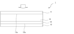
- FIG. 1 shows an embodiment of a photodiode type photodetector.
- the arrows in the figure represent the incident light on the photodetector.
- the photodetector 1 shown in FIG. 1 includes a lower electrode 12, an upper electrode 11 facing the lower electrode 12, a photoelectric conversion layer 13 provided between the lower electrode 12 and the upper electrode 11, the lower electrode 12, and the lower electrode 12. It includes a hole transport layer 14 provided between the photoelectric conversion layers 13.
- the photodetector 1 shown in FIG. 1 is used by injecting light from above the upper electrode 11.
- the photoelectric conversion layer 13 is a photoelectric conversion layer containing an aggregate of semiconductor quantum dots QD1 containing metal atoms and a ligand L1 coordinated to the semiconductor quantum dots QD1.
- the hole transport layer 14 is a hole transport layer containing an aggregate of semiconductor quantum dots QD2 containing a metal atom and a ligand L2 coordinated to the semiconductor quantum dots QD2.
- the optical path length L ⁇ satisfies the relationship of the following equation (1-1), and more preferably the relationship of the following equation (1-2) is satisfied.
- the wavelength ⁇ and the optical path length L ⁇ satisfy such a relationship, the light (incident light) incident from the upper electrode 11 side is reflected by the surface of the lower electrode 12 in the photoelectric conversion layer 13. It is possible to align the phase with the light (reflected light), and as a result, the light is strengthened by the optical interference effect, and higher external quantum efficiency can be obtained.
- ⁇ is the wavelength of the target light to be detected by the photodetector.
- L ⁇ is the optical path length of light having a wavelength ⁇ from the surface 12a on the photoelectric conversion layer 13 side of the lower electrode 12 to the surface 13a on the upper electrode layer side of the photoelectric conversion layer 13.
- m is an integer greater than or equal to 0.
- M is preferably an integer of 0 to 4, more preferably an integer of 0 to 3, and even more preferably an integer of 0 to 2. According to this aspect, the transport characteristics of charges such as holes and electrons are good, and the external quantum efficiency of the photodetector can be further enhanced.
- the optical path length means the product of the physical thickness of the substance through which light is transmitted and the refractive index.
- the photoelectric conversion layer 13 when the thickness of the photoelectric conversion layer is d 1 and the refractive index of the photoelectric conversion layer with respect to the wavelength ⁇ 1 is N 1 , the wavelength ⁇ 1 transmitted through the photoelectric conversion layer 13 The optical path length of light is N 1 ⁇ d 1 .
- the photoelectric conversion layer 13 and the hole transport layer 14 are composed of two or more laminated films, or when an intermediate layer exists between the hole transport layer 14 and the lower electrode 12, the optical path of each layer The integrated value of the length is the optical path length L ⁇ .
- the upper electrode 11 is preferably a transparent electrode formed of a conductive material that is substantially transparent to the wavelength of the target light detected by the photodetector.
- substantially transparent means that the light transmittance is 50% or more, preferably 60% or more, and particularly preferably 80% or more.
- the material of the upper electrode 11 include a conductive metal oxide. Specific examples include tin oxide, zinc oxide, indium oxide, indium tungsten oxide, indium zinc oxide (IZO), indium tin oxide (ITO), and fluorine-doped tin oxide (fluorine-topped). Tin oxide: FTO) and the like.
- the film thickness of the upper electrode 11 is not particularly limited, and is preferably 0.01 to 100 ⁇ m, more preferably 0.01 to 10 ⁇ m, and particularly preferably 0.01 to 1 ⁇ m.
- the thickness of each layer can be measured by observing the cross section of the light detection element 1 using a scanning electron microscope (SEM) or the like.
- Examples of the material forming the lower electrode 12 include metals such as platinum, gold, nickel, copper, silver, indium, ruthenium, palladium, rhodium, iridium, osnium, and aluminum, the above-mentioned conductive metal oxides, carbon materials, and the like. Examples include conductive polymers.
- the carbon material may be any material having conductivity, and examples thereof include fullerenes, carbon nanotubes, graphite, graphene and the like.
- the lower electrode 12 a thin film of metal or a conductive metal oxide (including a thin film formed by vapor deposition), or a glass substrate or a plastic substrate having this thin film is preferable.
- a glass substrate or the plastic substrate glass having a thin film of gold or platinum or glass on which platinum is vapor-deposited is preferable.
- the film thickness of the lower electrode 12 is not particularly limited, and is preferably 0.01 to 100 ⁇ m, more preferably 0.01 to 10 ⁇ m, and particularly preferably 0.01 to 1 ⁇ m.
- a transparent substrate may be arranged on the surface of the upper electrode 11 on the light incident side (the surface opposite to the photoelectric conversion layer 13 side).
- Examples of the type of transparent substrate include a glass substrate, a resin substrate, and a ceramic substrate.
- a blocking layer or the other hole transport layer described above may be provided between the hole transport layer 14 and the lower electrode 12. Further, a blocking layer or an electron transport layer may be provided between the photoelectric conversion layer 13 and the upper electrode 11.
- FIG. 2 shows another embodiment of the photodiode type photodetector.
- the photodetector element 1 shown in FIG. 2 is the same as the photodetector element 1 of the embodiment shown in FIG. 1 except that the hole transport layer 14 is provided between the upper electrode 11 and the photoelectric conversion layer 13.
- a transparent substrate may be arranged on the surface of the upper electrode 11 on the light incident side (the surface opposite to the hole transport layer 14 side).
- Examples of the type of transparent substrate include a glass substrate, a resin substrate, and a ceramic substrate.
- a blocking layer or the other hole transport layer described above may be provided between the hole transport layer 14 and the upper electrode 11.
- a blocking layer or an electron transport layer may be provided between the photoelectric conversion layer 13 and the lower electrode 12.
- the image sensor of the present invention includes the above-mentioned photodetector of the present invention.
- the configuration of the image sensor is not particularly limited as long as it includes the photodetector element of the present invention and functions as an image sensor.
- the image sensor of the present invention may include an infrared transmission filter layer.
- the infrared transmission filter layer preferably has low light transmittance in the visible wavelength band, and more preferably has an average transmittance of light in the wavelength range of 400 to 650 nm of 10% or less. It is more preferably 5.5% or less, and particularly preferably 5% or less.
- Examples of the infrared transmission filter layer include those made of a resin film containing a coloring material.
- Examples of the coloring material include chromatic color materials such as red color material, green color material, blue color material, yellow color material, purple color material, and orange color material, and black color material.
- the color material contained in the infrared transmission filter layer is preferably a combination of two or more kinds of chromatic color materials to form black or contains a black color material.
- Examples of the combination of the chromatic color materials in the case of forming black by the combination of two or more kinds of chromatic color materials include the following aspects (C1) to (C7).
- C2 An embodiment containing a red color material, a blue color material, and a yellow color material.
- C3 An embodiment containing a red color material, a blue color material, a yellow color material, and a purple color material.
- C4 An embodiment containing a red color material, a blue color material, a yellow color material, a purple color material, and a green color material.
- C5 An embodiment containing a red color material, a blue color material, a yellow color material, and a green color material.
- C6 An embodiment containing a red color material, a blue color material, and a green color material.
- C7 An embodiment containing a yellow color material and a purple color material.
- the chromatic color material may be a pigment or a dye. Pigments and dyes may be included.
- the black color material is preferably an organic black color material.
- examples of the organic black color material include bisbenzofuranone compounds, azomethine compounds, perylene compounds, and azo compounds.
- the infrared transmission filter layer may further contain an infrared absorber.
- infrared absorbers include pyrolopyrrole compounds, cyanine compounds, squarylium compounds, phthalocyanine compounds, naphthalocyanine compounds, quaterylene compounds, merocyanine compounds, croconium compounds, oxonor compounds, iminium compounds, dithiol compounds, triarylmethane compounds, pyromethene compounds, and azomethine compounds.
- examples thereof include compounds, anthraquinone compounds, dibenzofuranone compounds, dithiolene metal complexes, metal oxides, and metal boroides.
- the spectral characteristics of the infrared transmission filter layer can be appropriately selected according to the application of the image sensor.
- a filter layer satisfying any of the following spectral characteristics (1) to (5) can be mentioned.
- the maximum value of the light transmittance in the film thickness direction in the wavelength range of 400 to 750 nm is 20% or less (preferably 15% or less, more preferably 10% or less), and the light in the film thickness direction.
- the maximum value of the light transmittance in the film thickness direction in the wavelength range of 400 to 830 nm is 20% or less (preferably 15% or less, more preferably 10% or less), and the light in the film thickness direction.
- the maximum value of the light transmittance in the film thickness direction in the wavelength range of 400 to 950 nm is 20% or less (preferably 15% or less, more preferably 10% or less), and the light in the film thickness direction.
- the maximum value of the light transmittance in the film thickness direction in the wavelength range of 400 to 1100 nm is 20% or less (preferably 15% or less, more preferably 10% or less), and the wavelength range is 1400 to 1500 nm.
- a filter layer having a minimum value of 70% or more preferably 75% or more, more preferably 80% or more.
- the maximum value of the light transmittance in the film thickness direction in the wavelength range of 400 to 1300 nm is 20% or less (preferably 15% or less, more preferably 10% or less), and the wavelength range is 1600 to 2000 nm.
- a filter layer having a minimum value of 70% or more preferably 75% or more, more preferably 80% or more).
- infrared transmission filters Japanese Patent Application Laid-Open No. 2013-077009, Japanese Patent Application Laid-Open No. 2014-130173, Japanese Patent Application Laid-Open No. 2014-130338, International Publication No. 2015/166779, International Publication No. 2016/178346, International Publication No.
- the membranes described in 2016/190162, International Publication No. 2018/016232, JP-A-2016-177079, JP-A-2014-130332, and International Publication No. 2016/0277798 can be used.
- the infrared transmission filter may be used in combination of two or more filters, or a dual bandpass filter that transmits two or more specific wavelength regions with one filter may be used.
- the image sensor of the present invention may include an infrared shielding filter for the purpose of improving various performances such as noise reduction.
- the infrared shielding filter include, for example, International Publication No. 2016/186050, International Publication No. 2016/035695, Japanese Patent No. 6248945, International Publication No. 2019/021767, Japanese Patent Application Laid-Open No. 2017-06793, Patent. Examples thereof include the filters described in Japanese Patent Application Laid-Open No. 6506529.
- the image sensor of the present invention may include a dielectric multilayer film.
- the dielectric multilayer film include those in which a plurality of layers of a dielectric thin film having a high refractive index (high refractive index material layer) and a dielectric thin film having a low refractive index (low refractive index material layer) are alternately laminated.
- the number of laminated dielectric thin films in the dielectric multilayer film is not particularly limited, but is preferably 2 to 100 layers, more preferably 4 to 60 layers, and even more preferably 6 to 40 layers.
- As the material used for forming the high refractive index material layer a material having a refractive index of 1.7 to 2.5 is preferable.
- Specific examples include Sb 2 O 3 , Sb 2 S 3 , Bi 2 O 3 , CeO 2 , CeF 3 , HfO 2 , La 2 O 3 , Nd 2 O 3 , Pr 6 O 11 , Sc 2 O 3 , SiO. , Ta 2 O 5 , TiO 2 , TlCl, Y 2 O 3 , ZnSe, ZnS, ZrO 2, and the like.
- a material having a refractive index of 1.2 to 1.6 is preferable.
- the method for forming the dielectric multilayer film is not particularly limited, and for example, an ion plating method, a vacuum deposition method such as an ion beam, a physical vapor deposition method (PVD method) such as sputtering, or a chemical vapor deposition method. (CVD method) and the like.
- each of the high refractive index material layer and the low refractive index material layer is preferably 0.1 ⁇ to 0.5 ⁇ when the wavelength of the light to be blocked is ⁇ (nm).
- Specific examples of the dielectric multilayer film include the dielectric multilayer films described in JP-A-2014-130344 and JP-A-2018-010296.
- the dielectric multilayer film preferably has a transmission wavelength band in the infrared region (preferably a wavelength region having a wavelength of more than 700 nm, more preferably a wavelength region having a wavelength of more than 800 nm, and more preferably a wavelength region having a wavelength of more than 900 nm).
- the maximum transmittance in the transmission wavelength band is preferably 70% or more, more preferably 80% or more, and further preferably 90% or more.
- the maximum transmittance in the light-shielding wavelength band is preferably 20% or less, more preferably 10% or less, and further preferably 5% or less.
- the average transmittance in the transmission wavelength band is preferably 60% or more, more preferably 70% or more, and further preferably 80% or more.
- the wavelength range of the transmission wavelength band, when the center wavelength lambda t1 wavelengths showing a maximum transmittance is preferably the central wavelength lambda t1 ⁇ 100 nm, more preferably the central wavelength lambda t1 ⁇ 75 nm, It is more preferable that the center wavelength is ⁇ t1 ⁇ 50 nm.
- the dielectric multilayer film may have only one transmission wavelength band (preferably, a transmission wavelength band having a maximum transmittance of 90% or more), or may have a plurality of transmission wavelength bands.
- the image sensor of the present invention may include a color separation filter layer.
- the color separation filter layer include a filter layer including colored pixels.
- Examples of the types of colored pixels include red pixels, green pixels, blue pixels, yellow pixels, cyan pixels, magenta pixels, and the like.
- the color separation filter layer may include two or more colored pixels, or may have only one color. It can be appropriately selected according to the application and purpose.
- the color separation filter layer for example, the filter described in International Publication No. 2019/039172 can be used.
- the colored pixels of each color may be adjacent to each other, and a partition wall may be provided between the colored pixels.
- the material of the partition wall is not particularly limited. Examples thereof include organic materials such as siloxane resin and fluororesin, and inorganic particles such as silica particles.
- the partition wall may be made of a metal such as tungsten or aluminum.
- the image sensor of the present invention includes an infrared transmission filter layer and a color separation layer
- the color separation layer is provided on an optical path different from the infrared transmission filter layer. It is also preferable that the infrared transmission filter layer and the color separation layer are arranged two-dimensionally. The fact that the infrared transmission filter layer and the color separation layer are two-dimensionally arranged means that at least a part of both is present on the same plane.
- the image sensor of the present invention may include an intermediate layer such as a flattening layer, a base layer, and an adhesion layer, an antireflection film, and a lens.
- an antireflection film for example, a film prepared from the composition described in International Publication No. 2019/017280 can be used.
- the lens for example, the structure described in International Publication No. 2018/092600 can be used.
- the photodetector of the present invention has excellent sensitivity to light having a wavelength in the infrared region. Therefore, the image sensor of the present invention can be preferably used as an infrared image sensor. Further, the image sensor of the present invention can be preferably used as a sensor for sensing light having a wavelength of 900 to 2000 nm, and more preferably as a sensor for sensing light having a length of 900 to 1600 nm.
- Dispersion liquid 1 of PbS quantum dots A precursor solution was obtained by measuring 6.74 mL of oleic acid, 6.3 mmol of lead oxide and 30 mL of octadecene in a flask and heating at 120 ° C. under vacuum for 100 minutes. The temperature of the solution was then adjusted to 100 ° C., then the system was placed in a nitrogen flow state and then 2.5 mmol of hexamethyldisiratene was injected with 5 mL of octadecene.
- the obtained PbS quantum dot dispersion 1 was estimated from light absorption measurements in the visible to infrared region using an ultraviolet-visible near-infrared spectrophotometer (V-670, manufactured by JASCO Corporation). The bandgap of was approximately 1.35 eV.
- Example 1 A titanium oxide film was formed on a quartz glass substrate with an indium tin oxide film by 50 nm sputtering. Next, the dispersion liquid 1 of the PbS quantum dots was dropped onto the titanium oxide film formed on the substrate and spin-coated at 2500 rpm to form a PbS quantum dot aggregate film (step PC1). Next, a methanol solution of zinc iodide 25 mmol / L and a methanol solution of 3-mercaptopropionic acid 0.01% by volume were added dropwise onto the PbS quantum dot aggregate membrane as a ligand solution, and then allowed to stand for 1 minute.
- step PC2 Photoelectric conversion is a PbS quantum dot aggregate membrane in which the ligand is exchanged from oleic acid to 3-mercaptopropionic acid and zinc iodide by repeating the operation of process PC1 and process PC2 as one cycle for 10 cycles.
- the layer was formed to a thickness of 200 nm.
- step HT1 the above-mentioned dispersion liquid 3 of PbS quantum dots was dropped onto the photoelectric conversion layer and spin-coated at 2500 rpm to form a PbS quantum dot aggregate film.
- step HT2 a 0.01% by volume methanol solution of ethanedithiol was added dropwise as a ligand solution, and the mixture was allowed to stand for 1 minute and spin-dried at 2500 rpm.
- acetonitrile was dropped onto the PbS quantum dot aggregate film, spin-dried at 2500 rpm for 20 seconds, and the ligand coordinated to the PbS quantum dot was exchanged from oleic acid to ethanedithiol (. Process HT2).
- step HT1 and step HT2 were repeated for two cycles, and the hole transport layer, which is a PbS quantum dot aggregate membrane in which the ligand was exchanged from oleic acid to ethanedithiol, had a thickness of 40 nm. Formed in.
- gold was formed on the hole transport layer by vapor deposition to a thickness of 100 nm to obtain a photodiode-type photodetector.
- Example 1 A photodiode-type photodetector was obtained in the same manner as in Example 1 except that the dispersion liquid 1 of PbS quantum dots was used instead of the dispersion liquid 3 of PbS quantum dots in the step HT1.
- the external quantum efficiency (EQE) and dark current of the manufactured photodetector were measured using a semiconductor parameter analyzer (C4156, manufactured by Agilent).
- IV characteristic the current-voltage characteristic
- the IV characteristics were measured while sweeping the voltage from 0 V to -5 V while irradiating with monochrome light of 940 nm.
- the external quantum efficiency (EQE) was calculated from the photocurrent value when -2V was applied. The smaller the value, the better the dark current.
- the photodetector of the example had a lower dark current than that of the comparative example 1.
- Example 2 A photodiode-type photodetector was obtained in the same manner as in Example 1 except that the dispersion liquid 2 of PbS quantum dots was used instead of the dispersion liquid 3 of PbS quantum dots in the step HT1.
- Example 3 A photodiode-type photodetector was obtained in the same manner as in Example 1 except that a methanol solution of tetrabutylammonium iodide 25 mmol / L was used as the ligand solution in step PC2.
- Example 4 A photodiode-type photodetector was obtained in the same manner as in Example 1 except that a methanol solution of 0.01% by volume of thioglycolic acid was used as the ligand solution in step HT2.
- Example 5 A photodiode-type photodetector was obtained in the same manner as in Example 1 except that a methanol solution of lead chloride 25 mmol / L and a methanol solution of ethanedithiol 0.01% by volume were used as the ligand solution in step HT2. rice field.
- the dark current was lower in the photodetector elements of Examples 2 to 5 than in Comparative Example 1. Further, the photodetector elements of Examples 2 to 5 had the same external quantum efficiency as the photodetector elements of Example 1.
- an image sensor was prepared by a known method together with an optical filter prepared according to the methods described in International Publication No. 2016/186050 and International Publication No. 2016/190162, and solidified. By incorporating it into an image sensor, an image sensor having good visibility-infrared imaging performance can be obtained.
- the same effect can be obtained by changing the semiconductor quantum dots of the photoelectric conversion layer and the hole transport layer to PbSe quantum dots.
- Photodetection element 11 Upper electrode 12: Lower electrode 13: Photoelectric conversion layer 14: Hole transport layer
Landscapes
- Chemical & Material Sciences (AREA)
- Inorganic Chemistry (AREA)
- Engineering & Computer Science (AREA)
- Materials Engineering (AREA)
- Organic Chemistry (AREA)
- Crystallography & Structural Chemistry (AREA)
- Nanotechnology (AREA)
- Physics & Mathematics (AREA)
- Electromagnetism (AREA)
- Light Receiving Elements (AREA)
- Solid State Image Pick-Up Elements (AREA)
- Transforming Light Signals Into Electric Signals (AREA)
Priority Applications (4)
| Application Number | Priority Date | Filing Date | Title |
|---|---|---|---|
| KR1020227026904A KR102809886B1 (ko) | 2020-02-13 | 2021-02-08 | 광검출 소자 및 이미지 센서 |
| JP2022500385A JP7352717B2 (ja) | 2020-02-13 | 2021-02-08 | 光検出素子およびイメージセンサ |
| CN202180013673.9A CN115104189B (zh) | 2020-02-13 | 2021-02-08 | 光检测元件及图像传感器 |
| US17/882,621 US12446388B2 (en) | 2020-02-13 | 2022-08-08 | Photodetector element and image sensor |
Applications Claiming Priority (2)
| Application Number | Priority Date | Filing Date | Title |
|---|---|---|---|
| JP2020022575 | 2020-02-13 | ||
| JP2020-022575 | 2020-02-13 |
Related Child Applications (1)
| Application Number | Title | Priority Date | Filing Date |
|---|---|---|---|
| US17/882,621 Continuation US12446388B2 (en) | 2020-02-13 | 2022-08-08 | Photodetector element and image sensor |
Publications (1)
| Publication Number | Publication Date |
|---|---|
| WO2021161938A1 true WO2021161938A1 (ja) | 2021-08-19 |
Family
ID=77292222
Family Applications (1)
| Application Number | Title | Priority Date | Filing Date |
|---|---|---|---|
| PCT/JP2021/004475 Ceased WO2021161938A1 (ja) | 2020-02-13 | 2021-02-08 | 光検出素子およびイメージセンサ |
Country Status (6)
| Country | Link |
|---|---|
| US (1) | US12446388B2 (https=) |
| JP (1) | JP7352717B2 (https=) |
| KR (1) | KR102809886B1 (https=) |
| CN (1) | CN115104189B (https=) |
| TW (1) | TWI886210B (https=) |
| WO (1) | WO2021161938A1 (https=) |
Cited By (3)
| Publication number | Priority date | Publication date | Assignee | Title |
|---|---|---|---|---|
| WO2023288288A1 (en) | 2021-07-15 | 2023-01-19 | Turn Biotechnologies, Inc. | Synthetic, persistent rna constructs with on/off mechanism for controlled expression and methods of use |
| WO2023288287A2 (en) | 2021-07-15 | 2023-01-19 | Turn Biotechnologies, Inc. | Synthetic, persistent rna constructs and methods of use for cell rejuvenation and for treatment |
| WO2025063060A1 (ja) * | 2023-09-20 | 2025-03-27 | 富士フイルム株式会社 | 半導体膜、光検出素子およびイメージセンサ |
Families Citing this family (1)
| Publication number | Priority date | Publication date | Assignee | Title |
|---|---|---|---|---|
| KR20250008602A (ko) * | 2023-07-06 | 2025-01-15 | 삼성디스플레이 주식회사 | 양자점 복합체, 양자점 복합체를 포함하는 발광 소자, 및 양자점 복합체를 포함하는 표시 장치 |
Citations (7)
| Publication number | Priority date | Publication date | Assignee | Title |
|---|---|---|---|---|
| JP2009513018A (ja) * | 2005-10-20 | 2009-03-26 | ザ リージェンツ オブ ザ ユニバーシティ オブ カリフォルニア | 溶液から調製されるナノクリスタル太陽電池 |
| JP2014093327A (ja) * | 2012-10-31 | 2014-05-19 | Fujifilm Corp | 半導体膜、半導体膜の製造方法、太陽電池、発光ダイオード、薄膜トランジスタ、および、電子デバイス |
| JP2015537378A (ja) * | 2012-10-26 | 2015-12-24 | リサーチ トライアングル インスティテュート | 溶液プロセスによる量子ドットを利用した中間帯半導体、ヘテロ接合、及び光電子デバイス、並びに関連する方法 |
| US20170062139A1 (en) * | 2015-08-31 | 2017-03-02 | The University Of Akron | Photodetector utilizing quantum dots and perovskite hybrids as light harvesters |
| US20180254421A1 (en) * | 2015-10-02 | 2018-09-06 | Toyota Motor Europe | All quantum dot based optoelectronic device |
| JP2018529214A (ja) * | 2015-06-11 | 2018-10-04 | ユニバーシティー オブ フロリダ リサーチ ファウンデーション, インコーポレイテッドUniversity Of Florida Research Foundation, Inc. | 単分散ir吸収ナノ粒子及び関連する方法及びデバイス |
| WO2019150989A1 (ja) * | 2018-01-31 | 2019-08-08 | ソニー株式会社 | 光電変換素子および撮像装置 |
Family Cites Families (3)
| Publication number | Priority date | Publication date | Assignee | Title |
|---|---|---|---|---|
| JP5488595B2 (ja) * | 2009-05-22 | 2014-05-14 | コニカミノルタ株式会社 | 有機光電変換素子 |
| WO2015031835A1 (en) * | 2013-08-29 | 2015-03-05 | University Of Florida Research Foundation, Inc. | Air stable infrared photodetectors from solution-processed inorganic semiconductors |
| US9318632B2 (en) * | 2013-11-14 | 2016-04-19 | University Of South Florida | Bare quantum dots superlattice photonic devices |
-
2021
- 2021-02-05 TW TW110104510A patent/TWI886210B/zh active
- 2021-02-08 WO PCT/JP2021/004475 patent/WO2021161938A1/ja not_active Ceased
- 2021-02-08 KR KR1020227026904A patent/KR102809886B1/ko active Active
- 2021-02-08 CN CN202180013673.9A patent/CN115104189B/zh active Active
- 2021-02-08 JP JP2022500385A patent/JP7352717B2/ja active Active
-
2022
- 2022-08-08 US US17/882,621 patent/US12446388B2/en active Active
Patent Citations (7)
| Publication number | Priority date | Publication date | Assignee | Title |
|---|---|---|---|---|
| JP2009513018A (ja) * | 2005-10-20 | 2009-03-26 | ザ リージェンツ オブ ザ ユニバーシティ オブ カリフォルニア | 溶液から調製されるナノクリスタル太陽電池 |
| JP2015537378A (ja) * | 2012-10-26 | 2015-12-24 | リサーチ トライアングル インスティテュート | 溶液プロセスによる量子ドットを利用した中間帯半導体、ヘテロ接合、及び光電子デバイス、並びに関連する方法 |
| JP2014093327A (ja) * | 2012-10-31 | 2014-05-19 | Fujifilm Corp | 半導体膜、半導体膜の製造方法、太陽電池、発光ダイオード、薄膜トランジスタ、および、電子デバイス |
| JP2018529214A (ja) * | 2015-06-11 | 2018-10-04 | ユニバーシティー オブ フロリダ リサーチ ファウンデーション, インコーポレイテッドUniversity Of Florida Research Foundation, Inc. | 単分散ir吸収ナノ粒子及び関連する方法及びデバイス |
| US20170062139A1 (en) * | 2015-08-31 | 2017-03-02 | The University Of Akron | Photodetector utilizing quantum dots and perovskite hybrids as light harvesters |
| US20180254421A1 (en) * | 2015-10-02 | 2018-09-06 | Toyota Motor Europe | All quantum dot based optoelectronic device |
| WO2019150989A1 (ja) * | 2018-01-31 | 2019-08-08 | ソニー株式会社 | 光電変換素子および撮像装置 |
Non-Patent Citations (3)
| Title |
|---|
| MARCUS L. BÖHM, TOM C. JELLICOE, JASMINE P.H. RIVETT, ADITYA SADHANALA, NATHANIEL J.L.K. DAVIS, FREDERIK S.F. MORGENSTERN, KARL C.: "Size and Energy Level Tuning of Quantum Dot Solids via a Hybrid Ligand Complex", JOURNAL OF PHYSICAL CHEMISTRY LETTERS, vol. 6, no. 17, 3 September 2015 (2015-09-03), US, pages 3510 - 3514, XP055766549, ISSN: 1948-7185, DOI: 10.1021/acs.jpclett.5b01751 * |
| PRADHAN SANTANU, STAVRINADIS ALEXANDROS, GUPTA SHUCHI, BI YU, DI STASIO FRANCESCO, KONSTANTATOS GERASIMOS: "Trap-State Suppression and improved Charge Transport in PbS Quantum Dot Solar Cells with Synergistic Mixed-Ligand Treatments", SMALL, vol. 13, no. 21, 12 April 2017 (2017-04-12), 20170601, pages 1 - 9, XP055782946, ISSN: 1613-6810, DOI: 10.1002/smll.201700598 * |
| XU JUNFENG, WANG HAOWEI, YANG SHENGYI, NI GUOQIANG, ZOU BINGSUO: "High-sensitivity broadband colloidal quantum dot heterojunction photodetector for night-sky radiation", JOURNAL OF ALLOYS AND COMPOUNDS, vol. 764, 1 October 2018 (2018-10-01), pages 446 - 451, XP055847810, ISSN: 0925-8388, DOI: 10.1016/j.jallcom.2018.06.105 * |
Cited By (3)
| Publication number | Priority date | Publication date | Assignee | Title |
|---|---|---|---|---|
| WO2023288288A1 (en) | 2021-07-15 | 2023-01-19 | Turn Biotechnologies, Inc. | Synthetic, persistent rna constructs with on/off mechanism for controlled expression and methods of use |
| WO2023288287A2 (en) | 2021-07-15 | 2023-01-19 | Turn Biotechnologies, Inc. | Synthetic, persistent rna constructs and methods of use for cell rejuvenation and for treatment |
| WO2025063060A1 (ja) * | 2023-09-20 | 2025-03-27 | 富士フイルム株式会社 | 半導体膜、光検出素子およびイメージセンサ |
Also Published As
| Publication number | Publication date |
|---|---|
| KR102809886B1 (ko) | 2025-05-19 |
| US12446388B2 (en) | 2025-10-14 |
| KR20220124220A (ko) | 2022-09-13 |
| TW202135333A (zh) | 2021-09-16 |
| TWI886210B (zh) | 2025-06-11 |
| CN115104189B (zh) | 2024-12-10 |
| US20220384753A1 (en) | 2022-12-01 |
| CN115104189A (zh) | 2022-09-23 |
| JPWO2021161938A1 (https=) | 2021-08-19 |
| JP7352717B2 (ja) | 2023-09-28 |
Similar Documents
| Publication | Publication Date | Title |
|---|---|---|
| US12415953B2 (en) | Photodetector element and image sensor | |
| JP7352717B2 (ja) | 光検出素子およびイメージセンサ | |
| US12404450B2 (en) | Photodetector element, manufacturing method for photodetector element, image sensor, dispersion liquid, and semiconductor film | |
| JP7372452B2 (ja) | 光電変換膜、分散液、光検出素子およびイメージセンサ | |
| WO2021251309A1 (ja) | 半導体膜、半導体膜の製造方法、光検出素子およびイメージセンサ | |
| US20220406850A1 (en) | Photodetector element and image sensor | |
| US20250304800A1 (en) | Dispersion liquid, photoelectric conversion film, method for manufacturing photoelectric conversion film, photodetector, and image sensor | |
| US12384962B2 (en) | Photodetector element, manufacturing method for photodetector element, and image sensor | |
| US20220115611A1 (en) | Photodetector element, manufacturing method for photodetector element, image sensor, dispersion liquid, and semiconductor film | |
| US20220102420A1 (en) | Manufacturing method for semiconductor film, photoelectric conversion element, image sensor, and semiconductor film | |
| WO2021161940A1 (ja) | 半導体膜、光検出素子、イメージセンサおよび半導体膜の製造方法 | |
| JP7405850B2 (ja) | 半導体膜、光電変換素子、イメージセンサおよび半導体膜の製造方法 | |
| WO2023008353A1 (ja) | 光検出素子およびイメージセンサ | |
| WO2022264872A1 (ja) | 光検出素子およびイメージセンサ |
Legal Events
| Date | Code | Title | Description |
|---|---|---|---|
| 121 | Ep: the epo has been informed by wipo that ep was designated in this application |
Ref document number: 21753866 Country of ref document: EP Kind code of ref document: A1 |
|
| ENP | Entry into the national phase |
Ref document number: 2022500385 Country of ref document: JP Kind code of ref document: A |
|
| ENP | Entry into the national phase |
Ref document number: 20227026904 Country of ref document: KR Kind code of ref document: A |
|
| NENP | Non-entry into the national phase |
Ref country code: DE |
|
| 122 | Ep: pct application non-entry in european phase |
Ref document number: 21753866 Country of ref document: EP Kind code of ref document: A1 |
|
| WWC | Wipo information: continuation of processing after refusal or withdrawal |
Ref document number: 1020227026904 Country of ref document: KR |