WO2021157629A1 - 電子装置 - Google Patents
電子装置 Download PDFInfo
- Publication number
- WO2021157629A1 WO2021157629A1 PCT/JP2021/003999 JP2021003999W WO2021157629A1 WO 2021157629 A1 WO2021157629 A1 WO 2021157629A1 JP 2021003999 W JP2021003999 W JP 2021003999W WO 2021157629 A1 WO2021157629 A1 WO 2021157629A1
- Authority
- WO
- WIPO (PCT)
- Prior art keywords
- electronic component
- mounted member
- fill
- electronic device
- solder
- Prior art date
- Legal status (The legal status is an assumption and is not a legal conclusion. Google has not performed a legal analysis and makes no representation as to the accuracy of the status listed.)
- Ceased
Links
Images


Classifications
-
- H—ELECTRICITY
- H05—ELECTRIC TECHNIQUES NOT OTHERWISE PROVIDED FOR
- H05K—PRINTED CIRCUITS; CASINGS OR CONSTRUCTIONAL DETAILS OF ELECTRIC APPARATUS; MANUFACTURE OF ASSEMBLAGES OF ELECTRICAL COMPONENTS
- H05K3/00—Apparatus or processes for manufacturing printed circuits
- H05K3/30—Assembling printed circuits with electric components, e.g. with resistors
- H05K3/32—Assembling printed circuits with electric components, e.g. with resistors electrically connecting electric components or wires to printed circuits
- H05K3/34—Assembling printed circuits with electric components, e.g. with resistors electrically connecting electric components or wires to printed circuits by soldering
- H05K3/341—Surface mounted components
- H05K3/3431—Leadless components
-
- G—PHYSICS
- G01—MEASURING; TESTING
- G01C—MEASURING DISTANCES, LEVELS OR BEARINGS; SURVEYING; NAVIGATION; GYROSCOPIC INSTRUMENTS; PHOTOGRAMMETRY OR VIDEOGRAMMETRY
- G01C19/00—Gyroscopes; Turn-sensitive devices using vibrating masses; Turn-sensitive devices without moving masses; Measuring angular rate using gyroscopic effects
- G01C19/56—Turn-sensitive devices using vibrating masses, e.g. vibratory angular rate sensors based on Coriolis forces
- G01C19/5783—Mountings or housings not specific to any of the devices covered by groups G01C19/5607 - G01C19/5719
-
- H—ELECTRICITY
- H05—ELECTRIC TECHNIQUES NOT OTHERWISE PROVIDED FOR
- H05K—PRINTED CIRCUITS; CASINGS OR CONSTRUCTIONAL DETAILS OF ELECTRIC APPARATUS; MANUFACTURE OF ASSEMBLAGES OF ELECTRICAL COMPONENTS
- H05K1/00—Printed circuits
- H05K1/18—Printed circuits structurally associated with non-printed electric components
- H05K1/181—Printed circuits structurally associated with non-printed electric components associated with surface mounted components
-
- H—ELECTRICITY
- H05—ELECTRIC TECHNIQUES NOT OTHERWISE PROVIDED FOR
- H05K—PRINTED CIRCUITS; CASINGS OR CONSTRUCTIONAL DETAILS OF ELECTRIC APPARATUS; MANUFACTURE OF ASSEMBLAGES OF ELECTRICAL COMPONENTS
- H05K2201/00—Indexing scheme relating to printed circuits covered by H05K1/00
- H05K2201/10—Details of components or other objects attached to or integrated in a printed circuit board
- H05K2201/10007—Types of components
- H05K2201/10151—Sensor
-
- H—ELECTRICITY
- H05—ELECTRIC TECHNIQUES NOT OTHERWISE PROVIDED FOR
- H05K—PRINTED CIRCUITS; CASINGS OR CONSTRUCTIONAL DETAILS OF ELECTRIC APPARATUS; MANUFACTURE OF ASSEMBLAGES OF ELECTRICAL COMPONENTS
- H05K2201/00—Indexing scheme relating to printed circuits covered by H05K1/00
- H05K2201/10—Details of components or other objects attached to or integrated in a printed circuit board
- H05K2201/10613—Details of electrical connections of non-printed components, e.g. special leads
- H05K2201/10954—Other details of electrical connections
- H05K2201/10977—Encapsulated connections
Definitions
- the present disclosure relates to an electronic device in which an electronic component is arranged on a mounted member via solder.
- the mounted member is composed of, for example, a printed circuit board or the like.
- the electronic component is composed of a QFN (abbreviation of Quad Flat No leaded package) having a plurality of electrodes on the back surface side, and has a rectangular parallelepiped outer shape.
- a plurality of electrodes are connected to the mounted member via solder.
- a side fill that mechanically connects the electronic component and the mounted member is arranged around the solder so as to reduce the stress applied to the solder and extend the life of the solder. ing. More specifically, the side fill of the electronic device is arranged so as to cover the corner portion of the electronic component in the normal direction with respect to the surface direction of the mounted member.
- the side fill is arranged so as to cover the corners of the electronic component in the normal direction.
- the side fill is arranged up to the corner of the electronic component on the side opposite to the mounted member side, the stress generated due to the side fill tends to increase at the corner of the electronic component, which is generated in the electronic component. Moment tends to increase. Therefore, there is a possibility that a defect may occur in the electronic component.
- the purpose of this disclosure is to provide an electronic device in which defects of electronic components are less likely to occur.
- an electronic device has a mounted member having one surface and an outer shape having a rectangular shape, and a plurality of electrodes are formed on a surface facing one surface of the mounted member and arranged on one surface.
- the electronic component is placed between the electrode and the mounted member of the electronic component, the solder that electrically and mechanically connects the electrode and the mounted member, and the solder that is placed around the solder, and the electronic component and the mounted member are mounted.
- a side fill for mechanically connecting the mounting member is provided, and the side fill is arranged so that the corner portion of the electronic component on the side opposite to the mounted member side is exposed.
- the stress generated in the corners of the electronic component due to the side fill is larger than that in the case where the corners of the electronic component on the opposite side to the mounted member side are covered with the side fill. It is possible to suppress the increase of the moment generated in the electronic component. Therefore, it is possible to suppress the occurrence of defects in the electronic components.
- the electronic device of the first embodiment will be described with reference to the drawings.
- an electronic device constituting a self-position estimation system including GNSS (abbreviation of Global Navigation Satellite System) and IMU (abbreviation of Inertial Measurement Unit) will be described.
- the electronic device of the present embodiment is, for example, a vehicle equipped with a level 3 or higher driving support device at the level of automation defined by the Japanese government or the National Highway Traffic Safety Administration (NHTSA). It is suitable to be mounted on.
- GNSS abbreviation of Global Navigation Satellite System
- IMU abbreviation of Inertial Measurement Unit
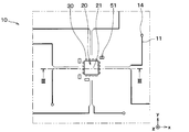
- the electronic device has a configuration in which the electronic component 20 is arranged on the printed circuit board 10 as the mounted member.
- the insulating film 15 and the side fill 40 which will be described later, are omitted, and the wiring pattern 11 and the like covered with the insulating film 15 are also shown by solid lines.
- the cross-sectional structure of the electronic component 20 is shown in a simplified manner.
- one direction in the plane direction of the printed substrate 10 is the x-axis direction
- the direction orthogonal to the x-axis direction in the plane direction is the y-axis direction
- the x-axis direction and the direction orthogonal to the y-axis direction are the z-axis.
- the wiring pattern 11 and the land 11a connected to the wiring pattern 11 are formed on the one side 10a side, the wiring pattern 12 is formed on the other side 10b side, and the wiring layer 13 is formed inside. It is a formed multilayer wiring board.
- the wiring pattern 11 formed on the one side 10a side, the wiring pattern 12 formed on the other side 10b side, and the wiring layer 13 formed inside are appropriately connected via the through via 14.
- such a printed circuit board 10 is constructed by using, for example, a glass epoxy board or the like.
- the insulating film 15 is formed on the one side 10a side, and the insulating film 16 is formed on the other side 10b side.
- the insulating films 15 and 16 are each made of a solder resist or the like.
- a contact hole 15a that exposes the land 11a connected to the electronic component 20 is formed in the insulating film 15 formed on the one side 10a side.
- the wiring pattern 11 formed around the electronic component 20 is omitted in the normal direction (that is, the z-axis direction) with respect to the surface direction of the printed circuit board 10.
- the wiring pattern 11 is formed so as to be connected to the land 11a to which the electronic component 20 is connected.
- the electronic component 20 is configured to include an inertial force sensor that detects an inertial force.
- the electronic component 20 includes an acceleration sensor that detects acceleration in the x-axis direction, an acceleration sensor that detects acceleration in the y-axis direction, and an acceleration sensor that detects acceleration in the z-axis direction.
- the electronic component 20 includes an angular velocity sensor that detects an angular velocity around the x-axis direction, an angular velocity sensor that detects an angular velocity around the y-axis direction, and an angular velocity sensor that detects an angular velocity around the z-axis direction.
- the electronic component 20 of this embodiment is a so-called IMU.
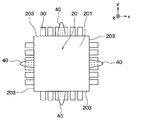
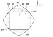
- the electronic component 20 of the present embodiment is QFN, although the specific configuration is omitted, and each acceleration sensor and each angular velocity sensor are housed in the case 21.
- the case 21 has a rectangular parallelepiped outer shape, and has four side surfaces 203 connecting one side 201, one side 201 and the other side 202 on the opposite side, and one side 201 and the other side 202.
- the rectangular parallelepiped shape here also includes a cube shape. Further, the rectangular parallelepiped shape here means a slight curvature at a corner portion that is an intersection of one side surface 201 and two adjacent side surfaces 203, a corner portion that is an intersection of two side surfaces 203 adjacent to another surface 202, and the like. It includes those in which parts are formed.
- a plurality of electrodes 22 electrically connected to each acceleration sensor and each angular velocity sensor housed in the case 21 are formed on a surface including the other surface 202.
- the plurality of electrodes 22 are formed so as to extend from each side surface 203 to the other surface 202, respectively.
- the land 11a formed on the printed circuit board 10 and each electrode 22 are electrically and mechanically connected via the solder 30.
- the electronic component 20 is arranged so that each side surface 203 is parallel to the x-axis direction or the y-axis direction.
- a side fill 40 made of an epoxy resin is arranged so as to mechanically connect the printed circuit board 10 and the electronic component 20. That is, the electronic component 20 is mechanically connected to the printed circuit board 10 via the solder 30 and the side fill 40.
- FIG. 5 is a schematic view of the electronic component 20 as viewed from the normal direction with respect to one of the side surfaces 203, but the printed circuit board 10 is shown as a cross-sectional view of a portion corresponding to the one side surface 203. Further, in FIG. 5, the solder 30 arranged between each electrode 22 and the land 11a is omitted.
- four side fills 40 are arranged so as to be mechanically connected to each side surface 203 of the electronic component 20 in the z-axis direction, and the four side fills 40 are arranged apart from each other. ing.
- the electronic component 20 in the electronic component 20, six electrodes 22 are arranged from each side surface 203 to the other surface 202, and the solder 30 is arranged so as to be connected to each electrode 22.
- the width direction is defined as the direction along the surface direction of one surface 10a of the printed circuit board 10 on the side surface 203.
- the width direction can be said to be the direction along the boundary line between the one side surface 201 and the other side surface 202 on the side surface 203, and is the left-right direction on the paper surface in FIG.
- the side fill 40 of the present embodiment exposes the solder 30 connected to the electrodes 22 at both ends in the width direction, and covers the solder 30 connected to the electrodes 22 at the inner edge in the width direction. It is arranged in a portion located between the solders 30.
- the side fill 40 is arranged so as to spread in the width direction in the normal direction with respect to the side surface 203 of the case 21.
- the side fill 40 has a mountain shape in which the height from the printed circuit board 10 (hereinafter, also simply referred to as the height) is lower than the portion where both ends in the width direction are located on the inner edge side.
- the side fill 40 has a length w1 between the highest height portion and one end portion in the normal direction with respect to the side surface 203, and the highest height portion and the other end portion. The length between them is equal to w2. That is, the height of the portion of the side fill 40 located at the center in the width direction is the highest.
- the length w1 and the length w2 of the side fill 40 may be different. That is, the height of the portion of the side fill 40 different from the center in the width direction may be the highest.
- each side fill 40 is arranged so as to be point-symmetric with respect to the center of the electronic component 20. Further, each side fill 40 is arranged so as to pass through the center of the electronic component 20 and be line-symmetric with respect to the virtual line extending in the x-axis direction and line-symmetrically with respect to the virtual line extending in the y-axis direction. ing.
- the side fill 40 is arranged so that the corner portion (hereinafter, also simply referred to as the upper end corner portion) C1 of the electronic component 20 on the side opposite to the printed circuit board 10 side is exposed.
- the side fill 40 connected to each side surface 203 is arranged so as to expose the solder 30 connected to the electrodes 22 at both ends in the width direction as described above.
- the side fill 40 is arranged so that the corner portion (hereinafter, simply referred to as the lower end corner portion) C2 on the printed circuit board 10 side of the electronic component 20 is also exposed.
- the upper end corner portion C1 can be said to be an intersection of one side surface 201 and two adjacent side surfaces 203.
- the lower end corner portion C2 can be said to be the intersection of the other surface 202 and the two adjacent side surfaces 203.
- the printed circuit board 10 is connected to external electronic components 51 such as chip resistors and chip capacitors, a microcomputer 52, GNSS components 53, and other circuit units. Socket 54 and the like are mounted. Further, the printed circuit board 10 is formed with a screw hole 17 or the like at the outer edge portion through which a screw for screw-fixing the printed circuit board 10 is inserted into a housing made of an aluminum alloy or the like.
- the above is the configuration of the electronic device in this embodiment.
- such an electronic device is screwed to the housing by inserting a screw into a screw hole 17 formed in the printed circuit board 10, and a metal lid portion accommodates the electronic device.
- a metal lid portion accommodates the electronic device.
- the in-vehicle mounted component By being provided on the body, it constitutes an in-vehicle mounted component.
- the in-vehicle mounted parts are mounted on the vehicle by mechanically fixing the housing, and are used to execute various controls of the vehicle.
- the printed circuit board 10 may warp when the electronic device is fixed to the housing or when the vehicle-mounted component is mounted on the vehicle after the vehicle-mounted component is configured. That is, the electronic device of the present embodiment is configured by arranging the electronic components 20 on the printed circuit board 10 where warpage may occur.
- the life of the solder 30 can be extended.
- the side fill 40 is arranged so as to expose the upper end corner portion C1 of the electronic component 20. Therefore, the stress that can be generated in the upper end corner C1 of the electronic component 20 is larger than that in the case where the upper end corner C1 of the electronic component 20 is covered with the side fill 40, such as when the printed circuit board 10 is warped. It is possible to suppress the increase of the moment generated in the electronic component 20. Therefore, it is possible to suppress the occurrence of defects in the electronic components.
- the electronic component 20 is an IMU, and when the moment generated in the electronic component 20 becomes large, problems such as 0-point fluctuation and axis misalignment are likely to occur.
- the side fill 40 is arranged as described above, it is possible to suppress the occurrence of problems such as 0-point fluctuation and axis misalignment. That is, according to the electronic device of the present embodiment, the robustness of the electronic component 20 can be improved, and the deterioration of the detection accuracy of the IMU can be suppressed. Further, since it is difficult for the electronic component 20 to fluctuate at 0 points, it is not necessary to perform 0 point correction after assembling the electronic device, and it is possible to reduce the adjustment cost and the inspection cost.
- each side fill 40 has a mountain shape in which the height of the end portion in the width direction is lower than the height of the inner edge portion. Therefore, for example, as compared with the case where the height of the side fill 40 is constant along the width direction, it is not necessary to strictly control the shape of the side fill 40, and the manufacturing process can be simplified. Can be done.
- the side fill 40 is arranged point-symmetrically with respect to the center of the electronic component 20. Further, the side fill 40 is arranged so as to pass through the center of the electronic component 20 and be line-symmetric with respect to the virtual line extending in the x-axis direction and line-symmetrically with respect to the virtual line extending in the y-axis direction. There is. Therefore, the stress propagated from each side fill 40 to the electronic component 20 can be easily made uniform. That is, it becomes easy to maintain the balance of stress due to the side fill 40. Therefore, it is possible to further suppress the occurrence of defects in the electronic component 20.
- the electronic component 20 is an IMU, and it is used to configure a self-position estimation system. Then, as described above, the electronic component 20 is in a state where the inertial force of the 6 axes can be detected with high accuracy because the deviation in the axial direction is suppressed and the occurrence of 0-point fluctuation is suppressed. ing. Therefore, the electronic device of the present embodiment can realize dead reckoning (that is, inertial navigation) of the vehicle for a long time.
- the life of the solder 30 can be extended.
- the portion where the printed circuit board 10 and the electronic component 20 are mechanically connected increases. Therefore, for example, when the printed circuit board 10 is warped, electrons are emitted from the printed circuit board 10. The stress propagated to the component 20 increases.
- the amount of arrangement of the side fill 40 increases, so that the maximum tensile stress applied to the solder 30 decreases. Therefore, as the amount of the side fill 40 arranged is increased, the life of the solder 30 can be extended.
- the amount of the side fill 40 arranged here is the amount of the portion that mechanically connects the printed circuit board 10 and the electronic component 20. Then, increasing the arrangement amount of the side fill 40 means increasing the number of portions that mechanically connect the printed circuit board 10 and the electronic component 20.
- the side fill 40 has the above configuration and the arrangement amount is set according to the application.
- each side fill 40 may be arranged as shown in FIGS. 8A-8C. That is, each side fill 40 is connected to the two electrodes 22 at the inner edge in the width direction while exposing the solder 30 connected to the two electrodes 22 at both ends in the width direction in the normal direction with respect to the printed circuit board 10. It may be arranged so as to cover the solder 30 to be formed. In this case, as shown in FIGS. 8A to 8C, the length of the side fill 40 in the width direction can be appropriately changed.
- the side fill 40 may be arranged so as to expose the solder 30 connected to the electrode 22 which is not electrically connected to the inertial force sensor. That is, the side fill 40 may be arranged so as to expose the solder 30 which does not affect the electrical connection between the electronic component 20 and the printed circuit board 10 even if the solder 30 is destroyed. Further, as shown in FIG. 8D, each side fill 40 may be arranged so as to cover all the solder 30 connected to each electrode 22.
- each side fill 40 can be changed as appropriate.
- the side fill 40 may be formed so that the height reaches 201 on one side.
- the side fill 40 may be set to have substantially the same height as the solder 30.
- the outer surface of the side fill 40 may be curved instead of linear.
- the side fill 40 is arranged so that the portions arranged on the side surface 203 of the case 21 are connected to each other.
- the side fills 40 arranged on the side surface 203 of the case 21 are connected to each other in the vicinity of the lower end corner portion C2 of the electronic component 20, and the upper end corner portion C1 is exposed.
- the lower end corner portion C2 of the electronic component 20 may be covered with the side fill 40 or may be exposed from the side fill 40.
- the portions arranged on the side surface 203 of the case 21 are connected to each other. Therefore, detailed control for preventing the side fills 40 arranged on the side surface 203 of the case 21 from being connected to each other becomes unnecessary, and the manufacturing process can be simplified.
- the printed circuit board 10 as a member to be mounted may be composed of a ceramic substrate or the like instead of a glass epoxy substrate.
- the electronic component 20 does not have to include three acceleration sensors and three angular velocity sensors.
- the electronic component 20 may have a configuration having two or less acceleration sensors, or may have a configuration having two or less angular velocity sensors.
- the electronic component 20 may be composed of only an acceleration sensor or may be composed of only an angular velocity sensor.
- the electronic component 20 may be configured to have a physical quantity sensor that detects a physical quantity different from the acceleration or the angular velocity. In this case, the electronic component 20 may be configured to have only this physical quantity sensor, or may be configured to have at least one of the physical quantity sensor, the acceleration sensor, and the angular velocity sensor.
- the electronic component 20 may not be provided with a sensor for detecting a physical quantity including acceleration and angular velocity, and may have a configuration in which a capacitor, a resistor, or the like is arranged.
- the electronic component 20 does not have to be a QFN as long as the electrode 22 is arranged on the surface including the other surface 202.
- the electronic component 20 includes SON (abbreviation of Small Outline Non-leaded package), VSON (abbreviation of Very-thin Small Outline Non-leaded package), TQFN (abbreviation of Thin-Quad Flat No-Lead Plastic package), and LCC.
- the side fill 40 may be arranged so as to have a symmetrical configuration of one of point symmetry and line symmetry.
- the side fills 40 When the side fills 40 are arranged line-symmetrically, they may be arranged so as to be line-symmetrical with respect to one of the virtual line extending in the x-axis direction and the virtual line extending in the y-axis direction. Further, the side fills 40 may not be arranged so as to be point-symmetrical and line-symmetrical.
- an underfill may be arranged between the printed circuit board 10 and the other surface 202 of the electronic component 20.
Landscapes
- Engineering & Computer Science (AREA)
- Microelectronics & Electronic Packaging (AREA)
- Physics & Mathematics (AREA)
- General Physics & Mathematics (AREA)
- Radar, Positioning & Navigation (AREA)
- Remote Sensing (AREA)
- Manufacturing & Machinery (AREA)
- Structures For Mounting Electric Components On Printed Circuit Boards (AREA)
- Gyroscopes (AREA)
- Electric Connection Of Electric Components To Printed Circuits (AREA)
Priority Applications (2)
| Application Number | Priority Date | Filing Date | Title |
|---|---|---|---|
| CN202180012063.7A CN115024026B (zh) | 2020-02-04 | 2021-02-03 | 电子装置 |
| US17/878,319 US12349279B2 (en) | 2020-02-04 | 2022-08-01 | Electronic device |
Applications Claiming Priority (2)
| Application Number | Priority Date | Filing Date | Title |
|---|---|---|---|
| JP2020-017158 | 2020-02-04 | ||
| JP2020017158A JP7283407B2 (ja) | 2020-02-04 | 2020-02-04 | 電子装置 |
Related Child Applications (1)
| Application Number | Title | Priority Date | Filing Date |
|---|---|---|---|
| US17/878,319 Continuation US12349279B2 (en) | 2020-02-04 | 2022-08-01 | Electronic device |
Publications (1)
| Publication Number | Publication Date |
|---|---|
| WO2021157629A1 true WO2021157629A1 (ja) | 2021-08-12 |
Family
ID=77199617
Family Applications (1)
| Application Number | Title | Priority Date | Filing Date |
|---|---|---|---|
| PCT/JP2021/003999 Ceased WO2021157629A1 (ja) | 2020-02-04 | 2021-02-03 | 電子装置 |
Country Status (4)
| Country | Link |
|---|---|
| US (1) | US12349279B2 (https=) |
| JP (1) | JP7283407B2 (https=) |
| CN (1) | CN115024026B (https=) |
| WO (1) | WO2021157629A1 (https=) |
Families Citing this family (1)
| Publication number | Priority date | Publication date | Assignee | Title |
|---|---|---|---|---|
| JP7310598B2 (ja) * | 2019-12-25 | 2023-07-19 | 株式会社デンソー | 電子装置 |
Citations (3)
| Publication number | Priority date | Publication date | Assignee | Title |
|---|---|---|---|---|
| JP2009021465A (ja) * | 2007-07-13 | 2009-01-29 | Panasonic Corp | 半導体装置実装構造体およびその製造方法ならびに半導体装置の剥離方法 |
| WO2012160817A1 (ja) * | 2011-05-26 | 2012-11-29 | パナソニック株式会社 | 電子部品実装方法、電子部品搭載装置および電子部品実装システム |
| JP2013102167A (ja) * | 2012-12-10 | 2013-05-23 | Panasonic Corp | 半導体装置 |
Family Cites Families (14)
| Publication number | Priority date | Publication date | Assignee | Title |
|---|---|---|---|---|
| JPH0870063A (ja) * | 1994-08-29 | 1996-03-12 | Toshiba Lighting & Technol Corp | 混成集積回路およびこれを含む回路装置 |
| JP2001308145A (ja) | 2000-04-25 | 2001-11-02 | Fujitsu Ltd | 半導体チップの実装方法 |
| JP2005502187A (ja) * | 2001-05-04 | 2005-01-20 | ノキア コーポレイション | 電子部品組立体の熱機械的信頼性を向上するためにパッケージレベルで予め塗布されるアンダーフィル |
| JP2007035692A (ja) * | 2005-07-22 | 2007-02-08 | Matsushita Electric Ind Co Ltd | 電子部品実装構造および電子部品実装方法 |
| KR101035560B1 (ko) * | 2008-09-23 | 2011-05-19 | 한국전자통신연구원 | 서비스 제공 시스템 및 그 방법 |
| EP2423955B8 (en) * | 2009-04-24 | 2019-10-09 | Panasonic Intellectual Property Management Co., Ltd. | Method for mounting semiconductor package component, and structure having semiconductor package component mounted therein |
| JP4676012B2 (ja) * | 2009-06-03 | 2011-04-27 | 株式会社東芝 | 電子機器 |
| JP5115524B2 (ja) * | 2009-07-08 | 2013-01-09 | パナソニック株式会社 | 電子部品ユニット及び補強用接着剤 |
| JP2014110369A (ja) * | 2012-12-04 | 2014-06-12 | Seiko Epson Corp | ベース基板、振動子、発振器、センサー、電子デバイス、電子機器、および移動体 |
| AT515071B1 (de) * | 2013-09-03 | 2019-03-15 | Zkw Group Gmbh | Verfahren zum positionsstabilen Verlöten |
| JP2015210161A (ja) * | 2014-04-25 | 2015-11-24 | 日立オートモティブシステムズ株式会社 | 慣性力センサ装置 |
| KR102530537B1 (ko) * | 2016-04-11 | 2023-05-10 | 삼성전자주식회사 | 반도체 패키지 |
| JP2018152500A (ja) | 2017-03-14 | 2018-09-27 | 株式会社デンソー | プリント基板および電子装置 |
| JP2019176056A (ja) * | 2018-03-29 | 2019-10-10 | 富士通株式会社 | 電子装置 |
-
2020
- 2020-02-04 JP JP2020017158A patent/JP7283407B2/ja active Active
-
2021
- 2021-02-03 CN CN202180012063.7A patent/CN115024026B/zh active Active
- 2021-02-03 WO PCT/JP2021/003999 patent/WO2021157629A1/ja not_active Ceased
-
2022
- 2022-08-01 US US17/878,319 patent/US12349279B2/en active Active
Patent Citations (3)
| Publication number | Priority date | Publication date | Assignee | Title |
|---|---|---|---|---|
| JP2009021465A (ja) * | 2007-07-13 | 2009-01-29 | Panasonic Corp | 半導体装置実装構造体およびその製造方法ならびに半導体装置の剥離方法 |
| WO2012160817A1 (ja) * | 2011-05-26 | 2012-11-29 | パナソニック株式会社 | 電子部品実装方法、電子部品搭載装置および電子部品実装システム |
| JP2013102167A (ja) * | 2012-12-10 | 2013-05-23 | Panasonic Corp | 半導体装置 |
Also Published As
| Publication number | Publication date |
|---|---|
| US20220369463A1 (en) | 2022-11-17 |
| CN115024026B (zh) | 2024-11-08 |
| CN115024026A (zh) | 2022-09-06 |
| US12349279B2 (en) | 2025-07-01 |
| JP7283407B2 (ja) | 2023-05-30 |
| JP2021125523A (ja) | 2021-08-30 |
Similar Documents
| Publication | Publication Date | Title |
|---|---|---|
| KR100779352B1 (ko) | 각속도 센서 | |
| JP4701505B2 (ja) | 慣性トランスデューサ | |
| US20060219008A1 (en) | Angular velocity sensor | |
| US20220317147A1 (en) | Electronic device | |
| WO2021157629A1 (ja) | 電子装置 | |
| US12461122B2 (en) | Multi-axis inertial force sensor | |
| CN113287373B (zh) | 半导体装置及其制造方法 | |
| US20230209716A1 (en) | Sensor Module | |
| US12185467B2 (en) | Electronic device | |
| CN116892927A (zh) | 惯性测量装置 | |
| US20220099698A1 (en) | Inertial measurement unit | |
| WO2003086035A1 (en) | Circuit board device for information apparatus, multilayered module board, and navigator | |
| JP5695292B2 (ja) | センサデバイス | |
| JP7552377B2 (ja) | センサーモジュール | |
| US20070062281A1 (en) | Angular velocity sensor | |
| US20240093997A1 (en) | Inertial Measurement Device | |
| JP2025046927A (ja) | 電子デバイス | |
| WO2026094630A1 (ja) | 半導体モジュール及び半導体装置 | |
| CN121711881A (zh) | 模块和电子装置 | |
| JP2025080392A (ja) | 電子デバイスの製造方法 | |
| JP5268058B2 (ja) | 電子部品セット及び電子部品パッケージ | |
| CN121089693A (zh) | 一种石英陀螺仪及其制造方法 |
Legal Events
| Date | Code | Title | Description |
|---|---|---|---|
| 121 | Ep: the epo has been informed by wipo that ep was designated in this application |
Ref document number: 21750814 Country of ref document: EP Kind code of ref document: A1 |
|
| NENP | Non-entry into the national phase |
Ref country code: DE |
|
| 122 | Ep: pct application non-entry in european phase |
Ref document number: 21750814 Country of ref document: EP Kind code of ref document: A1 |