WO2021157396A1 - 半導体レーザ装置 - Google Patents
半導体レーザ装置 Download PDFInfo
- Publication number
- WO2021157396A1 WO2021157396A1 PCT/JP2021/002329 JP2021002329W WO2021157396A1 WO 2021157396 A1 WO2021157396 A1 WO 2021157396A1 JP 2021002329 W JP2021002329 W JP 2021002329W WO 2021157396 A1 WO2021157396 A1 WO 2021157396A1
- Authority
- WO
- WIPO (PCT)
- Prior art keywords
- semiconductor laser
- holding member
- lens
- light
- emitted
- Prior art date
- Legal status (The legal status is an assumption and is not a legal conclusion. Google has not performed a legal analysis and makes no representation as to the accuracy of the status listed.)
- Ceased
Links
Images


Classifications
-
- H—ELECTRICITY
- H01—ELECTRIC ELEMENTS
- H01S—DEVICES USING THE PROCESS OF LIGHT AMPLIFICATION BY STIMULATED EMISSION OF RADIATION [LASER] TO AMPLIFY OR GENERATE LIGHT; DEVICES USING STIMULATED EMISSION OF ELECTROMAGNETIC RADIATION IN WAVE RANGES OTHER THAN OPTICAL
- H01S5/00—Semiconductor lasers
- H01S5/02—Structural details or components not essential to laser action
- H01S5/022—Mountings; Housings
- H01S5/0225—Out-coupling of light
- H01S5/02253—Out-coupling of light using lenses
-
- H—ELECTRICITY
- H01—ELECTRIC ELEMENTS
- H01S—DEVICES USING THE PROCESS OF LIGHT AMPLIFICATION BY STIMULATED EMISSION OF RADIATION [LASER] TO AMPLIFY OR GENERATE LIGHT; DEVICES USING STIMULATED EMISSION OF ELECTROMAGNETIC RADIATION IN WAVE RANGES OTHER THAN OPTICAL
- H01S5/00—Semiconductor lasers
- H01S5/40—Arrangement of two or more semiconductor lasers, not provided for in groups H01S5/02 - H01S5/30
- H01S5/4025—Array arrangements, e.g. constituted by discrete laser diodes or laser bar
- H01S5/4031—Edge-emitting structures
- H01S5/4062—Edge-emitting structures with an external cavity or using internal filters, e.g. Talbot filters
-
- H—ELECTRICITY
- H01—ELECTRIC ELEMENTS
- H01S—DEVICES USING THE PROCESS OF LIGHT AMPLIFICATION BY STIMULATED EMISSION OF RADIATION [LASER] TO AMPLIFY OR GENERATE LIGHT; DEVICES USING STIMULATED EMISSION OF ELECTROMAGNETIC RADIATION IN WAVE RANGES OTHER THAN OPTICAL
- H01S5/00—Semiconductor lasers
- H01S5/02—Structural details or components not essential to laser action
- H01S5/022—Mountings; Housings
- H01S5/023—Mount members, e.g. sub-mount members
-
- H—ELECTRICITY
- H01—ELECTRIC ELEMENTS
- H01S—DEVICES USING THE PROCESS OF LIGHT AMPLIFICATION BY STIMULATED EMISSION OF RADIATION [LASER] TO AMPLIFY OR GENERATE LIGHT; DEVICES USING STIMULATED EMISSION OF ELECTROMAGNETIC RADIATION IN WAVE RANGES OTHER THAN OPTICAL
- H01S5/00—Semiconductor lasers
- H01S5/02—Structural details or components not essential to laser action
- H01S5/022—Mountings; Housings
- H01S5/023—Mount members, e.g. sub-mount members
- H01S5/02325—Mechanically integrated components on mount members or optical micro-benches
- H01S5/02326—Arrangements for relative positioning of laser diodes and optical components, e.g. grooves in the mount to fix optical fibres or lenses
-
- H—ELECTRICITY
- H01—ELECTRIC ELEMENTS
- H01S—DEVICES USING THE PROCESS OF LIGHT AMPLIFICATION BY STIMULATED EMISSION OF RADIATION [LASER] TO AMPLIFY OR GENERATE LIGHT; DEVICES USING STIMULATED EMISSION OF ELECTROMAGNETIC RADIATION IN WAVE RANGES OTHER THAN OPTICAL
- H01S5/00—Semiconductor lasers
- H01S5/40—Arrangement of two or more semiconductor lasers, not provided for in groups H01S5/02 - H01S5/30
- H01S5/4025—Array arrangements, e.g. constituted by discrete laser diodes or laser bar
-
- H—ELECTRICITY
- H01—ELECTRIC ELEMENTS
- H01S—DEVICES USING THE PROCESS OF LIGHT AMPLIFICATION BY STIMULATED EMISSION OF RADIATION [LASER] TO AMPLIFY OR GENERATE LIGHT; DEVICES USING STIMULATED EMISSION OF ELECTROMAGNETIC RADIATION IN WAVE RANGES OTHER THAN OPTICAL
- H01S5/00—Semiconductor lasers
- H01S5/40—Arrangement of two or more semiconductor lasers, not provided for in groups H01S5/02 - H01S5/30
- H01S5/4025—Array arrangements, e.g. constituted by discrete laser diodes or laser bar
- H01S5/4087—Array arrangements, e.g. constituted by discrete laser diodes or laser bar emitting more than one wavelength
-
- H—ELECTRICITY
- H01—ELECTRIC ELEMENTS
- H01S—DEVICES USING THE PROCESS OF LIGHT AMPLIFICATION BY STIMULATED EMISSION OF RADIATION [LASER] TO AMPLIFY OR GENERATE LIGHT; DEVICES USING STIMULATED EMISSION OF ELECTROMAGNETIC RADIATION IN WAVE RANGES OTHER THAN OPTICAL
- H01S5/00—Semiconductor lasers
- H01S5/02—Structural details or components not essential to laser action
- H01S5/022—Mountings; Housings
- H01S5/0225—Out-coupling of light
- H01S5/02251—Out-coupling of light using optical fibres
-
- H—ELECTRICITY
- H01—ELECTRIC ELEMENTS
- H01S—DEVICES USING THE PROCESS OF LIGHT AMPLIFICATION BY STIMULATED EMISSION OF RADIATION [LASER] TO AMPLIFY OR GENERATE LIGHT; DEVICES USING STIMULATED EMISSION OF ELECTROMAGNETIC RADIATION IN WAVE RANGES OTHER THAN OPTICAL
- H01S5/00—Semiconductor lasers
- H01S5/02—Structural details or components not essential to laser action
- H01S5/022—Mountings; Housings
- H01S5/0235—Method for mounting laser chips
- H01S5/02355—Fixing laser chips on mounts
- H01S5/02365—Fixing laser chips on mounts by clamping
-
- H—ELECTRICITY
- H01—ELECTRIC ELEMENTS
- H01S—DEVICES USING THE PROCESS OF LIGHT AMPLIFICATION BY STIMULATED EMISSION OF RADIATION [LASER] TO AMPLIFY OR GENERATE LIGHT; DEVICES USING STIMULATED EMISSION OF ELECTROMAGNETIC RADIATION IN WAVE RANGES OTHER THAN OPTICAL
- H01S5/00—Semiconductor lasers
- H01S5/02—Structural details or components not essential to laser action
- H01S5/024—Arrangements for thermal management
- H01S5/02469—Passive cooling, e.g. where heat is removed by the housing as a whole or by a heat pipe without any active cooling element like a TEC
-
- H—ELECTRICITY
- H01—ELECTRIC ELEMENTS
- H01S—DEVICES USING THE PROCESS OF LIGHT AMPLIFICATION BY STIMULATED EMISSION OF RADIATION [LASER] TO AMPLIFY OR GENERATE LIGHT; DEVICES USING STIMULATED EMISSION OF ELECTROMAGNETIC RADIATION IN WAVE RANGES OTHER THAN OPTICAL
- H01S5/00—Semiconductor lasers
- H01S5/10—Construction or shape of the optical resonator, e.g. extended or external cavity, coupled cavities, bent-guide, varying width, thickness or composition of the active region
- H01S5/14—External cavity lasers
- H01S5/141—External cavity lasers using a wavelength selective device, e.g. a grating or etalon
- H01S5/143—Littman-Metcalf configuration, e.g. laser - grating - mirror
-
- H—ELECTRICITY
- H01—ELECTRIC ELEMENTS
- H01S—DEVICES USING THE PROCESS OF LIGHT AMPLIFICATION BY STIMULATED EMISSION OF RADIATION [LASER] TO AMPLIFY OR GENERATE LIGHT; DEVICES USING STIMULATED EMISSION OF ELECTROMAGNETIC RADIATION IN WAVE RANGES OTHER THAN OPTICAL
- H01S5/00—Semiconductor lasers
- H01S5/40—Arrangement of two or more semiconductor lasers, not provided for in groups H01S5/02 - H01S5/30
- H01S5/4025—Array arrangements, e.g. constituted by discrete laser diodes or laser bar
- H01S5/4031—Edge-emitting structures
- H01S5/4068—Edge-emitting structures with lateral coupling by axially offset or by merging waveguides, e.g. Y-couplers
Definitions
- Patent Document 1 there is a semiconductor laser device including a semiconductor laser element that emits laser light and an optical member such as a lens that controls the light distribution of the laser light (see, for example, Patent Document 1 and Patent Document 2).
- the X-axis, Y-axis, and Z-axis indicate the three axes of the three-dimensional Cartesian coordinate system.
- the Z-axis direction is the vertical direction
- the direction perpendicular to the Z-axis is the horizontal direction.
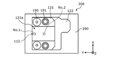
- the "top view” is when the mounting surface side is viewed from the normal direction of the mounting surface (main surface) of the base on which the light source is mounted. To say.
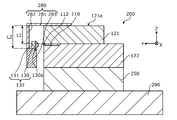
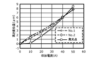
- the semiconductor laser element 110 By emitting the emitted light 300 to the semiconductor laser element 110, the semiconductor laser element 110 generates heat. Due to this heat generation, the upper base 121 undergoes thermal expansion and is displaced (changed) in the Z-axis direction.
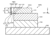
- the holding member 280 can hold the lens 130 from the gravity direction side applied to the lens 130 as compared with the case where the lens 130 is held on the upper surface or the side surface of the lens 130. Therefore, the lens 130 can be held more stably while maintaining the relative positional relationship between the semiconductor laser element 110 and the lens 130.
- the position and posture of the lens 130 can be adjusted to an appropriate state, and the position and posture of the lens 130 can be fixed.
Landscapes
- Physics & Mathematics (AREA)
- Condensed Matter Physics & Semiconductors (AREA)
- General Physics & Mathematics (AREA)
- Electromagnetism (AREA)
- Optics & Photonics (AREA)
- Semiconductor Lasers (AREA)
Priority Applications (4)
| Application Number | Priority Date | Filing Date | Title |
|---|---|---|---|
| US17/796,163 US20230110167A1 (en) | 2020-02-03 | 2021-01-22 | Semiconductor laser device |
| JP2021575727A JPWO2021157396A1 (https=) | 2020-02-03 | 2021-01-22 | |
| CN202180011715.5A CN115053417A (zh) | 2020-02-03 | 2021-01-22 | 半导体激光装置 |
| DE112021000855.2T DE112021000855T5 (de) | 2020-02-03 | 2021-01-22 | Halbleiter-Laservorrichtung |
Applications Claiming Priority (2)
| Application Number | Priority Date | Filing Date | Title |
|---|---|---|---|
| JP2020-016225 | 2020-02-03 | ||
| JP2020016225 | 2020-02-03 |
Publications (1)
| Publication Number | Publication Date |
|---|---|
| WO2021157396A1 true WO2021157396A1 (ja) | 2021-08-12 |
Family
ID=77200470
Family Applications (1)
| Application Number | Title | Priority Date | Filing Date |
|---|---|---|---|
| PCT/JP2021/002329 Ceased WO2021157396A1 (ja) | 2020-02-03 | 2021-01-22 | 半導体レーザ装置 |
Country Status (5)
| Country | Link |
|---|---|
| US (1) | US20230110167A1 (https=) |
| JP (1) | JPWO2021157396A1 (https=) |
| CN (1) | CN115053417A (https=) |
| DE (1) | DE112021000855T5 (https=) |
| WO (1) | WO2021157396A1 (https=) |
Families Citing this family (1)
| Publication number | Priority date | Publication date | Assignee | Title |
|---|---|---|---|---|
| JP7659183B2 (ja) * | 2021-06-25 | 2025-04-09 | 日亜化学工業株式会社 | レーザ光源 |
Citations (5)
| Publication number | Priority date | Publication date | Assignee | Title |
|---|---|---|---|---|
| US5420722A (en) * | 1993-10-25 | 1995-05-30 | Creo Products Inc. | Self-registering microlens for laser diodes |
| JPH09269439A (ja) * | 1996-03-29 | 1997-10-14 | Nec Corp | 半導体レーザモジュール |
| JP2004200634A (ja) * | 2002-12-13 | 2004-07-15 | Hentze-Lissotschenko Patentverwaltungs Gmbh & Co Kg | 半導体レーザ装置、および半導体レーザ装置のための半導体レーザモジュール、ならびに半導体レーザ装置を製造するための方法 |
| US20130084039A1 (en) * | 2011-08-16 | 2013-04-04 | International Business Machines Corporation | Lens array optical coupling to photonic chip |
| WO2019009086A1 (ja) * | 2017-07-07 | 2019-01-10 | パナソニックIpマネジメント株式会社 | 半導体レーザ装置 |
Family Cites Families (5)
| Publication number | Priority date | Publication date | Assignee | Title |
|---|---|---|---|---|
| DE68920011T2 (de) * | 1988-03-22 | 1995-06-01 | Fujitsu Ltd | Optische halbleiteranordung und deren herstellung. |
| US6078437A (en) * | 1998-09-28 | 2000-06-20 | Blue Sky Research | Micro-optic lens with integral alignment member |
| EP1006382B1 (de) | 1998-10-30 | 2002-09-18 | Lissotschenko, Vitalij | Anordnung und Vorrichtung zur optischen Strahltransformation |
| JP2002232064A (ja) * | 2001-02-05 | 2002-08-16 | Hamamatsu Photonics Kk | 半導体レーザ装置、及び、半導体レーザ装置のレンズ位置固定方法 |
| JP6964469B2 (ja) * | 2017-08-30 | 2021-11-10 | シャープ株式会社 | 光源装置およびその製造方法 |
-
2021
- 2021-01-22 US US17/796,163 patent/US20230110167A1/en not_active Abandoned
- 2021-01-22 WO PCT/JP2021/002329 patent/WO2021157396A1/ja not_active Ceased
- 2021-01-22 CN CN202180011715.5A patent/CN115053417A/zh active Pending
- 2021-01-22 DE DE112021000855.2T patent/DE112021000855T5/de active Pending
- 2021-01-22 JP JP2021575727A patent/JPWO2021157396A1/ja not_active Ceased
Patent Citations (5)
| Publication number | Priority date | Publication date | Assignee | Title |
|---|---|---|---|---|
| US5420722A (en) * | 1993-10-25 | 1995-05-30 | Creo Products Inc. | Self-registering microlens for laser diodes |
| JPH09269439A (ja) * | 1996-03-29 | 1997-10-14 | Nec Corp | 半導体レーザモジュール |
| JP2004200634A (ja) * | 2002-12-13 | 2004-07-15 | Hentze-Lissotschenko Patentverwaltungs Gmbh & Co Kg | 半導体レーザ装置、および半導体レーザ装置のための半導体レーザモジュール、ならびに半導体レーザ装置を製造するための方法 |
| US20130084039A1 (en) * | 2011-08-16 | 2013-04-04 | International Business Machines Corporation | Lens array optical coupling to photonic chip |
| WO2019009086A1 (ja) * | 2017-07-07 | 2019-01-10 | パナソニックIpマネジメント株式会社 | 半導体レーザ装置 |
Also Published As
| Publication number | Publication date |
|---|---|
| CN115053417A (zh) | 2022-09-13 |
| US20230110167A1 (en) | 2023-04-13 |
| DE112021000855T5 (de) | 2022-12-08 |
| JPWO2021157396A1 (https=) | 2021-08-12 |
Similar Documents
| Publication | Publication Date | Title |
|---|---|---|
| EP1830443A1 (en) | High Power Diode Laser Having Multiple Emitters and Method for its Production | |
| EP3605754A1 (en) | Optical module | |
| CN107005022A (zh) | 光学单元、光学单元的固定结构及半导体激光器模块 | |
| JP5764152B2 (ja) | 半導体レーザ装置 | |
| WO2021157396A1 (ja) | 半導体レーザ装置 | |
| CA2717476C (en) | Optical module | |
| JP2017208483A (ja) | 半導体レーザ装置 | |
| JP2020145355A (ja) | 半導体レーザ装置 | |
| JP2020145291A (ja) | 半導体レーザ装置の製造方法、及び、半導体レーザ装置 | |
| JP2024123275A (ja) | 発光装置 | |
| JP7431553B2 (ja) | 半導体レーザ装置 | |
| JP7515075B2 (ja) | レーザ装置およびレーザ装置の光軸調整方法 | |
| WO2022030223A1 (ja) | 半導体レーザ装置 | |
| JP2023161108A (ja) | レーザ光源およびその製造方法 | |
| JP7269140B2 (ja) | 半導体レーザ装置 | |
| US20260106431A1 (en) | Light emitting device and light emitting module | |
| JP7172445B2 (ja) | 光学ユニット及び光学装置 | |
| US20080049299A1 (en) | Packaging of frequency-doubled, extended-cavity, surface-emitting laser components on a common substrate | |
| JP7440492B2 (ja) | 半導体レーザ装置 | |
| JP6417885B2 (ja) | 光モジュール | |
| US20220285916A1 (en) | Semiconductor laser device | |
| US20190242548A1 (en) | Optical unit and optical apparatus | |
| WO2020065819A1 (ja) | レーザ光源装置 | |
| JP2004241438A (ja) | 光ビーム発生装置 | |
| EP4564617A1 (en) | Light-emitting module |
Legal Events
| Date | Code | Title | Description |
|---|---|---|---|
| 121 | Ep: the epo has been informed by wipo that ep was designated in this application |
Ref document number: 21750430 Country of ref document: EP Kind code of ref document: A1 |
|
| ENP | Entry into the national phase |
Ref document number: 2021575727 Country of ref document: JP Kind code of ref document: A |
|
| 122 | Ep: pct application non-entry in european phase |
Ref document number: 21750430 Country of ref document: EP Kind code of ref document: A1 |