WO2021153736A1 - 弾性波デバイスおよびそれを備えたラダー型フィルタ - Google Patents
弾性波デバイスおよびそれを備えたラダー型フィルタ Download PDFInfo
- Publication number
- WO2021153736A1 WO2021153736A1 PCT/JP2021/003252 JP2021003252W WO2021153736A1 WO 2021153736 A1 WO2021153736 A1 WO 2021153736A1 JP 2021003252 W JP2021003252 W JP 2021003252W WO 2021153736 A1 WO2021153736 A1 WO 2021153736A1
- Authority
- WO
- WIPO (PCT)
- Prior art keywords
- resonator
- reflector
- elastic wave
- electrode
- value
- Prior art date
Links
- 239000000758 substrate Substances 0.000 claims abstract description 28
- 230000000903 blocking effect Effects 0.000 claims description 40
- 239000000463 material Substances 0.000 claims description 12
- 239000011295 pitch Substances 0.000 description 67
- 238000010897 surface acoustic wave method Methods 0.000 description 30
- VYPSYNLAJGMNEJ-UHFFFAOYSA-N Silicium dioxide Chemical compound O=[Si]=O VYPSYNLAJGMNEJ-UHFFFAOYSA-N 0.000 description 12
- 230000007423 decrease Effects 0.000 description 11
- 238000012986 modification Methods 0.000 description 10
- 230000004048 modification Effects 0.000 description 10
- 229910052581 Si3N4 Inorganic materials 0.000 description 7
- 230000000052 comparative effect Effects 0.000 description 7
- HQVNEWCFYHHQES-UHFFFAOYSA-N silicon nitride Chemical compound N12[Si]34N5[Si]62N3[Si]51N64 HQVNEWCFYHHQES-UHFFFAOYSA-N 0.000 description 7
- 235000012239 silicon dioxide Nutrition 0.000 description 6
- 239000000377 silicon dioxide Substances 0.000 description 6
- 230000005540 biological transmission Effects 0.000 description 5
- 238000010586 diagram Methods 0.000 description 5
- 230000001902 propagating effect Effects 0.000 description 5
- OKTJSMMVPCPJKN-UHFFFAOYSA-N Carbon Chemical compound [C] OKTJSMMVPCPJKN-UHFFFAOYSA-N 0.000 description 4
- XUIMIQQOPSSXEZ-UHFFFAOYSA-N Silicon Chemical compound [Si] XUIMIQQOPSSXEZ-UHFFFAOYSA-N 0.000 description 4
- 229910052799 carbon Inorganic materials 0.000 description 4
- 239000011521 glass Substances 0.000 description 4
- 229910052710 silicon Inorganic materials 0.000 description 4
- 239000010703 silicon Substances 0.000 description 4
- WSMQKESQZFQMFW-UHFFFAOYSA-N 5-methyl-pyrazole-3-carboxylic acid Chemical compound CC1=CC(C(O)=O)=NN1 WSMQKESQZFQMFW-UHFFFAOYSA-N 0.000 description 3
- PNEYBMLMFCGWSK-UHFFFAOYSA-N aluminium oxide Inorganic materials [O-2].[O-2].[O-2].[Al+3].[Al+3] PNEYBMLMFCGWSK-UHFFFAOYSA-N 0.000 description 3
- PMHQVHHXPFUNSP-UHFFFAOYSA-M copper(1+);methylsulfanylmethane;bromide Chemical compound Br[Cu].CSC PMHQVHHXPFUNSP-UHFFFAOYSA-M 0.000 description 3
- 229910003460 diamond Inorganic materials 0.000 description 3
- 239000010432 diamond Substances 0.000 description 3
- -1 duty Substances 0.000 description 3
- BPUBBGLMJRNUCC-UHFFFAOYSA-N oxygen(2-);tantalum(5+) Chemical compound [O-2].[O-2].[O-2].[O-2].[O-2].[Ta+5].[Ta+5] BPUBBGLMJRNUCC-UHFFFAOYSA-N 0.000 description 3
- 230000000644 propagated effect Effects 0.000 description 3
- 230000001681 protective effect Effects 0.000 description 3
- HBMJWWWQQXIZIP-UHFFFAOYSA-N silicon carbide Chemical compound [Si+]#[C-] HBMJWWWQQXIZIP-UHFFFAOYSA-N 0.000 description 3
- 229910010271 silicon carbide Inorganic materials 0.000 description 3
- 229910001936 tantalum oxide Inorganic materials 0.000 description 3
- ZOXJGFHDIHLPTG-UHFFFAOYSA-N Boron Chemical compound [B] ZOXJGFHDIHLPTG-UHFFFAOYSA-N 0.000 description 2
- PXGOKWXKJXAPGV-UHFFFAOYSA-N Fluorine Chemical compound FF PXGOKWXKJXAPGV-UHFFFAOYSA-N 0.000 description 2
- 229910013641 LiNbO 3 Inorganic materials 0.000 description 2
- PXHVJJICTQNCMI-UHFFFAOYSA-N Nickel Chemical compound [Ni] PXHVJJICTQNCMI-UHFFFAOYSA-N 0.000 description 2
- 238000013459 approach Methods 0.000 description 2
- 229910052796 boron Inorganic materials 0.000 description 2
- 150000001875 compounds Chemical class 0.000 description 2
- 238000013016 damping Methods 0.000 description 2
- 230000006866 deterioration Effects 0.000 description 2
- 229910052731 fluorine Inorganic materials 0.000 description 2
- 239000011737 fluorine Substances 0.000 description 2
- TWNQGVIAIRXVLR-UHFFFAOYSA-N oxo(oxoalumanyloxy)alumane Chemical compound O=[Al]O[Al]=O TWNQGVIAIRXVLR-UHFFFAOYSA-N 0.000 description 2
- BASFCYQUMIYNBI-UHFFFAOYSA-N platinum Chemical compound [Pt] BASFCYQUMIYNBI-UHFFFAOYSA-N 0.000 description 2
- PIGFYZPCRLYGLF-UHFFFAOYSA-N Aluminum nitride Chemical compound [Al]#N PIGFYZPCRLYGLF-UHFFFAOYSA-N 0.000 description 1
- 101100219315 Arabidopsis thaliana CYP83A1 gene Proteins 0.000 description 1
- VYZAMTAEIAYCRO-UHFFFAOYSA-N Chromium Chemical compound [Cr] VYZAMTAEIAYCRO-UHFFFAOYSA-N 0.000 description 1
- RYGMFSIKBFXOCR-UHFFFAOYSA-N Copper Chemical compound [Cu] RYGMFSIKBFXOCR-UHFFFAOYSA-N 0.000 description 1
- 101000806846 Homo sapiens DNA-(apurinic or apyrimidinic site) endonuclease Proteins 0.000 description 1
- 101000835083 Homo sapiens Tissue factor pathway inhibitor 2 Proteins 0.000 description 1
- ZOKXTWBITQBERF-UHFFFAOYSA-N Molybdenum Chemical compound [Mo] ZOKXTWBITQBERF-UHFFFAOYSA-N 0.000 description 1
- 101100269674 Mus musculus Alyref2 gene Proteins 0.000 description 1
- 101100140580 Saccharomyces cerevisiae (strain ATCC 204508 / S288c) REF2 gene Proteins 0.000 description 1
- 229910004298 SiO 2 Inorganic materials 0.000 description 1
- BQCADISMDOOEFD-UHFFFAOYSA-N Silver Chemical compound [Ag] BQCADISMDOOEFD-UHFFFAOYSA-N 0.000 description 1
- 102100026134 Tissue factor pathway inhibitor 2 Human genes 0.000 description 1
- RTAQQCXQSZGOHL-UHFFFAOYSA-N Titanium Chemical compound [Ti] RTAQQCXQSZGOHL-UHFFFAOYSA-N 0.000 description 1
- 239000000956 alloy Substances 0.000 description 1
- 229910045601 alloy Inorganic materials 0.000 description 1
- 229910052782 aluminium Inorganic materials 0.000 description 1
- XAGFODPZIPBFFR-UHFFFAOYSA-N aluminium Chemical compound [Al] XAGFODPZIPBFFR-UHFFFAOYSA-N 0.000 description 1
- 229910052804 chromium Inorganic materials 0.000 description 1
- 239000011651 chromium Substances 0.000 description 1
- 238000004891 communication Methods 0.000 description 1
- 229910052802 copper Inorganic materials 0.000 description 1
- 239000010949 copper Substances 0.000 description 1
- 239000013078 crystal Substances 0.000 description 1
- 230000002542 deteriorative effect Effects 0.000 description 1
- 239000003989 dielectric material Substances 0.000 description 1
- 230000000694 effects Effects 0.000 description 1
- PCHJSUWPFVWCPO-UHFFFAOYSA-N gold Chemical compound [Au] PCHJSUWPFVWCPO-UHFFFAOYSA-N 0.000 description 1
- 229910052737 gold Inorganic materials 0.000 description 1
- 239000010931 gold Substances 0.000 description 1
- 239000002648 laminated material Substances 0.000 description 1
- GQYHUHYESMUTHG-UHFFFAOYSA-N lithium niobate Chemical compound [Li+].[O-][Nb](=O)=O GQYHUHYESMUTHG-UHFFFAOYSA-N 0.000 description 1
- 229910052751 metal Inorganic materials 0.000 description 1
- 239000002184 metal Substances 0.000 description 1
- 238000000034 method Methods 0.000 description 1
- 229910052750 molybdenum Inorganic materials 0.000 description 1
- 239000011733 molybdenum Substances 0.000 description 1
- 229910052759 nickel Inorganic materials 0.000 description 1
- 229910000484 niobium oxide Inorganic materials 0.000 description 1
- URLJKFSTXLNXLG-UHFFFAOYSA-N niobium(5+);oxygen(2-) Chemical compound [O-2].[O-2].[O-2].[O-2].[O-2].[Nb+5].[Nb+5] URLJKFSTXLNXLG-UHFFFAOYSA-N 0.000 description 1
- 229910052697 platinum Inorganic materials 0.000 description 1
- 239000004065 semiconductor Substances 0.000 description 1
- 229910052709 silver Inorganic materials 0.000 description 1
- 239000004332 silver Substances 0.000 description 1
- 229910052714 tellurium Inorganic materials 0.000 description 1
- PORWMNRCUJJQNO-UHFFFAOYSA-N tellurium atom Chemical compound [Te] PORWMNRCUJJQNO-UHFFFAOYSA-N 0.000 description 1
- 239000010936 titanium Substances 0.000 description 1
- 229910052719 titanium Inorganic materials 0.000 description 1
- WFKWXMTUELFFGS-UHFFFAOYSA-N tungsten Chemical compound [W] WFKWXMTUELFFGS-UHFFFAOYSA-N 0.000 description 1
- 229910052721 tungsten Inorganic materials 0.000 description 1
- 239000010937 tungsten Substances 0.000 description 1
Images


Classifications
-
- H—ELECTRICITY
- H03—ELECTRONIC CIRCUITRY
- H03H—IMPEDANCE NETWORKS, e.g. RESONANT CIRCUITS; RESONATORS
- H03H9/00—Networks comprising electromechanical or electro-acoustic devices; Electromechanical resonators
- H03H9/02—Details
- H03H9/02535—Details of surface acoustic wave devices
- H03H9/02818—Means for compensation or elimination of undesirable effects
- H03H9/02842—Means for compensation or elimination of undesirable effects of reflections
-
- H—ELECTRICITY
- H03—ELECTRONIC CIRCUITRY
- H03H—IMPEDANCE NETWORKS, e.g. RESONANT CIRCUITS; RESONATORS
- H03H9/00—Networks comprising electromechanical or electro-acoustic devices; Electromechanical resonators
- H03H9/46—Filters
- H03H9/54—Filters comprising resonators of piezo-electric or electrostrictive material
- H03H9/56—Monolithic crystal filters
- H03H9/566—Electric coupling means therefor
- H03H9/568—Electric coupling means therefor consisting of a ladder configuration
-
- H—ELECTRICITY
- H03—ELECTRONIC CIRCUITRY
- H03H—IMPEDANCE NETWORKS, e.g. RESONANT CIRCUITS; RESONATORS
- H03H9/00—Networks comprising electromechanical or electro-acoustic devices; Electromechanical resonators
- H03H9/02—Details
- H03H9/02535—Details of surface acoustic wave devices
- H03H9/02543—Characteristics of substrate, e.g. cutting angles
- H03H9/02574—Characteristics of substrate, e.g. cutting angles of combined substrates, multilayered substrates, piezoelectrical layers on not-piezoelectrical substrate
-
- H—ELECTRICITY
- H03—ELECTRONIC CIRCUITRY
- H03H—IMPEDANCE NETWORKS, e.g. RESONANT CIRCUITS; RESONATORS
- H03H9/00—Networks comprising electromechanical or electro-acoustic devices; Electromechanical resonators
- H03H9/02—Details
- H03H9/02535—Details of surface acoustic wave devices
- H03H9/02637—Details concerning reflective or coupling arrays
- H03H9/02685—Grating lines having particular arrangements
- H03H9/02771—Reflector banks
-
- H—ELECTRICITY
- H03—ELECTRONIC CIRCUITRY
- H03H—IMPEDANCE NETWORKS, e.g. RESONANT CIRCUITS; RESONATORS
- H03H9/00—Networks comprising electromechanical or electro-acoustic devices; Electromechanical resonators
- H03H9/02—Details
- H03H9/02535—Details of surface acoustic wave devices
- H03H9/02992—Details of bus bars, contact pads or other electrical connections for finger electrodes
-
- H—ELECTRICITY
- H03—ELECTRONIC CIRCUITRY
- H03H—IMPEDANCE NETWORKS, e.g. RESONANT CIRCUITS; RESONATORS
- H03H9/00—Networks comprising electromechanical or electro-acoustic devices; Electromechanical resonators
- H03H9/02—Details
- H03H9/125—Driving means, e.g. electrodes, coils
- H03H9/145—Driving means, e.g. electrodes, coils for networks using surface acoustic waves
- H03H9/14538—Formation
- H03H9/14541—Multilayer finger or busbar electrode
-
- H—ELECTRICITY
- H03—ELECTRONIC CIRCUITRY
- H03H—IMPEDANCE NETWORKS, e.g. RESONANT CIRCUITS; RESONATORS
- H03H9/00—Networks comprising electromechanical or electro-acoustic devices; Electromechanical resonators
- H03H9/02—Details
- H03H9/125—Driving means, e.g. electrodes, coils
- H03H9/145—Driving means, e.g. electrodes, coils for networks using surface acoustic waves
- H03H9/14544—Transducers of particular shape or position
- H03H9/14547—Fan shaped; Tilted; Shifted; Slanted; Tapered; Arched; Stepped finger transducers
-
- H—ELECTRICITY
- H03—ELECTRONIC CIRCUITRY
- H03H—IMPEDANCE NETWORKS, e.g. RESONANT CIRCUITS; RESONATORS
- H03H9/00—Networks comprising electromechanical or electro-acoustic devices; Electromechanical resonators
- H03H9/46—Filters
- H03H9/64—Filters using surface acoustic waves
- H03H9/6423—Means for obtaining a particular transfer characteristic
- H03H9/6433—Coupled resonator filters
- H03H9/6483—Ladder SAW filters
Definitions
- the present disclosure relates to an elastic wave device and a ladder type filter provided with the elastic wave device, and more specifically, to a technique for miniaturizing the elastic wave device.
- Patent Document 1 discloses a filter device composed of a plurality of surface acoustic wave (SAW) resonators.
- SAW surface acoustic wave
- a surface acoustic wave resonator (Interdigital Transducer: IDT) is formed in order to suppress leakage of a signal propagated in the surface acoustic wave resonator from the resonator. ) Reflectors are placed at both ends of the electrode.
- IDT Interdigital Transducer
- the filter device using the surface acoustic wave resonator as described above may be used, for example, in a mobile terminal represented by a mobile phone or a smartphone.
- a mobile terminal represented by a mobile phone or a smartphone.
- devices constituting the mobile terminal such as a filter device, are also required to be further miniaturized and reduced in height.
- Patent Document 2 Japanese Patent Application Laid-Open No. 2002-176335
- a configuration has been proposed to reduce the overall size.
- simply sharing the reflector will lower the frequency characteristics of the entire device, and it is possible that the desired characteristics cannot be achieved. There is sex.
- the present invention has been made to solve the above problems, and an object of the present invention is to realize miniaturization of an elastic wave device formed by a plurality of resonators while suppressing a decrease in frequency characteristics of the device. That is.
- the elastic wave device includes a substrate having a piezoelectric layer, first resonators and second resonators arranged on the substrate, and a shared reflector.
- the second resonator is arranged adjacent to the first resonator on the substrate, and has different frequency characteristics from the first resonator.
- the common reflector is arranged between the first resonator and the second resonator on the substrate, and functions as a reflector for both the first resonator and the second resonator.
- the first resonator includes a first IDT electrode in which the electrode fingers are formed at the first pitch.
- the second resonator includes a second IDT electrode in which the electrode fingers are formed at a second pitch.
- the lower limit frequency of the blocking region of the shared reflector is the same as the lower limit frequency of the blocking region of the first resonator and the lower limit frequency of the blocking region of the second resonator, or the lower limit frequency of the blocking region of the first resonator and the second. It is between the lower limit frequency of the resonator blocking region.
- the upper limit frequency of the blocking region of the shared reflector is the same as the upper limit frequency of the blocking region of the first resonator and the upper limit frequency of the blocking region of the second resonator, or the upper limit frequency of the blocking region of the first resonator and the second. It is between the upper limit frequency of the resonator blocking region.
- the elastic wave device includes a substrate having a piezoelectric layer, first resonators and second resonators arranged on the substrate, and a shared reflector.
- the second resonator is arranged adjacent to the first resonator on the substrate, and has different frequency characteristics from the first resonator.
- the common reflector is arranged between the first resonator and the second resonator on the substrate, and functions as a reflector for both the first resonator and the second resonator.
- the first resonator includes a first IDT electrode in which the electrode fingers are formed at the first pitch.
- the second resonator includes a second IDT electrode in which the electrode fingers are formed at a second pitch.
- the values obtained by multiplying the pitch of the electrode fingers, the duty of the electrode fingers, and the thickness of the electrode fingers are the first value, the second value, and the third value, respectively. If so, the first value is the same as the second and third values, or is between the second and third values.
- a shared reflector that functions as both reflectors is arranged between two elastic wave resonators (first resonator and second resonator), each containing an IDT electrode. Will be done. Then, the lower limit frequency of the blocking region in the shared reflector is set between the lower limit frequencies of the blocking region of the two resonators, and the upper limit frequency of the blocking region in the shared reflector is the upper limit of the blocking region of the two resonators. Set between frequencies. With such a configuration, the signal from the IDT of any resonator is reflected by the shared reflector. Therefore, it is possible to realize miniaturization while suppressing a decrease in the frequency characteristics of the elastic wave device.
- FIG. It is a top view of the elastic wave device of the comparative example. It is a top view of the filter apparatus including the elastic wave device in Embodiment 1 and the comparative example. It is a figure for demonstrating the detailed structure of the part of region RG1 of FIG. 5 (b). It is a figure for demonstrating the detailed structure of the part of region RG2 of FIG. 5 (b). It is a figure for demonstrating the frequency characteristic of the elastic wave device of the comparative example.
- FIG. It is a figure for demonstrating the frequency characteristic of the elastic wave device of Embodiment 1.
- FIG. It is a figure which shows an example of the specification of the elastic wave device which concerns on Embodiment 1.
- FIG. It is a top view of the elastic wave device which concerns on the modification 1.
- FIG. It is sectional drawing of the elastic wave device which concerns on Embodiment 2.
- FIG. It is a figure which shows an example of the specification of the elastic wave device which concerns on Embodiment 2.
- FIG. It is sectional drawing of the elastic wave device which concerns on Embodiment 3.
- FIG. It is a figure which shows an example of the specification of the elastic wave device which concerns on Embodiment 3.
- FIG. It is sectional drawing of the elastic wave device which concerns on Embodiment 4.
- FIG. It is a figure which shows another example of the arrangement of the dielectric layer.
- FIG. 1 is a diagram showing a circuit configuration of a filter device 10 formed by an elastic wave device according to the first embodiment.
- the filter device 10 is, for example, a filter device used in a transmission side circuit of a communication device, and is a ladder type filter connected between a transmission terminal TX and an antenna terminal ANT.
- the filter device 10 filters the signal received by the transmission terminal TX and outputs it from the antenna terminal ANT.
- the filter device 10 includes series arm resonance portions S1 to S5 connected in series between the transmission terminal TX and the antenna terminal ANT, and parallel arm resonance portions P1 to P4.
- Each resonance portion of the series arm resonance portions S1 to S5 and the parallel arm resonance portions P1 to P4 includes at least one elastic wave resonator.
- each resonance portion of the series arm resonance portions S1 and S5 and the parallel arm resonance portions P1 to P4 is composed of one elastic wave resonator, and each resonance portion of the series arm resonance portions S2 to S4 is 2. It is composed of two elastic wave resonators.
- the series arm resonance portion S2 includes elastic wave resonators S21 and S22 connected in series.
- the series arm resonance portion S3 includes elastic wave resonators S31 and S32 connected in series.
- the series arm resonance portion S4 includes elastic wave resonators S41 and S42 connected in series.
- the number of elastic wave resonators included in each resonance portion is not limited to this, and is appropriately selected according to the characteristics of the filter device.
- an elastic surface wave (SAW) resonator can be used as the surface acoustic wave resonator.
- One end of the parallel arm resonance portion P1 is connected to a connection point between the series arm resonance portion S1 and the series arm resonance portion S2, and the other end is connected to the ground potential.
- One end of the parallel arm resonance portion P2 is connected to a connection point between the series arm resonance portion S2 and the series arm resonance portion S3, and the other end is connected to the ground potential.
- One end of the parallel arm resonance portion P3 is connected to a connection point between the series arm resonance portion S3 and the series arm resonance portion S4, and the other end is connected to the ground potential.
- One end of the parallel arm resonance portion P4 is connected to a connection point between the series arm resonance portion S4 and the series arm resonance portion S5, and the other end is connected to the ground potential.
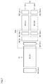
- FIG. 2 is a top view of a portion of the elastic wave device 100 in which a shared reflector is formed between adjacent resonators.
- FIG. 3 is a cross-sectional view of a portion between adjacent resonators.
- the elastic wave device 100 includes two adjacent elastic wave resonators 101 and 102 and a shared reflector REF12.
- the elastic wave resonators 101 and 102 included in the elastic wave device 100 are the resonators included in any of the series arm resonance portions S1 to S5 and the parallel arm resonance portions P1 to P4 in the filter device 10 described with reference to FIG. handle.
- Surface acoustic wave resonators 101 and 102 are SAW resonators including an IDT electrode.
- the elastic wave resonator 101 includes an IDT electrode IDT1 and reflectors REF1-1 and REF1-2 arranged at both ends of the IDT electrode IDT1.
- the elastic wave resonator 102 includes an IDT electrode IDT2 and reflectors REF2-1 and REF2-2 arranged at both ends of the IDT electrode IDT2.
- the IDT electrode surface acoustic waves propagate in the direction orthogonal to the extending direction of the opposing electrode fingers.
- the reflector is used to reflect the surface acoustic waves leaking from the end of the IDT electrode and confine it in the IDT electrode. Thereby, the Q value of the elastic wave resonator can be increased.
- the IDT electrode and the reflector formed by each elastic wave resonator are formed on the substrate 105 having the piezoelectric layer 110.
- the substrate 105 includes a low sound velocity layer 121, a high sound velocity layer 122, and a support layer 130.
- the support layer 130 is, for example, a semiconductor substrate made of silicon (Si).
- the hypersonic layer 122, the low sound velocity layer 121, and the piezoelectric layer 110 are laminated in this order on the support layer 130 in the positive direction of the Z axis of FIG.
- the piezoelectric layer 110 is formed of, for example, a piezoelectric single crystal material such as lithium tantalate (LiTaO 3 ) or lithium niobate (LiNbO 3 ), or a piezoelectric laminated material composed of aluminum nitride (AlN), LiTaO 3 or LiNbO 3. Will be done.
- An IDT electrode and a reflector, which are functional elements, are formed on the upper surface of the piezoelectric layer 110 (the surface in the positive direction of the Z axis).
- lithium tantalate (LT) is used as the piezoelectric layer 110.
- IDT electrodes and reflectors are made of, for example, a single metal consisting of at least one of aluminum, copper, silver, gold, titanium, tungsten, platinum, chromium, nickel and molybdenum, or a material such as an alloy containing these as main components. There is.
- the low-pitched sound layer 121 is made of a material in which the bulk wave sound velocity propagating through the low-pitched sound layer 121 is lower than the bulk wave sound velocity propagating through the piezoelectric layer 110.
- the low sound velocity layer 121 is made of silicon dioxide (SiO 2 ).
- the bass velocity layer 121 is not limited to silicon dioxide, and may be formed of, for example, other dielectrics such as glass, silicon oxynitride, and tantalum oxide, or a compound obtained by adding fluorine, carbon, boron, etc. to silicon dioxide. good.
- the hypersonic layer 122 is made of a material in which the bulk wave sound velocity propagating in the hypersonic layer 122 is higher than the elastic wave sound velocity propagating in the piezoelectric layer 110.
- the hypersonic layer 122 is made of silicon nitride (SiN).
- the treble speed layer 122 is not limited to silicon nitride, and may be formed of a material such as aluminum nitride, aluminum oxide (alumina), silicon oxynitride, silicon carbide, diamond-like carbon (DLC), and diamond.
- the low sound speed layer 121 and the high sound speed layer 122 function as a reflection layer (mirror layer) 120. That is, the surface acoustic wave leaking from the piezoelectric layer 110 toward the support layer 130 is reflected by the high sound velocity layer 122 due to the difference in the propagating sound velocity, and is confined in the low sound velocity layer 121. In this way, the loss of acoustic energy of the surface acoustic wave propagated by the reflective layer 120 is suppressed, so that the surface acoustic wave can be efficiently propagated.
- a reflection layer 120 mirror layer
- the reflection layer 120 includes a plurality of low sound speed layers 121 and high sound speed layers 122.
- the configuration may be arranged alternately.
- the reflector REF1-1 of the elastic wave resonator 101 is arranged at the end of the IDT electrode IDT1 on the elastic wave resonator 102 side.
- the reflector REF1-2 is arranged at an end opposite to the reflector REF1-1 with respect to the IDT electrode IDT1.
- the electrode fingers of the reflectors REF1-1 and REF1-2 are formed at the same pitch as the electrode fingers of the IDT electrode IDT1.
- the reflector REF2-1 of the elastic wave resonator 102 is arranged at the end of the IDT electrode IDT2 on the elastic wave resonator 101 side.
- the reflector REF2-2 is arranged at an end opposite to the reflector REF2-1 with respect to the IDT electrode IDT2.
- the electrode fingers of the reflectors REF2-1 and REF2-2 are formed at the same pitch as the electrode fingers of the IDT electrode IDT2.
- the shared reflector REF12 is arranged between the reflector REF1-1 of the elastic wave resonator 101 and the reflector REF2-1 of the elastic wave resonator 102.
- the sum of the number of electrode fingers of the reflector REF1-1 and the number of electrode fingers of the shared reflector REF12 is set to the same number as the number of electrode fingers of the reflector REF1-2.
- the sum of the number of electrode fingers of the reflector REF2-1 and the number of electrode fingers of the shared reflector REF12 is set to the same number as the number of electrode fingers of the reflector REF2-2.
- the length of the electrode finger of the common reflector REF12 is longer than the crossing width of the electrode finger in the IDT electrode included in the elastic wave resonator 101 and the elastic wave resonator 102.
- the frequency characteristic of the shared reflector REF12 has an intermediate frequency characteristic between the frequency characteristic of the elastic wave resonator 101 and the frequency characteristic of the elastic wave resonator 102. With such a configuration, the shared reflector REF12 functions as a reflector for both the elastic wave resonator 101 and the elastic wave resonator 102.
- At least a part of the electrode fingers of the shared reflector REF12 is the pitch of the electrode fingers of the IDT electrode IDT1 and the reflectors REF1-1 and REF1-2 in the elastic wave resonator 101 (first pitch: PT1). ) And the pitch between the IDT electrode IDT2 in the elastic wave resonator 102 and the pitch of the electrode fingers of the reflectors REF2-1 and REF2-2 (second pitch: PT2) to obtain intermediate frequency characteristics. It has been realized.
- the pitch of the electrode fingers is the distance between the centers of the adjacent electrode fingers.
- the frequency characteristics can be measured by bringing the contact pins connected to the network analyzer into contact with each resonator and the wiring connected to the reflector as little as possible.
- the entire electrode finger may be formed at an intermediate pitch, or the pitch is gradually changed from the elastic wave resonator 101 toward the elastic wave resonator 102. There may be. Further, the pitch may be changed stepwise from the elastic wave resonator 101 toward the elastic wave resonator 102.
- the reflector REF1-1 in the elastic wave resonator 101 and the reflector REF2-1 in the elastic wave resonator 102 are not always indispensable, and the IDT electrode IDT1 of the elastic wave resonator 101 and the IDT electrode IDT2 of the elastic wave resonator 102
- the configuration may be such that only the shared reflector REF12 is arranged between the two.
- the number of electrode fingers of the shared reflector REF12 is preferably the same as the number of electrode fingers of the reflector REF1-2 and the reflector REF2-2.
- FIG. 4 is a top view of an adjacent resonator in the elastic wave device 100 # of the comparative example.
- the elastic wave device 100 # includes two adjacent elastic wave resonators 101 # and 102 #.
- reflectors (REF1-2, REF2-2) having the same shape are arranged at both ends of the IDT electrodes of each elastic wave resonator. That is, in each elastic wave resonator, the number of electrode fingers of the reflectors arranged at both ends is the same. Therefore, for example, when the number of electrode fingers of each reflector REF1-2 and REF2-2 is 20, the total number of electrode fingers of the reflector arranged between the two IDT electrodes is 40.
- the number of electrode fingers of each reflector REF1-1 and REF2-1 is eight, and the number of electrode fingers of the shared reflector REF12 is twelve.
- the total number of electrode fingers of the reflector REF1-1 and the shared reflector REF12, and the total number of electrode fingers of the reflector REF2-1 and the shared reflector REF12 are 20, respectively, and the reflectors REF1-2 and REF2-2 The number is the same as the number of electrode fingers.
- the total number of electrode fingers of the reflector arranged between the two IDT electrodes is as small as 28.
- the distance between the two IDT electrodes can be narrowed while maintaining the number of electrode fingers that function as reflectors for each elastic wave resonator and suppressing the decrease in reflectance.
- the elastic wave device 100 can be miniaturized as compared with the elastic wave device 100 # of the comparative example.
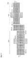
- FIG. 5 is a plan view of a filter device including an elastic wave device according to a comparative example and the first embodiment.
- FIG. 5A shows a case where the configuration of the elastic wave device of the comparative example is included
- FIG. 5B shows a case where the configuration of the elastic wave device of the first embodiment is included.
- the portion between the series arm resonance portion S2 (elastic wave resonators S21, S22) and the parallel arm resonance portion P1 (region RG1 in FIG. 5B), and the series arm resonance portion S4 (elastic wave resonance).
- the configuration of the first embodiment is applied to the portion (region RG2 in FIG. 5B) between the child S41, S42) and the parallel arm resonance portion P4.
- the width W1 of the filter device 10 # is limited by the length of the portion where the elastic wave resonators are arranged adjacent to each other. Therefore, as in the filter device 10 of FIG. 5B, by arranging elastic wave resonators adjacent to each other in the regions RG1 and RG2 using a shared reflector, the width W2 of the filter device 10 can be compared. It can be made narrower than in the case of (W2 ⁇ W1).
- FIGS. 6 and 7 are diagrams for explaining the detailed configuration of the regions RG1 and RG2 in FIG. 5B, respectively.
- a reflector is shared between a parallel arm resonator composed of one elastic wave resonator and a series arm resonator composed of two elastic wave resonators. It has a structure of
- the elastic wave resonator S21 is configured to include an IDT electrode IDT_S21 and reflectors REF_S21-1 and REF_S21-2
- the elastic wave resonator S22 includes an IDT electrode IDT_S22 and a reflector. It is configured to include REF_S22-1 and REF_S22-2.
- the elastic wave resonator constituting the parallel arm resonance portion P1 includes an IDT electrode IDT_P1 and reflectors REF_P1-1 and REF_P1-2.
- the shared reflector REF_A is arranged so as to face the reflectors REF_S21-1, REF_S22-1, and REF_P1-1.
- the reflectors REF_S21-1 and REF_S22-1 are arranged adjacent to each other on the first end side of the shared reflector REF_A, and the reflector REF_P1-1 is arranged on the second end side of the shared reflector REF_A. ing.
- the length of the electrode finger of the common reflector REF_A is longer than the length of the electrode finger of the reflector REF_P1-1, and the length of the electrode finger of the reflector REF_S21-1 and the length of the electrode finger of the reflector REF_S22-1. It is set to be longer than the sum of.
- the distance from the end of the reflectors REF_S21-2 and REF_S22-2 to the end of the reflector REF_P1-2 is as compared with the case where the reflectors are individually arranged for each elastic wave resonator.
- the length can be shortened.
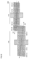
- the elastic wave resonator S41 includes an IDT electrode IDT_S41 and reflectors REF_S41-1 and REF_S41-2
- the elastic wave resonator S42 includes an IDT electrode IDT_S42 and a reflector. It is configured to include REF_S42-1 and REF_S42-2.
- the elastic wave resonator constituting the parallel arm resonance portion P4 includes an IDT electrode IDT_P4 and reflectors REF_P4-1 and REF_P4A-2.
- the shared reflector REF_B is arranged so as to face the reflectors REF_S41-1, REF_S42-1, and REF_P4-1.
- the reflectors REF_S41-1 and REF_S42-1 are arranged adjacent to each other on the first end side of the shared reflector REF_B, and the reflector REF_P4-1 is arranged on the second end side of the shared reflector REF_B. ing.
- the length of the electrode finger of the common reflector REF_B is longer than the length of the electrode finger of the reflector REF_P4-1, and the length of the electrode finger of the reflector REF_S41-1 and the length of the electrode finger of the reflector REF_S42-1. It is set to be longer than the sum of.
- the distance from the ends of the reflectors REF_S41-2 and REF_S42-2 to the ends of the reflectors REF_P4-2 The length can be shortened.
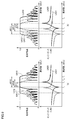
- FIGS. 8 and 9 the frequency characteristic of the reflectance coefficient of the reflector is shown in the upper row, and the frequency characteristic of the impedance of the resonator is shown in the lower row.
- the solid line LN10 and the solid line LN20 indicate the series arm resonator, and the broken line LN11 and the broken line LN21 indicate the parallel arm resonator.
- the ladder type filter as shown in FIG. 1 it is generally designed so that the resonance frequency of the series arm resonator and the antiresonance frequency of the parallel arm resonator substantially match. .. That is, in the reflector of the series arm resonator, the blocking region in which the reflectance coefficient gradually approaches 1 is between frequencies f2 and f4 (region AR10). On the other hand, in the reflector of the parallel arm resonator, the blocking region where the reflectance coefficient gradually approaches 1 is between frequencies f1 and f3 (region AR11).
- the reflectance coefficient of the shared reflector is, for example, It becomes like the one-dot chain line LN12 in FIG.
- the blocking region for the series arm resonator is expanded to the range of frequencies f2 to f31 (region AR16).
- the blocking region for the parallel arm resonator is extended to the frequency range f11 to f3 (region AR17), as shown in FIG. 9B.
- the lower limit frequency of the blocking region of the shared reflector is between the lower limit frequency of the blocking region of the first resonator and the lower limit frequency of the blocking region of the second resonator
- the upper limit frequency of the blocking region of the shared reflector is , It is between the upper limit frequency of the blocking region of the first resonator and the upper limit frequency of the blocking region of the second resonator. Therefore, as compared with the case where the electrode finger pitch of the shared reflector is unified to the electrode finger pitch of either resonator, the blocking range in the filter device can be expanded, and as a result, deterioration of the filter characteristics can be suppressed. Can be done.
- the "blocking region” indicates a frequency range having a reflection coefficient higher than 70% of the peak value of the reflection coefficient.
- the lower limit frequency of the blocking region corresponds to the resonance frequency of each resonator.
- the upper limit frequency of the blocking region corresponds to the frequency at which the stopband ripple (regions RG10 and RG11 in FIG. 8) begins to appear in the impedance characteristics of each resonator.
- the intensity of the surface acoustic wave excited is maximum in the central region of the IDT electrode, and decreases monotonically in the region of the reflectors at both ends as the distance from the central region increases. Therefore, the farther the common reflector is from the IDT electrode, the smaller the effect of the decrease in reflectance even if the electrode finger pitch is different from the electrode finger pitch of the IDT electrode. Therefore, by setting the electrode finger pitch in the shared reflector from the electrode finger pitch of one resonator to the electrode finger pitch of the other resonator gradually or stepwise, the frequencies f1 to 9 in FIG. 9 are set. It is possible to secure the reflectance between f11 and the frequencies f31 to f4, and the influence of the decrease in reflectance can be further reduced.
- the series arm resonator and the parallel arm resonator are adjacent to each other by using a shared reflector as shown in FIG. 9, the high frequency side and low frequency side ranges of the blocking region are not a little narrowed. Therefore, in the ladder type filter, in order to maintain the steepness of the attenuation characteristic at the end of the passband as the entire filter, a resonator forming the attenuation pole on the highest frequency side and an attenuation pole on the lowest frequency side are formed. It is preferable not to use a shared reflector for the resonator.
- the damping pole on the high frequency side is formed by the series arm resonator
- the damping pole on the low frequency side is formed by the parallel arm resonator. Therefore, in the series arm resonator including a plurality of series arm resonators, the series arm resonator (third) in which the electrode finger pitch is set narrower than that of the series arm resonator (first resonator) using the shared reflector. It is preferable to include a resonator).
- the parallel arm resonator including a plurality of parallel arm resonators
- the shared reflector is arranged between the two adjacent and the elastic wave resonator (first resonator, second resonator), and at least a part of the electrode finger pitch of the shared reflector is set to the second.
- the pitch between the electrode finger pitch of the IDT electrode of the 1 resonator and the electrode finger pitch of the IDT electrode of the second resonator is lowered. It is possible to realize the miniaturization of the elastic wave device while suppressing the above.
- FIG. 10 is a diagram showing an example of specifications of the elastic wave device 100 according to the first embodiment.
- the IDT electrode pair of the resonator 1 is 130 pairs, and the number of electrode fingers is 261.
- the number of pairs of IDT electrodes of the resonator 2 is 90 pairs, and the number of pairs is 181.
- the wavelength is 1.60700 ⁇ m, and the resonance frequency is 2358.11 MHz.
- the number of IDTs of the common reflector is eight, and the number of IDTs of the reflectors arranged between the common reflector and each IDT electrode is ten.
- the duty of each resonator is 0.5. Further, the film thicknesses of the electrode fingers of the resonator 1 and the resonator 2 are the same.
- the wavelength of the shared reflector gradually increases from 1.5495 ⁇ m to 1.90700 ⁇ m from the resonator 1 toward the resonator 2.
- the wavelength of the shared reflector electrode finger pitch
- the resonator 1 and the resonator 2 have the same film thickness and duty of the electrode fingers, the frequency of the resonator 2 having a large electrode finger pitch is lower than the frequency of the resonator 1.
- FIG. 11 is a top view of the elastic wave device 100A according to the first modification.
- the elastic wave device 100A includes elastic wave resonators 101A and 102A having the same configuration as in FIG. 2, and a shared reflector REF12A arranged between elastic wave resonators 101A and 102A.
- the elastic wave resonator 101A includes an IDT electrode IDT1A and reflectors REF1A-1 and REF1A-2.
- the elastic wave resonator 102A includes an IDT electrode IDT2A and reflectors REF2A-1 and REF2A-2.
- the elastic wave device 100A has a configuration in which the centers of the two elastic wave resonators 101A and 102A in the propagation direction of the elastic surface waves are offset and do not overlap. Specifically, it passes through the center of the crossing width of the electrode finger of the elastic wave resonator 101A, passes through the center of the crossing width of the virtual line CL1 orthogonal to the electrode finger, and the electrode finger of the elastic wave resonator 102A, and passes through the electrode.
- the virtual line CL2 orthogonal to the finger is offset in the extending direction of the electrode finger.
- the electrode finger of the shared reflector REF12A has a length facing both the electrode finger of the reflector REF1A-1 in the elastic wave resonator 101A and the electrode finger of the reflector REF2A-1 in the elastic wave resonator 102A. ing.
- the configuration is also applied to the regions RG1 and RG2 of the filter device 10 described in FIGS. 6 and 7.
- FIG. 12 is a top view of the elastic wave device 100B according to the second modification.
- the elastic wave device 100B includes elastic wave resonators 101B and 102B and shared reflectors REF12B arranged between elastic wave resonators 101B and 102B. Similar to the first modification, the elastic wave resonator 101B and the elastic wave resonator 102B are arranged at offset positions.
- the elastic wave resonator 101B includes an IDT electrode IDT1B and reflectors REF1B-1 and REF1B-2 arranged at both ends of the IDT electrode IDT1B.
- the elastic wave resonator 102B includes an IDT electrode IDT2B and reflectors REF2B-1 and REF2B-2 arranged at both ends of the IDT electrode IDT2B.
- the shared reflector REF12B is arranged between the reflector REF1B-1 and the reflector REF2B-1.
- the sum of the number of electrode fingers of the reflector REF1B-1 and the number of electrode fingers of the shared reflector REF12B is the same as the number of electrode fingers of the reflector REF1B-2.
- the sum of the number of electrode fingers of the reflector REF2B-1 and the number of electrode fingers of the shared reflector REF12B is the same as the number of electrode fingers of the reflector REF2B-2.
- the electrode fingers of the elastic wave resonators 101B and 102B and the common reflector REF12B are obliquely connected to the bus bar.
- the angle between the electrode finger and the bus bar is greater than 0 ° and less than 90 °.
- an elastic surface wave In a surface acoustic wave resonator, an elastic surface wave generally propagates in a direction orthogonal to the electrode finger. That is, as shown in FIG. 12, in the elastic wave resonator 101B, the elastic surface wave propagates in the direction of arrow RA1, and in the elastic wave resonator 102B, the elastic surface wave propagates in the direction of arrow RA2.
- the propagation direction of the elastic surface wave in one elastic wave resonator can be changed to the other elastic wave resonator. It can be outside the cross-width region of the electrode fingers in the IDT electrode of. Therefore, when the surface acoustic wave leaks from the common reflector, the influence on the other surface acoustic wave resonator can be further reduced.
- the duty of the electrode fingers of the shared reflector is set to an intermediate duty, so that the frequency characteristics of the shared reflector can be improved.
- the configuration to be adjusted will be described.
- the duty of the electrode finger is the ratio of the electrode finger to the pitch of the electrode finger (width of the electrode finger).
- FIG. 13 is a cross-sectional view of the elastic wave device 100C according to the second embodiment.
- the elastic wave device 100C includes an elastic wave resonators 101C and 102C and a shared reflector REF12C arranged between the elastic wave resonators 101C and 102C.
- the shared reflector REF12C includes a reflector REF1C-1 arranged at one end of the IDT electrode IDT1C of the elastic wave resonator 101C and a reflector REF2C-1 arranged at one end of the IDT electrode IDT2C of the elastic wave resonator 102C. It is placed between and. In the elastic wave device 100C, the electrode finger pitch of the elastic wave resonator 101C and the electrode finger pitch of the elastic wave resonator 102C are the same pitch.
- the duty (first duty) of the IDT electrode and the electrode finger of the reflector in the elastic wave resonator 101C is set to DT1
- the duty (second duty) of the electrode finger of the IDT electrode and the reflector in the elastic wave resonator 102C. Is set to DT2 (DT2> DT1).
- at least a part of the electrode fingers in the shared reflector REF12C is formed with an intermediate duty between the first duty DT1 and the second duty DT2 described above.
- the duty of the electrode finger of the shared reflector REF12C is set so as to gradually or gradually increase from the elastic wave resonator 101C toward the elastic wave resonator 102C.
- the frequency characteristic of the shared reflector is set to 2 by setting the duty to an intermediate duty for at least a part of the electrode fingers of the shared reflector. It can be set to a frequency characteristic between the frequency characteristics of one elastic wave resonator. As a result, it is possible to realize miniaturization of the elastic wave device while suppressing a decrease in the frequency characteristics of the elastic wave device as in the first embodiment.
- both the pitch and duty of the electrode fingers in the shared reflector may be set to intermediate values.
- FIG. 14 is a diagram showing an example of specifications of the elastic wave device 100C according to the second embodiment.
- the logarithm of each IDT electrode of the resonator 1 and the resonator 2 is 130 pairs, and the number of electrode fingers is 261.
- the number of IDTs of the common reflector is eight, and the number of IDTs of the reflectors arranged between the common reflector and each IDT electrode is ten.
- the resonance frequency of the resonator 1 is 2453.39 MHz, and the resonance frequency of the resonator 2 is 2446.86 MHz.
- the film thicknesses of the electrode fingers of the resonator 1 and the resonator 2 are the same.
- the duty of the resonator 1 is set to 0.5
- the duty of the resonator 2 is set to 0.55.
- the duty in the common reflector gradually changes from 0.5 to 0.55 from the resonator 1 toward the resonator 2.
- the duty of the shared reflector is set to an intermediate duty between the duties of the two resonators, it is possible to realize miniaturization of the elastic wave device while suppressing a decrease in the frequency characteristics of the elastic wave device. Can be done. Since the resonator 1 and the resonator 2 have the same electrode finger pitch and electrode finger film thickness, the frequency of the resonator 2 having a large duty is lower than the frequency of the resonator 1.
- FIG. 15 is a cross-sectional view of the elastic wave device 100D according to the third embodiment.
- the elastic wave device 100D includes an elastic wave resonators 101D and 102D and a shared reflector REF12D arranged between the elastic wave resonators 101D and 102D.
- the shared reflector REF12D includes a reflector REF1D-1 arranged at one end of the IDT electrode IDT1D of the elastic wave resonator 101D and a reflector REF2D-1 arranged at one end of the IDT electrode IDT2D of the elastic wave resonator 102D. It is placed between and.
- the pitch and duty of the electrode fingers of the elastic wave resonator 101D are the same as the pitch and duty of the electrode fingers of the elastic wave resonator 102D, but the electrodes of the two elastic wave resonators 101D and 102D.
- the film thickness of the fingers is different. Specifically, the film thickness of the electrode finger of the elastic wave resonator 101D (first electrode finger film thickness) is set to ET1, and the film thickness of the electrode finger of the elastic wave resonator 102D (second electrode finger film thickness). ) Is set to ET2 (ET2> ET1).
- the film thickness of at least a part of the electrode fingers in the shared reflector REF12D is formed to be an intermediate film thickness between the first electrode finger film thickness ET1 and the second electrode finger film thickness ET2.
- the film thickness of at least a part of the electrode fingers in the shared reflector REF12D is thicker than the first electrode finger film thickness ET1 and thinner than the second electrode finger film thickness ET2.
- the film thickness of the electrode finger of the shared reflector REF12D is set so as to gradually or gradually increase from the elastic wave resonator 101D toward the elastic wave resonator 102D.
- the frequency characteristics of the shared reflector can be set by setting the film thickness to an intermediate level for at least a part of the electrode fingers of the shared reflector. Can be set to a frequency characteristic between the frequency characteristics of two elastic wave resonators. As a result, it is possible to realize miniaturization of the elastic wave device while suppressing a decrease in the frequency characteristics of the elastic wave device as in the first embodiment.
- the pitch and / or duty of the electrode fingers of the common reflector is also intermediate. It may be set to a value.
- FIG. 16 is a diagram showing an example of specifications of the elastic wave device 100D according to the third embodiment.
- the IDT electrode pair of the resonator 1 is 130 pairs, and the number of electrode fingers is 261.
- the number of pairs of IDT electrodes of the resonator 2 is 90 pairs, and the number of electrode fingers is 181.
- the number of IDTs of the common reflector is eight, and the number of IDTs of the reflectors arranged between the common reflector and each IDT electrode is ten.
- the resonance frequency of the resonator 1 is 2453.39 MHz, and the resonance frequency of the resonator 2 is 2442.24 MHz.
- the duty of the IDT electrode is 0.5.
- the film thickness of the electrode finger in the resonator 1 is set to 121 nm
- the film thickness of the electrode finger in the resonator 2 is set to 131 nm.
- the thickness gradually increases from 121 nm to 131 nm from the resonator 1 toward the resonator 2.
- a dielectric layer may be placed on the IDT electrodes and reflectors to protect the functional elements on the substrate.
- the frequency characteristics of the elastic wave resonator also change depending on the thickness of the protective dielectric layer.
- the film thickness of the dielectric layer is set to an intermediate film thickness, which is shared. A configuration for adjusting the frequency characteristics of the reflector will be described.
- FIG. 17 is a cross-sectional view of the elastic wave device 100E according to the fourth embodiment.
- the elastic wave device 100E is arranged on the elastic wave resonators 101E and 102E, the shared reflectors REF12E arranged between the elastic wave resonators 101E and 102E, and the elastic wave resonators 101E and 102E and the shared reflectors REF12E. Includes a dielectric layer 140.
- the shared reflector REF12E includes a reflector REF1E-1 arranged at one end of the IDT electrode IDT1E of the elastic wave resonator 101E and a reflector REF2E-1 arranged at one end of the IDT electrode IDT2E of the elastic wave resonator 102E. It is placed between and.
- the pitch, duty, and film thickness of the IDT electrodes and reflectors of the elastic wave resonators 101E and 102E and the electrode fingers in the shared reflector REF12E are set to the same values.
- the dielectric layer 140 is made of a material such as silicon dioxide, glass, silicon nitride, tantalum oxide, silicon nitride, aluminum nitride, aluminum oxide (alumina), silicon nitride, silicon carbide, diamond-like carbon (DLC), and diamond. Yes, it may be formed of a compound in which fluorine, carbon, boron or the like is added to silicon dioxide.
- the dielectric layer 140 is arranged so as to cover the functional elements (IDT electrodes, reflectors) arranged on the piezoelectric layer 110 of the substrate 105.
- the film thickness (first dielectric film thickness) of the dielectric layer 140 arranged in the region of the elastic wave resonator 101E is set to FT1, and the dielectric layer arranged in the region of the elastic wave resonator 102E.
- the film thickness of 140 (second dielectric film thickness) is set to FT2 (FT1 ⁇ FT2).
- the dielectric layer 140 is made of a material having a bulk wave sound velocity slower than the resonance frequency of the elastic wave resonator (silicon dioxide, glass, tantalum oxide, niobium oxide, tellurium oxide, etc.), it is placed on the electrode finger.
- the thicker the arranged dielectric layer the larger the mass when the electrode finger vibrates, and therefore the lower the resonance frequency of the resonator. Therefore, in the configuration of FIG. 17, the resonance frequency of the elastic wave resonator 102E is lower than the resonance frequency of the elastic wave resonator 101E.
- the dielectric layer 140 is formed of a material having a bulk wave sound velocity faster than the resonance frequency of the elastic resonator (glass, silicon nitride, aluminum nitride, alumina, silicon oxynitride, silicon carbide, DLC, diamond, etc.).
- the thicker the dielectric layer the higher the resonance frequency of the resonator.
- the film thicknesses FT1 and FT2 of the dielectric layer 140 are defined as the distance from the upper surface of the electrode finger of the IDT electrode and the reflector to the surface of the dielectric layer 140. Further, in the dielectric layer 140, as shown in FIG. 18, the position of the upper surface of the dielectric in the portion with the electrode finger and the position of the upper surface of the dielectric in the portion without the electrode finger may be different.
- the film thickness of at least a part of the dielectric layer 140 arranged in the region of the shared reflector REF12E is an intermediate film thickness between the first dielectric film thickness FT1 and the second dielectric film thickness FT2. Is formed of.
- the film thickness of at least a part of the dielectric layer 140 arranged in the region of the common reflector REF12E is thinner than the first dielectric film thickness FT1 and thicker than the second dielectric film thickness FT2.
- the film thickness of the dielectric layer 140 arranged in the region of the shared reflector REF12E is set so as to gradually or gradually decrease from the elastic wave resonator 101E toward the elastic wave resonator 102E. ..
- the thickness of the protective dielectric layer arranged in the region of the adjacent elastic wave resonator is different, at least a part of the dielectric layer arranged in the region of the common reflector is intermediate.
- the frequency characteristic of the shared reflector can be set to the frequency characteristic between the frequency characteristics of the two elastic wave resonators. As a result, it is possible to realize miniaturization of the elastic wave device while suppressing a decrease in the frequency characteristics of the elastic wave device as in the first embodiment.
- the pitch, duty and / or film thickness of the electrode fingers of the two elastic wave resonators are different in addition to the film thickness of the dielectric layer, the pitch, duty and / or of the electrode fingers of the common reflector
- the film thickness may also be set to an intermediate value.
- the resonance frequency of the resonator, the frequency of the blocking region (upper limit frequency, lower limit frequency), and the frequency of the reflector (upper limit frequency, lower limit frequency) are the pitch of the electrode finger, the duty of the electrode finger, and the thickness of the electrode finger.
- the thickness of the piezoelectric layer, and the thickness of the dielectric layer show the same dependence tendency. As described above, the larger the respective parameters of the electrode finger pitch, the electrode finger duty, and the electrode finger thickness, the lower the resonance frequency of each resonator tends to be.
- the fourth value of the shared reflector REF12 is the fifth value and the elasticity of the elastic wave resonator 101. It is set so as to be between the sixth value of the wave resonator 102.
- the 7th value of the shared reflector REF12 is the 8th value of the elastic wave resonator 101. Is set to be between the 9th value of the elastic wave resonator 102 and the 9th value of the elastic wave resonator 102.
Abstract
Description
(フィルタ装置の構成)
図1は、実施の形態1に従う弾性波デバイスにより形成されるフィルタ装置10の回路構成を示す図である。フィルタ装置10は、たとえば、通信装置の送信側回路に用いられるフィルタ装置であり、送信用端子TXとアンテナ端子ANTとの間に接続されたラダー型フィルタである。フィルタ装置10は、送信用端子TXで受けた信号をフィルタリングしてアンテナ端子ANTから出力する。
次に、図2および図3を用いて、本実施の形態1に係る弾性波デバイス100の基本構成について説明する。図2は、弾性波デバイス100において、隣接共振子間に共用反射器が形成される部分の上面図である。また、図3は、隣接共振子間の部分の断面図である。
図2で示した実施の形態1の弾性波デバイス100においては、隣接して配置される2つの弾性波共振子が、弾性表面波の伝播方向の中心が一致するように、すなわちIDT電極の交叉幅の中心を通り電極指に直交する方向が一致するように配置されている構成について説明した。しかしながら、2つの弾性波共振子において弾性表面波の伝播方向の中心は異なっていてもよい。
実施の形態1および変形例1の弾性波デバイスにおいては、IDT電極および反射器における電極指が、電極指に接続されたバスバーに対して直交する方向に延在する構成について説明した。変形例2の弾性波デバイスにおいては、IDT電極および反射器の電極指が、バスバーに対して傾斜配置された構成について説明する。
実施の形態1においては、隣接する弾性波共振子の電極指ピッチが異なる構成の場合に、共用反射器の電極指のピッチを中間的なピッチにすることによって、共用反射器の周波数特性を調整する構成について説明した。
実施の形態3においては、隣接する弾性波共振子の電極指の膜厚が異なる構成の場合に、共用反射器の電極指の膜厚を中間的な膜厚とすることによって、共用反射器の周波数特性を調整する構成について説明する。
弾性波デバイスにおいては、基板上の機能素子を保護するために、IDT電極および反射器上に誘電体層が配置される場合がある。弾性波共振子の周波数特性は、この保護用の誘電体層の厚みによっても変化する。
Claims (20)
- 圧電層を有する基板と、
前記基板上に配置された第1共振子と、
前記基板上において前記第1共振子に隣接して配置され、前記第1共振子と周波数特性が異なる第2共振子と、
前記基板上において前記第1共振子と前記第2共振子との間に配置され、前記第1共振子および前記第2共振子の双方の反射器として機能する共用反射器とを備え、
前記第1共振子は、電極指が第1ピッチで形成された第1IDT(Interdigital Transducer)電極を含み、
前記第2共振子は、電極指が第2ピッチで形成された第2IDT電極を含み、
前記共用反射器の阻止域の下限周波数は、前記第1共振子の阻止域の下限周波数と前記第2共振子の阻止域の下限周波数と同じ、もしくは、前記第1共振子の阻止域の下限周波数と前記第2共振子の阻止域の下限周波数との間にあり、
前記共用反射器の阻止域の上限周波数は、前記第1共振子の阻止域の上限周波数と前記第2共振子の阻止域の上限周波数と同じ、もしくは、前記第1共振子の阻止域の上限周波数と前記第2共振子の阻止域の上限周波数との間にある、弾性波デバイス。 - 前記第2ピッチは、前記第1ピッチよりも狭く、
前記共用反射器の電極指の少なくとも一部は、前記第1ピッチおよび前記第2ピッチの間のピッチで形成される、請求項1に記載の弾性波デバイス。 - 前記共用反射器の電極指のピッチは、前記第1共振子から前記第2共振子に向かって徐々に狭くなる、請求項2に記載の弾性波デバイス。
- 前記共用反射器の電極指のピッチは、前記第1共振子から前記第2共振子に向かって段階的に狭くなる、請求項2に記載の弾性波デバイス。
- 前記第1共振子における電極指のデューティは第1デューティであり、前記第2共振子における電極指のデューティは前記第1デューティよりも大きい第2デューティであり、
前記共用反射器の電極指の少なくとも一部は、前記第1デューティおよび前記第2デューティの間のデューティで形成される、請求項1に記載の弾性波デバイス。 - 前記共用反射器の電極指のデューティは、前記第1共振子から前記第2共振子に向かって徐々に大きくなる、請求項5に記載の弾性波デバイス。
- 前記共用反射器の電極指のデューティは、前記第1共振子から前記第2共振子に向かって段階的に大きくなる、請求項5に記載の弾性波デバイス。
- 前記第1共振子の電極指の厚みは、前記第2共振子の電極指の厚みよりも薄く、
前記共用反射器の少なくとも一部の電極指の厚みは、前記第1共振子の電極指の厚みよりも厚く、かつ、前記第2共振子の電極指の厚みよりも薄い、請求項1に記載の弾性波デバイス。 - 前記第1共振子、前記第2共振子、および前記共用反射器の上に配置された誘電体層をさらに備え、
前記第1共振子の領域に配置された前記誘電体層の厚みは、前記第2共振子の領域に配置された前記誘電体層の厚みよりも厚く、
前記共用反射器の領域に配置された前記誘電体層の少なくとも一部は、前記第1共振子の領域に配置された前記誘電体層の厚みよりも薄く、かつ、前記第2共振子の領域に配置された前記誘電体層の厚みよりも厚い、請求項1に記載の弾性波デバイス。 - 前記第1共振子および前記第2共振子の各々は、
当該共振子に含まれるIDT電極と前記共用反射器との間に配置された第1反射器と、
当該IDT電極に対して、前記第1反射器と反対の端部に配置された第2反射器とを含み、
前記第1共振子の第1反射器の電極指は、前記第1ピッチで形成され、
前記第2共振子の第1反射器の電極指は、前記第2ピッチで形成される、請求項1~9のいずれか1項に記載の弾性波デバイス。 - 前記第1反射器および前記共用反射器の電極指の数の和は、前記第2反射器の電極指の数と同じである、請求項10に記載の弾性波デバイス。
- 前記共用反射器の電極指の長さは、各共振子のIDT電極における電極指の交叉幅以上である、請求項1~11のいずれか1項に記載の弾性波デバイス。
- 前記第1IDT電極の交叉幅の中心を通り、前記第1IDT電極の電極指に直交する第1仮想線と、前記第2IDT電極の交叉幅の中心を通り、前記第2IDT電極の電極指に直交する第2仮想線とは重ならない、請求項1~12のいずれか1項に記載の弾性波デバイス。
- 各IDT電極および各反射器は、電極指が接続されたバスバーを含み、
各IDT電極および各反射器において、電極指とバスバーとのなす角は0°より大きく90°より小さい、請求項1~13のいずれか1項に記載の弾性波デバイス。 - 前記基板は、前記圧電層が配置される反射層をさらに含む、請求項1~14のいずれか1項に記載の弾性波デバイス。
- 圧電層を有する基板と、
前記基板上に配置された第1共振子と、
前記基板上において前記第1共振子に隣接して配置され、前記第1共振子と周波数特性が異なる第2共振子と、
前記基板上において前記第1共振子と前記第2共振子との間に配置され、前記第1共振子および前記第2共振子の双方の反射器として機能する共用反射器とを備え、
前記第1共振子は、電極指が第1ピッチで形成された第1IDT電極を含み、
前記第2共振子は、電極指が第2ピッチで形成された第2IDT電極を含み、
前記共用反射器、前記第1共振子および前記第2共振子について、電極指のピッチ、電極指のデューティ、および電極指の厚みを掛け合わせた値を、それぞれ第1値、第2値および第3値とした場合、前記第1値は、前記第2値と前記第3値と同じ、もしくは、前記第2値と前記第3値との間にある、弾性波デバイス。 - 前記第1共振子、前記第2共振子および前記共用反射器を覆うように配置された誘電体層をさらに備え、
前記誘電体層は、前記第1共振子および前記第2共振子の共振周波数の音速よりも遅いバルク波音速を有する材料により形成されており、
前記共用反射器、前記第1共振子および前記第2共振子について、電極指のピッチ、電極指のデューティ、電極指の厚み、および、誘電体層の厚みを掛け合わせた値を、それぞれ第4値、第5値および第6値とした場合、前記第4値は、前記第5値と前記第6値と同じ、もしくは、前記第5値と前記第6値との間にある、請求項16に記載の弾性波デバイス。 - 前記第1共振子、前記第2共振子および前記共用反射器を覆うように配置された誘電体層をさらに備え、
前記誘電体層は、前記第1共振子および前記第2共振子の共振周波数の音速よりも速いバルク波音速を有する材料により形成されており、
前記共用反射器、前記第1共振子および前記第2共振子について、電極指のピッチ、電極指のデューティ、電極指の厚み、および、誘電体層の厚みの逆数を掛け合わせた値を、それぞれ第7値、第8値および第9値とした場合、前記第7値は、前記第8値と前記第9値と同じ、もしくは、前記第8値と前記第9値との間にある、請求項16に記載の弾性波デバイス。 - 請求項1~18のいずれか1項に記載の弾性波デバイスを含むラダー型フィルタであって、
前記第1共振子を含む複数の直列腕共振子と、
前記第2共振子を含む複数の並列腕共振子とを備え、
前記複数の直列腕共振子は、前記第1共振子よりも電極指のピッチが狭い第3共振子をさらに含む、ラダー型フィルタ。 - 請求項1~18のいずれか1項に記載の弾性波デバイスを含むラダー型フィルタであって、
前記第1共振子を含む複数の直列腕共振子と、
前記第2共振子を含む複数の並列腕共振子とを備え、
前記複数の並列腕共振子は、前記第2共振子よりも電極指のピッチが広い第4共振子をさらに含む、ラダー型フィルタ。
Priority Applications (4)
| Application Number | Priority Date | Filing Date | Title |
|---|---|---|---|
| JP2021574153A JP7472918B2 (ja) | 2020-01-31 | 2021-01-29 | 弾性波デバイスおよびそれを備えたラダー型フィルタ |
| KR1020227021801A KR20220107021A (ko) | 2020-01-31 | 2021-01-29 | 탄성파 디바이스 및 그것을 포함한 래더형 필터 |
| CN202180010409.XA CN115004546A (zh) | 2020-01-31 | 2021-01-29 | 弹性波设备及具备该弹性波设备的梯型滤波器 |
| US17/869,809 US20220360252A1 (en) | 2020-01-31 | 2022-07-21 | Acoustic wave device, and ladder filter including the same |
Applications Claiming Priority (2)
| Application Number | Priority Date | Filing Date | Title |
|---|---|---|---|
| JP2020-015067 | 2020-01-31 | ||
| JP2020015067 | 2020-01-31 |
Related Child Applications (1)
| Application Number | Title | Priority Date | Filing Date |
|---|---|---|---|
| US17/869,809 Continuation US20220360252A1 (en) | 2020-01-31 | 2022-07-21 | Acoustic wave device, and ladder filter including the same |
Publications (1)
| Publication Number | Publication Date |
|---|---|
| WO2021153736A1 true WO2021153736A1 (ja) | 2021-08-05 |
Family
ID=77079161
Family Applications (1)
| Application Number | Title | Priority Date | Filing Date |
|---|---|---|---|
| PCT/JP2021/003252 WO2021153736A1 (ja) | 2020-01-31 | 2021-01-29 | 弾性波デバイスおよびそれを備えたラダー型フィルタ |
Country Status (5)
| Country | Link |
|---|---|
| US (1) | US20220360252A1 (ja) |
| JP (1) | JP7472918B2 (ja) |
| KR (1) | KR20220107021A (ja) |
| CN (1) | CN115004546A (ja) |
| WO (1) | WO2021153736A1 (ja) |
Families Citing this family (1)
| Publication number | Priority date | Publication date | Assignee | Title |
|---|---|---|---|---|
| JP2021132361A (ja) * | 2020-02-21 | 2021-09-09 | 株式会社村田製作所 | 弾性波装置 |
Citations (8)
| Publication number | Priority date | Publication date | Assignee | Title |
|---|---|---|---|---|
| JPS6397004A (ja) * | 1986-10-13 | 1988-04-27 | Pioneer Electronic Corp | 表面弾性波共振子 |
| JPH02250413A (ja) * | 1989-03-23 | 1990-10-08 | Murata Mfg Co Ltd | 弾性表面波装置 |
| JPH03283710A (ja) * | 1990-03-30 | 1991-12-13 | Toshiba Corp | 弾性表面波共振子 |
| JP2007060331A (ja) * | 2005-08-25 | 2007-03-08 | Seiko Epson Corp | Saw共振子 |
| JP2009273120A (ja) * | 2008-04-11 | 2009-11-19 | Nippon Dempa Kogyo Co Ltd | デュプレクサ |
| JP2017153132A (ja) * | 2011-11-30 | 2017-08-31 | スカイワークスフィルターソリューションズジャパン株式会社 | ラダー型弾性波フィルタと、これを用いたアンテナ共用器 |
| WO2018043496A1 (ja) * | 2016-08-30 | 2018-03-08 | 株式会社村田製作所 | 弾性波装置及びその製造方法 |
| WO2019065666A1 (ja) * | 2017-09-27 | 2019-04-04 | 株式会社村田製作所 | 弾性波装置 |
Family Cites Families (2)
| Publication number | Priority date | Publication date | Assignee | Title |
|---|---|---|---|---|
| JPH10303691A (ja) | 1997-04-25 | 1998-11-13 | Kyocera Corp | 弾性表面波装置 |
| JP2002176335A (ja) | 2000-09-29 | 2002-06-21 | Kyocera Corp | 弾性表面波装置 |
-
2021
- 2021-01-29 JP JP2021574153A patent/JP7472918B2/ja active Active
- 2021-01-29 WO PCT/JP2021/003252 patent/WO2021153736A1/ja active Application Filing
- 2021-01-29 KR KR1020227021801A patent/KR20220107021A/ko not_active Application Discontinuation
- 2021-01-29 CN CN202180010409.XA patent/CN115004546A/zh active Pending
-
2022
- 2022-07-21 US US17/869,809 patent/US20220360252A1/en active Pending
Patent Citations (8)
| Publication number | Priority date | Publication date | Assignee | Title |
|---|---|---|---|---|
| JPS6397004A (ja) * | 1986-10-13 | 1988-04-27 | Pioneer Electronic Corp | 表面弾性波共振子 |
| JPH02250413A (ja) * | 1989-03-23 | 1990-10-08 | Murata Mfg Co Ltd | 弾性表面波装置 |
| JPH03283710A (ja) * | 1990-03-30 | 1991-12-13 | Toshiba Corp | 弾性表面波共振子 |
| JP2007060331A (ja) * | 2005-08-25 | 2007-03-08 | Seiko Epson Corp | Saw共振子 |
| JP2009273120A (ja) * | 2008-04-11 | 2009-11-19 | Nippon Dempa Kogyo Co Ltd | デュプレクサ |
| JP2017153132A (ja) * | 2011-11-30 | 2017-08-31 | スカイワークスフィルターソリューションズジャパン株式会社 | ラダー型弾性波フィルタと、これを用いたアンテナ共用器 |
| WO2018043496A1 (ja) * | 2016-08-30 | 2018-03-08 | 株式会社村田製作所 | 弾性波装置及びその製造方法 |
| WO2019065666A1 (ja) * | 2017-09-27 | 2019-04-04 | 株式会社村田製作所 | 弾性波装置 |
Also Published As
| Publication number | Publication date |
|---|---|
| CN115004546A (zh) | 2022-09-02 |
| KR20220107021A (ko) | 2022-08-01 |
| JP7472918B2 (ja) | 2024-04-23 |
| JPWO2021153736A1 (ja) | 2021-08-05 |
| US20220360252A1 (en) | 2022-11-10 |
Similar Documents
| Publication | Publication Date | Title |
|---|---|---|
| WO2018168836A1 (ja) | 弾性波素子、弾性波フィルタ装置およびマルチプレクサ | |
| JP7057636B2 (ja) | マルチプレクサ | |
| JP6801797B2 (ja) | 弾性波フィルタ | |
| WO2021002321A1 (ja) | 弾性波フィルタおよびマルチプレクサ | |
| US11863159B2 (en) | Acoustic wave filter | |
| KR100383876B1 (ko) | 탄성 표면파 필터, 듀플렉서 및 통신 장치 | |
| US11855605B2 (en) | Acoustic wave filter device and multiplexer | |
| JP5810113B2 (ja) | 弾性波共振器とこれを用いた弾性波フィルタおよびアンテナ共用器 | |
| WO2021153736A1 (ja) | 弾性波デバイスおよびそれを備えたラダー型フィルタ | |
| WO2021153734A1 (ja) | 弾性波デバイスおよびそれを備えたラダー型フィルタ | |
| WO2022158470A1 (ja) | 弾性波フィルタおよびマルチプレクサ | |
| JP2022075959A (ja) | 弾性波フィルタ | |
| WO2021015187A1 (ja) | 弾性波フィルタ | |
| KR20220029416A (ko) | 표면 탄성파 공진기, 이의 제조 방법, 및 무선 회로 | |
| WO2023090238A1 (ja) | マルチプレクサ | |
| WO2023074373A1 (ja) | 弾性波共振子、弾性波フィルタ装置およびマルチプレクサ | |
| WO2023054301A1 (ja) | 弾性波フィルタ装置およびマルチプレクサ | |
| WO2021045031A1 (ja) | 弾性波フィルタ | |
| WO2022181578A1 (ja) | 弾性波フィルタ | |
| WO2023068206A1 (ja) | マルチプレクサ | |
| WO2023282328A1 (ja) | 弾性波素子、弾性波フィルタ装置およびマルチプレクサ | |
| WO2022009692A1 (ja) | マルチプレクサ | |
| JP2023004724A (ja) | ラダー型フィルタおよびマルチプレクサ | |
| JP2023044392A (ja) | 弾性波素子、弾性波フィルタ装置およびマルチプレクサ |
Legal Events
| Date | Code | Title | Description |
|---|---|---|---|
| 121 | Ep: the epo has been informed by wipo that ep was designated in this application |
Ref document number: 21748146 Country of ref document: EP Kind code of ref document: A1 |
|
| ENP | Entry into the national phase |
Ref document number: 20227021801 Country of ref document: KR Kind code of ref document: A |
|
| ENP | Entry into the national phase |
Ref document number: 2021574153 Country of ref document: JP Kind code of ref document: A |
|
| NENP | Non-entry into the national phase |
Ref country code: DE |
|
| 122 | Ep: pct application non-entry in european phase |
Ref document number: 21748146 Country of ref document: EP Kind code of ref document: A1 |