WO2021152687A1 - トラック・アンド・ホールド回路 - Google Patents
トラック・アンド・ホールド回路 Download PDFInfo
- Publication number
- WO2021152687A1 WO2021152687A1 PCT/JP2020/002895 JP2020002895W WO2021152687A1 WO 2021152687 A1 WO2021152687 A1 WO 2021152687A1 JP 2020002895 W JP2020002895 W JP 2020002895W WO 2021152687 A1 WO2021152687 A1 WO 2021152687A1
- Authority
- WO
- WIPO (PCT)
- Prior art keywords
- transistor
- emitter
- collector
- track
- constant current
- Prior art date
- Legal status (The legal status is an assumption and is not a legal conclusion. Google has not performed a legal analysis and makes no representation as to the accuracy of the status listed.)
- Ceased
Links
Images










Classifications
-
- G—PHYSICS
- G11—INFORMATION STORAGE
- G11C—STATIC STORES
- G11C27/00—Electric analogue stores, e.g. for storing instantaneous values
- G11C27/02—Sample-and-hold arrangements
-
- G—PHYSICS
- G11—INFORMATION STORAGE
- G11C—STATIC STORES
- G11C27/00—Electric analogue stores, e.g. for storing instantaneous values
- G11C27/02—Sample-and-hold arrangements
- G11C27/024—Sample-and-hold arrangements using a capacitive memory element
- G11C27/028—Current mode circuits, e.g. switched current memories
-
- H—ELECTRICITY
- H03—ELECTRONIC CIRCUITRY
- H03K—PULSE TECHNIQUE
- H03K17/00—Electronic switching or gating, i.e. not by contact-making and –breaking
- H03K17/51—Electronic switching or gating, i.e. not by contact-making and –breaking characterised by the components used
- H03K17/56—Electronic switching or gating, i.e. not by contact-making and –breaking characterised by the components used by the use, as active elements, of semiconductor devices
- H03K17/60—Electronic switching or gating, i.e. not by contact-making and –breaking characterised by the components used by the use, as active elements, of semiconductor devices the devices being bipolar transistors
- H03K17/62—Switching arrangements with several input- output-terminals, e.g. multiplexers, distributors
- H03K17/6285—Switching arrangements with several input- output-terminals, e.g. multiplexers, distributors with several outputs only combined with selecting means
-
- H—ELECTRICITY
- H03—ELECTRONIC CIRCUITRY
- H03M—CODING; DECODING; CODE CONVERSION IN GENERAL
- H03M1/00—Analogue/digital conversion; Digital/analogue conversion
- H03M1/12—Analogue/digital converters
- H03M1/124—Sampling or signal conditioning arrangements specially adapted for A/D converters
Definitions
- the present invention relates to a track-and-hold circuit that alternately repeats a track mode and a hold mode at a timing synchronized with a clock signal.
- Analog-to-digital converter (ADC: Analog-to-Digital Converter) is a device widely used for communication, measurement, etc.
- the ADC converts the input voltage, which is an analog signal, into a quantized digital value at the timing synchronized with the clock signal, and outputs the digital code.
- the ADC has a track-and-hold circuit at the front end portion (see Non-Patent Document 1).
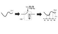
- the track mode Mt in which the output signal Vout follows the input signal Vin and the hold mode Mh in which the output signal Vout is held constant are held at the timing synchronized with the clock signal Vck. It is a circuit that repeats alternately.
- the track and hold circuit for the front end of the ADC takes some time for analog-to-digital conversion, so it is necessary to hold the input signal during the conversion. Because.
- Another reason for using the track and hold circuit in the front end of the ADC is to reduce the effects of noise due to clock jitter. Since the timing of the clock signals is not perfectly evenly spaced, there is statistical variation in the timing of holding the input signal. When there is such clock jitter, it is observed that noise is superimposed on the output of the ADC.
- the clock jitter is within the hold time of the track-and-hold circuit. If so, it will not be affected by noise.
- the most advanced ADCs in recent years cannot increase the speed while keeping the noise level within a practical range because it is difficult to reduce the clock jitter, and the clock jitter becomes a factor that hinders the increase in speed. There is. Therefore, increasing the speed of the track-and-hold circuit is effective in increasing the speed of the ADC.
- analog circuits are composed of connecting switching elements called transistors, resistors, capacitors, etc.
- transistors There are several types of transistors, but bipolar transistors are often used in analog circuits that require high-speed operation.
- a switched-emitter follower As a circuit configuration of an existing track-and-hold circuit using a bipolar transistor, what is called a switched-emitter follower is well known.
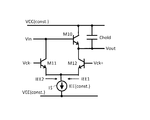
- FIG. 6 shows a typical configuration of a conventional track-and-hold circuit using a bipolar transistor.
- VCS and VEE are power supply voltages
- Vin is an input signal
- Vout is an output signal
- Vck + and Vck ⁇ are clock signals.
- the clock signals Vck + and Vck ⁇ are differential signals. Further, (const.) In FIG. 6 indicates that the voltage or current is constant regardless of time.
- the track-and-hold circuit is composed of bipolar transistors M10 to M12, a capacitor Hold, and a constant current source IS.
- the constant current source IS is often composed of a transistor or the like.
- FIGS. 7A to 7E The basic operation of the track-and-hold circuit of FIG. 6 will be described with reference to FIGS. 7A to 7E.
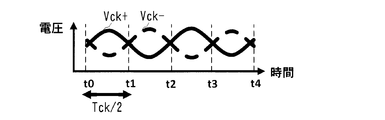
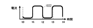
- the waveforms of the currents IEE1 and IEE2 when the differential clock signals Vck + and Vck ⁇ having a period of Tck shown in FIG. 7A and the input signal Vin shown in FIG. 7B are applied to the track and hold circuit are shown in FIG. 7C. , FIG. 7D, and the waveform of the output signal Vout is shown in FIG. 7E.
- T0, t1, t2, t3, and t4 in FIGS. 7A to 7E represent the time.
- t0 to t4 are lined up at regular intervals of Tck / 2.
- the output signal Vout is held at a constant value only while the clock signal is Low. .. That is, when the time t satisfies t1 ⁇ t ⁇ t2 or t3 ⁇ t ⁇ t4, the track and hold circuit is in the hold mode.
- the basic operation of the track-and-hold circuit is to alternately repeat the track mode and the hold mode according to the High / Low of the clock signal.
- the data rate of the track-and-hold circuit that is, the number of times data is acquired per unit time, depends on the clock frequency.
- there is an upper limit to the frequency of the clock signal that can be input due to the constraint conditions of the analog circuit, specifically, the parasitic resistance and the parasitic capacitance existing in the transistor and the wiring.
- the upper limit of the frequency of this clock signal is the main factor that limits the speed of the track-and-hold circuit.
- the present invention has been made to solve the above problems, and an object of the present invention is to increase the data rate of a track-and-hold circuit.
- the base is connected to the signal input terminal, the power supply voltage is applied to the collector, the emitter is connected to the first signal output terminal, and the base is the signal.
- a second transistor connected to an input terminal, the power supply voltage is applied to a collector, an emitter is connected to a second signal output terminal, one end is connected to the collector of the first transistor, and the other end is said.
- a first capacitor connected to the emitter of the first transistor, a second capacitor having one end connected to the collector of the second transistor and the other end connected to the emitter of the second transistor, and the above.
- a constant current source configured to supply a constant current to the first and second transistors is connected between the emitters of the first and second transistors and the constant current source to form a differential clock signal. It is characterized by including a switch circuit configured to alternately turn on the first and second transistors accordingly.
- the base is connected to the positive phase clock input terminal
- the collector is connected to the emitter of the first transistor
- the emitter is the fixed emitter.
- a third transistor connected to the current source and a fourth transistor whose base is connected to the antiphase clock input terminal, the collector is connected to the emitter of the second transistor, and the emitter is connected to the constant current source. It is characterized by being composed of.
- the base is connected to the positive phase signal input terminal, the power supply voltage is applied to the collector, and the emitter is connected to the first positive phase signal output terminal.
- a second transistor whose base is connected to the negative-phase signal input terminal, the power supply voltage is applied to the collector, and the emitter is connected to the first negative-phase signal output terminal, and the base is the positive-phase signal input terminal.
- a third transistor connected to the collector, the power supply voltage is applied to the collector, the emitter is connected to the second positive phase signal output terminal, and the base is connected to the negative phase signal input terminal, and the power supply voltage is connected to the collector.
- the emitter is connected to the second anti-phase signal output terminal
- the fourth transistor one end is connected to the collector of the first transistor, and the other end is connected to the emitter of the first transistor.
- the first capacitor one end connected to the collector of the second transistor, the other end connected to the emitter of the second transistor, and one end connected to the collector of the third transistor.
- a third capacitor connected and the other end connected to the emitter of the third transistor, one end connected to the collector of the fourth transistor, and the other end connected to the emitter of the fourth transistor.
- a fourth capacitor a constant current source configured to supply a constant current to the first, second, third, and fourth transistors, and the first, second, third, and fourth transistors.
- a second differential circuit composed of the first and second transistors and a second transistor composed of the third and fourth transistors, which are connected between the emitter and the constant current source and are composed of the first and second transistors according to the differential clock signal. It is characterized by including a switch circuit configured to alternately turn on the differential circuit of the above.
- the base is connected to the positive phase clock input terminal
- the collector is connected to the emitter of the first transistor
- the emitter is the constant.
- a fifth transistor connected to the current source, a base connected to the positive phase clock input terminal, a collector connected to the emitter of the second transistor, and a sixth transistor connected to the constant current source.
- a circuit that goes into track mode and a circuit that goes into hold mode are switched every half cycle of the differential clock signal. It is possible to realize a data rate twice as high as that of a conventional track-and-hold circuit.
- the first differential circuit composed of the first and second transistors and the second differential circuit composed of the third and fourth transistors are alternately turned on according to the differential clock signal.
- the differential circuit that goes into track mode and the differential circuit that goes into hold mode can be switched every half cycle of the clock signal, and the data rate is twice that of the conventional track-and-hold circuit. Can be realized.
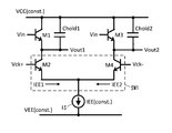
- FIG. 1 is a circuit diagram showing a configuration of a track-and-hold circuit according to a first embodiment of the present invention.
- 2A-2F are diagrams showing signal waveforms of each part of the track-and-hold circuit according to the first embodiment of the present invention.
- FIG. 3 is a circuit diagram showing a configuration of a track-and-hold circuit according to a second embodiment of the present invention.
- 4A-4G are diagrams showing signal waveforms of each part of the track-and-hold circuit according to the second embodiment of the present invention.
- FIG. 5 is a diagram conceptually explaining the configuration and operation of the track and hold circuit.
- FIG. 6 is a circuit diagram showing the configuration of a conventional track-and-hold circuit.
- 7A-7E are diagrams showing signal waveforms of each part of the conventional track and hold circuit.
- FIG. 1 is a circuit diagram showing a configuration of a track-and-hold circuit according to a first embodiment of the present invention.
- VCS and VEE are power supply voltages
- Vin is an input signal
- Vout is an output signal
- Vck + and Vck ⁇ are clock signals.
- the clock signals Vck + and Vck ⁇ are differential signals.
- (const.) In FIG. 1 indicates that the voltage or current is constant regardless of time.
- the base is connected to the signal input terminal (Vin), the power supply voltage VCS is applied to the collector, and the emitter is connected to the first signal output terminal (Vout1).
- the M1 and the bipolar transistor M2 whose base is connected to the positive phase clock input terminal (Vck +) and the collector is connected to the emitter of the bipolar transistor M1 and the base are connected to the signal input terminal (Vin), and the power supply voltage VCS is connected to the collector.
- the emitter was connected to the second signal output terminal (Vout2) of the bipolar transistor M3, the base was connected to the antiphase clock input terminal (Vck-), and the collector was connected to the emitter of the bipolar transistor M3. It includes a bipolar transistor M4.
- the track-and-hold circuit has a capacitor Hold1 having one end connected to the collector of the bipolar transistor M1 and the other end connected to the emitter of the bipolar transistor M1 and one end connected to the collector of the bipolar transistor M3. Holds a capacitor Hold2 connected to the emitter of the bipolar transistor M3, and a constant current source IS having one end connected to the emitters of the bipolar transistors M2 and M4 and the other end connected to the power supply voltage VEE.
- the constant current source IS is often composed of a transistor or the like.
- the transistors M2 and M4 constitute a switch circuit SW1 that alternately turns on the transistors M1 and M2 according to the differential clock signals Vck + and Vck ⁇ .
- FIGS. 2A to 2F The basic operation of the track-and-hold circuit of FIG. 1 will be described with reference to FIGS. 2A to 2F.
- the waveforms of the currents IEE1 and IEE2 when the differential clock signals Vck + and Vck ⁇ having a period Tck shown in FIG. 2A and the input signals Vin shown in FIG. 2B are applied to the track and hold circuit are shown in FIG. 2C. , 2D, and the waveforms of the output signals Vout1 and Vout2 are shown in FIGS. 2E and 2F.
- T0, t1, t2, t3, and t4 in FIGS. 2A to 2F represent the time.
- t0 to t4 are lined up at regular intervals of Tck / 2.
- the first circuit including the transistor M1 and the capacitor Hold1 is in the track mode, and the transistor M3
- the second circuit including the capacitor Clock2 is in the hold mode.
- the circuit in the track mode and the circuit in the hold mode are replaced every half cycle Tck / 2 of the clock signal. Can be done.
- the parasitic resistance and parasitic capacitance existing in the transistor and wiring are the same as in the conventional circuit configuration, so the upper limit of the input clock frequency is the same as in the conventional one.
- the circuit that enters the track mode and the circuit that enters the hold mode change every half cycle Tck / 2 of the clock signal, so that a clock signal having the same frequency is used as compared with the conventional circuit configuration shown in FIG.
- the input signal can be acquired at half the time interval, so the data rate can be doubled. Therefore, according to this embodiment, the speed of the track-and-hold circuit can be increased.
- an ADC that inputs the output signal Vout1 and an ADC that inputs the output terminal Vout2 are separately provided and output from the two ADCs.
- the digital signals to be generated may be synthesized.
- a multiplexer is provided between the track and hold circuit of this embodiment and one ADC, and the output signal of the output signals Vout1 and Vout2, which is in the hold mode state in synchronization with the clock signal, is always selected. Then, the multiplexer may be switched so as to output to the ADC.
- FIG. 3 is a circuit diagram showing a configuration of a track-and-hold circuit according to a second embodiment of the present invention.
- the base is connected to the positive-phase signal input terminal (Vin +)
- the power supply voltage VCS is applied to the collector
- the emitter is connected to the first positive-phase signal output terminal (Vout1 +).
- the bipolar transistor M1 and the base are connected to the positive phase clock input terminal (Vck +)
- the collector is connected to the emitter of the bipolar transistor M1, the bipolar transistor M2, and the base is connected to the positive phase signal input terminal (Vin +).
- the power supply voltage VCS is applied to the collector, the emitter is connected to the second positive phase signal output terminal (Vout2 +), the bipolar transistor M3, and the base is connected to the reverse phase clock input terminal (Vck-), and the collector is bipolar.
- the bipolar transistor M4 connected to the emitter of the transistor M3 and the base are connected to the anti-phase signal input terminal (Vin-), the power supply voltage VCS is applied to the collector, and the emitter is the first anti-phase signal output terminal (Vout1-).
- the bipolar transistor M6 whose base is connected to the positive phase clock input terminal (Vck +) and the collector connected to the emitter of the bipolar transistor M5, and the base is the negative phase signal input terminal (Vin-).
- the power supply voltage VCS is applied to the collector, the emitter is connected to the second anti-phase signal output terminal (Vout2-), and the base is connected to the anti-phase clock input terminal (Vck-).
- the collector is provided with a bipolar transistor M8 connected to the emitter of the bipolar transistor M7.
- the track-and-hold circuit has a capacitor Hold1 having one end connected to the collector of the bipolar transistor M1 and the other end connected to the emitter of the bipolar transistor M1 and one end connected to the collector of the bipolar transistor M3. Is connected to the capacitor Hold2 connected to the emitter of the bipolar transistor M3, one end is connected to the collector of the bipolar transistor M5, the other end is connected to the capacitor Hold3 connected to the emitter of the bipolar transistor M5, and one end is connected to the collector of the bipolar transistor M7. The other end is connected to the emitter of the bipolar transistor M7, and the other end is connected to the emitter of the bipolar transistors M2, M4, M6, M8, and the other end is connected to the power supply voltage VEE. It has.
- the transistors M2, M4, M6, and M8 alternately alternate between a first differential circuit composed of transistors M1 and M5 and a second differential circuit composed of transistors M3 and M7 according to the differential clock signals Vck + and Vck ⁇ .
- the switch circuit SW2 for turning on is configured.
- FIGS. 4A to 4F The basic operation of the track-and-hold circuit of FIG. 3 will be described with reference to FIGS. 4A to 4F.
- the waveforms of the dynamic output signals Vout1 + and Vout1- are shown in FIGS. 4D and 4E, and the waveforms of the differential output signals Vout2 + and Vout2- are shown in FIGS. 4F and 4G.
- the output signal Vout2- is held at a constant value only while the clock signal is High. Will be done.
- the first differential circuit including the transistors M1 and M5 and the capacitors Hold1 and Hold3 is a track.
- the mode is set, and the second differential circuit including the transistors M3 and M7 and the capacitors Hold2 and Hold4 is in the hold mode.
- the differential circuit in the track mode and the differential circuit in the hold mode are half of the clock signal. It can be changed every 2 cycles Tck / 2.
- connection form between the track and hold circuit and the ADC in the subsequent stage is the same as in the first embodiment.
- a differential input type ADC that inputs the differential output signals Vout1 + and Vout1-
- a differential input type ADC that inputs the differential output signals Vout2 + and Vout2- are used. It may be provided.
- a differential input differential output type that selects and outputs the differential output signal Vout1 +, Vout1- and the differential output signals Vout2 +, Vout2-, whichever is in the hold mode state.
- the multiplexer and the differential input type ADC that receives the differential output signal of the multiplexer as input may be provided.
- a differential input single-phase output type that converts the differential output signal of the differential output signals Vout1 +, Vout1- and the differential output signals Vout2 +, Vout2-, which is in the hold mode state, into a single-phase signal and outputs the signal.
- a multiplexer and a single-phase input type ADC that receives the output signal of the multiplexer as an input may be provided.
- the present invention can be applied to a track and hold circuit.
- M1 to M8 Bipolar transistor, Hold1 to Hold4 ... Capacitor, IS ... Constant current source, SW1, SW2 ... Switch circuit.
Landscapes
- Engineering & Computer Science (AREA)
- Theoretical Computer Science (AREA)
- Electronic Switches (AREA)
- Analogue/Digital Conversion (AREA)
- Manipulation Of Pulses (AREA)
Priority Applications (3)
| Application Number | Priority Date | Filing Date | Title |
|---|---|---|---|
| PCT/JP2020/002895 WO2021152687A1 (ja) | 2020-01-28 | 2020-01-28 | トラック・アンド・ホールド回路 |
| US17/793,628 US11830560B2 (en) | 2020-01-28 | 2020-01-28 | Track-and-hold circuit |
| JP2021573658A JP7331956B2 (ja) | 2020-01-28 | 2020-01-28 | トラック・アンド・ホールド回路 |
Applications Claiming Priority (1)
| Application Number | Priority Date | Filing Date | Title |
|---|---|---|---|
| PCT/JP2020/002895 WO2021152687A1 (ja) | 2020-01-28 | 2020-01-28 | トラック・アンド・ホールド回路 |
Publications (1)
| Publication Number | Publication Date |
|---|---|
| WO2021152687A1 true WO2021152687A1 (ja) | 2021-08-05 |
Family
ID=77078050
Family Applications (1)
| Application Number | Title | Priority Date | Filing Date |
|---|---|---|---|
| PCT/JP2020/002895 Ceased WO2021152687A1 (ja) | 2020-01-28 | 2020-01-28 | トラック・アンド・ホールド回路 |
Country Status (3)
| Country | Link |
|---|---|
| US (1) | US11830560B2 (https=) |
| JP (1) | JP7331956B2 (https=) |
| WO (1) | WO2021152687A1 (https=) |
Cited By (1)
| Publication number | Priority date | Publication date | Assignee | Title |
|---|---|---|---|---|
| WO2026003918A1 (ja) * | 2024-06-24 | 2026-01-02 | Ntt株式会社 | トラック・アンド・ホールド回路 |
Families Citing this family (1)
| Publication number | Priority date | Publication date | Assignee | Title |
|---|---|---|---|---|
| WO2021205592A1 (ja) * | 2020-04-09 | 2021-10-14 | 日本電信電話株式会社 | スイッチト・エミッタ・フォロワ回路 |
Citations (5)
| Publication number | Priority date | Publication date | Assignee | Title |
|---|---|---|---|---|
| JPH0729391A (ja) * | 1993-07-08 | 1995-01-31 | Fujitsu Ltd | サンプルホールド回路 |
| JPH1092190A (ja) * | 1996-06-21 | 1998-04-10 | General Motors Corp <Gm> | 追跡および保持回路 |
| JP2009230842A (ja) * | 2008-02-27 | 2009-10-08 | Yokogawa Electric Corp | サンプルホールド回路 |
| JP2017153021A (ja) * | 2016-02-26 | 2017-08-31 | 日本電信電話株式会社 | トラック・アンド・ホールド回路 |
| WO2019172171A1 (ja) * | 2018-03-08 | 2019-09-12 | 日本電信電話株式会社 | トラックアンドホールド回路 |
Family Cites Families (2)
| Publication number | Priority date | Publication date | Assignee | Title |
|---|---|---|---|---|
| US6028459A (en) * | 1998-04-20 | 2000-02-22 | National Semiconductor Corporation | Track and hold circuit with clamp |
| JP4247181B2 (ja) * | 2004-11-30 | 2009-04-02 | 富士通株式会社 | サンプルホールド回路 |
-
2020
- 2020-01-28 US US17/793,628 patent/US11830560B2/en active Active
- 2020-01-28 JP JP2021573658A patent/JP7331956B2/ja active Active
- 2020-01-28 WO PCT/JP2020/002895 patent/WO2021152687A1/ja not_active Ceased
Patent Citations (5)
| Publication number | Priority date | Publication date | Assignee | Title |
|---|---|---|---|---|
| JPH0729391A (ja) * | 1993-07-08 | 1995-01-31 | Fujitsu Ltd | サンプルホールド回路 |
| JPH1092190A (ja) * | 1996-06-21 | 1998-04-10 | General Motors Corp <Gm> | 追跡および保持回路 |
| JP2009230842A (ja) * | 2008-02-27 | 2009-10-08 | Yokogawa Electric Corp | サンプルホールド回路 |
| JP2017153021A (ja) * | 2016-02-26 | 2017-08-31 | 日本電信電話株式会社 | トラック・アンド・ホールド回路 |
| WO2019172171A1 (ja) * | 2018-03-08 | 2019-09-12 | 日本電信電話株式会社 | トラックアンドホールド回路 |
Cited By (1)
| Publication number | Priority date | Publication date | Assignee | Title |
|---|---|---|---|---|
| WO2026003918A1 (ja) * | 2024-06-24 | 2026-01-02 | Ntt株式会社 | トラック・アンド・ホールド回路 |
Also Published As
| Publication number | Publication date |
|---|---|
| US11830560B2 (en) | 2023-11-28 |
| US20230048012A1 (en) | 2023-02-16 |
| JP7331956B2 (ja) | 2023-08-23 |
| JPWO2021152687A1 (https=) | 2021-08-05 |
Similar Documents
| Publication | Publication Date | Title |
|---|---|---|
| VorenKamp et al. | A 12-b, 60-MSample/s cascaded folding and interpolating ADC | |
| US11095300B2 (en) | Reduced noise dynamic comparator for a successive approximation register analog-to-digital converter | |
| CN102142840B (zh) | 折叠模数转换器 | |
| US7782096B2 (en) | Track-and-hold circuit with low distortion | |
| US9413373B1 (en) | Amplifier circuit and pipeline type analog-digital converter | |
| CN101346880A (zh) | 比较器和a/d转换器 | |
| US12418293B2 (en) | Operation stage of pipeline analog-to-digital converter (ADC) and multiplying circuit thereof | |
| EP2051382B1 (en) | Folding circuit and analog-to-digital converter | |
| JP7331956B2 (ja) | トラック・アンド・ホールド回路 | |
| JP2004312555A (ja) | コンパレータ、差動増幅器、2段増幅器及びアナログ/ディジタル変換器 | |
| WO2009009420A2 (en) | Low glitch offset correction circuit for auto-zero sensor amplifiers and method | |
| US7403149B2 (en) | Folding and interpolating analog-to-digital converter and method of converting analog signal to digital signal | |
| US20120286986A1 (en) | A/d conversion circuit | |
| US7098829B2 (en) | Digital to analog conversion | |
| JP3326619B2 (ja) | Pwm回路 | |
| US20090219060A1 (en) | Method and apparatus of sfdr enhancement | |
| US8941414B2 (en) | Track-and-hold circuit with low distortion | |
| JPS59104827A (ja) | アナログ−デジタル変換用集積回路 | |
| CN1271788C (zh) | 采用改进型折叠电路的模数转换器 | |
| JP7444244B2 (ja) | トラック・アンド・ホールド回路 | |
| JP7375916B2 (ja) | スイッチト・エミッタ・フォロワ回路 | |
| EP1271781B1 (en) | Comparator circuit | |
| US10523231B1 (en) | Dynamic integrator with boosted output impedance of the transconductance | |
| Boni et al. | 3.3-V, 200-Ms/s BiCMOS comparator for current-mode interpolation using a transconductance stage |
Legal Events
| Date | Code | Title | Description |
|---|---|---|---|
| 121 | Ep: the epo has been informed by wipo that ep was designated in this application |
Ref document number: 20916844 Country of ref document: EP Kind code of ref document: A1 |
|
| ENP | Entry into the national phase |
Ref document number: 2021573658 Country of ref document: JP Kind code of ref document: A |
|
| NENP | Non-entry into the national phase |
Ref country code: DE |
|
| 122 | Ep: pct application non-entry in european phase |
Ref document number: 20916844 Country of ref document: EP Kind code of ref document: A1 |