WO2021152687A1 - Track and hold circuit - Google Patents
Track and hold circuit Download PDFInfo
- Publication number
- WO2021152687A1 WO2021152687A1 PCT/JP2020/002895 JP2020002895W WO2021152687A1 WO 2021152687 A1 WO2021152687 A1 WO 2021152687A1 JP 2020002895 W JP2020002895 W JP 2020002895W WO 2021152687 A1 WO2021152687 A1 WO 2021152687A1
- Authority
- WO
- WIPO (PCT)
- Prior art keywords
- transistor
- emitter
- collector
- track
- constant current
- Prior art date
Links
Images


Classifications
-
- G—PHYSICS
- G11—INFORMATION STORAGE
- G11C—STATIC STORES
- G11C27/00—Electric analogue stores, e.g. for storing instantaneous values
- G11C27/02—Sample-and-hold arrangements
-
- G—PHYSICS
- G11—INFORMATION STORAGE
- G11C—STATIC STORES
- G11C27/00—Electric analogue stores, e.g. for storing instantaneous values
- G11C27/02—Sample-and-hold arrangements
- G11C27/024—Sample-and-hold arrangements using a capacitive memory element
- G11C27/028—Current mode circuits, e.g. switched current memories
-
- H—ELECTRICITY
- H03—ELECTRONIC CIRCUITRY
- H03K—PULSE TECHNIQUE
- H03K17/00—Electronic switching or gating, i.e. not by contact-making and –breaking
- H03K17/51—Electronic switching or gating, i.e. not by contact-making and –breaking characterised by the components used
- H03K17/56—Electronic switching or gating, i.e. not by contact-making and –breaking characterised by the components used by the use, as active elements, of semiconductor devices
- H03K17/60—Electronic switching or gating, i.e. not by contact-making and –breaking characterised by the components used by the use, as active elements, of semiconductor devices the devices being bipolar transistors
- H03K17/62—Switching arrangements with several input- output-terminals, e.g. multiplexers, distributors
- H03K17/6285—Switching arrangements with several input- output-terminals, e.g. multiplexers, distributors with several outputs only combined with selecting means
-
- H—ELECTRICITY
- H03—ELECTRONIC CIRCUITRY
- H03M—CODING; DECODING; CODE CONVERSION IN GENERAL
- H03M1/00—Analogue/digital conversion; Digital/analogue conversion
- H03M1/12—Analogue/digital converters
- H03M1/124—Sampling or signal conditioning arrangements specially adapted for A/D converters
Definitions
- the present invention relates to a track-and-hold circuit that alternately repeats a track mode and a hold mode at a timing synchronized with a clock signal.
- Analog-to-digital converter (ADC: Analog-to-Digital Converter) is a device widely used for communication, measurement, etc.
- the ADC converts the input voltage, which is an analog signal, into a quantized digital value at the timing synchronized with the clock signal, and outputs the digital code.
- the ADC has a track-and-hold circuit at the front end portion (see Non-Patent Document 1).
- the track mode Mt in which the output signal Vout follows the input signal Vin and the hold mode Mh in which the output signal Vout is held constant are held at the timing synchronized with the clock signal Vck. It is a circuit that repeats alternately.
- the track and hold circuit for the front end of the ADC takes some time for analog-to-digital conversion, so it is necessary to hold the input signal during the conversion. Because.
- Another reason for using the track and hold circuit in the front end of the ADC is to reduce the effects of noise due to clock jitter. Since the timing of the clock signals is not perfectly evenly spaced, there is statistical variation in the timing of holding the input signal. When there is such clock jitter, it is observed that noise is superimposed on the output of the ADC.
- the clock jitter is within the hold time of the track-and-hold circuit. If so, it will not be affected by noise.
- the most advanced ADCs in recent years cannot increase the speed while keeping the noise level within a practical range because it is difficult to reduce the clock jitter, and the clock jitter becomes a factor that hinders the increase in speed. There is. Therefore, increasing the speed of the track-and-hold circuit is effective in increasing the speed of the ADC.
- analog circuits are composed of connecting switching elements called transistors, resistors, capacitors, etc.
- transistors There are several types of transistors, but bipolar transistors are often used in analog circuits that require high-speed operation.
- a switched-emitter follower As a circuit configuration of an existing track-and-hold circuit using a bipolar transistor, what is called a switched-emitter follower is well known.
- FIG. 6 shows a typical configuration of a conventional track-and-hold circuit using a bipolar transistor.
- VCS and VEE are power supply voltages
- Vin is an input signal
- Vout is an output signal
- Vck + and Vck ⁇ are clock signals.
- the clock signals Vck + and Vck ⁇ are differential signals. Further, (const.) In FIG. 6 indicates that the voltage or current is constant regardless of time.
- the track-and-hold circuit is composed of bipolar transistors M10 to M12, a capacitor Hold, and a constant current source IS.
- the constant current source IS is often composed of a transistor or the like.
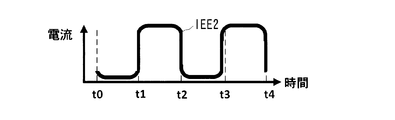
- FIGS. 7A to 7E The basic operation of the track-and-hold circuit of FIG. 6 will be described with reference to FIGS. 7A to 7E.
- the waveforms of the currents IEE1 and IEE2 when the differential clock signals Vck + and Vck ⁇ having a period of Tck shown in FIG. 7A and the input signal Vin shown in FIG. 7B are applied to the track and hold circuit are shown in FIG. 7C. , FIG. 7D, and the waveform of the output signal Vout is shown in FIG. 7E.
- T0, t1, t2, t3, and t4 in FIGS. 7A to 7E represent the time.
- t0 to t4 are lined up at regular intervals of Tck / 2.
- the output signal Vout is held at a constant value only while the clock signal is Low. .. That is, when the time t satisfies t1 ⁇ t ⁇ t2 or t3 ⁇ t ⁇ t4, the track and hold circuit is in the hold mode.
- the basic operation of the track-and-hold circuit is to alternately repeat the track mode and the hold mode according to the High / Low of the clock signal.
- the data rate of the track-and-hold circuit that is, the number of times data is acquired per unit time, depends on the clock frequency.
- there is an upper limit to the frequency of the clock signal that can be input due to the constraint conditions of the analog circuit, specifically, the parasitic resistance and the parasitic capacitance existing in the transistor and the wiring.
- the upper limit of the frequency of this clock signal is the main factor that limits the speed of the track-and-hold circuit.
- the present invention has been made to solve the above problems, and an object of the present invention is to increase the data rate of a track-and-hold circuit.
- the base is connected to the signal input terminal, the power supply voltage is applied to the collector, the emitter is connected to the first signal output terminal, and the base is the signal.
- a second transistor connected to an input terminal, the power supply voltage is applied to a collector, an emitter is connected to a second signal output terminal, one end is connected to the collector of the first transistor, and the other end is said.
- a first capacitor connected to the emitter of the first transistor, a second capacitor having one end connected to the collector of the second transistor and the other end connected to the emitter of the second transistor, and the above.
- a constant current source configured to supply a constant current to the first and second transistors is connected between the emitters of the first and second transistors and the constant current source to form a differential clock signal. It is characterized by including a switch circuit configured to alternately turn on the first and second transistors accordingly.
- the base is connected to the positive phase clock input terminal
- the collector is connected to the emitter of the first transistor
- the emitter is the fixed emitter.
- a third transistor connected to the current source and a fourth transistor whose base is connected to the antiphase clock input terminal, the collector is connected to the emitter of the second transistor, and the emitter is connected to the constant current source. It is characterized by being composed of.
- the base is connected to the positive phase signal input terminal, the power supply voltage is applied to the collector, and the emitter is connected to the first positive phase signal output terminal.
- a second transistor whose base is connected to the negative-phase signal input terminal, the power supply voltage is applied to the collector, and the emitter is connected to the first negative-phase signal output terminal, and the base is the positive-phase signal input terminal.
- a third transistor connected to the collector, the power supply voltage is applied to the collector, the emitter is connected to the second positive phase signal output terminal, and the base is connected to the negative phase signal input terminal, and the power supply voltage is connected to the collector.
- the emitter is connected to the second anti-phase signal output terminal
- the fourth transistor one end is connected to the collector of the first transistor, and the other end is connected to the emitter of the first transistor.
- the first capacitor one end connected to the collector of the second transistor, the other end connected to the emitter of the second transistor, and one end connected to the collector of the third transistor.
- a third capacitor connected and the other end connected to the emitter of the third transistor, one end connected to the collector of the fourth transistor, and the other end connected to the emitter of the fourth transistor.
- a fourth capacitor a constant current source configured to supply a constant current to the first, second, third, and fourth transistors, and the first, second, third, and fourth transistors.
- a second differential circuit composed of the first and second transistors and a second transistor composed of the third and fourth transistors, which are connected between the emitter and the constant current source and are composed of the first and second transistors according to the differential clock signal. It is characterized by including a switch circuit configured to alternately turn on the differential circuit of the above.
- the base is connected to the positive phase clock input terminal
- the collector is connected to the emitter of the first transistor
- the emitter is the constant.
- a fifth transistor connected to the current source, a base connected to the positive phase clock input terminal, a collector connected to the emitter of the second transistor, and a sixth transistor connected to the constant current source.
- a circuit that goes into track mode and a circuit that goes into hold mode are switched every half cycle of the differential clock signal. It is possible to realize a data rate twice as high as that of a conventional track-and-hold circuit.
- the first differential circuit composed of the first and second transistors and the second differential circuit composed of the third and fourth transistors are alternately turned on according to the differential clock signal.
- the differential circuit that goes into track mode and the differential circuit that goes into hold mode can be switched every half cycle of the clock signal, and the data rate is twice that of the conventional track-and-hold circuit. Can be realized.
- FIG. 1 is a circuit diagram showing a configuration of a track-and-hold circuit according to a first embodiment of the present invention.
- 2A-2F are diagrams showing signal waveforms of each part of the track-and-hold circuit according to the first embodiment of the present invention.
- FIG. 3 is a circuit diagram showing a configuration of a track-and-hold circuit according to a second embodiment of the present invention.
- 4A-4G are diagrams showing signal waveforms of each part of the track-and-hold circuit according to the second embodiment of the present invention.
- FIG. 5 is a diagram conceptually explaining the configuration and operation of the track and hold circuit.
- FIG. 6 is a circuit diagram showing the configuration of a conventional track-and-hold circuit.
- 7A-7E are diagrams showing signal waveforms of each part of the conventional track and hold circuit.
- FIG. 1 is a circuit diagram showing a configuration of a track-and-hold circuit according to a first embodiment of the present invention.
- VCS and VEE are power supply voltages
- Vin is an input signal
- Vout is an output signal
- Vck + and Vck ⁇ are clock signals.
- the clock signals Vck + and Vck ⁇ are differential signals.
- (const.) In FIG. 1 indicates that the voltage or current is constant regardless of time.
- the base is connected to the signal input terminal (Vin), the power supply voltage VCS is applied to the collector, and the emitter is connected to the first signal output terminal (Vout1).
- the M1 and the bipolar transistor M2 whose base is connected to the positive phase clock input terminal (Vck +) and the collector is connected to the emitter of the bipolar transistor M1 and the base are connected to the signal input terminal (Vin), and the power supply voltage VCS is connected to the collector.
- the emitter was connected to the second signal output terminal (Vout2) of the bipolar transistor M3, the base was connected to the antiphase clock input terminal (Vck-), and the collector was connected to the emitter of the bipolar transistor M3. It includes a bipolar transistor M4.
- the track-and-hold circuit has a capacitor Hold1 having one end connected to the collector of the bipolar transistor M1 and the other end connected to the emitter of the bipolar transistor M1 and one end connected to the collector of the bipolar transistor M3. Holds a capacitor Hold2 connected to the emitter of the bipolar transistor M3, and a constant current source IS having one end connected to the emitters of the bipolar transistors M2 and M4 and the other end connected to the power supply voltage VEE.
- the constant current source IS is often composed of a transistor or the like.
- the transistors M2 and M4 constitute a switch circuit SW1 that alternately turns on the transistors M1 and M2 according to the differential clock signals Vck + and Vck ⁇ .
- FIGS. 2A to 2F The basic operation of the track-and-hold circuit of FIG. 1 will be described with reference to FIGS. 2A to 2F.
- the waveforms of the currents IEE1 and IEE2 when the differential clock signals Vck + and Vck ⁇ having a period Tck shown in FIG. 2A and the input signals Vin shown in FIG. 2B are applied to the track and hold circuit are shown in FIG. 2C. , 2D, and the waveforms of the output signals Vout1 and Vout2 are shown in FIGS. 2E and 2F.
- T0, t1, t2, t3, and t4 in FIGS. 2A to 2F represent the time.
- t0 to t4 are lined up at regular intervals of Tck / 2.
- the first circuit including the transistor M1 and the capacitor Hold1 is in the track mode, and the transistor M3
- the second circuit including the capacitor Clock2 is in the hold mode.
- the circuit in the track mode and the circuit in the hold mode are replaced every half cycle Tck / 2 of the clock signal. Can be done.
- the parasitic resistance and parasitic capacitance existing in the transistor and wiring are the same as in the conventional circuit configuration, so the upper limit of the input clock frequency is the same as in the conventional one.
- the circuit that enters the track mode and the circuit that enters the hold mode change every half cycle Tck / 2 of the clock signal, so that a clock signal having the same frequency is used as compared with the conventional circuit configuration shown in FIG.
- the input signal can be acquired at half the time interval, so the data rate can be doubled. Therefore, according to this embodiment, the speed of the track-and-hold circuit can be increased.
- an ADC that inputs the output signal Vout1 and an ADC that inputs the output terminal Vout2 are separately provided and output from the two ADCs.
- the digital signals to be generated may be synthesized.
- a multiplexer is provided between the track and hold circuit of this embodiment and one ADC, and the output signal of the output signals Vout1 and Vout2, which is in the hold mode state in synchronization with the clock signal, is always selected. Then, the multiplexer may be switched so as to output to the ADC.
- FIG. 3 is a circuit diagram showing a configuration of a track-and-hold circuit according to a second embodiment of the present invention.
- the base is connected to the positive-phase signal input terminal (Vin +)
- the power supply voltage VCS is applied to the collector
- the emitter is connected to the first positive-phase signal output terminal (Vout1 +).
- the bipolar transistor M1 and the base are connected to the positive phase clock input terminal (Vck +)
- the collector is connected to the emitter of the bipolar transistor M1, the bipolar transistor M2, and the base is connected to the positive phase signal input terminal (Vin +).
- the power supply voltage VCS is applied to the collector, the emitter is connected to the second positive phase signal output terminal (Vout2 +), the bipolar transistor M3, and the base is connected to the reverse phase clock input terminal (Vck-), and the collector is bipolar.
- the bipolar transistor M4 connected to the emitter of the transistor M3 and the base are connected to the anti-phase signal input terminal (Vin-), the power supply voltage VCS is applied to the collector, and the emitter is the first anti-phase signal output terminal (Vout1-).
- the bipolar transistor M6 whose base is connected to the positive phase clock input terminal (Vck +) and the collector connected to the emitter of the bipolar transistor M5, and the base is the negative phase signal input terminal (Vin-).
- the power supply voltage VCS is applied to the collector, the emitter is connected to the second anti-phase signal output terminal (Vout2-), and the base is connected to the anti-phase clock input terminal (Vck-).
- the collector is provided with a bipolar transistor M8 connected to the emitter of the bipolar transistor M7.
- the track-and-hold circuit has a capacitor Hold1 having one end connected to the collector of the bipolar transistor M1 and the other end connected to the emitter of the bipolar transistor M1 and one end connected to the collector of the bipolar transistor M3. Is connected to the capacitor Hold2 connected to the emitter of the bipolar transistor M3, one end is connected to the collector of the bipolar transistor M5, the other end is connected to the capacitor Hold3 connected to the emitter of the bipolar transistor M5, and one end is connected to the collector of the bipolar transistor M7. The other end is connected to the emitter of the bipolar transistor M7, and the other end is connected to the emitter of the bipolar transistors M2, M4, M6, M8, and the other end is connected to the power supply voltage VEE. It has.
- the transistors M2, M4, M6, and M8 alternately alternate between a first differential circuit composed of transistors M1 and M5 and a second differential circuit composed of transistors M3 and M7 according to the differential clock signals Vck + and Vck ⁇ .
- the switch circuit SW2 for turning on is configured.
- FIGS. 4A to 4F The basic operation of the track-and-hold circuit of FIG. 3 will be described with reference to FIGS. 4A to 4F.
- the waveforms of the dynamic output signals Vout1 + and Vout1- are shown in FIGS. 4D and 4E, and the waveforms of the differential output signals Vout2 + and Vout2- are shown in FIGS. 4F and 4G.
- the output signal Vout2- is held at a constant value only while the clock signal is High. Will be done.
- the first differential circuit including the transistors M1 and M5 and the capacitors Hold1 and Hold3 is a track.
- the mode is set, and the second differential circuit including the transistors M3 and M7 and the capacitors Hold2 and Hold4 is in the hold mode.
- the differential circuit in the track mode and the differential circuit in the hold mode are half of the clock signal. It can be changed every 2 cycles Tck / 2.
- connection form between the track and hold circuit and the ADC in the subsequent stage is the same as in the first embodiment.
- a differential input type ADC that inputs the differential output signals Vout1 + and Vout1-
- a differential input type ADC that inputs the differential output signals Vout2 + and Vout2- are used. It may be provided.
- a differential input differential output type that selects and outputs the differential output signal Vout1 +, Vout1- and the differential output signals Vout2 +, Vout2-, whichever is in the hold mode state.
- the multiplexer and the differential input type ADC that receives the differential output signal of the multiplexer as input may be provided.
- a differential input single-phase output type that converts the differential output signal of the differential output signals Vout1 +, Vout1- and the differential output signals Vout2 +, Vout2-, which is in the hold mode state, into a single-phase signal and outputs the signal.
- a multiplexer and a single-phase input type ADC that receives the output signal of the multiplexer as an input may be provided.
- the present invention can be applied to a track and hold circuit.
- M1 to M8 Bipolar transistor, Hold1 to Hold4 ... Capacitor, IS ... Constant current source, SW1, SW2 ... Switch circuit.
Abstract
This track and hold circuit comprises: a transistor (M1) in which a base is connected to a signal input terminal (Vin), a power source voltage (VCC) is applied to a collector, and an emitter is connected to a first signal output terminal (Vout1); a transistor (M3) in which a base is connected to the signal input terminal (Vin), the power source voltage (VCC) is applied to a collector, and an emitter is connected to a second signal output terminal (Vout2); capacitors (Chold1, Chold2); a constant current source (IS); and a switching circuit (SW1) that turns the transistors (M1, M3) on alternately in response to a differential clock signal (Vck+, Vck-).
Description
本発明は、クロック信号に同期したタイミングでトラックモードとホールドモードとを交互に繰り返すトラック・アンド・ホールド回路に関するものである。
The present invention relates to a track-and-hold circuit that alternately repeats a track mode and a hold mode at a timing synchronized with a clock signal.
アナログ-デジタル変換器(ADC:Analog-to-Digital Converter)は、通信、計測などに広く使われているデバイスである。ADCは、クロック信号に同期したタイミングでアナログ信号である入力電圧を、量子化されたデジタル値に変換し、そのデジタルコードを出力する。ADCは、多くの場合、フロントエンド部にトラック・アンド・ホールド回路を備えている(非特許文献1参照)。
Analog-to-digital converter (ADC: Analog-to-Digital Converter) is a device widely used for communication, measurement, etc. The ADC converts the input voltage, which is an analog signal, into a quantized digital value at the timing synchronized with the clock signal, and outputs the digital code. In many cases, the ADC has a track-and-hold circuit at the front end portion (see Non-Patent Document 1).
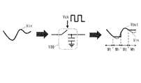
図5に示すように、トラック・アンド・ホールド回路100は、クロック信号Vckに同期したタイミングで、出力信号Voutが入力信号Vinに追従するトラックモードMtと出力信号Voutを一定に保持するホールドモードMhとを交互に繰り返す回路である。
As shown in FIG. 5, in the track-and-hold circuit 100, the track mode Mt in which the output signal Vout follows the input signal Vin and the hold mode Mh in which the output signal Vout is held constant are held at the timing synchronized with the clock signal Vck. It is a circuit that repeats alternately.
トラック・アンド・ホールド回路をADCのフロントエンド部に用いる理由の一つは、ADCがアナログ-デジタル変換のためにある程度の時間を要するため、変換の間、入力信号を保持しておく必要があるためである。
トラック・アンド・ホールド回路をADCのフロントエンド部に用いる他の理由は、クロックジッタによる雑音の影響を軽減するためである。クロック信号のタイミングが完全な等間隔でないために、入力信号を保持するタイミングに統計的なばらつきが生じる。このようなクロックジッタがあると、ADCの出力に雑音が重畳されたように観測される。 One of the reasons for using the track and hold circuit for the front end of the ADC is that the ADC takes some time for analog-to-digital conversion, so it is necessary to hold the input signal during the conversion. Because.
Another reason for using the track and hold circuit in the front end of the ADC is to reduce the effects of noise due to clock jitter. Since the timing of the clock signals is not perfectly evenly spaced, there is statistical variation in the timing of holding the input signal. When there is such clock jitter, it is observed that noise is superimposed on the output of the ADC.
クロックジッタの非常に少ないトラック・アンド・ホールド回路をフロントエンド部に用いることで、後段のADCでクロックジッタが多少発生したとしても、クロックジッタがトラック・アンド・ホールド回路のホールド時間内に収まっていれば雑音の影響は受けない。
特に近年の最先端のADCは、クロックジッタを下げることが困難なために、雑音レベルを実用的な範囲に抑えつつ高速化することができず、クロックジッタが高速化を阻害する要因となっている。そのため、トラック・アンド・ホールド回路の高速化はADCの高速化に有効である。 By using a track-and-hold circuit with very little clock jitter in the front-end section, even if some clock jitter occurs in the subsequent ADC, the clock jitter is within the hold time of the track-and-hold circuit. If so, it will not be affected by noise.
In particular, the most advanced ADCs in recent years cannot increase the speed while keeping the noise level within a practical range because it is difficult to reduce the clock jitter, and the clock jitter becomes a factor that hinders the increase in speed. There is. Therefore, increasing the speed of the track-and-hold circuit is effective in increasing the speed of the ADC.
多くの場合、アナログ回路は、トランジスタと呼ばれるスイッチング素子、抵抗、キャパシタ等を接続することで構成される。トランジスタにも何種類かあるが、高速な動作が求められるアナログ回路においてはバイポーラトランジスタがよく使われる。バイポーラトランジスタを用いた、既存のトラック・アンド・ホールド回路の回路構成として、スイッチト・エミッタ・フォロワと呼ばれるものがよく知られている。
In many cases, analog circuits are composed of connecting switching elements called transistors, resistors, capacitors, etc. There are several types of transistors, but bipolar transistors are often used in analog circuits that require high-speed operation. As a circuit configuration of an existing track-and-hold circuit using a bipolar transistor, what is called a switched-emitter follower is well known.
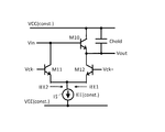
バイポーラトランジスタを用いた従来のトラック・アンド・ホールド回路の典型的な構成を図6に示す。図6のVCC,VEEは電源電圧、Vinは入力信号、Voutは出力信号、Vck+,Vck-はクロック信号である。クロック信号Vck+,Vck-は差動信号である。また、図6中の(const.)は電圧または電流が時間によらず一定であることを示している。
FIG. 6 shows a typical configuration of a conventional track-and-hold circuit using a bipolar transistor. In FIG. 6, VCS and VEE are power supply voltages, Vin is an input signal, Vout is an output signal, and Vck + and Vck− are clock signals. The clock signals Vck + and Vck− are differential signals. Further, (const.) In FIG. 6 indicates that the voltage or current is constant regardless of time.
トラック・アンド・ホールド回路は、バイポーラトランジスタM10~M12と、キャパシタCholdと、定電流源ISとから構成される。定電流源ISは、多くの場合トランジスタ等で構成される。IEE1,IEE2は、バイポーラトランジスタM11,M12のエミッタから定電流源ISに流れ込む電流である。定電流源ISに流れる電流をIEEとすると、キルヒホッフの電流則により、IEE1+IEE2=IEEとなる。
The track-and-hold circuit is composed of bipolar transistors M10 to M12, a capacitor Hold, and a constant current source IS. The constant current source IS is often composed of a transistor or the like. The IEE1 and IEE2 are currents that flow from the emitters of the bipolar transistors M11 and M12 into the constant current source IS. If the current flowing through the constant current source IS is IEE, then according to Kirchhoff's current law, IEE1 + IEE2 = IEE.
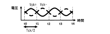
図6のトラック・アンド・ホールド回路の基本的な動作を、図7A~図7Eを用いて説明する。ここでは、図7Aに示す周期Tckの差動クロック信号Vck+,Vck-と、図7Bに示す入力信号Vinとをトラック・アンド・ホールド回路に印加した時の、電流IEE1,IEE2の波形を図7C、図7Dに示し、出力信号Voutの波形を図7Eに示す。図7A~図7Eのt0,t1,t2,t3,t4は時刻を表す。t0~t4は一定間隔Tck/2ごとに並んでいる。
The basic operation of the track-and-hold circuit of FIG. 6 will be described with reference to FIGS. 7A to 7E. Here, the waveforms of the currents IEE1 and IEE2 when the differential clock signals Vck + and Vck− having a period of Tck shown in FIG. 7A and the input signal Vin shown in FIG. 7B are applied to the track and hold circuit are shown in FIG. 7C. , FIG. 7D, and the waveform of the output signal Vout is shown in FIG. 7E. T0, t1, t2, t3, and t4 in FIGS. 7A to 7E represent the time. t0 to t4 are lined up at regular intervals of Tck / 2.
クロック信号がHighのとき、すなわちVck+>Vck-のとき(時刻tがt0≦t≦t1またはt2≦t≦t3を満たすとき)、トランジスタM11がOFF、トランジスタM12がONとなるので、IEE1=IEE、IEE2=0となる。このとき、トランジスタM10のベース-エミッタ間のPN接合がON状態になるため、トランジスタM10のエミッタ電圧(出力信号Vout)は入力信号Vinに追従する。つまり、時刻tがt0≦t≦t1またはt2≦t≦t3を満たすとき、トラック・アンド・ホールド回路はトラックモードとなる。
When the clock signal is High, that is, when Vck +> Vck- (when the time t satisfies t0≤t≤t1 or t2≤t≤t3), the transistor M11 is OFF and the transistor M12 is ON, so IEE1 = IEE. , IEE2 = 0. At this time, since the PN junction between the base and the emitter of the transistor M10 is turned on, the emitter voltage (output signal Vout) of the transistor M10 follows the input signal Vin. That is, when the time t satisfies t0 ≦ t ≦ t1 or t2 ≦ t ≦ t3, the track and hold circuit is in the track mode.
一方、クロック信号がLowのとき、すなわちVck+<Vck-のとき(時刻tがt1≦t≦t2またはt3≦t≦t4を満たすとき)、トランジスタM11がON、トランジスタM12がOFFとなるので、IEE1=0、IEE2=IEEとなる。したがって、トランジスタM10には電流が流れず、トランジスタM10のベース-エミッタ間のPN接合がOFF状態になるため、トランジスタM10のベースとエミッタとが電気的に切り離される。このとき、クロック信号がHighからLowになった瞬間のトランジスタM10のエミッタ電圧(出力信号Vout)がキャパシタCholdに保持されるため、出力信号Voutはクロック信号がLowの間だけ一定値に保持される。つまり、時刻tがt1≦t≦t2またはt3≦t≦t4を満たすとき、トラック・アンド・ホールド回路はホールドモードとなる。
On the other hand, when the clock signal is Low, that is, when Vck + <Vck- (when the time t satisfies t1 ≦ t ≦ t2 or t3 ≦ t ≦ t4), the transistor M11 is turned ON and the transistor M12 is turned OFF. = 0, IEE2 = IEE. Therefore, no current flows through the transistor M10, and the PN junction between the base and the emitter of the transistor M10 is turned off, so that the base and the emitter of the transistor M10 are electrically separated. At this time, since the emitter voltage (output signal Vout) of the transistor M10 at the moment when the clock signal changes from High to Low is held in the capacitor Hold, the output signal Vout is held at a constant value only while the clock signal is Low. .. That is, when the time t satisfies t1 ≦ t ≦ t2 or t3 ≦ t ≦ t4, the track and hold circuit is in the hold mode.
以上、クロック信号のHigh/Lowに応じてトラックモードとホールドモードを交互に繰り返すのがトラック・アンド・ホールド回路の基本的な動作である。
トラック・アンド・ホールド回路のデータレート、すなわち単位時間あたりにデータを取得する回数は、クロック周波数に依存することは明らかである。しかし、アナログ回路の制約条件、具体的にはトランジスタや配線に存在する寄生抵抗、寄生容量等のために、入力できるクロック信号の周波数には上限がある。このクロック信号の周波数の上限が、トラック・アンド・ホールド回路の速度を制限する主要因となる。 As described above, the basic operation of the track-and-hold circuit is to alternately repeat the track mode and the hold mode according to the High / Low of the clock signal.
It is clear that the data rate of the track-and-hold circuit, that is, the number of times data is acquired per unit time, depends on the clock frequency. However, there is an upper limit to the frequency of the clock signal that can be input due to the constraint conditions of the analog circuit, specifically, the parasitic resistance and the parasitic capacitance existing in the transistor and the wiring. The upper limit of the frequency of this clock signal is the main factor that limits the speed of the track-and-hold circuit.
本発明は、上記課題を解決するためになされたもので、トラック・アンド・ホールド回路のデータレートを高速化することを目的とする。
The present invention has been made to solve the above problems, and an object of the present invention is to increase the data rate of a track-and-hold circuit.
本発明のトラック・アンド・ホールド回路は、ベースが信号入力端子に接続され、コレクタに電源電圧が印加され、エミッタが第1の信号出力端子に接続された第1のトランジスタと、ベースが前記信号入力端子に接続され、コレクタに前記電源電圧が印加され、エミッタが第2の信号出力端子に接続された第2のトランジスタと、一端が前記第1のトランジスタのコレクタに接続され、他端が前記第1のトランジスタのエミッタに接続された第1のキャパシタと、一端が前記第2のトランジスタのコレクタに接続され、他端が前記第2のトランジスタのエミッタに接続された第2のキャパシタと、前記第1、第2のトランジスタに定電流を供給するように構成された定電流源と、前記第1、第2のトランジスタのエミッタと前記定電流源との間に接続され、差動クロック信号に応じて前記第1、第2のトランジスタを交互にオン状態にするように構成されたスイッチ回路とを備えることを特徴とするものである。
In the track and hold circuit of the present invention, the base is connected to the signal input terminal, the power supply voltage is applied to the collector, the emitter is connected to the first signal output terminal, and the base is the signal. A second transistor connected to an input terminal, the power supply voltage is applied to a collector, an emitter is connected to a second signal output terminal, one end is connected to the collector of the first transistor, and the other end is said. A first capacitor connected to the emitter of the first transistor, a second capacitor having one end connected to the collector of the second transistor and the other end connected to the emitter of the second transistor, and the above. A constant current source configured to supply a constant current to the first and second transistors is connected between the emitters of the first and second transistors and the constant current source to form a differential clock signal. It is characterized by including a switch circuit configured to alternately turn on the first and second transistors accordingly.
また、本発明のトラック・アンド・ホールド回路の1構成例において、前記スイッチ回路は、ベースが正相クロック入力端子に接続され、コレクタが前記第1のトランジスタのエミッタに接続され、エミッタが前記定電流源に接続された第3のトランジスタと、ベースが逆相クロック入力端子に接続され、コレクタが前記第2のトランジスタのエミッタに接続され、エミッタが前記定電流源に接続された第4のトランジスタとから構成されることを特徴とするものである。
Further, in one configuration example of the track and hold circuit of the present invention, in the switch circuit, the base is connected to the positive phase clock input terminal, the collector is connected to the emitter of the first transistor, and the emitter is the fixed emitter. A third transistor connected to the current source and a fourth transistor whose base is connected to the antiphase clock input terminal, the collector is connected to the emitter of the second transistor, and the emitter is connected to the constant current source. It is characterized by being composed of.
また、本発明のトラック・アンド・ホールド回路は、ベースが正相信号入力端子に接続され、コレクタに電源電圧が印加され、エミッタが第1の正相信号出力端子に接続された第1のトランジスタと、ベースが逆相信号入力端子に接続され、コレクタに前記電源電圧が印加され、エミッタが第1の逆相信号出力端子に接続された第2のトランジスタと、ベースが前記正相信号入力端子に接続され、コレクタに前記電源電圧が印加され、エミッタが第2の正相信号出力端子に接続された第3のトランジスタと、ベースが前記逆相信号入力端子に接続され、コレクタに前記電源電圧が印加され、エミッタが第2の逆相信号出力端子に接続された第4のトランジスタと、一端が前記第1のトランジスタのコレクタに接続され、他端が前記第1のトランジスタのエミッタに接続された第1のキャパシタと、一端が前記第2のトランジスタのコレクタに接続され、他端が前記第2のトランジスタのエミッタに接続された第2のキャパシタと、一端が前記第3のトランジスタのコレクタに接続され、他端が前記第3のトランジスタのエミッタに接続された第3のキャパシタと、一端が前記第4のトランジスタのコレクタに接続され、他端が前記第4のトランジスタのエミッタに接続された第4のキャパシタと、前記第1、第2、第3、第4のトランジスタに定電流を供給するように構成された定電流源と、前記第1、第2、第3、第4のトランジスタのエミッタと前記定電流源との間に接続され、差動クロック信号に応じて前記第1、第2のトランジスタからなる第1の差動回路と前記第3、第4のトランジスタからなる第2の差動回路とを交互にオン状態にするように構成されたスイッチ回路とを備えることを特徴とするものである。
Further, in the track and hold circuit of the present invention, the base is connected to the positive phase signal input terminal, the power supply voltage is applied to the collector, and the emitter is connected to the first positive phase signal output terminal. A second transistor whose base is connected to the negative-phase signal input terminal, the power supply voltage is applied to the collector, and the emitter is connected to the first negative-phase signal output terminal, and the base is the positive-phase signal input terminal. A third transistor connected to the collector, the power supply voltage is applied to the collector, the emitter is connected to the second positive phase signal output terminal, and the base is connected to the negative phase signal input terminal, and the power supply voltage is connected to the collector. Is applied, the emitter is connected to the second anti-phase signal output terminal, the fourth transistor, one end is connected to the collector of the first transistor, and the other end is connected to the emitter of the first transistor. The first capacitor, one end connected to the collector of the second transistor, the other end connected to the emitter of the second transistor, and one end connected to the collector of the third transistor. A third capacitor connected and the other end connected to the emitter of the third transistor, one end connected to the collector of the fourth transistor, and the other end connected to the emitter of the fourth transistor. A fourth capacitor, a constant current source configured to supply a constant current to the first, second, third, and fourth transistors, and the first, second, third, and fourth transistors. A second differential circuit composed of the first and second transistors and a second transistor composed of the third and fourth transistors, which are connected between the emitter and the constant current source and are composed of the first and second transistors according to the differential clock signal. It is characterized by including a switch circuit configured to alternately turn on the differential circuit of the above.
また、本発明のトラック・アンド・ホールド回路の1構成例において、前記スイッチ回路は、ベースが正相クロック入力端子に接続され、コレクタが前記第1のトランジスタのエミッタに接続され、エミッタが前記定電流源に接続された第5のトランジスタと、ベースが前記正相クロック入力端子に接続され、コレクタが前記第2のトランジスタのエミッタに接続され、エミッタが前記定電流源に接続された第6のトランジスタと、ベースが逆相クロック入力端子に接続され、コレクタが前記第3のトランジスタのエミッタに接続され、エミッタが前記定電流源に接続された第7のトランジスタと、ベースが前記逆相クロック入力端子に接続され、コレクタが前記第4のトランジスタのエミッタに接続され、エミッタが前記定電流源に接続された第8のトランジスタとから構成されることを特徴とするものである。
Further, in one configuration example of the track and hold circuit of the present invention, in the switch circuit, the base is connected to the positive phase clock input terminal, the collector is connected to the emitter of the first transistor, and the emitter is the constant. A fifth transistor connected to the current source, a base connected to the positive phase clock input terminal, a collector connected to the emitter of the second transistor, and a sixth transistor connected to the constant current source. A seventh transistor with a transistor and a base connected to the anti-phase clock input terminal, a collector connected to the emitter of the third transistor, an emitter connected to the constant current source, and a base with the anti-phase clock input. It is characterized in that it is connected to a terminal, a collector is connected to the emitter of the fourth transistor, and the emitter is composed of an eighth transistor connected to the constant current source.
本発明によれば、差動クロック信号に応じて第1、第2のトランジスタを交互にオン状態にすることにより、トラックモードになる回路とホールドモードになる回路を差動クロック信号の半周期ごとに替えることができ、従来のトラック・アンド・ホールド回路と比較して2倍のデータレートを実現することができる。
According to the present invention, by alternately turning on the first and second transistors according to the differential clock signal, a circuit that goes into track mode and a circuit that goes into hold mode are switched every half cycle of the differential clock signal. It is possible to realize a data rate twice as high as that of a conventional track-and-hold circuit.
また、本発明では、差動クロック信号に応じて第1、第2のトランジスタからなる第1の差動回路と第3、第4のトランジスタからなる第2の差動回路とを交互にオン状態にすることにより、トラックモードになる差動回路とホールドモードになる差動回路をクロック信号の半周期ごとに替えることができ、従来のトラック・アンド・ホールド回路と比較して2倍のデータレートを実現することができる。
Further, in the present invention, the first differential circuit composed of the first and second transistors and the second differential circuit composed of the third and fourth transistors are alternately turned on according to the differential clock signal. By setting, the differential circuit that goes into track mode and the differential circuit that goes into hold mode can be switched every half cycle of the clock signal, and the data rate is twice that of the conventional track-and-hold circuit. Can be realized.
[第1の実施例]
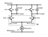
以下、本発明の実施例について図面を参照して説明する。図1は本発明の第1の実施例に係るトラック・アンド・ホールド回路の構成を示す回路図である。図1のVCC,VEEは電源電圧、Vinは入力信号、Voutは出力信号、Vck+,Vck-はクロック信号である。クロック信号Vck+,Vck-は差動信号である。また、図1中の(const.)は電圧または電流が時間によらず一定であることを示している。 [First Example]
Hereinafter, examples of the present invention will be described with reference to the drawings. FIG. 1 is a circuit diagram showing a configuration of a track-and-hold circuit according to a first embodiment of the present invention. In FIG. 1, VCS and VEE are power supply voltages, Vin is an input signal, Vout is an output signal, and Vck + and Vck− are clock signals. The clock signals Vck + and Vck− are differential signals. Further, (const.) In FIG. 1 indicates that the voltage or current is constant regardless of time.
本実施例のトラック・アンド・ホールド回路は、ベースが信号入力端子(Vin)に接続され、コレクタに電源電圧VCCが印加され、エミッタが第1の信号出力端子(Vout1)に接続されたバイポーラトランジスタM1と、ベースが正相クロック入力端子(Vck+)に接続され、コレクタがバイポーラトランジスタM1のエミッタに接続されたバイポーラトランジスタM2と、ベースが信号入力端子(Vin)に接続され、コレクタに電源電圧VCCが印加され、エミッタが第2の信号出力端子(Vout2)に接続されたバイポーラトランジスタM3と、ベースが逆相クロック入力端子(Vck-)に接続され、コレクタがバイポーラトランジスタM3のエミッタに接続されたバイポーラトランジスタM4とを備えている。
In the track-and-hold circuit of this embodiment, the base is connected to the signal input terminal (Vin), the power supply voltage VCS is applied to the collector, and the emitter is connected to the first signal output terminal (Vout1). The M1 and the bipolar transistor M2 whose base is connected to the positive phase clock input terminal (Vck +) and the collector is connected to the emitter of the bipolar transistor M1 and the base are connected to the signal input terminal (Vin), and the power supply voltage VCS is connected to the collector. Was applied, the emitter was connected to the second signal output terminal (Vout2) of the bipolar transistor M3, the base was connected to the antiphase clock input terminal (Vck-), and the collector was connected to the emitter of the bipolar transistor M3. It includes a bipolar transistor M4.
さらに、トラック・アンド・ホールド回路は、一端がバイポーラトランジスタM1のコレクタに接続され、他端がバイポーラトランジスタM1のエミッタに接続されたキャパシタChold1と、一端がバイポーラトランジスタM3のコレクタに接続され、他端がバイポーラトランジスタM3のエミッタに接続されたキャパシタChold2と、一端がバイポーラトランジスタM2,M4のエミッタに接続され、他端が電源電圧VEEに接続された定電流源ISとを備えている。
Further, the track-and-hold circuit has a capacitor Hold1 having one end connected to the collector of the bipolar transistor M1 and the other end connected to the emitter of the bipolar transistor M1 and one end connected to the collector of the bipolar transistor M3. Holds a capacitor Hold2 connected to the emitter of the bipolar transistor M3, and a constant current source IS having one end connected to the emitters of the bipolar transistors M2 and M4 and the other end connected to the power supply voltage VEE.
定電流源ISは、多くの場合トランジスタ等で構成される。IEE1,IEE2は、バイポーラトランジスタM2,M4のエミッタから定電流源ISに流れ込む電流である。定電流源ISに流れる電流をIEEとすると、キルヒホッフの電流則により、IEE1+IEE2=IEEとなる。
トランジスタM2,M4は、差動クロック信号Vck+,Vck-に応じてトランジスタM1,M2を交互にオン状態にするスイッチ回路SW1を構成している。 The constant current source IS is often composed of a transistor or the like. The IEE1 and IEE2 are currents that flow from the emitters of the bipolar transistors M2 and M4 into the constant current source IS. If the current flowing through the constant current source IS is IEE, then according to Kirchhoff's current law, IEE1 + IEE2 = IEE.
The transistors M2 and M4 constitute a switch circuit SW1 that alternately turns on the transistors M1 and M2 according to the differential clock signals Vck + and Vck−.
図1のトラック・アンド・ホールド回路の基本的な動作を、図2A~図2Fを用いて説明する。ここでは、図2Aに示す周期Tckの差動クロック信号Vck+,Vck-と、図2Bに示す入力信号Vinとをトラック・アンド・ホールド回路に印加した時の、電流IEE1,IEE2の波形を図2C、図2Dに示し、出力信号Vout1,Vout2の波形を図2E、図2Fに示す。図2A~図2Fのt0,t1,t2,t3,t4は時刻を表す。t0~t4は一定間隔Tck/2ごとに並んでいる。
The basic operation of the track-and-hold circuit of FIG. 1 will be described with reference to FIGS. 2A to 2F. Here, the waveforms of the currents IEE1 and IEE2 when the differential clock signals Vck + and Vck− having a period Tck shown in FIG. 2A and the input signals Vin shown in FIG. 2B are applied to the track and hold circuit are shown in FIG. 2C. , 2D, and the waveforms of the output signals Vout1 and Vout2 are shown in FIGS. 2E and 2F. T0, t1, t2, t3, and t4 in FIGS. 2A to 2F represent the time. t0 to t4 are lined up at regular intervals of Tck / 2.
クロック信号がHighのとき、すなわちVck+>Vck-のとき(時刻tがt0≦t≦t1またはt2≦t≦t3を満たすとき)、トランジスタM2がON、トランジスタM4がOFFとなるので、IEE1=IEE、IEE2=0となる。このとき、トランジスタM1のベース-エミッタ間のPN接合がON状態になるため、トランジスタM1のエミッタ電圧(出力信号Vout1)は入力信号Vinに追従する。
When the clock signal is High, that is, when Vck +> Vck- (when the time t satisfies t0 ≦ t ≦ t1 or t2 ≦ t ≦ t3), the transistor M2 is turned on and the transistor M4 is turned off, so that IEE1 = IEE. , IEE2 = 0. At this time, since the PN junction between the base and the emitter of the transistor M1 is turned on, the emitter voltage (output signal Vout1) of the transistor M1 follows the input signal Vin.
一方、トランジスタM3,M4には電流が流れないため、トランジスタM3のベース-エミッタ間のPN接合はOFF状態であり、トランジスタM3のベースとエミッタとが電気的に切り離される。このとき、クロック信号がLowからHighになった瞬間のトランジスタM3のエミッタ電圧(出力信号Vout2)がキャパシタChold2に保持されるため、出力信号Vout2はクロック信号がHighの間だけ一定値に保持される。
On the other hand, since no current flows through the transistors M3 and M4, the PN junction between the base and the emitter of the transistor M3 is in the OFF state, and the base and the emitter of the transistor M3 are electrically separated. At this time, since the emitter voltage (output signal Vout2) of the transistor M3 at the moment when the clock signal changes from Low to High is held in the capacitor Hold2, the output signal Vout2 is held at a constant value only while the clock signal is High. ..
このように、クロック信号がHighのとき(時刻tがt0≦t≦t1またはt2≦t≦t3を満たすとき)、トランジスタM1とキャパシタChold1とからなる第1の回路はトラックモードとなり、トランジスタM3とキャパシタChold2とからなる第2の回路はホールドモードとなる。
As described above, when the clock signal is High (when the time t satisfies t0 ≦ t ≦ t1 or t2 ≦ t ≦ t3), the first circuit including the transistor M1 and the capacitor Hold1 is in the track mode, and the transistor M3 The second circuit including the capacitor Clock2 is in the hold mode.
反対に、クロックがLowのとき、すなわちVck+<Vck-のとき(時刻tがt1≦t≦t2またはt3≦t≦t4を満たすとき)、トランジスタM2がOFF、トランジスタM4がONとなるので、IEE1=0、IEE2=IEEとなる。このとき、トランジスタM1とキャパシタChold1とからなる第1の回路はホールドモードとなり、トランジスタM3とキャパシタChold2とからなる第2の回路はトラックモードとなる。
On the contrary, when the clock is Low, that is, when Vck + <Vck- (when the time t satisfies t1 ≦ t ≦ t2 or t3 ≦ t ≦ t4), the transistor M2 is turned off and the transistor M4 is turned on. = 0, IEE2 = IEE. At this time, the first circuit including the transistor M1 and the capacitor Hold1 is in the hold mode, and the second circuit including the transistor M3 and the capacitor Hold2 is in the track mode.
つまり、本実施例では、第1の回路と第2の回路とを相補的に動作させることにより、トラックモードになる回路とホールドモードになる回路をクロック信号の半周期Tck/2ごとに替えることができる。
That is, in this embodiment, by operating the first circuit and the second circuit in a complementary manner, the circuit in the track mode and the circuit in the hold mode are replaced every half cycle Tck / 2 of the clock signal. Can be done.
本実施例においてもトランジスタや配線に存在する寄生抵抗、寄生容量は従来型の回路構成と同様であるため、入力できるクロック周波数の上限は従来と同様となる。ただし、上記のとおりトラックモードになる回路とホールドモードになる回路がクロック信号の半周期Tck/2ごとに替わるので、図6に示した従来の回路構成と比べると、同じ周波数のクロック信号を用いる従来と同条件にもかかわらず、半分の時間間隔で入力信号を取得することができるので、データレートを2倍にすることができる。したがって、本実施例によれば、トラック・アンド・ホールド回路の高速化を実現することができる。
Also in this embodiment, the parasitic resistance and parasitic capacitance existing in the transistor and wiring are the same as in the conventional circuit configuration, so the upper limit of the input clock frequency is the same as in the conventional one. However, as described above, the circuit that enters the track mode and the circuit that enters the hold mode change every half cycle Tck / 2 of the clock signal, so that a clock signal having the same frequency is used as compared with the conventional circuit configuration shown in FIG. Despite the same conditions as before, the input signal can be acquired at half the time interval, so the data rate can be doubled. Therefore, according to this embodiment, the speed of the track-and-hold circuit can be increased.
なお、本実施例のトラック・アンド・ホールド回路を後段のADCと接続する場合、出力信号Vout1を入力とするADCと、出力端子Vout2を入力とするADCを別個に設け、2個のADCから出力されるデジタル信号を合成すればよい。
また、本実施例のトラック・アンド・ホールド回路と1個のADCとの間にマルチプレクサを設け、出力信号Vout1,Vout2のうちクロック信号に同期してホールドモード状態にある方の出力信号を常に選択してADCに出力するようにマルチプレクサを切り替えるようにしてもよい。 When the track-and-hold circuit of this embodiment is connected to the ADC in the subsequent stage, an ADC that inputs the output signal Vout1 and an ADC that inputs the output terminal Vout2 are separately provided and output from the two ADCs. The digital signals to be generated may be synthesized.
Further, a multiplexer is provided between the track and hold circuit of this embodiment and one ADC, and the output signal of the output signals Vout1 and Vout2, which is in the hold mode state in synchronization with the clock signal, is always selected. Then, the multiplexer may be switched so as to output to the ADC.
[第2の実施例]
次に、本発明の第2の実施例について説明する。図3は本発明の第2の実施例に係るトラック・アンド・ホールド回路の構成を示す回路図である。本実施例のトラック・アンド・ホールド回路は、ベースが正相信号入力端子(Vin+)に接続され、コレクタに電源電圧VCCが印加され、エミッタが第1の正相信号出力端子(Vout1+)に接続されたバイポーラトランジスタM1と、ベースが正相クロック入力端子(Vck+)に接続され、コレクタがバイポーラトランジスタM1のエミッタに接続されたバイポーラトランジスタM2と、ベースが正相信号入力端子(Vin+)に接続され、コレクタに電源電圧VCCが印加され、エミッタが第2の正相信号出力端子(Vout2+)に接続されたバイポーラトランジスタM3と、ベースが逆相クロック入力端子(Vck-)に接続され、コレクタがバイポーラトランジスタM3のエミッタに接続されたバイポーラトランジスタM4と、ベースが逆相信号入力端子(Vin-)に接続され、コレクタに電源電圧VCCが印加され、エミッタが第1の逆相信号出力端子(Vout1-)に接続されたバイポーラトランジスタM5と、ベースが正相クロック入力端子(Vck+)に接続され、コレクタがバイポーラトランジスタM5のエミッタに接続されたバイポーラトランジスタM6と、ベースが逆相信号入力端子(Vin-)に接続され、コレクタに電源電圧VCCが印加され、エミッタが第2の逆相信号出力端子(Vout2-)に接続されたバイポーラトランジスタM7と、ベースが逆相クロック入力端子(Vck-)に接続され、コレクタがバイポーラトランジスタM7のエミッタに接続されたバイポーラトランジスタM8とを備えている。 [Second Example]
Next, a second embodiment of the present invention will be described. FIG. 3 is a circuit diagram showing a configuration of a track-and-hold circuit according to a second embodiment of the present invention. In the track-and-hold circuit of this embodiment, the base is connected to the positive-phase signal input terminal (Vin +), the power supply voltage VCS is applied to the collector, and the emitter is connected to the first positive-phase signal output terminal (Vout1 +). The bipolar transistor M1 and the base are connected to the positive phase clock input terminal (Vck +), the collector is connected to the emitter of the bipolar transistor M1, the bipolar transistor M2, and the base is connected to the positive phase signal input terminal (Vin +). , The power supply voltage VCS is applied to the collector, the emitter is connected to the second positive phase signal output terminal (Vout2 +), the bipolar transistor M3, and the base is connected to the reverse phase clock input terminal (Vck-), and the collector is bipolar. The bipolar transistor M4 connected to the emitter of the transistor M3 and the base are connected to the anti-phase signal input terminal (Vin-), the power supply voltage VCS is applied to the collector, and the emitter is the first anti-phase signal output terminal (Vout1-). ), The bipolar transistor M6 whose base is connected to the positive phase clock input terminal (Vck +) and the collector connected to the emitter of the bipolar transistor M5, and the base is the negative phase signal input terminal (Vin-). ), The power supply voltage VCS is applied to the collector, the emitter is connected to the second anti-phase signal output terminal (Vout2-), and the base is connected to the anti-phase clock input terminal (Vck-). The collector is provided with a bipolar transistor M8 connected to the emitter of the bipolar transistor M7.
さらに、トラック・アンド・ホールド回路は、一端がバイポーラトランジスタM1のコレクタに接続され、他端がバイポーラトランジスタM1のエミッタに接続されたキャパシタChold1と、一端がバイポーラトランジスタM3のコレクタに接続され、他端がバイポーラトランジスタM3のエミッタに接続されたキャパシタChold2と、一端がバイポーラトランジスタM5のコレクタに接続され、他端がバイポーラトランジスタM5のエミッタに接続されたキャパシタChold3と、一端がバイポーラトランジスタM7のコレクタに接続され、他端がバイポーラトランジスタM7のエミッタに接続されたキャパシタChold4と、一端がバイポーラトランジスタM2,M4,M6,M8のエミッタに接続され、他端が電源電圧VEEに接続された定電流源ISとを備えている。
Further, the track-and-hold circuit has a capacitor Hold1 having one end connected to the collector of the bipolar transistor M1 and the other end connected to the emitter of the bipolar transistor M1 and one end connected to the collector of the bipolar transistor M3. Is connected to the capacitor Hold2 connected to the emitter of the bipolar transistor M3, one end is connected to the collector of the bipolar transistor M5, the other end is connected to the capacitor Hold3 connected to the emitter of the bipolar transistor M5, and one end is connected to the collector of the bipolar transistor M7. The other end is connected to the emitter of the bipolar transistor M7, and the other end is connected to the emitter of the bipolar transistors M2, M4, M6, M8, and the other end is connected to the power supply voltage VEE. It has.
トランジスタM2,M4,M6,M8は、差動クロック信号Vck+,Vck-に応じてトランジスタM1,M5からなる第1の差動回路とトランジスタM3,M7からなる第2の差動回路とを交互にオン状態にするスイッチ回路SW2を構成している。
The transistors M2, M4, M6, and M8 alternately alternate between a first differential circuit composed of transistors M1 and M5 and a second differential circuit composed of transistors M3 and M7 according to the differential clock signals Vck + and Vck−. The switch circuit SW2 for turning on is configured.
図3のトラック・アンド・ホールド回路の基本的な動作を、図4A~図4Fを用いて説明する。ここでは、図4に示す周期Tckの差動クロック信号Vck+,Vck-と、図4B、図4Cに示す差動入力信号Vin+,Vin-とをトラック・アンド・ホールド回路に印加した時の、差動出力信号Vout1+,Vout1-の波形を図4D、図4Eに示し、差動出力信号Vout2+,Vout2-の波形を図4F、図4Gに示す。
The basic operation of the track-and-hold circuit of FIG. 3 will be described with reference to FIGS. 4A to 4F. Here, the difference between the differential clock signals Vck + and Vck− having a period of Tck shown in FIG. 4 and the differential input signals Vin + and Vin− shown in FIGS. 4B and 4C when applied to the track and hold circuit. The waveforms of the dynamic output signals Vout1 + and Vout1- are shown in FIGS. 4D and 4E, and the waveforms of the differential output signals Vout2 + and Vout2- are shown in FIGS. 4F and 4G.
クロック信号がHighのとき、すなわちVck+>Vck-のとき(時刻tがt0≦t≦t1またはt2≦t≦t3を満たすとき)、トランジスタM2,M6がON、トランジスタM4,M8がOFFとなり、トランジスタM1,M5のベース-エミッタ間のPN接合がON状態になるため、トランジスタM1のエミッタ電圧(出力信号Vout1+)は入力信号Vin+に追従し、トランジスタM5のエミッタ電圧(出力信号Vout1-)は入力信号Vin-に追従する。
When the clock signal is High, that is, when Vck +> Vck- (when the time t satisfies t0 ≦ t ≦ t1 or t2 ≦ t ≦ t3), the transistors M2 and M6 are turned on, the transistors M4 and M8 are turned off, and the transistors are turned off. Since the PN junction between the base and the emitter of M1 and M5 is turned on, the emitter voltage of the transistor M1 (output signal Vout1 +) follows the input signal Vin +, and the emitter voltage of the transistor M5 (output signal Vout1-) is the input signal. Follow Vin-.
一方、トランジスタM3,M4,M7,M8には電流が流れないため、トランジスタM3,M7のベース-エミッタ間のPN接合はOFF状態であり、トランジスタM3,M7のベースとエミッタとが電気的に切り離される。このとき、クロック信号がLowからHighになった瞬間のトランジスタM3のエミッタ電圧(出力信号Vout2+)がキャパシタChold2に保持されるため、出力信号Vout2+はクロック信号がHighの間だけ一定値に保持される。同様に、クロック信号がLowからHighになった瞬間のトランジスタM7のエミッタ電圧(出力信号Vout2-)がキャパシタChold4に保持されるため、出力信号Vout2-はクロック信号がHighの間だけ一定値に保持される。
On the other hand, since no current flows through the transistors M3, M4, M7, and M8, the PN junction between the base and the emitter of the transistors M3 and M7 is in the OFF state, and the base and the emitter of the transistors M3 and M7 are electrically separated. Is done. At this time, since the emitter voltage (output signal Vout2 +) of the transistor M3 at the moment when the clock signal changes from Low to High is held in the capacitor Hold2, the output signal Vout2 + is held at a constant value only while the clock signal is High. .. Similarly, since the emitter voltage (output signal Vout2-) of the transistor M7 at the moment when the clock signal changes from Low to High is held in the capacitor Hold4, the output signal Vout2- is held at a constant value only while the clock signal is High. Will be done.
このように、クロック信号がHighのとき(時刻tがt0≦t≦t1またはt2≦t≦t3を満たすとき)、トランジスタM1,M5とキャパシタChold1,Chold3とからなる第1の差動回路はトラックモードとなり、トランジスタM3,M7とキャパシタChold2,Chold4とからなる第2の差動回路はホールドモードとなる。
As described above, when the clock signal is High (when the time t satisfies t0 ≦ t ≦ t1 or t2 ≦ t ≦ t3), the first differential circuit including the transistors M1 and M5 and the capacitors Hold1 and Hold3 is a track. The mode is set, and the second differential circuit including the transistors M3 and M7 and the capacitors Hold2 and Hold4 is in the hold mode.
反対に、クロックがLowのとき、すなわちVck+<Vck-のとき(時刻tがt1≦t≦t2またはt3≦t≦t4を満たすとき)、トランジスタM2,M6がOFF、トランジスタM4,M8がONとなる。このとき、トランジスタM1,M5とキャパシタChold1,Chold3とからなる第1の差動回路はホールドモードとなり、トランジスタM3,M7とキャパシタChold2,Chold4とからなる第2の差動回路はトラックモードとなる。
On the contrary, when the clock is Low, that is, when Vck + <Vck- (when the time t satisfies t1 ≦ t ≦ t2 or t3 ≦ t ≦ t4), the transistors M2 and M6 are OFF, and the transistors M4 and M8 are ON. Become. At this time, the first differential circuit including the transistors M1 and M5 and the capacitors Hold1 and Hold3 is in the hold mode, and the second differential circuit including the transistors M3 and M7 and the capacitors Hold2 and Hold4 is in the track mode.
つまり、本実施例では、第1の差動回路と第2の差動回路とを相補的に動作させることにより、トラックモードになる差動回路とホールドモードになる差動回路をクロック信号の半周期Tck/2ごとに替えることができる。
That is, in this embodiment, by operating the first differential circuit and the second differential circuit in a complementary manner, the differential circuit in the track mode and the differential circuit in the hold mode are half of the clock signal. It can be changed every 2 cycles Tck / 2.
このように、本実施例では、クロック入力のトランジスタだけでなく信号入力のトランジスタも差動構成とすることにより、同相ノイズの除去や非線形歪みの除去が可能になる。また、図3のように定電流源ISを一本化することで回路規模の小面積化を実現することができる。
As described above, in this embodiment, by forming not only the clock input transistor but also the signal input transistor in a differential configuration, it is possible to remove in-phase noise and non-linear distortion. Further, by unifying the constant current source IS as shown in FIG. 3, it is possible to realize a small circuit area.
なお、トラック・アンド・ホールド回路と後段のADCとの接続形態は第1の実施例と同様である。2個のADCを用いる場合には、差動出力信号Vout1+,Vout1-を入力とする差動入力型のADCと、差動出力信号Vout2+,Vout2-を入力とする差動入力型のADCとを設けるようにすればよい。
The connection form between the track and hold circuit and the ADC in the subsequent stage is the same as in the first embodiment. When two ADCs are used, a differential input type ADC that inputs the differential output signals Vout1 + and Vout1- and a differential input type ADC that inputs the differential output signals Vout2 + and Vout2- are used. It may be provided.
マルチプレクサを用いる場合には、差動出力信号Vout1+,Vout1-と差動出力信号Vout2+,Vout2-のうちホールドモード状態にある方の差動出力信号を選択して出力する差動入力差動出力型のマルチプレクサと、マルチプレクサの差動出力信号を入力とする差動入力型のADCとを設けるようにすればよい。あるいは、差動出力信号Vout1+,Vout1-と差動出力信号Vout2+,Vout2-のうちホールドモード状態にある方の差動出力信号を単相信号に変換して出力する差動入力単相出力型のマルチプレクサと、マルチプレクサの出力信号を入力とする単相入力型のADCとを設けるようにすればよい。
When using a multiplexer, a differential input differential output type that selects and outputs the differential output signal Vout1 +, Vout1- and the differential output signals Vout2 +, Vout2-, whichever is in the hold mode state. The multiplexer and the differential input type ADC that receives the differential output signal of the multiplexer as input may be provided. Alternatively, a differential input single-phase output type that converts the differential output signal of the differential output signals Vout1 +, Vout1- and the differential output signals Vout2 +, Vout2-, which is in the hold mode state, into a single-phase signal and outputs the signal. A multiplexer and a single-phase input type ADC that receives the output signal of the multiplexer as an input may be provided.
以上に示した実施例はあくまで本発明の原理の理解の補助となるよう応用の一事例を示しているに過ぎず、実際の状況における実施例には、本発明の思想を逸脱しない範囲内で多くの変形が認められる。
The examples shown above are merely examples of applications so as to assist in understanding the principle of the present invention, and the examples in actual situations are provided within the range not departing from the idea of the present invention. Many deformations are observed.
本発明は、トラック・アンド・ホールド回路に適用することができる。
The present invention can be applied to a track and hold circuit.
M1~M8…バイポーラトランジスタ、Chold1~Chold4…キャパシタ、IS…定電流源、SW1,SW2…スイッチ回路。
M1 to M8 ... Bipolar transistor, Hold1 to Hold4 ... Capacitor, IS ... Constant current source, SW1, SW2 ... Switch circuit.
Claims (4)
- ベースが信号入力端子に接続され、コレクタに電源電圧が印加され、エミッタが第1の信号出力端子に接続された第1のトランジスタと、
ベースが前記信号入力端子に接続され、コレクタに前記電源電圧が印加され、エミッタが第2の信号出力端子に接続された第2のトランジスタと、
一端が前記第1のトランジスタのコレクタに接続され、他端が前記第1のトランジスタのエミッタに接続された第1のキャパシタと、
一端が前記第2のトランジスタのコレクタに接続され、他端が前記第2のトランジスタのエミッタに接続された第2のキャパシタと、
前記第1、第2のトランジスタに定電流を供給するように構成された定電流源と、
前記第1、第2のトランジスタのエミッタと前記定電流源との間に接続され、差動クロック信号に応じて前記第1、第2のトランジスタを交互にオン状態にするように構成されたスイッチ回路とを備えることを特徴とするトラック・アンド・ホールド回路。 A first transistor whose base is connected to the signal input terminal, a power supply voltage is applied to the collector, and the emitter is connected to the first signal output terminal.
A second transistor whose base is connected to the signal input terminal, the power supply voltage is applied to the collector, and the emitter is connected to the second signal output terminal.
A first capacitor having one end connected to the collector of the first transistor and the other end connected to the emitter of the first transistor.
A second capacitor, one end connected to the collector of the second transistor and the other end connected to the emitter of the second transistor.
A constant current source configured to supply a constant current to the first and second transistors, and
A switch connected between the emitters of the first and second transistors and the constant current source, and configured to alternately turn on the first and second transistors according to a differential clock signal. A track-and-hold circuit characterized by having a circuit. - 請求項1記載のトラック・アンド・ホールド回路において、
前記スイッチ回路は、
ベースが正相クロック入力端子に接続され、コレクタが前記第1のトランジスタのエミッタに接続され、エミッタが前記定電流源に接続された第3のトランジスタと、
ベースが逆相クロック入力端子に接続され、コレクタが前記第2のトランジスタのエミッタに接続され、エミッタが前記定電流源に接続された第4のトランジスタとから構成されることを特徴とするトラック・アンド・ホールド回路。 In the track and hold circuit according to claim 1,
The switch circuit
A third transistor whose base is connected to the positive phase clock input terminal, whose collector is connected to the emitter of the first transistor, and whose emitter is connected to the constant current source.
A track characterized in that a base is connected to an antiphase clock input terminal, a collector is connected to the emitter of the second transistor, and the emitter is composed of a fourth transistor connected to the constant current source. And hold circuit. - ベースが正相信号入力端子に接続され、コレクタに電源電圧が印加され、エミッタが第1の正相信号出力端子に接続された第1のトランジスタと、
ベースが逆相信号入力端子に接続され、コレクタに前記電源電圧が印加され、エミッタが第1の逆相信号出力端子に接続された第2のトランジスタと、
ベースが前記正相信号入力端子に接続され、コレクタに前記電源電圧が印加され、エミッタが第2の正相信号出力端子に接続された第3のトランジスタと、
ベースが前記逆相信号入力端子に接続され、コレクタに前記電源電圧が印加され、エミッタが第2の逆相信号出力端子に接続された第4のトランジスタと、
一端が前記第1のトランジスタのコレクタに接続され、他端が前記第1のトランジスタのエミッタに接続された第1のキャパシタと、
一端が前記第2のトランジスタのコレクタに接続され、他端が前記第2のトランジスタのエミッタに接続された第2のキャパシタと、
一端が前記第3のトランジスタのコレクタに接続され、他端が前記第3のトランジスタのエミッタに接続された第3のキャパシタと、
一端が前記第4のトランジスタのコレクタに接続され、他端が前記第4のトランジスタのエミッタに接続された第4のキャパシタと、
前記第1、第2、第3、第4のトランジスタに定電流を供給するように構成された定電流源と、
前記第1、第2、第3、第4のトランジスタのエミッタと前記定電流源との間に接続され、差動クロック信号に応じて前記第1、第2のトランジスタからなる第1の差動回路と前記第3、第4のトランジスタからなる第2の差動回路とを交互にオン状態にするように構成されたスイッチ回路とを備えることを特徴とするトラック・アンド・ホールド回路。 A first transistor whose base is connected to the positive phase signal input terminal, a power supply voltage is applied to the collector, and the emitter is connected to the first positive phase signal output terminal.
A second transistor whose base is connected to the negative phase signal input terminal, the power supply voltage is applied to the collector, and the emitter is connected to the first negative phase signal output terminal.
A third transistor whose base is connected to the positive phase signal input terminal, the power supply voltage is applied to the collector, and the emitter is connected to the second positive phase signal output terminal.
A fourth transistor whose base is connected to the negative phase signal input terminal, the power supply voltage is applied to the collector, and the emitter is connected to the second negative phase signal output terminal.
A first capacitor having one end connected to the collector of the first transistor and the other end connected to the emitter of the first transistor.
A second capacitor, one end connected to the collector of the second transistor and the other end connected to the emitter of the second transistor.
A third capacitor, one end connected to the collector of the third transistor and the other end connected to the emitter of the third transistor.
A fourth capacitor, one end connected to the collector of the fourth transistor and the other end connected to the emitter of the fourth transistor.
A constant current source configured to supply a constant current to the first, second, third, and fourth transistors, and a constant current source.
A first differential that is connected between the emitters of the first, second, third, and fourth transistors and the constant current source, and is composed of the first and second transistors according to a differential clock signal. A track-and-hold circuit comprising: a switch circuit configured to alternately turn on a circuit and a second differential circuit composed of the third and fourth transistors. - 請求項3記載のトラック・アンド・ホールド回路において、
前記スイッチ回路は、
ベースが正相クロック入力端子に接続され、コレクタが前記第1のトランジスタのエミッタに接続され、エミッタが前記定電流源に接続された第5のトランジスタと、
ベースが前記正相クロック入力端子に接続され、コレクタが前記第2のトランジスタのエミッタに接続され、エミッタが前記定電流源に接続された第6のトランジスタと、
ベースが逆相クロック入力端子に接続され、コレクタが前記第3のトランジスタのエミッタに接続され、エミッタが前記定電流源に接続された第7のトランジスタと、
ベースが前記逆相クロック入力端子に接続され、コレクタが前記第4のトランジスタのエミッタに接続され、エミッタが前記定電流源に接続された第8のトランジスタとから構成されることを特徴とするトラック・アンド・ホールド回路。 In the track and hold circuit according to claim 3,
The switch circuit
A fifth transistor with a base connected to the positive phase clock input terminal, a collector connected to the emitter of the first transistor, and an emitter connected to the constant current source.
A sixth transistor in which the base is connected to the positive phase clock input terminal, the collector is connected to the emitter of the second transistor, and the emitter is connected to the constant current source.
A seventh transistor with a base connected to the anti-phase clock input terminal, a collector connected to the emitter of the third transistor, and an emitter connected to the constant current source.
A track characterized in that a base is connected to the reversed-phase clock input terminal, a collector is connected to the emitter of the fourth transistor, and the emitter is composed of an eighth transistor connected to the constant current source. -And-hold circuit.
Priority Applications (3)
| Application Number | Priority Date | Filing Date | Title |
|---|---|---|---|
| JP2021573658A JP7331956B2 (en) | 2020-01-28 | 2020-01-28 | Track and hold circuit |
| PCT/JP2020/002895 WO2021152687A1 (en) | 2020-01-28 | 2020-01-28 | Track and hold circuit |
| US17/793,628 US11830560B2 (en) | 2020-01-28 | 2020-01-28 | Track-and-hold circuit |
Applications Claiming Priority (1)
| Application Number | Priority Date | Filing Date | Title |
|---|---|---|---|
| PCT/JP2020/002895 WO2021152687A1 (en) | 2020-01-28 | 2020-01-28 | Track and hold circuit |
Publications (1)
| Publication Number | Publication Date |
|---|---|
| WO2021152687A1 true WO2021152687A1 (en) | 2021-08-05 |
Family
ID=77078050
Family Applications (1)
| Application Number | Title | Priority Date | Filing Date |
|---|---|---|---|
| PCT/JP2020/002895 WO2021152687A1 (en) | 2020-01-28 | 2020-01-28 | Track and hold circuit |
Country Status (3)
| Country | Link |
|---|---|
| US (1) | US11830560B2 (en) |
| JP (1) | JP7331956B2 (en) |
| WO (1) | WO2021152687A1 (en) |
Families Citing this family (1)
| Publication number | Priority date | Publication date | Assignee | Title |
|---|---|---|---|---|
| WO2021205592A1 (en) * | 2020-04-09 | 2021-10-14 | 日本電信電話株式会社 | Switched emitter follower circuit |
Citations (5)
| Publication number | Priority date | Publication date | Assignee | Title |
|---|---|---|---|---|
| JPH0729391A (en) * | 1993-07-08 | 1995-01-31 | Fujitsu Ltd | Sample-and-hold circuit |
| JPH1092190A (en) * | 1996-06-21 | 1998-04-10 | General Motors Corp <Gm> | Tracking and holding circuit |
| JP2009230842A (en) * | 2008-02-27 | 2009-10-08 | Yokogawa Electric Corp | Sample-hold circuit |
| JP2017153021A (en) * | 2016-02-26 | 2017-08-31 | 日本電信電話株式会社 | Track-and-hold circuit |
| WO2019172171A1 (en) * | 2018-03-08 | 2019-09-12 | 日本電信電話株式会社 | Track-and-hold circuit |
Family Cites Families (2)
| Publication number | Priority date | Publication date | Assignee | Title |
|---|---|---|---|---|
| US6028459A (en) * | 1998-04-20 | 2000-02-22 | National Semiconductor Corporation | Track and hold circuit with clamp |
| JP4247181B2 (en) * | 2004-11-30 | 2009-04-02 | 富士通株式会社 | Sample hold circuit |
-
2020
- 2020-01-28 JP JP2021573658A patent/JP7331956B2/en active Active
- 2020-01-28 US US17/793,628 patent/US11830560B2/en active Active
- 2020-01-28 WO PCT/JP2020/002895 patent/WO2021152687A1/en active Application Filing
Patent Citations (5)
| Publication number | Priority date | Publication date | Assignee | Title |
|---|---|---|---|---|
| JPH0729391A (en) * | 1993-07-08 | 1995-01-31 | Fujitsu Ltd | Sample-and-hold circuit |
| JPH1092190A (en) * | 1996-06-21 | 1998-04-10 | General Motors Corp <Gm> | Tracking and holding circuit |
| JP2009230842A (en) * | 2008-02-27 | 2009-10-08 | Yokogawa Electric Corp | Sample-hold circuit |
| JP2017153021A (en) * | 2016-02-26 | 2017-08-31 | 日本電信電話株式会社 | Track-and-hold circuit |
| WO2019172171A1 (en) * | 2018-03-08 | 2019-09-12 | 日本電信電話株式会社 | Track-and-hold circuit |
Also Published As
| Publication number | Publication date |
|---|---|
| JPWO2021152687A1 (en) | 2021-08-05 |
| US11830560B2 (en) | 2023-11-28 |
| US20230048012A1 (en) | 2023-02-16 |
| JP7331956B2 (en) | 2023-08-23 |
Similar Documents
| Publication | Publication Date | Title |
|---|---|---|
| VorenKamp et al. | A 12-b, 60-MSample/s cascaded folding and interpolating ADC | |
| US8089388B2 (en) | Folding analog-to-digital converter | |
| US7782096B2 (en) | Track-and-hold circuit with low distortion | |
| US20100103015A1 (en) | Differential amplifier circuit amplifying differential signals with selectively switching between differential signals and ad converter apparatus | |
| US11095300B2 (en) | Reduced noise dynamic comparator for a successive approximation register analog-to-digital converter | |
| US7403149B2 (en) | Folding and interpolating analog-to-digital converter and method of converting analog signal to digital signal | |
| WO2021152687A1 (en) | Track and hold circuit | |
| EP2051382B1 (en) | Folding circuit and analog-to-digital converter | |
| JP2004312555A (en) | Comparator, differential amplifier, two-stage amplifier, and analog/digital converter | |
| US6859158B2 (en) | Analog-digital conversion circuit | |
| WO2009009420A2 (en) | Low glitch offset correction circuit for auto-zero sensor amplifiers and method | |
| US20120286986A1 (en) | A/d conversion circuit | |
| US7098829B2 (en) | Digital to analog conversion | |
| US7804337B2 (en) | Method and apparatus of SFDR enhancement | |
| US8941414B2 (en) | Track-and-hold circuit with low distortion | |
| JPH05191238A (en) | Pwm circuit | |
| JPS59104827A (en) | Integrated circuit for analog-digital conversion | |
| JP5768072B2 (en) | D / A converter and delta-sigma type D / A converter | |
| WO2021205592A1 (en) | Switched emitter follower circuit | |
| JP7444244B2 (en) | track and hold circuit | |
| EP1271781B1 (en) | Comparator circuit | |
| US10523231B1 (en) | Dynamic integrator with boosted output impedance of the transconductance | |
| Boni et al. | 3.3-V, 200-Ms/s BiCMOS comparator for current-mode interpolation using a transconductance stage | |
| Cui et al. | Low power 10-b 250 Msample/s CMOS cascaded folding and interpolating A/D converter | |
| JPH09307442A (en) | Comparator |
Legal Events
| Date | Code | Title | Description |
|---|---|---|---|
| 121 | Ep: the epo has been informed by wipo that ep was designated in this application |
Ref document number: 20916844 Country of ref document: EP Kind code of ref document: A1 |
|
| ENP | Entry into the national phase |
Ref document number: 2021573658 Country of ref document: JP Kind code of ref document: A |
|
| NENP | Non-entry into the national phase |
Ref country code: DE |
|
| 122 | Ep: pct application non-entry in european phase |
Ref document number: 20916844 Country of ref document: EP Kind code of ref document: A1 |