WO2021140998A1 - 半導体装置、および半導体装置システム - Google Patents
半導体装置、および半導体装置システム Download PDFInfo
- Publication number
- WO2021140998A1 WO2021140998A1 PCT/JP2020/049287 JP2020049287W WO2021140998A1 WO 2021140998 A1 WO2021140998 A1 WO 2021140998A1 JP 2020049287 W JP2020049287 W JP 2020049287W WO 2021140998 A1 WO2021140998 A1 WO 2021140998A1
- Authority
- WO
- WIPO (PCT)
- Prior art keywords
- clock signal
- terminal
- semiconductor device
- unit
- frequency
- Prior art date
- Legal status (The legal status is an assumption and is not a legal conclusion. Google has not performed a legal analysis and makes no representation as to the accuracy of the status listed.)
- Ceased
Links
Images






Classifications
-
- H—ELECTRICITY
- H05—ELECTRIC TECHNIQUES NOT OTHERWISE PROVIDED FOR
- H05B—ELECTRIC HEATING; ELECTRIC LIGHT SOURCES NOT OTHERWISE PROVIDED FOR; CIRCUIT ARRANGEMENTS FOR ELECTRIC LIGHT SOURCES, IN GENERAL
- H05B45/00—Circuit arrangements for operating light-emitting diodes [LED]
- H05B45/30—Driver circuits
- H05B45/37—Converter circuits
- H05B45/3725—Switched mode power supply [SMPS]
- H05B45/375—Switched mode power supply [SMPS] using buck topology
-
- G—PHYSICS
- G06—COMPUTING OR CALCULATING; COUNTING
- G06F—ELECTRIC DIGITAL DATA PROCESSING
- G06F1/00—Details not covered by groups G06F3/00 - G06F13/00 and G06F21/00
- G06F1/04—Generating or distributing clock signals or signals derived directly therefrom
- G06F1/08—Clock generators with changeable or programmable clock frequency
-
- G—PHYSICS
- G06—COMPUTING OR CALCULATING; COUNTING
- G06F—ELECTRIC DIGITAL DATA PROCESSING
- G06F1/00—Details not covered by groups G06F3/00 - G06F13/00 and G06F21/00
- G06F1/04—Generating or distributing clock signals or signals derived directly therefrom
- G06F1/12—Synchronisation of different clock signals provided by a plurality of clock generators
-
- G—PHYSICS
- G06—COMPUTING OR CALCULATING; COUNTING
- G06F—ELECTRIC DIGITAL DATA PROCESSING
- G06F1/00—Details not covered by groups G06F3/00 - G06F13/00 and G06F21/00
- G06F1/26—Power supply means, e.g. regulation thereof
- G06F1/28—Supervision thereof, e.g. detecting power-supply failure by out of limits supervision
-
- G—PHYSICS
- G06—COMPUTING OR CALCULATING; COUNTING
- G06F—ELECTRIC DIGITAL DATA PROCESSING
- G06F13/00—Interconnection of, or transfer of information or other signals between, memories, input/output devices or central processing units
- G06F13/38—Information transfer, e.g. on bus
- G06F13/40—Bus structure
- G06F13/4004—Coupling between buses
- G06F13/4022—Coupling between buses using switching circuits, e.g. switching matrix, connection or expansion network
-
- H—ELECTRICITY
- H05—ELECTRIC TECHNIQUES NOT OTHERWISE PROVIDED FOR
- H05B—ELECTRIC HEATING; ELECTRIC LIGHT SOURCES NOT OTHERWISE PROVIDED FOR; CIRCUIT ARRANGEMENTS FOR ELECTRIC LIGHT SOURCES, IN GENERAL
- H05B45/00—Circuit arrangements for operating light-emitting diodes [LED]
- H05B45/30—Driver circuits
- H05B45/32—Pulse-control circuits
- H05B45/325—Pulse-width modulation [PWM]
-
- H—ELECTRICITY
- H05—ELECTRIC TECHNIQUES NOT OTHERWISE PROVIDED FOR
- H05B—ELECTRIC HEATING; ELECTRIC LIGHT SOURCES NOT OTHERWISE PROVIDED FOR; CIRCUIT ARRANGEMENTS FOR ELECTRIC LIGHT SOURCES, IN GENERAL
- H05B45/00—Circuit arrangements for operating light-emitting diodes [LED]
- H05B45/50—Circuit arrangements for operating light-emitting diodes [LED] responsive to malfunctions or undesirable behaviour of LEDs; responsive to LED life; Protective circuits
Definitions
- the present invention relates to a semiconductor device having an oscillator.
- a semiconductor device formed including a semiconductor integrated circuit is often provided with an oscillator that generates a clock signal.
- a PWM (Pulse Width Modulation) signal can be generated based on a clock signal.
- the semiconductor device is, for example, an LED (Light Emitting Diode) drive device (LED driver)
- LED driver Light Emitting Diode
- An example of an LED drive device having a PWM dimming function is disclosed in Patent Document 1.
- a system may be configured by using a plurality of the above semiconductor devices.
- the frequency of the clock signal generated by the oscillator included in each semiconductor device varies. If the frequency of the clock signal varies, for example, the PWM signal may not be synchronized. In this case, for example, there is a possibility that a defect may occur in the image formed by the PWM dimming of the LED.
- each semiconductor device is a crystal oscillator, it is possible to suppress the variation in the frequency of the clock signal, but it is disadvantageous in terms of cost.
- an object of the present invention is to provide a semiconductor device capable of synchronizing the frequencies of clock signals generated in each semiconductor device even when a plurality of semiconductor devices are used.
- the semiconductor device is The oscillator that generates the first clock signal and The first terminal to which the input clock signal is input from the outside and A first counter that counts a clock signal based on the first clock signal between the edges of the input clock signal, and A controller that sends a command for adjusting the frequency of the first clock signal to the oscillator based on the result of comparison between the counter value and the expected value by the first counter. (First configuration).
- the configuration may include a selector that selects and outputs as an output clock signal, and a second terminal that outputs the output clock signal to the outside (second configuration).
- the frequency dividing unit divides the output of the first frequency divider and the output of the first frequency divider by the first frequency dividing device.
- a second frequency divider that divides by ratio, The first counter may be configured to count the output of the first frequency divider (third configuration).
- the frequency dividing portion may be configured to generate the second clock signal whose duty is restricted to a predetermined value (fourth configuration).
- one of the selection of the input clock signal by the selector, the selection of the second clock signal, and the selection of not outputting the output clock signal can be set. (Fifth configuration).
- the oscillator may be a ring oscillator (sixth configuration).
- the ring oscillator has an odd number of inverters, a DAC (DA converter) that DA-converts a rough adjustment command from the controller, and a current corresponding to the output of the DAC to the inverter.
- the configuration may include a current supply unit for flowing current and a mirror capacity adjustment unit for changing the capacity value connected to the node between the inverters based on the fine adjustment command from the controller (seventh configuration).
- the mirror capacity adjusting unit has a plurality of capacity units including a capacity and a switch arranged between the capacity and the node, and the semiconductor device includes a plurality of capacity units.
- a configuration further including a first self-diagnosis unit that applies Low and High voltages to the node while changing the pattern of the capacitance unit that turns on the switch, and compares the output from the capacitance unit with the expected value.
- a measuring unit that measures the frequency of the first clock signal in a test operation in which the controller keeps one of the coarse adjustment command and the fine adjustment command constant and changes the other.
- a second self-diagnosis unit including a comparison unit for comparing the measurement results of the measurement unit before and after the change of the command may be provided (nineth configuration).
- the second self-diagnosis unit includes a second counter of a predetermined bit for counting a signal having a predetermined frequency, and the measuring unit includes a period during which the second counter counts the predetermined bit.
- the third counter that counts the first clock signal may be configured (10th configuration).
- a configuration may include a PWM signal generation unit that generates a PWM signal based on the first clock signal (11th configuration).
- the PWM signal generation unit may be configured to form the edge of the PWM signal when the edge of the input clock signal is detected (12th configuration).
- the LED terminal to which the cathode of the LED can be connected and the current driver for controlling the current flowing through the LED terminal are provided, and the current driver responds to the PWM signal. It may be configured to be turned on and off (13th configuration).
- the semiconductor device system includes a plurality of semiconductor devices having the thirteenth configuration, and each of the plurality of semiconductor devices is externally connected to the semiconductor device via a CAN (Controller Area Network) transceiver.
- the on-duty of the PWM signal is commanded (14th configuration).
- the semiconductor device system includes a plurality of semiconductor devices having any of the second to fifth configurations, the second terminal of the semiconductor device on the front stage side and the second terminal on the rear stage side.
- the configuration is such that the first terminal of the semiconductor device is connected (15th configuration).
- the semiconductor device system having the fifteenth configuration may be for in-vehicle use.
- the semiconductor device of the present invention even when a plurality of semiconductor devices are used, it is possible to synchronize the frequencies of clock signals generated in the individual semiconductor devices.
- FIG. 1 It is a figure which shows the structure of the LED drive device which concerns on an exemplary embodiment of this invention. It is a figure which shows an example of the case where a plurality of LED drive devices are connected and used. It is a figure which shows the system configuration example when the LED drive device is applied to the rear lamp of a vehicle. It is a block diagram which shows the structure about the frequency synchronization of the clock signal in the LED drive device. It is a table which shows the correspondence relationship between the setting data SYNCSET set in the register, the valid / invalid of the PWMIN terminal, and the valid / invalid of the PWMOUT terminal. It is a figure which shows an example of the structure which connected a plurality of LED drive devices.
- the coarse adjustment command COARS is a timing chart showing an example of a test operation when the fine adjustment command FINE is changed while being constant (when normal).
- the coarse adjustment command COARS is a timing chart showing an example of a test operation when the fine adjustment command FINE is changed while being constant (in the case of an abnormality). It is a timing chart which shows an example of the code change pattern in the test using the 2nd self-diagnosis part (when it is normal). It is a timing chart which shows an example of the code change pattern in the test using the 2nd self-diagnosis part (in the case of abnormality occurrence).
- the fine adjustment command FINE is a diagram showing a count start timing when the coarse adjustment command COARS is constantly changed.
- the coarse adjustment command COARS is a diagram showing a count start timing when the fine adjustment command FINE is changed constantly.
- FIG. 1 is a diagram showing a configuration of an LED drive device 30 according to an exemplary embodiment of the present invention.
- the LED driving device 30 shown in FIG. 1 drives LED arrays A1 to A24 having a plurality of channels (24 channels as an example in this embodiment).
- the LED drive device 30 is for in-vehicle use as an example.
- the LED drive device 30 includes a minimum voltage selection unit 1, a reference voltage generation unit 2, a spectrum diffusion reference voltage generation unit 3, a frequency / voltage conversion unit 4, an error amplifier 5, a ripple injection unit 6, and an amplifier. 7, Low side comparator 8, High side comparator 9, RS flip flop 10, OCP (overcurrent protection) unit 11, driver logic unit 12, diode 13, driver 14, SWOCP unit 15, NMOS transistor 16, UVLO (Under Voltage Lock Out) / TSD (Thermal Shut Down) section 17, band gap reference 18, internal voltage generator 19, internal voltage generator 20, anomaly notification section 21, and NMOS.
- a semiconductor integrated circuit that integrates a transistor 22, an I / O (input / output) port 23, a ring oscillator 24, a control logic unit 25, a current driver 26, a short detection unit 27, and an open detection unit 28. It is a semiconductor device having (IC chip).
- the LED drive device 30 has, as external terminals for establishing an electrical connection with the outside, a COMP terminal, an SNSN terminal, an SNSP terminal, a BOOT terminal, a GH terminal, a SW terminal, a PGND terminal, a VIN terminal, a VREG5 terminal, and the like. It has VREG3 terminal, FAILB terminal, EN terminal, RX terminal, TX terminal, CS0 to CS3 terminal, PWMIN terminal, FBV terminal, MINSELV terminal, LED1 to LED24 terminal, LGND1 to LGND4 terminal, PWMOUT terminal, and GND terminal. There is.
- an output stage 35 for generating an output voltage Vout from the input voltage Vin by DC / DC conversion and supplying it to the anodes of the LED arrays A1 to A24 is arranged.
- Each of the output stages 35 is a discrete component and includes a switching element N1, a diode D1, an inductor L1, a resistor R1, and an output capacitor Co. Since the switching element N1 is driven and controlled by the LED driving device 30, the output stage 35 is controlled by the LED driving device 30.
- a DC / DC converter is formed by the output stage 35 and the LED drive device 30.
- an asynchronous rectifying type step-down DC / DC converter is particularly configured as the DC / DC converter.
- the drain of the switching element N1 composed of the NMOS transistor is connected to the application end of the input voltage Vin.
- the node Nd1 to which the source of the switching element N1 and the cathode of the diode D1 are connected is connected to the SW terminal.
- the anode of the diode D1 is connected to the application end of the ground potential.
- the node Nd1 is connected to one end of the inductor L1.
- the other end of the inductor L1 is connected to one end of the resistor R1 by a node Nd2.
- the other end of the resistor R1 is connected to one end of the output capacitor Co by the node Nd3.
- the other end of the output capacitor Co is connected to the end where the ground potential is applied.
- the gate of the switching element N1 is connected to the output end of the driver 14 via the GH terminal.
- the low potential side of the driver 14 is connected to the SW terminal.
- the high potential side of the driver 14 is connected to the cathode of the diode 13.
- the anode of the diode 13 is connected to the application end of the reference voltage Vdrv5.
- One end of the boot capacitor Cb is connected between the inductor L1 and the node Nd1.
- the other end of the boot capacitor Cb is connected to the cathode of the diode 13 via the BOOT terminal.
- the switching element N1 is turned on. At this time, a voltage higher than the voltage generated in the boot capacitor Cb by charging from the input voltage Vin is generated in the BOOT terminal. This makes it possible to turn on the switching element N1 which is an NMOS transistor.
- the output voltage Vout is generated at the node Nd3 by such on / off control of the switching element N1.
- each cathode of the LED arrays A1 to A24 is connected to the LED1 to LED24 terminals, respectively.
- the minimum voltage selection unit 1 selects the minimum voltage among the terminal voltages (cathode voltage) of the LEDs 1 to 24.
- the node Nd2 to which one end of the resistor R1 is connected is connected to the SNSP terminal.
- the node Nd3 to which the other end of the resistor R1 is connected is connected to the SNSN terminal.
- the SNSP terminal voltage and the SNSN terminal voltage are input to the amplifier 7.
- the amplifier 7 amplifies and outputs the voltage difference between the SNSP terminal voltage and the SNSN terminal voltage. As a result, the amplifier 7 detects the inductor current flowing through the inductor L1 (resistor R1).
- the ripple injection unit 6 injects ripple into the minimum voltage selected by the minimum voltage selection unit 1 based on the output of the amplifier 7.
- the minimum voltage after injecting the ripple is input to the inverting input end ( ⁇ ) of the Low side comparator 8 and input to the non-inverting input end (+) of the High side comparator 9.
- the output of the Low side comparator 8 is input to the reset terminal of the RS flip-flop 10.
- the output of the High side comparator 9 is input to the set terminal of the RS flip-flop 10.
- the flip-flop output signal FFOUT is output from the Q output terminal of the RS flip-flop 10.
- the driver logic unit 12 controls the switching element N1 via the driver 14 based on the flip-flop output signal FFOUT.
- the frequency / voltage conversion unit 4 converts the frequency of the flip-flop output signal FFOUT into a voltage signal and outputs it to the non-inverting input terminal (+) of the error amplifier 5.
- the output of the spread spectrum reference voltage generation unit 3 is input to the inverting input terminal (-) of the error amplifier 5.
- the reference voltage generation unit 2 variably generates the Low side reference voltage VrefL and the High side reference voltage VrefH based on the output of the error amplifier 5.
- the Low side reference voltage VrefL is input to the non-inverting input end (+) of the Low side comparator 8.
- the high-side reference voltage VrefH is input to the inverting input end ( ⁇ ) of the high-side comparator 9.
- hysteresis control (Bang-Bang control) is performed, and the minimum voltage among the cathode voltages of the LED arrays A1 to A24 is controlled to a desired voltage. Further, by changing the switching frequency with time by the spread spectrum reference voltage generation unit 3, it is possible to disperse the spectrum frequency, suppress the peak of the spectrum power, and take EMI (Electro Magnetic Interference) measures. ..
- FIG. 2A shows, as an example, a configuration in which three LED drive devices 30 (30 m, 30s1, 30s2) are connected and used.
- the LED drive device 30m corresponds to the master described later
- the LED drive devices 30s1 and 30s2 correspond to the slave described later.
- Each cathode of the LED arrays A1 to A24 is connected to each of the LED drive devices 30m, 30s1 and 30s2.
- An output voltage Vout generated by the DC / DC function in the LED drive device 30 m is applied to each anode of the LED arrays A1 to A24.
- the DC / DC function is not used in the LED drive devices 30s1 and 30s2.
- FIG. 2A the configuration relating to the output of the output voltage Vout is shown in a simplified manner for convenience.
- the FBV terminal outputs the respective cathode voltages of the LED arrays A1 to A24 and the minimum voltage selected by the minimum selection unit 1 among the voltages of the MINSELV terminals.
- the FBV terminal of the external LED drive device 30 is connected to the MINSELV terminal.
- the MINSELV terminal of the LED drive device 30 m is connected to the FBV terminal of the LED drive device 30s1, and the MINSELV terminal of the LED drive device 30s1 is connected to the FBV terminal of the LED drive device 30s2.
- the FBV terminal of the LED drive device 30 m and the MINSELV terminal of the LED drive device 30s2 are not connected.
- the MINSELV terminal of the LED drive device 30s2 should be connected to an application end of a high gain voltage such as the reference voltage Vdrv5 generated at the VREG5 terminal of the LED drive device 30s2 so as not to affect the selection of the minimum voltage. Is desirable.
- the minimum voltage among the cathode voltages of the LED arrays A1 to A24 is selected, and the selected minimum voltage is output from its own FBV terminal.
- the voltage input from the FBV terminal of the LED drive device 30s2 to its own MINSELV terminal and the minimum voltage among the cathode voltages of the LED arrays A1 to A24 are selected, and the selected minimum voltage is itself. It is output from the FBV terminal of.
- the voltage input from the FBV terminal of the LED drive device 30s1 to its own MINSELV terminal and the minimum voltage among the cathode voltages of the LED arrays A1 to A24 are selected, and the selected minimum voltage is DC. / Used for DC function.
- the OCP unit 11 detects the overcurrent based on the detection result of the inductor current by the amplifier 7 and protects it.
- the SWOCP unit 15 is a circuit that detects an overcurrent flowing through the switching element N1.
- the NMOS transistor 16 is connected between the SW terminal and the PGND terminal.
- the PGND terminal is connected to the ground potential.
- the UVLO / TSD unit 17 monitors the input voltage Vin to perform low voltage protection, and monitors the junction temperature of the LED drive device 30 to perform overheat protection.
- the input voltage Vin is generated based on the battery power supply B and applied to the VIN terminal.
- the bandgap reference 18 is a reference voltage source that generates a stable reference voltage Vbg based on the input voltage Vin applied to the VIN terminal.
- the internal voltage generation unit 19 generates a reference voltage Vdrv5 of 5V based on the input voltage Vin.
- the output end of the internal voltage generator 19 is connected to the capacitor via the VREG5 terminal.
- the internal voltage generation unit 20 generates a reference voltage Vref 33 of 3.3 V based on the reference voltage Vdrv5.
- the output end of the internal voltage generator 20 is connected to a capacitor via the VREG3 terminal.
- the MCU (Micro Controller Unit) 45 and the CAN (Controller Area Network) transceiver 40 are arranged outside the LED drive device 30.
- the NMOS transistor 22 is pulled up by a resistor to the reference voltage Vref 33 generated at the VREG3 terminal.
- the abnormality notification unit 21 notifies the MCU 45 of a Low abnormality signal fat indicating an abnormality by turning on the NMOS transistor 22 based on a command from the control logic unit 25.
- the MCU 45 transmits an enable signal enable to the control logic unit 25 via the EN terminal and the I / O port 23.
- the CAN transceiver 40 transmits data received from the MCU 45 via the CAN bus CB to the RX terminal as received data Rxd.
- the control logic unit 25 receives the received data Rxd via the I / O port 23.
- the control logic unit 25 transmits the transmission data Txd to the TX terminal via the I / O port 23.
- the CAN transceiver 40 transmits the transmission data Txd received from the TX terminal to the MCU 45 via the CAN bus CB.
- the I / O port 23 is configured as a UART (Universal Asynchronous Receiver / Transmitter) and performs conversion between a serial signal and a parallel signal.
- the CS0 to CS3 terminals are each pulled up by a resistor to the power supply voltage.
- a unique number (ID) for identifying the LED driving device 30 is set in the control logic unit 25 by a combination of High or Low set in the CS0 to CS3 terminals.
- the ring oscillator 24 is an oscillator that generates a clock signal.
- a PWM signal is generated based on the clock signal, and PWM dimming is performed.
- the PWMIN terminal, PWMOUT terminal, and selector 301 are used when a plurality of LED drive devices 30 are connected to synchronize the frequencies of clock signals generated by the ring oscillator 24 in each LED drive device 30 as described later. The details will be described later (note that in FIG. 1, the connection relationship between the ring oscillator 24 and the selector 301 is simplified and described).
- the current driver 26 is provided corresponding to each of the LED1 terminal to the LED24 terminal, and a constant current is passed through each of the LED arrays A1 to A24.
- PWM dimming of the LED arrays A1 to A24 is performed. Further, DC dimming is also possible by making the set value of the constant current variable after turning on the current driver 26.
- the short circuit detection unit 27 is provided corresponding to each of the LED1 terminal to the LED24 terminal, detects a short circuit of the LED arrays A1 to A24 based on the voltage of the terminal, and performs short circuit protection.
- the open detection unit 28 is provided corresponding to each of the LED1 terminal to the LED24 terminal, detects the opening of the LED arrays A1 to A24 based on the voltage of the terminal, and performs open protection.
- FIG. 2B shows a system configuration example when the LED drive device 30 is applied to the rear lamp of the vehicle as an example of the application.
- the individual LED drive devices 30 are indicated by reference numerals 30A to 30H, respectively.
- the CAN transceivers 40A to 40C in FIG. 2B correspond to the CAN transceiver 40 shown in FIG.
- the LED drive devices 30A and 30B and the CAN transceiver 40A are applied to the rear lamp on the left side of the rear part of the vehicle.
- the LED drive devices 30A and 30B and the CAN transceiver 40A are mounted on the printed circuit board P1.
- the semiconductor device system 300A is configured by connecting the LED drive devices 30A and 30B.
- the PWM OUT terminal of the LED drive device 30A on the front stage side is connected to the PWM IN terminal of the LED drive device 30B on the rear stage side.
- the clock signal generated by the ring oscillator 24B of the LED drive device 30B is set to the frequency of the clock signal generated by the ring oscillator 24A of the LED drive device 30A. It is possible to synchronize the frequencies of. The method of synchronizing the frequencies will be described later.
- the LED drive devices 30C to 30F and the CAN transceiver 40B are applied to the rear lamp in the center of the rear part of the vehicle.
- the LED drive devices 30C to 30F and the CAN transceiver 40B are mounted on the printed circuit board P2.
- the semiconductor device system 300B is configured by connecting the LED drive devices 30C to 30F.
- the PWM OUT terminal of the LED drive device 30C on the front stage side is connected to the PWM IN terminal of the LED drive device 30D on the rear stage side.
- the PWM OUT terminal of the LED drive device 30D on the front stage side is connected to the PWM IN terminal of the LED drive device 30E on the rear stage side.
- the PWM OUT terminal of the LED drive device 30E on the front stage side is connected to the PWM IN terminal of the LED drive device 30F on the rear stage side.
- the frequency of the clock signal generated by the ring oscillator 24C of the LED drive device 30C is set to the ring oscillator 24D to 24F of the LED drive devices 30D to 30F. It becomes possible to synchronize the frequency of the clock signal generated by.
- the LED drive devices 30G and 30H and the CAN transceiver 40C are applied to the rear lamp on the right side of the rear part of the vehicle.
- the LED drive devices 30G and 30H and the CAN transceiver 40C are mounted on the printed circuit board P3.
- the semiconductor device system 300C is configured by connecting the LED drive devices 30G and 30H.
- the PWM OUT terminal of the LED drive device 30G on the front stage side is connected to the PWM IN terminal of the LED drive device 30H on the rear stage side.
- the clock signal generated by the ring oscillator 24H of the LED drive device 30H is set to the frequency of the clock signal generated by the ring oscillator 24G of the LED drive device 30G. It is possible to synchronize the frequencies of.
- data can be transmitted and received between the LED drive devices 30A and 30B and the CAN transceiver 40A.
- Data can be transmitted and received between the LED drive devices 30C to 30F and the CAN transceiver 40B.
- Data can be transmitted and received between the LED drive devices 30G and 30H and the CAN transceiver 40C.
- the CAN transceivers 40A to 40C can send and receive data to and from the MCU 45 mounted on the printed circuit board P4 via the wire harness 50.
- the CAN bus CB (FIG. 1) is included in the wire harness 50.
- the MCU 45 can instruct the LED drive devices 30A to 30H on the on-duty of PWM dimming via the CAN transceivers 40A to 40C.
- the MCU 45 can transmit the enable signal enable to the LED drive devices 30A to 30H via the wire harness 50, and can receive the abnormal signal fruit from the LED drive devices 30A to 30H via the wire harness 50.
- FIG. 3 is a block diagram showing a configuration related to frequency synchronization of clock signals in the LED drive device 30. Note that FIG. 3 also shows a configuration related to PWM dimming.
- the LED drive device 30 includes a selector 301, a rise / fall edge detection unit 302, a controller 303, a frequency divider 304, a PWM signal generation unit 305, and a register 306. It has a peripheral device 307, an 8-bit counter 308, and a register 309.
- the rise / fall edge detection unit 302 detects the rise edge and the fall edge of the input clock signal CLKIN input from the outside to the PWMIN terminal.
- the controller 303 adjusts the frequency of the clock signal CLK generated by the ring oscillator 24 by transmitting the coarse adjustment command COARS and the fine adjustment command FINE to the ring oscillator 24.
- both the coarse adjustment command COARS and the fine adjustment command FINE are 5-bit digital command signals as an example. The configuration for adjusting the frequency by such a command will be described later.
- the frequency of the clock signal CLK generated by the ring oscillator 24 is assumed to be 18 MHz as a typical value as an example.
- the frequency divider 304 divides the frequency of the clock signal CLK by a predetermined division ratio.
- the predetermined division ratio is 1/144 as an example.
- the PWM signal generation unit 305 generates the PWM signal pwms based on the clock signal CLKd1.
- the PWM signal generation unit 305 has a counter that counts the clock signal CLKd1.
- the PWM signal generation unit 305 raises the PWM signal pwms to High when the rise / fall edge detection unit 302 detects the rise edge of the input clock signal CLKIN.
- the above counter is reset.
- the counter counts the count value obtained by multiplying the integer of the denominator with the molecule in the division ratio of the frequency divider 307 described later by the on-duty of PWM dimming set in the register 306.
- the PWM signal generation unit 305 lowers the PWM signal pwms to Low.
- the PWM signal generation unit 305 raises the PWM signal pwms to High and the counter, for example, when the counter counts the integer of the denominator with the numerator in the division ratio of the frequency divider 307 as 1. May be reset.
- the PWM signal generation unit 305 resets the counter at the same time as the clock signal CLKd2 is raised to High by the frequency divider 307 to raise the PWM signal pwms to High, and is on-duty.
- the PWM signal pwms is lowered to Low to generate the PWM signal pwms.
- the on-duty of PWM dimming is set in the register 306 by a command from the MCU 45 via the CAN transceiver 40.
- the current driver 26 includes an NMOS transistor 26A, a resistor 26B, an error amplifier 26C, and a switch 26D.
- the drain of the NMOS transistor 26A is connected to any of the LED1 to LED24 terminals.
- the source of the NMOS transistor 26A is connected to one end of the resistor 26B.
- the other end of the resistor 26B is connected to the end where the ground potential is applied.
- the node to which the source of the NMOS transistor 26A and the resistor 26B are connected is connected to the inverting input end ( ⁇ ) of the error amplifier 26C.
- a predetermined reference voltage is applied to the non-inverting input terminal (+) of the error amplifier 26C.
- the switch 26D is arranged between the output end of the error amplifier 26C and the gate of the NMOS transistor 26A.
- the current driver 26 is turned on by turning on the switch 26D in the on-duty period in one cycle of the PWM signal pwms, and the current driver 26 is turned off by turning off the switch 26D in the off-duty period. As a result, PWM dimming is performed according to the PWM signal pwms.
- the delay amount between the LED channels of the PWM signal pmws can also be set in the register 306. This makes it possible to prevent current from starting to flow through the LED arrays of all channels at the same time.
- the frequency divider 307 divides the clock signal CLKd1 by a predetermined division ratio.
- the predetermined division ratio is 1/256 as an example.
- the frequency divider 307 generates a clock signal CLKd2 having a predetermined duty.
- the predetermined duty is set to 50% as an example.
- the selector 301 selects either the input clock signal CLKIN from the PWMIN terminal or the clock signal CLKd2 from the frequency divider 307 according to the setting in the register 309, and sets it as the output clock signal CLKOUT via the PWMOUT terminal. Output to the outside or do not output the output clock signal CLKOUT.
- FIG. 4 shows the correspondence between the 2-bit setting data SYNCSET set in the register 309, the valid / invalid of the PWM IN terminal, and the valid / invalid of the PWM OUT terminal.
- the controller 303 adjusts the frequency of the clock signal CLK based on the input clock signal CLKIN. That is, the PWMIN terminal is enabled.
- the controller 303 when the rising / falling edge detection unit 302 detects the rising edge of the input clock signal CLKIN, the controller 303 resets the 8-bit counter 308.
- the 8-bit counter 308 counts the clock signal CLKd1.
- the controller 303 compares the counter value of the 8-bit counter 308 with the predetermined first expected value.
- the controller 303 commands the ring oscillator 24 to lower the frequency of the clock signal CLK, and when the counter value is smaller than the first expected value, the ring oscillator 24 is instructed to lower the frequency of the clock signal CLK. Command to increase the frequency of.
- the controller 303 when the rising / falling edge detection unit 302 detects the falling edge of the input clock signal CLKIN, the controller 303 resets the 8-bit counter 308. After that, when the rising / falling edge detection unit 302 detects the rising edge of the input clock signal CLKIN, the controller 303 compares the counter value of the 8-bit counter 308 with the predetermined second expected value.
- the controller 303 commands the ring oscillator 24 to lower the frequency of the clock signal CLK, and when the counter value is smaller than the second expected value, the ring oscillator 24 is instructed to lower the frequency of the clock signal CLK. Command to increase the frequency of.
- the counter When the rising edge of the input clock signal CLKIN is detected, the counter continues counting without resetting, and then when the rising edge of the input clock signal CLKIN is detected, the counter value is secondly expected. It may be compared with the value. In this case, the second expected value is 256 in the above example.
- the frequency divider 304 is not indispensable, and a counter (corresponding to an 8-bit counter 308) may directly count the clock signal CLK.
- FIG. 5 is set in the register 309 of each LED drive device 30 when the semiconductor device system 300B is configured by connecting the LED drive devices 30C to 30F as shown in FIG. 2B described above as an example. It shows the SYNCSET.
- the LED drive device 30D which is a slave
- the PWMIN terminal becomes effective, and the frequency adjustment of the clock signal CLK based on the input clock signal CLKIN by the controller 303 described above is performed.
- the input clock signal CLKIN is an output clock signal CLKOUT output from the PWMOUT terminal of the LED drive device 30C in the previous stage.
- the frequency of the clock signal CLK generated by the ring oscillator 24 of the slave LED drive device 30D matches the frequency of the clock signal CLK generated by the ring oscillator 24 of the master LED drive device 30C. It will be adjusted.
- the input clock signal CLKIN is selected by the selector 301 and output as an output clock signal CLKOUT from the PWMOUT terminal to the outside.
- the PWMIN terminal becomes effective, and the frequency adjustment of the clock signal CLK based on the input clock signal CLKIN by the controller 303 described above is performed.
- the input clock signal CLKIN is an output clock signal CLKOUT output from the PWMOUT terminal of the LED drive device 30D in the previous stage.
- the frequency of the clock signal CLK generated by the ring oscillator 24 of the slave LED drive device 30E matches the frequency of the clock signal CLK generated by the ring oscillator 24 of the master LED drive device 30C. It will be adjusted.
- the input clock signal CLKIN is selected by the selector 301 and output as an output clock signal CLKOUT from the PWMOUT terminal to the outside.
- the PWMIN terminal becomes effective, and the frequency adjustment of the clock signal CLK based on the input clock signal CLKIN by the controller 303 described above is performed.
- the input clock signal CLKIN is an output clock signal CLKOUT output from the PWMOUT terminal of the LED drive device 30E in the previous stage.
- the frequency of the clock signal CLK generated by the ring oscillator 24 of the slave LED drive device 30F matches the frequency of the clock signal CLK generated by the ring oscillator 24 of the master LED drive device 30C. It will be adjusted.
- the output clock signal CLKOUT is not output, and the PWMOUT terminal is invalid.
- FIG. 6 is a timing chart showing an example when the frequency of the clock signal CLK is adjusted based on the input clock signal CLKIN by the controller 303.
- the input clock signal CLKIN, the reset signal of the 8-bit counter 308 (output of the rise / fall edge detection unit 302), the counter value by the 8-bit counter 308, the frequency adjustment timing, and the duty are shown in this order from the top.
- the PWM signal pwms when set to 50% is shown.
- the 8-bit counter 308 When the rising edge of the input clock signal CLKIN is detected at the timing t0 shown in FIG. 6, the 8-bit counter 308 is reset and the PWM signal pwms is started. After that, the counter value when the fall of the input clock signal CLKIN is detected at the timing t2 exceeds the first expected value. This is because the frequency of the clock signal CLK is higher than the frequency of the clock signal CLK in the master so that the PWM signal pwms falls at the timing t1.
- the frequency of the clock signal CLK is adjusted to be low.
- the amount exceeding the second expected value of the counter value (here, the same as the first expected value) Decrease.
- the frequency of the clock signal CLK is adjusted to be lower, the count is reset, and the PWM signal pwms is started up.
- the counter value when the fall of the input clock signal CLKIN is detected at the timing t4 is lower than the first expected value. This is because the frequency of the clock signal CLK is lower than the frequency of the clock signal CLK in the master so that the PWM signal pwms falls at the timing t5.
- the frequency of the clock signal CLK is adjusted to be high.
- the counter value substantially matches the second expected value.
- the frequency of the clock signal CLK is not adjusted at the timing t6, the counter is reset, and the PWM signal pwms is started up.
- the counter value when the fall of the input clock signal CLKIN is detected at the timing t7 substantially matches the first expected value, and the frequency of the clock signal CLK matches the frequency of the clock signal CLK in the master ( Synchronize).
- the PWM signal pwms falls at the timing t7.
- the frequency variation of the input clock signal CLKIN is small (for example, 488 Hz ⁇ 10%), and the duty of the input clock signal CLKIN is set to a predetermined value (here, 50% as an example) by the frequency divider 307. ),
- the frequency can be adjusted by feedback at both the rising and falling edges of the input clock signal CLKIN. As a result, the time until the frequency stabilizes can be shortened.
- FIG. 7 is a diagram showing a configuration example of the ring oscillator 24.
- the ring oscillator 24 includes a DAC (DA converter) 24A, an error amplifier 24B, an NMOS transistor 24C, a resistor 24D, an AND circuit 24E, a selector 24F, and MOSFET transistors PM1 to PM5. It has NMOS transistors NM1 to NM4, inverters INV1 to INV3, and a mirror capacitance adjusting unit 241. Further, as shown in FIG. 7, the LED drive device 30 has a first self-diagnosis unit 311 and a second self-diagnosis unit 312.
- the coarse adjustment command COARS is a 5-bit digital signal as an example here.
- the analog voltage signal is applied to the non-inverting input end (+) of the error amplifier 24B.
- a constant current circuit that generates a constant current Ic is configured from the error amplifier 24B, the NMOS transistor 24C, and the resistor 24D. More specifically, the source of the NMOS transistor 24C is connected to one end of the resistor 24D, and the other end of the resistor 24D is connected to the end where the ground potential is applied. The node to which the source of the NMOS transistor 24C and one end of the resistor 24D are connected is connected to the inverting input end ( ⁇ ) of the error amplifier 24B. The output end of the error amplifier 24B is connected to the gate of the NMOS transistor 24C. As a result, a constant current Ic flowing through the NMOS transistor 24C is generated with a current value corresponding to the analog voltage signal output from the DAC 24A.
- the inverter INV2 is arranged after the inverter INV1, and the inverter INV3 is arranged after the inverter INV2.
- the inverters INV1 to INV3 each have an upper MOSFET transistor and a lower NMOS transistor.
- the ring oscillator is not limited to three inverters such as INV1 to IVN3, and may be composed of an odd number of inverters.
- the output end of the inverter INV3 is input to one input end of the AND circuit 24E.
- An enable signal en is input to the other input end of the AND circuit 24E.
- the selector 24F selects the output of the AND circuit 24E and inputs it to the input terminal of the inverter INV1. That is, if the enable signal en is High, the output of the inverter INV3 is input to the input terminal of the inverter INV1 during normal operation. At this time, the clock signal CLK is output from the inverter INV3.
- a current mirrored with a constant current Ic flows into the PRIVATE transistor of the inverter INV1 by the current mirror composed of the epitaxial transistors PM1 and PM3.
- the current mirrored with the constant current Ic flows into the epitaxial transistor of the inverter INV2 by the current mirror composed of the epitaxial transistors PM1 and PM4.
- the current mirrored with the constant current Ic flows into the epitaxial transistor of the inverter INV3 by the current mirror composed of the epitaxial transistors PM1 and PM5.
- the current Im mirrored with the constant current Ic flows into the NMOS transistor NM1 by the current mirror composed of the MOSFET transistors PM1 and PM2.
- a current mirrored with the current Im flows out from the NMOS transistor of the inverter INV1 by the current mirror composed of the NMOS transistors NM1 and NM2.
- the current that mirrors the current Im flows out from the NMOS transistor of the inverter INV2.
- a current mirrored with the current Im flows out from the NMOS transistor of the inverter INV3 by the current mirror composed of the NMOS transistors NM1 and NM4.
- the constant current circuit, the NMOS transistors PM1 to PM5, and the NMOS transistors NM1 to NM4 constitute a current supply unit 240 that supplies current to the inverters INV1 to INV3 according to the output of the DAC24A.
- the current flowing through the inverters INV1 to INV3 is adjusted according to the coarse adjustment command COARS, the response delays of the inverters INV1 to INV3 are adjusted, and the clock signal CLK output from the ring oscillator 24 (inverter INV3).
- the frequency can be adjusted. Specifically, the higher the current value of the current flowing through the inverters INV1 to INV3, the smaller the response delay and the higher the frequency of the clock signal CLK.
- the mirror capacitance adjusting unit 241 connects the node Q1 to which the output end of the inverter INV1 and the input end of the inverter INV2 are connected, and the output end of the inverter INV2 and the input end of the inverter INV3. It is connected to the node Q2.
- the first self-diagnosis unit 311 converts the fine adjustment command FINE input from the controller 303 into a command for the mirror capacity adjustment unit 241 and transmits the command to the mirror capacity adjustment unit 241.
- the fine adjustment command FINE is, for example, a 5-bit digital signal.
- the mirror capacitance adjusting unit 241 adjusts the response delays of the inverters INV2 and INV3 by changing the capacitance value connected to the nodes Q1 and Q2 in response to a command from the first self-diagnosis unit 311 to obtain the clock signal CLK. Adjust the frequency. Specifically, the larger the capacitance value connected to the nodes Q1 and Q2, the larger the response delay and the lower the frequency of the clock signal CLK. The details of the mirror capacitance adjusting unit 241 and the first self-diagnosis unit 311 will be described later.
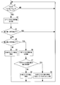
- FIG. 8 is a flowchart relating to frequency adjustment of the clock signal CLK in the configuration shown in FIG. 7 as described above.
- the rising / falling edge detection unit 302 detects the rising edge or the rising edge of the input clock signal CLKIN in step S1 of FIG. 8 (YES in step S1), the process proceeds to step S2.
- step S2 the controller 303 compares the counter value of the 8-bit counter 308 with the expected value.
- the process returns to the determination in step S1. If the difference between the counter value and the expected value is not equal to or less than the first predetermined value in step S3 (NO in step S3), the process proceeds to step S4.
- step S4 if the difference between the counter value and the expected value is not equal to or less than the second predetermined value (> first predetermined value) (NO in step S4), the controller 303 proceeds to step S5. In step S5, the controller 303 updates the value of the coarse adjustment command COARS. On the other hand, if the difference between the counter value and the expected value is equal to or less than the second predetermined value (YES in step S4), the process proceeds to step S6. In step S6, the controller 303 calculates the update value of the fine adjustment command FINE. Then, in step S7, it is determined whether the update value of the fine adjustment command FINE is the maximum value or the minimum value.
- step S7 If the update value is neither the maximum value nor the minimum value (NO in step S7), the process proceeds to step S8, and the controller 303 updates the value of the fine adjustment command FINE to the update value. On the other hand, if the update value is the maximum value or the minimum value (YES in step S7), the process proceeds to step S9, and the controller 303 centers the value of the fine adjustment command FINE while updating the value of the coarse adjustment command COARS. Let it be a value.
- LED drive device 30 semiconductor device
- a wafer test and a final test are performed as inspections before product shipment.
- the wafer test is a test performed before the circuit formed on the wafer is individualized into an IC chip.
- the frequency measurement of the clock signal CLK at the frequency center value setting, the frequency measurement of the clock signal CLK at the frequency maximum value setting, and the frequency minimum value setting are performed by the code setting by the coarse adjustment command COARS and the fine adjustment command FINE.
- the frequency of the clock signal CLK is measured in. The frequency measurement is performed, for example, by bringing the probe into contact with the electrode pad.
- a stack defect test of the mirror capacitance adjusting unit 241 is performed by the first self-diagnosis unit 311 described later. Since the stack defect test can be performed in a short time, it is preferable to include it in the wafer test.
- the final test is a test in the product state after packaging the IC chip, and like the wafer test, the frequency of the clock signal CLK is measured at each setting of the frequency center value, the maximum value, and the minimum value.
- a frequency linearity test between codes is performed by the second self-diagnosis unit 312 (FIG. 7) described later. It is also possible to include the linearity test by the second self-diagnosis unit 312 in the wafer test.
- the first self-diagnosis unit 311 and the second self-diagnosis unit 312 are circuits using BIST (Built-in Self Test).
- BIST is one of the design for testability (DFT) technologies.
- DFT design for testability
- the function of the IC tester is incorporated in the IC chip. Specifically, a "circuit that generates a test pattern" and a “circuit that collates the test result with the expected value" are integrated in the IC.
- FIG. 9 is a block diagram showing a configuration related to the test by the first self-diagnosis unit 311.
- FIG. 11 is a diagram showing an example of the internal configuration of the mirror capacitance adjusting unit 241.
- the mirror capacitance adjusting unit 241 has 16 capacitance units CU (1) to CU (16) and 15 capacitance units CU (17) to CU (31).
- the capacity units CU (1) to CU (16) are connected to the node Q1 (FIG. 7).
- the capacity units CU (17) to CU (31) are connected to the node Q2 (FIG. 7).
- FIG. 12 is a diagram showing an example of internal configuration of each capacity unit CU (*).
- the capacity unit CU (*) has a switch SW, a buffer BF, and a capacity C.
- the switch SW switches between conduction and interruption between node Q1 or node Q2 and one end of the capacitance C.
- the first self-diagnosis unit 311 converts the fine adjustment command FINE (5 bits) from the controller 303 into the setting signal DSET (31 bits).
- the on / off of the switch SW in each capacitance unit CU (*) is set according to the setting signal DSET. More specifically, for example, the capacitance units CU (1) to CU (16) in which the "1" and "0" of each bit from the least significant bit to the 16th bit of the setting signal DSET are connected to the node Q1, respectively.
- the setting signal DSET indicates that the switch SW of all the capacitance units CU (*) is off, and the fine adjustment command FINE is "1" (1) (.
- the setting signal DSET indicates that the switch SW of only the capacitance unit CU (1) is on, the switch SW of the remaining capacitance CU (*) is off, and the fine adjustment command FINE is "2" (.
- the setting signal DSET indicates that the switch SW of only the capacitance units CU (1) and CU (2) is on, and the switch SW of the remaining capacitance CU (*) is off. Every time the value (decimal number) of the fine adjustment command FINE is increased by 1, the capacity unit CU (*) in which the switch SW is turned on can be increased by one.
- the number of capacities C connected to the nodes Q1 and Q2 increases as the value of the fine adjustment command FINE increases. This makes it possible to adjust the mirror capacitance.
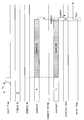
- FIG. 10 is a timing chart showing an example of a test operation by the first self-diagnosis unit 311.
- the fine adjustment command FINE is set to “0” at the start of the test, and the fixed command TCONT_IH output from the controller 303 is set to Low.
- the first self-diagnosis unit 311 converts the fixed command TCONT_IH into a fixed signal FIX, and instructs the selector 24F to select the fixed signal FIX from the output of the AND circuit 24E and the fixed signal FIX (FIG. FIG. 7).
- the fixed signal FIX is set to High, so the node Q1 is set to Low and the node Q2 is set to High.
- the fixed signal FIX is set to Low, so that the node Q1 is set to High and the node Q2 is set to Low.
- node Q1 is set to Low and node Q2 is set to High.
- the switches SW of all the capacitance units CU (*) are turned off.
- the output signal TIN formed based on the level of the signal output from the buffer BF in each capacitance unit CU (*) is output from the ring oscillator 24 (FIG. 9).
- the output signal TIN is 31-bit data corresponding to the number of capacitance units CU (*).
- the bit data of the output signal TIN is "1"
- the bit data of the output signal TIN is It is set to "0".
- the first self-diagnosis unit 311 compares the output signal TIN with the expected value after a predetermined time has elapsed from the start of the test in consideration of the time from the start of the test until the output signal TIN stabilizes.
- the first self-diagnosis unit 311 considers that there is no abnormality when the output signal TIN matches the expected value, outputs a judgment signal TOUT indicating normality to the controller 303, and when the output signal TIN does not match the expected value, there is an abnormality. Assuming that it has occurred, a determination signal TOUT indicating an abnormality is output to the controller 303.
- the determination signal TOUT is, for example, Low when it is normal, and High when it is abnormal. In addition, once the determination signal reaches a level indicating an abnormality, the level may be continued thereafter.
- the fine adjustment command FINE is maintained at "0"
- the fixed command TCONT_IH is switched to High
- node Q1 is set to High
- node Q2 is set to Low.
- the first self-diagnosis unit 311 compares the output signal TIN with the expected value and outputs the determination signal TOUT.
- the fine adjustment command FINE is switched to "1"
- the fixed command TCONT_IH is switched to Low
- node Q1 is set to Low
- node Q2 is set to High.
- the switch SW of only the capacitance unit CU (1) is turned on.
- the first self-diagnosis unit 311 compares the output signal TIN with the expected value and outputs the determination signal TOUT.
- the fine adjustment command FINE is maintained at "1"
- the fixed command TCONT_IH is switched to High
- node Q1 is set to High
- node Q2 is set to Low.
- the first self-diagnosis unit 311 compares the output signal TIN with the expected value and outputs the determination signal TOUT.
- the level of the nodes Q1 and Q2 is switched while the fine adjustment command FINE is switched, and the output signal TIN is determined.
- FIG. 13 is a diagram showing a configuration example of the second self-diagnosis unit 312.
- the second self-diagnosis unit 312 has an 11-bit counter 312A, a 13-bit counter 312B, a selector 312C, a previous data storage unit 312D, and a comparison unit 312E.
- the value of the coarse adjustment command COARS is changed by keeping the value of the fine adjustment command FINE output from the controller 303 constant, or the value of the coarse adjustment command COARS is changed.
- the frequency of the clock signal CLK is measured by changing the value of the fine adjustment command FINE as a constant, and the frequency linearity between the codes is confirmed.
- the ring oscillator 24 is in the same state as in normal operation, and the selector 24F selects the output of the AND circuit 24E (FIG. 7).
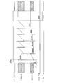
- FIG. 14 is a timing chart showing an example of a test operation when the fine adjustment command FINE is changed while the coarse adjustment command COARS is constant. As shown in FIG. 14, the value of the fine adjustment command FINE is switched at the timing t10. When the stabilization time Ts required for stabilizing the frequency of the clock signal CLK elapses from the timing t10, the start flag is raised. After that, when the start flag goes down (timing t11), the controller 303 causes the 11-bit counter 312A and the 13-bit counter 312B to start counting.
- the 11-bit counter 312A counts 5 MHz signals.
- the 13-bit counter 312B counts the clock signal CLK.
- the comparison timing signal output from the 11-bit counter 312A rises to High.
- the comparison unit 312E compares the counter value by the 13-bit counter 312B at that time with the counter value stored in the previous data storage unit 312D.
- the time required to count the 5 MHz signal for 11 bits is 409.6 ⁇ s, and the frequency of the clock signal CLK is specified by the counter value counted by the 13-bit counter 312B during the time. That is, the 13-bit counter 312B corresponds to a measuring unit that measures the frequency of the clock signal CLK.
- the counter value in the fine adjustment command FINE before the value of the fine adjustment command FINE is switched at the timing t10 is saved in the previous data storage unit 312D, and the counter value is compared by the comparison unit to clock the clocks between the codes. The change in the frequency of the signal CLK can be determined.
- the comparison unit 312E since there is no abnormality in the change in the frequency of the clock signal CLK by the comparison by the comparison unit 312E, the comparison unit 312E notifies the controller 303 that it is normal, and the controller 303 indicates Low. Error flag is output.
- the selector 312C selects the counter value of the 13-bit counter 312B and overwrites the previous data storage unit 312D (previous data update). After that, since the selector 312C selects the output of the previous data storage unit 312D, the data of the previous data storage unit 312D does not change.
- FIG. 16 is a timing chart showing an example of the change pattern of the code (fine adjustment command FINE, coarse adjustment command COARS) in the test using the second self-diagnosis unit 312.
- the normal operation is switched to the test operation, the value of the fine adjustment command FINE is set to "10000", and the coarse adjustment command COARS is set to "0000".
- the stabilization time Ts elapses from the timing t20, counting by the 11-bit counter 312A and the 13-bit counter 312B is started, and the counter value is stored in the previous data storage unit 312D.
- the comparison by the comparison unit 312E is not performed.
- the coarse adjustment command COARS is switched to "00001" while maintaining the value of the fine adjustment command FINE.
- counting by the 11-bit counter 312A and the 13-bit counter 312B is started at the timing when the stabilization time Ts has elapsed from the timing when the coarse adjustment command COARS is switched.
- the new counter value by the 13-bit counter 312B is compared with the counter value of the previous data storage unit 312D. At this time, the new counter value is overwritten and saved in the previous data storage unit 312D.
- the value of the coarse adjustment command COARS is sequentially switched to "11111" to compare the counter values.
- the value of the fine adjustment command FINE is switched to "00001" while maintaining the value of the coarse adjustment command COARS.
- counting by the 11-bit counter 312A and the 13-bit counter 312B is started at the timing when the stabilization time Ts elapses from the timing when the value of the fine adjustment command FINE is switched.
- the new counter value by the 13-bit counter 312B is compared with the counter value of the previous data storage unit 312D. At this time, the new counter value is overwritten and saved in the previous data storage unit 312D.
- the value of the fine adjustment command FINE is sequentially switched to "11111" to compare the counter values.
- the value of the fine adjustment command FINE is switched to "11111"
- the value of the fine adjustment command FINE is switched to "00000”
- the value of the coarse adjustment command COARS is switched to "00110".
- the comparison is not performed by the comparison unit 312E, and the counter value is stored in the previous data storage unit 312D.
- the value of the fine adjustment command FINE is sequentially switched to "11111" to compare the counter values.
- the value of the coarse adjustment command COARS is switched in the order of "01100”, “10000”, “10110”, “11100”, “11111”, and the fine adjustment command FINE is performed while the value of the coarse adjustment command COARS is constant.
- the counter values are compared while switching the value of.
- the LED drive device 30 shown in FIG. 1 is a packaged product having a rectangular shape when viewed from above. Of the two opposite sides of the rectangular shape, the PWMIN terminal is arranged on one side, and the PWMOUT terminal is arranged on the other side.
- the PWM OUT terminal is arranged on the same side as the side on which the FBV terminal is arranged, it is desirable that at least one terminal is arranged between the PWM OUT terminal and the FBV terminal.
- the PWMOUT terminal is arranged on the same side as the side on which the MINSELV terminal is arranged, it is desirable that at least one terminal is arranged between the PWMOUT terminal and the MINSELV terminal. That is, it is desirable that the PWMOUT terminal is not adjacent to the FBV terminal and the MINSELV terminal. This is because the signal generated at the PWM OUT terminal is a rectangular wave, whereas the signal generated at the FBV terminal and the MINSELV terminal is an analog signal.
- the PWM OUT terminal is a low withstand voltage terminal
- the PGND terminal, SW terminal, GH terminal, BOOT terminal, VIN terminal, SNSP terminal, SNSN terminal, and COMP terminal are high withstand voltage terminals, which may cause a short circuit between the terminals.
- the PWMOUT terminal is arranged on the same side as the side on which any of the LED terminals 1 to LED24 (for example, LED13 to LED24 terminals) is arranged, at least one terminal is connected to the LED terminal. Is desirable to be placed. That is, it is desirable that the PWM OUT terminal is not adjacent to the LED terminal. This is because a high voltage is applied to the LED terminal.
- the present invention can be used as an example for driving a vehicle-mounted LED.
Landscapes
- Engineering & Computer Science (AREA)
- Theoretical Computer Science (AREA)
- Physics & Mathematics (AREA)
- General Engineering & Computer Science (AREA)
- General Physics & Mathematics (AREA)
- Mathematical Physics (AREA)
- Computer Hardware Design (AREA)
- Led Devices (AREA)
Priority Applications (4)
| Application Number | Priority Date | Filing Date | Title |
|---|---|---|---|
| DE112020006500.6T DE112020006500T9 (de) | 2020-01-10 | 2020-12-29 | Halbleiterelement und einrichtung für halbleiterelement |
| US17/791,634 US11874694B2 (en) | 2020-01-10 | 2020-12-29 | Semiconductor device and semiconductor device system |
| JP2021570039A JPWO2021140998A1 (https=) | 2020-01-10 | 2020-12-29 | |
| CN202080092477.0A CN114930268B (zh) | 2020-01-10 | 2020-12-29 | 半导体器件和半导体器件系统 |
Applications Claiming Priority (2)
| Application Number | Priority Date | Filing Date | Title |
|---|---|---|---|
| JP2020003169 | 2020-01-10 | ||
| JP2020-003169 | 2020-01-10 |
Publications (1)
| Publication Number | Publication Date |
|---|---|
| WO2021140998A1 true WO2021140998A1 (ja) | 2021-07-15 |
Family
ID=76787961
Family Applications (1)
| Application Number | Title | Priority Date | Filing Date |
|---|---|---|---|
| PCT/JP2020/049287 Ceased WO2021140998A1 (ja) | 2020-01-10 | 2020-12-29 | 半導体装置、および半導体装置システム |
Country Status (5)
| Country | Link |
|---|---|
| US (1) | US11874694B2 (https=) |
| JP (1) | JPWO2021140998A1 (https=) |
| CN (1) | CN114930268B (https=) |
| DE (1) | DE112020006500T9 (https=) |
| WO (1) | WO2021140998A1 (https=) |
Families Citing this family (3)
| Publication number | Priority date | Publication date | Assignee | Title |
|---|---|---|---|---|
| CN117093264A (zh) * | 2022-05-13 | 2023-11-21 | 长鑫存储技术有限公司 | 片选信号的生成方法及设备 |
| US12406120B2 (en) * | 2022-09-27 | 2025-09-02 | Synopsys, Inc. | Multicycle path prediction of reset signals |
| KR20250129006A (ko) * | 2022-12-23 | 2025-08-28 | 뷰리얼 인크. | 운송 차량에서 can 버스 및 액추에이터와 통합된 마이크로-led |
Citations (5)
| Publication number | Priority date | Publication date | Assignee | Title |
|---|---|---|---|---|
| JP2009200661A (ja) * | 2008-02-20 | 2009-09-03 | Hitachi Ltd | 半導体集積回路装置および逓倍クロック生成方法 |
| JP2012203866A (ja) * | 2011-03-28 | 2012-10-22 | Renesas Electronics Corp | クロック生成回路、それを用いたプロセッサシステム、及びクロック周波数制御方法 |
| US20160135264A1 (en) * | 2014-11-07 | 2016-05-12 | Power Integrations, Inc. | Enable circuit for lighting drivers |
| JP2016154399A (ja) * | 2015-02-20 | 2016-08-25 | オムロンオートモーティブエレクトロニクス株式会社 | 電圧変換装置 |
| JP2019192498A (ja) * | 2018-04-25 | 2019-10-31 | シャープ株式会社 | Ledモジュールおよびバックライト装置 |
Family Cites Families (17)
| Publication number | Priority date | Publication date | Assignee | Title |
|---|---|---|---|---|
| US20020102957A1 (en) * | 2001-01-29 | 2002-08-01 | Han-Yang Tseng | Radio signal receiving control device and the control method for the same |
| US7336752B2 (en) * | 2002-12-31 | 2008-02-26 | Mosaid Technologies Inc. | Wide frequency range delay locked loop |
| US7177611B2 (en) * | 2004-07-07 | 2007-02-13 | Texas Instruments Incorporated | Hybrid control of phase locked loops |
| JP2006039830A (ja) * | 2004-07-26 | 2006-02-09 | Renesas Technology Corp | 半導体集積回路 |
| JP2006191372A (ja) * | 2005-01-06 | 2006-07-20 | Matsushita Electric Ind Co Ltd | デュアルループpllおよび逓倍クロック発生装置 |
| JP4751178B2 (ja) * | 2005-10-27 | 2011-08-17 | エルピーダメモリ株式会社 | 同期型半導体装置 |
| KR100843197B1 (ko) * | 2006-02-28 | 2008-07-02 | 삼성전자주식회사 | 위상이 다른 다수개의 드라우지 클럭 신호들을 내부적으로발생하는 집적회로 장치 |
| JP2008099002A (ja) * | 2006-10-12 | 2008-04-24 | Elpida Memory Inc | Dll回路 |
| JP4569656B2 (ja) * | 2008-03-28 | 2010-10-27 | ソニー株式会社 | 遅延同期ループ回路および表示装置 |
| US8073092B2 (en) * | 2008-06-19 | 2011-12-06 | Microchip Technology Incorporated | Automatic synchronization of an internal oscillator to an external frequency reference |
| KR101035856B1 (ko) * | 2010-05-31 | 2011-05-19 | 주식회사 아나패스 | 타이밍 컨트롤러와 데이터 구동ic들 사이의 인터페이스 시스템 및 디스플레이 장치 |
| KR101193305B1 (ko) * | 2011-08-02 | 2012-10-19 | 삼성전기주식회사 | 디밍제어장치, 엘이디 구동장치 및 디밍제어방법 |
| US8315128B1 (en) * | 2012-01-09 | 2012-11-20 | Lsi Corporation | Heat assisted magnetic recording system |
| US9013113B2 (en) * | 2012-04-20 | 2015-04-21 | Apple Inc. | Keyboard backlight driver IC |
| US11150236B2 (en) * | 2016-02-19 | 2021-10-19 | University Of Massachusetts | Multi-well quartz crystal microbalance mass and viscoelastic sensor |
| JP2019179662A (ja) | 2018-03-30 | 2019-10-17 | 株式会社デンソーテン | 光源駆動装置および光源駆動方法 |
| US11271572B2 (en) * | 2020-04-29 | 2022-03-08 | Analog Devices International Unlimited Company | Self-tuning phase-locked loop (PLL) circuit |
-
2020
- 2020-12-29 JP JP2021570039A patent/JPWO2021140998A1/ja active Pending
- 2020-12-29 WO PCT/JP2020/049287 patent/WO2021140998A1/ja not_active Ceased
- 2020-12-29 US US17/791,634 patent/US11874694B2/en active Active
- 2020-12-29 CN CN202080092477.0A patent/CN114930268B/zh active Active
- 2020-12-29 DE DE112020006500.6T patent/DE112020006500T9/de active Active
Patent Citations (5)
| Publication number | Priority date | Publication date | Assignee | Title |
|---|---|---|---|---|
| JP2009200661A (ja) * | 2008-02-20 | 2009-09-03 | Hitachi Ltd | 半導体集積回路装置および逓倍クロック生成方法 |
| JP2012203866A (ja) * | 2011-03-28 | 2012-10-22 | Renesas Electronics Corp | クロック生成回路、それを用いたプロセッサシステム、及びクロック周波数制御方法 |
| US20160135264A1 (en) * | 2014-11-07 | 2016-05-12 | Power Integrations, Inc. | Enable circuit for lighting drivers |
| JP2016154399A (ja) * | 2015-02-20 | 2016-08-25 | オムロンオートモーティブエレクトロニクス株式会社 | 電圧変換装置 |
| JP2019192498A (ja) * | 2018-04-25 | 2019-10-31 | シャープ株式会社 | Ledモジュールおよびバックライト装置 |
Also Published As
| Publication number | Publication date |
|---|---|
| DE112020006500T9 (de) | 2023-01-19 |
| US20230066399A1 (en) | 2023-03-02 |
| JPWO2021140998A1 (https=) | 2021-07-15 |
| DE112020006500T5 (de) | 2022-12-01 |
| CN114930268A (zh) | 2022-08-19 |
| CN114930268B (zh) | 2024-05-17 |
| US11874694B2 (en) | 2024-01-16 |
Similar Documents
| Publication | Publication Date | Title |
|---|---|---|
| US8493050B2 (en) | Control circuit for switching power supply unit, electronic device and method for controlling switching power supply unit | |
| US20210028686A1 (en) | Fault protection method used in multiphase switching converters with daisy chain configuration | |
| US9520765B2 (en) | DC/DC converter, switching power supply device, and electronic apparatus,configured to include a phase detector and a phase holder | |
| US6982886B2 (en) | Dc-ac converter parallel operation system and controller ic therefor | |
| WO2021140998A1 (ja) | 半導体装置、および半導体装置システム | |
| US9837897B2 (en) | Buck converter | |
| US8233297B2 (en) | Multi-stage power supply | |
| US8760137B2 (en) | DC-DC converter control circuit and DC-DC converter including same | |
| US10122254B2 (en) | Devices, systems and processes for average current control | |
| JP2019017241A (ja) | スイッチング信号の同期システムおよび同期方法 | |
| JP2015525059A (ja) | 電力供給システムおよび方法 | |
| US8248139B2 (en) | Simple interleaved phase shift clock synchronization for master/slave scheme | |
| EP2973971A2 (en) | Systems and methods for 100 percent duty cycle in switching regulators | |
| US12407260B2 (en) | Power supply system apparatus | |
| US20190159308A1 (en) | Line ripple reducer | |
| EP3206301B1 (en) | Oscillation circuit | |
| CN103023311B (zh) | 电源装置和发光元件驱动装置 | |
| WO2020236712A1 (en) | Multiple dithering profile signal generation | |
| US20070090774A1 (en) | Discharge lamp driving device and driving method | |
| US11394428B2 (en) | Power regulation for lighting using NFC | |
| KR20010050573A (ko) | 히스테리 스위치-모드 전원의 주파수 제어 | |
| JP2021010294A (ja) | 補償電流校正裝置 | |
| US8421511B2 (en) | Power converter and pulse width modulation signal controlling apparatus thereof | |
| JP2025097880A (ja) | パワーアンプの保護回路、供給電圧調整方法及び電子装置 | |
| JP2000175447A (ja) | 半導体集積回路装置 |
Legal Events
| Date | Code | Title | Description |
|---|---|---|---|
| 121 | Ep: the epo has been informed by wipo that ep was designated in this application |
Ref document number: 20911740 Country of ref document: EP Kind code of ref document: A1 |
|
| ENP | Entry into the national phase |
Ref document number: 2021570039 Country of ref document: JP Kind code of ref document: A |
|
| 122 | Ep: pct application non-entry in european phase |
Ref document number: 20911740 Country of ref document: EP Kind code of ref document: A1 |