WO2021140998A1 - 半導体装置、および半導体装置システム - Google Patents
半導体装置、および半導体装置システム Download PDFInfo
- Publication number
- WO2021140998A1 WO2021140998A1 PCT/JP2020/049287 JP2020049287W WO2021140998A1 WO 2021140998 A1 WO2021140998 A1 WO 2021140998A1 JP 2020049287 W JP2020049287 W JP 2020049287W WO 2021140998 A1 WO2021140998 A1 WO 2021140998A1
- Authority
- WO
- WIPO (PCT)
- Prior art keywords
- clock signal
- terminal
- semiconductor device
- unit
- frequency
- Prior art date
Links
Images


Classifications
-
- H—ELECTRICITY
- H05—ELECTRIC TECHNIQUES NOT OTHERWISE PROVIDED FOR
- H05B—ELECTRIC HEATING; ELECTRIC LIGHT SOURCES NOT OTHERWISE PROVIDED FOR; CIRCUIT ARRANGEMENTS FOR ELECTRIC LIGHT SOURCES, IN GENERAL
- H05B45/00—Circuit arrangements for operating light-emitting diodes [LED]
- H05B45/30—Driver circuits
- H05B45/37—Converter circuits
- H05B45/3725—Switched mode power supply [SMPS]
- H05B45/375—Switched mode power supply [SMPS] using buck topology
-
- G—PHYSICS
- G06—COMPUTING; CALCULATING OR COUNTING
- G06F—ELECTRIC DIGITAL DATA PROCESSING
- G06F1/00—Details not covered by groups G06F3/00 - G06F13/00 and G06F21/00
- G06F1/04—Generating or distributing clock signals or signals derived directly therefrom
- G06F1/08—Clock generators with changeable or programmable clock frequency
-
- G—PHYSICS
- G06—COMPUTING; CALCULATING OR COUNTING
- G06F—ELECTRIC DIGITAL DATA PROCESSING
- G06F1/00—Details not covered by groups G06F3/00 - G06F13/00 and G06F21/00
- G06F1/04—Generating or distributing clock signals or signals derived directly therefrom
- G06F1/12—Synchronisation of different clock signals provided by a plurality of clock generators
-
- G—PHYSICS
- G06—COMPUTING; CALCULATING OR COUNTING
- G06F—ELECTRIC DIGITAL DATA PROCESSING
- G06F1/00—Details not covered by groups G06F3/00 - G06F13/00 and G06F21/00
- G06F1/26—Power supply means, e.g. regulation thereof
- G06F1/28—Supervision thereof, e.g. detecting power-supply failure by out of limits supervision
-
- G—PHYSICS
- G06—COMPUTING; CALCULATING OR COUNTING
- G06F—ELECTRIC DIGITAL DATA PROCESSING
- G06F13/00—Interconnection of, or transfer of information or other signals between, memories, input/output devices or central processing units
- G06F13/38—Information transfer, e.g. on bus
- G06F13/40—Bus structure
- G06F13/4004—Coupling between buses
- G06F13/4022—Coupling between buses using switching circuits, e.g. switching matrix, connection or expansion network
-
- H—ELECTRICITY
- H05—ELECTRIC TECHNIQUES NOT OTHERWISE PROVIDED FOR
- H05B—ELECTRIC HEATING; ELECTRIC LIGHT SOURCES NOT OTHERWISE PROVIDED FOR; CIRCUIT ARRANGEMENTS FOR ELECTRIC LIGHT SOURCES, IN GENERAL
- H05B45/00—Circuit arrangements for operating light-emitting diodes [LED]
- H05B45/30—Driver circuits
- H05B45/32—Pulse-control circuits
- H05B45/325—Pulse-width modulation [PWM]
-
- H—ELECTRICITY
- H05—ELECTRIC TECHNIQUES NOT OTHERWISE PROVIDED FOR
- H05B—ELECTRIC HEATING; ELECTRIC LIGHT SOURCES NOT OTHERWISE PROVIDED FOR; CIRCUIT ARRANGEMENTS FOR ELECTRIC LIGHT SOURCES, IN GENERAL
- H05B45/00—Circuit arrangements for operating light-emitting diodes [LED]
- H05B45/50—Circuit arrangements for operating light-emitting diodes [LED] responsive to malfunctions or undesirable behaviour of LEDs; responsive to LED life; Protective circuits
Definitions
- the present invention relates to a semiconductor device having an oscillator.
- a semiconductor device formed including a semiconductor integrated circuit is often provided with an oscillator that generates a clock signal.
- a PWM (Pulse Width Modulation) signal can be generated based on a clock signal.
- the semiconductor device is, for example, an LED (Light Emitting Diode) drive device (LED driver)
- LED driver Light Emitting Diode
- An example of an LED drive device having a PWM dimming function is disclosed in Patent Document 1.
- a system may be configured by using a plurality of the above semiconductor devices.
- the frequency of the clock signal generated by the oscillator included in each semiconductor device varies. If the frequency of the clock signal varies, for example, the PWM signal may not be synchronized. In this case, for example, there is a possibility that a defect may occur in the image formed by the PWM dimming of the LED.
- each semiconductor device is a crystal oscillator, it is possible to suppress the variation in the frequency of the clock signal, but it is disadvantageous in terms of cost.
- an object of the present invention is to provide a semiconductor device capable of synchronizing the frequencies of clock signals generated in each semiconductor device even when a plurality of semiconductor devices are used.
- the semiconductor device is The oscillator that generates the first clock signal and The first terminal to which the input clock signal is input from the outside and A first counter that counts a clock signal based on the first clock signal between the edges of the input clock signal, and A controller that sends a command for adjusting the frequency of the first clock signal to the oscillator based on the result of comparison between the counter value and the expected value by the first counter. (First configuration).
- the configuration may include a selector that selects and outputs as an output clock signal, and a second terminal that outputs the output clock signal to the outside (second configuration).
- the frequency dividing unit divides the output of the first frequency divider and the output of the first frequency divider by the first frequency dividing device.
- a second frequency divider that divides by ratio, The first counter may be configured to count the output of the first frequency divider (third configuration).
- the frequency dividing portion may be configured to generate the second clock signal whose duty is restricted to a predetermined value (fourth configuration).
- one of the selection of the input clock signal by the selector, the selection of the second clock signal, and the selection of not outputting the output clock signal can be set. (Fifth configuration).
- the oscillator may be a ring oscillator (sixth configuration).
- the ring oscillator has an odd number of inverters, a DAC (DA converter) that DA-converts a rough adjustment command from the controller, and a current corresponding to the output of the DAC to the inverter.
- the configuration may include a current supply unit for flowing current and a mirror capacity adjustment unit for changing the capacity value connected to the node between the inverters based on the fine adjustment command from the controller (seventh configuration).
- the mirror capacity adjusting unit has a plurality of capacity units including a capacity and a switch arranged between the capacity and the node, and the semiconductor device includes a plurality of capacity units.
- a configuration further including a first self-diagnosis unit that applies Low and High voltages to the node while changing the pattern of the capacitance unit that turns on the switch, and compares the output from the capacitance unit with the expected value.
- a measuring unit that measures the frequency of the first clock signal in a test operation in which the controller keeps one of the coarse adjustment command and the fine adjustment command constant and changes the other.
- a second self-diagnosis unit including a comparison unit for comparing the measurement results of the measurement unit before and after the change of the command may be provided (nineth configuration).
- the second self-diagnosis unit includes a second counter of a predetermined bit for counting a signal having a predetermined frequency, and the measuring unit includes a period during which the second counter counts the predetermined bit.
- the third counter that counts the first clock signal may be configured (10th configuration).
- a configuration may include a PWM signal generation unit that generates a PWM signal based on the first clock signal (11th configuration).
- the PWM signal generation unit may be configured to form the edge of the PWM signal when the edge of the input clock signal is detected (12th configuration).
- the LED terminal to which the cathode of the LED can be connected and the current driver for controlling the current flowing through the LED terminal are provided, and the current driver responds to the PWM signal. It may be configured to be turned on and off (13th configuration).
- the semiconductor device system includes a plurality of semiconductor devices having the thirteenth configuration, and each of the plurality of semiconductor devices is externally connected to the semiconductor device via a CAN (Controller Area Network) transceiver.
- the on-duty of the PWM signal is commanded (14th configuration).
- the semiconductor device system includes a plurality of semiconductor devices having any of the second to fifth configurations, the second terminal of the semiconductor device on the front stage side and the second terminal on the rear stage side.
- the configuration is such that the first terminal of the semiconductor device is connected (15th configuration).
- the semiconductor device system having the fifteenth configuration may be for in-vehicle use.
- the semiconductor device of the present invention even when a plurality of semiconductor devices are used, it is possible to synchronize the frequencies of clock signals generated in the individual semiconductor devices.
- FIG. 1 It is a figure which shows the structure of the LED drive device which concerns on an exemplary embodiment of this invention. It is a figure which shows an example of the case where a plurality of LED drive devices are connected and used. It is a figure which shows the system configuration example when the LED drive device is applied to the rear lamp of a vehicle. It is a block diagram which shows the structure about the frequency synchronization of the clock signal in the LED drive device. It is a table which shows the correspondence relationship between the setting data SYNCSET set in the register, the valid / invalid of the PWMIN terminal, and the valid / invalid of the PWMOUT terminal. It is a figure which shows an example of the structure which connected a plurality of LED drive devices.
- the coarse adjustment command COARS is a timing chart showing an example of a test operation when the fine adjustment command FINE is changed while being constant (when normal).
- the coarse adjustment command COARS is a timing chart showing an example of a test operation when the fine adjustment command FINE is changed while being constant (in the case of an abnormality). It is a timing chart which shows an example of the code change pattern in the test using the 2nd self-diagnosis part (when it is normal). It is a timing chart which shows an example of the code change pattern in the test using the 2nd self-diagnosis part (in the case of abnormality occurrence).
- the fine adjustment command FINE is a diagram showing a count start timing when the coarse adjustment command COARS is constantly changed.
- the coarse adjustment command COARS is a diagram showing a count start timing when the fine adjustment command FINE is changed constantly.
- FIG. 1 is a diagram showing a configuration of an LED drive device 30 according to an exemplary embodiment of the present invention.
- the LED driving device 30 shown in FIG. 1 drives LED arrays A1 to A24 having a plurality of channels (24 channels as an example in this embodiment).
- the LED drive device 30 is for in-vehicle use as an example.
- the LED drive device 30 includes a minimum voltage selection unit 1, a reference voltage generation unit 2, a spectrum diffusion reference voltage generation unit 3, a frequency / voltage conversion unit 4, an error amplifier 5, a ripple injection unit 6, and an amplifier. 7, Low side comparator 8, High side comparator 9, RS flip flop 10, OCP (overcurrent protection) unit 11, driver logic unit 12, diode 13, driver 14, SWOCP unit 15, NMOS transistor 16, UVLO (Under Voltage Lock Out) / TSD (Thermal Shut Down) section 17, band gap reference 18, internal voltage generator 19, internal voltage generator 20, anomaly notification section 21, and NMOS.
- a semiconductor integrated circuit that integrates a transistor 22, an I / O (input / output) port 23, a ring oscillator 24, a control logic unit 25, a current driver 26, a short detection unit 27, and an open detection unit 28. It is a semiconductor device having (IC chip).
- the LED drive device 30 has, as external terminals for establishing an electrical connection with the outside, a COMP terminal, an SNSN terminal, an SNSP terminal, a BOOT terminal, a GH terminal, a SW terminal, a PGND terminal, a VIN terminal, a VREG5 terminal, and the like. It has VREG3 terminal, FAILB terminal, EN terminal, RX terminal, TX terminal, CS0 to CS3 terminal, PWMIN terminal, FBV terminal, MINSELV terminal, LED1 to LED24 terminal, LGND1 to LGND4 terminal, PWMOUT terminal, and GND terminal. There is.
- an output stage 35 for generating an output voltage Vout from the input voltage Vin by DC / DC conversion and supplying it to the anodes of the LED arrays A1 to A24 is arranged.
- Each of the output stages 35 is a discrete component and includes a switching element N1, a diode D1, an inductor L1, a resistor R1, and an output capacitor Co. Since the switching element N1 is driven and controlled by the LED driving device 30, the output stage 35 is controlled by the LED driving device 30.
- a DC / DC converter is formed by the output stage 35 and the LED drive device 30.
- an asynchronous rectifying type step-down DC / DC converter is particularly configured as the DC / DC converter.
- the drain of the switching element N1 composed of the NMOS transistor is connected to the application end of the input voltage Vin.
- the node Nd1 to which the source of the switching element N1 and the cathode of the diode D1 are connected is connected to the SW terminal.
- the anode of the diode D1 is connected to the application end of the ground potential.
- the node Nd1 is connected to one end of the inductor L1.
- the other end of the inductor L1 is connected to one end of the resistor R1 by a node Nd2.
- the other end of the resistor R1 is connected to one end of the output capacitor Co by the node Nd3.
- the other end of the output capacitor Co is connected to the end where the ground potential is applied.
- the gate of the switching element N1 is connected to the output end of the driver 14 via the GH terminal.
- the low potential side of the driver 14 is connected to the SW terminal.
- the high potential side of the driver 14 is connected to the cathode of the diode 13.
- the anode of the diode 13 is connected to the application end of the reference voltage Vdrv5.
- One end of the boot capacitor Cb is connected between the inductor L1 and the node Nd1.
- the other end of the boot capacitor Cb is connected to the cathode of the diode 13 via the BOOT terminal.
- the switching element N1 is turned on. At this time, a voltage higher than the voltage generated in the boot capacitor Cb by charging from the input voltage Vin is generated in the BOOT terminal. This makes it possible to turn on the switching element N1 which is an NMOS transistor.
- the output voltage Vout is generated at the node Nd3 by such on / off control of the switching element N1.
- each cathode of the LED arrays A1 to A24 is connected to the LED1 to LED24 terminals, respectively.
- the minimum voltage selection unit 1 selects the minimum voltage among the terminal voltages (cathode voltage) of the LEDs 1 to 24.
- the node Nd2 to which one end of the resistor R1 is connected is connected to the SNSP terminal.
- the node Nd3 to which the other end of the resistor R1 is connected is connected to the SNSN terminal.
- the SNSP terminal voltage and the SNSN terminal voltage are input to the amplifier 7.
- the amplifier 7 amplifies and outputs the voltage difference between the SNSP terminal voltage and the SNSN terminal voltage. As a result, the amplifier 7 detects the inductor current flowing through the inductor L1 (resistor R1).
- the ripple injection unit 6 injects ripple into the minimum voltage selected by the minimum voltage selection unit 1 based on the output of the amplifier 7.
- the minimum voltage after injecting the ripple is input to the inverting input end ( ⁇ ) of the Low side comparator 8 and input to the non-inverting input end (+) of the High side comparator 9.
- the output of the Low side comparator 8 is input to the reset terminal of the RS flip-flop 10.
- the output of the High side comparator 9 is input to the set terminal of the RS flip-flop 10.
- the flip-flop output signal FFOUT is output from the Q output terminal of the RS flip-flop 10.
- the driver logic unit 12 controls the switching element N1 via the driver 14 based on the flip-flop output signal FFOUT.
- the frequency / voltage conversion unit 4 converts the frequency of the flip-flop output signal FFOUT into a voltage signal and outputs it to the non-inverting input terminal (+) of the error amplifier 5.
- the output of the spread spectrum reference voltage generation unit 3 is input to the inverting input terminal (-) of the error amplifier 5.
- the reference voltage generation unit 2 variably generates the Low side reference voltage VrefL and the High side reference voltage VrefH based on the output of the error amplifier 5.
- the Low side reference voltage VrefL is input to the non-inverting input end (+) of the Low side comparator 8.
- the high-side reference voltage VrefH is input to the inverting input end ( ⁇ ) of the high-side comparator 9.
- hysteresis control (Bang-Bang control) is performed, and the minimum voltage among the cathode voltages of the LED arrays A1 to A24 is controlled to a desired voltage. Further, by changing the switching frequency with time by the spread spectrum reference voltage generation unit 3, it is possible to disperse the spectrum frequency, suppress the peak of the spectrum power, and take EMI (Electro Magnetic Interference) measures. ..
- FIG. 2A shows, as an example, a configuration in which three LED drive devices 30 (30 m, 30s1, 30s2) are connected and used.
- the LED drive device 30m corresponds to the master described later
- the LED drive devices 30s1 and 30s2 correspond to the slave described later.
- Each cathode of the LED arrays A1 to A24 is connected to each of the LED drive devices 30m, 30s1 and 30s2.
- An output voltage Vout generated by the DC / DC function in the LED drive device 30 m is applied to each anode of the LED arrays A1 to A24.
- the DC / DC function is not used in the LED drive devices 30s1 and 30s2.
- FIG. 2A the configuration relating to the output of the output voltage Vout is shown in a simplified manner for convenience.
- the FBV terminal outputs the respective cathode voltages of the LED arrays A1 to A24 and the minimum voltage selected by the minimum selection unit 1 among the voltages of the MINSELV terminals.
- the FBV terminal of the external LED drive device 30 is connected to the MINSELV terminal.
- the MINSELV terminal of the LED drive device 30 m is connected to the FBV terminal of the LED drive device 30s1, and the MINSELV terminal of the LED drive device 30s1 is connected to the FBV terminal of the LED drive device 30s2.
- the FBV terminal of the LED drive device 30 m and the MINSELV terminal of the LED drive device 30s2 are not connected.
- the MINSELV terminal of the LED drive device 30s2 should be connected to an application end of a high gain voltage such as the reference voltage Vdrv5 generated at the VREG5 terminal of the LED drive device 30s2 so as not to affect the selection of the minimum voltage. Is desirable.
- the minimum voltage among the cathode voltages of the LED arrays A1 to A24 is selected, and the selected minimum voltage is output from its own FBV terminal.
- the voltage input from the FBV terminal of the LED drive device 30s2 to its own MINSELV terminal and the minimum voltage among the cathode voltages of the LED arrays A1 to A24 are selected, and the selected minimum voltage is itself. It is output from the FBV terminal of.
- the voltage input from the FBV terminal of the LED drive device 30s1 to its own MINSELV terminal and the minimum voltage among the cathode voltages of the LED arrays A1 to A24 are selected, and the selected minimum voltage is DC. / Used for DC function.
- the OCP unit 11 detects the overcurrent based on the detection result of the inductor current by the amplifier 7 and protects it.
- the SWOCP unit 15 is a circuit that detects an overcurrent flowing through the switching element N1.
- the NMOS transistor 16 is connected between the SW terminal and the PGND terminal.
- the PGND terminal is connected to the ground potential.
- the UVLO / TSD unit 17 monitors the input voltage Vin to perform low voltage protection, and monitors the junction temperature of the LED drive device 30 to perform overheat protection.
- the input voltage Vin is generated based on the battery power supply B and applied to the VIN terminal.
- the bandgap reference 18 is a reference voltage source that generates a stable reference voltage Vbg based on the input voltage Vin applied to the VIN terminal.
- the internal voltage generation unit 19 generates a reference voltage Vdrv5 of 5V based on the input voltage Vin.
- the output end of the internal voltage generator 19 is connected to the capacitor via the VREG5 terminal.
- the internal voltage generation unit 20 generates a reference voltage Vref 33 of 3.3 V based on the reference voltage Vdrv5.
- the output end of the internal voltage generator 20 is connected to a capacitor via the VREG3 terminal.
- the MCU (Micro Controller Unit) 45 and the CAN (Controller Area Network) transceiver 40 are arranged outside the LED drive device 30.
- the NMOS transistor 22 is pulled up by a resistor to the reference voltage Vref 33 generated at the VREG3 terminal.
- the abnormality notification unit 21 notifies the MCU 45 of a Low abnormality signal fat indicating an abnormality by turning on the NMOS transistor 22 based on a command from the control logic unit 25.
- the MCU 45 transmits an enable signal enable to the control logic unit 25 via the EN terminal and the I / O port 23.
- the CAN transceiver 40 transmits data received from the MCU 45 via the CAN bus CB to the RX terminal as received data Rxd.
- the control logic unit 25 receives the received data Rxd via the I / O port 23.
- the control logic unit 25 transmits the transmission data Txd to the TX terminal via the I / O port 23.
- the CAN transceiver 40 transmits the transmission data Txd received from the TX terminal to the MCU 45 via the CAN bus CB.
- the I / O port 23 is configured as a UART (Universal Asynchronous Receiver / Transmitter) and performs conversion between a serial signal and a parallel signal.
- the CS0 to CS3 terminals are each pulled up by a resistor to the power supply voltage.
- a unique number (ID) for identifying the LED driving device 30 is set in the control logic unit 25 by a combination of High or Low set in the CS0 to CS3 terminals.
- the ring oscillator 24 is an oscillator that generates a clock signal.
- a PWM signal is generated based on the clock signal, and PWM dimming is performed.
- the PWMIN terminal, PWMOUT terminal, and selector 301 are used when a plurality of LED drive devices 30 are connected to synchronize the frequencies of clock signals generated by the ring oscillator 24 in each LED drive device 30 as described later. The details will be described later (note that in FIG. 1, the connection relationship between the ring oscillator 24 and the selector 301 is simplified and described).
- the current driver 26 is provided corresponding to each of the LED1 terminal to the LED24 terminal, and a constant current is passed through each of the LED arrays A1 to A24.
- PWM dimming of the LED arrays A1 to A24 is performed. Further, DC dimming is also possible by making the set value of the constant current variable after turning on the current driver 26.
- the short circuit detection unit 27 is provided corresponding to each of the LED1 terminal to the LED24 terminal, detects a short circuit of the LED arrays A1 to A24 based on the voltage of the terminal, and performs short circuit protection.
- the open detection unit 28 is provided corresponding to each of the LED1 terminal to the LED24 terminal, detects the opening of the LED arrays A1 to A24 based on the voltage of the terminal, and performs open protection.
- FIG. 2B shows a system configuration example when the LED drive device 30 is applied to the rear lamp of the vehicle as an example of the application.
- the individual LED drive devices 30 are indicated by reference numerals 30A to 30H, respectively.
- the CAN transceivers 40A to 40C in FIG. 2B correspond to the CAN transceiver 40 shown in FIG.
- the LED drive devices 30A and 30B and the CAN transceiver 40A are applied to the rear lamp on the left side of the rear part of the vehicle.
- the LED drive devices 30A and 30B and the CAN transceiver 40A are mounted on the printed circuit board P1.
- the semiconductor device system 300A is configured by connecting the LED drive devices 30A and 30B.
- the PWM OUT terminal of the LED drive device 30A on the front stage side is connected to the PWM IN terminal of the LED drive device 30B on the rear stage side.
- the clock signal generated by the ring oscillator 24B of the LED drive device 30B is set to the frequency of the clock signal generated by the ring oscillator 24A of the LED drive device 30A. It is possible to synchronize the frequencies of. The method of synchronizing the frequencies will be described later.
- the LED drive devices 30C to 30F and the CAN transceiver 40B are applied to the rear lamp in the center of the rear part of the vehicle.
- the LED drive devices 30C to 30F and the CAN transceiver 40B are mounted on the printed circuit board P2.
- the semiconductor device system 300B is configured by connecting the LED drive devices 30C to 30F.
- the PWM OUT terminal of the LED drive device 30C on the front stage side is connected to the PWM IN terminal of the LED drive device 30D on the rear stage side.
- the PWM OUT terminal of the LED drive device 30D on the front stage side is connected to the PWM IN terminal of the LED drive device 30E on the rear stage side.
- the PWM OUT terminal of the LED drive device 30E on the front stage side is connected to the PWM IN terminal of the LED drive device 30F on the rear stage side.
- the frequency of the clock signal generated by the ring oscillator 24C of the LED drive device 30C is set to the ring oscillator 24D to 24F of the LED drive devices 30D to 30F. It becomes possible to synchronize the frequency of the clock signal generated by.
- the LED drive devices 30G and 30H and the CAN transceiver 40C are applied to the rear lamp on the right side of the rear part of the vehicle.
- the LED drive devices 30G and 30H and the CAN transceiver 40C are mounted on the printed circuit board P3.
- the semiconductor device system 300C is configured by connecting the LED drive devices 30G and 30H.
- the PWM OUT terminal of the LED drive device 30G on the front stage side is connected to the PWM IN terminal of the LED drive device 30H on the rear stage side.
- the clock signal generated by the ring oscillator 24H of the LED drive device 30H is set to the frequency of the clock signal generated by the ring oscillator 24G of the LED drive device 30G. It is possible to synchronize the frequencies of.
- data can be transmitted and received between the LED drive devices 30A and 30B and the CAN transceiver 40A.
- Data can be transmitted and received between the LED drive devices 30C to 30F and the CAN transceiver 40B.
- Data can be transmitted and received between the LED drive devices 30G and 30H and the CAN transceiver 40C.
- the CAN transceivers 40A to 40C can send and receive data to and from the MCU 45 mounted on the printed circuit board P4 via the wire harness 50.
- the CAN bus CB (FIG. 1) is included in the wire harness 50.
- the MCU 45 can instruct the LED drive devices 30A to 30H on the on-duty of PWM dimming via the CAN transceivers 40A to 40C.
- the MCU 45 can transmit the enable signal enable to the LED drive devices 30A to 30H via the wire harness 50, and can receive the abnormal signal fruit from the LED drive devices 30A to 30H via the wire harness 50.
- FIG. 3 is a block diagram showing a configuration related to frequency synchronization of clock signals in the LED drive device 30. Note that FIG. 3 also shows a configuration related to PWM dimming.
- the LED drive device 30 includes a selector 301, a rise / fall edge detection unit 302, a controller 303, a frequency divider 304, a PWM signal generation unit 305, and a register 306. It has a peripheral device 307, an 8-bit counter 308, and a register 309.
- the rise / fall edge detection unit 302 detects the rise edge and the fall edge of the input clock signal CLKIN input from the outside to the PWMIN terminal.
- the controller 303 adjusts the frequency of the clock signal CLK generated by the ring oscillator 24 by transmitting the coarse adjustment command COARS and the fine adjustment command FINE to the ring oscillator 24.
- both the coarse adjustment command COARS and the fine adjustment command FINE are 5-bit digital command signals as an example. The configuration for adjusting the frequency by such a command will be described later.
- the frequency of the clock signal CLK generated by the ring oscillator 24 is assumed to be 18 MHz as a typical value as an example.
- the frequency divider 304 divides the frequency of the clock signal CLK by a predetermined division ratio.
- the predetermined division ratio is 1/144 as an example.
- the PWM signal generation unit 305 generates the PWM signal pwms based on the clock signal CLKd1.
- the PWM signal generation unit 305 has a counter that counts the clock signal CLKd1.
- the PWM signal generation unit 305 raises the PWM signal pwms to High when the rise / fall edge detection unit 302 detects the rise edge of the input clock signal CLKIN.
- the above counter is reset.
- the counter counts the count value obtained by multiplying the integer of the denominator with the molecule in the division ratio of the frequency divider 307 described later by the on-duty of PWM dimming set in the register 306.
- the PWM signal generation unit 305 lowers the PWM signal pwms to Low.
- the PWM signal generation unit 305 raises the PWM signal pwms to High and the counter, for example, when the counter counts the integer of the denominator with the numerator in the division ratio of the frequency divider 307 as 1. May be reset.
- the PWM signal generation unit 305 resets the counter at the same time as the clock signal CLKd2 is raised to High by the frequency divider 307 to raise the PWM signal pwms to High, and is on-duty.
- the PWM signal pwms is lowered to Low to generate the PWM signal pwms.
- the on-duty of PWM dimming is set in the register 306 by a command from the MCU 45 via the CAN transceiver 40.
- the current driver 26 includes an NMOS transistor 26A, a resistor 26B, an error amplifier 26C, and a switch 26D.
- the drain of the NMOS transistor 26A is connected to any of the LED1 to LED24 terminals.
- the source of the NMOS transistor 26A is connected to one end of the resistor 26B.
- the other end of the resistor 26B is connected to the end where the ground potential is applied.
- the node to which the source of the NMOS transistor 26A and the resistor 26B are connected is connected to the inverting input end ( ⁇ ) of the error amplifier 26C.
- a predetermined reference voltage is applied to the non-inverting input terminal (+) of the error amplifier 26C.
- the switch 26D is arranged between the output end of the error amplifier 26C and the gate of the NMOS transistor 26A.
- the current driver 26 is turned on by turning on the switch 26D in the on-duty period in one cycle of the PWM signal pwms, and the current driver 26 is turned off by turning off the switch 26D in the off-duty period. As a result, PWM dimming is performed according to the PWM signal pwms.
- the delay amount between the LED channels of the PWM signal pmws can also be set in the register 306. This makes it possible to prevent current from starting to flow through the LED arrays of all channels at the same time.
- the frequency divider 307 divides the clock signal CLKd1 by a predetermined division ratio.
- the predetermined division ratio is 1/256 as an example.
- the frequency divider 307 generates a clock signal CLKd2 having a predetermined duty.
- the predetermined duty is set to 50% as an example.
- the selector 301 selects either the input clock signal CLKIN from the PWMIN terminal or the clock signal CLKd2 from the frequency divider 307 according to the setting in the register 309, and sets it as the output clock signal CLKOUT via the PWMOUT terminal. Output to the outside or do not output the output clock signal CLKOUT.
- FIG. 4 shows the correspondence between the 2-bit setting data SYNCSET set in the register 309, the valid / invalid of the PWM IN terminal, and the valid / invalid of the PWM OUT terminal.
- the controller 303 adjusts the frequency of the clock signal CLK based on the input clock signal CLKIN. That is, the PWMIN terminal is enabled.
- the controller 303 when the rising / falling edge detection unit 302 detects the rising edge of the input clock signal CLKIN, the controller 303 resets the 8-bit counter 308.
- the 8-bit counter 308 counts the clock signal CLKd1.
- the controller 303 compares the counter value of the 8-bit counter 308 with the predetermined first expected value.
- the controller 303 commands the ring oscillator 24 to lower the frequency of the clock signal CLK, and when the counter value is smaller than the first expected value, the ring oscillator 24 is instructed to lower the frequency of the clock signal CLK. Command to increase the frequency of.
- the controller 303 when the rising / falling edge detection unit 302 detects the falling edge of the input clock signal CLKIN, the controller 303 resets the 8-bit counter 308. After that, when the rising / falling edge detection unit 302 detects the rising edge of the input clock signal CLKIN, the controller 303 compares the counter value of the 8-bit counter 308 with the predetermined second expected value.
- the controller 303 commands the ring oscillator 24 to lower the frequency of the clock signal CLK, and when the counter value is smaller than the second expected value, the ring oscillator 24 is instructed to lower the frequency of the clock signal CLK. Command to increase the frequency of.
- the counter When the rising edge of the input clock signal CLKIN is detected, the counter continues counting without resetting, and then when the rising edge of the input clock signal CLKIN is detected, the counter value is secondly expected. It may be compared with the value. In this case, the second expected value is 256 in the above example.
- the frequency divider 304 is not indispensable, and a counter (corresponding to an 8-bit counter 308) may directly count the clock signal CLK.
- FIG. 5 is set in the register 309 of each LED drive device 30 when the semiconductor device system 300B is configured by connecting the LED drive devices 30C to 30F as shown in FIG. 2B described above as an example. It shows the SYNCSET.
- the LED drive device 30D which is a slave
- the PWMIN terminal becomes effective, and the frequency adjustment of the clock signal CLK based on the input clock signal CLKIN by the controller 303 described above is performed.
- the input clock signal CLKIN is an output clock signal CLKOUT output from the PWMOUT terminal of the LED drive device 30C in the previous stage.
- the frequency of the clock signal CLK generated by the ring oscillator 24 of the slave LED drive device 30D matches the frequency of the clock signal CLK generated by the ring oscillator 24 of the master LED drive device 30C. It will be adjusted.
- the input clock signal CLKIN is selected by the selector 301 and output as an output clock signal CLKOUT from the PWMOUT terminal to the outside.
- the PWMIN terminal becomes effective, and the frequency adjustment of the clock signal CLK based on the input clock signal CLKIN by the controller 303 described above is performed.
- the input clock signal CLKIN is an output clock signal CLKOUT output from the PWMOUT terminal of the LED drive device 30D in the previous stage.
- the frequency of the clock signal CLK generated by the ring oscillator 24 of the slave LED drive device 30E matches the frequency of the clock signal CLK generated by the ring oscillator 24 of the master LED drive device 30C. It will be adjusted.
- the input clock signal CLKIN is selected by the selector 301 and output as an output clock signal CLKOUT from the PWMOUT terminal to the outside.
- the PWMIN terminal becomes effective, and the frequency adjustment of the clock signal CLK based on the input clock signal CLKIN by the controller 303 described above is performed.
- the input clock signal CLKIN is an output clock signal CLKOUT output from the PWMOUT terminal of the LED drive device 30E in the previous stage.
- the frequency of the clock signal CLK generated by the ring oscillator 24 of the slave LED drive device 30F matches the frequency of the clock signal CLK generated by the ring oscillator 24 of the master LED drive device 30C. It will be adjusted.
- the output clock signal CLKOUT is not output, and the PWMOUT terminal is invalid.
- FIG. 6 is a timing chart showing an example when the frequency of the clock signal CLK is adjusted based on the input clock signal CLKIN by the controller 303.
- the input clock signal CLKIN, the reset signal of the 8-bit counter 308 (output of the rise / fall edge detection unit 302), the counter value by the 8-bit counter 308, the frequency adjustment timing, and the duty are shown in this order from the top.
- the PWM signal pwms when set to 50% is shown.
- the 8-bit counter 308 When the rising edge of the input clock signal CLKIN is detected at the timing t0 shown in FIG. 6, the 8-bit counter 308 is reset and the PWM signal pwms is started. After that, the counter value when the fall of the input clock signal CLKIN is detected at the timing t2 exceeds the first expected value. This is because the frequency of the clock signal CLK is higher than the frequency of the clock signal CLK in the master so that the PWM signal pwms falls at the timing t1.
- the frequency of the clock signal CLK is adjusted to be low.
- the amount exceeding the second expected value of the counter value (here, the same as the first expected value) Decrease.
- the frequency of the clock signal CLK is adjusted to be lower, the count is reset, and the PWM signal pwms is started up.
- the counter value when the fall of the input clock signal CLKIN is detected at the timing t4 is lower than the first expected value. This is because the frequency of the clock signal CLK is lower than the frequency of the clock signal CLK in the master so that the PWM signal pwms falls at the timing t5.
- the frequency of the clock signal CLK is adjusted to be high.
- the counter value substantially matches the second expected value.
- the frequency of the clock signal CLK is not adjusted at the timing t6, the counter is reset, and the PWM signal pwms is started up.
- the counter value when the fall of the input clock signal CLKIN is detected at the timing t7 substantially matches the first expected value, and the frequency of the clock signal CLK matches the frequency of the clock signal CLK in the master ( Synchronize).
- the PWM signal pwms falls at the timing t7.
- the frequency variation of the input clock signal CLKIN is small (for example, 488 Hz ⁇ 10%), and the duty of the input clock signal CLKIN is set to a predetermined value (here, 50% as an example) by the frequency divider 307. ),
- the frequency can be adjusted by feedback at both the rising and falling edges of the input clock signal CLKIN. As a result, the time until the frequency stabilizes can be shortened.
- FIG. 7 is a diagram showing a configuration example of the ring oscillator 24.
- the ring oscillator 24 includes a DAC (DA converter) 24A, an error amplifier 24B, an NMOS transistor 24C, a resistor 24D, an AND circuit 24E, a selector 24F, and MOSFET transistors PM1 to PM5. It has NMOS transistors NM1 to NM4, inverters INV1 to INV3, and a mirror capacitance adjusting unit 241. Further, as shown in FIG. 7, the LED drive device 30 has a first self-diagnosis unit 311 and a second self-diagnosis unit 312.
- the coarse adjustment command COARS is a 5-bit digital signal as an example here.
- the analog voltage signal is applied to the non-inverting input end (+) of the error amplifier 24B.
- a constant current circuit that generates a constant current Ic is configured from the error amplifier 24B, the NMOS transistor 24C, and the resistor 24D. More specifically, the source of the NMOS transistor 24C is connected to one end of the resistor 24D, and the other end of the resistor 24D is connected to the end where the ground potential is applied. The node to which the source of the NMOS transistor 24C and one end of the resistor 24D are connected is connected to the inverting input end ( ⁇ ) of the error amplifier 24B. The output end of the error amplifier 24B is connected to the gate of the NMOS transistor 24C. As a result, a constant current Ic flowing through the NMOS transistor 24C is generated with a current value corresponding to the analog voltage signal output from the DAC 24A.
- the inverter INV2 is arranged after the inverter INV1, and the inverter INV3 is arranged after the inverter INV2.
- the inverters INV1 to INV3 each have an upper MOSFET transistor and a lower NMOS transistor.
- the ring oscillator is not limited to three inverters such as INV1 to IVN3, and may be composed of an odd number of inverters.
- the output end of the inverter INV3 is input to one input end of the AND circuit 24E.
- An enable signal en is input to the other input end of the AND circuit 24E.
- the selector 24F selects the output of the AND circuit 24E and inputs it to the input terminal of the inverter INV1. That is, if the enable signal en is High, the output of the inverter INV3 is input to the input terminal of the inverter INV1 during normal operation. At this time, the clock signal CLK is output from the inverter INV3.
- a current mirrored with a constant current Ic flows into the PRIVATE transistor of the inverter INV1 by the current mirror composed of the epitaxial transistors PM1 and PM3.
- the current mirrored with the constant current Ic flows into the epitaxial transistor of the inverter INV2 by the current mirror composed of the epitaxial transistors PM1 and PM4.
- the current mirrored with the constant current Ic flows into the epitaxial transistor of the inverter INV3 by the current mirror composed of the epitaxial transistors PM1 and PM5.
- the current Im mirrored with the constant current Ic flows into the NMOS transistor NM1 by the current mirror composed of the MOSFET transistors PM1 and PM2.
- a current mirrored with the current Im flows out from the NMOS transistor of the inverter INV1 by the current mirror composed of the NMOS transistors NM1 and NM2.
- the current that mirrors the current Im flows out from the NMOS transistor of the inverter INV2.
- a current mirrored with the current Im flows out from the NMOS transistor of the inverter INV3 by the current mirror composed of the NMOS transistors NM1 and NM4.
- the constant current circuit, the NMOS transistors PM1 to PM5, and the NMOS transistors NM1 to NM4 constitute a current supply unit 240 that supplies current to the inverters INV1 to INV3 according to the output of the DAC24A.
- the current flowing through the inverters INV1 to INV3 is adjusted according to the coarse adjustment command COARS, the response delays of the inverters INV1 to INV3 are adjusted, and the clock signal CLK output from the ring oscillator 24 (inverter INV3).
- the frequency can be adjusted. Specifically, the higher the current value of the current flowing through the inverters INV1 to INV3, the smaller the response delay and the higher the frequency of the clock signal CLK.
- the mirror capacitance adjusting unit 241 connects the node Q1 to which the output end of the inverter INV1 and the input end of the inverter INV2 are connected, and the output end of the inverter INV2 and the input end of the inverter INV3. It is connected to the node Q2.
- the first self-diagnosis unit 311 converts the fine adjustment command FINE input from the controller 303 into a command for the mirror capacity adjustment unit 241 and transmits the command to the mirror capacity adjustment unit 241.
- the fine adjustment command FINE is, for example, a 5-bit digital signal.
- the mirror capacitance adjusting unit 241 adjusts the response delays of the inverters INV2 and INV3 by changing the capacitance value connected to the nodes Q1 and Q2 in response to a command from the first self-diagnosis unit 311 to obtain the clock signal CLK. Adjust the frequency. Specifically, the larger the capacitance value connected to the nodes Q1 and Q2, the larger the response delay and the lower the frequency of the clock signal CLK. The details of the mirror capacitance adjusting unit 241 and the first self-diagnosis unit 311 will be described later.
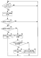
- FIG. 8 is a flowchart relating to frequency adjustment of the clock signal CLK in the configuration shown in FIG. 7 as described above.
- the rising / falling edge detection unit 302 detects the rising edge or the rising edge of the input clock signal CLKIN in step S1 of FIG. 8 (YES in step S1), the process proceeds to step S2.
- step S2 the controller 303 compares the counter value of the 8-bit counter 308 with the expected value.
- the process returns to the determination in step S1. If the difference between the counter value and the expected value is not equal to or less than the first predetermined value in step S3 (NO in step S3), the process proceeds to step S4.
- step S4 if the difference between the counter value and the expected value is not equal to or less than the second predetermined value (> first predetermined value) (NO in step S4), the controller 303 proceeds to step S5. In step S5, the controller 303 updates the value of the coarse adjustment command COARS. On the other hand, if the difference between the counter value and the expected value is equal to or less than the second predetermined value (YES in step S4), the process proceeds to step S6. In step S6, the controller 303 calculates the update value of the fine adjustment command FINE. Then, in step S7, it is determined whether the update value of the fine adjustment command FINE is the maximum value or the minimum value.
- step S7 If the update value is neither the maximum value nor the minimum value (NO in step S7), the process proceeds to step S8, and the controller 303 updates the value of the fine adjustment command FINE to the update value. On the other hand, if the update value is the maximum value or the minimum value (YES in step S7), the process proceeds to step S9, and the controller 303 centers the value of the fine adjustment command FINE while updating the value of the coarse adjustment command COARS. Let it be a value.
- LED drive device 30 semiconductor device
- a wafer test and a final test are performed as inspections before product shipment.
- the wafer test is a test performed before the circuit formed on the wafer is individualized into an IC chip.
- the frequency measurement of the clock signal CLK at the frequency center value setting, the frequency measurement of the clock signal CLK at the frequency maximum value setting, and the frequency minimum value setting are performed by the code setting by the coarse adjustment command COARS and the fine adjustment command FINE.
- the frequency of the clock signal CLK is measured in. The frequency measurement is performed, for example, by bringing the probe into contact with the electrode pad.
- a stack defect test of the mirror capacitance adjusting unit 241 is performed by the first self-diagnosis unit 311 described later. Since the stack defect test can be performed in a short time, it is preferable to include it in the wafer test.
- the final test is a test in the product state after packaging the IC chip, and like the wafer test, the frequency of the clock signal CLK is measured at each setting of the frequency center value, the maximum value, and the minimum value.
- a frequency linearity test between codes is performed by the second self-diagnosis unit 312 (FIG. 7) described later. It is also possible to include the linearity test by the second self-diagnosis unit 312 in the wafer test.
- the first self-diagnosis unit 311 and the second self-diagnosis unit 312 are circuits using BIST (Built-in Self Test).
- BIST is one of the design for testability (DFT) technologies.
- DFT design for testability
- the function of the IC tester is incorporated in the IC chip. Specifically, a "circuit that generates a test pattern" and a “circuit that collates the test result with the expected value" are integrated in the IC.
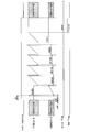
- FIG. 9 is a block diagram showing a configuration related to the test by the first self-diagnosis unit 311.
- FIG. 11 is a diagram showing an example of the internal configuration of the mirror capacitance adjusting unit 241.
- the mirror capacitance adjusting unit 241 has 16 capacitance units CU (1) to CU (16) and 15 capacitance units CU (17) to CU (31).
- the capacity units CU (1) to CU (16) are connected to the node Q1 (FIG. 7).
- the capacity units CU (17) to CU (31) are connected to the node Q2 (FIG. 7).
- FIG. 12 is a diagram showing an example of internal configuration of each capacity unit CU (*).
- the capacity unit CU (*) has a switch SW, a buffer BF, and a capacity C.
- the switch SW switches between conduction and interruption between node Q1 or node Q2 and one end of the capacitance C.
- the first self-diagnosis unit 311 converts the fine adjustment command FINE (5 bits) from the controller 303 into the setting signal DSET (31 bits).
- the on / off of the switch SW in each capacitance unit CU (*) is set according to the setting signal DSET. More specifically, for example, the capacitance units CU (1) to CU (16) in which the "1" and "0" of each bit from the least significant bit to the 16th bit of the setting signal DSET are connected to the node Q1, respectively.
- the setting signal DSET indicates that the switch SW of all the capacitance units CU (*) is off, and the fine adjustment command FINE is "1" (1) (.
- the setting signal DSET indicates that the switch SW of only the capacitance unit CU (1) is on, the switch SW of the remaining capacitance CU (*) is off, and the fine adjustment command FINE is "2" (.
- the setting signal DSET indicates that the switch SW of only the capacitance units CU (1) and CU (2) is on, and the switch SW of the remaining capacitance CU (*) is off. Every time the value (decimal number) of the fine adjustment command FINE is increased by 1, the capacity unit CU (*) in which the switch SW is turned on can be increased by one.
- the number of capacities C connected to the nodes Q1 and Q2 increases as the value of the fine adjustment command FINE increases. This makes it possible to adjust the mirror capacitance.
- FIG. 10 is a timing chart showing an example of a test operation by the first self-diagnosis unit 311.
- the fine adjustment command FINE is set to “0” at the start of the test, and the fixed command TCONT_IH output from the controller 303 is set to Low.
- the first self-diagnosis unit 311 converts the fixed command TCONT_IH into a fixed signal FIX, and instructs the selector 24F to select the fixed signal FIX from the output of the AND circuit 24E and the fixed signal FIX (FIG. FIG. 7).
- the fixed signal FIX is set to High, so the node Q1 is set to Low and the node Q2 is set to High.
- the fixed signal FIX is set to Low, so that the node Q1 is set to High and the node Q2 is set to Low.
- node Q1 is set to Low and node Q2 is set to High.
- the switches SW of all the capacitance units CU (*) are turned off.
- the output signal TIN formed based on the level of the signal output from the buffer BF in each capacitance unit CU (*) is output from the ring oscillator 24 (FIG. 9).
- the output signal TIN is 31-bit data corresponding to the number of capacitance units CU (*).
- the bit data of the output signal TIN is "1"
- the bit data of the output signal TIN is It is set to "0".
- the first self-diagnosis unit 311 compares the output signal TIN with the expected value after a predetermined time has elapsed from the start of the test in consideration of the time from the start of the test until the output signal TIN stabilizes.
- the first self-diagnosis unit 311 considers that there is no abnormality when the output signal TIN matches the expected value, outputs a judgment signal TOUT indicating normality to the controller 303, and when the output signal TIN does not match the expected value, there is an abnormality. Assuming that it has occurred, a determination signal TOUT indicating an abnormality is output to the controller 303.
- the determination signal TOUT is, for example, Low when it is normal, and High when it is abnormal. In addition, once the determination signal reaches a level indicating an abnormality, the level may be continued thereafter.
- the fine adjustment command FINE is maintained at "0"
- the fixed command TCONT_IH is switched to High
- node Q1 is set to High
- node Q2 is set to Low.
- the first self-diagnosis unit 311 compares the output signal TIN with the expected value and outputs the determination signal TOUT.
- the fine adjustment command FINE is switched to "1"
- the fixed command TCONT_IH is switched to Low
- node Q1 is set to Low
- node Q2 is set to High.
- the switch SW of only the capacitance unit CU (1) is turned on.
- the first self-diagnosis unit 311 compares the output signal TIN with the expected value and outputs the determination signal TOUT.
- the fine adjustment command FINE is maintained at "1"
- the fixed command TCONT_IH is switched to High
- node Q1 is set to High
- node Q2 is set to Low.
- the first self-diagnosis unit 311 compares the output signal TIN with the expected value and outputs the determination signal TOUT.
- the level of the nodes Q1 and Q2 is switched while the fine adjustment command FINE is switched, and the output signal TIN is determined.
- FIG. 13 is a diagram showing a configuration example of the second self-diagnosis unit 312.
- the second self-diagnosis unit 312 has an 11-bit counter 312A, a 13-bit counter 312B, a selector 312C, a previous data storage unit 312D, and a comparison unit 312E.
- the value of the coarse adjustment command COARS is changed by keeping the value of the fine adjustment command FINE output from the controller 303 constant, or the value of the coarse adjustment command COARS is changed.
- the frequency of the clock signal CLK is measured by changing the value of the fine adjustment command FINE as a constant, and the frequency linearity between the codes is confirmed.
- the ring oscillator 24 is in the same state as in normal operation, and the selector 24F selects the output of the AND circuit 24E (FIG. 7).
- FIG. 14 is a timing chart showing an example of a test operation when the fine adjustment command FINE is changed while the coarse adjustment command COARS is constant. As shown in FIG. 14, the value of the fine adjustment command FINE is switched at the timing t10. When the stabilization time Ts required for stabilizing the frequency of the clock signal CLK elapses from the timing t10, the start flag is raised. After that, when the start flag goes down (timing t11), the controller 303 causes the 11-bit counter 312A and the 13-bit counter 312B to start counting.
- the 11-bit counter 312A counts 5 MHz signals.
- the 13-bit counter 312B counts the clock signal CLK.
- the comparison timing signal output from the 11-bit counter 312A rises to High.
- the comparison unit 312E compares the counter value by the 13-bit counter 312B at that time with the counter value stored in the previous data storage unit 312D.
- the time required to count the 5 MHz signal for 11 bits is 409.6 ⁇ s, and the frequency of the clock signal CLK is specified by the counter value counted by the 13-bit counter 312B during the time. That is, the 13-bit counter 312B corresponds to a measuring unit that measures the frequency of the clock signal CLK.
- the counter value in the fine adjustment command FINE before the value of the fine adjustment command FINE is switched at the timing t10 is saved in the previous data storage unit 312D, and the counter value is compared by the comparison unit to clock the clocks between the codes. The change in the frequency of the signal CLK can be determined.
- the comparison unit 312E since there is no abnormality in the change in the frequency of the clock signal CLK by the comparison by the comparison unit 312E, the comparison unit 312E notifies the controller 303 that it is normal, and the controller 303 indicates Low. Error flag is output.
- the selector 312C selects the counter value of the 13-bit counter 312B and overwrites the previous data storage unit 312D (previous data update). After that, since the selector 312C selects the output of the previous data storage unit 312D, the data of the previous data storage unit 312D does not change.
- FIG. 16 is a timing chart showing an example of the change pattern of the code (fine adjustment command FINE, coarse adjustment command COARS) in the test using the second self-diagnosis unit 312.
- the normal operation is switched to the test operation, the value of the fine adjustment command FINE is set to "10000", and the coarse adjustment command COARS is set to "0000".
- the stabilization time Ts elapses from the timing t20, counting by the 11-bit counter 312A and the 13-bit counter 312B is started, and the counter value is stored in the previous data storage unit 312D.
- the comparison by the comparison unit 312E is not performed.
- the coarse adjustment command COARS is switched to "00001" while maintaining the value of the fine adjustment command FINE.
- counting by the 11-bit counter 312A and the 13-bit counter 312B is started at the timing when the stabilization time Ts has elapsed from the timing when the coarse adjustment command COARS is switched.
- the new counter value by the 13-bit counter 312B is compared with the counter value of the previous data storage unit 312D. At this time, the new counter value is overwritten and saved in the previous data storage unit 312D.
- the value of the coarse adjustment command COARS is sequentially switched to "11111" to compare the counter values.
- the value of the fine adjustment command FINE is switched to "00001" while maintaining the value of the coarse adjustment command COARS.
- counting by the 11-bit counter 312A and the 13-bit counter 312B is started at the timing when the stabilization time Ts elapses from the timing when the value of the fine adjustment command FINE is switched.
- the new counter value by the 13-bit counter 312B is compared with the counter value of the previous data storage unit 312D. At this time, the new counter value is overwritten and saved in the previous data storage unit 312D.
- the value of the fine adjustment command FINE is sequentially switched to "11111" to compare the counter values.
- the value of the fine adjustment command FINE is switched to "11111"
- the value of the fine adjustment command FINE is switched to "00000”
- the value of the coarse adjustment command COARS is switched to "00110".
- the comparison is not performed by the comparison unit 312E, and the counter value is stored in the previous data storage unit 312D.
- the value of the fine adjustment command FINE is sequentially switched to "11111" to compare the counter values.
- the value of the coarse adjustment command COARS is switched in the order of "01100”, “10000”, “10110”, “11100”, “11111”, and the fine adjustment command FINE is performed while the value of the coarse adjustment command COARS is constant.
- the counter values are compared while switching the value of.
- the LED drive device 30 shown in FIG. 1 is a packaged product having a rectangular shape when viewed from above. Of the two opposite sides of the rectangular shape, the PWMIN terminal is arranged on one side, and the PWMOUT terminal is arranged on the other side.
- the PWM OUT terminal is arranged on the same side as the side on which the FBV terminal is arranged, it is desirable that at least one terminal is arranged between the PWM OUT terminal and the FBV terminal.
- the PWMOUT terminal is arranged on the same side as the side on which the MINSELV terminal is arranged, it is desirable that at least one terminal is arranged between the PWMOUT terminal and the MINSELV terminal. That is, it is desirable that the PWMOUT terminal is not adjacent to the FBV terminal and the MINSELV terminal. This is because the signal generated at the PWM OUT terminal is a rectangular wave, whereas the signal generated at the FBV terminal and the MINSELV terminal is an analog signal.
- the PWM OUT terminal is a low withstand voltage terminal
- the PGND terminal, SW terminal, GH terminal, BOOT terminal, VIN terminal, SNSP terminal, SNSN terminal, and COMP terminal are high withstand voltage terminals, which may cause a short circuit between the terminals.
- the PWMOUT terminal is arranged on the same side as the side on which any of the LED terminals 1 to LED24 (for example, LED13 to LED24 terminals) is arranged, at least one terminal is connected to the LED terminal. Is desirable to be placed. That is, it is desirable that the PWM OUT terminal is not adjacent to the LED terminal. This is because a high voltage is applied to the LED terminal.
- the present invention can be used as an example for driving a vehicle-mounted LED.
Landscapes
- Engineering & Computer Science (AREA)
- Theoretical Computer Science (AREA)
- Physics & Mathematics (AREA)
- General Engineering & Computer Science (AREA)
- General Physics & Mathematics (AREA)
- Mathematical Physics (AREA)
- Computer Hardware Design (AREA)
- Led Devices (AREA)
Abstract
第1クロック信号を生成する発振器と、外部から入力クロック信号を入力される第1端子と、前記入力クロック信号のエッジ間において、前記第1クロック信号に基づくクロック信号をカウントする第1カウンタと、前記第1カウンタによるカウンタ値と期待値との比較結果に基づき、前記第1クロック信号の周波数を調整する指令を前記発振器に送るコントローラと、を有する半導体装置としている。
Description
本発明は、発振器を有する半導体装置に関する。
従来、半導体集積回路(IC)を含んで形成される半導体装置には、クロック信号を生成する発振器が備えられる場合が多い。例えば、クロック信号に基づきPWM(Pulse Width Modulation)信号を生成することができる。
そして、上記半導体装置が例えばLED(Light Emitting Diode)駆動装置(LEDドライバ)である場合、上記PWM信号を用いてLEDのPWM調光を行うLED駆動装置が存在する。なお、PWM調光機能を有するLED駆動装置の一例は、特許文献1に開示されている。
ここで、例えばアプリケーションとしてLEDの灯数が多く必要な場合等により、複数の上記半導体装置を用いてシステムを構成する場合がある。この場合、個々の半導体装置に含まれる発振器により生成されるクロック信号の周波数にばらつきが存在する虞がある。クロック信号の周波数にばらつきが存在すると、例えばPWM信号の同期がとれないことが生じうる。この場合、例えば、LEDのPWM調光により形成される画像に不具合が生じる虞がある。
なお、個々の半導体装置に含まれる発振器を水晶発振器とすれば、クロック信号の周波数のばらつきを抑えることは可能であるが、コスト面で不利である。
上記状況に鑑み、本発明は、複数の半導体装置を用いる場合でも、個々の半導体装置において生成されるクロック信号の周波数の同期を可能とする半導体装置を提供することを目的とする。
本発明の一態様に係る半導体装置は、
第1クロック信号を生成する発振器と、
外部から入力クロック信号を入力される第1端子と、
前記入力クロック信号のエッジ間において、前記第1クロック信号に基づくクロック信号をカウントする第1カウンタと、
前記第1カウンタによるカウンタ値と期待値との比較結果に基づき、前記第1クロック信号の周波数を調整する指令を前記発振器に送るコントローラと、
を有する構成としている(第1の構成)。
第1クロック信号を生成する発振器と、
外部から入力クロック信号を入力される第1端子と、
前記入力クロック信号のエッジ間において、前記第1クロック信号に基づくクロック信号をカウントする第1カウンタと、
前記第1カウンタによるカウンタ値と期待値との比較結果に基づき、前記第1クロック信号の周波数を調整する指令を前記発振器に送るコントローラと、
を有する構成としている(第1の構成)。
また、上記第1の構成において、前記第1クロック信号を所定の分周比で分周して第2クロック信号を生成する分周部と、前記入力クロック信号と前記第2クロック信号のうちいずれかを選択して出力クロック信号として出力するセレクタと、前記出力クロック信号を外部へ出力させる第2端子と、を有する構成としてもよい(第2の構成)。
また、上記第2の構成において、前記分周部は、前記第1クロック信号を第1分周比で分周する第1分周器と、前記第1分周器の出力を第2分周比で分周する第2分周器と、
を有し、前記第1カウンタは、前記第1分周器の出力をカウントする構成としてもよい(第3の構成)。
を有し、前記第1カウンタは、前記第1分周器の出力をカウントする構成としてもよい(第3の構成)。
また、上記第2または第3の構成において、前記分周部は、デューティが所定値に制約された前記第2クロック信号を生成する構成としてもよい(第4の構成)。
また、上記第2から第4のいずれかの構成において、前記セレクタによる前記入力クロック信号の選択、前記第2クロック信号の選択、前記出力クロック信号を出力しない選択のいずれかを設定可能である構成としてもよい(第5の構成)。
また、上記第1から第5のいずれかの構成において、前記発振器は、リングオシレータである構成としてもよい(第6の構成)。
また、上記第6の構成において、前記リングオシレータは、奇数個のインバータと、前記コントローラからの粗調整指令をDA変換するDAC(DAコンバータ)と、前記DACの出力に応じた電流を前記インバータに流す電流供給部と、前記コントローラからの精調整指令に基づき、前記インバータ間のノードに接続させる容量値を変化させるミラー容量調整部と、を有する構成としてもよい(第7の構成)。
また、上記第7の構成において、前記ミラー容量調整部は、容量と、前記容量と前記ノードとの間に配置されるスイッチと、を含む容量ユニットを複数有しており、当該半導体装置は、前記スイッチをオンとする前記容量ユニットのパターンを変化させつつ、前記ノードにLowとHighの電圧を各々印加させ、前記容量ユニットからの出力を期待値と比較する第1自己診断部をさらに有する構成としてもよい(第8の構成)。
また、上記第7または第8の構成において、前記コントローラが前記粗調整指令と前記精調整指令のうち一方を一定として他方を変化させるテスト動作において、前記第1クロック信号の周波数を測定する測定部と、指令の変化前後における前記測定部による測定結果を比較する比較部と、を含む第2自己診断部をさらに有する構成としてもよい(第9の構成)。
また、上記第9の構成において、前記第2自己診断部は、所定周波数の信号をカウントする所定ビットの第2カウンタを含み、前記測定部は、前記第2カウンタが前記所定ビット分カウントする期間において前記第1クロック信号をカウントする第3カウンタである構成としてもよい(第10の構成)。
また、上記第1から第10のいずれかの構成において、前記第1クロック信号に基づいてPWM信号を生成するPWM信号生成部を有する構成としてもよい(第11の構成)。
また、上記第11の構成において、前記PWM信号生成部は、前記入力クロック信号のエッジが検出されたときに前記PWM信号のエッジを形成させる構成としてもよい(第12の構成)。
また、上記第11または第12の構成において、LEDのカソードを接続可能なLED端子と、前記LED端子に流す電流を制御する電流ドライバと、を有し、前記電流ドライバは、前記PWM信号に応じてオンオフされる構成としてもよい(第13の構成)。
また、本発明の一態様に係る半導体装置システムは、上記第13の構成とした半導体装置を複数含み、複数の前記半導体装置の各々には、外部からCAN(Controller Area Network)トランシーバを介して前記PWM信号のオンデューティが指令される構成としている(第14の構成)。
また、本発明の一態様に係る半導体装置システムは、上記第2から第5のいずれかの構成とした半導体装置を複数含み、前段側の前記半導体装置における前記第2端子と、後段側の前記半導体装置における前記第1端子とが接続される構成としている(第15の構成)。
また、上記第15の構成とした半導体装置システムは、車載用であることとしてもよい。
本発明の半導体装置によると、複数の半導体装置を用いる場合でも、個々の半導体装置において生成されるクロック信号の周波数の同期を可能とする。
以下に本発明の例示的な実施形態について図面を参照して説明する。なお、以下に記載する具体的な数値は、一例である。
<1.LED駆動装置の構成>
図1は、本発明の例示的な実施形態に係るLED駆動装置30の構成を示す図である。図1に示すLED駆動装置30は、複数チャンネル(本実施例では一例として24チャンネル)のLEDアレイA1~A24を駆動する。LED駆動装置30は、一例として、車載用である。
図1は、本発明の例示的な実施形態に係るLED駆動装置30の構成を示す図である。図1に示すLED駆動装置30は、複数チャンネル(本実施例では一例として24チャンネル)のLEDアレイA1~A24を駆動する。LED駆動装置30は、一例として、車載用である。
LED駆動装置30は、最小電圧選択部1と、基準電圧生成部2と、スペクトラム拡散用基準電圧生成部3と、周波数/電圧変換部4と、エラーアンプ5と、リップル注入部6と、アンプ7と、Low側コンパレータ8と、High側コンパレータ9と、RSフリップフロップ10と、OCP(過電流保護)部11と、ドライバロジック部12と、ダイオード13と、ドライバ14と、SWOCP部15と、NMOSトランジスタ16と、UVLO(Under Voltage Lock Out)/TSD(Thermal Shut Down)部17と、バンドギャップリファレンス18と、内部電圧生成部19と、内部電圧生成部20と、異常通知部21と、NMOSトランジスタ22と、I/O(入出力)ポート23と、リングオシレータ24と、制御ロジック部25と、電流ドライバ26と、ショート検出部27と、オープン検出部28と、を集積化した半導体集積回路(ICチップ)を有する半導体装置である。
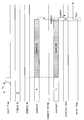
また、LED駆動装置30は、外部との電気的接続を確立するための外部端子として、COMP端子、SNSN端子、SNSP端子、BOOT端子、GH端子、SW端子、PGND端子、VIN端子、VREG5端子、VREG3端子、FAILB端子、EN端子、RX端子、TX端子、CS0~CS3端子、PWMIN端子、FBV端子、MINSELV端子、LED1~LED24端子、LGND1~LGND4端子、PWMOUT端子、および、GND端子を有している。
LED駆動装置30の外部には、入力電圧Vinから出力電圧VoutをDC/DC変換により生成してLEDアレイA1~A24のアノードに供給するための出力段35が配置される。出力段35は、各々ディスクリート部品であり、スイッチング素子N1と、ダイオードD1と、インダクタL1と、抵抗R1と、出力コンデンサCoと、を有する。スイッチング素子N1がLED駆動装置30により駆動制御されることにより、出力段35はLED駆動装置30により制御される。出力段35とLED駆動装置30とにより、DC/DCコンバータが形成される。なお、本実施形態では、特にDC/DCコンバータとして、非同期整流型の降圧DC/DCコンバータが構成される。
より具体的には、NMOSトランジスタにより構成されるスイッチング素子N1のドレインは、入力電圧Vinの印加端に接続される。スイッチング素子N1のソースとダイオードD1のカソードが接続されるノードNd1は、SW端子に接続される。ダイオードD1のアノードは、グランド電位の印加端に接続される。ノードNd1は、インダクタL1の一端に接続される。インダクタL1の他端は、抵抗R1の一端とノードNd2で接続される。抵抗R1の他端は、出力コンデンサCoの一端とノードNd3で接続される。出力コンデンサCoの他端は、グランド電位の印加端に接続される。
スイッチング素子N1のゲートは、GH端子を介してドライバ14の出力端に接続される。ドライバ14の低電位側は、SW端子に接続される。ドライバ14の高電位側は、ダイオード13のカソードに接続される。ダイオード13のアノードは、基準電圧Vdrv5の印加端に接続される。ブート用コンデンサCbの一端は、インダクタL1とノードNd1の間に接続される。ブート用コンデンサCbの他端は、BOOT端子を介してダイオード13のカソードに接続される。
スイッチング素子N1がオンのとき、スイッチング素子N1を通してインダクタL1および抵抗R1に向けて電流が流れる。このとき、ドライバロジック部12の制御によりドライバ14の出力がSW端子電圧(Low)とされると、スイッチング素子N1はオフとされる。これにより、ダイオードD1を通してインダクタL1および抵抗R1に向けて電流が流れる。このとき、ブート用コンデンサCbは、基準電圧Vdrv5によりダイオード13を介して充電される。
そして、ドライバロジック部12の制御によりドライバ14の出力がBOOT端子電圧となると、スイッチング素子N1はオンとなる。このとき、BOOT端子には、入力電圧Vinから充電によりブート用コンデンサCbに生じる電圧だけ高い電圧が生じる。これにより、NMOSトランジスタであるスイッチング素子N1をオンとさせることが可能となる。
このようなスイッチング素子N1のオンオフ制御により、ノードNd3に出力電圧Voutが生成される。
また、LEDアレイA1~A24の各カソードは、それぞれLED1~LED24端子に接続される。最小電圧選択部1は、LED1~LED24端子の各端子電圧(カソード電圧)のうち最小となる電圧を選択する。
一方、抵抗R1の一端が接続されるノードNd2は、SNSP端子に接続される。抵抗R1の他端が接続されるノードNd3は、SNSN端子に接続される。SNSP端子電圧およびSNSN端子電圧は、アンプ7に入力される。アンプ7は、SNSP端子電圧とSNSN端子電圧の電圧差を増幅して出力する。これにより、アンプ7は、インダクタL1(抵抗R1)に流れるインダクタ電流を検出する。
リップル注入部6は、アンプ7の出力に基づき、最小電圧選択部1により選択された最小電圧にリップルを注入する。リップルを注入後の最小電圧は、Low側コンパレータ8の反転入力端(-)に入力されるとともに、High側コンパレータ9の非反転入力端(+)に入力される。Low側コンパレータ8の出力は、RSフリップフロップ10のリセット端子に入力される。High側コンパレータ9の出力は、RSフリップフロップ10のセット端子に入力される。RSフリップフロップ10のQ出力端子からは、フリップフロップ出力信号FFOUTが出力される。ドライバロジック部12は、フリップフロップ出力信号FFOUTに基づきドライバ14を介してスイッチング素子N1を制御する。
周波数/電圧変換部4は、フリップフロップ出力信号FFOUTの周波数を電圧信号に変換してエラーアンプ5の非反転入力端(+)に出力する。一方、エラーアンプ5の反転入力端(-)には、スペクトラム拡散用基準電圧生成部3の出力が入力される。基準電圧生成部2は、エラーアンプ5の出力に基づき、Low側基準電圧VrefLおよびHigh側基準電圧VrefHを可変に生成する。Low側基準電圧VrefLは、Low側コンパレータ8の非反転入力端(+)に入力される。High側基準電圧VrefHは、High側コンパレータ9の反転入力端(-)に入力される。
このような構成により、ヒステリシス制御(Bang-Bang制御)が行われ、LEDアレイA1~LEDアレイA24のカソード電圧のうち最小の電圧が所望の電圧に制御される。また、スペクトラム拡散用基準電圧生成部3によってスイッチング周波数が時間的に変化することにより、スペクトラムの周波数を分散させてスペクトラムのパワーのピークを抑制し、EMI(Electro Magnetic Interference)対策を行うことができる。
なお、FBV端子およびMINSELV端子は、LED駆動装置30を複数接続して使用する場合に用いる。ここで、図2Aに、一例として、LED駆動装置30(30m,30s1,30s2)を3つ接続して使用する場合の構成を示す。図2Aにおいて、LED駆動装置30mが後述するマスタに相当し、LED駆動装置30s1,30s2が後述するスレーブに相当する。
LED駆動装置30m,30s1,30s2のそれぞれには、LEDアレイA1~A24の各カソードが接続される。LEDアレイA1~A24の各アノードには、LED駆動装置30mにおけるDC/DC機能により生成される出力電圧Voutが印加される。LED駆動装置30s1,30s2では、DC/DC機能は使用されない。なお、図2Aでは、出力電圧Voutの出力に関する構成は便宜上、簡略化して図示している。
FBV端子は、LEDアレイA1~A24の各カソード電圧と、MINSELV端子の電圧のうち最小選択部1により選択された最小の電圧を出力する。MINSELV端子には、外部のLED駆動装置30のFBV端子が接続される。
図2Aの例であれば、LED駆動装置30mのMINSELV端子は、LED駆動装置30s1のFBV端子に接続され、LED駆動装置30s1のMINSELV端子は、LED駆動装置30s2のFBV端子に接続される。LED駆動装置30mのFBV端子およびLED駆動装置30s2のMINSELV端子は非接続である。なお、LED駆動装置30s2のMINSELV端子は、最小電圧の選択に影響を与えないように、例えばLED駆動装置30s2におけるVREG5端子に生じる基準電圧Vdrv5のようなゲインの高い電圧の印加端に接続することが望ましい。
これにより、LED駆動装置30s2では、LEDアレイA1~A24の各カソード電圧のうち最小の電圧が選択され、選択された最小電圧が自身のFBV端子より出力される。LED駆動装置30s1では、自身のMINSELV端子にLED駆動装置30s2のFBV端子から入力される電圧と、LEDアレイA1~A24の各カソード電圧のうち最小の電圧が選択され、選択された最小電圧が自身のFBV端子より出力される。LED駆動装置30mでは、自身のMINSELV端子にLED駆動装置30s1のFBV端子から入力される電圧と、LEDアレイA1~A24の各カソード電圧のうち最小の電圧が選択され、選択された最小電圧がDC/DC機能に使用される。
従って、複数接続されたLED駆動装置30に接続されるすべてのLEDアレイ(図2Aの場合は24チャンネル×3=72チャンネル)の各カソード電圧のうち最小の電圧が所望値となるよう出力電圧Voutが制御される。
図1に説明を戻し、OCP部11は、アンプ7によるインダクタ電流の検出結果に基づき過電流を検出し、保護を行う。
SWOCP部15は、スイッチング素子N1に流れる過電流を検出する回路である。
NMOSトランジスタ16は、SW端子とPGND端子との間に接続される。PGND端子は、グランド電位に接続される。ドライバロジック部12によりNMOSトランジスタ16がオンされることで、出力コンデンサCoの放電が行われる。
UVLO/TSD部17は、入力電圧Vinを監視して低電圧保護を行うとともに、LED駆動装置30のジャンクション温度を監視して過熱保護を行う。
入力電圧Vinは、バッテリ電源Bに基づき生成され、VIN端子に印加される。バンドギャップリファレンス18は、VIN端子に印加される入力電圧Vinに基づき安定した基準電圧Vbgを生成する基準電圧源である。内部電圧生成部19は、入力電圧Vinに基づき5Vの基準電圧Vdrv5を生成する。内部電圧生成部19の出力端は、VREG5端子を介してコンデンサに接続される。内部電圧生成部20は、基準電圧Vdrv5に基づき3.3Vの基準電圧Vref33を生成する。内部電圧生成部20の出力端は、VREG3端子を介してコンデンサに接続される。
MCU(Micro Controller Unit)45およびCAN(Controller Area Network)トランシーバ40は、LED駆動装置30の外部に配置される。
NMOSトランジスタ22は、VREG3端子に生じる基準電圧Vref33に抵抗によりプルアップされる。異常通知部21は、制御ロジック部25からの指令に基づきNMOSトランジスタ22をオンさせることで、異常を示すLowの異常信号faultをMCU45に通知する。
MCU45は、EN端子およびI/Oポート23を介して制御ロジック部25にイネーブル信号enableを送信する。
CANトランシーバ40は、MCU45からCANバスCBを介して受信したデータを受信データRxdとしてRX端子に送信する。制御ロジック部25は、受信データRxdをI/Oポート23を介して受信する。制御ロジック部25は、I/Oポート23を介して送信データTxdをTX端子に送信する。CANトランシーバ40は、TX端子から受信した送信データTxdをCANバスCBを介してMCU45に送信する。なお、I/Oポート23は、UART(Universal Asynchronous Receiver/Transmitter)として構成され、シリアル信号とパラレル信号との間の変換を行う。
CS0~CS3端子は、それぞれ電源電圧に抵抗によりプルアップされる。CS0~CS3端子に設定されるHighまたはLowの組み合わせにより、LED駆動装置30を識別するための固有番号(ID)が制御ロジック部25に設定される。
リングオシレータ24は、クロック信号を生成する発振器である。当該クロック信号に基づいてPWM信号が生成され、PWM調光が行われる。
PWMIN端子、PWMOUT端子、およびセレクタ301は、後述のようにLED駆動装置30を複数接続して、個々のLED駆動装置30におけるリングオシレータ24により生成されるクロック信号の周波数を同期させる場合に用いられ、その詳細については後に述べる(なお、図1では、リングオシレータ24とセレクタ301との接続関係は簡略化して記載している)。
電流ドライバ26は、LED1端子~LED24端子それぞれに対応して設けられ、LEDアレイA1~A24のそれぞれに定電流を流す。PWM信号に基づいて電流ドライバ26のオンオフが制御されることで、LEDアレイA1~A24のPWM調光が行われる。また、電流ドライバ26をオン状態としたうえで定電流の設定値を可変とすることで調光を行うDC調光も可能としている。
ショート検出部27は、LED1端子~LED24端子それぞれに対応して設けられ、当該端子の電圧に基づいてLEDアレイA1~A24のショートを検出し、ショート保護を行う。
オープン検出部28は、LED1端子~LED24端子それぞれに対応して設けられ、当該端子の電圧に基づいてLEDアレイA1~A24のオープンを検出し、オープン保護を行う。
<2.LED駆動装置の複数接続について>
本実施形態では、LEDの灯数を多く必要なアプリケーションに対応して、LED駆動装置30(半導体装置)を複数接続することが可能となっている。図2Bは、アプリケーションの一例として、車両のリアランプにLED駆動装置30を適用した場合のシステム構成例を示す。なお、図2Bにおいて、便宜上、個々のLED駆動装置30をそれぞれ30A~30Hの符号で示している。また、図2BにおけるCANトランシーバ40A~40Cは、図1に示すCANトランシーバ40に相当する。
本実施形態では、LEDの灯数を多く必要なアプリケーションに対応して、LED駆動装置30(半導体装置)を複数接続することが可能となっている。図2Bは、アプリケーションの一例として、車両のリアランプにLED駆動装置30を適用した場合のシステム構成例を示す。なお、図2Bにおいて、便宜上、個々のLED駆動装置30をそれぞれ30A~30Hの符号で示している。また、図2BにおけるCANトランシーバ40A~40Cは、図1に示すCANトランシーバ40に相当する。
図2Bに示すように、車両後部左側のリアランプにLED駆動装置30A,30BおよびCANトランシーバ40Aが適用されている。LED駆動装置30A,30BおよびCANトランシーバ40Aは、プリント基板P1に実装されている。LED駆動装置30Aと30Bとを接続することで半導体装置システム300Aが構成される。
車両後部左側のリアランプでは、LED駆動装置30A,30Bにより24チャンネル×2=48チャンネルのLEDアレイが駆動される。前段側のLED駆動装置30AのPWMOUT端子が、後段側のLED駆動装置30BのPWMIN端子に接続される。これにより、LED駆動装置30Aをマスタ、LED駆動装置30Bをスレーブとして、LED駆動装置30Aのリングオシレータ24Aにより生成されるクロック信号の周波数に、LED駆動装置30Bのリングオシレータ24Bにより生成されるクロック信号の周波数を同期させることが可能となる。なお、周波数を同期させる方法については、後述する。
また、図2Bに示すように、車両後部中央のリアランプにLED駆動装置30C~30FおよびCANトランシーバ40Bが適用されている。LED駆動装置30C~30FおよびCANトランシーバ40Bは、プリント基板P2に実装されている。LED駆動装置30C~30Fを接続することで半導体装置システム300Bが構成される。
車両後部中央のリアランプでは、LED駆動装置30C~30Fにより24チャンネル×4=96チャンネルのLEDアレイが駆動される。前段側のLED駆動装置30CのPWMOUT端子が、後段側のLED駆動装置30DのPWMIN端子に接続される。前段側のLED駆動装置30DのPWMOUT端子が、後段側のLED駆動装置30EのPWMIN端子に接続される。前段側のLED駆動装置30EのPWMOUT端子が、後段側のLED駆動装置30FのPWMIN端子に接続される。これにより、LED駆動装置30Cをマスタ、LED駆動装置30D~30Fをスレーブとして、LED駆動装置30Cのリングオシレータ24Cにより生成されるクロック信号の周波数に、LED駆動装置30D~30Fのリングオシレータ24D~24Fにより生成されるクロック信号の周波数を同期させることが可能となる。
図2Bに示すように、車両後部右側のリアランプにLED駆動装置30G,30HおよびCANトランシーバ40Cが適用されている。LED駆動装置30G,30HおよびCANトランシーバ40Cは、プリント基板P3に実装されている。LED駆動装置30Gと30Hとを接続することで半導体装置システム300Cが構成される。
車両後部右側のリアランプでは、LED駆動装置30G,30Hにより24チャンネル×2=48チャンネルのLEDアレイが駆動される。前段側のLED駆動装置30GのPWMOUT端子が、後段側のLED駆動装置30HのPWMIN端子に接続される。これにより、LED駆動装置30Gをマスタ、LED駆動装置30Hをスレーブとして、LED駆動装置30Gのリングオシレータ24Gにより生成されるクロック信号の周波数に、LED駆動装置30Hのリングオシレータ24Hにより生成されるクロック信号の周波数を同期させることが可能となる。
また、LED駆動装置30A,30BとCANトランシーバ40Aとの間でデータの送受信が可能である。LED駆動装置30C~30FとCANトランシーバ40Bとの間でデータの送受信が可能である。LED駆動装置30G,30HとCANトランシーバ40Cとの間でデータの送受信が可能である。
CANトランシーバ40A~40Cは、プリント基板P4に実装されたMCU45との間でワイヤハーネス50を介してデータの送受信が可能である。CANバスCB(図1)は、ワイヤハーネス50に含まれる。MCU45は、CANトランシーバ40A~40Cを介してLED駆動装置30A~30HにPWM調光のオンデューティを指令することができる。
また、MCU45は、ワイヤハーネス50を介してLED駆動装置30A~30Hにイネーブル信号enableを送信可能であるとともに、ワイヤハーネス50を介してLED駆動装置30A~30Hから異常信号faultを受信可能である。
<3.クロック信号の周波数同期>
次に、リングオシレータ24により生成されるクロック信号の周波数の同期方法について説明する。図3は、LED駆動装置30におけるクロック信号の周波数同期に関する構成を示すブロック図である。なお、図3には、PWM調光に関する構成もあわせて示す。
次に、リングオシレータ24により生成されるクロック信号の周波数の同期方法について説明する。図3は、LED駆動装置30におけるクロック信号の周波数同期に関する構成を示すブロック図である。なお、図3には、PWM調光に関する構成もあわせて示す。
図3に示すように、LED駆動装置30は、セレクタ301と、立上げ/立下げエッジ検出部302と、コントローラ303と、分周器304と、PWM信号生成部305と、レジスタ306と、分周器307と、8ビットカウンタ308と、レジスタ309と、を有している。
立上げ/立下げエッジ検出部302は、外部からPWMIN端子へ入力される入力クロック信号CLKINの立上げエッジおよび立下げエッジを検出する。
コントローラ303は、粗調整指令COARSおよび精調整指令FINEをリングオシレータ24に送信することで、リングオシレータ24の生成するクロック信号CLKの周波数を調整する。なお、ここでは、粗調整指令COARSおよび精調整指令FINEともに、一例として5ビットのデジタル指令信号であるとする。なお、このような指令により周波数を調整する構成については、後述する。
また、リングオシレータ24の生成するクロック信号CLKの周波数は、一例として、ティピカル値として18MHzであるとする。分周器304は、クロック信号CLKの周波数を所定の分周比にて分周する。ここでは、所定の分周比は、一例として1/144であるとする。これにより、分周器304から出力される分周後のクロック信号CLKd1は、ティピカル値として、18MHz/144=125kHzとなる。
PWM信号生成部305は、クロック信号CLKd1に基づいてPWM信号pwmsを生成する。例えば、PWM信号生成部305は、クロック信号CLKd1をカウントするカウンタを有する。そして、スレーブのLED駆動装置30においては、PWM信号生成部305は、立上げ/立下げエッジ検出部302により入力クロック信号CLKINの立上げエッジが検出されたときにPWM信号pwmsをHighに立上げ、そのときに上記カウンタをリセットする。そして、後述する分周器307の分周比における分子を1とした分母の整数に対して、レジスタ306に設定されたPWM調光のオンデューティを乗算したカウント値を上記カウンタがカウントしたときに、PWM信号生成部305はPWM信号pwmsをLowへ立下げる。後述のように、分周器307の分周比は一例として1/256であるので、オンデューティが例えば50%の場合、256×50%=128が上記カウント値となる。
なお、上記に限らず、PWM信号生成部305は、例えば、カウンタが分周器307の分周比における分子を1とした分母の整数をカウントしたときにPWM信号pwmsをHighに立ち上げるとともにカウンタをリセットしてもよい。
ただし、マスタのLED駆動装置30においては、PWM信号生成部305は、分周器307によるクロック信号CLKd2のHighへの立上げと同時にカウンタをリセットしてPWM信号pwmsをHighに立上げ、オンデューティに応じたカウンタ値をカウントしたときにPWM信号pwmsをLowに立下げて、PWM信号pwmsを生成する。
なお、MCU45からCANトランシーバ40を介した指令により、レジスタ306にはPWM調光のオンデューティが設定される。
図3に示すように、電流ドライバ26は、NMOSトランジスタ26Aと、抵抗26Bと、エラーアンプ26Cと、スイッチ26Dと、を有する。NMOSトランジスタ26Aのドレインは、LED1~LED24端子のいずれかに接続される。NMOSトランジスタ26Aのソースは、抵抗26Bの一端に接続される。抵抗26Bの他端は、グランド電位の印加端に接続される。NMOSトランジスタ26Aのソースと抵抗26Bとが接続されるノードは、エラーアンプ26Cの反転入力端(-)に接続される。エラーアンプ26Cの非反転入力端(+)には、所定の基準電圧が印加される。スイッチ26Dは、エラーアンプ26Cの出力端とNMOSトランジスタ26Aのゲートとの間に配置される。
PWM信号pwmsの1周期におけるオンデューティ期間においてスイッチ26Dがオンとされることで電流ドライバ26がオンとされ、オフデューティ期間においてスイッチ26Dがオフとされることで電流ドライバ26がオフとされる。これにより、PWM信号pwmsに応じたPWM調光が行われる。
また、レジスタ306には、PWM信号pmwsのLEDチャンネル間の遅れ量も設定可能である。これにより、全チャンネルのLEDアレイに同時に電流が流れ始めることを抑制できる。
また、分周器307は、クロック信号CLKd1を所定の分周比で分周する。ここで、所定の分周比は、一例として1/256であるとする。これにより、分周器307から出力される分周後のクロック信号CLKd2は、ティピカル値として125kHz/256=488Hzとなる。ただし、分周器307は、所定のデューティのクロック信号CLKd2を生成する。ここでは、所定のデューティは、一例として50%とする。
セレクタ301は、レジスタ309での設定に応じて、PWMIN端子からの入力クロック信号CLKINと、分周器307からのクロック信号CLKd2のうちいずれかを選択して出力クロック信号CLKOUTとしてPWMOUT端子を介して外部へ出力するか、または、出力クロック信号CLKOUTを出力させない。
ここで、図4は、レジスタ309に設定される2ビットの設定データSYNCSETと、PWMIN端子の有効/無効、PWMOUT端子の有効/無効の対応関係を示す。
図4に示すように、SYNCSET=“01”に設定された場合、セレクタ301は、クロック信号CLKd2(ティピカル値=18KHz/(144×256)=488Hz)を選択して出力クロック信号CLKOUTとして出力し、SYNCSET=“11”に設定された場合、セレクタ301は、入力クロック信号CLKINを選択して出力クロック信号CLKOUTとして出力する。なお、SYNCSET=“00”または“10”に設定された場合、セレクタ301は、出力クロック信号CLKOUTを出力させず、PWMOUT端子は無効(disable)となる。
また、図4に示すように、SYNCSET=“10”または“11”に設定された場合、コントローラ303は、入力クロック信号CLKINに基づくクロック信号CLKの周波数調整を行う。すなわち、PWMIN端子は、有効(enable)となる。
より具体的には、立上げ/立下げエッジ検出部302により入力クロック信号CLKINの立上げエッジが検出されたときに、コントローラ303は、8ビットカウンタ308をリセットする。8ビットカウンタ308は、クロック信号CLKd1をカウントする。そして、立上げ/立下げエッジ検出部302により入力クロック信号CLKINの立下げエッジが検出されたとき、コントローラ303は、8ビットカウンタ308のカウンタ値を所定の第1期待値と比較する。ここで、第1期待値は、例えば、分周器307の分周比における分子を1とした分母の整数に、クロック信号CLKd2のデューティを乗算した値である。すなわち、第1期待値は、一例として、256×50%=128となる。
コントローラ303は、カウンタ値が第1期待値より大きい場合、リングオシレータ24にクロック信号CLKの周波数を低くするように指令し、カウンタ値が第1期待値より小さい場合、リングオシレータ24にクロック信号CLKの周波数を高くするように指令する。
また、立上げ/立下げエッジ検出部302により入力クロック信号CLKINの立下げエッジが検出されたとき、コントローラ303は、8ビットカウンタ308をリセットする。その後、立上げ/立下げエッジ検出部302により入力クロック信号CLKINの立上げエッジが検出されたとき、コントローラ303は、8ビットカウンタ308のカウンタ値を所定の第2期待値と比較する。ここで、第2期待値は、例えば、分周器307の分周比における分子を1とした分母の整数から、上記第1期待値を減算した値である。すなわち、第1期待値が128である場合、第2期待値は、256-128=128である。
コントローラ303は、カウンタ値が第2期待値より大きい場合、リングオシレータ24にクロック信号CLKの周波数を低くするように指令し、カウンタ値が第2期待値より小さい場合、リングオシレータ24にクロック信号CLKの周波数を高くするように指令する。
なお、入力クロック信号CLKINの立下げエッジが検出されたときにカウンタはリセットせずにカウントを継続し、その後、入力クロック信号CLKINの立上げエッジが検出されたときに、カウンタ値を第2期待値と比較してもよい。この場合、第2期待値は、上記の例では256となる。
また、分周器304は必須ではなく、カウンタ(8ビットカウンタ308に相当)がクロック信号CLKを直接カウントしてもよい。
なお、図4に示すように、SYNCSET=“00”または“01”に設定された場合、コントローラ303による入力クロック信号CLKINに基づくクロック信号CLKの周波数調整は行われず、PWMIN端子は無効(disable)となる。
ここで、図5は、一例として、先述した図2Bに示すようなLED駆動装置30C~30Fを接続して半導体装置システム300Bを構成した場合の、個々のLED駆動装置30のレジスタ309に設定されるSYNCSETを示している。
マスタであるLED駆動装置30Cでは、SYNCSET=“01”に設定される。これにより、PWMIN端子は無効となり、リングオシレータ24は、コントローラ303から指令されるコードに応じた周波数のクロック信号CLKを生成し、生成されたクロック信号CLKは、分周器304および分周器307により分周され、分周後のクロック信号CLKd2がセレクタ301により選択されて出力クロック信号CLKOUTとしてPWMOUT端子から外部へ出力される。
スレーブであるLED駆動装置30Dでは、SYNCSET=“11”に設定される。これにより、PWMIN端子が有効となり、先述したコントローラ303による入力クロック信号CLKINに基づくクロック信号CLKの周波数調整が行われる。ここで、入力クロック信号CLKINは、前段のLED駆動装置30CのPWMOUT端子から出力される出力クロック信号CLKOUTである。これにより、スレーブであるLED駆動装置30Dのリングオシレータ24により生成されるクロック信号CLKの周波数は、マスタであるLED駆動装置30Cのリングオシレータ24により生成されるクロック信号CLKの周波数と一致するように調整される。
また、LED駆動装置30Dでは、セレクタ301により入力クロック信号CLKINが選択されて出力クロック信号CLKOUTとしてPWMOUT端子から外部へ出力される。
スレーブであるLED駆動装置30Eでは、SYNCSET=“11”に設定される。これにより、PWMIN端子が有効となり、先述したコントローラ303による入力クロック信号CLKINに基づくクロック信号CLKの周波数調整が行われる。ここで、入力クロック信号CLKINは、前段のLED駆動装置30DのPWMOUT端子から出力される出力クロック信号CLKOUTである。これにより、スレーブであるLED駆動装置30Eのリングオシレータ24により生成されるクロック信号CLKの周波数は、マスタであるLED駆動装置30Cのリングオシレータ24により生成されるクロック信号CLKの周波数と一致するように調整される。
また、LED駆動装置30Eでは、セレクタ301により入力クロック信号CLKINが選択されて出力クロック信号CLKOUTとしてPWMOUT端子から外部へ出力される。
スレーブであるLED駆動装置30Fは、LED駆動装置30の複数接続構成における終端であるから、SYNCSET=“10”に設定される。これにより、PWMIN端子が有効となり、先述したコントローラ303による入力クロック信号CLKINに基づくクロック信号CLKの周波数調整が行われる。ここで、入力クロック信号CLKINは、前段のLED駆動装置30EのPWMOUT端子から出力される出力クロック信号CLKOUTである。これにより、スレーブであるLED駆動装置30Fのリングオシレータ24により生成されるクロック信号CLKの周波数は、マスタであるLED駆動装置30Cのリングオシレータ24により生成されるクロック信号CLKの周波数と一致するように調整される。
また、LED駆動装置30Fでは、出力クロック信号CLKOUTは出力されず、PWMOUT端子は無効となる。
このように、LED駆動装置30を複数接続した構成において、クロック信号CLKの周波数を同期させることが可能となる。なお、クロック信号を同期させるためには、単純には、マスタのLED駆動装置におけるリングオシレータにより生成されるクロック信号をそのままスレーブに出力することが考えられる。しかしながら、このような構成では、高周波のクロック信号を出力することとなり、EMI対策の点で問題となる。これに対し、本実施形態では、リングオシレータにより生成されるクロック信号CLKを分周したクロック信号CLKd2がスレーブに出力されるので、上記問題点が解決される。
また、図6は、コントローラ303による入力クロック信号CLKINに基づくクロック信号CLKの周波数調整が行われる際の一例を示すタイミングチャートである。図6では、上段から順に、入力クロック信号CLKIN、8ビットカウンタ308のリセット信号(立上げ/立下げエッジ検出部302の出力)、8ビットカウンタ308によるカウンタ値、周波数調整タイミング、および、デューティが50%に設定された場合のPWM信号pwmsを示す。
図6に示すタイミングt0にて、入力クロック信号CLKINの立上げエッジが検出されると、8ビットカウンタ308がリセットされ、PWM信号pwmsは立ち上げられる。その後、タイミングt2にて入力クロック信号CLKINの立下げが検出されたときのカウンタ値は、第1期待値を上回っている。これは、タイミングt1でPWM信号pwmsが立ち下がっているように、クロック信号CLKの周波数がマスタにおけるクロック信号CLKの周波数より高いためである。
従って、タイミングt2での周波数調整では、クロック信号CLKの周波数は低くなるように調整される。これにより、タイミングt2でカウントがリセットされた後のタイミングt3(入力クロック信号CLKINの立上げエッジ検出タイミング)では、カウンタ値の第2期待値(ここでは第1期待値と同じ)を上回る量が減少する。タイミングt3で、クロック信号CLKの周波数はさらに低く調整され、カウントがリセットされ、PWM信号pwmsは立ち上げられる。
その後、タイミングt4にて入力クロック信号CLKINの立下げが検出されたときのカウンタ値は、第1期待値を下回っている。これは、タイミングt5でPWM信号pwmsが立ち下がっているように、クロック信号CLKの周波数がマスタにおけるクロック信号CLKの周波数より低いためである。
従って、タイミングt4での周波数調整では、クロック信号CLKの周波数は高くなるように調整される。これにより、タイミングt4でカウントがリセットされた後のタイミングt6(入力クロック信号CLKINの立上げエッジ検出タイミング)では、カウンタ値は第2期待値とほぼ一致している。これにより、タイミングt6でクロック信号CLKの周波数調整は行われず、カウンタはリセットされ、PWM信号pwmsは立ち上げられる。その後、タイミングt7にて入力クロック信号CLKINの立下げが検出されたときのカウンタ値は、第1期待値とほぼ一致し、クロック信号CLKの周波数は、マスタにおけるクロック信号CLKの周波数と一致する(同期する)。これにより、図6に示すように、タイミングt7にて、PWM信号pwmsは立ち下がっている。
図6に一例を示すように、入力クロック信号CLKINの周波数のばらつきは小さく(例えば488Hz±10%)、且つ、分周器307により入力クロック信号CLKINのデューティは所定値(ここでは一例として50%)に制約されるので、入力クロック信号CLKINの立上げ/立下げの両エッジでフィードバックによる周波数調整が可能となる。これにより、周波数が安定するまでの時間を短縮できる。
また、図6に示すように、入力クロック信号CLKINの立上げエッジのタイミングごとにPWM信号pwmsを立ち上げるので、クロック信号CLKの周波数を同期させることでPWM信号pwmsの位相も同期させやすくなる。
<4.周波数の粗調整/精調整>
ここで、リングオシレータ24により生成されるクロック信号CLKの周波数を調整する構成について、より具体的に説明する。図7は、リングオシレータ24の構成例を示す図である。
ここで、リングオシレータ24により生成されるクロック信号CLKの周波数を調整する構成について、より具体的に説明する。図7は、リングオシレータ24の構成例を示す図である。
図7に示すように、リングオシレータ24は、DAC(DAコンバータ)24Aと、エラーアンプ24Bと、NMOSトランジスタ24Cと、抵抗24Dと、AND回路24Eと、セレクタ24Fと、PMOSトランジスタPM1~PM5と、NMOSトランジスタNM1~NM4と、インバータINV1~INV3と、ミラー容量調整部241と、を有している。また、図7に示すように、LED駆動装置30は、第1自己診断部311と、第2自己診断部312と、を有している。
DAC24Aは、コントローラ303から入力される粗調整指令COARSをアナログ電圧信号にDA変換する。粗調整指令COARSは、先述したように、ここでは一例として、5ビットのデジタル信号である。上記アナログ電圧信号は、エラーアンプ24Bの非反転入力端(+)に印加される。
エラーアンプ24B、NMOSトランジスタ24C、および抵抗24Dから定電流Icを生成する定電流回路が構成される。より具体的には、NMOSトランジスタ24Cのソースは、抵抗24Dの一端に接続され、抵抗24Dの他端は、グランド電位の印加端に接続される。NMOSトランジスタ24Cのソースと抵抗24Dの一端とが接続されるノードは、エラーアンプ24Bの反転入力端(-)に接続される。エラーアンプ24Bの出力端は、NMOSトランジスタ24Cのゲートに接続される。これにより、DAC24Aから出力されるアナログ電圧信号に応じた電流値でNMOSトランジスタ24Cを流れる定電流Icが生成される。
インバータINV2は、インバータINV1の後段に配置され、インバータINV3は、インバータINV2の後段に配置される。インバータINV1~INV3は、それぞれ上側のPMOSトランジスタと下側のNMOSトランジスタとを有する。なお、リングオシレータは、INV1~IVN3のように3個のインバータに限らず、奇数個のインバータから構成されればよい。
インバータINV3の出力端は、AND回路24Eの一方の入力端に入力される。AND回路24Eの他方の入力端には、イネーブル信号enが入力される。セレクタ24Fは、通常動作時には、AND回路24Eの出力を選択してインバータINV1の入力端へ入力させる。すなわち、イネーブル信号enがHighであれば、通常動作時にインバータINV3の出力はインバータINV1の入力端へ入力される。このとき、インバータINV3からクロック信号CLKが出力される。
PMOSトランジスタPM1,PM3から構成されるカレントミラーにより、定電流Icをミラーリングした電流がインバータINV1のPMOSトランジスタに流れ込む。PMOSトランジスタPM1,PM4から構成されるカレントミラーにより、定電流Icをミラーリングした電流がインバータINV2のPMOSトランジスタに流れ込む。PMOSトランジスタPM1,PM5から構成されるカレントミラーにより、定電流Icをミラーリングした電流がインバータINV3のPMOSトランジスタに流れ込む。
また、PMOSトランジスタPM1,PM2から構成されるカレントミラーにより、定電流Icをミラーリングした電流ImがNMOSトランジスタNM1に流れ込む。NMOSトランジスタNM1,NM2から構成されるカレントミラーにより、電流Imをミラーリングした電流がインバータINV1のNMOSトランジスタから流れ出す。NMOSトランジスタNM1,NM3から構成されるカレントミラーにより、電流Imをミラーリングした電流がインバータINV2のNMOSトランジスタから流れ出す。NMOSトランジスタNM1,NM4から構成されるカレントミラーにより、電流Imをミラーリングした電流がインバータINV3のNMOSトランジスタから流れ出す。
すなわち、上記定電流回路、PMOSトランジスタPM1~PM5、およびNMOSトランジスタNM1~NM4から、DAC24Aの出力に応じてインバータINV1~INV3に電流を供給する電流供給部240が構成される。
このような構成により、粗調整指令COARSに応じてインバータINV1~INV3に流れる電流を調整し、インバータINV1~INV3の応答遅延を調整し、リングオシレータ24(インバータINV3)から出力されるクロック信号CLKの周波数を調整することができる。具体的には、インバータINV1~INV3に流れる電流の電流値が高いほど、応答遅延が少なくなり、クロック信号CLKの周波数は高くなる。
また、図7に示すように、ミラー容量調整部241は、インバータINV1の出力端とインバータINV2の入力端とが接続されるノードQ1と、インバータINV2の出力端とインバータINV3の入力端とが接続されるノードQ2と、に接続される。第1自己診断部311は、コントローラ303から入力される精調整指令FINEをミラー容量調整部241用の指令に変換し、当該指令をミラー容量調整部241へ送信する。なお、先述したように、精調整指令FINEは、一例として5ビットのデジタル信号である。
ミラー容量調整部241は、第1自己診断部311からの指令に応じてノードQ1,Q2に接続される容量値を変化させることで、インバータINV2,INV3の応答遅延を調整し、クロック信号CLKの周波数を調整する。具体的には、ノードQ1,Q2に接続される容量値が大きくなるほど、応答遅延が大きくなり、クロック信号CLKの周波数は低くなる。なお、ミラー容量調整部241および第1自己診断部311の詳細については、後述する。
ここで、仮に粗調整指令COARSとDAC24Aによる調整のみでは、広い範囲での周波数設定は可能となるが、細かい設定が難しい。一方、仮に精調整指令FINEとミラー容量調整部241による調整のみでは、細かい設定は可能となるが、周波数を大きく変化させる場合は回路面積が大きくなってしまう。そこで、本実施形態では、粗調整指令COARSと精調整指令FINEの両方を用いて調整することで、広い範囲で細かい調整を行えるとともに、回路面積の増大を抑制できる。
ここで、図8は、先述したような図7に示す構成でのクロック信号CLKの周波数調整に関するフローチャートである。図8のステップS1で、立上げ/立下げエッジ検出部302により入力クロック信号CLKINの立上げエッジまたは立下げエッジが検出されると(ステップS1のYES)、ステップS2に進む。
ステップS2で、コントローラ303は、8ビットカウンタ308のカウンタ値と期待値とを比較する。ここで、カウンタ値と期待値との差が第1所定値以下である場合(ステップS3のYES)、ステップS1の判定へ戻る。ステップS3で、カウンタ値と期待値との差が第1所定値以下でない場合は(ステップS3のNO)、ステップS4に進む。
ステップS4で、コントローラ303は、カウンタ値と期待値との差が第2所定値(>第1所定値)以下でない場合は(ステップS4のNO)、ステップS5に進む。ステップS5で、コントローラ303は、粗調整指令COARSの値を更新する。一方、カウンタ値と期待値との差が第2所定値以下である場合は(ステップS4のYES)、ステップS6に進む。ステップS6で、コントローラ303は、精調整指令FINEの更新値を演算する。そして、ステップS7で、精調整指令FINEの更新値は最大値または最小値であるかを判定する。
更新値が最大値でも最小値でもない場合は(ステップS7のNO)、ステップS8に進み、コントローラ303は、精調整指令FINEの値を更新値に更新する。一方、更新値が最大値または最小値であった場合は(ステップS7のYES)、ステップS9に進み、コントローラ303は、粗調整指令COARSの値を更新しつつ、精調整指令FINEの値をセンター値とする。
<5.テストについて>
本実施形態に係るLED駆動装置30(半導体装置)では、製品出荷前の検査として、ウェハテストと、ファイナルテストが行われる。
本実施形態に係るLED駆動装置30(半導体装置)では、製品出荷前の検査として、ウェハテストと、ファイナルテストが行われる。
ウェハテストは、ウェハに形成された回路をICチップに個片化する前に行うテストである。ウェハテストでは、粗調整指令COARSおよび精調整指令FINEによるコード設定により、周波数センター値設定でのクロック信号CLKの周波数測定、周波数最高値設定でのクロック信号CLKの周波数測定、および、周波数最低値設定でのクロック信号CLKの周波数測定を行う。周波数測定は、例えば電極パッドにプローブを接触させて行われる。
また、ウェハテストでは、後述する第1自己診断部311によるミラー容量調整部241のスタック不良テストが行われる。スタック不良テストは、短時間で行うことができるので、ウェハテストに含めることが好適となる。
ファイナルテストは、ICチップをパッケージ化した後の製品状態でのテストであり、ウェハテストと同様に、周波数センター値、最高値、最低値の各設定でのクロック信号CLKの周波数測定が行われる。
また、ファイナルテストでは、後述する第2自己診断部312(図7)によるコード間の周波数リニアリティテストが行われる。なお、ウェハテストにおいて、第2自己診断部312による上記リニアリティテストを含めることも可能である。
なお、第1自己診断部311および第2自己診断部312は、BIST(Built-in Self Test)を用いた回路である。BISTは、テスト容易化設計(DFT:design for testability)技術の一つである。BISTでは、ICテスタの機能をICチップ内に組み込む。具体的には、「テストパターンを発生する回路」と、「テスト結果と期待値を照合する回路」をICに集積する。
<6.第1自己診断部によるテスト>
図9は、第1自己診断部311によるテストに関する構成を示すブロック図である。
図9は、第1自己診断部311によるテストに関する構成を示すブロック図である。
また、図11は、ミラー容量調整部241の内部構成例を示す図である。図11に示すように、ミラー容量調整部241は、16個の容量ユニットCU(1)~CU(16)と、15個の容量ユニットCU(17)~CU(31)を有する。容量ユニットCU(1)~CU(16)は、ノードQ1(図7)に接続される。容量ユニットCU(17)~CU(31)は、ノードQ2(図7)に接続される。
図12は、個々の容量ユニットCU(*)の内部構成例を示す図である。容量ユニットCU(*)は、スイッチSWと、バッファBFと、容量Cと、を有する。スイッチSWにより、ノードQ1またはノードQ2と容量Cの一端との導通・遮断が切り替えられる。
図9に示すように、第1自己診断部311は、コントローラ303からの精調整指令FINE(5ビット)を設定信号DSET(31ビット)に変換する。リングオシレータ24においては、設定信号DSETに応じて、各容量ユニットCU(*)でのスイッチSWのオンオフが設定される。より具体的には、例えば、設定信号DSETの最下位ビットから16ビット目までの各ビットの“1”、“0”がそれぞれ、ノードQ1に接続される容量ユニットCU(1)~CU(16)の各スイッチSWのオンオフに対応し、設定信号DSETの17ビット目から最上位ビットまでの各ビットの“1”、“0”がそれぞれ、ノードQ2に接続される容量ユニットCU(17)~CU(31)の各スイッチSWのオンオフに対応する。
そして、例えば、精調整指令FINEが“0”(10進数)である場合、設定信号DSETは、すべての容量ユニットCU(*)のスイッチSWのオフを示し、精調整指令FINEが“1”(10進数)である場合、設定信号DSETは、容量ユニットCU(1)のみのスイッチSWがオンで、残りの容量CU(*)のスイッチSWはオフを示し、精調整指令FINEが“2”(10進数)である場合、設定信号DSETは、容量ユニットCU(1)、CU(2)のみのスイッチSWがオンで、残りの容量CU(*)のスイッチSWはオフを示し、以下同様に、精調整指令FINEの値(10進数)が1ずつ増えるごとに、スイッチSWがオンとなる容量ユニットCU(*)が1つずつ増えるようにすることができる。
すなわち、上記の場合、精調整指令FINEの値が増えるごとに、ノードQ1,Q2に接続される容量Cの数が増えることになる。これにより、ミラー容量を調整することが可能となる。
ここで、図10は、第1自己診断部311によるテスト動作時の一例を示すタイミングチャートである。図10では、テスト開始時に精調整指令FINEは“0”とされ、コントローラ303から出力される固定指令TCONT_IHはLowとされる。ここで、テスト動作時に第1自己診断部311は、固定指令TCONT_IHを固定信号FIXに変換し、AND回路24Eの出力と固定信号FIXのうち固定信号FIXを選択するようセレクタ24Fに指令する(図7)。
ここでは一例として、固定指令TCONT_IHがLowの場合、固定信号FIXはHighとされるので、ノードQ1はLow、ノードQ2はHighとされる。固定指令TCONT_IHがHighの場合、固定信号FIXはLowとされるので、ノードQ1はHigh、ノードQ2はLowとされる。
図10に説明を戻し、テスト開始時は固定指令TCONT_IHがLowとされるので、ノードQ1はLow、ノードQ2はHighとされる。このとき、例えば、すべての容量ユニットCU(*)のスイッチSWはオフとされた状態である。この状態で、各容量ユニットCU(*)におけるバッファBFから出力される信号のレベルに基づき形成される出力信号TINがリングオシレータ24(図9)から出力される。出力信号TINは、容量ユニットCU(*)の個数に対応する31ビットのデータとなる。例えば、バッファBFから出力される信号のレベルがHighであれば、出力信号TINのビットデータが“1”、バッファBFから出力される信号のレベルがLowであれば、出力信号TINのビットデータが“0”とされる。
第1自己診断部311は、テスト開始時から出力信号TINが安定化するまでの時間を考慮してテスト開始時から所定時間経過後に、出力信号TINを期待値と比較する。第1自己診断部311は、出力信号TINが期待値と一致した場合は異常がないとして、正常を示す判定信号TOUTをコントローラ303に出力し、出力信号TINが期待値と一致しない場合は異常が生じているとして、異常を示す判定信号TOUTをコントローラ303に出力する。判定信号TOUTは、例えば正常の場合、Lowとされ、異常の場合、Highとされる。なお、一旦、判定信号が異常を示すレベルになると、以降、当該レベルが継続されてもよい。
そして、精調整指令FINEは“0”に維持されたまま、固定指令TCONT_IHがHighに切り替えられ、ノードQ1はHigh、ノードQ2はLowとされる。そして、切り替え時から上記所定時間が経過したときに、第1自己診断部311は、出力信号TINを期待値と比較し、判定信号TOUTを出力する。
次に、精調整指令FINEは“1”に切り替えられ、固定指令TCONT_IHはLowに切り替えられ、ノードQ1はLow、ノードQ2はHighとされる。このとき、先述したように、例えば容量ユニットCU(1)のみのスイッチSWがオンとなる。そして、切り替え時から上記所定時間が経過したときに、第1自己診断部311は、出力信号TINを期待値と比較し、判定信号TOUTを出力する。
そして、精調整指令FINEは“1”に維持されたまま、固定指令TCONT_IHがHighに切り替えられ、ノードQ1はHigh、ノードQ2はLowとされる。そして、切り替え時から上記所定時間が経過したときに、第1自己診断部311は、出力信号TINを期待値と比較し、判定信号TOUTを出力する。
以降同様に、精調整指令FINEが切り替えられつつ、ノードQ1,Q2のレベルが切り替えられ、出力信号TINの判定が行われる。
このように、ノードQ1,Q2のレベル切替えを行いつつバッファBFの出力レベルを確認するので、容量ユニットCU(*)におけるHigh、またはLow、またはOPENへ固着するスタック不良を検知することが可能となる。
<7.第2自己診断部によるテスト>
図13は、第2自己診断部312の構成例を示す図である。図13に示すように、第2自己診断部312は、11ビットカウンタ312Aと、13ビットカウンタ312Bと、セレクタ312Cと、前回データ保存部312Dと、比較部312Eと、を有する。
図13は、第2自己診断部312の構成例を示す図である。図13に示すように、第2自己診断部312は、11ビットカウンタ312Aと、13ビットカウンタ312Bと、セレクタ312Cと、前回データ保存部312Dと、比較部312Eと、を有する。
後述するように、第2自己診断部312を用いたテストでは、コントローラ303から出力される精調整指令FINEの値を一定として粗調整指令COARSの値を変化させるか、粗調整指令COARSの値を一定として精調整指令FINEの値を変化させるかして、クロック信号CLKの周波数を測定し、コード間の周波数リニアリティを確認する。なお、当該テストでは、リングオシレータ24は、通常動作時と同様の状態であり、セレクタ24Fは、AND回路24Eの出力を選択する(図7)。
図14は、粗調整指令COARSは一定として精調整指令FINEを変化させた場合のテスト動作の一例を示すタイミングチャートである。図14に示すように、タイミングt10において、精調整指令FINEの値が切り替えられる。タイミングt10からクロック信号CLKの周波数の安定化に要する安定化時間Tsが経過すると、スタートフラグが立ち上がる。その後、スタートフラグが立ち下がると(タイミングt11)、コントローラ303は、11ビットカウンタ312Aおよび13ビットカウンタ312Bにカウントを開始させる。
11ビットカウンタ312Aは、5MHzの信号をカウントする。また、13ビットカウンタ312Bは、クロック信号CLKをカウントする。11ビットカウンタ312Aにより11ビット分のカウントが完了すると(タイミングt12)、11ビットカウンタ312Aから出力される比較タイミング信号がHighに立ち上がる。これを受けて、比較部312Eは、そのときの13ビットカウンタ312Bによるカウンタ値と、前回データ保存部312Dに保存されているカウンタ値との比較を行う。
5MHzの信号を11ビット分カウントするのに要する時間は、409.6μsであり、当該時間のうちに13ビットカウンタ312Bによりカウントされたカウンタ値により、クロック信号CLKの周波数は特定される。すなわち、13ビットカウンタ312Bは、クロック信号CLKの周波数を測定する測定部に相当する。タイミングt10で精調整指令FINEの値が切り替わる前の精調整指令FINEでのカウンタ値が前回データ保存部312Dに保存されており、比較部によりカウンタ値の比較を行うことで、コード間でのクロック信号CLKの周波数の変化を判定できる。
図14の例では、比較部312Eでの比較により、クロック信号CLKの周波数の変化に異常はないので、比較部312Eにより正常である旨がコントローラ303に通知され、コントローラ303は、正常を示すLowのエラーフラグを出力している。
また、比較タイミング信号がHighに立ち上がるタイミングで、セレクタ312Cは、13ビットカウンタ312Bのカウンタ値を選択し、前回データ保存部312Dに上書きする(前回データのアップデート)。以降は、セレクタ312Cは、前回データ保存部312Dの出力を選択するので、前回データ保存部312Dのデータは変化しない。
また、図15の例では、比較部312Eでの比較により、クロック信号CLKの周波数の変化に異常があることが判定され、比較部312Eにより異常である旨がコントローラ303に通知され、コントローラ303は、Lowから異常を示すHighに立ち上げてエラーフラグを出力している。
また、図16は、第2自己診断部312を用いたテストにおけるコード(精調整指令FINE、粗調整指令COARS)の変化パターンの一例を示すタイミングチャートである。図16のタイミングt20において通常動作よりテスト動作に切り替えられ、精調整指令FINEの値は“10000”、粗調整指令COARSは“00000”に設定される。そして、タイミングt20から安定化時間Tsが経過したタイミングで、11ビットカウンタ312Aおよび13ビットカウンタ312Bによるカウントが開始され、カウンタ値は前回データ保存部312Dに保存される。このとき、比較部312Eによる比較は行われない。
そして、精調整指令FINEの値は維持したまま、粗調整指令COARSは、“00001”に切り替えられる。このとき、図18に示すように、粗調整指令COARSを切り替えたタイミングから安定化時間Tsが経過したタイミングで、11ビットカウンタ312Aおよび13ビットカウンタ312Bによるカウントが開始される。そして、13ビットカウンタ312Bによる新たなカウンタ値と前回データ保存部312Dのカウンタ値との比較が行われる。このとき、新たなカウンタ値は、前回データ保存部312Dに上書き保存される。
以降、精調整指令FINEの値は維持したまま、粗調整指令COARSの値を“11111”まで順次切り替えて、カウンタ値の比較を行う。
粗調整指令COARSの値が“11111”まで切り替えられると、精調整指令FINEの値、粗調整指令COARSの値ともに“00000”に切り替える。このとき、比較部312Eによる比較は行わず、カウンタ値が前回データ保存部312Dに保存される。
そして、粗調整指令COARSの値は維持したまま、精調整指令FINEの値は、“00001”に切り替えられる。このとき、図19に示すように、精調整指令FINEの値を切り替えたタイミングから安定化時間Tsが経過してタイミングで、11ビットカウンタ312Aおよび13ビットカウンタ312Bによるカウントが開始される。そして、13ビットカウンタ312Bによる新たなカウンタ値と前回データ保存部312Dのカウンタ値との比較が行われる。このとき、新たなカウンタ値は、前回データ保存部312Dに上書き保存される。
以降、粗調整指令COARSの値は維持したまま、精調整指令FINEの値を“11111”まで順次切り替えて、カウンタ値の比較を行う。精調整指令FINEの値が“11111”まで切り替えられると、精調整指令FINEの値は“00000”、粗調整指令COARSの値は“00110”に切り替える。このとき、比較部312Eによる比較は行わず、カウンタ値が前回データ保存部312Dに保存される。以降、粗調整指令COARSの値は維持したまま、精調整指令FINEの値を“11111”まで順次切り替えて、カウンタ値の比較を行う。
以降同様に、粗調整指令COARSの値は“01100”、“10000”、“10110”、“11100”、“11111”の順に切り替えつつ、粗調整指令COARSの値が一定の間は精調整指令FINEの値を切り替えつつ、カウンタ値の比較が行われる。
図16の例では、いずれのコードでもカウンタ値の比較において異常が認められなかった場合で、エラーフラグはLowで維持されている。一方、図17の例では、粗調整指令COARSの値が“01100”のときに途中でカウンタ値の比較において異常が認められた場合であり、エラーフラグがLowからHighへ切り替わっている。
<8.半導体装置の端子配置>
図1に示すLED駆動装置30は、上面視で矩形状を有するパッケージ品である。上記矩形状の対向する2辺のうち、一方の辺にPWMIN端子が配置され、他方の辺にPWMOUT端子が配置される。
図1に示すLED駆動装置30は、上面視で矩形状を有するパッケージ品である。上記矩形状の対向する2辺のうち、一方の辺にPWMIN端子が配置され、他方の辺にPWMOUT端子が配置される。
PWMOUT端子は、FBV端子が配置される辺と同じ辺に配置されても、FBV端子との間には少なくとも一つの端子が配置されることが望ましい。同様に、PWMOUT端子は、MINSELV端子が配置される辺と同じ辺に配置されても、MINSELV端子との間には少なくとも一つの端子が配置されることが望ましい。すなわち、PWMOUT端子は、FBV端子およびMINSELV端子とは隣接しないことが望ましい。PWMOUT端子に発生する信号は矩形波であるのに対し、FBV端子およびMINSELV端子に発生する信号はアナログ信号であるためである。
また、PWMOUT端子は低耐圧端子であり、PGND端子、SW端子、GH端子、BOOT端子、VIN端子、SNSP端子、SNSN端子、およびCOMP端子は高耐圧端子であり、端子間のショートの可能性を考慮すると、PWMOUT端子は、これらの高耐圧端子との間には少なくとも一つの端子が配置されることが望ましい。すなわち、PWMOUT端子は、上記高耐圧端子とは隣接しないことが望ましい。
また、PWMOUT端子は、LED1~LED24端子のいずれかのLED端子(例えばLED13~LED24端子)が配置される辺と同じ辺に配置されていても、当該LED端子との間には少なくとも一つの端子が配置されることが望ましい。すなわち、PWMOUT端子は、上記LED端子とは隣接しないことが望ましい。LED端子には、高電圧が印加されるためである。
<9.その他>
なお、上記実施形態は、全ての点で例示であって、制限的なものではないと考えられるべきであり、本発明の技術的範囲は、上記実施形態の説明ではなく、特許請求の範囲によって示されるものであり、特許請求の範囲と均等の意味および範囲内に属する全ての変更が含まれると理解されるべきである。
なお、上記実施形態は、全ての点で例示であって、制限的なものではないと考えられるべきであり、本発明の技術的範囲は、上記実施形態の説明ではなく、特許請求の範囲によって示されるものであり、特許請求の範囲と均等の意味および範囲内に属する全ての変更が含まれると理解されるべきである。
本発明は、一例として、車載用LEDの駆動手段に利用することができる。
1 最小電圧選択部
2 基準電圧生成部
3 スペクトラム拡散用基準電圧生成部
4 周波数/電圧変換部
5 エラーアンプ
6 リップル注入部
7 アンプ
8 Low側コンパレータ
9 High側コンパレータ
10 RSフリップフロップ
11 OCP部
12 ドライバロジック部
13 ダイオード
14 ドライバ
15 SWOCP部
16 NMOSトランジスタ
17 UVLO/TSD部
18 バンドギャップリファレンス
19 内部電圧生成部
20 内部電圧生成部
21 異常通知部
22 NMOSトランジスタ
23 I/Oポート
24 リングオシレータ
24A DAC
24B エラーアンプ
24C NMOSトランジスタ
24D 抵抗
24E AND回路
24F セレクタ
240 電流供給部
241 ミラー容量調整部
25 制御ロジック部
26 電流ドライバ
26A NMOSトランジスタ
26B 抵抗
26C エラーアンプ
26D スイッチ
27 ショート検出部
28 オープン検出部
30 LED駆動装置
300A~300C 半導体装置システム
301 セレクタ
302 立上げ/立下げエッジ検出部
303 コントローラ
304 分周器
305 PWM信号生成部
306 レジスタ
307 分周器
308 8ビットカウンタ
309 レジスタ
311 第1自己診断部
312 第2自己診断部
312A 11ビットカウンタ
312B 13ビットカウンタ
312C セレクタ
312D 前回データ保存部
312E 比較部
40 CANトランシーバ
45 MCU
50 ワイヤハーネス
A1~A24 LEDアレイ
N1 スイッチング素子
D1 ダイオード
L1 インダクタ
R1 抵抗
Co 出力コンデンサ
Cb ブート用コンデンサ
B バッテリ電源
P1~P4 プリント基板
INV1~INV3 インバータ
PM1~PM5 PMOSトランジスタ
NM1~NM4 NMOSトランジスタ
CU(1)~CU(31) 容量ユニット
SW スイッチ
C 容量
BF バッファ
Claims (16)
- 第1クロック信号を生成する発振器と、
外部から入力クロック信号を入力される第1端子と、
前記入力クロック信号のエッジ間において、前記第1クロック信号に基づくクロック信号をカウントする第1カウンタと、
前記第1カウンタによるカウンタ値と期待値との比較結果に基づき、前記第1クロック信号の周波数を調整する指令を前記発振器に送るコントローラと、
を有する、半導体装置。 - 前記第1クロック信号を所定の分周比で分周して第2クロック信号を生成する分周部と、
前記入力クロック信号と前記第2クロック信号のうちいずれかを選択して出力クロック信号として出力するセレクタと、
前記出力クロック信号を外部へ出力させる第2端子と、
を有する、請求項1に記載の半導体装置。 - 前記分周部は、
前記第1クロック信号を第1分周比で分周する第1分周器と、
前記第1分周器の出力を第2分周比で分周する第2分周器と、
を有し、
前記第1カウンタは、前記第1分周器の出力をカウントする、請求項2に記載の半導体装置。 - 前記分周部は、デューティが所定値に制約された前記第2クロック信号を生成する、請求項2または請求項3に記載の半導体装置。
- 前記セレクタによる前記入力クロック信号の選択、前記第2クロック信号の選択、前記出力クロック信号を出力しない選択のいずれかを設定可能である、請求項2から請求項4のいずれか1項に記載の半導体装置。
- 前記発振器は、リングオシレータである、請求項1から請求項5のいずれか1項に記載の半導体装置。
- 前記リングオシレータは、
奇数個のインバータと、
前記コントローラからの粗調整指令をDA変換するDAC(DAコンバータ)と、
前記DACの出力に応じた電流を前記インバータに流す電流供給部と、
前記コントローラからの精調整指令に基づき、前記インバータ間のノードに接続させる容量値を変化させるミラー容量調整部と、
を有する、請求項6に記載の半導体装置。 - 前記ミラー容量調整部は、容量と、前記容量と前記ノードとの間に配置されるスイッチと、を含む容量ユニットを複数有しており、
当該半導体装置は、
前記スイッチをオンとする前記容量ユニットのパターンを変化させつつ、前記ノードにLowとHighの電圧を各々印加させ、前記容量ユニットからの出力を期待値と比較する第1自己診断部をさらに有する、請求項7に記載の半導体装置。 - 前記コントローラが前記粗調整指令と前記精調整指令のうち一方を一定として他方を変化させるテスト動作において、前記第1クロック信号の周波数を測定する測定部と、
指令の変化前後における前記測定部による測定結果を比較する比較部と、を含む第2自己診断部をさらに有する、請求項7または請求項8に記載の半導体装置。 - 前記第2自己診断部は、所定周波数の信号をカウントする所定ビットの第2カウンタを含み、
前記測定部は、前記第2カウンタが前記所定ビット分カウントする期間において前記第1クロック信号をカウントする第3カウンタである、請求項9に記載の半導体装置。 - 前記第1クロック信号に基づいてPWM信号を生成するPWM信号生成部を有する、請求項1から請求項10のいずれか1項に記載の半導体装置。
- 前記PWM信号生成部は、前記入力クロック信号のエッジが検出されたときに前記PWM信号のエッジを形成させる、請求項11に記載の半導体装置。
- LEDのカソードを接続可能なLED端子と、
前記LED端子に流す電流を制御する電流ドライバと、を有し、
前記電流ドライバは、前記PWM信号に応じてオンオフされる、請求項11または請求項12に記載の半導体装置。 - 請求項13に記載の半導体装置を複数含み、
複数の前記半導体装置の各々には、外部からCAN(Controller Area Network)トランシーバを介して前記PWM信号のオンデューティが指令される、半導体装置システム。 - 請求項2から請求項5のいずれか1項に記載の半導体装置を複数含み、
前段側の前記半導体装置における前記第2端子と、後段側の前記半導体装置における前記第1端子とが接続される、半導体装置システム。 - 車載用である請求項15に記載の半導体装置システム。
Priority Applications (4)
| Application Number | Priority Date | Filing Date | Title |
|---|---|---|---|
| DE112020006500.6T DE112020006500T9 (de) | 2020-01-10 | 2020-12-29 | Halbleiterelement und einrichtung für halbleiterelement |
| US17/791,634 US11874694B2 (en) | 2020-01-10 | 2020-12-29 | Semiconductor device and semiconductor device system |
| JP2021570039A JPWO2021140998A1 (ja) | 2020-01-10 | 2020-12-29 | |
| CN202080092477.0A CN114930268B (zh) | 2020-01-10 | 2020-12-29 | 半导体器件和半导体器件系统 |
Applications Claiming Priority (2)
| Application Number | Priority Date | Filing Date | Title |
|---|---|---|---|
| JP2020-003169 | 2020-01-10 | ||
| JP2020003169 | 2020-01-10 |
Publications (1)
| Publication Number | Publication Date |
|---|---|
| WO2021140998A1 true WO2021140998A1 (ja) | 2021-07-15 |
Family
ID=76787961
Family Applications (1)
| Application Number | Title | Priority Date | Filing Date |
|---|---|---|---|
| PCT/JP2020/049287 WO2021140998A1 (ja) | 2020-01-10 | 2020-12-29 | 半導体装置、および半導体装置システム |
Country Status (5)
| Country | Link |
|---|---|
| US (1) | US11874694B2 (ja) |
| JP (1) | JPWO2021140998A1 (ja) |
| CN (1) | CN114930268B (ja) |
| DE (1) | DE112020006500T9 (ja) |
| WO (1) | WO2021140998A1 (ja) |
Citations (5)
| Publication number | Priority date | Publication date | Assignee | Title |
|---|---|---|---|---|
| JP2009200661A (ja) * | 2008-02-20 | 2009-09-03 | Hitachi Ltd | 半導体集積回路装置および逓倍クロック生成方法 |
| JP2012203866A (ja) * | 2011-03-28 | 2012-10-22 | Renesas Electronics Corp | クロック生成回路、それを用いたプロセッサシステム、及びクロック周波数制御方法 |
| US20160135264A1 (en) * | 2014-11-07 | 2016-05-12 | Power Integrations, Inc. | Enable circuit for lighting drivers |
| JP2016154399A (ja) * | 2015-02-20 | 2016-08-25 | オムロンオートモーティブエレクトロニクス株式会社 | 電圧変換装置 |
| JP2019192498A (ja) * | 2018-04-25 | 2019-10-31 | シャープ株式会社 | Ledモジュールおよびバックライト装置 |
Family Cites Families (17)
| Publication number | Priority date | Publication date | Assignee | Title |
|---|---|---|---|---|
| US20020102957A1 (en) * | 2001-01-29 | 2002-08-01 | Han-Yang Tseng | Radio signal receiving control device and the control method for the same |
| US7336752B2 (en) * | 2002-12-31 | 2008-02-26 | Mosaid Technologies Inc. | Wide frequency range delay locked loop |
| US7177611B2 (en) * | 2004-07-07 | 2007-02-13 | Texas Instruments Incorporated | Hybrid control of phase locked loops |
| JP2006039830A (ja) * | 2004-07-26 | 2006-02-09 | Renesas Technology Corp | 半導体集積回路 |
| JP2006191372A (ja) * | 2005-01-06 | 2006-07-20 | Matsushita Electric Ind Co Ltd | デュアルループpllおよび逓倍クロック発生装置 |
| JP4751178B2 (ja) * | 2005-10-27 | 2011-08-17 | エルピーダメモリ株式会社 | 同期型半導体装置 |
| KR100843197B1 (ko) * | 2006-02-28 | 2008-07-02 | 삼성전자주식회사 | 위상이 다른 다수개의 드라우지 클럭 신호들을 내부적으로발생하는 집적회로 장치 |
| JP2008099002A (ja) * | 2006-10-12 | 2008-04-24 | Elpida Memory Inc | Dll回路 |
| JP4569656B2 (ja) * | 2008-03-28 | 2010-10-27 | ソニー株式会社 | 遅延同期ループ回路および表示装置 |
| US8073092B2 (en) * | 2008-06-19 | 2011-12-06 | Microchip Technology Incorporated | Automatic synchronization of an internal oscillator to an external frequency reference |
| KR101035856B1 (ko) * | 2010-05-31 | 2011-05-19 | 주식회사 아나패스 | 타이밍 컨트롤러와 데이터 구동ic들 사이의 인터페이스 시스템 및 디스플레이 장치 |
| KR101193305B1 (ko) * | 2011-08-02 | 2012-10-19 | 삼성전기주식회사 | 디밍제어장치, 엘이디 구동장치 및 디밍제어방법 |
| US8315128B1 (en) * | 2012-01-09 | 2012-11-20 | Lsi Corporation | Heat assisted magnetic recording system |
| US9013113B2 (en) * | 2012-04-20 | 2015-04-21 | Apple Inc. | Keyboard backlight driver IC |
| US11150236B2 (en) * | 2016-02-19 | 2021-10-19 | University Of Massachusetts | Multi-well quartz crystal microbalance mass and viscoelastic sensor |
| JP2019179662A (ja) | 2018-03-30 | 2019-10-17 | 株式会社デンソーテン | 光源駆動装置および光源駆動方法 |
| US11271572B2 (en) * | 2020-04-29 | 2022-03-08 | Analog Devices International Unlimited Company | Self-tuning phase-locked loop (PLL) circuit |
-
2020
- 2020-12-29 JP JP2021570039A patent/JPWO2021140998A1/ja active Pending
- 2020-12-29 DE DE112020006500.6T patent/DE112020006500T9/de active Active
- 2020-12-29 US US17/791,634 patent/US11874694B2/en active Active
- 2020-12-29 CN CN202080092477.0A patent/CN114930268B/zh active Active
- 2020-12-29 WO PCT/JP2020/049287 patent/WO2021140998A1/ja active Application Filing
Patent Citations (5)
| Publication number | Priority date | Publication date | Assignee | Title |
|---|---|---|---|---|
| JP2009200661A (ja) * | 2008-02-20 | 2009-09-03 | Hitachi Ltd | 半導体集積回路装置および逓倍クロック生成方法 |
| JP2012203866A (ja) * | 2011-03-28 | 2012-10-22 | Renesas Electronics Corp | クロック生成回路、それを用いたプロセッサシステム、及びクロック周波数制御方法 |
| US20160135264A1 (en) * | 2014-11-07 | 2016-05-12 | Power Integrations, Inc. | Enable circuit for lighting drivers |
| JP2016154399A (ja) * | 2015-02-20 | 2016-08-25 | オムロンオートモーティブエレクトロニクス株式会社 | 電圧変換装置 |
| JP2019192498A (ja) * | 2018-04-25 | 2019-10-31 | シャープ株式会社 | Ledモジュールおよびバックライト装置 |
Also Published As
| Publication number | Publication date |
|---|---|
| US20230066399A1 (en) | 2023-03-02 |
| CN114930268A (zh) | 2022-08-19 |
| DE112020006500T5 (de) | 2022-12-01 |
| CN114930268B (zh) | 2024-05-17 |
| JPWO2021140998A1 (ja) | 2021-07-15 |
| US11874694B2 (en) | 2024-01-16 |
| DE112020006500T9 (de) | 2023-01-19 |
Similar Documents
| Publication | Publication Date | Title |
|---|---|---|
| US8493050B2 (en) | Control circuit for switching power supply unit, electronic device and method for controlling switching power supply unit | |
| EP0934622B1 (en) | Synchronous current sharing pulse width modulator | |
| US6982886B2 (en) | Dc-ac converter parallel operation system and controller ic therefor | |
| US20150188406A1 (en) | Dc/dc converter, switching power supply device, and electronic apparatus | |
| US20070090774A1 (en) | Discharge lamp driving device and driving method | |
| US20180041117A1 (en) | Control circuit and control method for multi-output dc-dc converter | |
| US11349383B2 (en) | Fault protection method used in multiphase switching converters with daisy chain configuration | |
| US7667445B2 (en) | Integrated circuit for controlling a switching power supply | |
| US20130063105A1 (en) | Dc-dc converter control circuit and dc-dc converter including same | |
| JP2015525059A (ja) | 電力供給システムおよび方法 | |
| US20180159420A1 (en) | Devices, systems and processes for average current control | |
| US9837897B2 (en) | Buck converter | |
| JP2008079274A (ja) | 周波数比較器、周波数合成器及び関連方法 | |
| US20110163785A1 (en) | Simple interleaved phase shift clock synchronization for master/slave scheme | |
| US20100164858A1 (en) | Control circuit for light-emitting element | |
| JP5366029B2 (ja) | 電源装置及び発光素子駆動装置 | |
| WO2021140998A1 (ja) | 半導体装置、および半導体装置システム | |
| US20190159308A1 (en) | Line ripple reducer | |
| WO2004070948A1 (ja) | 三角波信号の位相同期方法、及びそのシステム | |
| CN110806767A (zh) | 加热装置及其温度控制电路与温度控制方法 | |
| KR20010050573A (ko) | 히스테리 스위치-모드 전원의 주파수 제어 | |
| US8421511B2 (en) | Power converter and pulse width modulation signal controlling apparatus thereof | |
| EP3206301B1 (en) | Oscillation circuit | |
| TWI420821B (zh) | 電源轉換裝置及其脈寬調變信號控制裝置 | |
| US20240088791A1 (en) | Power supply system apparatus |
Legal Events
| Date | Code | Title | Description |
|---|---|---|---|
| 121 | Ep: the epo has been informed by wipo that ep was designated in this application |
Ref document number: 20911740 Country of ref document: EP Kind code of ref document: A1 |
|
| ENP | Entry into the national phase |
Ref document number: 2021570039 Country of ref document: JP Kind code of ref document: A |
|
| 122 | Ep: pct application non-entry in european phase |
Ref document number: 20911740 Country of ref document: EP Kind code of ref document: A1 |