WO2021132084A1 - 抵抗デバイス、集積回路装置、体内埋込装置、及び、補正係数決定方法 - Google Patents
抵抗デバイス、集積回路装置、体内埋込装置、及び、補正係数決定方法 Download PDFInfo
- Publication number
- WO2021132084A1 WO2021132084A1 PCT/JP2020/047455 JP2020047455W WO2021132084A1 WO 2021132084 A1 WO2021132084 A1 WO 2021132084A1 JP 2020047455 W JP2020047455 W JP 2020047455W WO 2021132084 A1 WO2021132084 A1 WO 2021132084A1
- Authority
- WO
- WIPO (PCT)
- Prior art keywords
- voltage
- temperature
- transistor
- current
- value
- Prior art date
- Legal status (The legal status is an assumption and is not a legal conclusion. Google has not performed a legal analysis and makes no representation as to the accuracy of the status listed.)
- Ceased
Links
Images


Classifications
-
- A—HUMAN NECESSITIES
- A61—MEDICAL OR VETERINARY SCIENCE; HYGIENE
- A61N—ELECTROTHERAPY; MAGNETOTHERAPY; RADIATION THERAPY; ULTRASOUND THERAPY
- A61N1/00—Electrotherapy; Circuits therefor
- A61N1/02—Details
- A61N1/025—Digital circuitry features of electrotherapy devices, e.g. memory, clocks, processors
-
- H—ELECTRICITY
- H03—ELECTRONIC CIRCUITRY
- H03F—AMPLIFIERS
- H03F3/00—Amplifiers with only discharge tubes or only semiconductor devices as amplifying elements
- H03F3/45—Differential amplifiers
- H03F3/45071—Differential amplifiers with semiconductor devices only
- H03F3/45076—Differential amplifiers with semiconductor devices only characterised by the way of implementation of the active amplifying circuit in the differential amplifier
- H03F3/45475—Differential amplifiers with semiconductor devices only characterised by the way of implementation of the active amplifying circuit in the differential amplifier using IC blocks as the active amplifying circuit
-
- A—HUMAN NECESSITIES
- A61—MEDICAL OR VETERINARY SCIENCE; HYGIENE
- A61N—ELECTROTHERAPY; MAGNETOTHERAPY; RADIATION THERAPY; ULTRASOUND THERAPY
- A61N1/00—Electrotherapy; Circuits therefor
- A61N1/02—Details
- A61N1/08—Arrangements or circuits for monitoring, protecting, controlling or indicating
-
- G—PHYSICS
- G01—MEASURING; TESTING
- G01K—MEASURING TEMPERATURE; MEASURING QUANTITY OF HEAT; THERMALLY-SENSITIVE ELEMENTS NOT OTHERWISE PROVIDED FOR
- G01K7/00—Measuring temperature based on the use of electric or magnetic elements directly sensitive to heat ; Power supply therefor, e.g. using thermoelectric elements
-
- G—PHYSICS
- G05—CONTROLLING; REGULATING
- G05F—SYSTEMS FOR REGULATING ELECTRIC OR MAGNETIC VARIABLES
- G05F1/00—Automatic systems in which deviations of an electric quantity from one or more predetermined values are detected at the output of the system and fed back to a device within the system to restore the detected quantity to its predetermined value or values, i.e. retroactive systems
- G05F1/10—Regulating voltage or current
- G05F1/46—Regulating voltage or current wherein the variable actually regulated by the final control device is DC
- G05F1/56—Regulating voltage or current wherein the variable actually regulated by the final control device is DC using semiconductor devices in series with the load as final control devices
- G05F1/565—Regulating voltage or current wherein the variable actually regulated by the final control device is DC using semiconductor devices in series with the load as final control devices sensing a condition of the system or its load in addition to means responsive to deviations in the output of the system, e.g. current, voltage, power factor
- G05F1/567—Regulating voltage or current wherein the variable actually regulated by the final control device is DC using semiconductor devices in series with the load as final control devices sensing a condition of the system or its load in addition to means responsive to deviations in the output of the system, e.g. current, voltage, power factor for temperature compensation
-
- H—ELECTRICITY
- H03—ELECTRONIC CIRCUITRY
- H03K—PULSE TECHNIQUE
- H03K17/00—Electronic switching or gating, i.e. not by contact-making and –breaking
- H03K17/08—Modifications for protecting switching circuit against overcurrent or overvoltage
- H03K17/081—Modifications for protecting switching circuit against overcurrent or overvoltage without feedback from the output circuit to the control circuit
- H03K17/08104—Modifications for protecting switching circuit against overcurrent or overvoltage without feedback from the output circuit to the control circuit in field-effect transistor switches
-
- H—ELECTRICITY
- H03—ELECTRONIC CIRCUITRY
- H03F—AMPLIFIERS
- H03F2203/00—Indexing scheme relating to amplifiers with only discharge tubes or only semiconductor devices as amplifying elements covered by H03F3/00
- H03F2203/45—Indexing scheme relating to differential amplifiers
- H03F2203/45526—Indexing scheme relating to differential amplifiers the FBC comprising a resistor-capacitor combination and being coupled between the LC and the IC
-
- H—ELECTRICITY
- H03—ELECTRONIC CIRCUITRY
- H03F—AMPLIFIERS
- H03F2203/00—Indexing scheme relating to amplifiers with only discharge tubes or only semiconductor devices as amplifying elements covered by H03F3/00
- H03F2203/45—Indexing scheme relating to differential amplifiers
- H03F2203/45544—Indexing scheme relating to differential amplifiers the IC comprising one or more capacitors, e.g. coupling capacitors
-
- H—ELECTRICITY
- H03—ELECTRONIC CIRCUITRY
- H03K—PULSE TECHNIQUE
- H03K17/00—Electronic switching or gating, i.e. not by contact-making and –breaking
- H03K17/08—Modifications for protecting switching circuit against overcurrent or overvoltage
- H03K2017/0806—Modifications for protecting switching circuit against overcurrent or overvoltage against excessive temperature
Definitions
- the present invention relates to a resistance device, an integrated circuit device, an implantable device, and a method for determining a correction coefficient.
- the amplifier circuit described in Patent Document 1 includes a field effect transistor as a feedback resistor and a resistance correction unit.
- the resistance correction unit corrects the fluctuation of the resistance between the drain and the source of the field effect transistor due to the temperature change.
- the resistance correction unit applies a gate voltage Vg equal to or less than the threshold voltage Vth to the gate terminal of the field effect transistor so that the difference (Vgs-Vth) between the voltage Vgs and the threshold voltage Vth becomes a constant value. Therefore, the resistance Rds between the drain and the source of the field effect transistor is controlled to be a predetermined value.
- the resistance correction unit has a temperature detection unit.
- the temperature detection unit outputs a voltage or current that changes linearly with respect to a temperature change.
- the resistance correction unit is below the threshold voltage with respect to the gate terminal of the field effect transistor so that the resistance Rds between the drain and the source of the field effect transistor becomes a predetermined value based on the current or voltage output by the temperature detection unit.
- the gate voltage Vg of is applied.
- the resistance correction unit further has a storage unit and a calculation unit.
- the storage unit stores the relationship between the current or voltage output by the temperature detection unit and the temperature of the temperature detection unit. Further, the storage unit stores the relationship between the temperature of the temperature detection unit and the gate voltage Vg applied to the gate terminal of the field effect transistor.
- the relationship between the current or voltage output by the temperature detection unit and the temperature of the temperature detection unit is stored in the storage unit by measuring the relationship between the temperature and the current or voltage output by the temperature detection unit in advance.
- the relationship between the temperature of the temperature detector and the gate voltage Vg applied to the gate terminal of the field effect transistor is the difference between the voltage Vgs between the gate and source of the field effect transistor and the threshold voltage Vth (Vgs-Vth) at each temperature.
- the gate voltage Vg at which is a constant value is determined and stored in the storage unit.
- the calculation unit refers to the relationship between the current or voltage output by the temperature detection unit stored in the storage unit and the temperature of the temperature detection unit, and the temperature of the temperature detection unit is based on the current or voltage output by the temperature detection unit. Ask for. Further, the arithmetic unit refers to the relationship between the temperature of the temperature detection unit stored in the storage unit and the gate voltage Vg applied to the gate terminal of the field effect transistor, and based on the obtained temperature, the gate terminal of the field effect transistor. The gate voltage Vg to be applied to is determined.
- Patent Document 1 does not describe a method for determining the gate voltage Vg at which the difference (Vgs-Vth) between the voltage Vgs and the threshold voltage Vth of the field effect transistor becomes a constant value at a plurality of different temperatures.
- Patent Document 1 states that the temperature dependence of the resistance Rds (an example of a physical quantity relating to the field effect transistor) between the drain and the source of the field effect transistor is reduced so that the resistance Rds becomes a predetermined value. There is no description about the method of determining the correction value when correcting Vg.
- An object of the present invention is a combination of a correction coefficient for correcting a control voltage applied between a gate and a source in order to reduce the temperature dependence of a desired physical quantity for a field effect transistor and a desired physical quantity for a field effect transistor.
- the present invention is to provide a resistance device, an integrated circuit device, an implantable device, and a method for determining a correction coefficient that can efficiently determine the above.
- the resistance device includes a field effect transistor and a voltage application circuit.
- the voltage application circuit applies a control voltage according to the temperature between the gate and the source of the field-effect transistor to control the resistance value between the drain and the source of the field-effect transistor.
- the control voltage indicates a voltage obtained by adding a correction voltage to a reference voltage.
- the correction voltage depends on the temperature and is set to be zero at the first temperature.
- the voltage application circuit preferably includes a temperature detection unit and a control voltage application unit.
- the temperature detection unit preferably outputs a detection signal corresponding to the temperature.
- the control voltage application unit generates the control voltage so that the control voltage includes the correction voltage that changes linearly with respect to the temperature in response to the detection signal, and transfers the control voltage to the field effect transistor of the field effect transistor. It is preferable to apply between the gate and the source.
- the first temperature preferably indicates the temperature when the physical quantity of the field effect transistor is substantially constant with respect to the change of the correction coefficient, which is a coefficient for determining the correction voltage. ..
- the value of the correction coefficient which is a coefficient for determining the correction voltage, is based on the reference voltage when the target physical quantity for the field effect transistor is obtained at the first temperature. It is preferable to show the value when the target physical quantity is obtained at a second temperature different from the temperature.
- the temperature detection unit preferably includes a first current source circuit that generates a first current and a second current source circuit that generates a second current. It is preferable that the temperature dependence of the first current source circuit and the temperature dependence of the second current source circuit are different.
- the first current source circuit and the second current source circuit are preferably connected in series. It is preferable that the difference current between the first current and the second current is the detection signal.
- the first temperature is changed by the first current source circuit changing the current value of the first current and / or the second current source circuit changing the current value of the second current. Is preferable.
- the voltage application circuit applies the control voltage between the gate and the source of the field effect transistor to control the resistance value between the drain and the source in the first operating region of the field effect transistor. It is preferable to do so.
- the first operating region is preferably a region in which the magnitude of the voltage between the gate and the source of the field effect transistor is larger than the magnitude of the threshold voltage.
- the voltage application circuit applies the control voltage between the gate and the source of the field effect transistor to control the resistance value between the drain and the source in the second operating region of the field effect transistor. It is preferable to do so.
- the second operating region is preferably a region in which the magnitude of the voltage between the gate and the source of the field effect transistor is smaller than the magnitude of the threshold voltage.
- the integrated circuit device integrates the field effect transistor and the voltage application circuit of the resistance device.
- the implantable device is implanted in the body.
- the implantable device includes at least one of a stimulator that gives a stimulus signal to a biological tissue and a measuring device that measures the biological signal.
- At least one of the stimulator and the measuring device includes the integrated circuit device described above.
- the correction coefficient determination method determines the correction coefficient when correcting the control voltage applied between the gate and the source of the field effect transistor.
- the control voltage is indicated by "Vgs”
- the reference voltage is indicated by “Vgs0”
- the correction voltage is indicated by "Vc”
- the correction coefficient is indicated by " ⁇ ”
- the variables are used.
- the temperature is indicated by “T”
- the first temperature which is the temperature at which the correction voltage Vc becomes zero, is indicated by "T1".
- the correction coefficient determination method includes a step of determining a specific voltage value which is a voltage value of the reference voltage Vgs0 when a target physical quantity related to the field effect transistor is obtained at the first temperature T1, and a second step different from the first temperature T1. 2.
- the step of determining a specific coefficient value which is a value of the correction coefficient ⁇ when the target physical quantity is obtained at the specific voltage value of the temperature and the reference voltage Vgs0 is included.
- the step of determining the specific voltage value of the reference voltage Vgs0 is a physical quantity relating to the electric field effect transistor while changing the voltage value of the reference voltage Vgs0 at the first temperature T1. And the voltage value of the reference voltage Vgs0 when the physical amount substantially matching the target physical amount is measured among the plurality of physical quantities measured while changing the voltage value of the reference voltage Vgs0. It is preferable to include a step of determining the specific voltage value of the reference voltage Vgs0. In the step of determining the specific coefficient value of the correction coefficient ⁇ , the physical quantity related to the electric field effect transistor is determined while changing the value of the correction coefficient ⁇ at the second temperature and the specific voltage value of the reference voltage Vgs0.
- the correction coefficient is the value of the correction coefficient ⁇ when the physical quantity that substantially matches the target physical quantity is measured among the plurality of physical quantities measured while changing the value of the correction coefficient ⁇ and the step of measuring. It is preferable to include a step of determining the specific coefficient value of ⁇ .
- the first temperature T1 indicates the temperature when the physical quantity of the field effect transistor is substantially constant with respect to the change of the correction coefficient ⁇ .
- the correction voltage Vc preferably has a value based on the difference current between the first current and the second current. It is preferable that the first current represents a current that changes linearly with a change in temperature.
- the second current preferably represents a current that changes linearly with respect to the change in temperature. It is preferable that the temperature dependence of the first current and the temperature dependence of the second current are different.
- the correction coefficient determining method may further include a step of changing the first temperature T1 by changing at least one of the current value of the first current and the current value of the second current. preferable.
- the target physical quantity is a physical quantity including the resistance value of the field effect transistor, which can be measured from an electronic circuit including the field effect transistor, and indicates a physical quantity set as a target value. Is preferable.
- a combination of a correction coefficient for correcting a control voltage applied between a gate and a source in order to reduce the temperature dependence of a desired physical quantity for a field effect transistor and a desired physical quantity for a field effect transistor. Can be provided with a resistance device, an integrated circuit device, an implantable device, and a method for determining a correction coefficient.
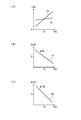
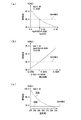
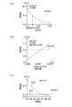
- FIG. (A) is a graph showing the Ids-Vgs characteristics in the saturation region at Vgs> Vth of a general NMOS transistor.
- (B) is a graph showing the Ids-Vds characteristics at Vgs> Vth of a general NMOS transistor.
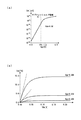
- (A) is a graph showing the Ids-Vgs characteristics in the linear region at Vgs> Vth of a general NMOS transistor.
- (B) is a graph showing the relationship between the resistance value and Vgs in the linear region when Vgs> Vth of a general NMOS transistor. It is a graph which shows the temperature dependence of the drain current in the linear region with Vgs> Vth of a general NMOS transistor.
- (A) is a graph showing the Ids-Vgs characteristics in the saturation region at Vgs> Vth of a general NMOS transistor.
- (B) is a graph showing the temperature dependence of the drain current in the saturation region at Vgs> Vth of a general NMOS transistor.
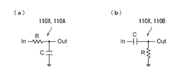
- (A) is a circuit diagram showing a first example of a voltage controlled voltage source according to the first embodiment.
- FIG. (B) is a circuit diagram showing a second example of the voltage controlled voltage source according to the first embodiment. It is a circuit diagram which shows an example of the temperature detection part and the correction voltage generation part which concerns on Embodiment 1.
- FIG. (A) is a graph showing the temperature dependence of the first current and the second current according to the first embodiment.
- (B) is a graph showing the temperature dependence of the differential current according to the first embodiment.
- (C) is a graph showing the temperature dependence of the correction voltage according to the first embodiment.
- (A) is a graph showing the temperature dependence of the first current and the second current when the current value of the first current according to the first embodiment is changed.
- (B) is a graph showing the temperature dependence of the first current and the second current when the current value of the second current according to the first embodiment is changed.
- (C) is a graph showing the temperature dependence of the differential current when the current value of the differential current according to the first embodiment is changed.
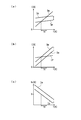
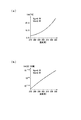
- (A) is a graph showing the relationship between the correction coefficient and the resistance value of the transistor at a plurality of different temperatures according to the first embodiment.
- (B) is a graph showing the effect of temperature correction on the temperature dependence of the resistance value of the transistor with respect to the first embodiment.
- (A) is a graph showing an R- ⁇ curve showing a resistance value of a transistor with respect to a correction coefficient at any two different temperatures according to the first embodiment.
- (B) is a graph showing the R- ⁇ curves showing the resistance values of the transistors with respect to the correction coefficients at the first temperature and the second temperature with respect to the first embodiment.
- (A) is a graph showing the relationship between the reference voltage at the first temperature and the resistance value of the transistor with respect to the first embodiment.
- (B) is a graph showing the relationship between the correction coefficient at the second temperature and the resistance value of the transistor with respect to the first embodiment.
- (C) is a graph showing the effect of temperature correction on the temperature dependence of the resistance value of the transistor with respect to the first embodiment.
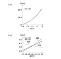
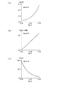
- (A) is a semi-logarithmic graph showing the Ids-Vgs characteristics of a general NMOS transistor.
- (B) is a graph showing the Ids-Vds characteristics in the subthreshold region of a general NMOS transistor.
- (A) is a graph showing the Ids-Vgs characteristics in the subthreshold region of a general NMOS transistor.
- (B) is a semi-logarithmic graph showing the Ids-Vgs characteristics in the subthreshold region of a general NMOS transistor.
- (C) is a graph showing the relationship between the resistance value and Vgs in the subthreshold region of a general NMOS transistor.
- (A) is a graph showing the temperature dependence of the drain current in the subthreshold region of a general NMOS transistor.
- FIG. 1A is a diagram for explaining a first example of a method for measuring a resistance value of a transistor according to the first embodiment.
- FIG. (B) is a diagram for explaining a second example of the method for measuring the resistance value of the transistor according to the first embodiment.
- (A) is a diagram showing an electronic circuit device including the resistance device according to the first embodiment.
- (B) is a graph generalizing the relationship between the physical quantity measurable from the electronic circuit according to the first embodiment and the correction coefficient.
- (A) is a circuit diagram of an integral filter as an RC filter circuit according to the first embodiment.
- (B) is a circuit diagram of a differential filter as an RC filter circuit according to the first embodiment. It is a circuit diagram of the active filter circuit which concerns on Embodiment 1.
- FIG. It is a flowchart which shows the correction coefficient determination method which concerns on Embodiment 1.
- (A) is a flowchart showing step S3 of FIG. 22.
- (B) is a flowchart showing step S4 of FIG. 22.
- (A) to (d) are diagrams showing resistance devices according to the first modified example to the fourth modified example of the first embodiment. It is a figure which shows the resistance device which concerns on Embodiment 2 of this invention. It is a graph which shows the temperature dependence of the correction voltage which concerns on Embodiment 2.
- (A) is a graph showing the temperature dependence of the first current and the second current according to the second embodiment.
- (B) is a graph showing the temperature dependence of the differential current according to the second embodiment.
- (C) is a graph showing the temperature dependence of the correction voltage according to the second embodiment.
- (A) is a graph showing the R- ⁇ curves showing the resistance values of the transistors with respect to the correction coefficients at the first temperature and the second temperature with respect to the second embodiment, respectively.
- (B) is a graph showing the relationship between the reference voltage at the first temperature and the resistance value of the transistor according to the second embodiment.
- (C) is a graph showing the relationship between the correction coefficient at the second temperature and the resistance value of the transistor with respect to the second embodiment.
- (A) is a circuit diagram showing an example of the voltage application circuit according to the second embodiment.
- (B) is a diagram showing the temperature dependence of the PTAT current according to the second embodiment. It is a circuit diagram which shows an example of the PTAT circuit which concerns on Embodiment 2.
- FIG. 5 is a graph showing that the first temperature at which the PTAT current according to the second embodiment becomes zero can be changed.
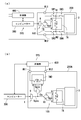
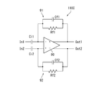
- (A) to (d) are diagrams showing resistance devices according to the first modification to the fourth modification of the second embodiment. It is a figure which shows the resistance device which concerns on Embodiment 3 of this invention. It is a figure which shows the brain machine interface apparatus which concerns on Embodiment 4 of this invention. It is a circuit diagram which shows an example of the integrated circuit apparatus which concerns on Embodiment 4.
- the reference code attached to the current may be used as a code representing the "current value” of the current
- the reference code attached to the voltage may be used as the code representing the "voltage value” of the voltage
- the reference code attached to the resistance element may be used as a code indicating the resistance or the "resistance value” of the resistance element.
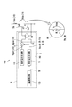
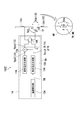
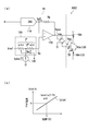
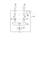
- FIG. 1 is a diagram showing a resistor device 100 according to the first embodiment.
- the resistance device 100 includes a field effect transistor TN and a voltage application circuit 1.
- the field effect transistor TN is an N-type field effect transistor.
- the field effect transistor TN is an n-type MOSFET (n-type Meter-Oxide-Semiconductor Field-Effective Transistor), that is, an NMOS transistor.
- transistor TN the field effect transistor TN may be referred to as "transistor TN".
- the back gate terminal of the field effect transistor TN may be connected to the source terminal or drain terminal of the field effect transistor TN, or may be connected to the ground or ground.
- the field effect transistor TN functions as a resistance element. Specifically, the field-effect transistor TN functions as a resistance element by utilizing the resistance between the drain and the source of the field-effect transistor TN. That is, the field effect transistor TN functions as a MOS resistor.
- MOS resistor For example, “CAMead,” Analog VLSI and Neural Systems “, Addison-Wesley Publishing Company, 1989.” or “T. Delbruck and CA Mead,” Adaptive photoreceptor with Wide dynamic range ", Proceedings of IEEE International Symposium on Circuits and Systems, 1994.”
- the field-effect transistor TN is a resistance element by utilizing the resistance between the drain and the source in the region (linear region and saturation region) where the gate-source voltage of the field-effect transistor TN is larger than the threshold voltage. Functions as. Further, the field effect transistor TN functions as a resistance element by utilizing the resistance between the drain and the source in the region (subthreshold region) where the voltage between the gate and the source of the field effect transistor TN is smaller than the threshold voltage.
- the MOS resistance MR has a resistance value R corresponding to the resistance value between the drain and the source of the field effect transistor TN.
- a voltage Vds corresponding to the voltage between the drain and the source of the field effect transistor TN is applied to the MOS resistance MR
- the current Ids corresponding to the drain current flowing between the drain and the source of the field effect transistor TN is applied to the MOS resistance MR.
- the resistance value R between the drain and the source of the field effect transistor TN may be described as "the resistance value R of the field effect transistor TN".
- the voltage application circuit 1 applies a control voltage Vgs corresponding to the temperature T between the gate and the source of the field effect transistor TN to control the resistance value R between the drain and the source of the field effect transistor TN.
- "Between the gate and the source of the field effect transistor TN” means "between the gate terminal and the source terminal of the field effect transistor TN”.
- the temperature T indicates the ambient temperature of the resistance device 100.
- the control voltage Vgs has a positive value.
- the control voltage Vgs indicates the voltage between the gate and the source of the field effect transistor TN.
- control voltage Vgs may be described as “gate-source voltage Vgs”. Further, the voltage Vds between the drain and the source may be described as “drain-source voltage Vds”.
- the control voltage Vgs indicates the voltage obtained by adding the correction voltage Vc to the reference voltage Vgs0. Specifically, the control voltage Vgs is represented by the equation (1).
- Vgs Vgs0 + Vc ... (1)
- the correction voltage Vc is a voltage added to the reference voltage Vgs0 in order to reduce the temperature dependence of a desired physical quantity on the field effect transistor TN.
- the physical quantity relating to the field effect transistor TN is a physical quantity including the resistance value R of the field effect transistor TN, which can be measured from an electronic circuit including the field effect transistor TN.
- the physical quantity of the field-effect transistor TN is, for example, the resistance value R between the drain and the source of the field-effect transistor TN, or the cutoff frequency fc of the filter circuit including the field-effect transistor TN.
- "Physical quantity including resistance value R" indicates a physical quantity depending on resistance value R.
- a desired physical quantity relating to the field effect transistor TN may be described as a “target physical quantity”. Therefore, the target physical quantity is a physical quantity including the resistance value R of the field effect transistor TN, which can be measured from an electronic circuit including the field effect transistor TN, and indicates a physical quantity set as a target value.
- the correction voltage Vc is represented by the equation (2).
- ⁇ indicates a correction coefficient
- T indicates a temperature
- T1 indicates a first temperature.
- the correction coefficient ⁇ is a coefficient for determining the correction voltage Vc.
- the correction coefficient ⁇ has a negative value. Therefore, the correction voltage Vc becomes smaller as the temperature T becomes higher.
- the correction coefficient ⁇ is a coefficient for correcting the control voltage Vgs applied between the gate and the source of the field effect transistor TN in order to reduce the temperature dependence of a desired physical quantity with respect to the field effect transistor TN. is there.
- Vc ⁇ (T-T1) ... (2)
- the correction voltage Vc depends on the temperature T and is set to be zero at the first temperature T1.
- the first temperature T1 is the temperature at which the correction voltage Vc becomes zero. Therefore, according to the first embodiment, the effect of the correction is lost at the first temperature T1.
- the correction coefficient ⁇ when correcting the control voltage Vgs applied between the gate and source of the field effect transistor TN and the field effect transistor The combination with the desired physical quantity for TN can be efficiently determined. Details of this point will be described later.
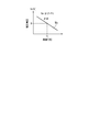
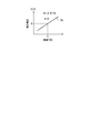
- FIG. 2 is a graph showing the correction voltage Vc.
- the vertical axis represents the correction voltage Vc [V]
- the horizontal axis represents the temperature T [K].
- the correction voltage Vc changes linearly with respect to the temperature T.
- the slope of the straight line indicating the correction voltage Vc indicates the correction coefficient ⁇ .
- a correction voltage Vc that changes linearly according to the temperature T shown in the equation (2) is added to the reference voltage Vgs0 as in the control voltage Vgs shown in the equation (1).
- the reason why the temperature dependence of the field effect transistor TN as the MOS resistance MR can be corrected will be described.
- the “Vgs> Vth” region is the operating region of the NOMS transistor when the magnitude of the gate-source voltage Vgs (voltage between the gate and source) is larger than the magnitude of the threshold voltage Vth.
- the “Vgs> Vth” region corresponds to an example of the “first operating region of the field effect transistor”.
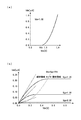
- FIG. 3A is a graph showing the Ids-Vgs characteristics in the saturation region of the "Vgs> Vth" region of a general NMOS transistor.
- the horizontal axis represents the gate-source voltage Vgs [V]
- the vertical axis represents the drain current Ids [ ⁇ A].
- FIG. 3B is a graph showing the Ids-Vds characteristics of a general NMOS transistor.
- the horizontal axis represents the drain-source voltage Vds [V], and the vertical axis represents the drain current Ids [ ⁇ A].
- the region represented by "Vds> Vgs-Vth" in the “Vgs> Vth” region is the saturation region of the NMOS transistor.
- the drain current Ids in the saturation region is represented by Eq. (3).
- Cox indicates the gate capacitance of the NMOS transistor
- ⁇ n indicates the electron mobility of the NMOS transistor.
- L indicates the gate length of the NMOS transistor, and W indicates the gate width of the NMOS transistor.
- the simulation results using the standard circuit parameters according to the equation (3) are shown in the "saturation region" of FIGS. 3 (a) and 3 (b).
- the drain current Ids flows.
- the drain current Ids is saturated to a substantially constant value in the saturation region. That is, in the saturation region, the drain current Ids does not depend on the drain-source voltage Vds.
- the region basically used in an NMOS transistor is the saturation region.
- the region represented by "Vds ⁇ Vgs-Vth" in the “Vgs> Vth” region is the linear region of the NMOS transistor.
- the drain current Ids in the linear region is represented by Eq. (4).
- the "linear region” in FIG. 3 (b) shows the simulation results using the standard circuit parameters according to the equation (4). As shown in FIG. 3B, in the “linear region”, the drain current Ids changes linearly with respect to the drain-source voltage Vds.
- the Ids-Vds characteristics can be linearly approximated, so that an NMOS transistor can be easily used as a MOS resistor as a preferable example.
- the drain current Ids can be controlled by the gate-source voltage Vgs.
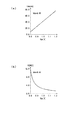
- FIGS. 4 (a) and 4 (b) show simulation results using standard circuit parameters based on equation (4).
- the drain current Ids increases linearly as the gate-source voltage Vgs increases in the range of several hundred mV. That is, the drain current Ids is proportional to the gate-source voltage Vgs in the range of several hundred mV.
- the resistance value R of the NMOS transistor as the MOS resistance can be expressed as in the equation (6), the resistance value R is inversely proportional to the gate-source voltage Vgs as shown in FIG. 4 (b).
- the MOS resistance by the NMOS transistor can be used as a linear resistance in the linear region in the “Vgs> Vth” region, for example, MOS.
- the current flowing through the resistor is proportional to the gate-source voltage Vgs
- the cutoff frequency fc of the RC filter composed of the MOS resistor is proportional to the gate-source voltage Vgs. That is, the current flowing through the MOS resistor and the cutoff frequency fc of the RC filter can be linearly controlled by Vgs.
- the threshold voltage Vth and electron mobility ⁇ n of the NMOS transistor are temperature dependent.
- the threshold voltage Vth considering the temperature dependence is expressed by the equation (7).
- ⁇ th indicates the temperature coefficient of the threshold voltage Vth.
- Vth_T0 indicates the threshold voltage Vth at the temperature T0. That is, as in the equation (7), the threshold voltage Vth changes from Vth_T0 according to the change from T0 of the temperature with the threshold voltage Vth_T0 obtained as an observed value at an arbitrary temperature T0 as a boundary.
- the electron mobility ⁇ n considering the temperature dependence is expressed by the equation (8).
- ⁇ indicates the temperature coefficient of electron mobility ⁇ n.
- ⁇ n_T0 indicates the electron mobility ⁇ n at the temperature T0. That is, as shown in the equation (8), the electron mobility obtained as an observed value at an arbitrary temperature T0 changes from ⁇ n_T0 in accordance with the change in temperature from T0 with ⁇ n_T0 as a boundary.
- the drain current Ids reflecting the temperature dependence of both the threshold voltage Vth and the electron mobility ⁇ n in the linear region of the NMOS transistor is determined. It is represented by the equation (9).
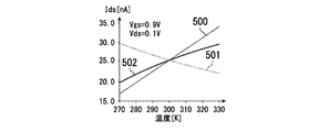
- FIG. 5 is a graph showing the temperature dependence of the drain current Ids in the linear region of the “Vgs> Vth” region of a general NMOS transistor.
- the horizontal axis represents the temperature [K], and the vertical axis represents the drain current Ids [nA].
- Line 502 shows the drain current Ids according to the equation (9) when the temperature dependence of both the electron mobility ⁇ n and the threshold voltage Vth is reflected.
- the drain current is considered only when the temperature dependence of the threshold voltage Vth is considered. Ids increases linearly with increasing temperature. Qualitatively, this is because the threshold voltage Vth decreases as the number of movable charged particles increases with increasing temperature.
- the temperature coefficient ⁇ of the electron mobility ⁇ n in the equations (8) and (9) takes a negative value, only the temperature dependence of the electron mobility ⁇ n is considered as shown by line 501 in FIG. Then, the drain current Ids decreases substantially linearly as the temperature rises. Qualitatively, when the temperature rises, the movement of charged particles is hindered by the thermal vibration of the silicon crystal lattice.
- the drain current Ids reflecting the temperature dependence of the threshold voltage Vth and the drain current Ids reflecting the temperature dependence of the electron mobility ⁇ n can be linearly approximated.
- the drain current Ids that reflect both the temperature dependence of the threshold voltage Vth and the temperature dependence of the electron mobility ⁇ n can also be linearly approximated.
- the drain current Ids increases substantially linearly with increasing temperature.
- the temperature dependence of the threshold voltage Vth has a greater effect on the drain current Ids than the temperature dependence of the electron mobility ⁇ n.
- the influence of the temperature dependence of the threshold voltage Vth is suppressed by the influence of the temperature dependence of the electron mobility ⁇ n.
- the threshold voltage Vth decreases by 85 mV by a temperature rise of 50 degrees. Further, the decrease width (85 mV) of the threshold voltage Vth is narrowed (less than 85 mV) due to the suppression effect due to the temperature dependence of the electron mobility ⁇ n.
- the amount of increase in the drain current Ids when the gate-source voltage Vgs is increased by 100 mV can be linearly approximated.
- the drain current Ids can be reduced by linearly lowering the gate-source voltage Vgs in response to the drain current Ids (line 502 in FIG. 5) that linearly increases as the temperature rises. Temperature dependence can be suppressed. As a result, the temperature dependence of the NMOS transistor as the MOS resistance can be corrected in the linear region of the "Vgs> Vth" region.
- the temperature shown in the equation (2) is set to the reference voltage Vgs0 like the control voltage Vgs shown in the equation (1) applied between the gate and the source of the transistor TN. It can be seen that the temperature dependence of the transistor TN as the MOS resistor MR can be corrected by adding the correction voltage Vc that changes linearly according to T.
- the reference voltage Vgs0 changes linearly according to the temperature T shown in the equation (2), as in the control voltage Vgs shown in the equation (1).
- the correction voltage Vc By adding the correction voltage Vc, the temperature dependence of the transistor TN as a MOS resistor can be corrected. This point will be described with reference to FIGS. 6 (a) and 6 (b).
- FIG. 6 (a) is a graph showing the drain current Ids with respect to the gate-source voltage Vgs in the saturation region in the “Vgs> Vth” region of a general NMOS transistor according to the equation (3).
- the drain current Ids can be linearly approximated in a range of about 100 mV, although there is non-linearity as compared with the linear region of FIG. 4A.
- the drain current Ids in the saturation region of the NMOS transistor reflecting the temperature dependence is represented by the equation (10) based on the equations (3), (7), and (8).
- FIG. 6B is a graph showing the temperature dependence of the drain current Ids in the saturation region of the “Vgs> Vth” region of a general NMOS transistor.
- the horizontal axis represents the temperature [K], and the vertical axis represents the drain current Ids [nA].
- Line 505 shows the drain current Ids according to the equation (10) when the temperature dependence of both the electron mobility ⁇ n and the threshold voltage Vth is reflected.
- the drain reflects both the temperature dependence of the threshold voltage Vth and the temperature dependence of the electron mobility ⁇ n.
- the current Ids can also be linearly approximated.
- the temperature coefficient ⁇ th of the standard threshold voltage Vth is -1.7 mV / K, and due to the effect of suppressing the electron mobility ⁇ n depending on the temperature, the saturation region has the same effect as the linear region.
- the amount of decrease in the threshold voltage Vth with the temperature rise of 50 degrees is less than 85 mV.
- the amount of increase in the drain current Ids when the gate-source voltage Vgs is increased by 100 mV can be linearly approximated.
- the drain current Ids is linearly decreased by linearly lowering the gate-source voltage Vgs in accordance with the drain current Ids (line 505 in FIG. 6B) that increases linearly with the temperature rise.
- the temperature dependence of the current Ids can be suppressed.
- the temperature dependence of the NMOS transistor as the MOS resistance can be corrected in the saturation region in the “Vgs> Vth” region.
- the reference voltage Vgs0 is shown in the equation (2) like the control voltage Vgs shown in the equation (1) applied between the gate and the source of the transistor TN. It can be seen that the temperature dependence of the transistor TN as the MOS resistor MR can be corrected by adding the correction voltage Vc that changes linearly according to the temperature T.
- a correction voltage Vc that changes linearly according to the temperature T shown in the equation (2) is added to the reference voltage Vgs0 like the control voltage Vgs shown in the equation (1) applied between the gate and the source of the transistor TN. Therefore, the temperature dependence of the transistor TN as the MOS resistance MR can be corrected.
- the voltage application circuit 1 is arranged between the gate terminal and the source terminal of the transistor TN.
- the potential of the source terminal (hereinafter, may be referred to as “source potential Vs”) can take any value.
- source potential Vs can take any value.
- the two terminals of the drain terminal and the source terminal of the transistor TN are used as the two terminals at both ends of the MOS resistor MR, they are electrically independent from the ground or ground (0 [V]) ( For example, it is used in a floating state.
- the source potential Vs can take any value.
- the voltage application circuit 1 includes a control voltage application unit 9 and a temperature detection unit 13.
- the temperature detection unit 13 detects the temperature T and outputs a detection signal TM corresponding to the temperature T to the control voltage application unit 9.
- the temperature detection unit 13 detects the temperature T and represents a detection signal TM representing a physical quantity (for example, current or voltage) indicating the temperature T, or a detection representing a physical quantity (for example, current or voltage) correlated with the temperature T.
- the configuration of the temperature detection unit 13 is not particularly limited.
- the temperature detection unit 13 may include a temperature sensor such as a thermistor.
- the temperature detection unit 13 may include a field effect transistor or a bipolar transistor and utilize the temperature-dependent characteristics of the field effect transistor or the bipolar transistor.
- the temperature detection unit 13 may include a PTAT (Proportional To Absolute Temperature) circuit.
- the PTAT circuit outputs a current proportional to the absolute temperature as a detection signal TM.
- the temperature detection unit 13 is configured by a temperature detection circuit that detects the temperature T and outputs the detection signal TM.
- the control voltage application unit 9 applies a control voltage Vgs corresponding to the detection signal TM indicating the temperature T between the gate and the source of the transistor TN. Specifically, the control voltage application unit 9 generates the control voltage Vgs so that the control voltage Vgs includes a correction voltage Vc that changes linearly with respect to the temperature T according to the detection signal TM. Then, the control voltage application unit 9 applies the control voltage Vgs between the gate and the source of the transistor TN. Therefore, according to the first embodiment, the temperature dependence of the resistance value R of the transistor TN can be appropriately reduced according to the detection signal TM indicating the temperature T.
- the control voltage application unit 9 includes a control voltage generation unit 10 and a voltage control voltage source 19. Further, the control voltage generation unit 10 includes a reference voltage generation unit 11, a correction voltage generation unit 15, and an addition unit 17.
- the reference voltage generation unit 11 generates the reference voltage Vgs0 in the equation (1) and outputs the reference voltage Vgs0 to the addition unit 17.
- the correction voltage generation unit 15 generates a correction voltage Vc that changes linearly with respect to the temperature T based on the temperature detection signal TM, and outputs the correction voltage Vc to the addition unit 17.
- the addition unit 17 adds the reference voltage Vgs0 and the correction voltage Vc to generate the control voltage Vgsa which is the addition result. In this way, the control voltage generation unit 10 generates the control voltage Vgsa.
- the control voltage Vgsa may be described as "reference control voltage Vgsa".
- the control voltage Vgsa is represented by the equation (11).
- Vgsa Vgs0 + Vc ... (11)
- the control voltage Vgsa and the control voltage Vgs have the same voltage component (reference voltage Vgs0 and correction voltage Vc) and the same voltage value.
- the correction voltage Vc is represented by the formula (2). As shown in FIG. 2, the correction voltage Vc represented by the formula (2) decreases linearly as the temperature T increases. That is, in the case of the transistor TN, the correction coefficient ⁇ takes a negative value. Then, by changing the correction coefficient ⁇ , the rate of lowering the control voltage Vgsa can be adjusted according to the temperature T.
- the control voltage Vgsa is specifically a voltage based on 0 [V] (that is, a potential difference based on 0 [V]).
- the source potential Vs of the transistor TN can take any value. Therefore, when the control voltage Vgsa is applied directly between the gate and the source, when the source potential Vs of the transistor TN takes an arbitrary value independently of the ground or ground (0 [V]), "Vgsa-Vs" becomes the transistor TN. It becomes the voltage between the gate and the source. As a result, the resistance value R of the transistor TN can change according to the source potential Vs. Therefore, in the first embodiment, the control voltage Vgsa is indirectly applied between the gate and the source of the transistor TN.
- the control voltage application unit 9 has a voltage control voltage source 19.
- the control voltage between the gate and the source of the transistor TN. Vgsa may be applied directly.
- the voltage control voltage source 19 is connected between the gate terminal and the source terminal of the transistor TN.
- the voltage control voltage source 19 has two terminals for input and two terminals for output.
- the voltage control voltage source 19 is a voltage source in which the potential difference between the two output terminals is determined according to the potential difference between the two input terminals.
- the control voltage Vgsa is input as a potential difference by inputting the control voltage Vgsa with reference to 0 [V] and the reference voltage 0 [V] to the voltage control voltage source 19 from the control voltage generation unit 10. Will be done.
- control voltage Vgsa may be input to the voltage control voltage source 19 as a potential difference
- the reference voltage 0 [V] may be set to an arbitrary value. In this case, if the reference voltage is Vref and the output voltage from the control voltage generation unit 10 is "Vgsa + Vref", the potential difference input to the voltage control voltage source 19 becomes Vgsa by "Vgsa + Vref-Vref". ..
- the voltage application circuit 1 of FIG. 1 can apply an arbitrary control voltage Vgs represented by the equation (1) between the gate and the source of the transistor TN.
- the drain current Ids of the MOS resistance MR composed of the transistor TN increases substantially linearly as the temperature T rises (line 502 in FIG. 5 and line 505 in FIG. 6 (b)).
- the correction coefficient ⁇ of the correction voltage Vc (FIG. 2) in the voltage application circuit 1 the voltage application circuit 1 linearly lowers the control voltage Vgs according to the temperature T to reduce the drain current Ids. Decrease linearly.
- the temperature dependence of the drain current Ids can be suppressed. If the temperature dependence of the drain current Ids can be suppressed, the temperature dependence of the physical quantity with respect to the transistor TN can be suppressed.
- FIG. 7A is a circuit diagram showing a first example of the voltage controlled voltage source 19.
- the voltage controlled voltage source 19 according to the first example includes a first switch circuit 191 and a second switch circuit 192, and a capacitor 193.
- the first switch circuit 191 includes terminals t1 to t3.
- the terminal t1 is connected to the control voltage generation unit 10.
- the terminal t2 is connected to the gate terminal of the transistor TN.
- the terminal t3 is connected to one terminal of the capacitor 193.
- the second switch circuit 192 includes terminals t4 to t6.
- the terminal t4 is connected to the control voltage generation unit 10.
- the terminal t5 is connected to the source terminal of the transistor TN.
- the terminal t6 is connected to the other terminal of the capacitor 193.
- the control voltage generation unit 10 generates the control voltage Vgsa.
- the first switch circuit 191 connects the terminal t3 and the terminal t1.
- the second switch circuit 192 connects the terminal t6 and the terminal t4.
- the capacitor 193 holds the control voltage Vgsa.
- the first switch circuit 191 connects the terminal t3 and the terminal t2.
- the second switch circuit 192 connects the terminal t6 and the terminal t5.
- the control voltage Vgsa held in the capacitor 193 is applied as the control voltage Vgs between the gate and the source of the transistor TN.
- FIG. 7B is a circuit diagram showing a second example of the voltage controlled voltage source 19.
- the voltage-controlled voltage source 19 according to the second example further includes an operational amplifier 194 in addition to the configuration of the voltage-controlled voltage source 19 according to the first example.
- the points that the second example differs from the first example will be mainly described.
- the output terminal of the operational amplifier 194 is connected to the node N.
- the node N is located on the line connecting the terminal t2 and the gate terminal of the transistor TN.
- the inverting input terminal of the operational amplifier 194 is connected to the terminal t5.
- the non-inverting input terminal of the operational amplifier 194 is connected to the source terminal of the transistor TN.
- the operation of the voltage controlled voltage source 19 according to the second example is the same as the operation of the voltage controlled voltage source 19 according to the first example.
- the source terminal of the transistor TN is connected to the non-inverting input terminal of the operational amplifier 194
- the influence of the capacitive load of the gate terminal and the source terminal of the transistor TN can be reduced as compared with the first example. ..
- the configuration of the voltage-controlled voltage source 19 is not particularly limited as long as the voltage-controlled voltage source 19 can be inserted between any two terminals that are electrically floating.
- control voltage generation unit 10 is not particularly limited as long as the control voltage Vgsa represented by the equation (11) can be generated, and can be configured by an arbitrary control voltage generation circuit.
- FIG. 1 shows the physical or logical configuration of the control voltage generation unit 10. Therefore, when FIG. 1 shows the physical configuration of the control voltage generation unit 10, for example, the reference voltage generation unit 11 is configured by the reference voltage generation circuit that generates the reference voltage Vgs0, and the correction voltage generation unit 15 is The correction voltage generation circuit that generates the correction voltage Vc based on the detection signal TM of the temperature detection unit 13 is configured, and the addition unit 17 is composed of an addition circuit that adds the correction voltage Vc to the reference voltage Vgs0.
- FIG. 1 shows the logical configuration of the control voltage generation unit 10, for example, when the reference voltage generation unit 11, the correction voltage generation unit 15, and the addition unit 17 are not clearly distinguished as a physical configuration.
- the control voltage generation unit 10 generates the control voltage Vgsa represented by the equation (11), the circuit constituting the control voltage generation unit 10 is not particularly limited.
- FIG. 1 shows the physical or logical configuration of the temperature detection unit 13 and the correction voltage generation unit 15. Therefore, when the temperature detection unit 13 and the correction voltage generation unit 15 represent a logical configuration, for example, the temperature detection unit 13 and the correction voltage generation unit 15 are not clearly distinguished as a physical configuration. Is not particularly limited as long as the correction voltage Vc represented by the equation (2) can be generated, and can be configured by any temperature detection circuit and correction voltage generation circuit.
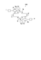
- FIG. 8 is a circuit diagram showing an example of the temperature detection unit 13 and the correction voltage generation unit 15.
- the temperature detection unit 13 and the correction voltage generation unit 15 include a first current source circuit 131, a second current source circuit 133, and a variable resistor Ro.
- the first current source circuit 131 and the second current source circuit 133 are connected in series between the first power supply line PL1 and the second power supply line PL2.
- One terminal of the variable resistor Ro is connected to the node Nc between the first current source circuit 131 and the second current source circuit 133.
- the other terminal of the variable resistor Ro is grounded.
- the potential of the first power supply line PL1 takes a positive value, and for example, the first power supply line PL1 is connected to a positive power supply that supplies a positive power supply voltage.
- the potential of the second power supply line PL2 takes a negative value, and for example, the second power supply line PL2 is connected to a negative power supply that supplies a negative power supply voltage.
- the first current source circuit 131 generates the first current Ip.
- the second current source circuit 133 generates a second current Im.
- a differential current Io flows through the variable resistor Ro.
- the differential current Io is a current indicating the difference between the first current Ip and the second current Im.
- a potential difference Vc is generated between both ends of the variable resistor Ro.
- the temperature detection unit 13 and the correction voltage generation unit 15 are not clearly distinguished, but the temperature dependence between the first current source circuit 131 and the second current source circuit 133 is used for temperature detection.
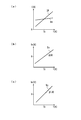
- a graph showing the temperature dependence of the first current Ip and the second current Im is shown in FIG. 9A.
- the horizontal axis is the temperature T [K]
- the vertical axis is the current value I [A] of each current source circuit.
- each of the first current Ip and the second current Im changes linearly with the change of the temperature T.
- the temperature dependence of the first current Ip and the temperature dependence of the second current Im are different. That is, the temperature dependence of the first current source circuit 131 of the temperature detection unit 13 and the temperature dependence of the second current source circuit 133 are different.
- the temperature dependence of the first current Ip is lower than the temperature dependence of the second current Im. That is, the temperature dependence of the first current source circuit 131 is lower than the temperature dependence of the second current source circuit 133.
- the horizontal axis is the temperature T [K]
- the vertical axis is the differential current value Io [A].
- the differential current Io has a negative temperature characteristic. That is, the slope A of the straight line representing the differential current Io has a negative value. Further, in FIG.
- the differential current Io is represented by the equation (12).
- the first current source circuit 131 and the second current source circuit 133 connected in series constitute the temperature detection unit 13 in FIG. 1.
- the differential current Io may be considered as the detection signal TM of the temperature detection unit 13 in FIG.
- the correction voltage Vc when the differential current Io is input to the variable resistor Ro is expressed by the equation (13).
- a graph showing the temperature dependence of the correction voltage Vc is shown in FIG. 9 (c).
- the horizontal axis is the temperature T [K]
- the vertical axis is the correction voltage Vc [V]. Since the differential current Io has a negative temperature characteristic, the correction voltage Vc also has a negative temperature characteristic as shown in FIG. 9C. That is, it matches the graph of the temperature dependence of the correction voltage Vc shown in FIG. Further, when the temperature is the first temperature T1, the correction voltage Vc becomes zero as shown in FIG. 9C.
- the correction coefficient ⁇ is “Ro ⁇ A” as shown in the equation (13), and takes a negative value like the slope A in the equation (12). Then, when it is desired to change the correction coefficient ⁇ , it can be seen that the variable resistor Ro should be changed.
- the variable resistor Ro may be considered as the correction voltage generation unit 15 in FIG. Further, as is clear from the equation (13), the correction voltage Vc has a value based on the differential current Io.
- the first temperature T1 at which the differential current Io and the correction voltage Vc become zero can be changed by the following method.
- a method of changing the first temperature T1 shown in the formulas (2), (12) and (13) will be described with reference to FIGS. 8 and 10 (a) to 10 (c).
- FIG. 10A shows a graph showing the temperature dependence of the first current Ip and the second current Im when the current value of the first current Ip is changed.
- the temperature at which the first current Ip and the second current Im are equal is the first temperature T1. Therefore, as the current value of the first current Ip increases, so does the first temperature T1. That is, the first temperature T1 can be changed by the first current source circuit 131 changing the current value of the first current Ip.
- the first temperature T1 can also be changed by changing the current value of the second current Im by the second current source circuit 133.
- FIG. 10B shows a graph showing the temperature dependence of the first current Ip and the second current Im when the current value of the second current Im is changed. However, as shown in FIG. 10B, when the current value of the second current Im increases, the first temperature T1 decreases.
- FIG. 10C shows a graph showing the temperature dependence of the differential current Io when the current value of the differential current Io is changed.
- the temperature T is such that the differential current Io becomes zero.
- the first temperature T1 also increases.
- the correction voltage Vc also becomes zero.
- the first current source circuit 131 and the second current source circuit 133 are provided, the first current Ip and / or the second current Im is changed, and the differential current Io is set.
- the first temperature T1 which is the temperature T when the correction voltage Vc becomes zero, can be easily changed.
- the second power supply line PL2 may be grounded.
- one terminal of the variable resistor Ro is connected to the node Nc, and the other terminal of the variable resistor Ro is connected to a reference voltage source that generates a reference voltage Vref (0 ⁇ Vref ⁇ PL1 potential).
- Vref reference voltage
- the slopes of the straight lines representing the first current Ip and the second current Im are both positive values, but they do not necessarily have to be positive values.
- the slope of the second current Im may be larger than the slope of the first current Ip. , The sign of the slope is irrelevant.
- the temperature dependence of the transistor TN can be corrected by appropriately setting the correction coefficient ⁇ of the correction voltage Vc according to the configuration of the resistance device 100 according to the first embodiment shown in FIG.
- the drain current Ids of the transistor TN in the linear region (Vds ⁇ Vgs-Vth) in the “Vgs> Vth” region Is expressed by the equation (14) reflecting the correction coefficient ⁇ .
- the drain current Ids of the transistor TN can be changed in the saturation region (Vds> Vgs-Vth) in the “Vgs> Vth” region. It is expressed by the equation (15) reflecting the correction coefficient ⁇ .
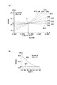
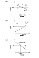
- FIG. 11A is a graph showing the relationship between the correction coefficient ⁇ and the resistance value R of the transistor TN at a plurality of different temperatures.
- the horizontal axis represents the correction coefficient ⁇
- the vertical axis represents the resistance value R [M ⁇ ].
- the reference voltage Vgs0 is 0.9V, and the drain-source voltage Vds is 1.8V.
- the gradients of the R- ⁇ curves G10 to G16 are different from each other depending on the temperature T.
- the R- ⁇ curves G10 to G16 intersect at almost one point P.
- the resistance value R of the transistor TN is substantially independent of the temperature T.
- the correction coefficient ⁇ (Rp) is set.
- the temperature dependence of the transistor TN can be offset by the correction voltage Vc including).
- the resistance value R of the transistor TN can be reduced.
- the resistance value R of the transistor TN can be maintained substantially constant with respect to fluctuations in the temperature T.
- the fact that the resistance value R is substantially independent of temperature may be described as “independent of temperature” or “independent of temperature”.
- the correction coefficient ⁇ (Rp) at least two R- ⁇ curves may be calculated. As can be understood from the equations (15) and (16), when the reference voltage Vgs0 changes, the R- ⁇ curve also changes. Therefore, when the reference voltage Vgs0 changes, the position of the intersection P changes. As a result, when the reference voltage Vgs0 changes, the correction coefficient ⁇ (Rp) also changes.
- the resistance value R of the transistor TN of the resistor device 100 shown in FIG. 1 is actually measured while changing the correction coefficient ⁇ , and an R- ⁇ curve of 2 or more is obtained. Then, the correction coefficient ⁇ (Rp) at the intersection P of two or more R- ⁇ curves is acquired. Further, the correction coefficient ⁇ (Rp) is set to the correction coefficient ⁇ of the correction voltage generation unit 15 of the resistance device 100. In particular, since the R- ⁇ curve is actually measured, the correction coefficient ⁇ (Rp) suitable for the transistor TN actually used can be determined. As a result, the temperature dependence of the resistance value R of the transistor TN can be further reduced.
- the temperature T indicates the ambient temperature of the resistance device 100, for example, the resistance device 100 is arranged in a constant temperature bath, and the temperature T is set by the constant temperature bath.
- the correction coefficient ⁇ (Rp) when the resistance value R does not depend on the temperature T is based on the intersection of the R- ⁇ curves G10 to G16. ) Can be obtained.
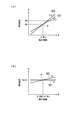
- FIG. 12A is a graph showing R- ⁇ curves G21 and G22 showing the resistance value R of the transistor TN with respect to the correction coefficient ⁇ at any two different temperatures T11 and T12, respectively.
- the horizontal axis represents the correction coefficient ⁇
- the vertical axis represents the resistance value R.
- the resistance value R of the transistor TN of the resistance device 100 is measured while changing the correction coefficient ⁇ , and the two R- ⁇ curves G21 and G22 are obtained. Then, the correction coefficient ⁇ (Rr) is acquired from the intersection P of the two R- ⁇ curves G21 and G22.
- the resistance value R when the correction coefficient ⁇ is the correction coefficient ⁇ (Rr) is a resistance value Rr having no temperature dependence. Therefore, when the correction coefficient ⁇ (Rr) is set to the correction coefficient ⁇ of the correction voltage generation unit 15 of the resistance device 100, the temperature dependence of the resistance value R of the transistor TN can be effectively reduced by the correction voltage Vc. As a result, the resistance value R of the transistor TN can be maintained at the resistance value Rr.
- the resistance value Rr having no temperature dependence at the intersection P and the desired resistance value Rd (hereinafter, may be referred to as "target resistance value Rd") basically do not match. This is because, as shown in FIG. 12A, the resistance value R of the transistor TN at arbitrary temperatures T11 and T12 fluctuates according to the correction coefficient ⁇ . Therefore, at the time of obtaining the R- ⁇ curve at each temperature, the intersection point P It is unknown what kind of resistance value Rr will be.
- the resistance value R with respect to the correction coefficient ⁇ is measured at two different temperatures while changing the reference voltage Vgs0, and R-with respect to the reference voltage Vgs0. It is required to repeatedly search for the intersection of the ⁇ curves until the resistance value Rr and the target resistance value Rd at the intersection match.
- the temperature T of 320K corresponds to the first temperature T1.
- FIG. 12B shows an R- ⁇ curve G31 showing the resistance value R of the transistor TN with respect to the correction coefficient ⁇ at the first temperature T1 and R showing the resistance value R of the transistor TN with respect to the correction coefficient ⁇ at the second temperature T2. It is a graph which showed the relationship with - ⁇ curve G32.
- the horizontal axis represents the correction coefficient ⁇
- the vertical axis represents the resistance value R.
- the second temperature T2 is different from the first temperature T1.
- the R- ⁇ curve G31 shows the resistance value R of the transistor TN at the first temperature T1.
- the first temperature T1 indicates the temperature when the physical quantity with respect to the transistor TN is substantially constant with respect to the change in the correction coefficient ⁇ .
- the first temperature T1 indicates the temperature when the resistance value R of the transistor TN is substantially constant with respect to the change of the correction coefficient ⁇ . That is, the first temperature T1 is the temperature at which the correction voltage Vc becomes zero.
- the resistance value R is a resistance value Rr having no temperature dependence.
- the resistance value R of the resistance device 100 is actually measured while changing the reference voltage Vgs0, and the resistance value R becomes the target resistance value Rd.
- the reference voltage Vgs0 (Rd) is obtained.
- the reference voltage Vgs0 is set to the reference voltage Vgs0 (Rd)
- the temperature T is set to the second temperature T2 different from the first temperature T1
- the resistance value R is changed while changing the correction coefficient ⁇ .
- the R- ⁇ curve G32 is obtained by actually measuring.
- the R- ⁇ curve G32 shows the resistance value R of the transistor TN at the second temperature T2.
- the correction coefficient ⁇ (Rr) at the intersection P of the R- ⁇ curve G31 at the first temperature T1 and the R- ⁇ curve G32 at the second temperature T2 is acquired.
- the temperature-independent resistance value Rr corresponding to the correction coefficient ⁇ (Rr) always matches the target resistance value Rd.
- the correction coefficient ⁇ (Rr) at the intersection P also coincides with the correction coefficient ⁇ (Rd) with respect to the target resistance value Rd. Therefore, according to the first embodiment, when the correction coefficient ⁇ (Rd) is set to the correction coefficient ⁇ of the correction voltage generation unit 15 of the resistance device 100, the temperature dependence of the resistance value R of the transistor TN is effective depending on the correction voltage Vc. The resistance value R of the transistor TN can be maintained at the target resistance value Rd.
- the second temperature T2 is set to a value near the temperature at which the transistor TN is actually used to obtain the correction coefficient ⁇ (Rd).
- the second temperature T2 is set to 310K, which is a value near the human body temperature
- the first temperature T1 is set to the first temperature. 2 Set to 320K, which is a value near the temperature T2.
- the intersection of the R- ⁇ curve G11 corresponding to the first temperature T1 of 320K and the R- ⁇ curve G12 corresponding to the second temperature T2 of 310K is corrected.
- the coefficient ⁇ (Rp) is ⁇ 0.00115.
- the correction coefficient ⁇ (Rp) was set to ⁇ 0.00115, and the resistance value R of the transistor TN was calculated from the equations (15) and (16).
- FIG. 11B is a graph showing the effect of temperature correction on the temperature dependence of the resistance value R of the transistor TN.
- the curve 506 shows the case where the temperature correction is not performed, and the curve 507 shows the case where the temperature correction is performed.
- the horizontal axis represents the temperature T [K], and the vertical axis represents the resistance value R [M ⁇ ].
- the correction coefficient ⁇ of the equation (15) was set to zero, the resistance value R was calculated from the equation (16), and the curve 506 was plotted.
- the temperature dependence of the resistance value R is strong when the correction is not performed.
- the correction coefficient ⁇ of the equation (15) is set to ⁇ 0.00115 of the correction coefficient ⁇ (Rp) obtained from FIG. 11 (a), and the equation (16) is used.
- the resistance value R was calculated and the curve 507 was plotted.
- the resistance value R is substantially constant and indicates a value Rp. That is, the temperature dependence of the resistance value R of the transistor TN can be strongly suppressed by the correction based on the correction coefficient ⁇ (Rp).
- the reference voltage Vgs0 described with reference to FIG. 12A is changed.
- the first temperature T1 that does not depend on the correction coefficient ⁇ described with reference to FIG. 12 (b).
- the combination can be determined at a higher speed when it is uniquely determined by the intersection P of the R- ⁇ curve in the above and the R- ⁇ curve at the second temperature T2 different from the first temperature T1.
- a voltage application circuit 1 having a correction voltage generation unit 15 that generates such a correction voltage Vc is suitable.
- the target resistance value Rd corresponds to an example of "target physical quantity related to field effect transistor". That is, the target resistance value Rd is a resistance value of the field effect transistor TN that can be measured from an electronic circuit including the field effect transistor TN, and indicates a resistance value set as the target value.
- the horizontal axis represents the reference voltage Vgs0 [V].
- the horizontal axis represents the correction coefficient ⁇ .
- the vertical axis represents the resistance value R [M ⁇ ].
- the correction coefficient ⁇ is determined by (Procedure 1) and (Procedure 2) shown below.
- the resistance device 100 is placed in a constant temperature bath, and the ambient temperature of the resistance device 100 is set to the first temperature T1 by the constant temperature bath.
- the resistance value R is measured while changing the voltage value of the reference voltage Vgs0.
- the reference voltage Vgs0 (Rd) when the resistance value R indicates the target resistance value Rd is determined.
- the resistance value R of the transistor TN becomes the target resistance value Rd (40 M ⁇ in the example of FIG. 13 (b)) at the second temperature T2 and the reference voltage Vgs0 (Rd).
- the correction coefficient ⁇ (Rd) at the time of becoming is determined.
- the resistance device 100 is placed in a constant temperature bath, and the ambient temperature of the resistance device 100 is set to the second temperature T2 by the constant temperature bath.
- the reference voltage Vgs0 is set to the reference voltage Vgs0 (Rd) determined in (Procedure 1).
- the resistance value R is measured while changing the value of the correction coefficient ⁇ .
- the correction coefficient ⁇ (Rd) when the resistance value R indicates the target resistance value Rd is determined.
- Executing means that in FIG. 12B, the correction coefficient ⁇ at the intersection P of the R- ⁇ curve G31 at the first temperature T1 and the R- ⁇ curve G32 at the second temperature T2 ( Corresponds to acquiring Rd).
- the reason is as follows. That is, as shown in FIG. 12B, at the second temperature T2, the resistance value R coincides with the target resistance value Rd only at the intersection P. Therefore, the correction coefficient ⁇ when the resistance value R indicates the target resistance value Rd at the second temperature T2 always matches the correction coefficient ⁇ (Rd) at the intersection P. Further, at the intersection P, the resistance value R indicates the resistance value Rr having no temperature dependence, so that the target resistance value Rd matches the resistance value Rr having no temperature dependence.
- (procedure 1) and (procedure 2) match the resistance value Rr having no temperature dependence.
- the correction coefficient ⁇ (Rd) at which the target resistance value Rd to be obtained is obtained is determined. Therefore, it is not required to repeatedly obtain the intersection of the R- ⁇ curves at any two different temperatures while changing the reference voltage Vgs0. As a result, the combination of the target resistance value Rd and the correction coefficient ⁇ (Rd) having no temperature dependence can be determined quickly and uniquely.
- the value of the correction coefficient ⁇ (Rd) is different from the first temperature T1 based on the reference voltage Vgs0 (Rd) when the target resistance value Rd of the transistor TN is obtained at the first temperature T1.
- the value when the target resistance value Rd is obtained at the second temperature T2 is shown.
- a voltage application circuit 1 having a correction voltage generation unit 15 that generates a correction voltage Vc so that the correction effect disappears at the first temperature T1 is preferable. is there.
- the resistance value R shown in FIGS. 13 (a) and 13 (b) shows the simulation results based on the equations (15) and (16).
- FIG. 13C is a graph showing the effect of temperature correction on the temperature dependence of the resistance value R of the transistor TN.
- the curve 508 shows the case where the temperature correction is not performed, and the curve 509 shows the case where the temperature correction is performed.
- the horizontal axis represents the temperature T [K], and the vertical axis represents the resistance value R [M ⁇ ].
- the correction coefficient ⁇ of the formula (15) is set to zero
- the reference voltage Vgs0 is set to 0.8368V, which is the Vgs0 (Rd) obtained in (Procedure 1)
- the formula (16) is used.
- the resistance value R was calculated and the curve 508 was plotted. As is clear from the curve 508, the temperature dependence of the resistance value R is strong when the correction is not performed.
- the correction coefficient ⁇ of the equation (15) is set to ⁇ 0.00130, which is ⁇ (Rd) obtained in (Procedure 2), and the resistance value R is calculated from the equation (16).
- the curve 509 was plotted.
- the resistance value R is substantially constant and indicates a value Rd. That is, the temperature dependence of the resistance value R of the transistor TN can be strongly suppressed by the correction based on the correction coefficient ⁇ (Rd).
- the temperature correction of the drain current Ids and the resistance value R (MOS resistance) can be appropriately performed even in the saturated region with strong non-linearity. did it. Therefore, in the linear region (Vds ⁇ Vgs-Vth) having high linearity in the “Vgs> Vth” region, the temperature correction of the drain current Ids and the resistance value R (MOS resistance) can be performed more accurately.
- the correction coefficient ⁇ (Rp) corresponding to the resistance value Rp having no temperature dependence or the temperature dependence can be obtained by the same procedure as the procedure described with reference to FIGS. 11 (a) to 13 (c).
- the correction coefficient ⁇ (Rd) corresponding to the target resistance value Rd that does not exist is determined.
- the voltage application circuit 1 shown in FIG. 1 applies the control voltage Vgs between the gate and the source of the transistor TN to control the resistance value R between the drain and the source in the “Vgs> Vth” region of the transistor TN.
- the subthreshold region indicates the operating region (Vgs ⁇ Vth) of the transistor TN when the magnitude of the gate-source voltage Vgs (voltage between the gate and source) is less than the magnitude of the threshold voltage Vth.
- Vgs ⁇ Vth the operating region of the transistor TN when the magnitude of the gate-source voltage Vgs (voltage between the gate and source) is less than the magnitude of the threshold voltage Vth.
- the subthreshold region for example, when the aspect ratio (W / L) of the transistor TN is 0.01, a resistance value R of several M ⁇ to several tens of T ⁇ can be realized.
- the subthreshold region corresponds to an example of the “second operating region of the field effect transistor”.
- the drain current Ids increases exponentially with respect to the gate-source voltage Vgs. Therefore, the operating characteristics of the transistor TN as a MOS resistor are different from the saturation region and the linear region in the “Vgs> Vth” region.
- FIG. 14 (a) is a semi-logarithmic graph showing the Ids-Vgs characteristics of a general NMOS transistor.
- the horizontal axis represents the gate-source voltage Vgs [V]
- the vertical axis represents the drain current Ids [ ⁇ A] on a logarithmic scale.
- the region represented by “Vgs ⁇ Vth” is the subthreshold region.
- the logarithm log 10 Ids of the drain current Ids is proportional to the gate-source voltage Vgs.
- FIG. 14B is a graph showing the Ids-Vds characteristics in the subthreshold region of a general NMOS transistor.
- the horizontal axis represents the drain-source voltage Vds [V], and the vertical axis represents the drain current Ids [fA].
- the drain current Ids in the subthreshold region is expressed by the equation (17).
- the Vt of the formula (17) is called a thermal voltage and is represented by the formula (18).
- k is the Boltzmann constant and q is the elementary charge.
- ⁇ in the formula (17) is represented by the formula (19).
- Cd of the formula (19) is the depletion layer capacity.
- FIG. 14A shows the simulation result by the equation (17).
- the drain current Ids of the transistor TN increases according to an exponential function with respect to the increase of the gate-source voltage Vgs. Therefore, as shown in FIG. 14A, in the subthreshold region, the logarithm of the drain current Ids is proportional to the gate-source voltage Vgs.
- Vt kT / q ... (18)
- the range in which the Ids-Vds characteristic can be linearly approximated is as narrow as Vds ⁇ several tens of mV. Therefore, as an example, an NMOS transistor is used as a non-linear MOS resistor having a high resistance value.
- the drain current Ids can be linearly approximated as shown in the equation (20).
- the drain current Ids of the transistor TN saturates to a constant value.
- the drain current Ids is saturated to a constant value in the range of Vds> 100 mV.
- the Ids-Vds characteristic in the range of Vds> 100 mV corresponds to the saturation region in the "Vgs> Vth" region.
- the equation (17) showing the drain current Ids of the transistor TN in the subthreshold region (Vgs ⁇ Vth) is the equation (4) showing the drain current Ids of the transistor TN in the linear region in the “Vgs> Vth” region.
- the equation (3) showing the drain current Ids of the transistor TN in the saturation region are expressed by one equation.
- the resistance value R of the transistor TN is represented by the equation (21).
- the drain current Ids can be controlled exponentially by the gate-source voltage Vgs.
- FIG. 15 shows the relationship between the gate-source voltage Vgs, the drain current Ids, and the resistance value R in the subthreshold region of a general NMOS transistor.
- FIG. 15 is a simulation result using standard circuit parameters based on the equation (17).
- the horizontal axis of FIGS. 15 (a) to 15 (c) indicates the gate-source voltage Vgs [V].
- the vertical axis of FIG. 15A shows the drain current Ids [fA].
- the vertical axis of FIG. 15B shows the drain current Ids [A] of the semi-logarithmic graph with the vertical axis of FIG. 15A on a logarithmic scale.
- FIG. 15 (c) shows a graph of the drain current Ids of FIG. 15 (a) converted into a resistance value R by the equation (21), and the vertical axis shows the resistance value R [T ⁇ ].
- Vds was set to 0.1V.
- the threshold voltage Vth and electron mobility ⁇ n of the NMOS transistor are temperature-dependent.
- the electron mobility ⁇ n considering the temperature dependence is expressed by the equation (8).
- the drain current Ids reflecting the temperature dependence of both the electron mobility ⁇ n and the threshold voltage Vth in the subthreshold region is expressed by the equation (22). ..
- FIG. 16A is a graph showing the temperature dependence of the drain current Ids in the subthreshold region of the NMOS transistor according to the equation (22).
- the horizontal axis represents the temperature [K]
- the vertical axis represents the drain current Ids [fA].
- FIG. 16B is a semi-logarithmic graph in which the vertical axis of FIG. 16A is a logarithmic scale, the horizontal axis indicates the temperature [K], and the vertical axis is the drain current Ids [A] on the logarithmic scale. Is shown. 16 (a) and 16 (b) show simulation results using standard circuit parameters.
- the drain current Ids which reflects the temperature dependence of both the electron mobility ⁇ n and the threshold voltage Vth, increases exponentially as the temperature T rises. Therefore, as shown in FIG. 16B, the logarithm log 10 Ids of the drain current Ids is substantially proportional to the temperature T.
- the drain current Ids increases exponentially as the gate-source voltage Vgs increases. Therefore, as shown in FIG. 15B, the logarithm log 10 Ids of the drain current Ids is proportional to the gate-source voltage Vgs.
- the gate-source voltage Vgs is linearly lowered according to the drain current Ids that increases exponentially as the temperature rises, and the drain current Ids is exponentially reduced to determine the temperature dependence of the drain current Ids. Can be suppressed. As a result, the temperature dependence of the NMOS transistor as a MOS resistor can be corrected in the subthreshold region.
- the control voltage Vgs applied between the gate and the source of the transistor TN can be corrected by the linear function (correction voltage Vc) shown in the equation (2).
- the correction coefficient ⁇ (Rp) corresponding to the resistance value Rp having no temperature dependence or the temperature dependence can be obtained by the same procedure as the procedure described with reference to FIGS. 11 (a) to 13 (c).
- the correction coefficient ⁇ (Rd) corresponding to the target resistance value Rd that does not exist is determined.
- T 310K.
- the drain current Ids of the transistor TN is expressed by the equation (23) in the subthreshold region.
- the horizontal axis represents the voltage value [V].
- the horizontal axis represents the correction coefficient ⁇ .
- the vertical axis represents the resistance value R [T ⁇ ].
- the correction coefficient ⁇ is determined by (Procedure 1) and (Procedure 2) shown below.
- the reference voltage Vgs0 of the resistance device 100 is set to the reference voltage Vgs0 (Rd) determined in (Procedure 1).
- the resistance value R is measured while changing the value of the correction coefficient ⁇ , and the resistance value R indicates the target resistance value Rd (10 T ⁇ in the example of FIG. 17B).
- the correction coefficient ⁇ (Rd) is determined.
- the resistance value R shown in FIGS. 17 (a) and 17 (b) shows the simulation results based on the equations (21) and (23).
- FIG. 17C is a graph showing the effect of temperature correction on the temperature dependence of the resistance value R of the transistor TN.
- the curve 510 shows the case where the temperature correction is not performed, and the curve 511 shows the case where the temperature correction is performed.
- the horizontal axis represents the temperature T [K], and the vertical axis represents the resistance value R [T ⁇ ].
- the correction coefficient ⁇ of the formula (23) is set to zero
- the reference voltage Vgs0 is set to 0.2746V, which is the Vgs0 (Rd) obtained in (Procedure 1)
- the formula (21) is used.
- the resistance value R was calculated and the curve 510 was plotted. As is clear from the curve 510, the temperature dependence of the resistance value R is strong when the correction is not performed.
- the correction coefficient ⁇ of the equation (23) is set to ⁇ 0.00138, which is ⁇ (Rd) obtained in (Procedure 2), and the resistance value R is calculated from the equation (23).
- the resistance value R is substantially constant and indicates a value Rd. That is, the temperature dependence of the resistance value R of the transistor TN can be strongly suppressed by the correction based on the correction coefficient ⁇ (Rd).
- temperature correction can be performed in the entire range from the region where the drain current Ids of the transistor TN can be linearly approximated (linear region) to the region where the drain current Ids is saturated to a constant value (saturation region).
- the resistance value R of the transistor TN when determining the reference voltage Vgs0 and the correction coefficient ⁇ (for example, FIGS. 11A and 12B). ), FIG. 13 (a), FIG. 13 (b), FIG. 17 (a), and FIG. 17 (b)).
- the temperature detection unit 13 is omitted for the sake of simplification of the drawings.
- FIG. 18A is a diagram for explaining a first example of a method for measuring the resistance value R of the transistor TN according to the first embodiment.
- the resistance device 100 is mounted on the electronic circuit device 200.
- the electronic circuit device 200 is, for example, an integrated circuit device.
- the electronic circuit device 200 includes a resistance device 100, switches SW1 to SW4, an electronic circuit 3, a monitor terminal Mt1, and a monitor terminal Mt2.
- the transistor TN of the resistance device 100 is connected to the electronic circuit 3 via the switches SW3 and SW4.
- the switch SW1 and the switch SW3 are connected in series between the monitor terminal Mt1 and the electronic circuit 3.
- One end (drain terminal) of the transistor TN of the resistance device 100 is connected to the node N1 between the switch SW1 and the switch SW3.
- the switch SW2 and the switch SW4 are connected in series between the monitor terminal Mt2 and the electronic circuit 3.
- the other end (source terminal) of the transistor TN of the resistance device 100 is connected to the node N2 between the switch SW2 and the switch SW4.
- the switches SW1 and SW2 When measuring the resistance value R of the transistor TN and determining the reference voltage Vgs0 and the correction coefficient ⁇ , the switches SW1 and SW2 connect the transistor TN to the monitor terminals Mt1 and Mt2. Further, the switches SW3 and SW4 disconnect the transistor TN from the electronic circuit 3.
- the determined reference voltage Vgs0 and the correction coefficient ⁇ are set in the control voltage application unit 9, and the switches SW1 and SW2 are connected to the transistor TN and the electronic circuit 3 from the monitor terminals Mt1 and Mt2. To disconnect. Further, the switches SW3 and SW4 connect the transistor TN to the electronic circuit 3.
- the measurement system SYS measures the resistance value R of the transistor TN and processes the measurement data.
- the measuring system SYS includes a computer 300 and a measuring instrument 400.
- the measuring instrument 400 is connected to the monitor terminals Mt1 and Mt2. Then, the measuring instrument 400 measures the resistance value R of the transistor TN by applying a voltage Vds to both ends of the resistor formed by the transistor TN via the monitor terminals Mt1 and Mt2 and measuring the current Ids flowing through the resistor.
- the computer 300 sets the voltage value of the reference voltage Vgs0 in the reference voltage generation unit 11 of the control voltage application unit 9. Further, when the computer 300 searches for the reference voltage Vgs0 (Rd) with respect to the target resistance value Rd, the computer 300 changes the voltage value of the reference voltage Vgs0 set in the reference voltage generation unit 11.
- the computer 300 sets the value of the correction coefficient ⁇ for the correction voltage generation unit 15 of the control voltage application unit 9. Further, when the computer 300 searches for the correction coefficient ⁇ (Rd) with respect to the target resistance value Rd, the computer 300 changes the value of the correction coefficient ⁇ set in the correction voltage generation unit 15.
- the computer 300 controls the measuring instrument 400. Then, the computer 300 acquires measurement data indicating the resistance value R of the transistor TN from the measuring instrument 400. Further, the computer 300 processes the measurement data to determine the reference voltage Vgs0 (Rd) and the correction coefficient ⁇ (Rd) with respect to the target resistance value Rd.
- the transistor TN is connected to the monitor terminals Mt1 and Mt2, and the resistance value R of the transistor TN is directly measured. Therefore, the resistance value R can be measured with high accuracy.
- connecting the monitor terminals Mt1 and Mt2 to the transistor TN and connecting the switches SW3 and SW4 between the transistor TN and the electronic circuit 3 are the characteristics of the transistor TN and the characteristics of the transistor TN. It is effective when it does not affect the operation of the electronic circuit 3.
- FIG. 18B is a diagram for explaining a second example of the method for measuring the resistance value R of the transistor TN according to the first embodiment.
- the points that the second example differs from the first example will be mainly described.
- the resistance device 100 is mounted on the electronic circuit device 200A.
- the electronic circuit device 200A is, for example, an integrated circuit device.
- the electronic circuit device 200A includes a resistance device 100, an electronic circuit 3, a monitor terminal Mt1, a monitor terminal Mt2, a voltage controlled voltage source 19x, and a transistor TND.
- the configuration of the transistor TND is the same as the configuration of the transistor TN.
- the transistor TND is arranged in close proximity to the transistor TN.
- the resistance value of the transistor TND having the same configuration as the transistor TN (hereinafter referred to as “resistance value Rx”) is measured, and the resistance value Rx is estimated to be the resistance value R of the transistor TN. ..
- One terminal (drain terminal) of the transistor TND is connected to the monitor terminal Mt1, and the other terminal (source terminal) is connected to the monitor terminal Mt2.
- the transistor TN is connected to the electronic circuit 3.
- the configuration of the voltage controlled voltage source 19x is the same as the configuration of the voltage controlled voltage source 19.
- the voltage control voltage source 19x is connected to the control voltage application unit 9. Therefore, the voltage control voltage source 19x is a control voltage having the same voltage value as the control voltage Vgs generated by the voltage control voltage source 19 based on the control voltage Vgsa (hereinafter, referred to as “measurement control voltage Vgsx”). Is generated, and the measurement control voltage Vgsx is applied between the gate and the source of the transistor TND.
- the measuring instrument 400 measures the resistance value Rx of the transistor TND by applying a voltage Vds to both ends of the resistor formed by the transistor TND via the monitor terminals Mt1 and Mt2 and measuring the drain current flowing through the resistor. Then, the computer 300 acquires measurement data indicating the resistance value Rx of the transistor TND from the measuring instrument 400. Further, the computer 300 processes the measurement data to determine the reference voltage Vgs0 (Rd) and the correction coefficient ⁇ (Rd) with respect to the target resistance value Rd. That is, the computer 300 estimates that the resistance value Rx of the transistor TND is the resistance value R of the transistor TN, and determines the reference voltage Vgs0 (Rd) and the correction coefficient ⁇ (Rd).
- the resistance value Rx of the transistor TND having the same configuration as the transistor TN connected to the electronic circuit 3 is measured to measure the transistor.
- the resistance value R of TN is indirectly measured. Therefore, it is possible to prevent the monitor terminals Mt1 and Mt2 from affecting the characteristics of the transistor TN and the operation of the electronic circuit 3.
- the transistor TND it is preferable to arrange the transistor TND as close to the transistor TN as possible. This is because the variation in characteristics between the transistor TND and the transistor TN can be suppressed, and the degree of coincidence between the resistance value Rx and the resistance value R is further improved.
- the configuration of the electronic circuit 3 is not particularly limited as long as the transistor TN is connected to the electronic circuit 3.
- the electronic circuit 3 may include, for example, at least one of a transistor, a diode, a capacitor, an inductor, and a resistor.
- the temperature of the resistance value R of the transistor TN of the resistance device 100 can be corrected by a physical quantity other than the resistance value R.
- a physical quantity that can be measured from an electronic circuit including the resistance device 100 that performs temperature correction hereinafter referred to as "physical quantity G”
- the reference voltage Vgs0 and the correction coefficient ⁇ for temperature correction can be set. It is possible to decide.
- the physical quantity G that can be measured from the electronic circuit may be described as "physical quantity G of the electronic circuit”.
- FIG. 19A is a diagram showing an electronic circuit device 200B including the resistance device 100.
- the temperature detection unit 13 is omitted for the sake of simplification of the drawings.
- the electronic circuit device 200B includes the electronic circuit 3B and the resistance device 100.
- the transistor TN (MOS resistance MR) of the resistance device 100 is built in the electronic circuit 3B as a circuit element of the electronic circuit 3B.
- the input terminal In and the output terminal Out of the electronic circuit 3B are connected to the terminals Mt1 and Mt2 of the electronic circuit device 200B, respectively.
- the input terminal In and the output terminal Out of the electronic circuit 3B, and the terminals Mt1 and Mt2 of the electronic circuit device 200B are shown one by one, but the number of terminals is limited. There is no particular case, and the measuring instrument 400 and the electronic circuit 3B may be connected with the number of terminals required for measuring the physical quantity G of the electronic circuit 3B.
- the measurement system SYS includes a computer 300 and a measuring instrument 400.
- the measuring instrument 400 is connected to the input terminal In and the output terminal Out of the electronic circuit 3B via the terminals Mt1 and Mt2, and measures the physical quantity G of the electronic circuit 3B.
- the computer 300 controls the measuring instrument 400 and acquires measurement data from the measuring instrument 400.
- the physical quantity G that can be measured by the measuring instrument 400 from the electronic circuit 3B including the transistor TN (MOS resistance MR) of the resistance device 100 can be generalized and expressed as a function of the resistance value R of the transistor TN as shown in equation (24). .. Specifically, the resistance value R can be generalized and expressed as a function of the temperature T, the reference voltage Vgs0, and the correction coefficient ⁇ . Therefore, the physical quantity G expressed as a function of the resistance value R can also be generalized and expressed as a function of the temperature T, the reference voltage Vgs0, and the correction coefficient ⁇ .
- the temperature dependence of the physical quantity G which is a function of the resistance value R of the transistor TN, represented by the equation (24) is also corrected.
- the resistance value R of the transistor TN when the temperature dependence of the transistor TN of the resistance device 100 is dominant and the temperature dependence of other circuit elements constituting the electronic circuit 3B can be sufficiently ignored, the resistance value R of the transistor TN If the temperature correction is properly performed, the temperature dependence of the physical quantity G, which is a function of the resistance value R of the transistor TN, represented by the equation (24), is also effectively corrected.
- FIG. 19B shows a generalized relationship between the physical quantity G measurable from the electronic circuit 3B and the correction coefficient ⁇ of the resistance value R of the transistor TN of the resistor device 100 included in the electronic circuit 3B.
- the curve G91 shows a physical quantity G with respect to a correction coefficient ⁇ at the first temperature T1 at which the correction voltage Vc of the transistor TN becomes zero, that is, a G- ⁇ curve.
- two second temperatures T2 different from the first temperature T1 are introduced.
- One of the two second temperatures T2 is referred to as the second temperature T21, and the other of the two second temperatures T2 is referred to as the second temperature T22.
- the second temperature T21 and the second temperature T22 are different.
- the curve G92 and the curve G93 show the G- ⁇ curves at the second temperature T21 and the second temperature T22, respectively.
- the G- ⁇ curve shows the relationship between the physical quantity G and the correction coefficient ⁇ .
- the circuit element having the temperature dependence is only the transistor TN of the resistance device 100
- the physical quantity G of the electronic circuit 3B The temperature dependence of is also eliminated. That is, when the temperature dependence of the resistance value R of the transistor TN is appropriately corrected, in FIG. 19B, the physical quantity G at the first temperature T1 where the correction voltage Vc is zero and the physical quantity at the second temperature T21 Not only does G match, but the physical quantity G at the first temperature T1 where the correction voltage Vc is zero and the physical quantity G at the second temperature T22 match.
- the intersection of the curve G91 at the first temperature T1 and the curve G92 at the second temperature T21 and the intersection of the curve G91 at the first temperature T1 and the curve G93 at the second temperature T22 coincide at the intersection P.
- the intersection of the curve G91 at the first temperature T1 and the arbitrary G- ⁇ curve at an arbitrary temperature different from the first temperature T1 coincides with the intersection point P which is one point.
- the curve G91 at the first temperature T1 and the two or more G- ⁇ curves corresponding to two or more arbitrary temperatures different from the first temperature T1 intersect at an intersection P, which is one point.
- the resistance value R of the transistor TN becomes substantially constant regardless of the correction coefficient ⁇ , and is represented by the equation (24).
- the physical quantity G of the electronic circuit 3B is also substantially constant. Therefore, the reference voltage Vgs0 (Gd) which is the target physical quantity Gd at the first temperature T1 is searched, the reference voltage Vgs0 of the resistance device 100 is set to Vgs0 (Gd), and at the second temperature T2 different from the first temperature T1.
- the reference voltage Vgs0 and the correction coefficient ⁇ can be uniquely determined.
- the resistance device 100 includes the “resistance value R” of the transistor TN of the resistance device 100.
- the reference is performed by the same procedure as in the case of "resistance value R”.
- the voltage Vgs0 and the correction coefficient ⁇ can be determined.
- "resistance value” is read as “physical quantity” and "R- ⁇ curve” is replaced with “G”. Read as "- ⁇ curve”.
- the curves G91, G92 and G93 do not intersect at one point P in FIG. 19B. That is, there are multiple intersections. For example, there are an intersection of the curve G91 and the curve G92, an intersection of the curve G91 and the curve G93, and an intersection of the curve G92 and the curve G93. In other words, there are multiple intersections of the G- ⁇ curves at any two different temperatures. However, if the temperature dependence of the other circuit elements is sufficiently smaller than the temperature dependence of the transistor TN of the resistor device 100, then the intersections of the G- ⁇ curves at any two different temperatures are close to each other. take.
- the electronic circuit 3B by appropriately determining the correction coefficient ⁇ by determining the average value or the median value of the plurality of correction coefficients ⁇ determined from the plurality of intersections as the final correction coefficient ⁇ , the electronic circuit 3B The temperature dependence of the physical quantity G can be suppressed.
- the value of the correction coefficient ⁇ (Gd) is a target at a second temperature T2 different from the first temperature T1 based on the reference voltage Vgs0 (Gd) when the target physical quantity Gd related to the transistor TN is obtained at the first temperature T1.
- the value when the physical quantity Gd is obtained is shown.
- FIG. 20A is a circuit diagram showing the RC integrator filter 110A according to the first embodiment.
- FIG. 20B is a circuit diagram showing the RC differential filter 110B according to the first embodiment.
- Each of the RC integrator filter 110A and the RC differential filter 110B is an example of an RC filter circuit.
- the RC integrator filter 110A and the RC differential filter 110B may be collectively referred to as "RC filter circuit 110X".
- the RC filter circuit 110X includes a resistance element R having a resistance value R and a capacitor C having a capacitance value C, and is one of the basic electronic circuits. is there.
- the RC filter circuit 110X has an input terminal In and an output terminal Out.
- the voltage input to the input terminal In may be described as "input voltage In”
- the voltage output from the output terminal Out may be described as "output voltage Out”.
- a specific circuit example of the electronic circuit 3B of FIG. 19 (a) is the RC integrator filter 110A of FIG. 20 (a) or the RC differential filter 110B of FIG. 20 (b).
- the input terminal In and the output terminal Out of the RC integrator filter 110A and the RC differential filter 110B correspond to the input terminal In and the output terminal Out of the electronic circuit 3B of FIG. 19 (a), respectively.
- each resistance element R of the RC integrator filter 110A and the RC differential filter 110B corresponds to the transistor TN (MOS resistance MR) of the resistance device 100 of FIG. 19 (a).
- a cutoff frequency fc [Hz] is a physical quantity showing the basic characteristics of the RC filter circuit 110X shown in FIGS. 20 (a) and 20 (b).
- Out amplitude / input voltage In amplitude decreases.
- the gain of the circuit at the cutoff frequency fc is reduced by 3 dB as compared with the case where a sine wave having a frequency sufficiently lower than the cutoff frequency fc is input, and is called a high cutoff frequency.
- the gain of the circuit decreases when the frequency falls below the cutoff frequency fc.
- the gain of the circuit at the cutoff frequency fc is reduced by 3 dB as compared with the case where a sine wave having a frequency sufficiently higher than the cutoff frequency fc is input, and is called a low cutoff frequency.
- the cutoff frequency fc is common to the RC integrator filter 110A and the RC differential filter 110B, and is represented by a resistance value R and a capacitance value C as shown in equation (25).
- the resistance element R of the RC filter circuit 110X is composed of a MOS resistance by a transistor TN and the capacitor C of the RC filter circuit 110X is composed of a general parallel plate capacitance
- the temperature dependence of the capacitor C is higher than that of the MOS resistance. Low enough. Therefore, regarding the temperature dependence, the cutoff frequency fc can be expressed as a function of the resistance value R having a high temperature dependence.
- the equation (25) representing the cutoff frequency fc of the RC filter circuit 110X has the temperature T, the reference voltage Vgs0, and the correction coefficient ⁇ , as in the equation (24) which generalizes the physical quantity G that can be measured from the electronic circuit 3B. It can be represented by a function. Therefore, the physical quantity G measurable from the electronic circuit 3B and the cutoff frequency fc of the RC filter circuit 110X in the description with reference to the equation (24) and FIG. 19A are the same. That is, the cutoff frequency fc is an example of the physical quantity G that can be measured from the electronic circuit 3B.
- the target cutoff frequency fd corresponds to an example of “target physical quantity related to field effect transistor”. That is, the target cutoff frequency fd is a physical quantity including the resistance value of the field effect transistor TN, which can be measured from the electronic circuit (RC filter circuit 110X) including the field effect transistor TN, and the cutoff frequency fc set as the target value. Is shown.
- the cutoff frequency fc of the RC filter circuit 110X is obtained. It becomes a graph explaining the procedure of temperature correction by. Therefore, it can be seen that the reference voltage Vgs0 and the correction coefficient ⁇ at the target cutoff frequency fd can be determined in the same manner as the procedure described with reference to the graphs of FIGS. 11 to 13 and 17.
- the reference voltage Vgs0 at the target cutoff frequency fd having no temperature dependence is performed by the same procedure as the procedure described with reference to FIGS. 11 and 12. (Fd) and the correction coefficient ⁇ (fd) can be determined.
- the physical quantity on the vertical axis is converted into the cutoff frequency fc by the equation (25). Then, according to the procedure described with reference to FIGS. 13 (a), 13 (b), 17 (a), and 17 (b), the reference voltage Vgs0 at the target cutoff frequency fd having no temperature dependence ( The fd) and the correction coefficient ⁇ (fd) can be determined.
- the reference voltage Vgs0 (fd) and the correction coefficient ⁇ (fd) at the target cutoff frequency fd the reference voltage Vgs0 and the correction coefficient ⁇ described with reference to FIGS. 11 to 13 and 17
- the "resistance value R" of the transistor TN of the resistance device 100 is read as the "cutoff frequency fd" of the electronic circuit 3B including the transistor TN, and the "target resistance value Rd" is replaced with the "target cutoff frequency fd".
- the reference voltage Vgs0 and the correction coefficient ⁇ can be determined by the same procedure as in the case of "resistance value R".
- the measuring instrument 400 of the measuring system SYS sends a sinusoidal voltage signal to the electronic circuit 3B, that is, the input terminal In of the RC filter circuit 110X shown in FIG. 20 (a) or FIG. 20 (b) via the terminal Mt1. Apply. At this time, the output waveform from the electronic circuit 3B, that is, the output terminal Out of the RC filter circuit 110X is measured by the measuring instrument 400 of the measuring system SYS via the terminal Mt2.
- the cutoff frequency fc is measured (calculated).
- the computer 300 changes the voltage value of the reference voltage Vgs0 set in the reference voltage generation unit 11 according to the measurement purpose of the cutoff frequency fc. Further, the computer 300 changes the value of the correction coefficient ⁇ set in the correction voltage generation unit 15 according to the measurement purpose of the cutoff frequency fc. Further, the computer 300 acquires measurement data from the measuring instrument 400 for calculating the cutoff frequency fc of the electronic circuit 3B, that is, the RC filter circuit 110X shown in FIG. 20A or FIG. 20B. Then, the computer 300 processes the measurement data to determine the reference voltage Vgs0 and the correction coefficient ⁇ .
- the RC filter circuit 110X shown in FIG. 20 is used as the most basic filter circuit.
- the configuration of the filter circuit is not particularly limited.
- the temperature can be similarly corrected by the active filter circuit 110C including the operational amplifier 90.
- FIG. 21 shows an example of the active filter circuit 110C according to the first embodiment.
- the active filter circuit 110C includes an operational amplifier 90, input capacitors Ci1 and Ci2, feedback capacitors Cf1 and Cf2, and feedback resistors Rf1 and Rf2.
- Each of the feedback resistors Rf1 and Rf2 is composed of the transistor TN (MOS resistor MR) of the resistor device 100.
- the electronic circuit 3B shown in FIG. 19A may include two or more transistors TN (MOS resistance MR).
- FIG. 21 it has a 2-input, 2-output fully differential configuration
- the input terminals In1 and In2 correspond to the input terminal In of the electronic circuit 3B of FIG. 19A
- the output terminals Out1 and Out2 are , Corresponds to the output terminal Out of the electronic circuit 3B of FIG. 19A.
- the operational amplifier 90 has a fully differential configuration, inputs differential voltage signals In1 and In2 via input capacitors Cin1 and Cin2, and outputs differential voltage signals Out1 and Out2.
- the first feedback circuit 91 composed of the feedback capacitor Cf1 and the feedback resistor Rf1 is connected in parallel between the inverting input terminal and the positive output terminal of the operational amplifier 90.
- the second feedback circuit 92 composed of the feedback capacitor Cf2 and the feedback resistor Rf2 is connected in parallel between the non-inverting input terminal and the negative output terminal of the operational amplifier 90.
- the circuit parameters on the input terminal In1 and the output terminal Out1 side and the circuit parameters on the input terminal In2 and the output terminal Out2 side are numerical values. And make the characteristics as uniform as possible. Therefore, the capacitance values of the input capacitors Cin1 and Cin2 are generally set to be equal. Similarly, the capacitance values of the feedback capacitors Cf1 and Cf2 are generally set to be equal, and the resistance values of the feedback resistors Rf1 and Rf2 are generally set to be equal.
- the active filter circuit 110C shown in FIG. 21 operates as a differential filter similar to the RC differential filter 110B shown in FIG. 20 (b).
- the cutoff frequency fc of the active filter circuit 110C is determined by the capacitance values of the feedback capacitors Cf1 and Cf2 and the resistance values of the feedback resistors Rf1 and Rf2. Assuming that the capacitance values of the feedback capacitors Cf1 and Cf2 are C and the resistance values of the feedback resistors Rf1 and Rf2 are R, the cutoff frequency fc can be expressed as in the equation (26).
- the formula (26) corresponds to the formula (25) representing the cutoff frequency fc of the RC filter circuit 110X of FIGS. 20 (a) and 20 (b).
- the equation (26) expressing the cutoff frequency of the active filter circuit 110C is the same as the equation (24) which generalizes the physical quantity G measurable from the electronic circuit 3B, and has the temperature T, the reference voltage Vgs0, and the correction coefficient ⁇ . It can be expressed by the function of. Therefore, the physical quantity G measurable from the electronic circuit 3B and the cutoff frequency fc of the active filter circuit 110C in the description with reference to the equation (24) and FIG. 19A are the same. As a result, the reference voltage Vgs0 and the correction coefficient ⁇ at the target cutoff frequency fd can be determined by measuring the cutoff frequency fc.
- the configuration of the electronic circuit 3B is set to the RC filter circuit 110X shown in FIG. 20A or FIG. 20B or the active filter circuit 110C shown in FIG. 21 for measurement. It can be understood that the temperature of the transistor TN of the resistance device 100 included in the RC filter circuit 110X or the active filter circuit 110C can be corrected even when the physical quantity to be performed is set to the cutoff frequency fc.
- the temperature correction of the transistor TN included in the electronic circuit 3B can be performed. Understandable. In this case, it is not necessary to directly or indirectly measure the resistance value R of the transistor TN of the resistance device 100 as shown in FIGS. 18A and 18B.
- the physical quantity relating to the transistor TN is the resistance value R and It is not limited to the cutoff frequency fc.
- the physical quantity related to the transistor TN is a resistance value, a current value, a voltage value, a frequency, a gain, a phase, a sound, a light, a pressure, or an energy of a circuit element or a circuit included in the electronic circuit 3B.
- the physical quantity related to the transistor TN is a combination of two or more of the resistance value, current value, voltage value, frequency, gain, phase, sound, light, pressure, and energy of the circuit element or circuit included in the electronic circuit 3B. It is a physical quantity obtained.
- the physical quantity related to the transistor TN is one or more frequency distributions of the resistance value, the current value, the voltage value, the frequency, the gain, the phase, the sound, the light, the pressure, and the energy of the circuit element or circuit included in the electronic circuit 3B. , Spatial distribution, or temporal distribution.
- the "current value” as a physical quantity is the current value of the drain current Ids of the transistor TN.
- the "physical quantity obtained by combining the voltage value and the current value” is the slew rate of the operational amplifier. ..
- the slew rate is represented by C ⁇ (Vout / Iout). C is a constant, Vout indicates the output voltage of the operational amplifier, and Iout indicates the output current of the operational amplifier.
- the "frequency" as a physical quantity is the transmission frequency of the oscillator.
- the electronic circuit 3B has a current source including a transistor TN and an oscillator operating on the current source
- the "frequency" as a physical quantity is the transmission frequency of the oscillator.
- the electronic circuit 3B has a current source including a transistor TN, an oscillator, and an electromagnetic buzzer connected to the oscillator
- the "sound" as a physical quantity is output by the electromagnetic buzzer according to the transmission frequency of the oscillator. The pitch of the sound.
- the "gain frequency distribution" as a physical quantity is the frequency characteristic of the gain of the operational amplifier.
- the phase compensation circuit includes, for example, a transistor TN and a capacitor.
- the "phase frequency distribution" as a physical quantity is the frequency characteristic of the phase of the operational amplifier.
- the electronic circuit 3B has a current source including a transistor TN and a light emitting element (for example, a light emitting diode) operating on the current source
- "light” as a physical quantity is a light emitting amount of the light emitting element.
- the amount of light emitted is represented by, for example, luminous intensity (Cd), illuminance (lux), or irradiance (W / m 2 ).
- the "spatial distribution of voltage values" as a physical quantity is the distribution of output voltages from a plurality of output terminals of the resistance network.
- the resistance network includes a plurality of input terminals to which different input voltages are input, and a plurality of output terminals to which different output voltages are output from each.
- the resistance network has a plurality of first MOS resistors and a plurality of second MOS resistors. One terminal of each of the plurality of first MOS resistors is a plurality of input terminals, and the other terminal of the plurality of first MOS resistors is a plurality of output terminals.
- a plurality of second MOS resistors are connected in series. Then, the output terminal, which is the other terminal of the first MOS resistor, is connected to the node between the adjacent second MOS resistor and the second MOS resistor. At least one of the first MOS resistor and the second MOS resistor is composed of the transistor TN.
- a spatial filter such as an image filter can be configured by a resistance network. In this case, the distribution of output voltages from the plurality of output terminals of the resistance network shows the spatial filter characteristics.
- the correction coefficient determination method determines the correction coefficient ⁇ when correcting the control voltage Vgs applied between the gate and the source of the field effect transistor TN as the MOS resistance.
- the correction coefficient determination method is executed by, for example, the measurement system SYS (FIGS. 18A to 19A).
- the control voltage Vgs is indicated by “Vgs”
- the reference voltage Vgs0 is indicated by “Vgs0”
- the correction voltage Vc is indicated by "Vc”
- the correction coefficient ⁇ is indicated by " ⁇ ”.
- the temperature T as a variable is indicated by “T”
- the first temperature T1 which is the temperature when the correction voltage Vc becomes zero is indicated by "T1”. That is, the equation (27) is the same as the equation (1).
- FIG. 22 is a flowchart showing a correction coefficient determination method according to the first embodiment. As shown in FIG. 22, the correction coefficient determination method includes steps S1 to S4.
- step S1 the measurement system SYS determines whether or not the instruction to change the first temperature T1 has been accepted.
- step S1 If a negative determination is made in step S1, the process proceeds to step S3.
- step S1 if a positive judgment is made in step S1, (Yes). The process proceeds to step S2.
- step S2 the measurement system SYS controls the temperature detection unit 13 to change at least one of the current value of the first current Ip and the current value of the second current Im, so that the first current value is changed.
- the temperature T1 is changed. Then, the process proceeds to step S1.
- the measurement system SYS determines a specific voltage value X, which is a voltage value of the reference voltage Vgs0 when the target physical quantity Gd with respect to the field effect transistor TN is obtained at the first temperature T1.
- the target physical quantity Gd indicates, for example, the target resistance value Rd of the field-effect transistor TN or the target cutoff frequency fd of the filter circuit (for example, RC filter circuit 110X or active filter circuit 110C) including the field-effect transistor TN.
- the reference voltage Vgs0 having the specific voltage value X is the reference voltage Vgs0 (Gd).
- the reference voltage Vgs0 (Gd) is, for example, the reference voltage Vgs0 (Rd) or the reference voltage Vgs0 (fd).
- step S4 the measurement system SYS determines the specific coefficient value W, which is the value of the correction coefficient ⁇ when the target physical quantity Gd is obtained at the specific voltage value X of the second temperature T2 different from the first temperature T1 and the reference voltage Vgs0.
- the correction coefficient ⁇ having the specific coefficient value W is the correction coefficient ⁇ (Gd).
- the correction coefficient ⁇ (Gd) is, for example, a correction coefficient ⁇ (Rd) or a correction coefficient ⁇ (fd).
- the reference voltage corresponding to the target physical quantity Gd at the first temperature T1 where the correction voltage Vc becomes zero by the step S3.
- the specific coefficient value W of the correction coefficient ⁇ corresponding to the target physical quantity Gd is determined in the state where the reference voltage Vgs0 has the specific voltage value X at the second temperature T2 in the second temperature T2. .. Therefore, it is not required to repeatedly obtain a plurality of G- ⁇ curves (for example, a plurality of R- ⁇ curves or a plurality of fc- ⁇ curves) for each different reference voltage Vgs0.
- the combination of the target physical quantity Gd having no temperature dependence and the specific coefficient value W of the correction coefficient ⁇ (correction coefficient ⁇ (Gd) (for example, correction coefficient ⁇ (Rd) or correction coefficient ⁇ (fd))) can be performed at high speed. Can be uniquely determined.
- the temperature T when the correction voltage Vc becomes zero by changing the first current Ip and / or the second current Im in the step S2 is the first.
- the temperature T1 can be easily changed.
- FIG. 23A is a flowchart showing the process S3 of FIG. 22. As shown in FIG. 23A, step S3 (determination process of reference voltage Vgs0) of FIG. 22 includes step S31 and step S32.
- step S31 the measuring instrument 400 of the measuring system SYS measures the physical quantity G related to the field effect transistor at the first temperature T1 while changing the voltage value of the reference voltage Vgs0.
- step S32 the computer 300 of the measurement system SYS measures a physical quantity G that substantially matches the target physical quantity Gd among the plurality of physical quantities G measured while changing the voltage value of the reference voltage Vgs0 in step S31.
- the voltage value of the voltage Vgs0 is determined to be the specific voltage value X of the reference voltage Vgs0. Therefore, according to the first embodiment, the specific voltage value X, which is the voltage value of the reference voltage Vgs0 when the target physical quantity Gd is obtained, can be determined at high speed and uniquely.
- FIG. 23 (b) is a flowchart showing the process S4 of FIG. 22.
- the step S4 (determination process of the correction coefficient ⁇ ) of FIG. 22 includes the step S41 and the step S42.
- step S41 the measuring instrument 400 measures the physical quantity G related to the field effect transistor TN while changing the value of the correction coefficient ⁇ at the specific voltage value X of the second temperature T2 and the reference voltage Vgs0.
- the computer 300 sets the value of the correction coefficient ⁇ when the physical quantity G substantially matching the target physical quantity Gd is measured among the plurality of physical quantities G measured while changing the value of the correction coefficient ⁇ in the step S41.
- the specific coefficient value W of the correction coefficient ⁇ is determined. Therefore, according to the first embodiment, the specific coefficient value W, which is the value of the correction coefficient ⁇ corresponding to the target physical quantity Gd, can be determined quickly and uniquely.
- FIG. 24A is a diagram showing a resistor device 100A according to the first modification of the first embodiment.
- the resistance device 100A includes a voltage controlled voltage source 19 and a plurality of transistors TN.
- a plurality of transistors TN are connected in series between the node n1 and the node n2.
- the voltage control voltage source 19 is connected between the line LN to which the gate terminals of the plurality of transistors TN are connected and the node n1. Therefore, the voltage controlled voltage source 19 applies the control voltage Vgs between each gate terminal of the plurality of transistors TN and a single source terminal connected to the node n1.
- each back gate terminal of the plurality of transistor TNs is connected to the source terminal. Therefore, the source-drain voltage Vds of each transistor TN is lower than that in the case where the back gate terminal is not connected to the source terminal. As a result, the linearity of the characteristics of each transistor TN is improved. In addition, the influence of the substrate bias effect can be suppressed.
- FIG. 24B is a diagram showing a resistor device 100B according to a second modification of the first embodiment.
- the resistance device 100B includes a plurality of voltage control voltage sources 19 and a plurality of transistors TN.
- a plurality of transistors TN are connected in series between the node n1 and the node n2.
- Each backgate terminal of the plurality of transistors TN is connected to the source terminal. Therefore, as in the first modification, the linearity of the characteristics of each transistor TN is improved, and the influence of the substrate bias effect can be suppressed.
- the plurality of voltage control voltage sources 19 are arranged corresponding to the plurality of transistors TN, respectively. Then, the voltage control voltage source 19 is connected between the gate terminal and the source terminal of the corresponding transistor TN. Therefore, the voltage controlled voltage source 19 applies the control voltage Vgs between the gate and the source of the corresponding transistor TN. As a result, it is possible to suppress the difference in voltage between the gate and the source due to the potential of the node n2 on the drain side of the transistor TN in the plurality of transistors TN.
- FIG. 24C is a diagram showing a resistor device 100C according to a third modification of the first embodiment.
- the resistance device 100C includes two voltage controlled voltage sources 19 and two transistor TNs.
- the two transistors TN are connected in series between the node n1 and the node n2.
- the drain terminal of one transistor TN and the drain terminal of the other transistor TN are connected.
- Voltage Control Each of the voltage sources 19 is arranged between the gate terminal and the source terminal of the corresponding transistor TN. Further, the back gate terminal of each transistor TN is connected to the source terminal.
- the pair PA1 of one voltage control voltage source 19 and one transistor TN and the pair PA2 of the other voltage control voltage source 19 and the other transistor TN are arranged symmetrically.
- the asymmetry with respect to the potential of the nodes n1 and n2 due to the connection destination of the back gate terminal and / or the arrangement of the voltage control voltage source 19 can be suppressed.
- FIG. 24D is a diagram showing a resistor device 100D according to a fourth modification of the first embodiment.
- the resistance device 100D includes one voltage controlled voltage source 19 and two transistor TNs.
- the two transistors TN are connected in series between the node n1 and the node n2.
- the source terminal of one transistor TN and the source terminal of the other transistor TN are connected.
- the voltage control voltage source 19 is arranged between the gate terminal and the source terminal of the transistor TN. Therefore, the voltage controlled voltage source 19 applies the control voltage Vgs between the gate and the source of the two transistors TN. Further, the back gate terminal of the transistor TN is connected to the source terminal.
- one transistor TN and the other transistor TN are arranged symmetrically with respect to the voltage control voltage source 19.
- the asymmetry with respect to the potential of the nodes n1 and n2 due to the connection destination of the back gate terminal and / or the arrangement of the voltage control voltage source 19 can be suppressed.
- the back gate terminals of the plurality of transistor TNs are connected to the source terminals, but are connected to the ground or ground (0 [V]). May be good. However, the linearity is inferior to the case where each back gate terminal of the plurality of transistor TNs is connected to the source terminal.
- two or more modified examples of the first modified example to the fourth modified example shown in FIGS. 24 (a) to 24 (d) may be combined.
- the first modification and the third modification may be combined to change each of the two transistor TNs shown in FIG. 24 (c) to a plurality of transistor TNs shown in FIG. 24 (a). ..
- the first modification and the second modification may be combined to change each of the plurality of transistor TNs shown in FIG. 24B to the plurality of transistor TNs shown in FIG. 24A.
- the resistance devices according to two or more of the first to fourth modifications may be arranged in series or in parallel.
- the resistance device 100Z according to the second embodiment of the present invention will be described with reference to FIGS. 25 to 32 (d).
- the second embodiment is mainly different from the first embodiment in that the resistance device 100Z according to the second embodiment uses the NMOS transistor as the MOS resistor.
- the points that the second embodiment is different from the first embodiment will be mainly described.
- FIG. 25 is a diagram showing a resistor device 100Z according to the second embodiment.
- the resistance device 100Z includes a field effect transistor TP and a voltage application circuit 1A.
- the field effect transistor TP is a P-type field effect transistor.
- the field effect transistor TP is a p-type MOSFET (p-type Metal-Oxide-Semiconductor Field-Effective Transistor), that is, a NMOS transistor.
- MOSFET p-type Metal-Oxide-Semiconductor Field-Effective Transistor
- transistor TP the field effect transistor TP may be referred to as "transistor TP".
- the back gate terminal of the field effect transistor TP may be connected to the source terminal of the field effect transistor TN, or may be connected to the power supply.
- the field effect transistor TP functions as a resistance element. Specifically, the field-effect transistor TP functions as a resistance element by utilizing the resistance between the drain and the source of the field-effect transistor TP. That is, the field effect transistor TP functions as a MOS resistor. More specifically, the field-effect transistor TP resists by utilizing the resistance between the drain and the source in the region (linear region and saturation region) where the gate-source voltage of the field-effect transistor TP is larger than the threshold voltage. Functions as an element. Further, the field effect transistor TP functions as a resistance element by utilizing the resistance between the drain and the source in the region (subthreshold region) where the voltage between the gate and the source of the field effect transistor TP is smaller than the threshold voltage.
- the resistance value R between the drain and the source of the field effect transistor TP may be described as "the resistance value R of the field effect transistor TN".
- the voltage application circuit 1A applies a control voltage Vgs corresponding to the temperature T between the gate and the source of the field effect transistor TP to control the resistance value R between the drain and the source of the field effect transistor TN.
- "Between the gate and the source of the field effect transistor TP” means "between the gate terminal and the source terminal of the field effect transistor TP".
- the temperature T indicates the ambient temperature of the resistance device 100.
- the control voltage Vgs has a negative value.
- the control voltage Vgs indicates the voltage between the gate and the source of the field effect transistor TP.
- the control voltage Vgs indicates the voltage obtained by adding the correction voltage Vc to the reference voltage Vgs0. Specifically, the control voltage Vgs is represented by the equation (28).
- Vgs Vgs0 + Vc ... (28)
- the correction voltage Vc is a voltage added to the reference voltage Vgs0 in order to reduce the temperature dependence of a desired physical quantity on the field effect transistor TP.
- the physical quantity related to the field effect transistor TP is a physical quantity including the resistance value R of the field effect transistor TP, which can be measured from an electronic circuit including the field effect transistor TP.
- "Physical quantity including resistance value R" indicates a physical quantity depending on resistance value R.
- the physical quantity related to the field-effect transistor TP is the resistance value R between the drain and the source of the field-effect transistor TP, or the cutoff frequency fc of the filter circuit including the field-effect transistor TP.
- the physical quantity of the field-effect transistor TP is not limited to the resistance value R and the cutoff frequency fc, like the physical quantity of the field-effect transistor TN according to the first embodiment.
- the target physical quantity is a physical quantity including the resistance value R of the field effect transistor TP, which can be measured from an electronic circuit including the field effect transistor TP, and indicates a physical quantity set as a target value.
- the correction voltage Vc is represented by the equation (29).
- ⁇ indicates a correction coefficient
- T indicates a temperature
- T1 indicates a first temperature.
- the correction coefficient ⁇ is a coefficient for determining the correction voltage Vc.
- the correction coefficient ⁇ has a positive value. Therefore, the correction voltage Vc increases as the temperature T increases.
- the correction coefficient ⁇ is a coefficient for correcting the control voltage Vgs applied between the gate and the source of the field effect transistor TP in order to reduce the temperature dependence of a desired physical quantity with respect to the field effect transistor TP. is there.
- Vc ⁇ (T-T1) ... (29)
- the correction voltage Vc depends on the temperature T and is set to be zero at the first temperature T1.
- the first temperature T1 is the temperature at which the correction voltage Vc becomes zero. Therefore, according to the second embodiment, the effect of the correction is lost at the first temperature T1.
- the correction coefficient ⁇ when correcting the control voltage Vgs applied between the gate and source of the field effect transistor TP and the field effect transistor The combination with the desired physical quantity for TP can be efficiently determined. This point is the same as that of the first embodiment.
- control voltage Vgs is set to the equation (29) in both the saturation region and the linear region in the “
- ” region is the area of the epitaxial transistor when the magnitude of the gate-source voltage Vgs is larger than the magnitude of the threshold voltage Vth. Indicates the operating area.
- ” region corresponds to an example of the “first operating region of the field effect transistor”.
- ” is the saturation region of the epitaxial transistor.
- ” is the linear region of the epitaxial transistor.
- the subthreshold region indicates an operating region (
- the subthreshold region corresponds to an example of the “second operating region of the field effect transistor”.
- ” region, and the subthreshold region are all described in the first embodiment.
- the correction coefficient ⁇ can be determined by the same procedure as that described with reference to FIGS. 11 (a) to 13 (c) and 17 (a) to 17 (c).
- the transistor TP which is a epitaxial transistor
- the transistor TN which is an NMOS transistor
- the polarities of the transistor TP and the transistor TN are different because the polarity of the gate-source voltage Vgs is different, the polarity of the drain-source voltage Vds is different, and the drain current Ids is different. Indicates that the polarities of are different.
- ” region of the transistor TP is represented by the equation (30).
- the transistor TP and the transistor TN differ only in polarity in the saturation region.
- the temperature coefficient ⁇ th indicates a positive value.
- ” region of the transistor TP is represented by the equation (31).
- the transistor TP and the transistor TN differ only in polarity in the linear region.
- the temperature coefficient ⁇ th indicates a positive value.
- the drain current Ids of the transistor TP in the subthreshold region (
- the transistor TP and the transistor TN differ only in polarity in the subthreshold region.
- FIG. 26 is a graph showing the correction voltage Vc.
- the vertical axis represents the correction voltage Vc [V]
- the horizontal axis represents the temperature T [K].
- the correction voltage Vc changes linearly with respect to the temperature T.
- the slope of the straight line indicating the correction voltage Vc indicates the correction coefficient ⁇ .
- the slope of the straight line showing the correction voltage Vc that is, the correction coefficient ⁇ is positive, unlike the graph showing the correction voltage Vc of the first embodiment shown in FIG. Has a value.
- the voltage application circuit 1A is arranged between the gate terminal and the source terminal of the transistor TP.
- the potential of the source terminal (hereinafter, may be referred to as “source potential Vs”) can take any value as in the first embodiment.
- the voltage application circuit 1A includes a control voltage application unit 9A and a temperature detection unit 13A.
- the temperature detection unit 13A detects the temperature T and outputs a detection signal TM corresponding to the temperature T to the control voltage application unit 9A.
- the temperature detection unit 13A is the same as the temperature detection unit 13 shown in FIG.
- the temperature detection unit 13A may have the same configuration as the temperature detection unit 13 shown in FIG.
- the control voltage application unit 9A generates the control voltage Vgs so that the control voltage Vgs includes a correction voltage Vc that changes linearly with respect to the temperature T according to the detection signal TM. Then, the control voltage application unit 9A applies the control voltage Vgs between the gate and the source of the transistor TP. Other than that, the control voltage application unit 9A is the same as the control voltage application unit 9 shown in FIG.
- control voltage application unit 9A includes a control voltage generation unit 10A and a voltage control voltage source 19A.
- the control voltage generation unit 10A generates a control voltage Vgsa so as to include a correction voltage Vc that changes linearly with respect to the temperature T based on the detection signal TM.
- the control voltage Vgsa has a negative value.
- the control voltage Vgsa may be described as "reference control voltage Vgsa”.
- the control voltage Vgsa is represented by the equation (33).
- Vgsa Vgs0 + Vc ... (33)
- control voltage Vgsa and the control voltage Vgs have the same voltage component (reference voltage Vgs0 and correction voltage Vc) and the same voltage value.
- correction voltage Vc is represented by the formula (29).
- control voltage generation unit 10A is the same as the control voltage generation unit 10 shown in FIG.
- the control voltage Vgsa is a voltage based on 0 [V] (that is, a potential difference based on 0 [V]) as in the first embodiment. Therefore, for the same reason as in the first embodiment, the control voltage application unit 9A has the voltage control voltage source 19A.
- the voltage control voltage source 19A is connected between the gate terminal and the source terminal of the transistor TP.
- the voltage control voltage source 19A is a voltage source in which the potential difference between the two output terminals is determined according to the potential difference between the two input terminals.
- the control voltage Vgsa is input as a potential difference by inputting the control voltage Vgsa with reference to 0 [V] and the reference voltage 0 [V] to the voltage control voltage source 19A from the control voltage generation unit 10A. Will be done. Then, by connecting the two output terminals of the voltage control voltage source 19A to the gate terminal and the source terminal of the transistor TN, respectively, a control voltage Vgs having the same voltage value as the control voltage Vgsa is applied between the gate and the source of the transistor TP.
- the voltage controlled voltage source 19A is the same as the voltage controlled voltage source 19 shown in FIG.
- the voltage controlled voltage source 19A may have the same configuration as the voltage controlled voltage source 19 of FIGS. 7 (a) and 7 (b).
- the control voltage Vgsa may be input to the voltage control voltage source 19A as a potential difference
- the reference voltage 0 [V] may be set to an arbitrary value as in the first embodiment. In this case, if the reference voltage is Vref and the output voltage from the control voltage generation unit 10A is "Vgsa + Vref", the potential difference input to the voltage control voltage source 19A becomes Vgsa by "Vgsa + Vref-Vref". ..
- control voltage generation unit 10A is not particularly limited as long as the control voltage generation unit 10A can generate the control voltage Vgsa represented by the equation (33), and can be configured by an arbitrary control voltage generation circuit.
- control voltage generation unit 10A includes a reference voltage generation unit 11A, a correction voltage generation unit 15A, and an addition unit 17A.
- the reference voltage generation unit 11A generates the reference voltage Vgs0 and outputs it to the addition unit 17A.
- the reference voltage Vgs0 has a negative value.
- the correction voltage generation unit 15A generates a correction voltage Vc based on the detection signal TM of the temperature detection unit 13A and outputs the correction voltage Vc to the addition unit 17A.
- the addition unit 17A adds the correction voltage Vc to the reference voltage Vgs0 to generate the control voltage Vgsa which is the addition result. Then, the addition unit 17A outputs the control voltage Vgsa to the voltage control voltage source 19A.
- the reference voltage generation unit 11A, the correction voltage generation unit 15A, and the addition unit 17A are the same as the reference voltage generation unit 11, the correction voltage generation unit 15, and the addition unit 17, respectively shown in FIG.
- the correction voltage generation unit 15A may have the same configuration as the correction voltage generation unit 15 shown in FIG.
- FIG. 25 shows the physical configuration or the logical configuration of the control voltage generation unit 10A as in FIG.
- the temperature detection unit 13A and the correction voltage generation unit 15A are the same as the temperature detection unit 13 and the correction voltage generation unit 15 shown in FIG. 8, respectively.
- FIG. 27A is a graph showing the temperature dependence of the first current Ip and the second current Im.
- FIG. 27B is a graph showing the temperature dependence of the differential current Io.
- FIG. 27C is a graph showing the temperature dependence of the correction voltage Vc.
- the temperature dependence of the first current Ip and the temperature dependence of the second current Im are different as in the first embodiment.
- Each of the first current Ip and the second current Im changes linearly with respect to the temperature T.
- the temperature dependence of the first current Ip is higher than the temperature dependence of the second current Im. That is, the temperature dependence of the first current source circuit 131 is higher than the temperature dependence of the second current source circuit 133.
- the temperature T when the first current Ip and the second current Im coincide with each other is the first temperature T1. That is, the temperature T when the differential current Io becomes zero is the first temperature T1.
- the correction voltage Vc also has a positive temperature characteristic as shown in FIG. 27 (c).
- the graph of FIG. 27 (c) agrees with the graph of the temperature dependence of the correction voltage Vc shown in FIG. 26.
- the correction voltage Vc is represented by the equation (35).
- the slopes of the straight lines representing the first current Ip and the second current Im are both positive values, but they do not necessarily have to be positive values.
- the slope of the first current Ip may be larger than the slope of the second current Im. , The sign of the slope is irrelevant.
- the first temperature T1 can be changed by changing the current value of the first current Ip and / or the current value of the second current Im as in the first embodiment.
- the drain current Ids of the transistor TP is determined in the linear region (
- " region It is represented by the formula (37).
- the temperature coefficient ⁇ th indicates a positive value.
- the drain current Ids of the transistor TP is expressed by the equation (38) in the subthreshold region.
- the temperature coefficient ⁇ th indicates a positive value.
- the resistance value R of the transistor TP is represented by the equation (39) in any of the saturation region, the linear region, and the subthreshold region.
- FIG. 28A shows the relationship between the correction coefficient ⁇ at the first temperature T1 and the resistance value R of the transistor TP, and the relationship between the correction coefficient ⁇ at the second temperature T2 and the resistance value R of the transistor TP. It is a graph.
- the first temperature T1 and the second temperature T2 are the same as the first temperature T1 and the second temperature T2 in the first embodiment, respectively.
- the R- ⁇ curve G110 shows the resistance value R at the first temperature T1.
- the R- ⁇ curve G120 shows the resistance value R at the second temperature T2.
- the correction coefficient ⁇ (Rr) at the intersection P of the R- ⁇ curve G110 and the R- ⁇ curve G120 is acquired by the same procedure as in the first embodiment described with reference to FIG. 12B.
- the temperature-independent resistance value Rr corresponding to the correction coefficient ⁇ (Rr) always matches the target resistance value Rd.
- the correction coefficient ⁇ (Rr) at the intersection P also coincides with the correction coefficient ⁇ (Rd) with respect to the target resistance value Rd.
- the temperature dependence of the resistance value R of the transistor TP is effective depending on the correction voltage Vc.
- the resistance value R can be maintained at the target resistance value Rd.
- FIG. 28B is a graph showing the relationship between the reference voltage Vgs0 at the first temperature T1 and the resistance value R of the transistor TP.
- FIG. 28C is a graph showing the relationship between the correction coefficient ⁇ at the second temperature T2 and the resistance value R of the transistor TP.
- the correction coefficient ⁇ is determined by (Procedure 1) and (Procedure 2) shown below.
- the reference voltage Vgs0 is set to the reference voltage Vgs0 (Rd) determined in (Procedure 1) in the resistance device 100A.
- the resistance value R of the transistor TP is measured while changing the value of the correction coefficient ⁇ , and the correction when the resistance value R indicates the target resistance value Rd.
- the coefficient ⁇ (Rd) is determined.
- the target resistance value Rd corresponds to the resistance value Rr having no temperature dependence.
- (procedure 1) and (procedure 2) match the resistance value Rr having no temperature dependence.
- the correction coefficient ⁇ (Rd) at which the target resistance value Rd to be obtained is obtained is determined. Therefore, in the second embodiment, as in the first embodiment, the combination of the target resistance value Rd and the correction coefficient ⁇ (Rd) having no temperature dependence can be determined quickly and uniquely.
- a voltage application circuit 1 that generates a correction voltage Vc that eliminates the effect of correction at the first temperature T1 is suitable.
- the method of measuring the resistance value R of the transistor TP when determining the correction coefficient ⁇ is the same as that of the first embodiment described with reference to FIGS. 18 (a) and 18 (b).
- the temperature can be corrected in the second embodiment in which the transistor TP, which is a MOSFET transistor, is used as the MOS resistor, as in the first embodiment.
- the temperature of the resistance value R of the transistor TN can be corrected by a physical quantity other than the resistance value R.
- the reference voltage Vgs0 and the correction coefficient ⁇ for temperature correction can be set. It is possible to decide.
- the physical quantity G that can be measured from the electronic circuit may be described as "physical quantity G of the electronic circuit”.
- the physical quantity G measurable from the electronic circuit 3B is the first embodiment. (24), it can be generalized and expressed as a function of the resistance value R of the transistor TP, and further can be generalized and expressed as a function of the temperature T, the reference voltage Vgs0, and the correction coefficient ⁇ .
- the electronic circuit 3B including the transistor TP of the resistor device 100Z is included. Therefore, by measuring the physical quantity G including the resistance value R of the transistor TP of the resistance device 100Z, the reference voltage Vgs0 (Gd) and the correction coefficient ⁇ (Gd) with respect to the target physical quantity Gd can be determined, and the temperature correction can be performed.
- the configuration of the electronic circuit 3B is shown as an example in FIG. 19A in the second embodiment. Even when the RC filter circuit 110X shown in 20 (a) or 20 (b) or the active filter circuit 110C shown in FIG. 21 is used and the physical quantity G to be measured is the cutoff frequency fc, the RC filter circuit 110X or The temperature of the transistor TP of the resistance device 100Z included in the active filter circuit 110C can be corrected.
- the correction coefficient ⁇ can be determined for the transistor TP of the resistance device 100Z by the correction coefficient determination method according to the first embodiment described with reference to FIGS. 22 to 23 (b). Also in the second embodiment, the method for determining the reference voltage Vgs0 and the correction coefficient ⁇ described with reference to FIGS. 11A and 12A can be applied.
- the transistor TP and the voltage controlled voltage source 19A are used in the same manner as the transistor TN and the voltage controlled voltage source 19 of the first embodiment described with reference to FIGS. 24 (a) to 24 (d). Can be placed.
- FIG. 29A is a circuit diagram showing an example of the voltage application circuit 1A.
- the voltage application circuit 1A is differential with a digital-to-analog converter (DAC: Digital to Analog Converter) 110, a resistance element Rg, a PTAT circuit 130, and a variable resistor 150. It includes an amplifier 170 and a voltage control voltage source 19.
- DAC Digital to Analog Converter
- the output terminal of the DAC 110 is connected to one terminal of the resistance element Rg and the inverting input terminal of the differential amplifier 170.
- the other terminal of the resistance element Rg is connected to the output terminal of the differential amplifier 170.
- One terminal of the variable resistor 150 is connected to the non-inverting input terminal of the differential amplifier 170.
- a reference voltage Vref is input from the reference voltage generation circuit to the other terminal of the variable resistor 150.
- the DAC 110 is, for example, an R2-R ladder type m-bit DAC.
- the input code d is input to the DAC 110.
- the input code d is a digital code and is set in the range of “0 ⁇ d ⁇ 2 m”.
- the DAC 110 outputs the current Ig0 from the output terminal according to the input code d.
- the current Ig0 is represented by the equation (40).
- Ilsb indicates the minimum value of the current that the DAC 110 can output.
- the variable resistor 150 is, for example, an n-bit resistance voltage divider (n-bit digital potentiometer). In FIG. 29, both ends of the variable resistor 150 are connected to the reference voltage Vref and the non-inverting input terminal of the differential amplifier 170, respectively. An intermediate node Nm located in the middle of both ends of the variable resistor 150 is connected to the PTAT circuit 130.
- the variable resistor 150 has a structure in which 2 n resistors having the same resistance value are arranged in series, and the resistance value of one resistor is r.
- the input code s is input to the variable resistor 150.
- the input code s is a digital code and is set in the range of “0 ⁇ s ⁇ 2 n”. In FIG.
- the resistance value from the input side of the reference voltage Vref to the intermediate node Nm is set to "s ⁇ r" according to the input code s.
- the PTAT circuit 130 outputs the PTAT current Iptat corresponding to the temperature T, and inputs the PTAT current Iptat to the intermediate node Nm of the variable resistor 150.
- no current flows through the non-inverting input terminal of the differential amplifier 170 no current flows from the PTAT circuit 130 to the differential amplifier 170, so that the PTAT current Iptat all flows to the reference voltage Vref side.
- no voltage drop occurs in the resistor between the intermediate node Nm of the variable resistor 150 and the non-inverting input terminal of the differential amplifier 170.
- the potential of the intermediate node Nm becomes equal to the potential Vp of the non-inverting input terminal of the differential amplifier 170.
- the potential of the intermediate node Nm is the potential obtained by adding the reference voltage Vref to the voltage corresponding to the resistance value “s ⁇ r” from the intermediate node Nm to the input side of the reference voltage Vref and the PTAT current Iptat. From the above, the voltage Vp of the non-inverting input terminal of the differential amplifier 170 is represented by the equation (41). The PTAT current Iptat corresponds to the detection signal TM. Therefore, the PTAT circuit 130 corresponds to the temperature detection unit 13.
- Vp s ⁇ r ⁇ Ipt + Vref ... (41)
- FIG. 29 (b) is a diagram showing the temperature dependence of the PTAT current Iptat.
- the horizontal axis represents the temperature [K], and the vertical axis represents the current value [A].
- the PTAT current Iptat is proportional to the temperature T.
- the PTAT current Iptat is represented by equation (42).
- p indicates a constant of proportionality, and T1 indicates a first temperature.
- p has a positive value.
- the PTAT circuit 130 is configured to include a first temperature T1 at which the current value of the PTAT current Iptat becomes zero.
- the differential amplifier 170 inputs the voltage determined by the resistance value Rg of the resistance element Rg and the current Ig0, and the voltage Vp, and outputs the control voltage Vgsa.
- the control voltage Vgsa is represented by the equation (43).
- Vgs0 ⁇ d ⁇ of the formula (43) is represented by the formula (44), and ⁇ ⁇ s ⁇ is represented by the formula (45).
- Vgs0 ⁇ d ⁇ corresponds to the reference voltage Vgs0
- ⁇ ⁇ s ⁇ corresponds to the correction coefficient ⁇ .
- Vgs0 ⁇ d ⁇ -d x Rg x Ilsb + Vref ... (44)
- the value of the reference voltage Vgs0 ⁇ d ⁇ can be changed by the input code d. Further, as is clear from the equation (45), the value of the correction coefficient ⁇ ⁇ s ⁇ can be changed by the input code s.
- FIG. 30 is a circuit diagram showing an example of the PTAT circuit 130.
- FIG. 31 is a graph showing the PTAT current Iptat. The horizontal axis represents the temperature [K], and the vertical axis represents the current value [A].
- the PTAT circuit 130 includes a BGR (Band Gap Reference) circuit 140, epitaxial transistors T5 to T12, operational amplifier transistors T14 to T17, a variable resistor R2, a resistor element R7, and a capacitor C2. , Includes the operational amplifier AP2.
- the BGR circuit 140 includes epitaxial transistors T1 and T2, bipolar transistors T3 and T4, variable resistors R1, resistance elements R3 to R6, a capacitor C1, and an operational amplifier AP1.
- the PTAT circuit 130 outputs a PTAT current Iptat proportional to the temperature T.
- the current Ip1 flowing through the BGR circuit 140 has a positive linear temperature characteristic.
- the BGR circuit 140 outputs a voltage Vbgr with low temperature dependence.
- the low temperature-dependent voltage Vbgr is input to the non-inverting input terminal of the operational amplifier AP2.
- a voltage Vz ( ⁇ Vbgr) having a low temperature dependence is obtained at the inverting input terminal of the operational amplifier AP2.
- the current value of the second current Im can be changed by adjusting the resistance value of the variable resistor R2.
- the PTAT current Iptat becomes zero [A] at the first temperature T1 where the first current Ip and the second current Im coincide with each other.
- the first temperature T1 at which the PTAT current Iptat becomes zero [A] can be adjusted.
- a voltage Vb for operating the PTAT circuit 130 is input to the gate terminals of the transistors T2, T6, T8, T10, and T12.
- FIG. 32A is a diagram showing a resistor device 100E according to the first modification of the second embodiment.
- the resistance device 100E includes a voltage controlled voltage source 19A and a plurality of transistors TP.
- a plurality of transistor TPs are connected in series between the node n1 and the node n2.
- the voltage control voltage source 19A is connected between the line LN to which the gate terminals of the plurality of transistors TP are connected and the node n1. Therefore, the voltage controlled voltage source 19A applies the control voltage Vgs between each gate terminal of the plurality of transistors TP and a single source terminal connected to the node n1.
- the back gate terminals of each of the plurality of transistor TPs are connected to the source terminals. Therefore, for the same reason as in the case of the resistance device 100A shown in FIG. 24A, the linearity of the characteristics of each transistor TP can be improved, and the influence of the substrate bias effect can be suppressed.
- FIG. 32 (b) is a diagram showing a resistor device 100F according to a second modification of the second embodiment.
- the resistance device 100F includes a plurality of voltage control voltage sources 19A and a plurality of transistors TP.
- a plurality of transistor TPs are connected in series between the node n1 and the node n2.
- Each backgate terminal of the plurality of transistors TP is connected to the source terminal. Therefore, as in the first modification, the linearity of the characteristics of each transistor TP is improved, and the influence of the substrate bias effect can be suppressed.
- the plurality of voltage control voltage sources 19A are arranged corresponding to the plurality of transistors TP, respectively. Then, the voltage control voltage source 19A is connected between the gate terminal and the source terminal of the corresponding transistor TP. Therefore, the voltage controlled voltage source 19A applies the control voltage Vgs between the gate and the source of the corresponding transistor TP. As a result, in a plurality of transistor TPs, it is possible to suppress the difference in voltage between the gate and the source due to the potential of the node n2 on the drain side of the transistor TP.
- FIG. 32 (c) is a diagram showing a resistor device 100G according to a third modification of the second embodiment.
- the resistance device 100G includes two voltage controlled voltage sources 19A and two transistor TPs.
- the two transistors TP are connected in series between the node n1 and the node n2.
- the drain terminal of one transistor TP and the drain terminal of the other transistor TP are connected.
- Voltage Control Each of the voltage sources 19A is arranged between the gate terminal and the source terminal of the corresponding transistor TP. Further, the back gate terminal of each transistor TP is connected to the source terminal.
- the pair PB1 of one voltage control voltage source 19A and one transistor TP and the pair PB2 of the other voltage control voltage source 19A and the other transistor TP are arranged symmetrically.
- the asymmetry with respect to the potential of the nodes n1 and n2 due to the connection destination of the back gate terminal and / or the arrangement of the voltage control voltage source 19 can be suppressed.
- FIG. 32 (d) is a diagram showing a resistor device 100H according to a fourth modification of the second embodiment.
- the resistance device 100H includes one voltage controlled voltage source 19A and two transistors TP.
- the two transistors TP are connected in series between the node n1 and the node n2.
- the source terminal of one transistor TP and the source terminal of the other transistor TP are connected.
- the voltage control voltage source 19A is arranged between the gate terminal and the source terminal of the transistor TP. Therefore, the voltage controlled voltage source 19A applies the control voltage Vgs between the gate and the source of the two transistors TP. Further, the back gate terminal of the transistor TP is connected to the source terminal.
- one transistor TP and the other transistor TP are symmetrically arranged with respect to the voltage controlled voltage source 19A.
- the asymmetry with respect to the potential of the nodes n1 and n2 due to the connection destination of the back gate terminal and / or the arrangement of the voltage control voltage source 19A can be suppressed.
- the back gate terminals of the plurality of transistor TPs are connected to the source terminals, but they may be connected to the power supply voltage. However, the linearity is inferior to the case where each back gate terminal of the plurality of transistor TPs is connected to the source terminal.
- two or more modified examples of the first modified example to the fourth modified example shown in FIGS. 32 (a) to 32 (d) may be combined.
- the first modification and the third modification may be combined to change each of the two transistor TPs shown in FIG. 32 (c) to a plurality of transistor TPs shown in FIG. 32 (a). ..
- the first modification and the second modification may be combined to change each of the plurality of transistor TPs shown in FIG. 32 (b) to the plurality of transistor TPs shown in FIG. 32 (a).
- the resistance devices according to two or more of the first to fourth modifications may be arranged in series or in parallel.
- the resistance device 100Q according to the third embodiment of the present invention will be described with reference to FIG. 33.
- the third embodiment is mainly different from the first and second embodiments in that the resistance device 100Q according to the third embodiment uses an NMOS transistor and a NMOS transistor having different polarities as MOS resistors.
- the differences between the third embodiment and the first and second embodiments will be mainly described.
- FIG. 33 is a diagram showing the resistance device 100Q according to the third embodiment.
- the resistance device 100Q includes a voltage application circuit 1, a voltage control voltage source 19, a field effect transistor TN, a voltage application circuit 1A, a voltage control voltage source 19A, and a field effect transistor TP.
- the configurations of the voltage application circuit 1, the voltage control voltage source 19, and the field effect transistor TN are the configurations of the voltage application circuit 1, the voltage control voltage source 19, and the field effect transistor TN, which are described with reference to FIG. 1, respectively. Is the same as.
- the configurations of the voltage application circuit 1A, the voltage control voltage source 19A, and the field effect transistor TP are the configurations of the voltage application circuit 1A, the voltage control voltage source 19A, and the field effect transistor TP, which are described with reference to FIG. 25, respectively. Is the same as.
- the voltage control voltage source 19 is connected between the gate terminal and the source terminal of the transistor TN.
- the voltage control voltage source 19A is connected between the gate terminal and the source terminal of the transistor TP.
- the transistor TN and the transistor TP are connected in parallel between the node n1 and the node n2. Specifically, the source terminal of the transistor TN is connected to the node n1, and the drain terminal of the transistor TN is connected to the node n2. Further, the source terminal of the transistor TP is connected to the node n2, and the drain terminal of the transistor TP is connected to the node n1.
- the operating range of the resistor device 100Q is expanded by connecting the transistor TP as a epitaxial resistor and the transistor TN as an NMOS resistor in parallel.
- the linearity of the resistance device 100Q can be further improved. This is because the operating range of the transistor TP, which is a epitaxial transistor, is on the power supply voltage side, and the operating range of the transistor TN, which is an NMOS transistor, is on the ground side.
- the operating range of the resistor device 100Q is the operating range of one MOS resistor when the transistor TP and the transistor TN are regarded as one MOS resistor.
- the linearity of the resistance device 100Q is the linearity of the combined resistance of the transistor TP and the transistor TN when the transistor TP and the transistor TN are regarded as one MOS resistor.
- FIG. 33 A modified example of the third embodiment will be described with reference to a) to FIG. 32 (d) and FIG. 33.
- the transistor TP and the transistor TN are connected in parallel and regarded as one MOS resistor. That is, in FIG. 33, one MOS resistor is composed of a single transistor TN and a single transistor TP. However, one MOS resistor is formed by combining a plurality of transistor TNs and a plurality of transistor TPs as shown in FIGS. 24 (a) to 24 (d) and 32 (a) to 32 (d). It may be configured.
- the resistance device 100Q replaces the voltage control voltage source 19 and the transistor TN in FIG. 33 with any one of the first modification to the fourth modification shown in FIGS. 24 (a) to 24 (d).
- the voltage control voltage source 19 of the modified example and a plurality of transistor TNs may be provided, or two or more of the first modified example to the fourth modified example shown in FIGS. 24 (a) to 24 (d). It may have a configuration in which examples are combined.
- the resistance device 100Q is any of the first modification to the fourth modification shown in FIGS. 32 (a) to 32 (d) instead of the voltage control voltage source 19A and the transistor TP in FIG.
- the voltage control voltage source 19A and a plurality of transistor TPs of the modified example may be provided, or two or more of the first modified examples to the fourth modified examples shown in FIGS. 32 (a) to 32 (d). It may have a configuration in which the modification examples of the above are combined.
- the brain-machine interface device BMI according to the fourth embodiment of the present invention will be described with reference to FIGS. 34 and 35.
- the brain-machine interface device BMI according to the fourth embodiment includes the resistance devices 100, 100A, 100B, 100C, 100D of the first embodiment (including the modification) and the resistance devices 100Z, 100E of the second embodiment (including the modification). , 100F, 100G, 100H, or the resistance device 100Q of the third embodiment (including a modification) is mounted.
- the brain-machine interface device BMI corresponds to an example of a "biological interface device".
- the biological interface device is a device that connects a biological body and a computer by detecting a biological signal or applying a stimulus signal to a biological tissue.
- FIG. 34 is a diagram showing a brain-machine interface device BMI according to the fourth embodiment.
- the brain-machine interface device BMI is a device that connects a brain and a computer by detecting an electroencephalogram signal or giving a stimulus signal to the brain.
- the brain-machine interface device BMI includes an internal device 6 and an external device 7.
- the internal device 6 is implanted in the head HD.
- the internal device 6 corresponds to an example of an “internal implant device to be implanted in the body”.
- the head HD corresponds to an example of a "body”.
- the internal device 6 detects the electroencephalogram signal and transmits the brain information corresponding to the electroencephalogram signal to the extracorporeal device 7.
- the internal device 6 gives a stimulus signal to the brain in response to an instruction from the external device 7.
- the extracorporeal device 7 performs an operation according to the brain information received from the internal device 6.
- the extracorporeal device 7 and the internal device 6 wirelessly communicate with each other.
- the internal device 6 includes at least one of a measuring device 63 and a stimulating device 67.
- the internal device 6 includes a measuring device 63 and a stimulating device 67.
- the internal device 6 further includes a plurality of measurement electrodes 65, a plurality of stimulation electrodes 69, and a control device 61.
- the control device 61 controls the measuring device 63 and the stimulating device 67.
- the control device 61 has a communication device (not shown) that wirelessly communicates with the extracorporeal device 7.
- the control device 61 includes a processor such as a CPU (Central Processing Unit) and a storage device such as a semiconductor memory.
- the control device 61 is a microcomputer.
- the measuring device 63 measures the electroencephalogram signal via the plurality of measuring electrodes 65. Specifically, each of the plurality of measurement electrodes 65 is arranged in the brain, detects the electroencephalogram signal, and outputs the electroencephalogram signal to the measurement device 63.
- the measuring device 63 includes an integrated circuit device (IC: Integrated Circuit) 631.
- the integrated circuit device 631 amplifies the electroencephalogram signal and outputs the amplified electroencephalogram signal to the control device 61.
- the control device 61 transmits brain information representing an electroencephalogram signal to the extracorporeal device 7.
- the measuring device 63 corresponds to an example of "a measuring device arranged in the body and measuring a biological signal”.
- the electroencephalogram signal corresponds to an example of a "biological signal”.
- the stimulator 67 gives a stimulus signal to the brain via a plurality of stimulus electrodes 69. Specifically, the stimulator 67 generates a stimulus signal and outputs the stimulus signal to the plurality of stimulus electrodes 69. Then, each of the plurality of stimulation electrodes 69 is arranged in the brain to give a stimulation signal to the brain.
- the stimulator 67 includes an integrated circuit device (IC) 671.
- the integrated circuit device 671 amplifies the stimulation signal while removing noise, and outputs the amplified stimulation signal to the plurality of stimulation electrodes 69.
- the stimulator 67 corresponds to an example of "a stimulator that is placed in the body and gives a stimulus signal to a living tissue".
- the brain corresponds to an example of "living tissue”.
- Each of the integrated circuit device 631 and the integrated circuit device 671 integrates the resistance device 100 of the first embodiment (including a modification), the voltage application circuit 1 of 100A to 100D, and the field effect transistor TN, or the second embodiment.
- the voltage application circuit 1A and field effect transistor TP of the resistance device 100Z, 100E to 100H of the resistance device 100Z (including the modification) and the field effect transistor TP are integrated, or the voltage application circuit 1 of the resistance device 100Q of the third embodiment (including the modification). 1, 1A and field effect transistors TN and TP are integrated.
- the power supply voltage cannot be increased, and brain wave signals from the plurality of measurement electrodes 65 and stimulation signals to the plurality of stimulation electrodes 69 are required.
- the integrated circuit of 100, 100A to 100H, 100Z, 100Q is particularly effective.
- EEG signals are at levels of a few ⁇ V to a few hundred ⁇ V, so to avoid being affected by extrinsic noise from the surrounding environment or intrinsic noise from the internal device 6. For example, it is required to amplify the electroencephalogram signal several hundred times to several thousand times.
- the filter circuit for amplifying only the electroencephalogram signal in a desired frequency band from the signal from the measurement electrode 65 is required.
- the filter circuit is mounted on the integrated circuit device 631.
- an RC filter circuit 110X as shown in FIG. 20 composed of a combination of a resistor R and a capacitance C, or an active filter circuit 110C as shown in FIG. 21 can be used.
- a combination of a resistor R having RC ⁇ 1 / 2 ⁇ and a capacitance C is required.
- MIM Metal-Insulator-Metal
- a MOS resistor using the transistors TN and TP of the resistance devices 100, 100A to 100H, 100Z, and 100Q of the first to third embodiments as the resistance element constituting the filter circuit, a general high resistance is adopted.
- resistance polysilicon comparable size, than typical high-resistance polysilicon can achieve 10-fold to 10 8 times the resistance, in a practical size, the RC ⁇ 1 / (2 ⁇ ⁇ 1 ) resistance The combination of R and the capacity C becomes possible.
- the resistance of the transistors TN and TP is corrected by the temperature correction by the voltage application circuits 1 and 1A.
- the temperature dependence of the value R is reduced.
- the temperature dependence of the cutoff frequency fc is reduced. Therefore, by integrating the filter circuit (for example, the active filter circuit 110C of FIG.
- the head HD (brain) By suppressing the influence of temperature fluctuation as much as possible, only the brain wave signal in the desired frequency band can be accurately extracted from the signal from the measurement electrode 65, and only the brain wave signal in the desired frequency band can be amplified. Similarly, it is effective to provide the integrated circuit device 671 in the internal device 6.
- FIG. 35 is a circuit diagram showing an example of the integrated circuit device 631.
- the integrated circuit apparatus 631 includes a plurality of amplifiers 81, a plurality of sample hold circuits 82, a multiplexer 83, an analog-to-digital converter (ADC: Analog to Digital Converter) 84, and the first embodiment.
- ADC Analog to Digital Converter
- the voltage application circuit 1 of the above is included.
- Each of the plurality of amplifiers 81 receives the detection signals detected by the plurality of measurement electrodes 65. Each of the plurality of amplifiers 81 removes noise from the detection signal of the corresponding measurement electrode 65, extracts an electroencephalogram signal, amplifies the electroencephalogram signal, and outputs the amplified electroencephalogram signal to the corresponding sample hold circuit 82.
- each of the plurality of amplifiers 81 has a filter circuit including the transistor TN as the MOS resistor of the first embodiment, for example, the active filter circuit 110C shown in FIG. Then, the voltage application circuit 1 applies a control voltage Vgs between the gate and the source of each transistor TN (MOS resistor MR) of the plurality of amplifiers 81. In this case, the voltage application circuit 1 and the plurality of transistors TN form the resistance device 100.
- the voltage control voltage source 19 may be provided for each transistor TN.
- each of the plurality of amplifiers 81 may be configured by the RC filter circuit 110X shown in FIG.
- Each of the plurality of amplifiers 81 may have a filter circuit including the transistor TP as the MOS resistor of the second embodiment, or the filter circuit including the transistor TN and the TP as the MOS resistor of the third embodiment. You may have.
- Each of the plurality of sample hold circuits 82 holds the electroencephalogram signal output by the corresponding amplifier 81, and outputs the held electroencephalogram signal to the multiplexer 83.
- the multiplexer 83 outputs a serial signal in which the brain wave signals output by the plurality of sample hold circuits 82 are multiplexed to the ADC 84.
- the ADC 84 converts an analog serial signal into a digital signal and outputs the digital serial signal to the control device 61.
- the brain-machine interface device BMI that measures and stimulates the brain of a living body has been described as one of the application examples of the resistance devices 100, 100A to 100H, 100Z, and 100Q.
- the application of the resistance devices 100, 100A to 100H, 100Z, and 100Q is not limited to the brain-machine interface device BMI, and can be applied to, for example, a biological interface device.
- the internal device 6 has been described in the fourth embodiment, the application of the resistance devices 100, 100A to 100H, 100Z, 100Q is not limited to the internal device 6 embedded in the head HD, for example, a human being or the like.
- an implantable device having at least one of a stimulator that gives a stimulus signal to a biological tissue and a measuring device that measures a biological signal, which is implanted in the body of the animal.
- the implant device is a pacemaker or a cochlear implant.
- the present invention provides a resistance device, an integrated circuit device, an implantable device, and a method for determining a correction coefficient, and has industrial applicability.
Landscapes
- Health & Medical Sciences (AREA)
- Engineering & Computer Science (AREA)
- Veterinary Medicine (AREA)
- Life Sciences & Earth Sciences (AREA)
- General Physics & Mathematics (AREA)
- Public Health (AREA)
- General Health & Medical Sciences (AREA)
- Physics & Mathematics (AREA)
- Biomedical Technology (AREA)
- Nuclear Medicine, Radiotherapy & Molecular Imaging (AREA)
- Radiology & Medical Imaging (AREA)
- Animal Behavior & Ethology (AREA)
- Electromagnetism (AREA)
- Automation & Control Theory (AREA)
- Radar, Positioning & Navigation (AREA)
- Heart & Thoracic Surgery (AREA)
- Neurology (AREA)
- Power Engineering (AREA)
- Semiconductor Integrated Circuits (AREA)
- Picture Signal Circuits (AREA)
- Controls And Circuits For Display Device (AREA)
Priority Applications (4)
| Application Number | Priority Date | Filing Date | Title |
|---|---|---|---|
| EP20905191.1A EP4084071A4 (en) | 2019-12-26 | 2020-12-18 | RESISTANCE DEVICE, INTEGRATED SWITCHING DEVICE, IMPLANTABLE DEVICE AND METHOD FOR DETERMINING THE CORRECTION COEFFICIENT |
| JP2021567398A JP7054967B2 (ja) | 2019-12-26 | 2020-12-18 | 抵抗デバイス、集積回路装置、体内埋込装置、及び、補正係数決定方法 |
| CN202080090715.4A CN114902413B (zh) | 2019-12-26 | 2020-12-18 | 电阻装置、集成电路装置、体内植入装置和校正系数确定方法 |
| US17/757,966 US12285600B2 (en) | 2019-12-26 | 2020-12-18 | Resistance device, integrated circuit device, implantable device, and correction factor determining method |
Applications Claiming Priority (2)
| Application Number | Priority Date | Filing Date | Title |
|---|---|---|---|
| JP2019236730 | 2019-12-26 | ||
| JP2019-236730 | 2019-12-26 |
Publications (1)
| Publication Number | Publication Date |
|---|---|
| WO2021132084A1 true WO2021132084A1 (ja) | 2021-07-01 |
Family
ID=76574617
Family Applications (1)
| Application Number | Title | Priority Date | Filing Date |
|---|---|---|---|
| PCT/JP2020/047455 Ceased WO2021132084A1 (ja) | 2019-12-26 | 2020-12-18 | 抵抗デバイス、集積回路装置、体内埋込装置、及び、補正係数決定方法 |
Country Status (5)
| Country | Link |
|---|---|
| US (1) | US12285600B2 (enExample) |
| EP (1) | EP4084071A4 (enExample) |
| JP (1) | JP7054967B2 (enExample) |
| CN (1) | CN114902413B (enExample) |
| WO (1) | WO2021132084A1 (enExample) |
Cited By (1)
| Publication number | Priority date | Publication date | Assignee | Title |
|---|---|---|---|---|
| US12126294B2 (en) | 2022-11-29 | 2024-10-22 | Alpha And Omega Semiconductor International Lp | Post measurement calibrating translation circuit |
Families Citing this family (1)
| Publication number | Priority date | Publication date | Assignee | Title |
|---|---|---|---|---|
| US20240348036A1 (en) * | 2023-04-17 | 2024-10-17 | General Electric Company | High power bidirectional solid-state circuit breaker |
Citations (4)
| Publication number | Priority date | Publication date | Assignee | Title |
|---|---|---|---|---|
| JP2011254408A (ja) * | 2010-06-04 | 2011-12-15 | Renesas Electronics Corp | パワーアンプモジュール及び携帯情報端末 |
| JP2015122635A (ja) | 2013-12-24 | 2015-07-02 | 三菱プレシジョン株式会社 | 増幅回路 |
| JP2017534171A (ja) * | 2014-10-22 | 2017-11-16 | 株式会社村田製作所 | 擬似抵抗回路及び電荷検出回路 |
| WO2018147407A1 (ja) * | 2017-02-10 | 2018-08-16 | 日本光電工業株式会社 | 体内装置からの通信データ量を変更可能なブレインマシンインターフェースシステム、およびその制御方法 |
Family Cites Families (8)
| Publication number | Priority date | Publication date | Assignee | Title |
|---|---|---|---|---|
| US5910726A (en) * | 1997-08-15 | 1999-06-08 | Motorola, Inc. | Reference circuit and method |
| JP2008523465A (ja) * | 2004-12-07 | 2008-07-03 | コーニンクレッカ フィリップス エレクトロニクス エヌ ヴィ | 温度補償された出力電圧を供給する基準電圧発生器 |
| US8054156B2 (en) * | 2008-08-26 | 2011-11-08 | Atmel Corporation | Low variation resistor |
| JP2012199716A (ja) * | 2011-03-18 | 2012-10-18 | Fujitsu Ltd | 増幅器、送信装置およびゲート電圧決定方法 |
| JP2013183268A (ja) * | 2012-03-01 | 2013-09-12 | Denso Corp | コンパレータ |
| CN106124829B (zh) * | 2016-06-29 | 2018-12-18 | 成都海威华芯科技有限公司 | 场效应晶体管寄生电阻和沟道参数的提取方法 |
| JP6867565B2 (ja) | 2016-11-02 | 2021-04-28 | 株式会社JiMED | 雑音低減手法を備えたブレインマシンインターフェースシステム、およびその制御方法 |
| JP6850196B2 (ja) * | 2017-05-24 | 2021-03-31 | 新日本無線株式会社 | 過電流保護回路 |
-
2020
- 2020-12-18 JP JP2021567398A patent/JP7054967B2/ja active Active
- 2020-12-18 US US17/757,966 patent/US12285600B2/en active Active
- 2020-12-18 CN CN202080090715.4A patent/CN114902413B/zh active Active
- 2020-12-18 EP EP20905191.1A patent/EP4084071A4/en active Pending
- 2020-12-18 WO PCT/JP2020/047455 patent/WO2021132084A1/ja not_active Ceased
Patent Citations (4)
| Publication number | Priority date | Publication date | Assignee | Title |
|---|---|---|---|---|
| JP2011254408A (ja) * | 2010-06-04 | 2011-12-15 | Renesas Electronics Corp | パワーアンプモジュール及び携帯情報端末 |
| JP2015122635A (ja) | 2013-12-24 | 2015-07-02 | 三菱プレシジョン株式会社 | 増幅回路 |
| JP2017534171A (ja) * | 2014-10-22 | 2017-11-16 | 株式会社村田製作所 | 擬似抵抗回路及び電荷検出回路 |
| WO2018147407A1 (ja) * | 2017-02-10 | 2018-08-16 | 日本光電工業株式会社 | 体内装置からの通信データ量を変更可能なブレインマシンインターフェースシステム、およびその制御方法 |
Non-Patent Citations (3)
| Title |
|---|
| C.A.MEAD: "Analog VLSI and Neural Systems", 1989, ADDISON-WESLEY PUBLISHING COMPANY |
| See also references of EP4084071A4 |
| T. DELBRUCKC.A. MEAD: "Proceedings of IEEE International Symposium on Circuits and Systems", 1994, article "Adaptive photoreceptor with wide dynamic range" |
Cited By (1)
| Publication number | Priority date | Publication date | Assignee | Title |
|---|---|---|---|---|
| US12126294B2 (en) | 2022-11-29 | 2024-10-22 | Alpha And Omega Semiconductor International Lp | Post measurement calibrating translation circuit |
Also Published As
| Publication number | Publication date |
|---|---|
| CN114902413B (zh) | 2025-05-27 |
| JP7054967B2 (ja) | 2022-04-15 |
| US20230032783A1 (en) | 2023-02-02 |
| EP4084071A1 (en) | 2022-11-02 |
| EP4084071A4 (en) | 2023-06-21 |
| US12285600B2 (en) | 2025-04-29 |
| JPWO2021132084A1 (enExample) | 2021-07-01 |
| CN114902413A (zh) | 2022-08-12 |
Similar Documents
| Publication | Publication Date | Title |
|---|---|---|
| AU2008261367B2 (en) | Operation method and switch arrangement for a capacitive micromechanical sensor with analog reset | |
| JP7054967B2 (ja) | 抵抗デバイス、集積回路装置、体内埋込装置、及び、補正係数決定方法 | |
| KR20120037013A (ko) | 고속 응답을 갖는 넓은 동적 범위를 갖는 전위계 | |
| WO2015131172A1 (en) | Instrumentation amplifier with digitally programmable input capacitance cancellation | |
| CN104780837B (zh) | 改进的电生理学分析系统 | |
| JP2002149252A (ja) | バンドギャップレファレンス回路 | |
| KR20150144617A (ko) | 온도 전압 발생 장치 | |
| KR20180024373A (ko) | 보정 기능을 가지는 온도 센서 회로 | |
| US9817429B2 (en) | Circuits and methods for trimming an output parameter | |
| Castro et al. | Crosstalk error analysis in IIDFC readout circuit for use in piezoresistive composite | |
| JP2017534171A (ja) | 擬似抵抗回路及び電荷検出回路 | |
| JPWO2019082763A1 (ja) | 土壌センサ及び土壌計測方法 | |
| KR100259934B1 (ko) | 전하율 전위계 | |
| Gu et al. | Design of a programmable gain, temperature compensated current-input current-output CMOS logarithmic amplifier | |
| WO2010004732A1 (ja) | Mosトランジスタ抵抗器、フィルタおよび集積回路 | |
| KR20190029244A (ko) | 밴드 갭 기준 전압 생성 회로 및 밴드 갭 기준 전압 생성 시스템 | |
| Rummens et al. | Theoretical study and optimisation of a standard deviation estimator circuit for adaptive threshold spike detection | |
| Moulahcene et al. | A low power low noise chopper-stabilized two-stage operational amplifier for portable bio-potential acquisition systems using 90 nm technology | |
| JP2015122635A (ja) | 増幅回路 | |
| JP5265834B2 (ja) | センサのための増幅装置、及び、この装置を用いる物理量測定システム | |
| Hasler et al. | A four-quadrant floating-gate synapse | |
| Cao et al. | Ultra-low-power neural recording microsystem for implantable brain machine interface | |
| US10044325B2 (en) | Small signal amplifier | |
| Mohamed et al. | Temperature effect and compensation scheme for tunable ultra-high-resistance pseudo resistor | |
| RU2720554C1 (ru) | Неинвертирующее токовое зеркало на комплементарных полевых транзисторах с управляющим pn-переходом для работы при низких температурах |
Legal Events
| Date | Code | Title | Description |
|---|---|---|---|
| 121 | Ep: the epo has been informed by wipo that ep was designated in this application |
Ref document number: 20905191 Country of ref document: EP Kind code of ref document: A1 |
|
| ENP | Entry into the national phase |
Ref document number: 2021567398 Country of ref document: JP Kind code of ref document: A |
|
| NENP | Non-entry into the national phase |
Ref country code: DE |
|
| ENP | Entry into the national phase |
Ref document number: 2020905191 Country of ref document: EP Effective date: 20220726 |
|
| WWG | Wipo information: grant in national office |
Ref document number: 17757966 Country of ref document: US |
|
| WWG | Wipo information: grant in national office |
Ref document number: 202080090715.4 Country of ref document: CN |