WO2021131710A1 - 基板処理装置及び基板処理方法 - Google Patents
基板処理装置及び基板処理方法 Download PDFInfo
- Publication number
- WO2021131710A1 WO2021131710A1 PCT/JP2020/045883 JP2020045883W WO2021131710A1 WO 2021131710 A1 WO2021131710 A1 WO 2021131710A1 JP 2020045883 W JP2020045883 W JP 2020045883W WO 2021131710 A1 WO2021131710 A1 WO 2021131710A1
- Authority
- WO
- WIPO (PCT)
- Prior art keywords
- substrate
- laser
- wafer
- peeling
- laser beam
- Prior art date
- Legal status (The legal status is an assumption and is not a legal conclusion. Google has not performed a legal analysis and makes no representation as to the accuracy of the status listed.)
- Ceased
Links
Images




Classifications
-
- B—PERFORMING OPERATIONS; TRANSPORTING
- B23—MACHINE TOOLS; METAL-WORKING NOT OTHERWISE PROVIDED FOR
- B23K—SOLDERING OR UNSOLDERING; WELDING; CLADDING OR PLATING BY SOLDERING OR WELDING; CUTTING BY APPLYING HEAT LOCALLY, e.g. FLAME CUTTING; WORKING BY LASER BEAM
- B23K26/00—Working by laser beam, e.g. welding, cutting or boring
- B23K26/50—Working by transmitting the laser beam through or within the workpiece
- B23K26/57—Working by transmitting the laser beam through or within the workpiece the laser beam entering a face of the workpiece from which it is transmitted through the workpiece material to work on a different workpiece face, e.g. for effecting removal, fusion splicing, modifying or reforming
-
- H—ELECTRICITY
- H10—SEMICONDUCTOR DEVICES; ELECTRIC SOLID-STATE DEVICES NOT OTHERWISE PROVIDED FOR
- H10P—GENERIC PROCESSES OR APPARATUS FOR THE MANUFACTURE OR TREATMENT OF DEVICES COVERED BY CLASS H10
- H10P72/00—Handling or holding of wafers, substrates or devices during manufacture or treatment thereof
- H10P72/70—Handling or holding of wafers, substrates or devices during manufacture or treatment thereof for supporting or gripping
-
- H—ELECTRICITY
- H10—SEMICONDUCTOR DEVICES; ELECTRIC SOLID-STATE DEVICES NOT OTHERWISE PROVIDED FOR
- H10P—GENERIC PROCESSES OR APPARATUS FOR THE MANUFACTURE OR TREATMENT OF DEVICES COVERED BY CLASS H10
- H10P95/00—Generic processes or apparatus for manufacture or treatments not covered by the other groups of this subclass
Definitions
- This disclosure relates to a substrate processing apparatus and a substrate processing method.
- Patent Document 1 discloses a method for manufacturing a semiconductor device.
- Such a method for manufacturing a semiconductor device includes a heating step of irradiating a CO 2 laser from the back surface of the semiconductor substrate to locally heat the peeled oxide film, and in the peeled oxide film and / or the interface between the peeled oxide film and the semiconductor substrate.
- the technique according to the present disclosure appropriately transfers a device layer formed on the surface of a second substrate to a first substrate in a polymerized substrate in which a first substrate and a second substrate are bonded.
- One aspect of the present disclosure is an apparatus for transferring a device layer formed on the surface of the second substrate to the first substrate in a polymerized substrate in which a first substrate and a second substrate are bonded.
- a laser irradiation unit that irradiates a laser beam from the back surface side of the second substrate, a peeling unit that peels the second substrate from the first substrate, and a control unit that controls the operation of the laser irradiation unit.
- control unit forms a peeling region of the first substrate and the second substrate irradiated with the laser beam and a non-peeling region not irradiated with the laser beam.
- the laser irradiation unit is controlled so as to do so.
- a device layer formed on the surface of the second substrate can be appropriately transferred to the first substrate.
- laser lift-off is performed in which a GaN (gallium nitride) -based compound crystal layer (material layer) is peeled off from a sapphire substrate using laser light.
- the sapphire substrate has transparency to short-wavelength laser light (for example, UV light)
- short-wavelength laser light having a high absorption rate for the absorption layer is used.
- laser light for example, UV light
- the device layer formed on the surface of one substrate is transferred to another substrate.
- Silicon substrates are generally transparent to laser light in the NIR (near infrared) region, but the absorption layer is also transparent to NIR laser light, so the device layer may be damaged. There is. Therefore, in order to perform laser lift-off in the semiconductor device manufacturing process, laser light in the FIR (far infrared) region is used.
- a laser beam having a wavelength of FIR can be used, for example by a CO 2 laser.
- the exfoliated oxide film is irradiated with a CO 2 laser to cause exfoliation at the interface between the exfoliated oxide film and the substrate.
- the exfoliated oxide film is locally irradiated with a CO 2 laser.
- the part where the peeling occurs is too small when only a part of the peeling oxide film is irradiated with the CO 2 laser in this way, and the peeling of the substrate from the peeling oxide film is appropriate. It turns out that it may not be done. Therefore, it is necessary to increase the range of irradiating the CO 2 laser to the oxidative peeling film so that the substrate can be peeled off.
- the chuck holding the substrate is rotated or moved to increase the range in which the CO 2 laser is irradiated.
- the technique according to the present disclosure appropriately transfers a device layer formed on the surface of a second substrate to a first substrate in a polymerized substrate in which a first substrate and a second substrate are bonded.
- a wafer processing system including a laser irradiation device as a substrate processing apparatus and a wafer processing method as a substrate processing method according to the present embodiment will be described with reference to the drawings.
- elements having substantially the same functional configuration are designated by the same reference numerals, so that duplicate description will be omitted.
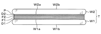
- the wafer processing system 1 as a polymerization substrate in which the first wafer W1 as the first substrate and the second wafer W2 as the second substrate are bonded. Processing is performed on the polymerized wafer T of.
- the first wafer W1 the surface on the side bonded to the second wafer W2 is referred to as the front surface W1a, and the surface opposite to the front surface W1a is referred to as the back surface W1b.
- the front surface W2a the surface on the side joined to the first wafer W1
- the back surface W2b the surface opposite to the front surface W2a
- the first wafer W1 is a semiconductor wafer such as a silicon substrate.
- the device layer D1 and the surface film F1 are laminated on the surface W1a of the first wafer W1 in this order from the surface W1a side.
- the device layer D1 includes a plurality of devices.
- Examples of the surface film F1 include an oxide film (SiO 2 film, TEOS film), a SiC film, a SiCN film, and an adhesive.
- the device layer D1 and the surface film F1 may not be formed on the surface W1a.
- the second wafer W2 is also a semiconductor wafer such as a silicon substrate.
- the laser absorption layer P, the device layer D2, and the surface film F2 are laminated on the surface W2a of the second wafer W2 in this order from the surface W2a side.
- the laser absorption layer P absorbs the laser light emitted from the laser head 110 as described later.
- An oxide film SiO 2 film
- the laser absorption layer P is not particularly limited as long as it absorbs laser light.
- the device layer D2 and the surface film F2 are the same as the device layer D1 and the surface film F1 of the first wafer W1, respectively.
- the surface film F1 of the first wafer W1 and the surface film F2 of the second wafer W2 are joined.
- the position of the laser absorption layer P is not limited to the above embodiment, and may be formed between the device layer D2 and the surface film F2, for example. Further, the device layer D2 and the surface film F2 may not be formed on the surface W2a. In this case, the laser absorption layer P is formed on the first wafer W1 side, and the device layer D1 on the first wafer W1 side is transferred to the second wafer W2 side.
- the wafer processing system 1 has a configuration in which the loading / unloading block 10, the transport block 20, and the processing block 30 are integrally connected.
- the carry-in / out block 10 and the processing block 30 are provided around the transport block 20.
- the carry-in / out block 10 is arranged on the Y-axis negative direction side of the transport block 20.
- the laser irradiation device 31 described later of the processing block 30 is arranged on the negative side of the X-axis of the transport block 20, and the cleaning device 32 described later is arranged on the positive side of the X-axis of the transport block 20.
- cassettes Ct, Cw1 and Cw2 capable of accommodating a plurality of polymerization wafers T, a plurality of first wafers W1 and a plurality of second wafers W2 are carried in / out from the outside.
- the carry-in / out block 10 is provided with a cassette mounting stand 11.
- a plurality of, for example, three cassettes Ct, Cw1 and Cw2 can be freely mounted in a row on the cassette mounting table 11 in the X-axis direction.
- the number of cassettes Ct, Cw1 and Cw2 mounted on the cassette mounting table 11 is not limited to this embodiment and can be arbitrarily determined.
- the transfer block 20 is provided with a wafer transfer device 22 configured to be movable on a transfer path 21 extending in the X-axis direction.
- the wafer transfer device 22 has, for example, two transfer arms 23, 23 that hold and transfer the polymerized wafer T, the first wafer W1, and the second wafer W2.
- Each transport arm 23 is configured to be movable in the horizontal direction, the vertical direction, the horizontal axis, and the vertical axis.
- the configuration of the transport arm 23 is not limited to this embodiment, and any configuration can be adopted.
- the wafer transfer device 22 and the wafer transfer device 22 have the polymer wafer T, the first wafer, with respect to the cassettes Ct, Cw1, Cw2 of the cassette mounting table 11, the laser irradiation device 31 and the cleaning device 32 described later. It is configured to be able to convey W1 and the second wafer W2.
- the processing block 30 has a laser irradiation device 31 and a cleaning device 32.
- the laser irradiation device 31 irradiates the laser absorption layer P of the second wafer W2 with laser light.
- the configuration of the laser irradiation device 31 will be described later.
- the cleaning device 32 cleans the surface of the laser absorption layer P formed on the surface W1a of the first wafer W1 separated by the laser irradiation device 31. For example, a brush is brought into contact with the surface of the laser absorption layer P, and the surface is scrubbed. A pressurized cleaning liquid may be used for cleaning the surface. Further, the cleaning device 32 may have a configuration for cleaning the back surface W1b together with the front surface W1a side of the first wafer W1.
- the above wafer processing system 1 is provided with a control device 40 as a control unit.
- the control device 40 is, for example, a computer and has a program storage unit (not shown).
- the program storage unit stores a program that controls the processing of the polymerized wafer T in the wafer processing system 1. Further, the program storage unit also stores a program for controlling the operation of the drive system of the above-mentioned various processing devices and transfer devices to realize the wafer processing described later in the wafer processing system 1.
- the program may be recorded on a computer-readable storage medium H and may be installed on the control device 40 from the storage medium H.
- the laser irradiation device 31 has a chuck 100 as a holding portion for holding the polymerized wafer T on the upper surface.
- the chuck 100 attracts and holds the entire surface of the back surface W1b of the first wafer W1.
- the chuck 100 may suck and hold a part of the back surface W1b.
- the chuck 100 is provided with an elevating pin (not shown) for supporting and elevating the polymerization wafer T from below.
- the elevating pin is configured to be elevating and lowering by inserting a through hole (not shown) formed through the chuck 100.
- a holding portion (not shown) for holding the second wafer W2 may be provided outside the chuck 100.
- the presence of the non-peeling region B prevents the second wafer W2 from slipping or slipping from the laser absorption layer P, but the slipping or slipping is more reliably prevented by the holding portion. can do.
- the chuck 100 is supported by the slider table 102 via the air bearing 101.
- a rotation mechanism 103 is provided on the lower surface side of the slider table 102.
- the rotation mechanism 103 has, for example, a built-in motor as a drive source.
- the chuck 100 is rotatably configured around the ⁇ axis (vertical axis) by the rotation mechanism 103 via the air bearing 101.
- the slider table 102 is configured to be movable along a rail 105 provided on the base 106 and extending in the Y-axis direction by a moving mechanism 104 provided on the lower surface side thereof.
- the drive source of the moving mechanism 104 is not particularly limited, but for example, a linear motor is used.
- a laser head 110 as a laser irradiation unit is provided above the chuck 100.
- the laser head 110 has a lens 111.
- the lens 111 is a tubular member provided on the lower surface of the laser head 110, and irradiates the polymerized wafer T held by the chuck 100 with laser light.
- the laser beam is a CO 2 laser beam
- the laser beam emitted from the laser head 110 passes through the second wafer W2 and irradiates the laser absorption layer P.
- the wavelength of the CO 2 laser beam is, for example, 8.9 ⁇ m to 11 ⁇ m.
- the laser head 110 is configured to be able to move up and down by an elevating mechanism (not shown).
- the light source of the laser beam is provided at a remote position outside the laser head 110.
- a transport pad 120 as a peeling portion is provided above the chuck 100.
- the transport pad 120 is configured to be able to move up and down by an elevating mechanism (not shown). Further, the transport pad 120 has a suction surface of the second wafer W2. Then, the transfer pad 120 transfers the second wafer W2 between the chuck 100 and the transfer arm 23. Specifically, after moving the chuck 100 to the lower side of the transfer pad 120 (the delivery position with the transfer arm 23), the transfer pad 120 sucks and holds the back surface W2b of the second wafer W2, and the first wafer W1 Peel off from. Subsequently, the peeled second wafer W2 is transferred from the transfer pad 120 to the transfer arm 23 and carried out from the laser irradiation device 31.
- the transfer pad 120 may be configured to invert the front and back surfaces of the wafer by an inversion mechanism (not shown).
- the transfer arm 23 accesses the transfer pad 120 from the positive direction side of the X axis.
- the laser irradiation device 31 shown in FIG. 4 may be rotated 90 degrees counterclockwise, and the transfer arm 23 may access the transfer pad 120 from the negative direction of the Y axis.
- the polymerized wafer T When the polymerized wafer T is carried into the laser irradiation device 31, the polymerized wafer T is delivered from the transport arm 23 to the elevating pin, and is placed on the chuck 100 by lowering the elevating pin. Further, when the peeled first wafer W1 is carried out from the laser irradiation device 31, the polymerized wafer T placed on the chuck 100 is raised by the elevating pin and delivered from the elevating pin to the transfer arm 23.
- the wafer processing performed by using the wafer processing system 1 configured as described above will be described.
- the first wafer W1 and the second wafer W2 are bonded to each other in an external bonding device (not shown) of the wafer processing system 1 to form a polymerized wafer T in advance.
- a cassette Ct containing a plurality of polymerized wafers T is placed on the cassette mounting table 11 of the loading / unloading block 10.
- the polymerized wafer T in the cassette Ct is taken out by the wafer transfer device 22 and transferred to the laser irradiation device 31.
- the laser irradiation device 31 the polymerized wafer T is transferred from the transfer arm 23 to the elevating pin and is attracted and held by the chuck 100.
- the moving mechanism 104 moves the chuck 100 to the processing position.
- This processing position is a position where the laser beam can be irradiated from the laser head 110 to the polymerized wafer T (laser absorption layer P).
- the laser head 110 irradiates the laser absorption layer P with the laser beam L (CO 2 laser beam) in a pulsed manner.
- the laser beam L passes through the second wafer W2 from the back surface W2b side of the second wafer W2 and is absorbed by the laser absorption layer P.
- the laser beam L causes peeling at the interface between the laser absorption layer P and the second wafer W2. Almost all the laser light L is absorbed by the laser absorption layer P and does not reach the device layer D2. Therefore, it is possible to prevent the device layer D2 from being damaged.
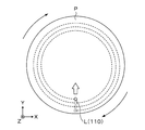
- the rotation mechanism 103 rotates the chuck 100 (polymerized wafer T), and the movement mechanism 104 moves the chuck 100 in the Y-axis direction. Then, the laser beam L is irradiated to the laser absorption layer P from the outer side to the inner side in the radial direction, and as a result, is spirally irradiated from the outer side to the inner side.
- the black arrow shown in FIG. 6 indicates the rotation direction of the chuck 100.
- the irradiation start position of the laser beam L is preferably between the outer peripheral edge Ea of the second wafer W2 and the junction end Eb of the first wafer W1 and the second wafer W2 in the polymerization wafer T.
- the eccentricity is absorbed and the laser beam L is applied to the laser absorption layer P. It can be irradiated appropriately.
- the laser beam L may be irradiated concentrically in an annular shape.
- the rotation of the chuck 100 and the Y direction of the chuck 100 are alternately performed, it is better to irradiate the laser beam L in a spiral shape as described above to shorten the irradiation time and improve the throughput. Can be done.
- the laser beam L may be irradiated from the inside to the outside in the radial direction.
- the stress due to the peeling may be directed outward in the radial direction, and the portion outside which the laser beam L is not irradiated may also be peeled off.
- the stress associated with the peeling can be released to the outside, so that the peeling can be controlled more easily. Further, by appropriately controlling the peeling, it is possible to suppress the roughness of the peeled surface.
- the chuck 100 when the laser absorption layer P is irradiated with the laser beam L, the chuck 100 is rotated, but the laser head 110 is moved and the laser head 110 is rotated relative to the chuck 100. May be good. Further, although the chuck 100 is moved in the Y-axis direction, the laser head 110 may be moved in the Y-axis direction.
- the chuck 100 rotates, so that the second wafer W2 is subjected to. Centrifugal force acts to cause the second wafer W2 to shift from the laser absorption layer P, and the laser beam L may be irradiated to a place other than the processing target position during the laser processing. In addition, the second wafer W2 may slide off the chuck 100.
- a peeling region A and a non-peeling region B are formed in the laser absorption layer P as shown in FIG.
- the peeling region A is a region to which the laser beam L is irradiated, and in this peeling region A, peeling occurs at the interface between the laser absorption layer P and the second wafer W2.
- the non-peeling region B is a region not irradiated with the laser beam L, and in this non-peeling region B, peeling does not occur at the interface between the laser absorption layer P and the second wafer W2, and the laser absorption layer P and the non-peeling region B The second wafer W2 is joined.
- the laser beam L can be irradiated to an appropriate position.
- the irradiation of the laser beam L from the laser head 110 may be stopped at the position where the non-peeling region B is to be formed.
- non-peeling regions B are formed at the central portion of the laser absorption layer P and four peripheral edges thereof, but the positions and numbers of the non-peeling regions B are arbitrary.
- the non-peelable region B may be formed to such an extent that the second wafer W2 does not shift or slide down.
- the range of the peeling region A is set to the non-peeling region B in order to prevent a large load from being applied. Make it larger than the range.
- the laser irradiation device 31 irradiates the laser beam L in a pulse shape so that the peeling region A and the non-peeling region B are formed on the laser absorbing layer P.
- the cause of the peeling is not the energy amount of the laser beam L but the peak power (maximum intensity of the laser beam).
- the laser beam L is continuously oscillated (when a continuous wave is used), it is difficult to increase the peak power, and peeling may not occur.
- the laser beam L when the laser beam L is oscillated in a pulse shape (when a pulse wave is used), the peak power can be increased to cause peeling at the interface between the laser absorption layer P and the second wafer W2. , The second wafer W2 can be appropriately peeled from the laser absorption layer P.
- the laser beam obtained by oscillating the CO 2 laser in a pulse shape is a so-called pulse laser, and its power repeats 0 (zero) and the maximum value.
- the chuck 100 is moved to the delivery position by the moving mechanism 104.
- an inertial force acts on the second wafer W2, and the second wafer W2 may be displaced from the laser absorption layer P.
- the back surface W2b of the second wafer W2 is subsequently sucked and held by the transport pad 120, an appropriate position cannot be sucked and held.
- the non-peelable region B is formed in the laser absorption layer P, it is possible to prevent the second wafer W2 from shifting.
- the transfer pad 120 sucks and holds the back surface W2b of the second wafer W2. Then, as shown in FIG. 9B, with the transport pad 120 adsorbing and holding the second wafer W2, the transport pad 120 is raised to peel the second wafer W2 from the laser absorption layer P. At this time, since the non-peeling region B is formed in the laser absorbing layer P, a load is applied to the extent that the second wafer W2 can be peeled from the laser absorbing layer P in this non-peeling region B. Then, the second wafer W2 can be peeled from the laser absorption layer P.
- the transfer pad 120 may be rotated around the vertical axis to peel off the second wafer W2.
- the peeled second wafer W2 is delivered from the transfer pad 120 to the transfer arm 23 of the wafer transfer device 22, and is transferred to the cassette Cw2 of the cassette mounting table 11.
- the second wafer W2 carried out from the laser irradiation device 31 may be conveyed to the cleaning device 32 before being conveyed to the cassette Cw2, and the surface W2a which is the peeling surface thereof may be cleaned.
- the front and back surfaces of the second wafer W2 may be inverted by the transfer pad 120 and transferred to the transfer arm 23.
- the first wafer W1 held by the chuck 100 is raised from the chuck 100 by the elevating pin, delivered to the transport arm 23, and transported to the cleaning device 32.
- the surface of the laser absorption layer P which is the peeling surface, is scrubbed.
- the back surface W1b of the first wafer W1 may be cleaned together with the front surface of the laser absorption layer P.
- a cleaning unit for cleaning the front surface of the laser absorption layer P and the back surface W1b of the first wafer W1 may be provided separately.
- the first wafer W1 that has been subjected to all the processing is transferred to the cassette Cw1 of the cassette mounting table 11 by the wafer transfer device 22. In this way, a series of wafer processing in the wafer processing system 1 is completed.
- the non-peeling region B when the laser beam L is spirally irradiated from the radial outside to the inside of the laser absorption layer P, the non-peeling region B is formed, so that even if the chuck 100 is rotated, the second It is possible to prevent the wafer W2 from slipping or slipping. Further, even when the chuck 100 moves after the irradiation with the laser beam L, the non-peeling region B can prevent the second wafer W2 from shifting. Therefore, the second wafer W2 can be appropriately peeled from the laser absorption layer P, and the device layer D2 can be transferred to the first wafer W1.
- the laser absorption layer P is irradiated with the laser beam L in a spiral or concentric pattern, but the irradiation pattern of the laser beam L is not limited to this.
- the configuration of the device corresponding to such various irradiation patterns is not limited to the laser irradiation device 31 of the above embodiment.
- the chuck 100 is rotatable around the ⁇ axis and movable in the uniaxial (Y axis) direction, but may be moved in two axes (X axis and Y axis).
- a galvano may be used for the laser head 110, and the laser light L emitted from the laser head 110 may be scanned against the laser absorption layer P.
- the laser beam L is scanned in a predetermined scanning range of the laser absorption layer P.
- the chuck 100 is moved in the X-axis direction while the irradiation of the laser beam L is stopped. In this way, the irradiation and scanning of the laser beam L and the movement of the chuck 100 are repeatedly performed to irradiate the laser beam L in a row in the X-axis direction.
- the chuck 100 is moved so as to be displaced in the Y-axis direction, and the irradiation and scanning of the laser beam L and the movement of the chuck 100 are repeatedly performed in the same manner as described above to irradiate the laser beam L in a row in the X-axis direction. To do. Then, the laser beam L is applied to the laser absorption layer P.
- the irradiation and scanning of the laser beam L and the movement of the chuck 100 were repeatedly performed, but the irradiation and scanning of the laser beam L and the movement of the chuck 100 were performed while moving the chuck 100 in a row in the X-axis direction. Scanning may be performed. Then, after irradiating the laser beam L in a row in the X-axis direction, the chuck 100 is moved so as to be displaced in the Y-axis direction, and the laser beam L is irradiated to the laser absorption layer P.
- the irradiation of the spiral (or concentric) laser beam L of the above embodiment may be combined with the irradiation and scanning of the laser beam L.
- the rotation speed of the chuck 100 increases as the laser beam L moves from the outer side to the inner side in the radial direction. Therefore, on the outer peripheral portion of the laser absorption layer P, the chuck 100 is moved from the outside in the radial direction to the inside while rotating the chuck 100, and the laser beam L is spirally irradiated. Then, when the rotation speed of the chuck 100 reaches the upper limit, the rotation of the chuck 100 is stopped at the central portion of the laser absorption layer P, and scanning is performed while irradiating the laser beam L.
- the laser beam L is prevented from overlapping, and the interval of irradiating the laser beam L, that is, the interval of the pulse is made constant. can do.
- the first wafer W1 and the second wafer W2 can be uniformly peeled off in the wafer surface.
- the wafer processing system 1 of the above embodiment has a cleaning device 32, but the wafer processing system 1 may further have an etching device (not shown).
- the etching apparatus etches the surface W1a of the first wafer W1 after peeling, specifically, the surface of the laser absorption layer P.
- a chemical solution etching solution
- the wafer processing system 1 may have either a cleaning device 32 or an etching device.
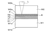
- a reflective film R may be provided between the laser absorption layer P and the device layer D2 as shown in FIG. That is, the reflective film R is formed on the surface of the laser absorbing layer P opposite to the incident surface of the laser beam L.
- a material having a high reflectance to the laser beam L and a high melting point for example, a metal film is used.
- the device layer D2 is a layer having a function and is different from the reflective film R.
- the laser beam L emitted from the laser head 110 passes through the second wafer W2 and is almost completely absorbed by the laser absorption layer P, but even if there is a laser beam L that cannot be completely absorbed. It is reflected by the reflective film R. As a result, the laser beam L does not reach the device layer D2, and it is possible to reliably suppress the device layer D2 from being damaged.
- the laser beam L reflected by the reflective film R is absorbed by the laser absorption layer P. Therefore, the peeling efficiency of the second wafer W2 can be improved.
- Laser irradiation device 40 Control device 100 Chuck 110 Laser head 120 Conveyor pad A Peeling area B Non-peeling area D1, D2 Device layer P Laser absorption layer T Polymerized wafer W1 First wafer W2 Second wafer
Landscapes
- Physics & Mathematics (AREA)
- Optics & Photonics (AREA)
- Engineering & Computer Science (AREA)
- Chemical & Material Sciences (AREA)
- Chemical Kinetics & Catalysis (AREA)
- General Chemical & Material Sciences (AREA)
- Oil, Petroleum & Natural Gas (AREA)
- Plasma & Fusion (AREA)
- Mechanical Engineering (AREA)
- Container, Conveyance, Adherence, Positioning, Of Wafer (AREA)
- Laser Beam Processing (AREA)
Priority Applications (2)
| Application Number | Priority Date | Filing Date | Title |
|---|---|---|---|
| JP2021567195A JP7308292B2 (ja) | 2019-12-26 | 2020-12-09 | 基板処理装置及び基板処理方法 |
| CN202080086729.9A CN114830293A (zh) | 2019-12-26 | 2020-12-09 | 基板处理装置和基板处理方法 |
Applications Claiming Priority (2)
| Application Number | Priority Date | Filing Date | Title |
|---|---|---|---|
| JP2019236287 | 2019-12-26 | ||
| JP2019-236287 | 2019-12-26 |
Publications (1)
| Publication Number | Publication Date |
|---|---|
| WO2021131710A1 true WO2021131710A1 (ja) | 2021-07-01 |
Family
ID=76575478
Family Applications (1)
| Application Number | Title | Priority Date | Filing Date |
|---|---|---|---|
| PCT/JP2020/045883 Ceased WO2021131710A1 (ja) | 2019-12-26 | 2020-12-09 | 基板処理装置及び基板処理方法 |
Country Status (3)
| Country | Link |
|---|---|
| JP (1) | JP7308292B2 (https=) |
| CN (1) | CN114830293A (https=) |
| WO (1) | WO2021131710A1 (https=) |
Cited By (1)
| Publication number | Priority date | Publication date | Assignee | Title |
|---|---|---|---|---|
| WO2025009324A1 (ja) * | 2023-07-05 | 2025-01-09 | 東京エレクトロン株式会社 | 処理システム及び処理方法 |
Families Citing this family (1)
| Publication number | Priority date | Publication date | Assignee | Title |
|---|---|---|---|---|
| JP7690038B2 (ja) * | 2021-09-06 | 2025-06-09 | 東京エレクトロン株式会社 | 基板処理方法及び基板処理装置 |
Citations (5)
| Publication number | Priority date | Publication date | Assignee | Title |
|---|---|---|---|---|
| JPH10125929A (ja) * | 1996-08-27 | 1998-05-15 | Seiko Epson Corp | 剥離方法 |
| JP2013179237A (ja) * | 2012-02-29 | 2013-09-09 | Disco Abrasive Syst Ltd | リフトオフ装置 |
| JP2013239650A (ja) * | 2012-05-16 | 2013-11-28 | Tokyo Ohka Kogyo Co Ltd | 支持体分離方法および支持体分離装置 |
| JP2015144192A (ja) * | 2014-01-31 | 2015-08-06 | 株式会社ディスコ | リフトオフ方法 |
| JP2017084910A (ja) * | 2015-10-26 | 2017-05-18 | 東京応化工業株式会社 | 支持体分離方法 |
Family Cites Families (2)
| Publication number | Priority date | Publication date | Assignee | Title |
|---|---|---|---|---|
| JP6450637B2 (ja) * | 2015-04-21 | 2019-01-09 | 株式会社ディスコ | リフトオフ方法及び超音波ホーン |
| CN106910678B (zh) * | 2017-03-09 | 2019-05-21 | 华中科技大学 | 图案化掩膜版、其制备方法及使用其进行激光剥离的方法 |
-
2020
- 2020-12-09 CN CN202080086729.9A patent/CN114830293A/zh active Pending
- 2020-12-09 WO PCT/JP2020/045883 patent/WO2021131710A1/ja not_active Ceased
- 2020-12-09 JP JP2021567195A patent/JP7308292B2/ja active Active
Patent Citations (5)
| Publication number | Priority date | Publication date | Assignee | Title |
|---|---|---|---|---|
| JPH10125929A (ja) * | 1996-08-27 | 1998-05-15 | Seiko Epson Corp | 剥離方法 |
| JP2013179237A (ja) * | 2012-02-29 | 2013-09-09 | Disco Abrasive Syst Ltd | リフトオフ装置 |
| JP2013239650A (ja) * | 2012-05-16 | 2013-11-28 | Tokyo Ohka Kogyo Co Ltd | 支持体分離方法および支持体分離装置 |
| JP2015144192A (ja) * | 2014-01-31 | 2015-08-06 | 株式会社ディスコ | リフトオフ方法 |
| JP2017084910A (ja) * | 2015-10-26 | 2017-05-18 | 東京応化工業株式会社 | 支持体分離方法 |
Cited By (1)
| Publication number | Priority date | Publication date | Assignee | Title |
|---|---|---|---|---|
| WO2025009324A1 (ja) * | 2023-07-05 | 2025-01-09 | 東京エレクトロン株式会社 | 処理システム及び処理方法 |
Also Published As
| Publication number | Publication date |
|---|---|
| JPWO2021131710A1 (https=) | 2021-07-01 |
| JP7308292B2 (ja) | 2023-07-13 |
| CN114830293A (zh) | 2022-07-29 |
| TW202129742A (zh) | 2021-08-01 |
Similar Documents
| Publication | Publication Date | Title |
|---|---|---|
| JP7304433B2 (ja) | 基板処理方法及び基板処理装置 | |
| JP7386077B2 (ja) | 基板処理装置及び基板処理方法 | |
| TWI871441B (zh) | 基板處理方法及基板處理裝置 | |
| WO2021192853A1 (ja) | 基板処理方法及び基板処理装置 | |
| WO2021131710A1 (ja) | 基板処理装置及び基板処理方法 | |
| TWI913238B (zh) | 基板處理裝置及基板處理方法 | |
| JP2022091504A (ja) | レーザ照射システム、基板処理装置及び基板処理方法 |
Legal Events
| Date | Code | Title | Description |
|---|---|---|---|
| 121 | Ep: the epo has been informed by wipo that ep was designated in this application |
Ref document number: 20905564 Country of ref document: EP Kind code of ref document: A1 |
|
| ENP | Entry into the national phase |
Ref document number: 2021567195 Country of ref document: JP Kind code of ref document: A |
|
| NENP | Non-entry into the national phase |
Ref country code: DE |
|
| 122 | Ep: pct application non-entry in european phase |
Ref document number: 20905564 Country of ref document: EP Kind code of ref document: A1 |