WO2021100126A1 - 半導体装置 - Google Patents
半導体装置 Download PDFInfo
- Publication number
- WO2021100126A1 WO2021100126A1 PCT/JP2019/045298 JP2019045298W WO2021100126A1 WO 2021100126 A1 WO2021100126 A1 WO 2021100126A1 JP 2019045298 W JP2019045298 W JP 2019045298W WO 2021100126 A1 WO2021100126 A1 WO 2021100126A1
- Authority
- WO
- WIPO (PCT)
- Prior art keywords
- conductor layer
- inner conductor
- circuit board
- peripheral edge
- thin
- Prior art date
- Legal status (The legal status is an assumption and is not a legal conclusion. Google has not performed a legal analysis and makes no representation as to the accuracy of the status listed.)
- Ceased
Links
Images



Classifications
-
- H—ELECTRICITY
- H10—SEMICONDUCTOR DEVICES; ELECTRIC SOLID-STATE DEVICES NOT OTHERWISE PROVIDED FOR
- H10W—GENERIC PACKAGES, INTERCONNECTIONS, CONNECTORS OR OTHER CONSTRUCTIONAL DETAILS OF DEVICES COVERED BY CLASS H10
- H10W70/00—Package substrates; Interposers; Redistribution layers [RDL]
- H10W70/60—Insulating or insulated package substrates; Interposers; Redistribution layers
- H10W70/67—Insulating or insulated package substrates; Interposers; Redistribution layers characterised by their insulating layers or insulating parts
- H10W70/68—Shapes or dispositions thereof
-
- H—ELECTRICITY
- H10—SEMICONDUCTOR DEVICES; ELECTRIC SOLID-STATE DEVICES NOT OTHERWISE PROVIDED FOR
- H10W—GENERIC PACKAGES, INTERCONNECTIONS, CONNECTORS OR OTHER CONSTRUCTIONAL DETAILS OF DEVICES COVERED BY CLASS H10
- H10W76/00—Containers; Fillings or auxiliary members therefor; Seals
- H10W76/10—Containers or parts thereof
- H10W76/12—Containers or parts thereof characterised by their shape
- H10W76/13—Containers comprising a conductive base serving as an interconnection
- H10W76/138—Containers comprising a conductive base serving as an interconnection having another interconnection being formed by a cover plate parallel to the conductive base, e.g. sandwich type
-
- H—ELECTRICITY
- H10—SEMICONDUCTOR DEVICES; ELECTRIC SOLID-STATE DEVICES NOT OTHERWISE PROVIDED FOR
- H10W—GENERIC PACKAGES, INTERCONNECTIONS, CONNECTORS OR OTHER CONSTRUCTIONAL DETAILS OF DEVICES COVERED BY CLASS H10
- H10W70/00—Package substrates; Interposers; Redistribution layers [RDL]
- H10W70/40—Leadframes
- H10W70/464—Additional interconnections in combination with leadframes
- H10W70/468—Circuit boards
-
- H—ELECTRICITY
- H10—SEMICONDUCTOR DEVICES; ELECTRIC SOLID-STATE DEVICES NOT OTHERWISE PROVIDED FOR
- H10W—GENERIC PACKAGES, INTERCONNECTIONS, CONNECTORS OR OTHER CONSTRUCTIONAL DETAILS OF DEVICES COVERED BY CLASS H10
- H10W70/00—Package substrates; Interposers; Redistribution layers [RDL]
- H10W70/40—Leadframes
- H10W70/479—Leadframes on or in insulating or insulated package substrates, interposers, or redistribution layers
-
- H—ELECTRICITY
- H10—SEMICONDUCTOR DEVICES; ELECTRIC SOLID-STATE DEVICES NOT OTHERWISE PROVIDED FOR
- H10W—GENERIC PACKAGES, INTERCONNECTIONS, CONNECTORS OR OTHER CONSTRUCTIONAL DETAILS OF DEVICES COVERED BY CLASS H10
- H10W70/00—Package substrates; Interposers; Redistribution layers [RDL]
- H10W70/40—Leadframes
- H10W70/481—Leadframes for devices being provided for in groups H10D8/00 - H10D48/00
-
- H—ELECTRICITY
- H10—SEMICONDUCTOR DEVICES; ELECTRIC SOLID-STATE DEVICES NOT OTHERWISE PROVIDED FOR
- H10W—GENERIC PACKAGES, INTERCONNECTIONS, CONNECTORS OR OTHER CONSTRUCTIONAL DETAILS OF DEVICES COVERED BY CLASS H10
- H10W70/00—Package substrates; Interposers; Redistribution layers [RDL]
- H10W70/60—Insulating or insulated package substrates; Interposers; Redistribution layers
- H10W70/67—Insulating or insulated package substrates; Interposers; Redistribution layers characterised by their insulating layers or insulating parts
- H10W70/68—Shapes or dispositions thereof
- H10W70/685—Shapes or dispositions thereof comprising multiple insulating layers
-
- H—ELECTRICITY
- H10—SEMICONDUCTOR DEVICES; ELECTRIC SOLID-STATE DEVICES NOT OTHERWISE PROVIDED FOR
- H10W—GENERIC PACKAGES, INTERCONNECTIONS, CONNECTORS OR OTHER CONSTRUCTIONAL DETAILS OF DEVICES COVERED BY CLASS H10
- H10W74/00—Encapsulations, e.g. protective coatings
- H10W74/10—Encapsulations, e.g. protective coatings characterised by their shape or disposition
- H10W74/111—Encapsulations, e.g. protective coatings characterised by their shape or disposition the semiconductor body being completely enclosed
- H10W74/114—Encapsulations, e.g. protective coatings characterised by their shape or disposition the semiconductor body being completely enclosed by a substrate and the encapsulations
-
- H—ELECTRICITY
- H10—SEMICONDUCTOR DEVICES; ELECTRIC SOLID-STATE DEVICES NOT OTHERWISE PROVIDED FOR
- H10W—GENERIC PACKAGES, INTERCONNECTIONS, CONNECTORS OR OTHER CONSTRUCTIONAL DETAILS OF DEVICES COVERED BY CLASS H10
- H10W90/00—Package configurations
- H10W90/401—Package configurations characterised by multiple insulating or insulated package substrates, interposers or RDLs
-
- H—ELECTRICITY
- H10—SEMICONDUCTOR DEVICES; ELECTRIC SOLID-STATE DEVICES NOT OTHERWISE PROVIDED FOR
- H10W—GENERIC PACKAGES, INTERCONNECTIONS, CONNECTORS OR OTHER CONSTRUCTIONAL DETAILS OF DEVICES COVERED BY CLASS H10
- H10W90/00—Package configurations
- H10W90/811—Multiple chips on leadframes
-
- H—ELECTRICITY
- H10—SEMICONDUCTOR DEVICES; ELECTRIC SOLID-STATE DEVICES NOT OTHERWISE PROVIDED FOR
- H10W—GENERIC PACKAGES, INTERCONNECTIONS, CONNECTORS OR OTHER CONSTRUCTIONAL DETAILS OF DEVICES COVERED BY CLASS H10
- H10W40/00—Arrangements for thermal protection or thermal control
- H10W40/20—Arrangements for cooling
- H10W40/25—Arrangements for cooling characterised by their materials
- H10W40/255—Arrangements for cooling characterised by their materials having a laminate or multilayered structure, e.g. direct bond copper [DBC] ceramic substrates
-
- H—ELECTRICITY
- H10—SEMICONDUCTOR DEVICES; ELECTRIC SOLID-STATE DEVICES NOT OTHERWISE PROVIDED FOR
- H10W—GENERIC PACKAGES, INTERCONNECTIONS, CONNECTORS OR OTHER CONSTRUCTIONAL DETAILS OF DEVICES COVERED BY CLASS H10
- H10W70/00—Package substrates; Interposers; Redistribution layers [RDL]
- H10W70/60—Insulating or insulated package substrates; Interposers; Redistribution layers
- H10W70/611—Insulating or insulated package substrates; Interposers; Redistribution layers for connecting multiple chips together
-
- H—ELECTRICITY
- H10—SEMICONDUCTOR DEVICES; ELECTRIC SOLID-STATE DEVICES NOT OTHERWISE PROVIDED FOR
- H10W—GENERIC PACKAGES, INTERCONNECTIONS, CONNECTORS OR OTHER CONSTRUCTIONAL DETAILS OF DEVICES COVERED BY CLASS H10
- H10W70/00—Package substrates; Interposers; Redistribution layers [RDL]
- H10W70/60—Insulating or insulated package substrates; Interposers; Redistribution layers
- H10W70/62—Insulating or insulated package substrates; Interposers; Redistribution layers characterised by their interconnections
- H10W70/65—Shapes or dispositions of interconnections
- H10W70/658—Shapes or dispositions of interconnections for devices provided for in groups H10D8/00 - H10D48/00
-
- H—ELECTRICITY
- H10—SEMICONDUCTOR DEVICES; ELECTRIC SOLID-STATE DEVICES NOT OTHERWISE PROVIDED FOR
- H10W—GENERIC PACKAGES, INTERCONNECTIONS, CONNECTORS OR OTHER CONSTRUCTIONAL DETAILS OF DEVICES COVERED BY CLASS H10
- H10W72/00—Interconnections or connectors in packages
- H10W72/071—Connecting or disconnecting
- H10W72/073—Connecting or disconnecting of die-attach connectors
- H10W72/07351—Connecting or disconnecting of die-attach connectors characterised by changes in properties of the die-attach connectors during connecting
- H10W72/07354—Connecting or disconnecting of die-attach connectors characterised by changes in properties of the die-attach connectors during connecting changes in dispositions
-
- H—ELECTRICITY
- H10—SEMICONDUCTOR DEVICES; ELECTRIC SOLID-STATE DEVICES NOT OTHERWISE PROVIDED FOR
- H10W—GENERIC PACKAGES, INTERCONNECTIONS, CONNECTORS OR OTHER CONSTRUCTIONAL DETAILS OF DEVICES COVERED BY CLASS H10
- H10W72/00—Interconnections or connectors in packages
- H10W72/30—Die-attach connectors
- H10W72/341—Dispositions of die-attach connectors, e.g. layouts
- H10W72/347—Dispositions of multiple die-attach connectors
-
- H—ELECTRICITY
- H10—SEMICONDUCTOR DEVICES; ELECTRIC SOLID-STATE DEVICES NOT OTHERWISE PROVIDED FOR
- H10W—GENERIC PACKAGES, INTERCONNECTIONS, CONNECTORS OR OTHER CONSTRUCTIONAL DETAILS OF DEVICES COVERED BY CLASS H10
- H10W72/00—Interconnections or connectors in packages
- H10W72/851—Dispositions of multiple connectors or interconnections
- H10W72/874—On different surfaces
- H10W72/877—Bump connectors and die-attach connectors
-
- H—ELECTRICITY
- H10—SEMICONDUCTOR DEVICES; ELECTRIC SOLID-STATE DEVICES NOT OTHERWISE PROVIDED FOR
- H10W—GENERIC PACKAGES, INTERCONNECTIONS, CONNECTORS OR OTHER CONSTRUCTIONAL DETAILS OF DEVICES COVERED BY CLASS H10
- H10W74/00—Encapsulations, e.g. protective coatings
-
- H—ELECTRICITY
- H10—SEMICONDUCTOR DEVICES; ELECTRIC SOLID-STATE DEVICES NOT OTHERWISE PROVIDED FOR
- H10W—GENERIC PACKAGES, INTERCONNECTIONS, CONNECTORS OR OTHER CONSTRUCTIONAL DETAILS OF DEVICES COVERED BY CLASS H10
- H10W90/00—Package configurations
-
- H—ELECTRICITY
- H10—SEMICONDUCTOR DEVICES; ELECTRIC SOLID-STATE DEVICES NOT OTHERWISE PROVIDED FOR
- H10W—GENERIC PACKAGES, INTERCONNECTIONS, CONNECTORS OR OTHER CONSTRUCTIONAL DETAILS OF DEVICES COVERED BY CLASS H10
- H10W90/00—Package configurations
- H10W90/701—Package configurations characterised by the relative positions of pads or connectors relative to package parts
- H10W90/721—Package configurations characterised by the relative positions of pads or connectors relative to package parts of bump connectors
- H10W90/724—Package configurations characterised by the relative positions of pads or connectors relative to package parts of bump connectors between a chip and a stacked insulating package substrate, interposer or RDL
-
- H—ELECTRICITY
- H10—SEMICONDUCTOR DEVICES; ELECTRIC SOLID-STATE DEVICES NOT OTHERWISE PROVIDED FOR
- H10W—GENERIC PACKAGES, INTERCONNECTIONS, CONNECTORS OR OTHER CONSTRUCTIONAL DETAILS OF DEVICES COVERED BY CLASS H10
- H10W90/00—Package configurations
- H10W90/701—Package configurations characterised by the relative positions of pads or connectors relative to package parts
- H10W90/731—Package configurations characterised by the relative positions of pads or connectors relative to package parts of die-attach connectors
- H10W90/734—Package configurations characterised by the relative positions of pads or connectors relative to package parts of die-attach connectors between a chip and a stacked insulating package substrate, interposer or RDL
Definitions
- the technology disclosed herein relates to semiconductor devices.
- the insulating circuit board is a board provided with conductor layers (for example, metal plates) on both sides of an insulator board (for example, a ceramic substrate).
- Typical examples of the insulated circuit board include, but are not limited to, a DBC (Direct Bonded Copper) board, a DBA (Direct Bonded Aluminum) board, and an AMB (Active Metal brazed Copper) board.
- An insulated circuit board is disclosed in Japanese Patent Application Laid-Open No. 01-059986.
- This insulating circuit board has a ceramic substrate, an inner conductor layer provided on one side of the ceramic substrate, and an outer conductor layer provided on the other side of the ceramic substrate.
- Each of the inner conductor layer and the outer conductor layer has a thin-walled portion formed along the outer peripheral edge thereof, whereby the residual stress generated in the ceramic substrate is reduced.
- the following semiconductor devices can be realized using an insulated circuit board.
- This semiconductor device includes an insulating circuit board, a semiconductor element arranged on the insulating circuit board, and a sealant for sealing the semiconductor element.
- the inner conductor layer is electrically connected to the electrodes of the semiconductor element inside the encapsulant.
- the outer conductor layer is exposed on the surface of the encapsulant and releases the heat of the semiconductor element to the outside.
- the sealing body is formed thinly at the portion covering the thin-walled portion, so that the sealing body is likely to be peeled off at that position.
- the semiconductor device disclosed in the present specification includes a first insulated circuit board, a semiconductor element arranged on the first insulated circuit board, and a sealant for sealing the semiconductor element.
- the first insulating circuit board includes a first insulator substrate, a first inner conductor layer provided on one side of the first insulator substrate, and a first outer conductor layer provided on the other side of the first insulator substrate. And have.
- the first inner conductor layer is electrically connected to the first electrode of the semiconductor element inside the encapsulant.
- the first outer conductor layer is exposed on the surface of the encapsulant.
- a thin-walled portion whose thickness decreases toward the outside is formed with a first width along the outer peripheral edge thereof.
- the first outer conductor layer does not have a thin portion whose thickness decreases toward the outside.
- the first outer conductor layer is formed with a thin-walled portion whose thickness decreases toward the outside with a second width smaller than the first width along the outer peripheral edge thereof.
- the first inner conductor layer of the first insulating circuit board is located inside the encapsulant. According to such a configuration, the thermal stress generated in the sealing body tends to increase locally in the vicinity of the outer peripheral edge of the first inner conductor layer. However, since a thin portion is formed on the outer peripheral edge of the first inner conductor layer, such concentration of thermal stress can be relaxed. On the other hand, the first outer conductor layer of the first insulating circuit board is exposed on the surface of the encapsulant. In this case, as described above, if the thin-walled portion is provided on the outer peripheral edge of the first outer conductor layer, the sealed body is likely to be peeled off at the position of the thin-walled portion. Therefore, there is no thin-walled portion on the outer peripheral edge of the first outer conductor layer, or the thin-walled portion is formed with a small width, and peeling of the sealed body is suppressed.
- FIG. 2 is a cross-sectional view taken along the line II-II in FIG.
- FIG. 3 is a cross-sectional view taken along the line III-III in FIG.
- the thickness of the first inner conductor layer may be larger than the thickness of the first outer conductor layer. According to such a configuration, the heat capacity of the first inner conductor layer close to the semiconductor element is increased, and the temperature change of the semiconductor element is suppressed.
- the surface of the first inner conductor layer may have an inclined surface that is inclined at a constant inclination angle.
- the inclination angle referred to here means an angle formed by the inclined surface and the surface of the insulator substrate, and the larger the inclined angle of the inclined surface, the larger the rate of change in the thickness in the thin-walled portion.
- the surface of the first inner conductor layer may have two or more inclined surfaces having different inclination angles.
- the inclination angle is not particularly limited, but it is preferable that the inclination angle is larger as the inclination surface is located on the outer side.
- the thin portion of the first inner conductor layer may have a curved surface in which the surface of the first inner conductor layer is curved in a convex or concave shape.
- the inclined surface and the second inclined surface may be a part of the curved surface or may be a plane different from the curved surface.
- the outer peripheral edge of the first inner conductor layer may be located outside the outer peripheral edge of the first outer conductor layer. According to such a configuration, the heat capacity of the first inner conductor layer close to the semiconductor element is increased, and the temperature change of the semiconductor element is suppressed.
- the inner peripheral edge of the thin-walled portion of the first inner conductor layer is located inside the inner peripheral edge of the thin-walled portion of the first outer conductor layer. May be good. According to such a configuration, the width of the thin portion of the first inner conductor layer (that is, the first width) is increased, and the concentration of thermal stress generated in the sealing body is effectively relaxed.
- the semiconductor device may further include a second insulated circuit board facing the first insulated circuit board via a semiconductor element.
- the second insulating circuit board includes a second insulator substrate, a second inner conductor layer provided on one side of the second insulator substrate, and a second insulating circuit board provided on the other side of the second insulator substrate. It may have an outer conductor layer.
- the second inner conductor layer may be electrically connected to the second electrode of the semiconductor element inside the encapsulant.
- the second outer conductor layer may be exposed to the other surface of the encapsulant.
- a thin portion whose thickness decreases toward the outside may be formed with a third width along the outer peripheral edge thereof.
- the second outer conductor layer may not have a thin portion whose thickness decreases toward the outside.
- the second outer conductor layer may be formed with a thin portion whose thickness decreases toward the outside with a fourth width smaller than the third width along the outer peripheral edge thereof. According to such a configuration, the same effect as that of the first insulated circuit board described above can be obtained for the second insulated circuit board.
- the inner peripheral edge of the thin-walled portion of the first inner conductor layer is larger than the inner peripheral edge of the thin-walled portion of the second inner conductor layer. It may be located on the outside.
- the thermal stress generated in the encapsulant tends to increase particularly in the vicinity of the inner peripheral edge of the thin portion of each inner conductor layer. Therefore, it is preferable that the two inner peripheral edges are not close to each other, and by being offset from each other, the concentration of thermal stress generated in the sealing body can be suppressed.
- the inner peripheral edge of the thin-walled portion of the first inner conductor layer is located outside the outer peripheral edge of the second inner conductor layer. You may. According to such a configuration, since the inner peripheral edges of the two inner conductor layers are arranged further apart, the concentration of thermal stress generated in the encapsulant can be further suppressed.
- the semiconductor element may be a switching element that conducts and cuts off between the first electrode and the second electrode.
- the switching element is not particularly limited, but may be an IGBT (Insulated Gate Bipolar Transistor) or a MOSFET (Metal-Oxide-Semiconductor Field-Effect Transistor).
- the semiconductor device 10 of the embodiment will be described with reference to the drawings.
- the semiconductor device 10 is adopted in, for example, a power control device for an electric vehicle, and can form at least a part of a power conversion circuit such as a converter or an inverter.
- the term "electric vehicle” as used herein broadly means an vehicle having a motor for driving wheels. For example, an electric vehicle charged by an external electric power, a hybrid vehicle having an engine in addition to a motor, and a fuel cell-powered fuel. Including battery cars, etc.
- the semiconductor device 10 includes a first semiconductor element 12, a second semiconductor element 14, and a sealing body 52.
- the first semiconductor element 12 and the second semiconductor element 14 are sealed inside the sealing body 52.
- the sealing body 52 is made of an insulating material.
- the sealing body 52 in this embodiment is made of a thermosetting resin such as an epoxy resin.
- the sealing body 52 generally has a plate shape, and has an upper surface 52a and a lower surface 52b located on the opposite side of the upper surface 52a.
- the first semiconductor element 12 has a semiconductor substrate 12a, an upper surface electrode 12b, a lower surface electrode 12c, and a plurality of signal electrodes 12d.
- the upper surface electrode 12b and the plurality of signal electrodes 12d are located on the upper surface of the semiconductor substrate 12a, and the lower surface electrode 12c is located on the lower surface of the semiconductor substrate 12a.
- the first semiconductor element 12 is a switching element that conducts and cuts off between the upper surface electrode 12b and the lower surface electrode 12c, and is specifically an RC-IGBT. That is, the first semiconductor element 12 has a built-in freewheeling diode in addition to the IGBT.
- the first semiconductor element 12 may be a MOSFET or another type of semiconductor element.
- the second semiconductor element 14 has a semiconductor substrate 14a, an upper surface electrode 14b, a lower surface electrode 14c, and a plurality of signal electrodes 14d.
- the upper surface electrode 14b and the plurality of signal electrodes 14d are located on the upper surface of the semiconductor substrate 14a, and the lower surface electrode 14c is located on the lower surface of the semiconductor substrate 14a.
- the second semiconductor element 14 is also a switching element that conducts and cuts off between the upper surface electrode 14b and the lower surface electrode 14c, and is specifically an RC-IGBT. That is, the second semiconductor element 14 also has a built-in freewheeling diode in addition to the IGBT.
- the second semiconductor element 14 may be a MOSFET.
- semiconductor elements having the same structure are adopted in the first semiconductor element 12 and the second semiconductor element 14.
- semiconductor elements having different structures may be adopted for the first semiconductor element 12 and the second semiconductor element 14.
- switching elements having different structures can be adopted for the first semiconductor element 12 and the second semiconductor element 14.
- the first semiconductor element 12 may be a switching element and the second semiconductor element 14 may be a diode element.
- the first semiconductor element 12 and the second semiconductor element 14 are not limited to switching elements, and various types of power semiconductor elements can be adopted.
- the semiconductor substrates 12a and 14a of the first semiconductor element 12 and the second semiconductor element 14 are not particularly limited, but may be, for example, a silicon substrate, a silicon carbide substrate, or a nitride semiconductor substrate.
- the semiconductor device 10 further includes a first insulated circuit board 20 and a second insulated circuit board 30.
- the first insulated circuit board 20 faces the second insulated circuit board 30 via the first semiconductor element 12 and the second semiconductor element 14.
- the first insulated circuit board 20 and the second insulated circuit board 30 are integrally held by the sealant 52, and the sealant 52 is between the first insulated circuit board 20 and the second insulated circuit board 30. Is filled with.
- the first insulated circuit board 20 is not limited to a single insulated circuit board, and may be composed of two or more insulated circuit boards.
- the second insulated circuit board 30 is not limited to a single insulated circuit board, and may be composed of two or more insulated circuit boards.
- the first insulating circuit board 20 is provided on the first insulator substrate 22, the first inner conductor layer 24 provided on one side of the first insulator substrate 22, and the other side of the first insulator substrate 22. It has a first outer conductor layer 26.
- the first inner conductor layer 24 is electrically connected to the first semiconductor element 12 and the second semiconductor element 14 inside the sealing body 52.
- the first outer conductor layer 26 is exposed to the outside on the lower surface 52b of the sealing body 52.
- the first insulating circuit board 20 not only constitutes a part of the electric circuit, but also functions as a heat sink that releases the heat of the first semiconductor element 12 and the second semiconductor element 14 to the outside.
- the first inner conductor layer 24 of the first insulating circuit board 20 has a first portion 24X and a second portion 24Y.
- the first portion 24X and the second portion 24Y are separated from each other and are electrically insulated on the first insulator substrate 22.
- the first portion 24X of the first inner conductor layer 24 is electrically connected to the lower surface electrode 12c of the first semiconductor element 12.
- the second portion 24Y of the first inner conductor layer 24 is electrically connected to the lower surface electrode 14c of the second semiconductor element 14.
- the second insulating circuit board 30 is provided on the second insulator substrate 32, the second inner conductor layer 34 provided on one side of the second insulator substrate 32, and the other side of the second insulator substrate 32. It has a second outer conductor layer 36.
- the second inner conductor layer 34 is electrically connected to the first semiconductor element 12 and the second semiconductor element 14 inside the sealing body 52.
- the second outer conductor layer 36 is exposed to the outside on the upper surface 52a of the sealing body 52.
- the second insulating circuit board 30 can not only form a part of the electric circuit but also function as a heat sink that releases the heat of the first semiconductor element 12 and the second semiconductor element 14 to the outside. it can.
- the second inner conductor layer 34 of the second insulating circuit board 30 has a first portion 34X, a second portion 34Y, and a plurality of third portions 34Z.
- the first portion 34X, the second portion 34Y, and the third portion 34Z are separated from each other and are electrically insulated on the second insulator substrate 32.
- the first portion 34X of the second inner conductor layer 34 is electrically connected to the upper surface electrode 12b of the first semiconductor element 12.
- the second portion 34Y of the second inner conductor layer 34 is electrically connected to the upper surface electrode 14b of the second semiconductor element 14.
- Each of the plurality of third portions 34Z is electrically connected to one corresponding signal electrode 14d of the first semiconductor element 12 or the second semiconductor element 14.
- the first insulated circuit board 20 and the second insulated circuit board 30 in this embodiment are AMB (Active Metal brazed Copper) substrates.
- the insulator substrates 22 and 32 are ceramic substrates made of ceramic, such as aluminum oxide, silicon nitride, and aluminum nitride.
- the inner conductor layers 24 and 34 and the outer conductor layers 26 and 36 are made of copper.
- the surfaces of the inner conductor layers 24 and 34 are nickel-plated and gold-plated.
- each of the two insulating circuit boards 20 and 30 is not limited to the AMB board, and may be, for example, a DBC (Direct Bonded Copper) board or a DBA (Direct Bonded Aluminum) board.
- the specific configurations of the insulating circuit boards 20 and 30 are not particularly limited.
- the semiconductor device 10 further includes a connecting member 40.
- the connecting member 40 is located inside the sealing body 52 between the first insulated circuit board 20 and the second insulated circuit board 30. One end of the connecting member 40 is electrically connected to the first portion 34X of the second inner conductor layer 34, and the other end of the connecting member 40 is joined to the second portion 24Y of the first inner conductor layer 24. There is.
- the connecting member 40 is made of a conductor such as copper or other metal, and electrically connects the first portion 34X of the second inner conductor layer 34 and the second portion 24Y of the first inner conductor layer 24. As a result, the first semiconductor element 12 and the second semiconductor element 14 are electrically connected in series inside the sealing body 52.
- the semiconductor device 10 further includes a first power terminal 42, a second power terminal 44, and a third power terminal 46. These three power terminals 42, 44, and 46 project from the sealing body 52 in the same direction and extend in parallel with each other.
- the three power terminals 42, 44, 46 are made of a conductor such as copper or other metal.
- the three power terminals 42, 44, and 46 may be prepared by a single lead frame together with the first signal terminal 48 and the second signal terminal 50 described later. ..
- the first power terminal 42 is electrically connected to the first portion 24X of the first inner conductor layer 24 of the first insulating circuit board 20 inside the sealing body 52. As a result, the first power terminal 42 is electrically connected to the lower surface electrode 12c of the first semiconductor element 12.
- the second power terminal 44 is electrically connected to the second portion 34Y of the second inner conductor layer 34 of the second insulating circuit board 30 inside the sealing body 52. As a result, the second power terminal 44 is electrically connected to the upper surface electrode 14b of the second semiconductor element 14.
- the third power terminal 46 is electrically connected to the second portion 24Y of the first inner conductor layer 24 of the first insulating circuit board 20 inside the sealing body 52. As a result, the third power terminal 46 is electrically connected to each of the upper surface electrode 12b of the first semiconductor element 12 and the lower surface electrode 14c of the second semiconductor element 14.
- the semiconductor device 10 further includes a plurality of first signal terminals 48 and a plurality of second signal terminals 50. These signal terminals 48 and 50 project from the sealing body 52 in the same direction and extend in parallel with each other. These signal terminals 48 and 50 are made of a conductor such as copper or other metal.
- the plurality of first signal terminals 48 and the plurality of second signal terminals 50 are respectively connected to a plurality of third portions 34Z of the second inner conductor layer 34 inside the sealing body 52.
- the plurality of first signal terminals 48 are connected to the plurality of signal electrodes 12d of the first semiconductor element 12, and the plurality of second signal terminals 50 are connected to the plurality of signal electrodes 14d of the second semiconductor element 14. Are connected to each.
- the plurality of first signal terminals 48 and / or the plurality of second signal terminals 50 may be connected to the signal electrodes 12d and 14d via bonding wires.
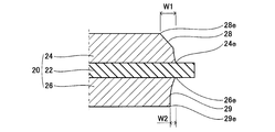
- a thin-walled portion 28 is provided on the first inner conductor layer 24 of the first insulating circuit board 20.
- the thin portion 28 extends along the outer peripheral edge 24e of the first inner conductor layer 24 with a first width W1.
- the width W1 of the thin-walled portion 28 means the distance from the outer peripheral edge 24e of the first inner conductor layer 24 to the inner peripheral edge 28e of the thin-walled portion 28.
- the thickness Da of the first inner conductor layer 24 decreases toward the outside (that is, toward the outer peripheral edge 24e).
- the surface of the first inner conductor layer 24 is an inclined surface that is inclined at a constant inclination angle C1.
- Such a thin portion 28 can be formed by, for example, chamfering.
- the first outer conductor layer 26 is not provided with such a thin-walled portion 28.
- the thickness Da of the first inner conductor layer 24 is larger than the thickness Db of the first outer conductor layer 26, except for the thin portion 28. According to such a configuration, the heat capacity of the first inner conductor layer 24 close to the semiconductor elements 12 and 14 becomes large, and the temperature change of the semiconductor elements 12 and 14 is suppressed.
- the first inner conductor layer 24 of the first insulating circuit board 20 is located inside the sealing body 52.
- the thermal stress generated in the sealing body 52 tends to increase locally in the vicinity of the outer peripheral edge 24e of the first inner conductor layer 24.
- the thin portion 28 is formed on the outer peripheral edge 24e of the first inner conductor layer 24, such concentration of thermal stress can be relaxed.
- the outer peripheral edge 26e of the first outer conductor layer 26 is not provided with a thin-walled portion, the peeling of the sealing body 52 on the outer peripheral edge 26e as described above is suppressed.
- the thin-walled portion 38 is also provided in the second inner conductor layer 34 of the second insulating circuit board 30.
- the thin portion 38 extends along the outer peripheral edge 34e of the second inner conductor layer 34 with a third width W3. That is, the distance from the outer peripheral edge 34e of the second inner conductor layer 34 to the inner peripheral edge 38e of the thin portion 38 is W3.
- the thickness of the second inner conductor layer 34 decreases toward the outside (that is, toward the outer peripheral edge 34e).
- such a thin portion 38 is not provided in the second outer conductor layer 36.
- the concentration of thermal stress is relaxed in the vicinity of the outer peripheral edge 34e of the second inner conductor layer 34, and the second insulating circuit board 30 is also sealed at the outer peripheral edge 36e of the second outer conductor layer 36. The peeling of the body 52 is prevented.
- the sealing body 52 is formed.
- the concentration of generated thermal stress can be suppressed.
- the inner peripheral edge 28e of the thin-walled portion 28 of the first inner conductor layer 24 is the thin-walled portion 38 of the second inner conductor layer 34. It is preferable to be located outside the inner peripheral edge 38e. Further, the inner peripheral edge 28e of the thin portion 28 of the first inner conductor layer 24 may be located outside the outer peripheral edge 34e of the second inner conductor layer 34.
- the concentration of thermal stress generated in the sealing body 52 can be further suppressed.
- the positional relationship of the outer peripheral edges 24e and 34e may be exchanged between the two inner conductor layers 24 and 34.
- the thin portion 28 of the first inner conductor layer 24 can be designed into various shapes.
- the angle Ca at the inner peripheral edge 28e of the thin portion 28 can be larger than 90 degrees and 135 degrees or less.
- the inclination angle C1 in the thin portion 28 is 45 degrees or more and smaller than 90 degrees. If the angle Ca on the inner peripheral edge 28e exceeds 135 degrees, the angle Cb on the outer peripheral edge 24e of the first inner conductor layer 24 becomes smaller, which may increase the thermal stress of the sealing body 52 in the vicinity of the outer peripheral edge 24e. Invite.
- the minimum thickness Da'of the thin-walled portion 28 of the first inner conductor layer 24 can be half or more of the thickness Da'other than the thin-walled portion 28 of the first inner conductor layer 24. These points are the same for the thin portion 38 of the second inner conductor layer 34.
- the first outer conductor layer 26 may also have a thin portion 29.
- the thin portion 29 extends along the outer peripheral edge 26e of the first outer conductor layer 26 with a second width W2 smaller than the first width W1. Also in this thin portion 29, the thickness of the first outer conductor layer 26 decreases toward the outside (that is, toward the outer peripheral edge 26e).
- the thin portion 29 of the first outer conductor layer 26 is not intentionally provided, but is formed by etching for pattern forming the first outer conductor layer 26, and is a curved surface that curves in a concave shape. It has become.
- the second outer conductor layer 36 may also be provided with a thin-walled portion along the outer peripheral edge thereof.
- the width of the thin portion of the second outer conductor layer 36 is preferably smaller than the width of the thin portion of the second inner conductor layer 34 (third width W3).
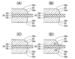
- the thin portion 28 of the first inner conductor layer 24 has a curved surface in which the surface of the first inner conductor layer 24 is curved in a convex shape.
- the thin portion 29 of the first outer conductor layer 26 also has a curved surface in which the surface of the first outer conductor layer 26 is curved in a convex shape.
- the radius of curvature of the thin portion 28 of the first inner conductor layer 24 is larger than the radius of curvature of the thin portion 29 of the first outer conductor layer 26.
- the surface of the first inner conductor layer 24 has two or more inclined surfaces having different inclination angles.
- the surface of the first inner conductor layer 24 has two or more curved surfaces, and a convex curved surface and a concave shape. The curved surfaces of are located alternately. Then, in the modified example shown in FIG. 9D, the inclination angle C1 of the thin-walled portion 28 of the first inner conductor layer 24 is smaller than the inclination angle C2 of the thin-walled portion 29 of the first outer conductor layer 26. In any of the modified examples shown in FIGS.
- the width of the thin-walled portion 29 of the first outer conductor layer 26 is smaller than the width of the thin-walled portion 28 of the first inner conductor layer 24. .. Further, the configuration of the modified example shown in FIGS. 9 (A) to 9 (D) can be similarly adopted for the second insulated circuit board 30.
- the size of the first inner conductor layer 24 may be different from the size of the first outer conductor layer 26.
- the size of the first inner conductor layer 24 may be larger than the size of the first outer conductor layer 26. That is, when the first insulating circuit board 20 is viewed in a plan view, the outer peripheral edge 24e of the first inner conductor layer 24 may be located outside the outer peripheral edge 26e of the first outer conductor layer 26. According to such a configuration, the heat capacity of the first inner conductor layer 24 close to the semiconductor elements 12 and 14 becomes large, and the temperature change of the semiconductor elements 12 and 14 is suppressed.
- the inner peripheral edge 28e of the thin-walled portion 28 of the first inner conductor layer 24 may be located inside the inner peripheral edge 29e of the thin-walled portion 29 of the first outer conductor layer 26. According to such a configuration, the width of the thin portion 28 of the first inner conductor layer 24 (that is, the first width W1) is increased, and the concentration of thermal stress generated in the sealing body 52 is effectively relaxed.
- the semiconductor device 10 includes a plurality of semiconductor elements 12 and 14 and a plurality of insulated circuit boards 20 and 30.
- the techniques disclosed herein are encapsulations that seal at least one insulating circuit board, at least one semiconductor element disposed on the at least one insulating circuit board, and at least one of the semiconductor elements. It can be meaningfully applied to a semiconductor device including a body.
- Second semiconductor element Semiconductor device 12: First semiconductor element 14: Second semiconductor element 20: First insulating circuit board 22: First insulator substrate 24: First inner conductor layer 26: First outer conductor layer 28: First inner conductor Thin-walled portion 29 of the layer: Thin-walled portion of the first outer conductor layer 30: Second insulating circuit board 32: Second insulator substrate 34: Second inner conductor layer 36: Second outer conductor layer 38: Second inner conductor layer Thin wall portion 40: Connecting members 42, 44, 46: Power terminal 48, 50: Signal terminal 52: Insulator
Landscapes
- Cooling Or The Like Of Semiconductors Or Solid State Devices (AREA)
- Engineering & Computer Science (AREA)
- Microelectronics & Electronic Packaging (AREA)
- Road Paving Machines (AREA)
- Structure Of Printed Boards (AREA)
Priority Applications (4)
| Application Number | Priority Date | Filing Date | Title |
|---|---|---|---|
| PCT/JP2019/045298 WO2021100126A1 (ja) | 2019-11-19 | 2019-11-19 | 半導体装置 |
| JP2021558080A JP7103533B2 (ja) | 2019-11-19 | 2019-11-19 | 半導体装置 |
| US17/746,492 US12159810B2 (en) | 2019-11-19 | 2022-05-17 | Semiconductor device |
| US18/928,536 US20250069967A1 (en) | 2019-11-19 | 2024-10-28 | Semiconductor device |
Applications Claiming Priority (1)
| Application Number | Priority Date | Filing Date | Title |
|---|---|---|---|
| PCT/JP2019/045298 WO2021100126A1 (ja) | 2019-11-19 | 2019-11-19 | 半導体装置 |
Related Child Applications (1)
| Application Number | Title | Priority Date | Filing Date |
|---|---|---|---|
| US17/746,492 Continuation US12159810B2 (en) | 2019-11-19 | 2022-05-17 | Semiconductor device |
Publications (1)
| Publication Number | Publication Date |
|---|---|
| WO2021100126A1 true WO2021100126A1 (ja) | 2021-05-27 |
Family
ID=75980408
Family Applications (1)
| Application Number | Title | Priority Date | Filing Date |
|---|---|---|---|
| PCT/JP2019/045298 Ceased WO2021100126A1 (ja) | 2019-11-19 | 2019-11-19 | 半導体装置 |
Country Status (3)
| Country | Link |
|---|---|
| US (2) | US12159810B2 (https=) |
| JP (1) | JP7103533B2 (https=) |
| WO (1) | WO2021100126A1 (https=) |
Families Citing this family (1)
| Publication number | Priority date | Publication date | Assignee | Title |
|---|---|---|---|---|
| DE102023205266A1 (de) | 2023-06-06 | 2024-12-12 | Infineon Technologies Ag | Halbleitermodul, leistungselektronisches Substrat und Verfahren zum Herstellen eines Halbleitermoduls |
Citations (5)
| Publication number | Priority date | Publication date | Assignee | Title |
|---|---|---|---|---|
| JPS6459986A (en) * | 1987-08-31 | 1989-03-07 | Toshiba Corp | Ceramic circuit board |
| JP2002076197A (ja) * | 2000-08-24 | 2002-03-15 | Toshiba Corp | 半導体装置用基板及び半導体装置 |
| JP2003068978A (ja) * | 2001-08-28 | 2003-03-07 | Hitachi Ltd | 半導体装置及びその製造方法 |
| JP2015015434A (ja) * | 2013-07-08 | 2015-01-22 | 三菱電機株式会社 | モジュール構造 |
| JP2016092184A (ja) * | 2014-11-04 | 2016-05-23 | トヨタ自動車株式会社 | パワーモジュール |
Family Cites Families (5)
| Publication number | Priority date | Publication date | Assignee | Title |
|---|---|---|---|---|
| JP6394489B2 (ja) * | 2015-05-11 | 2018-09-26 | 株式会社デンソー | 半導体装置 |
| JP2019067949A (ja) * | 2017-10-02 | 2019-04-25 | トヨタ自動車株式会社 | 半導体装置 |
| JP2019083294A (ja) * | 2017-10-31 | 2019-05-30 | トヨタ自動車株式会社 | 半導体装置とその製造方法 |
| JP7095632B2 (ja) * | 2019-03-11 | 2022-07-05 | 株式会社デンソー | 半導体装置 |
| US11646249B2 (en) * | 2020-12-29 | 2023-05-09 | Semiconductor Components Industries, Llc | Dual-side cooling semiconductor packages and related methods |
-
2019
- 2019-11-19 WO PCT/JP2019/045298 patent/WO2021100126A1/ja not_active Ceased
- 2019-11-19 JP JP2021558080A patent/JP7103533B2/ja active Active
-
2022
- 2022-05-17 US US17/746,492 patent/US12159810B2/en active Active
-
2024
- 2024-10-28 US US18/928,536 patent/US20250069967A1/en active Pending
Patent Citations (5)
| Publication number | Priority date | Publication date | Assignee | Title |
|---|---|---|---|---|
| JPS6459986A (en) * | 1987-08-31 | 1989-03-07 | Toshiba Corp | Ceramic circuit board |
| JP2002076197A (ja) * | 2000-08-24 | 2002-03-15 | Toshiba Corp | 半導体装置用基板及び半導体装置 |
| JP2003068978A (ja) * | 2001-08-28 | 2003-03-07 | Hitachi Ltd | 半導体装置及びその製造方法 |
| JP2015015434A (ja) * | 2013-07-08 | 2015-01-22 | 三菱電機株式会社 | モジュール構造 |
| JP2016092184A (ja) * | 2014-11-04 | 2016-05-23 | トヨタ自動車株式会社 | パワーモジュール |
Also Published As
| Publication number | Publication date |
|---|---|
| JP7103533B2 (ja) | 2022-07-20 |
| US20220278006A1 (en) | 2022-09-01 |
| US12159810B2 (en) | 2024-12-03 |
| US20250069967A1 (en) | 2025-02-27 |
| JPWO2021100126A1 (https=) | 2021-05-27 |
Similar Documents
| Publication | Publication Date | Title |
|---|---|---|
| US12125823B2 (en) | Semiconductor device including inner conductive layer having regions of different surface roughness | |
| JP7155748B2 (ja) | 半導体装置 | |
| JP7069787B2 (ja) | 半導体装置 | |
| CN110600457B (zh) | 半导体装置 | |
| JP2019145776A (ja) | 半導体装置 | |
| US11201099B2 (en) | Semiconductor device and method of manufacturing the same | |
| JP7163583B2 (ja) | 半導体装置 | |
| US20250069967A1 (en) | Semiconductor device | |
| CN110943062B (zh) | 半导体装置 | |
| JP2004040900A (ja) | 半導体モジュール及び電力変換装置 | |
| US20220392819A1 (en) | Semiconductor device and method of manufacturing the same | |
| US11749620B2 (en) | Semiconductor module | |
| JP7192886B2 (ja) | 半導体装置 | |
| WO2021095146A1 (ja) | 半導体装置 | |
| JP7159609B2 (ja) | 半導体装置 | |
| CN121123122A (zh) | 半导体装置 | |
| JP2021093499A (ja) | 半導体装置 | |
| JP2021111719A (ja) | 半導体装置 | |
| WO2020179143A1 (ja) | 半導体装置 | |
| JP2020188172A (ja) | 半導体装置 | |
| JP2020188106A (ja) | 半導体モジュール | |
| JP2020188105A (ja) | 半導体モジュール |
Legal Events
| Date | Code | Title | Description |
|---|---|---|---|
| 121 | Ep: the epo has been informed by wipo that ep was designated in this application |
Ref document number: 19953410 Country of ref document: EP Kind code of ref document: A1 |
|
| ENP | Entry into the national phase |
Ref document number: 2021558080 Country of ref document: JP Kind code of ref document: A |
|
| NENP | Non-entry into the national phase |
Ref country code: DE |
|
| 122 | Ep: pct application non-entry in european phase |
Ref document number: 19953410 Country of ref document: EP Kind code of ref document: A1 |