WO2021090603A1 - センサユニット - Google Patents
センサユニット Download PDFInfo
- Publication number
- WO2021090603A1 WO2021090603A1 PCT/JP2020/036369 JP2020036369W WO2021090603A1 WO 2021090603 A1 WO2021090603 A1 WO 2021090603A1 JP 2020036369 W JP2020036369 W JP 2020036369W WO 2021090603 A1 WO2021090603 A1 WO 2021090603A1
- Authority
- WO
- WIPO (PCT)
- Prior art keywords
- bus bar
- predetermined direction
- sensor unit
- resin
- bus bars
- Prior art date
- Legal status (The legal status is an assumption and is not a legal conclusion. Google has not performed a legal analysis and makes no representation as to the accuracy of the status listed.)
- Ceased
Links
Images


Classifications
-
- G—PHYSICS
- G01—MEASURING; TESTING
- G01R—MEASURING ELECTRIC VARIABLES; MEASURING MAGNETIC VARIABLES
- G01R15/00—Details of measuring arrangements of the types provided for in groups G01R17/00 - G01R29/00, G01R33/00 - G01R33/26 or G01R35/00
- G01R15/14—Adaptations providing voltage or current isolation, e.g. for high-voltage or high-current networks
- G01R15/20—Adaptations providing voltage or current isolation, e.g. for high-voltage or high-current networks using galvano-magnetic devices, e.g. Hall-effect devices, i.e. measuring a magnetic field via the interaction between a current and a magnetic field, e.g. magneto resistive or Hall effect devices
- G01R15/205—Adaptations providing voltage or current isolation, e.g. for high-voltage or high-current networks using galvano-magnetic devices, e.g. Hall-effect devices, i.e. measuring a magnetic field via the interaction between a current and a magnetic field, e.g. magneto resistive or Hall effect devices using magneto-resistance devices, e.g. field plates
-
- H—ELECTRICITY
- H02—GENERATION; CONVERSION OR DISTRIBUTION OF ELECTRIC POWER
- H02M—APPARATUS FOR CONVERSION BETWEEN AC AND AC, BETWEEN AC AND DC, OR BETWEEN DC AND DC, AND FOR USE WITH MAINS OR SIMILAR POWER SUPPLY SYSTEMS; CONVERSION OF DC OR AC INPUT POWER INTO SURGE OUTPUT POWER; CONTROL OR REGULATION THEREOF
- H02M7/00—Conversion of AC power input into DC power output; Conversion of DC power input into AC power output
- H02M7/003—Constructional details, e.g. physical layout, assembly, wiring or busbar connections
-
- G—PHYSICS
- G01—MEASURING; TESTING
- G01R—MEASURING ELECTRIC VARIABLES; MEASURING MAGNETIC VARIABLES
- G01R15/00—Details of measuring arrangements of the types provided for in groups G01R17/00 - G01R29/00, G01R33/00 - G01R33/26 or G01R35/00
- G01R15/14—Adaptations providing voltage or current isolation, e.g. for high-voltage or high-current networks
- G01R15/20—Adaptations providing voltage or current isolation, e.g. for high-voltage or high-current networks using galvano-magnetic devices, e.g. Hall-effect devices, i.e. measuring a magnetic field via the interaction between a current and a magnetic field, e.g. magneto resistive or Hall effect devices
-
- H—ELECTRICITY
- H02—GENERATION; CONVERSION OR DISTRIBUTION OF ELECTRIC POWER
- H02M—APPARATUS FOR CONVERSION BETWEEN AC AND AC, BETWEEN AC AND DC, OR BETWEEN DC AND DC, AND FOR USE WITH MAINS OR SIMILAR POWER SUPPLY SYSTEMS; CONVERSION OF DC OR AC INPUT POWER INTO SURGE OUTPUT POWER; CONTROL OR REGULATION THEREOF
- H02M1/00—Details of apparatus for conversion
- H02M1/0003—Details of control, feedback or regulation circuits
- H02M1/0009—Devices or circuits for detecting current in a converter
-
- H—ELECTRICITY
- H02—GENERATION; CONVERSION OR DISTRIBUTION OF ELECTRIC POWER
- H02M—APPARATUS FOR CONVERSION BETWEEN AC AND AC, BETWEEN AC AND DC, OR BETWEEN DC AND DC, AND FOR USE WITH MAINS OR SIMILAR POWER SUPPLY SYSTEMS; CONVERSION OF DC OR AC INPUT POWER INTO SURGE OUTPUT POWER; CONTROL OR REGULATION THEREOF
- H02M3/00—Conversion of DC power input into DC power output
- H02M3/003—Constructional details, e.g. physical layout, assembly, wiring or busbar connections
-
- H—ELECTRICITY
- H02—GENERATION; CONVERSION OR DISTRIBUTION OF ELECTRIC POWER
- H02M—APPARATUS FOR CONVERSION BETWEEN AC AND AC, BETWEEN AC AND DC, OR BETWEEN DC AND DC, AND FOR USE WITH MAINS OR SIMILAR POWER SUPPLY SYSTEMS; CONVERSION OF DC OR AC INPUT POWER INTO SURGE OUTPUT POWER; CONTROL OR REGULATION THEREOF
- H02M1/00—Details of apparatus for conversion
- H02M1/0067—Converter structures employing plural converter units, other than for parallel operation of the units on a single load
- H02M1/007—Plural converter units in cascade
-
- H—ELECTRICITY
- H02—GENERATION; CONVERSION OR DISTRIBUTION OF ELECTRIC POWER
- H02M—APPARATUS FOR CONVERSION BETWEEN AC AND AC, BETWEEN AC AND DC, OR BETWEEN DC AND DC, AND FOR USE WITH MAINS OR SIMILAR POWER SUPPLY SYSTEMS; CONVERSION OF DC OR AC INPUT POWER INTO SURGE OUTPUT POWER; CONTROL OR REGULATION THEREOF
- H02M1/00—Details of apparatus for conversion
- H02M1/0067—Converter structures employing plural converter units, other than for parallel operation of the units on a single load
- H02M1/008—Plural converter units for generating at two or more independent and non-parallel outputs, e.g. systems with plural point of load switching regulators
-
- H—ELECTRICITY
- H02—GENERATION; CONVERSION OR DISTRIBUTION OF ELECTRIC POWER
- H02M—APPARATUS FOR CONVERSION BETWEEN AC AND AC, BETWEEN AC AND DC, OR BETWEEN DC AND DC, AND FOR USE WITH MAINS OR SIMILAR POWER SUPPLY SYSTEMS; CONVERSION OF DC OR AC INPUT POWER INTO SURGE OUTPUT POWER; CONTROL OR REGULATION THEREOF
- H02M3/00—Conversion of DC power input into DC power output
- H02M3/02—Conversion of DC power input into DC power output without intermediate conversion into AC
- H02M3/04—Conversion of DC power input into DC power output without intermediate conversion into AC by static converters
- H02M3/10—Conversion of DC power input into DC power output without intermediate conversion into AC by static converters using discharge tubes with control electrode or semiconductor devices with control electrode
- H02M3/145—Conversion of DC power input into DC power output without intermediate conversion into AC by static converters using discharge tubes with control electrode or semiconductor devices with control electrode using devices of a triode or transistor type requiring continuous application of a control signal
- H02M3/155—Conversion of DC power input into DC power output without intermediate conversion into AC by static converters using discharge tubes with control electrode or semiconductor devices with control electrode using devices of a triode or transistor type requiring continuous application of a control signal using semiconductor devices only
- H02M3/156—Conversion of DC power input into DC power output without intermediate conversion into AC by static converters using discharge tubes with control electrode or semiconductor devices with control electrode using devices of a triode or transistor type requiring continuous application of a control signal using semiconductor devices only with automatic control of output voltage or current, e.g. switching regulators
- H02M3/158—Conversion of DC power input into DC power output without intermediate conversion into AC by static converters using discharge tubes with control electrode or semiconductor devices with control electrode using devices of a triode or transistor type requiring continuous application of a control signal using semiconductor devices only with automatic control of output voltage or current, e.g. switching regulators including plural semiconductor devices as final control devices for a single load
-
- H—ELECTRICITY
- H02—GENERATION; CONVERSION OR DISTRIBUTION OF ELECTRIC POWER
- H02M—APPARATUS FOR CONVERSION BETWEEN AC AND AC, BETWEEN AC AND DC, OR BETWEEN DC AND DC, AND FOR USE WITH MAINS OR SIMILAR POWER SUPPLY SYSTEMS; CONVERSION OF DC OR AC INPUT POWER INTO SURGE OUTPUT POWER; CONTROL OR REGULATION THEREOF
- H02M7/00—Conversion of AC power input into DC power output; Conversion of DC power input into AC power output
- H02M7/42—Conversion of DC power input into AC power output without possibility of reversal
- H02M7/44—Conversion of DC power input into AC power output without possibility of reversal by static converters
- H02M7/48—Conversion of DC power input into AC power output without possibility of reversal by static converters using discharge tubes with control electrode or semiconductor devices with control electrode
- H02M7/53—Conversion of DC power input into AC power output without possibility of reversal by static converters using discharge tubes with control electrode or semiconductor devices with control electrode using devices of a triode or transistor type requiring continuous application of a control signal
- H02M7/537—Conversion of DC power input into AC power output without possibility of reversal by static converters using discharge tubes with control electrode or semiconductor devices with control electrode using devices of a triode or transistor type requiring continuous application of a control signal using semiconductor devices only, e.g. single switched pulse inverters
- H02M7/5387—Conversion of DC power input into AC power output without possibility of reversal by static converters using discharge tubes with control electrode or semiconductor devices with control electrode using devices of a triode or transistor type requiring continuous application of a control signal using semiconductor devices only, e.g. single switched pulse inverters in a bridge configuration
Definitions
- the disclosure described in this specification relates to a sensor unit including a bus bar connected to a switch module and a magnetron conversion unit for detecting a current flowing through the bus bar.
- an inverter device including a plurality of bus bars integrally molded on an insulating member and a plurality of current sensors provided on the insulating member in a manner facing each of the plurality of bus bars is known. There is.
- An object of the present disclosure is to provide a sensor unit in which a decrease in current detection accuracy is suppressed.
- the sensor unit includes a plurality of bus bars arranged separately in a first predetermined direction, which are individually connected to each of a plurality of switch modules constituting a part of the power conversion circuit.
- An insulating resin case extending in a first predetermined direction, which connects a part of each of the plurality of bus bars in a buried manner, A magnetic field generated by the flow of current flowing through a plurality of bus bars is detected by being provided in the resin case so as to face each of the buried parts embedded in the resin case in each of the plurality of bus bars in a second predetermined direction intersecting the first predetermined direction.
- the resin case is prevented from warping due to thermal expansion and contraction. It is possible to prevent a change in the relative positional relationship between the plurality of magnetron conversion units provided in the resin case and the plurality of bus bars connected to the resin case. As a result, fluctuations in the magnetic field transmitted through the magnetron conversion unit are suppressed. The decrease in current detection accuracy of the magnetron conversion unit is suppressed.
- the in-vehicle system 100 constitutes a hybrid system.
- the in-vehicle system 100 includes a battery 200, a power conversion device 300, and a motor 400.
- the in-vehicle system 100 also includes an engine 500 and a power distribution mechanism 600.
- the power converter 300 includes a sensor unit 700.
- the motor 400 has a first MG 401 and a second MG 402. MG is an abbreviation for motor generator.
- the in-vehicle system 100 has a plurality of ECUs (not shown). These plurality of ECUs send and receive signals to and from each other via bus wiring. The plurality of ECUs cooperate to control the hybrid vehicle. By the coordinated control of the plurality of ECUs, the power running and power generation (regeneration) of the motor 400 according to the SOC of the battery 200, the output of the engine 500, and the like are controlled. SOC is an abbreviation for state of charge. ECU is an abbreviation for electronic control unit.
- the ECU has at least one arithmetic processing unit (CPU) and at least one memory device (MMR) as a storage medium for storing programs and data.
- the ECU is provided by a microcomputer or a microprocessor having a storage medium that can be read by a processor.
- a storage medium is a non-transitional substantive storage medium that non-temporarily stores a program that can be read by a computer or processor.
- the storage medium may be provided by a semiconductor memory, a magnetic disk, or the like.
- Battery 200 has a plurality of secondary batteries. These plurality of secondary batteries form a battery stack connected in series.
- a lithium ion secondary battery, a nickel hydrogen secondary battery, an organic radical battery, or the like can be adopted.
- the secondary battery generates an electromotive voltage by a chemical reaction.
- the secondary battery has the property of accelerating deterioration when the amount of charge is too high or too low. In other words, the secondary battery has a property that deterioration is accelerated when the SOC is overcharged or overdischarged.
- the SOC of the battery 200 corresponds to the SOC of the above battery stack.
- the SOC of the battery stack is the sum of the SOCs of a plurality of secondary batteries. Overcharging and overdischarging of the SOC of the battery stack is avoided by the above-mentioned cooperative control. On the other hand, overcharging and overdischarging of the SOCs of the plurality of secondary batteries are avoided by the equalization process for equalizing the SOCs of the plurality of secondary batteries.
- the equalization process is performed by charging and discharging a plurality of secondary batteries individually.
- the battery 200 is provided with a monitoring unit including a switch for individually charging and discharging a plurality of secondary batteries. Further, the battery 200 is provided with a voltage sensor, a temperature sensor, and the like for detecting the SOC of each of the plurality of secondary batteries.
- One of the plurality of ECUs, the battery ECU controls the opening and closing of the switch based on the output of these sensors and the like. As a result, the SOC of each of the plurality of secondary batteries is equalized.
- the output of the current sensor 730 which will be described later, is also used for SOC detection.
- the power conversion device 300 performs power conversion between the battery 200 and the first MG 401.
- the power conversion device 300 also performs power conversion between the battery 200 and the second MG 402.
- the power conversion device 300 converts the DC power of the battery 200 into AC power having a voltage level suitable for the power running of the first MG 401 and the second MG 402.
- the power conversion device 300 converts the AC power generated by the power generation of the first MG 401 and the second MG 402 into DC power having a voltage level suitable for charging the battery 200.
- the power converter 300 will be described in detail later.
- the first MG401, the second MG402, and the engine 500 are each connected to the power distribution mechanism 600.
- the first MG 401 generates electricity by the rotational energy supplied from the engine 500.
- the AC power generated by this power generation is converted into DC power by the power conversion device 300 and is stepped down. This DC power is supplied to the battery 200.
- DC power is also supplied to various electric loads mounted on hybrid vehicles.
- the second MG402 is connected to the output shaft of the hybrid vehicle.
- the rotational energy of the second MG 402 is transmitted to the traveling wheels via the output shaft.
- the rotational energy of the traveling wheel is transmitted to the second MG 402 via the output shaft.
- the second MG 402 is powered by the AC power supplied from the power converter 300.
- the rotational energy generated by this power running is distributed to the engine 500 and the traveling wheels by the power distribution mechanism 600.
- crankshaft cranking and propulsive force are given to the traveling wheels.
- the second MG 402 is regenerated by the rotational energy transmitted from the traveling wheels.
- the AC power generated by this regeneration is converted into DC power by the power conversion device 300 and is stepped down. This DC power is supplied to the battery 200 and various electric loads.
- the rated current of the 2nd MG402 is larger than that of the 1st MG401. A larger amount of current is more likely to flow in the second MG 402 than in the first MG 401.
- the engine 500 generates rotational energy by driving fuel by combustion. This rotational energy is distributed to the first MG 401 and the second MG 402 via the power distribution mechanism 600. As a result, the power generation of the first MG401 and the propulsive force are given to the traveling wheels.
- the power distribution mechanism 600 has a planetary gear mechanism.
- the power distribution mechanism 600 includes a sun gear, a planetary gear, a planetary carrier, and a ring gear.
- the sun gear and planetary gear each form a disk shape.
- a plurality of teeth are formed side by side in the circumferential direction on the circumferential surface of each of the sun gear and the planetary gear.
- the planetary carrier forms a ring.
- a plurality of planetary gears are connected to the flat surfaces of the planetary carrier in such a manner that the flat surfaces of the planetary carrier and the planetary gears face each other.
- Multiple planetary gears are located on the circumference centered on the center of rotation of the planetary carrier. The adjacent spacing of these plurality of planetary gears is equal. In this embodiment, three planetary gears are arranged at 120 ° intervals.
- the ring gear forms a ring.
- a plurality of teeth are formed side by side in the circumferential direction on each of the outer peripheral surface and the inner peripheral surface of the ring gear.
- the sun gear is provided in the center of the ring gear.
- the outer peripheral surface of the sun gear and the inner peripheral surface of the ring gear face each other.
- Three planetary gears are provided between the two.
- the teeth of each of the three planetary gears mesh with the teeth of the sun gear and ring gear.
- the motor shaft of the 1st MG401 is connected to the sun gear.
- the crankshaft of the engine 500 is connected to the planetary carrier.
- the motor shaft of the second MG 402 is connected to the ring gear.
- Torque is generated in the sun gear and ring gear by supplying AC power from the power converter 300 to the first MG 401 and the second MG 402. Torque is generated in the planetary carrier by the combustion drive of the engine 500. As a result, power generation of the first MG 401, power running and regeneration of the second MG 402, and application of propulsive force to the traveling wheels are performed.
- one of the above-mentioned plurality of ECUs has the first MG 401 and the second MG 402 based on the physical quantities detected by various sensors mounted on the hybrid vehicle, the vehicle information input from the other ECUs, and the like. Determine each target torque. Then, the MG ECU vector-controls the torque generated in each of the first MG 401 and the second MG 402 so as to be the target torque.
- This MGECU is mounted on a control circuit board described later.
- the power conversion device 300 includes a converter 310 and an inverter 320 as components of the power conversion circuit.
- the converter 310 functions to raise or lower the voltage level of DC power.
- the inverter 320 functions to convert DC power into AC power.
- the inverter 320 functions to convert AC power into DC power.
- the converter 310 boosts the DC power of the battery 200 to a voltage level suitable for torque generation of the first MG 401 and the second MG 402.
- the inverter 320 converts this DC power into AC power. This AC power is supplied to the first MG401 and the second MG402. Further, the inverter 320 converts the AC power generated by the first MG 401 and the second MG 402 into DC power.
- the converter 310 steps down this DC power to a voltage level suitable for charging the battery 200.
- the converter 310 is electrically connected to the battery 200 via the positive electrode bus bar 301 and the negative electrode bus bar 302.
- the converter 310 is electrically connected to the inverter 320 via the P bus bar 303 and the N bus bar 304.
- the converter 310 has a filter capacitor 311 as an electric element, an A-phase switch module 312, and an A-phase reactor 313.
- one end of the positive electrode bus bar 301 is connected to the positive electrode of the battery 200.
- One end of the negative electrode bus bar 302 is connected to the negative electrode of the battery 200.
- One of the two electrodes of the filter capacitor 311 is connected to the positive electrode bus bar 301.
- the other of the two electrodes of the filter capacitor 311 is connected to the negative electrode bus bar 302.
- One end of the A-phase reactor 313 is connected to the other end of the positive electrode bus bar 301.
- the other end of the A-phase reactor 313 is connected to the A-phase switch module 312 via the first connecting bus bar 711.
- the positive electrode of the battery 200 and the A-phase switch module 312 are electrically connected via the A-phase reactor 313 and the first connecting bus bar 711.
- the connection parts of various bus bars are indicated by white circles. These connection parts are electrically connected by, for example, bolts or welding.
- the A-phase switch module 312 has a high-side switch 331 and a low-side switch 332. Further, the A-phase switch module 312 has a high-side diode 331a and a low-side diode 332a. These semiconductor elements are coated and protected by a sealing resin (not shown).
- an n-channel type IGBT is adopted as the high side switch 331 and the low side switch 332.
- the collector electrodes, emitter electrodes, and terminals connected to the gate electrodes of the high-side switch 331 and the low-side switch 332 are exposed to the outside of the sealing resin.
- the emitter electrode of the high side switch 331 and the collector electrode of the low side switch 332 are connected.
- the high side switch 331 and the low side switch 332 are connected in series.
- the cathode electrode of the high side diode 331a is connected to the collector electrode of the high side switch 331.
- the anode electrode of the high side diode 331a is connected to the emitter electrode of the high side switch 331.
- the high-side diode 331a is connected in antiparallel to the high-side switch 331.
- the cathode electrode of the low side diode 332a is connected to the collector electrode of the low side switch 332.
- the anode electrode of the low side diode 332a is connected to the emitter electrode of the low side switch 332.
- the low-side diode 332a is connected in anti-parallel to the low-side switch 332.
- the high side switch 331 and the low side switch 332 are covered and protected by the sealing resin. From this sealing resin, the collector electrode and gate electrode of the high side switch 331, the midpoint between the high side switch 331 and the low side switch 332, and the tip of the terminal connected to the emitter electrode and the gate electrode of the low side switch 332, respectively. It is exposed.
- these terminals are referred to as a collector terminal 330a, a midpoint terminal 330c, an emitter terminal 330b, and a gate terminal 330d.
- This collector terminal 330a is connected to the P bus bar 303.
- the emitter terminal 330b is connected to the N bus bar 304.
- the midpoint terminal 330c is connected to the first connection bus bar 711.
- the first connected bus bar 711 is electrically connected to the positive electrode of the battery 200 via the phase A reactor 313 and the positive electrode bus bar 301.
- the DC power of the battery 200 is supplied to the midpoint of the two switches included in the A-phase switch module 312 via the positive electrode bus bar 301, the A-phase reactor 313, and the first connected bus bar 711.
- the AC power of the motor 400 converted into DC power by the inverter 320 is supplied to the collector electrode of the high side switch 331 of the A-phase switch module 312.
- the AC power of the motor 400 converted into the DC power is supplied to the battery 200 via the high side switch 331, the first connected bus bar 711, the A-phase reactor 313, and the positive electrode bus bar 301.
- the gate terminals 330d of each of the high side switch 331 and the low side switch 332 are connected to the above gate driver.
- the MGECU generates a control signal and outputs it to the gate driver.
- the gate driver amplifies the control signal and outputs it to the gate terminal 330d.
- the high-side switch 331 and the low-side switch 332 are controlled to open and close by the MGECU.
- the voltage level of the DC power input to the converter 310 is stepped up and down.
- the MGECU generates a pulse signal as a control signal.
- the MGECU adjusts the buck-boost level of DC power by adjusting the on-duty ratio and frequency of this pulse signal. This buck-boost level is determined according to the target torque of the motor 400 and the SOC of the battery 200.
- the MGECU When boosting the DC power of the battery 200, the MGECU alternately opens and closes the high-side switch 331 and the low-side switch 332. On the contrary, when the DC power supplied from the inverter 320 is stepped down, the MGECU fixes the control signal output to the low side switch 332 to a low level. At the same time, the MGECU sequentially switches the control signal output to the high side switch 331 between the high level and the low level.
- the inverter 320 has a smoothing capacitor 321 as an electric element, a discharge resistor (not shown), and a U-phase switch module 322 to a Z-phase switch module 327.
- One of the two electrodes of the smoothing capacitor 321 is connected to the P bus bar 303.
- the other of the two electrodes of the smoothing capacitor 321 is connected to the N bus bar 304.
- the discharge resistor is also connected to the P bus bar 303 and the N bus bar 304.
- the U-phase switch modules 322 to Z-phase switch modules 327 are also connected to the P bus bar 303 and the N bus bar 304.
- the smoothing capacitor 321 and the discharge resistor, and the U-phase switch module 322 to the Z-phase switch module 327 are connected in parallel between the P bus bar 303 and the N bus bar 304, respectively.
- Each of the U-phase switch module 322 to the Z-phase switch module 327 has the same components as the A-phase switch module 312. That is, each of the U-phase switch module 322 to the Z-phase switch module 327 has a high-side switch 331, a low-side switch 332, a high-side diode 331a, a low-side diode 332a, and a sealing resin. Each of these 6-phase switch modules has a collector terminal 330a, an emitter terminal 330b, a midpoint terminal 330c, and a gate terminal 330d.
- the collector terminals 330a of each of these 6-phase switch modules are connected to the P bus bar 303.
- the emitter terminal 330b is connected to the N bus bar 304.
- the midpoint terminal 330c of the U-phase switch module 322 is connected to the U-phase stator coil of the first MG401 via the second connecting bus bar 712.
- the midpoint terminal 330c of the V-phase switch module 323 is connected to the V-phase stator coil of the first MG401 via the third connecting bus bar 713.
- the midpoint terminal 330c of the W-phase switch module 324 is connected to the W-phase stator coil of the first MG401 via the fourth connecting bus bar 714.
- the midpoint terminal 330c of the X-phase switch module 325 is connected to the X-phase stator coil of the second MG 402 via the fifth connecting bus bar 715.
- the midpoint terminal 330c of the Y-phase switch module 326 is connected to the Y-phase stator coil of the second MG 402 via the sixth connecting bus bar 716.
- the midpoint terminal 330c of the Z-phase switch module 327 is connected to the Z-phase stator coil of the second MG 402 via the seventh connecting bus bar 717.
- the gate terminal 330d of each of these 6-phase switch modules is connected to the above gate driver.
- the high-side switch 331 and the low-side switch 332 of the six-phase switch module are PWM-controlled by the output of the control signal from the MG ECU.
- a three-phase alternating current is generated in the inverter 320.
- the MG ECU stops the output of the control signal, for example.
- the AC power generated by the power generation passes through the diode provided in the 6-phase switch module.
- AC power is converted to DC power.
- the AC power input / output to and from each of the first MG401 and the second MG402 shown above flows through the second connected bus bar 712 to the seventh connected bus bar 717 that connect each of the first MG 401 and the second MG 402 to the inverter 320.
- the AC power that inputs and outputs each of the first MG401 and the second MG402 flows through the second connected bus bar 712 to the seventh connected bus bar 717.
- the type of switch element provided in each of the A-phase switch module 312 and the U-phase switch module 322 to Z-phase switch module 327 is not particularly limited, and for example, MOSFET can be adopted.
- the semiconductor elements such as switches and diodes included in these switch modules can be manufactured by semiconductors such as Si and wide-gap semiconductors such as SiC.
- the constituent material of the semiconductor element is not particularly limited.
- the x direction corresponds to the first predetermined direction.
- the y direction corresponds to the third predetermined direction.
- the z direction corresponds to the second predetermined direction.
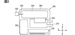
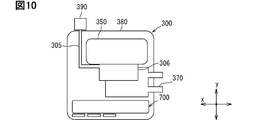
- the power conversion device 300 includes a capacitor case 350, a reactor case 360, a cooler 370, a sensor unit 700, an inverter housing 380, and an input / output connector 390 shown in FIG. Has.
- the positive electrode bus bar 301 and the negative electrode bus bar 302 are collectively shown as the electrode bus bar 305.
- the ends of these two bus bars are provided on the input / output connector 390.
- the terminal of the wire harness is connected to the input / output connector 390.
- the battery 200 and the power conversion device 300 are electrically connected via the wire harness.
- the P bus bar 303 and the N bus bar 304 are collectively shown as a PN bus bar 306. These two bus bars are laminated and arranged in the z direction via an insulating sheet.
- the capacitor case 350 and the reactor case 360 are each made of an insulating resin material.
- a filter capacitor 311 and a smoothing capacitor 321 are housed in the capacitor case 350.
- the A-phase reactor 313 is housed in the reactor case 360.
- the cooler 370 houses the switch module included in the converter 310 and the inverter 320.
- the cooler 370 functions to cool these plurality of switch modules.
- a power module is configured by accommodating a plurality of switch modules in the cooler 370.
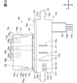
- the sensor unit 700 has a terminal block 720 made of an insulating resin material. A part of the first connecting bus bar 711 to the seventh connecting bus bar 717 described above is insert-molded on the terminal block 720.
- the terminal block 720 is provided with a current sensor 730 that detects the current flowing through the plurality of connected bus bars. The sensor unit 700 will be described in detail later.
- the inverter housing 380 houses the condenser case 350, the reactor case 360, the cooler 370, the sensor unit 700, and the input / output connector 390, respectively.
- the inverter housing 380 also houses the electrode bus bar 305 and the PN bus bar 306.
- the inverter housing 380 is connected to a motor housing that houses the first MG401 and the second MG402, respectively.
- a so-called mechanical / electrical integrated power conversion unit is configured.
- the inverter housing 380 and the motor housing are connected so as to line up in the z direction.
- a part of the PN bus bar 306 is arranged so as to face the cooler 370 in which a plurality of switch modules are housed in the z direction.
- the cooler 370 contains a total of seven switch modules included in the converter 310 and the inverter 320. These switch modules have a sealing resin, and the tips of the collector terminal 330a, the emitter terminal 330b, the midpoint terminal 330c, and the gate terminal 330d are exposed from the sealing resin. Of these four terminals, the collector terminal 330a, the emitter terminal 330b, and the midpoint terminal 330c each extend in the z direction toward the PN bus bar 306. The gate terminal 330d extends in the z direction in the opposite direction to these three terminals.
- the collector terminal 330a is welded to the P bus bar 303.
- the emitter terminal 330b is welded to the N bus bar 304.
- the midpoint terminal 330c is welded to the connecting bus bar included in the sensor unit 700.
- the inverter housing 380 houses a driver board provided with the above gate driver and a control circuit board on which the MGECU is mounted. Each of these driver boards and control circuit boards is lined up with the PN bus bar 306 in the z direction via the cooler 370. The gate terminal 330d is soldered to this driver board. An output pin 723a, which will be described later, is soldered to the control circuit board. The driver board and the control circuit board are electrically connected via wires.
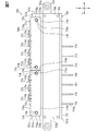
- the sensor unit 700 includes the first connected bus bar 711 to the seventh connected bus bar 717, the terminal block 720, and the current sensor 730 described above. Further, the sensor unit 700 has a shielding shield 740, a resin cover 750, and an opposing shield 760 shown in FIG. Further, the sensor unit 700 has a nut box 770 shown in FIGS. 7 to 9. The nut box 770 corresponds to the support.
- the current sensor 730 has a magnetic equilibrium type first magnetron conversion unit 731 to seventh magnetron conversion unit 737, and a sensor substrate 738 on which these seven magnetron conversion units are mounted.
- the shielding shield 740 has first shielding shields 741 to seventh shielding shields 747 made of a metal material having a higher magnetic permeability than the terminal block 720.
- the facing shield 760 has first facing shield 761 to seventh facing shield 767 made of a metal material having a higher magnetic permeability than the resin cover 750.
- Each of the first connected bus bar 711 to the seventh connected bus bar 717 is insert-molded on the terminal block 720.
- the first magnetron conversion unit 731 to the seventh magnetron conversion unit 737 are provided on the terminal block 720 in a manner facing the portion inserted into the terminal block 720 in these seven connected bus bars in the z direction.
- the first shield shield 741 to the seventh shield shield 747 are insert-molded on the terminal block 720.
- the first facing shield 761 to the seventh facing shield 767 are insert-molded on the resin cover 750.
- the resin cover 750 is provided on the terminal block 720 in such a manner that the seven shielding shields and the seven opposing shields are arranged so as to be separated from each other in the z direction.
- a portion formed into a terminal block 720 in one connecting bus bar and one magnetron conversion unit are located.
- the distribution of the magnetic field (magnetic field to be measured) generated from the current flowing through the portion formed in the terminal block 720 in the connected bus bar is regulated. Fluctuations in the direction of the magnetic field to be measured that passes through the magnetron conversion unit are suppressed.
- the nut box 770 has a first resin body 771 and a second resin body 772, and seven nuts 773 partially embedded therein.
- the first resin body 771 and the second resin body 772 are connected to the terminal block 720.
- the seven nuts 773 function to bolt the first connected bus bar 711 to the seventh connected bus bar 717 to the inner bus bar and the outer bus bar, which will be described later, respectively.
- the components of the sensor unit 700 will be described individually.
- the first connected bus bar 711 to the seventh connected bus bar 717 are made of a metal material such as copper or aluminum, which has a higher rigidity than the terminal block 720. These seven connected bus bars are manufactured by pressing a flat metal plate. The central portion of the seven connecting bus bars is insert-molded into the terminal block 720. Both ends of the seven connecting bus bars are exposed from the terminal block 720.
- the midpoint terminal 330c of the switch module is joined to one end 710a of the first connection bus bar 711 to the seventh connection bus bar 717 exposed from the terminal block 720.
- Seven nuts 773 are individually arranged to face each other at the other end 710b of the first connecting bus bar 711 to the seventh connecting bus bar 717.
- the inner bus bar is bolted to the other end 710b of the first connecting bus bar 711 and one nut 773.
- the inner bus bar is connected to the A-phase reactor 313.
- Six outer bus bars are individually bolted to the other end 710b of the second connecting bus bar 712 to the seventh connecting bus bar 717 and the six nuts 773.
- the outer bus bar is connected to the stator coil of the motor 400 via a wire harness.
- the other end 710b corresponds to the exposed portion.
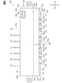
- the terminal block 720 has a base portion 721, a flange portion 722, and a connector portion 723, to be described in detail.
- the base portion 721, the flange portion 722, and the connector portion 723 are integrally connected by the resin material constituting the terminal block 720.
- the base 721 corresponds to the resin case.
- the base 721 has a substantially rectangular parallelepiped shape with the x direction as the longitudinal direction. Therefore, the base portion 721 has a left surface 721a and a right surface 721b arranged in the x direction, a front surface 721c and a rear surface 721d arranged in the y direction, and an upper surface 721e and a lower surface 721f arranged in the z direction.
- the flange portion 722 is integrally connected to each of the left surface 721a and the right surface 721b of the base portion 721.
- One of these two flange portions 722 projects in the x direction so as to be separated from the left surface 721a.
- the other of the two flange portions 722 projects in the x direction so as to be separated from the right surface 721b.
- a metal collar 722a is insert-molded on these two flange portions 722.
- the collar 722a forms an annular shape that opens in the z direction.
- a bolt is passed through the hollow of the collar 722a.
- the tip end side of this bolt is fastened to the inverter housing 380.
- the sensor unit 700 is fixed to the inverter housing 380.
- a plurality of pillar portions 725 are formed on the upper surface 721e of the base portion 721.
- the pillar portion 725 extends in the z direction so as to be separated from the upper surface 721e.
- the first resin body 771 and the second resin body 772 are connected to the plurality of pillar portions 725.
- the connector portion 723 is integrally connected to the lower surface 721f of the base portion 721.
- the connector portion 723 extends in the z direction so as to be separated from the lower surface 721f.
- a plurality of output pins 723a are insert-molded in the connector portion 723.
- the output pin 723a extends in the z direction.
- One end of the output pin 723a is exposed from the tip surface 723b of the connector portion 723.
- One end of the output pin 723a is soldered to the control circuit board.
- the other end of the output pin 723a is exposed from the upper surface 721e of the base 721.
- the other end of the output pin 723a is soldered to the sensor board 738.
- the central portion of the first connecting bus bar 711 to the seventh connecting bus bar 717 is insert-molded in the base portion 721.
- These seven connecting bus bars are arranged so as to be separated from each other in the x direction. Specifically, from the left side 721a to the right side 721b, the fifth connected bus bar 715, the sixth connected bus bar 716, the seventh connected bus bar 717, the first connected bus bar 711, the second connected bus bar 712, the third connected bus bar 713, and , The fourth connected bus bar 714 is arranged in this order.
- One end 710a of these seven connecting bus bars protrudes from the rear surface 721d.
- One end 710a has a flat shape having a thin thickness in the x direction.
- the connecting surface of one end 710a facing the x direction and the midpoint terminal 330c are contact-arranged so as to face each other in the x direction.
- a laser is applied to one end of the 710a and the midpoint terminal 330c from the z direction. As a result, the connecting bus bar and the midpoint terminal 330c are welded together.
- the other end 710b of these seven connecting bus bars protrudes from the front surface 721c.
- the other end 710b extends in the y direction so as to be separated from the front surface 721c, then bends and extends from the lower surface 721f toward the upper surface 721e in the z direction.
- the other end 710b may extend from the upper surface 721e toward the lower surface 721f in the z direction.
- the portion extending in the z direction at the other end 710b and the nut box 770 are arranged to face each other in the y direction. That is, the other end 710b of the seven connecting bus bars and the seven nuts 773 provided in the nut box 770 are individually arranged to face each other in the y direction.
- the portion extending in the z direction at the other end 710b has a flat shape with a thin thickness in the y direction.
- a communication hole 710c that communicates in the y direction is formed at the other end 710b.
- the nut 773 is formed with a bolt hole 773a that opens in the y direction.
- one inner bus bar and six outer bus bars are arranged to face each of the seven other ends 710b in the y direction.
- a communication hole having the same shape as the communication hole 710c is formed at the end of these seven bass bars.
- One hole is formed by arranging the communication hole of the bus bar, the communication hole 710c of the connecting bus bar, and the bolt hole 773a of the nut 773 in order in the y direction.
- the shaft portion of the fixing bolt 774 is inserted into this hole, and the tip end side thereof is fastened to the bolt hole 773a.
- one inner bus bar and six outer bus bars are individually mechanically and electrically connected to the seven connected bus bars.
- each of the first connecting bus bar 711 to the seventh connecting bus bar 717 which is insert-molded in the base portion 721, extends from the rear surface 721d toward the front surface 721c and then extends from the left surface 721a toward the right surface 721b. And the central part extends toward the front surface 721c.
- the part (central part) inserted into the terminal block 720 in the first connected bus bar 711 to the seventh connected bus bar 717 is inserted into the first buried part 711a to the seventh, if necessary. It is shown as a burial site 717a.
- the portion of these buried sites extending from the left surface 721a to the right surface 721b is referred to as an extension site 718.
- the portion of the buried portion extending from the first extension portion toward the rear surface 721d is referred to as a first extension portion 719a.
- the portion of the buried portion extending from the extension portion 718 toward the front surface 721c is referred to as a second extension portion 719b.
- the extension portion 718 extends from the left surface 721a toward the right surface 721b along the x direction.
- the first extension portion 719a extends along the y direction from the end of the extension portion 718 on the left side 721a side toward one end 710a side.
- the second extension portion 719b extends along the y direction from the end portion of the extension portion 718 on the right side 721b side toward the other end 710b side.
- the lengths of the first extension sites 719a of the first burial site 711a to the seventh burial site 717a in the y direction are different.
- the lengths of the second extension sites 719b of each of these seven buried sites in the y direction are also different.
- the total length of the first extension site 719a and the second extension site 719b in the y direction of each of the seven buried sites is the same.
- an interlock pin 724 is insert-molded in the base portion 721.
- the interlock pin 724 is for determining that a protective cover (not shown) is attached to the sensor unit 700.
- interlock pin 724 protrudes from the rear surface 721d of the base 721.
- the connection pin of the protective cover is connected to this one end.
- the other end of the interlock pin 724 projects from the upper surface 721e of the base 721.
- the other end is connected to the sensor board 738.
- a signal indicating the connection state between the interlock pin 724 and the connection pin is input to the MGECU of the control circuit board via the sensor board 738 and the output pin 723a as a signal indicating the attachment state of the protective cover and the sensor unit 700.
- a plurality of recesses 721g locally recessed in the z direction are formed on the upper surface 721e of the base portion 721. Seven recesses 721g are formed in the base 721. These seven recesses 721g are arranged so as to be separated from each other in the x direction. These seven recesses 721g are arranged in the z direction so as to face the first buried portion 711a to the seventh buried portion 717a.
- a current sensor 730 is provided on the upper surface 721e.
- the first magnetron conversion unit 731 to the seventh magnetron conversion unit 737 are provided in the hollow of each of the seven recesses 721 g described above.
- the mounting surface 738a of the magnetron conversion unit on the sensor substrate 738 is provided on the upper surface 721e. The mounting surface 738a faces the z direction.
- a protrusion 721h protruding in the z direction is formed between two recesses 721g arranged apart from each other in the x direction on the upper surface 721e.
- the sensor substrate 738 is formed with through holes through which these protrusions 721h are passed. After the protrusion 721h is passed through the through hole, the tip of the protrusion 721h is heat caulked. Further, the sensor board 738 is bolted to the base 721. As a result, the sensor substrate 738 is fixed to the base 721. The relative positions of each of the seven magnetron conversion units with respect to the seven connected bus bars are determined.
- the current sensor 730 has a first magnetron conversion unit 731 to a seventh magnetron conversion unit 737.
- These seven magnetoelectric conversion units have a plurality of magnetoresistive effect elements whose resistance values fluctuate according to the magnetic field (transmitted magnetic field) transmitted through them.
- the resistance value of this magnetoresistive element changes according to the component in the direction along the mounting surface 738a in the transmitted magnetic field. That is, the resistance value of the magnetoresistive element changes according to the component along the x direction and the component along the y direction of the transmitted magnetic field.
- the resistance value of the magnetoresistive element does not change due to the transmitted magnetic field along the z direction. Therefore, even if the external noise along the z direction passes through the magnetoresistive element, the resistance value of the magnetoresistive element does not change accordingly.
- the magnetoresistive sensor has a pin layer in which the magnetization direction is fixed, a free layer in which the magnetization direction changes according to a transmitted magnetic field, and a non-magnetic intermediate layer provided between the two.
- the magnetoresistive element is a giant magnetoresistive element.
- the magnetoresistive element is a tunnel magnetoresistive element.
- the magnetoresistive element may be an anisotropic magnetoresistive element (AMR).
- the magnetron conversion unit may have a Hall element instead of the magnetoresistive effect element.
- the resistance value of the magnetoresistive element changes depending on the angle formed by the magnetization directions of the pin layer and the free layer.
- the magnetization direction of the pin layer is the direction facing the z direction.
- the magnetization direction of the free layer is determined by the components of the transmitted magnetic field along the direction facing the z direction.
- the resistance value of the magnetoresistive element is the smallest when the magnetization directions of the free layer and the fixed layer are parallel to each other.
- the resistance value of the magnetoresistive element is maximum when the magnetization directions of the free layer and the fixed layer are antiparallel.
- Each of the seven magnetoelectric conversion units has a bridge circuit including a first magnetoresistive element and a second magnetoresistive element in which the magnetization direction of the pin layer is reversed. Further, one of the seven magnetron converters and the sensor substrate 738 has a differential amplifier, a feedback coil, and a shunt resistor.
- a bridge circuit is connected to the inverting input terminal and non-inverting input terminal of the differential amplifier.
- a feedback coil and a shunt resistor are connected in series to the output terminal of the differential amplifier.
- the differential amplifier is virtually short-circuited by a feedback circuit (not shown).
- a current corresponding to the transmitted magnetic field flows through the input terminal of the differential amplifier.
- the differential amplifier operates so that the inverting input terminal and the non-inverting input terminal have the same potential. That is, the differential amplifier operates so that the current flowing through the input terminal and the current flowing through the output terminal become zero. Therefore, a current (feedback current) corresponding to the transmitted magnetic field flows from the output terminal of the differential amplifier.
- This feedback current flows through the feedback coil and shunt resistor. The flow of this feedback current creates a canceling magnetic field in the feedback coil. This canceling magnetic field passes through the magnetron conversion unit. This cancels out the magnetic field to be measured that passes through the magnetron conversion unit. As described above, the magnetron conversion unit operates so that the magnetic field to be measured passing through itself and the canceling magnetic field are in equilibrium.
- a feedback voltage corresponding to the amount of feedback current that generates a canceling magnetic field is generated at the midpoint between the feedback coil and the shunt resistor.
- This feedback voltage is input to the MGECU of the control circuit board via the output pin 723a as an electric signal for detecting the current to be measured.
- each of the first magnetron conversion unit 731 to the seventh magnetron conversion unit 737 is mounted on the mounting surface 738a of the sensor board 738.
- These seven magnetron conversion units are arranged so as to be separated from each other in the x direction. More specifically, from the left side 721a to the right side 721b, the fifth magnetron conversion unit 735, the sixth magnetron conversion unit 736, the seventh magnetron conversion unit 737, the first magnetron conversion unit 731, the second magnetron conversion unit 732, and the third.
- the magnetron conversion unit 733 and the fourth magnetron conversion unit 734 are arranged in this order.
- the fifth magnetron conversion unit 735 to the seventh magnetron conversion unit 737 are arranged to face the first extension portion 719a of the fifth buried portion 715a to the seventh buried portion 717a in the z direction. Therefore, the magnetic field generated from the alternating current flowing through the second MG 402 is transmitted to the fifth magnetron conversion unit 735 to the seventh magnetron conversion unit 737.
- the fifth magnetron conversion unit 735 to the seventh magnetron conversion unit 737 detect the alternating current flowing through the second MG 402.
- the first magnetron conversion unit 731 is arranged to face the first extension portion 719a of the first buried portion 711a in the z direction. Therefore, the magnetic field generated from the direct current flowing through the converter 310 is transmitted to the first magnetron conversion unit 731.
- the first magnetron conversion unit 731 detects the direct current flowing through the converter 310.
- the second magnetron conversion unit 732 to the fourth magnetron conversion unit 734 are arranged to face the first extension portion 719a of the second buried portion 712a to the fourth buried portion 714a in the z direction. Therefore, the magnetic field generated from the alternating current flowing through the first MG 401 is transmitted to the second magnetron conversion unit 732 to the fourth magnetron conversion unit 734.
- the second magnetron conversion unit 732 to the fourth magnetron conversion unit 734 detect the alternating current flowing through the first MG 401.
- the alternating current and direct current detected by these seven magnetron converters are input to the control circuit board.
- the MGECU provided on the control circuit board vector-controls the motor 400 based on the detected alternating current, the rotation angle of the motor 400 detected by the rotation angle sensor (not shown), and the like. Further, the MG ECU outputs the detected direct current to another ECU such as a battery ECU.
- the shield shield 740 has a first shield shield 741 to a seventh shield shield 747.
- These seven shielding shields have a flat plate shape with a thin thickness in the z direction.
- the seven shielding shields are insert-molded into the base 721 in such a manner that they are arranged so as to be separated from each other in the x direction.
- the seven shielding shields are arranged so as to face the seven burial sites in the z direction. The components of the magnetic field in the direction facing the z direction are likely to be positively transmitted through these plurality of shielding shields.
- the resin cover 750 is made of an insulating resin material.
- the resin cover 750 has a substantially rectangular parallelepiped shape with the x direction as the longitudinal direction.
- the resin cover 750 has an inner surface 750a and an outer surface 750b arranged in the z direction.
- the resin cover 750 is provided on the upper surface 721e side of the base portion 721 so that the inner surface 750a faces the sensor substrate 738 in the z direction.
- a nut is insert-molded on the resin cover 750.
- the shaft portion of the bolt 753 is passed through this nut. Then, the bolt 753 is fastened to the base 721.
- the opposed shield 760 has a first opposed shield 761 to a seventh opposed shield 767.
- These seven opposing shields have a flat plate shape with a thin thickness in the z direction.
- the seven opposing shields are insert-molded into the resin cover 750 in such a manner that they are arranged so as to be separated from each other in the x direction. The components of the magnetic field in the direction facing the z direction are likely to be positively transmitted through the plurality of opposed shields.
- each of the seven opposing shields is lined up with each of the seven shielding shields in the z direction.
- Seven burial sites and seven magnetron conversion units are located between the seven opposing shields and the seven shielding shields.
- the first extension portion 719a and the fifth magnetron conversion unit 735 of the fifth buried portion 715a are located between the fifth shielding shield 745 and the fifth opposed shield 765.
- the first extension portion 719a and the sixth magnetron conversion unit 736 of the sixth buried portion 716a are located between the sixth shielding shield 746 and the sixth opposed shield 766.
- the first extension portion 719a and the seventh magnetron conversion unit 737 of the seventh buried portion 717a are located between the seventh shielding shield 747 and the seventh opposed shield 767.
- the first extension portion 719a of the first buried portion 711a and the first magnetron conversion unit 731 are located between the first shielding shield 741 and the first opposed shield 761.
- the first extension portion 719a and the second magnetron conversion unit 732 of the second buried portion 712a are located between the second shielding shield 742 and the second opposed shield 762.
- the first extension portion 719a and the third magnetron conversion unit 733 of the third buried portion 713a are located between the third shielding shield 743 and the third opposed shield 763.
- the first extension portion 719a and the fourth magnetron conversion unit 734 of the fourth buried portion 714a are located between the fourth shielding shield 744 and the fourth opposed shield 764.
- the nut box 770 has a first resin body 771 and a second resin body 772, and a plurality of nuts 773 partially embedded therein.
- the first resin body 771 and the second resin body 772 are made of an insulating resin material.
- the first resin body 771 and the second resin body 772 are made of the same resin material as the base 721.
- the first resin body 771 and the second resin body 772 have a rectangular parallelepiped shape. Therefore, each of these resin bodies has a first horizontal surface 770a and a second horizontal surface 770b arranged in the x direction, a first vertical surface 770c and a second vertical surface 770d arranged in the y direction, and a first end surface 770e and a second arranged in the z direction. It has two end faces 770f.
- the first resin body 771 and the second resin body 772 have the x direction as the longitudinal direction. However, each of these resin bodies has a shorter length in the x direction than the base portion 721 (terminal block 720). Therefore, each of these resin bodies is less likely to warp due to thermal expansion and contraction in a direction orthogonal to the x direction than the terminal block 720.
- the first resin body 771 and the second resin body 772 have the y direction and the z direction as the lateral directions. However, each of these resin bodies has a longer length in the z direction than the base portion 721 (terminal block 720). Therefore, each of these resin bodies has a higher rigidity in the z direction than the terminal block 720. Each of these resin bodies has a longer length in the z direction than a portion extending in the z direction at the other end 710b of the connecting bus bar.
- the length of the first resin body 771 is longer in the x direction than that of the second resin body 772.
- the first resin body 771 is longer than the total length of the second extending portions 719b of the first connecting bus bars 711 to the fourth connecting bus bars 714 arranged in the x direction in the x direction.
- the length of the second resin body 772 in the x direction is longer than the total length of the fifth connected bus bars 715 to the seventh connected bus bars 717 arranged in the x direction in the x direction.
- a recess locally recessed in the y direction is formed on the first vertical surface 770c of each of the first resin body 771 and the second resin body 772.
- a nut 773 is press-fitted into this recess.
- one of the two openings of the bolt hole 773a provided in the nut 773 is closed by the wall surface of the resin body.
- the other of the two openings of the bolt hole 773a opens in the y direction.
- the first resin body 771 is formed with a total of four recesses arranged in the y direction.
- the second resin body 772 is formed with a total of three recesses arranged so as to be separated from each other in the y direction. Seven nuts 773 are individually press-fitted into each of these seven recesses.
- Each of the first resin body 771 and the second resin body 772 is formed with a fixing hole 770 g that opens in the first end surface 770e and the second end surface 770f.
- the fixing hole 770g has a first opening hole 770h and a second opening hole 770i that are arranged apart from each other in the z direction, and a bolt shaft through hole 770j that communicates them.
- the first opening hole 770h is open to the first end surface 770e.
- the second opening hole 770i is open to the second end surface 770f.
- the bolt shaft through hole 770j is open to each of the bottom surface for partitioning a part of the first opening hole 770h and the bottom surface for partitioning a part of the second opening hole 770i.
- the bolt shaft through hole 770j has a smaller diameter than the first opening hole 770h and the second opening hole 770i, respectively.
- Two of the above-mentioned fixing holes 770 g are formed in each of the first resin body 771 and the second resin body 772.
- the two fixing holes 770 g are separated in the x direction.
- One of the two fixing holes 770g is formed on the first lateral surface 770a side.
- the remaining one fixing hole 770g is formed on the second lateral surface 770b side.
- Four nuts 773 are located between the two fixing holes 770 g formed in the first resin body 771.
- Three nuts 773 are located between the two fixing holes 770 g formed in the second resin body 772.
- a plurality of pillars 725 are formed on the upper surface 721e of the base 721.
- a total of four pillars 725 are formed on the upper surface 721e. These four pillars 725 are arranged so as to be separated from each other in the x direction.
- One of the four pillars 725 is located between the second extension portion 719b of the seventh connecting bus bar 717 and the second extension portion 719b of the first connecting bus bar 711 in the x direction. One of the remaining three is located between the second extension portion 719b of the fourth connecting bus bar 714 and the right side 721b of the base 721. The second extension portion 719b of each of the first connecting bus bar 711 to the fourth connecting bus bar 714 is located between these two pillar portions 725. These two pillars 725 are inserted into the fixing holes 770g of the first resin body 771.
- One of the remaining two pillars 725 is located between the left surface 721a of the base 721 and the first extension portion 719a of the fourth connecting bus bar 714 in the x direction.
- the last one pillar portion 725 is located between the second extension portion 719b of the seventh connecting bus bar 717 and the second extension portion 719b of the first connecting bus bar 711 in the x direction.
- the fifth connecting bus bar 715 to the seventh connecting bus bar 717 are located between these two pillars 725. These two pillars 725 are inserted into the fixing holes 770g of the second resin body 772.
- the tip side of the pillar portion 725 is inserted inside the opening of the second opening hole 770i. By this insertion, the tip surface of the pillar portion 725 comes into contact with the bottom surface that partitions a part of the second opening hole 770i.
- the pillar portion 725 is formed with a bolt hole 725a that opens on the tip surface thereof.
- the bolt hole 725a and the bolt shaft through hole 770j of the fixing hole 770g communicate with each other in the z direction.
- the fixing bolt 774 is inserted inside the opening of the first opening hole 770h.
- the shaft portion of the fixing bolt 774 is passed through the bolt shaft through hole 770j and the bolt hole 725a.
- the tip end side of the shaft portion of the fixing bolt 774 is fastened to the screw groove formed on the wall surface for partitioning the bolt hole 725a.
- the head of the fixing bolt 774 comes into contact with the bottom surface that partitions a part of the first opening hole 770h.
- each of the first resin body 771 and the second resin body 772 is bolted to the base portion 721.
- the four nuts 773 embedded in the first resin body 771 and the other end 710b of each of the first connecting bus bar 711 to the fourth connecting bus bar 714 are lined up in the y direction.
- the three nuts 773 embedded in the second resin body 772 and the other end 710b of each of the fifth connecting bus bar 715 to the seventh connecting bus bar 717 are lined up in the y direction.
- the bolt hole 773a of the nut 773 and the communication hole 710c of the other end 710b communicate with each other in the y direction.
- the inner bus bar is arranged to face the other end 710b of the first connected bus bar 711.
- the communication hole 710c formed at the other end 710b and the communication hole formed in the inner bus bar communicate with each other in the y direction.
- Six outer bus bars are individually arranged to face each other at the other end 710b of the second connected bus bar 712 to the seventh connected bus bar 717.
- the communication hole 710c formed at the other end 710b and the communication hole formed at the outer bus bar communicate with each other in the y direction.
- the two communication holes formed in the bus bar and the one bolt hole 773a provided in the nut 773 form a hole that communicates in the y direction.
- the shaft of the bolt is passed through this hole. Then, the tip end side of the shaft portion of the bolt is fastened to the bolt hole 773a.
- one inner bus bar and six outer bus bars are individually mechanically and electrically connected to the seven connected bus bars.
- seven connecting bus bars are connected to seven nuts 773.
- a partially embedded connecting bus bar is connected to the base portion 721 and a partially embedded nut 773 is connected to the resin body. That is, the terminal block 720 and the nut box 770 are mechanically connected.
- the base portion 721 of the terminal block 720 is formed with four pillar portions 725 separated in the x direction.
- the first resin body 771 of the nut box 770 is fixed to two of these four pillars 725 by fixing bolts 774.
- the second resin body 772 is fixed to the remaining two pillars 725 by the fixing bolts 774.
- the first resin body 771 and the second resin body 772 are each connected to the base 721 at a plurality of fixed points. And a plurality of fixed points are separated in the x direction. Due to this connection form, the terminal block 720 is prevented from warping due to thermal expansion and contraction. It is possible to prevent a change in the relative positional relationship between the plurality of magnetron conversion units provided on the terminal block 720 and the plurality of connected bus bars connected to the terminal block 720. Fluctuations in the magnetic field transmitted through the magnetron conversion unit are suppressed. The decrease in the current detection accuracy of the current sensor 730 is suppressed.
- the first resin body 771 and the second resin body 772 are shorter in the x direction than the base portion 721 (terminal block 720), and are less likely to warp in the direction orthogonal to the x direction due to thermal expansion and contraction. Further, the first resin body 771 and the second resin body 772 are longer in the z direction than the base portion 721, and have higher rigidity in the z direction. These resin bodies are fixed to the base 721 at a plurality of fixing points. Therefore, it is effectively suppressed that the base portion 721 (terminal block 720) is warped due to thermal expansion and contraction.
- first connecting bus bar 711 to the seventh connecting bus bar 717 are bolted to the nut 773 embedded in each of the first resin body 771 and the second resin body 772.
- first resin body 771 and the second resin body 772 are each connected to the base portion 721.
- connection points (fixing points) between the terminal block 720 and the nut box 770 increase. Therefore, the terminal block 720 is effectively prevented from warping due to thermal expansion and contraction.
- the terminal block 720 is insert-molded in such a manner that the first shielding shield 741 to the seventh shielding shield 747 are arranged in the x direction.
- the terminal block 720 is provided with a resin cover 750 that is insert-molded so that the first opposed shield 761 to the seventh opposed shield 767 are arranged in the x direction.
- the magnetron conversion unit and the buried portion, which are arranged to face each other in the z direction, are located between one shielding shield and one facing shield.
- the input of external noise to the magnetron conversion unit is suppressed by the shielding shield and the facing shield.
- the distribution of the magnetic field generated from the current flowing through the buried part is regulated by the shielding shield and the facing shield.
- two burial sites arranged in the x direction are referred to as a left burial site and a right burial site. ..
- the left burial site is the first burial site 711a
- the right burial site is the second burial site 712a.
- the first extension portion 719a of the left side buried part is the extension part 718 side of the first extension part 719a, the extension part 718, and the second extension part 719b of the right side buried part, respectively. And are lined up in the x direction.
- the extension part 718 side, the extension part 718, and the second extension part 719b in the first extension part 719a of the left side burial part and the second extension part 719b of the right side burial part are arranged in the x direction.
- the extension portion 718 of the left buried portion and the extension portion 718 of the right buried portion are arranged in the y direction.
- the left side buried part and the right side buried part are integrally connected by the forming material of the base portion 721 located between them.
- the rigidity of the terminal block 720 in the x-direction and y-direction is increased. It is possible to prevent the positions of the plurality of connected bus bars integrally connected to the terminal block 720 in the x-direction and the y-direction from being displaced due to vibration, thermal expansion, or the like. Changes in the relative positional relationship between the plurality of magnetron conversion units, the plurality of connected bus bars, and the plurality of shielding shields provided on the terminal block 720 are suppressed. As a result, the fluctuation of the magnetic field transmitted through the magnetron conversion unit is suppressed, and the decrease in the current detection accuracy of the current sensor 730 is suppressed.
- the first extension part 719a and the magnetron conversion part are lined up in the z direction.
- One end 710a extending in the same direction integrally with the first extension portion 719a is welded and joined to the midpoint terminal 330c of the switch module.
- the inner bus bar and the outer bus bar are bolted to the other end 710b whose connecting portion extends in the same direction integrally with the second extension portion 719b.
- extension directions of the first extension part 719a and the extension part 718 are orthogonal to each other.
- extension directions of the extension portion 718 and the second extension portion 719b are orthogonal to each other.
- a fixing hole 770 g is formed in the first resin body 771 and the second resin body 772, a pillar portion 725 is formed in the base portion 721, and the pillar portion 725 is inserted into the fixing hole 770 g.
- a pillar portion is formed in the first resin body 771 and the second resin body 772, a fixing hole is formed in the base portion 721, and the pillar portion is inserted into the fixing hole. it can.
- the inverter 320 has six U-phase switch modules 322 to Z-phase switch modules 327.
- the inverter 320 has three X-phase switch modules 325 to Z-phase switch modules 327.
- the power conversion device 300 includes the converter 310 and the inverter 320.
- the power conversion device 300 may include only the inverter 320.
- three connecting bus bars are insert-molded in the terminal block 720.
- the nut box 770 has a second resin body 772 and three nuts 773.
- one end 710a of the connecting bus bar is joined to the midpoint terminal 330c of the switch module.
- the outer bus bar is bolted to a part of the plurality of other ends 710b.
- the outer bus bar is connected to the motor 400 via a wire harness.
- the switch module vibrates due to, for example, an electromagnetic force generated by the flow of an electric current
- the vibration is applied to one end 710a (first extension portion 719a) of the connecting bus bar joined to the midpoint terminal 330c of the switch module. Be transmitted. This vibration tends to be transmitted to the second extension portion 719b via the extension portion 718.
- the extension directions of the first extension portion 719a and the extension portion 718 are orthogonal to each other, and the extension directions of the extension portion 718 and the second extension portion 719b are orthogonal to each other. Therefore, the transmission of vibration from the first extension portion 719a to the extension portion 718 is suppressed at the connection portion between the two. The transmission of vibration from the extension portion 718 to the second extension portion 719b is suppressed at the connection portion between the two.
- the vibration of the motor 400 may be transmitted to the other end 710b of the second connected bus bar 712 to the seventh connected bus bar 717.
- the outer bus bar connected to the other end 710b (second extension portion 719b) is connected to the motor 400 via a wire harness. Therefore, the transmission of vibration from the motor 400 to the second extension portion 719b is suppressed by the wire harness.
- the vibration of the second extension portion 719b due to the vibration of the switch module and the motor 400 is suppressed. Therefore, it is possible to suppress a change in the relative positional relationship between the second extending portion 719b arranged in the z direction and the magnetron conversion unit. Fluctuations in the magnetic field transmitted through the magnetron conversion unit are suppressed, and a decrease in current detection accuracy is suppressed.
- the extension directions of the first extension portion 719a and the extension portion 718 are orthogonal to each other, the vibration generated by the switch module joined to the extension portion 718 at one end is suppressed from being transmitted to the extension portion 718. Since the extension directions of the second extension portion 719b and the extension portion 718 are orthogonal to each other, it is possible to prevent the shape of the extension portion 718 from being distorted by the stress acting on the connecting bus bar when the other end 710b is bolted. Orthogonal. Therefore, it is possible to suppress a change in the relative positional relationship between the extension portions 718 arranged in the z direction and the magnetron conversion unit.
- the shielding shield 740 and the facing shield 760 each have a thin flat plate shape in the z direction.
- the shape of the shield is not particularly limited.
- each of the shielding shield and the facing shield has a flat plate portion having a thin thickness in the z direction and a side plate portion extending in the z direction from both ends of the flat plate portion in the x direction.
- By making the tip surfaces of the side plates of the shielding shield and the facing shield face each other in the z direction it is possible to adopt a configuration in which the magnetron conversion portion and the buried portion are surrounded by these two shields.
- a configuration in which the sensor unit 700 has only one of the shielding shield 740 and the facing shield 760 can be adopted.
- the power conversion device 300 including the sensor unit 700 is applied to the in-vehicle system 100 constituting the hybrid system.
- the application of the power conversion device 300 is not particularly limited to the above example.
- a configuration in which the power conversion device 300 is applied to an in-vehicle system of an electric vehicle can be adopted.
Landscapes
- Engineering & Computer Science (AREA)
- Power Engineering (AREA)
- Physics & Mathematics (AREA)
- General Physics & Mathematics (AREA)
- Inverter Devices (AREA)
- Measuring Instrument Details And Bridges, And Automatic Balancing Devices (AREA)
Priority Applications (1)
| Application Number | Priority Date | Filing Date | Title |
|---|---|---|---|
| US17/724,555 US12210041B2 (en) | 2019-11-05 | 2022-04-20 | Sensor unit |
Applications Claiming Priority (2)
| Application Number | Priority Date | Filing Date | Title |
|---|---|---|---|
| JP2019200960A JP7127633B2 (ja) | 2019-11-05 | 2019-11-05 | センサユニット |
| JP2019-200960 | 2019-11-05 |
Related Child Applications (1)
| Application Number | Title | Priority Date | Filing Date |
|---|---|---|---|
| US17/724,555 Continuation US12210041B2 (en) | 2019-11-05 | 2022-04-20 | Sensor unit |
Publications (1)
| Publication Number | Publication Date |
|---|---|
| WO2021090603A1 true WO2021090603A1 (ja) | 2021-05-14 |
Family
ID=75849858
Family Applications (1)
| Application Number | Title | Priority Date | Filing Date |
|---|---|---|---|
| PCT/JP2020/036369 Ceased WO2021090603A1 (ja) | 2019-11-05 | 2020-09-25 | センサユニット |
Country Status (3)
| Country | Link |
|---|---|
| US (1) | US12210041B2 (https=) |
| JP (1) | JP7127633B2 (https=) |
| WO (1) | WO2021090603A1 (https=) |
Cited By (2)
| Publication number | Priority date | Publication date | Assignee | Title |
|---|---|---|---|---|
| WO2024034163A1 (ja) * | 2022-08-08 | 2024-02-15 | アルプスアルパイン株式会社 | 電流センサおよび電流制御システム |
| US20240110952A1 (en) * | 2021-08-19 | 2024-04-04 | Alps Alpine Co., Ltd. | Current Sensor |
Families Citing this family (3)
| Publication number | Priority date | Publication date | Assignee | Title |
|---|---|---|---|---|
| CN113030546B (zh) * | 2019-12-25 | 2025-04-25 | 阿尔卑斯阿尔派株式会社 | 电流传感器 |
| US12476528B2 (en) * | 2022-02-25 | 2025-11-18 | Stmicroelectronics Asia Pacific Pte Ltd | Vertical metal sensing method for DC-DC converter |
| US12382616B2 (en) * | 2022-12-23 | 2025-08-05 | Hamilton Sundstrand Corporation | Oil-cooled rectifier diode assembly |
Citations (5)
| Publication number | Priority date | Publication date | Assignee | Title |
|---|---|---|---|---|
| JP2013258843A (ja) * | 2012-06-13 | 2013-12-26 | Denso Corp | 電力変換装置 |
| JP2015033201A (ja) * | 2013-08-01 | 2015-02-16 | トヨタ自動車株式会社 | バスバモジュール |
| WO2015178478A1 (ja) * | 2014-05-23 | 2015-11-26 | 株式会社デンソー | 電流センサ付バスバーモジュール |
| JP2018121418A (ja) * | 2017-01-24 | 2018-08-02 | 株式会社ケーヒン | 電力変換装置 |
| JP2019184355A (ja) * | 2018-04-06 | 2019-10-24 | 本田技研工業株式会社 | コアレス電流測定装置 |
Family Cites Families (6)
| Publication number | Priority date | Publication date | Assignee | Title |
|---|---|---|---|---|
| JP4452953B2 (ja) * | 2007-08-09 | 2010-04-21 | 日立オートモティブシステムズ株式会社 | 電力変換装置 |
| JP5263494B2 (ja) | 2008-06-19 | 2013-08-14 | Tdk株式会社 | 電流センサ |
| JP5344012B2 (ja) * | 2011-09-02 | 2013-11-20 | 株式会社デンソー | 電力変換装置 |
| JP5985257B2 (ja) * | 2012-05-31 | 2016-09-06 | 矢崎総業株式会社 | 電流センサ |
| JP6350785B2 (ja) | 2013-09-03 | 2018-07-04 | Tdk株式会社 | インバータ装置 |
| JP6533411B2 (ja) * | 2015-04-23 | 2019-06-19 | カルソニックカンセイ株式会社 | バスバ組付け型電流センサ |
-
2019
- 2019-11-05 JP JP2019200960A patent/JP7127633B2/ja active Active
-
2020
- 2020-09-25 WO PCT/JP2020/036369 patent/WO2021090603A1/ja not_active Ceased
-
2022
- 2022-04-20 US US17/724,555 patent/US12210041B2/en active Active
Patent Citations (5)
| Publication number | Priority date | Publication date | Assignee | Title |
|---|---|---|---|---|
| JP2013258843A (ja) * | 2012-06-13 | 2013-12-26 | Denso Corp | 電力変換装置 |
| JP2015033201A (ja) * | 2013-08-01 | 2015-02-16 | トヨタ自動車株式会社 | バスバモジュール |
| WO2015178478A1 (ja) * | 2014-05-23 | 2015-11-26 | 株式会社デンソー | 電流センサ付バスバーモジュール |
| JP2018121418A (ja) * | 2017-01-24 | 2018-08-02 | 株式会社ケーヒン | 電力変換装置 |
| JP2019184355A (ja) * | 2018-04-06 | 2019-10-24 | 本田技研工業株式会社 | コアレス電流測定装置 |
Cited By (5)
| Publication number | Priority date | Publication date | Assignee | Title |
|---|---|---|---|---|
| US20240110952A1 (en) * | 2021-08-19 | 2024-04-04 | Alps Alpine Co., Ltd. | Current Sensor |
| US12504447B2 (en) * | 2021-08-19 | 2025-12-23 | Alps Alpine Co., Ltd. | Current sensor |
| WO2024034163A1 (ja) * | 2022-08-08 | 2024-02-15 | アルプスアルパイン株式会社 | 電流センサおよび電流制御システム |
| JPWO2024034163A1 (https=) * | 2022-08-08 | 2024-02-15 | ||
| JP7709619B2 (ja) | 2022-08-08 | 2025-07-16 | アルプスアルパイン株式会社 | 電流センサおよび電流制御システム |
Also Published As
| Publication number | Publication date |
|---|---|
| US20220244296A1 (en) | 2022-08-04 |
| JP7127633B2 (ja) | 2022-08-30 |
| JP2021076396A (ja) | 2021-05-20 |
| US12210041B2 (en) | 2025-01-28 |
Similar Documents
| Publication | Publication Date | Title |
|---|---|---|
| JP7127633B2 (ja) | センサユニット | |
| US9425707B2 (en) | Inverter device capable of appropriately fixing a power module having a switching element and a smoothing capacitor in a limited region | |
| JP6919609B2 (ja) | 電流センサ | |
| JP4577276B2 (ja) | 車載用電子装置およびそれを搭載する車両 | |
| CN114342240B (zh) | 电力转换电路用通电部 | |
| US12166429B2 (en) | Power converter | |
| CN114270691B (zh) | 电力转换电路用通电部 | |
| CN112114180B (zh) | 电力转换装置 | |
| CN112114182B (zh) | 传感器单元 | |
| JP2021193358A (ja) | センサユニット | |
| WO2021199804A1 (ja) | 電力変換装置 | |
| JP7334658B2 (ja) | 電力変換装置 | |
| JP2021001866A (ja) | センサユニット | |
| JP7167862B2 (ja) | センサユニット | |
| CN112311270A (zh) | 电力转换单元 | |
| WO2021256175A1 (ja) | 電力変換装置 | |
| JP2020162225A (ja) | 車両用動力装置 | |
| JP5917231B2 (ja) | 電力変換装置 |
Legal Events
| Date | Code | Title | Description |
|---|---|---|---|
| 121 | Ep: the epo has been informed by wipo that ep was designated in this application |
Ref document number: 20884333 Country of ref document: EP Kind code of ref document: A1 |
|
| NENP | Non-entry into the national phase |
Ref country code: DE |
|
| 122 | Ep: pct application non-entry in european phase |
Ref document number: 20884333 Country of ref document: EP Kind code of ref document: A1 |