WO2021090110A1 - 撮像装置、その動作方法および電子機器 - Google Patents
撮像装置、その動作方法および電子機器 Download PDFInfo
- Publication number
- WO2021090110A1 WO2021090110A1 PCT/IB2020/060041 IB2020060041W WO2021090110A1 WO 2021090110 A1 WO2021090110 A1 WO 2021090110A1 IB 2020060041 W IB2020060041 W IB 2020060041W WO 2021090110 A1 WO2021090110 A1 WO 2021090110A1
- Authority
- WO
- WIPO (PCT)
- Prior art keywords
- transistor
- circuit
- layer
- node
- voltage
- Prior art date
- Legal status (The legal status is an assumption and is not a legal conclusion. Google has not performed a legal analysis and makes no representation as to the accuracy of the status listed.)
- Ceased
Links
Images


























Classifications
-
- H—ELECTRICITY
- H04—ELECTRIC COMMUNICATION TECHNIQUE
- H04N—PICTORIAL COMMUNICATION, e.g. TELEVISION
- H04N25/00—Circuitry of solid-state image sensors [SSIS]; Control thereof
- H04N25/70—SSIS architectures; Circuits associated therewith
- H04N25/76—Addressed sensors, e.g. MOS or CMOS sensors
- H04N25/77—Pixel circuitry, e.g. memories, A/D converters, pixel amplifiers, shared circuits or shared components
-
- H—ELECTRICITY
- H04—ELECTRIC COMMUNICATION TECHNIQUE
- H04N—PICTORIAL COMMUNICATION, e.g. TELEVISION
- H04N25/00—Circuitry of solid-state image sensors [SSIS]; Control thereof
- H04N25/70—SSIS architectures; Circuits associated therewith
- H04N25/709—Circuitry for control of the power supply
-
- H—ELECTRICITY
- H04—ELECTRIC COMMUNICATION TECHNIQUE
- H04N—PICTORIAL COMMUNICATION, e.g. TELEVISION
- H04N25/00—Circuitry of solid-state image sensors [SSIS]; Control thereof
- H04N25/47—Image sensors with pixel address output; Event-driven image sensors; Selection of pixels to be read out based on image data
-
- H—ELECTRICITY
- H04—ELECTRIC COMMUNICATION TECHNIQUE
- H04N—PICTORIAL COMMUNICATION, e.g. TELEVISION
- H04N25/00—Circuitry of solid-state image sensors [SSIS]; Control thereof
- H04N25/70—SSIS architectures; Circuits associated therewith
- H04N25/703—SSIS architectures incorporating pixels for producing signals other than image signals
- H04N25/707—Pixels for event detection
-
- H—ELECTRICITY
- H04—ELECTRIC COMMUNICATION TECHNIQUE
- H04N—PICTORIAL COMMUNICATION, e.g. TELEVISION
- H04N25/00—Circuitry of solid-state image sensors [SSIS]; Control thereof
- H04N25/70—SSIS architectures; Circuits associated therewith
- H04N25/76—Addressed sensors, e.g. MOS or CMOS sensors
- H04N25/78—Readout circuits for addressed sensors, e.g. output amplifiers or A/D converters
-
- H—ELECTRICITY
- H10—SEMICONDUCTOR DEVICES; ELECTRIC SOLID-STATE DEVICES NOT OTHERWISE PROVIDED FOR
- H10D—INORGANIC ELECTRIC SEMICONDUCTOR DEVICES
- H10D30/00—Field-effect transistors [FET]
- H10D30/60—Insulated-gate field-effect transistors [IGFET]
- H10D30/67—Thin-film transistors [TFT]
-
- H—ELECTRICITY
- H10—SEMICONDUCTOR DEVICES; ELECTRIC SOLID-STATE DEVICES NOT OTHERWISE PROVIDED FOR
- H10F—INORGANIC SEMICONDUCTOR DEVICES SENSITIVE TO INFRARED RADIATION, LIGHT, ELECTROMAGNETIC RADIATION OF SHORTER WAVELENGTH OR CORPUSCULAR RADIATION
- H10F39/00—Integrated devices, or assemblies of multiple devices, comprising at least one element covered by group H10F30/00, e.g. radiation detectors comprising photodiode arrays
- H10F39/10—Integrated devices
- H10F39/12—Image sensors
-
- H—ELECTRICITY
- H10—SEMICONDUCTOR DEVICES; ELECTRIC SOLID-STATE DEVICES NOT OTHERWISE PROVIDED FOR
- H10F—INORGANIC SEMICONDUCTOR DEVICES SENSITIVE TO INFRARED RADIATION, LIGHT, ELECTROMAGNETIC RADIATION OF SHORTER WAVELENGTH OR CORPUSCULAR RADIATION
- H10F39/00—Integrated devices, or assemblies of multiple devices, comprising at least one element covered by group H10F30/00, e.g. radiation detectors comprising photodiode arrays
- H10F39/80—Constructional details of image sensors
- H10F39/803—Pixels having integrated switching, control, storage or amplification elements
- H10F39/8037—Pixels having integrated switching, control, storage or amplification elements the integrated elements comprising a transistor
-
- H—ELECTRICITY
- H10—SEMICONDUCTOR DEVICES; ELECTRIC SOLID-STATE DEVICES NOT OTHERWISE PROVIDED FOR
- H10F—INORGANIC SEMICONDUCTOR DEVICES SENSITIVE TO INFRARED RADIATION, LIGHT, ELECTROMAGNETIC RADIATION OF SHORTER WAVELENGTH OR CORPUSCULAR RADIATION
- H10F39/00—Integrated devices, or assemblies of multiple devices, comprising at least one element covered by group H10F30/00, e.g. radiation detectors comprising photodiode arrays
- H10F39/80—Constructional details of image sensors
- H10F39/811—Interconnections
-
- H—ELECTRICITY
- H10—SEMICONDUCTOR DEVICES; ELECTRIC SOLID-STATE DEVICES NOT OTHERWISE PROVIDED FOR
- H10K—ORGANIC ELECTRIC SOLID-STATE DEVICES
- H10K39/00—Integrated devices, or assemblies of multiple devices, comprising at least one organic radiation-sensitive element covered by group H10K30/00
- H10K39/30—Devices controlled by radiation
- H10K39/32—Organic image sensors
-
- H—ELECTRICITY
- H10—SEMICONDUCTOR DEVICES; ELECTRIC SOLID-STATE DEVICES NOT OTHERWISE PROVIDED FOR
- H10K—ORGANIC ELECTRIC SOLID-STATE DEVICES
- H10K30/00—Organic devices sensitive to infrared radiation, light, electromagnetic radiation of shorter wavelength or corpuscular radiation
- H10K30/30—Organic devices sensitive to infrared radiation, light, electromagnetic radiation of shorter wavelength or corpuscular radiation comprising bulk heterojunctions, e.g. interpenetrating networks of donor and acceptor material domains
Definitions
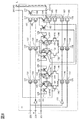
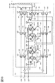
- the first sense amplifier and the second sense amplifier have a first power switch and a second power switch, respectively, and the first power switch has a p-channel transistor and a second power switch.
- the power switch may have an n-channel transistor, and the n-channel transistor may have a metal oxide in the channel forming region.
- the metal oxide preferably contains In, Zn, and M (M is one or more of Al, Ti, Ga, Ge, Sn, Y, Zr, La, Ce, Nd, or Hf).
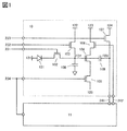
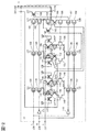
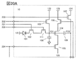
- the circuit 10 includes a photoelectric conversion device 101, a transistor 102, a transistor 103, a transistor 104, a transistor 105, a transistor 106, a transistor 107, a capacitor 108, and a capacitor 109.
- the capacitor 108 may be omitted.
- transistors 102 to 107 transistors having silicon in the channel forming region
- Si transistors transistors having silicon in the channel forming region
- Examples of the Si transistor include a transistor having amorphous silicon, a transistor having crystalline silicon (microcrystalline silicon, low temperature polysilicon, single crystal silicon), and the like. Si transistors have high mobility and are suitable for high-speed operation.
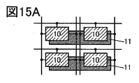
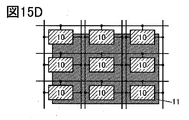
- Wiring 236, 234, and 237 are electrically connected to the circuit 11.
- Wiring 236, 234, and 237 are signal lines for controlling the continuity of the transistor.
- the transistor 106 of the circuit 10 is conducted. That is, the transistor 106, which is one of the two selection transistors of the circuit 10, can be forcibly conducted.
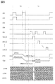
- the potential of the wiring 231 is set to "L”
- the potential of the wiring 233 is set to “L”
- the transistors 102 and 107 are non-conducting
- the potential of the node FD1 is held in "VRES1-Vref”.
- the potential of the node FD2 is held at "VRES2".
- VRES2 is a value obtained by replacing the data of the initial frame. The above is the description of the imaging operation of the initial frame.
- the transistor 105 conducts, and data corresponding to the potential of the node FD1 is output to the wiring 125.
- the above is the explanation of the reading operation of the initial frame.
- the data read here can be held in, for example, a frame memory.
- VRES1-Vtar1 is held in the node FD1.
- VRES2 + Vref-Vtar1 is held in the node FD2.
- VRES2 is the reset potential, but can be regarded as 0. Therefore, "+ Vref-Vtar1" is the difference itself between the data of the initial frame and the data acquired by the normal imaging operation.
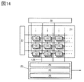
- FIG. 14 is a block diagram illustrating an imaging device according to an aspect of the present invention.
- the image pickup apparatus receives data from a pixel array 21 having pixels (circuit 10 and circuit 11) arranged in a matrix, a circuit 22 (low driver) having a function of selecting a row of the pixel array 21, and a circuit 10. It has a circuit 23 having a reading function and a circuit 28 for supplying a power supply potential.
- the number of wires connecting each element is simplified. Further, the number of circuits 22, 23, and 28 may be plural.
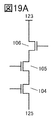
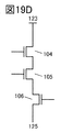
- the arrangement order of the transistors 104, 105, 106 connected in series with the wiring 123 and the wiring 125 may be the configuration shown in FIGS. 19A to 19E other than the configuration shown in FIG.
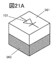
- the photoelectric conversion device 101 included in the layer 561 may be a laminate of the layer 566a, the layer 566b, the layer 566c, and the layer 566d.
- the photoelectric conversion device 101 shown in FIG. 22B is an example of an avalanche photodiode, in which layers 566a and 566d correspond to electrodes, and layers 566b and 566c correspond to photoelectric conversion units.
- a photoelectric conversion device using a selenium-based material has a characteristic of high external quantum efficiency with respect to visible light.
- the amplification of electrons with respect to the amount of incident light can be increased by utilizing the avalanche multiplication.
- the selenium-based material has a high light absorption coefficient, it has a production advantage such that the photoelectric conversion layer can be formed of a thin film.
- a thin film of a selenium-based material can be formed by a vacuum deposition method, a sputtering method, or the like.
- a transistor having an appropriate composition may be used according to the required semiconductor characteristics and electrical characteristics (field effect mobility, threshold voltage, etc.) of the transistor. Further, in order to obtain the required semiconductor characteristics of the transistor, it is preferable that the carrier density, impurity concentration, defect density, atomic number ratio of metal element and oxygen, interatomic distance, density and the like of the semiconductor layer are appropriate. ..
- CAC-OS in In-Ga-Zn oxide is indium oxide (hereinafter, InO).
- InO indium oxide
- X1 is a real number greater than 0
- In X2 Zn Y2 O Z2 X2, Y2, and Z2 are real numbers greater than 0
- the region in which GaO X3 or the like is the main component is a region having higher insulating property than the region in which In X2 Zn Y2 O Z2 or InO X1 is the main component. That is, since the region containing GaO X3 or the like as the main component is distributed in the oxide semiconductor, the leakage current can be suppressed and a good switching operation can be realized.
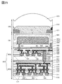
- the silicon substrate is provided with a groove for separating pixels, and the insulating layer 665 is provided on the upper surface of the silicon substrate and the groove.
- the insulating layer 665 By providing the insulating layer 665, it is possible to prevent the carriers generated in the photoelectric conversion device 101 from flowing out to the adjacent pixels.
- the insulating layer 665 also has a function of suppressing the intrusion of stray light. Therefore, the insulating layer 665 can suppress color mixing.
- An antireflection film may be provided between the upper surface of the silicon substrate and the insulating layer 665.
- Layer 562 is formed on layer 563.
- Layer 562 has an OS transistor.
- the transistor 102 and the transistor 106 are shown as part of the elements of the circuit 10. In the cross-sectional view shown in FIG. 26, the electrical connection between the two is not shown.
- an insulating layer 648 is formed on the insulating layer 626. Further, a conductive layer 688 electrically connected to one of the source or drain of the transistor 102 and a conductive layer 689 electrically connected to the conductive layer 627 are formed.
- the insulating layer 648 and the conductive layers 688 and 689 have a function as a bonding layer.
- the conductive layers 688 and 689 have a region embedded in the insulating layer 648. Further, the surfaces of the insulating layer 648 and the conductive layers 688 and 689 are flattened so that their heights match.
Landscapes
- Engineering & Computer Science (AREA)
- Multimedia (AREA)
- Signal Processing (AREA)
- Transforming Light Signals Into Electric Signals (AREA)
- Solid State Image Pick-Up Elements (AREA)
- Thin Film Transistor (AREA)
Priority Applications (6)
| Application Number | Priority Date | Filing Date | Title |
|---|---|---|---|
| CN202080077151.0A CN114641987A (zh) | 2019-11-07 | 2020-10-27 | 摄像装置、其工作方法及电子设备 |
| JP2021554423A JP7663507B2 (ja) | 2019-11-07 | 2020-10-27 | 撮像装置、電子機器 |
| KR1020227017275A KR20220093138A (ko) | 2019-11-07 | 2020-10-27 | 촬상 장치, 그 동작 방법, 및 전자 기기 |
| US17/768,972 US11917318B2 (en) | 2019-11-07 | 2020-10-27 | Imaging device, operation method thereof, and electronic device |
| US18/584,020 US12294805B2 (en) | 2019-11-07 | 2024-02-22 | Imaging device, operation method thereof, and electronic device |
| JP2025062238A JP7825762B2 (ja) | 2019-11-07 | 2025-04-04 | 撮像装置 |
Applications Claiming Priority (2)
| Application Number | Priority Date | Filing Date | Title |
|---|---|---|---|
| JP2019202403 | 2019-11-07 | ||
| JP2019-202403 | 2019-11-07 |
Related Child Applications (2)
| Application Number | Title | Priority Date | Filing Date |
|---|---|---|---|
| US17/768,972 A-371-Of-International US11917318B2 (en) | 2019-11-07 | 2020-10-27 | Imaging device, operation method thereof, and electronic device |
| US18/584,020 Continuation US12294805B2 (en) | 2019-11-07 | 2024-02-22 | Imaging device, operation method thereof, and electronic device |
Publications (1)
| Publication Number | Publication Date |
|---|---|
| WO2021090110A1 true WO2021090110A1 (ja) | 2021-05-14 |
Family
ID=75849815
Family Applications (1)
| Application Number | Title | Priority Date | Filing Date |
|---|---|---|---|
| PCT/IB2020/060041 Ceased WO2021090110A1 (ja) | 2019-11-07 | 2020-10-27 | 撮像装置、その動作方法および電子機器 |
Country Status (6)
| Country | Link |
|---|---|
| US (2) | US11917318B2 (https=) |
| JP (2) | JP7663507B2 (https=) |
| KR (1) | KR20220093138A (https=) |
| CN (1) | CN114641987A (https=) |
| TW (1) | TWI879824B (https=) |
| WO (1) | WO2021090110A1 (https=) |
Cited By (1)
| Publication number | Priority date | Publication date | Assignee | Title |
|---|---|---|---|---|
| US20240332164A1 (en) * | 2023-03-30 | 2024-10-03 | Ablic Inc. | Capacitive element and semiconductor device |
Families Citing this family (3)
| Publication number | Priority date | Publication date | Assignee | Title |
|---|---|---|---|---|
| KR20220093138A (ko) * | 2019-11-07 | 2022-07-05 | 가부시키가이샤 한도오따이 에네루기 켄큐쇼 | 촬상 장치, 그 동작 방법, 및 전자 기기 |
| US20240279455A1 (en) | 2021-10-22 | 2024-08-22 | Lg Chem, Ltd. | Thermoplastic resin composition, method of preparing the same, and molded article manufactured using the same |
| US12610147B2 (en) * | 2023-08-08 | 2026-04-21 | Qualcomm Incorporated | Automatic exposure control |
Citations (3)
| Publication number | Priority date | Publication date | Assignee | Title |
|---|---|---|---|---|
| JP2017005693A (ja) * | 2015-06-08 | 2017-01-05 | 株式会社半導体エネルギー研究所 | 撮像装置およびその動作方法、ならびに電子機器 |
| JP2017041878A (ja) * | 2015-08-19 | 2017-02-23 | 株式会社半導体エネルギー研究所 | 撮像装置およびその動作方法、ならびに電子機器 |
| WO2017158478A1 (ja) * | 2016-03-18 | 2017-09-21 | 株式会社半導体エネルギー研究所 | 撮像装置および電子機器 |
Family Cites Families (22)
| Publication number | Priority date | Publication date | Assignee | Title |
|---|---|---|---|---|
| US5376782A (en) | 1992-03-04 | 1994-12-27 | Fuji Xerox Co., Ltd. | Image pickup device providing decreased image lag |
| US5837995A (en) | 1996-11-25 | 1998-11-17 | Alan Y. Chow | Wavelength-controllable voltage-phase photodiode optoelectronic switch ("opsistor") |
| KR100677106B1 (ko) * | 2002-12-10 | 2007-02-01 | 삼성전자주식회사 | 정보저장매체 및 그 기록/재생방법 |
| US7623171B2 (en) | 2003-05-07 | 2009-11-24 | Aptina Imaging Corporation | Multiple crawbar switching in charge domain linear operations |
| CN104393007A (zh) | 2009-11-06 | 2015-03-04 | 株式会社半导体能源研究所 | 半导体装置 |
| CN102782622B (zh) | 2010-03-12 | 2016-11-02 | 株式会社半导体能源研究所 | 显示装置的驱动方法 |
| JP5651982B2 (ja) | 2010-03-31 | 2015-01-14 | ソニー株式会社 | 固体撮像装置、固体撮像装置の製造方法、及び電子機器 |
| JP2015119018A (ja) * | 2013-12-18 | 2015-06-25 | ソニー株式会社 | 固体撮像素子および電子機器 |
| KR102205702B1 (ko) * | 2014-07-30 | 2021-01-21 | 삼성전자주식회사 | 이미지 센서 및 이미지 센서를 구동하는 방법, 그리고 이를 이용한 영상 촬영 장치 |
| WO2016055909A1 (en) * | 2014-10-10 | 2016-04-14 | Semiconductor Energy Laboratory Co., Ltd. | Imaging device |
| JP6407083B2 (ja) | 2015-03-30 | 2018-10-17 | キヤノン株式会社 | 光電変換装置、および、光電変換システム |
| KR20160144314A (ko) | 2015-06-08 | 2016-12-16 | 가부시키가이샤 한도오따이 에네루기 켄큐쇼 | 촬상 장치 및 그 동작 방법, 및 전자 기기 |
| US10707260B2 (en) * | 2015-08-04 | 2020-07-07 | Artilux, Inc. | Circuit for operating a multi-gate VIS/IR photodiode |
| TWI608244B (zh) | 2015-08-07 | 2017-12-11 | 佳能股份有限公司 | 光電轉換設備、測距裝置、及資訊處理系統 |
| JP2017037938A (ja) | 2015-08-07 | 2017-02-16 | キヤノン株式会社 | 光電変換素子およびそれを用いた光電変換装置、距離検出用センサ並びに情報処理システム |
| US10205894B2 (en) | 2015-09-11 | 2019-02-12 | Canon Kabushiki Kaisha | Imaging device and imaging system |
| US10079990B2 (en) | 2016-09-27 | 2018-09-18 | Omnivision Technologies, Inc. | Comparator for double ramp analog to digital converter |
| JP6920652B2 (ja) * | 2017-02-03 | 2021-08-18 | パナソニックIpマネジメント株式会社 | 撮像装置 |
| TWI879128B (zh) | 2018-01-23 | 2025-04-01 | 日商索尼半導體解決方案公司 | 光檢測裝置 |
| JP2019176335A (ja) | 2018-03-28 | 2019-10-10 | ソニーセミコンダクタソリューションズ株式会社 | 固体撮像素子、撮像装置、および、固体撮像素子の制御方法 |
| WO2020075009A1 (ja) * | 2018-10-11 | 2020-04-16 | 株式会社半導体エネルギー研究所 | センサ装置および半導体装置 |
| KR20220093138A (ko) * | 2019-11-07 | 2022-07-05 | 가부시키가이샤 한도오따이 에네루기 켄큐쇼 | 촬상 장치, 그 동작 방법, 및 전자 기기 |
-
2020
- 2020-10-27 KR KR1020227017275A patent/KR20220093138A/ko active Pending
- 2020-10-27 CN CN202080077151.0A patent/CN114641987A/zh active Pending
- 2020-10-27 WO PCT/IB2020/060041 patent/WO2021090110A1/ja not_active Ceased
- 2020-10-27 US US17/768,972 patent/US11917318B2/en active Active
- 2020-10-27 JP JP2021554423A patent/JP7663507B2/ja active Active
- 2020-11-04 TW TW109138339A patent/TWI879824B/zh active
-
2024
- 2024-02-22 US US18/584,020 patent/US12294805B2/en active Active
-
2025
- 2025-04-04 JP JP2025062238A patent/JP7825762B2/ja active Active
Patent Citations (3)
| Publication number | Priority date | Publication date | Assignee | Title |
|---|---|---|---|---|
| JP2017005693A (ja) * | 2015-06-08 | 2017-01-05 | 株式会社半導体エネルギー研究所 | 撮像装置およびその動作方法、ならびに電子機器 |
| JP2017041878A (ja) * | 2015-08-19 | 2017-02-23 | 株式会社半導体エネルギー研究所 | 撮像装置およびその動作方法、ならびに電子機器 |
| WO2017158478A1 (ja) * | 2016-03-18 | 2017-09-21 | 株式会社半導体エネルギー研究所 | 撮像装置および電子機器 |
Cited By (1)
| Publication number | Priority date | Publication date | Assignee | Title |
|---|---|---|---|---|
| US20240332164A1 (en) * | 2023-03-30 | 2024-10-03 | Ablic Inc. | Capacitive element and semiconductor device |
Also Published As
| Publication number | Publication date |
|---|---|
| US11917318B2 (en) | 2024-02-27 |
| US12294805B2 (en) | 2025-05-06 |
| US20240196117A1 (en) | 2024-06-13 |
| JP7825762B2 (ja) | 2026-03-06 |
| KR20220093138A (ko) | 2022-07-05 |
| CN114641987A (zh) | 2022-06-17 |
| JP2025100583A (ja) | 2025-07-03 |
| JPWO2021090110A1 (https=) | 2021-05-14 |
| JP7663507B2 (ja) | 2025-04-16 |
| TWI879824B (zh) | 2025-04-11 |
| TW202139689A (zh) | 2021-10-16 |
| US20230247331A1 (en) | 2023-08-03 |
Similar Documents
| Publication | Publication Date | Title |
|---|---|---|
| JP7825762B2 (ja) | 撮像装置 | |
| JP2021027351A (ja) | 撮像装置および電子機器 | |
| JP7755695B2 (ja) | 撮像装置 | |
| JPWO2018229594A1 (ja) | 撮像装置、及び電子機器 | |
| WO2018185587A1 (ja) | 撮像装置および電子機器 | |
| JP2025072592A (ja) | 撮像装置 | |
| WO2021053449A1 (ja) | 撮像システムおよび電子機器 | |
| KR102837359B1 (ko) | 촬상 장치의 동작 방법 | |
| WO2021099889A1 (ja) | 撮像装置および電子機器 | |
| JP2021100025A (ja) | 撮像装置、撮像装置の駆動方法 | |
| JP7480137B2 (ja) | 撮像装置および電子機器 | |
| WO2021130590A1 (ja) | 撮像装置、および電子機器 | |
| WO2019243949A1 (ja) | 撮像装置の動作方法 | |
| JP2026074244A (ja) | 撮像装置 | |
| WO2021048676A1 (ja) | 撮像装置および電子機器 |
Legal Events
| Date | Code | Title | Description |
|---|---|---|---|
| 121 | Ep: the epo has been informed by wipo that ep was designated in this application |
Ref document number: 20886161 Country of ref document: EP Kind code of ref document: A1 |
|
| ENP | Entry into the national phase |
Ref document number: 2021554423 Country of ref document: JP Kind code of ref document: A |
|
| ENP | Entry into the national phase |
Ref document number: 20227017275 Country of ref document: KR Kind code of ref document: A |
|
| NENP | Non-entry into the national phase |
Ref country code: DE |
|
| 122 | Ep: pct application non-entry in european phase |
Ref document number: 20886161 Country of ref document: EP Kind code of ref document: A1 |