WO2021090110A1 - Image capture apparatus, operation method thereof, and electronic device - Google Patents
Image capture apparatus, operation method thereof, and electronic device Download PDFInfo
- Publication number
- WO2021090110A1 WO2021090110A1 PCT/IB2020/060041 IB2020060041W WO2021090110A1 WO 2021090110 A1 WO2021090110 A1 WO 2021090110A1 IB 2020060041 W IB2020060041 W IB 2020060041W WO 2021090110 A1 WO2021090110 A1 WO 2021090110A1
- Authority
- WO
- WIPO (PCT)
- Prior art keywords
- transistor
- circuit
- layer
- node
- voltage
- Prior art date
Links
- 238000000034 method Methods 0.000 title claims description 33
- 238000006243 chemical reaction Methods 0.000 claims description 77
- 238000003384 imaging method Methods 0.000 claims description 50
- 239000003990 capacitor Substances 0.000 claims description 30
- 229910052710 silicon Inorganic materials 0.000 claims description 28
- 239000010703 silicon Substances 0.000 claims description 28
- 229910052738 indium Inorganic materials 0.000 claims description 13
- 229910052782 aluminium Inorganic materials 0.000 claims description 12
- 229910052733 gallium Inorganic materials 0.000 claims description 12
- 229910044991 metal oxide Inorganic materials 0.000 claims description 12
- 150000004706 metal oxides Chemical class 0.000 claims description 12
- 229910052719 titanium Inorganic materials 0.000 claims description 9
- 229910052725 zinc Inorganic materials 0.000 claims description 9
- 229910052726 zirconium Inorganic materials 0.000 claims description 8
- 229910052684 Cerium Inorganic materials 0.000 claims description 7
- 229910052779 Neodymium Inorganic materials 0.000 claims description 7
- 229910052732 germanium Inorganic materials 0.000 claims description 7
- 229910052746 lanthanum Inorganic materials 0.000 claims description 7
- 229910052718 tin Inorganic materials 0.000 claims description 6
- 229910052727 yttrium Inorganic materials 0.000 claims description 6
- 230000000694 effects Effects 0.000 abstract description 4
- 239000010410 layer Substances 0.000 description 438
- 239000004065 semiconductor Substances 0.000 description 83
- 230000006870 function Effects 0.000 description 57
- 239000010408 film Substances 0.000 description 51
- 239000011701 zinc Substances 0.000 description 36
- 238000009413 insulation Methods 0.000 description 32
- XUIMIQQOPSSXEZ-UHFFFAOYSA-N Silicon Chemical compound [Si] XUIMIQQOPSSXEZ-UHFFFAOYSA-N 0.000 description 27
- 238000010586 diagram Methods 0.000 description 27
- 239000000758 substrate Substances 0.000 description 27
- 229910052751 metal Inorganic materials 0.000 description 20
- 239000000463 material Substances 0.000 description 17
- 239000002184 metal Substances 0.000 description 16
- 230000000875 corresponding effect Effects 0.000 description 15
- XLOMVQKBTHCTTD-UHFFFAOYSA-N Zinc monoxide Chemical compound [Zn]=O XLOMVQKBTHCTTD-UHFFFAOYSA-N 0.000 description 14
- 239000013078 crystal Substances 0.000 description 14
- UFHFLCQGNIYNRP-UHFFFAOYSA-N Hydrogen Chemical compound [H][H] UFHFLCQGNIYNRP-UHFFFAOYSA-N 0.000 description 12
- 239000001257 hydrogen Substances 0.000 description 12
- 229910052739 hydrogen Inorganic materials 0.000 description 12
- 229910000664 lithium aluminum titanium phosphates (LATP) Inorganic materials 0.000 description 12
- 230000003287 optical effect Effects 0.000 description 12
- BUGBHKTXTAQXES-UHFFFAOYSA-N Selenium Chemical compound [Se] BUGBHKTXTAQXES-UHFFFAOYSA-N 0.000 description 10
- 229910052711 selenium Inorganic materials 0.000 description 10
- 239000011669 selenium Substances 0.000 description 10
- 239000011787 zinc oxide Substances 0.000 description 8
- IJGRMHOSHXDMSA-UHFFFAOYSA-N Atomic nitrogen Chemical compound N#N IJGRMHOSHXDMSA-UHFFFAOYSA-N 0.000 description 7
- 238000004364 calculation method Methods 0.000 description 7
- 229910052802 copper Inorganic materials 0.000 description 7
- 239000010949 copper Substances 0.000 description 7
- 230000007547 defect Effects 0.000 description 7
- APFVFJFRJDLVQX-UHFFFAOYSA-N indium atom Chemical compound [In] APFVFJFRJDLVQX-UHFFFAOYSA-N 0.000 description 7
- 239000011229 interlayer Substances 0.000 description 7
- 238000010030 laminating Methods 0.000 description 7
- 239000000203 mixture Substances 0.000 description 7
- 239000010936 titanium Substances 0.000 description 7
- 229910052721 tungsten Inorganic materials 0.000 description 7
- GYHNNYVSQQEPJS-UHFFFAOYSA-N Gallium Chemical compound [Ga] GYHNNYVSQQEPJS-UHFFFAOYSA-N 0.000 description 6
- PXHVJJICTQNCMI-UHFFFAOYSA-N Nickel Chemical compound [Ni] PXHVJJICTQNCMI-UHFFFAOYSA-N 0.000 description 6
- XAGFODPZIPBFFR-UHFFFAOYSA-N aluminium Chemical compound [Al] XAGFODPZIPBFFR-UHFFFAOYSA-N 0.000 description 6
- 239000000969 carrier Substances 0.000 description 6
- 230000008859 change Effects 0.000 description 6
- 229910052760 oxygen Inorganic materials 0.000 description 6
- 230000001681 protective effect Effects 0.000 description 6
- 229910052814 silicon oxide Inorganic materials 0.000 description 6
- 238000004544 sputter deposition Methods 0.000 description 6
- RYGMFSIKBFXOCR-UHFFFAOYSA-N Copper Chemical compound [Cu] RYGMFSIKBFXOCR-UHFFFAOYSA-N 0.000 description 5
- 206010021143 Hypoxia Diseases 0.000 description 5
- 229910052581 Si3N4 Inorganic materials 0.000 description 5
- VYPSYNLAJGMNEJ-UHFFFAOYSA-N Silicium dioxide Chemical compound O=[Si]=O VYPSYNLAJGMNEJ-UHFFFAOYSA-N 0.000 description 5
- RTAQQCXQSZGOHL-UHFFFAOYSA-N Titanium Chemical compound [Ti] RTAQQCXQSZGOHL-UHFFFAOYSA-N 0.000 description 5
- 230000000903 blocking effect Effects 0.000 description 5
- 150000001875 compounds Chemical class 0.000 description 5
- 239000004020 conductor Substances 0.000 description 5
- 230000001276 controlling effect Effects 0.000 description 5
- 229910052735 hafnium Inorganic materials 0.000 description 5
- 238000004519 manufacturing process Methods 0.000 description 5
- 230000004048 modification Effects 0.000 description 5
- 238000012986 modification Methods 0.000 description 5
- 238000000926 separation method Methods 0.000 description 5
- HQVNEWCFYHHQES-UHFFFAOYSA-N silicon nitride Chemical compound N12[Si]34N5[Si]62N3[Si]51N64 HQVNEWCFYHHQES-UHFFFAOYSA-N 0.000 description 5
- 238000003860 storage Methods 0.000 description 5
- WFKWXMTUELFFGS-UHFFFAOYSA-N tungsten Chemical compound [W] WFKWXMTUELFFGS-UHFFFAOYSA-N 0.000 description 5
- 239000010937 tungsten Substances 0.000 description 5
- -1 C 60 and C 70 Chemical class 0.000 description 4
- XEEYBQQBJWHFJM-UHFFFAOYSA-N Iron Chemical compound [Fe] XEEYBQQBJWHFJM-UHFFFAOYSA-N 0.000 description 4
- QCWXUUIWCKQGHC-UHFFFAOYSA-N Zirconium Chemical compound [Zr] QCWXUUIWCKQGHC-UHFFFAOYSA-N 0.000 description 4
- QVGXLLKOCUKJST-UHFFFAOYSA-N atomic oxygen Chemical compound [O] QVGXLLKOCUKJST-UHFFFAOYSA-N 0.000 description 4
- AJNVQOSZGJRYEI-UHFFFAOYSA-N digallium;oxygen(2-) Chemical compound [O-2].[O-2].[O-2].[Ga+3].[Ga+3] AJNVQOSZGJRYEI-UHFFFAOYSA-N 0.000 description 4
- 229910001195 gallium oxide Inorganic materials 0.000 description 4
- 239000010931 gold Substances 0.000 description 4
- VBJZVLUMGGDVMO-UHFFFAOYSA-N hafnium atom Chemical compound [Hf] VBJZVLUMGGDVMO-UHFFFAOYSA-N 0.000 description 4
- 238000005304 joining Methods 0.000 description 4
- 239000001301 oxygen Substances 0.000 description 4
- 238000005498 polishing Methods 0.000 description 4
- 230000008569 process Effects 0.000 description 4
- 230000005855 radiation Effects 0.000 description 4
- 238000001004 secondary ion mass spectrometry Methods 0.000 description 4
- 229910052715 tantalum Inorganic materials 0.000 description 4
- GUVRBAGPIYLISA-UHFFFAOYSA-N tantalum atom Chemical compound [Ta] GUVRBAGPIYLISA-UHFFFAOYSA-N 0.000 description 4
- 239000010409 thin film Substances 0.000 description 4
- OKTJSMMVPCPJKN-UHFFFAOYSA-N Carbon Chemical compound [C] OKTJSMMVPCPJKN-UHFFFAOYSA-N 0.000 description 3
- MYMOFIZGZYHOMD-UHFFFAOYSA-N Dioxygen Chemical compound O=O MYMOFIZGZYHOMD-UHFFFAOYSA-N 0.000 description 3
- FYYHWMGAXLPEAU-UHFFFAOYSA-N Magnesium Chemical compound [Mg] FYYHWMGAXLPEAU-UHFFFAOYSA-N 0.000 description 3
- ZOKXTWBITQBERF-UHFFFAOYSA-N Molybdenum Chemical compound [Mo] ZOKXTWBITQBERF-UHFFFAOYSA-N 0.000 description 3
- 239000000853 adhesive Substances 0.000 description 3
- 229910052790 beryllium Inorganic materials 0.000 description 3
- ATBAMAFKBVZNFJ-UHFFFAOYSA-N beryllium atom Chemical compound [Be] ATBAMAFKBVZNFJ-UHFFFAOYSA-N 0.000 description 3
- 230000015572 biosynthetic process Effects 0.000 description 3
- ZMIGMASIKSOYAM-UHFFFAOYSA-N cerium Chemical compound [Ce][Ce][Ce][Ce][Ce][Ce][Ce][Ce][Ce][Ce][Ce][Ce][Ce][Ce][Ce][Ce][Ce][Ce][Ce][Ce][Ce][Ce][Ce][Ce][Ce][Ce][Ce][Ce][Ce][Ce][Ce][Ce][Ce][Ce][Ce][Ce][Ce][Ce] ZMIGMASIKSOYAM-UHFFFAOYSA-N 0.000 description 3
- 239000006059 cover glass Substances 0.000 description 3
- 229910001882 dioxygen Inorganic materials 0.000 description 3
- 238000002149 energy-dispersive X-ray emission spectroscopy Methods 0.000 description 3
- 230000005669 field effect Effects 0.000 description 3
- GNPVGFCGXDBREM-UHFFFAOYSA-N germanium atom Chemical compound [Ge] GNPVGFCGXDBREM-UHFFFAOYSA-N 0.000 description 3
- 239000012535 impurity Substances 0.000 description 3
- 229910003437 indium oxide Inorganic materials 0.000 description 3
- PJXISJQVUVHSOJ-UHFFFAOYSA-N indium(iii) oxide Chemical compound [O-2].[O-2].[O-2].[In+3].[In+3] PJXISJQVUVHSOJ-UHFFFAOYSA-N 0.000 description 3
- FZLIPJUXYLNCLC-UHFFFAOYSA-N lanthanum atom Chemical compound [La] FZLIPJUXYLNCLC-UHFFFAOYSA-N 0.000 description 3
- 229910052749 magnesium Inorganic materials 0.000 description 3
- 239000011777 magnesium Substances 0.000 description 3
- 229910052750 molybdenum Inorganic materials 0.000 description 3
- 239000011733 molybdenum Substances 0.000 description 3
- 229910021421 monocrystalline silicon Inorganic materials 0.000 description 3
- 239000002105 nanoparticle Substances 0.000 description 3
- QEFYFXOXNSNQGX-UHFFFAOYSA-N neodymium atom Chemical compound [Nd] QEFYFXOXNSNQGX-UHFFFAOYSA-N 0.000 description 3
- 229910052759 nickel Inorganic materials 0.000 description 3
- 229910052757 nitrogen Inorganic materials 0.000 description 3
- TWNQGVIAIRXVLR-UHFFFAOYSA-N oxo(oxoalumanyloxy)alumane Chemical compound O=[Al]O[Al]=O TWNQGVIAIRXVLR-UHFFFAOYSA-N 0.000 description 3
- BASFCYQUMIYNBI-UHFFFAOYSA-N platinum Chemical compound [Pt] BASFCYQUMIYNBI-UHFFFAOYSA-N 0.000 description 3
- 238000012545 processing Methods 0.000 description 3
- 229910052709 silver Inorganic materials 0.000 description 3
- 238000005477 sputtering target Methods 0.000 description 3
- 229910052720 vanadium Inorganic materials 0.000 description 3
- GPPXJZIENCGNKB-UHFFFAOYSA-N vanadium Chemical compound [V]#[V] GPPXJZIENCGNKB-UHFFFAOYSA-N 0.000 description 3
- VUFNLQXQSDUXKB-DOFZRALJSA-N 2-[4-[4-[bis(2-chloroethyl)amino]phenyl]butanoyloxy]ethyl (5z,8z,11z,14z)-icosa-5,8,11,14-tetraenoate Chemical group CCCCC\C=C/C\C=C/C\C=C/C\C=C/CCCC(=O)OCCOC(=O)CCCC1=CC=C(N(CCCl)CCCl)C=C1 VUFNLQXQSDUXKB-DOFZRALJSA-N 0.000 description 2
- XKRFYHLGVUSROY-UHFFFAOYSA-N Argon Chemical compound [Ar] XKRFYHLGVUSROY-UHFFFAOYSA-N 0.000 description 2
- ZOXJGFHDIHLPTG-UHFFFAOYSA-N Boron Chemical compound [B] ZOXJGFHDIHLPTG-UHFFFAOYSA-N 0.000 description 2
- 229910052688 Gadolinium Inorganic materials 0.000 description 2
- BQCADISMDOOEFD-UHFFFAOYSA-N Silver Chemical compound [Ag] BQCADISMDOOEFD-UHFFFAOYSA-N 0.000 description 2
- 238000002441 X-ray diffraction Methods 0.000 description 2
- HCHKCACWOHOZIP-UHFFFAOYSA-N Zinc Chemical compound [Zn] HCHKCACWOHOZIP-UHFFFAOYSA-N 0.000 description 2
- 230000001070 adhesive effect Effects 0.000 description 2
- 229910052783 alkali metal Inorganic materials 0.000 description 2
- 150000001340 alkali metals Chemical class 0.000 description 2
- 229910052784 alkaline earth metal Inorganic materials 0.000 description 2
- 150000001342 alkaline earth metals Chemical class 0.000 description 2
- 238000000231 atomic layer deposition Methods 0.000 description 2
- 229910052796 boron Inorganic materials 0.000 description 2
- 229910052799 carbon Inorganic materials 0.000 description 2
- 239000002131 composite material Substances 0.000 description 2
- 230000008878 coupling Effects 0.000 description 2
- 238000010168 coupling process Methods 0.000 description 2
- 238000005859 coupling reaction Methods 0.000 description 2
- 238000009792 diffusion process Methods 0.000 description 2
- 238000010894 electron beam technology Methods 0.000 description 2
- 238000002524 electron diffraction data Methods 0.000 description 2
- 239000007789 gas Substances 0.000 description 2
- 239000011521 glass Substances 0.000 description 2
- 229910052737 gold Inorganic materials 0.000 description 2
- 229910000449 hafnium oxide Inorganic materials 0.000 description 2
- WIHZLLGSGQNAGK-UHFFFAOYSA-N hafnium(4+);oxygen(2-) Chemical compound [O-2].[O-2].[Hf+4] WIHZLLGSGQNAGK-UHFFFAOYSA-N 0.000 description 2
- 230000005525 hole transport Effects 0.000 description 2
- 239000011810 insulating material Substances 0.000 description 2
- 229910052742 iron Inorganic materials 0.000 description 2
- 239000007769 metal material Substances 0.000 description 2
- 239000013081 microcrystal Substances 0.000 description 2
- 239000002159 nanocrystal Substances 0.000 description 2
- SIWVEOZUMHYXCS-UHFFFAOYSA-N oxo(oxoyttriooxy)yttrium Chemical compound O=[Y]O[Y]=O SIWVEOZUMHYXCS-UHFFFAOYSA-N 0.000 description 2
- 229910052697 platinum Inorganic materials 0.000 description 2
- 229920001721 polyimide Polymers 0.000 description 2
- 239000011347 resin Substances 0.000 description 2
- 229920005989 resin Polymers 0.000 description 2
- 238000005070 sampling Methods 0.000 description 2
- 229940065287 selenium compound Drugs 0.000 description 2
- 150000003343 selenium compounds Chemical class 0.000 description 2
- 239000004332 silver Substances 0.000 description 2
- 239000002356 single layer Substances 0.000 description 2
- 239000002344 surface layer Substances 0.000 description 2
- XOLBLPGZBRYERU-UHFFFAOYSA-N tin dioxide Chemical compound O=[Sn]=O XOLBLPGZBRYERU-UHFFFAOYSA-N 0.000 description 2
- 229910001887 tin oxide Inorganic materials 0.000 description 2
- 229910001233 yttria-stabilized zirconia Inorganic materials 0.000 description 2
- VWQVUPCCIRVNHF-UHFFFAOYSA-N yttrium atom Chemical compound [Y] VWQVUPCCIRVNHF-UHFFFAOYSA-N 0.000 description 2
- 239000004925 Acrylic resin Substances 0.000 description 1
- 229920000178 Acrylic resin Polymers 0.000 description 1
- 229910016036 BaF 2 Inorganic materials 0.000 description 1
- XMWRBQBLMFGWIX-UHFFFAOYSA-N C60 fullerene Chemical class C12=C3C(C4=C56)=C7C8=C5C5=C9C%10=C6C6=C4C1=C1C4=C6C6=C%10C%10=C9C9=C%11C5=C8C5=C8C7=C3C3=C7C2=C1C1=C2C4=C6C4=C%10C6=C9C9=C%11C5=C5C8=C3C3=C7C1=C1C2=C4C6=C2C9=C5C3=C12 XMWRBQBLMFGWIX-UHFFFAOYSA-N 0.000 description 1
- 229910004261 CaF 2 Inorganic materials 0.000 description 1
- 229910020156 CeF Inorganic materials 0.000 description 1
- VYZAMTAEIAYCRO-UHFFFAOYSA-N Chromium Chemical compound [Cr] VYZAMTAEIAYCRO-UHFFFAOYSA-N 0.000 description 1
- 239000004642 Polyimide Substances 0.000 description 1
- 229910052777 Praseodymium Inorganic materials 0.000 description 1
- KJTLSVCANCCWHF-UHFFFAOYSA-N Ruthenium Chemical compound [Ru] KJTLSVCANCCWHF-UHFFFAOYSA-N 0.000 description 1
- 229910052771 Terbium Inorganic materials 0.000 description 1
- ATJFFYVFTNAWJD-UHFFFAOYSA-N Tin Chemical compound [Sn] ATJFFYVFTNAWJD-UHFFFAOYSA-N 0.000 description 1
- NRTOMJZYCJJWKI-UHFFFAOYSA-N Titanium nitride Chemical compound [Ti]#N NRTOMJZYCJJWKI-UHFFFAOYSA-N 0.000 description 1
- NIXOWILDQLNWCW-UHFFFAOYSA-N acrylic acid group Chemical group C(C=C)(=O)O NIXOWILDQLNWCW-UHFFFAOYSA-N 0.000 description 1
- 230000004913 activation Effects 0.000 description 1
- 229910021417 amorphous silicon Inorganic materials 0.000 description 1
- 230000003321 amplification Effects 0.000 description 1
- 239000003963 antioxidant agent Substances 0.000 description 1
- 230000003078 antioxidant effect Effects 0.000 description 1
- 229910052786 argon Inorganic materials 0.000 description 1
- 238000013528 artificial neural network Methods 0.000 description 1
- 239000002585 base Substances 0.000 description 1
- 230000008901 benefit Effects 0.000 description 1
- XQPRBTXUXXVTKB-UHFFFAOYSA-M caesium iodide Inorganic materials [I-].[Cs+] XQPRBTXUXXVTKB-UHFFFAOYSA-M 0.000 description 1
- 229910052800 carbon group element Inorganic materials 0.000 description 1
- 230000015556 catabolic process Effects 0.000 description 1
- 239000000919 ceramic Substances 0.000 description 1
- 238000005229 chemical vapour deposition Methods 0.000 description 1
- 229910052804 chromium Inorganic materials 0.000 description 1
- 239000011651 chromium Substances 0.000 description 1
- 239000003086 colorant Substances 0.000 description 1
- 238000004891 communication Methods 0.000 description 1
- 239000000470 constituent Substances 0.000 description 1
- PMHQVHHXPFUNSP-UHFFFAOYSA-M copper(1+);methylsulfanylmethane;bromide Chemical compound Br[Cu].CSC PMHQVHHXPFUNSP-UHFFFAOYSA-M 0.000 description 1
- 230000002596 correlated effect Effects 0.000 description 1
- 229910021419 crystalline silicon Inorganic materials 0.000 description 1
- 230000018044 dehydration Effects 0.000 description 1
- 238000006297 dehydration reaction Methods 0.000 description 1
- 230000006866 deterioration Effects 0.000 description 1
- 229910001873 dinitrogen Inorganic materials 0.000 description 1
- 230000005684 electric field Effects 0.000 description 1
- 238000000605 extraction Methods 0.000 description 1
- 238000007667 floating Methods 0.000 description 1
- 229910003472 fullerene Inorganic materials 0.000 description 1
- PCHJSUWPFVWCPO-UHFFFAOYSA-N gold Chemical compound [Au] PCHJSUWPFVWCPO-UHFFFAOYSA-N 0.000 description 1
- 229910021389 graphene Inorganic materials 0.000 description 1
- 230000012447 hatching Effects 0.000 description 1
- 238000010438 heat treatment Methods 0.000 description 1
- AMGQUBHHOARCQH-UHFFFAOYSA-N indium;oxotin Chemical compound [In].[Sn]=O AMGQUBHHOARCQH-UHFFFAOYSA-N 0.000 description 1
- 239000011261 inert gas Substances 0.000 description 1
- 238000003331 infrared imaging Methods 0.000 description 1
- 238000002347 injection Methods 0.000 description 1
- 239000007924 injection Substances 0.000 description 1
- 239000012212 insulator Substances 0.000 description 1
- 229910052741 iridium Inorganic materials 0.000 description 1
- GKOZUEZYRPOHIO-UHFFFAOYSA-N iridium atom Chemical compound [Ir] GKOZUEZYRPOHIO-UHFFFAOYSA-N 0.000 description 1
- 230000001678 irradiating effect Effects 0.000 description 1
- 238000002955 isolation Methods 0.000 description 1
- 230000002045 lasting effect Effects 0.000 description 1
- 230000031700 light absorption Effects 0.000 description 1
- 239000004973 liquid crystal related substance Substances 0.000 description 1
- WPBNNNQJVZRUHP-UHFFFAOYSA-L manganese(2+);methyl n-[[2-(methoxycarbonylcarbamothioylamino)phenyl]carbamothioyl]carbamate;n-[2-(sulfidocarbothioylamino)ethyl]carbamodithioate Chemical compound [Mn+2].[S-]C(=S)NCCNC([S-])=S.COC(=O)NC(=S)NC1=CC=CC=C1NC(=S)NC(=O)OC WPBNNNQJVZRUHP-UHFFFAOYSA-L 0.000 description 1
- 238000013507 mapping Methods 0.000 description 1
- 239000011159 matrix material Substances 0.000 description 1
- 238000005259 measurement Methods 0.000 description 1
- 238000000691 measurement method Methods 0.000 description 1
- 230000007246 mechanism Effects 0.000 description 1
- 150000002739 metals Chemical class 0.000 description 1
- 229910021424 microcrystalline silicon Inorganic materials 0.000 description 1
- 238000002156 mixing Methods 0.000 description 1
- 229910000476 molybdenum oxide Inorganic materials 0.000 description 1
- 229910052758 niobium Inorganic materials 0.000 description 1
- 239000010955 niobium Substances 0.000 description 1
- GUCVJGMIXFAOAE-UHFFFAOYSA-N niobium atom Chemical compound [Nb] GUCVJGMIXFAOAE-UHFFFAOYSA-N 0.000 description 1
- 238000003199 nucleic acid amplification method Methods 0.000 description 1
- PQQKPALAQIIWST-UHFFFAOYSA-N oxomolybdenum Chemical compound [Mo]=O PQQKPALAQIIWST-UHFFFAOYSA-N 0.000 description 1
- 239000002245 particle Substances 0.000 description 1
- 238000005424 photoluminescence Methods 0.000 description 1
- 229910021420 polycrystalline silicon Inorganic materials 0.000 description 1
- 239000009719 polyimide resin Substances 0.000 description 1
- 229920005591 polysilicon Polymers 0.000 description 1
- 238000011084 recovery Methods 0.000 description 1
- 239000003870 refractory metal Substances 0.000 description 1
- 229910052707 ruthenium Inorganic materials 0.000 description 1
- 239000000523 sample Substances 0.000 description 1
- 239000010944 silver (metal) Substances 0.000 description 1
- FVAUCKIRQBBSSJ-UHFFFAOYSA-M sodium iodide Inorganic materials [Na+].[I-] FVAUCKIRQBBSSJ-UHFFFAOYSA-M 0.000 description 1
- 229910000679 solder Inorganic materials 0.000 description 1
- 238000001179 sorption measurement Methods 0.000 description 1
- 229910052712 strontium Inorganic materials 0.000 description 1
- CIOAGBVUUVVLOB-UHFFFAOYSA-N strontium atom Chemical compound [Sr] CIOAGBVUUVVLOB-UHFFFAOYSA-N 0.000 description 1
- 239000000126 substance Substances 0.000 description 1
- 238000001771 vacuum deposition Methods 0.000 description 1
- XLYOFNOQVPJJNP-UHFFFAOYSA-N water Substances O XLYOFNOQVPJJNP-UHFFFAOYSA-N 0.000 description 1
- YVTHLONGBIQYBO-UHFFFAOYSA-N zinc indium(3+) oxygen(2-) Chemical compound [O--].[Zn++].[In+3] YVTHLONGBIQYBO-UHFFFAOYSA-N 0.000 description 1
Images


Classifications
-
- H—ELECTRICITY
- H04—ELECTRIC COMMUNICATION TECHNIQUE
- H04N—PICTORIAL COMMUNICATION, e.g. TELEVISION
- H04N25/00—Circuitry of solid-state image sensors [SSIS]; Control thereof
- H04N25/70—SSIS architectures; Circuits associated therewith
- H04N25/76—Addressed sensors, e.g. MOS or CMOS sensors
- H04N25/77—Pixel circuitry, e.g. memories, A/D converters, pixel amplifiers, shared circuits or shared components
-
- H—ELECTRICITY
- H04—ELECTRIC COMMUNICATION TECHNIQUE
- H04N—PICTORIAL COMMUNICATION, e.g. TELEVISION
- H04N25/00—Circuitry of solid-state image sensors [SSIS]; Control thereof
- H04N25/47—Image sensors with pixel address output; Event-driven image sensors; Selection of pixels to be read out based on image data
-
- H—ELECTRICITY
- H04—ELECTRIC COMMUNICATION TECHNIQUE
- H04N—PICTORIAL COMMUNICATION, e.g. TELEVISION
- H04N25/00—Circuitry of solid-state image sensors [SSIS]; Control thereof
- H04N25/70—SSIS architectures; Circuits associated therewith
- H04N25/703—SSIS architectures incorporating pixels for producing signals other than image signals
- H04N25/707—Pixels for event detection
-
- H—ELECTRICITY
- H04—ELECTRIC COMMUNICATION TECHNIQUE
- H04N—PICTORIAL COMMUNICATION, e.g. TELEVISION
- H04N25/00—Circuitry of solid-state image sensors [SSIS]; Control thereof
- H04N25/70—SSIS architectures; Circuits associated therewith
- H04N25/709—Circuitry for control of the power supply
-
- H—ELECTRICITY
- H04—ELECTRIC COMMUNICATION TECHNIQUE
- H04N—PICTORIAL COMMUNICATION, e.g. TELEVISION
- H04N25/00—Circuitry of solid-state image sensors [SSIS]; Control thereof
- H04N25/70—SSIS architectures; Circuits associated therewith
- H04N25/76—Addressed sensors, e.g. MOS or CMOS sensors
- H04N25/78—Readout circuits for addressed sensors, e.g. output amplifiers or A/D converters
-
- H—ELECTRICITY
- H10—SEMICONDUCTOR DEVICES; ELECTRIC SOLID-STATE DEVICES NOT OTHERWISE PROVIDED FOR
- H10D—INORGANIC ELECTRIC SEMICONDUCTOR DEVICES
- H10D30/00—Field-effect transistors [FET]
- H10D30/60—Insulated-gate field-effect transistors [IGFET]
- H10D30/67—Thin-film transistors [TFT]
-
- H—ELECTRICITY
- H10—SEMICONDUCTOR DEVICES; ELECTRIC SOLID-STATE DEVICES NOT OTHERWISE PROVIDED FOR
- H10F—INORGANIC SEMICONDUCTOR DEVICES SENSITIVE TO INFRARED RADIATION, LIGHT, ELECTROMAGNETIC RADIATION OF SHORTER WAVELENGTH OR CORPUSCULAR RADIATION
- H10F39/00—Integrated devices, or assemblies of multiple devices, comprising at least one element covered by group H10F30/00, e.g. radiation detectors comprising photodiode arrays
- H10F39/10—Integrated devices
- H10F39/12—Image sensors
-
- H—ELECTRICITY
- H10—SEMICONDUCTOR DEVICES; ELECTRIC SOLID-STATE DEVICES NOT OTHERWISE PROVIDED FOR
- H10F—INORGANIC SEMICONDUCTOR DEVICES SENSITIVE TO INFRARED RADIATION, LIGHT, ELECTROMAGNETIC RADIATION OF SHORTER WAVELENGTH OR CORPUSCULAR RADIATION
- H10F39/00—Integrated devices, or assemblies of multiple devices, comprising at least one element covered by group H10F30/00, e.g. radiation detectors comprising photodiode arrays
- H10F39/80—Constructional details of image sensors
- H10F39/803—Pixels having integrated switching, control, storage or amplification elements
- H10F39/8037—Pixels having integrated switching, control, storage or amplification elements the integrated elements comprising a transistor
-
- H—ELECTRICITY
- H10—SEMICONDUCTOR DEVICES; ELECTRIC SOLID-STATE DEVICES NOT OTHERWISE PROVIDED FOR
- H10F—INORGANIC SEMICONDUCTOR DEVICES SENSITIVE TO INFRARED RADIATION, LIGHT, ELECTROMAGNETIC RADIATION OF SHORTER WAVELENGTH OR CORPUSCULAR RADIATION
- H10F39/00—Integrated devices, or assemblies of multiple devices, comprising at least one element covered by group H10F30/00, e.g. radiation detectors comprising photodiode arrays
- H10F39/80—Constructional details of image sensors
- H10F39/811—Interconnections
-
- H—ELECTRICITY
- H10—SEMICONDUCTOR DEVICES; ELECTRIC SOLID-STATE DEVICES NOT OTHERWISE PROVIDED FOR
- H10K—ORGANIC ELECTRIC SOLID-STATE DEVICES
- H10K39/00—Integrated devices, or assemblies of multiple devices, comprising at least one organic radiation-sensitive element covered by group H10K30/00
- H10K39/30—Devices controlled by radiation
- H10K39/32—Organic image sensors
-
- H—ELECTRICITY
- H10—SEMICONDUCTOR DEVICES; ELECTRIC SOLID-STATE DEVICES NOT OTHERWISE PROVIDED FOR
- H10K—ORGANIC ELECTRIC SOLID-STATE DEVICES
- H10K30/00—Organic devices sensitive to infrared radiation, light, electromagnetic radiation of shorter wavelength or corpuscular radiation
- H10K30/30—Organic devices sensitive to infrared radiation, light, electromagnetic radiation of shorter wavelength or corpuscular radiation comprising bulk heterojunctions, e.g. interpenetrating networks of donor and acceptor material domains
Definitions
- the first sense amplifier and the second sense amplifier have a first power switch and a second power switch, respectively, and the first power switch has a p-channel transistor and a second power switch.
- the power switch may have an n-channel transistor, and the n-channel transistor may have a metal oxide in the channel forming region.
- the metal oxide preferably contains In, Zn, and M (M is one or more of Al, Ti, Ga, Ge, Sn, Y, Zr, La, Ce, Nd, or Hf).
- the circuit 10 includes a photoelectric conversion device 101, a transistor 102, a transistor 103, a transistor 104, a transistor 105, a transistor 106, a transistor 107, a capacitor 108, and a capacitor 109.
- the capacitor 108 may be omitted.
- transistors 102 to 107 transistors having silicon in the channel forming region
- Si transistors transistors having silicon in the channel forming region
- Examples of the Si transistor include a transistor having amorphous silicon, a transistor having crystalline silicon (microcrystalline silicon, low temperature polysilicon, single crystal silicon), and the like. Si transistors have high mobility and are suitable for high-speed operation.
- Wiring 236, 234, and 237 are electrically connected to the circuit 11.
- Wiring 236, 234, and 237 are signal lines for controlling the continuity of the transistor.
- the transistor 106 of the circuit 10 is conducted. That is, the transistor 106, which is one of the two selection transistors of the circuit 10, can be forcibly conducted.
- the potential of the wiring 231 is set to "L”
- the potential of the wiring 233 is set to “L”
- the transistors 102 and 107 are non-conducting
- the potential of the node FD1 is held in "VRES1-Vref”.
- the potential of the node FD2 is held at "VRES2".
- VRES2 is a value obtained by replacing the data of the initial frame. The above is the description of the imaging operation of the initial frame.
- the transistor 105 conducts, and data corresponding to the potential of the node FD1 is output to the wiring 125.
- the above is the explanation of the reading operation of the initial frame.
- the data read here can be held in, for example, a frame memory.
- VRES1-Vtar1 is held in the node FD1.
- VRES2 + Vref-Vtar1 is held in the node FD2.
- VRES2 is the reset potential, but can be regarded as 0. Therefore, "+ Vref-Vtar1" is the difference itself between the data of the initial frame and the data acquired by the normal imaging operation.
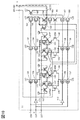
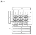
- FIG. 14 is a block diagram illustrating an imaging device according to an aspect of the present invention.
- the image pickup apparatus receives data from a pixel array 21 having pixels (circuit 10 and circuit 11) arranged in a matrix, a circuit 22 (low driver) having a function of selecting a row of the pixel array 21, and a circuit 10. It has a circuit 23 having a reading function and a circuit 28 for supplying a power supply potential.
- the number of wires connecting each element is simplified. Further, the number of circuits 22, 23, and 28 may be plural.
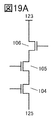
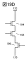
- the arrangement order of the transistors 104, 105, 106 connected in series with the wiring 123 and the wiring 125 may be the configuration shown in FIGS. 19A to 19E other than the configuration shown in FIG.
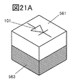
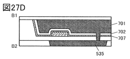
- the photoelectric conversion device 101 included in the layer 561 may be a laminate of the layer 566a, the layer 566b, the layer 566c, and the layer 566d.
- the photoelectric conversion device 101 shown in FIG. 22B is an example of an avalanche photodiode, in which layers 566a and 566d correspond to electrodes, and layers 566b and 566c correspond to photoelectric conversion units.
- a photoelectric conversion device using a selenium-based material has a characteristic of high external quantum efficiency with respect to visible light.
- the amplification of electrons with respect to the amount of incident light can be increased by utilizing the avalanche multiplication.
- the selenium-based material has a high light absorption coefficient, it has a production advantage such that the photoelectric conversion layer can be formed of a thin film.
- a thin film of a selenium-based material can be formed by a vacuum deposition method, a sputtering method, or the like.
- a transistor having an appropriate composition may be used according to the required semiconductor characteristics and electrical characteristics (field effect mobility, threshold voltage, etc.) of the transistor. Further, in order to obtain the required semiconductor characteristics of the transistor, it is preferable that the carrier density, impurity concentration, defect density, atomic number ratio of metal element and oxygen, interatomic distance, density and the like of the semiconductor layer are appropriate. ..
- CAC-OS in In-Ga-Zn oxide is indium oxide (hereinafter, InO).
- InO indium oxide
- X1 is a real number greater than 0
- In X2 Zn Y2 O Z2 X2, Y2, and Z2 are real numbers greater than 0
- the region in which GaO X3 or the like is the main component is a region having higher insulating property than the region in which In X2 Zn Y2 O Z2 or InO X1 is the main component. That is, since the region containing GaO X3 or the like as the main component is distributed in the oxide semiconductor, the leakage current can be suppressed and a good switching operation can be realized.
- the silicon substrate is provided with a groove for separating pixels, and the insulating layer 665 is provided on the upper surface of the silicon substrate and the groove.
- the insulating layer 665 By providing the insulating layer 665, it is possible to prevent the carriers generated in the photoelectric conversion device 101 from flowing out to the adjacent pixels.
- the insulating layer 665 also has a function of suppressing the intrusion of stray light. Therefore, the insulating layer 665 can suppress color mixing.
- An antireflection film may be provided between the upper surface of the silicon substrate and the insulating layer 665.
- Layer 562 is formed on layer 563.
- Layer 562 has an OS transistor.
- the transistor 102 and the transistor 106 are shown as part of the elements of the circuit 10. In the cross-sectional view shown in FIG. 26, the electrical connection between the two is not shown.
- an insulating layer 648 is formed on the insulating layer 626. Further, a conductive layer 688 electrically connected to one of the source or drain of the transistor 102 and a conductive layer 689 electrically connected to the conductive layer 627 are formed.
- the insulating layer 648 and the conductive layers 688 and 689 have a function as a bonding layer.
- the conductive layers 688 and 689 have a region embedded in the insulating layer 648. Further, the surfaces of the insulating layer 648 and the conductive layers 688 and 689 are flattened so that their heights match.
Landscapes
- Engineering & Computer Science (AREA)
- Multimedia (AREA)
- Signal Processing (AREA)
- Thin Film Transistor (AREA)
- Solid State Image Pick-Up Elements (AREA)
- Transforming Light Signals Into Electric Signals (AREA)
Abstract
Description
本発明の一態様は、撮像装置に関する。 One aspect of the present invention relates to an imaging device.
なお、本発明の一態様は、上記の技術分野に限定されない。本明細書等で開示する発明の一態様の技術分野は、物、方法、または、製造方法に関するものである。または、本発明の一態様は、プロセス、マシン、マニュファクチャ、または、組成物(コンポジション・オブ・マター)に関するものである。そのため、より具体的に本明細書で開示する本発明の一態様の技術分野としては、半導体装置、表示装置、液晶表示装置、発光装置、照明装置、蓄電装置、記憶装置、撮像装置、それらの動作方法、または、それらの製造方法、を一例として挙げることができる。 One aspect of the present invention is not limited to the above technical fields. The technical field of one aspect of the invention disclosed in the present specification and the like relates to a product, a method, or a manufacturing method. Alternatively, one aspect of the invention relates to a process, machine, manufacture, or composition of matter. Therefore, more specifically, the technical fields of one aspect of the present invention disclosed in the present specification include semiconductor devices, display devices, liquid crystal display devices, light emitting devices, lighting devices, power storage devices, storage devices, imaging devices, and the like. The operation method or the manufacturing method thereof can be given as an example.
なお、本明細書等において半導体装置とは、半導体特性を利用することで機能しうる装置全般を指す。トランジスタ、半導体回路は半導体装置の一態様である。また、記憶装置、表示装置、撮像装置、電子機器は、半導体装置を有する場合がある。 In the present specification and the like, the semiconductor device refers to all devices that can function by utilizing the semiconductor characteristics. Transistors and semiconductor circuits are one aspect of semiconductor devices. Further, the storage device, the display device, the image pickup device, and the electronic device may have a semiconductor device.
基板上に形成された酸化物半導体薄膜を用いてトランジスタを構成する技術が注目されている。例えば、酸化物半導体を有するオフ電流が極めて低いトランジスタを画素回路に用いる構成の撮像装置が特許文献1に開示されている。
Attention is being paid to a technique for constructing a transistor using an oxide semiconductor thin film formed on a substrate. For example,
CMOSイメージセンサなどを用いた動画像の撮像では、フレーム毎に全画素で取得したデータを読み出す動作が行われる。当該動作では、連続する複数のフレームにおいて、同一の画素で同一とみなせるデータが取得されることがある。 In imaging a moving image using a CMOS image sensor or the like, an operation of reading data acquired in all pixels is performed for each frame. In this operation, data that can be regarded as the same with the same pixel may be acquired in a plurality of consecutive frames.
例えば、屋外で静止している被写体では、時間経過とともに自然光の明暗の変化などを受けるが、動画像のフレームレートに相当する1/10秒以下の短い間隔では、人が判断できるほどの変化はほとんどない。すなわち、複数のフレームに亘って、同一とみなせるデータが取得されているといえる。 For example, a subject that is stationary outdoors undergoes changes in the brightness of natural light over time, but at short intervals of 1/10 second or less, which corresponds to the frame rate of moving images, the changes are noticeable to humans. rare. That is, it can be said that data that can be regarded as the same has been acquired over a plurality of frames.
当該データはフレーム毎に読み出され、電力を消費している。同一とみなせるデータであれば、読み出し動作を省くことで消費電力を削減することができる。 The data is read frame by frame and consumes power. If the data can be regarded as the same, the power consumption can be reduced by omitting the read operation.
したがって、本発明の一態様では、低消費電力の撮像装置を提供することを目的の一つとする。または、被写体の変化を検出することができる撮像装置を提供することを目的の一つとする。または、信頼性の高い撮像装置を提供することを目的の一つとする。または、新規な撮像装置などを提供することを目的の一つとする。または、上記撮像装置の動作方法を提供することを目的の一つとする。または、新規な半導体装置などを提供することを目的の一つとする。 Therefore, one aspect of the present invention is to provide an image pickup device with low power consumption. Another object of the present invention is to provide an image pickup apparatus capable of detecting a change in a subject. Alternatively, one of the purposes is to provide a highly reliable imaging device. Alternatively, one of the purposes is to provide a new imaging device or the like. Alternatively, one of the purposes is to provide an operation method of the above-mentioned imaging device. Alternatively, one of the purposes is to provide a new semiconductor device or the like.
なお、これらの課題の記載は、他の課題の存在を妨げるものではない。なお、本発明の一態様は、これらの課題の全てを解決する必要はないものとする。なお、これら以外の課題は、明細書、図面、請求項などの記載から、自ずと明らかとなるものであり、明細書、図面、請求項などの記載から、これら以外の課題を抽出することが可能である。 The description of these issues does not prevent the existence of other issues. It should be noted that one aspect of the present invention does not need to solve all of these problems. It should be noted that the problems other than these are naturally clarified from the description of the description, drawings, claims, etc., and it is possible to extract the problems other than these from the description of the description, drawings, claims, etc. Is.
本発明の一態様は、隣接フレーム間でデータを比較し、読み出す画素を判定する回路を有する撮像装置に関する。 One aspect of the present invention relates to an image pickup apparatus having a circuit for comparing data between adjacent frames and determining pixels to be read.
本発明の一態様は、第1の回路と、第2の回路と、を画素に有する撮像装置であって、第1の回路は、第1のノードと、第2のノードと、第1のスイッチと、を有し、第1のノードは、第1のフレーム期間で生成された第1の画像データを保持する機能を有し、第1のノードは、第nフレーム(nは2以上の自然数)期間で生成された第2の画像データを保持する機能を有し、第2のノードは、第1の画像データと、第2の画像データとの差分である差分データを保持する機能を有し、第1のスイッチは、第1の画像データおよび第2の画像データの出力を制御する機能を有し、第2の回路は、比較回路と、出力回路と、を有し、比較回路は、差分データが任意に設定された電圧範囲にあるか否かを判定する機能を有し、出力回路は、差分データが電圧範囲内にあるとき、第1のスイッチをオフにする電圧を出力し、差分データが電圧範囲内にないとき、第1のスイッチをオンする電圧を出力する機能を有する撮像装置である。 One aspect of the present invention is an imaging device having a first circuit and a second circuit in pixels, and the first circuit is a first node, a second node, and a first. The first node has a function of holding the first image data generated in the first frame period, and the first node has an nth frame (n is two or more). It has a function to hold the second image data generated in the natural number) period, and the second node has a function to hold the difference data which is the difference between the first image data and the second image data. The first switch has a function of controlling the output of the first image data and the second image data, and the second circuit has a comparison circuit and an output circuit, and has a comparison circuit. Has a function of determining whether or not the difference data is in an arbitrarily set voltage range, and the output circuit outputs a voltage that turns off the first switch when the difference data is within the voltage range. However, it is an imaging device having a function of outputting a voltage for turning on the first switch when the difference data is not within the voltage range.
第1の回路は、光電変換デバイスと、第1のトランジスタと、第2のトランジスタと、第3のトランジスタと、第4のトランジスタと、第5のトランジスタと、第6のトランジスタと、第1のキャパシタと、第2のキャパシタと、を有し、光電変換デバイスの一方の電極は、第1のトランジスタのソースまたはドレインの一方と電気的に接続され、第1のトランジスタのソースまたはドレインの他方は、第2のトランジスタのソースまたはドレインの一方、第3のトランジスタのゲート、第1のキャパシタの一方の電極および第2のキャパシタの一方の電極と電気的に接続され、第3のトランジスタのソースまたはドレインの一方は、第4のトランジスタのソースまたはドレインの一方と電気的に接続され、第3のトランジスタのソースまたはドレインの他方は、第5のトランジスタのソースまたはドレインの一方と電気的に接続され、第2のキャパシタの他方の電極は、第6のトランジスタのソースまたはドレインの一方と電気的に接続された構成とすることができる。第5のトランジスタは、第1のスイッチとして動作することができる。 The first circuit includes a photoelectric conversion device, a first transistor, a second transistor, a third transistor, a fourth transistor, a fifth transistor, a sixth transistor, and a first transistor. It has a capacitor and a second capacitor, one electrode of the photoelectric conversion device is electrically connected to one of the source or drain of the first transistor, and the other of the source or drain of the first transistor is. , One of the source or drain of the second transistor, the gate of the third transistor, one electrode of the first transistor and one electrode of the second transistor, electrically connected to the source or drain of the third transistor. One of the drains is electrically connected to one of the source or drain of the fourth transistor, and the other of the source or drain of the third transistor is electrically connected to one of the source or drain of the fifth transistor. , The other electrode of the second transistor can be configured to be electrically connected to one of the source or drain of the sixth transistor. The fifth transistor can operate as the first switch.
第1の回路は、さらに第7のトランジスタを有し、第7のトランジスタのソースまたはドレインの一方は、第1のトランジスタのソースまたはドレインの他方および第2のトランジスタのソースまたはドレインの一方と電気的に接続され、第7のトランジスタのソースまたはドレインの他方は、第3のトランジスタのゲート、第1のキャパシタの一方の電極および第2のキャパシタの一方の電極と電気的に接続された構成としてもよい。 The first circuit further comprises a seventh transistor, one of the source or drain of the seventh transistor being electrical with the other of the source or drain of the first transistor and one of the source or drain of the second transistor. The other of the source or drain of the seventh transistor is electrically connected to the gate of the third transistor, one electrode of the first capacitor and one electrode of the second capacitor. May be good.
第1のトランジスタ乃至第7のトランジスタは、チャネル形成領域に金属酸化物を有することが好ましい。金属酸化物は、Inと、Znと、M(MはAl、Ti、Ga、Ge、Sn、Y、Zr、La、Ce、NdまたはHfの一つまたは複数)と、を有することができる。 The first transistor to the seventh transistor preferably have a metal oxide in the channel forming region. The metal oxide can have In, Zn, and M (M is one or more of Al, Ti, Ga, Ge, Sn, Y, Zr, La, Ce, Nd or Hf).
比較回路は、第1のセンスアンプと、第2のセンスアンプと、を有し、第1のセンスアンプは、第3のノードを有し、第2のセンスアンプは、第4のノードを有し、出力回路は、第5のノードを有し、第1のセンスアンプは、電圧範囲の下端の電圧を入力する第1の入力部を有し、第2のセンスアンプは、電圧範囲の上端の電圧の入力する第2の入力部を有し、第1のセンスアンプおよび第2のセンスアンプは、第2のノードが電気的に接続される第3の入力部をそれぞれ有し、第3のノードおよび第4のノードは、出力回路と電気的に接続され、第5のノードは、第1のスイッチと電気的に接続された構成とすることができる。 The comparison circuit has a first sense amplifier and a second sense amplifier, the first sense amplifier has a third node, and the second sense amplifier has a fourth node. However, the output circuit has a fifth node, the first sense amplifier has a first input section for inputting the voltage at the lower end of the voltage range, and the second sense amplifier has the upper end of the voltage range. The first sense amplifier and the second sense amplifier each have a third input unit to which the second node is electrically connected, and the third sense amplifier and the second sense amplifier have a second input unit for inputting the voltage of the third. The node and the fourth node may be electrically connected to the output circuit, and the fifth node may be electrically connected to the first switch.
第3の入力部には、一つの画素の第2のノードが電気的に接続され、第5のノードには、複数の画素の第1のスイッチが電気的に接続されていてもよい。 A second node of one pixel may be electrically connected to the third input unit, and a first switch of a plurality of pixels may be electrically connected to the fifth node.
第2の回路は、さらにインバータ回路を有し、インバータ回路、第1のセンスアンプ、第2のセンスアンプおよび出力回路が有するトランジスタは、チャネル形成領域にシリコンを有することができる。 The second circuit further includes an inverter circuit, and the transistors included in the inverter circuit, the first sense amplifier, the second sense amplifier and the output circuit can have silicon in the channel forming region.
または、第1のセンスアンプおよび第2のセンスアンプは、それぞれ、第1の電源スイッチおよび第2の電源スイッチを有し、第1の電源スイッチは、pチャネル型トランジスタを有し、第2の電源スイッチは、nチャネル型トランジスタを有し、nチャネル型トランジスタは、チャネル形成領域に金属酸化物を有していてもよい。金属酸化物は、Inと、Znと、M(MはAl、Ti、Ga、Ge、Sn、Y、Zr、La、Ce、NdまたはHfの一つまたは複数)と、を有することが好ましい。 Alternatively, the first sense amplifier and the second sense amplifier have a first power switch and a second power switch, respectively, and the first power switch has a p-channel transistor and a second power switch. The power switch may have an n-channel transistor, and the n-channel transistor may have a metal oxide in the channel forming region. The metal oxide preferably contains In, Zn, and M (M is one or more of Al, Ti, Ga, Ge, Sn, Y, Zr, La, Ce, Nd, or Hf).
第1の回路と、第2の回路が互いに重なる領域を有することができる。または、複数の第1の回路と、一つの第2の回路が互いに重なる領域を有していてもよい。 The first circuit and the second circuit can have a region where they overlap each other. Alternatively, a plurality of first circuits and one second circuit may have a region where they overlap each other.
また、本発明の他の一態様は、画素において、第1の電圧および第2の電圧(第1の電圧<第2の電圧)を設定し、第1フレーム期間で第1の画像データを取得し、第nフレーム(nは2以上の自然数)期間で第2の画像データを取得し、第1の画像データと第2の画像データの差分である第3の電圧を算出し、第1の電圧、第2の電圧および第3の電圧を比較し、第3の電圧が第1の電圧より大きく第2の電圧より小さいとき、画素から第2のデータを読み出さず、第3の電圧が第1の電圧より小さいとき、または第3の電圧が第2の電圧より大きいとき、画素から第2のデータを読み出す撮像装置の動作方法である。 Further, in another aspect of the present invention, the first voltage and the second voltage (first voltage <second voltage) are set in the pixel, and the first image data is acquired in the first frame period. Then, the second image data is acquired in the nth frame (n is a natural number of 2 or more) period, the third voltage which is the difference between the first image data and the second image data is calculated, and the first voltage is calculated. Comparing the voltage, the second voltage and the third voltage, when the third voltage is larger than the first voltage and smaller than the second voltage, the second data is not read from the pixel and the third voltage is the third voltage. This is an operation method of the imaging device that reads out the second data from the pixels when the voltage is smaller than the voltage of 1, or when the third voltage is larger than the second voltage.
本発明の一態様を用いることで、低消費電力の撮像装置を提供することができる。または、被写体の変化を検出することができる撮像装置を提供することができる。または、信頼性の高い撮像装置を提供することができる。または、新規な撮像装置などを提供することができる。または、上記撮像装置の動作方法を提供することができる。または、新規な半導体装置などを提供することができる。 By using one aspect of the present invention, it is possible to provide an image pickup device with low power consumption. Alternatively, it is possible to provide an image pickup apparatus capable of detecting a change in a subject. Alternatively, a highly reliable imaging device can be provided. Alternatively, a new imaging device or the like can be provided. Alternatively, it is possible to provide an operation method of the above-mentioned imaging device. Alternatively, a new semiconductor device or the like can be provided.
図1は、画素を説明する図である。
図2A、図2Bは、回路10を説明する回路図である。
図3は、回路11を説明する回路図である。
図4は、画素の動作を説明するタイミングチャートである。
図5は、回路11の動作を説明する図である。
図6は、画素の動作を説明するタイミングチャートである。
図7は、回路11の動作を説明する図である。
図8は、回路11の動作を説明する図である。
図9は、画素の動作を説明するタイミングチャートである。
図10は、回路11の動作を説明する図である。
図11は、画素の動作を説明するタイミングチャートである。
図12は、回路11の動作を説明する図である。
図13は、画素の動作を説明するタイミングチャートである。
図14は、撮像装置を説明するブロック図である。
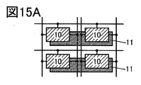
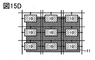
図15A乃至図15Dは、画素の構成を説明する図である。
図16は、画素の構成を説明するブロック図である。
図17は、画素の構成を説明するブロック図である。
図18A、図18Bは、回路10を説明する回路図である。
図19A乃至図19Eは、回路10の一部を説明する回路図である。
図20A、図20Bは、回路10を説明する回路図である。
図21A乃至図21Dは、撮像装置の画素の構成を説明する図である。
図22A乃至図22Cは、光電変換デバイスの構成を説明する図である。
図23は、画素を説明する断面図である。
図24A乃至図24Cは、Siトランジスタを説明する図である。
図25は、画素を説明する断面図である。
図26は、画素を説明する断面図である。
図27A乃至図27Dは、OSトランジスタを説明する図である。
図28は、画素を説明する断面図である。
図29は、画素を説明する断面図である。
図30は、画素を説明する断面図である。
図31A乃至図31Cは、画素を説明する斜視図(断面図)である。
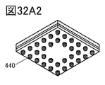
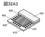
図32A1乃至図32A3、図32B1乃至図32B3は、撮像装置を収めたパッケージ、モジュールの斜視図である。
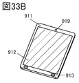
図33A乃至図33Fは、電子機器を説明する図である。
FIG. 1 is a diagram illustrating pixels.
2A and 2B are circuit diagrams illustrating the
FIG. 3 is a circuit diagram illustrating the
FIG. 4 is a timing chart illustrating the operation of the pixels.
FIG. 5 is a diagram illustrating the operation of the
FIG. 6 is a timing chart illustrating the operation of the pixels.
FIG. 7 is a diagram illustrating the operation of the
FIG. 8 is a diagram illustrating the operation of the
FIG. 9 is a timing chart illustrating the operation of the pixels.
FIG. 10 is a diagram illustrating the operation of the
FIG. 11 is a timing chart illustrating the operation of the pixels.
FIG. 12 is a diagram illustrating the operation of the
FIG. 13 is a timing chart illustrating the operation of the pixels.
FIG. 14 is a block diagram illustrating an imaging device.
15A to 15D are diagrams for explaining the configuration of pixels.
FIG. 16 is a block diagram illustrating a pixel configuration.
FIG. 17 is a block diagram illustrating a pixel configuration.
18A and 18B are circuit diagrams illustrating the
19A to 19E are circuit diagrams illustrating a part of the
20A and 20B are circuit diagrams illustrating the
21A to 21D are diagrams for explaining the configuration of pixels of the image pickup apparatus.
22A to 22C are diagrams for explaining the configuration of the photoelectric conversion device.
FIG. 23 is a cross-sectional view illustrating the pixels.
24A to 24C are diagrams for explaining Si transistors.
FIG. 25 is a cross-sectional view illustrating the pixels.
FIG. 26 is a cross-sectional view illustrating the pixels.
27A to 27D are diagrams illustrating an OS transistor.
FIG. 28 is a cross-sectional view illustrating the pixels.
FIG. 29 is a cross-sectional view illustrating the pixels.
FIG. 30 is a cross-sectional view illustrating the pixels.
31A to 31C are perspective views (cross-sectional views) illustrating pixels.
32A1 to 32A3 and 32B1 to 32B3 are perspective views of a package and a module containing an imaging device.
33A to 33F are diagrams for explaining an electronic device.
実施の形態について、図面を用いて詳細に説明する。但し、本発明は以下の説明に限定されず、本発明の趣旨およびその範囲から逸脱することなくその形態および詳細を様々に変更し得ることは当業者であれば容易に理解される。したがって、本発明は以下に示す実施の形態の記載内容に限定して解釈されるものではない。なお、以下に説明する発明の構成において、同一部分または同様な機能を有する部分には同一の符号を異なる図面間で共通して用い、その繰り返しの説明は省略することがある。なお、図を構成する同じ要素のハッチングを異なる図面間で適宜省略または変更する場合もある。 The embodiment will be described in detail with reference to the drawings. However, the present invention is not limited to the following description, and it is easily understood by those skilled in the art that the form and details thereof can be variously changed without departing from the spirit and scope of the present invention. Therefore, the present invention is not construed as being limited to the description of the embodiments shown below. In the configuration of the invention described below, the same reference numerals may be used in common between different drawings for the same parts or parts having similar functions, and the repeated description thereof may be omitted. The hatching of the same element constituting the drawing may be omitted or changed as appropriate between different drawings.
また、回路図上では単一の要素として図示されている場合であっても、機能的に不都合がなければ、当該要素が複数で構成されてもよい。例えば、スイッチとして動作するトランジスタは、複数が直列または並列に接続されてもよい場合がある。また、キャパシタを分割して複数の位置に配置する場合もある。 Further, even if the element is shown as a single element on the circuit diagram, the element may be composed of a plurality of elements as long as there is no functional inconvenience. For example, a plurality of transistors operating as switches may be connected in series or in parallel. In addition, the capacitor may be divided and arranged at a plurality of positions.
また、一つの導電体が、配線、電極および端子のような複数の機能を併せ持っている場合があり、本明細書においては、同一の要素に対して複数の呼称を用いる場合がある。また、回路図上で要素間が直接接続されているように図示されている場合であっても、実際には当該要素間が一つまたは複数の導電体を介して接続されている場合があり、本明細書ではこのような構成でも直接接続の範疇に含める。 In addition, one conductor may have a plurality of functions such as wiring, electrodes, and terminals, and in the present specification, a plurality of names may be used for the same element. Further, even if the elements are shown to be directly connected on the circuit diagram, the elements may actually be connected via one or a plurality of conductors. , In the present specification, such a configuration is also included in the category of direct connection.
(実施の形態1)
本実施の形態では、本発明の一態様である撮像装置について、図面を参照して説明する。
(Embodiment 1)
In the present embodiment, the image pickup apparatus according to one aspect of the present invention will be described with reference to the drawings.
本発明の一態様は、フレーム間でデータを比較し、その結果に従って読み出しを行うか否かを判定する機能を有する。読み出しを行うか否かは、画素単位で制御することができる。 One aspect of the present invention has a function of comparing data between frames and determining whether or not to perform reading according to the result. Whether or not to read can be controlled on a pixel-by-pixel basis.
画素には、第1の回路および第2の回路が設けられる。第1の回路は撮像データを生成することができ、初期フレームのデータとの差である差分データを保持することができる。第2の回路には、当該差分データと任意に設定する電圧範囲を比較する回路が設けられる。第2の回路は、その比較結果に従った読み出し信号を第1の回路に供給する。 The pixel is provided with a first circuit and a second circuit. The first circuit can generate imaging data and can hold difference data which is a difference from the data of the initial frame. The second circuit is provided with a circuit for comparing the difference data with a voltage range arbitrarily set. The second circuit supplies a read signal according to the comparison result to the first circuit.
当該構成を用いることで、例えば、当該差分データが設定した電圧範囲内にあると判定された場合は画素から読み出しを行わず、電圧範囲内にないと判定された場合に画素から読み出しを行うことができる。 By using this configuration, for example, when it is determined that the difference data is within the set voltage range, the reading is not performed from the pixel, and when it is determined that the difference data is not within the voltage range, the reading is performed from the pixel. Can be done.
したがって、初期フレームのデータと同一とみなせるデータが取得された場合は読み出し動作を省略することができ、消費電力を低減させることができる。なお、当該動作を行う場合は、初期フレームのデータをベースに、読み出しを行った画素のデータのみを書き換えてフレームデータを生成すればよい。 Therefore, when data that can be regarded as the same as the data of the initial frame is acquired, the read operation can be omitted, and the power consumption can be reduced. When performing the operation, it is sufficient to rewrite only the data of the read pixel based on the data of the initial frame to generate the frame data.
<画素回路>
図1は、本発明の一態様の撮像装置が有する画素の回路図である。画素は、回路10および回路11を有する。回路10は、撮像データの生成および保持を行う機能を有する。また、第1のフレーム(初期フレーム)の期間で取得したデータと第n(nは2以上の自然数)フレーム(対象フレーム)の期間で取得したデータとの差である差分データも保持することができる。回路11は、判定回路であり、当該差分データの大小を判定し、回路10から読み出しを行うか否かを判定することができる。
<Pixel circuit>
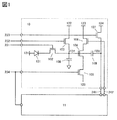
FIG. 1 is a circuit diagram of pixels included in the image pickup apparatus according to one aspect of the present invention. The pixel has a
<回路10>
回路10は、光電変換デバイス101と、トランジスタ102と、トランジスタ103と、トランジスタ104と、トランジスタ105と、トランジスタ106と、トランジスタ107と、キャパシタ108と、キャパシタ109を有する。なお、キャパシタ108は省略することもできる。
<
The
光電変換デバイス101の一方の電極は、トランジスタ102のソースまたはドレインの一方と電気的に接続される。トランジスタ102のソースまたはドレインの他方は、トランジスタ103のソースまたはドレインの一方、トランジスタ104のゲート、キャパシタ108の一方の電極およびキャパシタ109の一方の電極と電気的に接続される。トランジスタ104のソースまたはドレインの一方は、トランジスタ105のソースまたはドレインの一方と電気的に接続される。トランジスタ104のソースまたはドレインの他方は、トランジスタ106のソースまたはドレインの一方と電気的に接続される。キャパシタ109の他方の電極は、トランジスタ107のソースまたはドレインの一方と電気的に接続される。
One electrode of the
また、トランジスタ106のゲートは、配線242を介して回路11と電気的に接続される。キャパシタ109の他方の電極は、配線241を介して回路11と電気的に接続される。
Further, the gate of the
ここで、トランジスタ102のソースまたはドレインの他方、トランジスタ103のソースまたはドレインの一方、トランジスタ104のゲート、キャパシタ108の一方の電極およびキャパシタ109の一方の電極が接続される点(配線)をノードFD1とする。また、キャパシタ109の他方の電極、トランジスタ107のソースまたはドレインの一方および配線241が接続する点(配線)をノードFD2とする。ノードFD1は、各フレーム期間で取得したデータを保持することができる。ノードFD2は、初期フレームのデータまたは、初期フレームのデータと対象フレームのデータとの差である差分データを保持することができる。
Here, the node FD1 is a point (wiring) to which the source or drain of the
光電変換デバイス101の他方の電極は、配線121と電気的に接続される。トランジスタ103のソースまたはドレインの他方は、配線122と電気的に接続される。トランジスタ105のソースまたはドレインの他方は、配線125と電気的に接続される。トランジスタ106のソースまたはドレインの他方は、配線123と電気的に接続される。トランジスタ107のソースまたはドレインの他方は、配線124と電気的に接続される。
The other electrode of the
トランジスタ102のゲートは、配線231と電気的に接続される。トランジスタ103のゲートは、配線232と電気的に接続される。トランジスタ105のゲートは、配線234と電気的に接続される。トランジスタ107のゲートは、配線233と電気的に接続される。なお、配線234は、回路11とも電気的に接続される。
The gate of the
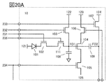
配線121乃至124は、電源線としての機能を有することができる。例えば、配線121は低電位電源線、配線122、123、124は高電位電源線とすることができる。なお、図1に示す構成では光電変換デバイス101のカソード側がトランジスタ102と電気的に接続する構成であるため、電源線は上記の通りとなる。一方で、図2Aに示すように、光電変換デバイス101のアノード側がトランジスタ102と電気的に接続する構成としてもよい。この場合は、配線122を低電位電源線、配線121、123、124を高電位電源線とすればよい。
Wiring 121 to 124 can have a function as a power supply line. For example, the
配線231乃至234は、各トランジスタの導通を制御する信号線としての機能を有することができる。配線125は出力線としての機能を有することができ、例えば、層間二重サンプリング回路(CDS回路)、A/D変換回路などを有する読み出し回路と電気的に接続される。
The
トランジスタ102は、ノードFD1の電位を制御する機能を有する。トランジスタ103は、ノードFD1の電位をリセットする機能を有する。トランジスタ104は、ソースフォロア回路の要素として機能する。トランジスタ105およびトランジスタ106は、画素の出力を選択する機能を有する。トランジスタ107は、ノードFD2の電位をリセットする機能を有する。
The
回路10が有するトランジスタには、チャネル形成領域に金属酸化物を有するトランジスタ(以下、OSトランジスタ)を用いることが好ましい。OSトランジスタは、オフ電流が極めて低い特性を有する。特に、トランジスタ102、103、107にオフ電流の低いトランジスタを用いることが好ましい。これらのトランジスタをOSトランジスタとすることで、ノードFD1およびノードFD2で電荷を保持できる期間を極めて長くすることができ、劣化の少ない画像データを読み出すことができる。
As the transistor included in the
また、トランジスタ102乃至107には、チャネル形成領域にシリコンを有するトランジスタ(以下、Siトランジスタ)を用いることもできる。Siトランジスタとしては、アモルファスシリコンを有するトランジスタ、結晶性のシリコン(微結晶シリコン、低温ポリシリコン、単結晶シリコン)を有するトランジスタなどが挙げられる。Siトランジスタは移動度が高く、高速動作に適している。
Further, as the
なお、トランジスタ102、103がSiトランジスタである場合は、図2Bに示すように、さらにトランジスタ111を設けた構成とすることが好ましい。ここで、トランジスタ111はOSトランジスタである。
When the
トランジスタ111のソースまたはドレインの一方は、トランジスタ102のソースまたはドレインの他方、およびトランジスタ103のソースまたはドレインの一方と電気的に接続される。トランジスタ111のソースまたはドレインの他方は、トランジスタ104のゲート、キャパシタ108の一方の電極およびキャパシタ109の一方の電極と電気的に接続される。
One of the source or drain of the
トランジスタ111のゲートは、配線235と電気的に接続される。配線235は、トランジスタ111の導通を制御する信号線としての機能を有することができる。
The gate of the
図2Bの構成では、トランジスタ111のソースまたはドレインの他方、トランジスタ104のゲート、キャパシタ108の一方の電極およびキャパシタ109の一方の電極が接続される点(配線)がノードFD1となる。
In the configuration of FIG. 2B, the node FD1 is a point (wiring) to which the source or drain of the
トランジスタ111がオフ電流の低いOSトランジスタであるため、ノードFD1およびノードFD2の電荷の保持機能を高めることができる。また、光電変換デバイス101をシリコン基板に形成する埋め込みフォトダイオードとすることができるため、ノイズの少ない画素回路を形成することができる。
Since the
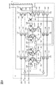
<回路11>
図3に回路11の回路図を示す。回路11は、比較回路としてセンスアンプ11Aおよびセンスアンプ11Bを有する。また、出力回路11Cを有する。また、センスアンプ11A、11Bおよび出力回路11Cに接続する信号線の一部にはインバータ171、172が接続されている。なお、回路11を構成する各要素の接続関係は図3を参照し、詳細な説明は省略する。
<
FIG. 3 shows a circuit diagram of the
センスアンプ11Aは、高電位電源線(配線127)と接続する電源スイッチ(トランジスタ131、133)にインバータラッチ回路(トランジスタ141、142、143、144)が電気的に接続され、インバータラッチ回路がトランジスタ145およびトランジスタ146を介して低電位電源線(配線128)と接続する電源スイッチ(トランジスタ135、137)と電気的に接続する構成を有している。
In the
トランジスタ145のゲートは、配線241を介して回路10のノードFD2と電気的に接続される。トランジスタ146のゲートは、配線238と電気的に接続される。配線238は、目的によって定められた定電位が供給される配線である。
The gate of the
また、インバータラッチ回路のノードLATNBにはトランジスタ147が電気的に接続され、ノードLATNにはトランジスタ148が電気的に接続される。トランジスタ147はノードLATNBを配線129の電位にプリチャージする機能を有する。トランジスタ148は、ノードLATNを配線129の電位にプリチャージする機能を有する。配線129の電位は、例えば、配線127の電位と配線128の電位の中間程度の電位とすることができる。
Further, the
センスアンプ11Bは、高電位電源線(配線127)と接続する電源スイッチ(トランジスタ132、134)にインバータラッチ回路(トランジスタ151、152、153、154)が電気的に接続され、インバータラッチ回路がトランジスタ155およびトランジスタ156を介して低電位電源線(配線128)と接続する電源スイッチ(トランジスタ136、138)と電気的に接続する構成を有している。
In the
トランジスタ155のゲートは、配線241を介して回路10のノードFD2と電気的に接続される。トランジスタ156のゲートは、配線239と電気的に接続される。配線239は、目的によって定められた定電位が供給される配線である。
The gate of the
また、インバータラッチ回路のノードLATPBにはトランジスタ157が電気的に接続され、ノードLATPにはトランジスタ158が電気的に接続される。トランジスタ157は、ノードLATPBを配線129の電位にプリチャージする機能を有する。トランジスタ158は、ノードLATPを配線129の電位にプリチャージする機能を有する。
Further, the
出力回路11Cは、高電位電源線(配線127)と接続する電源スイッチ(トランジスタ161、162)、低電位電源線(配線128)と接続する電源スイッチ(トランジスタ167、168)、およびトランジスタ163、164、165、166、169を有する。それぞれのトランジスタは、出力ノードPCTRと電気的に接続される。
The output circuit 11C includes a power switch (
また、トランジスタ164、165のゲートは、ノードLATNと電気的に接続される。トランジスタ163、166のゲートは、ノードLATPBと電気的に接続される。トランジスタ169のゲートは、インバータ172を介して配線236と電気的に接続される。出力ノードPCTRは、配線242を介して回路10が有するトランジスタ106のゲートと電気的に接続される。
Further, the gates of the
回路11には、配線236、234、237が電気的に接続される。配線236、234、237は、トランジスタの導通を制御するための信号線である。
配線236に高電位(“H”)が供給されると、ノードPCTRの電位が強制的に高電位(“H”)となり、回路10のトランジスタ106が導通する。すなわち、回路10が有する二つの選択トランジスタのうちの一つであるトランジスタ106を強制的に導通することができる。
When a high potential (“H”) is supplied to the
配線236は、トランジスタ131、131、161のゲートと電気的に接続することができる。また、配線236は、インバータ172を介して、トランジスタ135、136、167、169のゲートと電気的に接続することができる。
Wiring 236 can be electrically connected to the gates of
配線234は、インバータ171を介して、トランジスタ133、134、162のゲートと電気的に接続することができる。また、配線234は、トランジスタ137、138、168のゲートと電気的に接続することができる。配線236に低電位(“L”)が供給され、かつ配線234に高電位(“H”)が供給されると、各電源スイッチをオン状態とすることができる。
The
配線237は、トランジスタ147、148、157、158のゲートと電気的に接続することができる。配線237に高電位(“H”)が供給されると、トランジスタ147、148、157、158が導通し、ノードLATNB、ノードLATN、ノードLATPB、ノードLATPのプリチャージを行うことができる。
Wiring 237 can be electrically connected to the gates of
回路11は、pチャネル型トランジスタ(トランジスタ131、132、133、134、141、143、151、153、161、162、164、169)を有する。また、nチャネル型トランジスタ(トランジスタ135、136、137、138、142、144、145、146、147、148、152、154、155、156、157、158、165、166、167、168)を有する。
The
これらのトランジスタとしては、Siトランジスタを用いることが好ましい。または、nチャネル型トランジスタにOSトランジスタを用いてもよい。特に電源スイッチを構成するトランジスタ135、136、137、138にOSトランジスタを用いることで、非動作時に生じる電源線間の不要なリーク電流を抑えることができ、電力消費を抑えることができる。
As these transistors, it is preferable to use Si transistors. Alternatively, an OS transistor may be used as the n-channel transistor. In particular, by using OS transistors for the
<回路10および回路11の動作>
次に回路10および回路11の動作について説明する。動作には、初期フレームの撮像動作および読み出し動作、通常撮像動作、差分計算動作、判定動作などがあり、順に説明する。なお、以下の説明において、nチャネル型トランジスタを導通させる高電位信号およびpチャネル型トランジスタを非導通にする高電位信号を“H”、nチャネル型トランジスタを非導通にする低電位信号およびpチャネル型トランジスタを導通させる低電位信号を“L”で表す。
<Operation of
Next, the operation of the
また、回路11において、配線238には電位VN、配線239には電位VPが供給されていることとする。電位VNは判定に用いる電圧範囲の下端の電圧、電位VPは上端の電圧である。当該電圧範囲は、初期フレームのデータと対象フレームのデータを同じとみなす範囲に相当する。
Further, in the
<初期フレームの撮像動作>
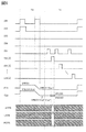
図4は、初期フレームの撮像動作(期間T1)、読み出し動作(期間T2)を説明するタイミングチャートである。なお、図中の[0]乃至[n](nは自然数)は、行番号を表している。また、以下の説明においては、行番号[0]に関してのみ説明を行う。
<Initial frame imaging operation>
FIG. 4 is a timing chart for explaining the imaging operation (period T1) and the reading operation (period T2) of the initial frame. Note that [0] to [n] (n is a natural number) in the figure represent line numbers. Further, in the following description, only the line number [0] will be described.
期間T1において、配線231の電位を“H”、配線232の電位を“H”、配線233の電位を“H”、配線236の電位を“L”、配線237の電位を“L”、配線234[0:n]の電位を“L”とすると、回路10において、トランジスタ102、103、107が導通し、光電変換デバイス101のカソードおよびノードFD1の電位が配線122の電位“VRES1”にリセットされる。また、ノードFD2の電位が配線124の電位“VRES2”にリセットされる。
In the period T1, the potential of the
次に、配線231の電位を“L”とすると、光電変換デバイス101の動作に応じてカソードに電荷が蓄積する。また、配線232の電位を“L”とし、トランジスタ103を非導通としてノードFD1の電位を“VRES1”に保持する。
Next, assuming that the potential of the
次に、所定の露光時間経過後に配線231の電位を“H”とすると、光電変換デバイス101のカソードに蓄積した電荷がノードFD1に転送される。このとき、ノードFD1の電位は、転送された電荷量に応じた電位(“Vref”)分だけ低下し、“VRES1−Vref”になる。このとき、ノードFD2には“VRES2”が供給されている状態とする。
Next, when the potential of the
次に、配線231の電位を“L”、配線233の電位を“L”とし、トランジスタ102、107を非導通として、ノードFD1の電位を“VRES1−Vref”に保持する。また、ノードFD2の電位を“VRES2”に保持する。ここで、“VRES2”は、初期フレームのデータを置き換えた値であるともいえる。以上が初期フレームの撮像動作の説明である。
Next, the potential of the
<初期フレームの読み出し動作> <Reading operation of initial frame>
期間T2において、配線231の電位を“L”、配線232の電位を“L”、配線233の電位を“L”、配線236の電位を“H”、配線237の電位を“L”、配線234[0:n]の電位を“L”とすると、図5に示すように、回路11において、電源スイッチがすべてオフとなり、トランジスタ169が導通する。したがって、出力ノードPCTRの電位が“H”となり、回路10において、トランジスタ106が導通し、トランジスタ104のソースまたはドレインの他方に配線123の電位(電源電位)が供給される。なお、図中の○はトランジスタの導通、×はトランジスタの非導通を示している。
In the period T2, the potential of the
次に、配線234[0]の電位を“H”とすると、トランジスタ105が導通し、ノードFD1の電位に応じたデータが配線125に出力される。以上が初期フレームの読み出し動作の説明である。ここで読み出されたデータは、例えば、フレームメモリなどに保持することができる。
Next, assuming that the potential of the wiring 234 [0] is “H”, the
<通常撮像動作および差分計算動作>
図6は、初期フレームの読み出し動作(図4の期間T2)につづく通常撮像動作および差分計算動作(期間T3)、差分判定動作および読み出し動作(期間T4)を説明するタイミングチャートである。
<Normal imaging operation and difference calculation operation>
FIG. 6 is a timing chart illustrating a normal imaging operation and a difference calculation operation (period T3), a difference determination operation, and a reading operation (period T4) following the initial frame read operation (period T2 in FIG. 4).
期間T3において、配線231の電位を“H”、配線232の電位を“H”、配線233の電位を“L”、配線236の電位を“L”、配線237の電位を“L”、配線234[0:n]の電位を“L”とすると、トランジスタ102、103が導通し、光電変換デバイス101のカソードおよびノードFD1の電位が配線122の電位“VRES1”にリセットされる。
In the period T3, the potential of the
このとき、ノードFD2はフローティング状態にあるため、キャパシタ109の容量結合により、ノードFD1の電位の変化分がノードFD2の電位に加算される。ノードFD1の電位の変化分は“+Vref”であることから、ノードFD2の電位は、“VRES2+Vref”となる。
At this time, since the node FD2 is in a floating state, the change in the potential of the node FD1 is added to the potential of the node FD2 due to the capacitive coupling of the
次に、配線231の電位を“L”とすると、光電変換デバイス101の動作に応じてカソードに電荷が蓄積する。また、配線232の電位を“L”とし、トランジスタ103を非導通としてノードFD1の電位を“VRES1”に保持する。
Next, assuming that the potential of the
次に、所定の露光時間経過後に配線231の電位を“H”とすると、光電変換デバイス101のカソードに蓄積した電荷がノードFD1に転送される。このとき、ノードFD1の電位は、転送された電荷量に応じた電位(“Vtar1”)だけ低下し、“VRES1−Vtar1”になる。また、キャパシタ109の容量結合により、ノードFD1の電位の変化分がノードFD2の電位に加算される。ノードFD1の電位の変化分は、“−Vtar1”であることからノードFD2の電位は、“VRES2+Vref−Vtar1”となる。
Next, when the potential of the
次に、配線231の電位を“L”とし、トランジスタ102を非導通として、ノードFD1の電位を“VRES1−Vtar1”に保持する。また、ノードFD2の電位を“VRES2+Vref−Vtar1”に保持する。
Next, the potential of the
以上が、通常撮像動作および差分計算動作である。通常撮像動作の結果として、ノードFD1には、“VRES1−Vtar1”が保持される。また、差分計算動作の結果として、ノードFD2に“VRES2+Vref−Vtar1”が保持される。“VRES2”はリセット電位であるが、0とみなすことができる。したがって、“+Vref−Vtar1”は、初期フレームのデータと通常撮像動作で取得したデータとの差分そのものである。 The above is the normal imaging operation and the difference calculation operation. As a result of the normal imaging operation, "VRES1-Vtar1" is held in the node FD1. Further, as a result of the difference calculation operation, "VRES2 + Vref-Vtar1" is held in the node FD2. “VRES2” is the reset potential, but can be regarded as 0. Therefore, "+ Vref-Vtar1" is the difference itself between the data of the initial frame and the data acquired by the normal imaging operation.
<差分判定動作、読み出し動作(差分超過なし)> <Difference judgment operation, read operation (no difference excess)>
期間T4において、配線231の電位を“L”、配線232の電位を“L”、配線233の電位を“L”、配線236の電位を“L”、配線237の電位を“H”、配線234[0:n]の電位を“L”とすると、図7に示すように、回路11において、トランジスタ147、148、157、158が導通し、ノードLATNB、ノードLATN、ノードLATPBおよびノードLATPが配線129の電位にプリチャージされる。
In the period T4, the potential of the
次に、配線237の電位を“L”、配線234[0]の電位を“H”とすると、図8に示すように、すべての電源スイッチがオン状態となり、センスアンプに電流が流れはじめる。ここで、トランジスタ145のゲートおよびトランジスタ155のゲートにはノードFD2の電位“VRES2+Vref−Vtar1”が供給され、配線238には電位“VN”が供給され、配線239には電位“VP”が供給されている。
Next, assuming that the potential of the
このとき、図6に示すように、“VN”<“VRES2+Vref−Vtar1”<“VP”であれば、トランジスタ145のチャネル抵抗がトランジスタ146のチャネル抵抗よりも低いため、ノードLATNBのプリチャージ電位がノードLATNのプリチャージ電位よりも優先的に低下する。したがって、トランジスタ142、143が導通し、配線127、128から電源電圧が供給されてノードLATNBおよびノードLATNの電位が確定する。
At this time, as shown in FIG. 6, if “VN” <“VRES2 + Vref-Vtar1” <“VP”, the channel resistance of the
また、トランジスタ156のチャネル抵抗がトランジスタ155のチャネル抵抗よりも低いため、ノードLATPのプリチャージ電位がノードLATPBよりも優先的に低下する。したがって、トランジスタ151、154が導通し、配線127、128から電源電圧が供給されてノードLATPおよびノードLATPBの電位が確定する。
Further, since the channel resistance of the
このとき、ノードLATNの電位は“H”、ノードLATPBの電位は“H”となるため、トランジスタ165、166が導通し、トランジスタ163、164が非導通となり、出力ノードPCTRの電位は“L”となる。したがって、回路10では、トランジスタ106が導通せず、トランジスタ104に電源が供給されないため、トランジスタ105が導通してもノードFD1のデータは配線125に出力されない。つまり、“VN”<“VRES2+Vref−Vtar1”<“VP”であれば、回路10からデータは出力されないことになる。
At this time, since the potential of the node LATN is “H” and the potential of the node LATPB is “H”, the
ここで、配線125には、ソースフォロアのバイアストランジスタ(図示なし)が接続されているため、トランジスタ104がデータを出力しなければ、配線125の電位は0Vになる。データを読み出す場合は、バイアストランジスタには定常電流が流れる。したがって、読み出し動作を行わなければ当該定常電流分の電力消費を抑えることができる。
Here, since a source follower bias transistor (not shown) is connected to the
<差分判定動作、読み出し動作(プラス差分超過あり)>
図9のタイミングチャートを用いて、設定した電圧範囲よりも高い側に差分が超過した場合を説明する。なお、期間T5は期間T3と同様の通常撮像動作および差分計算動作であるため、説明は省略する。ただし、通常撮像動作によるノードFD1の電位は、“VRES1−Vtar2”(Vtar1>Vtar2)であり、ノードFD2の電位は、“VRES1+Vref−Vtar2”であり、“VP”<“VRES1+Vref−Vtar2”とする。
<Difference judgment operation, read operation (plus difference excess)>
The case where the difference is exceeded on the side higher than the set voltage range will be described with reference to the timing chart of FIG. Since the period T5 is the same normal imaging operation and difference calculation operation as the period T3, the description thereof will be omitted. However, the potential of the node FD1 by the normal imaging operation is "VRES1-Vtar2"(Vtar1> Vtar2), the potential of the node FD2 is "VRES1 + Vref-Vtar2", and "VP"<"VRES1 + Vref-Vtar2". ..
期間T6において、配線231の電位を“L”、配線232の電位を“L”、配線233の電位を“L”、配線236の電位を“L”、配線237の電位を“H”、配線234[0:n]の電位を“L”とすると、図7に示すように、回路11において、トランジスタ147、148、157、158が導通し、ノードLATNB、ノードLATN、ノードLATPBおよびノードLATPが配線129の電位にプリチャージされる。
In the period T6, the potential of the
次に、配線237の電位を“L”、配線234[0]の電位を“H”とすると、図10に示すように、すべての電源スイッチがオン状態となり、センスアンプに電流が流れはじめる。ここで、トランジスタ145のゲートおよびトランジスタ155のゲートにはノードFD2の電位“VRES2+Vref−Vtar2”が供給され、配線238には電位“VN”が供給され、配線239には電位“VP”が供給されている。
Next, assuming that the potential of the
このとき、図9に示すように、“VN”<“VP”<“VRES2+Vref−Vtar2”であれば、トランジスタ145のチャネル抵抗がトランジスタ146のチャネル抵抗よりも低いため、ノードLATNBのプリチャージ電位がノードLATNのプリチャージ電位よりも優先的に低下する。したがって、トランジスタ142、143が導通し、配線127、128から電源電圧が供給されてノードLATNBおよびノードLATNの電位が確定する。
At this time, as shown in FIG. 9, if “VN” <“VP” <“VRES2 + Vref-Vtar2”, the channel resistance of the
また、トランジスタ155のチャネル抵抗がトランジスタ156のチャネル抵抗よりも低いため、ノードLATPBのプリチャージ電位がノードLATPよりも優先的に低下する。したがって、トランジスタ152、153が導通し、配線127、128から電源電圧が供給されてノードLATPBおよびノードLATPの電位が確定する。
Further, since the channel resistance of the
このとき、ノードLATNの電位は“H”、ノードLATPBの電位は“L”となるため、トランジスタ163、165が導通し、トランジスタ164、166が非導通となり、出力ノードPCTRの電位は“H”となる。したがって、回路10では、トランジスタ106が導通し、トランジスタ104に電源が供給されるため、トランジスタ105の導通によってノードFD1のデータが配線125に出力される。つまり、“VN”<“VP”<“VRES2+Vref−Vtar2”であれば、回路10からデータは出力されることになる。
At this time, since the potential of the node LATN is “H” and the potential of the node LATPB is “L”, the
回路10から出力されたデータは、初期フレームの画像データが保存されたフレームメモリにおいて、当該回路10に相当するアドレスに保存される。つまり、読み出された回路10のアドレスのみデータの書き換えが行われる。このような動作により、すべての回路10のデータを書き換える場合に比べて、書き込み電力を低減させることができる。
The data output from the
なお、読み出し動作を行わない場合でも、A/D変換回路で0Vのアナログデータに対応したデジタルデータが生成される。当該デジタルデータが生成された場合は、フレームメモリへの書き込み動作を行わない制御をすればよい。 Even when the read operation is not performed, the A / D conversion circuit generates digital data corresponding to 0 V analog data. When the digital data is generated, it is sufficient to control so that the writing operation to the frame memory is not performed.
<差分判定動作、読み出し動作(マイナス差分超過あり)>
図11のタイミングチャートを用いて、設定した電圧範囲よりも低い側に差分が超過した場合を説明する。なお、期間T7は期間T3と同様の通常撮像動作および差分計算動作であるため、説明は省略する。ただし、通常撮像動作によるノードFD1の電位は、“VRES1−Vtar3”(“Vtar3”>”Vtar1“)であり、ノードFD2の電位は、“VRES1+Vref−Vtar3”であり、“VRES1+Vref−Vtar3”<“VN”<“VP”とする。
<Difference judgment operation, read operation (with negative difference excess)>
The case where the difference is exceeded on the side lower than the set voltage range will be described with reference to the timing chart of FIG. Since the period T7 is the same normal imaging operation and difference calculation operation as the period T3, the description thereof will be omitted. However, the potential of the node FD1 by the normal imaging operation is "VRES1-Vtar3"("Vtar3">"Vtar1"), the potential of the node FD2 is "VRES1 + Vref-Vtar3", and "VRES1 + Vref-Vtar3"<<" Let VN "<" VP ".
期間T8において、配線231の電位を“L”、配線232の電位を“L”、配線233の電位を“L”、配線236の電位を“L”、配線237の電位を“H”、配線234[0:n]の電位を“L”とすると、図7に示すように、回路11において、トランジスタ147、148、157、158が導通し、ノードLATNB、ノードLATN、ノードLATPBおよびノードLATPが配線129の電位にプリチャージされる。
In the period T8, the potential of the
次に、配線237の電位を“L”、配線234[0]の電位を“H”とすると、図12に示すように、すべての電源スイッチがオン状態となり、センスアンプに電流が流れはじめる。ここで、トランジスタ145のゲートおよびトランジスタ155のゲートにはノードFD2の電位“VRES2+Vref−Vtar3”が供給され、配線238には電位“VN”が供給され、配線239には電位“VP”が供給されている。
Next, assuming that the potential of the
このとき、図11に示すように、“VRES2+Vref−Vtar3”<“VN”<“VP”であれば、トランジスタ146のチャネル抵抗がトランジスタ145のチャネル抵抗よりも低いため、ノードLATNのプリチャージ電位がノードLATNBのプリチャージ電位よりも優先的に低下する。したがって、トランジスタ141、144が導通し、配線127、128から電源電圧が供給されてノードLATNおよびノードLATNBの電位が確定する。
At this time, as shown in FIG. 11, if “VRES2 + Vref-Vtar3” <“VN” <“VP”, the channel resistance of the
また、トランジスタ154のチャネル抵抗がトランジスタ155のチャネル抵抗よりも低いため、ノードLATPのプリチャージ電位がノードLATPBよりも優先的に低下する。したがって、トランジスタ151、154が導通し、配線127、128から電源電圧が供給されてノードLATPおよびノードLATPBの電位が確定する。
Further, since the channel resistance of the
このとき、ノードLATNの電位は“L”、ノードLATPBの電位は“H”となるため、トランジスタ164が導通し、トランジスタ163、165が非導通となり、出力ノードPCTRの電位は“H”となる。したがって、回路10では、トランジスタ106が導通し、トランジスタ104に電源が供給されるため、トランジスタ105の導通によってノードFD1のデータが配線125に出力される。つまり、“VRES2+Vref−Vtar3”<“VN”<“VP”であれば、回路10からデータは出力されることになる。
At this time, since the potential of the node LATN is “L” and the potential of the node LATPB is “H”, the
以上の説明の通り、回路11の動作によって、回路10の出力を制御することができる。なお、時間が経過するほど、初期フレームのデータと対象フレームのデータが大きく乖離するため、初期フレームのデータは、一定期間毎または一定フレーム数毎に更新することが好ましい。なお、1フレーム置きに初期フレームのデータを更新してもよい。
As described above, the output of the
また、図4、6、9、11のタイミングチャートでは、図1に示す回路10の動作を示しているが、図2Bの構成の場合は、図13に示すように配線235の電位供給動作を加えればよい。なお、図13は、初期フレームの撮像動作(期間T1)を示しているが、通常撮像動作(期間T3など)も同様である。
Further, the timing charts of FIGS. 4, 6, 9 and 11 show the operation of the
<撮像装置の構成>
図14は、本発明の一態様の撮像装置を説明するブロック図である。当該撮像装置は、マトリクス状に配列された画素(回路10および回路11)を有する画素アレイ21と、画素アレイ21の行を選択する機能を有する回路22(ロードライバ)と、回路10からデータを読み出す機能を有する回路23と、電源電位を供給する回路28を有する。なお、図14では、それぞれの要素を接続する配線数を簡略化している。また、回路22、23、28は複数であってもよい。
<Configuration of imaging device>
FIG. 14 is a block diagram illustrating an imaging device according to an aspect of the present invention. The image pickup apparatus receives data from a
回路23は、回路10の出力データに対して相関二重サンプリング処理を行うための回路24(CDS回路)と、回路24から出力されたアナログデータをデジタルデータに変換する機能を有する回路25(A/D変換回路等)と、データを出力する列を選択する機能を有する回路26(カラムドライバ)などを有することができる。回路10と回路23は、配線125を介して電気的に接続される。
The
ここで、図14では、回路10と回路11が重なる領域を有するように図示している。詳細は後述するが、回路10と回路11をスタック構造とすることで、画素面積を縮小しやすくなり、解像度を高めることができる。また、回路11をSiトランジスタで形成し、その上に回路10をOSトランジスタで形成することで、貼り合わせなどの工程を行わずにスタック構造を形成することができる。
Here, in FIG. 14, it is illustrated so that the
なお、1個の回路10と1個の回路11が重なる構成に限らない。例えば、図15Aに示すように、水平方向(ゲート線が延在する方向)に並ぶ2個の回路10が1個の回路11と重なる構成であってもよい。または、図15Bに示すように、垂直方向(ソース線が延在する方向)に並ぶ2個の回路10が1個の回路11と重なる構成であってもよい。または、図15Cに示すように、水平垂直方向に並ぶ2×2個の回路10が1個の回路11と重なる構成であってもよい。または、図15Dに示すように、水平垂直方向に並ぶ3×3個の回路10が1個の回路11と重なる構成であってもよい。または、1個の回路11と重なる回路10の数は、3×3個より多くてもよい。
The configuration is not limited to the configuration in which one
このように、1個の回路11に対して、複数の回路10が接続される構成では、いずれか1個の回路10の差分データを取得し、その判定に応じて他の回路10も同じ動作を行えばよい。その一例を次に説明する。
In this way, in the configuration in which a plurality of
図16は、3×3個の回路10(回路10[0,0]乃至[2,2])と1個の回路11の接続形態を説明する図である。各行における3本の信号線(配線231、232、233)は、それぞれ電気的に接続されているため、3×3個の回路10では、読み出し動作以外の動作は同時に行われる。各行の選択信号線(配線234[0:2])は、OR回路112を介して回路11と電気的に接続される。したがって、各行の選択動作に応じて回路11を動作させることができる。
FIG. 16 is a diagram illustrating a connection form between 3 × 3 circuits 10 (circuits 10 [0,0] to [2,2]) and one
ここで、回路11には、いずれか1個の回路10のノードFD2が電気的に接続される。図16では、回路10[0,1]のノードFD2と回路11が接続される例を示しているが、その他の回路10のノードFD2と接続されてもよい。また、回路11の出力ノードPCTRは、すべての回路10と電気的に接続される。したがって、1個の回路10のノードFD2の値に応じて、すべての回路10の読み出しを行うか否かを判定する。このような構成では、回路11の数を減らすことができるため、回路11が有するセンスアンプのプリチャージに要する電力などを削減することができる。
Here, the node FD2 of any one of the
図17は、図16の構成にトランジスタ113を追加し、OR回路112を省いた構成である。トランジスタ113は、回路11の出力ノードPCTRと配線242との間に設けられる。図17の構成では、最初に読み出す行にある回路10のノードFD2と回路11を接続する。トランジスタ113のゲートは、当該行の回路10と接続する配線234と接続される。
FIG. 17 is a configuration in which the
最初の行の読み出し動作において、回路11では出力ノードPCTRの電位が確定し、トランジスタ113が導通して各回路10に出力される。次の行の読み出し時にはトランジスタ113が非導通となるため、配線242の電位が保持される。したがって、全ての回路10で同じ動作(読み出す、または読み出さない)を行うことができる。
In the read operation of the first line, the potential of the output node PCTR is fixed in the
このような構成では、最初の行の選択動作で回路11の出力ノードPCTRに生成した電位を保持することができる。したがって、他の行の選択動作で出力ノードPCTRの電位を生成する必要がないため、回路11の動作回数を削減することができ、消費電力を低減させることができる。
In such a configuration, the potential generated in the output node PCTR of the
本発明の一態様においては、図18Aに例示するように、トランジスタにバックゲートを設けた構成としてもよい。図18Aでは、バックゲートがフロントゲートと電気的に接続された構成を示しており、オン電流を高める効果を有する。または、図18Bに示すようにバックゲートに定電位を供給できる構成としてもよい、当該構成では、トランジスタのしきい値電圧を制御することができる。また、一つの回路内に、図18A、図18Bが混在してもよい。また、バックゲートが設けられないトランジスタが設けられていてもよい。 In one aspect of the present invention, as illustrated in FIG. 18A, the transistor may be provided with a back gate. FIG. 18A shows a configuration in which the back gate is electrically connected to the front gate, which has the effect of increasing the on-current. Alternatively, as shown in FIG. 18B, a constant potential may be supplied to the back gate. In this configuration, the threshold voltage of the transistor can be controlled. Further, FIGS. 18A and 18B may be mixed in one circuit. Further, a transistor without a back gate may be provided.
また、回路10において、配線123と配線125に直列に接続されるトランジスタ104、105、106の並び順は、図1に示す構成以外、図19A乃至図19Eに示す構成であってもよい。
Further, in the
また、図2Bに示す回路10の構成においては、図20Aに示すように、トランジスタ103のソースまたはドレインの一方をトランジスタ111のソースまたはドレインの他方、キャパシタ108の一方の電極およびトランジスタ104のゲートと電気的に接続してもよい。また、図20Bに示すように、トランジスタ102のゲートと、トランジスタ111のゲートを配線231と電気的に接続し、配線235を省いてもよい。
Further, in the configuration of the
本実施の形態は、他の実施の形態の記載と適宜組み合わせることができる。 This embodiment can be appropriately combined with the description of other embodiments.
(実施の形態2)
本実施の形態では、本発明の一態様の撮像装置の構造例などについて説明する。
(Embodiment 2)
In the present embodiment, a structural example of the image pickup apparatus according to one aspect of the present invention will be described.
<構造例>
図21Aは、撮像装置の画素の構造の一例を示す図であり、層561および層563の積層構造とすることができる。
<Structural example>
FIG. 21A is a diagram showing an example of the pixel structure of the image pickup apparatus, and can be a laminated structure of
層561は、光電変換デバイス101を有する。光電変換デバイス101は、図22Aに示すように層565aと、層565bを有することができる。なお、場合によって、層を領域と言い換えてもよい。
図22Aに示す光電変換デバイス101はpn接合型フォトダイオードであり、例えば、層565aにp型半導体、層565bにn型半導体を用いることができる。または、層565aにn型半導体、層565bにp型半導体用いてもよい。
The
上記pn接合型フォトダイオードは、代表的には単結晶シリコンを用いて形成することができる。 The pn junction type photodiode can be typically formed by using single crystal silicon.
また、層561が有する光電変換デバイス101は、図22Bに示すように、層566aと、層566bと、層566cと、層566dとの積層としてもよい。図22Bに示す光電変換デバイス101はアバランシェフォトダイオードの一例であり、層566a、層566dは電極に相当し、層566b、566cは光電変換部に相当する。
Further, as shown in FIG. 22B, the
層566aは、低抵抗の金属層などとすることが好ましい。例えば、アルミニウム、チタン、タングステン、タンタル、銀またはそれらの積層を用いることができる。
The
層566dは、可視光に対して高い透光性を有する導電層を用いることが好ましい。例えば、インジウム酸化物、錫酸化物、亜鉛酸化物、インジウム−錫酸化物、ガリウム−亜鉛酸化物、インジウム−ガリウム−亜鉛酸化物、またはグラフェンなどを用いることができる。なお、層566dを省く構成とすることもできる。
As the
光電変換部の層566b、566cは、例えばセレン系材料を光電変換層としたpn接合型フォトダイオードの構成とするができる。層566bとしてはp型半導体であるセレン系材料を用い、層566cとしてはn型半導体であるガリウム酸化物などを用いることが好ましい。
The
セレン系材料を用いた光電変換デバイスは、可視光に対する外部量子効率が高い特性を有する。当該光電変換デバイスでは、アバランシェ増倍を利用することにより、入射される光の量に対する電子の増幅を大きくすることができる。また、セレン系材料は光吸収係数が高いため、光電変換層を薄膜で作製できるなどの生産上の利点を有する。セレン系材料の薄膜は、真空蒸着法またはスパッタ法などを用いて形成することができる。 A photoelectric conversion device using a selenium-based material has a characteristic of high external quantum efficiency with respect to visible light. In the photoelectric conversion device, the amplification of electrons with respect to the amount of incident light can be increased by utilizing the avalanche multiplication. Further, since the selenium-based material has a high light absorption coefficient, it has a production advantage such that the photoelectric conversion layer can be formed of a thin film. A thin film of a selenium-based material can be formed by a vacuum deposition method, a sputtering method, or the like.
セレン系材料としては、単結晶セレンおよび多結晶セレンなどの結晶性セレン、非晶質セレン、銅、インジウム、セレンの化合物(CIS)、または、銅、インジウム、ガリウム、セレンの化合物(CIGS)などを用いることができる。 Examples of the selenium-based material include crystalline selenium such as single crystal selenium and polycrystalline selenium, amorphous selenium, copper, indium, and selenium compounds (CIS), or copper, indium, gallium, and selenium compounds (CIGS). Can be used.
n型半導体は、バンドギャップが広く、可視光に対して透光性を有する材料で形成することが好ましい。例えば、亜鉛酸化物、ガリウム酸化物、インジウム酸化物、錫酸化物、またはそれらが混在した酸化物などを用いることができる。また、これらの材料は正孔注入阻止層としての機能も有し、暗電流を小さくすることもできる。 The n-type semiconductor is preferably formed of a material having a wide bandgap and translucency with respect to visible light. For example, zinc oxide, gallium oxide, indium oxide, tin oxide, or an oxide in which they are mixed can be used. In addition, these materials also have a function as a hole injection blocking layer, and can reduce the dark current.
また、層561が有する光電変換デバイス101は、図22Cに示すように、層567aと、層567bと、層567cと、層567dと、層567eとの積層としてもよい。図22Cに示す光電変換デバイス101は有機光導電膜の一例であり、層567aは下部電極、層567eは透光性を有する上部電極であり、層567b、567c、567dは光電変換部に相当する。
Further, as shown in FIG. 22C, the
光電変換部の層567b、567dのいずれか一方はホール輸送層、他方は電子輸送層とすることができる。また、層567cは光電変換層とすることができる。
One of the
ホール輸送層としては、例えば酸化モリブデンなどを用いることができる。電子輸送層としては、例えば、C60、C70などのフラーレン、またはそれらの誘導体などを用いることができる。 As the hole transport layer, for example, molybdenum oxide or the like can be used. As the electron transport layer, for example, fullerenes such as C 60 and C 70 , or derivatives thereof and the like can be used.
光電変換層としては、n型有機半導体およびp型有機半導体の混合層(バルクヘテロ接合構造)を用いることができる。 As the photoelectric conversion layer, a mixed layer (bulk heterojunction structure) of an n-type organic semiconductor and a p-type organic semiconductor can be used.
図21Aに示す層563としては、例えばシリコン基板を用いることができる。当該シリコン基板は、Siトランジスタ等を有する。当該Siトランジスタを用いて、画素回路を形成することができる。また、画素回路などを駆動する回路、画素回路の読み出し回路、画像処理回路、ニューラルネットワーク、通信回路等を形成することができる。
As the
また、DRAM(Dynamic Random Access Memory)などの記憶回路、CPU(Central Processing Unit)、MCU(Micro Controller Unit)などを形成してもよい。なお、本実施の形態では、実施の形態1で説明した回路10および回路11を画素回路、その他の上記回路を機能回路と呼ぶ。
Further, a storage circuit such as a DRAM (Dynamic Random Access Memory), a CPU (Central Processing Unit), an MCU (Micro Controller Unit), or the like may be formed. In the present embodiment, the
例えば、回路10、回路11および機能回路(回路22、23、28など)が有するトランジスタにおいて、その一部または全てを層563に設けることができる。
For example, in the transistors included in the
また、層563は、図21Bに示すように複数の層の積層であってもよい。図21Bでは、層563a、563b、563cの三層を例示しているが、二層であってもよい。または、層563は四層以上の積層であってもよい。これらの層は、例えば貼り合わせ工程などを用いて積層することができる。当該構成とすることで、画素回路と機能回路を複数の層に分散させ、画素回路と機能回路を重ねて設けることができるため、小型で高機能の撮像装置を作製することができる。
Further, the
また、画素は、図21Cに示すように層561、層562および層563の積層構造を有していてもよい。
Further, as shown in FIG. 21C, the pixel may have a laminated structure of
層562は、OSトランジスタを有することができる。例えば、回路10を層562に形成し、回路11を層563に形成することができる。また、前述した機能回路の一つ以上をOSトランジスタで形成してもよい。または、層563が有するSiトランジスタと層562が有するOSトランジスタを用いて、機能回路の一つ以上を形成してもよい。または、層563をガラス基板などの支持基板とし、層562が有するOSトランジスタで画素回路および機能回路を形成してもよい。
例えば、OSトランジスタおよびSiトランジスタを用いて、ノーマリーオフCPU(「Noff−CPU」ともいう)を実現することができる。なお、Noff−CPUとは、ゲート電圧が0Vであっても非導通状態(オフ状態ともいう)であるノーマリーオフ型のトランジスタを含む集積回路である。 For example, a normally-off CPU (also referred to as "Noff-CPU") can be realized by using an OS transistor and a Si transistor. The Nonf-CPU is an integrated circuit including a normally-off type transistor that is in a non-conducting state (also referred to as an off state) even when the gate voltage is 0V.
Noff−CPUは、Noff−CPU内の動作不要な回路への電力供給を停止し、当該回路を待機状態にすることができる。電力供給が停止され、待機状態になった回路では電力が消費されない。よって、Noff−CPUは、電力使用量を最小限にすることができる。また、Noff−CPUは、電力供給が停止されても設定条件などの動作に必要な情報を長期間保持することができる。待機状態からの復帰は当該回路への電力供給を再開するだけでよく、設定条件などの再書き込みが不要である。すなわち、待機状態からの高速復帰が可能である。このように、Noff−CPUは、動作速度を大きく落とすことなく消費電力を低減できる。 The Noff-CPU can stop the power supply to the unnecessary circuit in the Noff-CPU and put the circuit in the standby state. No power is consumed in the circuit where the power supply is stopped and the circuit is in the standby state. Therefore, the Nonf-CPU can minimize the amount of power used. Further, the Nonf-CPU can retain information necessary for operation such as setting conditions for a long period of time even if the power supply is stopped. To return from the standby state, it is only necessary to restart the power supply to the circuit, and it is not necessary to rewrite the setting conditions and the like. That is, high-speed recovery from the standby state is possible. In this way, the Nonf-CPU can reduce the power consumption without significantly reducing the operating speed.
また、層562は、図21Dに示すように複数の層の積層であってもよい。図21Dでは、層562a、層562bの二層を例示しているが、三層以上の積層であってもよい。これらの層は、例えば層563上に積み上げるように形成することができる。または、層563上に形成した層と、層561上に形成した層とを貼り合わせて形成してもよい。
Further, the
OSトランジスタに用いる半導体材料としては、エネルギーギャップが2eV以上、好ましくは2.5eV以上、より好ましくは3eV以上である金属酸化物を用いることができる。代表的には、インジウムを含む酸化物半導体などであり、例えば、後述するCAAC−OSまたはCAC−OSなどを用いることができる。CAAC−OSは結晶を構成する原子が安定であり、信頼性を重視するトランジスタなどに適する。また、CAC−OSは、高移動度特性を示すため、高速駆動を行うトランジスタなどに適する。 As the semiconductor material used for the OS transistor, a metal oxide having an energy gap of 2 eV or more, preferably 2.5 eV or more, and more preferably 3 eV or more can be used. A typical example is an oxide semiconductor containing indium, and for example, CAAC-OS or CAC-OS, which will be described later, can be used. CAAC-OS is suitable for transistors and the like in which the atoms constituting the crystal are stable and reliability is important. Further, since CAC-OS exhibits high mobility characteristics, it is suitable for a transistor or the like that performs high-speed driving.
OSトランジスタは半導体層のエネルギーギャップが大きいため、数yA/μm(チャネル幅1μmあたりの電流値)という極めて低いオフ電流特性を示す。また、OSトランジスタは、インパクトイオン化、アバランシェ降伏、および短チャネル効果などが生じないなどSiトランジスタとは異なる特徴を有し、高耐圧で信頼性の高い回路を形成することができる。また、Siトランジスタでは問題となる結晶性の不均一性に起因する電気特性のばらつきもOSトランジスタでは生じにくい。 Since the OS transistor has a large energy gap in the semiconductor layer, it exhibits an extremely low off-current characteristic of several yA / μm (current value per 1 μm of channel width). Further, the OS transistor has features different from those of the Si transistor such as impact ionization, avalanche breakdown, and short channel effect, and can form a circuit having high withstand voltage and high reliability. In addition, variations in electrical characteristics due to crystalline non-uniformity, which is a problem with Si transistors, are unlikely to occur with OS transistors.
OSトランジスタが有する半導体層は、例えばインジウム、亜鉛およびM(アルミニウム、チタン、ガリウム、ゲルマニウム、イットリウム、ジルコニウム、ランタン、セリウム、スズ、ネオジムまたはハフニウム等の金属から選ばれた一つ、または複数)を含むIn−M−Zn系酸化物で表記される膜とすることができる。In−M−Zn系酸化物は、例えば、スパッタリング法、ALD(Atomic layer deposition)法、またはMOCVD(Metal organic chemical vapor deposition)法などを用いて形成することができる。 The semiconductor layer of the OS transistor includes, for example, indium, zinc and M (one or more selected from metals such as aluminum, titanium, gallium, germanium, yttrium, zirconium, lanthanum, cerium, tin, neodymium or hafnium). It can be a film represented by an In—M—Zn-based oxide containing. The In-M-Zn-based oxide can be formed by, for example, a sputtering method, an ALD (Atomic layer deposition) method, a MOCVD (metric organic chemical vapor deposition) method, or the like.
In−M−Zn系酸化物をスパッタリング法で成膜する場合、スパッタリングターゲットの金属元素の原子数比は、In≧M、Zn≧Mを満たすことが好ましい。このようなスパッタリングターゲットの金属元素の原子数比として、In:M:Zn=1:1:1、In:M:Zn=1:1:1.2、In:M:Zn=3:1:2、In:M:Zn=4:2:3、In:M:Zn=4:2:4.1、In:M:Zn=5:1:3、In:M:Zn=5:1:6、In:M:Zn=5:1:7、In:M:Zn=5:1:8、In:M:Zn=10:1:3、等が好ましい。なお、成膜される半導体層の原子数比はそれぞれ、上記のスパッタリングターゲットに含まれる金属元素の原子数比のプラスマイナス40%の変動を含む。 When an In—M—Zn-based oxide is formed by a sputtering method, the atomic number ratio of the metal element of the sputtering target preferably satisfies In ≧ M and Zn ≧ M. The atomic number ratio of the metal element of such a sputtering target is In: M: Zn = 1: 1: 1, In: M: Zn = 1: 1: 1.2, In: M: Zn = 3: 1: 1. 2, In: M: Zn = 4: 2: 3, In: M: Zn = 4: 2: 4.1, In: M: Zn = 5: 1: 3, In: M: Zn = 5: 1: 6, In: M: Zn = 5: 1: 7, In: M: Zn = 5: 1: 8, In: M: Zn = 10: 1: 3, and the like are preferable. The atomic number ratio of the semiconductor layer to be formed includes a variation of plus or minus 40% of the atomic number ratio of the metal element contained in the sputtering target.
半導体層としては、キャリア密度の低い酸化物半導体を用いる。例えば、半導体層は、キャリア密度が1×10¹⁷/cm3以下、好ましくは1×1015/cm3以下、さらに好ましくは1×1013/cm3以下、より好ましくは1×1011/cm3以下、さらに好ましくは1×1010/cm3未満であり、1×10−9/cm3以上の酸化物半導体を用いることができる。そのような酸化物半導体を、高純度真性または実質的に高純度真性な酸化物半導体と呼ぶ。当該酸化物半導体は欠陥準位密度が低く、安定な特性を有する酸化物半導体であるといえる。 As the semiconductor layer, an oxide semiconductor having a low carrier density is used. For example, the semiconductor layer has a carrier density of 1 × 10 17 / cm 3 or less, preferably 1 × 10 15 / cm 3 or less, more preferably 1 × 10 13 / cm 3 or less, and more preferably 1 × 10 11 / cm. 3 or less, more preferably less than 1 × 10 10 / cm 3, it is possible to use a 1 × 10 -9 / cm 3 or more oxide semiconductor. Such oxide semiconductors are referred to as high-purity intrinsic or substantially high-purity intrinsic oxide semiconductors. It can be said that the oxide semiconductor is an oxide semiconductor having a low defect level density and stable characteristics.
なお、これらに限られず、必要とするトランジスタの半導体特性および電気特性(電界効果移動度、しきい値電圧等)に応じて適切な組成のものを用いればよい。また、必要とするトランジスタの半導体特性を得るために、半導体層のキャリア密度、不純物濃度、欠陥密度、金属元素と酸素の原子数比、原子間距離、密度等を適切なものとすることが好ましい。 Not limited to these, a transistor having an appropriate composition may be used according to the required semiconductor characteristics and electrical characteristics (field effect mobility, threshold voltage, etc.) of the transistor. Further, in order to obtain the required semiconductor characteristics of the transistor, it is preferable that the carrier density, impurity concentration, defect density, atomic number ratio of metal element and oxygen, interatomic distance, density and the like of the semiconductor layer are appropriate. ..
半導体層を構成する酸化物半導体において、第14族元素の一つであるシリコンまたは炭素が含まれると、酸素欠損が増加し、n型化してしまう。このため、半導体層におけるシリコンまたは炭素の濃度(二次イオン質量分析法により得られる濃度)を、2×10¹⁸atoms/cm3以下、好ましくは2×1017atoms/cm3以下とする。 When silicon or carbon, which is one of the Group 14 elements, is contained in the oxide semiconductor constituting the semiconductor layer, the oxygen deficiency increases and the oxide semiconductor becomes n-type. Therefore, the concentration of silicon or carbon in the semiconductor layer (concentration obtained by secondary ion mass spectrometry) is set to 2 × 10 18 atoms / cm 3 or less, preferably 2 × 10 17 atoms / cm 3 or less.
また、アルカリ金属およびアルカリ土類金属は、酸化物半導体と結合するとキャリアを生成する場合があり、トランジスタのオフ電流が増大してしまうことがある。このため、半導体層におけるアルカリ金属またはアルカリ土類金属の濃度(二次イオン質量分析法により得られる濃度)を、1×10¹⁸atoms/cm3以下、好ましくは2×1016atoms/cm3以下にする。 In addition, alkali metals and alkaline earth metals may generate carriers when combined with oxide semiconductors, which may increase the off-current of the transistor. Therefore, the concentration of alkali metal or alkaline earth metal in the semiconductor layer (concentration obtained by secondary ion mass spectrometry) is 1 × 10 18 atoms / cm 3 or less, preferably 2 × 10 16 atoms / cm 3 or less. To.
また、半導体層を構成する酸化物半導体に窒素が含まれていると、キャリアである電子が生じてキャリア密度が増加し、n型化しやすい。この結果、窒素が含まれている酸化物半導体を用いたトランジスタはノーマリーオン特性となりやすい。このため半導体層における窒素濃度(二次イオン質量分析法により得られる濃度)は、5×10¹⁸atoms/cm3以下にすることが好ましい。 Further, when nitrogen is contained in the oxide semiconductor constituting the semiconductor layer, electrons as carriers are generated, the carrier density is increased, and the n-type is easily formed. As a result, a transistor using an oxide semiconductor containing nitrogen tends to have a normally-on characteristic. Therefore, the nitrogen concentration in the semiconductor layer (concentration obtained by secondary ion mass spectrometry) is preferably 5 × 10 18 atoms / cm 3 or less.
また、半導体層を構成する酸化物半導体に水素が含まれていると、金属原子と結合する酸素と反応して水になるため、酸化物半導体中に酸素欠損を形成する場合がある。酸化物半導体中のチャネル形成領域に酸素欠損が含まれていると、トランジスタはノーマリーオン特性となる場合がある。さらに、酸素欠損に水素が入った欠陥はドナーとして機能し、キャリアである電子が生成されることがある。また、水素の一部が金属原子と結合する酸素と結合して、キャリアである電子を生成する場合がある。したがって、水素が多く含まれている酸化物半導体を用いたトランジスタは、ノーマリーオン特性となりやすい。 Further, when hydrogen is contained in the oxide semiconductor constituting the semiconductor layer, it reacts with oxygen bonded to a metal atom to become water, which may form an oxygen deficiency in the oxide semiconductor. If the channel formation region in the oxide semiconductor contains oxygen deficiency, the transistor may have a normally-on characteristic. In addition, a defect containing hydrogen in an oxygen deficiency may function as a donor and generate electrons as carriers. In addition, a part of hydrogen may be combined with oxygen that is bonded to a metal atom to generate an electron as a carrier. Therefore, a transistor using an oxide semiconductor containing a large amount of hydrogen tends to have a normally-on characteristic.
酸素欠損に水素が入った欠陥は、酸化物半導体のドナーとして機能しうる。しかしながら、当該欠陥を定量的に評価することは困難である。そこで、酸化物半導体においては、ドナー濃度ではなく、キャリア濃度で評価される場合がある。よって、本明細書等では、酸化物半導体のパラメータとして、ドナー濃度ではなく、電界が印加されない状態を想定したキャリア濃度を用いる場合がある。つまり、本明細書等に記載の「キャリア濃度」は、「ドナー濃度」と言い換えることができる場合がある。 Defects containing hydrogen in oxygen deficiencies can function as donors for oxide semiconductors. However, it is difficult to quantitatively evaluate the defect. Therefore, in oxide semiconductors, the carrier concentration may be evaluated instead of the donor concentration. Therefore, in the present specification and the like, as a parameter of the oxide semiconductor, a carrier concentration assuming a state in which an electric field is not applied may be used instead of the donor concentration. That is, the "carrier concentration" described in the present specification and the like may be paraphrased as the "donor concentration".
よって、酸化物半導体中の水素はできる限り低減されていることが好ましい。具体的には、酸化物半導体において、二次イオン質量分析法(SIMS:Secondary Ion Mass Spectrometry)により得られる水素濃度を、1×10²⁰atoms/cm3未満、好ましくは1×1019atoms/cm3未満、より好ましくは5×1018atoms/cm3未満、さらに好ましくは1×1018atoms/cm3未満とする。水素などの不純物が十分に低減された酸化物半導体をトランジスタのチャネル形成領域に用いることで、安定した電気特性を付与することができる。 Therefore, it is preferable that hydrogen in the oxide semiconductor is reduced as much as possible. Specifically, in oxide semiconductors, the hydrogen concentration obtained by secondary ion mass spectrometry (SIMS) is less than 1 × 10 20 atoms / cm 3 , preferably 1 × 10 19 atoms / cm. It is less than 3, more preferably less than 5 × 10 18 atoms / cm 3 , and even more preferably less than 1 × 10 18 atoms / cm 3 . By using an oxide semiconductor in which impurities such as hydrogen are sufficiently reduced in the channel formation region of the transistor, stable electrical characteristics can be imparted.
また、半導体層は、例えば非単結晶構造でもよい。非単結晶構造は、例えば、c軸に配向した結晶を有するCAAC−OS(C−Axis Aligned Crystalline Oxide Semiconductor)、多結晶構造、微結晶構造、または非晶質構造を含む。非単結晶構造において、非晶質構造は最も欠陥準位密度が高く、CAAC−OSは最も欠陥準位密度が低い。 Further, the semiconductor layer may have a non-single crystal structure, for example. The non-single crystal structure includes, for example, a CAAC-OS (C-Axis Aligned Crystalline Oxide Semiconductor) having crystals oriented on the c-axis, a polycrystalline structure, a microcrystal structure, or an amorphous structure. In the non-single crystal structure, the amorphous structure has the highest defect level density, and CAAC-OS has the lowest defect level density.
非晶質構造の酸化物半導体膜は、例えば、原子配列が無秩序であり、結晶成分を有さない。または、非晶質構造の酸化物膜は、例えば、完全な非晶質構造であり、結晶部を有さない。 An oxide semiconductor film having an amorphous structure has, for example, a disordered atomic arrangement and no crystal component. Alternatively, the oxide film having an amorphous structure has, for example, a completely amorphous structure and has no crystal portion.
なお、半導体層が、非晶質構造の領域、微結晶構造の領域、多結晶構造の領域、CAAC−OSの領域、単結晶構造の領域のうち、二種以上を有する混合膜であってもよい。混合膜は、例えば上述した領域のうち、いずれか二種以上の領域を含む単層構造、または積層構造を有する場合がある。 Even if the semiconductor layer is a mixed film having two or more of an amorphous structure region, a microcrystal structure region, a polycrystalline structure region, a CAAC-OS region, and a single crystal structure region. Good. The mixed film may have, for example, a single-layer structure or a laminated structure including any two or more of the above-mentioned regions.
以下では、非単結晶の半導体層の一態様であるCAC(Cloud−Aligned Composite)−OSの構成について説明する。 Hereinafter, the configuration of CAC (Cloud-Linked Composite) -OS, which is one aspect of the non-single crystal semiconductor layer, will be described.
CAC−OSとは、例えば、酸化物半導体を構成する元素が、0.5nm以上10nm以下、好ましくは、1nm以上2nm以下、またはその近傍のサイズで偏在した材料の一構成である。なお、以下では、酸化物半導体において、一つあるいはそれ以上の金属元素が偏在し、該金属元素を有する領域が、0.5nm以上10nm以下、好ましくは、1nm以上2nm以下、またはその近傍のサイズで混合した状態をモザイク状、またはパッチ状ともいう。 The CAC-OS is, for example, a composition of a material in which the elements constituting the oxide semiconductor are unevenly distributed in a size of 0.5 nm or more and 10 nm or less, preferably 1 nm or more and 2 nm or less, or a size close thereto. In the following, in the oxide semiconductor, one or more metal elements are unevenly distributed, and the region having the metal elements is 0.5 nm or more and 10 nm or less, preferably 1 nm or more and 2 nm or less, or a size in the vicinity thereof. The state of being mixed with is also called a mosaic shape or a patch shape.
なお、酸化物半導体は、少なくともインジウムを含むことが好ましい。特にインジウムおよび亜鉛を含むことが好ましい。また、それらに加えて、アルミニウム、ガリウム、イットリウム、銅、バナジウム、ベリリウム、ホウ素、シリコン、チタン、鉄、ニッケル、ゲルマニウム、ジルコニウム、モリブデン、ランタン、セリウム、ネオジム、ハフニウム、タンタル、タングステン、またはマグネシウムなどから選ばれた一種、または複数種が含まれていてもよい。 The oxide semiconductor preferably contains at least indium. In particular, it preferably contains indium and zinc. Also, in addition to them, aluminum, gallium, yttrium, copper, vanadium, beryllium, boron, silicon, titanium, iron, nickel, germanium, zirconium, molybdenum, lantern, cerium, neodymium, hafnium, tantalum, tungsten, or magnesium, etc. One or more selected from the above may be included.
例えば、In−Ga−Zn酸化物におけるCAC−OS(CAC−OSの中でもIn−Ga−Zn酸化物を、特にCAC−IGZOと呼称してもよい。)とは、インジウム酸化物(以下、InOX1(X1は0よりも大きい実数)とする。)、またはインジウム亜鉛酸化物(以下、InX2ZnY2OZ2(X2、Y2、およびZ2は0よりも大きい実数)とする。)と、ガリウム酸化物(以下、GaOX3(X3は0よりも大きい実数)とする。)、またはガリウム亜鉛酸化物(以下、GaX4ZnY4OZ4(X4、Y4、およびZ4は0よりも大きい実数)とする。)などと、に材料が分離することでモザイク状となり、モザイク状のInOX1、またはInX2ZnY2OZ2が、膜中に均一に分布した構成(以下、クラウド状ともいう。)である。 For example, CAC-OS in In-Ga-Zn oxide (In-Ga-Zn oxide may be particularly referred to as CAC-IGZO in CAC-OS) is indium oxide (hereinafter, InO). X1 (X1 is a real number greater than 0), or indium zinc oxide (hereinafter, In X2 Zn Y2 O Z2 (X2, Y2, and Z2 are real numbers greater than 0)) and gallium. With oxide (hereinafter, GaO X3 (X3 is a real number larger than 0)) or gallium zinc oxide (hereinafter, Ga X4 Zn Y4 O Z4 (X4, Y4, and Z4 are real numbers larger than 0)) The material is separated into a mosaic-like structure, and the mosaic-like InO X1 or In X2 Zn Y2 O Z2 is uniformly distributed in the film (hereinafter, also referred to as cloud-like). is there.
つまり、CAC−OSは、GaOX3が主成分である領域と、InX2ZnY2OZ2、またはInOX1が主成分である領域とが、混合している構成を有する複合酸化物半導体である。なお、本明細書において、例えば、第1の領域の元素Mに対するInの原子数比が、第2の領域の元素Mに対するInの原子数比よりも大きいことを、第1の領域は、第2の領域と比較して、Inの濃度が高いとする。
That is, CAC-OS is a composite oxide semiconductor having a structure in which a region containing GaO X3 as a main component and a region containing In X2 Zn Y2 O Z2 or InO X1 as a main component are mixed. In the present specification, for example, the atomic number ratio of In to the element M in the first region is larger than the atomic number ratio of In to the element M in the second region. It is assumed that the concentration of In is higher than that of
なお、IGZOは通称であり、In、Ga、Zn、およびOによる1つの化合物をいう場合がある。代表例として、InGaO3(ZnO)m1(m1は自然数)、またはIn(1+x0)Ga(1−x0)O3(ZnO)m0(−1≦x0≦1、m0は任意数)で表される結晶性の化合物が挙げられる。 In addition, IGZO is a common name, and may refer to one compound consisting of In, Ga, Zn, and O. As a typical example, it is represented by InGaO 3 (ZnO) m1 (m1 is a natural number) or In (1 + x0) Ga (1-x0) O 3 (ZnO) m0 (-1 ≦ x0 ≦ 1, m0 is an arbitrary number). Crystalline compounds can be mentioned.
上記結晶性の化合物は、単結晶構造、多結晶構造、またはCAAC構造を有する。なお、CAAC構造とは、複数のIGZOのナノ結晶がc軸配向を有し、かつa−b面においては配向せずに連結した結晶構造である。 The crystalline compound has a single crystal structure, a polycrystalline structure, or a CAAC structure. The CAAC structure is a crystal structure in which a plurality of IGZO nanocrystals have a c-axis orientation and are connected without being oriented on the ab plane.
一方、CAC−OSは、酸化物半導体の材料構成に関する。CAC−OSとは、In、Ga、Zn、およびOを含む材料構成において、一部にGaを主成分とするナノ粒子状に観察される領域と、一部にInを主成分とするナノ粒子状に観察される領域とが、それぞれモザイク状にランダムに分散している構成をいう。したがって、CAC−OSにおいて、結晶構造は副次的な要素である。 On the other hand, CAC-OS relates to the material composition of oxide semiconductors. CAC-OS is a region that is partially observed as nanoparticles containing Ga as a main component and nanoparticles containing In as a main component in a material composition containing In, Ga, Zn, and O. The regions observed in a shape refer to a configuration in which the regions are randomly dispersed in a mosaic shape. Therefore, in CAC-OS, the crystal structure is a secondary element.
なお、CAC−OSは、組成の異なる二種類以上の膜の積層構造は含まないものとする。例えば、Inを主成分とする膜と、Gaを主成分とする膜との2層からなる構造は、含まない。 The CAC-OS does not include a laminated structure of two or more types of films having different compositions. For example, it does not include a structure consisting of two layers, a film containing In as a main component and a film containing Ga as a main component.
なお、GaOX3が主成分である領域と、InX2ZnY2OZ2、またはInOX1が主成分である領域とは、明確な境界が観察できない場合がある。 In some cases, a clear boundary cannot be observed between the region containing GaO X3 as the main component and the region containing In X2 Zn Y2 O Z2 or InO X1 as the main component.
なお、ガリウムの代わりに、アルミニウム、イットリウム、銅、バナジウム、ベリリウム、ホウ素、シリコン、チタン、鉄、ニッケル、ゲルマニウム、ジルコニウム、モリブデン、ランタン、セリウム、ネオジム、ハフニウム、タンタル、タングステン、またはマグネシウムなどから選ばれた一種、または複数種が含まれている場合、CAC−OSは、一部に該金属元素を主成分とするナノ粒子状に観察される領域と、一部にInを主成分とするナノ粒子状に観察される領域とが、それぞれモザイク状にランダムに分散している構成をいう。 Instead of gallium, select from aluminum, ittrium, copper, vanadium, beryllium, boron, silicon, titanium, iron, nickel, germanium, zirconium, molybdenum, lanthanum, cerium, neodymium, hafnium, tantalum, tungsten, or magnesium. When one or more of these are contained, CAC-OS has a region observed in the form of nanoparticles containing the metal element as a main component and a nano having In as a main component. The regions observed in the form of particles refer to a configuration in which the regions are randomly dispersed in a mosaic pattern.
CAC−OSは、例えば基板を意図的に加熱しない条件で、スパッタリング法により形成することができる。また、CAC−OSをスパッタリング法で形成する場合、成膜ガスとして、不活性ガス(代表的にはアルゴン)、酸素ガス、および窒素ガスの中から選ばれたいずれか一つまたは複数を用いればよい。また、成膜時の成膜ガスの総流量に対する酸素ガスの流量比は低いほど好ましく、例えば酸素ガスの流量比を0%以上30%未満、好ましくは0%以上10%以下とすることが好ましい。 The CAC-OS can be formed by a sputtering method, for example, under the condition that the substrate is not intentionally heated. When CAC-OS is formed by a sputtering method, one or more selected from an inert gas (typically argon), an oxygen gas, and a nitrogen gas may be used as the film forming gas. Good. Further, the lower the flow rate ratio of the oxygen gas to the total flow rate of the film-forming gas at the time of film formation is preferable. For example, the flow rate ratio of the oxygen gas is preferably 0% or more and less than 30%, preferably 0% or more and 10% or less. ..
CAC−OSは、X線回折(XRD:X−ray diffraction)測定法のひとつであるOut−of−plane法によるθ/2θスキャンを用いて測定したときに、明確なピークが観察されないという特徴を有する。すなわち、X線回折測定から、測定領域のa−b面方向、およびc軸方向の配向は見られないことが分かる。 CAC-OS is characterized by the fact that no clear peak is observed when measured using the θ / 2θ scan by the Out-of-plane method, which is one of the X-ray diffraction (XRD) measurement methods. Have. That is, from the X-ray diffraction measurement, it can be seen that the orientation of the measurement region in the ab plane direction and the c-axis direction is not observed.
また、CAC−OSは、プローブ径が1nmの電子線(ナノビーム電子線ともいう。)を照射することで得られる電子線回折パターンにおいて、リング状に輝度の高い領域(リング領域)と、該リング領域に複数の輝点が観測される。したがって、電子線回折パターンから、CAC−OSの結晶構造が、平面方向、および断面方向において、配向性を有さないnc(nano−crystal)構造を有することがわかる。 Further, CAC-OS has a ring-shaped high-brightness region (ring region) and the ring in an electron diffraction pattern obtained by irradiating an electron beam (also referred to as a nanobeam electron beam) having a probe diameter of 1 nm. Multiple bright spots are observed in the area. Therefore, from the electron diffraction pattern, it can be seen that the crystal structure of CAC-OS has an nc (nano-crystal) structure having no orientation in the planar direction and the cross-sectional direction.
また、例えば、In−Ga−Zn酸化物におけるCAC−OSでは、エネルギー分散型X線分光法(EDX:Energy Dispersive X−ray spectroscopy)を用いて取得したEDXマッピングにより、GaOX3が主成分である領域と、InX2ZnY2OZ2、またはInOX1が主成分である領域とが、偏在し、混合している構造を有することが確認できる。 Further, for example, in CAC-OS in In-Ga-Zn oxide, GaO X3 is the main component by EDX mapping obtained by using energy dispersive X-ray spectroscopy (EDX). It can be confirmed that the region and the region containing In X2 Zn Y2 O Z2 or InO X1 as the main component have a structure in which they are unevenly distributed and mixed.
CAC−OSは、金属元素が均一に分布したIGZO化合物とは異なる構造であり、IGZO化合物と異なる性質を有する。つまり、CAC−OSは、GaOX3などが主成分である領域と、InX2ZnY2OZ2、またはInOX1が主成分である領域と、に互いに相分離し、各元素を主成分とする領域がモザイク状である構造を有する。 CAC-OS has a structure different from that of the IGZO compound in which metal elements are uniformly distributed, and has properties different from those of the IGZO compound. That is, the CAC-OS is a region in which GaO X3 or the like is the main component and a region in which In X2 Zn Y2 O Z2 or InO X1 is the main component are phase-separated from each other and each element is the main component. Has a mosaic-like structure.
ここで、InX2ZnY2OZ2、またはInOX1が主成分である領域は、GaOX3などが主成分である領域と比較して、導電性が高い領域である。つまり、InX2ZnY2OZ2、またはInOX1が主成分である領域を、キャリアが流れることにより、酸化物半導体としての導電性が発現する。したがって、InX2ZnY2OZ2、またはInOX1が主成分である領域が、酸化物半導体中にクラウド状に分布することで、高い電界効果移動度(μ)が実現できる。 Here, the region in which In X2 Zn Y2 O Z2 or InO X1 is the main component is a region having higher conductivity than the region in which GaO X3 or the like is the main component. That is, when the carrier flows through the region where In X2 Zn Y2 O Z2 or InO X1 is the main component, the conductivity as an oxide semiconductor is exhibited. Therefore, a high field effect mobility (μ) can be realized by distributing the region containing In X2 Zn Y2 O Z2 or InO X1 as the main component in the oxide semiconductor in a cloud shape.
一方、GaOX3などが主成分である領域は、InX2ZnY2OZ2、またはInOX1が主成分である領域と比較して、絶縁性が高い領域である。つまり、GaOX3などが主成分である領域が、酸化物半導体中に分布することで、リーク電流を抑制し、良好なスイッチング動作を実現できる。 On the other hand, the region in which GaO X3 or the like is the main component is a region having higher insulating property than the region in which In X2 Zn Y2 O Z2 or InO X1 is the main component. That is, since the region containing GaO X3 or the like as the main component is distributed in the oxide semiconductor, the leakage current can be suppressed and a good switching operation can be realized.
したがって、CAC−OSを半導体素子に用いた場合、GaOX3などに起因する絶縁性と、InX2ZnY2OZ2、またはInOX1に起因する導電性とが、相補的に作用することにより、高いオン電流(Ion)、および高い電界効果移動度(μ)を実現することができる。 Therefore, when CAC-OS is used for a semiconductor element, the insulation property caused by GaO X3 and the like and the conductivity caused by In X2 Zn Y2 O Z2 or InO X1 act complementarily to be high. On current (I on ) and high field effect mobility (μ) can be achieved.
また、CAC−OSを用いた半導体素子は、信頼性が高い。したがって、CAC−OSは、様々な半導体装置の構成材料として適している。 Further, the semiconductor element using CAC-OS has high reliability. Therefore, CAC-OS is suitable as a constituent material for various semiconductor devices.
<積層構造1>
次に、撮像装置の積層構造について、断面図を用いて説明する。なお、以下に示す絶縁層および導電層などの要素は一例であり、さらに他の要素が含まれていてもよい。または、以下に示す要素の一部が省かれていてもよい。また、以下に示す積層構造は、必要に応じて、貼り合わせ工程、研磨工程などを用いて形成することができる。
<
Next, the laminated structure of the image pickup apparatus will be described with reference to a cross-sectional view. The elements such as the insulating layer and the conductive layer shown below are examples, and other elements may be included. Alternatively, some of the elements shown below may be omitted. In addition, the laminated structure shown below can be formed by using a bonding step, a polishing step, or the like, if necessary.
図23は、層560、561、層563を有し、層563を構成する層563aと層563bの間に貼り合わせ面を有する積層体の断面図の一例である。
FIG. 23 is an example of a cross-sectional view of a laminated
<層563b>
層563bは、シリコン基板610に設けられた回路11の要素を有する。ここでは、回路11の要素の一部として、インバータ172が有するトランジスタ203およびトランジスタ204、およびトランジスタ169を示している。
<
The
層563bには、シリコン基板610、絶縁層611、612、613、614、615、616、617、618が設けられる。また、導電層619が設けられる。絶縁層611は保護膜としての機能を有する。絶縁層612、613、614、615、616、617は、層間絶縁膜および平坦化膜としての機能を有する。絶縁層618および導電層619は、貼り合わせ層としての機能を有する。導電層619は、トランジスタ169と電気的に接続される。
The
保護膜としては、例えば、窒化シリコン膜、酸化シリコン膜、酸化アルミニウム膜などを用いることができる。層間絶縁膜および平坦化膜としては、例えば、酸化シリコン膜などの無機絶縁膜、アクリル樹脂、ポリイミド樹脂などの有機絶縁膜を用いることができる。キャパシタの誘電体層としては、窒化シリコン膜、酸化シリコン膜、酸化アルミニウム膜などを用いることができる。貼り合わせ層に関しては後述する。 As the protective film, for example, a silicon nitride film, a silicon oxide film, an aluminum oxide film, or the like can be used. As the interlayer insulating film and the flattening film, for example, an inorganic insulating film such as a silicon oxide film or an organic insulating film such as an acrylic resin or a polyimide resin can be used. As the dielectric layer of the capacitor, a silicon nitride film, a silicon oxide film, an aluminum oxide film, or the like can be used. The bonding layer will be described later.
なお、デバイス間の電気的な接続に用いられる配線、電極およびプラグとして用いることのできる導電体には、アルミニウム、クロム、銅、銀、金、白金、タンタル、ニッケル、チタン、モリブデン、タングステン、ハフニウム、バナジウム、ニオブ、マンガン、マグネシウム、ジルコニウム、ベリリウム、インジウム、ルテニウム、イリジウム、ストロンチウム、ランタンなどから選ばれた金属元素、または上述した金属元素を成分とする合金か、上述した金属元素を組み合わせた合金等を適宜選択して用いればよい。当該導電体は単層に限らず、異なる材料で構成された複数の層であってもよい。 Conductors that can be used as wiring, electrodes, and plugs for electrical connections between devices include aluminum, chromium, copper, silver, gold, platinum, tantalum, nickel, titanium, molybdenum, tungsten, and hafnium. , Vanadium, niobium, manganese, magnesium, zirconium, beryllium, indium, ruthenium, iridium, strontium, lanthanum, etc. Etc. may be appropriately selected and used. The conductor is not limited to a single layer, and may be a plurality of layers made of different materials.
<層563a>
層563aは、回路10の要素を有する。ここでは、回路10の要素の一部として、トランジスタ102およびトランジスタ106を示している。図23に示す断面図では、両者の電気的な接続は図示されていない。
<
層563aには、シリコン基板632、絶縁層631、633、634、635、637、638が設けられる。また、導電層636、639が設けられる。
The
絶縁層631および導電層639は、貼り合わせ層としての機能を有する。絶縁層634、635、637は、層間絶縁膜および平坦化膜としての機能を有する。絶縁層633は、保護膜としての機能を有する。絶縁層638は、シリコン基板632と導電層639を絶縁する機能を有する。絶縁層638は、他の絶縁層と同様の材料で形成することができる。また、絶縁層638は、絶縁層631と同一の材料で形成されていてもよい。
The insulating
導電層639は、トランジスタ106のゲートおよび導電層619と電気的に接続される。また、導電層636は、配線121(図1参照)と電気的に接続される。
The
図23に示すSiトランジスタはシリコン基板(シリコン基板610、632)にチャネル形成領域を有するフィン型である。チャネル幅方向の断面(図23の層563aに示すA1−A2の断面)を図24Aに示す。なお、Siトランジスタは、図24Bに示すようにプレーナー型であってもよい。
The Si transistor shown in FIG. 23 is a fin type having a channel forming region on a silicon substrate (
または、図24Cに示すように、シリコン薄膜の半導体層545を有するトランジスタであってもよい。半導体層545は、例えば、シリコン基板632上の絶縁層546上に形成された単結晶シリコン(SOI(Silicon on Insulator))とすることができる。
Alternatively, as shown in FIG. 24C, the transistor may have a
<層561>
層561は、光電変換デバイス101を有する。光電変換デバイス101は、層563a上に形成することができる。図23では、光電変換デバイス101として、図22Cに示す有機光導電膜を光電変換層に用いた構成を示している。なお、ここでは、層567aをカソード、層567eをアノードとする。
<Layer 561>
層561には、絶縁層651、652、653、654、および導電層655が設けられる。
The
絶縁層651、653、654は、層間絶縁膜および平坦化膜としての機能を有する。また、絶縁層654は光電変換デバイス101の端部を覆って設けられ、層567eと層567aとの短絡を防止する機能も有する。絶縁層652は、素子分離層としての機能を有する。素子分離層としては、有機絶縁膜などを用いることが好ましい。
The insulating
光電変換デバイス101のカソードに相当する層567aは、層563aが有するトランジスタ102のソースまたはドレインの一方と電気的に接続される。光電変換デバイス101のアノードに相当する層567eは、導電層655を介して、層563aが有する導電層636と電気的に接続される。
The
<層560>
層560は、層561上に形成される。層560は、遮光層671、光学変換層672およびマイクロレンズアレイ673を有する。
<Layer 560>
遮光層671は、隣接する画素への光の流入を抑えることができる。遮光層671には、アルミニウム、タングステンなどの金属層を用いることができる。また、当該金属層と反射防止膜としての機能を有する誘電体膜を積層してもよい。
The light-
光学変換層672には、カラーフィルタを用いることができる。カラーフィルタに(赤)、G(緑)、B(青)、Y(黄)、C(シアン)、M(マゼンタ)などの色を画素別に割り当てることにより、カラー画像を得ることができる。例えば、図31Aの斜視図(断面を含む)に示すように、カラーフィルタ672R(赤)、カラーフィルタ672G(緑)、カラーフィルタ672B(青)をそれぞれ異なる画素に割り当てることができる。
A color filter can be used for the
また、光学変換層672に波長カットフィルタを用いれば、様々な波長領域における画像が得られる撮像装置とすることができる。
Further, if a wavelength cut filter is used for the
例えば、光学変換層672に可視光線の波長以下の光を遮る赤外線フィルタを用いれば、赤外線撮像装置とすることができる。また、光学変換層672に近赤外線の波長以下の光を遮るフィルタを用いれば、遠赤外線撮像装置とすることができる。また、光学変換層672に可視光線の波長以上の光を遮る紫外線フィルタを用いれば、紫外線撮像装置とすることができる。
For example, if an infrared filter that blocks light having a wavelength equal to or lower than that of visible light is used in the
なお、一つの撮像装置内に異なる光学変換層を複数配置してもよい。例えば、図31Bに示すように、カラーフィルタ672R(赤)、カラーフィルタ672G(緑)、カラーフィルタ672B(青)、赤外線フィルタ672IRをそれぞれ異なる画素に割り当てることができる。当該構成では、可視光画像および赤外光画像を同時に取得することができる。
A plurality of different optical conversion layers may be arranged in one image pickup apparatus. For example, as shown in FIG. 31B, the
または、図31Cに示すように、カラーフィルタ672R(赤)、カラーフィルタ672G(緑)、カラーフィルタ672B(青)、紫外線フィルタ672UVをそれぞれ異なる画素に割り当てることができる。当該構成では、可視光画像および紫外光画像を同時に取得することができる。
Alternatively, as shown in FIG. 31C, the
また、光学変換層672にシンチレータを用いれば、X線撮像装置などに用いる放射線の強弱を可視化した画像を得る撮像装置とすることができる。被写体を透過したX線等の放射線がシンチレータに入射されると、フォトルミネッセンス現象により可視光線または紫外光線などの光(蛍光)に変換される。そして、当該光を光電変換デバイス101で検出することにより画像データを取得する。また、放射線検出器などに当該構成の撮像装置を用いてもよい。
Further, if a scintillator is used for the
シンチレータは、X線またはガンマ線などの放射線が照射されると、そのエネルギーを吸収して可視光または紫外光を発する物質を含む。例えば、Gd2O2S:Tb、Gd2O2S:Pr、Gd2O2S:Eu、BaFCl:Eu、NaI、CsI、CaF2、BaF2、CeF3、LiF、LiI、ZnOなどを樹脂またはセラミクスに分散させたものを用いることができる。 A scintillator contains a substance that absorbs its energy and emits visible or ultraviolet light when irradiated with radiation such as X-rays or gamma rays. For example, Gd 2 O 2 S: Tb, Gd 2 O 2 S: Pr, Gd 2 O 2 S: Eu, BaFCl: Eu, NaI, CsI, CaF 2 , BaF 2 , CeF 3 , LiF, LiI, ZnO, etc. Those dispersed in resin or ceramics can be used.
光学変換層672上にはマイクロレンズアレイ673が設けられる。マイクロレンズアレイ673が有する個々のレンズを通る光が直下の光学変換層672を通り、光電変換デバイス101に照射されるようになる。マイクロレンズアレイ673を設けることにより、集光した光を光電変換デバイス101に入射することができるため、効率よく光電変換を行うことができる。マイクロレンズアレイ673は、撮像の対象の波長の光に対して透光性の高い樹脂またはガラスなどで形成することが好ましい。
A
<貼り合わせ>
次に、層563bと層563aの貼り合わせについて説明する。
<Lasting>
Next, the bonding of the
層563bには、絶縁層618および導電層619が設けられる。導電層619は、絶縁層618に埋設された領域を有する。また、絶縁層618および導電層619の表面は、それぞれ高さが一致するように平坦化されている。
The
層563aには、絶縁層631および導電層639が設けられる。導電層639は、絶縁層631に埋設された領域を有する。また、絶縁層631および導電層639の表面は、それぞれ高さが一致するように平坦化されている。
The
ここで、導電層619および導電層639は、主成分が同一の金属元素であることが好ましい。また、絶縁層618および絶縁層631は、同一の成分で構成されていることが好ましい。
Here, it is preferable that the
例えば、導電層619、639には、Cu、Al、Sn、Zn、W、Ag、PtまたはAuなどを用いることができる。接合のしやすさから、好ましくはCu、Al、W、またはAuを用いる。また、絶縁層618、631には、酸化シリコン、酸化窒化シリコン、窒化酸化シリコン、窒化シリコン、窒化チタンなどを用いることができる。
For example, Cu, Al, Sn, Zn, W, Ag, Pt, Au, or the like can be used for the
つまり、導電層619および導電層639のそれぞれに、上記に示す同一の金属材料を用いることが好ましい。また、絶縁層618および絶縁層631のそれぞれに、上記に示す同一の絶縁材料を用いることが好ましい。当該構成とすることで、層563bと層563aの境を接合位置とする、貼り合わせを行うことができる。
That is, it is preferable to use the same metal material shown above for each of the
なお、導電層619および導電層639は複数の層の多層構造であってもよく、その場合は、表層(接合面)が同一の金属材料であればよい。また、絶縁層618および絶縁層631も複数の層の多層構造であってもよく、その場合は、表層(接合面)が同一の絶縁材料であればよい。
The
当該貼り合わせによって、導電層619および導電層639の電気的な接続を得ることができる。また、絶縁層618および絶縁層631の機械的な強度を有する接続を得ることができる。
By the bonding, an electrical connection between the
金属層同士の接合には、表面の酸化膜および不純物の吸着層などをスパッタリング処理などで除去し、清浄化および活性化した表面同士を接触させて接合する表面活性化接合法を用いることができる。または、温度と圧力を併用して表面同士を接合する拡散接合法などを用いることができる。どちらも原子レベルでの結合が起こるため、電気的だけでなく機械的にも優れた接合を得ることができる。 For bonding between metal layers, a surface-activated bonding method can be used in which the oxide film on the surface and the adsorption layer of impurities are removed by sputtering or the like, and the cleaned and activated surfaces are brought into contact with each other for bonding. .. Alternatively, a diffusion bonding method or the like in which surfaces are bonded to each other by using both temperature and pressure can be used. In both cases, bonding at the atomic level occurs, so that excellent bonding can be obtained not only electrically but also mechanically.
また、絶縁層同士の接合には、研磨などによって高い平坦性を得たのち、酸素プラズマ等で親水性処理をした表面同士を接触させて仮接合し、熱処理による脱水で本接合を行う親水性接合法などを用いることができる。親水性接合法も原子レベルでの結合が起こるため、機械的に優れた接合を得ることができる。 Further, in order to bond the insulating layers to each other, after obtaining high flatness by polishing or the like, the surfaces treated with hydrophilicity by oxygen plasma or the like are brought into contact with each other for temporary bonding, and then main bonding is performed by dehydration by heat treatment. A joining method or the like can be used. Since the hydrophilic bonding method also causes bonding at the atomic level, it is possible to obtain mechanically excellent bonding.
層563bと層563aを貼り合わせる場合、それぞれの接合面には絶縁層と金属層が混在するため、例えば、表面活性化接合法および親水性接合法を組み合わせて行えばよい。
When the
例えば、研磨後に表面を清浄化し、金属層の表面に酸化防止処理を行ったのちに親水性処理を行って接合する方法などを用いることができる。また、金属層の表面をAuなどの難酸化性金属とし、親水性処理を行ってもよい。なお、上述した方法以外の接合方法を用いてもよい。 For example, a method can be used in which the surface is cleaned after polishing, the surface of the metal layer is subjected to an antioxidant treatment, and then a hydrophilic treatment is performed to join the metal layer. Further, the surface of the metal layer may be made of a refractory metal such as Au and subjected to hydrophilic treatment. A joining method other than the above-mentioned method may be used.
上記の貼り合わせにより、層563bが有する要素と、層563aが有する要素を電気的に接続することができる。
By the above bonding, the element of the
<積層構造1の変形例>
図25は、図23に示す積層構造の変形例であり、層561が有する光電変換デバイス101の構成、および層563aの一部構成が異なり、層561と層563aとの間にも貼り合わせ面を有する構成である。
<Modification example of
FIG. 25 is a modification of the laminated structure shown in FIG. 23, in which the configuration of the
層561は、光電変換デバイス101、絶縁層661、662、664、665および導電層685、686を有する。
The
光電変換デバイス101は、シリコン基板に形成されたpn接合型のフォトダイオードであり、p型領域に相当する層565bおよびn型領域に相当する層565aを有する。光電変換デバイス101は埋め込み型フォトダイオードであり、層565aの表面側(電流の取り出し側)に設けられた薄いp型の領域(層565bの一部)によって暗電流を抑えノイズを低減させることができる。
The
絶縁層661、導電層685、686は、貼り合わせ層としての機能を有する。絶縁層662は、層間絶縁膜および平坦化膜としての機能を有する。絶縁層664は、素子分離層としての機能を有する。絶縁層665は、キャリアの流出を抑制する機能を有する。
The insulating
シリコン基板には画素を分離する溝が設けられ、絶縁層665はシリコン基板上面および当該溝に設けられる。絶縁層665が設けられることにより、光電変換デバイス101内で発生したキャリアが隣接する画素に流出することを抑えることができる。また、絶縁層665は、迷光の侵入を抑制する機能も有する。したがって、絶縁層665により、混色を抑制することができる。なお、シリコン基板の上面と絶縁層665との間に反射防止膜が設けられていてもよい。
The silicon substrate is provided with a groove for separating pixels, and the insulating
素子分離層は、LOCOS(LOCal Oxidation of Silicon)法を用いて形成することができる。または、STI(Shallow Trench Isolation)法等を用いて形成してもよい。絶縁層665としては、例えば、酸化シリコン、窒化シリコンなどの無機絶縁膜、ポリイミド、アクリルなどの有機絶縁膜を用いることができる。なお、絶縁層665は多層構成であってもよい。なお、素子分離層を設けない構成とすることもできる。
The element separation layer can be formed by using the LOCOS (LOCOxidation of Silicon) method. Alternatively, it may be formed by using an STI (Shallow Trench Isolation) method or the like. As the insulating
光電変換デバイス101の層565a(n型領域、カソードに相当)は、導電層685と電気的に接続される。層565b(p型領域、アノードに相当)は、導電層686と電気的に接続される。導電層685、686は、絶縁層661に埋設された領域を有する。また、絶縁層661および導電層685、686の表面は、それぞれ高さが一致するように平坦化されている。
The
層563aにおいて、絶縁層637上には、絶縁層638が形成される。また、トランジスタ102のソースまたはドレインの一方と電気的に接続される導電層683、および導電層636と電気的に接続される導電層684が形成される。
In
絶縁層638、導電層683、684は、貼り合わせ層としての機能を有する。導電層683、684は、絶縁層638に埋設された領域を有する。また、絶縁層638および導電層683、684の表面は、それぞれ高さが一致するように平坦化されている。
The insulating
ここで、導電層683、684、685、686は、前述した導電層619、639と同様の貼り合わせ層である。また、絶縁層638、661は、前述した絶縁層618、631と同様の貼り合わせ層である。
Here, the
したがって、導電層683と導電層685を貼り合わせることで、光電変換デバイスの層565a(n型領域、カソードに相当)とトランジスタ102のソースまたはドレインの一方を電気的に接続することができる。また、導電層684と導電層686を貼り合わせることで、光電変換デバイスの層565b(p型領域、アノードに相当)と配線121(図1参照)を電気的に接続することができる。また、絶縁層638と絶縁層661を貼り合わせることで、層561と層563aの電気的な接合および機械的な接合を行うことができる。
Therefore, by laminating the
<積層構造2>
図26は、層560、561、562、563を有し、貼り合わせ面を有さない積層体の断面図の一例である。層563には、Siトランジスタが設けられる。層562には、OSトランジスタが設けられる。なお、層563、層561および層560の構成は、図23に示す構成と同一であるため、ここでは説明を省略する。
<
FIG. 26 is an example of a cross-sectional view of a laminated
<層562>
層562は、層563上に形成される。層562は、OSトランジスタを有する。ここでは、回路10の要素の一部として、トランジスタ102およびトランジスタ106を示している。図26に示す断面図では、両者の電気的な接続は図示されていない。
<Layer 562>
層562には、絶縁層621、622、623、624、625、626、628が設けられる。また、導電層627が設けられる。導電層627は、配線121(図1参照)と電気的に接続することができる。
The
絶縁層621は、ブロッキング層としての機能を有する。絶縁層622、623、625、626、628は、層間絶縁膜および平坦化膜としての機能を有する。絶縁層624は、保護膜としての機能を有する。
The insulating
ブロッキング層としては、水素の拡散を防止する機能を有する膜を用いることが好ましい。Siデバイスにおいて、水素はダングリングボンドを終端するために必要とされるが、OSトランジスタの近傍にある水素は、酸化物半導体層中にキャリアを生成する要因の一つとなり、信頼性を低下させる。したがって、Siデバイスが形成される層とOSトランジスタが形成される層との間には、水素のブロッキング膜が設けられることが好ましい。 As the blocking layer, it is preferable to use a film having a function of preventing the diffusion of hydrogen. In Si devices, hydrogen is required to terminate dangling bonds, but hydrogen in the vicinity of the OS transistor becomes one of the factors that generate carriers in the oxide semiconductor layer, which reduces reliability. .. Therefore, it is preferable to provide a hydrogen blocking film between the layer on which the Si device is formed and the layer on which the OS transistor is formed.
当該ブロッキング膜としては、例えば、酸化アルミニウム、酸化窒化アルミニウム、酸化ガリウム、酸化窒化ガリウム、酸化イットリウム、酸化窒化イットリウム、酸化ハフニウム、酸化窒化ハフニウム、イットリア安定化ジルコニア(YSZ)等を用いることができる。 As the blocking film, for example, aluminum oxide, aluminum nitride, gallium oxide, gallium oxide, yttrium oxide, yttrium oxide, hafnium oxide, hafnium oxide, yttria-stabilized zirconia (YSZ) and the like can be used.
トランジスタ106のゲートは、プラグを介してトランジスタ169と電気的に接続される。
The gate of
トランジスタ102のソースまたはドレインの一方は、層561が有する光電変換デバイス101の層567aと電気的に接続される。導電層627は、層561が有する光電変換デバイス101の層567eと電気的に接続される。
One of the source and drain of the
図27AにOSトランジスタの詳細を示す。図27Aに示すOSトランジスタは、酸化物半導体層および導電層の積層上に絶縁層を設け、当該酸化物半導体層に達する開口部を設けることでソース電極705およびドレイン電極706を形成するセルフアライン型の構成である。
FIG. 27A shows the details of the OS transistor. The OS transistor shown in FIG. 27A is a self-aligned type in which an insulating layer is provided on a laminate of an oxide semiconductor layer and a conductive layer, and an opening reaching the oxide semiconductor layer is provided to form a
OSトランジスタは、酸化物半導体層に形成されるチャネル形成領域、ソース領域703およびドレイン領域704のほか、ゲート電極701、ゲート絶縁膜702を有する構成とすることができる。上記開口部には少なくともゲート絶縁膜702およびゲート電極701が設けられる。当該開口部には、さらに酸化物半導体層707が設けられていてもよい。
The OS transistor may have a channel forming region, a
OSトランジスタは、図27Bに示すように、ゲート電極701をマスクとして半導体層にソース領域703およびドレイン領域704を形成するセルフアライン型の構成としてもよい。
As shown in FIG. 27B, the OS transistor may have a self-aligned configuration in which the
または、図27Cに示すように、ソース電極705またはドレイン電極706とゲート電極701とが重なる領域を有するノンセルフアライン型のトップゲート型トランジスタであってもよい。
Alternatively, as shown in FIG. 27C, it may be a non-self-aligned top gate type transistor having a region where the
OSトランジスタはバックゲート535を有する構造を示しているが、バックゲートを有さない構造であってもよい。バックゲート535は、図27Dに示すトランジスタのチャネル幅方向の断面図のように、対向して設けられるトランジスタのフロントゲートと電気的に接続してもよい。なお、図27Dは図27AのトランジスタのB1−B2の断面を例として示しているが、その他の構造のトランジスタも同様である。また、バックゲート535にフロントゲートとは異なる固定電位を供給することができる構成であってもよい。
Although the OS transistor shows a structure having a
<積層構造2の変形例1>
図28は、図26に示す積層構造の変形例であり、層561が有する光電変換デバイス101の構成、および層562の一部構成が異なり、層561と層562との間に貼り合わせ面を有する構成である。
<Modification example 1 of
FIG. 28 is a modification of the laminated structure shown in FIG. 26, in which the configuration of the
層561が有する光電変換デバイス101は、シリコン基板に形成されたpn接合型のフォトダイオードであり、図25に示す構成と同様である。
The
層562において、絶縁層626上には、絶縁層648が形成される。また、トランジスタ102のソースまたはドレインの一方と電気的に接続される導電層688、および導電層627と電気的に接続される導電層689が形成される。
In
絶縁層648、導電層688、689は、貼り合わせ層としての機能を有する。導電層688、689は、絶縁層648に埋設された領域を有する。また、絶縁層648および導電層688、689の表面は、それぞれ高さが一致するように平坦化されている。
The insulating
ここで、導電層688、689は、前述した導電層619、639と同様の貼り合わせ層である。また、絶縁層648は、前述した絶縁層618、631と同様の貼り合わせ層である。
Here, the
したがって、導電層688と導電層685を貼り合わせることで、光電変換デバイスの層565a(n型領域、カソードに相当)とトランジスタ102のソースまたはドレインの一方を電気的に接続することができる。また、導電層689と導電層686を貼り合わせることで、光電変換デバイスの層565b(p型領域、アノードに相当)と配線121(図1参照)を電気的に接続することができる。また、絶縁層648と絶縁層661を貼り合わせることで、層561と層562aの電気的な接合および機械的な接合を行うことができる。
Therefore, by laminating the
Siデバイスを複数積層する場合、研磨工程および貼り合わせ工程が複数回必要になる。そのため、工程数が多い、専用の装置が必要、低歩留まりなどの課題があり、製造コストも高い。OSトランジスタは、デバイスが形成されたシリコン基板上に積層して形成することができるため、貼り合わせ工程を削減することができる。 When a plurality of Si devices are laminated, a polishing step and a bonding step are required a plurality of times. Therefore, there are problems such as a large number of processes, a need for a dedicated device, a low yield, and a high manufacturing cost. Since the OS transistor can be formed by laminating on the silicon substrate on which the device is formed, the bonding process can be reduced.
<積層構造2の変形例2>
図29は、図28に示す積層構造の変形例であり、層561の構成、および層562の一部構成が異なり、層561と層562との間に貼り合わせ面を有する構成である。
<
FIG. 29 is a modified example of the laminated structure shown in FIG. 28, in which the structure of the
当該変形例は、回路10が有するトランジスタ102を層561に設けた構成である。層561において、トランジスタ102は、Siトランジスタで形成される。トランジスタ102のソースまたはドレインの一方は、光電変換デバイス101と直結され、ソースまたはドレインの他方は、ノードFD1として作用する。
The modified example has a configuration in which the
この場合、層562には、回路10を構成するトランジスタのうち、少なくともトランジスタ102を除いたトランジスタが設けられる。図29では、トランジスタ104およびトランジスタ106が設けられた例を図示している。
In this case, the
<積層構造3>
また、図25乃至図29では、図1に示す回路10の構成について積層構造を例示したが、図2Bに示す回路10の場合は、図30に示す構造とすることができる。図30では、層561にSiトランジスタでトランジスタ102、103、104、105、106(トランジスタ105は図示なし)を設け、層561にOSトランジスタであるトランジスタ111を設ける構成を例示している。なお、図30では、層562と層563とを貼り合わせる構成を例示しているが、図29と同様に、層561と層562を貼り合わせる構成としてもよい。
<
Further, in FIGS. 25 to 29, a laminated structure is illustrated for the configuration of the
<パッケージ、モジュール>
図32A1は、イメージセンサチップを収めたパッケージの上面側の外観斜視図である。当該パッケージは、イメージセンサチップ450(図32A3参照)を固定するパッケージ基板410、カバーガラス420および両者を接着する接着剤430等を有する。
<Package, module>
FIG. 32A1 is an external perspective view of the upper surface side of the package containing the image sensor chip. The package has a
図32A2は、当該パッケージの下面側の外観斜視図である。パッケージの下面には、半田ボールをバンプ440としたBGA(Ball grid array)を有する。なお、BGAに限らず、LGA(Land grid array)またはPGA(Pin Grid Array)などを有していてもよい。
FIG. 32A2 is an external perspective view of the lower surface side of the package. On the lower surface of the package, there is a BGA (Ball grid array) in which solder balls are
図32A3は、カバーガラス420および接着剤430の一部を省いて図示したパッケージの斜視図である。パッケージ基板410上には電極パッド460が形成され、電極パッド460およびバンプ440はスルーホールを介して電気的に接続されている。電極パッド460は、イメージセンサチップ450とワイヤ470によって電気的に接続されている。
FIG. 32A3 is a perspective view of the package shown by omitting a part of the
また、図32B1は、イメージセンサチップをレンズ一体型のパッケージに収めたカメラモジュールの上面側の外観斜視図である。当該カメラモジュールは、イメージセンサチップ451(図32B3参照)を固定するパッケージ基板411、レンズカバー421、およびレンズ435等を有する。また、パッケージ基板411とイメージセンサチップ451の間には撮像装置の駆動回路および信号変換回路などの機能を有するICチップ490(図32B3参照)も設けられており、SiP(System in package)としての構成を有している。
Further, FIG. 32B1 is an external perspective view of the upper surface side of the camera module in which the image sensor chip is housed in a lens-integrated package. The camera module has a
図32B2は、当該カメラモジュールの下面側の外観斜視図である。パッケージ基板411の下面および側面には、実装用のランド441が設けられたQFN(Quad flat no−lead package)の構成を有する。なお、当該構成は一例であり、QFP(Quad flat package)または前述したBGAが設けられていてもよい。
FIG. 32B2 is an external perspective view of the lower surface side of the camera module. The lower surface and the side surface of the
図32B3は、レンズカバー421およびレンズ435の一部を省いて図示したモジュールの斜視図である。ランド441は電極パッド461と電気的に接続され、電極パッド461はイメージセンサチップ451またはICチップ490とワイヤ471によって電気的に接続されている。
FIG. 32B3 is a perspective view of the module shown by omitting a part of the
イメージセンサチップを上述したような形態のパッケージに収めることでプリント基板等への実装が容易になり、イメージセンサチップを様々な半導体装置、電子機器に組み込むことができる。 By housing the image sensor chip in a package having the above-mentioned form, it can be easily mounted on a printed circuit board or the like, and the image sensor chip can be incorporated into various semiconductor devices and electronic devices.
本実施の形態は、他の実施の形態の記載と適宜組み合わせることができる。 This embodiment can be appropriately combined with the description of other embodiments.
(実施の形態3)
本発明の一態様に係る撮像装置を用いることができる電子機器として、表示機器、パーソナルコンピュータ、記録媒体を備えた画像記憶装置または画像再生装置、携帯電話、携帯型を含むゲーム機、携帯データ端末、電子書籍端末、ビデオカメラ、デジタルスチルカメラ等のカメラ、ゴーグル型ディスプレイ(ヘッドマウントディスプレイ)、ナビゲーションシステム、音響再生装置(カーオーディオ、デジタルオーディオプレイヤー等)、複写機、ファクシミリ、プリンタ、プリンタ複合機、現金自動預け入れ払い機(ATM)、自動販売機などが挙げられる。これら電子機器の具体例を図33A乃至図33Fに示す。
(Embodiment 3)
Electronic devices that can use the imaging device according to one aspect of the present invention include a display device, a personal computer, an image storage device or image reproduction device provided with a recording medium, a mobile phone, a game machine including a portable type, and a portable data terminal. , Electronic book terminals, video cameras, cameras such as digital still cameras, goggles type displays (head mount displays), navigation systems, sound reproduction devices (car audio, digital audio players, etc.), copiers, facsimiles, printers, multifunction printers , Automatic cash deposit / payment machines (ATMs), vending machines, etc. Specific examples of these electronic devices are shown in FIGS. 33A to 33F.
図33Aは携帯電話機の一例であり、筐体981、表示部982、操作ボタン983、外部接続ポート984、スピーカ985、マイク986、カメラ987等を有する。当該携帯電話機は、表示部982にタッチセンサを備える。電話を掛ける、或いは文字を入力するなどのあらゆる操作は、指またはスタイラスなどで表示部982に触れることで行うことができる。当該携帯電話機に本発明の一態様の撮像装置およびその動作方法を適用することができ、消費電力を抑えることができる。
FIG. 33A is an example of a mobile phone, which includes a
図33Bは携帯データ端末であり、筐体911、表示部912、スピーカ913、カメラ919等を有する。表示部912が有するタッチパネル機能により情報の入出力を行うことができる。また、カメラ919で取得した画像から文字等を認識し、スピーカ913で当該文字を音声出力することができる。当該携帯データ端末に本発明の一態様の撮像装置およびその動作方法を適用することができ、消費電力を抑えることができる。
FIG. 33B is a portable data terminal, which includes a
図33Cは監視カメラであり、支持台951、カメラユニット952、保護カバー953等を有する。カメラユニット952には回転機構などが設けられ、天井に設置することで全周囲の撮像が可能となる。当該カメラユニットにおける画像取得のための要素に本発明の一態様の撮像装置およびその動作方法を適用することができ、消費電力を抑えることができる。なお、監視カメラとは慣用的な名称であり、用途を限定するものではない。例えば監視カメラとしての機能を有する機器はカメラ、またはビデオカメラとも呼ばれる。
FIG. 33C is a surveillance camera, which has a
図33Dはビデオカメラであり、第1筐体971、第2筐体972、表示部973、操作キー974、レンズ975、接続部976、スピーカ977、マイク978等を有する。操作キー974およびレンズ975は第1筐体971に設けられており、表示部973は第2筐体972に設けられている。当該ビデオカメラに本発明の一態様の撮像装置およびその動作方法を適用することができ、消費電力を抑えることができる。
FIG. 33D is a video camera, which includes a
図33Eはデジタルカメラであり、筐体961、シャッターボタン962、マイク963、発光部967、レンズ965等を有する。当該デジタルカメラに本発明の一態様の撮像装置およびその動作方法を適用することができ、消費電力を抑えることができる。
FIG. 33E is a digital camera, which includes a
図33Fは腕時計型の情報端末であり、表示部932、筐体兼リストバンド933、カメラ939等を有する。表示部932は、情報端末の操作を行うためのタッチパネルを備える。表示部932および筐体兼リストバンド933は可撓性を有し、身体への装着性が優れている。当該情報端末に本発明の一態様の撮像装置およびその動作方法を適用することができ、消費電力を抑えることができる。
FIG. 33F is a wristwatch-type information terminal, which includes a
本実施の形態は、他の実施の形態の記載と適宜組み合わせることができる。 This embodiment can be appropriately combined with the description of other embodiments.
10:回路、11:回路、11A:センスアンプ、11B:センスアンプ、11C:出力回路、21:画素アレイ、22:回路、23:回路、24:回路、25:回路、26:回路、28:回路、101:光電変換デバイス、102:トランジスタ、103:トランジスタ、104:トランジスタ、105:トランジスタ、106:トランジスタ、107:トランジスタ、108:キャパシタ、109:キャパシタ、111:トランジスタ、112:OR回路、113:トランジスタ、121:配線、122:配線、123:配線、124:配線、125:配線、127:配線、128:配線、129:配線、131:トランジスタ、132:トランジスタ、133:トランジスタ、134:トランジスタ、135:トランジスタ、136:トランジスタ、137:トランジスタ、138:トランジスタ、141:トランジスタ、142:トランジスタ、143:トランジスタ、144:トランジスタ、145:トランジスタ、146:トランジスタ、147:トランジスタ、148:トランジスタ、151:トランジスタ、152:トランジスタ、153:トランジスタ、154:トランジスタ、155:トランジスタ、156:トランジスタ、157:トランジスタ、158:トランジスタ、161:トランジスタ、162:トランジスタ、163:トランジスタ、164:トランジスタ、165:トランジスタ、166:トランジスタ、167:トランジスタ、168:トランジスタ、169:トランジスタ、171:インバータ、172:インバータ、203:トランジスタ、204:トランジスタ、231:配線、232:配線、233:配線、234:配線、235:配線、236:配線、237:配線、238:配線、239:配線、241:配線、242:配線、410:パッケージ基板、411:パッケージ基板、420:カバーガラス、421:レンズカバー、430:接着剤、435:レンズ、440:バンプ、441:ランド、450:イメージセンサチップ、451:イメージセンサチップ、460:電極パッド、461:電極パッド、470:ワイヤ、471:ワイヤ、490:ICチップ、535:バックゲート、545:半導体層、546:絶縁層、560:層、561:層、562:層、562a:層、562b:層、563:層、563a:層、563b:層、563c:層、565a:層、565b:層、566a:層、566b:層、566c:層、566d:層、567a:層、567b:層、567c:層、567d:層、567e:層、610:シリコン基板、611:絶縁層、612:絶縁層、613:絶縁層、614:絶縁層、615:絶縁層、616:絶縁層、617:絶縁層、618:絶縁層、619:導電層、621:絶縁層、622:絶縁層、623:絶縁層、624:絶縁層、625:絶縁層、626:絶縁層、627:導電層、628:絶縁層、631:絶縁層、632:シリコン基板、633:絶縁層、634:絶縁層、635:絶縁層、636:導電層、637:絶縁層、638:絶縁層、639:導電層、648:絶縁層、651:絶縁層、652:絶縁層、653:絶縁層、654:絶縁層、655:導電層、661:絶縁層、662:絶縁層、664:絶縁層、665:絶縁層、671:遮光層、672:光学変換層、673:マイクロレンズアレイ、683:導電層、684:導電層、685:導電層、686:導電層、688:導電層、689:導電層、701:ゲート電極、702:ゲート絶縁膜、703:ソース領域、704:ドレイン領域、705:ソース電極、706:ドレイン電極、707:酸化物半導体層、911:筐体、912:表示部、913:スピーカ、919:カメラ、932:表示部、933:筐体兼リストバンド、939:カメラ、951:支持台、952:カメラユニット、953:保護カバー、961:筐体、962:シャッターボタン、963:マイク、965:レンズ、967:発光部、971:筐体、972:筐体、973:表示部、974:操作キー、975:レンズ、976:接続部、977:スピーカ、978:マイク、981:筐体、982:表示部、983:操作ボタン、984:外部接続ポート、985:スピーカ、986:マイク、987:カメラ、 10: Circuit, 11: Circuit, 11A: Sense amplifier, 11B: Sense amplifier, 11C: Output circuit, 21: Pixistor array, 22: Circuit, 23: Circuit, 24: Circuit, 25: Circuit, 26: Circuit, 28: Circuit, 101: Transistor conversion device, 102: Transistor, 103: Transistor, 104: Transistor, 105: Transistor, 106: Transistor, 107: Transistor, 108: Capacitor, 109: Transistor, 111: Transistor, 112: OR circuit, 113 : Transistor, 121: Wiring, 122: Wiring, 123: Transistor, 124: Wiring, 125: Wiring, 127: Wiring, 128: Wiring, 129: Wiring, 131: Transistor, 132: Transistor, 133: Transistor, 134: Transistor , 135: Transistor, 136: Transistor, 137: Transistor, 138: Transistor, 141: Transistor, 142: Transistor, 143: Transistor, 144: Transistor, 145: Transistor, 146: Transistor, 147: Transistor, 148: Transistor, 151 : Transistor, 152: Transistor, 153: Transistor, 154: Transistor, 155: Transistor, 156: Transistor, 157: Transistor, 158: Transistor, 161: Transistor, 162: Transistor, 163: Transistor, 164: Transistor, 165: Transistor , 166: Transistor, 167: Transistor, 168: Transistor, 169: Transistor, 171: Inverter, 172: Inverter, 203: Transistor, 204: Transistor, 231: Wiring, 232: Wiring, 233: Wiring, 234: Wiring, 235 : Wiring, 236: Wiring, 237: Wiring, 238: Wiring, 239: Wiring, 241: Wiring, 242: Wiring, 410: Package board, 411: Package board, 420: Cover glass, 421: Lens cover, 430: Adhesive Agent 435: Lens, 440: Bump, 441: Land, 450: Image sensor chip, 451: Image sensor chip, 460: Electrode pad, 461: Electrode pad, 470: Wire, 471: Wire, 490: IC chip, 535 : Backgate: 545: Semiconductor layer, 546: Insulation layer, 560: Layer, 561: Layer, 562: Layer, 562a: Layer, 562b: Layer, 563: Layer, 563a: Layer, 563b: Layer, 563c: Layer, 565 a: layer, 565b: layer, 566a: layer, 566b: layer, 566c: layer, 566d: layer, 567a: layer, 567b: layer, 567c: layer, 567d: layer, 567e: layer, 610: silicon substrate, 611. : Insulation layer, 612: Insulation layer, 613: Insulation layer, 614: Insulation layer, 615: Insulation layer, 616: Insulation layer, 617: Insulation layer, 618: Insulation layer, 619: Conductive layer, 621: Insulation layer, 622 : Insulation layer, 623: Insulation layer, 624: Insulation layer, 625: Insulation layer, 626: Insulation layer, 627: Conductive layer, 628: Insulation layer, 631: Insulation layer, 632: Silicon substrate, 633: Insulation layer, 634 : Insulation layer, 635: Insulation layer, 636: Conductive layer, 637: Insulation layer, 638: Insulation layer, 639: Conductive layer, 648: Insulation layer, 651: Insulation layer, 652: Insulation layer, 653: Insulation layer, 654 : Insulation layer, 655: Conductive layer, 661: Insulation layer, 662: Insulation layer, 664: Insulation layer, 665: Insulation layer, 671: Light-shielding layer, 672: Optical conversion layer, 673: Microlens array, 683: Conductive layer , 684: Conductive layer, 685: Conductive layer, 686: Conductive layer, 688: Conductive layer, 689: Conductive layer, 701: Gate electrode, 702: Gate insulating film, 703: Source region, 704: Drain region, 705: Source Conductor, 706: Drain electrode, 707: Oxide semiconductor layer, 911: Housing, 912: Display, 913: Speaker, 919: Camera, 932: Display, 933: Housing and wristband, 939: Camera, 951 : Support stand, 952: Camera unit, 953: Protective cover, 961: Housing, 962: Shutter button, 963: Microscope, 965: Lens, 967: Light emitting part, 971: Housing, 972: Housing, 973: Display Part, 974: Operation key, 975: Lens, 976: Connection part, 977: Speaker, 978: Microphone, 981: Housing, 982: Display part, 983: Operation button, 984: External connection port, 985: Speaker, 986 : Mike, 987: Camera,
Claims (13)
前記第1の回路は、第1のノードと、第2のノードと、第1のスイッチと、を有し、
前記第1のノードは、第1のフレーム期間で生成された第1の画像データを保持する機能を有し、
前記第1のノードは、第nフレーム(nは2以上の自然数)期間で生成された第2の画像データを保持する機能を有し、
前記第2のノードは、前記第1の画像データと、前記第2の画像データとの差分である差分データを保持する機能を有し、
前記第1のスイッチは、前記第1の画像データおよび前記第2の画像データの出力を制御する機能を有し、
前記第2の回路は、比較回路と、出力回路と、を有し、
前記比較回路は、前記差分データが任意に設定された電圧範囲にあるか否かを判定する機能を有し、
前記出力回路は、前記差分データが前記電圧範囲内にあるとき、前記第1のスイッチをオフにする電圧を出力し、前記差分データが前記電圧範囲内にないとき、前記第1のスイッチをオンする電圧を出力する機能を有する撮像装置。 An image pickup device having a first circuit and a second circuit in pixels.
The first circuit has a first node, a second node, and a first switch.
The first node has a function of holding the first image data generated in the first frame period.
The first node has a function of holding a second image data generated in the nth frame (n is a natural number of 2 or more) period.
The second node has a function of holding difference data which is a difference between the first image data and the second image data.
The first switch has a function of controlling the output of the first image data and the second image data.
The second circuit includes a comparison circuit and an output circuit.
The comparison circuit has a function of determining whether or not the difference data is in an arbitrarily set voltage range.
The output circuit outputs a voltage that turns off the first switch when the difference data is within the voltage range, and turns on the first switch when the difference data is not within the voltage range. An image pickup device having a function of outputting a voltage to be used.
前記第1の回路は、光電変換デバイスと、第1のトランジスタと、第2のトランジスタと、第3のトランジスタと、第4のトランジスタと、第5のトランジスタと、第6のトランジスタと、第1のキャパシタと、第2のキャパシタと、を有し、
前記光電変換デバイスの一方の電極は、前記第1のトランジスタのソースまたはドレインの一方と電気的に接続され、
前記第1のトランジスタのソースまたはドレインの他方は、前記第2のトランジスタのソースまたはドレインの一方、前記第3のトランジスタのゲート、前記第1のキャパシタの一方の電極および前記第2のキャパシタの一方の電極と電気的に接続され、
前記第3のトランジスタのソースまたはドレインの一方は、前記第4のトランジスタのソースまたはドレインの一方と電気的に接続され、
前記第3のトランジスタのソースまたはドレインの他方は、前記第5のトランジスタのソースまたはドレインの一方と電気的に接続され、
前記第2のキャパシタの他方の電極は、前記第6のトランジスタのソースまたはドレインの一方と電気的に接続され、
前記第5のトランジスタは、前記第1のスイッチである撮像装置。 In claim 1,
The first circuit includes a photoelectric conversion device, a first transistor, a second transistor, a third transistor, a fourth transistor, a fifth transistor, a sixth transistor, and a first. And a second capacitor,
One electrode of the photoelectric conversion device is electrically connected to one of the source or drain of the first transistor.
The other of the source or drain of the first transistor is one of the source or drain of the second transistor, the gate of the third transistor, one electrode of the first capacitor and one of the second capacitor. Electrically connected to the electrodes of
One of the source or drain of the third transistor is electrically connected to one of the source or drain of the fourth transistor.
The other of the source or drain of the third transistor is electrically connected to one of the source or drain of the fifth transistor.
The other electrode of the second capacitor is electrically connected to one of the source or drain of the sixth transistor.
The fifth transistor is an image pickup device which is the first switch.
前記第1のトランジスタ乃至前記第6のトランジスタは、チャネル形成領域に金属酸化物を有する撮像装置。 In claim 2,
The first transistor to the sixth transistor are image pickup devices having a metal oxide in a channel forming region.
前記第1の回路は、さらに第7のトランジスタを有し、
前記第7のトランジスタのソースまたはドレインの一方は、前記第1のトランジスタのソースまたはドレインの他方および前記第2のトランジスタのソースまたはドレインの一方と電気的に接続され、
前記第7のトランジスタのソースまたはドレインの他方は、前記第3のトランジスタのゲート、前記第1のキャパシタの一方の電極および前記第2のキャパシタの一方の電極と電気的に接続され、
前記第7のトランジスタは、チャネル形成領域に金属酸化物を有する撮像装置。 In claim 2 or 3,
The first circuit further comprises a seventh transistor.
One of the source or drain of the seventh transistor is electrically connected to the other of the source or drain of the first transistor and one of the source or drain of the second transistor.
The other of the source or drain of the seventh transistor is electrically connected to the gate of the third transistor, one electrode of the first capacitor and one electrode of the second capacitor.
The seventh transistor is an imaging device having a metal oxide in a channel forming region.
前記金属酸化物は、Inと、Znと、M(MはAl、Ti、Ga、Ge、Sn、Y、Zr、La、Ce、NdまたはHfの一つまたは複数)と、を有する撮像装置。 In claim 3 or 4,
The metal oxide is an imaging apparatus having In, Zn, and M (M is one or more of Al, Ti, Ga, Ge, Sn, Y, Zr, La, Ce, Nd, or Hf).
前記比較回路は、第1のセンスアンプと、第2のセンスアンプと、を有し、
前記第1のセンスアンプは、第3のノードを有し、
前記第2のセンスアンプは、第4のノードを有し、
前記出力回路は、第5のノードを有し、
前記第1のセンスアンプは、前記電圧範囲の下端の電圧を入力する第1の入力部を有し、
前記第2のセンスアンプは、前記電圧範囲の上端の電圧の入力する第2の入力部を有し、
前記第1のセンスアンプおよび前記第2のセンスアンプは、前記第2のノードが電気的に接続される第3の入力部をそれぞれ有し、
前記第3のノードおよび前記第4のノードは、前記出力回路と電気的に接続され、
前記第5のノードは、前記第1のスイッチと電気的に接続されている撮像装置。 In any one of claims 1 to 5,
The comparison circuit includes a first sense amplifier and a second sense amplifier.
The first sense amplifier has a third node.
The second sense amplifier has a fourth node.
The output circuit has a fifth node.
The first sense amplifier has a first input unit for inputting a voltage at the lower end of the voltage range.
The second sense amplifier has a second input unit for inputting a voltage at the upper end of the voltage range.
The first sense amplifier and the second sense amplifier each have a third input unit to which the second node is electrically connected.
The third node and the fourth node are electrically connected to the output circuit.
The fifth node is an imaging device that is electrically connected to the first switch.
前記第3の入力部には、一つの画素の前記第2のノードが電気的に接続され、
前記第5のノードには、複数の画素の前記第1のスイッチが電気的に接続されている撮像装置。 In claim 6,
The second node of one pixel is electrically connected to the third input unit.
An imaging device in which the first switch having a plurality of pixels is electrically connected to the fifth node.
前記第2の回路は、さらにインバータ回路を有し、
前記インバータ回路、前記第1のセンスアンプ、前記第2のセンスアンプおよび前記出力回路が有するトランジスタは、チャネル形成領域にシリコンを有する撮像装置。 In claim 6 or 7,
The second circuit further includes an inverter circuit.
The inverter circuit, the first sense amplifier, the second sense amplifier, and the transistor included in the output circuit are image pickup devices having silicon in the channel forming region.
前記第1のセンスアンプおよび前記第2のセンスアンプは、それぞれ、第1の電源スイッチおよび第2の電源スイッチを有し、
前記第1の電源スイッチは、pチャネル型トランジスタを有し、
前記第2の電源スイッチは、nチャネル型トランジスタを有し、
前記nチャネル型トランジスタは、チャネル形成領域に金属酸化物を有し、
前記金属酸化物は、Inと、Znと、M(MはAl、Ti、Ga、Ge、Sn、Y、Zr、La、Ce、NdまたはHfの一つまたは複数)と、を有する撮像装置。 In claim 6 or 7,
The first sense amplifier and the second sense amplifier have a first power switch and a second power switch, respectively.
The first power switch has a p-channel transistor and has a p-channel transistor.
The second power switch has an n-channel transistor and has an n-channel transistor.
The n-channel transistor has a metal oxide in the channel forming region and has a metal oxide.
The metal oxide is an imaging apparatus having In, Zn, and M (M is one or more of Al, Ti, Ga, Ge, Sn, Y, Zr, La, Ce, Nd, or Hf).
前記第1の回路と、前記第2の回路が互いに重なる領域を有する撮像装置。 In any one of claims 1 to 9,
An imaging device having a region in which the first circuit and the second circuit overlap each other.
複数の前記第1の回路と、一つの前記第2の回路が互いに重なる領域を有する撮像装置。 In any one of claims 1 to 9,
An imaging device having a region in which a plurality of the first circuits and one of the second circuits overlap each other.
第1の電圧および第2の電圧(第1の電圧<第2の電圧)を設定し、
第1フレーム期間で第1の画像データを取得し、
第nフレーム(nは2以上の自然数)期間で第2の画像データを取得し、
前記第1の画像データと前記第2の画像データの差分である第3の電圧を算出し、
前記第1の電圧、前記第2の電圧および前記第3の電圧を比較し、
前記第3の電圧が前記第1の電圧より大きく、前記第2の電圧より小さいとき、前記画素から前記第2の画像データを読み出さず、
前記第3の電圧が前記第1の電圧より小さいとき、または前記第3の電圧が前記第2の電圧より大きいとき、前記画素から前記第2の画像データを読み出す撮像装置の動作方法。 In pixels
Set the first voltage and the second voltage (first voltage <second voltage),
Acquire the first image data in the first frame period,
The second image data is acquired in the nth frame (n is a natural number of 2 or more), and the second image data is acquired.
A third voltage, which is the difference between the first image data and the second image data, is calculated.
Comparing the first voltage, the second voltage and the third voltage,
When the third voltage is larger than the first voltage and smaller than the second voltage, the second image data is not read from the pixels.
A method of operating an imaging device that reads out the second image data from the pixels when the third voltage is smaller than the first voltage or when the third voltage is larger than the second voltage.
Priority Applications (5)
| Application Number | Priority Date | Filing Date | Title |
|---|---|---|---|
| CN202080077151.0A CN114641987A (en) | 2019-11-07 | 2020-10-27 | Camera device, working method thereof, and electronic equipment |
| KR1020227017275A KR20220093138A (en) | 2019-11-07 | 2020-10-27 | Imaging device, operation method thereof, and electronic device |
| US17/768,972 US11917318B2 (en) | 2019-11-07 | 2020-10-27 | Imaging device, operation method thereof, and electronic device |
| JP2021554423A JPWO2021090110A1 (en) | 2019-11-07 | 2020-10-27 | |
| US18/584,020 US20240196117A1 (en) | 2019-11-07 | 2024-02-22 | Imaging device, operation method thereof, and electronic device |
Applications Claiming Priority (2)
| Application Number | Priority Date | Filing Date | Title |
|---|---|---|---|
| JP2019202403 | 2019-11-07 | ||
| JP2019-202403 | 2019-11-07 |
Related Child Applications (2)
| Application Number | Title | Priority Date | Filing Date |
|---|---|---|---|
| US17/768,972 A-371-Of-International US11917318B2 (en) | 2019-11-07 | 2020-10-27 | Imaging device, operation method thereof, and electronic device |
| US18/584,020 Continuation US20240196117A1 (en) | 2019-11-07 | 2024-02-22 | Imaging device, operation method thereof, and electronic device |
Publications (1)
| Publication Number | Publication Date |
|---|---|
| WO2021090110A1 true WO2021090110A1 (en) | 2021-05-14 |
Family
ID=75849815
Family Applications (1)
| Application Number | Title | Priority Date | Filing Date |
|---|---|---|---|
| PCT/IB2020/060041 WO2021090110A1 (en) | 2019-11-07 | 2020-10-27 | Image capture apparatus, operation method thereof, and electronic device |
Country Status (6)
| Country | Link |
|---|---|
| US (2) | US11917318B2 (en) |
| JP (1) | JPWO2021090110A1 (en) |
| KR (1) | KR20220093138A (en) |
| CN (1) | CN114641987A (en) |
| TW (1) | TW202139689A (en) |
| WO (1) | WO2021090110A1 (en) |
Families Citing this family (2)
| Publication number | Priority date | Publication date | Assignee | Title |
|---|---|---|---|---|
| JPWO2021090110A1 (en) * | 2019-11-07 | 2021-05-14 | ||
| CN116348549B (en) | 2021-10-22 | 2024-09-06 | 株式会社Lg化学 | Thermoplastic resin composition, method for producing the same, and molded article produced using the same |
Citations (3)
| Publication number | Priority date | Publication date | Assignee | Title |
|---|---|---|---|---|
| JP2017005693A (en) * | 2015-06-08 | 2017-01-05 | 株式会社半導体エネルギー研究所 | Imaging apparatus and operation method therefor, and electronic apparatus |
| JP2017041878A (en) * | 2015-08-19 | 2017-02-23 | 株式会社半導体エネルギー研究所 | IMAGING DEVICE, ITS OPERATION METHOD, AND ELECTRONIC DEVICE |
| WO2017158478A1 (en) * | 2016-03-18 | 2017-09-21 | 株式会社半導体エネルギー研究所 | Imaging device and electronic device |
Family Cites Families (18)
| Publication number | Priority date | Publication date | Assignee | Title |
|---|---|---|---|---|
| US5376782A (en) | 1992-03-04 | 1994-12-27 | Fuji Xerox Co., Ltd. | Image pickup device providing decreased image lag |
| US5837995A (en) * | 1996-11-25 | 1998-11-17 | Alan Y. Chow | Wavelength-controllable voltage-phase photodiode optoelectronic switch ("opsistor") |
| KR100677106B1 (en) * | 2002-12-10 | 2007-02-01 | 삼성전자주식회사 | Information storage medium and its recording / reproducing method |
| US7623171B2 (en) | 2003-05-07 | 2009-11-24 | Aptina Imaging Corporation | Multiple crawbar switching in charge domain linear operations |
| WO2011055626A1 (en) | 2009-11-06 | 2011-05-12 | Semiconductor Energy Laboratory Co., Ltd. | Semiconductor device |
| DE112011100886T5 (en) | 2010-03-12 | 2012-12-27 | Semiconductor Energy Laboratory Co., Ltd. | Driving method for display device |
| JP5651982B2 (en) | 2010-03-31 | 2015-01-14 | ソニー株式会社 | Solid-state imaging device, method for manufacturing solid-state imaging device, and electronic apparatus |
| JP2015119018A (en) * | 2013-12-18 | 2015-06-25 | ソニー株式会社 | Solid-state imaging device and electronic device |
| KR102205702B1 (en) * | 2014-07-30 | 2021-01-21 | 삼성전자주식회사 | Image sensor and method of driving image sensor, and image capturing apparatus using the same |
| KR20170072889A (en) * | 2014-10-10 | 2017-06-27 | 가부시키가이샤 한도오따이 에네루기 켄큐쇼 | Imaging device |
| KR20160144314A (en) | 2015-06-08 | 2016-12-16 | 가부시키가이샤 한도오따이 에네루기 켄큐쇼 | Imaging device, operation method thereof, and electronic device |
| US10707260B2 (en) * | 2015-08-04 | 2020-07-07 | Artilux, Inc. | Circuit for operating a multi-gate VIS/IR photodiode |
| EP3128342A1 (en) | 2015-08-07 | 2017-02-08 | Canon Kabushiki Kaisha | Photoelectric conversion device, ranging apparatus, and information processing system |
| JP2017037938A (en) | 2015-08-07 | 2017-02-16 | キヤノン株式会社 | Photoelectric conversion element, photoelectric conversion device using the same, sensor for distance detection, and information processing system |
| US10205894B2 (en) | 2015-09-11 | 2019-02-12 | Canon Kabushiki Kaisha | Imaging device and imaging system |
| JP6920652B2 (en) * | 2017-02-03 | 2021-08-18 | パナソニックIpマネジメント株式会社 | Imaging device |
| JP7376498B2 (en) * | 2018-10-11 | 2023-11-08 | 株式会社半導体エネルギー研究所 | sensor device |
| JPWO2021090110A1 (en) * | 2019-11-07 | 2021-05-14 |
-
2020
- 2020-10-27 JP JP2021554423A patent/JPWO2021090110A1/ja active Pending
- 2020-10-27 WO PCT/IB2020/060041 patent/WO2021090110A1/en active Application Filing
- 2020-10-27 US US17/768,972 patent/US11917318B2/en active Active
- 2020-10-27 KR KR1020227017275A patent/KR20220093138A/en active Search and Examination
- 2020-10-27 CN CN202080077151.0A patent/CN114641987A/en active Pending
- 2020-11-04 TW TW109138339A patent/TW202139689A/en unknown
-
2024
- 2024-02-22 US US18/584,020 patent/US20240196117A1/en active Pending
Patent Citations (3)
| Publication number | Priority date | Publication date | Assignee | Title |
|---|---|---|---|---|
| JP2017005693A (en) * | 2015-06-08 | 2017-01-05 | 株式会社半導体エネルギー研究所 | Imaging apparatus and operation method therefor, and electronic apparatus |
| JP2017041878A (en) * | 2015-08-19 | 2017-02-23 | 株式会社半導体エネルギー研究所 | IMAGING DEVICE, ITS OPERATION METHOD, AND ELECTRONIC DEVICE |
| WO2017158478A1 (en) * | 2016-03-18 | 2017-09-21 | 株式会社半導体エネルギー研究所 | Imaging device and electronic device |
Also Published As
| Publication number | Publication date |
|---|---|
| TW202139689A (en) | 2021-10-16 |
| US20240196117A1 (en) | 2024-06-13 |
| US11917318B2 (en) | 2024-02-27 |
| JPWO2021090110A1 (en) | 2021-05-14 |
| CN114641987A (en) | 2022-06-17 |
| US20230247331A1 (en) | 2023-08-03 |
| KR20220093138A (en) | 2022-07-05 |
Similar Documents
| Publication | Publication Date | Title |
|---|---|---|
| JP7224429B2 (en) | Imaging device and electronic equipment | |
| WO2018215882A1 (en) | Imaging device and electronic apparatus | |
| JP6961479B2 (en) | Imaging equipment and electronic equipment | |
| JP2021027351A (en) | Imaging device and electronic device | |
| US20240196117A1 (en) | Imaging device, operation method thereof, and electronic device | |
| WO2018185587A1 (en) | Imaging device and electronic apparatus | |
| JP7480137B2 (en) | Imaging device and electronic device | |
| WO2021001719A1 (en) | Imaging device and electronic equipment | |
| WO2021130590A1 (en) | Imaging device and electronic apparatus | |
| JP2021100025A (en) | Imaging device and driving method for imaging device | |
| JP7524430B2 (en) | Imaging device | |
| WO2019243949A1 (en) | Method for operating imaging device | |
| JP7634925B2 (en) | Imaging device and electronic device | |
| WO2021048676A1 (en) | Imaging device and electronic apparatus | |
| WO2021053449A1 (en) | Image capturing system and electronic device | |
| JPWO2020026080A1 (en) | How to operate the image pickup device | |
| WO2021099889A1 (en) | Imaging device and electronic instrument | |
| WO2021028754A1 (en) | Imaging device, and imaging system |
Legal Events
| Date | Code | Title | Description |
|---|---|---|---|
| 121 | Ep: the epo has been informed by wipo that ep was designated in this application |
Ref document number: 20886161 Country of ref document: EP Kind code of ref document: A1 |
|
| ENP | Entry into the national phase |
Ref document number: 2021554423 Country of ref document: JP Kind code of ref document: A |
|
| ENP | Entry into the national phase |
Ref document number: 20227017275 Country of ref document: KR Kind code of ref document: A |
|
| NENP | Non-entry into the national phase |
Ref country code: DE |
|
| 122 | Ep: pct application non-entry in european phase |
Ref document number: 20886161 Country of ref document: EP Kind code of ref document: A1 |