WO2021085216A1 - 半導体装置、電力変換装置、および半導体装置の製造方法 - Google Patents
半導体装置、電力変換装置、および半導体装置の製造方法 Download PDFInfo
- Publication number
- WO2021085216A1 WO2021085216A1 PCT/JP2020/039271 JP2020039271W WO2021085216A1 WO 2021085216 A1 WO2021085216 A1 WO 2021085216A1 JP 2020039271 W JP2020039271 W JP 2020039271W WO 2021085216 A1 WO2021085216 A1 WO 2021085216A1
- Authority
- WO
- WIPO (PCT)
- Prior art keywords
- elastic member
- semiconductor device
- lead frame
- coil spring
- semiconductor element
- Prior art date
- Legal status (The legal status is an assumption and is not a legal conclusion. Google has not performed a legal analysis and makes no representation as to the accuracy of the status listed.)
- Ceased
Links
Images






Classifications
-
- H—ELECTRICITY
- H10—SEMICONDUCTOR DEVICES; ELECTRIC SOLID-STATE DEVICES NOT OTHERWISE PROVIDED FOR
- H10W—GENERIC PACKAGES, INTERCONNECTIONS, CONNECTORS OR OTHER CONSTRUCTIONAL DETAILS OF DEVICES COVERED BY CLASS H10
- H10W40/00—Arrangements for thermal protection or thermal control
- H10W40/01—Manufacture or treatment
- H10W40/03—Manufacture or treatment of arrangements for cooling
- H10W40/037—Assembling together parts thereof
-
- H—ELECTRICITY
- H10—SEMICONDUCTOR DEVICES; ELECTRIC SOLID-STATE DEVICES NOT OTHERWISE PROVIDED FOR
- H10W—GENERIC PACKAGES, INTERCONNECTIONS, CONNECTORS OR OTHER CONSTRUCTIONAL DETAILS OF DEVICES COVERED BY CLASS H10
- H10W40/00—Arrangements for thermal protection or thermal control
- H10W40/20—Arrangements for cooling
- H10W40/22—Arrangements for cooling characterised by their shape, e.g. having conical or cylindrical projections
- H10W40/226—Arrangements for cooling characterised by their shape, e.g. having conical or cylindrical projections characterised by projecting parts, e.g. fins to increase surface area
-
- H—ELECTRICITY
- H10—SEMICONDUCTOR DEVICES; ELECTRIC SOLID-STATE DEVICES NOT OTHERWISE PROVIDED FOR
- H10W—GENERIC PACKAGES, INTERCONNECTIONS, CONNECTORS OR OTHER CONSTRUCTIONAL DETAILS OF DEVICES COVERED BY CLASS H10
- H10W72/00—Interconnections or connectors in packages
-
- H—ELECTRICITY
- H10—SEMICONDUCTOR DEVICES; ELECTRIC SOLID-STATE DEVICES NOT OTHERWISE PROVIDED FOR
- H10W—GENERIC PACKAGES, INTERCONNECTIONS, CONNECTORS OR OTHER CONSTRUCTIONAL DETAILS OF DEVICES COVERED BY CLASS H10
- H10W74/00—Encapsulations, e.g. protective coatings
- H10W74/01—Manufacture or treatment
-
- H—ELECTRICITY
- H10—SEMICONDUCTOR DEVICES; ELECTRIC SOLID-STATE DEVICES NOT OTHERWISE PROVIDED FOR
- H10W—GENERIC PACKAGES, INTERCONNECTIONS, CONNECTORS OR OTHER CONSTRUCTIONAL DETAILS OF DEVICES COVERED BY CLASS H10
- H10W74/00—Encapsulations, e.g. protective coatings
- H10W74/10—Encapsulations, e.g. protective coatings characterised by their shape or disposition
- H10W74/111—Encapsulations, e.g. protective coatings characterised by their shape or disposition the semiconductor body being completely enclosed
- H10W74/114—Encapsulations, e.g. protective coatings characterised by their shape or disposition the semiconductor body being completely enclosed by a substrate and the encapsulations
-
- H—ELECTRICITY
- H10—SEMICONDUCTOR DEVICES; ELECTRIC SOLID-STATE DEVICES NOT OTHERWISE PROVIDED FOR
- H10W—GENERIC PACKAGES, INTERCONNECTIONS, CONNECTORS OR OTHER CONSTRUCTIONAL DETAILS OF DEVICES COVERED BY CLASS H10
- H10W74/00—Encapsulations, e.g. protective coatings
- H10W74/40—Encapsulations, e.g. protective coatings characterised by their materials
-
- H—ELECTRICITY
- H10—SEMICONDUCTOR DEVICES; ELECTRIC SOLID-STATE DEVICES NOT OTHERWISE PROVIDED FOR
- H10W—GENERIC PACKAGES, INTERCONNECTIONS, CONNECTORS OR OTHER CONSTRUCTIONAL DETAILS OF DEVICES COVERED BY CLASS H10
- H10W90/00—Package configurations
-
- H—ELECTRICITY
- H10—SEMICONDUCTOR DEVICES; ELECTRIC SOLID-STATE DEVICES NOT OTHERWISE PROVIDED FOR
- H10W—GENERIC PACKAGES, INTERCONNECTIONS, CONNECTORS OR OTHER CONSTRUCTIONAL DETAILS OF DEVICES COVERED BY CLASS H10
- H10W72/00—Interconnections or connectors in packages
- H10W72/851—Dispositions of multiple connectors or interconnections
- H10W72/853—On the same surface
- H10W72/871—Bond wires and strap connectors
-
- H—ELECTRICITY
- H10—SEMICONDUCTOR DEVICES; ELECTRIC SOLID-STATE DEVICES NOT OTHERWISE PROVIDED FOR
- H10W—GENERIC PACKAGES, INTERCONNECTIONS, CONNECTORS OR OTHER CONSTRUCTIONAL DETAILS OF DEVICES COVERED BY CLASS H10
- H10W72/00—Interconnections or connectors in packages
- H10W72/851—Dispositions of multiple connectors or interconnections
- H10W72/874—On different surfaces
- H10W72/884—Die-attach connectors and bond wires
-
- H—ELECTRICITY
- H10—SEMICONDUCTOR DEVICES; ELECTRIC SOLID-STATE DEVICES NOT OTHERWISE PROVIDED FOR
- H10W—GENERIC PACKAGES, INTERCONNECTIONS, CONNECTORS OR OTHER CONSTRUCTIONAL DETAILS OF DEVICES COVERED BY CLASS H10
- H10W90/00—Package configurations
- H10W90/701—Package configurations characterised by the relative positions of pads or connectors relative to package parts
- H10W90/761—Package configurations characterised by the relative positions of pads or connectors relative to package parts of strap connectors
- H10W90/763—Package configurations characterised by the relative positions of pads or connectors relative to package parts of strap connectors between laterally-adjacent chips
Definitions
- the present disclosure relates to a semiconductor device, a power conversion device, and a method for manufacturing the semiconductor device.
- a metal plate-shaped wiring member is used as an electrode plate and soldered to the electrodes of the semiconductor element.
- the structure to be used is known. With such a structure using an electrode plate, it is possible to cope with energization of a large current and improve the current density, so that the semiconductor device can be miniaturized (see, for example, Patent Document 1).
- the present disclosure has been made to solve the above-mentioned problems, and by providing a conductive elastic member having an elastic force between the semiconductor element and the electrode plate, the distance between the semiconductor element and the electrode plate can be reduced. It is an object of the present invention to obtain a highly reliable semiconductor device by suppressing the generation of unbonded portions due to solder when the size becomes larger than the specified value.
- the semiconductor device in the present disclosure includes a cooling plate, a substrate whose back surface is bonded to the cooling plate, a semiconductor element having electrodes on the front surface and the back surface bonded to the front surface of the substrate, and facing the surface of the semiconductor element.
- a conductive elastic member having an elastic force which is provided between the semiconductor element and the electrode plate and is line-contacted or surface-contacted with the electrode at one end and the electrode plate at the other end.
- a conductive joining member that joins the electrode and one end of the elastic member and the other end of the electrode plate and the elastic member, respectively.
- the semiconductor device in the present disclosure is made of solder when the distance between the semiconductor element and the electrode plate becomes larger than specified by providing a conductive elastic member having an elastic force between the semiconductor element and the electrode plate. By suppressing the generation of unbonded portions, a highly reliable semiconductor device can be obtained.
- FIG. 5 is an enlarged cross-sectional schematic view of a part of the semiconductor device according to the first embodiment of the present disclosure.
- FIG. 5 is an enlarged cross-sectional schematic view of a part of the semiconductor device according to the first embodiment of the present disclosure.
- FIG. 5 is an enlarged sectional schematic view of a part of the semiconductor device according to the second embodiment of the present disclosure. It is a schematic diagram which shows the elastic member which formed the coating
- FIG. 5 is a schematic diagram schematically illustrating an elastic member of a semiconductor device according to the fifth embodiment of the present disclosure.
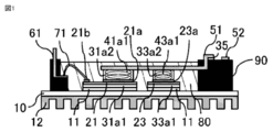
- FIG. 1 is a schematic cross-sectional view showing a semiconductor device according to the first embodiment of the present disclosure.
- FIG. 2 is a plan view showing the semiconductor device according to the first embodiment of the present disclosure.
- the portion covered with the sealing resin or the lead frame (electrode plate) is not actually visible, but for the sake of explanation, the sealing resin or the lead frame is transmitted and displayed by a hidden line.
- the semiconductor device includes an insulating substrate 10 as a substrate, semiconductor elements 21 and 23 arranged on the insulating substrate 10, main electrodes (electrodes) 21a and 22a of the semiconductor element 21, and a semiconductor.
- the first lead frame (electrode plate) 51 through which the main circuit current electrically connected to the main electrode 23a (electrode) of the element 23 flows and the control electrode 21b for controlling the semiconductor element 21 are electrically connected by wire wiring 71.
- the insulating substrate 10 is made of an insulating substrate such as a ceramic substrate having a high thermal conductivity such as aluminum nitride (AlN).
- AlN aluminum nitride
- the outer dimensions are 40 mm ⁇ 25 mm and the thickness is 0.6 mm.
- the insulating substrate 10 is not limited to aluminum nitride as long as insulating properties can be obtained.
- the insulating substrate 10 may be, for example, a ceramic substrate such as alumina (Al 2 O 3 ) or silicon nitride (Si 3 N 4). Further, the substrate may be a substrate other than ceramic, such as a glass epoxy substrate or a metal base substrate.
- a conductor layer 11 made of a metal having a high conductivity such as aluminum (Al) or an aluminum alloy is provided on the surface of the insulating substrate 10.
- a conductor layer (not shown) made of a metal having a high conductivity such as aluminum (Al) or an aluminum alloy may be provided on the back surface of the insulating substrate 10.
- the conductor layer 11 is made of, for example, aluminum having a thickness of 0.3 mm.
- the conductor layer on the front surface side and the conductor layer on the back surface side may be formed of different materials, but it is preferable that the conductor layer on the front surface side and the conductor layer on the back surface side are formed of the same material in order to reduce the manufacturing cost.
- the conductor layer 11 formed on the insulating substrate 10 is not limited to aluminum, and may be formed of, for example, copper (Cu) or a copper alloy.
- Ni nickel (Ni) (not shown), which is a metal material in which the solder gets wet on the surface of aluminum, is formed, for example, with a thickness of 5.0 ⁇ m, and the conductor layer 11 and the semiconductor elements 21 and 23 are used as the first joining member. Solders 31a1 and 33a1 are used for joining.
- the metal material to which the solder gets wet may be tin (Sn), gold (Au), silver (Ag) or the like, in addition to nickel (Ni).
- the conductor layer 11 is formed with a circuit pattern for passing a main circuit current through the semiconductor elements 21 and 23. Since the semiconductor elements 21 and 23 are bonded to the conductor layer 11 by the solders 31a1 and 33a1, the conductor layer 11 is preferably a metal having a high conductivity.
- the heat sink 12 that exhausts the heat generated by the semiconductor elements 21 and 23 to the outside of the semiconductor device and the conductor layer on the back side are soldered or the like. It may be joined by a joining member, and the conductor layer on the back side is preferably a metal having a high thermal conductivity.
- the semiconductor element 21 and the semiconductor element 23 are semiconductor switching elements for power such as diodes, IGBTs (Insulated Gate Bipolar Transistor), MOSFETs (Metal-Oxide-Semiconductor Field), and ICs (Integrate) for control. .. Further, a rectifying element such as an SBD (Schottky Barrier Diode), an SBJ (Schottky Barrier Junction), or a thyristor may be used.
- SBD Schottky Barrier Diode
- SBJ Schottky Barrier Junction
- the semiconductor element 21 is an IGBT formed of silicon (Si) and the semiconductor element 23 is a diode formed of silicon will be described.
- the external dimensions of the semiconductor element 21 are 15 mm ⁇ 15 mm, and the thickness is 100 ⁇ m.
- the external dimensions of the semiconductor element 23 are 10 mm ⁇ 15 mm, and the thickness is 100 ⁇ m.
- the semiconductor elements 21 and 23 may be formed of, for example, a semiconductor material such as silicon carbide (SiC) or gallium nitride (GaN).
- a semiconductor device having a 1in1 configuration in which the semiconductor device includes a pair of a semiconductor element 21 which is an IGBT and a semiconductor element 23 which is a diode will be described. It may be a 2in1 configuration semiconductor device having two pairs or a 6in1 configuration semiconductor device having six pairs. Further, it may be a semiconductor device provided with only the semiconductor element 21.
- the semiconductor device may be configured to include another semiconductor switching element such as a MOSFET instead of the IGBT.
- the semiconductor element 21 which is an IGBT and the semiconductor element 23 which is a diode have an electrode on the back surface (not shown) bonded to the insulating substrate 10 via a conductor layer 11 and a surface opposite to the electrode on the back surface. It is provided with a surface electrode provided in.
- Spacers made of aluminum wire (not shown) having a wire diameter of 100 ⁇ m are mounted at the four corners of the conductor layer 11 at the positions where the semiconductor elements 21 and 23 are joined. Join with 23.
- the spacer may be a Cu wire other than the Al wire.
- the wire diameter of the wire as a spacer is not limited to 100 ⁇ m as long as it is smaller than the thickness of the solder in the bonded state.
- a nickel ball may be used as the spacer as long as the minimum solder thickness can be secured. Further, it may be configured to be soldered without using a spacer.
- Solder 31a1 and 33a1 use a Sn / Ag / Cu system containing tin, silver and copper as main components.
- the external dimensions of the solder 31a1 are 15 mm ⁇ 15 mm
- the external dimensions of the solder 33a1 are 15 mm ⁇ 10 mm
- the thickness of the solders 31a1 and 33a1 after joining is 100 to 200 ⁇ m.
- solder materials include Sn / Ag-based materials containing tin and silver as main components, Sn / Cu-based materials containing tin and copper as main components, and tin and bismuth (Bi) as main components. It may be Sn / Bi system or the like. Further, the solders 31a1 and 33a1 may contain antimony (Sb), nickel (Ni), indium (In), bismuth, aluminum (Al), zinc (Zn) and the like. Although the effects of the present disclosure can be obtained even if the materials of the solders 31a1 and 33a1 contain lead (Pb), the solder containing lead is not preferable because it has a high environmental load.
- Pb lead
- the first joining members 31a1 and 33a1 for joining the conductor layer 11 and the semiconductor elements 21 and 23 are not limited to solder.
- a sintered material made of metal nanoparticles such as silver nanoparticles and copper nanoparticles may be used.
- Main electrodes 21a and 22a are formed as electrodes on the semiconductor element 21, that is, on the surface of the semiconductor element 21, and are bonded to the first lead frame 51 by solders 31a2 and 33a2 as second bonding members, respectively.
- the first lead frame 51 is arranged so as to face the surface of the semiconductor element 21.
- a main circuit current flows between the main electrodes 21a and 22a on the front surface of the semiconductor element 21 and the electrodes (not shown) on the back surface of the semiconductor element 21.
- a main electrode 23a as an electrode is formed on the semiconductor element 23, that is, on the surface of the semiconductor element 23.
- the main electrode 23a is joined to the first lead frame 51 by the solder 33a2 as the second joining member.
- a main circuit current flows between the main electrode 23a on the front surface of the semiconductor element 23 and the electrode (not shown) on the back surface of the semiconductor element 23.
- the main electrodes 21a, 22a, and 23a are configured to contain nickel (Ni) that can be joined by solder.
- Ni nickel
- Au gold
- silver Au
- Cu copper
- the main electrodes 21a, 22a, and 23a are nickel (Ni) and gold. It may be configured to contain at least one of (Au), silver (Ag), and copper (Cu).
- the main electrodes 21a and 22a are electrodes that are joined to the first lead frame 51 by solder and a large current main circuit current flows, and have a larger area than the control electrode 21b and the temperature sense electrode 22b described later.
- the first cylindrical coil springs (elastic members) 41a1 and 43b1 are compression springs.
- the first cylindrical coil springs (elastic members) 41a1 and 43b1 include a core material (not shown), a covering portion (not shown), and a metal-plated portion (not shown).
- the core material is made of a metal having a large elastic modulus.
- the core material is made of a metal having a higher elastic modulus than the covering portion. Therefore, the combination of the material of the core material and the material of the covering portion can widen the design range of the elastic modulus and the conductivity of the first cylindrical coil spring (elastic member).
- the core material has a cylindrical shape.
- the wire diameter of the core material is, for example, 0.1 mm.
- the material of the core material is a metal having a large elastic modulus, although it does not necessarily have a large conductivity.
- the material of the core material contains a metal such as stainless steel or tungsten (W). Further, the material of the core material is not limited to stainless steel or tungsten (W), and may be spring steel.
- the covering part covers the circumference of the core material.
- the coating is made of a metal having high conductivity.
- the covering portion is made of a metal having a higher conductivity than the core material.
- the material of the covering portion contains, for example, a metal such as aluminum (Al).
- the material of the covering portion is not limited to aluminum (Al), and may be any metal having a large conductivity such as an aluminum (Al) alloy and copper (Cu).
- the metal-plated part (not shown) is applied to the surface of the covering part.
- the metal-plated portion covers the coating portion.
- the thickness of the metal-plated portion is, for example, 0.5 ⁇ m.
- the material of the metal plating part is a metal that gets wet with solder.
- the material of the metal plating portion contains, for example, nickel (Ni).
- the material of the metal plating portion is not limited to nickel (Ni), and may be, for example, a metal containing at least one of tin (Sn), gold (Au), silver (Ag) and copper (Cu).
- first cylindrical coil springs 41a1 and 43a1 have a configuration containing at least one of aluminum (Al) and copper (Cu), they become elastic members having high conductivity and can be energized with a large current. Further, at least a part of the surface of the first cylindrical coil springs 41a1 and 43a1 is metal-plated with at least one of tin (Sn), gold (Au), silver (Ag) and copper (Cu). If this is the case, in the step of joining the first cylindrical coil springs 41a1 and 43a1, the solder can be more effectively adhered to the outermost surfaces of the first cylindrical coil springs 41a1 and 43a1 to improve the wettability.
- the first cylindrical coil springs 41a1 and 43a1 are provided between the front surface of the semiconductor elements 21 and 23 and the back surface of the first lead frame 51, respectively.
- One end of the first cylindrical coil springs 41a1 and 43a1 is in line contact with the main electrodes 21a and 22a formed on the surface of the semiconductor element 21, and the other end is in line contact with the first lead frame 51, and both ends have a curved shape.
- It is a conductive elastic member having an included elastic force.
- the first cylindrical coil springs 41a1 and 43a1 are provided between the front surface of the semiconductor element 21 and the back surface of the first lead frame 51, the outer diameter, free length, close contact length, etc. of the cylindrical coil spring are required. The value can be easily adjusted. Therefore, as shown in FIG. 1, the first cylindrical coil springs 41a1 and 43a1 are set so that the respective distances between the front surfaces of the semiconductor elements 21 and 23 and the back surface of the first lead frame 51 are desired values. Is provided.
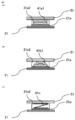
- FIG. 3 is a schematic cross-sectional view of a part of the semiconductor device according to the first embodiment of the present disclosure.
- FIG. 3A is an enlarged cross-sectional schematic view of the first cylindrical coil spring 41a1 (elastic member) and its periphery.
- FIG. 3B is an enlarged cross-sectional schematic view of the first conical coil spring 41b1 (elastic member) and its periphery.
- FIG. 3C is an enlarged cross-sectional schematic view of the first leaf spring 41c (elastic member) and its periphery.
- the first cylindrical coil spring 41a1 is provided between the main electrode 21a formed on the surface of the semiconductor element 21 and the first lead frame 51, and one end thereof is the main electrode 21a. The other end is line-contacted with the first lead frame 51, and both ends have an elastic force and conductivity including a curved shape having an arc shape. Since many wire rods having different outer shapes are distributed depending on the application, the coil spring can be easily selected as a spring provided between the main electrode 21a and the first lead frame 51. Further, the cylindrical coil spring is a coil spring including a curved shape having an arc shape having the same outer diameter at both ends, and can be easily manufactured. Further, the cylindrical coil spring can stably support the main electrode 21a and the first lead frame 51.
- the shape of the elastic member when the distance between the semiconductor element 21 and the first lead frame 51 is larger than the specified value, it is sufficient that the generation of the unbonded portion due to the solder 31a2 can be suppressed. It may have a shape as shown in c).
- the first conical coil spring 41b1 is provided between the main electrode 21a formed on the surface of the semiconductor element 21 and the first lead frame 51, and one end thereof is the main electrode 21a.
- the other end is in line contact with the first lead frame 51, and both ends have a curved shape having a spiral shape and have elastic force and conductivity.
- a conical coil spring is a coil spring that includes a curved shape having a spiral shape with different outer diameters at both ends. Therefore, by designing the wires so that they do not come into close contact with each other during compression, the close contact length can be made shorter than that of a cylindrical coil spring. Therefore, even if the cylindrical coil spring cannot be provided due to the limitation of the distance between the semiconductor element 21 and the first lead frame 51, the conical coil spring can be provided.
- the shape of the elastic member does not have to be the shape of the coil spring shown in FIGS. 3 (a) and 3 (b).
- the shape may be a leaf spring having a planar shape at both ends and having a plurality of contacts.
- the first leaf spring 41c obtained by bending a metal plate is provided between the main electrode 21a formed on the surface of the semiconductor element 21 and the first lead frame 51, and has one end. Is in surface contact with the main electrode 21a and the other end is in surface contact with the first lead frame 51, and both ends have a planar shape and have elastic force and conductivity.
- the surfaces at both ends of the first leaf spring 41c have a uniform width and a uniform plate thickness.
- the leaf spring Since the leaf spring has a planar shape at both ends, it comes into surface contact with the main electrode 21a or the first lead frame 51. That is, in the leaf spring, the area where one end contacts the main electrode 21a and the other end contacts the first lead frame 51 is such that one end of the cylindrical coil spring or the conical coil spring, which is a coil spring, is in contact with the main electrode 21a. The end is wider than the area in contact with each of the first lead frames 51. Since the solder 31a2 wets and spreads through the first leaf spring 41c, the area in contact with the main electrode 21a or the first lead frame 51 also increases. Therefore, the leaf spring can suppress the generation of the unbonded portion due to the solder 31a2 as compared with the coil spring.
- the leaf spring can be processed into a more complicated shape than the coil spring. Therefore, the leaf spring can be processed in consideration of the shape of the semiconductor element 21 or the first lead frame 51. Further, since the leaf spring has a larger contact area with the semiconductor element 21 and the first lead frame 51 than the coil spring, it can cope with energization of a large current.
- the solder 31a2 is provided between the main electrode 21a formed on the surface of the semiconductor element 21 and the first lead frame 51, and the main electrode 21a and one end of the elastic member are separated from the first lead frame 51 and the elastic member. The other ends of the solder are joined to each other to have conductivity.
- the solder 31a2 may be formed by joining the main electrode 21a and one end of the elastic member, and the first lead frame 51 and the other end of the elastic member, respectively.
- the solder 31a2 covers the elastic member, the first cylindrical coil spring 41a1, the first conical coil spring 41b1, or the first leaf spring 41c. It suffices if it is provided in.
- both ends of the elastic member are preferably a coil spring including a curved shape or a leaf spring including a planar shape.
- one end or the other end of the elastic member has a convex shape, for example, one end of the elastic member and the main electrode 21a, or the other end of the elastic member and the first lead frame 51 come into point contact. Become.
- the distance between the main electrode 21a and the first lead frame 51 is larger than specified, one end of the elastic member and the main electrode 21a, or the other end of the elastic member and the first lead frame 51 are points. Even if they come into contact with each other, the solder does not sufficiently wet and spread to the main electrode 21a or the first lead frame 51 which is point-contacted via the elastic member.
- the first cylindrical coil spring 41a1 shown in FIG. 3A has an outer diameter of 3.0 mm, a core material thickness of 0.1 mm, a free length of 1.0 mm, and a close contact length of 0.2 mm. To do. As described above, if the free length of the first cylindrical coil spring 41a1 is 1.0 mm and the close contact length is 0.2 mm, the main electrode 21a formed on the surface of the semiconductor element 21 and the first lead frame 51 When the distance becomes larger than the specified distance by about 0.2 mm, the first cylindrical coil spring 41a1 extends by the distance larger than the specified distance, so that one end of the first cylindrical coil spring 41a1 and the main electrode With 21a, the other end of the elastic member and the first lead frame 51 are in line contact with each other.
- the solder 31a2 can sufficiently wet and spread on the main electrode 21a and the first lead frame 51 which are line-contacted via the first cylindrical coil spring 41a1 and can suppress the generation of unbonded portions due to the solder.
- FIGS. 3A to 3C have been described as a configuration in which one elastic member is provided between the main electrode 21a formed on the surface of the semiconductor element 21 and the first lead frame 51, the elastic member May be configured to be provided in parallel. Further, the configurations of FIGS. 3 (a) to 3 (c) may be combined with each other.
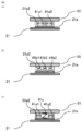
- FIG. 4 is a schematic cross-sectional view of a part of the semiconductor device according to the first embodiment of the present disclosure.
- FIG. 4A is a schematic cross-sectional view in which a total of two first cylindrical coil springs 41a1 and 41a2 are provided in parallel, and the periphery thereof is also enlarged.
- FIG. 4B is a schematic cross-sectional view in which a total of three first conical coil springs 41b1, 41b2, and 41b3 are provided in parallel, and the periphery thereof is also enlarged.
- FIG. 4C is a schematic cross-sectional view in which a total of three first cylindrical coil springs 41a1, a first leaf spring 41c, and a first cylindrical coil spring 41a2 are provided in parallel, including their periphery. ..
- the elastic member has been described as having a cylindrical coil spring, a conical coil spring, or a disc spring, but one end of the elastic member is the main electrode 21a and the other end is the first.
- the lead frame 51 may be in line contact or surface contact with each other to have elastic force, and may be, for example, a disc spring (not shown).
- Belleville springs like leaf springs described above, include planar shapes at both ends. Therefore, the disc spring comes into surface contact with the main electrode 21a or the first lead frame 51. That is, in the leaf spring, the area where one end contacts the main electrode 21a and the other end contacts the first lead frame 51 is wider than that of a cylindrical coil spring or a conical coil spring which is a coil spring. Therefore, it is possible to energize a larger current than the coil spring.
- a control electrode 21b for controlling a control signal and a temperature sense electrode 22b for measuring the temperature of the semiconductor element are formed on the semiconductor element 21 so as to be separated from each of the main electrodes 21a and 22a. ing. That is, the main electrode 21a and the control electrode 21b, and the main electrode 21a and the temperature sense electrode 22b are formed on the semiconductor element 21 so as to be separated from each other. Further, the main electrode 22a and the control electrode 21b, and the main electrode 22a and the temperature sense electrode 22b are formed so as to be separated from each other on the surface of the semiconductor element 21.
- main electrodes 21a and 22a as the main electrodes on the semiconductor element 21
- one main electrode and the control electrode 21b are formed apart from each other, and one main electrode and the temperature sense electrode 22b are formed apart from each other.
- control electrode 21b and the second lead frame 61 are electrically connected by a wire wiring 71, and the continuity and interruption of the main circuit current are controlled based on the input control signal. Further, the temperature sense electrode 22b and the second lead frame 62 are electrically connected by the wire wiring 72.
- the wire wirings 71 and 72 may be, for example, an aluminum wire having a diameter of 0.15 mm, an aluminum-coated copper wire, or a gold wire.
- the wire wiring 71 is ultrasonically bonded to the second lead frame 61 and the control electrode 21b by wire bonding. Further, the wire wiring 72 is ultrasonically bonded to the second lead frame 62 and the temperature sense electrode 22b by wire bonding.
- an electrode such as an emitter current sense electrode may be provided on the surface of the semiconductor element 21 to measure the current of the emitter. Even if there is an emitter current sense electrode, it is electrically connected by wire wiring like the control electrode 21b and the like. As shown in FIG. 2, it is preferable that the electrodes for wire wiring are arranged in a row along one side of the semiconductor element 21 because ultrasonic bonding is easily performed.
- the first lead frame 51 as the plate-shaped electrode plate shown in FIGS. 1 and 2 is made of, for example, copper (Cu) or a copper alloy having a thickness of 1.0 mm, and the first cylindrical coil spring 41a1. Is in contact with one end of the main electrodes 21a and 22a formed on the surface of the semiconductor element 21, and is joined by solder 31a2. Further, the first lead frame 51 is in contact with one end of the first cylindrical coil spring 41a1 and is joined to the main electrode 23a provided on the surface of the semiconductor element 23 by the solder 33a2.
- the first lead frame 51 is made of aluminum (Al) or an aluminum alloy that does not allow the solder to get wet.
- the first lead frame 51 has a structure in which a metal material such as copper (Cu) or a copper alloy that gets wet with solder is formed on the solder joint portion, or a metal such as nickel (Ni) or gold (Au) is formed on the surface of the solder joint portion. It may be formed. Further, the first lead frame 51 may use a clad material in which a plurality of metals such as Invar are bonded together.
- the first lead frame 51 which is a plate-shaped electrode plate, is described, but the electrode plate may be, for example, a printed circuit board having a wiring pattern.
- the solders 31a2 and 33a2 use a Sn / Ag / Cu system containing tin, silver, and copper as main components.
- the length of the long side is 6 to 9 mm
- the length of the short side is 4 to 5 mm
- the length of one side of the external dimensions of the solder 33a2 is 9 to 12 mm for the long side and 9 to 12 mm for the short side.
- the length is 6-8 mm.
- the thickness of the solder 31a2 after joining is set based on the distances defined between the main electrodes 21a and 22a and the first lead frame 51, respectively.
- the thickness of the solder 33a2 after joining is set based on the distance defined between the main electrode 23a and the first lead frame 51.
- the thickness of the solders 31a2 and 33a2 after joining is 300 to 500 ⁇ m.
- the Sn / Cu type containing tin and copper as main components, the Sn / Ag type containing tin and silver as main components, and the like are used as the materials of the solders 31a1 and 33a1 described above. You can also do it.
- the contact angle when the solders 31a2 and 33a2 and the first cylindrical coil springs 41a1 come into contact with each other is less than 90 °. Is preferable.
- a terminal plate 53 made of a metal having a high conductivity such as copper (Cu) or a copper alloy is bonded to the conductor layer 11 by a method such as ultrasonic bonding.
- the terminal plate 53 is provided with a main terminal 54, and the main terminal 54 is fixed to the case 90.
- the electrodes on the back surfaces of the semiconductor elements 21 and 23 and the main terminal 54 are electrically connected.
- the first lead frame 51 is provided with a main terminal 52 used for electrical connection with an external device at an end opposite to the side joined to the semiconductor elements 21 and 23, and the main terminal 52 Is fixed to the case 90.
- the main terminal 52 and the main terminal 54 are electrically connected via the conductor layer 11, the semiconductor elements 21, 23, and the first lead frame 51, and the main circuit current is connected between the main terminal 52 and the main terminal 54. Will be able to flow.
- the second lead frames 61 and 62 are made of copper (Cu) or a copper alloy or aluminum (Al) or an aluminum alloy and are fixed to the case 90. One end of the second lead frames 61 and 62 is exposed to the outside of the semiconductor device, and the second lead frame 61 is a control terminal for inputting a control signal.
- the second lead frame 62 is a terminal for measuring the temperature of the semiconductor element 21.
- the control terminals exposed to the outside of the semiconductor device are plated with copper (Cu) or nickel (Ni) and soldered. You may improve the wettability of the solder.
- the other end of the second lead frame 61 is electrically connected to the control electrode 21b provided on the surface of the semiconductor element 21 by a wire wiring 71.
- the other end of the second lead frame 62 is electrically connected by a temperature sense electrode 22b and a wire wiring 72 provided on the surface of the semiconductor element 21.
- the first lead frame 51 and the second lead frames 61 and 62 as the plate-shaped wiring member have been described as an example of being embedded and fixed in the case 90, but the first lead frame 51 has been described.
- the end on the side opposite to the side joined to the semiconductor elements 21 and 23 and the end on the side opposite to the side on which the wire wiring 71 of the second lead frame 61 is joined are formed in advance in the case 90. It may be configured to be connected to the electrode terminal with solder or a conductive adhesive.
- the case 90 is formed in a frame shape by PPS (Polyphenylene Sulfide) resin, surrounds the outer periphery of the surface of the insulating substrate 10 on which the semiconductor elements 21 and 23 are mounted, and is adhered to the insulating substrate 10.
- the case 90 may be formed of PBT (PolyButylene terephate) or the like as long as it is not deformed by heat when the solders 31a1, 31a2, 33a1 and 33a2 are heated and melted.
- the sealing resin portion 80 is formed of an epoxy resin, and includes a conductor layer 11, semiconductor elements 21, 23, a part of the first lead frame 51, a part of the second lead frame 61, and a wire wiring 71. , 72, and the solders 31a1, 31a2, 33a1, 33a2 are covered and hermetically sealed.
- the sealing resin forming the sealing resin portion 80 is not limited to the epoxy resin as long as the insulating property can be ensured.
- the sealing resin may be, for example, a liquid gel or the like.
- the sealing method using a resin material may be a sealing method using a transfer mold, in addition to the sealing method using the case 90 and the sealing resin portion 80 described above.
- the case 90 and the insulating substrate 10 have holes for joining the heat sink 12 which is a cooling plate, and screws (not shown) are joined to the heat sink 12 through the holes.
- the insulating substrate 10 may be bonded to the heat sink 12 on the back surface via grease or a heat radiating sheet. It should be noted that the heat radiating sheet does not require wiping work as compared with grease, and it is preferable that the heat radiating sheet has a thickness of 0.4 mm or less and a thermal conductivity of 1 W / mK or more.
- the heat sink 12 is made of aluminum (Al) or an aluminum alloy.
- the surface of the heat sink 12 is joined to the case 90 and the insulating substrate 10 through screws (not shown).
- a plurality of cooling fins are arranged on the back surface of the heat sink 12, and heat generation in the semiconductor elements 21 and 23 can be suppressed.
- the heat sink 12 preferably has a thermal conductivity of 100 W / mK or more.
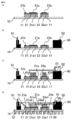
- FIG. 5 is a schematic cross-sectional view showing a method of manufacturing a semiconductor device according to the first embodiment of the present disclosure.
- the solder 31a1 and the semiconductor element 21 as the first bonding member are arranged on the conductor layer 11 provided on the surface of the insulating substrate 10.
- the solder 33a1 and the semiconductor element 21 as the first joining member are arranged on the conductor layer 11 provided on the surface of the insulating substrate 10.
- an electrode (not shown) on the back surface of the semiconductor element 21 having an electrode or the like formed on the front surface is attached to the conductor layer 11 provided on the surface of the insulating substrate 10 as a first bonding member.
- Solder 31a1 is joined by heating.
- the electrodes (not shown) on the back surface of the semiconductor element 23 having the electrodes formed on the front surface are bonded to the conductor layer 11 on the insulating substrate 10 with the solder 33a1 as the first bonding member.
- the insulating substrate 10 to which the semiconductor elements 21 and 23 are bonded is arranged on the bottom of the frame-shaped case 90. Then, the case 90 is adhesively fixed on the insulating substrate 10 with an adhesive material made of silicon (not shown).
- the case 90 is provided with a second lead frame 61 by insert molding in advance, and the main terminal 52 is fixed to the upper part of the case 90.
- the case 90 is also provided with a second lead frame 62.
- a terminal plate 53 is also provided in advance in the case 90, and the main terminal 54 provided in the terminal plate 53 is fixed to the upper part of the case 90.
- the second lead frame 62 is at a position corresponding to the temperature sense electrode 22b of the semiconductor element 21 whose wire bonding portion is bonded to the insulating substrate 10. It is fixed to the case 90.
- a plate solder which is a second bonding member, is placed on the main electrode 21a formed on the surface of the semiconductor element 21 bonded to the insulating substrate 10.
- a solder 31a2 made of the material is arranged, and a first cylindrical coil spring 41a1 which is an elastic member is arranged on the solder 31a2.
- solder 31a2 made of plate solder, which is a second joining member is also arranged on the main electrode 22a. Then, the first cylindrical coil spring 41a1 which is an elastic member is arranged on the first cylindrical coil spring 41a1.
- solder 33a2 made of plate solder, which is a second bonding member, is arranged on a main electrode 23a formed on the surface of the semiconductor element 23 bonded to the insulating substrate 10, and a second elastic member is placed on the solder 33a2.
- One cylindrical coil spring 43a1 is arranged.
- a solder 35 made of plate solder, which is a joining member, is arranged on the upper part of the case 90 so that the first lead frame 51 and the case 90 are connected to each other. Then, the first lead frame 51 is arranged on the solders 31a2, 33a2, and 35.
- the solders 31a2, 33a2, and 35 are heated and melted by a reflow furnace or a hot plate, and the main electrodes 21a, 23a, and the case 90 and the first lead frame 51 are solder-joined. ..
- the first cylindrical coil spring 41a1 and 43a1 does not melt.
- one end of the first cylindrical coil spring 41a1 is connected to the main electrode 21a and the other end is connected to the first lead frame 51 between the surface of the semiconductor element 21 and the first lead frame 51. They are joined by contact or surface contact. Further, between the surface of the semiconductor element 23 and the first lead frame 51, one end of the first cylindrical coil spring 43a1 is in line contact with the main electrode 23a, and the other end is in line contact with the first lead frame 51, respectively. They are contacted and joined.
- solder When solder is used for the first joining members 31a1 and 33a1, if a material in which the melting points of the solders 31a2 and 33a2 are lower than the melting points of the solders 31a1 and 33a1 is selected, the semiconductor elements 21 and 23 and the first lead frame are selected. When the 51 is solder-bonded, even if the semiconductor elements 21 and 23 and the conductor layer 11 are already bonded by the solders 31a1 and 33a1, the solders 31a1 and 33a1 are not remelted, which is preferable.
- wires are bonded on the control electrode 21b of the semiconductor element 21 and on the second lead frame 61 by wire bonding by ultrasonic bonding. That is, the control electrode 21b of the semiconductor element 21 and the second lead frame 61 are electrically connected by the wire wiring 71.
- the temperature sense electrode 22b of the semiconductor element 21 and the second lead frame 62 are electrically connected by wire wiring 72.
- the terminal plate 53 and the conductor layer 11 provided on the insulating substrate 10 are bonded by ultrasonic bonding.
- the bonding by ultrasonic bonding may be performed before or after the solder bonding between the main electrodes 21a and 23a on the surfaces of the semiconductor elements 21 and 23 and the first lead frame 51.
- the semiconductor elements 21 and 23 are electrically connected between the main terminal 52 and the main terminal 54 of the semiconductor device.
- a sealing resin portion 80 is formed in the case 90 with a potting resin, and the semiconductor elements 21 and 23 and the first lead frame 51 are insulated and sealed in the case 90.
- the case 90 and the insulating substrate 10 have holes for joining the heat sink 12 which is a cooling plate. Finally, as a cooling plate joining step, the case 90 and the insulating substrate 10 are joined to the heat sink 12 which is a cooling plate through screws (not shown). That is, the semiconductor device is completed by joining the back surface of the insulating substrate 10 and the heat sink 12.
- the semiconductor element 21 As described above, according to the first embodiment of the present disclosure, it is provided between the semiconductor element 21 and the first lead frame 51, one end of which is the main electrode 21a and the other end of which is the first lead frame 51.
- a conductive solder 31a2 for joining the other ends of the first cylindrical coil spring 41a1 is provided.
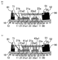
- 6 and 7 are schematic cross-sectional views for explaining the effect of the semiconductor device according to the first embodiment of the present disclosure.
- FIG. 6 shows the semiconductor device according to the first embodiment of the present disclosure when the distance between the semiconductor elements 21 and 23 and the first lead frame 51 becomes larger than specified due to the deformation of the insulating substrate 10 during solder mounting. It is sectional drawing to explain the effect.
- the semiconductor element is heated.
- the heat sink 12 to which the insulating substrate 10 is bonded is also heated.
- the coefficient of thermal expansion of nickel (Ni), tin (Sn), gold (Au), or silver (Ag) contained in the conductor layer 11 provided on the surface of the insulating substrate 10 is aluminum (Al) contained in the heat sink 12. Since it is smaller than the coefficient of thermal expansion of, the insulating substrate 10 may be deformed so as to be convex in the direction of the heat sink 12.
- the distances between the main electrodes 21a and 23a and the first lead frame 51 are larger than specified respectively. Therefore, between the main electrodes 21a and 23a and the first lead frame 51, unbonded portions due to the solders 31a2 and 33a2 are generated.
- the first cylindrical coil springs 41a1 and 43a1 which are elastic members are provided between the main electrodes 21a and 23a and the first lead frame 51, respectively. Even if the insulating substrate 10 is deformed so as to be convex in the direction of the heat sink 12, the first cylindrical coil springs 41a1 and 43a1 extend according to the degree of deformation of the insulating substrate 10, and one end thereof becomes the main electrodes 21a and 23a. The other end is in line contact or surface contact with the first lead frame 51, respectively. Then, the solder 31a2 joins the main electrode 21a and one end of the first cylindrical coil spring 41a1 and the other end of the first lead frame 51 and the first cylindrical coil spring 41a1.
- solder 33a2 joins the main electrode 21a and one end of the first cylindrical coil spring 43a1 and the other end of the first lead frame 51 and the first cylindrical coil spring 43a1. Since one end of the first cylindrical coil springs 41a1 and 43a1 is in line contact or surface contact with the main electrodes 21a and 23a and the other end with the first lead frame 51, the solders 31a2 and 33a2 are first. Along the cylindrical coil springs 41a1 and 43a1 of the above, the main electrodes 21a and 23a and the first lead frame 51 are wetted and spread, respectively. Therefore, the generation of unbonded portions due to the solders 31a2 and 33a2 is suppressed.
- the coefficient of thermal expansion of the insulating substrate 10 may be larger than the coefficient of thermal expansion of the heat sink 12 depending on the type of metal on which the insulating substrate 10 and the heat sink 12 are formed.
- the insulating substrate 10 is deformed so as to be convex in the direction opposite to that of the heat sink 12. Therefore, the distances between the main electrodes 21a and 23a and the first lead frame 51 are smaller than specified, but the first cylindrical coil springs 41a1 and 43a1 contract according to the degree of deformation of the insulating substrate 10, and one end thereof is The other end of the main electrode 21a is in line contact or surface contact with the first lead frame 51, respectively.
- the solders 31a2 and 33a2 are the main electrodes 21a and 23a and the first lead frame along the first cylindrical coil springs 41a1 and 43a1, respectively. It spreads wet to 51, and the generation of unbonded portions due to the solders 31a2 and 33a2 is suppressed.
- FIG. 7 shows the implementation of the present disclosure when the distance between the semiconductor elements 21 and 23 and the first lead frame 51 becomes larger than specified due to manufacturing variations when the first lead frame 51 is joined to the case 90. It is sectional drawing for demonstrating the effect of the semiconductor device in Embodiment 1.
- FIG. 7 shows the implementation of the present disclosure when the distance between the semiconductor elements 21 and 23 and the first lead frame 51 becomes larger than specified due to manufacturing variations when the first lead frame 51 is joined to the case 90. It is sectional drawing for demonstrating the effect of the semiconductor device in Embodiment 1.
- FIG. 7 shows the implementation of the present disclosure when the distance between the semiconductor elements 21 and 23 and the first lead frame 51 becomes larger than specified due to manufacturing variations when the first lead frame 51 is joined to the case 90. It is sectional drawing for demonstrating the effect of the semiconductor device in Embodiment 1.
- FIG. 7 shows the implementation of the present disclosure when the distance between the semiconductor elements 21 and 23 and the first lead frame 51 becomes larger than specified due to manufacturing variations when the first lead frame 51 is joined to the case 90.
- the first lead frame 51 when the first lead frame 51 is joined to the case 90 with the solder 35, it is originally joined to the position where the first lead frame 51 is joined due to manufacturing variations. There may be a gap between the position and the position. Therefore, the distance between the main electrodes 21a and 23a and the first lead frame 51 becomes larger than specified, respectively, and the main electrodes 21a and 23a and the first lead frame 51 are not joined by solders 31a2 and 33a2, respectively. Part will occur.
- the first cylindrical coil springs 41a1 and 43a1 which are elastic members are provided between the main electrodes 21a and 23a and the first lead frame 51, respectively. Even if there is a deviation between the position where the first lead frame 51 is joined and the position where the first lead frame 51 is originally joined, the first cylindrical coil springs 41a1 and 43a1 are adjusted to the degree of deviation of the first lead frame 51, respectively. It extends and has one end in line contact or surface contact with the main electrodes 21a and 23a and the other end with the first lead frame 51, respectively. Then, the solder 31a2 joins the main electrode 21a and one end of the first cylindrical coil spring 41a1 and the other end of the first lead frame 51 and the first cylindrical coil spring 41a1.
- solder 33a2 joins the main electrode 21a and one end of the first cylindrical coil spring 43a1 and the other end of the first lead frame 51 and the first cylindrical coil spring 43a1. Since one end of the first cylindrical coil springs 41a1 and 43a1 is in line contact or surface contact with the main electrodes 21a and 23a and the other end with the first lead frame 51, the solders 31a2 and 33a2 are first. Along the cylindrical coil springs 41a1 and 43a1 of the above, the main electrodes 21a and 23a and the first lead frame 51 are wetted and spread, respectively. Therefore, the generation of unbonded portions due to the solders 31a2 and 33a2 is suppressed.
- the distances between the main electrodes 21a and 23a and the first lead frame 51 are different depending on the manufacturing variation. It may be smaller than specified.
- the first cylindrical coil springs 41a1 and 43a1 contract according to the degree of deviation of the first lead frame 51, and one end is in line contact with the main electrode 21a and the other end is in line contact with the first lead frame 51, respectively. Face contact.
- the solders 31a2 and 33a2 are the main electrodes along the first cylindrical coil springs 41a1 and 43a1, respectively. It spreads wet to the 21a and 23a and the first lead frame 51, and the generation of unbonded portions due to the solders 31a2 and 33a2 is suppressed.
- the deformation of the insulating substrate 10 at the time of solder mounting as shown in FIG. 6A and the first lead frame 51 as shown in FIG. 7A are joined to the case 90.
- manufacturing variations may occur, and the distances between the main electrodes 21a and 23a and the first lead frame 51 may be out of the specified range.
- the first cylindrical coil springs 41a1 and 43a1 expand and contract according to the degree of deformation of the insulating substrate 10 and the degree of deviation of the first lead frame 51, and one end of the main electrode 21a, The other end of the 23a is in line contact or surface contact with the first lead frame 51, respectively.
- solders 31a2 and 33a2 wet and spread on the main electrodes 21a and 23a and the first lead frame 51 along the first cylindrical coil springs 41a1 and 43a1, respectively, and unbonded portions are generated by the solders 31a2 and 33a2. It is suppressed.
- FIG. 8 is a schematic cross-sectional view of a part of the semiconductor device according to the second embodiment of the present disclosure.
- 8 (a) and 8 (b) are schematic cross-sectional views of the first cylindrical coil spring 41a1 (elastic member) and its periphery.
- the configuration of the first lead frame 51 which is an electrode plate, is different from that of the first embodiment.
- Other configurations of the semiconductor device of the second embodiment are the same as the configurations of the semiconductor device of the first embodiment.
- the holding portion for holding the elastic member provided between the surface of the semiconductor element 21 and the first lead frame 51 will be described here, the following description describes the surface of the semiconductor element 23 and the first lead. Needless to say, the same applies to the holding portion for holding the elastic member provided between the frame 51 and the frame 51.
- a protruding portion 51a projecting in the direction of the semiconductor element 21 is provided as a holding portion at a position in contact with the end portion of the first cylindrical coil spring 41a1.
- a convex structure is provided as the holding portion.
- the protruding portion 51a is provided at a position for holding the first cylindrical coil spring 41a1 when viewed from a direction perpendicular to the surface of the first lead frame 51, in a shape including a curved line formed of an arc.
- the protruding portion 51a is provided at a position including at least a part of the main electrode 21a in the plan view of the semiconductor element 21 viewed from above, that is, in the plan view of the semiconductor element 21 viewed from the first lead frame 51.
- the protruding portion 51a is a main electrode 22a in a plan view of the semiconductor element 21 viewed from above, that is, a plan view of the semiconductor element 21 viewed from the first lead frame 51. It is provided at a position including a part. The other end of the first cylindrical coil spring 41a1 is held by the protrusion 51a.
- the first lead frame 51 was buried as a holding portion in the direction opposite to that of the semiconductor element 21 at a position in contact with the end portion of the first cylindrical coil spring 41a1.
- the configuration may be such that the buried portion 51b is provided. That is, a concave structure is provided as the holding portion.
- the elastic member (first cylindrical coil spring 41a) By inserting the elastic member (first cylindrical coil spring 41a) into the concave structure, the elastic member (first cylindrical coil spring 41a) can be joined to the electrode plate (first lead frame 51).
- the buried portion 51b is provided at a position for holding the first cylindrical coil spring 41a1 when viewed from a direction perpendicular to the surface of the first lead frame 51, in a shape including a curved line formed of an arc.
- the buried portion 51b is provided at a position including at least a part of the main electrode 21a in a plan view of the semiconductor element 21 viewed from above, that is, a plan view of the semiconductor element 21 viewed from the first lead frame 51.
- the buried portion 51b is a main electrode 22a in a plan view of the semiconductor element 21 viewed from above, that is, a plan view of the semiconductor element 21 viewed from the first lead frame 51. It is provided at a position including a part. The other end of the first cylindrical coil spring 41a1 is held by the protrusion 51a.
- the protruding portion 51a and the buried portion 51b can be formed by half punching. Further, the protruding portion 51a can also be formed by joining or adhering a metal member different from the first lead frame 51 to a position where the first cylindrical coil spring 41a1 is held in the first lead frame 51. Is.
- the protruding portion 51a or the buried portion 51b which is the holding portion, has the first cylindrical coil spring 41a1.
- the protruding portion 51a or the buried portion 51b may include any shape such as a circular shape, a curved line consisting of an elliptical arc, an elliptical shape, a quadrangle, a substantially quadrangular shape, or a polygonal shape.
- the leaf spring having a quadrangular both ends and having a planar shape is provided so that the buried portion 51b has no gap. Can be held.
- the first lead frame 51 holds the first cylindrical coil spring 41a1 at a position in contact with the other end of the first cylindrical coil spring 41a1. Has a holding part.
- the first cylindrical coil spring 41a1 is arranged between the first lead frame 51 and the main electrodes 21a and 22a, and the cylindrical coil spring 41 is defined when the solder 41 melts in the elastic member joining step. It is expected that there will be a deviation. In this case, the protruding portion 51a or the buried portion 51b holds the first cylindrical coil spring 41a1. Therefore, the positioning accuracy of the first cylindrical coil spring 41a1 is improved by the protruding portion 51a or the buried portion 51b. As a result, when the solder 41 is melted, it is possible to prevent the first cylindrical coil spring 41 from deviating from the specified position, and it is possible to obtain a uniform contact pressure and a wet spread of the solder.
- the contact pressure between the first cylindrical coil spring 41a1 and the first lead frame 51 is obtained by increasing the gap between the first lead frame 51 and the main electrodes 21a and 22a. Even if this is not the case, the first cylindrical coil spring 41a wound around the protruding portion 51a or the first cylindrical coil spring 41a inserted into the buried portion 51b is attached to the first lead frame 51. It is in contact with the provided protruding portion 51a or the buried portion 51b.
- the cylindrical coil spring 41a can be joined to the first lead frame 51. Therefore, in a configuration in which the first lead frame 51 has a protruding portion 51a or a buried portion 51b, one end of the first cylindrical coil spring 41a1 is in line contact with the main electrode 21a, and the other end is in line contact with the first lead frame 51. And joined by solder 31a2, a highly reliable semiconductor device can be obtained.
- FIG. 9 is a schematic view showing an elastic member in which a coating film is formed by the joining member according to the third embodiment of the present disclosure.
- the solder coating 32 is formed on the first cylindrical coil spring 41a1, the first conical coil spring 41b1, or the first leaf spring 41c, which are elastic members.
- Other configurations of the semiconductor device of the third embodiment are the same as the configurations of the semiconductor device of the first embodiment.
- FIG. 9A is a schematic view showing a second cylindrical coil spring 41d as a joint coating elastic member.
- the second cylindrical coil spring 41d has a solder coating 32 formed so as to cover the first cylindrical coil spring 41a1.
- FIG. 9B is a schematic view showing a second conical coil spring 41e as a joint coating elastic member. A solder coating 32 is formed so as to cover the first conical coil spring 41b1.
- FIG. 9C is a schematic view showing a second leaf spring 41f as a joint coating elastic member. A solder coating 32 is formed so as to cover the first leaf spring 41c.
- the second cylindrical coil spring 41d, the second conical coil spring 41e, and the second leaf spring 41f are the first cylindrical coil spring 41a1, the first conical coil spring 41b1, and the first plate as core materials. It is a clad material in which a solder coating 32 made of plate solder is bonded so as to cover the spring 41c.
- FIG. 10 is a schematic cross-sectional view showing a method of manufacturing a semiconductor device according to the third embodiment of the present disclosure.
- a bonding film is formed on the main electrode 21a formed on the surface of the semiconductor element 21 bonded to the insulating substrate 10.
- a second cylindrical coil spring 41d which is an elastic member, is arranged.
- a second cylindrical coil spring 41d which is a joint coating elastic member, is also arranged on the main electrode 22a.
- a second cylindrical coil spring 43d which is a bonding coating elastic member, is arranged on the main electrode 23a formed on the surface of the semiconductor element 23 bonded to the insulating substrate 10.
- solder 35 made of plate solder, which is a joining member, is arranged on the upper part of the case 90 so as to be connected to the first lead frame 51. Then, the first lead frame 51 is arranged on the second cylindrical coil springs 41d, 43d, and the solder 35.
- the second cylindrical coil springs 41d and 43d and the solder 35 are heated and melted by a reflow furnace or a hot plate to melt the main electrodes 21a and 23a, and the case 90 and the first lead frame. Solder joint with 51.
- the main electrodes 21a and 23a, and the case 90 and the first lead frame 51 are solder-bonded. At this time, the first cylindrical coil springs 41a1 and 43a1 do not melt, which is preferable.
- one end of the first cylindrical coil spring 41a1 becomes the main electrode 21a and the other end between the surface of the semiconductor element 21 and the first lead frame 51, as in the first embodiment of the present disclosure. Are joined to the first lead frame 51 by line contact or surface contact, respectively. Further, one end of the first cylindrical coil spring 43a1 is joined to the main electrode 21a, and the other end is joined to the first lead frame 51 by line contact or surface contact, respectively.
- the second cylindrical coil spring 41d has a solder coating 32 formed so as to cover the first cylindrical coil spring 41a1.
- the second cylindrical coil springs 41d and 43d in which the solder coating 32 is formed so as to cover the first cylindrical coil springs 41a1 and 43a1 are arranged on the main electrodes 21a and 22a, respectively.
- the solders 31a2 and 33a2 which are plate solders, on the main electrodes 21a and 22a, respectively.
- the solder coating 32 is formed over both ends of the first cylindrical coil springs 41a1 and 43a1, when the solder melts, it reaches both ends along each of the first cylindrical coil springs 41a1 and 43a1. The solder spreads wet.
- the molten solder 31a2 joins the main electrodes 21a and 22a and one end of the first cylindrical coil spring 41a1 and the other end of the first lead frame 51 and the first cylindrical coil spring 41a1.
- the molten solder 33a2 joins the main electrode 23a and one end of the first cylindrical coil spring 43a1 and the other end of the first lead frame 51 and the first cylindrical coil spring 43a1. .. As a result, a highly reliable semiconductor device can be obtained.
- Embodiment 4 is an application of the semiconductor device according to the above-described first, second, third, or fifth embodiments described above to a power conversion device.
- the present disclosure is not limited to a specific power conversion device, the case where the present disclosure is applied to a three-phase inverter will be described below as the fourth embodiment of the present disclosure.
- FIG. 11 is a block diagram showing a configuration of a power conversion system to which the power conversion device according to the fourth embodiment of the present disclosure is applied.
- the power conversion system shown in FIG. 11 includes a power supply 100, a power conversion device 200, and a load 300.
- the power supply 100 is a DC power supply, and supplies DC power to the power converter 200.
- the power supply 100 can be composed of various things, for example, a DC system, a solar cell, a storage battery, a rectifier circuit connected to an AC system, or an AC / DC converter. May be. Further, the power supply 100 may be configured by a DC / DC converter that converts the DC power output from the DC system into a predetermined power.
- the power conversion device 200 is a three-phase inverter connected between the power supply 100 and the load 300, converts the DC power supplied from the power supply 100 into AC power, and supplies the AC power to the load 300. As shown in FIG. 11, the power conversion device 200 has a main conversion circuit 201 that converts DC power into AC power and outputs it, and a control circuit 203 that outputs a control signal for controlling the main conversion circuit 201 to the main conversion circuit 201. And have.
- the load 300 is a three-phase electric motor driven by AC power supplied from the power converter 200.
- the load 300 is not limited to a specific application, and is an electric motor mounted on various electric devices.
- the load 300 is used as an electric motor for a hybrid vehicle, an electric vehicle, a railroad vehicle, an elevator, or an air conditioner. ..
- the main conversion circuit 201 includes a switching element and a freewheeling diode (not shown), and when the switching element switches, the DC power supplied from the power supply 100 is converted into AC power and supplied to the load 300.
- the main conversion circuit 201 in the fourth embodiment of the present disclosure is a two-level three-phase full bridge circuit, and has six switching elements and their respective switching. It can consist of six freewheeling diodes antiparallel to the device.
- Each switching element and each freewheeling diode of the main conversion circuit 201 is configured by a semiconductor device 202 corresponding to any one of the above-described first, second, or third embodiments.
- the six switching elements are connected in series for each of the two switching elements to form an upper and lower arm, and each upper and lower arm constitutes each phase (U phase, V phase, W phase) of the full bridge circuit. Then, the output terminals of the upper and lower arms, that is, the three output terminals of the main conversion circuit 201 are connected to the load 300.
- the main conversion circuit 201 includes a drive circuit (not shown) for driving each switching element
- the drive circuit may be built in the semiconductor device 202, or may be a drive circuit separate from the semiconductor device 202. It may be configured to include.
- the drive circuit generates a drive signal for driving the switching element of the main conversion circuit 201 and supplies the drive signal to the control electrode of the switching element of the main conversion circuit 201.
- a drive signal for turning on the switching element and a drive signal for turning off the switching element are output to the control electrodes of each switching element.
- the drive signal When the switching element is kept on, the drive signal is a voltage signal (on signal) equal to or higher than the threshold voltage of the switching element, and when the switching element is kept off, the drive signal is a voltage equal to or lower than the threshold voltage of the switching element. It becomes a signal (off signal).
- the control circuit 203 controls the switching element of the main conversion circuit 201 so that the desired power is supplied to the load 300. Specifically, the time (on time) at which each switching element of the main conversion circuit 201 should be in the on state is calculated based on the power to be supplied to the load 300.
- the main conversion circuit 201 can be controlled by PWM (Pulse Width Modulation) control that modulates the on-time of the switching element according to the voltage to be output.
- a control command is output to the drive circuit included in the main conversion circuit 201 so that an on signal is output to the switching element that should be turned on at each time point and an off signal is output to the switching element that should be turned off. Is output.
- the drive circuit outputs an on signal or an off signal as a drive signal to the control electrode of each switching element according to this control signal.
- the semiconductor device according to the first, second or third embodiment is applied as the switching element of the main conversion circuit 201 and the freewheeling diode, so that the reliability can be improved. ..
- the present disclosure is not limited to this, and can be applied to various power conversion devices. ..
- a two-level power conversion device is used, but a three-level or multi-level power conversion device may be used, and when power is supplied to a single-phase load, a single-phase inverter is used.
- the present disclosure may be applied.
- the present disclosure can be applied to a DC / DC converter or an AC / DC converter.
- the power conversion device to which the present disclosure is applied is not limited to the case where the above-mentioned load is an electric motor. It can be used as a device, and can also be used as a power conditioner for a photovoltaic power generation system, a power storage system, or the like.
- FIG. 12 is a schematic view showing an elastic member in which a coating film is formed by the joining member according to the fifth embodiment of the present disclosure.
- the semiconductor device includes a first cylindrical coil spring 45a, a second cylindrical coil spring 45b, and a third cylindrical coil spring 45c.
- the first cylindrical coil spring 45a is an elastic member.
- the first cylindrical coil spring 45a is configured as a core material.
- the first cylindrical coil spring 45a has a higher elastic modulus than the second cylindrical coil spring 45b.
- the second cylindrical coil spring 45b is made of a metal having a higher conductivity than the first cylindrical coil spring 45a. That is, the second cylindrical coil spring 45b is configured as a conductor member.
- the surface of the second cylindrical coil spring 45b is plated with a metal that easily gets wet with solder.
- the third cylindrical coil spring 45c covers the surface of the second cylindrical coil spring 45b.
- the third cylindrical coil spring 45c is configured as a solder coating. That is, the third cylindrical coil spring 45c is configured as a joining member that covers the second cylindrical coil spring 45b.
- the semiconductor device includes a first conical coil spring 46a, a second conical coil spring 46b, and a third conical coil. Includes a spring 46c.
- the first conical coil spring 46a is an elastic member.
- the first conical coil spring 46a is configured as a core material.
- the first conical coil spring 46a has a greater elastic modulus than the second conical coil spring 46b.
- the second conical coil spring 46b is made of a metal having a higher conductivity than the first conical coil spring 46a. That is, the second conical coil spring 46b is configured as a conductor member.
- the surface of the second conical coil spring 46b is plated with a metal that easily gets wet with solder.
- the third conical coil spring 46c covers the surface of the second conical coil spring 46b.
- the third conical coil spring 46c is configured as a solder coating. That is, the third conical coil spring 46c is configured as a joining member that covers the second conical coil spring 46b.
- the semiconductor device includes a first leaf spring 47a, a second leaf spring 47b, and a third leaf spring 47c.
- the first leaf spring 47a is an elastic member.
- the first leaf spring 47a is configured as a core material.
- the first leaf spring 47a has a higher elastic modulus than the second leaf spring 47b.
- the second leaf spring 47b is made of a metal having a higher conductivity than that of the first leaf spring 47a. That is, the second leaf spring 47b is configured as a conductor member.
- the surface of the second leaf spring 47b is plated with a metal that easily gets wet with solder.
- the third leaf spring 47c covers the surface of the second leaf spring 47b.
- the third leaf spring 47c is configured as a solder coating. That is, the third leaf spring 47c is configured as a joining member that covers the second leaf spring 47b.
- FIGS. 10 and 12 A method for manufacturing a semiconductor device when the elastic member is a cylindrical coil spring will be described, but the same applies when the elastic member is a conical coil spring (see FIG. 12B) or a leaf spring (see FIG. 12C). Is.
- the steps from the semiconductor element arranging step shown in FIG. 10A to the case fixing step shown in FIG. 10B are the semiconductor device according to the first embodiment shown in FIGS. 5A to 5B. It is common to the process from the placement process to the case fixing process. Further, the steps from the wire wiring step to the sealing step shown in FIG. 10D are common to the steps from the wire wiring step to the sealing step in the first embodiment as shown in FIG. 5D. .. Therefore, the steps of the fifth embodiment, which are common to the first embodiment, are not described.
- the main electrode 21a formed on the surface of the semiconductor element 21 bonded to the insulating substrate 10 is used.
- a third cylindrical coil spring 45c (41d), which is a joint coating elastic member, is arranged.
- a third cylindrical coil spring 45c, which is a joint coating elastic member is also arranged on the main electrode 22a.
- a third cylindrical coil spring 45c (43d), which is a joint coating elastic member, is also arranged on the main electrode 23a.
- the solder 35 is arranged on the case 90.
- the first lead frame 51 and the case 90 are joined by solder 35.
- the first lead frame 51 is arranged on the third cylindrical coil springs 45c (41d, 43d) and the solder 35.
- the third cylindrical coil spring 45c (41d, 43d) and the solder 35 are heated by a reflow furnace, a hot plate, or the like. As a result, the third cylindrical coil springs 45c (41d, 43d) and the solder 35 are melted, so that the main electrodes 21a and 23a and the case 90 and the first lead frame 51 are joined by solder.
- the melting point of the third cylindrical coil spring 45c is lower than the melting point of the first cylindrical coil spring 45a and the second cylindrical coil spring 45b, the main electrodes 21a and 23a and the case 90 and the first lead frame When the 51 is joined by solder, the first cylindrical coil spring 45a and the second cylindrical coil spring 45b do not melt. Therefore, it is preferable that the melting point of the third cylindrical coil spring 45c is lower than the melting point of the first cylindrical coil spring 45a and the second cylindrical coil spring 45b.
- the first end of the first cylindrical coil spring 45a comes into line contact or surface with the main electrode 21a between the surface of the semiconductor element 21 and the first lead frame 51. It is joined by contact. Further, the second end of the first cylindrical coil spring 45a is joined by line contact or surface contact with the first lead frame 51. Similar to the first cylindrical coil spring 45a, the first end of the second cylindrical coil spring 45b is joined by line contact or surface contact with the surface of the semiconductor element. Further, the second end of the second cylindrical coil spring 45b is joined by line contact or surface contact with the first lead frame 51.
- the third cylindrical coil spring 45c is configured as a solder coating. Therefore, in the elastic member arranging step, the third cylindrical coil spring 45c is arranged on the main electrodes 21a and 22a as a solder coating. Therefore, it is not necessary to arrange the plate solder on the main electrodes 21a and 22a. Therefore, since it is not necessary to carry out the step of arranging the plate solder, the manufacturing cost of the semiconductor device can be reduced.
- the third cylindrical coil spring 45c covers the second cylindrical coil spring 45b. Therefore, both ends of the second cylindrical coil spring 45b are covered with the third cylindrical coil spring 45c. Therefore, when the third cylindrical coil spring 45c is melted, the third cylindrical coil spring 45c (solder coating) wets and spreads to both ends of the second cylindrical coil spring 45b. As a result, the main electrodes 21a and 22a and the first end of the second cylindrical coil spring 45b are joined by the melted third cylindrical coil spring 45c, and the first lead frame 51 and the second cylindrical coil spring 45b are joined. The second end is joined by a molten third cylindrical coil spring 45c. Therefore, both ends of the elastic member can be joined to the main electrodes 21a and 22a and the first lead frame 51 by a third cylindrical coil spring 45c (solder coating). As a result, a highly reliable semiconductor device can be obtained.
Landscapes
- Cooling Or The Like Of Semiconductors Or Solid State Devices (AREA)
Priority Applications (2)
| Application Number | Priority Date | Filing Date | Title |
|---|---|---|---|
| JP2021553430A JP7166471B2 (ja) | 2019-10-29 | 2020-10-19 | 半導体装置、電力変換装置、および半導体装置の製造方法 |
| CN202080073761.3A CN114586151A (zh) | 2019-10-29 | 2020-10-19 | 半导体装置、功率转换装置以及半导体装置的制造方法 |
Applications Claiming Priority (2)
| Application Number | Priority Date | Filing Date | Title |
|---|---|---|---|
| JP2019195900 | 2019-10-29 | ||
| JP2019-195900 | 2019-10-29 |
Publications (1)
| Publication Number | Publication Date |
|---|---|
| WO2021085216A1 true WO2021085216A1 (ja) | 2021-05-06 |
Family
ID=75715973
Family Applications (1)
| Application Number | Title | Priority Date | Filing Date |
|---|---|---|---|
| PCT/JP2020/039271 Ceased WO2021085216A1 (ja) | 2019-10-29 | 2020-10-19 | 半導体装置、電力変換装置、および半導体装置の製造方法 |
Country Status (3)
| Country | Link |
|---|---|
| JP (1) | JP7166471B2 (https=) |
| CN (1) | CN114586151A (https=) |
| WO (1) | WO2021085216A1 (https=) |
Cited By (3)
| Publication number | Priority date | Publication date | Assignee | Title |
|---|---|---|---|---|
| WO2022214287A1 (en) * | 2021-04-09 | 2022-10-13 | Hitachi Energy Switzerland Ag | Spring element for a press contact in a power semiconductor module, and method for manufacturing the same |
| WO2024048371A1 (ja) * | 2022-09-02 | 2024-03-07 | 株式会社デンソー | 半導体装置 |
| US20240363498A1 (en) * | 2023-04-27 | 2024-10-31 | Allegro Microsystems, Llc | High voltage integrated circuit packages with diagonalized lead configurations |
Citations (3)
| Publication number | Priority date | Publication date | Assignee | Title |
|---|---|---|---|---|
| JPH06302734A (ja) * | 1993-04-14 | 1994-10-28 | Sansha Electric Mfg Co Ltd | 電力用半導体モジュール |
| JP2008227131A (ja) * | 2007-03-13 | 2008-09-25 | Renesas Technology Corp | 半導体装置及びその製造方法 |
| JP2013236015A (ja) * | 2012-05-10 | 2013-11-21 | Nhk Spring Co Ltd | パワーモジュール、パワーモジュールにおける接続端子の取付構造および接続端子 |
Family Cites Families (5)
| Publication number | Priority date | Publication date | Assignee | Title |
|---|---|---|---|---|
| JP2002110869A (ja) * | 2000-09-26 | 2002-04-12 | Toshiba Corp | 半導体装置 |
| JP2005019771A (ja) * | 2003-06-27 | 2005-01-20 | Toyota Motor Corp | 密閉構造 |
| KR101104389B1 (ko) * | 2009-12-24 | 2012-01-16 | 한국전기연구원 | 종단 구조 반도체 칩의 실장구조 |
| JP6256309B2 (ja) * | 2014-11-11 | 2018-01-10 | 三菱電機株式会社 | 電力用半導体装置 |
| DE102017126716B4 (de) * | 2017-11-14 | 2021-07-22 | Semikron Elektronik Gmbh & Co. Kg | Anordnung mit einem Leistungshalbleitermodul mit einer Schalteinrichtung |
-
2020
- 2020-10-19 WO PCT/JP2020/039271 patent/WO2021085216A1/ja not_active Ceased
- 2020-10-19 CN CN202080073761.3A patent/CN114586151A/zh active Pending
- 2020-10-19 JP JP2021553430A patent/JP7166471B2/ja active Active
Patent Citations (3)
| Publication number | Priority date | Publication date | Assignee | Title |
|---|---|---|---|---|
| JPH06302734A (ja) * | 1993-04-14 | 1994-10-28 | Sansha Electric Mfg Co Ltd | 電力用半導体モジュール |
| JP2008227131A (ja) * | 2007-03-13 | 2008-09-25 | Renesas Technology Corp | 半導体装置及びその製造方法 |
| JP2013236015A (ja) * | 2012-05-10 | 2013-11-21 | Nhk Spring Co Ltd | パワーモジュール、パワーモジュールにおける接続端子の取付構造および接続端子 |
Cited By (6)
| Publication number | Priority date | Publication date | Assignee | Title |
|---|---|---|---|---|
| WO2022214287A1 (en) * | 2021-04-09 | 2022-10-13 | Hitachi Energy Switzerland Ag | Spring element for a press contact in a power semiconductor module, and method for manufacturing the same |
| WO2024048371A1 (ja) * | 2022-09-02 | 2024-03-07 | 株式会社デンソー | 半導体装置 |
| JP2024035598A (ja) * | 2022-09-02 | 2024-03-14 | 株式会社デンソー | 半導体装置 |
| JP2025118989A (ja) * | 2022-09-02 | 2025-08-13 | 株式会社デンソー | 半導体装置 |
| US20240363498A1 (en) * | 2023-04-27 | 2024-10-31 | Allegro Microsystems, Llc | High voltage integrated circuit packages with diagonalized lead configurations |
| US12557668B2 (en) * | 2023-04-27 | 2026-02-17 | Allegro Microsystems, Llc | High voltage integrated circuit packages with diagonalized lead configuration and method of making the same |
Also Published As
| Publication number | Publication date |
|---|---|
| JP7166471B2 (ja) | 2022-11-07 |
| JPWO2021085216A1 (https=) | 2021-05-06 |
| CN114586151A (zh) | 2022-06-03 |
Similar Documents
| Publication | Publication Date | Title |
|---|---|---|
| US10727163B2 (en) | Semiconductor device | |
| JP6234630B2 (ja) | パワーモジュール | |
| JP6783327B2 (ja) | 半導体装置および電力変換装置 | |
| JP6925506B2 (ja) | 半導体パワーモジュールおよび電力変換装置 | |
| JP7026451B2 (ja) | パワー半導体モジュール及びその製造方法並びに電力変換装置 | |
| JP6945418B2 (ja) | 半導体装置および半導体装置の製造方法 | |
| JP5863602B2 (ja) | 電力用半導体装置 | |
| JP6667737B1 (ja) | 半導体モジュールおよび電力変換装置 | |
| JP7166471B2 (ja) | 半導体装置、電力変換装置、および半導体装置の製造方法 | |
| JP6818500B2 (ja) | 半導体装置および電力変換装置 | |
| JP7561677B2 (ja) | 電力半導体装置、電力半導体装置の製造方法及び電力変換装置 | |
| WO2021054008A1 (ja) | 電気回路体、電力変換装置、および電気回路体の製造方法 | |
| JPWO2020136810A1 (ja) | 半導体装置、半導体装置の製造方法及び電力変換装置 | |
| US11557531B2 (en) | Semiconductor device with metal film, power conversion device with the semiconductor device, and method of manufacturing the semiconductor device | |
| JP7418474B2 (ja) | 半導体装置および電力変換装置 | |
| JP7487614B2 (ja) | 半導体装置、半導体装置の製造方法及び電力変換装置 | |
| JP2021019139A (ja) | 電力用半導体装置及び電力変換装置 | |
| WO2023022001A1 (ja) | パワーモジュールおよび電力変換装置 | |
| US20260034896A1 (en) | Systems and methods for electrical element for inverter for electric vehicle | |
| US20260039216A1 (en) | Systems and methods for electrical element for inverter for electric vehicle | |
| JP7237192B2 (ja) | 半導体装置およびその製造方法ならびに電力変換装置 | |
| JP5659171B2 (ja) | 半導体装置およびそれを用いたインバータ装置 |
Legal Events
| Date | Code | Title | Description |
|---|---|---|---|
| 121 | Ep: the epo has been informed by wipo that ep was designated in this application |
Ref document number: 20881092 Country of ref document: EP Kind code of ref document: A1 |
|
| ENP | Entry into the national phase |
Ref document number: 2021553430 Country of ref document: JP Kind code of ref document: A |
|
| NENP | Non-entry into the national phase |
Ref country code: DE |
|
| 122 | Ep: pct application non-entry in european phase |
Ref document number: 20881092 Country of ref document: EP Kind code of ref document: A1 |