WO2021084994A1 - 撮像素子 - Google Patents
撮像素子 Download PDFInfo
- Publication number
- WO2021084994A1 WO2021084994A1 PCT/JP2020/036495 JP2020036495W WO2021084994A1 WO 2021084994 A1 WO2021084994 A1 WO 2021084994A1 JP 2020036495 W JP2020036495 W JP 2020036495W WO 2021084994 A1 WO2021084994 A1 WO 2021084994A1
- Authority
- WO
- WIPO (PCT)
- Prior art keywords
- pixel electrode
- pixel
- electrode
- photoelectric conversion
- wavelength
- Prior art date
- Legal status (The legal status is an assumption and is not a legal conclusion. Google has not performed a legal analysis and makes no representation as to the accuracy of the status listed.)
- Ceased
Links
Images


Classifications
-
- H—ELECTRICITY
- H10—SEMICONDUCTOR DEVICES; ELECTRIC SOLID-STATE DEVICES NOT OTHERWISE PROVIDED FOR
- H10F—INORGANIC SEMICONDUCTOR DEVICES SENSITIVE TO INFRARED RADIATION, LIGHT, ELECTROMAGNETIC RADIATION OF SHORTER WAVELENGTH OR CORPUSCULAR RADIATION
- H10F39/00—Integrated devices, or assemblies of multiple devices, comprising at least one element covered by group H10F30/00, e.g. radiation detectors comprising photodiode arrays
- H10F39/80—Constructional details of image sensors
- H10F39/809—Constructional details of image sensors of hybrid image sensors
-
- H—ELECTRICITY
- H04—ELECTRIC COMMUNICATION TECHNIQUE
- H04N—PICTORIAL COMMUNICATION, e.g. TELEVISION
- H04N25/00—Circuitry of solid-state image sensors [SSIS]; Control thereof
- H04N25/70—SSIS architectures; Circuits associated therewith
- H04N25/79—Arrangements of circuitry being divided between different or multiple substrates, chips or circuit boards, e.g. stacked image sensors
-
- H—ELECTRICITY
- H04—ELECTRIC COMMUNICATION TECHNIQUE
- H04N—PICTORIAL COMMUNICATION, e.g. TELEVISION
- H04N25/00—Circuitry of solid-state image sensors [SSIS]; Control thereof
- H04N25/10—Circuitry of solid-state image sensors [SSIS]; Control thereof for transforming different wavelengths into image signals
- H04N25/11—Arrangement of colour filter arrays [CFA]; Filter mosaics
- H04N25/13—Arrangement of colour filter arrays [CFA]; Filter mosaics characterised by the spectral characteristics of the filter elements
- H04N25/131—Arrangement of colour filter arrays [CFA]; Filter mosaics characterised by the spectral characteristics of the filter elements including elements passing infrared wavelengths
-
- H—ELECTRICITY
- H04—ELECTRIC COMMUNICATION TECHNIQUE
- H04N—PICTORIAL COMMUNICATION, e.g. TELEVISION
- H04N25/00—Circuitry of solid-state image sensors [SSIS]; Control thereof
- H04N25/10—Circuitry of solid-state image sensors [SSIS]; Control thereof for transforming different wavelengths into image signals
- H04N25/11—Arrangement of colour filter arrays [CFA]; Filter mosaics
- H04N25/13—Arrangement of colour filter arrays [CFA]; Filter mosaics characterised by the spectral characteristics of the filter elements
- H04N25/135—Arrangement of colour filter arrays [CFA]; Filter mosaics characterised by the spectral characteristics of the filter elements based on four or more different wavelength filter elements
-
- H—ELECTRICITY
- H10—SEMICONDUCTOR DEVICES; ELECTRIC SOLID-STATE DEVICES NOT OTHERWISE PROVIDED FOR
- H10F—INORGANIC SEMICONDUCTOR DEVICES SENSITIVE TO INFRARED RADIATION, LIGHT, ELECTROMAGNETIC RADIATION OF SHORTER WAVELENGTH OR CORPUSCULAR RADIATION
- H10F39/00—Integrated devices, or assemblies of multiple devices, comprising at least one element covered by group H10F30/00, e.g. radiation detectors comprising photodiode arrays
- H10F39/10—Integrated devices
- H10F39/12—Image sensors
- H10F39/18—Complementary metal-oxide-semiconductor [CMOS] image sensors; Photodiode array image sensors
-
- H—ELECTRICITY
- H10—SEMICONDUCTOR DEVICES; ELECTRIC SOLID-STATE DEVICES NOT OTHERWISE PROVIDED FOR
- H10F—INORGANIC SEMICONDUCTOR DEVICES SENSITIVE TO INFRARED RADIATION, LIGHT, ELECTROMAGNETIC RADIATION OF SHORTER WAVELENGTH OR CORPUSCULAR RADIATION
- H10F39/00—Integrated devices, or assemblies of multiple devices, comprising at least one element covered by group H10F30/00, e.g. radiation detectors comprising photodiode arrays
- H10F39/80—Constructional details of image sensors
- H10F39/805—Coatings
- H10F39/8053—Colour filters
-
- H—ELECTRICITY
- H10—SEMICONDUCTOR DEVICES; ELECTRIC SOLID-STATE DEVICES NOT OTHERWISE PROVIDED FOR
- H10F—INORGANIC SEMICONDUCTOR DEVICES SENSITIVE TO INFRARED RADIATION, LIGHT, ELECTROMAGNETIC RADIATION OF SHORTER WAVELENGTH OR CORPUSCULAR RADIATION
- H10F39/00—Integrated devices, or assemblies of multiple devices, comprising at least one element covered by group H10F30/00, e.g. radiation detectors comprising photodiode arrays
- H10F39/80—Constructional details of image sensors
- H10F39/806—Optical elements or arrangements associated with the image sensors
- H10F39/8063—Microlenses
-
- H—ELECTRICITY
- H04—ELECTRIC COMMUNICATION TECHNIQUE
- H04N—PICTORIAL COMMUNICATION, e.g. TELEVISION
- H04N23/00—Cameras or camera modules comprising electronic image sensors; Control thereof
- H04N23/50—Constructional details
- H04N23/55—Optical parts specially adapted for electronic image sensors; Mounting thereof
Definitions
- This disclosure relates to an image sensor.
- Image sensors are widely used in various product fields such as video cameras, digital still cameras, surveillance cameras and in-vehicle cameras.
- a CCD (Charge Coupled Device) image sensor or a CMOS (Complementary Metal Oxide Semiconductor) image sensor is used.
- the pixel size has tended to decrease as the pixel density of the image sensor has increased, and the area of the photoelectric conversion unit such as a photodiode has also decreased.
- Patent Document 1 discloses an image pickup device having a plurality of laminated photoelectric conversion films. This type of image sensor is sometimes referred to as a stacked image sensor. The stacked image sensor is advantageous from the viewpoint of increasing the density of pixels.
- One issue of the stacked image sensor is to improve the sensitivity.
- the image pickup device is a first pixel array including a first photoelectric conversion unit that absorbs light in a first wavelength region and a first pixel electrode connected to the first photoelectric conversion unit.
- a second pixel array including a second photoelectric conversion unit that absorbs light in a second wavelength region and a second pixel electrode connected to the second photoelectric conversion unit.
- the central wavelength of the first wavelength region is different from the central wavelength of the second wavelength region.
- the first pixel array and the second pixel array are stacked. In a plan view, the area of the overlapping region defined by the overlap between the first pixel electrode and the second pixel electrode is smaller than the area of the residual region excluding the overlapping region from the first pixel electrode.
- the coupling capacity can be reduced and the sensitivity can be improved.
- FIG. 1 is a configuration diagram of an image pickup apparatus according to the first embodiment of the present disclosure.
- FIG. 2A is a cross-sectional view of the image pickup device shown in FIG.
- FIG. 2B is a diagram showing another positional relationship between the first pixel array and the second pixel array.
- FIG. 2C is a cross-sectional view of the image pickup device according to the modified example.
- FIG. 3A is a diagram showing the positional relationship between the first pixel electrode and the second pixel electrode in a unit pixel when the image sensor is viewed in a plan view.
- FIG. 3B is a partially enlarged view of FIG. 3A.
- FIG. 4A is a diagram showing other arrangements of the first pixel electrode and the second pixel electrode.
- FIG. 4A is a diagram showing other arrangements of the first pixel electrode and the second pixel electrode.
- FIG. 4B is a diagram showing still another arrangement of the first pixel electrode and the second pixel electrode.
- FIG. 4C is a diagram showing still another arrangement of the first pixel electrode and the second pixel electrode.
- FIG. 5A is a plan view of the first pixel electrode and the first shield electrode.
- FIG. 5B is a plan view of the second pixel electrode and the second shield electrode.
- FIG. 5C is a plan view of the first pixel electrode, the first shield electrode, the second pixel electrode, and the second shield electrode.
- FIG. 6 is a plan view of the first pixel electrode, the first shield electrode, the second pixel electrode, and the second shield electrode when the second pixel array is the upper layer and the first pixel array is the lower layer.
- FIG. 5A is a plan view of the first pixel electrode and the first shield electrode.
- FIG. 5B is a plan view of the second pixel electrode and the second shield electrode.
- FIG. 5C is a plan view of the first pixel electrode, the first shield
- FIG. 7 is a plan view showing a modified example of the example described with reference to FIGS. 5A to 5C.
- FIG. 8A is a plan view of the first pixel electrode and the first shield electrode in another modified example.
- FIG. 8B is a plan view of the second pixel electrode and the second shield electrode in another modified example.
- FIG. 8C is a plan view of the first pixel electrode, the first shield electrode, the second pixel electrode, and the second shield electrode in another modification.
- FIG. 9A is a plan view of the second pixel electrode and the second shield electrode in still another modification.
- FIG. 9B is a plan view of the first pixel electrode, the first shield electrode, the second pixel electrode, and the second shield electrode in still another modification.
- FIG. 9A is a plan view of the second pixel electrode and the second shield electrode in still another modification.
- FIG. 9B is a plan view of the first pixel electrode, the first shield electrode, the second pixel electrode, and the second shield electrode in still another modification.
- FIG. 10 is a plan view of the first pixel electrode, the first shield electrode, the second pixel electrode, and the second shield electrode in still another modification.
- FIG. 11A is a plan view of the first pixel electrode, the first shield electrode, the second pixel electrode, and the second shield electrode in still another modification.
- FIG. 11B is a plan view of the second shield electrode composed of a plurality of line-shaped portions separated from each other.
- FIG. 12A is a plan view showing the arrangement of the condenser lenses.
- FIG. 12B is a plan view showing another arrangement of the condenser lens.
- FIG. 12C is a plan view showing still another arrangement of the condenser lens.
- FIG. 13 is a cross-sectional view of the image pickup device according to the second embodiment of the present disclosure.
- FIG. 14A is a schematic view showing the positional relationship between the filter and the pixel electrodes.
- FIG. 14B is another schematic view showing the positional relationship between the filter and the pixel electrodes.
- FIG. 15A is a schematic view showing the positional relationship between the lens and the pixel electrodes.
- FIG. 15B is another schematic view showing the positional relationship between the lens and the pixel electrodes.
- FIG. 16 is a cross-sectional view of an image pickup device according to another embodiment.
- FIG. 17 is a cross-sectional view of the image pickup device according to still another embodiment.
- FIG. 18 is a block diagram showing the configuration of the camera system.
- the sensitivity of each pixel tends to decrease.
- capacitive coupling between the electrode provided in the photoelectric conversion unit forming the upper layer and the electrode provided in the photoelectric conversion unit forming the lower layer is likely to occur.
- the large coupling capacitance between the electrodes reduces the conversion gain, or sensitivity, in the image sensor. If the coupling capacitance between the electrodes can be sufficiently reduced, it is possible to provide a stacked image sensor having high resolution and high sensitivity.
- the image sensor according to the first aspect of the present disclosure is A first pixel array including a first photoelectric conversion unit that absorbs light in the first wavelength region and a first pixel electrode connected to the first photoelectric conversion unit.
- the central wavelength of the first wavelength region is different from the central wavelength of the second wavelength region.
- the first pixel array and the second pixel array are stacked. In a plan view, the area of the overlapping region defined by the overlap between the first pixel electrode and the second pixel electrode is smaller than the area of the residual region excluding the overlapping region from the first pixel electrode.
- the coupling capacitance between the first pixel electrode and the second pixel electrode can be reduced.
- the coupling capacitance By reducing the coupling capacitance, the decrease in conversion gain is suppressed. In other words, the sensitivity of the image sensor is improved.
- the image sensor is A first pixel array including a first photoelectric conversion unit that absorbs light in a first wavelength region and at least one first pixel electrode connected to the first photoelectric conversion unit.
- a second pixel array including a second photoelectric conversion unit that absorbs light in a second wavelength region and a second pixel electrode connected to the second photoelectric conversion unit.
- the first filter that transmits light in the first wavelength range and A second filter that transmits light in the second wavelength range and To be equipped.
- the central wavelength of the first wavelength region is different from the central wavelength of the second wavelength region.
- the first pixel array and the second pixel array are stacked. In a plan view, the first filter overlaps the at least one first pixel electrode, and the second filter overlaps the second pixel electrode.
- the second aspect it is possible to efficiently read out light of a specific wavelength as a signal while reducing the coupling capacitance between the first pixel electrode and the second pixel electrode.
- a uniform color filter array can be realized, the yield is improved, and the color reproducibility is also improved.
- the image sensor is A first pixel array including a first photoelectric conversion unit that absorbs light in a first wavelength region and at least one first pixel electrode connected to the first photoelectric conversion unit.
- a second pixel array including a second photoelectric conversion unit that absorbs light in a second wavelength region and a second pixel electrode connected to the second photoelectric conversion unit.
- the central wavelength of the first wavelength region is different from the central wavelength of the second wavelength region.
- the first pixel array and the second pixel array are stacked. In a plan view, the optical axis of the first lens is located in the central region of the at least one first pixel electrode, and the optical axis of the second lens is located in the central region of the second pixel electrode.
- the third aspect it is possible to efficiently read out light of a specific wavelength as a signal while reducing the coupling capacitance between the first pixel electrode and the second pixel electrode.
- a uniform lens arrangement can be realized, the yield is improved, and variations in incident angle characteristics are suppressed.
- the first pixel electrode and the second pixel electrode do not overlap in a plan view, and the area of the overlapping region is zero. May be good. Such a configuration is advantageous for further reducing the coupling capacitance between the electrodes.
- the at least one first pixel electrode may include a plurality of first pixel electrodes, and the image pickup device includes the first pixel electrode.
- a third filter that transmits light in a wavelength region of 1 and a third wavelength region different from the second wavelength region may be further provided.
- the third filter is the plurality of first pixels. Of the electrodes, it may overlap with the first pixel electrode which does not overlap with the first filter. According to such a configuration, light in three different wavelength ranges can be read out as a signal while reducing the coupling capacitance between the pixel electrodes.
- the at least one first pixel electrode may include a plurality of first pixel electrodes
- the image pickup device includes a third lens.
- the optical axis of the third lens is the first pixel electrode of the plurality of first pixel electrodes whose optical axis of the first lens is not located in the central region. It may be located in the central region. According to such a configuration, light in three different wavelength ranges can be efficiently read out as a signal while reducing the coupling capacitance between the pixel electrodes.
- the optical axis of the first lens may deviate from the central region of the second pixel electrode, and the optical axis of the second lens may deviate from the central region. It may deviate from the central region of each of the plurality of first pixel electrodes. According to such a configuration, light in three different wavelength ranges can be efficiently read out as a signal while reducing the coupling capacitance between the pixel electrodes.
- the first pixel array is closer to the light receiving surface of the image pickup element than the second pixel array.
- the wavelength of the light in the second wavelength region may be longer than the wavelength of the light in the first wavelength region. According to such a configuration, it is possible to form an image based on light in the first wavelength region with high sensitivity.
- the second pixel array is closer to the light receiving surface of the image pickup element than the first pixel array.
- the wavelength of the light in the second wavelength region may be longer than the wavelength of the light in the first wavelength region.
- the first pixel electrode may contain indium tin oxide (ITO).
- ITO indium tin oxide
- the first wavelength range may include a wavelength range of visible light.
- a clear image can be obtained based on visible light.
- the second wavelength range may include a wavelength range of near infrared light. Highly useful images can be obtained based on near-infrared light.
- the first pixel array and the substrate supporting the second pixel array, and the first pixel electrode and the substrate are connected to each other.
- a plug and a second plug for connecting the second pixel electrode and the substrate may be further provided.
- the first plug does not overlap with the second pixel electrode, and the first plug is not overlapped with the second pixel electrode.
- the two plugs do not have to overlap with the first pixel electrode.
- Such a configuration also contributes to the improvement of sensitivity.
- the at least one first pixel electrode may contain indium tin oxide (ITO).
- ITO indium tin oxide
- the image pickup element includes the first pixel array and the substrate supporting the second pixel array, the at least one first pixel electrode, and the substrate.
- a first plug for connecting the above and a second plug for connecting the second pixel electrode and the substrate may be further provided, and the first plug overlaps with the second pixel electrode in a plan view.
- the second plug does not have to overlap with the at least one first pixel electrode.
- FIG. 1 shows the configuration of the image pickup apparatus 100A according to the first embodiment of the present disclosure.
- the image pickup device 100A includes an image pickup device 100.
- the image pickup device 100 includes a semiconductor substrate 1 and a plurality of unit pixels 10.
- the plurality of unit pixels 10 are provided on the semiconductor substrate 1.
- Each unit pixel 10 is supported by the semiconductor substrate 1.
- a part of the unit pixel 10 may be composed of the semiconductor substrate 1.
- the unit pixel 10 includes at least one first pixel 10a and at least one second pixel 10b.
- the first pixel 10a is a pixel for generating data based on light in the first wavelength region.
- the second pixel 10b is a pixel for generating data based on light in the second wavelength region.
- the second wavelength region is a wavelength region having a central wavelength different from the central wavelength of the first wavelength region.
- the wavelength of light in the second wavelength range is, for example, longer than the wavelength of light in the first wavelength range.
- the first wavelength range is, for example, the wavelength range of visible light.
- the second wavelength range is, for example, the wavelength range of near-infrared light.
- the data to be generated is typically image data.
- a clear image can be obtained based on visible light.
- the image may be a full-color image or a monochrome image. Highly useful images can be obtained based on near-infrared light.
- the unit pixel 10 includes four first pixels 10a and one second pixel 10b.
- the number of the first pixel 10a and the number of the second pixels 10b are not particularly limited.
- the ratio (N1 / N2) of the number N1 of the first pixel 10a to the number N2 of the second pixel 10b may be 4, may be 2, or may be 1.
- the number of pixels is equal to the number of pixel electrodes.
- the semiconductor substrate 1 can be a circuit board including various electronic circuits.
- the semiconductor substrate 1 is composed of, for example, a Si substrate.
- Each unit pixel 10 includes a photoelectric conversion unit 12.
- the photoelectric conversion unit 12 receives an incident of light to generate a positive charge and a negative charge, typically a hole-electron pair.
- the photoelectric conversion unit 12 includes at least one photoelectric conversion layer arranged above the semiconductor substrate 1. In FIG. 1, the photoelectric conversion units 12 of each unit pixel 10 are shown spatially separated from each other. However, this is just for convenience of explanation.
- the photoelectric conversion units 12 of the plurality of unit pixels 10 can be continuously arranged on the semiconductor substrate 1 without being spaced apart from each other.
- the unit pixels 10 are arranged in a plurality of rows and a plurality of columns of m rows and n columns. m and n represent integers of 1 or more independently of each other.
- the unit pixels 10 form an imaging region by being arranged on the semiconductor substrate 1 in two dimensions, for example.
- the image pickup device 100A When the image pickup device 100A is viewed in a plan view, the image pickup device 100 can be defined as a region in which the photoelectric conversion layer exists.
- the number and arrangement of the unit pixels 10 are not particularly limited.
- the center of each unit pixel 10 is located on a grid point of a square grid.
- a plurality of unit pixels 10 may be arranged so that the center of each unit pixel 10 is located on a grid point such as a triangular grid or a hexagonal grid.
- the image sensor 100 can be used as a line sensor.
- the image pickup apparatus 100A has a peripheral circuit formed on the semiconductor substrate 1.
- the peripheral circuit includes a vertical scanning circuit 52 and a horizontal signal reading circuit 54. Peripheral circuits may additionally include a control circuit 56 and a voltage supply circuit 58. The peripheral circuit may further include a signal processing circuit, an output circuit, and the like. Each circuit is provided on the semiconductor substrate 1. A part of the peripheral circuit may be arranged on another substrate different from the semiconductor substrate 1 on which the unit pixel 10 is formed.
- the vertical scanning circuit 52 is also called a row scanning circuit.
- An address signal line 44 is provided corresponding to each line of the plurality of unit pixels 10, and the address signal line 44 is connected to the vertical scanning circuit 52.
- the signal line provided corresponding to each line of the plurality of unit pixels 10 is not limited to the address signal line 44, and the vertical scanning circuit 52 has a plurality of types of signal lines for each line of the plurality of unit pixels 10. Can be connected.
- the horizontal signal readout circuit 54 is also called a column scanning circuit.
- a vertical signal line 45 is provided corresponding to each row of the plurality of unit pixels 10, and the vertical signal line 45 is connected to the horizontal signal reading circuit 54.
- the control circuit 56 receives command data, a clock, and the like given from the outside of the image pickup apparatus 100A, and controls the entire image pickup apparatus 100A.
- the control circuit 56 has a timing generator and supplies drive signals to the vertical scanning circuit 52, the horizontal signal readout circuit 54, the voltage supply circuit 58, and the like.
- the control circuit 56 can be implemented, for example, by a microcontroller that includes one or more processors.
- the function of the control circuit 56 may be realized by a combination of a general-purpose processing circuit and software, or may be realized by hardware specialized for such processing.
- the voltage supply circuit 58 supplies a predetermined voltage to each unit pixel 10 via the voltage line 48.
- the voltage supply circuit 58 is not limited to a specific power supply circuit, and may be a circuit that converts a voltage supplied from a power source such as a battery into a predetermined voltage, or may be a circuit that generates a predetermined voltage. Good.
- the voltage supply circuit 58 may be a part of the vertical scanning circuit 52 described above. These circuits constituting the peripheral circuits may be arranged in the peripheral region R2 outside the image sensor 100.
- FIG. 2 shows a cross section of the image sensor 100.
- the image sensor 100 has a first pixel array 102 and a second pixel array 104.
- the first pixel array 102 and the second pixel array 104 are supported by the semiconductor substrate 1.
- the second pixel array 104 is arranged between the semiconductor substrate 1 and the first pixel array 102.
- the first pixel array 102 is stacked above the second pixel array 104.
- the insulating layer 8 is provided between the first pixel array 102 and the second pixel array 104.
- An insulating layer 9 is provided between the semiconductor substrate 1 and the second pixel array 104.
- the first pixel array 102 and the second pixel array 104 may be in contact with each other.
- the "up" and “down" directions are determined with reference to the semiconductor substrate 1.
- the direction away from the semiconductor substrate 1 is the upward direction.
- the direction of approaching the semiconductor substrate 1 is the downward direction.
- the first pixel array 102 has a first photoelectric conversion layer 121, a first counter electrode 17, and a plurality of first pixel electrodes 13.
- the first photoelectric conversion layer 121, the first counter electrode 17, and the first pixel electrode 13 constitute the first pixel 10a.
- the first photoelectric conversion layer 121 may be a single layer shared by a plurality of first pixels 10a.
- the plurality of first pixel electrodes 13 are arranged in a grid pattern.
- FIG. 2A shows two adjacent first pixel electrodes 13.
- the second pixel array 104 has a second photoelectric conversion layer 122, a second counter electrode 18, and a plurality of second pixel electrodes 14.
- the second photoelectric conversion layer 122, the second counter electrode 18, and the second pixel electrode 14 constitute the second pixel 10b.
- the second photoelectric conversion layer 122 may be a single layer shared by a plurality of second pixels 10b.
- the plurality of second pixel electrodes 14 are arranged in a grid pattern.
- FIG. 2A shows only one second pixel electrode 14.
- the first photoelectric conversion layer 121 and the second photoelectric conversion layer 122 correspond to the photoelectric conversion unit 12 described with reference to FIG.
- the first photoelectric conversion layer 121 corresponds to the first photoelectric conversion unit
- the second photoelectric conversion layer 122 corresponds to the second photoelectric conversion unit.
- the first photoelectric conversion layer 121 and the second photoelectric conversion layer 122 are each made of a photoelectric conversion material.
- the photoelectric conversion material is typically an organic material.
- the first photoelectric conversion layer 121 absorbs light in the first wavelength region and generates an electric charge.
- the second photoelectric conversion layer 122 absorbs light in the second wavelength region to generate an electric charge.
- the central wavelength of the first wavelength region is different from the central wavelength of the second wavelength region.
- the wavelength of light in the second wavelength range is longer than the wavelength of light in the first wavelength range.
- the first wavelength range is, for example, the wavelength range of visible light.
- the first photoelectric conversion layer 121 is made of a material that is sensitive to visible light.
- the second wavelength range is, for example, the wavelength range of near-infrared light.
- the second photoelectric conversion layer 122 is made of a material that is sensitive to near-infrared light. Two types of data having different properties can be obtained by two photoelectric conversion layers having different properties from each other.
- the first photoelectric conversion layer 121, the second photoelectric conversion layer 122, and the semiconductor substrate 1 are arranged in this order.
- the second photoelectric conversion layer 122 is arranged between the first photoelectric conversion layer 121 and the semiconductor substrate 1.
- the first pixel array 102 is arranged closer to the light receiving surface than the second pixel array 104.
- the number of first pixel electrodes 13 is larger than the number of second pixel electrodes 14.
- the first pixel array 102 forms an image based on visible light
- high-sensitivity and high-resolution image formation suitable for human vision can be realized.
- the second pixel array 104 forms an image based on near infrared light. Even if the effective sensitivity of the second pixel array 104 is low, a large light receiving area is secured due to the second pixel electrode 14, so that sufficient sensitivity can be achieved. From this point of view, the arrangement of the present embodiment is advantageous.
- a “plug” is a conductor that extends in the normal direction of the semiconductor substrate 1 to form an electrical connection between layers or between layers and semiconductor substrate 1.
- a “via” is a hole that penetrates a layer in the thickness direction. The conductor filled in the hole is also sometimes called “via”.
- the order in which the first photoelectric conversion layer 121 and the second photoelectric conversion layer 122 are arranged is not particularly limited.
- FIG. 2B shows another positional relationship between the first pixel array 102 and the second pixel array 104.
- the first pixel array 102 is arranged between the second pixel array 104 and the semiconductor substrate 1. That is, the first photoelectric conversion layer 121 is arranged between the second photoelectric conversion layer 122 and the semiconductor substrate 1.
- the second pixel array 104 is arranged closer to the light receiving surface than the first pixel array 102.
- the second photoelectric conversion layer 122 is made of a material sensitive to near-infrared light and the material has excellent visible light transmittance, a charge derived from visible light is generated. 1 Even if the photoelectric conversion layer 121 is present in the lower layer, the problem of reduced sensitivity is unlikely to occur. Further, since an RGB signal is required to form a full-color image, more electrodes and plugs are connected to the first photoelectric conversion layer 121. In terms of crosstalk and parasitic capacitance, the shorter the plug, the better. Therefore, it is advantageous from the viewpoint of the length of the plug that the first photoelectric conversion layer 121 is located in the lower layer.
- the number of the second pixel electrodes 14 included in the second pixel array 104 is smaller than the number of the first pixel electrodes 13 of the first pixel array 102, when the second pixel array 104 is located in the upper layer, The number of second plugs 32 penetrating the first photoelectric conversion layer 121 is also small. Since the number of vias to be formed on the first photoelectric conversion layer 121 can be reduced, damage due to treatment such as etching is unlikely to remain on the first photoelectric conversion layer 121.
- the first pixel electrode 13 is electrically connected to the first photoelectric conversion layer 121.
- the first pixel electrode 13 collects charges (holes or electrons) derived from light in the first wavelength region.
- the second pixel electrode 14 is electrically connected to the second photoelectric conversion layer 122.
- the second pixel electrode 14 collects charges (holes or electrons) derived from light in the second wavelength region.
- the first pixel electrode 13 is a transparent electrode having translucency to visible light and / or near infrared light.
- the transparent electrode is made of a transparent conductive oxide such as ITO (Indium Tin Oxide).
- the second pixel electrode 14 is a non-transparent electrode having no translucency to visible light and / or near infrared light. Examples of the material of the non-transparent electrode include metals, metal oxides, metal nitrides, and conductive polysilicon.
- having translucency means that the transmittance of light in a specific wavelength range is 40% or more.
- the wavelength range of visible light is, for example, 400 nm to 780 nm.
- the wavelength range of near-infrared light is, for example, 780 nm to 2000 nm.
- the transmittance can be calculated by the method specified in Japanese Industrial Standard JIS R3106 (1998).
- the insulating layers 8 and 9 are made of an insulating material such as SiO 2. Specifically, the insulating layer 8 is provided between the first pixel electrode 13 and the second counter electrode 18. In detail, the insulating layer 9 is provided between the second pixel electrode 14 and the semiconductor substrate 1.
- the first counter electrode 17 is electrically connected to the first photoelectric conversion layer 121.
- the first counter electrode 17 is shared by a plurality of first pixels 10a.
- the second counter electrode 18 is electrically connected to the second photoelectric conversion layer 122.
- the second counter electrode 18 is shared by a plurality of second pixels 10b.
- the first counter electrode 17 and the second counter electrode 18 are transparent electrodes having transparency to visible light and / or near infrared light, respectively.
- the first counter electrode 17 is provided corresponding to the first pixel electrode 13.
- the first photoelectric conversion layer 121 is sandwiched between the first counter electrode 17 and the first pixel electrode 13.
- the second counter electrode 18 is provided corresponding to the second pixel electrode 14.
- the second photoelectric conversion layer 122 is sandwiched between the second counter electrode 18 and the second pixel electrode 14.
- the positional relationship between the first pixel electrode 13 and the first counter electrode 17 may be interchanged.
- the first counter electrode 17 and the second counter electrode 18 can be integrated.
- a single counter electrode that is electrically in contact with the first photoelectric conversion layer 121 and the second photoelectric conversion layer 122 may be provided.
- the unit pixel 10 further has at least one first plug 31 and at least one second plug 32.
- the unit pixel 10 has four first plugs 31 and one second plug 32.
- the first plug 31 and the second plug 32 extend in the normal direction of the semiconductor substrate 1.
- the first plug 31 electrically connects the semiconductor substrate 1 and the first pixel electrode 13.
- the second plug 32 electrically connects the semiconductor substrate 1 and the second pixel electrode 14.
- the first plug 31 and the second plug 32 are made of a conductive material.
- the conductive material include metals, metal oxides, metal nitrides, and conductive polysilicon.
- the semiconductor substrate 1 has a first charge storage region 3 and a second charge storage region 4.
- the first charge storage region 3 and the second charge storage region 4 may be a part of the unit pixel 10.
- the first charge storage region 3 and the second charge storage region 4 are n-type or p-type impurity regions.
- the first plug 31 electrically connects the first charge storage region 3 and the first pixel electrode 13.
- the second plug 32 electrically connects the second charge storage region 4 and the second pixel electrode 14.
- the semiconductor substrate 1 may have a plurality of transistors for reading out the charges accumulated in the first charge storage region 3 and the second charge storage region 4 and resetting the accumulated charges.
- a blocking layer may be provided between the pixel electrode and the photoelectric conversion layer to prevent charge from flowing into the pixel electrode in darkness.
- the image sensor 100 of this embodiment has a multi-layer structure.
- the “multilayer” means that a plurality of photoelectric conversion layers are present in the normal direction of the semiconductor substrate 1. According to the multi-layer structure, a sufficient area of the pixel electrodes can be secured, which is advantageous in increasing the sensitivity of the pixels.
- the first photoelectric conversion layer 121 and the second photoelectric conversion layer 122 since there are two photoelectric conversion layers, the first photoelectric conversion layer 121 and the second photoelectric conversion layer 122, it can be said that the image pickup element 100 has a two-layer structure.
- the first photoelectric conversion layer 121 and the second photoelectric conversion layer 122 typically have different photoelectric conversion characteristics from each other.
- the bandgap of a material sensitive to near-infrared light is narrower than the bandgap of a material sensitive to visible light (panchromatic material). Therefore, when the photoelectric conversion layer is formed by using a material having sensitivity to near-infrared light, the dark current due to thermal excitation at room temperature increases in principle.
- the dark current generated in the second photoelectric conversion layer 122 flows into the first photoelectric conversion layer 121. Is blocked. As a result, deterioration of image quality due to dark current can be prevented.
- the image sensor 100 further includes a color filter 19.
- the color filter 19 is arranged above the first photoelectric conversion layer 121.
- the first photoelectric conversion layer 121 is irradiated with light that has passed through the color filter 19.
- the color filter 19 is, for example, a Bayer filter. By the action of the color filter 19, blue, green, and red information can be acquired from the first photoelectric conversion layer 121 to form a full-color image.
- the color filter 19 is omitted, the image sensor 100 can form a monochrome image.
- the image sensor 100 further includes a plurality of condenser lenses 21.
- the condenser lens 21 is arranged above the semiconductor substrate 1 so as to form a light receiving surface of the image sensor 100.
- the condenser lens 21 is arranged above the first pixel electrode 13 in a one-to-one correspondence relationship. According to the condenser lens 21, it is possible to reduce the light incident obliquely. This makes it possible to suppress color mixing caused by oblique incidence.
- the image sensor 100 further includes a first shield electrode 23 and a second shield electrode 24.
- the first shield electrode 23 is provided between the adjacent first pixel electrodes 13.
- the first shield electrode 23 is located at the same level as the first pixel electrode 13.
- the second shield electrode 24 is provided between the adjacent second pixel electrodes 14.
- the second shield electrode 24 is located at the same level as the second pixel electrode 14. “Same level” means that they are located on the same layer, in other words, they are located at the same distance from the semiconductor substrate 1.
- the first shield electrode 23 and the second shield electrode 24 are in electrical contact with the first photoelectric conversion layer 121 and the second photoelectric conversion layer 122, respectively.
- the charge collection efficiency in each of the first pixel electrode 13 and the second pixel electrode 14 is improved. That is, by applying an appropriate bias voltage to the first shield electrode 23 provided between the first pixel electrode 13 and the first pixel electrode 13, an appropriate potential gradient is generated in the first photoelectric conversion layer 121. This potential gradient improves the efficiency of charge collection. The inflow of electric charge from the adjacent first pixel 10a and the inflow of electric charge into the adjacent first pixel 10a are suppressed. As a result, electrical color mixing is prevented. Similarly, by applying an appropriate bias voltage to the second shield electrode 24 provided between the second pixel electrode 14 and the second pixel electrode 14, an appropriate potential gradient is generated in the second photoelectric conversion layer 122. ..
- This potential gradient improves the efficiency of charge collection.
- the inflow of electric charge from the adjacent second pixel 10b and the inflow of electric charge into the adjacent second pixel 10b are suppressed. As a result, electrical color mixing is prevented. Therefore, both high resolution and high sensitivity can be achieved at the same time.
- the first shield electrode 23 is a transparent electrode having translucency to visible light and / or near infrared light.
- the transparent electrode is made of a transparent conductive oxide such as ITO.
- the second shield electrode 24 is a non-transparent electrode having no translucency to visible light and / or near infrared light. Examples of the material of the non-transparent electrode include metals, metal oxides, metal nitrides, and conductive polysilicon.
- the first shield electrode 23 may be made of the same material as the first pixel electrode 13, or may be made of a different material.
- the second shield electrode 24 may be made of the same material as the second pixel electrode 14, or may be made of a different material.
- the first shield electrode 23 is a single electrode having a single potential.
- the second shield electrode 24 is a single electrode having a single potential.
- the first shield electrode 23 may have a plurality of portions insulated from each other.
- the plurality of parts of the first shield electrode 23 may have the same potential or may have different potentials from each other.
- the second shield electrode 24 may have a plurality of portions insulated from each other.
- the plurality of parts of the second shield electrode 24 may have the same potential or may have different potentials from each other.
- the image sensor 100 further includes at least one plug 27 that is electrically connected to the first shield electrode 23 and the second shield electrode 24.
- the plug 27 is made of a conductive material such as a metal, a metal oxide, a metal nitride, or a conductive polysilicon.
- FIG. 2C shows a cross section of the image sensor 110 according to the modified example.
- the first pixel electrode 13 is in contact with the upper surface of the insulating layer 8
- the second pixel electrode 14 is in contact with the lower surface of the insulating layer 8. That is, the first pixel electrode 13 and the second pixel electrode 14 are adjacent to each other via the insulating layer 8.
- the first pixel array 102 and the second pixel array 104 are laminated so that the first pixel electrode 13 and the second counter electrode 18 face each other via the insulating layer 8.
- FIG. 3A shows the positional relationship between the first pixel electrode 13 and the second pixel electrode 14 in the unit pixel 10 when the image sensor 100 is viewed in a plan view.
- the unit pixel 10 includes four first pixel electrodes 13 and one second pixel electrode 14.
- the four first pixel electrodes 13 have a first pixel electrode 13r that collects charges derived from red light, two first pixel electrodes 13 g that collect charges derived from green light, and blue, according to a Bayer arrangement. Includes a first pixel electrode 13b that collects the charge derived from the light.
- the first pixel electrode 13 overlaps with the second pixel electrode 14.
- the position of the center of gravity of the first pixel electrode 13 is different from the position of the center of gravity of the second pixel electrode 14.
- the central region of the first pixel electrode 13 and the central region of the second pixel electrode 14 are offset in the in-plane direction. A part of the first pixel electrode 13 overlaps with a part of the second pixel electrode 14. In this embodiment, each of the first pixel electrodes 13 overlaps with the second pixel electrode 14.
- the second pixel electrode 14 is arranged on each intersection in the Bayer array.
- FIG. 3B shows a partially enlarged view of FIG. 3A.
- the area S1 of the overlapping region 131 defined by the overlap between the first pixel electrode 13 and the second pixel electrode 14 is smaller than the area S2 of the residual region 132 excluding the overlapping region 131 from the first pixel electrode 13.
- the coupling capacitance between the first pixel electrode 13 and the second pixel electrode 14 can be reduced.
- the ratio (S1 / (S1 + S2)) of the area S1 of the overlapping region 131 to the area (S1 + S2) of the first pixel electrode 13 is less than 1/2 and may be less than 1/4.
- the area S1 of the overlapping region 131 is smaller than the area S3 of the residual region 142 excluding the overlapping region 131 from the second pixel electrode 14. This configuration also contributes to the reduction of the coupling capacitance between the electrodes.
- the shape of the first pixel electrode 13 is, for example, rectangular in a plan view and may be square.
- the shape of the second pixel electrode 14 is, for example, rectangular in a plan view and may be square.
- the first plug 31 is located in the central region of the first pixel electrode 13.
- the second plug 32 is located in the central region of the second pixel electrode 14. Since the overlapping region 131 is narrow, the degree of freedom in arranging the first plug 31 and the second plug 32 is high. In a plan view, the first plug 31 is located outside the range of the second pixel electrode 14, and the second plug 32 is located outside the range of the first pixel electrode 13.
- the first pixel electrode 13 and the second pixel electrode 14 are connected to each other via the first plug 31.
- the coupling capacity between them is small enough.
- Crosstalk between the first plug 31 and the second plug 32 is also suppressed.
- the plug is located in the central region of the pixel electrode.
- the position of the plug can be changed accordingly.
- the "central region of the pixel electrode” means a region having a certain area including the center of gravity of the pixel electrode when the pixel electrode is viewed in a plan view. Specifically, when the pixel electrodes have a substantially rectangular shape in a plan view, the pixel electrodes are divided into nine rectangular regions so that the areas of the divided regions are equal to each other. Among the nine rectangular regions, the region including the center of gravity of the pixel electrode is the central region. When the pixel electrode is provided with a notch or the like, the smallest quadrangle surrounding the pixel electrode can be divided into nine. The center of gravity of the pixel electrode can be the smallest quadrangular center of gravity surrounding the pixel electrode. The area other than the central area is the outer peripheral area.
- each of the first pixel electrodes 13 overlaps with the second pixel electrode 14.
- the area S4 of the residual region 143 excluding all the overlapping regions 131 from the second pixel electrode 14 is larger than the area S1 of the overlapping region 131.
- the total area of the areas S1 of all the overlapping regions 131 in the second pixel electrode 14 (area four times the area S1) is smaller than the area S4 of the residual region 143.
- the overlapping region between the first pixel electrode 13 and the second pixel electrode 14 does not have to exist. That is, the first pixel electrode 13 and the second pixel electrode 14 may be in contact with each other or may be separated from each other in a plan view. In other words, in a plan view, the first pixel electrode 13 and the second pixel electrode 14 may not overlap, and the area of the overlapping region may be zero. Such a configuration is advantageous for further reducing the coupling capacitance between the electrodes.
- FIGS. 4A, 4B and 4C show other arrangements of the first pixel electrode 13 and the second pixel electrode 14.
- the symbols “R”, “G”, “B”, and “IR” represent the wavelength range (color) of light in which each pixel electrode is responsible for collecting electric charges.
- there is no overlapping region In each of the examples of FIGS. 4A, 4B and 4C, there is no overlapping region. However, as described with reference to FIGS. 3A and 3B, overlapping regions may exist in each of the examples of FIGS. 4A, 4B and 4C.
- the unit pixel 10 includes four first pixel electrodes 13 and one second pixel electrode 14.
- the second pixel electrode 14 is surrounded by four first pixel electrodes 13.
- the diagonal direction of the second pixel electrode 14 is inclined by 45 degrees with respect to the diagonal direction of the first pixel electrode 13. According to such a configuration, it is possible to secure a sufficient area of the second pixel electrode 14 while reducing the coupling capacitance, which is advantageous for improving the sensitivity of the second pixel 10b (see FIG. 2A). is there.
- the resolution of the second pixel array 104 is 1/4 of the resolution of the first pixel array 102, but the light receiving area of the second pixel 10b is large, so that the sensitivity is sufficient. Is secured.
- an additional second pixel electrode 14 is provided at the intersection of four adjacent unit pixels 10.
- the ratio of the number of the second pixel electrodes 14 to the number of the first pixel electrodes 13 is 1/2.
- the resolution of the second pixel array 104 is 1/2 of the resolution of the first pixel array 102.
- an additional second pixel electrode 14 is provided on the boundary line between two adjacent unit pixels 10.
- the orientation of the second pixel electrode 14 is tilted 45 degrees with respect to the orientation of the first pixel electrode 13.
- the ratio of the number of the second pixel electrodes 14 to the number of the first pixel electrodes 13 is 1.
- the resolution of the second pixel array 104 is equal to the resolution of the first pixel array 102.
- the four first pixel electrodes 13 are present in the same layer.
- this structure is not essential, and the first pixel electrode 13r, the first pixel electrode 13g, and the first pixel electrode 13b may exist in different layers from each other.
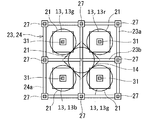
- first shield electrode 23 and the second shield electrode 24 will be described in detail.
- FIG. 5A is a plan view of the first pixel electrode 13 and the first shield electrode 23.
- FIG. 5B is a plan view of the second pixel electrode 14 and the second shield electrode 24.
- FIG. 5C is a plan view of the first pixel electrode 13, the first shield electrode 23, the second pixel electrode 14, and the second shield electrode 24.
- the first pixel electrode 13, the first shield electrode 23, the second pixel electrode 14, and the second shield electrode 24 show the positional relationship shown in FIG. 5C.
- the first shield electrode 23 has the shape of a frame surrounding the first pixel electrode 13.
- the charge collection efficiency is improved in all directions around the first pixel electrode 13.
- the second shield electrode 24 also has the shape of a frame surrounding the second pixel electrode 14.
- the charge collection efficiency is improved in all directions around the second pixel electrode 14. Improvement of charge collection efficiency leads to improvement of sensitivity.
- the first shield electrode 23 includes an outer peripheral portion 23a and a partition portion 23b.
- the outer peripheral portion 23a is a portion surrounding the four first pixel electrodes 13 belonging to the unit pixel 10.
- the outer peripheral portion 23a has the shape of a frame.
- the partition portion 23b is a portion that partitions the region surrounded by the outer peripheral portion 23a into four regions so that each of the first pixel electrodes 13 is individually surrounded by the first shield electrode 23. The areas of the four regions are equal to each other.
- the compartment 23b has a cross shape.
- the partition portion 23b is formed integrally with the outer peripheral portion 23a and is electrically connected to each other.
- the compartmentalized portion 23b of the first shield electrode 23 does not overlap the second shield electrode 24.
- the second shield electrode 24 includes an outer peripheral portion 24a.
- the outer peripheral portion has the shape of a frame.
- the second shield electrode 24 does not have a portion corresponding to the partition portion 23b of the first shield electrode 23.
- the design of the second shield electrode 24 is different from the design of the first shield electrode 23.
- the outer peripheral portion 24a of the second shield electrode 24 has the same design as the design of the outer peripheral portion 23a of the first shield electrode 23.
- FIG. 5C is a superposition of FIG. 5A and FIG. 5B.
- the outer peripheral portion 23a of the first shield electrode 23 overlaps with the second shield electrode 24.
- the first shield electrode 23 includes a line-shaped portion extending in the first direction D1 as its outer peripheral portion 23a.
- the second shield electrode 24 includes a line-shaped portion extending in the second direction D2 as its outer peripheral portion 24a.
- the first direction D1 and the second direction D2 are parallel to each other.
- the first direction D1 and the second direction D2 are, for example, the vertical directions in the arrangement direction of the unit pixels 10.
- the line-shaped portion of the first shield electrode 23 and the line-shaped portion of the second shield electrode 24 overlap each other.
- the at least one plug 27 includes a plurality of plugs 27 provided along the line-shaped portion of the first shield electrode 23 and the line-shaped portion of the second shield electrode 24. According to such a configuration, the shield resistance can be lowered more sufficiently.
- the second shield electrode 24 overlaps the first shield electrode 23 over 360 degrees around the second pixel electrode 14. Thereby, the above-mentioned effect can be more sufficiently obtained.
- the shortest distance between the first shield electrode 23 and the first pixel electrode 13 is different from the shortest distance between the second shield electrode 24 and the second pixel electrode 14.
- the shortest distance between the first shield electrode 23 and the first pixel electrode 13 is shorter than the shortest distance between the second shield electrode 24 and the second pixel electrode 14.
- the shortest distance between the first shield electrode 23 and the first pixel electrode 13 is, in detail, the shortest distance between the outer peripheral portion 23a of the first shield electrode 23 and the first pixel electrode 13, or the first shield electrode. It is the shortest distance between the partition portion 23b of 23 and the first pixel electrode 13.
- the sensitivity of the first pixel 10a (FIG. 2A) can be sufficiently improved.
- the charge collection efficiency can be improved over a wider range.
- the area M1 of the smallest region surrounded by the first shield electrode 23 is different from the area M2 of the smallest region surrounded by the second shield electrode 24.
- the area M1 of the former is smaller than the area M2 of the latter.
- the first shield electrode 23 and the second shield electrode 24 have a design suitable for each of the first pixel electrode 13 and the second pixel electrode 14. According to the example shown in FIGS. 5A to 5C, the ratio of the area M1 to the area M2 (M1 / M2) is about 1/4.
- the cross section of FIG. 2A may be a cross section along the straight line L shown in FIG. 5C.
- the first shield electrode 23 is located in the upper layer
- the second shield electrode 24 is located in the lower layer.
- FIG. 6 shows the planes of the first pixel electrode 13, the first shield electrode 23, the second pixel electrode 14, and the second shield electrode 24 when the second pixel array 104 is the upper layer and the first pixel array 102 is the lower layer. It is a figure.
- the resolution of the first pixel array 102 in the lower layer is high, and the resolution of the second pixel array 104 in the upper layer is low.
- the second plug 32 extends from the central region of the second pixel electrode 14 to the semiconductor substrate 1, and the partition portion 23b of the first shield electrode 23 is provided so as to avoid the second plug 32.
- FIG. 7 is a modified example of the example described with reference to FIGS. 5A to 5C.
- the diagonal direction of the second pixel electrode 14 is inclined by 45 degrees with respect to the diagonal direction of the first pixel electrode 13. This arrangement is the same as the arrangement described with reference to FIG. 4A.
- the area of the second pixel electrode 14 can be increased while reducing the overlap between the first pixel electrode 13 and the second pixel electrode 14.
- FIG. 8A to 8C show other modified examples.
- FIG. 8A is a plan view of the first pixel electrode 13 and the first shield electrode 23.
- FIG. 8B is a plan view of the second pixel electrode 14 and the second shield electrode 24.
- FIG. 8C is a plan view of the first pixel electrode 13, the first shield electrode 23, the second pixel electrode 14, and the second shield electrode 24.
- the design of the first shield electrode 23 is as described with reference to FIG. 5A. However, the position of the first plug 31 has been moved from the central region of the first pixel electrode 13 to the outer peripheral region.
- the second shield electrode 24 includes an outer peripheral portion 24a and a partition portion 24b.
- the outer peripheral portion 24a is a portion having the shape of a frame.
- the partition portion 24b is a portion that divides the region surrounded by the outer peripheral portion 24a into a plurality of regions. Specifically, the partition portion 24b has the shape of a rectangular frame and connects the midpoints of the four sides constituting the outer peripheral portion 24a.
- the partition portion 24b is formed integrally with the outer peripheral portion 24a and is electrically connected to each other.
- FIG. 8C is a superposition of FIG. 8A and FIG. 8B.
- the outer peripheral portion 23a of the first shield electrode 23 overlaps the outer peripheral portion 24a of the second shield electrode 24.
- the outer peripheral portion 23a has the same design as the outer peripheral portion 24a.
- the compartmentalized portion 23b of the first shield electrode 23 does not overlap the second shield electrode 24.
- the compartmentalized portion 24b of the second shield electrode 24 does not overlap the first shield electrode 23.
- each of the first shield electrode 23 and the second shield electrode 24 has a portion that does not overlap with each other.
- the first plug 31 is provided at a position that does not overlap with the compartmentalized portion 24b of the second shield electrode 24. According to such a configuration, it is possible to provide a shield electrode suitable for each of the first pixel electrode 13 and the second pixel electrode 14.
- the first plug 31 is located in a region different from the region in which the second pixel electrode 14 exists among the plurality of regions partitioned by the partition portion 24b.
- the partition portion 24b divides the region surrounded by the outer peripheral portion 24a into one rectangular region and four triangular regions.
- the second pixel electrode 14 exists in the rectangular area.
- the first plug 31 extends from the first pixel electrode 13 to the semiconductor substrate 1.
- the second photoelectric conversion layer 122 requires a via for penetrating the first plug 31.
- vias are formed by a process such as etching, damage due to lateral etching remains in the photoelectric conversion layer. The damage remaining in the photoelectric conversion layer causes a leakage current.
- the first plug 31 is surrounded by the second shield electrode 24 at the same level as the second pixel electrode 14. That is, the etched portion is surrounded by the second shield electrode 24. Since the etched portion is separated from the second pixel electrode 14 by the potential gradient generated by the second shield electrode 24, noise in the second pixel array 104 can be suppressed.
- the examples described with reference to FIGS. 8A to 8C are particularly effective when the low resolution pixel array is located in the lower layer and the high resolution pixel array is located in the upper layer.
- the shield between the first plug 31 and the second pixel electrode 14 is surely achieved, so that the coupling between the first plug 31 and the second pixel electrode 14 is further reduced. sell. As a result, further improvement in sensitivity can be expected.
- FIG. 9A is a plan view of the second pixel electrode 14 and the second shield electrode 24 in still another modified example.
- the second shield electrode 24 includes an outer peripheral portion 24a, a compartment portion 24b, and a plurality of subsection portions 24c.
- the outer peripheral portion 24a and the partition portion 24b are as described with reference to FIG. 8B.
- the subsection portion 24c has the shape of a rectangular frame.
- the small compartment portion 24c is provided in each of the four line-shaped portions constituting the compartment portion 24b, and surrounds the first plug 31.
- the outer peripheral portion 24a, the partition portion 24b, and the subsection portion 24c are integrally formed and are electrically connected to each other.
- FIG. 9B is a superposition of FIG. 5A and FIG. 9A.
- the outer peripheral portion 23a of the first shield electrode 23 overlaps the outer peripheral portion 24a of the second shield electrode 24.
- the outer peripheral portion 23a has the same design as the outer peripheral portion 24a.
- the compartmentalized portion 23b of the first shield electrode 23 does not overlap the second shield electrode 24.
- the compartmentalized portion 24b of the second shield electrode 24 does not overlap the first shield electrode 23.
- each of the first shield electrode 23 and the second shield electrode 24 has a portion that does not overlap with each other.
- the subdivision portion 24c of the second shield electrode 24 surrounds the first plug 31 and overlaps with the first shield electrode 23.
- the outer shape of the subdivision portion 24c may be contained inside the outer shape of the first shield electrode 23, or may match the outer shape of the first shield electrode 23. As long as the subdivision portion 24c does not contact the second pixel electrode 14, at least a part of the outer shape of the subpart portion 24c may be located outside the outer shape of the first shield electrode 23.
- the same effect as that described with reference to FIGS. 8A to 8C can be obtained. Since the shield between the first plug 31 and the second pixel electrode 14 is more reliably achieved, the coupling between the first plug 31 and the second pixel electrode 14 can be further reduced. As a result, further improvement in sensitivity can be expected.
- FIG. 10 is a plan view of the first pixel electrode 13, the first shield electrode 23, the second pixel electrode 14, and the second shield electrode 24 in still another modification.
- the ratio of the number of the second pixel electrodes 14 to the number of the first pixel electrodes 13 is equal.
- the outer peripheral portion 24a of the second shield electrode 24 surrounds the four second pixel electrodes 14.
- the design of the first shield electrode 23 and the second shield electrode 24 is as described with reference to FIGS. 5A and 5B.
- the diagonal direction of the outer peripheral portion 24a of the second shield electrode 24 is inclined by 45 degrees with respect to the diagonal direction of the outer peripheral portion 23a of the first shield electrode 23.
- the first shield electrode 23 includes a line-shaped portion extending in the first direction D1 as its outer peripheral portion 23a.
- the second shield electrode 24 includes a line-shaped portion extending in the second direction D2 as its outer peripheral portion 24a.
- the first direction D1 and the second direction D2 intersect each other.
- the first direction D1 is tilted 45 degrees with respect to the second direction D2.
- the overlap between the first shield electrode 23 and the second shield electrode 24 is minimized.
- the configuration shown in FIG. 10 is useful.
- the first shield electrode 23 may be electrically insulated from the second shield electrode 24.
- the voltage to be applied to the first shield electrode 23 may be different from the voltage to be applied to the second shield electrode 24.
- the characteristics of the first photoelectric conversion layer 121 are different from the characteristics of the second photoelectric conversion layer 122. Therefore, according to this modification, a voltage suitable for the first photoelectric conversion layer 121 is applied to the first shield electrode 23, and a voltage suitable for the second photoelectric conversion layer 122 is applied to the second shield electrode 24. Can be done. As a result, further improvement in charge collection efficiency can be expected.
- FIG. 11A is a plan view of the first pixel electrode 13, the first shield electrode 23, the second pixel electrode 14, and the second shield electrode 24 in still another modification.
- the upper view of FIG. 11A shows a set of the first pixel electrode 13 and the first shield electrode 23.
- the lower figure of FIG. 11A shows a set of the second pixel electrode 14 and the second shield electrode 24. These are stacked one above the other. In the example shown in FIG. 11A, the ratio of the number of the second pixel electrodes 14 to the number of the first pixel electrodes 13 is equal.
- the outer peripheral portion 24a of the second shield electrode 24 surrounds the four second pixel electrodes 14.
- the first pixel electrode 13 and the second pixel electrode 14 substantially overlap each other.
- the size of the second pixel electrode 14 is substantially the same as the size of the first pixel electrode 13, except that the second pixel electrode 14 is provided with a notch for passing the first plug 31. That is, the effect brought about by the first shield electrode 23 and the second shield electrode 24 is independent of the effect brought about by the offset between the first pixel electrode 13 and the second pixel electrode 14. Of course, with both configurations, the sensitivity is superposed.
- the compartmentalized portion 24b of the second shield electrode 24 has a cross shape. That is, the first shield electrode 23 and the second shield electrode 24 have the same design. Therefore, the overlap between the first shield electrode 23 and the second shield electrode 24 can be maximized.
- the second shield electrode 24 has the shape of a frame.
- the outer peripheral portion 24a may be composed of a plurality of line-shaped portions separated from each other.
- the partition portion 24b may be composed of a plurality of line-shaped portions separated from each other. The application of voltage to each part can be achieved through the plug. These configurations also apply to the first shield electrode 23.
- FIG. 12A to 12C show the arrangement of the condenser lens 21 in the unit pixel 10, respectively.
- the configurations of the first pixel electrode 13, the first shield electrode 23, the second pixel electrode 14, and the second shield electrode 24 correspond to the examples described with reference to FIG. 7.
- a condenser lens 21 is provided above each of the first pixel electrode 13 and above the second pixel electrode 14.
- the sensitivities of the first photoelectric conversion layer 121 and the second photoelectric conversion layer 122 can be improved.
- the condenser lens 21 may be provided only above each of the first pixel electrodes 13. Since the condenser lens is not provided above the second pixel electrode 14, it is possible to provide a condenser lens 21 having a large size above the first pixel electrode 13. In this case, the angle of incidence is widened and the sensitivity is also improved.
- FIG. 12C shows an example in which a dummy lens 22 is provided in addition to the condenser lens 21.
- the condenser lens 21 is provided above each of the first pixel electrode 13 and the second pixel electrode 14. There is no pixel electrode below the dummy lens 22.
- the dummy lens 22 is provided between the adjacent condensing lenses 21, the uniformity of the shape of the condensing lens 21 is improved.
- FIG. 13 shows a cross section of the image sensor 200 according to the second embodiment of the present disclosure.
- the color filter 190 corresponding to the second pixel electrode 14 is provided, and / or the condenser lens 21 is provided above the second pixel electrode 14.
- the image sensor 200 is different from the image sensors 100 and 110 described above.
- the color filter 190 includes a first filter 19r, a third filter 19b, and a second filter 19i.
- the first filter 19r is a filter that transmits red light.
- the third filter 19b is a filter that transmits blue light.
- the second filter 19i is a filter that transmits near-infrared light.
- a filter that transmits green light is arranged at a position (not shown) based on the Bayer arrangement.
- the wavelength range of red light is defined as the first wavelength range.
- the wavelength range of near-infrared light is defined as the second wavelength range.
- the wavelength range of blue light is defined as a third wavelength range different from the first wavelength range and the second wavelength range. Specifically, the central wavelength of the first wavelength region, the central wavelength of the second wavelength region, and the central wavelength of the third wavelength region are different from each other.
- the plurality of condenser lenses 21 include a first lens 21r, a third lens 21b, and a second lens 21i.
- the first lens 21r is a lens arranged above the first pixel electrode 13 that collects the electric charge generated by the red light.
- the third lens 21b is a lens arranged above the first pixel electrode 13 that collects the electric charge generated by the blue light.
- the second lens 21i is a lens arranged above the second pixel electrode 14 that collects the electric charges generated by the near infrared light.
- a lens is also arranged above the first pixel electrode 13 that collects the electric charge generated by the green light at a position (not shown).
- the shape of each lens may be the same or different.
- the material of each lens may be the same or different.
- FIG. 14A schematically shows the positional relationship between the filter and the pixel electrodes.
- the first filter 19r overlaps the first pixel electrode 13r
- the second filter 19i overlaps the second pixel electrode 14. According to such a configuration, it is possible to efficiently read out light of a specific wavelength as a signal while reducing the coupling capacitance between the first pixel electrode 13 and the second pixel electrode 14.
- a uniform color filter array can be realized, the yield is improved, and the color reproducibility is also improved.
- the third filter 19b overlaps the first pixel electrode 13b, which is different from the first pixel electrode 13r on which the first filter 19r overlaps. According to such a configuration, light in three different wavelength ranges can be efficiently read out as a signal while reducing the coupling capacitance between the pixel electrodes.
- FIG. 14B is another schematic view showing the positional relationship between the filter and the pixel electrodes.
- the example shown in FIG. 14B has the same arrangement as the example described with reference to FIG. 14A, except that the first pixel array 102 and the second pixel array 104 share a counter electrode 16.
- FIG. 15A schematically shows the positional relationship between the lens and the pixel electrode.
- the optical axis of the first lens 21r is located in the central region of the first pixel electrode 13r
- the optical axis of the second lens 21i is located in the central region of the second pixel electrode 14.
- the optical axis of the first lens 21r passes through the central region of the first pixel electrode 13r and deviates from the central region of the second pixel electrode 14.
- the optical axis of the second lens 21i passes through the central region of the second pixel electrode 14 and deviates from the central region of the first pixel electrode 13r.
- the optical axis of the third lens 21b is located in the central region of the first pixel electrode 13b, which is different from the first pixel electrode 13r in which the optical axis of the first lens 21r is located in the central region. According to such a configuration, light in three different wavelength ranges can be efficiently read out as a signal while reducing the coupling capacitance between the pixel electrodes.
- FIG. 15B is another schematic view showing the positional relationship between the lens and the pixel electrode.
- the example shown in FIG. 15B is the same as the example described with reference to FIG. 15A, except that the first pixel array 102 and the second pixel array 104 share the counter electrode 16.
- the second filter 19i may be omitted.
- only one condenser lens 21 is provided for one pixel electrode. This is advantageous for reducing the pixel pitch and enables high definition of the image sensor 200.
- the first photoelectric conversion layer 121 is made of a panchromatic material and the second photoelectric conversion layer 122 is made of a material sensitive to near-infrared light
- the first The condenser lens 21 may be provided only above the one-pixel electrode 13.
- a dedicated condensing lens is not provided above the second pixel electrode 14. According to such a configuration, high-sensitivity and high-resolution image formation suitable for human vision can be realized.
- the first shield electrode 23 and / or the second shield electrode 24 may be omitted from the image sensor 200.
- FIG. 16 is a cross-sectional view of the image sensor 300 according to another embodiment.
- the image pickup device 300 further includes a condenser lens 40.
- the condenser lens 40 is arranged between the first pixel array 102 and the second pixel array 104 and above the second pixel electrode 14 in the stacking direction. According to the condenser lens 40, more light collected by the condenser lens 21 can be guided to the second photoelectric conversion layer 122. As a result, the sensitivity of the second pixel 10b is improved.
- FIG. 17 is a cross-sectional view of the image sensor 400 according to still another embodiment.
- the image pickup device 400 further includes a waveguide structure 42.
- the waveguide structure 42 is arranged between the first pixel array 102 and the second pixel array 104 in the stacking direction. In plan view, the waveguide structure 42 is located around the second pixel electrode 14.
- the waveguide structure 42 is a structure configured to guide light in a specific direction by utilizing the difference in refractive index of the materials.
- the waveguide structure 42 can be made by combining silicon nitride and silicon dioxide. According to the waveguide structure 42, more light can be directed to the second photoelectric conversion layer 122. As a result, the sensitivity of the second pixel 10b is improved.
- the condenser lens 40 described with reference to FIG. 16 and the waveguide structure 42 described with reference to FIG. 17 can be appropriately adopted in other embodiments.
- FIG. 18 shows the configuration of the camera system 500.
- the camera system 500 includes an image pickup device 100A, a near-infrared light source 501, a lens 502, an ISP (Image Signal Processor) 503, a signal processing circuit 504, an edge processing circuit 505, and an edge processing circuit 506.
- the camera system 500 is configured to process data based on light in two wavelength ranges obtained by the image pickup apparatus 100A and output the data to the outside.
- Near-infrared light P1 is emitted from the near-infrared light source 501 toward the subject P2.
- the image pickup apparatus 100A receives the light P3 from the subject P2 through the lens 502.
- the image pickup apparatus 100A outputs data based on visible light and data based on near-infrared light in two systems. Data based on visible light is processed by ISP503. As a result, a full-color image can be obtained.
- the full-color image is transmitted to and displayed on the external display 509a.
- the full-color image is processed by the edge processing circuit 506 and then transmitted to the external device and / or the cloud 508a.
- the data based on near-infrared light is processed by the signal processing circuit 504.
- the signal processing circuit 504 may be configured to calculate the distance to the subject from the data based on the near infrared light.
- the image by the near infrared light is transmitted to the external display 509b and displayed.
- the image by the near infrared light is processed by the edge processing circuit 505 and then transmitted to the external device and / or the cloud 508a. It is also possible to add the full-color image and the image by near-infrared light and display them on the external display 509c.
- the techniques disclosed herein are useful for image sensors.
- the image pickup device can be applied to an image pickup device, an optical sensor, and the like.
- Examples of the imaging device include camera systems such as digital still cameras, medical cameras, surveillance cameras, in-vehicle cameras, digital single-lens reflex cameras, and digital mirrorless single-lens cameras.
Landscapes
- Engineering & Computer Science (AREA)
- Multimedia (AREA)
- Signal Processing (AREA)
- Physics & Mathematics (AREA)
- Spectroscopy & Molecular Physics (AREA)
- Solid State Image Pick-Up Elements (AREA)
Priority Applications (3)
| Application Number | Priority Date | Filing Date | Title |
|---|---|---|---|
| CN202080070972.1A CN114556572A (zh) | 2019-10-30 | 2020-09-28 | 摄像元件 |
| JP2021554193A JPWO2021084994A1 (https=) | 2019-10-30 | 2020-09-28 | |
| US17/705,224 US20220217294A1 (en) | 2019-10-30 | 2022-03-25 | Imaging device |
Applications Claiming Priority (2)
| Application Number | Priority Date | Filing Date | Title |
|---|---|---|---|
| JP2019-197384 | 2019-10-30 | ||
| JP2019197384 | 2019-10-30 |
Related Child Applications (1)
| Application Number | Title | Priority Date | Filing Date |
|---|---|---|---|
| US17/705,224 Continuation US20220217294A1 (en) | 2019-10-30 | 2022-03-25 | Imaging device |
Publications (1)
| Publication Number | Publication Date |
|---|---|
| WO2021084994A1 true WO2021084994A1 (ja) | 2021-05-06 |
Family
ID=75715079
Family Applications (1)
| Application Number | Title | Priority Date | Filing Date |
|---|---|---|---|
| PCT/JP2020/036495 Ceased WO2021084994A1 (ja) | 2019-10-30 | 2020-09-28 | 撮像素子 |
Country Status (4)
| Country | Link |
|---|---|
| US (1) | US20220217294A1 (https=) |
| JP (1) | JPWO2021084994A1 (https=) |
| CN (1) | CN114556572A (https=) |
| WO (1) | WO2021084994A1 (https=) |
Cited By (3)
| Publication number | Priority date | Publication date | Assignee | Title |
|---|---|---|---|---|
| US20240302709A1 (en) * | 2021-02-01 | 2024-09-12 | Northwestern University | Wavelength converting natural vision system |
| WO2025088923A1 (ja) * | 2023-10-26 | 2025-05-01 | パナソニックIpマネジメント株式会社 | 撮像装置およびカメラシステム |
| WO2025197482A1 (ja) * | 2024-03-19 | 2025-09-25 | パナソニックIpマネジメント株式会社 | 撮像装置及びカメラシステム |
Citations (13)
| Publication number | Priority date | Publication date | Assignee | Title |
|---|---|---|---|---|
| JPH03148175A (ja) * | 1989-11-02 | 1991-06-24 | Fujitsu Ltd | 赤外線検知装置 |
| JPH0513741A (ja) * | 1991-06-28 | 1993-01-22 | Yokogawa Electric Corp | 半導体光検出装置 |
| JP2005353626A (ja) * | 2004-06-08 | 2005-12-22 | Fuji Photo Film Co Ltd | 光電変換膜積層型固体撮像素子及びその製造方法 |
| JP2009054806A (ja) * | 2007-08-27 | 2009-03-12 | Canon Inc | 撮像素子及び撮像装置 |
| JP2011187725A (ja) * | 2010-03-09 | 2011-09-22 | Toshiba Corp | 固体撮像装置 |
| JP2012104759A (ja) * | 2010-11-12 | 2012-05-31 | Fujitsu Ltd | 赤外線イメージセンサ及び赤外線撮像装置 |
| JP2015073070A (ja) * | 2013-10-02 | 2015-04-16 | 采▲ぎょく▼科技股▲ふん▼有限公司VisEra Technologies Company Limited | 光電変換層の隔壁を有する撮像装置 |
| WO2016002576A1 (ja) * | 2014-07-03 | 2016-01-07 | ソニー株式会社 | 固体撮像素子、および電子装置 |
| JP2016012642A (ja) * | 2014-06-27 | 2016-01-21 | パナソニックIpマネジメント株式会社 | 固体撮像装置及びその制御方法 |
| JP2016152417A (ja) * | 2015-02-16 | 2016-08-22 | 三星電子株式会社Samsung Electronics Co.,Ltd. | イメージセンサ、及びイメージセンサを含む撮像装置 |
| KR20180040556A (ko) * | 2018-04-13 | 2018-04-20 | 삼성전자주식회사 | 유기 광전 변환부를 채용한 이미지 센서 |
| US20180190697A1 (en) * | 2017-01-03 | 2018-07-05 | Samsung Electronics Co., Ltd. | Image sensor |
| JP2018160779A (ja) * | 2017-03-22 | 2018-10-11 | キヤノン株式会社 | 撮像素子及びその制御方法、撮像装置、焦点検出装置及び方法 |
Family Cites Families (9)
| Publication number | Priority date | Publication date | Assignee | Title |
|---|---|---|---|---|
| JP2007066962A (ja) * | 2005-08-29 | 2007-03-15 | Fujifilm Corp | カラー固体撮像装置及びデジタルカメラ |
| WO2011055638A1 (en) * | 2009-11-06 | 2011-05-12 | Semiconductor Energy Laboratory Co., Ltd. | Display device |
| JP6079502B2 (ja) * | 2013-08-19 | 2017-02-15 | ソニー株式会社 | 固体撮像素子および電子機器 |
| TWI505455B (zh) * | 2013-09-27 | 2015-10-21 | Maxchip Electronics Corp | 光感測器 |
| KR20150123088A (ko) * | 2014-04-24 | 2015-11-03 | 삼성전자주식회사 | 스큐드 픽셀 구조를 갖는 이미지 센서를 포함하는 이미지 데이터 처리 장치 |
| US9967501B2 (en) * | 2014-10-08 | 2018-05-08 | Panasonic Intellectual Property Management Co., Ltd. | Imaging device |
| CN111968998B (zh) * | 2014-12-26 | 2024-12-13 | 松下知识产权经营株式会社 | 摄像装置 |
| KR102701853B1 (ko) * | 2015-12-14 | 2024-09-02 | 삼성전자주식회사 | 이미지 센서 |
| DE102015225797B3 (de) * | 2015-12-17 | 2017-05-04 | Robert Bosch Gmbh | Optischer Detektor |
-
2020
- 2020-09-28 JP JP2021554193A patent/JPWO2021084994A1/ja active Pending
- 2020-09-28 WO PCT/JP2020/036495 patent/WO2021084994A1/ja not_active Ceased
- 2020-09-28 CN CN202080070972.1A patent/CN114556572A/zh active Pending
-
2022
- 2022-03-25 US US17/705,224 patent/US20220217294A1/en not_active Abandoned
Patent Citations (13)
| Publication number | Priority date | Publication date | Assignee | Title |
|---|---|---|---|---|
| JPH03148175A (ja) * | 1989-11-02 | 1991-06-24 | Fujitsu Ltd | 赤外線検知装置 |
| JPH0513741A (ja) * | 1991-06-28 | 1993-01-22 | Yokogawa Electric Corp | 半導体光検出装置 |
| JP2005353626A (ja) * | 2004-06-08 | 2005-12-22 | Fuji Photo Film Co Ltd | 光電変換膜積層型固体撮像素子及びその製造方法 |
| JP2009054806A (ja) * | 2007-08-27 | 2009-03-12 | Canon Inc | 撮像素子及び撮像装置 |
| JP2011187725A (ja) * | 2010-03-09 | 2011-09-22 | Toshiba Corp | 固体撮像装置 |
| JP2012104759A (ja) * | 2010-11-12 | 2012-05-31 | Fujitsu Ltd | 赤外線イメージセンサ及び赤外線撮像装置 |
| JP2015073070A (ja) * | 2013-10-02 | 2015-04-16 | 采▲ぎょく▼科技股▲ふん▼有限公司VisEra Technologies Company Limited | 光電変換層の隔壁を有する撮像装置 |
| JP2016012642A (ja) * | 2014-06-27 | 2016-01-21 | パナソニックIpマネジメント株式会社 | 固体撮像装置及びその制御方法 |
| WO2016002576A1 (ja) * | 2014-07-03 | 2016-01-07 | ソニー株式会社 | 固体撮像素子、および電子装置 |
| JP2016152417A (ja) * | 2015-02-16 | 2016-08-22 | 三星電子株式会社Samsung Electronics Co.,Ltd. | イメージセンサ、及びイメージセンサを含む撮像装置 |
| US20180190697A1 (en) * | 2017-01-03 | 2018-07-05 | Samsung Electronics Co., Ltd. | Image sensor |
| JP2018160779A (ja) * | 2017-03-22 | 2018-10-11 | キヤノン株式会社 | 撮像素子及びその制御方法、撮像装置、焦点検出装置及び方法 |
| KR20180040556A (ko) * | 2018-04-13 | 2018-04-20 | 삼성전자주식회사 | 유기 광전 변환부를 채용한 이미지 센서 |
Cited By (3)
| Publication number | Priority date | Publication date | Assignee | Title |
|---|---|---|---|---|
| US20240302709A1 (en) * | 2021-02-01 | 2024-09-12 | Northwestern University | Wavelength converting natural vision system |
| WO2025088923A1 (ja) * | 2023-10-26 | 2025-05-01 | パナソニックIpマネジメント株式会社 | 撮像装置およびカメラシステム |
| WO2025197482A1 (ja) * | 2024-03-19 | 2025-09-25 | パナソニックIpマネジメント株式会社 | 撮像装置及びカメラシステム |
Also Published As
| Publication number | Publication date |
|---|---|
| US20220217294A1 (en) | 2022-07-07 |
| JPWO2021084994A1 (https=) | 2021-05-06 |
| CN114556572A (zh) | 2022-05-27 |
Similar Documents
| Publication | Publication Date | Title |
|---|---|---|
| US10818713B2 (en) | Solid-state imaging device and electronic apparatus including a photoelectric conversion unit disposed between another photoelectric conversion unit and a photoelectric conversion film | |
| US10559616B2 (en) | Solid-state imaging apparatus and electronic device | |
| US10566557B2 (en) | Solid-state imaging element, production method thereof, and electronic device | |
| JP6879919B2 (ja) | 固体撮像素子、電子機器、及び、固体撮像素子の製造方法 | |
| US20190043911A1 (en) | Imaging device | |
| US20220217294A1 (en) | Imaging device | |
| JP6555867B2 (ja) | 撮像装置 | |
| US20220028918A1 (en) | Imaging device | |
| US20210408099A1 (en) | Imaging device | |
| JP2009147147A (ja) | 有機光電変換素子 | |
| WO2021084995A1 (ja) | 撮像素子 | |
| WO2020218047A1 (ja) | 撮像素子 | |
| CN110098218B (zh) | 摄像装置 | |
| US20140110771A1 (en) | Solid-state imaging device and semiconductor device | |
| US12302652B2 (en) | Imaging device | |
| WO2025182236A1 (ja) | 撮像装置およびカメラシステム | |
| WO2022033242A1 (zh) | 感测基板和电子装置 | |
| JPH0462872A (ja) | 固体撮像装置 |
Legal Events
| Date | Code | Title | Description |
|---|---|---|---|
| 121 | Ep: the epo has been informed by wipo that ep was designated in this application |
Ref document number: 20882550 Country of ref document: EP Kind code of ref document: A1 |
|
| ENP | Entry into the national phase |
Ref document number: 2021554193 Country of ref document: JP Kind code of ref document: A |
|
| NENP | Non-entry into the national phase |
Ref country code: DE |
|
| 122 | Ep: pct application non-entry in european phase |
Ref document number: 20882550 Country of ref document: EP Kind code of ref document: A1 |