WO2021065829A1 - 透明導電性フィルムの製造方法 - Google Patents
透明導電性フィルムの製造方法 Download PDFInfo
- Publication number
- WO2021065829A1 WO2021065829A1 PCT/JP2020/036699 JP2020036699W WO2021065829A1 WO 2021065829 A1 WO2021065829 A1 WO 2021065829A1 JP 2020036699 W JP2020036699 W JP 2020036699W WO 2021065829 A1 WO2021065829 A1 WO 2021065829A1
- Authority
- WO
- WIPO (PCT)
- Prior art keywords
- transparent conductive
- blowing
- conductive film
- coating layer
- base material
- Prior art date
- Legal status (The legal status is an assumption and is not a legal conclusion. Google has not performed a legal analysis and makes no representation as to the accuracy of the status listed.)
- Ceased
Links
Images

Classifications
-
- B—PERFORMING OPERATIONS; TRANSPORTING
- B05—SPRAYING OR ATOMISING IN GENERAL; APPLYING FLUENT MATERIALS TO SURFACES, IN GENERAL
- B05D—PROCESSES FOR APPLYING FLUENT MATERIALS TO SURFACES, IN GENERAL
- B05D3/00—Pretreatment of surfaces to which liquids or other fluent materials are to be applied; After-treatment of applied coatings, e.g. intermediate treating of an applied coating preparatory to subsequent applications of liquids or other fluent materials
- B05D3/04—Pretreatment of surfaces to which liquids or other fluent materials are to be applied; After-treatment of applied coatings, e.g. intermediate treating of an applied coating preparatory to subsequent applications of liquids or other fluent materials by exposure to gases
-
- H—ELECTRICITY
- H01—ELECTRIC ELEMENTS
- H01B—CABLES; CONDUCTORS; INSULATORS; SELECTION OF MATERIALS FOR THEIR CONDUCTIVE, INSULATING OR DIELECTRIC PROPERTIES
- H01B13/00—Apparatus or processes specially adapted for manufacturing conductors or cables
- H01B13/30—Drying; Impregnating
-
- B—PERFORMING OPERATIONS; TRANSPORTING
- B05—SPRAYING OR ATOMISING IN GENERAL; APPLYING FLUENT MATERIALS TO SURFACES, IN GENERAL
- B05D—PROCESSES FOR APPLYING FLUENT MATERIALS TO SURFACES, IN GENERAL
- B05D3/00—Pretreatment of surfaces to which liquids or other fluent materials are to be applied; After-treatment of applied coatings, e.g. intermediate treating of an applied coating preparatory to subsequent applications of liquids or other fluent materials
-
- B—PERFORMING OPERATIONS; TRANSPORTING
- B05—SPRAYING OR ATOMISING IN GENERAL; APPLYING FLUENT MATERIALS TO SURFACES, IN GENERAL
- B05D—PROCESSES FOR APPLYING FLUENT MATERIALS TO SURFACES, IN GENERAL
- B05D5/00—Processes for applying liquids or other fluent materials to surfaces to obtain special surface effects, finishes or structures
- B05D5/06—Processes for applying liquids or other fluent materials to surfaces to obtain special surface effects, finishes or structures to obtain multicolour or other optical effects
-
- B—PERFORMING OPERATIONS; TRANSPORTING
- B05—SPRAYING OR ATOMISING IN GENERAL; APPLYING FLUENT MATERIALS TO SURFACES, IN GENERAL
- B05D—PROCESSES FOR APPLYING FLUENT MATERIALS TO SURFACES, IN GENERAL
- B05D5/00—Processes for applying liquids or other fluent materials to surfaces to obtain special surface effects, finishes or structures
- B05D5/12—Processes for applying liquids or other fluent materials to surfaces to obtain special surface effects, finishes or structures to obtain a coating with specific electrical properties
-
- B—PERFORMING OPERATIONS; TRANSPORTING
- B05—SPRAYING OR ATOMISING IN GENERAL; APPLYING FLUENT MATERIALS TO SURFACES, IN GENERAL
- B05D—PROCESSES FOR APPLYING FLUENT MATERIALS TO SURFACES, IN GENERAL
- B05D7/00—Processes, other than flocking, specially adapted for applying liquids or other fluent materials to particular surfaces or for applying particular liquids or other fluent materials
-
- B—PERFORMING OPERATIONS; TRANSPORTING
- B05—SPRAYING OR ATOMISING IN GENERAL; APPLYING FLUENT MATERIALS TO SURFACES, IN GENERAL
- B05D—PROCESSES FOR APPLYING FLUENT MATERIALS TO SURFACES, IN GENERAL
- B05D7/00—Processes, other than flocking, specially adapted for applying liquids or other fluent materials to particular surfaces or for applying particular liquids or other fluent materials
- B05D7/24—Processes, other than flocking, specially adapted for applying liquids or other fluent materials to particular surfaces or for applying particular liquids or other fluent materials for applying particular liquids or other fluent materials
-
- H—ELECTRICITY
- H01—ELECTRIC ELEMENTS
- H01B—CABLES; CONDUCTORS; INSULATORS; SELECTION OF MATERIALS FOR THEIR CONDUCTIVE, INSULATING OR DIELECTRIC PROPERTIES
- H01B13/00—Apparatus or processes specially adapted for manufacturing conductors or cables
-
- H—ELECTRICITY
- H01—ELECTRIC ELEMENTS
- H01B—CABLES; CONDUCTORS; INSULATORS; SELECTION OF MATERIALS FOR THEIR CONDUCTIVE, INSULATING OR DIELECTRIC PROPERTIES
- H01B5/00—Non-insulated conductors or conductive bodies characterised by their form
- H01B5/14—Non-insulated conductors or conductive bodies characterised by their form comprising conductive layers or films on insulating-supports
Definitions
- the present invention relates to a method for producing a transparent conductive film.
- a transparent conductive film obtained by forming a metal oxide layer such as ITO (indium-tin composite oxide) on a transparent resin film is often used as an electrode of the touch sensor.
- the transparent conductive film provided with this metal oxide layer tends to lose its conductivity due to bending, and has a problem that it is difficult to use in applications requiring flexibility such as a flexible display.
- a transparent conductive film having high flexibility a transparent conductive film containing metal nanowires is known.
- Metal nanowires are wire-like conductive substances having a diameter of nanometers.
- the metal nanowires form a mesh, so that a good electrical conduction path is formed with a small amount of metal nanowires, and an opening is formed in the gap between the meshes. Formed to achieve high light transmittance.
- the metal nanowires are in the form of wires, they are likely to be arranged in an oriented state, and therefore, there is a problem that conductive anisotropy occurs in the transparent conductive film containing the metal nanowires.
- the present invention has been made to solve the above problems, and an object of the present invention is to provide a method for producing a transparent conductive film having a small conductive anisotropy while containing metal nanowires. is there.
- the method for producing a transparent conductive film of the present invention is a method for producing a transparent conductive film including a base material and a transparent conductive layer arranged on one side of the base material, wherein the long base material is formed. It includes a coating step of applying a composition for forming a transparent conductive layer containing metal nanowires to the base material to form a coating layer while transporting, and a blowing step of blowing air from above the coating layer.
- the blast in the blast step includes blast in a direction substantially perpendicular to the coating layer surface.
- the blowing in the blowing step includes blowing in an oblique direction with respect to the coating layer surface.
- the blower in the blower step is a spiral blower.
- a transparent conductive film is provided. This transparent conductive film is manufactured by the above manufacturing method.
- FIGS. 1-10 are schematic front views explaining the blowing direction in the blowing process in one embodiment of the present invention. It is the schematic sectional drawing of the transparent conductive film obtained by the manufacturing method by one Embodiment of this invention.
- A. Outline of Method for Producing Transparent Conductive Film In the method for producing a transparent conductive film of the present invention, a composition for forming a transparent conductive layer containing a metal nanowire is applied to the base material while transporting a long base material.
- the coating step of forming the coating layer and the blowing step of blowing air from above the coating layer (opposite to the base material of the coating layer) are included.
- a transparent conductive film including a base material and a transparent conductive layer arranged on one side of the base material can be obtained.
- the production method of the present invention may include any suitable other steps in addition to the above-mentioned coating step and blowing step.
- the manufacturing method may further include a drying step of drying the coating layer after the blowing step.
- the blowing step is a step in which the coating layer can be dried, and the transparent conductive layer is formed through the blowing step.
- the coating step and the blowing step are performed while feeding the rolled base material and transporting the base material to obtain the base material.
- a long transparent conductive film including a transparent conductive layer arranged on one side of the base material is formed.
- the transparent conductive film is wound up after formation.
- FIGS. 1A to 1C are schematic front views (viewed from the transparent conductive film winding side) for explaining the blowing direction in the blowing step in one embodiment of the present invention.
- FIGS. 1A to 1C the state of blowing air as seen from the side surface of the base material 10 on which the coating layer 21 is formed is shown.
- the blowing in the blowing step includes blowing in a direction substantially perpendicular to the 21 surface of the coating layer.
- substantially vertical means that the angle between the two directions is 80 ° to 100 °.
- the angle between the blowing direction Z and the 21 surface of the coating layer in the blowing step is preferably 85 ° to 95 °, more preferably 87 ° to 93 °.
- the blowing in the blowing step includes blowing in an oblique direction with respect to the 21 surface of the coating layer.
- the oblique direction means that the angle formed by the two directions is 20 ° or more and less than 80 ° or more than 100 ° and 160 ° or less.
- the angle between the blowing direction Z and the 21 surface of the coating layer in the blowing step is preferably 30 ° or more and less than 80 °, or more than 100 ° and 150 ° or less, and more preferably 45 ° to 75 °. Or 105 ° to 135 °. It should be noted that a combination of air blown in a substantially vertical direction and air blown in an oblique direction may be combined, and for example, air may be blown in a conical shape or a fan shape.
- the blowing direction seen from the coating layer surface side may or may not be parallel to the transport direction A of the base material.
- the angle formed by the blowing direction and the transport direction A of the base material when viewed from the coating layer surface side is preferably 0 ° to 60 °, more preferably 0 ° to 45 °, and even more preferably 0 ° to 0 °. It is 30 °.
- Examples of the embodiment in which the air is blown from above the coating layer (opposite to the base material of the coating layer) include the embodiments shown in FIGS. 1 (a) and 1 (b) and as shown in FIG. 1 (c).
- An embodiment in which the wind is blown in a spiral shape (that is, the wind is blown as a spiral flow) can also be mentioned.
- the wind blowing in a substantially fixed direction rather than in a spiral shape like the wind shown in FIGS. 1A and 1B is referred to as a rectifying wind.
- the direction Z'of the spiral axis of the wind as seen from the side surface side of the base material 10 may be a direction substantially perpendicular to the surface of the coating layer 21 or an oblique direction. You may.
- a spiral stream air is blown to the coating layer 21 surface in a direction in which the direction Z'of the spiral axis is substantially perpendicular to the coating layer 21 surface.
- the angle between the spiral axial direction Z'of the wind and the 21 surface of the coating layer in the blowing step is preferably 85 ° to 95 °, more preferably 87 ° to 93 °.
- the angle between the wind spiral axis direction Z'and the coating layer 21 surface in the blowing process is preferably 30 ° or more and 80 It is less than ° or more than 100 ° and 150 ° or less, more preferably 45 ° to 75 ° or 105 ° to 135 °.
- the direction of the wind spiral axis seen from the coating layer surface side may or may not be parallel to the transport direction A of the base material.
- the angle formed by the direction of the spiral axis of the wind and the transport direction A of the base material when viewed from the coating layer surface side is preferably 0 ° to 60 °, more preferably 0 ° to 45 °, and even more preferably. Is 0 ° to 30 °.
- the present invention by setting the wind direction in the blowing process to a specific direction, the orientation of the metal nanowires is disturbed, and as a result, a transparent conductive film having a small conductive anisotropy can be produced. Further, by blowing air from above the coating layer surface, the metal nanowires can be localized and densely present on the base material side in the coating layer, and the contact between the metal nanowires increases. As a result, a transparent conductive film having excellent conductivity can be obtained.
- the composition for forming a transparent conductive layer containing metal nanowires is applied to the substrate while transporting the elongated substrate to form the coating layer.
- Base material Any suitable material can be used as the material constituting the base material. Specifically, for example, a polymer base material such as a film or a plastic base material is preferably used. This is because the smoothness of the base material and the wettability to the composition for forming the transparent conductive layer are excellent, and the productivity can be significantly improved by the continuous production by the roll.
- the material constituting the above base material is typically a polymer film containing a thermoplastic resin as a main component.
- the thermoplastic resin include polyester resins; cycloolefin resins such as polynorbornene; acrylic resins; polycarbonate resins; cellulose resins and the like. Of these, polyester-based resins, cycloolefin-based resins, and acrylic-based resins are preferable. These resins are excellent in transparency, mechanical strength, thermal stability, moisture shielding property and the like.
- the above-mentioned thermoplastic resin may be used alone or in combination of two or more kinds. Further, it is also possible to use an optical film such as that used for a polarizing plate, for example, a low retardation base material, a high retardation base material, a retardation plate, a brightness improving film, or the like as a base material.
- the thickness of the base material is preferably 20 ⁇ m to 200 ⁇ m, more preferably 30 ⁇ m to 150 ⁇ m.
- the total light transmittance of the base material is preferably 30% or more, more preferably 35% or more, and further preferably 40% or more.
- Any appropriate method can be adopted as the method for transporting the base material.
- transport by a transport roll, transport by a transport belt, a combination thereof, and the like can be mentioned.
- the transport speed is, for example, 5 m / min to 50 m / min.
- Metal nanowires are conductive substances that are made of metal, have a needle-like or thread-like shape, and have a diameter of nanometers.
- the metal nanowires may be linear or curved. If a transparent conductive layer made of metal nanowires is used, the metal nanowires have a mesh shape, so that a good electric conduction path can be formed even with a small amount of metal nanowires, and the transparent material has low electric resistance. A conductive film can be obtained. Further, since the metal nanowires have a mesh shape, an opening can be formed in the gap between the meshes to obtain a transparent conductive film having high light transmittance.
- the ratio (aspect ratio: L / d) of the thickness d to the length L of the metal nanowire is preferably 100 to 100,000, more preferably 50 to 100,000, and particularly preferably 100 to 100. It is 10,000.
- the metal nanowires having such a large aspect ratio are used, the metal nanowires can intersect well and a small amount of metal nanowires can exhibit high conductivity. As a result, a transparent conductive film having high light transmittance can be obtained.
- the "thickness of the metal nanowire” means the diameter of the metal nanowire when it has a circular cross section, and means its minor diameter when it has an elliptical cross section, and is polygonal. In some cases it means the longest diagonal.
- the thickness and length of the metal nanowires can be confirmed by a scanning electron microscope or a transmission electron microscope.
- the thickness of the metal nanowires is preferably less than 500 nm, more preferably less than 200 nm, particularly preferably 10 nm to 100 nm, and most preferably 10 nm to 50 nm. Within such a range, a transparent conductive layer having high light transmittance can be formed.
- the length of the metal nanowires is preferably 1 ⁇ m to 1000 ⁇ m, more preferably 10 ⁇ m to 500 ⁇ m, and particularly preferably 10 ⁇ m to 100 ⁇ m. Within such a range, a transparent conductive film having high conductivity can be obtained.
- any suitable metal can be used as long as it is a conductive metal.
- the metal constituting the metal nanowire include silver, gold, copper, nickel and the like. Further, a material obtained by plating (for example, gold plating) these metals may be used. Of these, silver, copper or gold is preferable, and silver is more preferable, from the viewpoint of conductivity.
- any appropriate method can be adopted as the method for producing the metal nanowires.
- Examples thereof include a method of reducing silver nitrate in a solution, a method of applying an applied voltage or a current to the surface of the precursor from the tip of the probe, pulling out a metal nanowire at the tip of the probe, and continuously forming the metal nanowire. ..
- silver nanowires can be synthesized by liquid-phase reducing a silver salt such as silver nitrate in the presence of a polyol such as ethylene glycol and polyvinylpyrrolidone. Uniform size silver nanowires are available, for example, from Xia, Y. et al. etal. , Chem. Mater. (2002), 14, 4736-4745, Xia, Y. et al. etal. , Nano letters (2003) 3 (7), 955-960, can be mass-produced according to the method described.
- composition for forming a transparent conductive layer contains metal nanowires.
- metal nanowires are dispersed in any suitable solvent to prepare a composition for forming a transparent conductive layer.
- the solvent include water, alcohol solvents, ketone solvents, ether solvents, hydrocarbon solvents, aromatic solvents and the like.
- the composition for forming a transparent conductive layer may further contain additives such as a resin (binder resin), a conductive material other than metal nanowires (for example, conductive particles), and a leveling agent.
- the composition for forming a transparent conductive layer includes a plasticizer, a heat stabilizer, a light stabilizer, a lubricant, an antioxidant, an ultraviolet absorber, a flame retardant, a colorant, an antistatic agent, a compatibilizer, a cross-linking agent, and an increase. It may contain additives such as thickeners, inorganic particles, surfactants, and dispersants.
- the viscosity of the composition for forming the transparent conductive layer is preferably 5 mP ⁇ s / 25 ° C. to 300 mP ⁇ s / 25 ° C., more preferably 10 mP ⁇ s / 25 ° C. to 100 mP ⁇ s / 25 ° C. Within such a range, the effect obtained by setting the wind direction in the blowing process to a specific direction becomes large.
- the viscosity of the composition for forming a transparent conductive layer can be measured with a rheometer (for example, MCR302 manufactured by Anton Pearl Co., Ltd.).
- the dispersion concentration of the metal nanowires in the composition for forming the transparent conductive layer is preferably 0.01% by weight to 5% by weight. Within such a range, the effect of the present invention becomes remarkable.
- any appropriate method can be adopted as the method for applying the composition for forming the transparent conductive layer.
- the coating method include spray coating, bar coating, roll coating, die coating, inkjet coating, screen coating, dip coating, letterpress printing method, intaglio printing method, gravure printing method and the like.
- the basis weight of the coating layer is preferably 0.3 g / m 2 to 30 g / m 2 , and more preferably 1.6 g / m 2 to 16 g / m 2 .
- the metal nanowires can be satisfactorily dispersed by the blowing in the blowing step, and a transparent conductive film having a smaller conductive anisotropy can be produced.
- the film thickness of the coating layer is preferably 1 ⁇ m to 50 ⁇ m, and more preferably 2 ⁇ m to 40 ⁇ m.
- blower step As described above, in the blower step, the metal nanowires in the coating layer are oriented by blowing air to the coating layer side.
- the direction of ventilation is as described in Section A.
- Blower to the coating layer can be performed by any appropriate method.
- a blower located above the coating layer (opposite the substrate) can be used to blow air to the coating layer.
- the blowing direction can be adjusted by, for example, providing a louver in the blower and adjusting the blowing direction according to the direction of the louver.
- the blowing direction is defined by the opening direction of the louver.
- a blower having a spiral wind direction plate at the air outlet can be used.
- the wind speed of the above wind is preferably 0.5 m / s to 10 m / s, and more preferably 1 m / s to 7 m / s.
- the metal nanowires are satisfactorily dispersed in the vicinity of the base material, and a transparent conductive film having excellent conductivity and smaller conductive anisotropy can be produced.
- a transparent conductive film having excellent surface smoothness and thickness uniformity can be obtained.
- the wind speed can be appropriately set depending on the solvent and the like contained in the composition for forming the transparent conductive layer.
- the wind speed is preferably 0.5 m / s to 10 m / s, more preferably 1 m / s to 7 m / s.
- the wind speed means the wind speed at the time of reaching the coating layer.
- the temperature of the wind is preferably 10 ° C to 50 ° C, more preferably 15 ° C to 30 ° C.
- the wind speed can be appropriately set depending on the solvent and the like contained in the composition for forming the transparent conductive layer.
- the temperature of the wind is preferably 10 ° C. to 50 ° C., more preferably 15 ° C. to 30 ° C.
- the wind temperature means the temperature of the wind at the time of reaching the coating layer.
- the blowing time is preferably 1 minute to 10 minutes, more preferably 2 minutes to 5 minutes.
- the metal nanowires are well dispersed, and a transparent conductive film having a smaller conductive anisotropy can be produced.
- the metal nanowires can be appropriately dispersed over the entire coating layer, and a transparent conductive film having a smaller conductive anisotropy can be obtained.
- a transparent conductive film having excellent surface smoothness and thickness uniformity can be obtained.
- the above air is blown to the base material (the base material on which the coating layer is formed) on the transport roll.
- the metal nanowires are well dispersed, and a transparent conductive film having a smaller conductive anisotropy can be produced.
- a transparent conductive film having excellent surface smoothness and thickness uniformity can be obtained.
- the blowing may be divided into a plurality of stages.
- the wind may be divided into zones so that the wind direction, the wind speed, the temperature, and the like are different, and the air is blown stepwise.
- the thickness of the coating layer may be reduced by a method such as oven heating or natural drying before the blowing step.
- Basis weight of the coating layer at the start of air blowing process is preferably 0.001g / m 2 ⁇ 0.09g / m 2, more preferably 0.005g / m 2 ⁇ 0.05g / m 2.
- any appropriate treatment may be performed.
- a composition for forming a transparent conductive layer containing a binder resin it may be cured by irradiation with ultraviolet rays or the like.
- a drying step may be performed after the sending step. Examples of the drying method include oven heating, natural drying and the like.
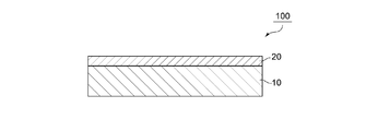
- FIG. 2 is a schematic cross-sectional view of a transparent conductive film obtained by the production method according to one embodiment of the present invention.
- the transparent conductive film 100 includes a base material 10 and a transparent conductive layer 20 arranged on one side of the base material 10.
- the surface resistance value of the transparent conductive film is preferably 0.1 ⁇ / ⁇ to 1000 ⁇ / ⁇ , more preferably 0.5 ⁇ / ⁇ to 300 ⁇ / ⁇ , and particularly preferably 1 ⁇ / ⁇ to 200 ⁇ / ⁇ . is there.
- the ratio (TD / MD) of the surface resistance value in TD (direction orthogonal to MD) to the surface resistance value in MD (conveyance direction) of the transparent conductive film is preferably 0.7 to 1.5, and more. It is preferably 0.8 to 1.2, and more preferably 0.9 to 1.1.
- the surface resistance value can be measured by "Automatic resistivity measurement system MCP-S620 type / MCP-S521 type" manufactured by Mitsubishi Chemical Analytech.
- the haze value of the transparent conductive film is preferably 20% or less, more preferably 10% or less, and further preferably 0.1% to 5%.
- the total light transmittance of the transparent conductive film is preferably 30% or more, more preferably 35% or more, and particularly preferably 40% or more.
- Basis weight of the transparent conductive layer is preferably 0.001g / m 2 ⁇ 0.09g / m 2, more preferably 0.005g / m 2 ⁇ 0.05g / m 2.
- the content ratio of the metal nanowires in the transparent conductive layer is preferably 0.1 parts by weight to 50 parts by weight, more preferably 0.1 parts by weight or more, based on 100 parts by weight of the binder resin constituting the transparent conductive layer. It is 30 parts by weight. Within such a range, a transparent conductive film having excellent conductivity and light transmittance can be obtained.
- the evaluation method in the examples is as follows.
- the thickness was measured by using a scanning electron microscope "S-4800” manufactured by Hitachi High-Technologies Corporation after embedding it in epoxy resin and cutting it with an ultramicro tome to form a cross section.
- the surface resistance value of the transparent conductive film was measured by the eddy current method using a non-contact surface resistance meter manufactured by Napson Corporation, trade name "EC-80". The measurement temperature was 23 ° C.
- Example 1 A PET film (manufactured by Mitsubishi Plastics, trade name "S100”) was used as a base material.
- the layer-forming composition was applied to form a coating layer having a thickness of 0.015 g / m 2 and a wet film thickness of 15 ⁇ m. Then, while transporting the base material on which the coating layer is formed, rectifying air is blown to the coating layer to dry the coating layer to form a transparent conductive layer, and the transparent conductive film provided with the base material and the transparent conductive layer.
- the blowing direction was set to be perpendicular to the coating layer surface.
- the wind speed was 2 m / s, and the wind temperature was 25 ° C.
- the ventilation time was set to 2 minutes.
- the obtained transparent conductive film was subjected to the above evaluation (1). The results are shown in Table 1.
- Example 2 A transparent conductive film was obtained in the same manner as in Example 1 except that the wind speed was 6 m / s. The obtained transparent conductive film was subjected to the above evaluation (1). The results are shown in Table 1.
- Example 3 As shown in FIG. 1B, the transparent conductive film was formed in the same manner as in Example 1 except that the blowing direction was oblique to the coating layer surface (45 ° direction to the coating layer surface). Obtained. The angle between the transport direction A of the base material and the air blowing direction seen from the coating layer surface side was set to 0 °. The obtained transparent conductive film was subjected to the above evaluation (1). The results are shown in Table 1.
- Example 4 A transparent conductive film was obtained in the same manner as in Example 3 except that the wind speed was 6 m / s. The obtained transparent conductive film was subjected to the above evaluation (1). The results are shown in Table 1.
- Example 1 A coating layer was formed in the same manner as in Example 1. Then, the base material on which the coating layer was formed was put into an oven having a furnace temperature of 100 ° C. for 2 minutes to obtain a transparent conductive film. The obtained transparent conductive film was subjected to the above evaluation (1). The results are shown in Table 1.
- Example 2 As shown in FIG. 1A, a transparent conductive film was obtained in the same manner as in Example 1 except that the blowing direction was parallel to the coating layer surface. The angle between the transport direction A of the base material and the air blowing direction seen from the coating layer surface side was 90 °.
- a resin film having a small average resistance value (that is, excellent conductivity) and a small conductive anisotropy can be obtained by blowing air from above the coating layer. Can be done.
- Base material 20 Transparent conductive layer 100 Transparent conductive film
Landscapes
- Engineering & Computer Science (AREA)
- Manufacturing & Machinery (AREA)
- Life Sciences & Earth Sciences (AREA)
- Wood Science & Technology (AREA)
- Manufacturing Of Electric Cables (AREA)
- Non-Insulated Conductors (AREA)
- Laminated Bodies (AREA)
Priority Applications (3)
| Application Number | Priority Date | Filing Date | Title |
|---|---|---|---|
| JP2021551267A JPWO2021065829A1 (https=) | 2019-10-02 | 2020-09-28 | |
| KR1020227010861A KR20220070223A (ko) | 2019-10-02 | 2020-09-28 | 투명 도전성 필름의 제조 방법 |
| CN202080069179.XA CN114467155A (zh) | 2019-10-02 | 2020-09-28 | 透明导电性膜的制造方法 |
Applications Claiming Priority (2)
| Application Number | Priority Date | Filing Date | Title |
|---|---|---|---|
| JP2019-182282 | 2019-10-02 | ||
| JP2019182282 | 2019-10-02 |
Publications (1)
| Publication Number | Publication Date |
|---|---|
| WO2021065829A1 true WO2021065829A1 (ja) | 2021-04-08 |
Family
ID=75338288
Family Applications (1)
| Application Number | Title | Priority Date | Filing Date |
|---|---|---|---|
| PCT/JP2020/036699 Ceased WO2021065829A1 (ja) | 2019-10-02 | 2020-09-28 | 透明導電性フィルムの製造方法 |
Country Status (5)
| Country | Link |
|---|---|
| JP (1) | JPWO2021065829A1 (https=) |
| KR (1) | KR20220070223A (https=) |
| CN (1) | CN114467155A (https=) |
| TW (1) | TW202121442A (https=) |
| WO (1) | WO2021065829A1 (https=) |
Citations (2)
| Publication number | Priority date | Publication date | Assignee | Title |
|---|---|---|---|---|
| JP2015220178A (ja) * | 2014-05-20 | 2015-12-07 | デクセリアルズ株式会社 | 透明導電膜の製造方法、及び透明導電膜 |
| JP2018200921A (ja) * | 2017-05-25 | 2018-12-20 | オリンパス株式会社 | スピンコート装置、スピンコート方法、および光学素子の製造方法 |
Family Cites Families (6)
| Publication number | Priority date | Publication date | Assignee | Title |
|---|---|---|---|---|
| JP2005215210A (ja) * | 2004-01-28 | 2005-08-11 | Nitto Denko Corp | 光学フィルムの製造方法、光学フィルム、それを用いた光学部材ならびに画像表示装置 |
| ATE532217T1 (de) | 2005-08-12 | 2011-11-15 | Cambrios Technologies Corp | Verfahren zur herstellung von transparente leiter auf nanodrahtbasis |
| US9573163B2 (en) * | 2011-07-01 | 2017-02-21 | Cam Holding Corporation | Anisotropy reduction in coating of conductive films |
| JP5849736B2 (ja) * | 2012-01-31 | 2016-02-03 | コニカミノルタ株式会社 | 光学フィルムの製造方法 |
| WO2013121556A1 (ja) | 2012-02-16 | 2013-08-22 | 大倉工業株式会社 | 透明導電基材の製造方法および透明導電基材 |
| CN108962434A (zh) * | 2018-06-15 | 2018-12-07 | 张家港康得新光电材料有限公司 | 一种纳米银线导电薄膜及其制作方法 |
-
2020
- 2020-09-28 WO PCT/JP2020/036699 patent/WO2021065829A1/ja not_active Ceased
- 2020-09-28 KR KR1020227010861A patent/KR20220070223A/ko not_active Ceased
- 2020-09-28 CN CN202080069179.XA patent/CN114467155A/zh active Pending
- 2020-09-28 JP JP2021551267A patent/JPWO2021065829A1/ja active Pending
- 2020-09-30 TW TW109134136A patent/TW202121442A/zh unknown
Patent Citations (2)
| Publication number | Priority date | Publication date | Assignee | Title |
|---|---|---|---|---|
| JP2015220178A (ja) * | 2014-05-20 | 2015-12-07 | デクセリアルズ株式会社 | 透明導電膜の製造方法、及び透明導電膜 |
| JP2018200921A (ja) * | 2017-05-25 | 2018-12-20 | オリンパス株式会社 | スピンコート装置、スピンコート方法、および光学素子の製造方法 |
Also Published As
| Publication number | Publication date |
|---|---|
| JPWO2021065829A1 (https=) | 2021-04-08 |
| TW202121442A (zh) | 2021-06-01 |
| KR20220070223A (ko) | 2022-05-30 |
| CN114467155A (zh) | 2022-05-10 |
Similar Documents
| Publication | Publication Date | Title |
|---|---|---|
| CN107210091B (zh) | 透明导电性膜 | |
| JP6580432B2 (ja) | 透明導電性フィルム | |
| JP7638882B2 (ja) | 透明導電性フィルムの製造方法 | |
| KR102393615B1 (ko) | 도전 필름의 제조 방법, 도전 필름, 및 금속 나노 와이어 잉크 | |
| CN116018266A (zh) | 透明导电性膜的制造方法 | |
| WO2021065829A1 (ja) | 透明導電性フィルムの製造方法 | |
| CN117954147A (zh) | 透明导电性膜 | |
| JP2017228353A (ja) | 透明導電性フィルム | |
| JP7554122B2 (ja) | 透明導電性フィルム | |
| WO2022153959A1 (ja) | 透明導電性フィルムの製造方法 | |
| KR102912151B1 (ko) | 투명 도전성 필름 | |
| JP7719722B2 (ja) | 透明導電性フィルムの製造方法 | |
| WO2016121662A1 (ja) | 透明導電性フィルム |
Legal Events
| Date | Code | Title | Description |
|---|---|---|---|
| 121 | Ep: the epo has been informed by wipo that ep was designated in this application |
Ref document number: 20872855 Country of ref document: EP Kind code of ref document: A1 |
|
| ENP | Entry into the national phase |
Ref document number: 2021551267 Country of ref document: JP Kind code of ref document: A |
|
| ENP | Entry into the national phase |
Ref document number: 20227010861 Country of ref document: KR Kind code of ref document: A |
|
| NENP | Non-entry into the national phase |
Ref country code: DE |
|
| 122 | Ep: pct application non-entry in european phase |
Ref document number: 20872855 Country of ref document: EP Kind code of ref document: A1 |