WO2021044756A1 - 露光装置及び物品の製造方法 - Google Patents
露光装置及び物品の製造方法 Download PDFInfo
- Publication number
- WO2021044756A1 WO2021044756A1 PCT/JP2020/028196 JP2020028196W WO2021044756A1 WO 2021044756 A1 WO2021044756 A1 WO 2021044756A1 JP 2020028196 W JP2020028196 W JP 2020028196W WO 2021044756 A1 WO2021044756 A1 WO 2021044756A1
- Authority
- WO
- WIPO (PCT)
- Prior art keywords
- light
- distance
- shielding
- shielding portion
- shielding member
- Prior art date
- Legal status (The legal status is an assumption and is not a legal conclusion. Google has not performed a legal analysis and makes no representation as to the accuracy of the status listed.)
- Ceased
Links
Images


Classifications
-
- G—PHYSICS
- G03—PHOTOGRAPHY; CINEMATOGRAPHY; ANALOGOUS TECHNIQUES USING WAVES OTHER THAN OPTICAL WAVES; ELECTROGRAPHY; HOLOGRAPHY
- G03F—PHOTOMECHANICAL PRODUCTION OF TEXTURED OR PATTERNED SURFACES, e.g. FOR PRINTING, FOR PROCESSING OF SEMICONDUCTOR DEVICES; MATERIALS THEREFOR; ORIGINALS THEREFOR; APPARATUS SPECIALLY ADAPTED THEREFOR
- G03F7/00—Photomechanical, e.g. photolithographic, production of textured or patterned surfaces, e.g. printing surfaces; Materials therefor, e.g. comprising photoresists; Apparatus specially adapted therefor
- G03F7/70—Microphotolithographic exposure; Apparatus therefor
- G03F7/70058—Mask illumination systems
- G03F7/70191—Optical correction elements, filters or phase plates for controlling intensity, wavelength, polarisation, phase or the like
-
- G—PHYSICS
- G03—PHOTOGRAPHY; CINEMATOGRAPHY; ANALOGOUS TECHNIQUES USING WAVES OTHER THAN OPTICAL WAVES; ELECTROGRAPHY; HOLOGRAPHY
- G03F—PHOTOMECHANICAL PRODUCTION OF TEXTURED OR PATTERNED SURFACES, e.g. FOR PRINTING, FOR PROCESSING OF SEMICONDUCTOR DEVICES; MATERIALS THEREFOR; ORIGINALS THEREFOR; APPARATUS SPECIALLY ADAPTED THEREFOR
- G03F7/00—Photomechanical, e.g. photolithographic, production of textured or patterned surfaces, e.g. printing surfaces; Materials therefor, e.g. comprising photoresists; Apparatus specially adapted therefor
- G03F7/20—Exposure; Apparatus therefor
-
- G—PHYSICS
- G03—PHOTOGRAPHY; CINEMATOGRAPHY; ANALOGOUS TECHNIQUES USING WAVES OTHER THAN OPTICAL WAVES; ELECTROGRAPHY; HOLOGRAPHY
- G03F—PHOTOMECHANICAL PRODUCTION OF TEXTURED OR PATTERNED SURFACES, e.g. FOR PRINTING, FOR PROCESSING OF SEMICONDUCTOR DEVICES; MATERIALS THEREFOR; ORIGINALS THEREFOR; APPARATUS SPECIALLY ADAPTED THEREFOR
- G03F7/00—Photomechanical, e.g. photolithographic, production of textured or patterned surfaces, e.g. printing surfaces; Materials therefor, e.g. comprising photoresists; Apparatus specially adapted therefor
- G03F7/70—Microphotolithographic exposure; Apparatus therefor
- G03F7/70058—Mask illumination systems
- G03F7/70066—Size and form of the illuminated area in the mask plane, e.g. reticle masking blades or blinds
Definitions
- the present invention relates to an exposure apparatus and a method for manufacturing an article.
- Exposure devices are required to achieve high resolution as semiconductor devices become finer.
- NA numerical aperture
- transform lighting ring zone lighting, double pole lighting, quadrupole lighting, etc.
- Patent Document 1 a light-shielding portion arranged at a position defocused from the conjugate surface of the illuminated surface of the exposure apparatus to the light source side and a position defocused from the conjugate surface of the illuminated surface to the illuminated surface side are arranged.
- An exposure apparatus having a light-shielding portion is disclosed. The exposure apparatus disclosed in Patent Document 1 is effective in improving the overlay accuracy.
- the asymmetry of the integrated effective light source occurs as the illuminance decreases due to the light-shielding portion.
- a large asymmetry occurs in the integrated effective light source, for example, when a line and space pattern having the same line width in the vertical direction and the horizontal direction is transferred to the substrate, a line is formed between the vertical pattern and the horizontal pattern. There will be a width difference.
- the present invention provides an exposure apparatus that is advantageous in suppressing a decrease in illuminance on an illuminated surface and an asymmetry of an integrated effective light source.
- the exposure apparatus as one aspect of the present invention is an exposure apparatus that exposes the substrate while moving the original plate and the substrate in the scanning direction, and covers the original plate with light from a light source. It has an illumination optical system that illuminates an illuminated surface, and the illumination optical system includes a first light-shielding portion arranged at a position away from the conjugate surface of the illuminated surface toward the light source, and the illuminated object from the conjugate surface. Includes a second light-shielding portion arranged at a position distant from the surface side, and a masking portion arranged between the first light-shielding portion and the second light-shielding portion and defining an illumination range of the illuminated surface.
- the sum with the second distance between them is 5 mm or more and 20 mm or less, and the first light-shielding portion and the second light-shielding portion are arranged so that the first distance and the second distance are different from each other. It is characterized by being.
- an exposure apparatus that is advantageous in suppressing a decrease in illuminance on an illuminated surface and an asymmetry of an integrated effective light source.
- FIG. 1 is a schematic cross-sectional view showing the configuration of the exposure apparatus 100 as one aspect of the present invention.
- the exposure apparatus 100 is a step-and-scan type exposure apparatus (scanner) that exposes the substrate 27 (scanning exposure) while moving the original plate 25 and the substrate 27 in the scanning direction, and transfers the pattern of the original plate 25 onto the substrate. ).
- the exposure apparatus 100 includes an illumination optical system 110 that illuminates the original plate 25 (reticle or mask) with light from the light source 1, a projection optical system 26 that projects the pattern of the original plate 25 onto a substrate 27 (wafer, glass plate, etc.). Has.
- the light source 1 includes a mercury lamp having a wavelength of about 365 nm, a KrF excimer laser having a wavelength of about 248 nm, an excimer laser such as an ArF excimer laser having a wavelength of about 193 nm, and emits a luminous flux (exposure light) for illuminating the original plate 25.
- the illumination optical system 110 includes a routing optical system 2, an emission angle preservation optical element 5, a diffraction optical element 6, a condenser lens 7, a light-shielding member 8, a prism unit 10, and a zoom lens unit 11. Further, the illumination optical system 110 includes an optical integrator 12, an aperture 13, a condenser lens 14, a first light-shielding portion 18, a second light-shielding portion 20, a masking unit 19, a condenser lens 21, and a collimator lens 23. including.
- the routing optical system 2 is provided between the light source 1 and the emission angle preservation optical element 5, and guides the light flux from the light source 1 to the emission angle preservation optical element 5.
- the emission angle preservation optical element 5 is provided on the light source side of the diffractive optical element 6, and guides the light flux from the light source 1 to the diffractive optical element 6 while keeping the divergence angle constant.
- the injection angle preservation optical element 5 includes an optical integrator such as a fly-eye lens, a microlens array, and a fiber bundle. The injection angle preservation optical element 5 reduces the influence of the output fluctuation of the light source 1 on the light intensity distribution (pattern distribution) formed by the diffractive optical element 6.
- the diffractive optical element 6 is arranged on a surface having a Fourier transform relationship with the pupil surface of the illumination optical system 110.
- the diffractive optical element 6 distributes the light intensity of the luminous flux from the light source 1 to the pupil surface of the illumination optical system 110 and the surface conjugate to the pupil surface of the illumination optical system 110, which are conjugate surfaces to the pupil surface of the projection optical system 26. It is converted by diffraction action to form a desired light intensity distribution.
- the diffraction optical element 6 may be composed of a computer hologram (CGH: Computer Generated Hologram) designed by a computer so that a desired diffraction pattern can be obtained on the diffraction pattern surface.
- CGH Computer Generated Hologram
- the light source shape formed on the pupil surface of the projection optical system 26 is referred to as an effective light source shape.
- the "effective light source” means a light intensity distribution or a light angle distribution on the illuminated surface and the conjugate surface of the illuminated surface.
- the diffractive optical element 6 is provided between the injection angle conserving optical element 5 and the condenser lens 7.
- the illumination optical system 110 may be provided with a plurality of diffractive optical elements 6.
- each of the plurality of diffractive optical elements 6 is attached (mounted) to one corresponding to a plurality of slots of the turret (not shown).
- Each of the plurality of diffractive optical elements 6 forms a different effective light source shape.
- These effective light source shapes include a small circular shape (relatively small circular shape), a large circular shape (relatively large circular shape), a ring band shape, a bipolar shape, a quadrupole shape, and other shapes.
- a method of illuminating an illuminated surface with an effective light source shape having an annular shape, a double pole shape, or a quadrupole shape is called deformed lighting.
- the luminous flux from the injection angle preservation optical element 5 is diffracted by the diffractive optical element 6 and guided to the condenser lens 7.
- the condenser lens 7 is provided between the diffractive optical element 6 and the prism unit 10, collects the light beam diffracted by the diffractive optical element 6, and forms a diffraction pattern (light intensity distribution) on the Fourier transform surface 9.
- the Fourier transform surface 9 is located between the optical integrator 12 and the diffractive optical element 6, and is a surface that is optically in a Fourier transform relationship with the diffractive optical element 6.
- the light-shielding member 8 is configured to be movable in a direction perpendicular to the optical axis 1b of the illumination optical system 110, and is arranged on the upstream side (light source side) of the Fourier transform surface 9.
- the light-shielding member 8 is arranged at a position slightly distant (defocused) from the position of the Fourier transform surface 9.
- the prism unit 10 and the zoom lens unit 11 are provided between the Fourier transform surface 9 and the optical integrator 12, and function as a zoom optical system that expands the light intensity distribution formed on the Fourier transform surface 9.
- the prism unit 10 guides the light intensity distribution formed on the Fourier transform surface 9 to the zoom lens unit 11 by adjusting the annular ratio and the like.
- the zoom lens unit 11 is provided between the prism unit 10 and the optical integrator 12.
- the zoom lens unit 11 includes, for example, a plurality of zoom lenses, and the light intensity distribution formed on the Fourier transform surface 9 has a ⁇ value based on the ratio of the NA of the illumination optical system 110 to the NA of the projection optical system 26. To lead to the optical integrator 12.
- the optical integrator 12 is provided between the zoom lens unit 11 and the condenser lens 14.
- the optical integrator 12 includes a fly eye lens that forms a large number of secondary light sources and guides them to the condenser lens 14 according to the light intensity distribution in which the annular ratio, the aperture angle, and the ⁇ value are adjusted.
- the optical integrator 12 may include other optical elements such as an optical pipe, a diffractive optical element, and a microlens array instead of the fly eye lens.
- the optical integrator 12 uniformly illuminates the original plate 25 arranged on the illuminated surface 24 with the luminous flux passing through the diffractive optical element 6.
- a diaphragm 13 is provided between the optical integrator 12 and the condenser lens 14.
- the condenser lens 14 is provided between the optical integrator 12 and the original plate 25. As a result, a large number of light fluxes derived from the optical integrator 12 can be focused and the original plate 25 can be illuminated in a superimposed manner.
- the conjugate surface 19 which is the focal plane of the condenser lens 14 is illuminated in a substantially rectangular shape.
- a half mirror 15 is arranged after the condenser lens 14. A part of the exposure light reflected by the half mirror 15 is incident on the light quantity measuring optical system 16.
- a sensor 17 for measuring the amount of light is arranged after the optical system 16 for measuring the amount of light. The exposure amount at the time of exposure is appropriately controlled based on the amount of light measured by the sensor 17.
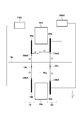
- An X blade and a Y blade are included between the first light-shielding portion 18 and the second light-shielding portion 20, specifically, in the vicinity of the conjugate surface 19a or the conjugate surface 19a which is a surface conjugated to the illuminated surface 24.
- a masking unit (masking unit) 19 is arranged and illuminated with a light intensity distribution having a substantially rectangular shape. The vicinity of the conjugate surface 19a is separated from the conjugate surface 19a by a distance required to prevent the X blade and the Y blade of the masking unit 19 from interfering with each other, for example, in the optical axis direction from the conjugate surface 19a. It means that the distance is about 0.2 mm.
- the masking unit 19 is arranged to define the illumination range of the original plate 25 (illuminated surface 24), and is scanned in synchronization with the original plate stage 29 and the substrate stage 28.
- the original plate stage 29 is a stage for holding and moving the original plate 25, and the substrate stage 28 is a stage for holding and moving the substrate 27.
- a first light-shielding portion 18 and a second light-shielding portion 20 are provided at positions separated (defocused) from the masking unit 19 (conjugate surface 19a of the illuminated surface 24). ..
- the first light-shielding portion 18 is arranged at a position away from the conjugate surface 19a of the illuminated surface 24 on the light source side.
- the second light-shielding portion 20 is arranged at a position away from the conjugate surface 19a of the illuminated surface 24 on the illuminated surface side.
- the light reflected by the mirror 22 having a predetermined inclination with respect to the light flux from the condenser lens 21 illuminates the original plate 25 via the collimator lens 23.
- the projection optical system 26 projects the pattern of the original plate 25 onto the substrate 27.
- the resolution of the pattern of the original plate 25 depends on the shape of the effective light source. Therefore, by forming an appropriate effective light source distribution in the illumination optical system 110, the resolvability of the pattern of the original plate 25 can be improved.
- the details of the first light-shielding unit 18, the masking unit 19, and the second light-shielding unit 20 will be described with reference to FIG.
- the y direction indicates the scanning direction.
- the masking unit 19 includes scan masking blades 19d and 19e that move during scan exposure.
- the first light-shielding unit 18 includes a first light-shielding member 18a and a second light-shielding member 18b.
- the end 18aA of the first light-shielding member 18a on the side of the second light-shielding member and the end 18bA of the second light-shielding member 18b on the side of the first light-shielding member are located in the light effective region and block a part of the light.
- the intensity of the light reaching the illuminated surface 24 is adjusted.
- an actuator (not shown) is connected to the first light-shielding member 18a.
- the first light-shielding member 18a By moving the first light-shielding member 18a along the scanning direction (y direction) by such an actuator, the opening width defined by the end portion 18aA of the first light-shielding member 18a and the end portion 18bA of the second light-shielding member 18b can be obtained. Can be changed. In this way, the first light-shielding portion 18 constitutes a variable slit. Further, in the present embodiment, the first light-shielding unit 18 is provided with a first moving unit FMU that moves the first light-shielding member 18a and the second light-shielding member 18b in the direction along the optical axis 1b of the illumination optical system 110. Has been done.
- FMU first moving unit
- the second light-shielding unit 20 includes a third light-shielding member 20a and a fourth light-shielding member 20b.
- the end portion 20aA of the third light-shielding member 20a on the side of the fourth light-shielding member and the end portion 20bA of the fourth light-shielding member 20b on the side of the third light-shielding member are located in the light effective region and shield a part of the light beam.
- An actuator (not shown) is connected to the third light-shielding member 20a.
- the opening width defined by the end portion 20aA of the third light-shielding member 20a and the end portion 20bA of the fourth light-shielding member 20b can be obtained. Can be changed. In this way, the second light-shielding portion 20 constitutes a variable slit. Further, in the present embodiment, the second light-shielding unit 20 is provided with a second moving unit SMU that moves the third light-shielding member 20a and the fourth light-shielding member 20b in the direction along the optical axis 1b of the illumination optical system 110. Has been done.
- a first distance between the conjugate surface 19a in the direction along the optical axis 1b and the end portion 18aA of the first shading member 18a Let d1. Further, in a plane including the optical axis 1b and parallel to the scanning direction, the second distance between the conjugate surface 19a and the end portion 20aA of the third light-shielding member 20a in the direction along the optical axis 1b is d2. In this case, the first distance d1 and the second distance d2 are different values.
- the distance between the conjugate surface 19a and the end 18bA of the second light-shielding member 18b is equal to the first distance d1
- the distance between the conjugate surface 19a and the end 20bA of the fourth light-shielding member 20b is the second distance. Equal to d2.
- the first light-shielding portion 18 and the second light-shielding portion 20 are arranged so that the first distance d1 and the second distance d2 are different.
- the midpoint between the end portion 18aA of the first light-shielding member 18a and the end portion 18bA of the second light-shielding member 18b is defined as 18c in a plane including the optical axis 1b and parallel to the scanning direction. To do.
- the midpoint between the end 20aA of the third light-shielding member 20a and the end 20bA of the fourth light-shielding member 20b is 20c.
- the distance from the midpoint 18c to the end 18aA of the first light-shielding member 18a and the end 18bA of the second light-shielding member 18b is S1
- the distance from the midpoint 20c to the end 20aA of the third light-shielding member 20a and the fourth light-shielding member 20b Let S2 be the distance to the end 20bA. In this case, the distance S1 and the distance S2 are different values.
- the straight line connecting the midpoint 18c and the midpoint 20c is parallel to the optical axis 1b.
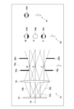
- FIGS. 3a and 3b The integrated effective light source will be described with reference to FIGS. 3a and 3b.
- the y direction indicates the scanning direction.
- FIG. 3a shows the illuminated area 24e of the illuminated surface 24
- FIG. 3b shows the illuminated area 19b of the conjugate surface 19a (masking unit 19) which has a conjugate relationship with the illuminated surface 24.
- the illumination area 24e is scanned.
- the incident angle distribution that illuminates a certain point on the exposed surface is the sum of the incident angle distributions that illuminate each point of the straight line 24f parallel to the scanning direction (y direction) in the illumination region 24e. It is called an integrated effective light source. Since the straight line 19c is a set of points conjugated to each point of the straight line 24e on the conjugate surface 19a, the integrated effective light source integrates the incident angle distribution that illuminates the illuminated surface 24 with the light beam passing through each point of the straight line 19c. Equivalent to one.
- FIGS. 4a, 4b, and 4c the y direction indicates the scanning direction.
- FIG. 4a is an enlarged view of the vicinity of the optical integrator 12, the condenser lens 14, the first light-shielding portion 18, and the second light-shielding portion 20.
- FIG. 4a shows a light beam that emits the optical integrator 12 and passes through the points A, B, and C of the conjugate surface 19a through the condenser lens 14.
- points A, B, and C are points on the straight line 19 shown in FIG. 3b.
- FIG. 4b is a diagram showing effective light sources 24a, 24b and 24c at points A', B'and C'of the illuminated surface 24, respectively.
- Each of the points A', B'and C' has a conjugate relationship with the points A, B and C of the conjugate surface 19a of the illuminated surface 24.
- FIG. 4c is a diagram showing an integrated effective light source 24d in which all light rays passing on a straight line including points A', B'and C'of the illuminated surface 24 are integrated.
- the effective light source has a circular shape called conventional illumination
- a ring band will be described. And multiple poles.
- the present invention is not limited by the shape of the effective light source formed by the diffractive optical element 6 and the prism unit 10.
- the light rays 12a emitted from the optical integrator 12 in parallel with the optical axis 1b and directed to the point A of the conjugated surface 19a via the condenser lens 14 are the first light-shielding portion 18 and the second light-shielding portion 20. Not shaded by. Therefore, the effective light source 24a at the point A'on the illuminated surface 24 is substantially circular and substantially symmetrical in the scanning direction, as shown in FIG. 4b.
- the effective light source 24b at the point B'of the illuminated surface 24 has a shape in which both ends in the scanning direction are missing from the circular shape, and is between the distribution in the x direction (the direction orthogonal to the y direction) and the distribution in the y direction. Has asymmetry (XY asymmetry).
- the effective light source 24c at the point C'of the illuminated surface 24 has a shape in which both ends in the scanning direction are missing from the circular shape, and is between the distribution in the x direction (the direction orthogonal to the y direction) and the distribution in the y direction. Has asymmetry (XY asymmetry).
- the integrated effective light source 24d has XY asymmetry as shown in FIG. 4c. ..
- FIG. 5a is a diagram showing an illumination distribution 24ee (illumination region 24e) that illuminates the illuminated surface 24 formed by a luminous flux that illuminates the conjugated surface 19a at a maximum angle ⁇ 0.
- the condenser lens 21 and the collimator lens 23 With the condenser lens 21 and the collimator lens 23, the distribution of the conjugated surface 19a is imaged on the illuminated surface 24 at an imaging magnification ⁇ .
- ⁇ 0 be the maximum incident angle of the luminous flux that illuminates the conjugated surface 19a.
- the first light ray having an angle ⁇ 0 passing through the end portion 18aA of the first light-shielding member 18a and the light ray having an angle ⁇ 0 passing through the end portion 20aA of the third light-shielding member 20a intersect at a point 19aa on the conjugated surface 19a.
- the distance S1 and the second distance S2 are determined. As described above, the first distance S1 is the distance from the midpoint 18c to the end 18aA of the first light-shielding member 18a, and the second distance S2 is the distance from the midpoint 20c to the end of the third light-shielding member 20a. The distance to 20aA.
- the illumination distribution 24ee has a shape close to a trapezoid. Let w0 and w100 be the lower base and the upper base of the trapezoid, respectively.
- the effective light source that illuminates the point between the point 24i and the point 24g of the illuminated surface 24 is substantially circular like the effective light source at the point A'described above.
- the effective light source that illuminates the point between the points 24g and 24h of the illuminated surface 24 has a large XY asymmetry, similar to the effective light source at the point B'described above.
- both the first light-shielding portion 18 and the second light-shielding portion 20 block light, so that the illuminance decreases. Therefore, by increasing the ratio of w100 to w0 and reducing the distance between the points 24g and 24h, it is possible to suppress the decrease in illuminance and the occurrence of XY asymmetry of the integrated effective light source 24d.
- the scan masking blades 19d and 19e are arranged between the first light-shielding portion 18 and the second light-shielding portion 20.
- the scan masking blades 19d and 19e require some space because they move during scan exposure. Therefore, the distance between the first light-shielding portion 18 and the second light-shielding portion 20 in the direction along the optical axis 1b cannot be made smaller than the predetermined value D.
- the predetermined value D is 5 mm or more and 20 mm or less.
- the vertical axis represents w100 / w0 and the horizontal axis represents d1 / d2.
- the illuminance is reduced by correcting the XY asymmetry. If it is necessary to reduce the XY asymmetry to 15% or less in order to reduce such a decrease in illuminance, it is preferable to set w100 / w0 to 0.7 or more. With reference to FIG. 6, it can be seen that d2 / d1> 2 or d2 / d1 ⁇ 1/2 is required in order to set w100 / w0 to 0.7 or more.
- the points C'and B'shown in FIG. 4b corresponding to the inclined portion of the illumination distribution 24ee have a shift of the center of gravity of the light beam (shift of the center of gravity light beam) in the scanning direction.
- the ray center of gravity shift is not preferable because it affects the superposition accuracy, but the ray center of gravity shift can be controlled by the ratio of d1 and d2.
- FIG. 7 assumes conventional illumination, and in the present embodiment, the light ray center of gravity shift of a conventional configuration, specifically, a configuration in which a light-shielding portion is arranged only on the upstream side of the conjugate surface of the illuminated surface, is set to 1. It shows the shift of the center of gravity of the ray.
- the vertical axis represents the shift of the center of gravity of the light beam
- the horizontal axis represents d1 / d2.
- the ray center of gravity shift is the minimum value at d2 / d1, specifically 0. This means that the ray center of gravity shift does not occur.
- the shift of the center of gravity of the light beam is less than half of the conventional configuration in which the light-shielding portion is arranged only on the upstream side of the conjugate surface of the illuminated surface.
- 1/4 ⁇ d2 / d1 ⁇ 4 is required in order to reduce the shift of the center of gravity of the light beam to less than half of the conventional configuration.
- the condition that the first distance d1 from the conjugate surface 19a to the first light-shielding portion 18 and the second distance d2 from the conjugate surface 19a to the second light-shielding portion 20 should be satisfied is d1 ⁇ d2, and more preferably 1 / 4 ⁇ d2 / d1 ⁇ 1/2 or 2 ⁇ d2 / d1 ⁇ 4.
- it is preferable that one of the first distance d1 and the second distance d2 is larger than twice the distance of the other and smaller than four times.
- the actuator for moving the first light-shielding member 18a along the scanning direction and the first light-shielding portion 18 are attached to the optical axis 1b.
- a first moving portion FMU that moves in the direction along the line is provided.
- the actuator that moves the third light-shielding member 20a along the scanning direction and the second light-shielding portion 20 are moved in the direction along the optical axis 1b.
- a section SMU is provided.
- the method for manufacturing an article according to the embodiment of the present invention is suitable for producing an article such as a flat panel display, a liquid crystal display element, a semiconductor element, or a MEMS.
- Such a manufacturing method includes a step of exposing a substrate coated with a photosensitizer using the above-mentioned exposure apparatus 100 and a step of developing the exposed photosensitizer. Further, the substrate is subjected to an etching step, an ion implantation step, or the like using the developed photosensitizer pattern as a mask to form a circuit pattern on the substrate. By repeating these steps such as exposure, development, and etching, a circuit pattern composed of a plurality of layers is formed on the substrate.
- dicing processing
- chip mounting, bonding, and inspection processes are performed.
- a manufacturing method may include other well-known steps (oxidation, film formation, vapor deposition, doping, flattening, resist stripping, etc.).
- the method for producing a good in the present embodiment is advantageous in at least one of the performance, quality, productivity and production cost of the good as compared with the conventional method.
Landscapes
- Physics & Mathematics (AREA)
- General Physics & Mathematics (AREA)
- Exposure And Positioning Against Photoresist Photosensitive Materials (AREA)
- Exposure Of Semiconductors, Excluding Electron Or Ion Beam Exposure (AREA)
- Developing Agents For Electrophotography (AREA)
- Apparatuses And Processes For Manufacturing Resistors (AREA)
Priority Applications (3)
| Application Number | Priority Date | Filing Date | Title |
|---|---|---|---|
| CN202080060934.8A CN114303101B (zh) | 2019-09-03 | 2020-07-21 | 曝光装置以及物品的制造方法 |
| KR1020227010183A KR102654989B1 (ko) | 2019-09-03 | 2020-07-21 | 노광장치 및 물품의 제조방법 |
| CN202310823157.3A CN116774533A (zh) | 2019-09-03 | 2020-07-21 | 曝光装置以及物品的制造方法 |
Applications Claiming Priority (2)
| Application Number | Priority Date | Filing Date | Title |
|---|---|---|---|
| JP2019-160666 | 2019-09-03 | ||
| JP2019160666A JP7336922B2 (ja) | 2019-09-03 | 2019-09-03 | 露光装置及び物品の製造方法 |
Publications (1)
| Publication Number | Publication Date |
|---|---|
| WO2021044756A1 true WO2021044756A1 (ja) | 2021-03-11 |
Family
ID=74849210
Family Applications (1)
| Application Number | Title | Priority Date | Filing Date |
|---|---|---|---|
| PCT/JP2020/028196 Ceased WO2021044756A1 (ja) | 2019-09-03 | 2020-07-21 | 露光装置及び物品の製造方法 |
Country Status (5)
| Country | Link |
|---|---|
| JP (1) | JP7336922B2 (https=) |
| KR (1) | KR102654989B1 (https=) |
| CN (2) | CN116774533A (https=) |
| TW (2) | TWI797466B (https=) |
| WO (1) | WO2021044756A1 (https=) |
Citations (5)
| Publication number | Priority date | Publication date | Assignee | Title |
|---|---|---|---|---|
| JP2004319770A (ja) * | 2003-04-16 | 2004-11-11 | Nikon Corp | 露光方法及びデバイス製造方法 |
| JP2010073835A (ja) * | 2008-09-17 | 2010-04-02 | Canon Inc | 露光装置及びデバイス製造方法 |
| WO2011010560A1 (ja) * | 2009-07-24 | 2011-01-27 | 株式会社ニコン | 照明光学系、露光装置、およびデバイス製造方法 |
| JP2011155040A (ja) * | 2010-01-26 | 2011-08-11 | Nikon Corp | 露光方法及び露光装置、並びにデバイス製造方法 |
| JP2017215487A (ja) * | 2016-06-01 | 2017-12-07 | キヤノン株式会社 | 走査露光装置および物品製造方法 |
Family Cites Families (13)
| Publication number | Priority date | Publication date | Assignee | Title |
|---|---|---|---|---|
| EP0633506B1 (en) * | 1993-06-11 | 2004-10-20 | Nikon Corporation | Scanning exposure apparatus |
| JPH08211787A (ja) * | 1995-02-08 | 1996-08-20 | Ricoh Co Ltd | 画像形成装置 |
| JP2000010013A (ja) * | 1998-06-24 | 2000-01-14 | Nikon Corp | 位相差顕微鏡及び重ね合わせ測定装置 |
| JP4392879B2 (ja) | 1998-09-28 | 2010-01-06 | キヤノン株式会社 | 投影露光装置及びデバイスの製造方法 |
| JP3571945B2 (ja) * | 1998-12-07 | 2004-09-29 | キヤノン株式会社 | 照明装置及びそれを用いた投影露光装置 |
| JP2000223406A (ja) | 1999-02-03 | 2000-08-11 | Nikon Corp | 露光装置および露光方法 |
| FR2831765B1 (fr) * | 2001-10-31 | 2004-02-13 | Automa Tech Sa | Dispositif pour insoler une face d'un panneau |
| JP3718511B2 (ja) * | 2003-10-07 | 2005-11-24 | 株式会社東芝 | 露光装置検査用マスク、露光装置検査方法及び露光装置 |
| JP2009302354A (ja) | 2008-06-16 | 2009-12-24 | Canon Inc | 露光装置、デバイス製造方法及び開口絞りの製造方法 |
| JP5396885B2 (ja) | 2009-01-29 | 2014-01-22 | 株式会社ニコン | 遮光ユニット、照明光学系、露光装置及びデバイスの製造方法 |
| JP2011040716A (ja) | 2009-08-06 | 2011-02-24 | Nikon Corp | 露光装置、露光方法、およびデバイス製造方法 |
| JP2011228556A (ja) * | 2010-04-22 | 2011-11-10 | Nikon Corp | 可変スリット装置、照明光学系、露光装置、およびデバイス製造方法 |
| JP2015079807A (ja) * | 2013-10-16 | 2015-04-23 | キヤノン株式会社 | 投影露光装置及び露光条件計算装置 |
-
2019
- 2019-09-03 JP JP2019160666A patent/JP7336922B2/ja active Active
-
2020
- 2020-07-21 CN CN202310823157.3A patent/CN116774533A/zh active Pending
- 2020-07-21 CN CN202080060934.8A patent/CN114303101B/zh active Active
- 2020-07-21 KR KR1020227010183A patent/KR102654989B1/ko active Active
- 2020-07-21 WO PCT/JP2020/028196 patent/WO2021044756A1/ja not_active Ceased
- 2020-08-03 TW TW109126156A patent/TWI797466B/zh active
- 2020-08-03 TW TW112108465A patent/TWI847583B/zh active
Patent Citations (5)
| Publication number | Priority date | Publication date | Assignee | Title |
|---|---|---|---|---|
| JP2004319770A (ja) * | 2003-04-16 | 2004-11-11 | Nikon Corp | 露光方法及びデバイス製造方法 |
| JP2010073835A (ja) * | 2008-09-17 | 2010-04-02 | Canon Inc | 露光装置及びデバイス製造方法 |
| WO2011010560A1 (ja) * | 2009-07-24 | 2011-01-27 | 株式会社ニコン | 照明光学系、露光装置、およびデバイス製造方法 |
| JP2011155040A (ja) * | 2010-01-26 | 2011-08-11 | Nikon Corp | 露光方法及び露光装置、並びにデバイス製造方法 |
| JP2017215487A (ja) * | 2016-06-01 | 2017-12-07 | キヤノン株式会社 | 走査露光装置および物品製造方法 |
Also Published As
| Publication number | Publication date |
|---|---|
| JP2021039245A (ja) | 2021-03-11 |
| TWI847583B (zh) | 2024-07-01 |
| TWI797466B (zh) | 2023-04-01 |
| TW202111450A (zh) | 2021-03-16 |
| KR20220050999A (ko) | 2022-04-25 |
| JP7336922B2 (ja) | 2023-09-01 |
| TW202328830A (zh) | 2023-07-16 |
| CN116774533A (zh) | 2023-09-19 |
| CN114303101B (zh) | 2023-07-07 |
| CN114303101A (zh) | 2022-04-08 |
| KR102654989B1 (ko) | 2024-04-05 |
Similar Documents
| Publication | Publication Date | Title |
|---|---|---|
| KR20080056094A (ko) | 노광 장치 및 디바이스 제조 방법 | |
| US8305560B2 (en) | Exposure apparatus, device manufacturing method, and aperture stop manufacturing method | |
| US11762298B2 (en) | Exposure apparatus and method of manufacturing article | |
| WO2021044756A1 (ja) | 露光装置及び物品の製造方法 | |
| KR102731783B1 (ko) | 노광 장치, 및 물품제조 방법 | |
| JP4950795B2 (ja) | 露光装置、デバイス製造方法及び補正方法 | |
| JP5396885B2 (ja) | 遮光ユニット、照明光学系、露光装置及びデバイスの製造方法 | |
| JP5239830B2 (ja) | 照明光学系、露光装置及びデバイスの製造方法 | |
| JP2008124308A (ja) | 露光方法及び露光装置、それを用いたデバイス製造方法 | |
| JP5532620B2 (ja) | 照明光学系、露光装置及びデバイスの製造方法 | |
| JP2023148840A (ja) | 照明光学系、露光装置および物品製造方法 | |
| JP2021067734A (ja) | 露光装置、露光方法及び物品の製造方法 | |
| JP2008277347A (ja) | 露光装置及びデバイス製造方法 |
Legal Events
| Date | Code | Title | Description |
|---|---|---|---|
| 121 | Ep: the epo has been informed by wipo that ep was designated in this application |
Ref document number: 20861153 Country of ref document: EP Kind code of ref document: A1 |
|
| NENP | Non-entry into the national phase |
Ref country code: DE |
|
| ENP | Entry into the national phase |
Ref document number: 20227010183 Country of ref document: KR Kind code of ref document: A |
|
| 122 | Ep: pct application non-entry in european phase |
Ref document number: 20861153 Country of ref document: EP Kind code of ref document: A1 |