WO2021039761A1 - フィルムコンデンサ - Google Patents
フィルムコンデンサ Download PDFInfo
- Publication number
- WO2021039761A1 WO2021039761A1 PCT/JP2020/031955 JP2020031955W WO2021039761A1 WO 2021039761 A1 WO2021039761 A1 WO 2021039761A1 JP 2020031955 W JP2020031955 W JP 2020031955W WO 2021039761 A1 WO2021039761 A1 WO 2021039761A1
- Authority
- WO
- WIPO (PCT)
- Prior art keywords
- external
- external electrode
- film
- release material
- extraction terminal
- Prior art date
- Legal status (The legal status is an assumption and is not a legal conclusion. Google has not performed a legal analysis and makes no representation as to the accuracy of the status listed.)
- Ceased
Links
Images






Classifications
-
- H—ELECTRICITY
- H01—ELECTRIC ELEMENTS
- H01G—CAPACITORS; CAPACITORS, RECTIFIERS, DETECTORS, SWITCHING DEVICES, LIGHT-SENSITIVE OR TEMPERATURE-SENSITIVE DEVICES OF THE ELECTROLYTIC TYPE
- H01G4/00—Fixed capacitors; Processes of their manufacture
- H01G4/002—Details
- H01G4/224—Housing; Encapsulation
-
- H—ELECTRICITY
- H01—ELECTRIC ELEMENTS
- H01G—CAPACITORS; CAPACITORS, RECTIFIERS, DETECTORS, SWITCHING DEVICES, LIGHT-SENSITIVE OR TEMPERATURE-SENSITIVE DEVICES OF THE ELECTROLYTIC TYPE
- H01G4/00—Fixed capacitors; Processes of their manufacture
- H01G4/002—Details
- H01G4/228—Terminals
-
- H—ELECTRICITY
- H01—ELECTRIC ELEMENTS
- H01G—CAPACITORS; CAPACITORS, RECTIFIERS, DETECTORS, SWITCHING DEVICES, LIGHT-SENSITIVE OR TEMPERATURE-SENSITIVE DEVICES OF THE ELECTROLYTIC TYPE
- H01G4/00—Fixed capacitors; Processes of their manufacture
- H01G4/002—Details
- H01G4/228—Terminals
- H01G4/232—Terminals electrically connecting two or more layers of a stacked or rolled capacitor
-
- H—ELECTRICITY
- H01—ELECTRIC ELEMENTS
- H01G—CAPACITORS; CAPACITORS, RECTIFIERS, DETECTORS, SWITCHING DEVICES, LIGHT-SENSITIVE OR TEMPERATURE-SENSITIVE DEVICES OF THE ELECTROLYTIC TYPE
- H01G4/00—Fixed capacitors; Processes of their manufacture
- H01G4/32—Wound capacitors
-
- H—ELECTRICITY
- H01—ELECTRIC ELEMENTS
- H01G—CAPACITORS; CAPACITORS, RECTIFIERS, DETECTORS, SWITCHING DEVICES, LIGHT-SENSITIVE OR TEMPERATURE-SENSITIVE DEVICES OF THE ELECTROLYTIC TYPE
- H01G4/00—Fixed capacitors; Processes of their manufacture
- H01G4/33—Thin- or thick-film capacitors (thin- or thick-film circuits; capacitors without a potential-jump or surface barrier specially adapted for integrated circuits, details thereof, multistep manufacturing processes therefor)
Definitions
- the present invention relates to a film capacitor.
- the film capacitor has a capacitor element in which a metallized film having a metal layer provided on the surface of a dielectric film is wound or laminated.
- a capacitor element is manufactured, for example, by laminating or laminating two metallized films and then forming a pair of external electrodes on both end faces thereof. Then, after forming the external lead-out terminal connected to the external electrode, the capacitor element may be housed in the outer case, and the filling resin may be filled in the outer case.
- the linear expansion coefficient of the metallized film laminate (including the wound body) is larger than the linear expansion coefficient of the filling resin, so that the external electrode becomes the surrounding filling resin.
- the laminate of the metallized film tries to shrink. Therefore, tensile stress is generated in the external electrode, and cracks occur.
- the film capacitor has a problem that cracks occur in the external electrode when used in a wide temperature range.
- high reliability is required in a wide temperature range, and therefore, it is important to solve the above problems.
- Patent Document 1 describes a case in which the upper end surface is open and a single or a plurality of capacitor elements housed in the case in which metallized films are used and metallikon electrodes are provided at both ends.
- a metallized film capacitor comprising an external lead-out terminal connected to a metallikon electrode and a resin composition for burying a capacitor element filled in a case, and the metallikon electrode coated with a release material.
- the metallikon electrode is coated with a release material, but there is room for improvement in suppressing the infiltration of water into the external electrode.
- the present invention has been made to solve the above problems, and an object of the present invention is to provide a film capacitor in which the occurrence of cracks in an external electrode is suppressed and the infiltration of water into the external electrode is suppressed. Is what you do.
- the film capacitor of the present invention is a laminate in which a film containing a metallized film having a metal layer provided on a main surface of a dielectric film is laminated in the lamination direction, and the laminate in a width direction orthogonal to the lamination direction.
- An outer case having an opening at one end and accommodating the capacitor element inside, and a filling resin filled in the outer case and burying the capacitor element are provided, and the laminate is the outer case.
- the release material has an upper surface located on the opening side of the above, covers the connection portion of the external extraction terminal with the external electrode and the external electrode, and covers at least a part of the upper surface of the laminate.
- the filler is not covered and is provided in a region surrounded by the external electrode, the external extraction terminal, and the release material, and in a region between the release material and the outer case.
- the present invention it is possible to provide a film capacitor in which the occurrence of cracks in the external electrode is suppressed and the infiltration of water into the external electrode is suppressed.
- FIG. 1 It is a perspective schematic diagram which shows an example of the film capacitor of this invention. It is a perspective schematic diagram which shows the state which disassembled the film capacitor in FIG. It is sectional drawing which shows the part corresponding to the line segment A1-A2 in FIG. It is sectional drawing which shows the part corresponding to the line segment B1-B2 in FIG. It is sectional drawing which shows the part corresponding to the line segment C1-C2 in FIG. It is a perspective schematic diagram which shows the capacitor element in FIG. It is sectional drawing which shows the part corresponding to the line segment D1-D2 in FIG. It is a perspective schematic diagram which shows the 1st method about the process of providing the release material in the manufacturing method of the film capacitor of this invention.
- the film capacitor of the present invention will be described.
- the present invention is not limited to the following configuration, and may be appropriately modified without departing from the gist of the present invention.
- a combination of a plurality of individual preferred configurations described below is also the present invention.
- Film capacitor As an example of the film capacitor of the present invention, a so-called winding type film in which a film containing a metallized film having a metal layer provided on at least one main surface of a dielectric film is wound in a laminated state.
- the capacitor will be described below.
- the film capacitor of the present invention may be a so-called laminated film capacitor in which the above films are laminated.
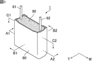
- FIG. 1 is a schematic perspective view showing an example of the film capacitor of the present invention.
- FIG. 2 is a schematic perspective view showing a state in which the film capacitor in FIG. 1 is disassembled.
- FIG. 2 shows a state before the capacitor element with the external extraction terminal is housed in the outer case.
- FIG. 3 is a schematic cross-sectional view showing a portion corresponding to the line segments A1-A2 in FIG.
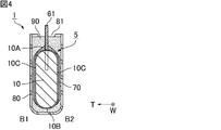
- FIG. 4 is a schematic cross-sectional view showing a portion corresponding to the line segments B1-B2 in FIG.
- FIG. 5 is a schematic cross-sectional view showing a portion corresponding to the line segments C1-C2 in FIG.
- the stacking direction and the width direction of the film capacitor are defined by arrows T and W, respectively, as shown in FIGS. 1, 2, 3, 4, and 5, respectively. It can be said that the winding type film capacitor has a plurality of stacking directions, but in the present specification, the direction is defined by the arrow T.
- the stacking direction T and the width direction W are orthogonal to each other.
- the film capacitor 1 is peeled off from the capacitor element 5, the first external extraction terminal 61, and the second external extraction terminal 62. It has a material 70, an outer case 80, and a filling resin 90.
- FIG. 6 is a schematic perspective view showing the capacitor element in FIG.
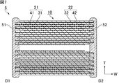
- FIG. 7 is a schematic cross-sectional view showing a portion corresponding to the line segments D1-D2 in FIG.
- the capacitor element 5 includes a laminate 10, a first external electrode 51 provided on one end surface of the laminate 10 in the width direction W, and a laminate in the width direction W. It has a second external electrode 52 provided on the other end face of the ten.
- both end faces of the laminated body 10 face each other in the width direction W.
- the laminated body 10 has an upper surface 10A, a lower surface 10B, and a side surface 10C in addition to both end faces provided with the first external electrode 51 and the second external electrode 52.
- the upper surface 10A of the laminated body 10 is located on the opening 81 side of the outer case 80.
- the lower surface 10B of the laminated body 10 faces the upper surface 10A and is located on the bottom surface side of the outer case 80.
- the side surfaces 10C of the laminated body 10 are a pair of surfaces facing each other in the stacking direction T. As shown in FIG. 4, the upper surface 10A and the lower surface 10B of the laminated body 10 may be rounded.
- the laminated body 10 is a wound body in which the first metallized film 21 and the second metallized film 22 are wound in a state of being laminated in the stacking direction T.
- the film capacitor 1 is a winding type film capacitor having a laminated body 10 which is also such a winding body.
- the cross-sectional shape of the laminated body 10 is pressed into a flat shape such as an ellipse or an oval, and the cross-sectional shape of the laminated body 10 is a perfect circle. It is preferable that the shape has a small thickness.
- the capacitor element 5 may have a columnar winding shaft.
- the winding shaft is arranged on the central axis of the first metallized film 21 and the second metallized film 22 in the wound state, and the first metallized film 21 and the second metallized film 22 are arranged. It serves as a winding shaft when winding 22.
- the first metallized film 21 has a first metal layer 41 provided on one main surface of the first dielectric film 31.
- the first metal layer 41 is provided so as to reach one side edge of the first metallized film 21 and not reach the other side edge of the first metallized film 21 in the width direction W.
- the second metallized film 22 is one in which a second metal layer 42 is provided on one main surface of the second dielectric film 32.
- the second metal layer 42 is provided so as not to reach one side edge of the second metallized film 22 but to reach the other side edge of the second metallized film 22 in the width direction W.
- the end portion of the first metal layer 41 on the side reaching the side edge of the first metallized film 21 is exposed on one end surface of the laminated body 10, and the second metal layer 42
- the adjacent first metallized film 21 and the second metallized film 22 are arranged so that the end portion on the side reaching the side edge of the second metallized film 22 is exposed to the other end surface of the laminated body 10. It is deviated in the width direction W.
- the laminate 10 is wound in a state where the first metallized film 21 and the second metallized film 22 are laminated in the lamination direction T, the first metal layer 41 and the first dielectric material are formed. It can also be said that the film 31, the second metal layer 42, and the second dielectric film 32 are wound in a state of being laminated in order in the stacking direction T.
- the first metallized film 21 is inside the second metallized film 22, the first metal layer 41 is inside the first dielectric film 31, and the second metal layer 42 is inside.
- the first metallized film 21 and the second metallized film 22 are wound in a laminated state in the stacking direction T so as to be inside the second dielectric film 32.
- the second metal layer 42 may be provided not on one main surface of the second dielectric film 32 but on the other main surface of the first dielectric film 31.
- the first metal layer 41 is provided on one main surface of the first dielectric film 31, and the second metal layer 42 is provided on the other main surface.
- the metallized film and the second dielectric film 32 are wound in a state of being laminated in the stacking direction T.
- the first dielectric film 31 and the second dielectric film 32 each contain a curable resin as a main component.
- the principal component means a component having the largest weight percentage, and preferably means a component having a weight percentage larger than 50% by weight.
- the curable resin may be a thermosetting resin or a photocurable resin.
- the thermosetting resin means a resin that can be cured by heat, and does not limit the curing method. Therefore, as long as the resin can be cured by heat, the thermosetting resin also includes a resin cured by a method other than heat (for example, light, electron beam, etc.). Further, depending on the material, the reaction may be started due to the reactivity of the material itself, and a thermosetting resin is also used if the material is cured without necessarily applying heat or light from the outside. The same applies to the photocurable resin, and the curing method is not limited as long as the resin can be cured by light.
- the curable resin may have at least one of urethane bond and urea bond, and may not have both urethane bond and urea bond.
- the presence of urethane bond and / or urea bond can be confirmed by using a Fourier transform infrared spectrophotometer (FT-IR).
- FT-IR Fourier transform infrared spectrophotometer
- the curable resin is preferably composed of a cured product of the first organic material and the second organic material.
- a cured product include a cured product obtained by reacting a hydroxyl group (OH group) contained in the first organic material with an isocyanate group (NCO group) contained in the second organic material.
- NCO group isocyanate group
- the first dielectric film 31 and the second dielectric film 32 may each contain one of a hydroxyl group and an isocyanate group, or may contain both a hydroxyl group and an isocyanate group. ..
- the presence of hydroxyl groups and / or isocyanate groups can be confirmed using a Fourier transform infrared spectrophotometer.
- the first organic material is preferably a polyol having a plurality of hydroxyl groups in the molecule.
- the polyol include polyvinyl acetal such as polyvinyl acetal acetal, polyether polyol such as phenoxy resin, polyester polyol and the like.
- the first organic material a plurality of types of organic materials may be used in combination.
- the second organic material is preferably an isocyanate compound, an epoxy resin, or a melamine resin having a plurality of functional groups in the molecule.
- a plurality of types of organic materials may be used in combination.
- isocyanate compound examples include aromatic polyisocyanates such as diphenylmethane diisocyanate (MDI) and tolylene diisocyanate (TDI), and aliphatic polyisocyanates such as hexamethylene diisocyanate (HDI).
- aromatic polyisocyanates such as diphenylmethane diisocyanate (MDI) and tolylene diisocyanate (TDI)
- aliphatic polyisocyanates such as hexamethylene diisocyanate (HDI).
- the isocyanate compound may be a modified product of these polyisocyanates, for example, a modified product having carbodiimide, urethane, or the like.
- the epoxy resin is not particularly limited as long as it has an epoxy ring, and examples thereof include a bisphenol A type epoxy resin, a biphenyl skeleton epoxy resin, a cyclopentadiene skeleton epoxy resin, and a naphthalene skeleton epoxy resin.
- the melamine resin is not particularly limited as long as it is an organic nitrogen compound having a triazine ring at the center of the structure and three amino groups around it, and examples thereof include alkylated melamine resins.
- the melamine resin may be a modified form of melamine.
- the first dielectric film 31 and the second dielectric film 32 are preferably formed by forming a resin solution containing the first organic material and the second organic material into a film, and then heat-treating and curing the resin solution. It is made.
- the first dielectric film 31 and the second dielectric film 32 may each contain a vapor-deposited polymer film as a main component.
- the vapor-deposited polymerized film may have at least one of a urethane bond and a urea bond, or may not have both a urethane bond and a urea bond.
- the thin-film deposition polymer film refers to a film formed by a thin-film deposition polymerization method, and is basically included in a curable resin.
- the first dielectric film 31 and the second dielectric film 32 may each contain a thermoplastic resin as a main component.
- thermoplastic resin examples include polypropylene, polyether sulfone, polyetherimide, polyarylate and the like.
- Each of the first dielectric film 31 and the second dielectric film 32 has uncured portions of starting materials such as silicone resin, first organic material and second organic material as components other than the main components. Etc. may be contained.
- the first dielectric film 31 and the second dielectric film 32 may each contain additives for adding various functions.
- the additive include a leveling agent for imparting smoothness.
- the additive preferably has a functional group that reacts with a hydroxyl group and / or an isocyanate group, and forms a part of the crosslinked structure of the cured product.
- examples of such an additive include a resin having at least one functional group selected from the group consisting of a hydroxyl group, an epoxy group, a silanol group, and a carboxyl group.
- compositions of the first dielectric film 31 and the second dielectric film 32 may be different from each other, but are preferably the same.
- the thickness of the first dielectric film 31 and the second dielectric film 32 is preferably 0.5 ⁇ m or more and 5 ⁇ m or less, respectively.
- the thicknesses of the first dielectric film 31 and the second dielectric film 32 may be different from each other, but are preferably the same.
- the thickness of the first dielectric film 31 and the second dielectric film 32 can be measured using an optical film thickness meter.
- Examples of the constituent materials of the first metal layer 41 and the second metal layer 42 include metals such as aluminum, zinc, titanium, magnesium, tin, and nickel, respectively.
- compositions of the first metal layer 41 and the second metal layer 42 may be different from each other, but are preferably the same.
- the thicknesses of the first metal layer 41 and the second metal layer 42 are preferably 5 nm or more and 40 nm or less, respectively.
- the thickness of the first metal layer 41 can be specified by observing the cut surface of the first metallized film 21 in the thickness direction using a transmission electron microscope (TEM).
- the thickness of the second metal layer 42 can be specified in the same manner.
- the first external electrode 51 is provided on one end surface of the laminated body 10 and is connected to the first metal layer 41 by coming into contact with the exposed end portion of the first metal layer 41.
- the first metallized film 21 has a width with respect to the second metallized film 22. It is preferable that it protrudes in the direction W.
- the second external electrode 52 is provided on the other end surface of the laminated body 10 and is connected to the second metal layer 42 by coming into contact with the exposed end portion of the second metal layer 42.
- the second metallized film 22 has a width with respect to the first metallized film 21. It is preferable that it protrudes in the direction W.
- first external electrode 51 and the second external electrode 52 examples include metals such as zinc, aluminum, tin, and zinc-aluminum alloy.
- the first external electrode 51 and the second external electrode 52 are preferably formed by spraying a metal as described above onto one end face and the other end face of the laminate 10, respectively.
- compositions of the first external electrode 51 and the second external electrode 52 may be different from each other, but are preferably the same.
- the configuration of the laminated body 10 may be different from the configuration as shown in FIG.
- the first metal layer 41 is divided into two metal layers in the width direction W, one metal layer reaches one side edge of the first metallized film 21, and the other.
- the metal layer may be provided so as to reach the other side edge of the first metallized film 21.
- one metal layer is connected to the first external electrode 51, and the other metal layer is connected to the second external electrode 52, while the second metal layer 42 is connected. Is provided so as not to be connected to both the first external electrode 51 and the second external electrode 52, a capacitor can be formed between the first metal layer 41 and the second metal layer 42.
- the first external extraction terminal 61 is connected to the first external electrode 51.
- the first external lead-out terminal 61 may be electrically connected to the first external electrode 51 via, for example, a solder layer.
- the first external drawer terminal 61 projects from the inside of the outer case 80 toward the outside.
- connection position between the first external lead-out terminal 61 and the first external electrode 51 may be the central portion of the first external electrode 51, as described in FIG. 1 of Japanese Patent No. 4733566. It may be the end of the first external electrode 51 close to the opening 81 of the outer case 80.
- the second external extraction terminal 62 is connected to the second external electrode 52.
- the second external extraction terminal 62 may be electrically connected to the second external electrode 52, for example, via a solder layer.
- the second external drawer terminal 62 projects from the inside of the outer case 80 toward the outside.
- connection position between the second external extraction terminal 62 and the second external electrode 52 may be the central portion of the second external electrode 52, as described in FIG. 1 of Japanese Patent No. 4733566. It may be the end of the second external electrode 52 close to the opening 81 of the outer case 80.
- Examples of the constituent materials of the first external lead-out terminal 61 and the second external lead-out terminal 62 include metals such as copper, tin, and aluminum.
- compositions of the first external extraction terminal 61 and the second external extraction terminal 62 may be different from each other, but are preferably the same.
- the shape of the first external drawer terminal 61 and the second external drawer terminal 62 may be linear (rod-shaped) or plate-shaped.
- the shapes of the first external extraction terminal 61 and the second external extraction terminal 62 may be different from each other, but are preferably the same.
- the outer case 80 is provided with an opening 81 at one end and houses the capacitor element 5 inside.
- the shape of the outer case 80 is not particularly limited as long as it has an opening 81 at one end, and is, for example, a bottomed square cylinder having a square cylindrical side wall portion as shown in FIG. It may be a bottomed cylinder having a cylindrical side wall portion.
- Examples of the constituent material of the outer case 80 include metals such as aluminum, magnesium, iron, stainless steel, and copper, alloys of these metals, resins such as polybutylene terephthalate, polyphenylene sulfide, and liquid crystal polymer (LCP). ..
- the constituent material of the outer case 80 is a metal or alloy as described above, the water vapor barrier property of the outer case 80 is enhanced. Therefore, even if the film capacitor 1 is used in a high temperature and high humidity environment, the hydroxylation reaction of the first metal layer 41 and the second metal layer 42 due to the infiltration of water is less likely to proceed, and as a result, it becomes difficult to proceed. The decrease in capacitance is suppressed. On the other hand, since the conductivity of the outer case 80 is also increased, it may be necessary to take measures for insulation between the first external drawer terminal 61 and the second external drawer terminal 62 and the outer case 80.
- the outer case 80 is manufactured by, for example, impact molding or the like.
- the constituent material of the exterior case 80 is a resin composition containing a resin having high insulating properties as described above, the above-mentioned insulating measures are not required.
- the resin composition constituting the outer case 80 contains a liquid crystal polymer, the water vapor barrier property of the outer case 80 is enhanced.
- liquid crystal polymer contained in the resin composition examples include a liquid crystal polymer having a p-hydroxybenzoic acid and a 6-hydroxy-2-naphthoic acid group in the skeleton.
- a liquid crystal polymer having a polycondensate formed by using various components such as phenol, phthalic acid, and ethylene terephthalate can be used.
- classification methods such as type I, type II, and type III, but the material means the same material as the liquid crystal polymer formed from the above components.
- the content of the liquid crystal polymer in the resin composition is preferably 40% by weight or more and 95% by weight or less, and more preferably 40% by weight or more and 85% by weight or less.
- the resin composition preferably contains an inorganic filler in addition to the liquid crystal polymer.
- an inorganic filler a material having higher strength than the liquid crystal polymer can be used.
- the inorganic filler is preferably a material having a melting point higher than that of the liquid crystal polymer, and more preferably a material having a melting point of 680 ° C. or higher.
- the form of the inorganic filler is not particularly limited, and examples thereof include a form having a longitudinal direction such as a fibrous shape or a plate shape. A plurality of types of inorganic materials may be used in combination as the inorganic filler having such a form.
- the resin composition preferably contains at least one of a fibrous inorganic material and a plate-shaped inorganic material as the inorganic filler.
- the fibrous means that the relationship between the longitudinal length of the filler in the longitudinal direction and the cross-sectional diameter in the cross section perpendicular to the longitudinal direction is the longitudinal length / cross-sectional diameter ⁇ 5 (that is, the aspect ratio is It means a state of 5: 1 or more).
- the cross-sectional diameter is the longest distance between two points on the outer circumference of the cross-section. If the cross-sectional diameter differs in the longitudinal direction, the measurement is performed at the point where the cross-sectional diameter is maximum.
- the plate shape means a state in which the relationship between the cross-sectional diameter of the surface having the maximum projected area and the maximum height in the direction perpendicular to this cross-section is cross-sectional diameter / maximum height ⁇ 3. To do.
- the resin composition may contain an inorganic filler that satisfies both the fibrous and plate-like conditions described above.
- the inorganic filler contains only one type of inorganic material.
- the resin composition contains both a fibrous inorganic material and a plate-shaped inorganic material as an inorganic filler.
- the inorganic filler has a portion that is oriented toward the opening 81 from the bottom side and a portion that is oriented toward the adjacent side wall in each side wall of the side portion of the exterior case 80. It is preferable that it has and is dispersed inside the outer case 80.
- the size of the inorganic filler is preferably a size having a diameter of 5 ⁇ m or more and a length of 50 ⁇ m or more.
- the inorganic filler is dispersed throughout the outer case 80 without agglomeration.
- inorganic filler examples include inorganic materials such as glass fiber, mica, talc, various oxides, and various hydroxides.
- the content of the inorganic filler in the resin composition is preferably 5% by weight or more, more preferably 15% by weight or more. Further, from the viewpoint of ensuring the moldability of the outer case 80, the content of the inorganic filler in the resin composition is preferably 60% by weight or less.
- the content of the inorganic filler in the resin composition is measured by measuring the residual component as an inorganic component by ash content measurement or thermogravimetric analysis using a test piece having a thickness of 20 mm ⁇ 20 mm ⁇ 0.5 mm. It can be calculated from the measured initial weight and residual component weight. More specifically, based on the JIS K 7250 A method (direct ashing method), the organic material is burned and the combustion residue is measured by heating it at a high temperature until it becomes constant.
- the outer case 80 is manufactured by, for example, injection molding or the like.
- the release material 70 includes a part of the capacitor element 5, a part of the first external extraction terminal 61, and a part of the second external extraction terminal 62. It covers and. More specifically, the release material 70 covers a part of the surface of the first external electrode 51 and the second external electrode 52 located on the opening 81 side of the outer case 80. Further, the release material 70 covers the connection portion of the first external extraction terminal 61 with the first external electrode 51 and the connection portion of the second external extraction terminal 62 with the second external electrode 52. ..
- the first external extraction terminal 61 and the second external extraction terminal 62 are electrically connected to the first external electrode 51 and the second external electrode 52, respectively, via a solder layer.
- the connection portion of the first external extraction terminal 61 with the first external electrode 51 and the connection portion of the second external extraction terminal 62 with the second external electrode 52 each include a solder layer.
- the release material 70 is a connection portion between the first external electrode 51 and the first external electrode 51 in the first external extraction terminal 61, a second external electrode 52, and a second external extraction terminal 62.
- the connection portion of 2 with the external electrode 52 By covering the connection portion of 2 with the external electrode 52, the connection portion between the first external electrode 51 and the first external electrode 51 at the first external extraction terminal 61, and the second external electrode 52 , The connection portion of the second external extraction terminal 62 with the second external electrode 52 is less likely to be bound by the filling resin 90 described later. Therefore, even if the film capacitor 1 is moved to a low temperature environment or a high temperature environment, tensile stress is less likely to occur in the first external electrode 51 and the second external electrode 52. As a result, the occurrence of cracks in the first external electrode 51 and the second external electrode 52 is suppressed.
- the release material 70 does not cover at least a part of the upper surface 10A of the laminated body 10. More specifically, the release material 70 does not cover a part of the upper surface 10A of the laminated body 10, or does not cover the entire upper surface 10A of the laminated body 10.
- the release material 70 has a first external extraction terminal 61 and a second external extraction terminal 61 when the capacitor element 5 with the first external extraction terminal 62 and the second external extraction terminal 62 is viewed from the upper surface 10A side of the laminated body 10. It does not have to cover the area connecting the drawer terminal 62.
- the width of such a region is preferably equal to or greater than the width of the smaller of the widths of the first external extraction terminal 61 and the second external extraction terminal 62.
- the release material 70 does not cover at least a part of the upper surface 10A of the laminate 10, a part of the upper surface 10A comes into contact with the filling resin 90 described later. Therefore, the infiltration of water from the opening 81 of the outer case 80 into the upper surface 10A of the laminated body 10 is suppressed.
- release material 70 does not cover a part of the upper surface 10A of the laminate 10, that is, covers a part of the upper surface 10A of the laminate 10, a part of the upper surface 10A of the laminate 10 covered with the release material 70. May be in close contact with the release material 70.
- the release material 70 does not have to cover at least a part of the lower surface 10B of the laminated body 10. More specifically, the release material 70 may not cover a part of the lower surface 10B of the laminated body 10, or may not cover the entire lower surface 10B of the laminated body 10. Since the release material 70 does not cover at least a part of the lower surface 10B of the laminate 10, a part of the lower surface 10B comes into contact with the filling resin 90 described later. Therefore, the infiltration of water from the opening 81 of the outer case 80 into the lower surface 10B of the laminated body 10 is suppressed.
- the release material 70 may cover the side surface 10C of the laminate 10.
- the release material 70 can be easily fixed. Further, since the side surface 10C of the laminated body 10 is less likely to be restrained by the filling resin 90 described later, the stress generated in the laminated body 10 when the film capacitor 1 is moved to a low temperature environment or a high temperature environment is relaxed.
- release material 70 examples include a biaxially stretched polypropylene film, a polyester adhesive tape (Mylar tape), and the like.
- connection portion between the first external electrode 51 and the first external electrode 51 in the first external extraction terminal 61, the second external electrode 52, and the second external For example, a biaxially stretched polypropylene film is drawn from the first external drawing so as to cover the connection portion of the drawing terminal 62 with the second external electrode 52 and not to cover at least a part of the upper surface 10A of the laminated body 10.
- Examples thereof include a method of providing the capacitor element 5 with the terminal 61 and the second external extraction terminal 62 so as to be wound around the capacitor element 5. A specific example of the method of providing the release material 70 in this way will be described later.
- FIGS. 1, 2, 3, 4, and 5 a state in which a single capacitor element 5 is housed in a single exterior case 80 is illustrated, but is described in, for example, Patent Document 1.
- a plurality of capacitor elements 5 may be housed in a single exterior case 80.
- the release material 70 may be individually provided on the plurality of capacitor elements 5, or may be provided alone so as to bundle the plurality of capacitor elements 5.
- the thickness of the release material 70 is preferably 12 ⁇ m or more and 50 ⁇ m or less.
- the thickness of the release material 70 can be measured using an optical film thickness meter.
- the release material 70 is in at least in contact with the corner portion where the pair of side surfaces of the first external electrode 51 in the stacking direction T and the end surface in the width direction W intersect with the first external extraction terminal 61. However, it is at least not in contact with the end face of the first external electrode 51. Therefore, there is a region surrounded by the first external electrode 51, the first external extraction terminal 61, and the release material 70. Similarly, the release material 70 is in contact with at least the corner portion where the pair of side surfaces of the second external electrode 52 in the stacking direction T and the end surface in the width direction W intersect with the second external extraction terminal 62, and the second external electrode 52 is in contact with the second external electrode 52. At least not in contact with the end face of the external electrode 52.
- the filling resin 90 is filled from the opening 81 of the outer case 80, at least a part of the upper surface 10A of the laminate 10 not covered with the release material 70 is connected to the first external electrode 51. It enters the region surrounded by the first external extraction terminal 61 and the release material 70, and the region surrounded by the second external electrode 52, the second external extraction terminal 62, and the release material 70. Therefore, as shown in FIG. 5, in the film capacitor 1, the filled resin 90 is surrounded by the first external electrode 51, the first external extraction terminal 61, and the release material 70, and the second outer surface. It is provided in a region surrounded by the electrode 52, the second external extraction terminal 62, and the release material 70.
- the release material 70 does not have to cover at least a part of the lower surface 10B of the laminate 10, but in this case, the filling resin 90 is the lower surface 10B of the laminate 10 not covered with the release material 70.
- the filling resin 90 is provided in the area surrounded by the first external electrode 51, the first external extraction terminal 61, and the release material 70, so that the first external electrode 51 comes into contact with the filling resin 90. Therefore, the infiltration of water from the opening 81 of the outer case 80 into the first external electrode 51 is suppressed.
- the filling resin 90 is provided in the area surrounded by the second external electrode 52, the second external extraction terminal 62, and the release material 70, so that the second external electrode 52 comes into contact with the filling resin 90. Therefore, the infiltration of water from the opening 81 of the outer case 80 into the second external electrode 52 is suppressed.
- connection portion of the first external extraction terminal 61 with the first external electrode 51 and the connection portion of the second external extraction terminal 62 with the second external electrode 52 are small, in a conventional film capacitor, When a load is applied to the first external extraction terminal 61 and the second external extraction terminal 62, the first external extraction terminal 61 is separated from the first external electrode 51, and the second external extraction terminal 62 is the second. There is a risk of separation from the external electrode 52 of 2.
- the region surrounded by the first external electrode 51, the first external extraction terminal 61 and the release material 70, and the second external electrode 52 and the second external extraction terminal Since the filling resin 90 is provided in the region surrounded by the release material 70, the connection portion between the first external electrode 51 and the first external extraction terminal 61 is reinforced, and the second external electrode 52 and the second external electrode 52 are reinforced.
- the connection portion with the second external extraction terminal 62 is reinforced.
- the filling resin 90 is filled through the opening 81 of the outer case 80, it also enters the region between the release material 70 and the outer case 80. Therefore, as shown in FIG. 5, in the film capacitor 1, the filling resin 90 is provided in the region between the release material 70 and the outer case 80.
- the filling resin 90 may be provided in the region between the side surface 10C of the laminate 10 and the release material 70.
- the filling resin 90 may be provided in the region between the side surface 10C of the laminated body 10 and the release material 70.
- the side surface 10C of the laminated body 10 comes into contact with the filling resin 90. Therefore, the infiltration of water from the opening 81 of the outer case 80 into the side surface 10C of the laminated body 10 is suppressed.
- the filling resin 90 it is preferable to appropriately select a resin having low moisture permeability from the viewpoint of suppressing the infiltration of water into the capacitor element 5, and examples thereof include epoxy resin, silicone resin, and urethane resin.
- examples of the epoxy resin curing agent include amine curing agents and imidazole curing agents.
- a reinforcing agent may be added to the filling resin 90 for the purpose of improving the strength.
- the reinforcing agent include silica, alumina and the like.
- the thickness of the filling resin 90 in the opening 81 of the outer case 80 is large.
- the thickness of the filling resin 90 in the opening 81 of the outer case 80 is preferably sufficiently large within an allowable range of the volume (physique) of the entire film capacitor 1, specifically, preferably 2 mm or more, more preferably 4 mm. That is all.
- the thickness of the filling resin 90 with respect to the capacitor element 5 can be adjusted to the bottom surface on the opening 81 side of the exterior case 80. It is preferable to make it larger than the side.
- the thickness of the filling resin 90 can be measured using a soft X-ray device if it is in a non-destructive state, and can be measured using a length measuring device such as a caliper if it is in a broken state.
- the relationship between the height of the filling resin 90 and the height of the outer case 80 is such that the thickness of the filling resin 90 at the opening 81 of the outer case 80 may be made as large as possible, and may be up to the position on the inner side of the outer case 80. It may be full, or it may be slightly overflowed due to surface tension.
- the film capacitor of the present invention is manufactured by, for example, the following method.
- a resin solution is prepared by mixing the above-mentioned first organic material, second organic material, additives and the like. Then, the obtained resin solution is formed into a film and then heat-treated and cured to produce a first dielectric film and a second dielectric film.
- the first metal layer is formed.
- a metal such as aluminum, zinc, titanium, magnesium, tin, or nickel
- a second metal layer is formed by depositing a metal such as aluminum, zinc, titanium, magnesium, tin, or nickel on one main surface of the second dielectric film to form a second metal layer. Make a metallized film. At this time, the second metal layer is formed so as not to reach one side edge of the second metallized film in the width direction but to reach the other side edge of the second metallized film.
- a metal such as aluminum, zinc, titanium, magnesium, tin, or nickel
- the second metal layer may be formed not on one main surface of the second dielectric film but on the other main surface of the first dielectric film.
- the first metal layer is formed so as to reach one side edge of the metallized film and not reach the other side edge of the metallized film, and one side edge of the metallized film is formed.
- the second metal layer may be formed so as to reach the other side edge of the metallized film without reaching.
- the first metallized film and the second metallized film are stacked in a state of being shifted by a predetermined distance in the width direction, and then wound to produce a laminated body (winding body). If necessary, the obtained laminate may be sandwiched from a direction perpendicular to the width direction and pressed into an elliptical cylinder shape.
- the first external electrode is connected to the first metal layer by spraying a metal such as zinc, aluminum, tin, or zinc-aluminum alloy onto one end face of the laminate.
- the second external electrode is formed so as to be connected to the second metal layer by spraying a metal such as zinc, aluminum, tin, or zinc-aluminum alloy onto the other end face of the laminate. To do.
- the capacitor element is manufactured.
- the first external lead-out terminal is provided so as to be connected to the first external electrode, for example, via a solder layer. Further, the second external extraction terminal is provided so as to be connected to the second external electrode via, for example, a solder layer.
- the constituent materials of the first external lead-out terminal and the second external lead-out terminal are, for example, metals such as copper, tin, and aluminum, respectively.
- a biaxially stretched polypropylene film is provided so as to be wrapped around a capacitor element having a first external extraction terminal and a second external extraction terminal so as to cover and not cover at least a part of the upper surface of the laminate.
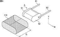
- FIGS. 8 and 9 are schematic perspective views showing a first method for providing a release material in the method for manufacturing a film capacitor of the present invention.
- a shrink film 170 such as a biaxially stretched polypropylene film is formed into a tubular shape by heat-sealing the ends with a heat seal.
- the shrink film 170 will later become the release material 70.
- the width G of the shrink film 170 is the direction of the capacitor element 5 in the direction orthogonal to the stacking direction T and the width direction W (in FIG. 8, the direction in which the first external extraction terminal 61 and the second external extraction terminal 62 extend). It is preferably larger than the length.
- the capacitor element 5 with the first external extraction terminal 61 and the second external extraction terminal 62 provided with the release material 70 is formed. obtain. More specifically, in the connection portion between the first external electrode 51 and the first external electrode 51 in the first external extraction terminal 61, the second external electrode 52, and the second external extraction terminal 62.
- the release material 70 is provided so as to cover the connection portion with the second external electrode 52 and not to cover at least a part of the upper surface 10A of the laminated body 10.
- the release material 70 has traces of the heat seal of the shrink film 170 as described above.
- the trace of such a heat seal exists in the release material 70 at a position facing the side surface 10C of the laminated body 10, for example.
- the shape of the heat seal may be point-shaped or planar.
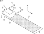
- FIGS. 10 and 11 are schematic perspective views showing a second method for a step of providing a release material in the method for manufacturing a film capacitor of the present invention.
- a shrink film 170 such as a biaxially stretched polypropylene film is fixed to the side surface 10C of the laminated body 10 of the capacitor element 5 by heat fusion by heat sealing.
- the shape of the heat seal may be point-shaped or planar.
- the width G of the shrink film 170 is the direction of the capacitor element 5 in the direction orthogonal to the stacking direction T and the width direction W (in FIG. 10, the direction in which the first external extraction terminal 61 and the second external extraction terminal 62 extend). It is preferably larger than the length.
- the shrink film 170 is wound around the capacitor element 5 with the first external extraction terminal 61 and the second external extraction terminal 62 so as to cover the capacitor element 5.
- the shrink film 170 may be wound for one round or for two or more turns.
- the other end of the shrink film 170 is fixed to a part of the shrink film 170, for example, a position facing the side surface 10C of the laminate 10 in the shrink film 170 by heat fusion by heat sealing. ..
- the shape of the heat seal may be point-shaped or planar.
- the capacitor element 5 with the first external extraction terminal 61 and the second external extraction terminal 62 provided with the release material 70 is formed. obtain. More specifically, in the connection portion between the first external electrode 51 and the first external electrode 51 in the first external extraction terminal 61, the second external electrode 52, and the second external extraction terminal 62.
- the release material 70 is provided so as to cover the connection portion with the second external electrode 52 and not to cover at least a part of the upper surface 10A of the laminated body 10.
- an exterior case having an opening at one end is produced by injection molding using a resin composition containing a highly insulating resin such as polybutylene terephthalate, polyphenylene sulfide, and a liquid crystal polymer.
- a resin composition containing a highly insulating resin such as polybutylene terephthalate, polyphenylene sulfide, and a liquid crystal polymer.
- an outer case having an opening at one end may be produced by impact molding using a metal such as aluminum, magnesium, iron, stainless steel, or copper, or an alloy thereof.
- the capacitor element with the first external extraction terminal and the second external extraction terminal provided with the release material is housed inside the outer case.
- a filling resin such as an epoxy resin, a silicone resin, or a urethane resin is filled through the opening of the outer case, and the capacitor element is buried.
- the filling resin is formed from at least a part of the upper surface of the laminate not covered with the release material, a region surrounded by the first external electrode, the first external extraction terminal, and the release material, and the second. It enters the area surrounded by the external electrode, the second external extraction terminal, and the release material.
- the filling resin also enters the area between the release material and the outer case.
- the filling resin contains a region surrounded by the first external electrode, the first external extraction terminal, and the release material, a region surrounded by the second external electrode, the second external extraction terminal, and the release material, and It will be provided in the area between the release material and the outer case.
- the film capacitor of the present invention is manufactured.
- Example 1 The film capacitor of Example 1 was manufactured by the following method.
- a resin solution was prepared by mixing phenoxy resin, which is a bisphenol A type epoxy resin as a first organic material, and diphenylmethane diisocyanate, which is a second organic material, at a weight ratio of 7: 3. Then, the obtained resin solution was formed into a film and then heat-treated and cured to prepare a first dielectric film and a second dielectric film. The thickness of the first dielectric film and the second dielectric film was 3 ⁇ m.
- the first metal layer was formed so as to reach one side edge of the first metallized film and not reach the other side edge of the first metallized film.
- the thickness of the first metal layer was 20 nm.
- a second metallized film was produced by depositing aluminum on one main surface of the second dielectric film to form a second metal layer. At this time, the second metal layer was formed so as not to reach one side edge of the second metallized film in the width direction but to reach the other side edge of the second metallized film.
- the thickness of the second metal layer was 20 nm.
- the first metallized film and the second metallized film were laminated in a state of being shifted by a predetermined distance in the width direction, and then wound to prepare a laminated body (winding body). Then, the obtained laminate was sandwiched from a direction perpendicular to the width direction and pressed into an elliptical cylinder shape.
- the second external electrode was formed so as to be connected to the second metal layer by spraying zinc on the other end face of the laminated body.
- the capacitor element was manufactured.
- the first external lead-out terminal is provided so as to be connected to the first external electrode via a solder layer. Further, the second external lead-out terminal is provided so as to be connected to the second external electrode via the solder layer.
- the first external lead-out terminal and the second external lead-out terminal were each made of copper and had a tin-plated surface.
- connection portion between the first external electrode and the first external electrode in the first external extraction terminal, the second external electrode, and the second in the second external extraction terminal A biaxially stretched polypropylene film as a release material is provided as a first external extraction terminal and a second external extraction terminal so as to cover the connection portion with the external electrode and not to cover at least a part of the upper surface of the laminate. It was provided in the attached capacitor element.
- the heat treatment for shrinking the shrink film was carried out at 120 ° C. for 3 seconds using a hot air gun or a dryer.
- the thickness of the release material was 50 ⁇ m.
- the filling resin contains a region surrounded by the first external electrode, the first external extraction terminal, and the release material, a region surrounded by the second external electrode, the second external extraction terminal, and the release material, and It was provided in the area between the release material and the outer case.
- the film capacitor of Example 1 was manufactured for 5 samples.
- Comparative Example 1 A film capacitor of Comparative Example 1 was produced for 5 samples in the same manner as the film capacitor of Example 1 except that the step of providing the release material was not performed.
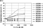
- Example 1 and Comparative Example 1 were subjected to a heat cycle test in a temperature range of ⁇ 40 ° C. or higher and 125 ° C. or lower.
- one cycle was defined as a cycle in which the film capacitor was transferred from a low temperature environment of ⁇ 40 ° C. to a high temperature environment of 125 ° C. and then from a high temperature environment of 125 ° C. to a low temperature environment of ⁇ 40 ° C.
- ESR equivalent series resistance
- Example 12 is a graph showing the measurement results of the rate of change of the equivalent series resistance with respect to the film capacitors of Example 1 and Comparative Example 1.
- Example 1-1 five samples of the film capacitor of Example 1 are used in "Example 1-1", “Example 1-2", “Example 1-3", “Example 1-4", and “Example 1-4". It is shown as “Example 1-5".
- 5 samples of the film capacitor of Comparative Example 1 were used as "Comparative Example 1-1", “Comparative Example 1-2”, “Comparative Example 1-3", “Comparative Example 1-4", and “Comparative Example 1". It is shown as -5 ".
- the equivalent series resistance before and after the heat cycle test at a predetermined number of cycles was measured using the LCR meter "ZM2371" manufactured by NF Circuit Design Block, and based on the following formula (F). Calculated.
- the measurement conditions for the equivalent series resistance were a measurement frequency of 10 kHz and a measurement voltage of 2 V. 100 x ["Equivalent series resistance after heat cycle test"-"Equivalent series resistance before heat cycle test”] / "Equivalent series resistance before heat cycle test” (F)
- the equivalent series resistance is stable even if the number of cycles is increased, and the occurrence of cracks in the first external electrode and the second external electrode is suppressed. It turned out that.
- the rate of change of the equivalent series resistance increased as the number of cycles increased, and the occurrence of cracks in the first external electrode and the second external electrode was not suppressed. It was.
Landscapes
- Engineering & Computer Science (AREA)
- Power Engineering (AREA)
- Microelectronics & Electronic Packaging (AREA)
- Manufacturing & Machinery (AREA)
- Fixed Capacitors And Capacitor Manufacturing Machines (AREA)
Priority Applications (2)
| Application Number | Priority Date | Filing Date | Title |
|---|---|---|---|
| JP2021542914A JP7244032B2 (ja) | 2019-08-30 | 2020-08-25 | フィルムコンデンサ |
| CN202080048739.3A CN114051646A (zh) | 2019-08-30 | 2020-08-25 | 薄膜电容器 |
Applications Claiming Priority (2)
| Application Number | Priority Date | Filing Date | Title |
|---|---|---|---|
| JP2019158672 | 2019-08-30 | ||
| JP2019-158672 | 2019-08-30 |
Publications (1)
| Publication Number | Publication Date |
|---|---|
| WO2021039761A1 true WO2021039761A1 (ja) | 2021-03-04 |
Family
ID=74685932
Family Applications (1)
| Application Number | Title | Priority Date | Filing Date |
|---|---|---|---|
| PCT/JP2020/031955 Ceased WO2021039761A1 (ja) | 2019-08-30 | 2020-08-25 | フィルムコンデンサ |
Country Status (3)
| Country | Link |
|---|---|
| JP (1) | JP7244032B2 (https=) |
| CN (1) | CN114051646A (https=) |
| WO (1) | WO2021039761A1 (https=) |
Citations (5)
| Publication number | Priority date | Publication date | Assignee | Title |
|---|---|---|---|---|
| JPH09232181A (ja) * | 1996-02-23 | 1997-09-05 | Nitsuko Corp | メタライズドフィルムコンデンサ |
| JPH09232182A (ja) * | 1996-02-26 | 1997-09-05 | Nitsuko Corp | メタライズドフィルムコンデンサ |
| JPH10214748A (ja) * | 1997-01-28 | 1998-08-11 | Nitsuko Corp | ケース入りフィルムコンデンサ |
| JP2003338424A (ja) * | 2002-05-22 | 2003-11-28 | Matsushita Electric Ind Co Ltd | コンデンサ |
| JP2007311625A (ja) * | 2006-05-19 | 2007-11-29 | Hitachi Aic Inc | 金属化フィルムコンデンサ |
Family Cites Families (5)
| Publication number | Priority date | Publication date | Assignee | Title |
|---|---|---|---|---|
| JPS55111324U (https=) * | 1979-01-30 | 1980-08-05 | ||
| JP2010016161A (ja) | 2008-07-03 | 2010-01-21 | Hitachi Chemical Electronics Co Ltd | 金属化フィルムコンデンサ |
| JP2010016160A (ja) * | 2008-07-03 | 2010-01-21 | Hitachi Chemical Electronics Co Ltd | 金属化フィルムコンデンサ |
| KR20130115263A (ko) * | 2010-09-24 | 2013-10-21 | 신코베덴키 가부시키가이샤 | 축전 디바이스 및 축전 디바이스의 제조 방법 |
| JP6890259B2 (ja) * | 2016-03-25 | 2021-06-18 | パナソニックIpマネジメント株式会社 | フィルムコンデンサ |
-
2020
- 2020-08-25 JP JP2021542914A patent/JP7244032B2/ja active Active
- 2020-08-25 WO PCT/JP2020/031955 patent/WO2021039761A1/ja not_active Ceased
- 2020-08-25 CN CN202080048739.3A patent/CN114051646A/zh active Pending
Patent Citations (5)
| Publication number | Priority date | Publication date | Assignee | Title |
|---|---|---|---|---|
| JPH09232181A (ja) * | 1996-02-23 | 1997-09-05 | Nitsuko Corp | メタライズドフィルムコンデンサ |
| JPH09232182A (ja) * | 1996-02-26 | 1997-09-05 | Nitsuko Corp | メタライズドフィルムコンデンサ |
| JPH10214748A (ja) * | 1997-01-28 | 1998-08-11 | Nitsuko Corp | ケース入りフィルムコンデンサ |
| JP2003338424A (ja) * | 2002-05-22 | 2003-11-28 | Matsushita Electric Ind Co Ltd | コンデンサ |
| JP2007311625A (ja) * | 2006-05-19 | 2007-11-29 | Hitachi Aic Inc | 金属化フィルムコンデンサ |
Also Published As
| Publication number | Publication date |
|---|---|
| JP7244032B2 (ja) | 2023-03-22 |
| CN114051646A (zh) | 2022-02-15 |
| JPWO2021039761A1 (https=) | 2021-03-04 |
Similar Documents
| Publication | Publication Date | Title |
|---|---|---|
| JP7057923B2 (ja) | フィルムコンデンサ、及び、フィルムコンデンサ用の外装ケース | |
| JP7300637B2 (ja) | ケースレスフィルムコンデンサの製造方法 | |
| JP7794316B2 (ja) | コンデンサ、コンデンサバンク、及び、コンデンサ用外装ケース | |
| CN103339699B (zh) | 薄膜电容器 | |
| JP7244032B2 (ja) | フィルムコンデンサ | |
| US20230250234A1 (en) | Resin composition, self-fusing insulated electric wire and wire bundle | |
| JP7829038B2 (ja) | フィルムコンデンサ | |
| JP7228855B2 (ja) | フィルムコンデンサ | |
| US11978593B2 (en) | Film capacitor and exterior case for film capacitor | |
| JP7428493B2 (ja) | フィルムコンデンサ | |
| US6465097B1 (en) | Insulated wire | |
| JP7839292B2 (ja) | コンデンサ | |
| WO2025109925A1 (ja) | コンデンサの実装構造体及び電力変換機器 | |
| WO2020166170A1 (ja) | フィルムコンデンサ、及び、フィルムコンデンサ用の外装ケース | |
| WO2024014111A1 (ja) | コンデンサ | |
| JP7568109B2 (ja) | フィルムコンデンサ | |
| WO2025032938A1 (ja) | フィルムコンデンサ | |
| WO2025047029A1 (ja) | コンデンサ | |
| JP2026068219A (ja) | コンデンサモジュール | |
| JP2026068221A (ja) | コンデンサモジュール | |
| WO2026058791A1 (ja) | コンデンサモジュール | |
| JP2026068220A (ja) | コンデンサモジュール | |
| JP2026068218A (ja) | コンデンサモジュール | |
| CN117321713A (zh) | 二次注塑薄膜电容器 | |
| WO2024070067A1 (ja) | フィルムコンデンサ及びモジュール |
Legal Events
| Date | Code | Title | Description |
|---|---|---|---|
| 121 | Ep: the epo has been informed by wipo that ep was designated in this application |
Ref document number: 20856127 Country of ref document: EP Kind code of ref document: A1 |
|
| ENP | Entry into the national phase |
Ref document number: 2021542914 Country of ref document: JP Kind code of ref document: A |
|
| NENP | Non-entry into the national phase |
Ref country code: DE |
|
| 122 | Ep: pct application non-entry in european phase |
Ref document number: 20856127 Country of ref document: EP Kind code of ref document: A1 |