WO2021039761A1 - Film capacitor - Google Patents
Film capacitor Download PDFInfo
- Publication number
- WO2021039761A1 WO2021039761A1 PCT/JP2020/031955 JP2020031955W WO2021039761A1 WO 2021039761 A1 WO2021039761 A1 WO 2021039761A1 JP 2020031955 W JP2020031955 W JP 2020031955W WO 2021039761 A1 WO2021039761 A1 WO 2021039761A1
- Authority
- WO
- WIPO (PCT)
- Prior art keywords
- external
- external electrode
- film
- release material
- extraction terminal
- Prior art date
Links
- 239000003990 capacitor Substances 0.000 title claims abstract description 129
- 239000010408 film Substances 0.000 claims abstract description 135
- 239000000463 material Substances 0.000 claims abstract description 118
- 229910052751 metal Inorganic materials 0.000 claims abstract description 83
- 239000002184 metal Substances 0.000 claims abstract description 83
- 229920005989 resin Polymers 0.000 claims abstract description 76
- 239000011347 resin Substances 0.000 claims abstract description 76
- 239000011104 metalized film Substances 0.000 claims abstract description 68
- 238000000605 extraction Methods 0.000 claims description 106
- 238000011049 filling Methods 0.000 claims description 48
- 238000010030 laminating Methods 0.000 claims description 4
- 239000000945 filler Substances 0.000 abstract description 4
- 238000000034 method Methods 0.000 description 39
- 239000011368 organic material Substances 0.000 description 19
- 229920006300 shrink film Polymers 0.000 description 18
- 239000011256 inorganic filler Substances 0.000 description 16
- 229910003475 inorganic filler Inorganic materials 0.000 description 16
- XLYOFNOQVPJJNP-UHFFFAOYSA-N water Substances O XLYOFNOQVPJJNP-UHFFFAOYSA-N 0.000 description 16
- 229920000106 Liquid crystal polymer Polymers 0.000 description 14
- 239000004977 Liquid-crystal polymers (LCPs) Substances 0.000 description 14
- 230000008595 infiltration Effects 0.000 description 14
- 238000001764 infiltration Methods 0.000 description 14
- 230000008569 process Effects 0.000 description 14
- 239000011342 resin composition Substances 0.000 description 14
- -1 acetal acetal Chemical class 0.000 description 13
- 229910052782 aluminium Inorganic materials 0.000 description 12
- XAGFODPZIPBFFR-UHFFFAOYSA-N aluminium Chemical compound [Al] XAGFODPZIPBFFR-UHFFFAOYSA-N 0.000 description 12
- 230000000052 comparative effect Effects 0.000 description 12
- 239000003822 epoxy resin Substances 0.000 description 11
- 229920000647 polyepoxide Polymers 0.000 description 11
- 238000004804 winding Methods 0.000 description 11
- 239000000470 constituent Substances 0.000 description 9
- 125000002887 hydroxy group Chemical group [H]O* 0.000 description 9
- 238000004519 manufacturing process Methods 0.000 description 9
- ATJFFYVFTNAWJD-UHFFFAOYSA-N Tin Chemical compound [Sn] ATJFFYVFTNAWJD-UHFFFAOYSA-N 0.000 description 8
- HCHKCACWOHOZIP-UHFFFAOYSA-N Zinc Chemical compound [Zn] HCHKCACWOHOZIP-UHFFFAOYSA-N 0.000 description 8
- 229910000679 solder Inorganic materials 0.000 description 8
- 229910052718 tin Inorganic materials 0.000 description 8
- 239000011135 tin Substances 0.000 description 8
- 229910052725 zinc Inorganic materials 0.000 description 8
- 239000011701 zinc Substances 0.000 description 8
- 239000004743 Polypropylene Substances 0.000 description 7
- 229910045601 alloy Inorganic materials 0.000 description 7
- 239000000956 alloy Substances 0.000 description 7
- 238000010586 diagram Methods 0.000 description 7
- 229910010272 inorganic material Inorganic materials 0.000 description 7
- 239000011147 inorganic material Substances 0.000 description 7
- 238000005259 measurement Methods 0.000 description 7
- 229920001155 polypropylene Polymers 0.000 description 7
- 238000012360 testing method Methods 0.000 description 7
- PXHVJJICTQNCMI-UHFFFAOYSA-N Nickel Chemical compound [Ni] PXHVJJICTQNCMI-UHFFFAOYSA-N 0.000 description 6
- 238000001723 curing Methods 0.000 description 6
- IQPQWNKOIGAROB-UHFFFAOYSA-N isocyanate group Chemical group [N-]=C=O IQPQWNKOIGAROB-UHFFFAOYSA-N 0.000 description 6
- 150000002739 metals Chemical class 0.000 description 6
- 239000000243 solution Substances 0.000 description 6
- RYGMFSIKBFXOCR-UHFFFAOYSA-N Copper Chemical compound [Cu] RYGMFSIKBFXOCR-UHFFFAOYSA-N 0.000 description 5
- FYYHWMGAXLPEAU-UHFFFAOYSA-N Magnesium Chemical compound [Mg] FYYHWMGAXLPEAU-UHFFFAOYSA-N 0.000 description 5
- 229920000877 Melamine resin Polymers 0.000 description 5
- 239000004202 carbamide Substances 0.000 description 5
- 230000008859 change Effects 0.000 description 5
- 229910052802 copper Inorganic materials 0.000 description 5
- 239000010949 copper Substances 0.000 description 5
- 229910052749 magnesium Inorganic materials 0.000 description 5
- 239000011777 magnesium Substances 0.000 description 5
- FJKROLUGYXJWQN-UHFFFAOYSA-N 4-hydroxybenzoic acid Chemical compound OC(=O)C1=CC=C(O)C=C1 FJKROLUGYXJWQN-UHFFFAOYSA-N 0.000 description 4
- XEEYBQQBJWHFJM-UHFFFAOYSA-N Iron Chemical compound [Fe] XEEYBQQBJWHFJM-UHFFFAOYSA-N 0.000 description 4
- 239000000654 additive Substances 0.000 description 4
- IISBACLAFKSPIT-UHFFFAOYSA-N bisphenol A Chemical compound C=1C=C(O)C=CC=1C(C)(C)C1=CC=C(O)C=C1 IISBACLAFKSPIT-UHFFFAOYSA-N 0.000 description 4
- 239000003795 chemical substances by application Substances 0.000 description 4
- 238000010438 heat treatment Methods 0.000 description 4
- 238000003475 lamination Methods 0.000 description 4
- 239000000203 mixture Substances 0.000 description 4
- 238000005507 spraying Methods 0.000 description 4
- 229920001187 thermosetting polymer Polymers 0.000 description 4
- UPMLOUAZCHDJJD-UHFFFAOYSA-N 4,4'-Diphenylmethane Diisocyanate Chemical compound C1=CC(N=C=O)=CC=C1CC1=CC=C(N=C=O)C=C1 UPMLOUAZCHDJJD-UHFFFAOYSA-N 0.000 description 3
- 238000005033 Fourier transform infrared spectroscopy Methods 0.000 description 3
- 239000004640 Melamine resin Substances 0.000 description 3
- MKYBYDHXWVHEJW-UHFFFAOYSA-N N-[1-oxo-1-(2,4,6,7-tetrahydrotriazolo[4,5-c]pyridin-5-yl)propan-2-yl]-2-[[3-(trifluoromethoxy)phenyl]methylamino]pyrimidine-5-carboxamide Chemical compound O=C(C(C)NC(=O)C=1C=NC(=NC=1)NCC1=CC(=CC=C1)OC(F)(F)F)N1CC2=C(CC1)NN=N2 MKYBYDHXWVHEJW-UHFFFAOYSA-N 0.000 description 3
- RTAQQCXQSZGOHL-UHFFFAOYSA-N Titanium Chemical compound [Ti] RTAQQCXQSZGOHL-UHFFFAOYSA-N 0.000 description 3
- 229910000611 Zinc aluminium Inorganic materials 0.000 description 3
- DHKHKXVYLBGOIT-UHFFFAOYSA-N acetaldehyde Diethyl Acetal Natural products CCOC(C)OCC DHKHKXVYLBGOIT-UHFFFAOYSA-N 0.000 description 3
- 230000000996 additive effect Effects 0.000 description 3
- HXFVOUUOTHJFPX-UHFFFAOYSA-N alumane;zinc Chemical compound [AlH3].[Zn] HXFVOUUOTHJFPX-UHFFFAOYSA-N 0.000 description 3
- 238000000151 deposition Methods 0.000 description 3
- 125000000524 functional group Chemical group 0.000 description 3
- RAXXELZNTBOGNW-UHFFFAOYSA-N imidazole Natural products C1=CNC=N1 RAXXELZNTBOGNW-UHFFFAOYSA-N 0.000 description 3
- 238000001746 injection moulding Methods 0.000 description 3
- 239000012948 isocyanate Substances 0.000 description 3
- 229910052759 nickel Inorganic materials 0.000 description 3
- 239000005056 polyisocyanate Substances 0.000 description 3
- 229920001228 polyisocyanate Polymers 0.000 description 3
- 229920005862 polyol Polymers 0.000 description 3
- 150000003077 polyols Chemical class 0.000 description 3
- 238000007789 sealing Methods 0.000 description 3
- 229920002050 silicone resin Polymers 0.000 description 3
- 239000010936 titanium Substances 0.000 description 3
- 229910052719 titanium Inorganic materials 0.000 description 3
- VZSRBBMJRBPUNF-UHFFFAOYSA-N 2-(2,3-dihydro-1H-inden-2-ylamino)-N-[3-oxo-3-(2,4,6,7-tetrahydrotriazolo[4,5-c]pyridin-5-yl)propyl]pyrimidine-5-carboxamide Chemical compound C1C(CC2=CC=CC=C12)NC1=NC=C(C=N1)C(=O)NCCC(N1CC2=C(CC1)NN=N2)=O VZSRBBMJRBPUNF-UHFFFAOYSA-N 0.000 description 2
- 229940090248 4-hydroxybenzoic acid Drugs 0.000 description 2
- KAUQJMHLAFIZDU-UHFFFAOYSA-N 6-Hydroxy-2-naphthoic acid Chemical group C1=C(O)C=CC2=CC(C(=O)O)=CC=C21 KAUQJMHLAFIZDU-UHFFFAOYSA-N 0.000 description 2
- 239000005057 Hexamethylene diisocyanate Substances 0.000 description 2
- NIPNSKYNPDTRPC-UHFFFAOYSA-N N-[2-oxo-2-(2,4,6,7-tetrahydrotriazolo[4,5-c]pyridin-5-yl)ethyl]-2-[[3-(trifluoromethoxy)phenyl]methylamino]pyrimidine-5-carboxamide Chemical compound O=C(CNC(=O)C=1C=NC(=NC=1)NCC1=CC(=CC=C1)OC(F)(F)F)N1CC2=C(CC1)NN=N2 NIPNSKYNPDTRPC-UHFFFAOYSA-N 0.000 description 2
- AFCARXCZXQIEQB-UHFFFAOYSA-N N-[3-oxo-3-(2,4,6,7-tetrahydrotriazolo[4,5-c]pyridin-5-yl)propyl]-2-[[3-(trifluoromethoxy)phenyl]methylamino]pyrimidine-5-carboxamide Chemical compound O=C(CCNC(=O)C=1C=NC(=NC=1)NCC1=CC(=CC=C1)OC(F)(F)F)N1CC2=C(CC1)NN=N2 AFCARXCZXQIEQB-UHFFFAOYSA-N 0.000 description 2
- 239000004734 Polyphenylene sulfide Substances 0.000 description 2
- VYPSYNLAJGMNEJ-UHFFFAOYSA-N Silicium dioxide Chemical compound O=[Si]=O VYPSYNLAJGMNEJ-UHFFFAOYSA-N 0.000 description 2
- 230000004888 barrier function Effects 0.000 description 2
- 238000006243 chemical reaction Methods 0.000 description 2
- ZUOUZKKEUPVFJK-UHFFFAOYSA-N diphenyl Chemical group C1=CC=CC=C1C1=CC=CC=C1 ZUOUZKKEUPVFJK-UHFFFAOYSA-N 0.000 description 2
- 230000004927 fusion Effects 0.000 description 2
- RRAMGCGOFNQTLD-UHFFFAOYSA-N hexamethylene diisocyanate Chemical compound O=C=NCCCCCCN=C=O RRAMGCGOFNQTLD-UHFFFAOYSA-N 0.000 description 2
- 229910052742 iron Inorganic materials 0.000 description 2
- 238000002844 melting Methods 0.000 description 2
- 230000008018 melting Effects 0.000 description 2
- 238000002156 mixing Methods 0.000 description 2
- 238000000465 moulding Methods 0.000 description 2
- 239000012788 optical film Substances 0.000 description 2
- 229920006287 phenoxy resin Polymers 0.000 description 2
- 239000013034 phenoxy resin Substances 0.000 description 2
- XNGIFLGASWRNHJ-UHFFFAOYSA-N phthalic acid Chemical compound OC(=O)C1=CC=CC=C1C(O)=O XNGIFLGASWRNHJ-UHFFFAOYSA-N 0.000 description 2
- 229920001707 polybutylene terephthalate Polymers 0.000 description 2
- 229920006254 polymer film Polymers 0.000 description 2
- 229920000069 polyphenylene sulfide Polymers 0.000 description 2
- 239000012744 reinforcing agent Substances 0.000 description 2
- 238000000926 separation method Methods 0.000 description 2
- 229910001220 stainless steel Inorganic materials 0.000 description 2
- 239000010935 stainless steel Substances 0.000 description 2
- 239000007858 starting material Substances 0.000 description 2
- 229920002803 thermoplastic polyurethane Polymers 0.000 description 2
- 229920005992 thermoplastic resin Polymers 0.000 description 2
- 238000000427 thin-film deposition Methods 0.000 description 2
- DVKJHBMWWAPEIU-UHFFFAOYSA-N toluene 2,4-diisocyanate Chemical compound CC1=CC=C(N=C=O)C=C1N=C=O DVKJHBMWWAPEIU-UHFFFAOYSA-N 0.000 description 2
- 229920002554 vinyl polymer Polymers 0.000 description 2
- JYEUMXHLPRZUAT-UHFFFAOYSA-N 1,2,3-triazine Chemical group C1=CN=NN=C1 JYEUMXHLPRZUAT-UHFFFAOYSA-N 0.000 description 1
- LLLVZDVNHNWSDS-UHFFFAOYSA-N 4-methylidene-3,5-dioxabicyclo[5.2.2]undeca-1(9),7,10-triene-2,6-dione Chemical compound C1(C2=CC=C(C(=O)OC(=C)O1)C=C2)=O LLLVZDVNHNWSDS-UHFFFAOYSA-N 0.000 description 1
- 229920002799 BoPET Polymers 0.000 description 1
- 239000004593 Epoxy Substances 0.000 description 1
- JOYRKODLDBILNP-UHFFFAOYSA-N Ethyl urethane Chemical compound CCOC(N)=O JOYRKODLDBILNP-UHFFFAOYSA-N 0.000 description 1
- ISWSIDIOOBJBQZ-UHFFFAOYSA-N Phenol Chemical compound OC1=CC=CC=C1 ISWSIDIOOBJBQZ-UHFFFAOYSA-N 0.000 description 1
- 239000004695 Polyether sulfone Substances 0.000 description 1
- 239000004697 Polyetherimide Substances 0.000 description 1
- 239000004721 Polyphenylene oxide Substances 0.000 description 1
- 125000002777 acetyl group Chemical class [H]C([H])([H])C(*)=O 0.000 description 1
- 239000002390 adhesive tape Substances 0.000 description 1
- 238000005054 agglomeration Methods 0.000 description 1
- 230000002776 aggregation Effects 0.000 description 1
- 125000001931 aliphatic group Chemical group 0.000 description 1
- PNEYBMLMFCGWSK-UHFFFAOYSA-N aluminium oxide Inorganic materials [O-2].[O-2].[O-2].[Al+3].[Al+3] PNEYBMLMFCGWSK-UHFFFAOYSA-N 0.000 description 1
- 150000001412 amines Chemical class 0.000 description 1
- 125000003277 amino group Chemical group 0.000 description 1
- 125000003118 aryl group Chemical group 0.000 description 1
- 238000004380 ashing Methods 0.000 description 1
- 230000005540 biological transmission Effects 0.000 description 1
- 235000010290 biphenyl Nutrition 0.000 description 1
- 239000004305 biphenyl Substances 0.000 description 1
- 150000001718 carbodiimides Chemical class 0.000 description 1
- 125000003178 carboxy group Chemical group [H]OC(*)=O 0.000 description 1
- 238000002485 combustion reaction Methods 0.000 description 1
- ZSWFCLXCOIISFI-UHFFFAOYSA-N cyclopentadiene Chemical group C1C=CC=C1 ZSWFCLXCOIISFI-UHFFFAOYSA-N 0.000 description 1
- 238000013461 design Methods 0.000 description 1
- 230000001066 destructive effect Effects 0.000 description 1
- 239000003989 dielectric material Substances 0.000 description 1
- 238000010894 electron beam technology Methods 0.000 description 1
- 125000003700 epoxy group Chemical group 0.000 description 1
- 238000011156 evaluation Methods 0.000 description 1
- 239000003365 glass fiber Substances 0.000 description 1
- 150000004679 hydroxides Chemical class 0.000 description 1
- 238000005805 hydroxylation reaction Methods 0.000 description 1
- 230000006872 improvement Effects 0.000 description 1
- 238000009413 insulation Methods 0.000 description 1
- JDSHMPZPIAZGSV-UHFFFAOYSA-N melamine Chemical compound NC1=NC(N)=NC(N)=N1 JDSHMPZPIAZGSV-UHFFFAOYSA-N 0.000 description 1
- 150000007974 melamines Chemical class 0.000 description 1
- 239000010445 mica Substances 0.000 description 1
- 229910052618 mica group Inorganic materials 0.000 description 1
- 125000001624 naphthyl group Chemical group 0.000 description 1
- 239000006259 organic additive Substances 0.000 description 1
- 150000002897 organic nitrogen compounds Chemical group 0.000 description 1
- 230000035699 permeability Effects 0.000 description 1
- 229920001230 polyarylate Polymers 0.000 description 1
- 229920000728 polyester Polymers 0.000 description 1
- 229920005906 polyester polyol Polymers 0.000 description 1
- 229920000570 polyether Polymers 0.000 description 1
- 229920006393 polyether sulfone Polymers 0.000 description 1
- 229920001601 polyetherimide Polymers 0.000 description 1
- 238000006116 polymerization reaction Methods 0.000 description 1
- 230000009257 reactivity Effects 0.000 description 1
- 230000004044 response Effects 0.000 description 1
- 125000005372 silanol group Chemical group 0.000 description 1
- 239000000377 silicon dioxide Substances 0.000 description 1
- 239000000454 talc Substances 0.000 description 1
- 229910052623 talc Inorganic materials 0.000 description 1
- 238000002411 thermogravimetry Methods 0.000 description 1
Images


Classifications
-
- H—ELECTRICITY
- H01—ELECTRIC ELEMENTS
- H01G—CAPACITORS; CAPACITORS, RECTIFIERS, DETECTORS, SWITCHING DEVICES, LIGHT-SENSITIVE OR TEMPERATURE-SENSITIVE DEVICES OF THE ELECTROLYTIC TYPE
- H01G4/00—Fixed capacitors; Processes of their manufacture
- H01G4/002—Details
- H01G4/224—Housing; Encapsulation
-
- H—ELECTRICITY
- H01—ELECTRIC ELEMENTS
- H01G—CAPACITORS; CAPACITORS, RECTIFIERS, DETECTORS, SWITCHING DEVICES, LIGHT-SENSITIVE OR TEMPERATURE-SENSITIVE DEVICES OF THE ELECTROLYTIC TYPE
- H01G4/00—Fixed capacitors; Processes of their manufacture
- H01G4/002—Details
- H01G4/228—Terminals
-
- H—ELECTRICITY
- H01—ELECTRIC ELEMENTS
- H01G—CAPACITORS; CAPACITORS, RECTIFIERS, DETECTORS, SWITCHING DEVICES, LIGHT-SENSITIVE OR TEMPERATURE-SENSITIVE DEVICES OF THE ELECTROLYTIC TYPE
- H01G4/00—Fixed capacitors; Processes of their manufacture
- H01G4/002—Details
- H01G4/228—Terminals
- H01G4/232—Terminals electrically connecting two or more layers of a stacked or rolled capacitor
-
- H—ELECTRICITY
- H01—ELECTRIC ELEMENTS
- H01G—CAPACITORS; CAPACITORS, RECTIFIERS, DETECTORS, SWITCHING DEVICES, LIGHT-SENSITIVE OR TEMPERATURE-SENSITIVE DEVICES OF THE ELECTROLYTIC TYPE
- H01G4/00—Fixed capacitors; Processes of their manufacture
- H01G4/32—Wound capacitors
-
- H—ELECTRICITY
- H01—ELECTRIC ELEMENTS
- H01G—CAPACITORS; CAPACITORS, RECTIFIERS, DETECTORS, SWITCHING DEVICES, LIGHT-SENSITIVE OR TEMPERATURE-SENSITIVE DEVICES OF THE ELECTROLYTIC TYPE
- H01G4/00—Fixed capacitors; Processes of their manufacture
- H01G4/33—Thin- or thick-film capacitors
Definitions
- the present invention relates to a film capacitor.
- the film capacitor has a capacitor element in which a metallized film having a metal layer provided on the surface of a dielectric film is wound or laminated.
- a capacitor element is manufactured, for example, by laminating or laminating two metallized films and then forming a pair of external electrodes on both end faces thereof. Then, after forming the external lead-out terminal connected to the external electrode, the capacitor element may be housed in the outer case, and the filling resin may be filled in the outer case.
- the linear expansion coefficient of the metallized film laminate (including the wound body) is larger than the linear expansion coefficient of the filling resin, so that the external electrode becomes the surrounding filling resin.
- the laminate of the metallized film tries to shrink. Therefore, tensile stress is generated in the external electrode, and cracks occur.
- the film capacitor has a problem that cracks occur in the external electrode when used in a wide temperature range.
- high reliability is required in a wide temperature range, and therefore, it is important to solve the above problems.
- Patent Document 1 describes a case in which the upper end surface is open and a single or a plurality of capacitor elements housed in the case in which metallized films are used and metallikon electrodes are provided at both ends.
- a metallized film capacitor comprising an external lead-out terminal connected to a metallikon electrode and a resin composition for burying a capacitor element filled in a case, and the metallikon electrode coated with a release material.
- the metallikon electrode is coated with a release material, but there is room for improvement in suppressing the infiltration of water into the external electrode.
- the present invention has been made to solve the above problems, and an object of the present invention is to provide a film capacitor in which the occurrence of cracks in an external electrode is suppressed and the infiltration of water into the external electrode is suppressed. Is what you do.
- the film capacitor of the present invention is a laminate in which a film containing a metallized film having a metal layer provided on a main surface of a dielectric film is laminated in the lamination direction, and the laminate in a width direction orthogonal to the lamination direction.
- An outer case having an opening at one end and accommodating the capacitor element inside, and a filling resin filled in the outer case and burying the capacitor element are provided, and the laminate is the outer case.
- the release material has an upper surface located on the opening side of the above, covers the connection portion of the external extraction terminal with the external electrode and the external electrode, and covers at least a part of the upper surface of the laminate.
- the filler is not covered and is provided in a region surrounded by the external electrode, the external extraction terminal, and the release material, and in a region between the release material and the outer case.
- the present invention it is possible to provide a film capacitor in which the occurrence of cracks in the external electrode is suppressed and the infiltration of water into the external electrode is suppressed.
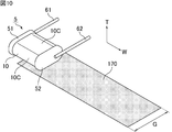
- FIG. 1 It is a perspective schematic diagram which shows an example of the film capacitor of this invention. It is a perspective schematic diagram which shows the state which disassembled the film capacitor in FIG. It is sectional drawing which shows the part corresponding to the line segment A1-A2 in FIG. It is sectional drawing which shows the part corresponding to the line segment B1-B2 in FIG. It is sectional drawing which shows the part corresponding to the line segment C1-C2 in FIG. It is a perspective schematic diagram which shows the capacitor element in FIG. It is sectional drawing which shows the part corresponding to the line segment D1-D2 in FIG. It is a perspective schematic diagram which shows the 1st method about the process of providing the release material in the manufacturing method of the film capacitor of this invention.
- the film capacitor of the present invention will be described.
- the present invention is not limited to the following configuration, and may be appropriately modified without departing from the gist of the present invention.
- a combination of a plurality of individual preferred configurations described below is also the present invention.
- Film capacitor As an example of the film capacitor of the present invention, a so-called winding type film in which a film containing a metallized film having a metal layer provided on at least one main surface of a dielectric film is wound in a laminated state.
- the capacitor will be described below.
- the film capacitor of the present invention may be a so-called laminated film capacitor in which the above films are laminated.
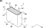
- FIG. 1 is a schematic perspective view showing an example of the film capacitor of the present invention.
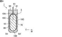
- FIG. 2 is a schematic perspective view showing a state in which the film capacitor in FIG. 1 is disassembled.
- FIG. 2 shows a state before the capacitor element with the external extraction terminal is housed in the outer case.
- FIG. 3 is a schematic cross-sectional view showing a portion corresponding to the line segments A1-A2 in FIG.
- FIG. 4 is a schematic cross-sectional view showing a portion corresponding to the line segments B1-B2 in FIG.
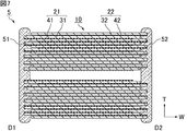
- FIG. 5 is a schematic cross-sectional view showing a portion corresponding to the line segments C1-C2 in FIG.
- the stacking direction and the width direction of the film capacitor are defined by arrows T and W, respectively, as shown in FIGS. 1, 2, 3, 4, and 5, respectively. It can be said that the winding type film capacitor has a plurality of stacking directions, but in the present specification, the direction is defined by the arrow T.
- the stacking direction T and the width direction W are orthogonal to each other.
- the film capacitor 1 is peeled off from the capacitor element 5, the first external extraction terminal 61, and the second external extraction terminal 62. It has a material 70, an outer case 80, and a filling resin 90.
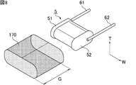
- FIG. 6 is a schematic perspective view showing the capacitor element in FIG.
- FIG. 7 is a schematic cross-sectional view showing a portion corresponding to the line segments D1-D2 in FIG.
- the capacitor element 5 includes a laminate 10, a first external electrode 51 provided on one end surface of the laminate 10 in the width direction W, and a laminate in the width direction W. It has a second external electrode 52 provided on the other end face of the ten.
- both end faces of the laminated body 10 face each other in the width direction W.
- the laminated body 10 has an upper surface 10A, a lower surface 10B, and a side surface 10C in addition to both end faces provided with the first external electrode 51 and the second external electrode 52.
- the upper surface 10A of the laminated body 10 is located on the opening 81 side of the outer case 80.
- the lower surface 10B of the laminated body 10 faces the upper surface 10A and is located on the bottom surface side of the outer case 80.
- the side surfaces 10C of the laminated body 10 are a pair of surfaces facing each other in the stacking direction T. As shown in FIG. 4, the upper surface 10A and the lower surface 10B of the laminated body 10 may be rounded.
- the laminated body 10 is a wound body in which the first metallized film 21 and the second metallized film 22 are wound in a state of being laminated in the stacking direction T.
- the film capacitor 1 is a winding type film capacitor having a laminated body 10 which is also such a winding body.
- the cross-sectional shape of the laminated body 10 is pressed into a flat shape such as an ellipse or an oval, and the cross-sectional shape of the laminated body 10 is a perfect circle. It is preferable that the shape has a small thickness.
- the capacitor element 5 may have a columnar winding shaft.
- the winding shaft is arranged on the central axis of the first metallized film 21 and the second metallized film 22 in the wound state, and the first metallized film 21 and the second metallized film 22 are arranged. It serves as a winding shaft when winding 22.
- the first metallized film 21 has a first metal layer 41 provided on one main surface of the first dielectric film 31.
- the first metal layer 41 is provided so as to reach one side edge of the first metallized film 21 and not reach the other side edge of the first metallized film 21 in the width direction W.
- the second metallized film 22 is one in which a second metal layer 42 is provided on one main surface of the second dielectric film 32.
- the second metal layer 42 is provided so as not to reach one side edge of the second metallized film 22 but to reach the other side edge of the second metallized film 22 in the width direction W.
- the end portion of the first metal layer 41 on the side reaching the side edge of the first metallized film 21 is exposed on one end surface of the laminated body 10, and the second metal layer 42
- the adjacent first metallized film 21 and the second metallized film 22 are arranged so that the end portion on the side reaching the side edge of the second metallized film 22 is exposed to the other end surface of the laminated body 10. It is deviated in the width direction W.
- the laminate 10 is wound in a state where the first metallized film 21 and the second metallized film 22 are laminated in the lamination direction T, the first metal layer 41 and the first dielectric material are formed. It can also be said that the film 31, the second metal layer 42, and the second dielectric film 32 are wound in a state of being laminated in order in the stacking direction T.
- the first metallized film 21 is inside the second metallized film 22, the first metal layer 41 is inside the first dielectric film 31, and the second metal layer 42 is inside.
- the first metallized film 21 and the second metallized film 22 are wound in a laminated state in the stacking direction T so as to be inside the second dielectric film 32.
- the second metal layer 42 may be provided not on one main surface of the second dielectric film 32 but on the other main surface of the first dielectric film 31.
- the first metal layer 41 is provided on one main surface of the first dielectric film 31, and the second metal layer 42 is provided on the other main surface.
- the metallized film and the second dielectric film 32 are wound in a state of being laminated in the stacking direction T.
- the first dielectric film 31 and the second dielectric film 32 each contain a curable resin as a main component.
- the principal component means a component having the largest weight percentage, and preferably means a component having a weight percentage larger than 50% by weight.
- the curable resin may be a thermosetting resin or a photocurable resin.
- the thermosetting resin means a resin that can be cured by heat, and does not limit the curing method. Therefore, as long as the resin can be cured by heat, the thermosetting resin also includes a resin cured by a method other than heat (for example, light, electron beam, etc.). Further, depending on the material, the reaction may be started due to the reactivity of the material itself, and a thermosetting resin is also used if the material is cured without necessarily applying heat or light from the outside. The same applies to the photocurable resin, and the curing method is not limited as long as the resin can be cured by light.
- the curable resin may have at least one of urethane bond and urea bond, and may not have both urethane bond and urea bond.
- the presence of urethane bond and / or urea bond can be confirmed by using a Fourier transform infrared spectrophotometer (FT-IR).
- FT-IR Fourier transform infrared spectrophotometer
- the curable resin is preferably composed of a cured product of the first organic material and the second organic material.
- a cured product include a cured product obtained by reacting a hydroxyl group (OH group) contained in the first organic material with an isocyanate group (NCO group) contained in the second organic material.
- NCO group isocyanate group
- the first dielectric film 31 and the second dielectric film 32 may each contain one of a hydroxyl group and an isocyanate group, or may contain both a hydroxyl group and an isocyanate group. ..
- the presence of hydroxyl groups and / or isocyanate groups can be confirmed using a Fourier transform infrared spectrophotometer.
- the first organic material is preferably a polyol having a plurality of hydroxyl groups in the molecule.
- the polyol include polyvinyl acetal such as polyvinyl acetal acetal, polyether polyol such as phenoxy resin, polyester polyol and the like.
- the first organic material a plurality of types of organic materials may be used in combination.
- the second organic material is preferably an isocyanate compound, an epoxy resin, or a melamine resin having a plurality of functional groups in the molecule.
- a plurality of types of organic materials may be used in combination.
- isocyanate compound examples include aromatic polyisocyanates such as diphenylmethane diisocyanate (MDI) and tolylene diisocyanate (TDI), and aliphatic polyisocyanates such as hexamethylene diisocyanate (HDI).
- aromatic polyisocyanates such as diphenylmethane diisocyanate (MDI) and tolylene diisocyanate (TDI)
- aliphatic polyisocyanates such as hexamethylene diisocyanate (HDI).
- the isocyanate compound may be a modified product of these polyisocyanates, for example, a modified product having carbodiimide, urethane, or the like.
- the epoxy resin is not particularly limited as long as it has an epoxy ring, and examples thereof include a bisphenol A type epoxy resin, a biphenyl skeleton epoxy resin, a cyclopentadiene skeleton epoxy resin, and a naphthalene skeleton epoxy resin.
- the melamine resin is not particularly limited as long as it is an organic nitrogen compound having a triazine ring at the center of the structure and three amino groups around it, and examples thereof include alkylated melamine resins.
- the melamine resin may be a modified form of melamine.
- the first dielectric film 31 and the second dielectric film 32 are preferably formed by forming a resin solution containing the first organic material and the second organic material into a film, and then heat-treating and curing the resin solution. It is made.
- the first dielectric film 31 and the second dielectric film 32 may each contain a vapor-deposited polymer film as a main component.
- the vapor-deposited polymerized film may have at least one of a urethane bond and a urea bond, or may not have both a urethane bond and a urea bond.
- the thin-film deposition polymer film refers to a film formed by a thin-film deposition polymerization method, and is basically included in a curable resin.
- the first dielectric film 31 and the second dielectric film 32 may each contain a thermoplastic resin as a main component.
- thermoplastic resin examples include polypropylene, polyether sulfone, polyetherimide, polyarylate and the like.
- Each of the first dielectric film 31 and the second dielectric film 32 has uncured portions of starting materials such as silicone resin, first organic material and second organic material as components other than the main components. Etc. may be contained.
- the first dielectric film 31 and the second dielectric film 32 may each contain additives for adding various functions.
- the additive include a leveling agent for imparting smoothness.
- the additive preferably has a functional group that reacts with a hydroxyl group and / or an isocyanate group, and forms a part of the crosslinked structure of the cured product.
- examples of such an additive include a resin having at least one functional group selected from the group consisting of a hydroxyl group, an epoxy group, a silanol group, and a carboxyl group.
- compositions of the first dielectric film 31 and the second dielectric film 32 may be different from each other, but are preferably the same.
- the thickness of the first dielectric film 31 and the second dielectric film 32 is preferably 0.5 ⁇ m or more and 5 ⁇ m or less, respectively.
- the thicknesses of the first dielectric film 31 and the second dielectric film 32 may be different from each other, but are preferably the same.
- the thickness of the first dielectric film 31 and the second dielectric film 32 can be measured using an optical film thickness meter.
- Examples of the constituent materials of the first metal layer 41 and the second metal layer 42 include metals such as aluminum, zinc, titanium, magnesium, tin, and nickel, respectively.
- compositions of the first metal layer 41 and the second metal layer 42 may be different from each other, but are preferably the same.
- the thicknesses of the first metal layer 41 and the second metal layer 42 are preferably 5 nm or more and 40 nm or less, respectively.
- the thickness of the first metal layer 41 can be specified by observing the cut surface of the first metallized film 21 in the thickness direction using a transmission electron microscope (TEM).
- the thickness of the second metal layer 42 can be specified in the same manner.
- the first external electrode 51 is provided on one end surface of the laminated body 10 and is connected to the first metal layer 41 by coming into contact with the exposed end portion of the first metal layer 41.
- the first metallized film 21 has a width with respect to the second metallized film 22. It is preferable that it protrudes in the direction W.
- the second external electrode 52 is provided on the other end surface of the laminated body 10 and is connected to the second metal layer 42 by coming into contact with the exposed end portion of the second metal layer 42.
- the second metallized film 22 has a width with respect to the first metallized film 21. It is preferable that it protrudes in the direction W.
- first external electrode 51 and the second external electrode 52 examples include metals such as zinc, aluminum, tin, and zinc-aluminum alloy.
- the first external electrode 51 and the second external electrode 52 are preferably formed by spraying a metal as described above onto one end face and the other end face of the laminate 10, respectively.
- compositions of the first external electrode 51 and the second external electrode 52 may be different from each other, but are preferably the same.
- the configuration of the laminated body 10 may be different from the configuration as shown in FIG.
- the first metal layer 41 is divided into two metal layers in the width direction W, one metal layer reaches one side edge of the first metallized film 21, and the other.
- the metal layer may be provided so as to reach the other side edge of the first metallized film 21.
- one metal layer is connected to the first external electrode 51, and the other metal layer is connected to the second external electrode 52, while the second metal layer 42 is connected. Is provided so as not to be connected to both the first external electrode 51 and the second external electrode 52, a capacitor can be formed between the first metal layer 41 and the second metal layer 42.
- the first external extraction terminal 61 is connected to the first external electrode 51.
- the first external lead-out terminal 61 may be electrically connected to the first external electrode 51 via, for example, a solder layer.
- the first external drawer terminal 61 projects from the inside of the outer case 80 toward the outside.
- connection position between the first external lead-out terminal 61 and the first external electrode 51 may be the central portion of the first external electrode 51, as described in FIG. 1 of Japanese Patent No. 4733566. It may be the end of the first external electrode 51 close to the opening 81 of the outer case 80.
- the second external extraction terminal 62 is connected to the second external electrode 52.
- the second external extraction terminal 62 may be electrically connected to the second external electrode 52, for example, via a solder layer.
- the second external drawer terminal 62 projects from the inside of the outer case 80 toward the outside.
- connection position between the second external extraction terminal 62 and the second external electrode 52 may be the central portion of the second external electrode 52, as described in FIG. 1 of Japanese Patent No. 4733566. It may be the end of the second external electrode 52 close to the opening 81 of the outer case 80.
- Examples of the constituent materials of the first external lead-out terminal 61 and the second external lead-out terminal 62 include metals such as copper, tin, and aluminum.
- compositions of the first external extraction terminal 61 and the second external extraction terminal 62 may be different from each other, but are preferably the same.
- the shape of the first external drawer terminal 61 and the second external drawer terminal 62 may be linear (rod-shaped) or plate-shaped.
- the shapes of the first external extraction terminal 61 and the second external extraction terminal 62 may be different from each other, but are preferably the same.
- the outer case 80 is provided with an opening 81 at one end and houses the capacitor element 5 inside.
- the shape of the outer case 80 is not particularly limited as long as it has an opening 81 at one end, and is, for example, a bottomed square cylinder having a square cylindrical side wall portion as shown in FIG. It may be a bottomed cylinder having a cylindrical side wall portion.
- Examples of the constituent material of the outer case 80 include metals such as aluminum, magnesium, iron, stainless steel, and copper, alloys of these metals, resins such as polybutylene terephthalate, polyphenylene sulfide, and liquid crystal polymer (LCP). ..
- the constituent material of the outer case 80 is a metal or alloy as described above, the water vapor barrier property of the outer case 80 is enhanced. Therefore, even if the film capacitor 1 is used in a high temperature and high humidity environment, the hydroxylation reaction of the first metal layer 41 and the second metal layer 42 due to the infiltration of water is less likely to proceed, and as a result, it becomes difficult to proceed. The decrease in capacitance is suppressed. On the other hand, since the conductivity of the outer case 80 is also increased, it may be necessary to take measures for insulation between the first external drawer terminal 61 and the second external drawer terminal 62 and the outer case 80.
- the outer case 80 is manufactured by, for example, impact molding or the like.
- the constituent material of the exterior case 80 is a resin composition containing a resin having high insulating properties as described above, the above-mentioned insulating measures are not required.
- the resin composition constituting the outer case 80 contains a liquid crystal polymer, the water vapor barrier property of the outer case 80 is enhanced.
- liquid crystal polymer contained in the resin composition examples include a liquid crystal polymer having a p-hydroxybenzoic acid and a 6-hydroxy-2-naphthoic acid group in the skeleton.
- a liquid crystal polymer having a polycondensate formed by using various components such as phenol, phthalic acid, and ethylene terephthalate can be used.
- classification methods such as type I, type II, and type III, but the material means the same material as the liquid crystal polymer formed from the above components.
- the content of the liquid crystal polymer in the resin composition is preferably 40% by weight or more and 95% by weight or less, and more preferably 40% by weight or more and 85% by weight or less.
- the resin composition preferably contains an inorganic filler in addition to the liquid crystal polymer.
- an inorganic filler a material having higher strength than the liquid crystal polymer can be used.
- the inorganic filler is preferably a material having a melting point higher than that of the liquid crystal polymer, and more preferably a material having a melting point of 680 ° C. or higher.
- the form of the inorganic filler is not particularly limited, and examples thereof include a form having a longitudinal direction such as a fibrous shape or a plate shape. A plurality of types of inorganic materials may be used in combination as the inorganic filler having such a form.
- the resin composition preferably contains at least one of a fibrous inorganic material and a plate-shaped inorganic material as the inorganic filler.
- the fibrous means that the relationship between the longitudinal length of the filler in the longitudinal direction and the cross-sectional diameter in the cross section perpendicular to the longitudinal direction is the longitudinal length / cross-sectional diameter ⁇ 5 (that is, the aspect ratio is It means a state of 5: 1 or more).
- the cross-sectional diameter is the longest distance between two points on the outer circumference of the cross-section. If the cross-sectional diameter differs in the longitudinal direction, the measurement is performed at the point where the cross-sectional diameter is maximum.
- the plate shape means a state in which the relationship between the cross-sectional diameter of the surface having the maximum projected area and the maximum height in the direction perpendicular to this cross-section is cross-sectional diameter / maximum height ⁇ 3. To do.
- the resin composition may contain an inorganic filler that satisfies both the fibrous and plate-like conditions described above.
- the inorganic filler contains only one type of inorganic material.
- the resin composition contains both a fibrous inorganic material and a plate-shaped inorganic material as an inorganic filler.
- the inorganic filler has a portion that is oriented toward the opening 81 from the bottom side and a portion that is oriented toward the adjacent side wall in each side wall of the side portion of the exterior case 80. It is preferable that it has and is dispersed inside the outer case 80.
- the size of the inorganic filler is preferably a size having a diameter of 5 ⁇ m or more and a length of 50 ⁇ m or more.
- the inorganic filler is dispersed throughout the outer case 80 without agglomeration.
- inorganic filler examples include inorganic materials such as glass fiber, mica, talc, various oxides, and various hydroxides.
- the content of the inorganic filler in the resin composition is preferably 5% by weight or more, more preferably 15% by weight or more. Further, from the viewpoint of ensuring the moldability of the outer case 80, the content of the inorganic filler in the resin composition is preferably 60% by weight or less.
- the content of the inorganic filler in the resin composition is measured by measuring the residual component as an inorganic component by ash content measurement or thermogravimetric analysis using a test piece having a thickness of 20 mm ⁇ 20 mm ⁇ 0.5 mm. It can be calculated from the measured initial weight and residual component weight. More specifically, based on the JIS K 7250 A method (direct ashing method), the organic material is burned and the combustion residue is measured by heating it at a high temperature until it becomes constant.
- the outer case 80 is manufactured by, for example, injection molding or the like.
- the release material 70 includes a part of the capacitor element 5, a part of the first external extraction terminal 61, and a part of the second external extraction terminal 62. It covers and. More specifically, the release material 70 covers a part of the surface of the first external electrode 51 and the second external electrode 52 located on the opening 81 side of the outer case 80. Further, the release material 70 covers the connection portion of the first external extraction terminal 61 with the first external electrode 51 and the connection portion of the second external extraction terminal 62 with the second external electrode 52. ..
- the first external extraction terminal 61 and the second external extraction terminal 62 are electrically connected to the first external electrode 51 and the second external electrode 52, respectively, via a solder layer.
- the connection portion of the first external extraction terminal 61 with the first external electrode 51 and the connection portion of the second external extraction terminal 62 with the second external electrode 52 each include a solder layer.
- the release material 70 is a connection portion between the first external electrode 51 and the first external electrode 51 in the first external extraction terminal 61, a second external electrode 52, and a second external extraction terminal 62.
- the connection portion of 2 with the external electrode 52 By covering the connection portion of 2 with the external electrode 52, the connection portion between the first external electrode 51 and the first external electrode 51 at the first external extraction terminal 61, and the second external electrode 52 , The connection portion of the second external extraction terminal 62 with the second external electrode 52 is less likely to be bound by the filling resin 90 described later. Therefore, even if the film capacitor 1 is moved to a low temperature environment or a high temperature environment, tensile stress is less likely to occur in the first external electrode 51 and the second external electrode 52. As a result, the occurrence of cracks in the first external electrode 51 and the second external electrode 52 is suppressed.
- the release material 70 does not cover at least a part of the upper surface 10A of the laminated body 10. More specifically, the release material 70 does not cover a part of the upper surface 10A of the laminated body 10, or does not cover the entire upper surface 10A of the laminated body 10.
- the release material 70 has a first external extraction terminal 61 and a second external extraction terminal 61 when the capacitor element 5 with the first external extraction terminal 62 and the second external extraction terminal 62 is viewed from the upper surface 10A side of the laminated body 10. It does not have to cover the area connecting the drawer terminal 62.
- the width of such a region is preferably equal to or greater than the width of the smaller of the widths of the first external extraction terminal 61 and the second external extraction terminal 62.
- the release material 70 does not cover at least a part of the upper surface 10A of the laminate 10, a part of the upper surface 10A comes into contact with the filling resin 90 described later. Therefore, the infiltration of water from the opening 81 of the outer case 80 into the upper surface 10A of the laminated body 10 is suppressed.
- release material 70 does not cover a part of the upper surface 10A of the laminate 10, that is, covers a part of the upper surface 10A of the laminate 10, a part of the upper surface 10A of the laminate 10 covered with the release material 70. May be in close contact with the release material 70.
- the release material 70 does not have to cover at least a part of the lower surface 10B of the laminated body 10. More specifically, the release material 70 may not cover a part of the lower surface 10B of the laminated body 10, or may not cover the entire lower surface 10B of the laminated body 10. Since the release material 70 does not cover at least a part of the lower surface 10B of the laminate 10, a part of the lower surface 10B comes into contact with the filling resin 90 described later. Therefore, the infiltration of water from the opening 81 of the outer case 80 into the lower surface 10B of the laminated body 10 is suppressed.
- the release material 70 may cover the side surface 10C of the laminate 10.
- the release material 70 can be easily fixed. Further, since the side surface 10C of the laminated body 10 is less likely to be restrained by the filling resin 90 described later, the stress generated in the laminated body 10 when the film capacitor 1 is moved to a low temperature environment or a high temperature environment is relaxed.
- release material 70 examples include a biaxially stretched polypropylene film, a polyester adhesive tape (Mylar tape), and the like.
- connection portion between the first external electrode 51 and the first external electrode 51 in the first external extraction terminal 61, the second external electrode 52, and the second external For example, a biaxially stretched polypropylene film is drawn from the first external drawing so as to cover the connection portion of the drawing terminal 62 with the second external electrode 52 and not to cover at least a part of the upper surface 10A of the laminated body 10.
- Examples thereof include a method of providing the capacitor element 5 with the terminal 61 and the second external extraction terminal 62 so as to be wound around the capacitor element 5. A specific example of the method of providing the release material 70 in this way will be described later.
- FIGS. 1, 2, 3, 4, and 5 a state in which a single capacitor element 5 is housed in a single exterior case 80 is illustrated, but is described in, for example, Patent Document 1.
- a plurality of capacitor elements 5 may be housed in a single exterior case 80.
- the release material 70 may be individually provided on the plurality of capacitor elements 5, or may be provided alone so as to bundle the plurality of capacitor elements 5.
- the thickness of the release material 70 is preferably 12 ⁇ m or more and 50 ⁇ m or less.
- the thickness of the release material 70 can be measured using an optical film thickness meter.
- the release material 70 is in at least in contact with the corner portion where the pair of side surfaces of the first external electrode 51 in the stacking direction T and the end surface in the width direction W intersect with the first external extraction terminal 61. However, it is at least not in contact with the end face of the first external electrode 51. Therefore, there is a region surrounded by the first external electrode 51, the first external extraction terminal 61, and the release material 70. Similarly, the release material 70 is in contact with at least the corner portion where the pair of side surfaces of the second external electrode 52 in the stacking direction T and the end surface in the width direction W intersect with the second external extraction terminal 62, and the second external electrode 52 is in contact with the second external electrode 52. At least not in contact with the end face of the external electrode 52.
- the filling resin 90 is filled from the opening 81 of the outer case 80, at least a part of the upper surface 10A of the laminate 10 not covered with the release material 70 is connected to the first external electrode 51. It enters the region surrounded by the first external extraction terminal 61 and the release material 70, and the region surrounded by the second external electrode 52, the second external extraction terminal 62, and the release material 70. Therefore, as shown in FIG. 5, in the film capacitor 1, the filled resin 90 is surrounded by the first external electrode 51, the first external extraction terminal 61, and the release material 70, and the second outer surface. It is provided in a region surrounded by the electrode 52, the second external extraction terminal 62, and the release material 70.
- the release material 70 does not have to cover at least a part of the lower surface 10B of the laminate 10, but in this case, the filling resin 90 is the lower surface 10B of the laminate 10 not covered with the release material 70.
- the filling resin 90 is provided in the area surrounded by the first external electrode 51, the first external extraction terminal 61, and the release material 70, so that the first external electrode 51 comes into contact with the filling resin 90. Therefore, the infiltration of water from the opening 81 of the outer case 80 into the first external electrode 51 is suppressed.
- the filling resin 90 is provided in the area surrounded by the second external electrode 52, the second external extraction terminal 62, and the release material 70, so that the second external electrode 52 comes into contact with the filling resin 90. Therefore, the infiltration of water from the opening 81 of the outer case 80 into the second external electrode 52 is suppressed.
- connection portion of the first external extraction terminal 61 with the first external electrode 51 and the connection portion of the second external extraction terminal 62 with the second external electrode 52 are small, in a conventional film capacitor, When a load is applied to the first external extraction terminal 61 and the second external extraction terminal 62, the first external extraction terminal 61 is separated from the first external electrode 51, and the second external extraction terminal 62 is the second. There is a risk of separation from the external electrode 52 of 2.
- the region surrounded by the first external electrode 51, the first external extraction terminal 61 and the release material 70, and the second external electrode 52 and the second external extraction terminal Since the filling resin 90 is provided in the region surrounded by the release material 70, the connection portion between the first external electrode 51 and the first external extraction terminal 61 is reinforced, and the second external electrode 52 and the second external electrode 52 are reinforced.
- the connection portion with the second external extraction terminal 62 is reinforced.
- the filling resin 90 is filled through the opening 81 of the outer case 80, it also enters the region between the release material 70 and the outer case 80. Therefore, as shown in FIG. 5, in the film capacitor 1, the filling resin 90 is provided in the region between the release material 70 and the outer case 80.
- the filling resin 90 may be provided in the region between the side surface 10C of the laminate 10 and the release material 70.
- the filling resin 90 may be provided in the region between the side surface 10C of the laminated body 10 and the release material 70.
- the side surface 10C of the laminated body 10 comes into contact with the filling resin 90. Therefore, the infiltration of water from the opening 81 of the outer case 80 into the side surface 10C of the laminated body 10 is suppressed.
- the filling resin 90 it is preferable to appropriately select a resin having low moisture permeability from the viewpoint of suppressing the infiltration of water into the capacitor element 5, and examples thereof include epoxy resin, silicone resin, and urethane resin.
- examples of the epoxy resin curing agent include amine curing agents and imidazole curing agents.
- a reinforcing agent may be added to the filling resin 90 for the purpose of improving the strength.
- the reinforcing agent include silica, alumina and the like.
- the thickness of the filling resin 90 in the opening 81 of the outer case 80 is large.
- the thickness of the filling resin 90 in the opening 81 of the outer case 80 is preferably sufficiently large within an allowable range of the volume (physique) of the entire film capacitor 1, specifically, preferably 2 mm or more, more preferably 4 mm. That is all.
- the thickness of the filling resin 90 with respect to the capacitor element 5 can be adjusted to the bottom surface on the opening 81 side of the exterior case 80. It is preferable to make it larger than the side.
- the thickness of the filling resin 90 can be measured using a soft X-ray device if it is in a non-destructive state, and can be measured using a length measuring device such as a caliper if it is in a broken state.
- the relationship between the height of the filling resin 90 and the height of the outer case 80 is such that the thickness of the filling resin 90 at the opening 81 of the outer case 80 may be made as large as possible, and may be up to the position on the inner side of the outer case 80. It may be full, or it may be slightly overflowed due to surface tension.
- the film capacitor of the present invention is manufactured by, for example, the following method.
- a resin solution is prepared by mixing the above-mentioned first organic material, second organic material, additives and the like. Then, the obtained resin solution is formed into a film and then heat-treated and cured to produce a first dielectric film and a second dielectric film.
- the first metal layer is formed.
- a metal such as aluminum, zinc, titanium, magnesium, tin, or nickel
- a second metal layer is formed by depositing a metal such as aluminum, zinc, titanium, magnesium, tin, or nickel on one main surface of the second dielectric film to form a second metal layer. Make a metallized film. At this time, the second metal layer is formed so as not to reach one side edge of the second metallized film in the width direction but to reach the other side edge of the second metallized film.
- a metal such as aluminum, zinc, titanium, magnesium, tin, or nickel
- the second metal layer may be formed not on one main surface of the second dielectric film but on the other main surface of the first dielectric film.
- the first metal layer is formed so as to reach one side edge of the metallized film and not reach the other side edge of the metallized film, and one side edge of the metallized film is formed.
- the second metal layer may be formed so as to reach the other side edge of the metallized film without reaching.
- the first metallized film and the second metallized film are stacked in a state of being shifted by a predetermined distance in the width direction, and then wound to produce a laminated body (winding body). If necessary, the obtained laminate may be sandwiched from a direction perpendicular to the width direction and pressed into an elliptical cylinder shape.
- the first external electrode is connected to the first metal layer by spraying a metal such as zinc, aluminum, tin, or zinc-aluminum alloy onto one end face of the laminate.
- the second external electrode is formed so as to be connected to the second metal layer by spraying a metal such as zinc, aluminum, tin, or zinc-aluminum alloy onto the other end face of the laminate. To do.
- the capacitor element is manufactured.
- the first external lead-out terminal is provided so as to be connected to the first external electrode, for example, via a solder layer. Further, the second external extraction terminal is provided so as to be connected to the second external electrode via, for example, a solder layer.
- the constituent materials of the first external lead-out terminal and the second external lead-out terminal are, for example, metals such as copper, tin, and aluminum, respectively.
- a biaxially stretched polypropylene film is provided so as to be wrapped around a capacitor element having a first external extraction terminal and a second external extraction terminal so as to cover and not cover at least a part of the upper surface of the laminate.
- FIGS. 8 and 9 are schematic perspective views showing a first method for providing a release material in the method for manufacturing a film capacitor of the present invention.
- a shrink film 170 such as a biaxially stretched polypropylene film is formed into a tubular shape by heat-sealing the ends with a heat seal.
- the shrink film 170 will later become the release material 70.
- the width G of the shrink film 170 is the direction of the capacitor element 5 in the direction orthogonal to the stacking direction T and the width direction W (in FIG. 8, the direction in which the first external extraction terminal 61 and the second external extraction terminal 62 extend). It is preferably larger than the length.
- the capacitor element 5 with the first external extraction terminal 61 and the second external extraction terminal 62 provided with the release material 70 is formed. obtain. More specifically, in the connection portion between the first external electrode 51 and the first external electrode 51 in the first external extraction terminal 61, the second external electrode 52, and the second external extraction terminal 62.
- the release material 70 is provided so as to cover the connection portion with the second external electrode 52 and not to cover at least a part of the upper surface 10A of the laminated body 10.
- the release material 70 has traces of the heat seal of the shrink film 170 as described above.
- the trace of such a heat seal exists in the release material 70 at a position facing the side surface 10C of the laminated body 10, for example.
- the shape of the heat seal may be point-shaped or planar.
- FIGS. 10 and 11 are schematic perspective views showing a second method for a step of providing a release material in the method for manufacturing a film capacitor of the present invention.
- a shrink film 170 such as a biaxially stretched polypropylene film is fixed to the side surface 10C of the laminated body 10 of the capacitor element 5 by heat fusion by heat sealing.
- the shape of the heat seal may be point-shaped or planar.
- the width G of the shrink film 170 is the direction of the capacitor element 5 in the direction orthogonal to the stacking direction T and the width direction W (in FIG. 10, the direction in which the first external extraction terminal 61 and the second external extraction terminal 62 extend). It is preferably larger than the length.
- the shrink film 170 is wound around the capacitor element 5 with the first external extraction terminal 61 and the second external extraction terminal 62 so as to cover the capacitor element 5.
- the shrink film 170 may be wound for one round or for two or more turns.
- the other end of the shrink film 170 is fixed to a part of the shrink film 170, for example, a position facing the side surface 10C of the laminate 10 in the shrink film 170 by heat fusion by heat sealing. ..
- the shape of the heat seal may be point-shaped or planar.
- the capacitor element 5 with the first external extraction terminal 61 and the second external extraction terminal 62 provided with the release material 70 is formed. obtain. More specifically, in the connection portion between the first external electrode 51 and the first external electrode 51 in the first external extraction terminal 61, the second external electrode 52, and the second external extraction terminal 62.
- the release material 70 is provided so as to cover the connection portion with the second external electrode 52 and not to cover at least a part of the upper surface 10A of the laminated body 10.
- an exterior case having an opening at one end is produced by injection molding using a resin composition containing a highly insulating resin such as polybutylene terephthalate, polyphenylene sulfide, and a liquid crystal polymer.
- a resin composition containing a highly insulating resin such as polybutylene terephthalate, polyphenylene sulfide, and a liquid crystal polymer.
- an outer case having an opening at one end may be produced by impact molding using a metal such as aluminum, magnesium, iron, stainless steel, or copper, or an alloy thereof.
- the capacitor element with the first external extraction terminal and the second external extraction terminal provided with the release material is housed inside the outer case.
- a filling resin such as an epoxy resin, a silicone resin, or a urethane resin is filled through the opening of the outer case, and the capacitor element is buried.
- the filling resin is formed from at least a part of the upper surface of the laminate not covered with the release material, a region surrounded by the first external electrode, the first external extraction terminal, and the release material, and the second. It enters the area surrounded by the external electrode, the second external extraction terminal, and the release material.
- the filling resin also enters the area between the release material and the outer case.
- the filling resin contains a region surrounded by the first external electrode, the first external extraction terminal, and the release material, a region surrounded by the second external electrode, the second external extraction terminal, and the release material, and It will be provided in the area between the release material and the outer case.
- the film capacitor of the present invention is manufactured.
- Example 1 The film capacitor of Example 1 was manufactured by the following method.
- a resin solution was prepared by mixing phenoxy resin, which is a bisphenol A type epoxy resin as a first organic material, and diphenylmethane diisocyanate, which is a second organic material, at a weight ratio of 7: 3. Then, the obtained resin solution was formed into a film and then heat-treated and cured to prepare a first dielectric film and a second dielectric film. The thickness of the first dielectric film and the second dielectric film was 3 ⁇ m.
- the first metal layer was formed so as to reach one side edge of the first metallized film and not reach the other side edge of the first metallized film.
- the thickness of the first metal layer was 20 nm.
- a second metallized film was produced by depositing aluminum on one main surface of the second dielectric film to form a second metal layer. At this time, the second metal layer was formed so as not to reach one side edge of the second metallized film in the width direction but to reach the other side edge of the second metallized film.
- the thickness of the second metal layer was 20 nm.
- the first metallized film and the second metallized film were laminated in a state of being shifted by a predetermined distance in the width direction, and then wound to prepare a laminated body (winding body). Then, the obtained laminate was sandwiched from a direction perpendicular to the width direction and pressed into an elliptical cylinder shape.
- the second external electrode was formed so as to be connected to the second metal layer by spraying zinc on the other end face of the laminated body.
- the capacitor element was manufactured.
- the first external lead-out terminal is provided so as to be connected to the first external electrode via a solder layer. Further, the second external lead-out terminal is provided so as to be connected to the second external electrode via the solder layer.
- the first external lead-out terminal and the second external lead-out terminal were each made of copper and had a tin-plated surface.
- connection portion between the first external electrode and the first external electrode in the first external extraction terminal, the second external electrode, and the second in the second external extraction terminal A biaxially stretched polypropylene film as a release material is provided as a first external extraction terminal and a second external extraction terminal so as to cover the connection portion with the external electrode and not to cover at least a part of the upper surface of the laminate. It was provided in the attached capacitor element.
- the heat treatment for shrinking the shrink film was carried out at 120 ° C. for 3 seconds using a hot air gun or a dryer.
- the thickness of the release material was 50 ⁇ m.
- the filling resin contains a region surrounded by the first external electrode, the first external extraction terminal, and the release material, a region surrounded by the second external electrode, the second external extraction terminal, and the release material, and It was provided in the area between the release material and the outer case.
- the film capacitor of Example 1 was manufactured for 5 samples.
- Comparative Example 1 A film capacitor of Comparative Example 1 was produced for 5 samples in the same manner as the film capacitor of Example 1 except that the step of providing the release material was not performed.
- Example 1 and Comparative Example 1 were subjected to a heat cycle test in a temperature range of ⁇ 40 ° C. or higher and 125 ° C. or lower.
- one cycle was defined as a cycle in which the film capacitor was transferred from a low temperature environment of ⁇ 40 ° C. to a high temperature environment of 125 ° C. and then from a high temperature environment of 125 ° C. to a low temperature environment of ⁇ 40 ° C.
- ESR equivalent series resistance
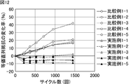
- Example 12 is a graph showing the measurement results of the rate of change of the equivalent series resistance with respect to the film capacitors of Example 1 and Comparative Example 1.
- Example 1-1 five samples of the film capacitor of Example 1 are used in "Example 1-1", “Example 1-2", “Example 1-3", “Example 1-4", and “Example 1-4". It is shown as “Example 1-5".
- 5 samples of the film capacitor of Comparative Example 1 were used as "Comparative Example 1-1", “Comparative Example 1-2”, “Comparative Example 1-3", “Comparative Example 1-4", and “Comparative Example 1". It is shown as -5 ".
- the equivalent series resistance before and after the heat cycle test at a predetermined number of cycles was measured using the LCR meter "ZM2371" manufactured by NF Circuit Design Block, and based on the following formula (F). Calculated.
- the measurement conditions for the equivalent series resistance were a measurement frequency of 10 kHz and a measurement voltage of 2 V. 100 x ["Equivalent series resistance after heat cycle test"-"Equivalent series resistance before heat cycle test”] / "Equivalent series resistance before heat cycle test” (F)
- the equivalent series resistance is stable even if the number of cycles is increased, and the occurrence of cracks in the first external electrode and the second external electrode is suppressed. It turned out that.
- the rate of change of the equivalent series resistance increased as the number of cycles increased, and the occurrence of cracks in the first external electrode and the second external electrode was not suppressed. It was.
Landscapes
- Engineering & Computer Science (AREA)
- Power Engineering (AREA)
- Microelectronics & Electronic Packaging (AREA)
- Manufacturing & Machinery (AREA)
- Fixed Capacitors And Capacitor Manufacturing Machines (AREA)
Abstract
A film capacitor 1 of the present invention comprises: a capacitor element 5 including a stack 10 and a pair of external electrodes (a first external electrode 51 and a second external electrode 52) provided on both end surfaces, in a width direction W perpendicular to a stacking direction T, of the stack 10, the stack 10 having films stacked therein in the stacking direction T, the films including a metalized film (a first metalized film 21 and a second metalized film 22) comprising a dielectric film (a first dielectric film 31 and a second dielectric film 32) with a metal layer (a first metal layer 41 and a second metal layer 42) provided on a major surface thereof; external lead-out terminals (a first external lead-out terminal 61 and a second external lead-out terminal 62) connected to the external electrodes (the first external electrode 51 and the second external electrode 52); a separating material 70 covering a part of the capacitor element 5 and a part of the external lead-out terminals (the first external lead-out terminal 61 and the second external lead-out terminal 62); an exterior case 80 having an opening 81 in one end and accommodating the capacitor element 5; and a filler resin 90 with which the exterior case 80 is filled and in which the capacitor element 5 is buried. The stack 10 has an upper surface 10A positioned on the opening 81 side of the exterior case 80. The separating material 70 covers portions of the external lead-out terminals (the first external lead-out terminal 61 and the second external lead-out terminal 62) that are connected to the external electrodes (the first external electrode 51 and the second external electrode 52) and the external electrodes (the first external electrode 51 and the second external electrode 52), and does not cover at least a part of the upper surface 10A of the stack 10. The filler resin 90 is provided in a region enclosed by the external electrodes (the first external electrode 51 and the second external electrode 52), the external lead-out terminals (the first external lead-out terminal 61 and the second external lead-out terminal 62), and the separating material 70, and in a region between the separating material 70 and the exterior case 80.
Description
本発明は、フィルムコンデンサに関する。
The present invention relates to a film capacitor.
フィルムコンデンサは、誘電体フィルムの表面に金属層が設けられた金属化フィルムが巻回又は積層されたコンデンサ素子を有している。このようなコンデンサ素子は、例えば、2枚の金属化フィルムを重ねて巻回又は積層した後、その両端面上に一対の外部電極を形成することにより作製される。そして、外部電極と接続される外部引き出し端子を形成した後、コンデンサ素子を外装ケースに収納し、充填樹脂を外装ケース内に充填することがある。
The film capacitor has a capacitor element in which a metallized film having a metal layer provided on the surface of a dielectric film is wound or laminated. Such a capacitor element is manufactured, for example, by laminating or laminating two metallized films and then forming a pair of external electrodes on both end faces thereof. Then, after forming the external lead-out terminal connected to the external electrode, the capacitor element may be housed in the outer case, and the filling resin may be filled in the outer case.
このようなフィルムコンデンサを低温環境に移行させると、金属化フィルムの積層体(巻回体も含む)の線膨張係数が充填樹脂の線膨張係数よりも大きいため、外部電極が周囲の充填樹脂に拘束された状態で、金属化フィルムの積層体が収縮しようとする。そのため、外部電極に引張応力が生じ、クラックが発生してしまう。
When such a film capacitor is moved to a low temperature environment, the linear expansion coefficient of the metallized film laminate (including the wound body) is larger than the linear expansion coefficient of the filling resin, so that the external electrode becomes the surrounding filling resin. In the restrained state, the laminate of the metallized film tries to shrink. Therefore, tensile stress is generated in the external electrode, and cracks occur.
一方、フィルムコンデンサを低温環境から高温環境に移行させると、外部電極の周囲の充填樹脂及び外装ケースが金属化フィルムの積層体よりも先に膨張し始める。そのため、外部電極に引張応力が生じ、クラックが発生してしまう。
On the other hand, when the film capacitor is moved from the low temperature environment to the high temperature environment, the filling resin around the external electrode and the outer case begin to expand before the metallized film laminate. Therefore, tensile stress is generated in the external electrode, and cracks occur.
以上のように、フィルムコンデンサにおいては、広い温度範囲で使用したときに外部電極にクラックが発生するという問題がある。特に、自動車等の車載用途においては、高い信頼性が広い温度範囲で求められているため、上記の問題を解決することが重要視されている。
As described above, the film capacitor has a problem that cracks occur in the external electrode when used in a wide temperature range. In particular, in in-vehicle applications such as automobiles, high reliability is required in a wide temperature range, and therefore, it is important to solve the above problems.
上記の問題に対して、特許文献1には、上端面が開放されたケースと、このケース内に収納される、金属化フィルムを使用して両端にメタリコン電極を設けた単数又は複数のコンデンサ素子と、メタリコン電極に接続した外部引き出し端子と、ケース内に充填されたコンデンサ素子を埋没させる樹脂組成物とを備え、メタリコン電極を剥離材で被覆した、金属化フィルムコンデンサが開示されている。
In response to the above problem, Patent Document 1 describes a case in which the upper end surface is open and a single or a plurality of capacitor elements housed in the case in which metallized films are used and metallikon electrodes are provided at both ends. Disclosed is a metallized film capacitor comprising an external lead-out terminal connected to a metallikon electrode and a resin composition for burying a capacitor element filled in a case, and the metallikon electrode coated with a release material.
一方、フィルムコンデンサの高い信頼性を実現するためには、外部電極への水分の浸入を抑制することも重要である。これに対して、特許文献1に記載の金属化フィルムコンデンサでは、メタリコン電極が剥離材で被覆されているが、外部電極への水分の浸入を抑制する点で改善の余地がある。
On the other hand, in order to realize high reliability of the film capacitor, it is also important to suppress the infiltration of water into the external electrode. On the other hand, in the metallized film capacitor described in Patent Document 1, the metallikon electrode is coated with a release material, but there is room for improvement in suppressing the infiltration of water into the external electrode.
本発明は、上記の問題を解決するためになされたものであり、外部電極でのクラックの発生が抑制されつつ、外部電極への水分の浸入が抑制されたフィルムコンデンサを提供することを目的とするものである。
The present invention has been made to solve the above problems, and an object of the present invention is to provide a film capacitor in which the occurrence of cracks in an external electrode is suppressed and the infiltration of water into the external electrode is suppressed. Is what you do.
本発明のフィルムコンデンサは、誘電体フィルムの主面上に金属層が設けられた金属化フィルムを含むフィルムが積層方向に積層された積層体と、上記積層方向と直交する幅方向における上記積層体の両端面上に設けられた一対の外部電極と、を有するコンデンサ素子と、上記外部電極と接続された外部引き出し端子と、上記コンデンサ素子の一部及び上記外部引き出し端子の一部を覆う剥離材と、一端に開口が設けられ、上記コンデンサ素子を内部に収納する外装ケースと、上記外装ケース内に充填され、上記コンデンサ素子を埋没させる充填樹脂と、を備え、上記積層体は、上記外装ケースの上記開口側に位置する上面を有し、上記剥離材は、上記外部引き出し端子における上記外部電極との接続部と上記外部電極とを覆い、かつ、上記積層体の上記上面の少なくとも一部を覆わず、上記充填樹脂は、上記外部電極と上記外部引き出し端子と上記剥離材とで囲まれる領域、及び、上記剥離材と上記外装ケースとの間の領域に設けられる、ことを特徴とする。
The film capacitor of the present invention is a laminate in which a film containing a metallized film having a metal layer provided on a main surface of a dielectric film is laminated in the lamination direction, and the laminate in a width direction orthogonal to the lamination direction. A release material that covers a capacitor element having a pair of external electrodes provided on both end surfaces of the capacitor element, an external lead-out terminal connected to the external electrode, a part of the capacitor element, and a part of the external lead-out terminal. An outer case having an opening at one end and accommodating the capacitor element inside, and a filling resin filled in the outer case and burying the capacitor element are provided, and the laminate is the outer case. The release material has an upper surface located on the opening side of the above, covers the connection portion of the external extraction terminal with the external electrode and the external electrode, and covers at least a part of the upper surface of the laminate. The filler is not covered and is provided in a region surrounded by the external electrode, the external extraction terminal, and the release material, and in a region between the release material and the outer case.
本発明によれば、外部電極でのクラックの発生が抑制されつつ、外部電極への水分の浸入が抑制されたフィルムコンデンサを提供できる。
According to the present invention, it is possible to provide a film capacitor in which the occurrence of cracks in the external electrode is suppressed and the infiltration of water into the external electrode is suppressed.
以下、本発明のフィルムコンデンサについて説明する。なお、本発明は、以下の構成に限定されるものではなく、本発明の要旨を逸脱しない範囲において適宜変更されてもよい。また、以下において記載する個々の好ましい構成を複数組み合わせたものもまた本発明である。
Hereinafter, the film capacitor of the present invention will be described. The present invention is not limited to the following configuration, and may be appropriately modified without departing from the gist of the present invention. In addition, a combination of a plurality of individual preferred configurations described below is also the present invention.
[フィルムコンデンサ]
本発明のフィルムコンデンサの一例として、誘電体フィルムの少なくとも一方の主面上に金属層が設けられた金属化フィルムを含むフィルムが積層された状態で巻回されてなる、いわゆる巻回型のフィルムコンデンサを以下に説明する。本発明のフィルムコンデンサは、上記フィルムが積層されてなる、いわゆる積層型のフィルムコンデンサであってもよい。 [Film capacitor]
As an example of the film capacitor of the present invention, a so-called winding type film in which a film containing a metallized film having a metal layer provided on at least one main surface of a dielectric film is wound in a laminated state. The capacitor will be described below. The film capacitor of the present invention may be a so-called laminated film capacitor in which the above films are laminated.
図1は、本発明のフィルムコンデンサの一例を示す斜視模式図である。図2は、図1中のフィルムコンデンサを分解した状態を示す斜視模式図である。図2は、外部引き出し端子付きのコンデンサ素子が外装ケースに収納される前の状態を示している。図3は、図1中の線分A1-A2に対応する部分を示す断面模式図である。図4は、図1中の線分B1-B2に対応する部分を示す断面模式図である。図5は、図1中の線分C1-C2に対応する部分を示す断面模式図である。
FIG. 1 is a schematic perspective view showing an example of the film capacitor of the present invention. FIG. 2 is a schematic perspective view showing a state in which the film capacitor in FIG. 1 is disassembled. FIG. 2 shows a state before the capacitor element with the external extraction terminal is housed in the outer case. FIG. 3 is a schematic cross-sectional view showing a portion corresponding to the line segments A1-A2 in FIG. FIG. 4 is a schematic cross-sectional view showing a portion corresponding to the line segments B1-B2 in FIG. FIG. 5 is a schematic cross-sectional view showing a portion corresponding to the line segments C1-C2 in FIG.
本明細書中、フィルムコンデンサにおける積層方向及び幅方向を、図1、図2、図3、図4、及び、図5に示すように、各々、矢印T及び矢印Wで定められる方向とする。なお、巻回型のフィルムコンデンサでは、積層方向が複数存在するとも言えるが、本明細書中では矢印Tで定められる方向とする。ここで、積層方向Tと幅方向Wとは、互いに直交している。
In the present specification, the stacking direction and the width direction of the film capacitor are defined by arrows T and W, respectively, as shown in FIGS. 1, 2, 3, 4, and 5, respectively. It can be said that the winding type film capacitor has a plurality of stacking directions, but in the present specification, the direction is defined by the arrow T. Here, the stacking direction T and the width direction W are orthogonal to each other.
図1、図2、図3、図4、及び、図5に示すように、フィルムコンデンサ1は、コンデンサ素子5と、第1の外部引き出し端子61と、第2の外部引き出し端子62と、剥離材70と、外装ケース80と、充填樹脂90と、を有している。
As shown in FIGS. 1, 2, 3, 4, and 5, the film capacitor 1 is peeled off from the capacitor element 5, the first external extraction terminal 61, and the second external extraction terminal 62. It has a material 70, an outer case 80, and a filling resin 90.
<コンデンサ素子>
図6は、図2中のコンデンサ素子を示す斜視模式図である。図7は、図6中の線分D1-D2に対応する部分を示す断面模式図である。図6及び図7に示すように、コンデンサ素子5は、積層体10と、幅方向Wにおける積層体10の一方の端面上に設けられた第1の外部電極51と、幅方向Wにおける積層体10の他方の端面上に設けられた第2の外部電極52と、を有している。ここで、積層体10の両端面は、幅方向Wにおいて互いに対向している。 <Capacitor element>
FIG. 6 is a schematic perspective view showing the capacitor element in FIG. FIG. 7 is a schematic cross-sectional view showing a portion corresponding to the line segments D1-D2 in FIG. As shown in FIGS. 6 and 7, thecapacitor element 5 includes a laminate 10, a first external electrode 51 provided on one end surface of the laminate 10 in the width direction W, and a laminate in the width direction W. It has a second external electrode 52 provided on the other end face of the ten. Here, both end faces of the laminated body 10 face each other in the width direction W.
図6は、図2中のコンデンサ素子を示す斜視模式図である。図7は、図6中の線分D1-D2に対応する部分を示す断面模式図である。図6及び図7に示すように、コンデンサ素子5は、積層体10と、幅方向Wにおける積層体10の一方の端面上に設けられた第1の外部電極51と、幅方向Wにおける積層体10の他方の端面上に設けられた第2の外部電極52と、を有している。ここで、積層体10の両端面は、幅方向Wにおいて互いに対向している。 <Capacitor element>
FIG. 6 is a schematic perspective view showing the capacitor element in FIG. FIG. 7 is a schematic cross-sectional view showing a portion corresponding to the line segments D1-D2 in FIG. As shown in FIGS. 6 and 7, the
積層体10は、第1の外部電極51及び第2の外部電極52が設けられた両端面以外に、上面10Aと、下面10Bと、側面10Cと、を有している。図3及び図4に示すように、コンデンサ素子5が外装ケース80に収納された状態で見たとき、積層体10の上面10Aは、外装ケース80の開口81側に位置している。積層体10の下面10Bは、上面10Aと対向しており、外装ケース80の底面側に位置している。積層体10の側面10Cは、積層方向Tにおいて対向する一対の面である。図4に示すように、積層体10の上面10A及び下面10Bは、丸みを帯びていてもよい。
The laminated body 10 has an upper surface 10A, a lower surface 10B, and a side surface 10C in addition to both end faces provided with the first external electrode 51 and the second external electrode 52. As shown in FIGS. 3 and 4, when the capacitor element 5 is housed in the outer case 80, the upper surface 10A of the laminated body 10 is located on the opening 81 side of the outer case 80. The lower surface 10B of the laminated body 10 faces the upper surface 10A and is located on the bottom surface side of the outer case 80. The side surfaces 10C of the laminated body 10 are a pair of surfaces facing each other in the stacking direction T. As shown in FIG. 4, the upper surface 10A and the lower surface 10B of the laminated body 10 may be rounded.
図7に示すように、積層体10は、第1の金属化フィルム21及び第2の金属化フィルム22が積層方向Tに積層された状態で巻回された巻回体である。フィルムコンデンサ1は、このような巻回体でもある積層体10を有する巻回型のフィルムコンデンサである。
As shown in FIG. 7, the laminated body 10 is a wound body in which the first metallized film 21 and the second metallized film 22 are wound in a state of being laminated in the stacking direction T. The film capacitor 1 is a winding type film capacitor having a laminated body 10 which is also such a winding body.
コンデンサ素子5においては、コンデンサ素子5の低背化の観点から、積層体10の断面形状が楕円又は長円のような扁平形状にプレスされ、積層体10の断面形状が真円であるときよりも厚みが小さい形状とされることが好ましい。
In the capacitor element 5, from the viewpoint of reducing the height of the capacitor element 5, the cross-sectional shape of the laminated body 10 is pressed into a flat shape such as an ellipse or an oval, and the cross-sectional shape of the laminated body 10 is a perfect circle. It is preferable that the shape has a small thickness.
コンデンサ素子5は、円柱状の巻回軸を有していてもよい。巻回軸は、巻回状態の第1の金属化フィルム21及び第2の金属化フィルム22の中心軸上に配置されるものであり、第1の金属化フィルム21及び第2の金属化フィルム22を巻回する際の巻軸となるものである。
The capacitor element 5 may have a columnar winding shaft. The winding shaft is arranged on the central axis of the first metallized film 21 and the second metallized film 22 in the wound state, and the first metallized film 21 and the second metallized film 22 are arranged. It serves as a winding shaft when winding 22.
第1の金属化フィルム21は、第1の誘電体フィルム31の一方の主面上に第1の金属層41が設けられたものである。
The first metallized film 21 has a first metal layer 41 provided on one main surface of the first dielectric film 31.
第1の金属層41は、幅方向Wにおいて、第1の金属化フィルム21の一方の側縁に届き、第1の金属化フィルム21の他方の側縁に届かないように設けられている。
The first metal layer 41 is provided so as to reach one side edge of the first metallized film 21 and not reach the other side edge of the first metallized film 21 in the width direction W.
第2の金属化フィルム22は、第2の誘電体フィルム32の一方の主面上に第2の金属層42が設けられたものである。
The second metallized film 22 is one in which a second metal layer 42 is provided on one main surface of the second dielectric film 32.
第2の金属層42は、幅方向Wにおいて、第2の金属化フィルム22の一方の側縁に届かず、第2の金属化フィルム22の他方の側縁に届くように設けられている。
The second metal layer 42 is provided so as not to reach one side edge of the second metallized film 22 but to reach the other side edge of the second metallized film 22 in the width direction W.
積層体10においては、第1の金属層41における第1の金属化フィルム21の側縁に届いている側の端部が積層体10の一方の端面に露出し、第2の金属層42における第2の金属化フィルム22の側縁に届いている側の端部が積層体10の他方の端面に露出するように、隣り合う第1の金属化フィルム21及び第2の金属化フィルム22が幅方向Wにずれている。
In the laminated body 10, the end portion of the first metal layer 41 on the side reaching the side edge of the first metallized film 21 is exposed on one end surface of the laminated body 10, and the second metal layer 42 The adjacent first metallized film 21 and the second metallized film 22 are arranged so that the end portion on the side reaching the side edge of the second metallized film 22 is exposed to the other end surface of the laminated body 10. It is deviated in the width direction W.
積層体10は、第1の金属化フィルム21及び第2の金属化フィルム22が積層方向Tに積層された状態で巻回されてなることから、第1の金属層41、第1の誘電体フィルム31、第2の金属層42、及び、第2の誘電体フィルム32が積層方向Tに順に積層された状態で巻回された巻回体である、とも言える。
Since the laminate 10 is wound in a state where the first metallized film 21 and the second metallized film 22 are laminated in the lamination direction T, the first metal layer 41 and the first dielectric material are formed. It can also be said that the film 31, the second metal layer 42, and the second dielectric film 32 are wound in a state of being laminated in order in the stacking direction T.
積層体10においては、第1の金属化フィルム21が第2の金属化フィルム22の内側となり、第1の金属層41が第1の誘電体フィルム31の内側となり、第2の金属層42が第2の誘電体フィルム32の内側となるように、第1の金属化フィルム21及び第2の金属化フィルム22が積層方向Tに積層された状態で巻回されている。
In the laminated body 10, the first metallized film 21 is inside the second metallized film 22, the first metal layer 41 is inside the first dielectric film 31, and the second metal layer 42 is inside. The first metallized film 21 and the second metallized film 22 are wound in a laminated state in the stacking direction T so as to be inside the second dielectric film 32.
第2の金属層42は、第2の誘電体フィルム32の一方の主面上ではなく、第1の誘電体フィルム31の他方の主面上に設けられていてもよい。この場合、積層体10においては、第1の誘電体フィルム31の一方の主面上に第1の金属層41が設けられ、かつ、他方の主面上に第2の金属層42が設けられた金属化フィルムと、第2の誘電体フィルム32とが積層方向Tに積層された状態で巻回されていることになる。
The second metal layer 42 may be provided not on one main surface of the second dielectric film 32 but on the other main surface of the first dielectric film 31. In this case, in the laminated body 10, the first metal layer 41 is provided on one main surface of the first dielectric film 31, and the second metal layer 42 is provided on the other main surface. The metallized film and the second dielectric film 32 are wound in a state of being laminated in the stacking direction T.
第1の誘電体フィルム31及び第2の誘電体フィルム32は、各々、硬化性樹脂を主成分として含有することが好ましい。ここで、主成分とは、重量百分率が最も大きい成分を意味し、好ましくは、重量百分率が50重量%よりも大きい成分を意味する。
It is preferable that the first dielectric film 31 and the second dielectric film 32 each contain a curable resin as a main component. Here, the principal component means a component having the largest weight percentage, and preferably means a component having a weight percentage larger than 50% by weight.
硬化性樹脂は、熱硬化性樹脂であってもよいし、光硬化性樹脂であってもよい。熱硬化性樹脂とは、熱で硬化し得る樹脂を意味しており、硬化方法を限定するものではない。したがって、熱で硬化し得る樹脂である限り、熱以外の方法(例えば、光、電子ビーム等)で硬化した樹脂も熱硬化性樹脂に含まれる。また、材料によっては、材料自体が有する反応性によって反応が開始する場合があり、必ずしも外部から熱又は光等を与えずに硬化が進むものについても熱硬化性樹脂とする。光硬化性樹脂についても同様であり、光で硬化し得る樹脂である限り、硬化方法を限定するものではない。
The curable resin may be a thermosetting resin or a photocurable resin. The thermosetting resin means a resin that can be cured by heat, and does not limit the curing method. Therefore, as long as the resin can be cured by heat, the thermosetting resin also includes a resin cured by a method other than heat (for example, light, electron beam, etc.). Further, depending on the material, the reaction may be started due to the reactivity of the material itself, and a thermosetting resin is also used if the material is cured without necessarily applying heat or light from the outside. The same applies to the photocurable resin, and the curing method is not limited as long as the resin can be cured by light.
硬化性樹脂は、ウレタン結合及びユリア結合の少なくとも一方を有していてもよいし、ウレタン結合及びユリア結合の両方を有していなくてもよい。なお、ウレタン結合及び/又はユリア結合の存在については、フーリエ変換赤外分光光度計(FT-IR)を用いて確認できる。
The curable resin may have at least one of urethane bond and urea bond, and may not have both urethane bond and urea bond. The presence of urethane bond and / or urea bond can be confirmed by using a Fourier transform infrared spectrophotometer (FT-IR).
硬化性樹脂は、第1の有機材料と第2の有機材料との硬化物からなることが好ましい。このような硬化物としては、例えば、第1の有機材料が有する水酸基(OH基)と第2の有機材料が有するイソシアネート基(NCO基)とが反応して得られる硬化物等が挙げられる。このような反応によって硬化物を得る場合、出発材料の未硬化部分が誘電体フィルム中に残留する場合がある。例えば、第1の誘電体フィルム31及び第2の誘電体フィルム32は、各々、水酸基及びイソシアネート基の少なくとも一方を含有していてもよい。この場合、第1の誘電体フィルム31及び第2の誘電体フィルム32は、各々、水酸基及びイソシアネート基の一方を含有していてもよいし、水酸基及びイソシアネート基の両方を含有していてもよい。なお、水酸基及び/又はイソシアネート基の存在については、フーリエ変換赤外分光光度計を用いて確認できる。
The curable resin is preferably composed of a cured product of the first organic material and the second organic material. Examples of such a cured product include a cured product obtained by reacting a hydroxyl group (OH group) contained in the first organic material with an isocyanate group (NCO group) contained in the second organic material. When a cured product is obtained by such a reaction, an uncured portion of the starting material may remain in the dielectric film. For example, the first dielectric film 31 and the second dielectric film 32 may each contain at least one of a hydroxyl group and an isocyanate group. In this case, the first dielectric film 31 and the second dielectric film 32 may each contain one of a hydroxyl group and an isocyanate group, or may contain both a hydroxyl group and an isocyanate group. .. The presence of hydroxyl groups and / or isocyanate groups can be confirmed using a Fourier transform infrared spectrophotometer.
第1の有機材料は、分子内に複数の水酸基を有するポリオールであることが好ましい。ポリオールとしては、例えば、ポリビニルアセトアセタール等のポリビニルアセタール、フェノキシ樹脂等のポリエーテルポリオール、ポリエステルポリオール等が挙げられる。第1の有機材料として、複数種類の有機材料を併用してもよい。
The first organic material is preferably a polyol having a plurality of hydroxyl groups in the molecule. Examples of the polyol include polyvinyl acetal such as polyvinyl acetal acetal, polyether polyol such as phenoxy resin, polyester polyol and the like. As the first organic material, a plurality of types of organic materials may be used in combination.
第2の有機材料は、分子内に複数の官能基を有する、イソシアネート化合物、エポキシ樹脂、又は、メラミン樹脂であることが好ましい。第2の有機材料として、複数種類の有機材料を併用してもよい。
The second organic material is preferably an isocyanate compound, an epoxy resin, or a melamine resin having a plurality of functional groups in the molecule. As the second organic material, a plurality of types of organic materials may be used in combination.
イソシアネート化合物としては、例えば、ジフェニルメタンジイソシアネート(MDI)、トリレンジイソシアネート(TDI)等の芳香族ポリイソシアネート、ヘキサメチレンジイソシアネート(HDI)等の脂肪族ポリイソシアネート、等が挙げられる。イソシアネート化合物としては、これらのポリイソシアネートの変性体、例えば、カルボジイミド又はウレタン等を有する変性体であってもよい。
Examples of the isocyanate compound include aromatic polyisocyanates such as diphenylmethane diisocyanate (MDI) and tolylene diisocyanate (TDI), and aliphatic polyisocyanates such as hexamethylene diisocyanate (HDI). The isocyanate compound may be a modified product of these polyisocyanates, for example, a modified product having carbodiimide, urethane, or the like.
エポキシ樹脂としては、エポキシ環を有する樹脂であれば特に限定されず、例えば、ビスフェノールA型エポキシ樹脂、ビフェニル骨格エポキシ樹脂、シクロペンタジエン骨格エポキシ樹脂、ナフタレン骨格エポキシ樹脂等が挙げられる。
The epoxy resin is not particularly limited as long as it has an epoxy ring, and examples thereof include a bisphenol A type epoxy resin, a biphenyl skeleton epoxy resin, a cyclopentadiene skeleton epoxy resin, and a naphthalene skeleton epoxy resin.
メラミン樹脂としては、構造の中心にトリアジン環、その周辺に3つのアミノ基を有する有機窒素化合物であれば特に限定されず、例えば、アルキル化メラミン樹脂等が挙げられる。メラミン樹脂としては、メラミンの変性体であってもよい。
The melamine resin is not particularly limited as long as it is an organic nitrogen compound having a triazine ring at the center of the structure and three amino groups around it, and examples thereof include alkylated melamine resins. The melamine resin may be a modified form of melamine.
第1の誘電体フィルム31及び第2の誘電体フィルム32は、好ましくは、第1の有機材料及び第2の有機材料を含む樹脂溶液をフィルム状に成形した後、熱処理して硬化させることによって作製される。
The first dielectric film 31 and the second dielectric film 32 are preferably formed by forming a resin solution containing the first organic material and the second organic material into a film, and then heat-treating and curing the resin solution. It is made.
第1の誘電体フィルム31及び第2の誘電体フィルム32は、各々、蒸着重合膜を主成分として含有していてもよい。蒸着重合膜は、ウレタン結合及びユリア結合の少なくとも一方を有していてもよいし、ウレタン結合及びユリア結合の両方を有していなくてもよい。なお、蒸着重合膜は、蒸着重合法により成膜されたものを指し、基本的には硬化性樹脂に含まれる。
The first dielectric film 31 and the second dielectric film 32 may each contain a vapor-deposited polymer film as a main component. The vapor-deposited polymerized film may have at least one of a urethane bond and a urea bond, or may not have both a urethane bond and a urea bond. The thin-film deposition polymer film refers to a film formed by a thin-film deposition polymerization method, and is basically included in a curable resin.
第1の誘電体フィルム31及び第2の誘電体フィルム32は、各々、熱可塑性樹脂を主成分として含有していてもよい。熱可塑性樹脂としては、例えば、ポリプロピレン、ポリエーテルスルホン、ポリエーテルイミド、ポリアリレート等が挙げられる。
The first dielectric film 31 and the second dielectric film 32 may each contain a thermoplastic resin as a main component. Examples of the thermoplastic resin include polypropylene, polyether sulfone, polyetherimide, polyarylate and the like.
第1の誘電体フィルム31及び第2の誘電体フィルム32は、各々、主成分以外の成分として、例えば、シリコーン樹脂、第1の有機材料及び第2の有機材料等の出発材料の未硬化部分等を含有していてもよい。
Each of the first dielectric film 31 and the second dielectric film 32 has uncured portions of starting materials such as silicone resin, first organic material and second organic material as components other than the main components. Etc. may be contained.
第1の誘電体フィルム31及び第2の誘電体フィルム32は、各々、各種機能を付加するための添加剤を含有していてもよい。添加剤としては、例えば、平滑性を付与するためのレベリング剤等が挙げられる。添加剤は、水酸基及び/又はイソシアネート基と反応する官能基を有し、硬化物の架橋構造の一部を形成するものであることが好ましい。このような添加剤としては、例えば、水酸基、エポキシ基、シラノール基、及び、カルボキシル基からなる群より選択される少なくとも1種の官能基を有する樹脂等が挙げられる。
The first dielectric film 31 and the second dielectric film 32 may each contain additives for adding various functions. Examples of the additive include a leveling agent for imparting smoothness. The additive preferably has a functional group that reacts with a hydroxyl group and / or an isocyanate group, and forms a part of the crosslinked structure of the cured product. Examples of such an additive include a resin having at least one functional group selected from the group consisting of a hydroxyl group, an epoxy group, a silanol group, and a carboxyl group.
第1の誘電体フィルム31及び第2の誘電体フィルム32の組成は、互いに異なっていてもよいが、互いに同じであることが好ましい。
The compositions of the first dielectric film 31 and the second dielectric film 32 may be different from each other, but are preferably the same.
第1の誘電体フィルム31及び第2の誘電体フィルム32の厚みは、各々、好ましくは0.5μm以上、5μm以下である。第1の誘電体フィルム31及び第2の誘電体フィルム32の厚みは、互いに異なっていてもよいが、互いに同じであることが好ましい。
The thickness of the first dielectric film 31 and the second dielectric film 32 is preferably 0.5 μm or more and 5 μm or less, respectively. The thicknesses of the first dielectric film 31 and the second dielectric film 32 may be different from each other, but are preferably the same.
第1の誘電体フィルム31及び第2の誘電体フィルム32の厚みについては、光学式膜厚計を用いて測定できる。
The thickness of the first dielectric film 31 and the second dielectric film 32 can be measured using an optical film thickness meter.
第1の金属層41及び第2の金属層42の構成材料としては、各々、例えば、アルミニウム、亜鉛、チタン、マグネシウム、スズ、ニッケル等の金属が挙げられる。
Examples of the constituent materials of the first metal layer 41 and the second metal layer 42 include metals such as aluminum, zinc, titanium, magnesium, tin, and nickel, respectively.
第1の金属層41及び第2の金属層42の組成は、互いに異なっていてもよいが、互いに同じであることが好ましい。
The compositions of the first metal layer 41 and the second metal layer 42 may be different from each other, but are preferably the same.
第1の金属層41及び第2の金属層42の厚みは、各々、好ましくは5nm以上、40nm以下である。
The thicknesses of the first metal layer 41 and the second metal layer 42 are preferably 5 nm or more and 40 nm or less, respectively.
第1の金属層41の厚みについては、第1の金属化フィルム21の厚み方向における切断面を、透過電子顕微鏡(TEM)を用いて観察することにより特定できる。第2の金属層42の厚みについても同様に特定できる。
The thickness of the first metal layer 41 can be specified by observing the cut surface of the first metallized film 21 in the thickness direction using a transmission electron microscope (TEM). The thickness of the second metal layer 42 can be specified in the same manner.
第1の外部電極51は、積層体10の一方の端面上に設けられ、第1の金属層41の露出端部と接触することで第1の金属層41と接続されている。
The first external electrode 51 is provided on one end surface of the laminated body 10 and is connected to the first metal layer 41 by coming into contact with the exposed end portion of the first metal layer 41.
第1の金属層41と第1の外部電極51との接続性の観点から、積層体10の一方の端面において、第1の金属化フィルム21は、第2の金属化フィルム22に対して幅方向Wに突出していることが好ましい。
From the viewpoint of connectivity between the first metal layer 41 and the first external electrode 51, at one end surface of the laminate 10, the first metallized film 21 has a width with respect to the second metallized film 22. It is preferable that it protrudes in the direction W.
第2の外部電極52は、積層体10の他方の端面上に設けられ、第2の金属層42の露出端部と接触することで第2の金属層42と接続されている。
The second external electrode 52 is provided on the other end surface of the laminated body 10 and is connected to the second metal layer 42 by coming into contact with the exposed end portion of the second metal layer 42.
第2の金属層42と第2の外部電極52との接続性の観点から、積層体10の他方の端面において、第2の金属化フィルム22は、第1の金属化フィルム21に対して幅方向Wに突出していることが好ましい。
From the viewpoint of connectivity between the second metal layer 42 and the second external electrode 52, at the other end face of the laminate 10, the second metallized film 22 has a width with respect to the first metallized film 21. It is preferable that it protrudes in the direction W.
第1の外部電極51及び第2の外部電極52の構成材料としては、各々、例えば、亜鉛、アルミニウム、スズ、亜鉛-アルミニウム合金等の金属が挙げられる。第1の外部電極51及び第2の外部電極52は、好ましくは、各々、積層体10の一方の端面上及び他方の端面上に、上述したような金属を溶射することにより形成される。
Examples of the constituent materials of the first external electrode 51 and the second external electrode 52 include metals such as zinc, aluminum, tin, and zinc-aluminum alloy. The first external electrode 51 and the second external electrode 52 are preferably formed by spraying a metal as described above onto one end face and the other end face of the laminate 10, respectively.
第1の外部電極51及び第2の外部電極52の組成は、互いに異なっていてもよいが、互いに同じであることが好ましい。
The compositions of the first external electrode 51 and the second external electrode 52 may be different from each other, but are preferably the same.
積層体10の構成は、図7に示すような構成と異なっていてもよい。例えば、第1の金属化フィルム21において第1の金属層41が幅方向Wで2つの金属層に分断され、一方の金属層が第1の金属化フィルム21の一方の側縁に届き、他方の金属層が第1の金属化フィルム21の他方の側縁に届くように設けられていてもよい。この場合、第1の金属層41において、一方の金属層が第1の外部電極51と接続され、かつ、他方の金属層が第2の外部電極52と接続されつつ、第2の金属層42が第1の外部電極51及び第2の外部電極52の両方と接続されないように設けられると、第1の金属層41と第2の金属層42との間でコンデンサを構成できる。
The configuration of the laminated body 10 may be different from the configuration as shown in FIG. For example, in the first metallized film 21, the first metal layer 41 is divided into two metal layers in the width direction W, one metal layer reaches one side edge of the first metallized film 21, and the other. The metal layer may be provided so as to reach the other side edge of the first metallized film 21. In this case, in the first metal layer 41, one metal layer is connected to the first external electrode 51, and the other metal layer is connected to the second external electrode 52, while the second metal layer 42 is connected. Is provided so as not to be connected to both the first external electrode 51 and the second external electrode 52, a capacitor can be formed between the first metal layer 41 and the second metal layer 42.
<外部引き出し端子>
図2、図3、図4、及び、図5に示すように、第1の外部引き出し端子61は、第1の外部電極51と接続されている。第1の外部引き出し端子61は、例えば、はんだ層を介して第1の外部電極51と電気的に接続されていてもよい。第1の外部引き出し端子61は、外装ケース80の内部から外部に向かって突出している。 <External drawer terminal>
As shown in FIGS. 2, 3, 4, and 5, the firstexternal extraction terminal 61 is connected to the first external electrode 51. The first external lead-out terminal 61 may be electrically connected to the first external electrode 51 via, for example, a solder layer. The first external drawer terminal 61 projects from the inside of the outer case 80 toward the outside.
図2、図3、図4、及び、図5に示すように、第1の外部引き出し端子61は、第1の外部電極51と接続されている。第1の外部引き出し端子61は、例えば、はんだ層を介して第1の外部電極51と電気的に接続されていてもよい。第1の外部引き出し端子61は、外装ケース80の内部から外部に向かって突出している。 <External drawer terminal>
As shown in FIGS. 2, 3, 4, and 5, the first
第1の外部引き出し端子61と第1の外部電極51との接続位置は、第1の外部電極51の中央部であってもよいし、特許第4733566号公報の図1に記載されているような外装ケース80の開口81に近い第1の外部電極51の端部であってもよい。
The connection position between the first external lead-out terminal 61 and the first external electrode 51 may be the central portion of the first external electrode 51, as described in FIG. 1 of Japanese Patent No. 4733566. It may be the end of the first external electrode 51 close to the opening 81 of the outer case 80.
第2の外部引き出し端子62は、第2の外部電極52と接続されている。第2の外部引き出し端子62は、例えば、はんだ層を介して第2の外部電極52と電気的に接続されていてもよい。第2の外部引き出し端子62は、外装ケース80の内部から外部に向かって突出している。
The second external extraction terminal 62 is connected to the second external electrode 52. The second external extraction terminal 62 may be electrically connected to the second external electrode 52, for example, via a solder layer. The second external drawer terminal 62 projects from the inside of the outer case 80 toward the outside.
第2の外部引き出し端子62と第2の外部電極52との接続位置は、第2の外部電極52の中央部であってもよいし、特許第4733566号公報の図1に記載されているような外装ケース80の開口81に近い第2の外部電極52の端部であってもよい。
The connection position between the second external extraction terminal 62 and the second external electrode 52 may be the central portion of the second external electrode 52, as described in FIG. 1 of Japanese Patent No. 4733566. It may be the end of the second external electrode 52 close to the opening 81 of the outer case 80.
第1の外部引き出し端子61及び第2の外部引き出し端子62の構成材料としては、各々、例えば、銅、スズ、アルミニウム等の金属が挙げられる。
Examples of the constituent materials of the first external lead-out terminal 61 and the second external lead-out terminal 62 include metals such as copper, tin, and aluminum.
第1の外部引き出し端子61及び第2の外部引き出し端子62の組成は、互いに異なっていてもよいが、互いに同じであることが好ましい。
The compositions of the first external extraction terminal 61 and the second external extraction terminal 62 may be different from each other, but are preferably the same.
第1の外部引き出し端子61及び第2の外部引き出し端子62の形状は、線状(棒状)であってもよく、板状であってもよい。
The shape of the first external drawer terminal 61 and the second external drawer terminal 62 may be linear (rod-shaped) or plate-shaped.
第1の外部引き出し端子61及び第2の外部引き出し端子62の形状は、互いに異なっていてもよいが、互いに同じであることが好ましい。
The shapes of the first external extraction terminal 61 and the second external extraction terminal 62 may be different from each other, but are preferably the same.
<外装ケース>
図2、図3、及び、図4に示すように、外装ケース80は、一端に開口81が設けられ、コンデンサ素子5を内部に収納するものである。 <Exterior case>
As shown in FIGS. 2, 3 and 4, theouter case 80 is provided with an opening 81 at one end and houses the capacitor element 5 inside.
図2、図3、及び、図4に示すように、外装ケース80は、一端に開口81が設けられ、コンデンサ素子5を内部に収納するものである。 <Exterior case>
As shown in FIGS. 2, 3 and 4, the
外装ケース80の形状は、一端に開口81が設けられているものであれば特に限定されず、例えば、図2に示すような、四角筒状の側壁部を有する有底四角筒状であってもよく、円筒状の側壁部を有する有底円筒状であってもよい。
The shape of the outer case 80 is not particularly limited as long as it has an opening 81 at one end, and is, for example, a bottomed square cylinder having a square cylindrical side wall portion as shown in FIG. It may be a bottomed cylinder having a cylindrical side wall portion.
外装ケース80の構成材料としては、例えば、アルミニウム、マグネシウム、鉄、ステンレス、銅等の金属、これらの金属の合金、ポリブチレンテレフタレート、ポリフェニレンサルファイド、液晶ポリマー(LCP)等の樹脂、等が挙げられる。
Examples of the constituent material of the outer case 80 include metals such as aluminum, magnesium, iron, stainless steel, and copper, alloys of these metals, resins such as polybutylene terephthalate, polyphenylene sulfide, and liquid crystal polymer (LCP). ..
外装ケース80の構成材料が上述したような金属又は合金である場合、外装ケース80の水蒸気バリア性が高まる。そのため、フィルムコンデンサ1を高温高湿環境下で使用しても、水分の浸入に起因する第1の金属層41及び第2の金属層42の水酸化反応が進行しにくくなり、結果的に、静電容量の低下が抑制される。その一方で、外装ケース80の導電性も高まることから、第1の外部引き出し端子61及び第2の外部引き出し端子62と外装ケース80との間の絶縁対策が必要となることがある。
When the constituent material of the outer case 80 is a metal or alloy as described above, the water vapor barrier property of the outer case 80 is enhanced. Therefore, even if the film capacitor 1 is used in a high temperature and high humidity environment, the hydroxylation reaction of the first metal layer 41 and the second metal layer 42 due to the infiltration of water is less likely to proceed, and as a result, it becomes difficult to proceed. The decrease in capacitance is suppressed. On the other hand, since the conductivity of the outer case 80 is also increased, it may be necessary to take measures for insulation between the first external drawer terminal 61 and the second external drawer terminal 62 and the outer case 80.
外装ケース80の構成材料が上述したような金属又は合金である場合、外装ケース80は、例えば、インパクト成形等の方法により作製される。
When the constituent material of the outer case 80 is a metal or alloy as described above, the outer case 80 is manufactured by, for example, impact molding or the like.
外装ケース80の構成材料が、上述したような絶縁性の高い樹脂を含む樹脂組成物である場合、上述した絶縁対策は不要である。特に、外装ケース80を構成する樹脂組成物が液晶ポリマーを含む場合、外装ケース80の水蒸気バリア性が高まる。
When the constituent material of the exterior case 80 is a resin composition containing a resin having high insulating properties as described above, the above-mentioned insulating measures are not required. In particular, when the resin composition constituting the outer case 80 contains a liquid crystal polymer, the water vapor barrier property of the outer case 80 is enhanced.
樹脂組成物に含まれる液晶ポリマーとしては、例えば、p-ヒドロキシ安息香酸及び6-ヒドロキシ-2-ナフトエ酸基を骨格に有する液晶ポリマー等が挙げられる。また、p-ヒドロキシ安息香酸及び6-ヒドロキシ-2-ナフトエ酸基以外にも、フェノール、フタル酸、エチレンテレフタレート等の各種成分を用いて、重縮合体を形成した液晶ポリマーを使用できる。また、液晶ポリマーを分類する場合、I型、II型、III型といった分類方法もあるが、材料としては、上記の構成要素から形成した液晶ポリマーと同じ材料を意味する。
Examples of the liquid crystal polymer contained in the resin composition include a liquid crystal polymer having a p-hydroxybenzoic acid and a 6-hydroxy-2-naphthoic acid group in the skeleton. In addition to the p-hydroxybenzoic acid and the 6-hydroxy-2-naphthoic acid group, a liquid crystal polymer having a polycondensate formed by using various components such as phenol, phthalic acid, and ethylene terephthalate can be used. Further, when classifying liquid crystal polymers, there are classification methods such as type I, type II, and type III, but the material means the same material as the liquid crystal polymer formed from the above components.
樹脂組成物中の液晶ポリマーの含有量は、好ましくは40重量%以上、95重量%以下であり、より好ましくは40重量%以上、85重量%以下である。
The content of the liquid crystal polymer in the resin composition is preferably 40% by weight or more and 95% by weight or less, and more preferably 40% by weight or more and 85% by weight or less.
樹脂組成物は、液晶ポリマーに加えて無機充填材を含むことが好ましい。無機充填材としては、液晶ポリマーよりも強度が高い材料を使用できる。無機充填材は、液晶ポリマーよりも融点が高い材料であることが好ましく、融点が680℃以上の材料であることがより好ましい。
The resin composition preferably contains an inorganic filler in addition to the liquid crystal polymer. As the inorganic filler, a material having higher strength than the liquid crystal polymer can be used. The inorganic filler is preferably a material having a melting point higher than that of the liquid crystal polymer, and more preferably a material having a melting point of 680 ° C. or higher.
無機充填材の形態としては、特に限定されず、例えば、繊維状又は板状等の長手方向を有する形態が挙げられる。このような形態の無機充填材として、複数種類の無機材料を併用してもよい。樹脂組成物は、無機充填材として、繊維状の無機材料及び板状の無機材料の少なくとも一方を含むことが好ましい。
The form of the inorganic filler is not particularly limited, and examples thereof include a form having a longitudinal direction such as a fibrous shape or a plate shape. A plurality of types of inorganic materials may be used in combination as the inorganic filler having such a form. The resin composition preferably contains at least one of a fibrous inorganic material and a plate-shaped inorganic material as the inorganic filler.
本明細書中、繊維状とは、充填材の長手方向における長手方向長さと、長手方向に垂直な断面における断面径との関係が、長手方向長さ/断面径≧5(すなわち、アスペクト比が5:1以上)である状態を意味する。ここで、断面径は、断面の外周上において最長となる2点間距離とする。断面径が長手方向で異なる場合、断面径が最大となる箇所で測定を行う。
In the present specification, the fibrous means that the relationship between the longitudinal length of the filler in the longitudinal direction and the cross-sectional diameter in the cross section perpendicular to the longitudinal direction is the longitudinal length / cross-sectional diameter ≥ 5 (that is, the aspect ratio is It means a state of 5: 1 or more). Here, the cross-sectional diameter is the longest distance between two points on the outer circumference of the cross-section. If the cross-sectional diameter differs in the longitudinal direction, the measurement is performed at the point where the cross-sectional diameter is maximum.
本明細書中、板状とは、投影面積が最大となる面の断面径と、この断面に対して垂直方向における最大高さとの関係が、断面径/最大高さ≧3である状態を意味する。
In the present specification, the plate shape means a state in which the relationship between the cross-sectional diameter of the surface having the maximum projected area and the maximum height in the direction perpendicular to this cross-section is cross-sectional diameter / maximum height ≥ 3. To do.
樹脂組成物は、上述した繊維状及び板状の両方の条件を満たす無機充填材を含んでいてもよい。この場合、無機充填材としては1種類の無機材料しか含まれていない。しかし、この場合も「樹脂組成物は、無機充填材として、繊維状の無機材料及び板状の無機材料の両方を含む」と言うこととする。
The resin composition may contain an inorganic filler that satisfies both the fibrous and plate-like conditions described above. In this case, the inorganic filler contains only one type of inorganic material. However, also in this case, it is said that "the resin composition contains both a fibrous inorganic material and a plate-shaped inorganic material as an inorganic filler".
無機充填材は、少なくともその一部が、外装ケース80の側部の各側壁において、底側から開口81に向かって配向している部分と、隣り合う側壁に向かって配向している部分とを有し、外装ケース80の内部において分散していることが好ましい。
The inorganic filler has a portion that is oriented toward the opening 81 from the bottom side and a portion that is oriented toward the adjacent side wall in each side wall of the side portion of the exterior case 80. It is preferable that it has and is dispersed inside the outer case 80.
無機充填材のサイズは、好ましくは、直径5μm以上、長さ50μm以上のサイズである。
The size of the inorganic filler is preferably a size having a diameter of 5 μm or more and a length of 50 μm or more.
無機充填材は、凝集することなく、外装ケース80全体に分散していることが好ましい。
It is preferable that the inorganic filler is dispersed throughout the outer case 80 without agglomeration.
無機充填材としては、例えば、ガラス繊維、マイカ、タルク、各種酸化物、各種水酸化物等の無機材料が挙げられる。
Examples of the inorganic filler include inorganic materials such as glass fiber, mica, talc, various oxides, and various hydroxides.
樹脂組成物中の無機充填材の含有量は、好ましくは5重量%以上であり、より好ましくは15重量%以上である。また、外装ケース80の成形性を確保する観点から、樹脂組成物中の無機充填材の含有量は、好ましくは60重量%以下である。
The content of the inorganic filler in the resin composition is preferably 5% by weight or more, more preferably 15% by weight or more. Further, from the viewpoint of ensuring the moldability of the outer case 80, the content of the inorganic filler in the resin composition is preferably 60% by weight or less.
樹脂組成物中の無機充填材の含有量は、20mm×20mm×0.5mm厚の試験片を使用して、灰分測定又は熱重量分析によって、残存成分を無機成分とみなして重量を測定し、測定された初期重量及び残存成分重量から算出できる。より具体的には、JIS K 7250 A法(直接灰化法)に基づき、有機材料を燃焼し、その燃焼残さを高温で恒量になるまで加熱する方法にて測定する。
The content of the inorganic filler in the resin composition is measured by measuring the residual component as an inorganic component by ash content measurement or thermogravimetric analysis using a test piece having a thickness of 20 mm × 20 mm × 0.5 mm. It can be calculated from the measured initial weight and residual component weight. More specifically, based on the JIS K 7250 A method (direct ashing method), the organic material is burned and the combustion residue is measured by heating it at a high temperature until it becomes constant.
外装ケース80の構成材料が上述したような樹脂を含む樹脂組成物である場合、外装ケース80は、例えば、射出成形等の方法により作製される。
When the constituent material of the outer case 80 is a resin composition containing the resin as described above, the outer case 80 is manufactured by, for example, injection molding or the like.
<剥離材>
図2、図3、及び、図5に示すように、剥離材70は、コンデンサ素子5の一部と、第1の外部引き出し端子61の一部と、第2の外部引き出し端子62の一部とを覆っている。より具体的には、剥離材70は、第1の外部電極51及び第2の外部電極52において、外装ケース80の開口81側に位置する面の一部以外を覆っている。また、剥離材70は、第1の外部引き出し端子61における第1の外部電極51との接続部と、第2の外部引き出し端子62における第2の外部電極52との接続部とを覆っている。ここで、第1の外部引き出し端子61及び第2の外部引き出し端子62が、各々、はんだ層を介して、第1の外部電極51及び第2の外部電極52と電気的に接続されている場合、第1の外部引き出し端子61における第1の外部電極51との接続部と、第2の外部引き出し端子62における第2の外部電極52との接続部とは、各々、はんだ層を含む。 <Release material>
As shown in FIGS. 2, 3 and 5, therelease material 70 includes a part of the capacitor element 5, a part of the first external extraction terminal 61, and a part of the second external extraction terminal 62. It covers and. More specifically, the release material 70 covers a part of the surface of the first external electrode 51 and the second external electrode 52 located on the opening 81 side of the outer case 80. Further, the release material 70 covers the connection portion of the first external extraction terminal 61 with the first external electrode 51 and the connection portion of the second external extraction terminal 62 with the second external electrode 52. .. Here, when the first external extraction terminal 61 and the second external extraction terminal 62 are electrically connected to the first external electrode 51 and the second external electrode 52, respectively, via a solder layer. , The connection portion of the first external extraction terminal 61 with the first external electrode 51 and the connection portion of the second external extraction terminal 62 with the second external electrode 52 each include a solder layer.
図2、図3、及び、図5に示すように、剥離材70は、コンデンサ素子5の一部と、第1の外部引き出し端子61の一部と、第2の外部引き出し端子62の一部とを覆っている。より具体的には、剥離材70は、第1の外部電極51及び第2の外部電極52において、外装ケース80の開口81側に位置する面の一部以外を覆っている。また、剥離材70は、第1の外部引き出し端子61における第1の外部電極51との接続部と、第2の外部引き出し端子62における第2の外部電極52との接続部とを覆っている。ここで、第1の外部引き出し端子61及び第2の外部引き出し端子62が、各々、はんだ層を介して、第1の外部電極51及び第2の外部電極52と電気的に接続されている場合、第1の外部引き出し端子61における第1の外部電極51との接続部と、第2の外部引き出し端子62における第2の外部電極52との接続部とは、各々、はんだ層を含む。 <Release material>
As shown in FIGS. 2, 3 and 5, the
剥離材70が、第1の外部電極51と、第1の外部引き出し端子61における第1の外部電極51との接続部と、第2の外部電極52と、第2の外部引き出し端子62における第2の外部電極52との接続部とを覆うことにより、第1の外部電極51と、第1の外部引き出し端子61における第1の外部電極51との接続部と、第2の外部電極52と、第2の外部引き出し端子62における第2の外部電極52との接続部とが、後述する充填樹脂90に拘束されにくくなる。そのため、フィルムコンデンサ1を低温環境又は高温環境に移行させても、第1の外部電極51及び第2の外部電極52に引張応力が生じにくくなる。その結果、第1の外部電極51及び第2の外部電極52でのクラックの発生が抑制される。
The release material 70 is a connection portion between the first external electrode 51 and the first external electrode 51 in the first external extraction terminal 61, a second external electrode 52, and a second external extraction terminal 62. By covering the connection portion of 2 with the external electrode 52, the connection portion between the first external electrode 51 and the first external electrode 51 at the first external extraction terminal 61, and the second external electrode 52 , The connection portion of the second external extraction terminal 62 with the second external electrode 52 is less likely to be bound by the filling resin 90 described later. Therefore, even if the film capacitor 1 is moved to a low temperature environment or a high temperature environment, tensile stress is less likely to occur in the first external electrode 51 and the second external electrode 52. As a result, the occurrence of cracks in the first external electrode 51 and the second external electrode 52 is suppressed.
図2及び図3に示すように、剥離材70は、積層体10の上面10Aの少なくとも一部を覆っていない。より具体的には、剥離材70は、積層体10の上面10Aの一部を覆っていない、又は、積層体10の上面10Aの全体を覆っていない。剥離材70は、第1の外部引き出し端子61及び第2の外部引き出し端子62付きのコンデンサ素子5を積層体10の上面10A側から見たとき、第1の外部引き出し端子61と第2の外部引き出し端子62とを結ぶ領域を覆っていなければよい。このような領域の幅は、第1の外部引き出し端子61及び第2の外部引き出し端子62の幅のうちの小さい方の幅と同等以上であることが好ましい。
As shown in FIGS. 2 and 3, the release material 70 does not cover at least a part of the upper surface 10A of the laminated body 10. More specifically, the release material 70 does not cover a part of the upper surface 10A of the laminated body 10, or does not cover the entire upper surface 10A of the laminated body 10. The release material 70 has a first external extraction terminal 61 and a second external extraction terminal 61 when the capacitor element 5 with the first external extraction terminal 62 and the second external extraction terminal 62 is viewed from the upper surface 10A side of the laminated body 10. It does not have to cover the area connecting the drawer terminal 62. The width of such a region is preferably equal to or greater than the width of the smaller of the widths of the first external extraction terminal 61 and the second external extraction terminal 62.
剥離材70が積層体10の上面10Aの少なくとも一部を覆わないことにより、その上面10Aの一部が後述する充填樹脂90と接触する。そのため、外装ケース80の開口81から積層体10の上面10Aへの水分の浸入が抑制される。
Since the release material 70 does not cover at least a part of the upper surface 10A of the laminate 10, a part of the upper surface 10A comes into contact with the filling resin 90 described later. Therefore, the infiltration of water from the opening 81 of the outer case 80 into the upper surface 10A of the laminated body 10 is suppressed.
剥離材70が積層体10の上面10Aの一部を覆っていない、すなわち、積層体10の上面10Aの一部を覆っている場合、剥離材70で覆われる積層体10の上面10Aの一部は、剥離材70と密着していてもよい。
When the release material 70 does not cover a part of the upper surface 10A of the laminate 10, that is, covers a part of the upper surface 10A of the laminate 10, a part of the upper surface 10A of the laminate 10 covered with the release material 70. May be in close contact with the release material 70.
図3に示すように、剥離材70は、積層体10の下面10Bの少なくとも一部を覆っていなくてもよい。より具体的には、剥離材70は、積層体10の下面10Bの一部を覆っていなくてもよく、積層体10の下面10Bの全体を覆っていなくてもよい。剥離材70が積層体10の下面10Bの少なくとも一部を覆わないことにより、その下面10Bの一部が後述する充填樹脂90と接触する。そのため、外装ケース80の開口81から積層体10の下面10Bへの水分の浸入が抑制される。
As shown in FIG. 3, the release material 70 does not have to cover at least a part of the lower surface 10B of the laminated body 10. More specifically, the release material 70 may not cover a part of the lower surface 10B of the laminated body 10, or may not cover the entire lower surface 10B of the laminated body 10. Since the release material 70 does not cover at least a part of the lower surface 10B of the laminate 10, a part of the lower surface 10B comes into contact with the filling resin 90 described later. Therefore, the infiltration of water from the opening 81 of the outer case 80 into the lower surface 10B of the laminated body 10 is suppressed.
図2及び図5に示すように、剥離材70は、積層体10の側面10Cを覆っていてもよい。剥離材70が積層体10の側面10Cを覆うことにより、剥離材70が固定されやすくなる。また、積層体10の側面10Cが後述する充填樹脂90に拘束されにくくなるため、フィルムコンデンサ1を低温環境又は高温環境に移行させたときに、積層体10に生じる応力が緩和される。
As shown in FIGS. 2 and 5, the release material 70 may cover the side surface 10C of the laminate 10. By covering the side surface 10C of the laminate 10 with the release material 70, the release material 70 can be easily fixed. Further, since the side surface 10C of the laminated body 10 is less likely to be restrained by the filling resin 90 described later, the stress generated in the laminated body 10 when the film capacitor 1 is moved to a low temperature environment or a high temperature environment is relaxed.
剥離材70としては、例えば、二軸延伸ポリプロピレンフィルム、ポリエステル粘着テープ(マイラーテープ)等が挙げられる。
Examples of the release material 70 include a biaxially stretched polypropylene film, a polyester adhesive tape (Mylar tape), and the like.
剥離材70を設ける方法例としては、第1の外部電極51と、第1の外部引き出し端子61における第1の外部電極51との接続部と、第2の外部電極52と、第2の外部引き出し端子62における第2の外部電極52との接続部とを覆い、かつ、積層体10の上面10Aの少なくとも一部を覆わないように、例えば、二軸延伸ポリプロピレンフィルムを、第1の外部引き出し端子61及び第2の外部引き出し端子62付きのコンデンサ素子5に巻き付けるように設ける方法が挙げられる。このように剥離材70を設ける方法の具体例については、後述する。
As an example of the method of providing the release material 70, the connection portion between the first external electrode 51 and the first external electrode 51 in the first external extraction terminal 61, the second external electrode 52, and the second external For example, a biaxially stretched polypropylene film is drawn from the first external drawing so as to cover the connection portion of the drawing terminal 62 with the second external electrode 52 and not to cover at least a part of the upper surface 10A of the laminated body 10. Examples thereof include a method of providing the capacitor element 5 with the terminal 61 and the second external extraction terminal 62 so as to be wound around the capacitor element 5. A specific example of the method of providing the release material 70 in this way will be described later.
図1、図2、図3、図4、及び、図5では、単一の外装ケース80に単一のコンデンサ素子5が収納されている状態を例示したが、例えば、特許文献1に記載されているように、単一の外装ケース80に複数のコンデンサ素子5が収納されていてもよい。この場合、剥離材70は、複数のコンデンサ素子5に個別に設けられていてもよく、複数のコンデンサ素子5をまとめるように1つ設けられていてもよい。
In FIGS. 1, 2, 3, 4, and 5, a state in which a single capacitor element 5 is housed in a single exterior case 80 is illustrated, but is described in, for example, Patent Document 1. As described above, a plurality of capacitor elements 5 may be housed in a single exterior case 80. In this case, the release material 70 may be individually provided on the plurality of capacitor elements 5, or may be provided alone so as to bundle the plurality of capacitor elements 5.
剥離材70の厚みは、好ましくは12μm以上、50μm以下である。
The thickness of the release material 70 is preferably 12 μm or more and 50 μm or less.
剥離材70の厚みについては、光学式膜厚計を用いて測定できる。
The thickness of the release material 70 can be measured using an optical film thickness meter.
<充填樹脂>
図1、図3、図4、及び、図5に示すように、充填樹脂90は、外装ケース80内に充填され、コンデンサ素子5を埋没させている。 <Filling resin>
As shown in FIGS. 1, 3, 4, and 5, the fillingresin 90 is filled in the outer case 80, and the capacitor element 5 is buried.
図1、図3、図4、及び、図5に示すように、充填樹脂90は、外装ケース80内に充填され、コンデンサ素子5を埋没させている。 <Filling resin>
As shown in FIGS. 1, 3, 4, and 5, the filling
図5に示すように、剥離材70は、第1の外部電極51の積層方向Tにおける一対の側面と幅方向Wにおける端面とが交わる角部と、第1の外部引き出し端子61とに少なくとも接触し、第1の外部電極51の端面に少なくとも接触していない。そのため、第1の外部電極51と第1の外部引き出し端子61と剥離材70とで囲まれる領域が存在する。同様に、剥離材70は、第2の外部電極52の積層方向Tにおける一対の側面と幅方向Wにおける端面とが交わる角部と、第2の外部引き出し端子62とに少なくとも接触し、第2の外部電極52の端面に少なくとも接触していない。そのため、第2の外部電極52と第2の外部引き出し端子62と剥離材70とで囲まれる領域が存在する。このような状態で、充填樹脂90は、外装ケース80の開口81から充填されるため、剥離材70で覆われていない積層体10の上面10Aの少なくとも一部から、第1の外部電極51と第1の外部引き出し端子61と剥離材70とで囲まれる領域、及び、第2の外部電極52と第2の外部引き出し端子62と剥離材70とで囲まれる領域に入り込む。よって、図5に示すように、フィルムコンデンサ1においては、充填樹脂90が、第1の外部電極51と第1の外部引き出し端子61と剥離材70とで囲まれる領域、及び、第2の外部電極52と第2の外部引き出し端子62と剥離材70とで囲まれる領域に設けられている。
As shown in FIG. 5, the release material 70 is in at least in contact with the corner portion where the pair of side surfaces of the first external electrode 51 in the stacking direction T and the end surface in the width direction W intersect with the first external extraction terminal 61. However, it is at least not in contact with the end face of the first external electrode 51. Therefore, there is a region surrounded by the first external electrode 51, the first external extraction terminal 61, and the release material 70. Similarly, the release material 70 is in contact with at least the corner portion where the pair of side surfaces of the second external electrode 52 in the stacking direction T and the end surface in the width direction W intersect with the second external extraction terminal 62, and the second external electrode 52 is in contact with the second external electrode 52. At least not in contact with the end face of the external electrode 52. Therefore, there is a region surrounded by the second external electrode 52, the second external extraction terminal 62, and the release material 70. In such a state, since the filling resin 90 is filled from the opening 81 of the outer case 80, at least a part of the upper surface 10A of the laminate 10 not covered with the release material 70 is connected to the first external electrode 51. It enters the region surrounded by the first external extraction terminal 61 and the release material 70, and the region surrounded by the second external electrode 52, the second external extraction terminal 62, and the release material 70. Therefore, as shown in FIG. 5, in the film capacitor 1, the filled resin 90 is surrounded by the first external electrode 51, the first external extraction terminal 61, and the release material 70, and the second outer surface. It is provided in a region surrounded by the electrode 52, the second external extraction terminal 62, and the release material 70.
上述したように、剥離材70は積層体10の下面10Bの少なくとも一部を覆っていなくてもよいが、この場合、充填樹脂90は、剥離材70で覆われていない積層体10の下面10Bの少なくとも一部からも、第1の外部電極51と剥離材70とで囲まれる領域(第1の外部引き出し端子61が設けられていない領域)、及び、第2の外部電極52と剥離材70とで囲まれる領域(第2の外部引き出し端子62が設けられていない領域)に入り込んでもよい。
As described above, the release material 70 does not have to cover at least a part of the lower surface 10B of the laminate 10, but in this case, the filling resin 90 is the lower surface 10B of the laminate 10 not covered with the release material 70. A region surrounded by the first external electrode 51 and the release material 70 (a region in which the first external extraction terminal 61 is not provided), and a second external electrode 52 and the release material 70 from at least a part of the above. You may enter the area surrounded by (the area where the second external extraction terminal 62 is not provided).
充填樹脂90が第1の外部電極51と第1の外部引き出し端子61と剥離材70とで囲まれる領域に設けられることにより、第1の外部電極51が充填樹脂90と接触する。そのため、外装ケース80の開口81から第1の外部電極51への水分の浸入が抑制される。
The filling resin 90 is provided in the area surrounded by the first external electrode 51, the first external extraction terminal 61, and the release material 70, so that the first external electrode 51 comes into contact with the filling resin 90. Therefore, the infiltration of water from the opening 81 of the outer case 80 into the first external electrode 51 is suppressed.
充填樹脂90が第2の外部電極52と第2の外部引き出し端子62と剥離材70とで囲まれる領域に設けられることにより、第2の外部電極52が充填樹脂90と接触する。そのため、外装ケース80の開口81から第2の外部電極52への水分の浸入が抑制される。
The filling resin 90 is provided in the area surrounded by the second external electrode 52, the second external extraction terminal 62, and the release material 70, so that the second external electrode 52 comes into contact with the filling resin 90. Therefore, the infiltration of water from the opening 81 of the outer case 80 into the second external electrode 52 is suppressed.
ここで、第1の外部電極51と第1の外部引き出し端子61と剥離材70とで囲まれる領域、及び、第2の外部電極52と第2の外部引き出し端子62と剥離材70とで囲まれる領域に設けられている充填樹脂90は少量であるため、第1の外部電極51と、第1の外部引き出し端子61における第1の外部電極51との接続部と、第2の外部電極52と、第2の外部引き出し端子62における第2の外部電極52との接続部とを拘束する程度の影響がない。そのため、フィルムコンデンサ1を低温環境又は高温環境に移行させても、第1の外部電極51及び第2の外部電極52に引張応力が生じにくくなる。その結果、第1の外部電極51及び第2の外部電極52でのクラックの発生が抑制されつつ、上述したように第1の外部電極51及び第2の外部電極52への水分の浸入が抑制される。
Here, a region surrounded by the first external electrode 51, the first external extraction terminal 61, and the release material 70, and surrounded by the second external electrode 52, the second external extraction terminal 62, and the release material 70. Since the amount of the filling resin 90 provided in the region is small, the connection portion between the first external electrode 51 and the first external electrode 51 in the first external extraction terminal 61, and the second external electrode 52 And there is no influence to the extent that the connection portion between the second external extraction terminal 62 and the second external electrode 52 is restrained. Therefore, even if the film capacitor 1 is moved to a low temperature environment or a high temperature environment, tensile stress is less likely to occur in the first external electrode 51 and the second external electrode 52. As a result, while the generation of cracks in the first external electrode 51 and the second external electrode 52 is suppressed, the infiltration of water into the first external electrode 51 and the second external electrode 52 is suppressed as described above. Will be done.
また、第1の外部引き出し端子61における第1の外部電極51との接続部と、第2の外部引き出し端子62における第2の外部電極52との接続部とは小さいため、従来のフィルムコンデンサにおいては、第1の外部引き出し端子61及び第2の外部引き出し端子62に負荷がかかると、第1の外部引き出し端子61が第1の外部電極51から分離し、第2の外部引き出し端子62が第2の外部電極52から分離するおそれがある。これに対して、フィルムコンデンサ1においては、第1の外部電極51と第1の外部引き出し端子61と剥離材70とで囲まれる領域、及び、第2の外部電極52と第2の外部引き出し端子62と剥離材70とで囲まれる領域に充填樹脂90が設けられているため、第1の外部電極51と第1の外部引き出し端子61との接続部が補強され、第2の外部電極52と第2の外部引き出し端子62との接続部が補強される。これにより、第1の外部引き出し端子61及び第2の外部引き出し端子62に負荷がかかっても、第1の外部引き出し端子61が第1の外部電極51から分離することが抑制され、第2の外部引き出し端子62が第2の外部電極52から分離することが抑制される。
Further, since the connection portion of the first external extraction terminal 61 with the first external electrode 51 and the connection portion of the second external extraction terminal 62 with the second external electrode 52 are small, in a conventional film capacitor, When a load is applied to the first external extraction terminal 61 and the second external extraction terminal 62, the first external extraction terminal 61 is separated from the first external electrode 51, and the second external extraction terminal 62 is the second. There is a risk of separation from the external electrode 52 of 2. On the other hand, in the film capacitor 1, the region surrounded by the first external electrode 51, the first external extraction terminal 61 and the release material 70, and the second external electrode 52 and the second external extraction terminal Since the filling resin 90 is provided in the region surrounded by the release material 70, the connection portion between the first external electrode 51 and the first external extraction terminal 61 is reinforced, and the second external electrode 52 and the second external electrode 52 are reinforced. The connection portion with the second external extraction terminal 62 is reinforced. As a result, even if a load is applied to the first external extraction terminal 61 and the second external extraction terminal 62, the first external extraction terminal 61 is suppressed from being separated from the first external electrode 51, and the second external extraction terminal 61 is prevented from being separated. Separation of the external extraction terminal 62 from the second external electrode 52 is suppressed.
充填樹脂90は、外装ケース80の開口81から充填されるため、剥離材70と外装ケース80との間の領域にも入り込む。よって、図5に示すように、フィルムコンデンサ1においては、充填樹脂90が剥離材70と外装ケース80との間の領域に設けられている。
Since the filling resin 90 is filled through the opening 81 of the outer case 80, it also enters the region between the release material 70 and the outer case 80. Therefore, as shown in FIG. 5, in the film capacitor 1, the filling resin 90 is provided in the region between the release material 70 and the outer case 80.
充填樹脂90が剥離材70と外装ケース80との間の領域に設けられることにより、外装ケース80の開口81からコンデンサ素子5全体への水分の浸入が抑制される。
By providing the filling resin 90 in the region between the release material 70 and the outer case 80, the infiltration of water from the opening 81 of the outer case 80 into the entire capacitor element 5 is suppressed.
図5に示すように、充填樹脂90は、積層体10の側面10Cと剥離材70との間の領域に設けられていてもよい。充填樹脂90が積層体10の側面10Cと剥離材70との間の領域に設けられることにより、積層体10の側面10Cが充填樹脂90と接触する。そのため、外装ケース80の開口81から積層体10の側面10Cへの水分の浸入が抑制される。
As shown in FIG. 5, the filling resin 90 may be provided in the region between the side surface 10C of the laminate 10 and the release material 70. By providing the filling resin 90 in the region between the side surface 10C of the laminated body 10 and the release material 70, the side surface 10C of the laminated body 10 comes into contact with the filling resin 90. Therefore, the infiltration of water from the opening 81 of the outer case 80 into the side surface 10C of the laminated body 10 is suppressed.
充填樹脂90としては、コンデンサ素子5への水分の浸入を抑制する観点から、透湿性が低い樹脂を適宜選択することが好ましく、例えば、エポキシ樹脂、シリコーン樹脂、ウレタン樹脂等が挙げられる。エポキシ樹脂の硬化剤としては、アミン硬化剤、イミダゾール硬化剤等が挙げられる。
As the filling resin 90, it is preferable to appropriately select a resin having low moisture permeability from the viewpoint of suppressing the infiltration of water into the capacitor element 5, and examples thereof include epoxy resin, silicone resin, and urethane resin. Examples of the epoxy resin curing agent include amine curing agents and imidazole curing agents.
充填樹脂90には、強度の向上を目的として補強剤を添加してもよい。補強剤としては、例えば、シリカ、アルミナ等が挙げられる。
A reinforcing agent may be added to the filling resin 90 for the purpose of improving the strength. Examples of the reinforcing agent include silica, alumina and the like.
コンデンサ素子5への水分の浸入を抑制する観点から、外装ケース80の開口81における充填樹脂90の厚みは大きいことが好ましい。外装ケース80の開口81における充填樹脂90の厚みは、フィルムコンデンサ1全体の体積(体格)が許容される範囲で充分大きくすることが好ましく、具体的には、好ましくは2mm以上、より好ましくは4mm以上である。特に、外装ケース80の内部において、コンデンサ素子5を外装ケース80の開口81側よりも底面側に位置させることで、コンデンサ素子5に対する充填樹脂90の厚みを、外装ケース80の開口81側において底面側よりも大きくすることが好ましい。
From the viewpoint of suppressing the infiltration of water into the capacitor element 5, it is preferable that the thickness of the filling resin 90 in the opening 81 of the outer case 80 is large. The thickness of the filling resin 90 in the opening 81 of the outer case 80 is preferably sufficiently large within an allowable range of the volume (physique) of the entire film capacitor 1, specifically, preferably 2 mm or more, more preferably 4 mm. That is all. In particular, by locating the capacitor element 5 on the bottom surface side of the exterior case 80 on the bottom surface side of the opening 81 side inside the exterior case 80, the thickness of the filling resin 90 with respect to the capacitor element 5 can be adjusted to the bottom surface on the opening 81 side of the exterior case 80. It is preferable to make it larger than the side.
充填樹脂90の厚みについては、非破壊状態であれば軟X線装置を用いて測定でき、破壊状態であればノギス等の測長装置を用いて測定できる。
The thickness of the filling resin 90 can be measured using a soft X-ray device if it is in a non-destructive state, and can be measured using a length measuring device such as a caliper if it is in a broken state.
充填樹脂90の高さと外装ケース80の高さとの関係は、外装ケース80の開口81における充填樹脂90の厚みを可能な限り大きくするとともに、外装ケース80の内部側の位置まででもよいし、すりきり一杯程度でもよいし、表面張力でやや溢れていてもよい。
The relationship between the height of the filling resin 90 and the height of the outer case 80 is such that the thickness of the filling resin 90 at the opening 81 of the outer case 80 may be made as large as possible, and may be up to the position on the inner side of the outer case 80. It may be full, or it may be slightly overflowed due to surface tension.
[フィルムコンデンサの製造方法]
本発明のフィルムコンデンサは、例えば、以下の方法で製造される。 [Manufacturing method of film capacitors]
The film capacitor of the present invention is manufactured by, for example, the following method.
本発明のフィルムコンデンサは、例えば、以下の方法で製造される。 [Manufacturing method of film capacitors]
The film capacitor of the present invention is manufactured by, for example, the following method.
<コンデンサ素子を作製する工程>
まず、例えば、上述した第1の有機材料及び第2の有機材料、添加剤等を混合することにより、樹脂溶液を調製する。そして、得られた樹脂溶液をフィルム状に成形した後、熱処理して硬化させることによって、第1の誘電体フィルム及び第2の誘電体フィルムを作製する。 <Process for manufacturing capacitor elements>
First, for example, a resin solution is prepared by mixing the above-mentioned first organic material, second organic material, additives and the like. Then, the obtained resin solution is formed into a film and then heat-treated and cured to produce a first dielectric film and a second dielectric film.
そして、第1の誘電体フィルムの一方の主面上に、例えば、アルミニウム、亜鉛、チタン、マグネシウム、スズ、ニッケル等の金属を蒸着して第1の金属層を形成することにより、第1の金属化フィルムを作製する。この際、幅方向において、第1の金属化フィルムの一方の側縁に届き、第1の金属化フィルムの他方の側縁に届かないように第1の金属層を形成する。
Then, by depositing a metal such as aluminum, zinc, titanium, magnesium, tin, or nickel on one main surface of the first dielectric film to form a first metal layer, the first metal layer is formed. Make a metallized film. At this time, in the width direction, the first metal layer is formed so as to reach one side edge of the first metallized film and not reach the other side edge of the first metallized film.
また、第2の誘電体フィルムの一方の主面上に、例えば、アルミニウム、亜鉛、チタン、マグネシウム、スズ、ニッケル等の金属を蒸着して第2の金属層を形成することにより、第2の金属化フィルムを作製する。この際、幅方向において、第2の金属化フィルムの一方の側縁に届かず、第2の金属化フィルムの他方の側縁に届くように第2の金属層を形成する。
Further, a second metal layer is formed by depositing a metal such as aluminum, zinc, titanium, magnesium, tin, or nickel on one main surface of the second dielectric film to form a second metal layer. Make a metallized film. At this time, the second metal layer is formed so as not to reach one side edge of the second metallized film in the width direction but to reach the other side edge of the second metallized film.
第2の金属層については、第2の誘電体フィルムの一方の主面上ではなく、第1の誘電体フィルムの他方の主面上に形成してもよい。この場合、本工程では、第1の誘電体フィルムの一方の主面上に第1の金属層が設けられ、かつ、他方の主面上に第2の金属層が設けられた金属化フィルムを作製することになる。この際、幅方向において、金属化フィルムの一方の側縁に届き、金属化フィルムの他方の側縁に届かないように第1の金属層を形成し、かつ、金属化フィルムの一方の側縁に届かず、金属化フィルムの他方の側縁に届くように第2の金属層を形成してもよい。
The second metal layer may be formed not on one main surface of the second dielectric film but on the other main surface of the first dielectric film. In this case, in this step, a metallized film in which the first metal layer is provided on one main surface of the first dielectric film and the second metal layer is provided on the other main surface. It will be manufactured. At this time, in the width direction, the first metal layer is formed so as to reach one side edge of the metallized film and not reach the other side edge of the metallized film, and one side edge of the metallized film is formed. The second metal layer may be formed so as to reach the other side edge of the metallized film without reaching.
次に、第1の金属化フィルム及び第2の金属化フィルムを、幅方向に所定の距離だけずらした状態で重ねた後、巻回することにより積層体(巻回体)を作製する。なお、必要に応じて、得られた積層体を幅方向とは垂直な方向から挟んで楕円円筒形状にプレスしてもよい。
Next, the first metallized film and the second metallized film are stacked in a state of being shifted by a predetermined distance in the width direction, and then wound to produce a laminated body (winding body). If necessary, the obtained laminate may be sandwiched from a direction perpendicular to the width direction and pressed into an elliptical cylinder shape.
次に、積層体の一方の端面上に、例えば、亜鉛、アルミニウム、スズ、亜鉛-アルミニウム合金等の金属を溶射することにより、第1の外部電極を第1の金属層と接続されるように形成する。
Next, the first external electrode is connected to the first metal layer by spraying a metal such as zinc, aluminum, tin, or zinc-aluminum alloy onto one end face of the laminate. Form.
また、積層体の他方の端面上に、例えば、亜鉛、アルミニウム、スズ、亜鉛-アルミニウム合金等の金属を溶射することにより、第2の外部電極を第2の金属層と接続されるように形成する。
Further, the second external electrode is formed so as to be connected to the second metal layer by spraying a metal such as zinc, aluminum, tin, or zinc-aluminum alloy onto the other end face of the laminate. To do.
以上により、コンデンサ素子が作製される。
From the above, the capacitor element is manufactured.
<外部引き出し端子を設ける工程>
第1の外部引き出し端子を、例えば、はんだ層を介して、第1の外部電極と接続されるように設ける。また、第2の外部引き出し端子を、例えば、はんだ層を介して、第2の外部電極と接続されるように設ける。第1の外部引き出し端子及び第2の外部引き出し端子の構成材料は、各々、例えば、銅、スズ、アルミニウム等の金属である。 <Process of providing an external lead-out terminal>
The first external lead-out terminal is provided so as to be connected to the first external electrode, for example, via a solder layer. Further, the second external extraction terminal is provided so as to be connected to the second external electrode via, for example, a solder layer. The constituent materials of the first external lead-out terminal and the second external lead-out terminal are, for example, metals such as copper, tin, and aluminum, respectively.
<剥離材を設ける工程>
第1の外部電極と、第1の外部引き出し端子における第1の外部電極との接続部と、第2の外部電極と、第2の外部引き出し端子における第2の外部電極との接続部とを覆い、かつ、積層体の上面の少なくとも一部を覆わないように、例えば、二軸延伸ポリプロピレンフィルムを、第1の外部引き出し端子及び第2の外部引き出し端子付きのコンデンサ素子に巻き付けるように設ける。このように剥離材を設ける方法の具体例としては、以下の2つの方法が挙げられる。 <Process of providing release material>
A connection portion between the first external electrode and the first external electrode at the first external extraction terminal, and a connection portion between the second external electrode and the second external electrode at the second external extraction terminal. For example, a biaxially stretched polypropylene film is provided so as to be wrapped around a capacitor element having a first external extraction terminal and a second external extraction terminal so as to cover and not cover at least a part of the upper surface of the laminate. Specific examples of the method of providing the release material in this way include the following two methods.
(第1の方法)
まず、第1の方法について、図8及び図9を参照しつつ説明する。図8及び図9は、本発明のフィルムコンデンサの製造方法における剥離材を設ける工程について、第1の方法を示す斜視模式図である。 (First method)
First, the first method will be described with reference to FIGS. 8 and 9. 8 and 9 are schematic perspective views showing a first method for providing a release material in the method for manufacturing a film capacitor of the present invention.
図8に示すように、二軸延伸ポリプロピレンフィルム等のシュリンクフィルム170を、端部同士をヒートシールで熱融着させることにより筒状にする。シュリンクフィルム170は、後に剥離材70となるものである。また、シュリンクフィルム170の幅Gは、積層方向T及び幅方向Wと直交する方向(図8では、第1の外部引き出し端子61及び第2の外部引き出し端子62の延びる方向)におけるコンデンサ素子5の長さよりも大きいことが好ましい。
As shown in FIG. 8, a shrink film 170 such as a biaxially stretched polypropylene film is formed into a tubular shape by heat-sealing the ends with a heat seal. The shrink film 170 will later become the release material 70. Further, the width G of the shrink film 170 is the direction of the capacitor element 5 in the direction orthogonal to the stacking direction T and the width direction W (in FIG. 8, the direction in which the first external extraction terminal 61 and the second external extraction terminal 62 extend). It is preferably larger than the length.
そして、図9に示すように、第1の外部引き出し端子61及び第2の外部引き出し端子62付きのコンデンサ素子5を、筒状のシュリンクフィルム170の内部に挿入することにより、コンデンサ素子5がシュリンクフィルム170で覆いかぶされた状態にする。
Then, as shown in FIG. 9, by inserting the capacitor element 5 with the first external extraction terminal 61 and the second external extraction terminal 62 into the tubular shrink film 170, the capacitor element 5 shrinks. The state is covered with the film 170.
その後、加熱処理でシュリンクフィルム170を収縮させることにより、図2に示すような、剥離材70が設けられた、第1の外部引き出し端子61及び第2の外部引き出し端子62付きのコンデンサ素子5を得る。より具体的には、第1の外部電極51と、第1の外部引き出し端子61における第1の外部電極51との接続部と、第2の外部電極52と、第2の外部引き出し端子62における第2の外部電極52との接続部とを覆い、かつ、積層体10の上面10Aの少なくとも一部を覆わないように、剥離材70が設けられる。
After that, by shrinking the shrink film 170 by heat treatment, as shown in FIG. 2, the capacitor element 5 with the first external extraction terminal 61 and the second external extraction terminal 62 provided with the release material 70 is formed. obtain. More specifically, in the connection portion between the first external electrode 51 and the first external electrode 51 in the first external extraction terminal 61, the second external electrode 52, and the second external extraction terminal 62. The release material 70 is provided so as to cover the connection portion with the second external electrode 52 and not to cover at least a part of the upper surface 10A of the laminated body 10.
剥離材70には、上述したようなシュリンクフィルム170のヒートシールの痕跡が残る。このようなヒートシールの痕跡は、剥離材70において、例えば、積層体10の側面10Cに対向する位置に存在する。また、ヒートシールの形状は、点状であってもよいし、面状であってもよい。
The release material 70 has traces of the heat seal of the shrink film 170 as described above. The trace of such a heat seal exists in the release material 70 at a position facing the side surface 10C of the laminated body 10, for example. Further, the shape of the heat seal may be point-shaped or planar.
(第2の方法)
次に、第2の方法について、図10及び図11を参照しつつ説明する。図10及び図11は、本発明のフィルムコンデンサの製造方法における剥離材を設ける工程について、第2の方法を示す斜視模式図である。 (Second method)
Next, the second method will be described with reference to FIGS. 10 and 11. 10 and 11 are schematic perspective views showing a second method for a step of providing a release material in the method for manufacturing a film capacitor of the present invention.
図10に示すように、二軸延伸ポリプロピレンフィルム等のシュリンクフィルム170の一端を、コンデンサ素子5の積層体10の側面10Cに、ヒートシールによる熱融着で固定する。ヒートシールの形状は、点状であってもよいし、面状であってもよい。また、シュリンクフィルム170の幅Gは、積層方向T及び幅方向Wと直交する方向(図10では、第1の外部引き出し端子61及び第2の外部引き出し端子62の延びる方向)におけるコンデンサ素子5の長さよりも大きいことが好ましい。
As shown in FIG. 10, one end of a shrink film 170 such as a biaxially stretched polypropylene film is fixed to the side surface 10C of the laminated body 10 of the capacitor element 5 by heat fusion by heat sealing. The shape of the heat seal may be point-shaped or planar. Further, the width G of the shrink film 170 is the direction of the capacitor element 5 in the direction orthogonal to the stacking direction T and the width direction W (in FIG. 10, the direction in which the first external extraction terminal 61 and the second external extraction terminal 62 extend). It is preferably larger than the length.
そして、図11に示すように、コンデンサ素子5を覆いかぶすように、シュリンクフィルム170を、第1の外部引き出し端子61及び第2の外部引き出し端子62付きのコンデンサ素子5に巻き付ける。この際、シュリンクフィルム170を1周分巻き付けてもよいし、2周分以上巻き付けてもよい。シュリンクフィルム170を巻き付けた後、シュリンクフィルム170の他端を、シュリンクフィルム170の一部、例えば、シュリンクフィルム170における積層体10の側面10Cに対向する位置に、ヒートシールによる熱融着で固定する。ヒートシールの形状は、点状であってもよいし、面状であってもよい。
Then, as shown in FIG. 11, the shrink film 170 is wound around the capacitor element 5 with the first external extraction terminal 61 and the second external extraction terminal 62 so as to cover the capacitor element 5. At this time, the shrink film 170 may be wound for one round or for two or more turns. After winding the shrink film 170, the other end of the shrink film 170 is fixed to a part of the shrink film 170, for example, a position facing the side surface 10C of the laminate 10 in the shrink film 170 by heat fusion by heat sealing. .. The shape of the heat seal may be point-shaped or planar.
その後、加熱処理でシュリンクフィルム170を収縮させることにより、図2に示すような、剥離材70が設けられた、第1の外部引き出し端子61及び第2の外部引き出し端子62付きのコンデンサ素子5を得る。より具体的には、第1の外部電極51と、第1の外部引き出し端子61における第1の外部電極51との接続部と、第2の外部電極52と、第2の外部引き出し端子62における第2の外部電極52との接続部とを覆い、かつ、積層体10の上面10Aの少なくとも一部を覆わないように、剥離材70が設けられる。
After that, by shrinking the shrink film 170 by heat treatment, as shown in FIG. 2, the capacitor element 5 with the first external extraction terminal 61 and the second external extraction terminal 62 provided with the release material 70 is formed. obtain. More specifically, in the connection portion between the first external electrode 51 and the first external electrode 51 in the first external extraction terminal 61, the second external electrode 52, and the second external extraction terminal 62. The release material 70 is provided so as to cover the connection portion with the second external electrode 52 and not to cover at least a part of the upper surface 10A of the laminated body 10.
<コンデンサ素子を外装ケースに収納する工程>
まず、ポリブチレンテレフタレート、ポリフェニレンサルファイド、液晶ポリマー等の絶縁性の高い樹脂を含む樹脂組成物を用いて、射出成形により、一端に開口が設けられた外装ケースを作製する。あるいは、アルミニウム、マグネシウム、鉄、ステンレス、銅等の金属、又は、これらの合金を用いて、インパクト成形により、一端に開口が設けられた外装ケースを作製してもよい。 <Process of storing the capacitor element in the outer case>
First, an exterior case having an opening at one end is produced by injection molding using a resin composition containing a highly insulating resin such as polybutylene terephthalate, polyphenylene sulfide, and a liquid crystal polymer. Alternatively, an outer case having an opening at one end may be produced by impact molding using a metal such as aluminum, magnesium, iron, stainless steel, or copper, or an alloy thereof.
そして、剥離材が設けられた、第1の外部引き出し端子及び第2の外部引き出し端子付きのコンデンサ素子を、外装ケースの内部に収納する。
Then, the capacitor element with the first external extraction terminal and the second external extraction terminal provided with the release material is housed inside the outer case.
<充填樹脂を充填する工程>
外装ケースの開口から、例えば、エポキシ樹脂、シリコーン樹脂、ウレタン樹脂等の充填樹脂を充填し、コンデンサ素子を埋没させる。この際、充填樹脂は、剥離材で覆われていない積層体の上面の少なくとも一部から、第1の外部電極と第1の外部引き出し端子と剥離材とで囲まれる領域、及び、第2の外部電極と第2の外部引き出し端子と剥離材とで囲まれる領域に入り込む。また、充填樹脂は、剥離材と外装ケースとの間の領域にも入り込む。よって、充填樹脂は、第1の外部電極と第1の外部引き出し端子と剥離材とで囲まれる領域、第2の外部電極と第2の外部引き出し端子と剥離材とで囲まれる領域、及び、剥離材と外装ケースとの間の領域に設けられることになる。 <Process of filling filling resin>
A filling resin such as an epoxy resin, a silicone resin, or a urethane resin is filled through the opening of the outer case, and the capacitor element is buried. At this time, the filling resin is formed from at least a part of the upper surface of the laminate not covered with the release material, a region surrounded by the first external electrode, the first external extraction terminal, and the release material, and the second. It enters the area surrounded by the external electrode, the second external extraction terminal, and the release material. The filling resin also enters the area between the release material and the outer case. Therefore, the filling resin contains a region surrounded by the first external electrode, the first external extraction terminal, and the release material, a region surrounded by the second external electrode, the second external extraction terminal, and the release material, and It will be provided in the area between the release material and the outer case.
以上により、本発明のフィルムコンデンサが製造される。
From the above, the film capacitor of the present invention is manufactured.
以下、本発明のフィルムコンデンサをより具体的に開示した実施例を示す。なお、本発明は、これらの実施例のみに限定されるものではない。
Hereinafter, an example in which the film capacitor of the present invention is disclosed more specifically will be shown. The present invention is not limited to these examples.
[実施例1]
実施例1のフィルムコンデンサを、以下の方法で製造した。 [Example 1]
The film capacitor of Example 1 was manufactured by the following method.
実施例1のフィルムコンデンサを、以下の方法で製造した。 [Example 1]
The film capacitor of Example 1 was manufactured by the following method.
<コンデンサ素子を作製する工程>
まず、第1の有機材料としてのビスフェノールA型エポキシ樹脂であるフェノキシ樹脂と第2の有機材料としてのジフェニルメタンジイソシアネートとを、重量比7:3で混合することにより、樹脂溶液を調製した。そして、得られた樹脂溶液をフィルム状に成形した後、熱処理して硬化させることによって、第1の誘電体フィルム及び第2の誘電体フィルムを作製した。第1の誘電体フィルム及び第2の誘電体フィルムの厚みは、3μmであった。 <Process for manufacturing capacitor elements>
First, a resin solution was prepared by mixing phenoxy resin, which is a bisphenol A type epoxy resin as a first organic material, and diphenylmethane diisocyanate, which is a second organic material, at a weight ratio of 7: 3. Then, the obtained resin solution was formed into a film and then heat-treated and cured to prepare a first dielectric film and a second dielectric film. The thickness of the first dielectric film and the second dielectric film was 3 μm.
そして、第1の誘電体フィルムの一方の主面上に、アルミニウムを蒸着して第1の金属層を形成することにより、第1の金属化フィルムを作製した。この際、幅方向において、第1の金属化フィルムの一方の側縁に届き、第1の金属化フィルムの他方の側縁に届かないように第1の金属層を形成した。第1の金属層の厚みは、20nmであった。
Then, aluminum was vapor-deposited on one main surface of the first dielectric film to form the first metal layer, thereby producing the first metallized film. At this time, in the width direction, the first metal layer was formed so as to reach one side edge of the first metallized film and not reach the other side edge of the first metallized film. The thickness of the first metal layer was 20 nm.
また、第2の誘電体フィルムの一方の主面上に、アルミニウムを蒸着して第2の金属層を形成することにより、第2の金属化フィルムを作製した。この際、幅方向において、第2の金属化フィルムの一方の側縁に届かず、第2の金属化フィルムの他方の側縁に届くように第2の金属層を形成した。第2の金属層の厚みは、20nmであった。
Further, a second metallized film was produced by depositing aluminum on one main surface of the second dielectric film to form a second metal layer. At this time, the second metal layer was formed so as not to reach one side edge of the second metallized film in the width direction but to reach the other side edge of the second metallized film. The thickness of the second metal layer was 20 nm.
次に、第1の金属化フィルム及び第2の金属化フィルムを、幅方向に所定の距離だけずらした状態で重ねた後、巻回することにより積層体(巻回体)を作製した。その後、得られた積層体を幅方向とは垂直な方向から挟んで楕円円筒形状にプレスした。
Next, the first metallized film and the second metallized film were laminated in a state of being shifted by a predetermined distance in the width direction, and then wound to prepare a laminated body (winding body). Then, the obtained laminate was sandwiched from a direction perpendicular to the width direction and pressed into an elliptical cylinder shape.
次に、積層体の一方の端面上に、亜鉛を溶射することにより、第1の外部電極を第1の金属層と接続されるように形成した。
Next, zinc was sprayed onto one end face of the laminate to form a first external electrode so as to be connected to the first metal layer.
また、積層体の他方の端面上に、亜鉛を溶射することにより、第2の外部電極を第2の金属層と接続されるように形成した。
Further, the second external electrode was formed so as to be connected to the second metal layer by spraying zinc on the other end face of the laminated body.
以上により、コンデンサ素子を作製した。
From the above, the capacitor element was manufactured.
<外部引き出し端子を設ける工程>
第1の外部引き出し端子を、はんだ層を介して、第1の外部電極と接続されるように設けた。また、第2の外部引き出し端子を、はんだ層を介して、第2の外部電極と接続されるように設けた。第1の外部引き出し端子及び第2の外部引き出し端子は、各々、構成材料が銅であり、表面にスズめっきが施されていた。 <Process of providing an external lead-out terminal>
The first external lead-out terminal is provided so as to be connected to the first external electrode via a solder layer. Further, the second external lead-out terminal is provided so as to be connected to the second external electrode via the solder layer. The first external lead-out terminal and the second external lead-out terminal were each made of copper and had a tin-plated surface.
<剥離材を設ける工程>
上述した第1の方法により、第1の外部電極と、第1の外部引き出し端子における第1の外部電極との接続部と、第2の外部電極と、第2の外部引き出し端子における第2の外部電極との接続部とを覆い、かつ、積層体の上面の少なくとも一部を覆わないように、剥離材としての二軸延伸ポリプロピレンフィルムを、第1の外部引き出し端子及び第2の外部引き出し端子付きのコンデンサ素子に設けた。シュリンクフィルムを収縮させるための加熱処理については、ホットエアガン又はドライヤーを用いて120℃で3秒間行った。剥離材の厚みは、50μmであった。 <Process of providing release material>
According to the first method described above, the connection portion between the first external electrode and the first external electrode in the first external extraction terminal, the second external electrode, and the second in the second external extraction terminal. A biaxially stretched polypropylene film as a release material is provided as a first external extraction terminal and a second external extraction terminal so as to cover the connection portion with the external electrode and not to cover at least a part of the upper surface of the laminate. It was provided in the attached capacitor element. The heat treatment for shrinking the shrink film was carried out at 120 ° C. for 3 seconds using a hot air gun or a dryer. The thickness of the release material was 50 μm.
<コンデンサ素子を外装ケースに収納する工程>
まず、液晶ポリマーを用いて、射出成形により、一端に開口が設けられた外装ケースを作製した。 <Process of storing the capacitor element in the outer case>
First, using a liquid crystal polymer, an outer case having an opening at one end was produced by injection molding.
まず、液晶ポリマーを用いて、射出成形により、一端に開口が設けられた外装ケースを作製した。 <Process of storing the capacitor element in the outer case>
First, using a liquid crystal polymer, an outer case having an opening at one end was produced by injection molding.
そして、剥離材が設けられた、第1の外部引き出し端子及び第2の外部引き出し端子付きのコンデンサ素子を、外装ケースの内部に収納した。
Then, a capacitor element with a first external extraction terminal and a second external extraction terminal provided with a release material was housed inside the outer case.
<充填樹脂を充填する工程>
外装ケースの開口から、充填樹脂としてのエポキシ樹脂を充填し、コンデンサ素子を埋没させた。この際、充填樹脂は、剥離材で覆われていない積層体の上面の少なくとも一部から、第1の外部電極と第1の外部引き出し端子と剥離材とで囲まれる領域、及び、第2の外部電極と第2の外部引き出し端子と剥離材とで囲まれる領域に入り込んだ。また、充填樹脂は、剥離材と外装ケースとの間の領域にも入り込んだ。よって、充填樹脂は、第1の外部電極と第1の外部引き出し端子と剥離材とで囲まれる領域、第2の外部電極と第2の外部引き出し端子と剥離材とで囲まれる領域、及び、剥離材と外装ケースとの間の領域に設けられた。 <Process of filling filling resin>
An epoxy resin as a filling resin was filled through the opening of the outer case, and the capacitor element was buried. At this time, the filling resin is formed from at least a part of the upper surface of the laminate not covered with the release material, a region surrounded by the first external electrode, the first external extraction terminal, and the release material, and the second. It entered the area surrounded by the external electrode, the second external extraction terminal, and the release material. The filling resin also entered the area between the release material and the outer case. Therefore, the filling resin contains a region surrounded by the first external electrode, the first external extraction terminal, and the release material, a region surrounded by the second external electrode, the second external extraction terminal, and the release material, and It was provided in the area between the release material and the outer case.
以上のようにして、実施例1のフィルムコンデンサを5サンプル分製造した。
As described above, the film capacitor of Example 1 was manufactured for 5 samples.
[比較例1]
剥離材を設ける工程を行わなかったこと以外、実施例1のフィルムコンデンサと同様にして、比較例1のフィルムコンデンサを5サンプル分製造した。 [Comparative Example 1]
A film capacitor of Comparative Example 1 was produced for 5 samples in the same manner as the film capacitor of Example 1 except that the step of providing the release material was not performed.
剥離材を設ける工程を行わなかったこと以外、実施例1のフィルムコンデンサと同様にして、比較例1のフィルムコンデンサを5サンプル分製造した。 [Comparative Example 1]
A film capacitor of Comparative Example 1 was produced for 5 samples in the same manner as the film capacitor of Example 1 except that the step of providing the release material was not performed.
[評価]
実施例1及び比較例1のフィルムコンデンサに対して、-40℃以上、125℃以下の温度範囲でヒートサイクル試験を行った。ヒートサイクル試験では、フィルムコンデンサを-40℃の低温環境から125℃の高温環境に移行させた後、125℃の高温環境から-40℃の低温環境に移行させるサイクルを1サイクルとした。そして、第1の外部電極及び第2の外部電極でのクラックの発生具合を評価する指標として、所定のサイクル数での等価直列抵抗(ESR)の変化率を測定した。図12は、実施例1及び比較例1のフィルムコンデンサに対する等価直列抵抗の変化率の測定結果を示すグラフである。図12では、実施例1のフィルムコンデンサの5サンプル分を、「実施例1-1」、「実施例1-2」、「実施例1-3」、「実施例1-4」、「実施例1-5」として示している。また、比較例1のフィルムコンデンサの5サンプル分を、「比較例1-1」、「比較例1-2」、「比較例1-3」、「比較例1-4」、「比較例1-5」として示している。 [Evaluation]
The film capacitors of Example 1 and Comparative Example 1 were subjected to a heat cycle test in a temperature range of −40 ° C. or higher and 125 ° C. or lower. In the heat cycle test, one cycle was defined as a cycle in which the film capacitor was transferred from a low temperature environment of −40 ° C. to a high temperature environment of 125 ° C. and then from a high temperature environment of 125 ° C. to a low temperature environment of −40 ° C. Then, the rate of change of the equivalent series resistance (ESR) at a predetermined number of cycles was measured as an index for evaluating the degree of crack occurrence in the first external electrode and the second external electrode. FIG. 12 is a graph showing the measurement results of the rate of change of the equivalent series resistance with respect to the film capacitors of Example 1 and Comparative Example 1. In FIG. 12, five samples of the film capacitor of Example 1 are used in "Example 1-1", "Example 1-2", "Example 1-3", "Example 1-4", and "Example 1-4". It is shown as "Example 1-5". Further, 5 samples of the film capacitor of Comparative Example 1 were used as "Comparative Example 1-1", "Comparative Example 1-2", "Comparative Example 1-3", "Comparative Example 1-4", and "Comparative Example 1". It is shown as -5 ".
等価直列抵抗の変化率については、エヌエフ回路設計ブロック社製のLCRメータ「ZM2371」を用いて所定のサイクル数でのヒートサイクル試験前後の等価直列抵抗を測定し、下記式(F)に基づいて算出した。等価直列抵抗の測定条件については、測定周波数10kHz、測定電圧2Vとした。
100×[「ヒートサイクル試験後の等価直列抵抗」-「ヒートサイクル試験前の等価直列抵抗」]/「ヒートサイクル試験前の等価直列抵抗」 (F) Regarding the rate of change of the equivalent series resistance, the equivalent series resistance before and after the heat cycle test at a predetermined number of cycles was measured using the LCR meter "ZM2371" manufactured by NF Circuit Design Block, and based on the following formula (F). Calculated. The measurement conditions for the equivalent series resistance were a measurement frequency of 10 kHz and a measurement voltage of 2 V.
100 x ["Equivalent series resistance after heat cycle test"-"Equivalent series resistance before heat cycle test"] / "Equivalent series resistance before heat cycle test" (F)
図12に示すように、実施例1のフィルムコンデンサでは、サイクル数が増加しても等価直列抵抗が安定しており、第1の外部電極及び第2の外部電極でのクラックの発生が抑制されていることが分かった。一方、比較例1のフィルムコンデンサでは、サイクル数が増加するにつれて等価直列抵抗の変化率が大きくなり、第1の外部電極及び第2の外部電極でのクラックの発生が抑制されていないことが分かった。
As shown in FIG. 12, in the film capacitor of Example 1, the equivalent series resistance is stable even if the number of cycles is increased, and the occurrence of cracks in the first external electrode and the second external electrode is suppressed. It turned out that. On the other hand, in the film capacitor of Comparative Example 1, it was found that the rate of change of the equivalent series resistance increased as the number of cycles increased, and the occurrence of cracks in the first external electrode and the second external electrode was not suppressed. It was.
1 フィルムコンデンサ
5 コンデンサ素子
10 積層体
10A 積層体の上面
10B 積層体の下面
10C 積層体の側面
21 第1の金属化フィルム
22 第2の金属化フィルム
31 第1の誘電体フィルム
32 第2の誘電体フィルム
41 第1の金属層
42 第2の金属層
51 第1の外部電極
52 第2の外部電極
61 第1の外部引き出し端子
62 第2の外部引き出し端子
70 剥離材
80 外装ケース
81 外装ケースの開口
90 充填樹脂
170 シュリンクフィルム
G シュリンクフィルムの幅
T 積層方向
W 幅方向 1Film capacitor 5 Capacitor element 10 Laminated body 10A Upper surface of laminated body 10B Lower surface of laminated body 10C Side surface of laminated body 21 First metallized film 22 Second metallized film 31 First dielectric film 32 Second dielectric Body film 41 First metal layer 42 Second metal layer 51 First external electrode 52 Second external electrode 61 First external extraction terminal 62 Second external extraction terminal 70 Release material 80 Exterior case 81 Exterior case Opening 90 Filling resin 170 Shrink film G Shrink film width T Lamination direction W Width direction
5 コンデンサ素子
10 積層体
10A 積層体の上面
10B 積層体の下面
10C 積層体の側面
21 第1の金属化フィルム
22 第2の金属化フィルム
31 第1の誘電体フィルム
32 第2の誘電体フィルム
41 第1の金属層
42 第2の金属層
51 第1の外部電極
52 第2の外部電極
61 第1の外部引き出し端子
62 第2の外部引き出し端子
70 剥離材
80 外装ケース
81 外装ケースの開口
90 充填樹脂
170 シュリンクフィルム
G シュリンクフィルムの幅
T 積層方向
W 幅方向 1
Claims (3)
- 誘電体フィルムの主面上に金属層が設けられた金属化フィルムを含むフィルムが積層方向に積層された積層体と、前記積層方向と直交する幅方向における前記積層体の両端面上に設けられた一対の外部電極と、を有するコンデンサ素子と、
前記外部電極と接続された外部引き出し端子と、
前記コンデンサ素子の一部及び前記外部引き出し端子の一部を覆う剥離材と、
一端に開口が設けられ、前記コンデンサ素子を内部に収納する外装ケースと、
前記外装ケース内に充填され、前記コンデンサ素子を埋没させる充填樹脂と、を備え、
前記積層体は、前記外装ケースの前記開口側に位置する上面を有し、
前記剥離材は、前記外部引き出し端子における前記外部電極との接続部と前記外部電極とを覆い、かつ、前記積層体の前記上面の少なくとも一部を覆わず、
前記充填樹脂は、前記外部電極と前記外部引き出し端子と前記剥離材とで囲まれる領域、及び、前記剥離材と前記外装ケースとの間の領域に設けられる、ことを特徴とするフィルムコンデンサ。 A film containing a metallized film having a metal layer provided on the main surface of the dielectric film is laminated in the laminating direction, and the laminated body is provided on both end faces of the laminated body in a width direction orthogonal to the laminating direction. A capacitor element having a pair of external electrodes and
An external lead-out terminal connected to the external electrode and
A release material that covers a part of the capacitor element and a part of the external extraction terminal,
An exterior case with an opening at one end to house the capacitor element inside,
A filling resin, which is filled in the outer case and buries the capacitor element, is provided.
The laminate has an upper surface located on the opening side of the exterior case.
The release material covers the connection portion of the external extraction terminal with the external electrode and the external electrode, and does not cover at least a part of the upper surface of the laminated body.
The film capacitor is provided in a region surrounded by the external electrode, the external extraction terminal, and the release material, and a region between the release material and the exterior case. - 前記積層体は、前記上面と対向する下面を有し、
前記剥離材は、前記積層体の前記下面の少なくとも一部を覆わない、請求項1に記載のフィルムコンデンサ。 The laminated body has a lower surface facing the upper surface and has a lower surface facing the upper surface.
The film capacitor according to claim 1, wherein the release material does not cover at least a part of the lower surface of the laminate. - 前記剥離材は、前記積層体の側面を覆う、請求項1又は2に記載のフィルムコンデンサ。 The film capacitor according to claim 1 or 2, wherein the release material covers the side surface of the laminate.
Priority Applications (2)
| Application Number | Priority Date | Filing Date | Title |
|---|---|---|---|
| CN202080048739.3A CN114051646A (en) | 2019-08-30 | 2020-08-25 | Thin film capacitor |
| JP2021542914A JP7244032B2 (en) | 2019-08-30 | 2020-08-25 | Film capacitor |
Applications Claiming Priority (2)
| Application Number | Priority Date | Filing Date | Title |
|---|---|---|---|
| JP2019-158672 | 2019-08-30 | ||
| JP2019158672 | 2019-08-30 |
Publications (1)
| Publication Number | Publication Date |
|---|---|
| WO2021039761A1 true WO2021039761A1 (en) | 2021-03-04 |
Family
ID=74685932
Family Applications (1)
| Application Number | Title | Priority Date | Filing Date |
|---|---|---|---|
| PCT/JP2020/031955 WO2021039761A1 (en) | 2019-08-30 | 2020-08-25 | Film capacitor |
Country Status (3)
| Country | Link |
|---|---|
| JP (1) | JP7244032B2 (en) |
| CN (1) | CN114051646A (en) |
| WO (1) | WO2021039761A1 (en) |
Citations (5)
| Publication number | Priority date | Publication date | Assignee | Title |
|---|---|---|---|---|
| JPH09232182A (en) * | 1996-02-26 | 1997-09-05 | Nitsuko Corp | Metallized film capacitor |
| JPH09232181A (en) * | 1996-02-23 | 1997-09-05 | Nitsuko Corp | Metalized film capacitor |
| JPH10214748A (en) * | 1997-01-28 | 1998-08-11 | Nitsuko Corp | Cased film capacitor |
| JP2003338424A (en) * | 2002-05-22 | 2003-11-28 | Matsushita Electric Ind Co Ltd | Capacitor |
| JP2007311625A (en) * | 2006-05-19 | 2007-11-29 | Hitachi Aic Inc | Metallized film capacitor |
Family Cites Families (5)
| Publication number | Priority date | Publication date | Assignee | Title |
|---|---|---|---|---|
| JPS55111324U (en) * | 1979-01-30 | 1980-08-05 | ||
| JP2010016161A (en) | 2008-07-03 | 2010-01-21 | Hitachi Chemical Electronics Co Ltd | Metalized film capacitor |
| JP2010016160A (en) * | 2008-07-03 | 2010-01-21 | Hitachi Chemical Electronics Co Ltd | Metalized film capacitor |
| JP5958340B2 (en) * | 2010-09-24 | 2016-07-27 | 日立化成株式会社 | Electric storage device and method for manufacturing electric storage device |
| WO2017163660A1 (en) * | 2016-03-25 | 2017-09-28 | パナソニックIpマネジメント株式会社 | Film capacitor |
-
2020
- 2020-08-25 WO PCT/JP2020/031955 patent/WO2021039761A1/en active Application Filing
- 2020-08-25 CN CN202080048739.3A patent/CN114051646A/en active Pending
- 2020-08-25 JP JP2021542914A patent/JP7244032B2/en active Active
Patent Citations (5)
| Publication number | Priority date | Publication date | Assignee | Title |
|---|---|---|---|---|
| JPH09232181A (en) * | 1996-02-23 | 1997-09-05 | Nitsuko Corp | Metalized film capacitor |
| JPH09232182A (en) * | 1996-02-26 | 1997-09-05 | Nitsuko Corp | Metallized film capacitor |
| JPH10214748A (en) * | 1997-01-28 | 1998-08-11 | Nitsuko Corp | Cased film capacitor |
| JP2003338424A (en) * | 2002-05-22 | 2003-11-28 | Matsushita Electric Ind Co Ltd | Capacitor |
| JP2007311625A (en) * | 2006-05-19 | 2007-11-29 | Hitachi Aic Inc | Metallized film capacitor |
Also Published As
| Publication number | Publication date |
|---|---|
| JPWO2021039761A1 (en) | 2021-03-04 |
| JP7244032B2 (en) | 2023-03-22 |
| CN114051646A (en) | 2022-02-15 |
Similar Documents
| Publication | Publication Date | Title |
|---|---|---|
| JP7057923B2 (en) | Film capacitors and exterior cases for film capacitors | |
| CN108604483B (en) | Insulated wire, motor coil, and electric/electronic device | |
| US20230215661A1 (en) | Method of manufacturing a winding capacitor package structure | |
| WO2021039761A1 (en) | Film capacitor | |
| US20230250234A1 (en) | Resin composition, self-fusing insulated electric wire and wire bundle | |
| CN114072888B (en) | Thin film capacitor | |
| WO2021241151A1 (en) | Film capacitor and film for film capacitors | |
| JP7300637B2 (en) | Manufacturing method of caseless film capacitor | |
| WO2024014111A1 (en) | Capacitor | |
| US11978593B2 (en) | Film capacitor and exterior case for film capacitor | |
| WO2023282077A1 (en) | Film capacitor | |
| US6465097B1 (en) | Insulated wire | |
| JPS6043604B2 (en) | self-adhesive insulated wire | |
| WO2024018741A1 (en) | Film capacitor | |
| JP7428493B2 (en) | Film capacitor | |
| WO2023243233A1 (en) | Capacitor, capacitor bank, and outer case for capacitor | |
| WO2019141388A1 (en) | Wound capacitor encapsulated in housing | |
| WO2024070067A1 (en) | Film capacitor and module | |
| WO2024079967A1 (en) | Capacitor | |
| WO2024079968A1 (en) | Capacitor | |
| JP7442143B2 (en) | capacitor | |
| WO2020166170A1 (en) | Film capacitor and exterior case for film capacitor | |
| JP2021132166A (en) | Capacitor | |
| WO2024080021A1 (en) | Capacitor, capacitor bank, and outer case for capacitor | |
| CN117321713A (en) | Secondary injection molding film capacitor |
Legal Events
| Date | Code | Title | Description |
|---|---|---|---|
| 121 | Ep: the epo has been informed by wipo that ep was designated in this application |
Ref document number: 20856127 Country of ref document: EP Kind code of ref document: A1 |
|
| ENP | Entry into the national phase |
Ref document number: 2021542914 Country of ref document: JP Kind code of ref document: A |
|
| NENP | Non-entry into the national phase |
Ref country code: DE |
|
| 122 | Ep: pct application non-entry in european phase |
Ref document number: 20856127 Country of ref document: EP Kind code of ref document: A1 |