WO2024079968A1 - Capacitor - Google Patents
Capacitor Download PDFInfo
- Publication number
- WO2024079968A1 WO2024079968A1 PCT/JP2023/028668 JP2023028668W WO2024079968A1 WO 2024079968 A1 WO2024079968 A1 WO 2024079968A1 JP 2023028668 W JP2023028668 W JP 2023028668W WO 2024079968 A1 WO2024079968 A1 WO 2024079968A1
- Authority
- WO
- WIPO (PCT)
- Prior art keywords
- out terminal
- pull
- claw
- capacitor
- lead
- Prior art date
- Legal status (The legal status is an assumption and is not a legal conclusion. Google has not performed a legal analysis and makes no representation as to the accuracy of the status listed.)
- Ceased
Links
Images


Classifications
-
- H—ELECTRICITY
- H01—ELECTRIC ELEMENTS
- H01G—CAPACITORS; CAPACITORS, RECTIFIERS, DETECTORS, SWITCHING DEVICES, LIGHT-SENSITIVE OR TEMPERATURE-SENSITIVE DEVICES OF THE ELECTROLYTIC TYPE
- H01G2/00—Details of capacitors not covered by a single one of groups H01G4/00-H01G11/00
- H01G2/14—Protection against electric or thermal overload
-
- H—ELECTRICITY
- H01—ELECTRIC ELEMENTS
- H01G—CAPACITORS; CAPACITORS, RECTIFIERS, DETECTORS, SWITCHING DEVICES, LIGHT-SENSITIVE OR TEMPERATURE-SENSITIVE DEVICES OF THE ELECTROLYTIC TYPE
- H01G4/00—Fixed capacitors; Processes of their manufacture
- H01G4/002—Details
- H01G4/228—Terminals
-
- H—ELECTRICITY
- H01—ELECTRIC ELEMENTS
- H01G—CAPACITORS; CAPACITORS, RECTIFIERS, DETECTORS, SWITCHING DEVICES, LIGHT-SENSITIVE OR TEMPERATURE-SENSITIVE DEVICES OF THE ELECTROLYTIC TYPE
- H01G4/00—Fixed capacitors; Processes of their manufacture
- H01G4/32—Wound capacitors
Definitions
- the present invention relates to a capacitor.
- Patent Document 1 discloses a capacitor in which a capacitor element (10) having electrodes (10a) on its end faces is connected by a bus bar (20) and housed in a case (50), which is filled with resin (60) and has external connection terminals (32) (42) drawn out in a direction approximately perpendicular to the case opening (53), and further includes a terminal block (70), one side of which is embedded in the resin (60) without contacting the case (50), and a screw portion (73a) provided on the other side faces the mounting holes (32b) (42b) of the external connection terminals (32) (42).
- the CP wire connected to the electrode portion of the capacitor element and the bus bar are connected by soldering.
- the heat generated during the soldering connection tends to escape to the outside through the bus bar, so the temperature of the solder is likely to drop. Therefore, in the capacitor described in Patent Document 1, it is difficult to connect the CP wire and the bus bar by soldering.
- the present invention was made to solve the above problems, and aims to provide a capacitor that can improve the connectivity between the lead-out terminals without using joining materials such as solder.
- the capacitor of the present invention comprises a capacitor element having a body and an external electrode provided on an end face of the body, a pull-out terminal electrically connected to the external electrode, an exterior case in which the capacitor element is housed so that the pull-out terminal protrudes outward, and a filling resin filled inside the exterior case so as to embed the capacitor element, the pull-out terminal having a first pull-out terminal and a second pull-out terminal electrically connected to the external electrode via the first pull-out terminal, and the first pull-out terminal and the second pull-out terminal are engaged so as to make surface contact.
- the present invention provides a capacitor that can improve the connectivity between lead terminals without using joining materials such as solder.
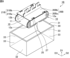
- FIG. 1 is a schematic perspective view showing an example of a capacitor according to a first embodiment of the present invention.
- FIG. 2 is a schematic perspective view showing an example of the capacitor shown in FIG. 1 (excluding the filled resin) in an exploded state.
- FIG. 3 is a schematic perspective view showing an example of the capacitor element shown in FIGS.
- FIG. 4 is a schematic cross-sectional view showing an example of a cross section of the capacitor element shown in FIG. 3 taken along line a1-a2.
- FIG. 5 is a schematic perspective view showing a state before the first lead terminal and the second lead terminal shown in FIG. 2 are locked.
- FIG. 6 is a schematic perspective view showing a state after the first lead terminal and the second lead terminal shown in FIG. 5 have been locked.
- FIG. 5 is a schematic perspective view showing a state before the first lead terminal and the second lead terminal shown in FIG. 2 are locked.
- FIG. 7 is a schematic perspective view showing an example of a capacitor according to the second embodiment of the present invention.
- FIG. 8 is a schematic perspective view showing an example of the capacitor shown in FIG. 7 (excluding the filled resin) in an exploded state.
- FIG. 9 is a schematic perspective view showing a state before the first lead terminal and the second lead terminal shown in FIG. 8 are locked.
- FIG. 10 is a schematic perspective view showing a state in which the first lead terminal and the second lead terminal shown in FIG. 9 are being locked.
- FIG. 11 is a schematic perspective view showing a state after the first lead terminal and the second lead terminal shown in FIG. 10 have been locked.
- a film capacitor is shown as an example of a capacitor of the present invention.
- the capacitor of the present invention can also be applied to capacitors other than film capacitors.
- the capacitor of the present invention comprises a capacitor element having a body and an external electrode provided on an end face of the body, a pull-out terminal electrically connected to the external electrode, an exterior case in which the capacitor element is housed so that the pull-out terminal protrudes outward, and a filling resin filled inside the exterior case so as to embed the capacitor element, the pull-out terminal having a first pull-out terminal and a second pull-out terminal electrically connected to the external electrode via the first pull-out terminal, and the first pull-out terminal and the second pull-out terminal are engaged so as to make surface contact.
- one of the first and second pull-out terminals has a first claw-shaped portion and a second claw-shaped portion located at a different height than the first claw-shaped portion in the first direction, and the other of the first and second pull-out terminals is sandwiched between the first and second claw-shaped portion in the first direction.
- FIG. 1 is a schematic perspective view showing an example of a capacitor according to a first embodiment of the present invention.
- FIG. 2 is a schematic perspective view showing an example of the capacitor shown in FIG. 1 (excluding the filled resin) in a disassembled state.
- the capacitor 1A shown in Figures 1 and 2 has a capacitor element 10 (see Figure 3 described later), a pull-out terminal 20A, a pull-out terminal 21A, an exterior case 30, and a filling resin 40.
- the first direction D1, the second direction D2, and the third direction D3 are perpendicular to each other.
- FIG. 3 is a schematic perspective view showing an example of the capacitor element shown in FIGS. 1 and 2.
- FIG. 4 is a schematic cross-sectional view showing an example of a cross-section along line a1-a2 of the capacitor element shown in FIG. 3.
- the capacitor element 10 shown in Figures 3 and 4 has a body 11, a first external electrode 12a, and a second external electrode 12b.
- the element body 11 is a wound body in which the first metallized film 13a and the second metallized film 13b are wound in a stacked state in the first direction D1.
- the capacitor 1A or more specifically, the capacitor element 10 is a wound-type film capacitor in which the metallized films are stacked and wound.
- capacitor 1A or more specifically, capacitor element 10
- capacitor element 10 may be a laminated film capacitor in which metallized films are laminated.
- element body 11 has a flat cross-sectional shape when viewed in a cross section perpendicular to the winding axis direction of element body 11 (third direction D3 in FIG. 3). More specifically, it is preferable that element body 11 has a cross-sectional shape pressed into a flat shape such as an ellipse or oval, and that the cross-sectional shape of element body 11 is thinner than when it is a perfect circle.
- Whether the base body has been pressed to have a flat cross-sectional shape can be confirmed, for example, by checking whether or not there are press marks on the base body.
- the capacitor element 10 may have a cylindrical winding axis.
- the winding axis is disposed on the central axis of the first metallized film 13a and the second metallized film 13b in the wound state, and serves as the winding axis when winding the first metallized film 13a and the second metallized film 13b.
- the first metallized film 13a has a first dielectric film 14a and a first metal layer 15a.
- the first dielectric film 14a has a first principal surface 14aa and a second principal surface 14ab that face each other in the first direction D1.
- the first metal layer 15a is provided on the first main surface 14aa of the first dielectric film 14a. More specifically, the first metal layer 15a is provided on the first main surface 14aa of the first dielectric film 14a so as to reach one side edge of the first dielectric film 14a in the third direction D3, but not to reach the other side edge of the first dielectric film 14a.
- the second metallized film 13b has a second dielectric film 14b and a second metal layer 15b.
- the second dielectric film 14b has a first main surface 14ba and a second main surface 14bb that face each other in the first direction D1.
- the second metal layer 15b is provided on the first main surface 14ba of the second dielectric film 14b. More specifically, the second metal layer 15b is provided on the first main surface 14ba of the second dielectric film 14b so as not to reach one side edge of the second dielectric film 14b in the third direction D3, but to reach the other side edge of the second dielectric film 14b.
- the adjacent first metallized films 13a and second metallized films 13b are shifted in the third direction D3 so that the end of the first metal layer 15a that reaches the side edge of the first dielectric film 14a is exposed on one end surface of the element body 11, and the end of the second metal layer 15b that reaches the side edge of the second dielectric film 14b is exposed on the other end surface of the element body 11.
- the first metallized film 13a protrudes toward the first external electrode 12a relative to the second metallized film 13b.
- the second metallized film 13b protrudes toward the second external electrode 12b relative to the first metallized film 13a.
- the first metal layer 15a is connected to the first external electrode 12a and is not connected to the second external electrode 12b.
- the second metal layer 15b is connected to the second external electrode 12b and is not connected to the first external electrode 12a.
- the adjacent first metallized film 13a and second metallized film 13b are shifted in the third direction D3 as described above, so that in the adjacent first dielectric film 14a and second dielectric film 14b, the first dielectric film 14a having the first metal layer 15a on the first main surface 14aa protrudes toward the first external electrode 12a relative to the second dielectric film 14b having the first metal layer 15a not provided on its main surface.
- the second dielectric film 14b having the second metal layer 15b on the first main surface 14ba protrudes toward the second external electrode 12b relative to the first dielectric film 14a having the second metal layer 15b not provided on its main surface.
- the element body 11 is formed by winding the first metallized film 13a and the second metallized film 13b in a stacked state in the first direction D1, and therefore can be said to include the first dielectric film 14a, the first metal layer 15a, the second dielectric film 14b, and the second metal layer 15b in the first direction D1. It can also be said that the element body 11 is a wound body formed by winding the first dielectric film 14a, the first metal layer 15a, the second dielectric film 14b, and the second metal layer 15b in the first direction D1.
- the first main surface 14aa of the first dielectric film 14a and the second main surface 14bb of the second dielectric film 14b face each other in the first direction D1
- the second main surface 14ab of the first dielectric film 14a and the first main surface 14ba of the second dielectric film 14b face each other in the first direction D1.
- the first metallized film 13a and the second metallized film 13b are wound in a state in which they are stacked in the first direction D1.
- the first metallized film 13a and the second metallized film 13b are wound in a state in which they are stacked in the first direction D1, so that the second metallized film 13b is on the inside of the first metallized film 13a, and more specifically, the first metal layer 15a is on the inside of the first dielectric film 14a, and the second metal layer 15b is on the inside of the second dielectric film 14b. That is, in the element body 11, the first metal layer 15a and the second metal layer 15b face each other with the first dielectric film 14a or the second dielectric film 14b sandwiched between them.
- the first metal layer 15a may be provided with a fuse portion.
- the fuse portion provided in the first metal layer 15a is, for example, a portion of the first metal layer 15a that connects a divided electrode portion in which the portion facing the second metal layer 15b is divided into multiple portions, and an electrode portion that does not face the second metal layer 15b.
- Examples of electrode patterns of the first metal layer 15a provided with a fuse portion include the electrode patterns disclosed in JP 2004-363431 A and JP 5-251266 A.
- the second metal layer 15b may also be provided with a fuse portion, similar to the first metal layer 15a.
- the first dielectric film 14a may contain a curable resin as a main component.
- the main component means the component with the highest weight percentage, preferably the component with a weight percentage greater than 50% by weight.
- the curable resin may be a thermosetting resin or a photocurable resin.
- thermosetting resin means a resin that can be cured by heat, but the curing method is not limited. Therefore, thermosetting resin also includes resins that can be cured by methods other than heat (for example, light, electron beam, etc.) so long as they are heat-curable. Also, depending on the material, a reaction may be initiated due to the reactivity of the material itself, and resins that proceed to cure without necessarily being subjected to heat from the outside are also considered to be thermosetting resins. The same applies to photocurable resins, and so long as they are light-curable, they also include resins that can be cured by methods other than light (for example, heat, etc.).
- the curable resin is preferably made of a cured product of a first organic material having a hydroxyl group (OH group) and a second organic material having an isocyanate group (NCO group).
- the curable resin is made of a cured product having a urethane bond obtained by reacting the hydroxyl group of the first organic material with the isocyanate group of the second organic material.
- FT-IR Fourier transform infrared spectrophotometer
- the first dielectric film 14a may contain at least one of a hydroxyl group and an isocyanate group.
- the first dielectric film 14a may contain either a hydroxyl group or an isocyanate group, or may contain both a hydroxyl group and an isocyanate group.
- Examples of the first organic material include phenoxy resin, polyvinyl acetoacetal resin, polyvinyl butyral resin, etc.
- the second organic material examples include aromatic polyisocyanates such as diphenylmethane diisocyanate (MDI) and tolylene diisocyanate (TDI), and aliphatic polyisocyanates such as hexamethylene diisocyanate (HDI).
- aromatic polyisocyanates such as diphenylmethane diisocyanate (MDI) and tolylene diisocyanate (TDI)
- aliphatic polyisocyanates such as hexamethylene diisocyanate (HDI).
- HDI hexamethylene diisocyanate
- the second organic material multiple types of organic materials may be used in combination.
- the first dielectric film 14a may contain a thermoplastic resin as a main component.
- thermoplastic resins examples include polypropylene, polyethersulfone, polyetherimide, polyarylate, etc.
- the first dielectric film 14a may contain additives to impart various functions.
- Additives include, for example, leveling agents to impart smoothness.
- the additive preferably has a functional group that reacts with a hydroxyl group and/or an isocyanate group and forms part of the crosslinked structure of the cured product.
- examples of such additives include resins having at least one functional group selected from the group consisting of a hydroxyl group, an epoxy group, a silanol group, and a carboxyl group.
- the second dielectric film 14b may contain a thermosetting resin as a main component, a photocurable resin as a main component, or a thermoplastic resin as a main component.
- the second dielectric film 14b may also contain an additive, like the first dielectric film 14a.
- compositions of the first dielectric film 14a and the second dielectric film 14b may be different from each other, but are preferably the same.
- the thickness of the first dielectric film 14a and the second dielectric film 14b is preferably 1 ⁇ m or more and 10 ⁇ m or less, and more preferably 3 ⁇ m or more and 5 ⁇ m or less.
- the thicknesses of the first dielectric film 14a and the second dielectric film 14b may be different from each other, but it is preferable that they are the same.
- the thickness of the dielectric film is measured using an optical thickness gauge.
- the first dielectric film 14a and the second dielectric film 14b are each preferably produced by forming a resin solution containing the resin material as described above into a film and then curing it by heat treatment.
- Examples of materials that can be used to form the first metal layer 15a and the second metal layer 15b include metals such as aluminum, zinc, titanium, magnesium, tin, and nickel.
- compositions of the first metal layer 15a and the second metal layer 15b may be different from each other, but are preferably the same.
- the thickness of the first metal layer 15a and the second metal layer 15b is preferably 5 nm or more and 40 nm or less.
- the thicknesses of the first metal layer 15a and the second metal layer 15b may be different from each other, but are preferably the same.
- the thickness of the metal layer is measured by observing a cross section of the metallized film along the first direction using a transmission electron microscope (TEM).
- TEM transmission electron microscope
- the first metal layer 15a and the second metal layer 15b are preferably formed by depositing a metal such as that described above onto the main surfaces of the first dielectric film 14a and the second dielectric film 14b, respectively.
- the first external electrode 12a is provided on one end surface of the element body 11. More specifically, the first external electrode 12a is connected to the first metal layer 15a by contacting the end of the first metal layer 15a exposed on one end surface of the element body 11. On the other hand, the first external electrode 12a is not connected to the second metal layer 15b.
- the second external electrode 12b is provided on the other end surface of the element body 11. More specifically, the second external electrode 12b is connected to the second metal layer 15b by contacting the end of the second metal layer 15b exposed on the other end surface of the element body 11. On the other hand, the second external electrode 12b is not connected to the first metal layer 15a.
- the constituent materials of the first external electrode 12a and the second external electrode 12b include metals such as zinc, aluminum, tin, and zinc-aluminum alloys.
- compositions of the first external electrode 12a and the second external electrode 12b may be different from each other, but are preferably the same.
- the first external electrode 12a and the second external electrode 12b are preferably formed by spraying a metal such as that described above onto one end face and the other end face of the body 11, respectively.
- the draw-out terminal 20A is electrically connected to the first external electrode 12a.
- the draw-out terminal 20A is electrically connected to the first external electrode 12a via a joining member such as solder.
- the pull-out terminal 20A has a first pull-out terminal 20Aa and a second pull-out terminal 20Ab.
- the first pull-out terminal 20Aa may be electrically located closest to the first external electrode 12a in the pull-out terminal 20A.
- the first pull-out terminal 20Aa may be located closest to the first external electrode 12a in the electrical path extending from the first external electrode 12a to the pull-out terminal 20A.
- the first pull-out terminal 20Aa does not have to be located electrically closest to the first external electrode 12a in the pull-out terminal 20A. In other words, the first pull-out terminal 20Aa does not have to be located closest to the first external electrode 12a in the electrical path between the first external electrode 12a and the pull-out terminal 20A. In other words, the pull-out terminal 20A may have another pull-out terminal that is electrically closer to the first external electrode 12a than the first pull-out terminal 20Aa.
- the second pull-out terminal 20Ab is electrically connected to the first external electrode 12a via the first pull-out terminal 20Aa.
- the second pull-out terminal 20Ab is provided at a position electrically farther away from the first external electrode 12a than the first pull-out terminal 20Aa.
- the second pull-out terminal 20Ab may be located on the side of the pull-out terminal 20A that is electrically opposite the first external electrode 12a.
- the second pull-out terminal 20Ab may be located on the side of the electrical path between the first external electrode 12a and the pull-out terminal 20A that is closest to the first external electrode 12a.
- the second pull-out terminal 20Ab does not have to be located on the most electrically opposite side of the pull-out terminal 20A from the first external electrode 12a.
- the second pull-out terminal 20Ab does not have to be located on the most opposite side of the first external electrode 12a in the electrical path between the first external electrode 12a and the pull-out terminal 20A.
- the pull-out terminal 20A may have another pull-out terminal that is provided at a position electrically farther away from the first external electrode 12a than the second pull-out terminal 20Ab.
- the first pull-out terminal 20Aa and the second pull-out terminal 20Ab are engaged so as to make surface contact.
- FIG. 5 is a schematic perspective view showing the state before the first and second pull-out terminals shown in FIG. 2 are locked.
- FIG. 6 is a schematic perspective view showing the state after the first and second pull-out terminals shown in FIG. 5 are locked. Note that in FIGS. 5 and 6, other components such as the capacitor element are omitted to make it easier to focus on the locking state of the first and second pull-out terminals.
- the first pull-out terminal 20Aa has a first claw portion 25a and a second claw portion 25b.
- the second claw portion 25b is located at a different height than the first claw portion 25a in the first direction D1.
- the second claw portion 25b may be located lower than the first claw portion 25a in the first direction D1, i.e., closer to the capacitor element 10 (see FIG. 2) than the first claw portion 25a in the first direction D1.
- the second claw portion 25b may be located higher than the first claw portion 25a in the first direction D1, i.e., farther from the capacitor element 10 (see FIG. 2) than the first claw portion 25a in the first direction D1.
- two claw-shaped portions located at different heights in the same direction means that at least the tips of the two claw-shaped portions are located at different heights in the same direction (first direction D1 in Figure 5).
- the first claw portion 25a and the second claw portion 25b do not have to overlap when viewed from the first direction D1.
- the first claw portion 25a and the second claw portion 25b may overlap when viewed from the first direction D1.
- the first pull-out terminal 20Aa may further include a third claw portion 25c.
- the third claw portion 25c may be located at the same height as the second claw portion 25b in the first direction D1. In other words, as shown in FIG. 5, the third claw portion 25c may be located at a different height than the first claw portion 25a in the first direction D1, similar to the second claw portion 25b.
- the third claw portion 25c may be located lower than the first claw portion 25a in the first direction D1, i.e., closer to the capacitor element 10 (see FIG. 2) than the first claw portion 25a in the first direction D1.
- the third claw portion 25c may be located at the same height as the first claw portion 25a or the same height as the second claw portion 25b in the first direction D1.
- two claw-shaped portions are located at the same height in the same direction (first direction D1 in Figure 5) means that at least the tips of the two claw-shaped portions are located at the same height in the same direction (first direction D1 in Figure 5).
- the first claw portion 25a and the third claw portion 25c do not have to overlap when viewed from the first direction D1.
- the first claw portion 25a and the third claw portion 25c may overlap when viewed from the first direction D1.
- the first claw portion 25a may be located between the second claw portion 25b and the third claw portion 25c in the second direction D2 perpendicular to the first direction D1 when viewed from the first direction D1.
- first claw portion 25a does not have to be located between the second claw portion 25b and the third claw portion 25c in the second direction D2 when viewed from the first direction D1.
- the second pull-out terminal 20Ab is sandwiched between the first claw portion 25a and the second claw portion 25b in the first direction D1. More specifically, the second pull-out terminal 20Ab is sandwiched by the elastic force of the first claw portion 25a and the second claw portion 25b in the first direction D1. Furthermore, as shown in FIG. 6, if the first pull-out terminal 20Aa further has a third claw portion 25c, the second pull-out terminal 20Ab is sandwiched between the first claw portion 25a and the third claw portion 25c in the first direction D1. More specifically, the second pull-out terminal 20Ab is sandwiched by the elastic force of the first claw portion 25a and the third claw portion 25c in the first direction D1.
- the first pull-out terminal 20Aa has the first claw portion 25a, the second claw portion 25b, and the third claw portion 25c, but instead of the first pull-out terminal 20Aa, the second pull-out terminal 20Ab may have the first claw portion 25a, the second claw portion 25b, and the third claw portion 25c. In this case, instead of the second pull-out terminal 20Ab, the first pull-out terminal 20Aa may be sandwiched between the first claw portion 25a and the second claw portion 25b and also between the first claw portion 25a and the third claw portion 25c in the first direction D1.
- the first pull-out terminal 20Aa has three claw-shaped portions, the first claw-shaped portion 25a, the second claw-shaped portion 25b, and the third claw-shaped portion 25c, but the number of claw-shaped portions is not particularly limited as long as it has at least two, the first claw-shaped portion 25a and the second claw-shaped portion 25b. The same applies when the second pull-out terminal 20Ab has claw-shaped portions.
- the first pull-out terminal 20Aa and the second pull-out terminal 20Ab are sandwiched between the multiple claw-shaped portions of one of the first pull-out terminal 20Aa and the second pull-out terminal 20Ab.
- the first pull-out terminal 20Aa and the second pull-out terminal 20Ab are engaged so as to be in surface contact.
- the first pull-out terminal 20Aa and the second pull-out terminal 20Ab are engaged, so that the first pull-out terminal 20Aa and the second pull-out terminal 20Ab can be mechanically (physically) connected without using a joining material such as solder. Therefore, in the capacitor 1A, the connectivity between the first pull-out terminal 20Aa and the second pull-out terminal 20Ab can be improved without using a joining material such as solder.
- connection points of the first and second pull-out terminals 20Aa and 20Ab can be held firmly without using a joining material such as solder, improving handling (assembly workability) when assembling the capacitor 1A, for example, when storing the capacitor element 10 connected to the pull-out terminal 20A in the exterior case 30.
- the first and second pull-out terminals 20Aa and 20Ab are in surface contact when connected as described above, so it is easy to weld the first and second pull-out terminals 20Aa and 20Ab. For this reason, it is preferable that the first and second pull-out terminals 20Aa and 20Ab are welded at points where they are engaged so as to be in surface contact.
- the second pull-out terminal 20Ab may be provided with a notch 26.
- the second pull-out terminal 20Ab has a notch 26, it is preferable that the first claw-shaped portion 25a is fitted into the notch 26. In this case, the first claw-shaped portion 25a is prevented from shifting in the second direction D2 by the notch 26, so that the first pull-out terminal 20Aa and the second pull-out terminal 20Ab are sufficiently firmly locked.
- the second pull-out terminal 20Ab has a notch 26, but if the second pull-out terminal 20Ab has a first claw-shaped portion 25a instead of the first pull-out terminal 20Aa, the first pull-out terminal 20Aa may have a notch 26 instead of the second pull-out terminal 20Ab, and the first claw-shaped portion 25a of the second pull-out terminal 20Ab may be fitted into the notch 26 provided in the first pull-out terminal 20Aa.
- the timing at which the first pull-out terminal 20Aa and the first external electrode 12a are connected as shown in Figure 2 may be before the first pull-out terminal 20Aa and the second pull-out terminal 20Ab are locked, or may be after the first pull-out terminal 20Aa and the second pull-out terminal 20Ab are locked.
- the draw-out terminal 21A is electrically connected to the second external electrode 12b.
- the draw-out terminal 21A is electrically connected to the second external electrode 12b via a joining member such as solder.
- the pull-out terminal 21A has a first pull-out terminal 21Aa and a second pull-out terminal 21Ab.
- the first pull-out terminal 21Aa may be electrically located closest to the second external electrode 12b in the pull-out terminal 21A.
- the first pull-out terminal 21Aa may be located closest to the second external electrode 12b in the electrical path extending from the second external electrode 12b to the pull-out terminal 21A.
- the first pull-out terminal 21Aa does not have to be electrically located closest to the second external electrode 12b in the pull-out terminal 21A. In other words, the first pull-out terminal 21Aa does not have to be located closest to the second external electrode 12b in the electrical path between the second external electrode 12b and the pull-out terminal 21A. In other words, the pull-out terminal 21A may have another pull-out terminal that is electrically closer to the second external electrode 12b than the first pull-out terminal 21Aa.
- the second pull-out terminal 21Ab is electrically connected to the second external electrode 12b via the first pull-out terminal 21Aa.
- the second pull-out terminal 21Ab is provided at a position electrically farther away from the second external electrode 12b than the first pull-out terminal 21Aa.
- the second pull-out terminal 21Ab may be located on the side of the pull-out terminal 21A that is electrically opposite the second external electrode 12b.
- the second pull-out terminal 21Ab may be located on the side of the electrical path between the second external electrode 12b and the pull-out terminal 21A that is closest to the second external electrode 12b.
- the second pull-out terminal 21Ab does not have to be located on the most electrically opposite side of the second external electrode 12b in the pull-out terminal 21A.
- the second pull-out terminal 21Ab does not have to be located on the most opposite side of the second external electrode 12b in the electrical path between the second external electrode 12b and the pull-out terminal 21A.
- the pull-out terminal 21A may have another pull-out terminal that is provided at a position electrically farther away from the second external electrode 12b than the second pull-out terminal 21Ab.
- first pull-out terminal 21Aa and the second pull-out terminal 21Ab are engaged so as to make surface contact.
- the first pull-out terminal 21Aa and the second pull-out terminal 21Ab when the first pull-out terminal 21Aa and the second pull-out terminal 21Ab are engaged, the first pull-out terminal 21Aa and the second pull-out terminal 21Ab can be mechanically (physically) connected without using a joining material such as solder.
- the connectivity between the first pull-out terminal 21Aa and the second pull-out terminal 21Ab can be improved without using a joining material such as solder.
- connection points of the first and second pull-out terminals 21Aa and 21Ab can be held firmly without using a joining material such as solder, improving handling (assembly workability) when assembling the capacitor 1A, for example, when storing the capacitor element 10 to which the pull-out terminals 21A are connected in the exterior case 30.
- first and second pull-out terminals 21Aa and 21Ab when welding the first and second pull-out terminals 21Aa and 21Ab to further strengthen the connection points of the first and second pull-out terminals 21Aa and 21Ab, if the first and second pull-out terminals 21Aa and 21Ab are in surface contact when connected as described above, it is easier to weld the first and second pull-out terminals 21Aa and 21Ab. For this reason, it is preferable that the first and second pull-out terminals 21Aa and 21Ab are welded at points where they are engaged so as to make surface contact.
- the capacitor 1A it is sufficient that at least the first pull-out terminal 20Aa and the second pull-out terminal 20Ab are engaged so as to make surface contact, and it is preferable that the first pull-out terminal 21Aa and the second pull-out terminal 21Ab are engaged so as to make surface contact, but they do not have to be engaged so as to make surface contact.
- the engaging manner of the first and second drawn-out terminals 21Aa and 21Ab is preferably the same as the engaging manner of the first and second drawn-out terminals 20Aa and 20Ab described above, but may be different from the engaging manner of the first and second drawn-out terminals 20Aa and 20Ab.
- the shape of the pull-out terminal 20A may be, for example, plate-like or linear (rod-like). That is, the shape of the first pull-out terminal 20Aa and the second pull-out terminal 20Ab may each be, for example, plate-like or linear (rod-like). In this case, the first pull-out terminal 20Aa and the second pull-out terminal 20Ab may each have a shape with a partially bent portion.
- the shape of the drawer terminal 21A may be, for example, plate-like or linear (rod-like). That is, the shape of the first drawer terminal 21Aa and the second drawer terminal 21Ab may each be, for example, plate-like or linear (rod-like). In this case, the first drawer terminal 21Aa and the second drawer terminal 21Ab may each have a shape with a partially bent portion.
- the first pull-out terminal 20Aa, the second pull-out terminal 20Ab, the first pull-out terminal 21Aa, and the second pull-out terminal 21Ab are each also called a bus bar.
- the pull-out terminal 20A and the pull-out terminal 21A are each used as terminals for electrically connecting the capacitor element 10 to an object to be mounted, for example, when mounting the capacitor 1A to the object to be mounted.
- the capacitor element 10 is housed inside the exterior case 30 so that the pull-out terminals 20A and 21A protrude toward the outside.
- the capacitor element 10 be stored in the center of the interior of the outer case 30, away from the inner surface of the outer case 30.
- one capacitor element 10 is stored inside one exterior case 30, but multiple capacitor elements 10 may be stored inside one exterior case 30.
- the shape of the exterior case 30 is, for example, a cylindrical shape with a bottom and an opening 31 at one end in the first direction D1, as shown in Figures 1 and 2.
- the outer surface of the exterior case 30 includes a first outer surface 32 facing the opening 31 in the first direction D1, and a second outer surface 33 (in the example shown in Figures 1 and 2, four outer surfaces are included) extending from the first outer surface 32 toward the opening 31 in the first direction D1.
- Examples of the exterior case 30 include a resin case, a metal case, etc.
- the exterior case 30 is a resin case
- the resin that constitutes the resin case include liquid crystal polymer (LCP), polyphenylene sulfide, polybutylene terephthalate, etc.
- LCP liquid crystal polymer
- the resin case contains a liquid crystal polymer.
- the liquid crystal polymer contained in the resin case may be, for example, a liquid crystal polymer having p-hydroxybenzoic acid and 6-hydroxy-2-naphthoic acid groups in its skeleton.
- liquid crystal polymers formed from polycondensates using various components such as phenol, phthalic acid, and ethylene terephthalate can also be used.
- Liquid crystal polymers can also be classified into types I, II, and III, but the material used is the same as the liquid crystal polymer formed from the above-mentioned components.
- the resin case preferably further contains an inorganic filler in addition to the liquid crystal polymer.
- the inorganic filler contained in the resin case can be a material that is stronger than the liquid crystal polymer.
- the inorganic filler is preferably a material that has a higher melting point than the liquid crystal polymer, and more preferably a material with a melting point of 680°C or higher.
- the shape of the inorganic filler is not particularly limited, and examples include a shape having a longitudinal direction such as a fiber shape or a plate shape.
- As an inorganic filler of such a shape multiple types of inorganic materials may be used in combination.
- the resin case contains at least one of a fibrous inorganic material and a plate-shaped inorganic material as the inorganic filler.
- a filler being fibrous means that the relationship between the longitudinal dimension in the longitudinal direction and the cross-sectional diameter in a cross section perpendicular to the longitudinal direction is longitudinal dimension/cross-sectional diameter ⁇ 5 (i.e., the aspect ratio is 5:1 or more).
- the cross-sectional diameter is the longest distance between two points on the circumference of the cross section. If the cross-sectional diameter varies in the longitudinal direction, the measurement is taken at the point where the cross-sectional diameter is largest.
- a filler being plate-like means that the relationship between the cross-sectional diameter of the face with the largest projected area and the maximum height in the direction perpendicular to this cross section is cross-sectional diameter/maximum height ⁇ 3.
- the inorganic filler has a portion oriented from the first outer surface 32 toward the opening 31 on the second outer surface 33 of the exterior case 30 and a portion oriented toward the adjacent second outer surface 33, and is dispersed inside the exterior case 30.
- the size of the inorganic filler is preferably 5 ⁇ m or more in diameter and 50 ⁇ m or more in length.
- the inorganic filler be dispersed throughout the exterior case 30 without agglomerating.
- inorganic fillers examples include inorganic materials such as fibrous glass filler, plate-like talc or mica. Of these, it is preferable for the inorganic filler to contain fibrous glass filler as the main component.
- the resin case contains another resin (e.g., polyphenylene sulfide) instead of the liquid crystal polymer, it is preferable that the resin case further contains an inorganic filler as described above.
- another resin e.g., polyphenylene sulfide
- the resin case is manufactured by a method such as injection molding.
- the exterior case 30 is a metal case
- the metal that constitutes the metal case include simple metals such as aluminum, magnesium, iron, stainless steel, and copper, and alloys that contain at least one of these simple metals. Of these, it is preferable that the metal case contains aluminum or an aluminum alloy.
- the metal case is manufactured by a method such as impact molding.
- the filled resin 40 is filled inside the exterior case 30 so as to embed the capacitor element 10.
- the capacitor element 10 is held inside the exterior case 30.
- the filling resin 40 is filled between the capacitor element 10 and the exterior case 30, more specifically, between the outer surface of the capacitor element 10 and the inner surface of the exterior case 30. Furthermore, inside the exterior case 30, the filling resin 40 is filled not only between the capacitor element 10 and the exterior case 30, but also in the area from the opening 31 of the exterior case 30 to the capacitor element 10.
- the filling resin 40 it is preferable to appropriately select a resin with low moisture permeability from the viewpoint of suppressing the infiltration of moisture into the capacitor element 10, and examples thereof include epoxy resin, silicone resin, urethane resin, etc.
- examples of the hardener for the epoxy resin include an amine hardener, an imidazole hardener, etc.
- the filling resin 40 only the above-mentioned resin may be used, but in order to improve strength, a resin to which a reinforcing agent has been added may also be used.
- reinforcing agents include silica and alumina.
- the thickness of the filling resin 40 at the opening 31 of the exterior case 30 is large.
- the thickness of the filling resin 40 at the opening 31 of the exterior case 30 is preferably sufficiently large within the range that allows for the volume (physical size) of the entire capacitor 1A, and specifically, is preferably 2 mm or more, and more preferably 4 mm or more.
- the thickness of the filling resin 40 for the capacitor element 10 is made larger on the opening 31 side of the exterior case 30 than on the first outer surface 32 side by arranging the capacitor element 10 on the opening 31 side of the exterior case 30 inside the exterior case 30.
- the thickness of the filling resin 40 is measured, for example, using a soft X-ray device if it is in a non-destructive state, and using a length measuring device such as a caliper if it is in a destructive state.
- the relationship between the height of the outer case 30 and the height of the filled resin 40 in the first direction D1 is such that the thickness of the filled resin 40 at the opening 31 of the outer case 30 is as large as possible, and may be up to a position on the inside of the outer case 30, may be nearly to the top, or may overflow slightly due to surface tension.
- the pull-out terminal 20A in the pull-out terminal 20A, at least a portion of the first pull-out terminal 20Aa (see FIG. 2) may be embedded in the filling resin 40. In the example shown in FIG. 1, the entire first pull-out terminal 20Aa is embedded in the filling resin 40.
- the pull-out terminal 21A in the pull-out terminal 21A, at least a portion of the first pull-out terminal 21Aa (see FIG. 2) may be embedded in the filling resin 40. In the example shown in FIG. 1, the entire first pull-out terminal 21Aa is embedded in the filling resin 40.
- the second pull-out terminal 20Ab may protrude from the filling resin 40.
- a portion (end) of the second pull-out terminal 20Ab protrudes from the filling resin 40.
- the second pull-out terminal 21Ab may protrude from the filling resin 40.
- a portion (end) of the second pull-out terminal 21Ab protrudes from the filling resin 40.
- one of the first and second lead-out terminals has a claw-shaped portion
- the other of the first and second lead-out terminals has a slit portion penetrating in a first direction
- the claw-shaped portion is inserted through the slit portion in the first direction and hooked onto an edge of the slit portion.
- the capacitor of the second embodiment of the present invention is otherwise similar to the capacitor of the first embodiment of the present invention.
- FIG. 7 is a schematic perspective view showing an example of a capacitor according to embodiment 2 of the present invention.
- FIG. 8 is a schematic perspective view showing an example of the capacitor shown in FIG. 7 (excluding the filled resin) in a disassembled state.
- the capacitor 1B shown in Figures 7 and 8 has two capacitor elements 10 (see Figure 3 above), a pull-out terminal 20B, a pull-out terminal 21B, an exterior case 30, and a filling resin 40.
- two capacitor elements 10 are housed inside one exterior case 30, but one capacitor element 10 may be housed inside one exterior case 30, or three or more capacitor elements 10 may be housed inside one exterior case 30.
- the pull-out terminal 20B is electrically connected to each of the first external electrodes 12a of the two capacitor elements 10.
- the pull-out terminal 20B is electrically connected to each of the first external electrodes 12a of the two capacitor elements 10 via a joining member such as solder.
- the pull-out terminal 20B has a first pull-out terminal 20Ba and a second pull-out terminal 20Bb.
- the first pull-out terminal 20Ba and the second pull-out terminal 20Bb are engaged so as to make surface contact.
- the following describes the locking manner of the first pull-out terminal 20Ba and the second pull-out terminal 20Bb.
- FIG. 9 is a schematic perspective view showing the state before the first and second pull-out terminals shown in FIG. 8 are engaged.
- FIG. 10 is a schematic perspective view showing the state in which the first and second pull-out terminals shown in FIG. 9 are in the process of being engaged.
- FIG. 11 is a schematic perspective view showing the state after the first and second pull-out terminals shown in FIG. 10 have been engaged. Note that in FIGS. 9, 10, and 11, other components such as a capacitor element are omitted to make it easier to focus on the manner in which the first and second pull-out terminals are engaged.
- the first pull-out terminal 20Ba has a claw-shaped portion 25.
- the second pull-out terminal 20Bb has a slit portion 27.
- the slit portion 27 penetrates the second pull-out terminal 20Bb in the first direction D1.
- the slit portion 27 may include a first slit portion 27a and a second slit portion 27b.
- the second slit portion 27b is connected to the first slit portion 27a in a second direction D2 that is perpendicular to the first direction D1.
- the first slit portion 27a is capable of containing the claw-shaped portion 25.
- the slit portion when the slit portion is capable of containing the claw-shaped portion when viewed from the same direction (first direction D1 in FIG. 9), this means that when the claw-shaped portion and the slit portion are overlapped while viewed from the same direction (first direction D1 in FIG. 9), the claw-shaped portion does not protrude from the slit portion, or more specifically, the outer edge of the claw-shaped portion is not positioned outside the outer edge of the slit portion.
- the second slit portion 27b cannot contain the claw-shaped portion 25.
- the slit portion being unable to contain the claw portion when viewed from the same direction means that when the claw portion and the slit portion are overlapped while viewed from the same direction (first direction D1 in FIG. 9), the claw portion protrudes from the slit portion, or more specifically, the outer edge of the claw portion is positioned outside the outer edge of the slit portion.
- first slit portion 27a can contain the claw-shaped portion 25 when viewed from the first direction D1, the claw-shaped portion 25 can be directly inserted into the first slit portion 27a in the first direction D1, as shown in FIG. 10.
- the claw-shaped portion 25 cannot be directly inserted into the second slit portion 27b in the first direction D1.
- the claw-shaped portion 25 is capable of sliding in the second direction D2 between the first slit portion 27a and the second slit portion 27b when inserted into the slit portion 27 in the first direction D1.
- the dimension in the third direction D3 of the base side portion (portion extending in the first direction D1) located on the opposite side to the tip of the claw-shaped portion 25 is equal to or smaller than the dimension in the third direction D3 of the second slit portion 27b
- the claw-shaped portion 25 can slide in the second direction D2 between the first slit portion 27a and the second slit portion 27b when inserted into the first slit portion 27a in the first direction D1.
- the claw-shaped portion 25 When the claw-shaped portion 25 is slid in the second direction D2 toward the second slit portion 27b from the state shown in FIG. 10 in which the claw-shaped portion 25 is inserted into the first slit portion 27a in the first direction D1, as shown in FIG. 11, the claw-shaped portion 25 is hooked onto the edge of the slit portion 27 while being inserted into the slit portion 27 in the first direction D1. More specifically, as shown in FIG. 11, it is preferable that the claw-shaped portion 25 is hooked onto the edge of the second slit portion 27b. In this case, the claw-shaped portion 25 is positioned in the third direction D3 by the second slit portion 27b.
- the first pull-out terminal 20Ba has a claw-shaped portion 25, but instead of the first pull-out terminal 20Ba, the second pull-out terminal 20Bb may have the claw-shaped portion 25.
- the first pull-out terminal 20Ba may have a slit portion 27, and the claw-shaped portion 25 of the second pull-out terminal 20Bb may be inserted into the slit portion 27 provided in the first pull-out terminal 20Ba in the first direction D1 and hooked onto the edge of the slit portion 27.
- the claw-shaped portion 25 of one of the first and second pull-out terminals 20Ba and 20Bb is inserted in the first direction D1 through the slit portion 27 provided on the other of the first and second pull-out terminals 20Ba and 20Bb, and hooked onto the edge of the slit portion 27.
- the first and second pull-out terminals 20Ba and 20Bb are engaged so as to make surface contact.
- the first pull-out terminal 20Ba and the second pull-out terminal 20Bb are engaged, so that the first pull-out terminal 20Ba and the second pull-out terminal 20Bb can be mechanically (physically) connected without using a joining material such as solder. Therefore, in the capacitor 1B, the connectivity between the first pull-out terminal 20Ba and the second pull-out terminal 20Bb can be improved without using a joining material such as solder.
- connection points of the first pull-out terminal 20Ba and the second pull-out terminal 20Bb can be held firmly without using a joining material such as solder, improving handling (assembly workability) when assembling the capacitor 1B, for example, when storing the capacitor element 10 connected to the pull-out terminal 20B in the exterior case 30.
- the first and second pull-out terminals 20Ba and 20Bb are in surface contact when connected, and therefore it is easy to weld the first and second pull-out terminals 20Ba and 20Bb.
- the first and second pull-out terminals 20Ba and 20Bb are welded at points where they are engaged so as to make surface contact.
- the first pull-out terminal 20Ba and the second pull-out terminal 20Bb are engaged at two locations, but the number of locations at which the first pull-out terminal 20Ba and the second pull-out terminal 20Bb are engaged is not particularly limited.
- the first pull-out terminal 20Ba may further include a claw-shaped portion 25'.
- the claw-shaped portion 25' may be located at a different height than the claw-shaped portion 25 in the first direction D1.
- the claw-shaped portion 25' may be located lower than the claw-shaped portion 25 in the first direction D1, i.e., closer to the capacitor element 10 (see FIG. 8) than the claw-shaped portion 25 in the first direction D1.
- claw portion 25 and claw portion 25' do not have to overlap when viewed from the first direction D1.
- the second pull-out terminal 20Bb is sandwiched between the claw-shaped portions 25 and 25' in the first direction D1 as shown in FIG. 11.
- the second pull-out terminal 20Bb is less likely to shift in the first direction D1 when sandwiched between the claw-shaped portions 25 and 25', so that the first pull-out terminal 20Ba and the second pull-out terminal 20Bb are sufficiently firmly locked.
- the first pull-out terminal 20Ba has a claw-shaped portion 25 and a claw-shaped portion 25', but if the second pull-out terminal 20Bb has a claw-shaped portion 25 instead of the first pull-out terminal 20Ba, the second pull-out terminal 20Bb may further have a claw-shaped portion 25', and instead of the second pull-out terminal 20Bb, the first pull-out terminal 20Ba may be sandwiched between the claw-shaped portion 25 and the claw-shaped portion 25' of the second pull-out terminal 20Bb in the first direction D1.
- the first slit portion 27a and the second slit portion 27b are connected in the second direction D2, but they may be connected in the third direction D3 instead of the second direction D2.
- the claw-shaped portion 25 may be slidable in the third direction D3 between the first slit portion 27a and the second slit portion 27b while being inserted into the slit portion 27 in the first direction D1.
- the timing at which the first pull-out terminal 20Ba and the first external electrode 12a are connected as shown in Figure 8 may be before the first pull-out terminal 20Ba and the second pull-out terminal 20Bb are locked, or may be after the first pull-out terminal 20Ba and the second pull-out terminal 20Bb are locked.
- the pull-out terminal 21B is electrically connected to each of the second external electrodes 12b of the two capacitor elements 10.
- the pull-out terminal 21B is electrically connected to each of the second external electrodes 12b of the two capacitor elements 10 via a joining member such as solder.
- the lead-out terminal 20B is electrically connected to each of the first external electrodes 12a of the two capacitor elements 10 and the lead-out terminal 21B is electrically connected to each of the second external electrodes 12b of the two capacitor elements 10, the two capacitor elements 10 are connected in parallel.
- the pull-out terminal 21B has a first pull-out terminal 21Ba and a second pull-out terminal 21Bb.
- first pull-out terminal 21Ba and the second pull-out terminal 21Bb are engaged so as to make surface contact.
- the first pull-out terminal 21Ba and the second pull-out terminal 21Bb when the first pull-out terminal 21Ba and the second pull-out terminal 21Bb are engaged, the first pull-out terminal 21Ba and the second pull-out terminal 21Bb can be mechanically (physically) connected without using a joining material such as solder.
- the connectivity between the first pull-out terminal 21Ba and the second pull-out terminal 21Bb can be improved without using a joining material such as solder.
- connection points of the first pull-out terminal 21Ba and the second pull-out terminal 21Bb can be held firmly without using a joining material such as solder, improving handling (assembly workability) when assembling the capacitor 1B, for example, when storing the capacitor element 10 to which the pull-out terminal 21B is connected in the exterior case 30.
- first and second pull-out terminals 21Ba and 21Bb when welding the first and second pull-out terminals 21Ba and 21Bb to strengthen the connection points of the first and second pull-out terminals 21Ba and 21Bb, if the first and second pull-out terminals 21Ba and 21Bb are in surface contact when connected as described above, it is easier to weld the first and second pull-out terminals 21Ba and 21Bb. For this reason, it is preferable that the first and second pull-out terminals 21Ba and 21Bb are welded at points where they are engaged so as to make surface contact.
- the capacitor 1B it is sufficient that at least the first pull-out terminal 20Ba and the second pull-out terminal 20Bb are engaged so as to make surface contact, and it is preferable that the first pull-out terminal 21Ba and the second pull-out terminal 21Bb are engaged so as to make surface contact, but they do not have to be engaged so as to make surface contact.
- the engaging manner of the first and second drawn-out terminals 21Ba and 21Bb is preferably the same as the engaging manner of the first and second drawn-out terminals 20Ba and 20Bb described above, but may be different from the engaging manner of the first and second drawn-out terminals 20Ba and 20Bb.
- the engaging manner of the first and second drawn-out terminals 21Ba and 21Bb may be the same as the engaging manner of the first and second drawn-out terminals 20Aa and 20Ab described above.
- the capacitor of the present invention is useful, for example, as a smoothing capacitor that constitutes a power conversion device (e.g., an inverter) for in-vehicle use.
- a power conversion device e.g., an inverter
- a capacitor element having an element body and external electrodes provided on end faces of the element body; A lead terminal electrically connected to the external electrode; an exterior case in which the capacitor element is housed so that the lead-out terminal protrudes outward; a filling resin filled inside the exterior case so as to embed the capacitor element, the lead-out terminal includes a first lead-out terminal and a second lead-out terminal electrically connected to the external electrode via the first lead-out terminal,
- the capacitor is characterized in that the first lead-out terminal and the second lead-out terminal are engaged so as to be in surface contact with each other.
- one of the first and second lead-out terminals has a first claw-shaped portion and a second claw-shaped portion located at a different height from the first claw-shaped portion in a first direction;
- one of the first and second lead terminals further includes a third claw portion located at the same height as the second claw portion in the first direction;
- a notch portion is provided in the other of the first lead terminal and the second lead terminal,
- one of the first lead terminal and the second lead terminal has a claw-shaped portion, the other of the first and second drawn-out terminals is provided with a slit portion penetrating in a first direction,
- the capacitor according to any one of ⁇ 1> to ⁇ 8>, wherein the claw-shaped portion is inserted into the slit portion in the first direction and hooked onto an edge of the slit portion.
- the slit portion includes a first slit portion and a second slit portion connected to the first slit portion in a second direction perpendicular to the first direction,
- the capacitor described in ⁇ 9> wherein, when viewed from the first direction, the first slit portion is capable of containing the claw-shaped portion, and the second slit portion is not capable of containing the claw-shaped portion.
- Reference Signs List 1A, 1B Capacitor 10 Capacitor element 11 Body 12a First external electrode 12b Second external electrode 13a First metallized film 13b Second metallized film 14a First dielectric film 14aa First main surface 14ab of first dielectric film Second main surface 14b of first dielectric film Second dielectric film 14ba First main surface 14bb of second dielectric film Second main surface 15a of second dielectric film First metal layer 15b Second metal layer 20A, 20B, 21A, 21B Lead terminals 20Aa, 20Ba, 21Aa, 21Ba First lead terminals 20Ab, 20Bb, 21Ab, 21Bb Second lead terminals 25, 25' Claw-shaped portion 25a First claw-shaped portion 25b Second claw-shaped portion 25c Third claw-shaped portion 26 Notch portion 27 Slit portion 27a First slit portion 27b Second slit portion 30 Exterior case 31 Opening 32 First outer surface 33 Second outer surface 40 Filling resin D1 First direction D2 Second direction D3 Third direction
Landscapes
- Engineering & Computer Science (AREA)
- Power Engineering (AREA)
- Microelectronics & Electronic Packaging (AREA)
- Manufacturing & Machinery (AREA)
- Fixed Capacitors And Capacitor Manufacturing Machines (AREA)
Abstract
Description
本発明は、コンデンサに関する。 The present invention relates to a capacitor.
特許文献1には、端面に電極部(10a)を有するコンデンサ素子(10)をバスバー(20)で接続しケース(50)に収納するとともに樹脂(60)を充填し外部接続用端子(32)(42)をケース開口部(53)と略直交する方向に向かって引き出したコンデンサであって、該コンデンサは、さらに、端子台(70)を備えており、端子台(70)は、ケース(50)と接することなく、一方側が樹脂(60)に埋設されているとともに、他方側に設けられたネジ部(73a)が外部接続用端子(32)(42)の取付孔(32b)(42b)と対向していることを特徴とするコンデンサが開示されている。 Patent Document 1 discloses a capacitor in which a capacitor element (10) having electrodes (10a) on its end faces is connected by a bus bar (20) and housed in a case (50), which is filled with resin (60) and has external connection terminals (32) (42) drawn out in a direction approximately perpendicular to the case opening (53), and further includes a terminal block (70), one side of which is embedded in the resin (60) without contacting the case (50), and a screw portion (73a) provided on the other side faces the mounting holes (32b) (42b) of the external connection terminals (32) (42).
特許文献1に記載のコンデンサでは、コンデンサ素子の電極部に接続されたCP線とバスバーとがはんだによって接続される、とされている。しかしながら、特許文献1に記載のコンデンサでは、CP線とバスバーとをはんだによって接続しようとしても、はんだ接続時の熱がバスバーを介して外部に逃げやすくなるため、はんだの温度が下がりやすくなる。よって、特許文献1に記載のコンデンサでは、CP線とバスバーとをはんだによって接続することが困難である。 In the capacitor described in Patent Document 1, the CP wire connected to the electrode portion of the capacitor element and the bus bar are connected by soldering. However, in the capacitor described in Patent Document 1, even if you try to connect the CP wire and the bus bar by soldering, the heat generated during the soldering connection tends to escape to the outside through the bus bar, so the temperature of the solder is likely to drop. Therefore, in the capacitor described in Patent Document 1, it is difficult to connect the CP wire and the bus bar by soldering.
これに対して、特許文献1に記載のコンデンサにおいて、CP線とバスバーとを、はんだ接続ではなく溶接することが考えられる。しかしながら、特許文献1に記載のコンデンサにおいて、CP線とバスバーとを溶接しようとしても、特許文献1の図1等に記載の構造、コンデンサ素子のサイズのばらつき等によって、CP線とバスバーとを充分に面接触させることができない。よって、特許文献1に記載のコンデンサでは、CP線とバスバーとを溶接することが困難である。 In response to this, in the capacitor described in Patent Document 1, it is possible to weld the CP wire and the bus bar together rather than soldering them together. However, even if one attempts to weld the CP wire and the bus bar together in the capacitor described in Patent Document 1, the structure described in Figure 1 of Patent Document 1, variations in the size of the capacitor elements, and other factors make it impossible to achieve sufficient surface contact between the CP wire and the bus bar. Therefore, in the capacitor described in Patent Document 1, it is difficult to weld the CP wire and the bus bar together.
以上のように、従来のコンデンサでは、コンデンサ素子の電極部を外部に引き出すために複数の引出端子(特許文献1に記載のコンデンサでは、CP線及びバスバー)が接続された構造を用いる場合、はんだ等の接合部材を用いずに引出端子間(特許文献1に記載のコンデンサでは、CP線とバスバーとの間)の接続性を向上する点で改善の余地がある。 As described above, in conventional capacitors, when a structure is used in which multiple lead-out terminals (CP wires and bus bars in the capacitor described in Patent Document 1) are connected to lead out the electrodes of the capacitor element, there is room for improvement in terms of improving the connectivity between the lead-out terminals (between the CP wires and bus bars in the capacitor described in Patent Document 1) without using a joining material such as solder.
本発明は、上記の問題を解決するためになされたものであり、はんだ等の接合部材を用いずに引出端子間の接続性を向上可能なコンデンサを提供することを目的とするものである。 The present invention was made to solve the above problems, and aims to provide a capacitor that can improve the connectivity between the lead-out terminals without using joining materials such as solder.
本発明のコンデンサは、素体と、上記素体の端面上に設けられた外部電極と、を有するコンデンサ素子と、上記外部電極に電気的に接続された引出端子と、上記引出端子が外部に向かって突出するように上記コンデンサ素子が内部に収納された外装ケースと、上記コンデンサ素子を埋設させるように上記外装ケースの内部に充填された充填樹脂と、を備え、上記引出端子は、第1引出端子と、上記第1引出端子を介して上記外部電極に電気的に接続された第2引出端子と、を有し、上記第1引出端子及び上記第2引出端子は、面接触するように係止されている、ことを特徴とする。 The capacitor of the present invention comprises a capacitor element having a body and an external electrode provided on an end face of the body, a pull-out terminal electrically connected to the external electrode, an exterior case in which the capacitor element is housed so that the pull-out terminal protrudes outward, and a filling resin filled inside the exterior case so as to embed the capacitor element, the pull-out terminal having a first pull-out terminal and a second pull-out terminal electrically connected to the external electrode via the first pull-out terminal, and the first pull-out terminal and the second pull-out terminal are engaged so as to make surface contact.
本発明によれば、はんだ等の接合部材を用いずに引出端子間の接続性を向上可能なコンデンサを提供できる。 The present invention provides a capacitor that can improve the connectivity between lead terminals without using joining materials such as solder.
以下、本発明のコンデンサについて説明する。なお、本発明は、以下の構成に限定されるものではなく、本発明の要旨を逸脱しない範囲において適宜変更されてもよい。また、以下において記載する個々の好ましい構成を複数組み合わせたものもまた本発明である。 The capacitor of the present invention will be described below. Note that the present invention is not limited to the configuration below, and may be modified as appropriate without departing from the spirit of the present invention. In addition, a combination of multiple individual preferred configurations described below also constitutes the present invention.
以下に示す各実施形態は例示であり、異なる実施形態で示す構成の部分的な置換又は組み合わせが可能であることは言うまでもない。実施形態2以降では、実施形態1と共通の事項についての記載は省略し、異なる点を主に説明する。特に、同様の構成による同様の作用効果については、実施形態毎に逐次言及しない。 The embodiments shown below are merely examples, and it goes without saying that partial substitution or combination of the configurations shown in different embodiments is possible. From embodiment 2 onwards, descriptions of matters common to embodiment 1 will be omitted, and differences will be mainly explained. In particular, similar effects resulting from similar configurations will not be mentioned one by one for each embodiment.
以下の説明において、各実施形態を特に区別しない場合、単に「本発明のコンデンサ」と言う。 In the following description, unless otherwise specified, each embodiment will simply be referred to as the "capacitor of the present invention."
以下では、本発明のコンデンサの一例として、フィルムコンデンサを示す。本発明のコンデンサは、フィルムコンデンサ以外のコンデンサにも適用可能である。 Below, a film capacitor is shown as an example of a capacitor of the present invention. The capacitor of the present invention can also be applied to capacitors other than film capacitors.
以下に示す図面は模式図であり、その寸法、縦横比の縮尺等は実際の製品と異なる場合がある。 The drawings shown below are schematic diagrams, and the dimensions, aspect ratio, and other scales may differ from those of the actual product.
本明細書中、要素間の関係性を示す用語(例えば、「平行」、「直交」等)及び要素の形状を示す用語は、文字通りの厳密な態様のみを意味するだけではなく、実質的に同等な範囲、例えば、数%程度の差異を含む範囲も意味する。 In this specification, terms indicating the relationship between elements (e.g., "parallel," "orthogonal," etc.) and terms indicating the shapes of elements do not only mean the literal, strict form, but also mean a range that is substantially equivalent, for example, a range that includes a difference of about a few percent.
本発明のコンデンサは、素体と、上記素体の端面上に設けられた外部電極と、を有するコンデンサ素子と、上記外部電極に電気的に接続された引出端子と、上記引出端子が外部に向かって突出するように上記コンデンサ素子が内部に収納された外装ケースと、上記コンデンサ素子を埋設させるように上記外装ケースの内部に充填された充填樹脂と、を備え、上記引出端子は、第1引出端子と、上記第1引出端子を介して上記外部電極に電気的に接続された第2引出端子と、を有し、上記第1引出端子及び上記第2引出端子は、面接触するように係止されている、ことを特徴とする。 The capacitor of the present invention comprises a capacitor element having a body and an external electrode provided on an end face of the body, a pull-out terminal electrically connected to the external electrode, an exterior case in which the capacitor element is housed so that the pull-out terminal protrudes outward, and a filling resin filled inside the exterior case so as to embed the capacitor element, the pull-out terminal having a first pull-out terminal and a second pull-out terminal electrically connected to the external electrode via the first pull-out terminal, and the first pull-out terminal and the second pull-out terminal are engaged so as to make surface contact.
[実施形態1]
本発明の実施形態1のコンデンサにおいて、第1引出端子及び第2引出端子の一方は、第1爪状部と、第1方向において第1爪状部と異なる高さに位置する第2爪状部と、を有し、第1引出端子及び第2引出端子の他方は、第1方向において第1爪状部及び第2爪状部に挟み込まれている。
[Embodiment 1]
In the capacitor of embodiment 1 of the present invention, one of the first and second pull-out terminals has a first claw-shaped portion and a second claw-shaped portion located at a different height than the first claw-shaped portion in the first direction, and the other of the first and second pull-out terminals is sandwiched between the first and second claw-shaped portion in the first direction.
図1は、本発明の実施形態1のコンデンサの一例を示す斜視模式図である。図2は、図1に示すコンデンサ(ただし、充填樹脂を除く)が分解された状態の一例を示す斜視模式図である。 FIG. 1 is a schematic perspective view showing an example of a capacitor according to a first embodiment of the present invention. FIG. 2 is a schematic perspective view showing an example of the capacitor shown in FIG. 1 (excluding the filled resin) in a disassembled state.
図1及び図2に示すコンデンサ1Aは、コンデンサ素子10(後述する図3参照)と、引出端子20Aと、引出端子21Aと、外装ケース30と、充填樹脂40と、を有している。
The
図1等において、第1方向D1と第2方向D2と第3方向D3とは、互いに直交している。 In FIG. 1 etc., the first direction D1, the second direction D2, and the third direction D3 are perpendicular to each other.
図3は、図1及び図2に示すコンデンサ素子の一例を示す斜視模式図である。図4は、図3に示すコンデンサ素子の線分a1-a2に沿う断面の一例を示す断面模式図である。 FIG. 3 is a schematic perspective view showing an example of the capacitor element shown in FIGS. 1 and 2. FIG. 4 is a schematic cross-sectional view showing an example of a cross-section along line a1-a2 of the capacitor element shown in FIG. 3.
図3及び図4に示すコンデンサ素子10は、素体11と、第1外部電極12aと、第2外部電極12bと、を有している。
The
素体11は、第1金属化フィルム13aと第2金属化フィルム13bとが第1方向D1に積層された状態で巻回されてなる巻回体である。つまり、コンデンサ1A、より具体的には、コンデンサ素子10は、金属化フィルムが積層された状態で巻回された巻回型のフィルムコンデンサである。
The
なお、コンデンサ1A、より具体的には、コンデンサ素子10は、金属化フィルムが積層された積層型のフィルムコンデンサであってもよい。
In addition,
コンデンサ素子10では、低背化の観点から、素体11の巻軸方向(図3では、第3方向D3)に直交する断面を見たときに、素体11の断面形状が扁平形状であることが好ましい。より具体的には、素体11の断面形状が楕円又は長円のような扁平形状にプレスされ、素体11の断面形状が真円であるときよりも厚みが小さい形状とされることが好ましい。
In terms of reducing the height of
素体の断面形状が扁平形状となるようにプレスされたかどうかについては、例えば、素体にプレス痕が存在するかどうかで確認できる。 Whether the base body has been pressed to have a flat cross-sectional shape can be confirmed, for example, by checking whether or not there are press marks on the base body.
コンデンサ素子10は、円柱状の巻回軸を有していてもよい。巻回軸は、巻回状態の第1金属化フィルム13a及び第2金属化フィルム13bの中心軸上に配置されるものであり、第1金属化フィルム13a及び第2金属化フィルム13bを巻回する際の巻軸となるものである。
The
第1金属化フィルム13aは、第1誘電体フィルム14aと、第1金属層15aと、を有している。
The first
第1誘電体フィルム14aは、第1方向D1に相対する第1主面14aa及び第2主面14abを有している。
The first
第1金属層15aは、第1誘電体フィルム14aの第1主面14aa上に設けられている。より具体的には、第1金属層15aは、第1誘電体フィルム14aの第1主面14aa上で、第3方向D3において、第1誘電体フィルム14aの一方の側縁に届き、第1誘電体フィルム14aの他方の側縁に届かないように設けられている。
The
第2金属化フィルム13bは、第2誘電体フィルム14bと、第2金属層15bと、を有している。
The second
第2誘電体フィルム14bは、第1方向D1に相対する第1主面14ba及び第2主面14bbを有している。
The second
第2金属層15bは、第2誘電体フィルム14bの第1主面14ba上に設けられている。より具体的には、第2金属層15bは、第2誘電体フィルム14bの第1主面14ba上で、第3方向D3において、第2誘電体フィルム14bの一方の側縁に届かず、第2誘電体フィルム14bの他方の側縁に届くように設けられている。
The
素体11では、第1金属層15aにおける第1誘電体フィルム14aの側縁に届いている側の端部が素体11の一方の端面に露出し、第2金属層15bにおける第2誘電体フィルム14bの側縁に届いている側の端部が素体11の他方の端面に露出するように、隣り合う第1金属化フィルム13a及び第2金属化フィルム13bが第3方向D3にずれている。つまり、隣り合う第1金属化フィルム13a及び第2金属化フィルム13bにおいて、第1金属化フィルム13aは、第2金属化フィルム13bに対して第1外部電極12a側に突出している。また、隣り合う第1金属化フィルム13a及び第2金属化フィルム13bにおいて、第2金属化フィルム13bは、第1金属化フィルム13aに対して第2外部電極12b側に突出している。このような状態で、第1金属層15aは、第1外部電極12aに接続され、かつ、第2外部電極12bに接続されていない。また、第2金属層15bは、第2外部電極12bに接続され、かつ、第1外部電極12aに接続されていない。
In the
素体11では、隣り合う第1金属化フィルム13a及び第2金属化フィルム13bが上述したように第3方向D3にずれていることから、隣り合う第1誘電体フィルム14a及び第2誘電体フィルム14bにおいて、第1金属層15aが第1主面14aa上に設けられている第1誘電体フィルム14aは、第1金属層15aが主面上に設けられていない第2誘電体フィルム14bに対して第1外部電極12a側に突出している。また、隣り合う第1誘電体フィルム14a及び第2誘電体フィルム14bにおいて、第2金属層15bが第1主面14ba上に設けられている第2誘電体フィルム14bは、第2金属層15bが主面上に設けられていない第1誘電体フィルム14aに対して第2外部電極12b側に突出している。
In the
素体11は、第1金属化フィルム13aと第2金属化フィルム13bとが第1方向D1に積層された状態で巻回されてなることから、第1誘電体フィルム14a、第1金属層15a、第2誘電体フィルム14b、及び、第2金属層15bを第1方向D1に順に含んでいる、と言える。また、素体11は、第1誘電体フィルム14a、第1金属層15a、第2誘電体フィルム14b、及び、第2金属層15bが第1方向D1に順に積層された状態で巻回されてなる巻回体である、とも言える。
The
素体11では、第1誘電体フィルム14aの第1主面14aaと第2誘電体フィルム14bの第2主面14bbとが第1方向D1に対向し、かつ、第1誘電体フィルム14aの第2主面14abと第2誘電体フィルム14bの第1主面14baとが第1方向D1に対向している。このように、素体11では、第1金属化フィルム13aと第2金属化フィルム13bとが第1方向D1に積層された状態で巻回されている。言い換えれば、素体11では、第2金属化フィルム13bが第1金属化フィルム13aの内側となり、より具体的には、第1金属層15aが第1誘電体フィルム14aの内側となり、かつ、第2金属層15bが第2誘電体フィルム14bの内側となるように、第1金属化フィルム13aと第2金属化フィルム13bとが第1方向D1に積層された状態で巻回されている。つまり、素体11では、第1金属層15aと第2金属層15bとは、第1誘電体フィルム14a又は第2誘電体フィルム14bを挟んで互いに対向している。
In the
第1金属層15aには、ヒューズ部が設けられていてもよい。第1金属層15aに設けられるヒューズ部は、例えば、第1金属層15aにおいて、第2金属層15bに対向する部分が複数に分割された分割電極部と、第2金属層15bに対向しない部分である電極部とを接続する部分である。ヒューズ部が設けられた第1金属層15aの電極パターンとしては、例えば、特開2004-363431号公報、特開平5-251266号公報等に開示された電極パターンが挙げられる。
The
第2金属層15bにも、第1金属層15aと同様に、ヒューズ部が設けられていてもよい。
The
第1誘電体フィルム14aは、硬化性樹脂を主成分として含んでいてもよい。
The
本明細書中、主成分は、重量百分率が最も高い成分を意味し、好ましくは、重量百分率が50重量%よりも高い成分を意味する。 In this specification, the main component means the component with the highest weight percentage, preferably the component with a weight percentage greater than 50% by weight.
硬化性樹脂は、熱硬化性樹脂であってもよいし、光硬化性樹脂であってもよい。 The curable resin may be a thermosetting resin or a photocurable resin.
本明細書中、熱硬化性樹脂は、熱で硬化し得る樹脂を意味しているが、その硬化方法を限定するものではない。したがって、熱硬化性樹脂には、熱で硬化し得る樹脂である限り、熱以外の方法(例えば、光、電子ビーム等)でも硬化し得る樹脂も含まれる。また、材料によっては、材料自体が有する反応性によって反応が開始する場合があり、必ずしも外部から熱等を与えなくても硬化が進む樹脂についても、熱硬化性樹脂とする。光硬化性樹脂についても同様であり、光で硬化し得る樹脂である限り、光以外の方法(例えば、熱等)でも硬化し得る樹脂も含まれる。 In this specification, thermosetting resin means a resin that can be cured by heat, but the curing method is not limited. Therefore, thermosetting resin also includes resins that can be cured by methods other than heat (for example, light, electron beam, etc.) so long as they are heat-curable. Also, depending on the material, a reaction may be initiated due to the reactivity of the material itself, and resins that proceed to cure without necessarily being subjected to heat from the outside are also considered to be thermosetting resins. The same applies to photocurable resins, and so long as they are light-curable, they also include resins that can be cured by methods other than light (for example, heat, etc.).
硬化性樹脂は、水酸基(OH基)を有する第1有機材料と、イソシアネート基(NCO基)を有する第2有機材料との硬化物からなることが好ましい。この場合、硬化性樹脂は、第1有機材料の水酸基と第2有機材料のイソシアネート基とが反応して得られるウレタン結合を有する硬化物からなる。 The curable resin is preferably made of a cured product of a first organic material having a hydroxyl group (OH group) and a second organic material having an isocyanate group (NCO group). In this case, the curable resin is made of a cured product having a urethane bond obtained by reacting the hydroxyl group of the first organic material with the isocyanate group of the second organic material.
誘電体フィルムにおけるウレタン結合の存在については、フーリエ変換赤外分光光度計(FT-IR)で分析することにより確認できる。 The presence of urethane bonds in the dielectric film can be confirmed by analysis using a Fourier transform infrared spectrophotometer (FT-IR).
硬化性樹脂が上述した反応により得られる場合、出発材料の未硬化部分が第1誘電体フィルム14a中に残留する場合がある。例えば、第1誘電体フィルム14aは、水酸基及びイソシアネート基の少なくとも一方を含んでいてもよい。この場合、第1誘電体フィルム14aは、水酸基及びイソシアネート基の一方を含んでいてもよいし、水酸基及びイソシアネート基の両方を含んでいてもよい。
When the curable resin is obtained by the above-mentioned reaction, uncured portions of the starting material may remain in the
誘電体フィルムにおける水酸基及び/又はイソシアネート基の存在については、FT-IRで分析することにより確認できる。 The presence of hydroxyl groups and/or isocyanate groups in the dielectric film can be confirmed by FT-IR analysis.
第1有機材料としては、例えば、フェノキシ樹脂、ポリビニルアセトアセタール樹脂、ポリビニルブチラール樹脂等が挙げられる。 Examples of the first organic material include phenoxy resin, polyvinyl acetoacetal resin, polyvinyl butyral resin, etc.
第1有機材料としては、複数種類の有機材料が併用されてもよい。 Multiple types of organic materials may be used in combination as the first organic material.
第2有機材料としては、例えば、ジフェニルメタンジイソシアネート(MDI)、トリレンジイソシアネート(TDI)等の芳香族ポリイソシアネート、ヘキサメチレンジイソシアネート(HDI)等の脂肪族ポリイソシアネート等が挙げられる。第2有機材料としては、これらのポリイソシアネートの少なくとも1種の変性体が用いられてもよいし、これらのポリイソシアネートの少なくとも1種とその変性体との混合物が用いられてもよい。 Examples of the second organic material include aromatic polyisocyanates such as diphenylmethane diisocyanate (MDI) and tolylene diisocyanate (TDI), and aliphatic polyisocyanates such as hexamethylene diisocyanate (HDI). As the second organic material, at least one modified product of these polyisocyanates may be used, or a mixture of at least one of these polyisocyanates and its modified product may be used.
第2有機材料としては、複数種類の有機材料が併用されてもよい。 As the second organic material, multiple types of organic materials may be used in combination.
第1誘電体フィルム14aは、熱可塑性樹脂を主成分として含んでいてもよい。
The
熱可塑性樹脂としては、例えば、ポリプロピレン、ポリエーテルスルホン、ポリエーテルイミド、ポリアリレート等が挙げられる。 Examples of thermoplastic resins include polypropylene, polyethersulfone, polyetherimide, polyarylate, etc.
第1誘電体フィルム14aは、各種機能を付加するための添加剤を含んでいてもよい。
The
添加剤としては、例えば、平滑性を付与するためのレベリング剤等が挙げられる。 Additives include, for example, leveling agents to impart smoothness.
添加剤は、水酸基及び/又はイソシアネート基と反応する官能基を有し、硬化物の架橋構造の一部を形成するものであることが好ましい。このような添加剤としては、例えば、水酸基、エポキシ基、シラノール基、及び、カルボキシル基からなる群より選択される少なくとも1種の官能基を有する樹脂等が挙げられる。 The additive preferably has a functional group that reacts with a hydroxyl group and/or an isocyanate group and forms part of the crosslinked structure of the cured product. Examples of such additives include resins having at least one functional group selected from the group consisting of a hydroxyl group, an epoxy group, a silanol group, and a carboxyl group.
第2誘電体フィルム14bも、第1誘電体フィルム14aと同様に、熱硬化性樹脂を主成分として含んでいてもよいし、光硬化性樹脂を主成分として含んでいてもよいし、熱可塑性樹脂を主成分として含んでいてもよい。また、第2誘電体フィルム14bも、第1誘電体フィルム14aと同様に、添加剤を含んでいてもよい。
The
第1誘電体フィルム14a及び第2誘電体フィルム14bの組成は、互いに異なっていてもよいが、互いに同じであることが好ましい。
The compositions of the
第1誘電体フィルム14a及び第2誘電体フィルム14bの厚みは、好ましくは1μm以上、10μm以下であり、より好ましくは3μm以上、5μm以下である。
The thickness of the
第1誘電体フィルム14a及び第2誘電体フィルム14bの厚みは、互いに異なっていてもよいが、互いに同じであることが好ましい。
The thicknesses of the
誘電体フィルムの厚みは、光学式膜厚計を用いて測定される。 The thickness of the dielectric film is measured using an optical thickness gauge.
第1誘電体フィルム14a及び第2誘電体フィルム14bは、各々、好ましくは、上述したような樹脂材料を含む樹脂溶液をフィルム状に成形した後、熱処理で硬化させることにより作製される。
The
第1金属層15a及び第2金属層15bの構成材料としては、例えば、アルミニウム、亜鉛、チタン、マグネシウム、スズ、ニッケル等の金属が挙げられる。
Examples of materials that can be used to form the
第1金属層15a及び第2金属層15bの組成は、互いに異なっていてもよいが、互いに同じであることが好ましい。
The compositions of the
第1金属層15a及び第2金属層15bの厚みは、好ましくは5nm以上、40nm以下である。
The thickness of the
第1金属層15a及び第2金属層15bの厚みは、互いに異なっていてもよいが、互いに同じであることが好ましい。
The thicknesses of the
金属層の厚みは、金属化フィルムの第1方向に沿う断面を、透過電子顕微鏡(TEM)を用いて観察することにより測定される。 The thickness of the metal layer is measured by observing a cross section of the metallized film along the first direction using a transmission electron microscope (TEM).
第1金属層15a及び第2金属層15bは、各々、好ましくは、上述したような金属を、第1誘電体フィルム14a及び第2誘電体フィルム14bの主面に蒸着することにより形成される。
The
第1外部電極12aは、素体11の一方の端面上に設けられている。より具体的には、第1外部電極12aは、素体11の一方の端面に露出した第1金属層15aの端部に接触することで、第1金属層15aに接続されている。一方、第1外部電極12aは、第2金属層15bに接続されていない。
The first
第2外部電極12bは、素体11の他方の端面上に設けられている。より具体的には、第2外部電極12bは、素体11の他方の端面に露出した第2金属層15bの端部に接触することで、第2金属層15bに接続されている。一方、第2外部電極12bは、第1金属層15aに接続されていない。
The second
第1外部電極12a及び第2外部電極12bの構成材料としては、例えば、亜鉛、アルミニウム、スズ、亜鉛-アルミニウム合金等の金属が挙げられる。
The constituent materials of the first
第1外部電極12a及び第2外部電極12bの組成は、互いに異なっていてもよいが、互いに同じであることが好ましい。
The compositions of the first
第1外部電極12a及び第2外部電極12bは、各々、好ましくは、素体11の一方の端面及び他方の端面に、上述したような金属を溶射することにより形成される。
The first
図2に示すように、引出端子20Aは、第1外部電極12aに電気的に接続されている。例えば、引出端子20Aは、はんだ等の接合部材を介して、第1外部電極12aに電気的に接続されている。
As shown in FIG. 2, the draw-out terminal 20A is electrically connected to the first
図2に示すように、引出端子20Aは、第1引出端子20Aaと、第2引出端子20Abと、を有している。 As shown in FIG. 2, the pull-out terminal 20A has a first pull-out terminal 20Aa and a second pull-out terminal 20Ab.
図2に示すように、第1引出端子20Aaは、引出端子20Aにおいて、電気的に最も第1外部電極12a側に位置していてもよい。言い換えれば、第1引出端子20Aaは、第1外部電極12a及び引出端子20Aにわたる電気経路において、最も第1外部電極12a側に位置していてもよい。
As shown in FIG. 2, the first pull-out terminal 20Aa may be electrically located closest to the first
なお、第1引出端子20Aaは、引出端子20Aにおいて、電気的に最も第1外部電極12a側に位置していなくてもよい。言い換えれば、第1引出端子20Aaは、第1外部電極12a及び引出端子20Aにわたる電気経路において、最も第1外部電極12a側に位置していなくてもよい。つまり、引出端子20Aは、第1外部電極12aに対して、第1引出端子20Aaよりも電気的に近い位置に設けられた別の引出端子を有していてもよい。
The first pull-out terminal 20Aa does not have to be located electrically closest to the first
図2に示すように、第2引出端子20Abは、第1引出端子20Aaを介して第1外部電極12aに電気的に接続されている。つまり、第2引出端子20Abは、第1外部電極12aに対して、第1引出端子20Aaよりも電気的に離れた位置に設けられている。
As shown in FIG. 2, the second pull-out terminal 20Ab is electrically connected to the first
図2に示すように、第2引出端子20Abは、引出端子20Aにおいて、電気的に最も第1外部電極12aと反対側に位置していてもよい。言い換えれば、第2引出端子20Abは、第1外部電極12a及び引出端子20Aにわたる電気経路において、最も第1外部電極12aと反対側に位置していてもよい。
As shown in FIG. 2, the second pull-out terminal 20Ab may be located on the side of the pull-out terminal 20A that is electrically opposite the first
なお、第2引出端子20Abは、引出端子20Aにおいて、電気的に最も第1外部電極12aと反対側に位置していなくてもよい。言い換えれば、第2引出端子20Abは、第1外部電極12a及び引出端子20Aにわたる電気経路において、最も第1外部電極12aと反対側に位置していなくてもよい。つまり、引出端子20Aは、第1外部電極12aに対して、第2引出端子20Abよりも電気的に離れた位置に設けられた別の引出端子を有していてもよい。
The second pull-out terminal 20Ab does not have to be located on the most electrically opposite side of the pull-out terminal 20A from the first
第1引出端子20Aa及び第2引出端子20Abは、面接触するように係止されている。 The first pull-out terminal 20Aa and the second pull-out terminal 20Ab are engaged so as to make surface contact.
以下では、第1引出端子20Aa及び第2引出端子20Abの係止態様について説明する。 The locking manner of the first pull-out terminal 20Aa and the second pull-out terminal 20Ab will be described below.
図5は、図2に示す第1引出端子及び第2引出端子が係止される前の状態を示す斜視模式図である。図6は、図5に示す第1引出端子及び第2引出端子が係止された後の状態を示す斜視模式図である。なお、図5及び図6では、第1引出端子及び第2引出端子の係止態様に着目しやすくするために、コンデンサ素子等の他の部材を省略している。 FIG. 5 is a schematic perspective view showing the state before the first and second pull-out terminals shown in FIG. 2 are locked. FIG. 6 is a schematic perspective view showing the state after the first and second pull-out terminals shown in FIG. 5 are locked. Note that in FIGS. 5 and 6, other components such as the capacitor element are omitted to make it easier to focus on the locking state of the first and second pull-out terminals.
図5に示すように、第1引出端子20Aaは、第1爪状部25aと、第2爪状部25bと、を有している。
As shown in FIG. 5, the first pull-out terminal 20Aa has a
第2爪状部25bは、第1方向D1において第1爪状部25aと異なる高さに位置している。
The
図5に示すように、第2爪状部25bは、第1方向D1において第1爪状部25aよりも低い位置、すなわち、第1方向D1において第1爪状部25aよりもコンデンサ素子10(図2参照)に近い位置に設けられていてもよい。
As shown in FIG. 5, the
なお、第2爪状部25bは、第1方向D1において第1爪状部25aよりも高い位置、すなわち、第1方向D1において第1爪状部25aよりもコンデンサ素子10(図2参照)から遠い位置に設けられていてもよい。
The
本明細書中、同一方向(図5では、第1方向D1)において2つの爪状部が異なる高さに位置しているとは、同一方向(図5では、第1方向D1)において2つの爪状部の少なくとも先端が異なる高さに位置していることを意味する。 In this specification, two claw-shaped portions located at different heights in the same direction (first direction D1 in Figure 5) means that at least the tips of the two claw-shaped portions are located at different heights in the same direction (first direction D1 in Figure 5).
図5に示すように、第1爪状部25a及び第2爪状部25bは、第1方向D1から見たときに重なっていなくてもよい。
As shown in FIG. 5, the
なお、第1爪状部25a及び第2爪状部25bは、第1方向D1から見たときに重なっていてもよい。
The
図5に示すように、第1引出端子20Aaは、第3爪状部25cを更に有していてもよい。
As shown in FIG. 5, the first pull-out terminal 20Aa may further include a
図5に示すように、第3爪状部25cは、第1方向D1において第2爪状部25bと同じ高さに位置していてもよい。つまり、図5に示すように、第3爪状部25cは、第2爪状部25bと同様に、第1方向D1において第1爪状部25aと異なる高さに位置していてもよい。
As shown in FIG. 5, the
図5に示すように、第3爪状部25cは、第2爪状部25bと同様に、第1方向D1において第1爪状部25aよりも低い位置、すなわち、第1方向D1において第1爪状部25aよりもコンデンサ素子10(図2参照)に近い位置に設けられていてもよい。
As shown in FIG. 5, the
なお、第1爪状部25a及び第2爪状部25bが第1方向D1において異なる高さに位置していれば、第3爪状部25cは、第1方向D1において、第1爪状部25aと同じ高さに位置していてもよいし、第2爪状部25bと同じ高さに位置していてもよい。
If the
本明細書中、同一方向(図5では、第1方向D1)において2つの爪状部が同じ高さに位置しているとは、同一方向(図5では、第1方向D1)において2つの爪状部の少なくとも先端が同じ高さに位置していることを意味する。 In this specification, two claw-shaped portions are located at the same height in the same direction (first direction D1 in Figure 5) means that at least the tips of the two claw-shaped portions are located at the same height in the same direction (first direction D1 in Figure 5).
図5に示すように、第1爪状部25a及び第3爪状部25cは、第1方向D1から見たときに重なっていなくてもよい。
As shown in FIG. 5, the
なお、第1爪状部25a及び第3爪状部25cは、第1方向D1から見たときに重なっていてもよい。
The
図5に示すように、第1爪状部25aは、第1方向D1から見たときに、第1方向D1に直交する第2方向D2における第2爪状部25bと第3爪状部25cとの間に位置していてもよい。
As shown in FIG. 5, the
なお、第1爪状部25aは、第1方向D1から見たときに、第2方向D2における第2爪状部25bと第3爪状部25cとの間に位置していなくてもよい。
In addition, the
図6に示すように、第2引出端子20Abは、第1方向D1において第1爪状部25a及び第2爪状部25bに挟み込まれている。より具体的には、第2引出端子20Abは、第1方向D1において第1爪状部25a及び第2爪状部25bの弾性力によって挟み込まれている。更に、図6に示すように、第1引出端子20Aaが第3爪状部25cを更に有している場合、第2引出端子20Abは、第1方向D1において第1爪状部25a及び第3爪状部25cに挟み込まれている。より具体的には、第2引出端子20Abは、第1方向D1において第1爪状部25a及び第3爪状部25cの弾性力によって挟み込まれている。
As shown in FIG. 6, the second pull-out terminal 20Ab is sandwiched between the
図5及び図6に示す例では、第1引出端子20Aaが第1爪状部25a、第2爪状部25b、及び、第3爪状部25cを有しているが、第1引出端子20Aaに代えて、第2引出端子20Abが第1爪状部25a、第2爪状部25b、及び、第3爪状部25cを有していてもよい。この場合、第2引出端子20Abに代えて、第1引出端子20Aaが、第1方向D1において、第1爪状部25a及び第2爪状部25bに挟み込まれつつ、第1爪状部25a及び第3爪状部25cに挟み込まれていてもよい。
5 and 6, the first pull-out terminal 20Aa has the
図5及び図6に示す例では、第1引出端子20Aaが、第1爪状部25a、第2爪状部25b、及び、第3爪状部25cの3つの爪状部を有しているが、少なくとも第1爪状部25a及び第2爪状部25bの2つを有していれば、爪状部の数は特に限定されない。第2引出端子20Abが爪状部を有する場合についても同様である。
In the example shown in Figures 5 and 6, the first pull-out terminal 20Aa has three claw-shaped portions, the first claw-shaped
以上のように、コンデンサ1Aでは、第1引出端子20Aa及び第2引出端子20Abの一方が有する複数の爪状部によって、第1引出端子20Aa及び第2引出端子20Abの他方が挟み込まれている。これにより、コンデンサ1Aにおいて、第1引出端子20Aa及び第2引出端子20Abは、面接触するように係止されている。
As described above, in the
コンデンサ1Aでは、第1引出端子20Aa及び第2引出端子20Abが係止されているため、はんだ等の接合部材を用いずに第1引出端子20Aa及び第2引出端子20Abを機械的(物理的)に接続できる。よって、コンデンサ1Aでは、はんだ等の接合部材を用いずに、第1引出端子20Aaと第2引出端子20Abとの間の接続性を向上できる。
In the
更に、第1引出端子20Aa及び第2引出端子20Abが機械的に接続されていると、はんだ等の接合部材を用いなくても、第1引出端子20Aa及び第2引出端子20Abの接続箇所を強固に保持できるため、コンデンサ1Aを組み立てる際、例えば、引出端子20Aが接続されたコンデンサ素子10を外装ケース30に収納する際のハンドリング性(組み立て作業性)が向上する。
Furthermore, when the first and second pull-out terminals 20Aa and 20Ab are mechanically connected, the connection points of the first and second pull-out terminals 20Aa and 20Ab can be held firmly without using a joining material such as solder, improving handling (assembly workability) when assembling the
更に、第1引出端子20Aa及び第2引出端子20Abの接続箇所をより強固にするために、第1引出端子20Aa及び第2引出端子20Abを溶接しようとする場合、上述したように第1引出端子20Aa及び第2引出端子20Abは接続された状態で面接触しているため、第1引出端子20Aa及び第2引出端子20Abを溶接しやすい。このことから、第1引出端子20Aa及び第2引出端子20Abは、面接触するように係止された箇所で溶接されていることが好ましい。 Furthermore, when welding the first and second pull-out terminals 20Aa and 20Ab to further strengthen the connection points of the first and second pull-out terminals 20Aa and 20Ab, the first and second pull-out terminals 20Aa and 20Ab are in surface contact when connected as described above, so it is easy to weld the first and second pull-out terminals 20Aa and 20Ab. For this reason, it is preferable that the first and second pull-out terminals 20Aa and 20Ab are welded at points where they are engaged so as to be in surface contact.
図5に示すように、第2引出端子20Abには、切り欠き部26が設けられていてもよい。
As shown in FIG. 5, the second pull-out terminal 20Ab may be provided with a
第2引出端子20Abに切り欠き部26が設けられている場合、第1爪状部25aは、切り欠き部26に嵌め込まれていることが好ましい。この場合、第1爪状部25aが切り欠き部26によって第2方向D2にずれにくくなるため、第1引出端子20Aa及び第2引出端子20Abが充分強固に係止されることになる。
If the second pull-out terminal 20Ab has a
図5及び図6に示す例では、第2引出端子20Abに切り欠き部26が設けられているが、第1引出端子20Aaに代えて、第2引出端子20Abが第1爪状部25aを有している場合、第2引出端子20Abに代えて、第1引出端子20Aaに切り欠き部26が設けられていてもよく、第2引出端子20Abが有する第1爪状部25aが、第1引出端子20Aaに設けられた切り欠き部26に嵌め込まれていてもよい。
In the example shown in Figures 5 and 6, the second pull-out terminal 20Ab has a
図5及び図6に示していないが、図2に示すように第1引出端子20Aa及び第1外部電極12aが接続されるタイミングは、第1引出端子20Aa及び第2引出端子20Abが係止される前であってもよいし、第1引出端子20Aa及び第2引出端子20Abが係止された後であってもよい。
Although not shown in Figures 5 and 6, the timing at which the first pull-out terminal 20Aa and the first
図2に示すように、引出端子21Aは、第2外部電極12bに電気的に接続されている。例えば、引出端子21Aは、はんだ等の接合部材を介して、第2外部電極12bに電気的に接続されている。
As shown in FIG. 2, the draw-out terminal 21A is electrically connected to the second
図2に示すように、引出端子21Aは、第1引出端子21Aaと、第2引出端子21Abと、を有している。 As shown in FIG. 2, the pull-out terminal 21A has a first pull-out terminal 21Aa and a second pull-out terminal 21Ab.
図2に示すように、第1引出端子21Aaは、引出端子21Aにおいて、電気的に最も第2外部電極12b側に位置していてもよい。言い換えれば、第1引出端子21Aaは、第2外部電極12b及び引出端子21Aにわたる電気経路において、最も第2外部電極12b側に位置していてもよい。
As shown in FIG. 2, the first pull-out terminal 21Aa may be electrically located closest to the second
なお、第1引出端子21Aaは、引出端子21Aにおいて、電気的に最も第2外部電極12b側に位置していなくてもよい。言い換えれば、第1引出端子21Aaは、第2外部電極12b及び引出端子21Aにわたる電気経路において、最も第2外部電極12b側に位置していなくてもよい。つまり、引出端子21Aは、第2外部電極12bに対して、第1引出端子21Aaよりも電気的に近い位置に設けられた別の引出端子を有していてもよい。
The first pull-out terminal 21Aa does not have to be electrically located closest to the second
図2に示すように、第2引出端子21Abは、第1引出端子21Aaを介して第2外部電極12bに電気的に接続されている。つまり、第2引出端子21Abは、第2外部電極12bに対して、第1引出端子21Aaよりも電気的に離れた位置に設けられている。
As shown in FIG. 2, the second pull-out terminal 21Ab is electrically connected to the second
図2に示すように、第2引出端子21Abは、引出端子21Aにおいて、電気的に最も第2外部電極12bと反対側に位置していてもよい。言い換えれば、第2引出端子21Abは、第2外部電極12b及び引出端子21Aにわたる電気経路において、最も第2外部電極12bと反対側に位置していてもよい。
As shown in FIG. 2, the second pull-out terminal 21Ab may be located on the side of the pull-out terminal 21A that is electrically opposite the second
なお、第2引出端子21Abは、引出端子21Aにおいて、電気的に最も第2外部電極12bと反対側に位置していなくてもよい。言い換えれば、第2引出端子21Abは、第2外部電極12b及び引出端子21Aにわたる電気経路において、最も第2外部電極12bと反対側に位置していなくてもよい。つまり、引出端子21Aは、第2外部電極12bに対して、第2引出端子21Abよりも電気的に離れた位置に設けられた別の引出端子を有していてもよい。
The second pull-out terminal 21Ab does not have to be located on the most electrically opposite side of the second
第1引出端子21Aa及び第2引出端子21Abは、面接触するように係止されていることが好ましい。 It is preferable that the first pull-out terminal 21Aa and the second pull-out terminal 21Ab are engaged so as to make surface contact.
コンデンサ1Aでは、第1引出端子21Aa及び第2引出端子21Abが係止されていると、はんだ等の接合部材を用いずに第1引出端子21Aa及び第2引出端子21Abを機械的(物理的)に接続できる。この場合、コンデンサ1Aでは、はんだ等の接合部材を用いずに、第1引出端子21Aaと第2引出端子21Abとの間の接続性を向上できる。
In the
更に、第1引出端子21Aa及び第2引出端子21Abが機械的に接続されていると、はんだ等の接合部材を用いなくても、第1引出端子21Aa及び第2引出端子21Abの接続箇所を強固に保持できるため、コンデンサ1Aを組み立てる際、例えば、引出端子21Aが接続されたコンデンサ素子10を外装ケース30に収納する際のハンドリング性(組み立て作業性)が向上する。
Furthermore, when the first and second pull-out terminals 21Aa and 21Ab are mechanically connected, the connection points of the first and second pull-out terminals 21Aa and 21Ab can be held firmly without using a joining material such as solder, improving handling (assembly workability) when assembling the
更に、第1引出端子21Aa及び第2引出端子21Abの接続箇所をより強固にするために、第1引出端子21Aa及び第2引出端子21Abを溶接しようとする場合、上述したように第1引出端子21Aa及び第2引出端子21Abが接続された状態で面接触していると、第1引出端子21Aa及び第2引出端子21Abを溶接しやすい。このことから、第1引出端子21Aa及び第2引出端子21Abは、面接触するように係止された箇所で溶接されていることが好ましい。 Furthermore, when welding the first and second pull-out terminals 21Aa and 21Ab to further strengthen the connection points of the first and second pull-out terminals 21Aa and 21Ab, if the first and second pull-out terminals 21Aa and 21Ab are in surface contact when connected as described above, it is easier to weld the first and second pull-out terminals 21Aa and 21Ab. For this reason, it is preferable that the first and second pull-out terminals 21Aa and 21Ab are welded at points where they are engaged so as to make surface contact.
なお、コンデンサ1Aでは、上述したように、少なくとも第1引出端子20Aa及び第2引出端子20Abが面接触するように係止されていればよく、第1引出端子21Aa及び第2引出端子21Abは、面接触するように係止されていることが好ましいが、面接触するように係止されていなくてもよい。
As described above, in the
また、第1引出端子21Aa及び第2引出端子21Abが面接触するように係止されている場合、第1引出端子21Aa及び第2引出端子21Abの係止態様は、上述した第1引出端子20Aa及び第2引出端子20Abの係止態様と同様であることが好ましいが、第1引出端子20Aa及び第2引出端子20Abの係止態様と異なっていてもよい。 In addition, when the first and second drawn-out terminals 21Aa and 21Ab are engaged so as to be in surface contact, the engaging manner of the first and second drawn-out terminals 21Aa and 21Ab is preferably the same as the engaging manner of the first and second drawn-out terminals 20Aa and 20Ab described above, but may be different from the engaging manner of the first and second drawn-out terminals 20Aa and 20Ab.
引出端子20Aの形状は、例えば、板状であってもよいし、線状(棒状)であってもよい。つまり、第1引出端子20Aa及び第2引出端子20Abの形状は、各々、例えば、板状であってもよいし、線状(棒状)であってもよい。この場合、第1引出端子20Aa及び第2引出端子20Abは、各々、一部が屈曲した形状を有していてもよい。 The shape of the pull-out terminal 20A may be, for example, plate-like or linear (rod-like). That is, the shape of the first pull-out terminal 20Aa and the second pull-out terminal 20Ab may each be, for example, plate-like or linear (rod-like). In this case, the first pull-out terminal 20Aa and the second pull-out terminal 20Ab may each have a shape with a partially bent portion.
引出端子21Aの形状は、例えば、板状であってもよいし、線状(棒状)であってもよい。つまり、第1引出端子21Aa及び第2引出端子21Abの形状は、各々、例えば、板状であってもよいし、線状(棒状)であってもよい。この場合、第1引出端子21Aa及び第2引出端子21Abは、各々、一部が屈曲した形状を有していてもよい。
The shape of the
第1引出端子20Aa、第2引出端子20Ab、第1引出端子21Aa、及び、第2引出端子21Abは、各々、バスバーとも呼ばれる。 The first pull-out terminal 20Aa, the second pull-out terminal 20Ab, the first pull-out terminal 21Aa, and the second pull-out terminal 21Ab are each also called a bus bar.
引出端子20A及び引出端子21Aは、各々、例えば、コンデンサ1Aを実装対象物に実装する際に、コンデンサ素子10を実装対象物に電気的に接続するための端子として用いられる。
The pull-out terminal 20A and the pull-out terminal 21A are each used as terminals for electrically connecting the
図1に示すように、外装ケース30の内部には、引出端子20A及び引出端子21Aが外部に向かって突出するようにコンデンサ素子10が収納されている。
As shown in FIG. 1, the
図1に示していないが、コンデンサ素子10は、外装ケース30の内面から離れつつ、外装ケース30の内部の中央に収納されていることが好ましい。
Although not shown in FIG. 1, it is preferable that the
図1及び図2に示す例では、1つの外装ケース30の内部に1つのコンデンサ素子10が収納されているが、1つの外装ケース30の内部に複数のコンデンサ素子10が収納されていてもよい。
In the example shown in Figures 1 and 2, one
外装ケース30の形状は、例えば、図1及び図2に示すような、第1方向D1における一端に開口31が設けられた有底筒状である。
The shape of the
図1及び図2に示す例において、外装ケース30の外面は、第1方向D1において開口31に相対する第1外面32と、第1外面32から開口31に向かって第1方向D1に延びる第2外面33(図1及び図2に示す例では、4つの外面を含む)と、を含んでいる。
In the example shown in Figures 1 and 2, the outer surface of the
外装ケース30としては、例えば、樹脂ケース、金属ケース等が挙げられる。
Examples of the
外装ケース30が樹脂ケースである場合、樹脂ケースを構成する樹脂としては、例えば、液晶ポリマー(LCP)、ポリフェニレンサルファイド、ポリブチレンテレフタレート等が挙げられる。中でも、樹脂ケースは、液晶ポリマーを含むことが好ましい。
When the
樹脂ケースに含まれる液晶ポリマーとしては、例えば、p-ヒドロキシ安息香酸及び6-ヒドロキシ-2-ナフトエ酸基を骨格に有する液晶ポリマーが用いられる。また、p-ヒドロキシ安息香酸及び6-ヒドロキシ-2-ナフトエ酸基以外にも、フェノール、フタル酸、エチレンテレフタレート等の各種成分を用いて、重縮合体を形成した液晶ポリマーを用いることができる。また、液晶ポリマーを分類する場合、I型、II型、III型といった分類方法もあるが、材料としては、上述した構成要素から形成した液晶ポリマーと同じ材料を意味する。 The liquid crystal polymer contained in the resin case may be, for example, a liquid crystal polymer having p-hydroxybenzoic acid and 6-hydroxy-2-naphthoic acid groups in its skeleton. In addition to p-hydroxybenzoic acid and 6-hydroxy-2-naphthoic acid groups, liquid crystal polymers formed from polycondensates using various components such as phenol, phthalic acid, and ethylene terephthalate can also be used. Liquid crystal polymers can also be classified into types I, II, and III, but the material used is the same as the liquid crystal polymer formed from the above-mentioned components.
樹脂ケースは、液晶ポリマーに加えて、無機充填材を更に含むことが好ましい。 The resin case preferably further contains an inorganic filler in addition to the liquid crystal polymer.
樹脂ケースに含まれる無機充填材としては、液晶ポリマーよりも強度が高い材料を用いることができる。無機充填材は、液晶ポリマーよりも融点が高い材料であることが好ましく、融点が680℃以上の材料であることがより好ましい。 The inorganic filler contained in the resin case can be a material that is stronger than the liquid crystal polymer. The inorganic filler is preferably a material that has a higher melting point than the liquid crystal polymer, and more preferably a material with a melting point of 680°C or higher.
無機充填材の形態としては、特に限定されず、例えば、繊維状又は板状等の長手方向を有する形態が挙げられる。このような形態の無機充填材として、複数種類の無機材料を併用してもよい。樹脂ケースは、無機充填材として、繊維状の無機材料及び板状の無機材料の少なくとも一方を含むことが好ましい。 The shape of the inorganic filler is not particularly limited, and examples include a shape having a longitudinal direction such as a fiber shape or a plate shape. As an inorganic filler of such a shape, multiple types of inorganic materials may be used in combination. It is preferable that the resin case contains at least one of a fibrous inorganic material and a plate-shaped inorganic material as the inorganic filler.
本明細書中、充填材が繊維状であるとは、充填材において、長手方向における長手方向寸法と、長手方向に直交する断面における断面径との関係が、長手方向寸法/断面径≧5(すなわち、アスペクト比が5:1以上)である状態を意味する。ここで、断面径は、断面の外周上において最長となる2点間距離とする。断面径が長手方向で異なる場合、断面径が最大となる箇所で測定を行う。 In this specification, a filler being fibrous means that the relationship between the longitudinal dimension in the longitudinal direction and the cross-sectional diameter in a cross section perpendicular to the longitudinal direction is longitudinal dimension/cross-sectional diameter ≧5 (i.e., the aspect ratio is 5:1 or more). Here, the cross-sectional diameter is the longest distance between two points on the circumference of the cross section. If the cross-sectional diameter varies in the longitudinal direction, the measurement is taken at the point where the cross-sectional diameter is largest.
本明細書中、充填材が板状であるとは、充填材において、投影面積が最大となる面の断面径と、この断面に直交する方向における最大高さとの関係が、断面径/最大高さ≧3である状態を意味する。 In this specification, a filler being plate-like means that the relationship between the cross-sectional diameter of the face with the largest projected area and the maximum height in the direction perpendicular to this cross section is cross-sectional diameter/maximum height ≧ 3.
無機充填材は、少なくともその一部が、外装ケース30の第2外面33において、第1外面32から開口31に向かって配向している部分と、隣り合う第2外面33に向かって配向している部分とを有し、外装ケース30の内部において分散していることが好ましい。
It is preferable that at least a portion of the inorganic filler has a portion oriented from the first
無機充填材のサイズは、好ましくは、直径5μm以上、長さ50μm以上のサイズである。 The size of the inorganic filler is preferably 5 μm or more in diameter and 50 μm or more in length.
無機充填材は、凝集することなく、外装ケース30全体に分散していることが好ましい。
It is preferable that the inorganic filler be dispersed throughout the
無機充填材としては、例えば、繊維状のガラスフィラー、板状のタルク又はマイカ等の無機材料が挙げられる。中でも、無機充填材は、繊維状のガラスフィラーを主成分として含むことが好ましい。 Examples of inorganic fillers include inorganic materials such as fibrous glass filler, plate-like talc or mica. Of these, it is preferable for the inorganic filler to contain fibrous glass filler as the main component.
樹脂ケースが液晶ポリマーに代えて他の樹脂(例えば、ポリフェニレンサルファイド)を含む場合においても、樹脂ケースは、上述したような無機充填材を更に含むことが好ましい。 Even if the resin case contains another resin (e.g., polyphenylene sulfide) instead of the liquid crystal polymer, it is preferable that the resin case further contains an inorganic filler as described above.
樹脂ケースは、例えば、射出成形等の方法により製造される。 The resin case is manufactured by a method such as injection molding.
外装ケース30が金属ケースである場合、金属ケースを構成する金属としては、例えば、アルミニウム、マグネシウム、鉄、ステンレス、銅等の金属単体、これらの金属単体の少なくとも1種を含有する合金等が挙げられる。中でも、金属ケースは、アルミニウム又はアルミニウム合金を含むことが好ましい。
When the
金属ケースは、例えば、インパクト成形等の方法により製造される。 The metal case is manufactured by a method such as impact molding.
図1に示すように、充填樹脂40は、コンデンサ素子10を埋設させるように外装ケース30の内部に充填されている。このように充填樹脂40が充填されていることにより、コンデンサ素子10が外装ケース30の内部に保持されている。
As shown in FIG. 1, the filled
コンデンサ素子10が、外装ケース30の内面から離れるように外装ケース30の内部に収納される場合、充填樹脂40は、コンデンサ素子10と外装ケース30との間、より具体的には、コンデンサ素子10の外面と外装ケース30の内面との間に充填される。更に、充填樹脂40は、外装ケース30の内部において、コンデンサ素子10と外装ケース30との間に加えて、外装ケース30の開口31からコンデンサ素子10にわたる領域にも充填されている。
When the
充填樹脂40としては、コンデンサ素子10への水分の浸入を抑制する観点から、透湿性が低い樹脂を適宜選択することが好ましく、例えば、エポキシ樹脂、シリコーン樹脂、ウレタン樹脂等が挙げられる。エポキシ樹脂の硬化剤としては、アミン硬化剤、イミダゾール硬化剤等が挙げられる。
As the filling
充填樹脂40としては、上述した樹脂のみが用いられてもよいが、強度の向上を目的として、樹脂に補強剤が添加されたものが用いられてもよい。補強剤としては、例えば、シリカ、アルミナ等が挙げられる。
As the filling
コンデンサ素子10への水分の浸入を抑制する観点から、外装ケース30の開口31における充填樹脂40の厚みは大きいことが好ましい。外装ケース30の開口31における充填樹脂40の厚みは、コンデンサ1A全体の体積(体格)が許容される範囲で充分大きいことが好ましく、具体的には、好ましくは2mm以上、より好ましくは4mm以上である。特に、外装ケース30の内部において、コンデンサ素子10を外装ケース30の開口31側よりも第1外面32側に配置することで、コンデンサ素子10に対する充填樹脂40の厚みを、外装ケース30の開口31側において第1外面32側よりも大きくすることが好ましい。
From the viewpoint of preventing moisture from penetrating into the
充填樹脂40の厚みは、例えば、非破壊状態であれば軟X線装置を用いて測定され、破壊状態であればノギス等の測長装置を用いて測定される。
The thickness of the filling
第1方向D1における、外装ケース30の高さと充填樹脂40の高さとの関係は、外装ケース30の開口31における充填樹脂40の厚みを可能な限り大きくするとともに、外装ケース30の内部側の位置まででもよいし、すりきり一杯程度でもよいし、表面張力でやや溢れていてもよい。
The relationship between the height of the
図1に示すように、引出端子20Aにおいて、第1引出端子20Aa(図2参照)の少なくとも一部は、充填樹脂40に埋まっていてもよい。図1に示す例では、第1引出端子20Aaの全体が充填樹脂40に埋まっている。
As shown in FIG. 1, in the pull-out terminal 20A, at least a portion of the first pull-out terminal 20Aa (see FIG. 2) may be embedded in the filling
図1に示すように、引出端子21Aにおいて、第1引出端子21Aa(図2参照)の少なくとも一部は、充填樹脂40に埋まっていてもよい。図1に示す例では、第1引出端子21Aaの全体が充填樹脂40に埋まっている。
As shown in FIG. 1, in the pull-out terminal 21A, at least a portion of the first pull-out terminal 21Aa (see FIG. 2) may be embedded in the filling
図1に示すように、引出端子20Aにおいて、第2引出端子20Ab(図2参照)の少なくとも一部は、充填樹脂40から突出していてもよい。図1に示す例では、第2引出端子20Abの一部(端部)が充填樹脂40から突出している。
As shown in FIG. 1, in the pull-out terminal 20A, at least a portion of the second pull-out terminal 20Ab (see FIG. 2) may protrude from the filling
図1に示すように、引出端子21Aにおいて、第2引出端子21Ab(図2参照)の少なくとも一部は、充填樹脂40から突出していてもよい。図1に示す例では、第2引出端子21Abの一部(端部)が充填樹脂40から突出している。
As shown in FIG. 1, in the pull-out terminal 21A, at least a portion of the second pull-out terminal 21Ab (see FIG. 2) may protrude from the filling
[実施形態2]
本発明の実施形態2のコンデンサにおいて、第1引出端子及び第2引出端子の一方は、爪状部を有し、第1引出端子及び第2引出端子の他方には、第1方向に貫通するスリット部が設けられ、爪状部は、第1方向においてスリット部に挿通されつつ、スリット部の縁端に引っ掛けられている。本発明の実施形態2のコンデンサは、この点以外、本発明の実施形態1のコンデンサと同様である。
[Embodiment 2]
In the capacitor of the second embodiment of the present invention, one of the first and second lead-out terminals has a claw-shaped portion, the other of the first and second lead-out terminals has a slit portion penetrating in a first direction, and the claw-shaped portion is inserted through the slit portion in the first direction and hooked onto an edge of the slit portion. The capacitor of the second embodiment of the present invention is otherwise similar to the capacitor of the first embodiment of the present invention.
図7は、本発明の実施形態2のコンデンサの一例を示す斜視模式図である。図8は、図7に示すコンデンサ(ただし、充填樹脂を除く)が分解された状態の一例を示す斜視模式図である。 FIG. 7 is a schematic perspective view showing an example of a capacitor according to embodiment 2 of the present invention. FIG. 8 is a schematic perspective view showing an example of the capacitor shown in FIG. 7 (excluding the filled resin) in a disassembled state.
図7及び図8に示すコンデンサ1Bは、2つのコンデンサ素子10(上述した図3参照)と、引出端子20Bと、引出端子21Bと、外装ケース30と、充填樹脂40と、を有している。
The
図7及び図8に示す例では、1つの外装ケース30の内部に2つのコンデンサ素子10が収納されているが、1つの外装ケース30の内部に1つのコンデンサ素子10が収納されていてもよいし、1つの外装ケース30の内部に3つ以上のコンデンサ素子10が収納されていてもよい。
In the example shown in Figures 7 and 8, two
図8に示すように、引出端子20Bは、2つのコンデンサ素子10の第1外部電極12aの各々に電気的に接続されている。例えば、引出端子20Bは、はんだ等の接合部材を介して、2つのコンデンサ素子10の第1外部電極12aの各々に電気的に接続されている。
As shown in FIG. 8, the pull-out terminal 20B is electrically connected to each of the first
図8に示すように、引出端子20Bは、第1引出端子20Baと、第2引出端子20Bbと、を有している。 As shown in FIG. 8, the pull-out terminal 20B has a first pull-out terminal 20Ba and a second pull-out terminal 20Bb.
第1引出端子20Ba及び第2引出端子20Bbは、面接触するように係止されている。 The first pull-out terminal 20Ba and the second pull-out terminal 20Bb are engaged so as to make surface contact.
以下では、第1引出端子20Ba及び第2引出端子20Bbの係止態様について説明する。 The following describes the locking manner of the first pull-out terminal 20Ba and the second pull-out terminal 20Bb.
図9は、図8に示す第1引出端子及び第2引出端子が係止される前の状態を示す斜視模式図である。図10は、図9に示す第1引出端子及び第2引出端子が係止される途中の状態を示す斜視模式図である。図11は、図10に示す第1引出端子及び第2引出端子が係止された後の状態を示す斜視模式図である。なお、図9、図10、及び、図11では、第1引出端子及び第2引出端子の係止態様に着目しやすくするために、コンデンサ素子等の他の部材を省略している。 FIG. 9 is a schematic perspective view showing the state before the first and second pull-out terminals shown in FIG. 8 are engaged. FIG. 10 is a schematic perspective view showing the state in which the first and second pull-out terminals shown in FIG. 9 are in the process of being engaged. FIG. 11 is a schematic perspective view showing the state after the first and second pull-out terminals shown in FIG. 10 have been engaged. Note that in FIGS. 9, 10, and 11, other components such as a capacitor element are omitted to make it easier to focus on the manner in which the first and second pull-out terminals are engaged.
図9に示すように、第1引出端子20Baは、爪状部25を有している。
As shown in FIG. 9, the first pull-out terminal 20Ba has a claw-shaped
図9に示すように、第2引出端子20Bbには、スリット部27が設けられている。
As shown in FIG. 9, the second pull-out terminal 20Bb has a
スリット部27は、第2引出端子20Bbを第1方向D1に貫通している。
The
図9に示すように、スリット部27には、第1スリット部27aと、第2スリット部27bとが存在していてもよい。
As shown in FIG. 9, the
図9に示すように、第2スリット部27bは、第1方向D1に直交する第2方向D2において第1スリット部27aに接続されている。
As shown in FIG. 9, the
第1方向D1から見たとき、第1スリット部27aは、爪状部25を内包可能であることが好ましい。
When viewed from the first direction D1, it is preferable that the
本明細書中、同一方向(図9では、第1方向D1)から見たときにスリット部が爪状部を内包可能であるとは、同一方向(図9では、第1方向D1)から見た状態で爪状部及びスリット部を重ねたときに、爪状部がスリット部からはみ出さない、より具体的には、爪状部の外縁がスリット部の外縁よりも外側に位置しない態様を意味する。 In this specification, when the slit portion is capable of containing the claw-shaped portion when viewed from the same direction (first direction D1 in FIG. 9), this means that when the claw-shaped portion and the slit portion are overlapped while viewed from the same direction (first direction D1 in FIG. 9), the claw-shaped portion does not protrude from the slit portion, or more specifically, the outer edge of the claw-shaped portion is not positioned outside the outer edge of the slit portion.
第1方向D1から見たとき、第2スリット部27bは、爪状部25を内包不可能であることが好ましい。
When viewed from the first direction D1, it is preferable that the
本明細書中、同一方向(図9では、第1方向D1)から見たときにスリット部が爪状部を内包不可能であるとは、同一方向(図9では、第1方向D1)から見た状態で爪状部及びスリット部を重ねたときに、爪状部がスリット部からはみ出す、より具体的には、爪状部の外縁がスリット部の外縁よりも外側に位置する態様を意味する。 In this specification, the slit portion being unable to contain the claw portion when viewed from the same direction (first direction D1 in FIG. 9) means that when the claw portion and the slit portion are overlapped while viewed from the same direction (first direction D1 in FIG. 9), the claw portion protrudes from the slit portion, or more specifically, the outer edge of the claw portion is positioned outside the outer edge of the slit portion.
第1方向D1から見たときに第1スリット部27aが爪状部25を内包可能である場合、図10に示すように、爪状部25を、第1方向D1において第1スリット部27aに直接挿通できる。
If the
なお、第1方向D1から見たときに第2スリット部27bが爪状部25を内包不可能である場合、爪状部25を、第1方向D1において第2スリット部27bに直接挿通できない。
If the
爪状部25は、第1方向D1においてスリット部27に挿通された状態で、第1スリット部27aと第2スリット部27bとの間を第2方向D2にスライド可能であることが好ましい。例えば、図10に示すように、爪状部25における先端とは反対側に位置する根元側の部分(第1方向D1に延びる部分)の第3方向D3における寸法が、第2スリット部27bの第3方向D3における寸法以下であると、爪状部25を、第1方向D1において第1スリット部27aに挿通した状態で、第1スリット部27aと第2スリット部27bとの間を第2方向D2にスライドさせることができる。
It is preferable that the claw-shaped
爪状部25を第1方向D1において第1スリット部27aに挿通した、図10に示す状態から、爪状部25を第2スリット部27bに向かって第2方向D2にスライドさせると、図11に示すように、爪状部25は、第1方向D1においてスリット部27に挿通されつつ、スリット部27の縁端に引っ掛けられることになる。より具体的には、図11に示すように、爪状部25は、第2スリット部27bの縁端に引っ掛けられていることが好ましい。この場合、爪状部25は、第2スリット部27bによって第3方向D3に位置決めされることになる。
When the claw-shaped
図9、図10、及び、図11に示す例では、第1引出端子20Baが爪状部25を有しているが、第1引出端子20Baに代えて、第2引出端子20Bbが爪状部25を有していてもよい。この場合、第2引出端子20Bbに代えて、第1引出端子20Baにスリット部27が設けられていてもよく、第2引出端子20Bbが有する爪状部25が、第1方向D1において、第1引出端子20Baに設けられたスリット部27に挿通されつつ、スリット部27の縁端に引っ掛けられていてもよい。
9, 10, and 11, the first pull-out terminal 20Ba has a claw-shaped
以上のように、コンデンサ1Bでは、第1引出端子20Ba及び第2引出端子20Bbの一方が有する爪状部25が、第1方向D1において、第1引出端子20Ba及び第2引出端子20Bbの他方に設けられたスリット部27に挿通されつつ、スリット部27の縁端に引っ掛けられている。これにより、コンデンサ1Bにおいて、第1引出端子20Ba及び第2引出端子20Bbは、面接触するように係止されている。
As described above, in the
コンデンサ1Bでは、第1引出端子20Ba及び第2引出端子20Bbが係止されているため、はんだ等の接合部材を用いずに第1引出端子20Ba及び第2引出端子20Bbを機械的(物理的)に接続できる。よって、コンデンサ1Bでは、はんだ等の接合部材を用いずに、第1引出端子20Baと第2引出端子20Bbとの間の接続性を向上できる。
In the
更に、第1引出端子20Ba及び第2引出端子20Bbが機械的に接続されていると、はんだ等の接合部材を用いなくても、第1引出端子20Ba及び第2引出端子20Bbの接続箇所を強固に保持できるため、コンデンサ1Bを組み立てる際、例えば、引出端子20Bが接続されたコンデンサ素子10を外装ケース30に収納する際のハンドリング性(組み立て作業性)が向上する。
Furthermore, when the first pull-out terminal 20Ba and the second pull-out terminal 20Bb are mechanically connected, the connection points of the first pull-out terminal 20Ba and the second pull-out terminal 20Bb can be held firmly without using a joining material such as solder, improving handling (assembly workability) when assembling the
更に、第1引出端子20Ba及び第2引出端子20Bbの接続箇所をより強固にするために、第1引出端子20Ba及び第2引出端子20Bbを溶接しようとする場合、上述したように第1引出端子20Ba及び第2引出端子20Bbは接続された状態で面接触しているため、第1引出端子20Ba及び第2引出端子20Bbを溶接しやすい。このことから、第1引出端子20Ba及び第2引出端子20Bbは、面接触するように係止された箇所で溶接されていることが好ましい。 Furthermore, when welding the first and second pull-out terminals 20Ba and 20Bb to strengthen the connection points of the first and second pull-out terminals 20Ba and 20Bb, as described above, the first and second pull-out terminals 20Ba and 20Bb are in surface contact when connected, and therefore it is easy to weld the first and second pull-out terminals 20Ba and 20Bb. For this reason, it is preferable that the first and second pull-out terminals 20Ba and 20Bb are welded at points where they are engaged so as to make surface contact.
図8に示す例では、第1引出端子20Ba及び第2引出端子20Bbが2箇所で係止されているが、第1引出端子20Ba及び第2引出端子20Bbが係止される箇所の数は特に限定されない。 In the example shown in FIG. 8, the first pull-out terminal 20Ba and the second pull-out terminal 20Bb are engaged at two locations, but the number of locations at which the first pull-out terminal 20Ba and the second pull-out terminal 20Bb are engaged is not particularly limited.
図9に示すように、第1引出端子20Baは、爪状部25’を更に有していてもよい。 As shown in FIG. 9, the first pull-out terminal 20Ba may further include a claw-shaped portion 25'.
図9に示すように、爪状部25’は、第1方向D1において爪状部25と異なる高さに位置していてもよい。
As shown in FIG. 9, the claw-shaped portion 25' may be located at a different height than the claw-shaped
図9に示すように、爪状部25’は、第1方向D1において爪状部25よりも低い位置、すなわち、第1方向D1において爪状部25よりもコンデンサ素子10(図8参照)に近い位置に設けられていてもよい。
As shown in FIG. 9, the claw-shaped portion 25' may be located lower than the claw-shaped
図9に示すように、爪状部25及び爪状部25’は、第1方向D1から見たときに重なっていなくてもよい。
As shown in FIG. 9,
図9に示すように、第1引出端子20Baが爪状部25及び爪状部25’を有している場合、図11に示すように、第2引出端子20Bbは、第1方向D1において爪状部25及び爪状部25’に挟み込まれていることが好ましい。この場合、第2引出端子20Bbが爪状部25及び爪状部25’に挟み込まれた状態で第1方向D1にずれにくくなるため、第1引出端子20Ba及び第2引出端子20Bbが充分強固に係止されることになる。
When the first pull-out terminal 20Ba has claw-shaped
図9、図10、及び、図11に示す例では、第1引出端子20Baが爪状部25及び爪状部25’を有しているが、第1引出端子20Baに代えて、第2引出端子20Bbが爪状部25を有している場合、第2引出端子20Bbが爪状部25’を更に有していてもよく、第2引出端子20Bbに代えて第1引出端子20Baが、第1方向D1において、第2引出端子20Bbが有する爪状部25及び爪状部25’に挟み込まれていてもよい。
In the examples shown in Figures 9, 10, and 11, the first pull-out terminal 20Ba has a claw-shaped
図9、図10、及び、図11に示す例では、第1スリット部27a及び第2スリット部27bが、第2方向D2において接続されているが、第2方向D2に代えて第3方向D3において接続されていてもよい。この場合、爪状部25は、第1方向D1においてスリット部27に挿通された状態で、第1スリット部27aと第2スリット部27bとの間を第3方向D3にスライド可能であってもよい。
In the examples shown in Figures 9, 10, and 11, the
図9、図10、及び、図11に示していないが、図8に示すように第1引出端子20Ba及び第1外部電極12aが接続されるタイミングは、第1引出端子20Ba及び第2引出端子20Bbが係止される前であってもよいし、第1引出端子20Ba及び第2引出端子20Bbが係止された後であってもよい。
Although not shown in Figures 9, 10, and 11, the timing at which the first pull-out terminal 20Ba and the first
図8に示すように、引出端子21Bは、2つのコンデンサ素子10の第2外部電極12bの各々に電気的に接続されている。例えば、引出端子21Bは、はんだ等の接合部材を介して、2つのコンデンサ素子10の第2外部電極12bの各々に電気的に接続されている。
As shown in FIG. 8, the pull-out terminal 21B is electrically connected to each of the second
図8に示すように、引出端子20Bが2つのコンデンサ素子10の第1外部電極12aの各々に電気的に接続され、かつ、引出端子21Bが2つのコンデンサ素子10の第2外部電極12bの各々に電気的に接続されていると、2つのコンデンサ素子10が並列接続されることになる。
As shown in FIG. 8, when the lead-out terminal 20B is electrically connected to each of the first
図8に示すように、引出端子21Bは、第1引出端子21Baと、第2引出端子21Bbと、を有している。 As shown in FIG. 8, the pull-out terminal 21B has a first pull-out terminal 21Ba and a second pull-out terminal 21Bb.
第1引出端子21Ba及び第2引出端子21Bbは、面接触するように係止されていることが好ましい。 It is preferable that the first pull-out terminal 21Ba and the second pull-out terminal 21Bb are engaged so as to make surface contact.
コンデンサ1Bでは、第1引出端子21Ba及び第2引出端子21Bbが係止されていると、はんだ等の接合部材を用いずに第1引出端子21Ba及び第2引出端子21Bbを機械的(物理的)に接続できる。この場合、コンデンサ1Bでは、はんだ等の接合部材を用いずに、第1引出端子21Baと第2引出端子21Bbとの間の接続性を向上できる。
In the
更に、第1引出端子21Ba及び第2引出端子21Bbが機械的に接続されていると、はんだ等の接合部材を用いなくても、第1引出端子21Ba及び第2引出端子21Bbの接続箇所を強固に保持できるため、コンデンサ1Bを組み立てる際、例えば、引出端子21Bが接続されたコンデンサ素子10を外装ケース30に収納する際のハンドリング性(組み立て作業性)が向上する。
Furthermore, when the first pull-out terminal 21Ba and the second pull-out terminal 21Bb are mechanically connected, the connection points of the first pull-out terminal 21Ba and the second pull-out terminal 21Bb can be held firmly without using a joining material such as solder, improving handling (assembly workability) when assembling the
更に、第1引出端子21Ba及び第2引出端子21Bbの接続箇所をより強固にするために、第1引出端子21Ba及び第2引出端子21Bbを溶接しようとする場合、上述したように第1引出端子21Ba及び第2引出端子21Bbが接続された状態で面接触していると、第1引出端子21Ba及び第2引出端子21Bbを溶接しやすい。このことから、第1引出端子21Ba及び第2引出端子21Bbは、面接触するように係止された箇所で溶接されていることが好ましい。 Furthermore, when welding the first and second pull-out terminals 21Ba and 21Bb to strengthen the connection points of the first and second pull-out terminals 21Ba and 21Bb, if the first and second pull-out terminals 21Ba and 21Bb are in surface contact when connected as described above, it is easier to weld the first and second pull-out terminals 21Ba and 21Bb. For this reason, it is preferable that the first and second pull-out terminals 21Ba and 21Bb are welded at points where they are engaged so as to make surface contact.
なお、コンデンサ1Bでは、上述したように、少なくとも第1引出端子20Ba及び第2引出端子20Bbが面接触するように係止されていればよく、第1引出端子21Ba及び第2引出端子21Bbは、面接触するように係止されていることが好ましいが、面接触するように係止されていなくてもよい。
As described above, in the
また、第1引出端子21Ba及び第2引出端子21Bbが面接触するように係止されている場合、第1引出端子21Ba及び第2引出端子21Bbの係止態様は、上述した第1引出端子20Ba及び第2引出端子20Bbの係止態様と同様であることが好ましいが、第1引出端子20Ba及び第2引出端子20Bbの係止態様と異なっていてもよい。例えば、第1引出端子21Ba及び第2引出端子21Bbの係止態様は、上述した第1引出端子20Aa及び第2引出端子20Abの係止態様と同様であってもよい。 Furthermore, when the first and second drawn-out terminals 21Ba and 21Bb are engaged so as to be in surface contact, the engaging manner of the first and second drawn-out terminals 21Ba and 21Bb is preferably the same as the engaging manner of the first and second drawn-out terminals 20Ba and 20Bb described above, but may be different from the engaging manner of the first and second drawn-out terminals 20Ba and 20Bb. For example, the engaging manner of the first and second drawn-out terminals 21Ba and 21Bb may be the same as the engaging manner of the first and second drawn-out terminals 20Aa and 20Ab described above.
本発明のコンデンサは、例えば、車載用途の電力変換装置(例えば、インバーター)を構成する平滑コンデンサとして有用である。 The capacitor of the present invention is useful, for example, as a smoothing capacitor that constitutes a power conversion device (e.g., an inverter) for in-vehicle use.
本明細書には、以下の内容が開示されている。 The following is disclosed in this specification:
<1>
素体と、上記素体の端面上に設けられた外部電極と、を有するコンデンサ素子と、
上記外部電極に電気的に接続された引出端子と、
上記引出端子が外部に向かって突出するように上記コンデンサ素子が内部に収納された外装ケースと、
上記コンデンサ素子を埋設させるように上記外装ケースの内部に充填された充填樹脂と、を備え、
上記引出端子は、第1引出端子と、上記第1引出端子を介して上記外部電極に電気的に接続された第2引出端子と、を有し、
上記第1引出端子及び上記第2引出端子は、面接触するように係止されている、ことを特徴とするコンデンサ。
<1>
a capacitor element having an element body and external electrodes provided on end faces of the element body;
A lead terminal electrically connected to the external electrode;
an exterior case in which the capacitor element is housed so that the lead-out terminal protrudes outward;
a filling resin filled inside the exterior case so as to embed the capacitor element,
the lead-out terminal includes a first lead-out terminal and a second lead-out terminal electrically connected to the external electrode via the first lead-out terminal,
The capacitor is characterized in that the first lead-out terminal and the second lead-out terminal are engaged so as to be in surface contact with each other.
<2>
上記第1引出端子及び上記第2引出端子は、面接触するように係止された箇所で溶接されている、<1>に記載のコンデンサ。
<2>
The capacitor according to <1>, wherein the first lead-out terminal and the second lead-out terminal are welded to each other at a location where they are engaged so as to be in surface contact with each other.
<3>
上記第1引出端子及び上記第2引出端子の一方は、第1爪状部と、第1方向において上記第1爪状部と異なる高さに位置する第2爪状部と、を有し、
上記第1引出端子及び上記第2引出端子の他方は、上記第1方向において上記第1爪状部及び上記第2爪状部に挟み込まれている、<1>又は<2>に記載のコンデンサ。
<3>
one of the first and second lead-out terminals has a first claw-shaped portion and a second claw-shaped portion located at a different height from the first claw-shaped portion in a first direction;
The capacitor according to <1> or <2>, wherein the other of the first lead-out terminal and the second lead-out terminal is sandwiched between the first claw portion and the second claw portion in the first direction.
<4>
上記第1爪状部及び上記第2爪状部は、上記第1方向から見たときに重なっていない、<3>に記載のコンデンサ。
<4>
The capacitor according to <3>, wherein the first claw portion and the second claw portion do not overlap when viewed from the first direction.
<5>
上記第1引出端子及び上記第2引出端子の一方は、上記第1方向において上記第2爪状部と同じ高さに位置する第3爪状部を更に有し、
上記第1引出端子及び上記第2引出端子の他方は、上記第1方向において上記第1爪状部及び上記第3爪状部に挟み込まれている、<3>又は<4>に記載のコンデンサ。
<5>
one of the first and second lead terminals further includes a third claw portion located at the same height as the second claw portion in the first direction;
The capacitor according to <3> or <4>, wherein the other of the first lead-out terminal and the second lead-out terminal is sandwiched between the first claw portion and the third claw portion in the first direction.
<6>
上記第1爪状部及び上記第3爪状部は、上記第1方向から見たときに重なっていない、<5>に記載のコンデンサ。
<6>
The capacitor according to <5>, wherein the first claw portion and the third claw portion do not overlap when viewed from the first direction.
<7>
上記第1爪状部は、上記第1方向から見たときに、上記第1方向に直交する第2方向における上記第2爪状部と上記第3爪状部との間に位置している、<5>又は<6>に記載のコンデンサ。
<7>
A capacitor described in <5> or <6>, wherein the first claw-shaped portion is located between the second claw-shaped portion and the third claw-shaped portion in a second direction perpendicular to the first direction when viewed from the first direction.
<8>
上記第1引出端子及び上記第2引出端子の他方には、切り欠き部が設けられ、
上記第1爪状部は、上記切り欠き部に嵌め込まれている、<3>~<7>のいずれかに記載のコンデンサ。
<8>
a notch portion is provided in the other of the first lead terminal and the second lead terminal,
The capacitor according to any one of <3> to <7>, wherein the first claw-shaped portion is fitted into the cutout portion.
<9>
上記第1引出端子及び上記第2引出端子の一方は、爪状部を有し、
上記第1引出端子及び上記第2引出端子の他方には、第1方向に貫通するスリット部が設けられ、
上記爪状部は、上記第1方向において上記スリット部に挿通されつつ、上記スリット部の縁端に引っ掛けられている、<1>~<8>のいずれかに記載のコンデンサ。
<9>
one of the first lead terminal and the second lead terminal has a claw-shaped portion,
the other of the first and second drawn-out terminals is provided with a slit portion penetrating in a first direction,
The capacitor according to any one of <1> to <8>, wherein the claw-shaped portion is inserted into the slit portion in the first direction and hooked onto an edge of the slit portion.
<10>
上記スリット部には、第1スリット部と、上記第1方向に直交する第2方向において上記第1スリット部に接続された第2スリット部とが存在し、
上記第1方向から見たとき、上記第1スリット部は上記爪状部を内包可能であり、かつ、上記第2スリット部は上記爪状部を内包不可能である、<9>に記載のコンデンサ。
<10>
The slit portion includes a first slit portion and a second slit portion connected to the first slit portion in a second direction perpendicular to the first direction,
The capacitor described in <9>, wherein, when viewed from the first direction, the first slit portion is capable of containing the claw-shaped portion, and the second slit portion is not capable of containing the claw-shaped portion.
<11>
上記爪状部は、上記第1方向において上記スリット部に挿通された状態で、上記第1スリット部と上記第2スリット部との間を上記第2方向にスライド可能である、<10>に記載のコンデンサ。
<11>
The capacitor described in <10>, wherein the claw-shaped portion is slidable in the second direction between the first slit portion and the second slit portion when inserted into the slit portion in the first direction.
<12>
上記爪状部は、上記第2スリット部の縁端に引っ掛けられている、<11>に記載のコンデンサ。
<12>
The capacitor according to <11>, wherein the claw-shaped portion is hooked onto an edge of the second slit portion.
1A、1B コンデンサ
10 コンデンサ素子
11 素体
12a 第1外部電極
12b 第2外部電極
13a 第1金属化フィルム
13b 第2金属化フィルム
14a 第1誘電体フィルム
14aa 第1誘電体フィルムの第1主面
14ab 第1誘電体フィルムの第2主面
14b 第2誘電体フィルム
14ba 第2誘電体フィルムの第1主面
14bb 第2誘電体フィルムの第2主面
15a 第1金属層
15b 第2金属層
20A、20B、21A、21B 引出端子
20Aa、20Ba、21Aa、21Ba 第1引出端子
20Ab、20Bb、21Ab、21Bb 第2引出端子
25、25’ 爪状部
25a 第1爪状部
25b 第2爪状部
25c 第3爪状部
26 切り欠き部
27 スリット部
27a 第1スリット部
27b 第2スリット部
30 外装ケース
31 開口
32 第1外面
33 第2外面
40 充填樹脂
D1 第1方向
D2 第2方向
D3 第3方向
Claims (12)
前記外部電極に電気的に接続された引出端子と、
前記引出端子が外部に向かって突出するように前記コンデンサ素子が内部に収納された外装ケースと、
前記コンデンサ素子を埋設させるように前記外装ケースの内部に充填された充填樹脂と、を備え、
前記引出端子は、第1引出端子と、前記第1引出端子を介して前記外部電極に電気的に接続された第2引出端子と、を有し、
前記第1引出端子及び前記第2引出端子は、面接触するように係止されている、ことを特徴とするコンデンサ。 a capacitor element having an element body and external electrodes provided on end faces of the element body;
A lead terminal electrically connected to the external electrode;
an exterior case in which the capacitor element is housed so that the lead-out terminal protrudes outward;
a filling resin filled inside the exterior case so as to embed the capacitor element,
the lead-out terminal includes a first lead-out terminal and a second lead-out terminal electrically connected to the external electrode via the first lead-out terminal,
The capacitor, wherein the first lead-out terminal and the second lead-out terminal are engaged so as to be in surface contact with each other.
前記第1引出端子及び前記第2引出端子の他方は、前記第1方向において前記第1爪状部及び前記第2爪状部に挟み込まれている、請求項1又は2に記載のコンデンサ。 one of the first lead-out terminal and the second lead-out terminal has a first claw-shaped portion and a second claw-shaped portion located at a different height from the first claw-shaped portion in a first direction;
3 . The capacitor according to claim 1 , wherein the other of the first lead-out terminal and the second lead-out terminal is sandwiched between the first claw portion and the second claw portion in the first direction.
前記第1引出端子及び前記第2引出端子の他方は、前記第1方向において前記第1爪状部及び前記第3爪状部に挟み込まれている、請求項3又は4に記載のコンデンサ。 one of the first lead-out terminal and the second lead-out terminal further includes a third claw portion located at the same height as the second claw portion in the first direction;
5 . The capacitor according to claim 3 , wherein the other of the first lead-out terminal and the second lead-out terminal is sandwiched between the first claw portion and the third claw portion in the first direction.
前記第1爪状部は、前記切り欠き部に嵌め込まれている、請求項3~7のいずれかに記載のコンデンサ。 a notch portion is provided in the other of the first lead-out terminal and the second lead-out terminal,
The capacitor according to claim 3, wherein the first claw portion is fitted into the notch portion.
前記第1引出端子及び前記第2引出端子の他方には、第1方向に貫通するスリット部が設けられ、
前記爪状部は、前記第1方向において前記スリット部に挿通されつつ、前記スリット部の縁端に引っ掛けられている、請求項1~8のいずれかに記載のコンデンサ。 One of the first lead-out terminal and the second lead-out terminal has a claw-shaped portion,
the other of the first and second drawn-out terminals is provided with a slit portion penetrating in a first direction,
The capacitor according to any one of claims 1 to 8, wherein the claw-shaped portion is inserted into the slit portion in the first direction and hooked onto an edge of the slit portion.
前記第1方向から見たとき、前記第1スリット部は前記爪状部を内包可能であり、かつ、前記第2スリット部は前記爪状部を内包不可能である、請求項9に記載のコンデンサ。 The slit portion includes a first slit portion and a second slit portion connected to the first slit portion in a second direction perpendicular to the first direction,
The capacitor according to claim 9 , wherein, when viewed from the first direction, the first slit portion is capable of containing the claw-shaped portion, and the second slit portion is not capable of containing the claw-shaped portion.
Priority Applications (1)
| Application Number | Priority Date | Filing Date | Title |
|---|---|---|---|
| JP2024551240A JPWO2024079968A1 (en) | 2022-10-12 | 2023-08-07 |
Applications Claiming Priority (2)
| Application Number | Priority Date | Filing Date | Title |
|---|---|---|---|
| JP2022163905 | 2022-10-12 | ||
| JP2022-163905 | 2022-10-12 |
Publications (1)
| Publication Number | Publication Date |
|---|---|
| WO2024079968A1 true WO2024079968A1 (en) | 2024-04-18 |
Family
ID=90669397
Family Applications (1)
| Application Number | Title | Priority Date | Filing Date |
|---|---|---|---|
| PCT/JP2023/028668 Ceased WO2024079968A1 (en) | 2022-10-12 | 2023-08-07 | Capacitor |
Country Status (2)
| Country | Link |
|---|---|
| JP (1) | JPWO2024079968A1 (en) |
| WO (1) | WO2024079968A1 (en) |
Citations (5)
| Publication number | Priority date | Publication date | Assignee | Title |
|---|---|---|---|---|
| JPS54110749U (en) * | 1978-01-24 | 1979-08-03 | ||
| JPS60190031U (en) * | 1984-05-25 | 1985-12-16 | 株式会社 指月電機製作所 | Resin molded capacitor |
| JPS62122326U (en) * | 1986-01-14 | 1987-08-03 | ||
| JP2000299245A (en) * | 1999-04-12 | 2000-10-24 | Nichicon Corp | Dry-type metallized film capacitor |
| JP2004235485A (en) * | 2003-01-31 | 2004-08-19 | Shizuki Electric Co Inc | Capacitor |
-
2023
- 2023-08-07 WO PCT/JP2023/028668 patent/WO2024079968A1/en not_active Ceased
- 2023-08-07 JP JP2024551240A patent/JPWO2024079968A1/ja active Pending
Patent Citations (5)
| Publication number | Priority date | Publication date | Assignee | Title |
|---|---|---|---|---|
| JPS54110749U (en) * | 1978-01-24 | 1979-08-03 | ||
| JPS60190031U (en) * | 1984-05-25 | 1985-12-16 | 株式会社 指月電機製作所 | Resin molded capacitor |
| JPS62122326U (en) * | 1986-01-14 | 1987-08-03 | ||
| JP2000299245A (en) * | 1999-04-12 | 2000-10-24 | Nichicon Corp | Dry-type metallized film capacitor |
| JP2004235485A (en) * | 2003-01-31 | 2004-08-19 | Shizuki Electric Co Inc | Capacitor |
Also Published As
| Publication number | Publication date |
|---|---|
| JPWO2024079968A1 (en) | 2024-04-18 |
Similar Documents
| Publication | Publication Date | Title |
|---|---|---|
| US11791099B2 (en) | Film capacitor, and outer case for film capacitor | |
| US10388453B2 (en) | Coil component | |
| US20250104912A1 (en) | Capacitor, capacitor bank, and outer case for capacitor | |
| GB2337854A (en) | Stress-alleviating external terminals for electronic components | |
| US20100202095A1 (en) | Case mold type capacitor and method for manufacturing the same | |
| WO2024079968A1 (en) | Capacitor | |
| US20250166919A1 (en) | Film capacitor | |
| WO2025047029A1 (en) | Capacitor | |
| JP7698692B2 (en) | Capacitor | |
| JP5338127B2 (en) | Electronic components | |
| JP2025031134A (en) | Capacitor Module | |
| WO2025047116A1 (en) | Capacitor module | |
| WO2024080021A1 (en) | Capacitor, capacitor bank, and outer case for capacitor | |
| WO2024079967A1 (en) | Capacitor | |
| CN114072888B (en) | Thin film capacitor | |
| JP2024012698A (en) | capacitor | |
| JP2025153832A (en) | Capacitor Module | |
| JP7244032B2 (en) | Film capacitor | |
| US11978593B2 (en) | Film capacitor and exterior case for film capacitor | |
| US11232908B2 (en) | Capacitor having improved positional relationship between terminal mount and case | |
| WO2025032938A1 (en) | Film capacitor | |
| US12406812B2 (en) | Film capacitor | |
| WO2020166170A1 (en) | Film capacitor and exterior case for film capacitor | |
| WO2025141924A1 (en) | Capacitor module | |
| WO2025109925A1 (en) | Capacitor mounting structure and power conversion apparatus |
Legal Events
| Date | Code | Title | Description |
|---|---|---|---|
| 121 | Ep: the epo has been informed by wipo that ep was designated in this application |
Ref document number: 23876977 Country of ref document: EP Kind code of ref document: A1 |
|
| WWE | Wipo information: entry into national phase |
Ref document number: 2024551240 Country of ref document: JP |
|
| NENP | Non-entry into the national phase |
Ref country code: DE |
|
| 122 | Ep: pct application non-entry in european phase |
Ref document number: 23876977 Country of ref document: EP Kind code of ref document: A1 |