WO2023243233A1 - Capacitor, capacitor bank, and outer case for capacitor - Google Patents
Capacitor, capacitor bank, and outer case for capacitor Download PDFInfo
- Publication number
- WO2023243233A1 WO2023243233A1 PCT/JP2023/016312 JP2023016312W WO2023243233A1 WO 2023243233 A1 WO2023243233 A1 WO 2023243233A1 JP 2023016312 W JP2023016312 W JP 2023016312W WO 2023243233 A1 WO2023243233 A1 WO 2023243233A1
- Authority
- WO
- WIPO (PCT)
- Prior art keywords
- mounting
- capacitor
- leg
- case
- exterior case
- Prior art date
Links
- 239000003990 capacitor Substances 0.000 title claims abstract description 271
- 229920005989 resin Polymers 0.000 claims abstract description 59
- 239000011347 resin Substances 0.000 claims abstract description 59
- 239000007769 metal material Substances 0.000 claims abstract description 32
- 238000003466 welding Methods 0.000 claims description 49
- 238000000605 extraction Methods 0.000 claims description 24
- 229910052751 metal Inorganic materials 0.000 description 75
- 239000010408 film Substances 0.000 description 68
- 239000002184 metal Substances 0.000 description 64
- 239000011104 metalized film Substances 0.000 description 33
- 238000010586 diagram Methods 0.000 description 27
- RYGMFSIKBFXOCR-UHFFFAOYSA-N Copper Chemical compound [Cu] RYGMFSIKBFXOCR-UHFFFAOYSA-N 0.000 description 24
- 229910052802 copper Inorganic materials 0.000 description 24
- 239000010949 copper Substances 0.000 description 24
- 238000000034 method Methods 0.000 description 17
- 239000000463 material Substances 0.000 description 15
- 239000000654 additive Substances 0.000 description 14
- 230000035939 shock Effects 0.000 description 14
- 229920000106 Liquid crystal polymer Polymers 0.000 description 12
- 239000004977 Liquid-crystal polymers (LCPs) Substances 0.000 description 12
- 239000011256 inorganic filler Substances 0.000 description 12
- 229910003475 inorganic filler Inorganic materials 0.000 description 12
- 239000011368 organic material Substances 0.000 description 11
- 230000000996 additive effect Effects 0.000 description 10
- 125000002887 hydroxy group Chemical group [H]O* 0.000 description 9
- IQPQWNKOIGAROB-UHFFFAOYSA-N isocyanate group Chemical group [N-]=C=O IQPQWNKOIGAROB-UHFFFAOYSA-N 0.000 description 7
- 229910052782 aluminium Inorganic materials 0.000 description 6
- XAGFODPZIPBFFR-UHFFFAOYSA-N aluminium Chemical compound [Al] XAGFODPZIPBFFR-UHFFFAOYSA-N 0.000 description 6
- 238000004804 winding Methods 0.000 description 6
- 238000001723 curing Methods 0.000 description 5
- 230000017525 heat dissipation Effects 0.000 description 5
- 150000002739 metals Chemical class 0.000 description 5
- 238000000465 moulding Methods 0.000 description 5
- FJKROLUGYXJWQN-UHFFFAOYSA-N 4-hydroxybenzoic acid Chemical compound OC(=O)C1=CC=C(O)C=C1 FJKROLUGYXJWQN-UHFFFAOYSA-N 0.000 description 4
- OAICVXFJPJFONN-UHFFFAOYSA-N Phosphorus Chemical compound [P] OAICVXFJPJFONN-UHFFFAOYSA-N 0.000 description 4
- 239000000853 adhesive Substances 0.000 description 4
- 230000001070 adhesive effect Effects 0.000 description 4
- 229910045601 alloy Inorganic materials 0.000 description 4
- 239000000956 alloy Substances 0.000 description 4
- 239000003795 chemical substances by application Substances 0.000 description 4
- 239000000470 constituent Substances 0.000 description 4
- 239000000945 filler Substances 0.000 description 4
- 229910010272 inorganic material Inorganic materials 0.000 description 4
- 239000011147 inorganic material Substances 0.000 description 4
- 239000000203 mixture Substances 0.000 description 4
- 239000011574 phosphorus Substances 0.000 description 4
- 229910052698 phosphorus Inorganic materials 0.000 description 4
- 239000005056 polyisocyanate Substances 0.000 description 4
- 229920001228 polyisocyanate Polymers 0.000 description 4
- 238000005476 soldering Methods 0.000 description 4
- 229920001187 thermosetting polymer Polymers 0.000 description 4
- 238000005033 Fourier transform infrared spectroscopy Methods 0.000 description 3
- 239000003822 epoxy resin Substances 0.000 description 3
- RAXXELZNTBOGNW-UHFFFAOYSA-N imidazole Natural products C1=CNC=N1 RAXXELZNTBOGNW-UHFFFAOYSA-N 0.000 description 3
- 229920000647 polyepoxide Polymers 0.000 description 3
- 229910000679 solder Inorganic materials 0.000 description 3
- 229920005992 thermoplastic resin Polymers 0.000 description 3
- UPMLOUAZCHDJJD-UHFFFAOYSA-N 4,4'-Diphenylmethane Diisocyanate Chemical compound C1=CC(N=C=O)=CC=C1CC1=CC=C(N=C=O)C=C1 UPMLOUAZCHDJJD-UHFFFAOYSA-N 0.000 description 2
- 229940090248 4-hydroxybenzoic acid Drugs 0.000 description 2
- KAUQJMHLAFIZDU-UHFFFAOYSA-N 6-Hydroxy-2-naphthoic acid Chemical group C1=C(O)C=CC2=CC(C(=O)O)=CC=C21 KAUQJMHLAFIZDU-UHFFFAOYSA-N 0.000 description 2
- 239000005057 Hexamethylene diisocyanate Substances 0.000 description 2
- XEEYBQQBJWHFJM-UHFFFAOYSA-N Iron Chemical compound [Fe] XEEYBQQBJWHFJM-UHFFFAOYSA-N 0.000 description 2
- FYYHWMGAXLPEAU-UHFFFAOYSA-N Magnesium Chemical compound [Mg] FYYHWMGAXLPEAU-UHFFFAOYSA-N 0.000 description 2
- PXHVJJICTQNCMI-UHFFFAOYSA-N Nickel Chemical compound [Ni] PXHVJJICTQNCMI-UHFFFAOYSA-N 0.000 description 2
- 239000004734 Polyphenylene sulfide Substances 0.000 description 2
- VYPSYNLAJGMNEJ-UHFFFAOYSA-N Silicium dioxide Chemical compound O=[Si]=O VYPSYNLAJGMNEJ-UHFFFAOYSA-N 0.000 description 2
- ATJFFYVFTNAWJD-UHFFFAOYSA-N Tin Chemical compound [Sn] ATJFFYVFTNAWJD-UHFFFAOYSA-N 0.000 description 2
- HCHKCACWOHOZIP-UHFFFAOYSA-N Zinc Chemical compound [Zn] HCHKCACWOHOZIP-UHFFFAOYSA-N 0.000 description 2
- 230000001066 destructive effect Effects 0.000 description 2
- 125000000524 functional group Chemical group 0.000 description 2
- 239000003365 glass fiber Substances 0.000 description 2
- 238000009499 grossing Methods 0.000 description 2
- 238000010438 heat treatment Methods 0.000 description 2
- RRAMGCGOFNQTLD-UHFFFAOYSA-N hexamethylene diisocyanate Chemical compound O=C=NCCCCCCN=C=O RRAMGCGOFNQTLD-UHFFFAOYSA-N 0.000 description 2
- 230000006872 improvement Effects 0.000 description 2
- 230000008595 infiltration Effects 0.000 description 2
- 238000001764 infiltration Methods 0.000 description 2
- 238000005304 joining Methods 0.000 description 2
- WABPQHHGFIMREM-UHFFFAOYSA-N lead(0) Chemical compound [Pb] WABPQHHGFIMREM-UHFFFAOYSA-N 0.000 description 2
- 229910052749 magnesium Inorganic materials 0.000 description 2
- 239000011777 magnesium Substances 0.000 description 2
- 238000004519 manufacturing process Methods 0.000 description 2
- 238000002844 melting Methods 0.000 description 2
- 230000008018 melting Effects 0.000 description 2
- XNGIFLGASWRNHJ-UHFFFAOYSA-N phthalic acid Chemical compound OC(=O)C1=CC=CC=C1C(O)=O XNGIFLGASWRNHJ-UHFFFAOYSA-N 0.000 description 2
- 229920000069 polyphenylene sulfide Polymers 0.000 description 2
- -1 polypropylene Polymers 0.000 description 2
- 230000008569 process Effects 0.000 description 2
- 239000012744 reinforcing agent Substances 0.000 description 2
- 238000003860 storage Methods 0.000 description 2
- 229910052718 tin Inorganic materials 0.000 description 2
- 239000011135 tin Substances 0.000 description 2
- DVKJHBMWWAPEIU-UHFFFAOYSA-N toluene 2,4-diisocyanate Chemical compound CC1=CC=C(N=C=O)C=C1N=C=O DVKJHBMWWAPEIU-UHFFFAOYSA-N 0.000 description 2
- 229910052725 zinc Inorganic materials 0.000 description 2
- 239000011701 zinc Substances 0.000 description 2
- LLLVZDVNHNWSDS-UHFFFAOYSA-N 4-methylidene-3,5-dioxabicyclo[5.2.2]undeca-1(9),7,10-triene-2,6-dione Chemical compound C1(C2=CC=C(C(=O)OC(=C)O1)C=C2)=O LLLVZDVNHNWSDS-UHFFFAOYSA-N 0.000 description 1
- 229910000838 Al alloy Inorganic materials 0.000 description 1
- ISWSIDIOOBJBQZ-UHFFFAOYSA-N Phenol Chemical compound OC1=CC=CC=C1 ISWSIDIOOBJBQZ-UHFFFAOYSA-N 0.000 description 1
- 239000004695 Polyether sulfone Substances 0.000 description 1
- 239000004697 Polyetherimide Substances 0.000 description 1
- 239000004743 Polypropylene Substances 0.000 description 1
- RTAQQCXQSZGOHL-UHFFFAOYSA-N Titanium Chemical compound [Ti] RTAQQCXQSZGOHL-UHFFFAOYSA-N 0.000 description 1
- 229910000611 Zinc aluminium Inorganic materials 0.000 description 1
- 125000001931 aliphatic group Chemical group 0.000 description 1
- HXFVOUUOTHJFPX-UHFFFAOYSA-N alumane;zinc Chemical compound [AlH3].[Zn] HXFVOUUOTHJFPX-UHFFFAOYSA-N 0.000 description 1
- PNEYBMLMFCGWSK-UHFFFAOYSA-N aluminium oxide Inorganic materials [O-2].[O-2].[O-2].[Al+3].[Al+3] PNEYBMLMFCGWSK-UHFFFAOYSA-N 0.000 description 1
- 150000001412 amines Chemical class 0.000 description 1
- 238000004458 analytical method Methods 0.000 description 1
- 125000003118 aryl group Chemical group 0.000 description 1
- 230000008901 benefit Effects 0.000 description 1
- 230000005540 biological transmission Effects 0.000 description 1
- 125000003178 carboxy group Chemical group [H]OC(*)=O 0.000 description 1
- 238000000151 deposition Methods 0.000 description 1
- 238000010894 electron beam technology Methods 0.000 description 1
- 238000005516 engineering process Methods 0.000 description 1
- 230000007613 environmental effect Effects 0.000 description 1
- 125000003700 epoxy group Chemical group 0.000 description 1
- 239000000446 fuel Substances 0.000 description 1
- LNEPOXFFQSENCJ-UHFFFAOYSA-N haloperidol Chemical compound C1CC(O)(C=2C=CC(Cl)=CC=2)CCN1CCCC(=O)C1=CC=C(F)C=C1 LNEPOXFFQSENCJ-UHFFFAOYSA-N 0.000 description 1
- 238000001746 injection moulding Methods 0.000 description 1
- 238000009413 insulation Methods 0.000 description 1
- 229910052742 iron Inorganic materials 0.000 description 1
- 239000010445 mica Substances 0.000 description 1
- 229910052618 mica group Inorganic materials 0.000 description 1
- 229910052759 nickel Inorganic materials 0.000 description 1
- 239000012788 optical film Substances 0.000 description 1
- 230000035699 permeability Effects 0.000 description 1
- 229920006287 phenoxy resin Polymers 0.000 description 1
- 239000013034 phenoxy resin Substances 0.000 description 1
- 229920002037 poly(vinyl butyral) polymer Polymers 0.000 description 1
- 229920001230 polyarylate Polymers 0.000 description 1
- 229920001707 polybutylene terephthalate Polymers 0.000 description 1
- 229920006393 polyether sulfone Polymers 0.000 description 1
- 229920001601 polyetherimide Polymers 0.000 description 1
- 229920001155 polypropylene Polymers 0.000 description 1
- 230000002250 progressing effect Effects 0.000 description 1
- 230000009257 reactivity Effects 0.000 description 1
- 125000005372 silanol group Chemical group 0.000 description 1
- 239000000377 silicon dioxide Substances 0.000 description 1
- 229920002050 silicone resin Polymers 0.000 description 1
- 239000000243 solution Substances 0.000 description 1
- 238000005507 spraying Methods 0.000 description 1
- 229910001220 stainless steel Inorganic materials 0.000 description 1
- 239000010935 stainless steel Substances 0.000 description 1
- 239000007858 starting material Substances 0.000 description 1
- 239000000758 substrate Substances 0.000 description 1
- 239000000454 talc Substances 0.000 description 1
- 229910052623 talc Inorganic materials 0.000 description 1
- 229920002803 thermoplastic polyurethane Polymers 0.000 description 1
- 239000010936 titanium Substances 0.000 description 1
- 229910052719 titanium Inorganic materials 0.000 description 1
- 229920002554 vinyl polymer Polymers 0.000 description 1
Images


Classifications
-
- H—ELECTRICITY
- H01—ELECTRIC ELEMENTS
- H01G—CAPACITORS; CAPACITORS, RECTIFIERS, DETECTORS, SWITCHING DEVICES OR LIGHT-SENSITIVE DEVICES, OF THE ELECTROLYTIC TYPE
- H01G2/00—Details of capacitors not covered by a single one of groups H01G4/00-H01G11/00
- H01G2/02—Mountings
-
- H—ELECTRICITY
- H01—ELECTRIC ELEMENTS
- H01G—CAPACITORS; CAPACITORS, RECTIFIERS, DETECTORS, SWITCHING DEVICES OR LIGHT-SENSITIVE DEVICES, OF THE ELECTROLYTIC TYPE
- H01G2/00—Details of capacitors not covered by a single one of groups H01G4/00-H01G11/00
- H01G2/10—Housing; Encapsulation
-
- H—ELECTRICITY
- H01—ELECTRIC ELEMENTS
- H01G—CAPACITORS; CAPACITORS, RECTIFIERS, DETECTORS, SWITCHING DEVICES OR LIGHT-SENSITIVE DEVICES, OF THE ELECTROLYTIC TYPE
- H01G4/00—Fixed capacitors; Processes of their manufacture
- H01G4/002—Details
- H01G4/224—Housing; Encapsulation
-
- H—ELECTRICITY
- H01—ELECTRIC ELEMENTS
- H01G—CAPACITORS; CAPACITORS, RECTIFIERS, DETECTORS, SWITCHING DEVICES OR LIGHT-SENSITIVE DEVICES, OF THE ELECTROLYTIC TYPE
- H01G4/00—Fixed capacitors; Processes of their manufacture
- H01G4/32—Wound capacitors
-
- H—ELECTRICITY
- H01—ELECTRIC ELEMENTS
- H01G—CAPACITORS; CAPACITORS, RECTIFIERS, DETECTORS, SWITCHING DEVICES OR LIGHT-SENSITIVE DEVICES, OF THE ELECTROLYTIC TYPE
- H01G4/00—Fixed capacitors; Processes of their manufacture
- H01G4/38—Multiple capacitors, i.e. structural combinations of fixed capacitors
Definitions
- the present invention relates to a capacitor, a capacitor bank, and an exterior case for a capacitor.
- Patent Document 1 discloses that a plurality of elements each having a pair of electrodes on both end surfaces are arranged in parallel and connected to each other by a bus bar having a terminal portion for external connection at one end, and these elements are housed in a case and at least the above-mentioned elements are connected in parallel.
- case-molded capacitors that are resin-molded except for the busbar terminals, mounting legs are provided at the open end of the case and at positions that do not overlap with the elements when viewed from above, for attaching the case to the object to be mounted.
- a case mold type capacitor is disclosed.
- Patent Document 2 discloses that a storage hole for storing a plurality of electronic components is formed in an exterior case made of a heat-resistant insulating resin whose bottom surface is a mounting surface, and a lead wire of the electronic component is inserted through an opening communicating with the storage hole.
- the lead wire is bent along a locking wall provided on the outer case and the tip thereof is used as a terminal, and the terminal portion is connected to the bottom surface of the outer case.
- a chip-type multiple electronic component is disclosed, which is bent so as to be flush with the exterior case, and has dummy terminals integrally formed on the bottom surface of the exterior case.
- FIG. 1 of Patent Document 1 a case in which a capacitor element is housed is provided with mounting legs for attaching the case to an object to be mounted.
- Patent Document 1 does not describe a specific method for attaching the case to the object to be attached, the shape of the mounting legs shown in FIG. 1 of Patent Document 1 assumes that screw fastening will be used. it is conceivable that.
- the case-molded capacitor described in Patent Document 1 when the case is screwed to an attached body, there is a risk that the screws may come off due to vibration, impact, etc., so improvements have been made in terms of vibration and shock resistance. There is room for
- the present invention has been made in order to solve the above-mentioned problems, and an object of the present invention is to provide a capacitor that can improve vibration and shock resistance when mounted on an object. Another object of the present invention is to provide a capacitor bank having the above-mentioned capacitor. A further object of the present invention is to provide an exterior case for a capacitor used in the above-mentioned capacitor.
- the capacitor of the present invention includes a capacitor element having an element body and an external electrode provided on an end face of the element body, the capacitor element being electrically connected to the external electrode, and the capacitor element being mounted on an object.
- a pull-out terminal for welding connection an exterior case in which the capacitor element is housed so that the pull-out terminal projects toward the outside, and an outer case filled with the capacitor element so as to be buried therein.
- the outer surface of the outer case includes a mounting surface that faces the mounting object in a first direction when the lead-out terminal is welded and connected to the mounting object; is provided with a mounting mounting leg for welding the exterior case to the mounting object on the mounting surface side, and the mounting mounting leg is electrically insulated from the lead-out terminal, and It is characterized by being made of the same kind of metal material as the lead-out terminal.
- the capacitor bank of the present invention is characterized by comprising the capacitor of the present invention, and the mounting object to which the lead-out terminal and mounting leg of the capacitor are welded and connected.
- the exterior case for a capacitor of the present invention includes a capacitor element having an element body and an external electrode provided on an end face of the element body, and the capacitor element is electrically connected to the external electrode and mounted on the capacitor element.
- An exterior case for a capacitor for accommodating the capacitor element inside so that the extraction terminal protrudes outward with respect to an extraction terminal for welding connection to an object the outer surface of the exterior case includes a mounting surface that faces the mounting object in a first direction when the lead-out terminal is welded and connected to the mounting object; It is characterized in that mounting mounting legs for welding connection to the mounting target are provided.
- a capacitor that can improve vibration and shock resistance when mounted on an object.
- a capacitor bank including the above capacitor can be provided.
- a capacitor exterior case for use in the above capacitor it is possible to provide a capacitor exterior case for use in the above capacitor.
- FIG. 1 is a schematic diagram showing a perspective view of an example of a capacitor of the present invention.
- FIG. 2 is a schematic diagram showing the capacitor shown in FIG. 1 viewed from a different direction from that shown in FIG.
- FIG. 3 is a schematic diagram showing the capacitor shown in FIGS. 1 and 2 viewed from a different direction from FIGS. 1 and 2.
- FIG. 4 is a schematic diagram showing the capacitor shown in FIGS. 1, 2, and 3 viewed from the second surface side of the outer case.
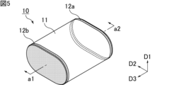
- FIG. 5 is a schematic diagram showing an example of the capacitor element shown in FIGS. 1, 2, 3, and 4 in a perspective view.
- FIG. 6 is a schematic diagram showing an example of a cross section of the capacitor element shown in FIG. 5 along line segment a1-a2.
- FIG. 1 is a schematic diagram showing a perspective view of an example of a capacitor of the present invention.
- FIG. 2 is a schematic diagram showing the capacitor shown in FIG. 1 viewed from a different direction from that shown in FIG.
- FIG. 7 is a schematic diagram showing a perspective view of another example of the capacitor of the present invention.
- FIG. 8 is a schematic diagram showing the capacitor shown in FIG. 7 viewed from the first surface side of the outer case.
- FIG. 9 is a schematic diagram showing a perspective view of an example of the capacitor bank of the present invention.
- FIG. 10 is a schematic diagram showing the capacitor bank shown in FIG. 9 viewed from a different direction from that shown in FIG.
- FIG. 11 is a schematic diagram showing the capacitor bank shown in FIGS. 9 and 10 viewed from the second surface side of the exterior case.
- FIG. 12 is a schematic diagram showing a part of the capacitor bank shown in FIG. 10 in an enlarged view.
- FIG. 13 is a schematic diagram showing a part of the capacitor bank shown in FIG. 12 as viewed from the first surface side of the exterior case.
- the present invention is not limited to the following configuration, and may be modified as appropriate without departing from the gist of the present invention. Furthermore, the present invention also includes a combination of a plurality of individual preferred configurations described below.
- a film capacitor will be shown below as an example of the capacitor of the present invention.
- the capacitor of the present invention is also applicable to capacitors other than film capacitors.
- the capacitor of the present invention includes a capacitor element having an element body and an external electrode provided on an end face of the element body, the capacitor element being electrically connected to the external electrode, and the capacitor element being mounted on an object.
- a pull-out terminal for welding connection an exterior case in which the capacitor element is housed so that the pull-out terminal projects toward the outside, and an outer case filled with the capacitor element so as to be buried therein.
- the outer surface of the outer case includes a mounting surface that faces the mounting object in a first direction when the lead-out terminal is welded and connected to the mounting object; is provided with a mounting mounting leg for welding the exterior case to the mounting object on the mounting surface side, and the mounting mounting leg is electrically insulated from the lead-out terminal, and It is characterized by being made of the same kind of metal material as the lead-out terminal.
- the capacitor exterior case used in the capacitor of the present invention which will be explained below, is also one of the present inventions. That is, the exterior case for a capacitor of the present invention includes a capacitor element having an element body and an external electrode provided on an end face of the element body, the capacitor element being electrically connected to the external electrode, and including the capacitor element.
- An exterior case for a capacitor for storing the capacitor element therein so that the output terminal protrudes outward with respect to an output terminal for welding and connecting the capacitor element to an object to be mounted comprising:
- the outer surface of the outer case includes a mounting surface that faces the mounting object in a first direction when the lead-out terminal is welded to the mounting object, and the outer surface of the outer case includes a mounting surface that faces the mounting object in a first direction when the lead-out terminal is welded to the mounting object. It is characterized in that a mounting mounting leg for welding connection to the mounting object is provided on the side.
- FIG. 1 is a schematic diagram showing a perspective view of an example of the capacitor of the present invention.
- FIG. 2 is a schematic diagram showing the capacitor shown in FIG. 1 viewed from a different direction from that shown in FIG.
- FIG. 3 is a schematic diagram showing the capacitor shown in FIGS. 1 and 2 viewed from a different direction from FIGS. 1 and 2.
- FIG. 4 is a schematic diagram showing the capacitor shown in FIGS. 1, 2, and 3 viewed from the second surface side of the outer case.
- the capacitor 1A shown in FIGS. 1, 2, 3, and 4 includes a capacitor element 10 (see FIG. 5 described later), a first lead terminal 20a, a second lead terminal 20b, and an exterior case 30A. It has a filled resin 40.
- the first direction D1, the second direction D2, and the third direction D3 are orthogonal to each other.
- FIG. 5 is a schematic diagram showing a perspective view of an example of the capacitor element shown in FIGS. 1, 2, 3, and 4.
- FIG. 6 is a schematic diagram showing an example of a cross section of the capacitor element shown in FIG. 5 along line segment a1-a2.
- the capacitor element 10 shown in FIGS. 5 and 6 includes an element body 11, a first external electrode 12a, and a second external electrode 12b.
- the element body 11 is a wound body formed by winding a first metallized film 13a and a second metallized film 13b in a laminated state in the first direction D1. That is, the capacitor 1A, more specifically, the capacitor element 10, is a wound-type film capacitor in which metalized films are laminated and wound.
- the capacitor 1A may be a laminated film capacitor in which metalized films are laminated.
- the cross-sectional shape of the element body 11 is flat when viewed in a cross section perpendicular to the winding axis direction (third direction D3 in FIG. 5). It is preferable. More specifically, it is preferable that the cross-sectional shape of the element body 11 is pressed into a flat shape such as an ellipse or an ellipse, and the thickness is smaller than when the cross-sectional shape of the element body 11 is a perfect circle. .
- the capacitor element 10 may have a cylindrical winding axis.
- the winding axis is arranged on the central axis of the first metallized film 13a and the second metallized film 13b in a wound state, and is used to wind the first metallized film 13a and the second metallized film 13b. This serves as the winding shaft when doing so.
- the first metallized film 13a includes a first dielectric film 14a and a first metal layer 15a.
- the first dielectric film 14a has a first main surface 14aa and a second main surface 14ab that face each other in the first direction D1.
- the first metal layer 15a is provided on the first main surface 14aa of the first dielectric film 14a. More specifically, the first metal layer 15a reaches one side edge of the first dielectric film 14a in the third direction D3 on the first main surface 14aa of the first dielectric film 14a, and extends along the first main surface 14aa of the first dielectric film 14a. It is provided so as not to reach the other side edge of the dielectric film 14a.
- the second metallized film 13b includes a second dielectric film 14b and a second metal layer 15b.
- the second dielectric film 14b has a first main surface 14ba and a second main surface 14bb that face each other in the first direction D1.
- the second metal layer 15b is provided on the first main surface 14ba of the second dielectric film 14b. More specifically, the second metal layer 15b does not reach one side edge of the second dielectric film 14b in the third direction D3 on the first main surface 14ba of the second dielectric film 14b, It is provided so as to reach the other side edge of the second dielectric film 14b.
- the end of the first metal layer 15a that reaches the side edge of the first dielectric film 14a is exposed on one end surface of the element body 11, and the second dielectric layer in the second metal layer 15b
- the adjacent first metallized film 13a and second metallized film 13b are shifted in the third direction D3 so that the end reaching the side edge of the film 14b is exposed to the other end surface of the element body 11.
- the first metallized film 13a protrudes toward the first external electrode 12a with respect to the second metallized film 13b.
- the second metallized film 13b projects toward the second external electrode 12b with respect to the first metallized film 13a.
- the first metal layer 15a is connected to the first external electrode 12a and not connected to the second external electrode 12b.
- the second metal layer 15b is connected to the second external electrode 12b and not connected to the first external electrode 12a.
- the adjacent first metallized film 13a and the second metallized film 13b are shifted in the third direction D3 as described above, the adjacent first dielectric film 14a and the second dielectric film 14b, the first dielectric film 14a in which the first metal layer 15a is provided on the first main surface 14aa is different from the second dielectric film 14b in which the first metal layer 15a is not provided on the main surface. and protrudes toward the first external electrode 12a.
- the second dielectric film 14b in which the second metal layer 15b is provided on the first main surface 14ba has the second metal layer 15b on the first main surface 14ba. It protrudes toward the second external electrode 12b with respect to the first dielectric film 14a that is not provided on the main surface.
- the element body 11 is formed by winding the first metallized film 13a and the second metallized film 13b in a laminated state in the first direction D1, the first dielectric film 14a and the first metal layer 15a , the second dielectric film 14b, and the second metal layer 15b in order in the first direction D1. Moreover, the element body 11 is wound in a state in which the first dielectric film 14a, the first metal layer 15a, the second dielectric film 14b, and the second metal layer 15b are laminated in order in the first direction D1. It can also be said that it is a rolled body.
- the first main surface 14aa of the first dielectric film 14a and the second main surface 14bb of the second dielectric film 14b face each other in the first direction D1
- the second main surface 14ab and the first main surface 14ba of the second dielectric film 14b face each other in the first direction D1.
- the first metallized film 13a and the second metallized film 13b are wound in a laminated state in the first direction D1.
- the second metallized film 13b is inside the first metallized film 13a, and more specifically, the first metal layer 15a is inside the first dielectric film 14a, and The first metallized film 13a and the second metallized film 13b are laminated and wound in the first direction D1 so that the second metal layer 15b is located inside the second dielectric film 14b. That is, in the element body 11, the first metal layer 15a and the second metal layer 15b face each other with the first dielectric film 14a or the second dielectric film 14b in between.
- a fuse portion may be provided in the first metal layer 15a.
- the fuse portion provided in the first metal layer 15a includes, for example, a divided electrode portion in which a portion of the first metal layer 15a that faces the second metal layer 15b is divided into a plurality of parts, and a portion that does not face the second metal layer 15b. This is the part that connects the electrode section.
- Examples of the electrode pattern of the first metal layer 15a provided with the fuse portion include the electrode patterns disclosed in JP-A-2004-363431, JP-A-5-251266, and the like.
- the second metal layer 15b may also be provided with a fuse portion.
- the first dielectric film 14a may contain a curable resin as a main component.
- the main component means the component with the highest weight percentage, preferably the component with the weight percentage higher than 50% by weight.
- the curable resin may be a thermosetting resin or a photocurable resin.
- thermosetting resin means a resin that can be cured by heat, but the curing method thereof is not limited. Therefore, thermosetting resins include resins that can be cured by methods other than heat (eg, light, electron beam, etc.) as long as they can be cured by heat. Further, depending on the material, a reaction may start due to the reactivity of the material itself, and a resin that hardens even without necessarily applying heat or the like from the outside is also referred to as a thermosetting resin. The same applies to photocurable resins, and as long as the resins can be cured by light, resins that can be cured by methods other than light (for example, heat, etc.) are also included.
- the curable resin is preferably made of a cured product of a first organic material having a hydroxyl group (OH group) and a second organic material having an isocyanate group (NCO group).
- the curable resin is a cured product having urethane bonds obtained by the reaction of the hydroxyl groups of the first organic material and the isocyanate groups of the second organic material.
- FT-IR Fourier transform infrared spectrophotometer
- the first dielectric film 14a may contain at least one of a hydroxyl group and an isocyanate group.
- the first dielectric film 14a may contain one of a hydroxyl group and an isocyanate group, or may contain both a hydroxyl group and an isocyanate group.
- Examples of the first organic material include phenoxy resin, polyvinyl acetoacetal resin, polyvinyl butyral resin, and the like.
- the first organic material multiple types of organic materials may be used together.
- the second organic material examples include aromatic polyisocyanates such as diphenylmethane diisocyanate (MDI) and tolylene diisocyanate (TDI), and aliphatic polyisocyanates such as hexamethylene diisocyanate (HDI).
- aromatic polyisocyanates such as diphenylmethane diisocyanate (MDI) and tolylene diisocyanate (TDI)
- aliphatic polyisocyanates such as hexamethylene diisocyanate (HDI).
- HDI hexamethylene diisocyanate
- the second organic material multiple types of organic materials may be used together.
- the first dielectric film 14a may contain thermoplastic resin as a main component.
- thermoplastic resin examples include polypropylene, polyether sulfone, polyetherimide, polyarylate, and the like.
- the first dielectric film 14a may contain additives for adding various functions.
- additives include leveling agents for imparting smoothness.
- the additive preferably has a functional group that reacts with a hydroxyl group and/or an isocyanate group and forms a part of the crosslinked structure of the cured product.
- examples of such additives include resins having at least one functional group selected from the group consisting of hydroxyl groups, epoxy groups, silanol groups, and carboxyl groups.
- the second dielectric film 14b may also contain a curable resin as a main component, or may contain a thermoplastic resin as a main component. Further, the second dielectric film 14b may also contain additives, similar to the first dielectric film 14a.
- compositions of the first dielectric film 14a and the second dielectric film 14b may be different from each other, but are preferably the same.
- the thickness of the first dielectric film 14a and the second dielectric film 14b is preferably 1 ⁇ m or more and 10 ⁇ m or less, more preferably 3 ⁇ m or more and 5 ⁇ m or less.
- the thicknesses of the first dielectric film 14a and the second dielectric film 14b may be different from each other, but are preferably the same.
- the thickness of the dielectric film is measured using an optical film thickness meter.
- the first dielectric film 14a and the second dielectric film 14b are each preferably produced by molding a resin solution containing the above-mentioned resin material into a film shape and then curing it by heat treatment.
- Examples of the constituent materials of the first metal layer 15a and the second metal layer 15b include metals such as aluminum, zinc, titanium, magnesium, tin, and nickel.
- compositions of the first metal layer 15a and the second metal layer 15b may be different from each other, but are preferably the same.
- the thickness of the first metal layer 15a and the second metal layer 15b is preferably 5 nm or more and 40 nm or less.
- the thicknesses of the first metal layer 15a and the second metal layer 15b may be different from each other, but are preferably the same.
- the thickness of the metal layer is measured by observing a cross section of the metallized film along the first direction using a transmission electron microscope (TEM).
- TEM transmission electron microscope
- the first metal layer 15a and the second metal layer 15b are each preferably formed by depositing the metal as described above on the main surfaces of the first dielectric film 14a and the second dielectric film 14b.
- the first external electrode 12a is provided on one end surface of the element body 11. More specifically, the first external electrode 12a is connected to the first metal layer 15a by contacting the end of the first metal layer 15a exposed on one end surface of the element body 11. On the other hand, the first external electrode 12a is not connected to the second metal layer 15b.
- the second external electrode 12b is provided on the other end surface of the element body 11. More specifically, the second external electrode 12b is connected to the second metal layer 15b by contacting the end of the second metal layer 15b exposed on the other end surface of the element body 11. On the other hand, the second external electrode 12b is not connected to the first metal layer 15a.
- Examples of the constituent material of the first external electrode 12a and the second external electrode 12b include metals such as zinc, aluminum, tin, and zinc-aluminum alloy.
- compositions of the first external electrode 12a and the second external electrode 12b may be different from each other, but are preferably the same.
- the first external electrode 12a and the second external electrode 12b are preferably formed by spraying the metal as described above onto one end surface and the other end surface of the element body 11, respectively.
- the first lead terminal 20a is electrically connected to the first external electrode 12a (see FIGS. 5 and 6).
- the first lead terminal 20a is electrically connected to the first external electrode 12a via a joining member such as solder.
- the second lead terminal 20b is electrically connected to the second external electrode 12b (see FIGS. 5 and 6).
- the second lead terminal 20b is electrically connected to the second external electrode 12b via a joining member such as solder.
- the first lead-out terminal 20a and the second lead-out terminal 20b are lead-out terminals for welding and connecting the capacitor element 10 to the mounting target, respectively.
- the capacitor 1A When mounting the capacitor 1A on an object to be mounted, in order to connect the first drawer terminal 20a and the second drawer terminal 20b to the object to be mounted by welding, the first drawer terminal 20a and the second drawer terminal 20b are fastened with screws,
- the capacitor 1A, especially the capacitor element 10 can be firmly fixed to the mounting object compared to the case where it is fixed to the mounting object by soldering or the like. Thereby, the vibration and shock resistance of the capacitor 1A mounted on the object can be improved.
- the first lead-out terminal 20a and the second lead-out terminal 20b are welded and connected to the mounting target, so that the connection between the first lead-out terminal 20a and the mounting target is The resistance and the connection resistance between the second lead-out terminal 20b and the mounting object can be reduced. Thereby, the conductivity between the capacitor 1A and the object to be mounted can be improved.
- the shapes of the first pull-out terminal 20a and the second pull-out terminal 20b may each be, for example, plate-shaped or linear (rod-shaped). In this case, each of the first extraction terminal 20a and the second extraction terminal 20b may have a partially bent shape.
- the capacitor element 10 (see FIGS. 5 and 6) is housed inside the exterior case 30A so that the first pull-out terminal 20a and the second pull-out terminal 20b protrude toward the outside. Although not shown in FIG. 1 etc., it is preferable that the capacitor element 10 is housed in the center of the interior of the exterior case 30A while being separated from the inner surface of the exterior case 30A.
- the shape of the exterior case 30A is, for example, a bottomed cylindrical shape with an opening 31 provided at one end in the second direction D2, as shown in FIG. 1 and the like.
- the outer surface of the exterior case 30A includes a first surface 32 facing the opening 31 in the second direction D2, and a second surface extending from the first surface 32 toward the opening 31 in the second direction D2. 33 (including four surfaces in the example shown in FIG. 1 etc.).
- Examples of the exterior case 30A include a resin case, a metal case, and the like.
- the exterior case 30A is a resin case
- the resin constituting the resin case examples include liquid crystal polymer (LCP), polyphenylene sulfide, polybutylene terephthalate, and the like.
- LCP liquid crystal polymer
- the resin case contains a liquid crystal polymer.
- liquid crystal polymer contained in the resin case for example, a liquid crystal polymer having p-hydroxybenzoic acid and 6-hydroxy-2-naphthoic acid groups in its skeleton is used. Furthermore, in addition to p-hydroxybenzoic acid and 6-hydroxy-2-naphthoic acid groups, liquid crystal polymers formed into polycondensates using various components such as phenol, phthalic acid, and ethylene terephthalate can be used. Further, when classifying liquid crystal polymers, there are classification methods such as type I, type II, and type III, but the material means the same material as the liquid crystal polymer formed from the above-mentioned components.
- the resin case further contains an inorganic filler in addition to the liquid crystal polymer.
- the inorganic filler contained in the resin case a material with higher strength than liquid crystal polymer can be used.
- the inorganic filler is preferably a material with a melting point higher than that of the liquid crystal polymer, and more preferably a material with a melting point of 680° C. or higher.
- the form of the inorganic filler is not particularly limited, and examples thereof include forms having a longitudinal direction such as fibrous or plate-like forms. As such a form of inorganic filler, a plurality of types of inorganic materials may be used together. It is preferable that the resin case contains at least one of a fibrous inorganic material and a plate-like inorganic material as an inorganic filler.
- the term ⁇ the filler is fibrous'' means that in the filler, the relationship between the longitudinal dimension and the cross-sectional diameter in a cross section perpendicular to the longitudinal direction is 5 (i.e., aspect ratio). means a state in which the ratio is 5:1 or more).
- the cross-sectional diameter is the longest distance between two points on the outer circumference of the cross-section. If the cross-sectional diameter differs in the longitudinal direction, measure at the point where the cross-sectional diameter is maximum.
- the cross-sectional diameter/maximum height when the filling material is plate-shaped, the relationship between the cross-sectional diameter of the surface with the largest projected area and the maximum height in the direction orthogonal to this cross-section is defined as the cross-sectional diameter/maximum height. It means a state in which the value is 3.
- At least a portion of the inorganic filler is oriented toward the second surface 33 of the outer case 30A, in a portion oriented from the first surface 32 toward the opening 31 and toward the adjacent second surface 33. It is preferable that the outer case 30A has a plurality of portions and is dispersed inside the outer case 30A.
- the size of the inorganic filler is preferably 5 ⁇ m or more in diameter and 50 ⁇ m or more in length.
- the inorganic filler is dispersed throughout the exterior case 30A without agglomerating.
- the inorganic filler examples include inorganic materials such as fibrous glass filler, plate-shaped talc, or mica. Among these, it is preferable that the inorganic filler contains fibrous glass filler as a main component.
- the resin case contains another resin (for example, polyphenylene sulfide) instead of the liquid crystal polymer, it is preferable that the resin case further contains an inorganic filler as described above.
- another resin for example, polyphenylene sulfide
- the resin case further contains an inorganic filler as described above.
- the resin case is manufactured, for example, by a method such as injection molding.
- the exterior case 30A is a metal case
- the metal constituting the metal case include simple metals such as aluminum, magnesium, iron, stainless steel, and copper, and alloys containing at least one of these simple metals. It will be done. Among these, it is preferable that the metal case contains aluminum or an aluminum alloy.
- the metal case is manufactured, for example, by a method such as impact molding.
- one capacitor element 10 is housed inside one exterior case 30A, but a plurality of capacitor elements 10 are housed inside one exterior case 30A. Good too.
- the filling resin 40 is filled in the exterior case 30A so as to bury the capacitor element 10. By being filled with the filling resin 40 in this manner, the capacitor element 10 is held inside the exterior case 30A.
- the filling resin 40 is placed between the capacitor element 10 and the outer case 30A, more specifically, between the capacitor element 10 and the outer case 30A. is filled between the outer surface of the outer case 30A and the inner surface of the outer case 30A. Further, the filling resin 40 is filled inside the exterior case 30A, not only between the capacitor element 10 and the exterior case 30A, but also in a region extending from the opening 31 of the exterior case 30A to the capacitor element 10.
- the filling resin 40 from the viewpoint of suppressing the infiltration of moisture into the capacitor element 10, it is preferable to appropriately select a resin with low moisture permeability, and examples thereof include epoxy resin, silicone resin, urethane resin, and the like.
- examples of curing agents for epoxy resins include amine curing agents and imidazole curing agents.
- the filling resin 40 only the resin mentioned above may be used, but a reinforcing agent may be added to the resin for the purpose of improving the strength.
- a reinforcing agent include silica and alumina.
- the thickness of the filling resin 40 in the opening 31 of the outer case 30A is large.
- the thickness of the filling resin 40 in the opening 31 of the outer case 30A is preferably large enough within the allowable range of the entire volume (physique) of the capacitor 1A, specifically, preferably 2 mm or more, more preferably 4 mm or more. be.
- the thickness of the filling resin 40 to the capacitor element 10 can be reduced by the opening 31 of the outer case 30A. It is preferable to make it larger on the side than on the first surface 32 side.
- the thickness of the filled resin 40 is measured using a soft X-ray device if it is in a non-destructive state, and is measured using a length measuring device such as a caliper if it is in a destructive state.
- the relationship between the height of the outer case 30A and the height of the filled resin 40 in the second direction D2 is such that the thickness of the filled resin 40 at the opening 31 of the outer case 30A is made as large as possible, and the position inside the outer case 30A is It may be up to a maximum, it may be about a full cup, or it may be slightly overflowing due to surface tension.
- the outer surface of the exterior case 30A includes a mounting surface 34 that faces the mounting target in the first direction D1 when the first pull-out terminal 20a and the second pull-out terminal 20b are welded and connected to the mounting target.
- the outer surface of the exterior case 30A includes a mounting surface 34 as a part of the second surface 33.
- Mounting mounting legs 50 are provided on the outer surface of the exterior case 30A.
- the mounting mounting leg 50 is attached to the first rib 35a provided on the outer surface of the exterior case 30A, here the mounting surface 34 (second surface 33). In this way, in the example shown in FIG. 1 and the like, mounting mounting legs 50 are provided on the mounting surface 34 of the exterior case 30A.
- the mounting mounting leg 50 is attached to the first rib 35a by, for example, insert molding or the like.
- the shape of the first rib 35a is not particularly limited.
- first rib 35a may not be provided on the outer surface of the exterior case 30A. That is, the location where the mounting mounting leg 50 is provided is not limited to the first rib 35a of the exterior case 30A.
- the mounting mounting leg 50 is a mounting leg for welding the exterior case 30A to the mounting target on the mounting surface 34 side.
- the mounting mounting legs 50 When mounting the capacitor 1A on the mounting object, the mounting mounting legs 50 are welded and connected to the mounting object, so there are cases where the mounting mounting legs 50 are fixed to the mounting object by screwing, soldering, etc.
- the capacitor 1A, especially the outer case 30A can be firmly fixed to the mounting target. Thereby, the vibration and shock resistance of the capacitor 1A mounted on the object can be improved.
- the mounting mounting legs 50 are attached to the mounting object in the same process as welding and connecting the first extraction terminal 20a and the second extraction terminal 20b to the mounting object. Can be connected by welding.
- the conventional fixing process such as fixing the capacitor to the mounting target by screwing etc. is not necessary, which is necessary for fixing the capacitor to the mounting target. Time, cost, etc. can be reduced.
- the mounting mounting leg 50 is electrically insulated from the first extraction terminal 20a and the second extraction terminal 20b. That is, in the capacitor 1A, the mounting mounting leg 50 is electrically insulated from the capacitor element 10 to which the first extraction terminal 20a and the second extraction terminal 20b are electrically connected.
- the mounting mounting leg 50 is made of the same kind of metal material as the first pull-out terminal 20a and the second pull-out terminal 20b. Thereby, when mounting the capacitor 1A on the mounting object, the mounting mounting leg 50 can be welded and connected to the mounting object using the same welding method as the first pull-out terminal 20a and the second pull-out terminal 20b.
- the expression that a plurality of members are made of the same type of metal material means that the types of metal elements that are the basic components of the metal materials are the same.
- the basic component of the metal material may be composed of only one type of metal element, or may be composed of multiple types of metal elements.
- the metal elements of the basic components of the metal material constituting one member are E1 and E2
- the basic metallic elements of the metallic material constituting the other member are E1 and E2
- both members are composed of the same kind of metallic material. The same applies when comparing three or more members.
- the content of the basic components in the metal material may be the same, different, or partially different among the plurality of members.
- the weight ratios of the multiple metal elements in the basic component may be the same or different between the multiple members. , may differ in some parts.
- the metal material may also contain 1% by weight or less of additional components.
- the types of metal elements that are additive components of the metal material may be the same, different, or partially different among the plurality of members.
- the additive component of the metal material may be composed of only one type of metal element, or may be composed of multiple types of metal elements.
- the content of the additive component in the metal material may be the same, different, or partially different between the plurality of members.
- the weight ratio of the multiple metal elements in the additive component may be the same or different between the multiple members. , may differ in some parts.
- the metal material does not need to contain any additive components.
- the metal materials of all members may contain the additive component, the metal materials of some members may contain the additive component, or the metal materials of all the members may contain the additive component. It does not have to contain.
- Examples of the metal material constituting the first pull-out terminal 20a, the second pull-out terminal 20b, and the mounting mounting leg 50 include copper, oxygen-free copper, aluminum, and an alloy containing at least one of these. . Among these, it is preferable that the metal material constituting the first lead-out terminal 20a, the second lead-out terminal 20b, and the mounting mounting leg 50 is copper or oxygen-free copper.
- the metal material constituting the first extraction terminal 20a, the second extraction terminal 20b, and the mounting mounting leg 50 is a copper-based material, for example, oxygen-free copper (copper: 99.96% by weight or more), tough pitch copper (copper: 99.90% by weight or more), phosphorus deoxidized copper (copper: 99.90% by weight or more, phosphorus: 0.015% by weight or more and 0.040% by weight or less), etc. can be used.
- a welding method such as laser welding or resistance welding is used.
- laser welding has the advantage that welding can be performed in a short time by local heating, and welding distortion can be reduced.
- the mounting mounting legs 50 protrude beyond the mounting surface 34 of the exterior case 30A in the first direction D1.
- a gap can be provided between the mounting surface 34 of the outer case 30A and the mounting object while the capacitor 1A is mounted on the mounting object.
- the gap provided between the mounting surface 34 of the outer case 30A and the mounting target is filled with heat dissipation paste, underfill adhesive (e.g. containing epoxy resin). It can be used as a location for connecting members such as adhesives.
- the capacitor 1A can be firmly fixed to the object to be mounted.
- first lead-out terminal 20a and the second lead-out terminal 20b each protrude beyond the mounting surface 34 of the exterior case 30A in the first direction D1.
- the distance between the mounting surface 34 of the outer case 30A and the mounting object is the distance between the first pull-out terminal 20a, the second pull-out terminal 20b, and the mounting mounting leg 50. can be adjusted by the shape of the
- a space F is provided between the mounting surface 34 of the exterior case 30A and the mounting mounting leg 50.
- a space F is provided between the first surface 35aa of the first rib 35a included in the mounting surface 34 of the exterior case 30A and the mounting mounting leg 50.
- a laser beam is irradiated to the welding part of the mounting mounting leg 50 during laser welding, or an electrode is used during resistance welding. Welding work such as contacting the mounting mounting leg 50 becomes easier.
- the distance between the mounting surface 34 of the exterior case 30A and the mounting mounting leg 50 can be adjusted depending on the shape of the mounting mounting leg 50.
- the space F does not need to be provided between the mounting surface 34 of the exterior case 30A and the mounting mounting leg 50.
- the mounting legs 50 for mounting may be provided along the mounting surface 34 of the outer case 30A so as to be in contact with the mounting surface 34 of the outer case 30A.
- the mounting mounting legs 50 do not protrude from the exterior case 30A when viewed from the first direction D1.
- the mounting mounting legs 50 for mounting do not protrude from the outer case 30A
- the mounting area of the capacitor 1A is Can be reduced.
- the mounting mounting legs 50 do not protrude from the exterior case 30A when viewed from the first direction D1 compared to the case where the mounting mounting legs 50 protrude from the exterior case 30A, for example, a plurality of When the capacitors 1A are arranged and mechanically connected in a direction perpendicular to the first direction D1 (in the example shown in FIG. 1, a direction including the second direction D2 and the third direction D3), adjacent capacitors 1A are Less likely to interfere.
- the mounting mounting legs 50 may protrude from the exterior case 30A when viewed from the first direction D1. In this case, since the part of the mounting leg 50 protruding from the outer case 30A can be used as a welding part, there is no space between the mounting surface 34 of the outer case 30A and the mounting leg 50. It's okay.
- the shape of the mounting mounting leg 50 may be, for example, plate-like or linear (rod-like). In this case, the mounting mounting leg 50 may have a partially bent shape.
- Only one mounting mounting leg 50 may be provided as shown in FIG. 1, etc., or a plurality of mounting mounting legs 50 may be provided.
- FIG. 7 is a schematic diagram showing a perspective view of another example of the capacitor of the present invention.
- FIG. 8 is a schematic diagram showing the capacitor shown in FIG. 7 viewed from the first surface side of the outer case.
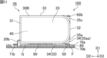
- the capacitor 1B shown in FIGS. 7 and 8 has an outer case 30B instead of the outer case 30A, unlike the capacitor 1A shown in FIG. 1, etc.
- a first fixing mounting leg 60a and a second fixing mounting leg 60b are further provided on the outer surface of the exterior case 30B.
- the first fixing mounting leg 60a is attached to the second rib 35b provided on the outer surface of the exterior case 30B, here the second surface 33.
- the first fixing mounting leg 60a is attached to the second rib 35b, for example, by a method such as insert molding.
- the second fixing mounting leg 60b is attached to the third rib 35c provided on the outer surface of the exterior case 30B, here the second surface 33.
- the second fixing mounting leg 60b is attached to the third rib 35c, for example, by a method such as insert molding.
- the shapes of the second rib 35b and the third rib 35c are not particularly limited.
- the second rib 35b and the third rib 35c may not be provided on the outer surface of the exterior case 30B. That is, the location where the fixing mounting leg 60 is provided is not limited to the second rib 35b and the third rib 35c of the exterior case 30B.
- the first fixing mounting leg 60a and the second fixing mounting leg 60b are mounting legs for welding and connecting the exterior case 30B to another exterior case.
- the first fixing mounting leg 60a is provided at a different position from the mounting mounting leg 50 so as to be electrically insulated from the first extraction terminal 20a and the second extraction terminal 20b. That is, the first fixing mounting leg 60a is electrically insulated from the capacitor element 10 to which the first extraction terminal 20a and the second extraction terminal 20b are electrically connected.
- the second fixing mounting leg 60b is provided at a different position from the mounting mounting leg 50 so as to be electrically insulated from the first extraction terminal 20a and the second extraction terminal 20b.
- the second fixing mounting leg 60b is electrically insulated from the capacitor element 10 to which the first extraction terminal 20a and the second extraction terminal 20b are electrically connected.
- first fixing mounting leg 60a and the second fixing mounting leg 60b are electrically insulated from each other.
- first fixing mounting leg 60a and the second fixing mounting leg 60b are each electrically insulated from the mounting mounting leg 50.
- first fixing mounting leg 60a and the second fixing mounting leg 60b are made of the same kind of metal material as the first pull-out terminal 20a and the second pull-out terminal 20b. That is, it is preferable that the first fixing mounting leg 60a and the second fixing mounting leg 60b are made of the same type of metal material as the mounting mounting leg 50. In this case, the first fixing mounting leg 60a and the second fixing mounting leg 60a are attached using the same welding method used when welding the first pull-out terminal 20a, the second pull-out terminal 20b, and the mounting mounting leg 50 to the mounting object. It can be connected to the leg 60b by welding.
- Examples of the metal material constituting the first fixing mounting leg 60a and the second fixing mounting leg 60b include copper, oxygen-free copper, aluminum, and an alloy containing at least one of these. Among these, it is preferable that the metal material forming the first fixing mounting leg 60a and the second fixing mounting leg 60b is copper or oxygen-free copper.
- the metal material constituting the first fixing mounting leg 60a and the second fixing mounting leg 60b is a copper-based material
- oxygen-free copper copper: 99.96% by weight or more
- tough pitch copper copper: 99.9% by weight or more
- .90% by weight or more phosphorus deoxidized copper
- phosphorus: 0.015% by weight or more, 0.040% by weight or less etc.
- a welding method such as laser welding or resistance welding is used.
- the mounting mounting leg 50 and the first fixing mounting leg 60a are preferably provided at different height positions in the first direction D1. Further, as shown in FIG. 7 and the like, the mounting mounting leg 50 and the second fixing mounting leg 60b are preferably provided at different height positions in the first direction D1.
- each capacitor 1B when a plurality of capacitors 1B are mechanically connected and mounted on a mounting target, each capacitor 1B, especially each outer case 30B, can be fixed at multiple locations at different height positions. The vibration and shock resistance can be sufficiently improved when the capacitor 1B is mechanically connected.
- the first fixing mounting leg 60a and the second fixing mounting leg 60b may be provided at the same height position in the first direction D1, or may be provided at different height positions in the first direction D1. It's okay.
- first fixing mounting leg 60a and the second fixing mounting leg 60b are provided at different height positions in the first direction D1, as shown in FIG. 13 described later, the first fixing mounting leg 60a
- the surfaces of the second fixing mounting legs 60b facing each other in the first direction D1 can be easily welded and connected to each other.
- the mounting mounting leg 50 and the first fixing mounting leg 60a extend in mutually different directions. Furthermore, as shown in FIG. 7 etc., it is preferable that the mounting mounting leg 50 and the second fixing mounting leg 60b extend in mutually different directions. In this case, it becomes easier to weld and connect the first fixing attaching leg 60a and the second fixing attaching leg 60b while welding the mounting attaching leg 50 to the mounting target.
- the mounting mounting legs 50 for mounting and the first mounting legs 60a for fixing extend in different directions
- the mounting mounting legs 50 for mounting and the first mounting legs 60a for fixing extend in directions that are orthogonal to the first direction D1 and intersect with each other. It may extend to Furthermore, when the mounting mounting legs 50 for mounting and the second mounting legs 60b for fixing extend in different directions, the mounting mounting legs 50 for mounting and the second mounting legs 60b for fixing cross each other while being perpendicular to the first direction D1. It may extend in the direction.
- the mounting mounting leg 50 may extend in the second direction D2
- the first fixing mounting leg 60a and the second fixing mounting leg 60b may extend in the third direction D3.
- the mounting mounting legs 50 are welded and connected to the mounting object, and the first fixing mounting legs 60a and the second fixing mounting legs 60b are connected. Easier to weld connections.
- mounting mounting leg 50 and the first fixing mounting leg 60a do not have to extend in directions perpendicular to each other. Further, the mounting mounting leg 50 and the second fixing mounting leg 60b do not need to extend in directions perpendicular to each other.
- first fixing mounting leg 60a and the second fixing mounting leg 60b may be, for example, plate-shaped or linear (rod-shaped). In this case, each of the first fixing mounting leg 60a and the second fixing mounting leg 60b may have a partially bent shape.
- Only one first fixing mounting leg 60a and second fixing mounting leg 60b may be provided, as shown in FIG. 7, etc., or a plurality of them may be provided.
- the capacitor bank of the present invention is characterized by comprising the capacitor of the present invention, and the mounting object to which the lead-out terminal and mounting leg of the capacitor are welded and connected.
- FIG. 9 is a schematic diagram showing a perspective view of an example of the capacitor bank of the present invention.
- FIG. 10 is a schematic diagram showing the capacitor bank shown in FIG. 9 viewed from a different direction from that shown in FIG.
- FIG. 11 is a schematic diagram showing the capacitor bank shown in FIGS. 9 and 10 viewed from the second surface side of the exterior case.
- the capacitor bank 100 shown in FIGS. 9, 10, and 11 includes a plurality of capacitors 1B (see FIGS. 7 and 8), a first bus bar 70a, and a second bus bar 70b.
- the first bus bar 70a and the second bus bar 70b are included in a mounting object on which a plurality of capacitors 1B are mounted.
- the first bus bar 70a and the second bus bar 70b are stacked in the first direction D1. More specifically, the first bus bar 70a is provided closer to the capacitor 1B than the second bus bar 70b in the first direction D1. In other words, the second bus bar 70b is provided on the opposite side of the capacitor 1B from the first bus bar 70a in the first direction D1.
- Examples of the constituent material of the first bus bar 70a and the second bus bar 70b include metals such as copper.
- An insulating member 80 is provided between the first bus bar 70a and the second bus bar 70b to ensure insulation between them.
- Examples of the constituent material of the insulating member 80 include resin.
- the first bus bar 70a and the insulating member 80 are both hollowed out in some areas.
- the second bus bar 70b is exposed from the first bus bar 70a and the insulating member 80 as an exposed portion 71b.
- the plurality of capacitors 1B are each mounted on the mounting object including the first bus bar 70a and the second bus bar 70b on the mounting surface 34 side of the outer case 30B. More specifically, it is as follows.
- the first lead terminal 20a is welded to the first bus bar 70a, and the second lead terminal 20b is connected to the second bus bar 70b, here, the second bus bar 70b. It is welded and connected to the exposed portion 71b.
- the mounting mounting leg 50 is welded and connected to the first bus bar 70a. In the state of the capacitor 1B alone, the mounting mounting leg 50 is electrically insulated from the first lead-out terminal 20a, but in the state of the capacitor bank 100, the mounting mounting leg 50 is electrically insulated from the first lead-out terminal 20a through the first bus bar 70a. It will be electrically connected to the first extraction terminal 20a.
- each capacitor 1B is connected to the mounting target including the first bus bar 70a and the second bus bar 70b. is welded to the Therefore, in the capacitor bank 100, each capacitor 1B is firmly fixed to the mounting target. This improves the vibration and shock resistance of the capacitor bank 100 in which a plurality of capacitors 1B are mounted on an object.
- the capacitor bank 100 having the above-described configuration can be manufactured at low cost.
- the first lead-out terminal 20a, the second lead-out terminal 20b, and the mounting mounting leg 50 of each capacitor 1B are connected to the mounting surface 30 of the exterior case 30B in the first direction D1. It is preferable that it protrude more than that.
- a gap G is provided between the mounting surface 34 of the exterior case 30B of each capacitor 1B and the mounting target, here the first bus bar 70a.
- the connection member 90 is preferably provided in the gap G so as to be in contact with the mounting surface 34 of the exterior case 30B of each capacitor 1B and the first bus bar 70a. .
- each capacitor 1B and the first bus bar 70a are also connected via the connecting member 90.
- a heat dissipation paste is used as the connection member 90, it becomes easy to achieve the desired heat dissipation performance of each capacitor 1B.
- an underfill adhesive is used as the connecting member 90, each capacitor 1B, particularly the outer case 30B of each capacitor 1B, can be fixed sufficiently firmly to the first bus bar 70a.
- the plurality of capacitors 1B are mechanically connected. More specifically, it is as follows.
- FIG. 12 is a schematic diagram showing an enlarged view of a part of the capacitor bank shown in FIG. 10.
- FIG. 13 is a schematic diagram showing a part of the capacitor bank shown in FIG. 12 as viewed from the first surface side of the exterior case.
- the first fixing mounting leg 60a of one capacitor 1B and the second fixing mounting leg 60b of the other capacitor 1B are welded. It is connected.
- the first fixing mounting leg 60a and the second fixing mounting leg 60b are provided at different height positions in the first direction D1. The surfaces of the leg 60a and the second fixing mounting leg 60b that face each other in the first direction D1 are welded together.
- adjacent capacitors 1B are welded and connected via the first fixing mounting leg 60a and the second fixing mounting leg 60b. Therefore, in the capacitor bank 100, adjacent capacitors 1B are firmly connected to each other, especially adjacent exterior cases 30B are firmly connected to each other. Thereby, in the capacitor bank 100, the vibration and shock resistance is improved in a state where the plurality of capacitors 1B are mechanically connected.
- the first fixing mounting leg 60a and the second fixing mounting leg 60b are provided at different height positions from the mounting mounting leg 50 in the first direction D1. It is preferable.
- each capacitor 1B, especially each exterior case 30B is fixed at multiple locations at different heights, so the durability of the multiple capacitors 1B in a mechanically connected state is limited. Vibration and impact resistance is sufficiently improved.
- the mounting mounting leg 50 and the first fixing mounting leg 60a preferably extend in different directions. Furthermore, as shown in FIG. 12, in the capacitor bank 100, it is preferable that the mounting mounting leg 50 and the second fixing mounting leg 60b extend in mutually different directions. In this case, when manufacturing the capacitor bank 100, it becomes easier to weld and connect the first fixing attaching leg 60a and the second fixing attaching leg 60b while welding the mounting attaching leg 50 to the first bus bar 70a. .
- the mounting mounting legs 50 extend in the second direction D2, and the first fixing mounting legs 60a and the second fixing mounting legs 60b extend in the third direction D3. good.
- the mounting mounting legs 50 are welded and connected to the mounting object, and the first fixing mounting legs 60a and It becomes easier to weld and connect the second fixing mounting leg 60b.
- the capacitor bank 100 has a plurality of capacitors 1B, the number of capacitors 1B that the capacitor bank 100 has is not limited to six as shown in FIG. 9 and the like.
- the capacitor bank 100 has a plurality of capacitors 1B, it may have only one capacitor 1B.
- capacitor bank 100 all of the plurality of capacitors 1B may be replaced with capacitors 1A (see FIGS. 1, 2, 3, and 4), or some of them may be replaced with capacitors 1A. It's okay.
- bus bars such as the first bus bar 70a and the second bus bar 70b are used as mounting objects, but in addition to bus bars, substrates, casings, etc. may be used as mounting objects.
- the capacitor of the present invention can improve vibration and shock resistance when mounted on an object, it is useful as a smoothing capacitor for automotive applications that particularly requires high vibration and shock resistance.
- the capacitor bank of the present invention can improve vibration and shock resistance when the capacitor of the present invention is mounted on an object, so the capacitor bank of the present invention can improve vibration and shock resistance when the capacitor of the present invention is mounted on an object. , inverters).
- a capacitor element having an element body and an external electrode provided on an end surface of the element body; a lead-out terminal electrically connected to the external electrode and for welding the capacitor element to the mounting target; an exterior case in which the capacitor element is housed so that the extraction terminal protrudes toward the outside; a filled resin filled in the outer case so as to embed the capacitor element;
- the outer surface of the exterior case includes a mounting surface that faces the mounting object in a first direction when the lead-out terminal is welded and connected to the mounting object,
- the outer surface of the outer case is provided with mounting mounting legs for welding the outer case to the mounting object on the mounting surface side,
- a capacitor characterized in that the mounting mounting leg is electrically insulated from the lead-out terminal and made of the same type of metal material as the lead-out terminal.
- ⁇ 3> The capacitor according to ⁇ 2>, wherein a space is provided between the mounting surface of the exterior case and the mounting mounting leg.
- ⁇ 4> The capacitor according to any one of ⁇ 1> to ⁇ 3>, wherein the mounting mounting leg does not protrude from the outer case when viewed from the first direction.
- fixing mounting legs for welding the exterior case to another exterior case are located at different positions from the mounting legs so that the mounting legs are electrically insulated from the lead-out terminals.
- ⁇ 6> The capacitor according to ⁇ 5>, wherein the mounting leg and the fixing leg are provided at different height positions in the first direction.
- the mounting mounting leg extends in a second direction perpendicular to the first direction,
- a capacitor bank comprising: the mounting object to which the extraction terminal of the capacitor and the mounting mounting leg are welded and connected.
- a capacitor element having an element body and an external electrode provided on an end face of the element body, and a drawer electrically connected to the external electrode and for welding the capacitor element to a mounting target.
- An exterior case for a capacitor for accommodating the capacitor element therein so that the lead-out terminal protrudes outward with respect to the terminal,
- the outer surface of the exterior case includes a mounting surface that faces the mounting object in a first direction when the lead-out terminal is welded and connected to the mounting object,
- An exterior case for a capacitor characterized in that the exterior case is provided with mounting mounting legs on the exterior surface thereof for welding and connecting the exterior case to the mounting object on the mounting surface side.
Abstract
A capacitor 1A comprises: a capacitor element 10 having an element body 11 and an external electrode 12a (12b) provided on an end surface of the element body 11; a lead-out terminal 20a (20b) that is electrically connected to the external electrode 12a (12b) and that is for weld-connecting the capacitor element 10 to a mounting object; an outer case 30A having accommodated therein the capacitor element 10 such that the lead-out terminal 20a (20b) projects outward; and a filled resin 40 that has been filled inside the outer case 30A so as to embed the capacitor element 10. The outer surface of the outer case 30A includes a mounting surface 34 that faces the mounting object in a first direction D1 when the lead-out terminal 20a (20b) has been weld-connected to the mounting object. The outer surface of the outer case 30A has a mounting fixture leg 50 for weld-connecting the outer case 30A to the mounting object at the mounting surface 34 side. The mounting fixture leg 50 is electrically insulated from the lead-out terminal 20a (20b) and formed from a metal material of the same kind as the lead-out terminal 20a (20b).
Description
本発明は、コンデンサ、コンデンサバンク、及び、コンデンサ用外装ケースに関する。
The present invention relates to a capacitor, a capacitor bank, and an exterior case for a capacitor.
特許文献1には、両端面に一対の電極が設けられた素子を複数個並列して外部接続用の端子部を一端に設けたバスバーで夫々接続し、これらをケース内に収容して少なくとも上記バスバーの端子部を除いて樹脂モールドしたケースモールド型コンデンサにおいて、上記ケースの開口端に位置し、かつ、上面視、素子と重ならない位置に、ケースを被装着体に取り付けるための取り付け脚を設けたケースモールド型コンデンサが開示されている。
Patent Document 1 discloses that a plurality of elements each having a pair of electrodes on both end surfaces are arranged in parallel and connected to each other by a bus bar having a terminal portion for external connection at one end, and these elements are housed in a case and at least the above-mentioned elements are connected in parallel. In case-molded capacitors that are resin-molded except for the busbar terminals, mounting legs are provided at the open end of the case and at positions that do not overlap with the elements when viewed from above, for attaching the case to the object to be mounted. A case mold type capacitor is disclosed.
特許文献2には、底面を実装面とする耐熱性の絶縁樹脂製の外装ケースに複数個の電子部品を収納する収納孔を形成し、この収納孔に連通する開口部から電子部品のリード線を導出し、このリード線を外装ケースに設けた係止壁部に沿わせて折曲してその先端部を端子部としたチップ型多連電子部品において、上記端子部を上記外装ケースの底面と同一面となるように折曲し、かつ、上記外装ケースの底面部にダミー端子を一体に形成してなることを特徴とするチップ型多連電子部品が開示されている。
Patent Document 2 discloses that a storage hole for storing a plurality of electronic components is formed in an exterior case made of a heat-resistant insulating resin whose bottom surface is a mounting surface, and a lead wire of the electronic component is inserted through an opening communicating with the storage hole. In a chip-type multiple electronic component, the lead wire is bent along a locking wall provided on the outer case and the tip thereof is used as a terminal, and the terminal portion is connected to the bottom surface of the outer case. A chip-type multiple electronic component is disclosed, which is bent so as to be flush with the exterior case, and has dummy terminals integrally formed on the bottom surface of the exterior case.
近年、様々な業界において、環境保護の観点から、省エネルギー化への取り組みが進められている。例えば、自動車業界では、電気自動車、ハイブリッド自動車、燃料電池車等の電動車両に見られるように、省エネルギー化に関する技術の開発が進められている。
In recent years, efforts to save energy have been promoted in various industries from the perspective of environmental protection. For example, in the automobile industry, the development of energy-saving technologies is progressing, as seen in electric vehicles such as electric vehicles, hybrid vehicles, and fuel cell vehicles.
このような背景から、電動車両用電力変換装置等の車載用途で使用される電気電子部品には、省エネルギー化が求められるのはもちろんであるが、その一方で、車載用途で使用されるが故に、高い耐振動衝撃性も求められる。そのため、車載用途で使用される電気電子部品については、実装対象物への強固な固定が必要とされる。例えば、電動システムのDC-Linkに使用される平滑コンデンサは、比較的大型かつ重いために、実装対象物に強固に固定されることが尚更必要とされる。
Against this background, it goes without saying that electrical and electronic components used in in-vehicle applications such as power converters for electric vehicles are required to be energy efficient. , high vibration and shock resistance is also required. Therefore, electrical and electronic components used in automotive applications require strong fixation to the mounting target. For example, a smoothing capacitor used in a DC-Link of an electric system is relatively large and heavy, and therefore needs to be firmly fixed to an object to be mounted.
特許文献1に記載のケースモールド型コンデンサでは、特許文献1の図1等に示されるように、コンデンサ素子が収納されたケースに、ケースを被装着体に取り付けるための取り付け脚が設けられている。特許文献1には、ケースを被装着体に取り付ける具体的な方法が記載されていないものの、特許文献1の図1等に示される取り付け脚の形状から、ねじ締結を利用することを前提としていると考えられる。しかしながら、特許文献1に記載のケースモールド型コンデンサでは、ケースが被装着体にねじ締結される場合に、振動、衝撃等によってねじが外れてしまうおそれがあるため、耐振動衝撃性の点で改善の余地がある。
In the case-molded capacitor described in Patent Document 1, as shown in FIG. 1 of Patent Document 1, a case in which a capacitor element is housed is provided with mounting legs for attaching the case to an object to be mounted. . Although Patent Document 1 does not describe a specific method for attaching the case to the object to be attached, the shape of the mounting legs shown in FIG. 1 of Patent Document 1 assumes that screw fastening will be used. it is conceivable that. However, in the case-molded capacitor described in Patent Document 1, when the case is screwed to an attached body, there is a risk that the screws may come off due to vibration, impact, etc., so improvements have been made in terms of vibration and shock resistance. There is room for
特許文献2に記載のチップ型多連電子部品では、特許文献2の図1等に示されるように、電子部品としての電解コンデンサが外装ケースに複数個収納されており、このような外装ケースの底面部に設けられたダミー端子が、はんだ接合によってプリント基板に固定される。しかしながら、特許文献2に記載のチップ型多連電子部品では、振動、衝撃等によってはんだが破損してしまうおそれがあるため、耐振動衝撃性の点で改善の余地がある。
In the chip-type multiple electronic component described in Patent Document 2, as shown in FIG. 1 of Patent Document 2, a plurality of electrolytic capacitors as electronic components are housed in an exterior case. Dummy terminals provided on the bottom surface are fixed to the printed circuit board by soldering. However, in the chip-type multiple electronic component described in Patent Document 2, there is a risk that the solder may be damaged by vibration, impact, etc., so there is room for improvement in terms of vibration and impact resistance.
本発明は、上記の問題を解決するためになされたものであり、実装対象物に実装された状態での耐振動衝撃性を向上可能なコンデンサを提供することを目的とするものである。また、本発明は、上記コンデンサを有するコンデンサバンクを提供することを目的とするものである。更に、本発明は、上記コンデンサに用いられるコンデンサ用外装ケースを提供することを目的とするものである。
The present invention has been made in order to solve the above-mentioned problems, and an object of the present invention is to provide a capacitor that can improve vibration and shock resistance when mounted on an object. Another object of the present invention is to provide a capacitor bank having the above-mentioned capacitor. A further object of the present invention is to provide an exterior case for a capacitor used in the above-mentioned capacitor.
本発明のコンデンサは、素体と、上記素体の端面上に設けられた外部電極と、を有するコンデンサ素子と、上記外部電極に電気的に接続され、かつ、上記コンデンサ素子を実装対象物に溶接接続するための引出端子と、上記引出端子が外部に向かって突出するように上記コンデンサ素子が内部に収納された外装ケースと、上記コンデンサ素子を埋設させるように上記外装ケース内に充填された充填樹脂と、を備え、上記外装ケースの外面は、上記引出端子を上記実装対象物に溶接接続したときに上記実装対象物に第1方向で対向する実装面を含み、上記外装ケースの上記外面には、上記外装ケースを上記実装面側で上記実装対象物に溶接接続するための実装用取付脚が設けられ、上記実装用取付脚は、上記引出端子と電気的に絶縁され、かつ、上記引出端子と同種の金属材料から構成されている、ことを特徴とする。
The capacitor of the present invention includes a capacitor element having an element body and an external electrode provided on an end face of the element body, the capacitor element being electrically connected to the external electrode, and the capacitor element being mounted on an object. A pull-out terminal for welding connection, an exterior case in which the capacitor element is housed so that the pull-out terminal projects toward the outside, and an outer case filled with the capacitor element so as to be buried therein. filled resin; the outer surface of the outer case includes a mounting surface that faces the mounting object in a first direction when the lead-out terminal is welded and connected to the mounting object; is provided with a mounting mounting leg for welding the exterior case to the mounting object on the mounting surface side, and the mounting mounting leg is electrically insulated from the lead-out terminal, and It is characterized by being made of the same kind of metal material as the lead-out terminal.
本発明のコンデンサバンクは、本発明のコンデンサと、上記コンデンサの上記引出端子及び上記実装用取付脚が溶接接続された上記実装対象物と、を備える、ことを特徴とする。
The capacitor bank of the present invention is characterized by comprising the capacitor of the present invention, and the mounting object to which the lead-out terminal and mounting leg of the capacitor are welded and connected.
本発明のコンデンサ用外装ケースは、素体と、上記素体の端面上に設けられた外部電極と、を有するコンデンサ素子と、上記外部電極に電気的に接続され、かつ、上記コンデンサ素子を実装対象物に溶接接続するための引出端子とに対して、上記引出端子が外部に向かって突出するように上記コンデンサ素子を内部に収納するためのコンデンサ用外装ケースであって、上記外装ケースの外面は、上記引出端子を上記実装対象物に溶接接続したときに上記実装対象物に第1方向で対向する実装面を含み、上記外装ケースの上記外面には、上記外装ケースを上記実装面側で上記実装対象物に溶接接続するための実装用取付脚が設けられている、ことを特徴とする。
The exterior case for a capacitor of the present invention includes a capacitor element having an element body and an external electrode provided on an end face of the element body, and the capacitor element is electrically connected to the external electrode and mounted on the capacitor element. An exterior case for a capacitor for accommodating the capacitor element inside so that the extraction terminal protrudes outward with respect to an extraction terminal for welding connection to an object, the outer surface of the exterior case includes a mounting surface that faces the mounting object in a first direction when the lead-out terminal is welded and connected to the mounting object; It is characterized in that mounting mounting legs for welding connection to the mounting target are provided.
本発明によれば、実装対象物に実装された状態での耐振動衝撃性を向上可能なコンデンサを提供できる。また、本発明によれば、上記コンデンサを有するコンデンサバンクを提供できる。更に、本発明によれば、上記コンデンサに用いられるコンデンサ用外装ケースを提供できる。
According to the present invention, it is possible to provide a capacitor that can improve vibration and shock resistance when mounted on an object. Further, according to the present invention, a capacitor bank including the above capacitor can be provided. Furthermore, according to the present invention, it is possible to provide a capacitor exterior case for use in the above capacitor.
以下、本発明のコンデンサと、本発明のコンデンサバンクと、本発明のコンデンサ用外装ケースとについて説明する。なお、本発明は、以下の構成に限定されるものではなく、本発明の要旨を逸脱しない範囲において適宜変更されてもよい。また、以下において記載する個々の好ましい構成を複数組み合わせたものもまた本発明である。
Hereinafter, a capacitor of the present invention, a capacitor bank of the present invention, and an exterior case for a capacitor of the present invention will be explained. Note that the present invention is not limited to the following configuration, and may be modified as appropriate without departing from the gist of the present invention. Furthermore, the present invention also includes a combination of a plurality of individual preferred configurations described below.
以下では、本発明のコンデンサの一例として、フィルムコンデンサを示す。本発明のコンデンサは、フィルムコンデンサ以外のコンデンサにも適用可能である。
A film capacitor will be shown below as an example of the capacitor of the present invention. The capacitor of the present invention is also applicable to capacitors other than film capacitors.
以下に示す図面は模式図であり、その寸法、縦横比の縮尺等は実際の製品と異なる場合がある。
The drawings shown below are schematic diagrams, and their dimensions, aspect ratios, etc. may differ from the actual product.
本発明のコンデンサは、素体と、上記素体の端面上に設けられた外部電極と、を有するコンデンサ素子と、上記外部電極に電気的に接続され、かつ、上記コンデンサ素子を実装対象物に溶接接続するための引出端子と、上記引出端子が外部に向かって突出するように上記コンデンサ素子が内部に収納された外装ケースと、上記コンデンサ素子を埋設させるように上記外装ケース内に充填された充填樹脂と、を備え、上記外装ケースの外面は、上記引出端子を上記実装対象物に溶接接続したときに上記実装対象物に第1方向で対向する実装面を含み、上記外装ケースの上記外面には、上記外装ケースを上記実装面側で上記実装対象物に溶接接続するための実装用取付脚が設けられ、上記実装用取付脚は、上記引出端子と電気的に絶縁され、かつ、上記引出端子と同種の金属材料から構成されている、ことを特徴とする。
The capacitor of the present invention includes a capacitor element having an element body and an external electrode provided on an end face of the element body, the capacitor element being electrically connected to the external electrode, and the capacitor element being mounted on an object. A pull-out terminal for welding connection, an exterior case in which the capacitor element is housed so that the pull-out terminal projects toward the outside, and an outer case filled with the capacitor element so as to be buried therein. filled resin; the outer surface of the outer case includes a mounting surface that faces the mounting object in a first direction when the lead-out terminal is welded and connected to the mounting object; is provided with a mounting mounting leg for welding the exterior case to the mounting object on the mounting surface side, and the mounting mounting leg is electrically insulated from the lead-out terminal, and It is characterized by being made of the same kind of metal material as the lead-out terminal.
また、以下において説明する本発明のコンデンサに用いられるコンデンサ用外装ケースもまた、本発明の1つである。すなわち、本発明のコンデンサ用外装ケースは、素体と、上記素体の端面上に設けられた外部電極と、を有するコンデンサ素子と、上記外部電極に電気的に接続され、かつ、上記コンデンサ素子を実装対象物に溶接接続するための引出端子とに対して、上記引出端子が外部に向かって突出するように上記コンデンサ素子を内部に収納するためのコンデンサ用外装ケースであって、上記外装ケースの外面は、上記引出端子を上記実装対象物に溶接接続したときに上記実装対象物に第1方向で対向する実装面を含み、上記外装ケースの上記外面には、上記外装ケースを上記実装面側で上記実装対象物に溶接接続するための実装用取付脚が設けられている、ことを特徴とする。
Furthermore, the capacitor exterior case used in the capacitor of the present invention, which will be explained below, is also one of the present inventions. That is, the exterior case for a capacitor of the present invention includes a capacitor element having an element body and an external electrode provided on an end face of the element body, the capacitor element being electrically connected to the external electrode, and including the capacitor element. An exterior case for a capacitor for storing the capacitor element therein so that the output terminal protrudes outward with respect to an output terminal for welding and connecting the capacitor element to an object to be mounted, the exterior case comprising: The outer surface of the outer case includes a mounting surface that faces the mounting object in a first direction when the lead-out terminal is welded to the mounting object, and the outer surface of the outer case includes a mounting surface that faces the mounting object in a first direction when the lead-out terminal is welded to the mounting object. It is characterized in that a mounting mounting leg for welding connection to the mounting object is provided on the side.
図1は、本発明のコンデンサの一例を斜視した状態を示す模式図である。図2は、図1に示すコンデンサを図1と異なる方向から斜視した状態を示す模式図である。図3は、図1及び図2に示すコンデンサを図1及び図2と異なる方向から斜視した状態を示す模式図である。図4は、図1、図2、及び、図3に示すコンデンサを外装ケースの第2面側から見た状態を示す模式図である。
FIG. 1 is a schematic diagram showing a perspective view of an example of the capacitor of the present invention. FIG. 2 is a schematic diagram showing the capacitor shown in FIG. 1 viewed from a different direction from that shown in FIG. FIG. 3 is a schematic diagram showing the capacitor shown in FIGS. 1 and 2 viewed from a different direction from FIGS. 1 and 2. FIG. FIG. 4 is a schematic diagram showing the capacitor shown in FIGS. 1, 2, and 3 viewed from the second surface side of the outer case.
図1、図2、図3、及び、図4に示すコンデンサ1Aは、コンデンサ素子10(後述する図5参照)と、第1引出端子20aと、第2引出端子20bと、外装ケース30Aと、充填樹脂40と、を有している。
The capacitor 1A shown in FIGS. 1, 2, 3, and 4 includes a capacitor element 10 (see FIG. 5 described later), a first lead terminal 20a, a second lead terminal 20b, and an exterior case 30A. It has a filled resin 40.
図1等において、第1方向D1と第2方向D2と第3方向D3とは、互いに直交している。
In FIG. 1 etc., the first direction D1, the second direction D2, and the third direction D3 are orthogonal to each other.
図5は、図1、図2、図3、及び、図4に示すコンデンサ素子の一例を斜視した状態を示す模式図である。図6は、図5に示すコンデンサ素子の線分a1-a2に沿う断面の一例を示す模式図である。
FIG. 5 is a schematic diagram showing a perspective view of an example of the capacitor element shown in FIGS. 1, 2, 3, and 4. FIG. 6 is a schematic diagram showing an example of a cross section of the capacitor element shown in FIG. 5 along line segment a1-a2.
図5及び図6に示すコンデンサ素子10は、素体11と、第1外部電極12aと、第2外部電極12bと、を有している。
The capacitor element 10 shown in FIGS. 5 and 6 includes an element body 11, a first external electrode 12a, and a second external electrode 12b.
素体11は、第1金属化フィルム13aと第2金属化フィルム13bとが第1方向D1に積層された状態で巻回されてなる巻回体である。つまり、コンデンサ1A、より具体的には、コンデンサ素子10は、金属化フィルムが積層された状態で巻回された巻回型のフィルムコンデンサである。
The element body 11 is a wound body formed by winding a first metallized film 13a and a second metallized film 13b in a laminated state in the first direction D1. That is, the capacitor 1A, more specifically, the capacitor element 10, is a wound-type film capacitor in which metalized films are laminated and wound.
なお、コンデンサ1A、より具体的には、コンデンサ素子10は、金属化フィルムが積層された積層型のフィルムコンデンサであってもよい。
Note that the capacitor 1A, more specifically, the capacitor element 10, may be a laminated film capacitor in which metalized films are laminated.
コンデンサ素子10では、低背化の観点から、素体11の巻軸方向(図5では、第3方向D3)に直交する断面を見たときに、素体11の断面形状が扁平形状であることが好ましい。より具体的には、素体11の断面形状が楕円又は長円のような扁平形状にプレスされ、素体11の断面形状が真円であるときよりも厚みが小さい形状とされることが好ましい。
In the capacitor element 10, from the viewpoint of reducing the height, the cross-sectional shape of the element body 11 is flat when viewed in a cross section perpendicular to the winding axis direction (third direction D3 in FIG. 5). It is preferable. More specifically, it is preferable that the cross-sectional shape of the element body 11 is pressed into a flat shape such as an ellipse or an ellipse, and the thickness is smaller than when the cross-sectional shape of the element body 11 is a perfect circle. .
素体の断面形状が扁平形状となるようにプレスされたかどうかについては、例えば、素体にプレス痕が存在するかどうかで確認できる。
Whether or not the element body has been pressed so that its cross-sectional shape becomes flat can be confirmed by, for example, whether there are press marks on the element body.
コンデンサ素子10は、円柱状の巻回軸を有していてもよい。巻回軸は、巻回状態の第1金属化フィルム13a及び第2金属化フィルム13bの中心軸上に配置されるものであり、第1金属化フィルム13a及び第2金属化フィルム13bを巻回する際の巻軸となるものである。
The capacitor element 10 may have a cylindrical winding axis. The winding axis is arranged on the central axis of the first metallized film 13a and the second metallized film 13b in a wound state, and is used to wind the first metallized film 13a and the second metallized film 13b. This serves as the winding shaft when doing so.
第1金属化フィルム13aは、第1誘電体フィルム14aと、第1金属層15aと、を有している。
The first metallized film 13a includes a first dielectric film 14a and a first metal layer 15a.
第1誘電体フィルム14aは、第1方向D1に相対する第1主面14aa及び第2主面14abを有している。
The first dielectric film 14a has a first main surface 14aa and a second main surface 14ab that face each other in the first direction D1.
第1金属層15aは、第1誘電体フィルム14aの第1主面14aa上に設けられている。より具体的には、第1金属層15aは、第1誘電体フィルム14aの第1主面14aa上で、第3方向D3において、第1誘電体フィルム14aの一方の側縁に届き、第1誘電体フィルム14aの他方の側縁に届かないように設けられている。
The first metal layer 15a is provided on the first main surface 14aa of the first dielectric film 14a. More specifically, the first metal layer 15a reaches one side edge of the first dielectric film 14a in the third direction D3 on the first main surface 14aa of the first dielectric film 14a, and extends along the first main surface 14aa of the first dielectric film 14a. It is provided so as not to reach the other side edge of the dielectric film 14a.
第2金属化フィルム13bは、第2誘電体フィルム14bと、第2金属層15bと、を有している。
The second metallized film 13b includes a second dielectric film 14b and a second metal layer 15b.
第2誘電体フィルム14bは、第1方向D1に相対する第1主面14ba及び第2主面14bbを有している。
The second dielectric film 14b has a first main surface 14ba and a second main surface 14bb that face each other in the first direction D1.
第2金属層15bは、第2誘電体フィルム14bの第1主面14ba上に設けられている。より具体的には、第2金属層15bは、第2誘電体フィルム14bの第1主面14ba上で、第3方向D3において、第2誘電体フィルム14bの一方の側縁に届かず、第2誘電体フィルム14bの他方の側縁に届くように設けられている。
The second metal layer 15b is provided on the first main surface 14ba of the second dielectric film 14b. More specifically, the second metal layer 15b does not reach one side edge of the second dielectric film 14b in the third direction D3 on the first main surface 14ba of the second dielectric film 14b, It is provided so as to reach the other side edge of the second dielectric film 14b.
素体11では、第1金属層15aにおける第1誘電体フィルム14aの側縁に届いている側の端部が素体11の一方の端面に露出し、第2金属層15bにおける第2誘電体フィルム14bの側縁に届いている側の端部が素体11の他方の端面に露出するように、隣り合う第1金属化フィルム13a及び第2金属化フィルム13bが第3方向D3にずれている。つまり、隣り合う第1金属化フィルム13a及び第2金属化フィルム13bにおいて、第1金属化フィルム13aは、第2金属化フィルム13bに対して第1外部電極12a側に突出している。また、隣り合う第1金属化フィルム13a及び第2金属化フィルム13bにおいて、第2金属化フィルム13bは、第1金属化フィルム13aに対して第2外部電極12b側に突出している。このような状態で、第1金属層15aは、第1外部電極12aに接続され、かつ、第2外部電極12bに接続されていない。また、第2金属層15bは、第2外部電極12bに接続され、かつ、第1外部電極12aに接続されていない。
In the element body 11, the end of the first metal layer 15a that reaches the side edge of the first dielectric film 14a is exposed on one end surface of the element body 11, and the second dielectric layer in the second metal layer 15b The adjacent first metallized film 13a and second metallized film 13b are shifted in the third direction D3 so that the end reaching the side edge of the film 14b is exposed to the other end surface of the element body 11. There is. That is, in the adjacent first metallized film 13a and second metallized film 13b, the first metallized film 13a protrudes toward the first external electrode 12a with respect to the second metallized film 13b. Moreover, in the first metallized film 13a and the second metallized film 13b that are adjacent to each other, the second metallized film 13b projects toward the second external electrode 12b with respect to the first metallized film 13a. In this state, the first metal layer 15a is connected to the first external electrode 12a and not connected to the second external electrode 12b. Further, the second metal layer 15b is connected to the second external electrode 12b and not connected to the first external electrode 12a.
素体11では、隣り合う第1金属化フィルム13a及び第2金属化フィルム13bが上述したように第3方向D3にずれていることから、隣り合う第1誘電体フィルム14a及び第2誘電体フィルム14bにおいて、第1金属層15aが第1主面14aa上に設けられている第1誘電体フィルム14aは、第1金属層15aが主面上に設けられていない第2誘電体フィルム14bに対して第1外部電極12a側に突出している。また、隣り合う第1誘電体フィルム14a及び第2誘電体フィルム14bにおいて、第2金属層15bが第1主面14ba上に設けられている第2誘電体フィルム14bは、第2金属層15bが主面上に設けられていない第1誘電体フィルム14aに対して第2外部電極12b側に突出している。
In the element body 11, since the adjacent first metallized film 13a and the second metallized film 13b are shifted in the third direction D3 as described above, the adjacent first dielectric film 14a and the second dielectric film 14b, the first dielectric film 14a in which the first metal layer 15a is provided on the first main surface 14aa is different from the second dielectric film 14b in which the first metal layer 15a is not provided on the main surface. and protrudes toward the first external electrode 12a. Further, among the first dielectric film 14a and the second dielectric film 14b that are adjacent to each other, the second dielectric film 14b in which the second metal layer 15b is provided on the first main surface 14ba has the second metal layer 15b on the first main surface 14ba. It protrudes toward the second external electrode 12b with respect to the first dielectric film 14a that is not provided on the main surface.
素体11は、第1金属化フィルム13aと第2金属化フィルム13bとが第1方向D1に積層された状態で巻回されてなることから、第1誘電体フィルム14a、第1金属層15a、第2誘電体フィルム14b、及び、第2金属層15bを第1方向D1に順に含んでいる、と言える。また、素体11は、第1誘電体フィルム14a、第1金属層15a、第2誘電体フィルム14b、及び、第2金属層15bが第1方向D1に順に積層された状態で巻回されてなる巻回体である、とも言える。
Since the element body 11 is formed by winding the first metallized film 13a and the second metallized film 13b in a laminated state in the first direction D1, the first dielectric film 14a and the first metal layer 15a , the second dielectric film 14b, and the second metal layer 15b in order in the first direction D1. Moreover, the element body 11 is wound in a state in which the first dielectric film 14a, the first metal layer 15a, the second dielectric film 14b, and the second metal layer 15b are laminated in order in the first direction D1. It can also be said that it is a rolled body.
素体11では、第1誘電体フィルム14aの第1主面14aaと第2誘電体フィルム14bの第2主面14bbとが第1方向D1に対向し、かつ、第1誘電体フィルム14aの第2主面14abと第2誘電体フィルム14bの第1主面14baとが第1方向D1に対向している。このように、素体11では、第1金属化フィルム13aと第2金属化フィルム13bとが第1方向D1に積層された状態で巻回されている。言い換えれば、素体11では、第2金属化フィルム13bが第1金属化フィルム13aの内側となり、より具体的には、第1金属層15aが第1誘電体フィルム14aの内側となり、かつ、第2金属層15bが第2誘電体フィルム14bの内側となるように、第1金属化フィルム13aと第2金属化フィルム13bとが第1方向D1に積層された状態で巻回されている。つまり、素体11では、第1金属層15aと第2金属層15bとは、第1誘電体フィルム14a又は第2誘電体フィルム14bを挟んで互いに対向している。
In the element body 11, the first main surface 14aa of the first dielectric film 14a and the second main surface 14bb of the second dielectric film 14b face each other in the first direction D1, and The second main surface 14ab and the first main surface 14ba of the second dielectric film 14b face each other in the first direction D1. In this way, in the element body 11, the first metallized film 13a and the second metallized film 13b are wound in a laminated state in the first direction D1. In other words, in the element body 11, the second metallized film 13b is inside the first metallized film 13a, and more specifically, the first metal layer 15a is inside the first dielectric film 14a, and The first metallized film 13a and the second metallized film 13b are laminated and wound in the first direction D1 so that the second metal layer 15b is located inside the second dielectric film 14b. That is, in the element body 11, the first metal layer 15a and the second metal layer 15b face each other with the first dielectric film 14a or the second dielectric film 14b in between.
第1金属層15aには、ヒューズ部が設けられていてもよい。第1金属層15aに設けられるヒューズ部は、例えば、第1金属層15aにおいて、第2金属層15bに対向する部分が複数に分割された分割電極部と、第2金属層15bに対向しない部分である電極部とを接続する部分である。ヒューズ部が設けられた第1金属層15aの電極パターンとしては、例えば、特開2004-363431号公報、特開平5-251266号公報等に開示された電極パターンが挙げられる。
A fuse portion may be provided in the first metal layer 15a. The fuse portion provided in the first metal layer 15a includes, for example, a divided electrode portion in which a portion of the first metal layer 15a that faces the second metal layer 15b is divided into a plurality of parts, and a portion that does not face the second metal layer 15b. This is the part that connects the electrode section. Examples of the electrode pattern of the first metal layer 15a provided with the fuse portion include the electrode patterns disclosed in JP-A-2004-363431, JP-A-5-251266, and the like.
第2金属層15bにも、第1金属層15aと同様に、ヒューズ部が設けられていてもよい。
Similarly to the first metal layer 15a, the second metal layer 15b may also be provided with a fuse portion.
第1誘電体フィルム14aは、硬化性樹脂を主成分として含んでいてもよい。
The first dielectric film 14a may contain a curable resin as a main component.
本明細書中、主成分は、重量百分率が最も高い成分を意味し、好ましくは、重量百分率が50重量%よりも高い成分を意味する。
In this specification, the main component means the component with the highest weight percentage, preferably the component with the weight percentage higher than 50% by weight.
硬化性樹脂は、熱硬化性樹脂であってもよいし、光硬化性樹脂であってもよい。
The curable resin may be a thermosetting resin or a photocurable resin.
本明細書中、熱硬化性樹脂は、熱で硬化し得る樹脂を意味しているが、その硬化方法を限定するものではない。したがって、熱硬化性樹脂には、熱で硬化し得る樹脂である限り、熱以外の方法(例えば、光、電子ビーム等)でも硬化し得る樹脂も含まれる。また、材料によっては、材料自体が有する反応性によって反応が開始する場合があり、必ずしも外部から熱等を与えなくても硬化が進む樹脂についても、熱硬化性樹脂とする。光硬化性樹脂についても同様であり、光で硬化し得る樹脂である限り、光以外の方法(例えば、熱等)でも硬化し得る樹脂も含まれる。
In this specification, thermosetting resin means a resin that can be cured by heat, but the curing method thereof is not limited. Therefore, thermosetting resins include resins that can be cured by methods other than heat (eg, light, electron beam, etc.) as long as they can be cured by heat. Further, depending on the material, a reaction may start due to the reactivity of the material itself, and a resin that hardens even without necessarily applying heat or the like from the outside is also referred to as a thermosetting resin. The same applies to photocurable resins, and as long as the resins can be cured by light, resins that can be cured by methods other than light (for example, heat, etc.) are also included.
硬化性樹脂は、水酸基(OH基)を有する第1有機材料と、イソシアネート基(NCO基)を有する第2有機材料との硬化物からなることが好ましい。この場合、硬化性樹脂は、第1有機材料の水酸基と第2有機材料のイソシアネート基とが反応して得られるウレタン結合を有する硬化物からなる。
The curable resin is preferably made of a cured product of a first organic material having a hydroxyl group (OH group) and a second organic material having an isocyanate group (NCO group). In this case, the curable resin is a cured product having urethane bonds obtained by the reaction of the hydroxyl groups of the first organic material and the isocyanate groups of the second organic material.
誘電体フィルムにおけるウレタン結合の存在については、フーリエ変換赤外分光光度計(FT-IR)で分析することにより確認できる。
The presence of urethane bonds in the dielectric film can be confirmed by analysis using a Fourier transform infrared spectrophotometer (FT-IR).
硬化性樹脂が上述した反応により得られる場合、出発材料の未硬化部分が第1誘電体フィルム14a中に残留する場合がある。例えば、第1誘電体フィルム14aは、水酸基及びイソシアネート基の少なくとも一方を含んでいてもよい。この場合、第1誘電体フィルム14aは、水酸基及びイソシアネート基の一方を含んでいてもよいし、水酸基及びイソシアネート基の両方を含んでいてもよい。
When the curable resin is obtained by the reaction described above, an uncured portion of the starting material may remain in the first dielectric film 14a. For example, the first dielectric film 14a may contain at least one of a hydroxyl group and an isocyanate group. In this case, the first dielectric film 14a may contain one of a hydroxyl group and an isocyanate group, or may contain both a hydroxyl group and an isocyanate group.
誘電体フィルムにおける水酸基及び/又はイソシアネート基の存在については、FT-IRで分析することにより確認できる。
The presence of hydroxyl groups and/or isocyanate groups in the dielectric film can be confirmed by FT-IR analysis.
第1有機材料としては、例えば、フェノキシ樹脂、ポリビニルアセトアセタール樹脂、ポリビニルブチラール樹脂等が挙げられる。
Examples of the first organic material include phenoxy resin, polyvinyl acetoacetal resin, polyvinyl butyral resin, and the like.
第1有機材料としては、複数種類の有機材料が併用されてもよい。
As the first organic material, multiple types of organic materials may be used together.
第2有機材料としては、例えば、ジフェニルメタンジイソシアネート(MDI)、トリレンジイソシアネート(TDI)等の芳香族ポリイソシアネート、ヘキサメチレンジイソシアネート(HDI)等の脂肪族ポリイソシアネート等が挙げられる。第2有機材料としては、これらのポリイソシアネートの少なくとも1種の変性体が用いられてもよいし、これらのポリイソシアネートの少なくとも1種とその変性体との混合物が用いられてもよい。
Examples of the second organic material include aromatic polyisocyanates such as diphenylmethane diisocyanate (MDI) and tolylene diisocyanate (TDI), and aliphatic polyisocyanates such as hexamethylene diisocyanate (HDI). As the second organic material, at least one modified version of these polyisocyanates may be used, or a mixture of at least one of these polyisocyanates and a modified version thereof may be used.
第2有機材料としては、複数種類の有機材料が併用されてもよい。
As the second organic material, multiple types of organic materials may be used together.
第1誘電体フィルム14aは、熱可塑性樹脂を主成分として含んでいてもよい。
The first dielectric film 14a may contain thermoplastic resin as a main component.
熱可塑性樹脂としては、例えば、ポリプロピレン、ポリエーテルスルホン、ポリエーテルイミド、ポリアリレート等が挙げられる。
Examples of the thermoplastic resin include polypropylene, polyether sulfone, polyetherimide, polyarylate, and the like.
第1誘電体フィルム14aは、各種機能を付加するための添加剤を含んでいてもよい。
The first dielectric film 14a may contain additives for adding various functions.
添加剤としては、例えば、平滑性を付与するためのレベリング剤等が挙げられる。
Examples of additives include leveling agents for imparting smoothness.
添加剤は、水酸基及び/又はイソシアネート基と反応する官能基を有し、硬化物の架橋構造の一部を形成するものであることが好ましい。このような添加剤としては、例えば、水酸基、エポキシ基、シラノール基、及び、カルボキシル基からなる群より選択される少なくとも1種の官能基を有する樹脂等が挙げられる。
The additive preferably has a functional group that reacts with a hydroxyl group and/or an isocyanate group and forms a part of the crosslinked structure of the cured product. Examples of such additives include resins having at least one functional group selected from the group consisting of hydroxyl groups, epoxy groups, silanol groups, and carboxyl groups.
第2誘電体フィルム14bも、第1誘電体フィルム14aと同様に、硬化性樹脂を主成分として含んでいてもよいし、熱可塑性樹脂を主成分として含んでいてもよい。また、第2誘電体フィルム14bも、第1誘電体フィルム14aと同様に、添加剤を含んでいてもよい。
Similarly to the first dielectric film 14a, the second dielectric film 14b may also contain a curable resin as a main component, or may contain a thermoplastic resin as a main component. Further, the second dielectric film 14b may also contain additives, similar to the first dielectric film 14a.
第1誘電体フィルム14a及び第2誘電体フィルム14bの組成は、互いに異なっていてもよいが、互いに同じであることが好ましい。
The compositions of the first dielectric film 14a and the second dielectric film 14b may be different from each other, but are preferably the same.
第1誘電体フィルム14a及び第2誘電体フィルム14bの厚みは、好ましくは1μm以上、10μm以下であり、より好ましくは3μm以上、5μm以下である。
The thickness of the first dielectric film 14a and the second dielectric film 14b is preferably 1 μm or more and 10 μm or less, more preferably 3 μm or more and 5 μm or less.
第1誘電体フィルム14a及び第2誘電体フィルム14bの厚みは、互いに異なっていてもよいが、互いに同じであることが好ましい。
The thicknesses of the first dielectric film 14a and the second dielectric film 14b may be different from each other, but are preferably the same.
誘電体フィルムの厚みは、光学式膜厚計を用いて測定される。
The thickness of the dielectric film is measured using an optical film thickness meter.
第1誘電体フィルム14a及び第2誘電体フィルム14bは、各々、好ましくは、上述したような樹脂材料を含む樹脂溶液をフィルム状に成形した後、熱処理で硬化させることにより作製される。
The first dielectric film 14a and the second dielectric film 14b are each preferably produced by molding a resin solution containing the above-mentioned resin material into a film shape and then curing it by heat treatment.
第1金属層15a及び第2金属層15bの構成材料としては、例えば、アルミニウム、亜鉛、チタン、マグネシウム、スズ、ニッケル等の金属が挙げられる。
Examples of the constituent materials of the first metal layer 15a and the second metal layer 15b include metals such as aluminum, zinc, titanium, magnesium, tin, and nickel.
第1金属層15a及び第2金属層15bの組成は、互いに異なっていてもよいが、互いに同じであることが好ましい。
The compositions of the first metal layer 15a and the second metal layer 15b may be different from each other, but are preferably the same.
第1金属層15a及び第2金属層15bの厚みは、好ましくは5nm以上、40nm以下である。
The thickness of the first metal layer 15a and the second metal layer 15b is preferably 5 nm or more and 40 nm or less.
第1金属層15a及び第2金属層15bの厚みは、互いに異なっていてもよいが、互いに同じであることが好ましい。
The thicknesses of the first metal layer 15a and the second metal layer 15b may be different from each other, but are preferably the same.
金属層の厚みは、金属化フィルムの第1方向に沿う断面を、透過電子顕微鏡(TEM)を用いて観察することにより測定される。
The thickness of the metal layer is measured by observing a cross section of the metallized film along the first direction using a transmission electron microscope (TEM).
第1金属層15a及び第2金属層15bは、各々、好ましくは、上述したような金属を、第1誘電体フィルム14a及び第2誘電体フィルム14bの主面に蒸着することにより形成される。
The first metal layer 15a and the second metal layer 15b are each preferably formed by depositing the metal as described above on the main surfaces of the first dielectric film 14a and the second dielectric film 14b.
第1外部電極12aは、素体11の一方の端面上に設けられている。より具体的には、第1外部電極12aは、素体11の一方の端面に露出した第1金属層15aの端部に接触することで、第1金属層15aに接続されている。一方、第1外部電極12aは、第2金属層15bに接続されていない。
The first external electrode 12a is provided on one end surface of the element body 11. More specifically, the first external electrode 12a is connected to the first metal layer 15a by contacting the end of the first metal layer 15a exposed on one end surface of the element body 11. On the other hand, the first external electrode 12a is not connected to the second metal layer 15b.
第2外部電極12bは、素体11の他方の端面上に設けられている。より具体的には、第2外部電極12bは、素体11の他方の端面に露出した第2金属層15bの端部に接触することで、第2金属層15bに接続されている。一方、第2外部電極12bは、第1金属層15aに接続されていない。
The second external electrode 12b is provided on the other end surface of the element body 11. More specifically, the second external electrode 12b is connected to the second metal layer 15b by contacting the end of the second metal layer 15b exposed on the other end surface of the element body 11. On the other hand, the second external electrode 12b is not connected to the first metal layer 15a.
第1外部電極12a及び第2外部電極12bの構成材料としては、例えば、亜鉛、アルミニウム、スズ、亜鉛-アルミニウム合金等の金属が挙げられる。
Examples of the constituent material of the first external electrode 12a and the second external electrode 12b include metals such as zinc, aluminum, tin, and zinc-aluminum alloy.
第1外部電極12a及び第2外部電極12bの組成は、互いに異なっていてもよいが、互いに同じであることが好ましい。
The compositions of the first external electrode 12a and the second external electrode 12b may be different from each other, but are preferably the same.
第1外部電極12a及び第2外部電極12bは、各々、好ましくは、素体11の一方の端面及び他方の端面に、上述したような金属を溶射することにより形成される。
The first external electrode 12a and the second external electrode 12b are preferably formed by spraying the metal as described above onto one end surface and the other end surface of the element body 11, respectively.
第1引出端子20aは、第1外部電極12a(図5及び図6参照)に電気的に接続されている。例えば、第1引出端子20aは、はんだ等の接合部材を介して、第1外部電極12aに電気的に接続されている。
The first lead terminal 20a is electrically connected to the first external electrode 12a (see FIGS. 5 and 6). For example, the first lead terminal 20a is electrically connected to the first external electrode 12a via a joining member such as solder.
第2引出端子20bは、第2外部電極12b(図5及び図6参照)に電気的に接続されている。例えば、第2引出端子20bは、はんだ等の接合部材を介して、第2外部電極12bに電気的に接続されている。
The second lead terminal 20b is electrically connected to the second external electrode 12b (see FIGS. 5 and 6). For example, the second lead terminal 20b is electrically connected to the second external electrode 12b via a joining member such as solder.
第1引出端子20a及び第2引出端子20bは、各々、コンデンサ素子10を実装対象物に溶接接続するための引出端子である。
The first lead-out terminal 20a and the second lead-out terminal 20b are lead-out terminals for welding and connecting the capacitor element 10 to the mounting target, respectively.
コンデンサ1Aを実装対象物に実装する際には、第1引出端子20a及び第2引出端子20bを実装対象物に溶接接続するため、第1引出端子20a及び第2引出端子20bを、ねじ締結、はんだ接合等によって実装対象物に固定する場合と比較して、コンデンサ1A、特に、コンデンサ素子10を実装対象物に強固に固定できる。これにより、コンデンサ1Aが実装対象物に実装された状態での耐振動衝撃性を向上できる。
When mounting the capacitor 1A on an object to be mounted, in order to connect the first drawer terminal 20a and the second drawer terminal 20b to the object to be mounted by welding, the first drawer terminal 20a and the second drawer terminal 20b are fastened with screws, The capacitor 1A, especially the capacitor element 10, can be firmly fixed to the mounting object compared to the case where it is fixed to the mounting object by soldering or the like. Thereby, the vibration and shock resistance of the capacitor 1A mounted on the object can be improved.
更に、コンデンサ1Aを実装対象物に実装する際には、第1引出端子20a及び第2引出端子20bを実装対象物に溶接接続するため、第1引出端子20aと実装対象物との間の接続抵抗、及び、第2引出端子20bと実装対象物との間の接続抵抗を低下させることができる。これにより、コンデンサ1Aと実装対象物との間の導電性を向上できる。
Furthermore, when mounting the capacitor 1A on the mounting target, the first lead-out terminal 20a and the second lead-out terminal 20b are welded and connected to the mounting target, so that the connection between the first lead-out terminal 20a and the mounting target is The resistance and the connection resistance between the second lead-out terminal 20b and the mounting object can be reduced. Thereby, the conductivity between the capacitor 1A and the object to be mounted can be improved.
第1引出端子20a及び第2引出端子20bの形状は、各々、例えば、板状であってもよいし、線状(棒状)であってもよい。この場合、第1引出端子20a及び第2引出端子20bは、各々、一部が屈曲した形状を有していてもよい。
The shapes of the first pull-out terminal 20a and the second pull-out terminal 20b may each be, for example, plate-shaped or linear (rod-shaped). In this case, each of the first extraction terminal 20a and the second extraction terminal 20b may have a partially bent shape.
外装ケース30Aの内部には、第1引出端子20a及び第2引出端子20bが外部に向かって突出するようにコンデンサ素子10(図5及び図6参照)が収納されている。図1等に示していないが、コンデンサ素子10は、外装ケース30Aの内面から離れつつ、外装ケース30Aの内部の中央に収納されていることが好ましい。
The capacitor element 10 (see FIGS. 5 and 6) is housed inside the exterior case 30A so that the first pull-out terminal 20a and the second pull-out terminal 20b protrude toward the outside. Although not shown in FIG. 1 etc., it is preferable that the capacitor element 10 is housed in the center of the interior of the exterior case 30A while being separated from the inner surface of the exterior case 30A.
外装ケース30Aの形状は、例えば、図1等に示すような、第2方向D2における一端に開口31が設けられた有底筒状である。
The shape of the exterior case 30A is, for example, a bottomed cylindrical shape with an opening 31 provided at one end in the second direction D2, as shown in FIG. 1 and the like.
図1等に示す例において、外装ケース30Aの外面は、開口31に第2方向D2で相対する第1面32と、第1面32から開口31に向かって第2方向D2に延びる第2面33(図1等に示す例では、4つの面を含む)と、を含んでいる。
In the example shown in FIG. 1 etc., the outer surface of the exterior case 30A includes a first surface 32 facing the opening 31 in the second direction D2, and a second surface extending from the first surface 32 toward the opening 31 in the second direction D2. 33 (including four surfaces in the example shown in FIG. 1 etc.).
外装ケース30Aとしては、例えば、樹脂ケース、金属ケース等が挙げられる。
Examples of the exterior case 30A include a resin case, a metal case, and the like.
外装ケース30Aが樹脂ケースである場合、樹脂ケースを構成する樹脂としては、例えば、液晶ポリマー(LCP)、ポリフェニレンサルファイド、ポリブチレンテレフタレート等が挙げられる。中でも、樹脂ケースは、液晶ポリマーを含むことが好ましい。
When the exterior case 30A is a resin case, examples of the resin constituting the resin case include liquid crystal polymer (LCP), polyphenylene sulfide, polybutylene terephthalate, and the like. Among these, it is preferable that the resin case contains a liquid crystal polymer.
樹脂ケースに含まれる液晶ポリマーとしては、例えば、p-ヒドロキシ安息香酸及び6-ヒドロキシ-2-ナフトエ酸基を骨格に有する液晶ポリマーが使用される。また、p-ヒドロキシ安息香酸及び6-ヒドロキシ-2-ナフトエ酸基以外にも、フェノール、フタル酸、エチレンテレフタレート等の各種成分を用いて、重縮合体を形成した液晶ポリマーを使用できる。また、液晶ポリマーを分類する場合、I型、II型、III型といった分類方法もあるが、材料としては、上述した構成要素から形成した液晶ポリマーと同じ材料を意味する。
As the liquid crystal polymer contained in the resin case, for example, a liquid crystal polymer having p-hydroxybenzoic acid and 6-hydroxy-2-naphthoic acid groups in its skeleton is used. Furthermore, in addition to p-hydroxybenzoic acid and 6-hydroxy-2-naphthoic acid groups, liquid crystal polymers formed into polycondensates using various components such as phenol, phthalic acid, and ethylene terephthalate can be used. Further, when classifying liquid crystal polymers, there are classification methods such as type I, type II, and type III, but the material means the same material as the liquid crystal polymer formed from the above-mentioned components.
樹脂ケースは、液晶ポリマーに加えて、無機充填材を更に含むことが好ましい。
It is preferable that the resin case further contains an inorganic filler in addition to the liquid crystal polymer.
樹脂ケースに含まれる無機充填材としては、液晶ポリマーよりも強度が高い材料を使用できる。無機充填材は、液晶ポリマーよりも融点が高い材料であることが好ましく、融点が680℃以上の材料であることがより好ましい。
As the inorganic filler contained in the resin case, a material with higher strength than liquid crystal polymer can be used. The inorganic filler is preferably a material with a melting point higher than that of the liquid crystal polymer, and more preferably a material with a melting point of 680° C. or higher.
無機充填材の形態としては、特に限定されず、例えば、繊維状又は板状等の長手方向を有する形態が挙げられる。このような形態の無機充填材として、複数種類の無機材料を併用してもよい。樹脂ケースは、無機充填材として、繊維状の無機材料及び板状の無機材料の少なくとも一方を含むことが好ましい。
The form of the inorganic filler is not particularly limited, and examples thereof include forms having a longitudinal direction such as fibrous or plate-like forms. As such a form of inorganic filler, a plurality of types of inorganic materials may be used together. It is preferable that the resin case contains at least one of a fibrous inorganic material and a plate-like inorganic material as an inorganic filler.
本明細書中、充填材が繊維状であるとは、充填材において、長手方向寸法と、長手方向に直交する断面における断面径との関係が、長手方向寸法/断面径≧5(すなわち、アスペクト比が5:1以上)である状態を意味する。ここで、断面径は、断面の外周上において最長となる2点間距離とする。断面径が長手方向で異なる場合、断面径が最大となる箇所で測定を行う。
In this specification, the term ``the filler is fibrous'' means that in the filler, the relationship between the longitudinal dimension and the cross-sectional diameter in a cross section perpendicular to the longitudinal direction is 5 (i.e., aspect ratio). means a state in which the ratio is 5:1 or more). Here, the cross-sectional diameter is the longest distance between two points on the outer circumference of the cross-section. If the cross-sectional diameter differs in the longitudinal direction, measure at the point where the cross-sectional diameter is maximum.
本明細書中、充填材が板状であるとは、充填材において、投影面積が最大となる面の断面径と、この断面に直交する方向における最大高さとの関係が、断面径/最大高さ≧3である状態を意味する。
In this specification, when the filling material is plate-shaped, the relationship between the cross-sectional diameter of the surface with the largest projected area and the maximum height in the direction orthogonal to this cross-section is defined as the cross-sectional diameter/maximum height. It means a state in which the value is 3.
無機充填材は、少なくともその一部が、外装ケース30Aの第2面33において、第1面32から開口31に向かって配向している部分と、隣り合う第2面33に向かって配向している部分とを有し、外装ケース30Aの内部において分散していることが好ましい。
At least a portion of the inorganic filler is oriented toward the second surface 33 of the outer case 30A, in a portion oriented from the first surface 32 toward the opening 31 and toward the adjacent second surface 33. It is preferable that the outer case 30A has a plurality of portions and is dispersed inside the outer case 30A.
無機充填材のサイズは、好ましくは、直径5μm以上、長さ50μm以上のサイズである。
The size of the inorganic filler is preferably 5 μm or more in diameter and 50 μm or more in length.
無機充填材は、凝集することなく、外装ケース30A全体に分散していることが好ましい。
It is preferable that the inorganic filler is dispersed throughout the exterior case 30A without agglomerating.
無機充填材としては、例えば、繊維状のガラスフィラー、板状のタルク又はマイカ等の無機材料が挙げられる。中でも、無機充填材は、繊維状のガラスフィラーを主成分として含むことが好ましい。
Examples of the inorganic filler include inorganic materials such as fibrous glass filler, plate-shaped talc, or mica. Among these, it is preferable that the inorganic filler contains fibrous glass filler as a main component.
樹脂ケースが液晶ポリマーに代えて他の樹脂(例えば、ポリフェニレンサルファイド)を含む場合においても、樹脂ケースは、上述したような無機充填材を更に含むことが好ましい。
Even when the resin case contains another resin (for example, polyphenylene sulfide) instead of the liquid crystal polymer, it is preferable that the resin case further contains an inorganic filler as described above.
樹脂ケースは、例えば、射出成形等の方法により製造される。
The resin case is manufactured, for example, by a method such as injection molding.
外装ケース30Aが金属ケースである場合、金属ケースを構成する金属としては、例えば、アルミニウム、マグネシウム、鉄、ステンレス、銅等の金属単体、これらの金属単体の少なくとも1種を含有する合金等が挙げられる。中でも、金属ケースは、アルミニウム又はアルミニウム合金を含むことが好ましい。
When the exterior case 30A is a metal case, examples of the metal constituting the metal case include simple metals such as aluminum, magnesium, iron, stainless steel, and copper, and alloys containing at least one of these simple metals. It will be done. Among these, it is preferable that the metal case contains aluminum or an aluminum alloy.
金属ケースは、例えば、インパクト成形等の方法により製造される。
The metal case is manufactured, for example, by a method such as impact molding.
図1等に示す例では、1つの外装ケース30Aの内部に1つのコンデンサ素子10が収納されている態様を示したが、1つの外装ケース30Aの内部に複数のコンデンサ素子10が収納されていてもよい。
In the example shown in FIG. 1 etc., one capacitor element 10 is housed inside one exterior case 30A, but a plurality of capacitor elements 10 are housed inside one exterior case 30A. Good too.
充填樹脂40は、コンデンサ素子10を埋設させるように外装ケース30A内に充填されている。このように充填樹脂40が充填されていることにより、コンデンサ素子10が外装ケース30Aの内部に保持されている。
The filling resin 40 is filled in the exterior case 30A so as to bury the capacitor element 10. By being filled with the filling resin 40 in this manner, the capacitor element 10 is held inside the exterior case 30A.
コンデンサ素子10が、外装ケース30Aの内面から離れるように外装ケース30Aの内部に収納される場合、充填樹脂40は、コンデンサ素子10と外装ケース30Aとの間、より具体的には、コンデンサ素子10の外面と外装ケース30Aの内面との間に充填される。更に、充填樹脂40は、外装ケース30Aの内部において、コンデンサ素子10と外装ケース30Aとの間に加えて、外装ケース30Aの開口31からコンデンサ素子10にわたる領域にも充填されている。
When the capacitor element 10 is housed inside the outer case 30A so as to be separated from the inner surface of the outer case 30A, the filling resin 40 is placed between the capacitor element 10 and the outer case 30A, more specifically, between the capacitor element 10 and the outer case 30A. is filled between the outer surface of the outer case 30A and the inner surface of the outer case 30A. Further, the filling resin 40 is filled inside the exterior case 30A, not only between the capacitor element 10 and the exterior case 30A, but also in a region extending from the opening 31 of the exterior case 30A to the capacitor element 10.
充填樹脂40としては、コンデンサ素子10への水分の浸入を抑制する観点から、透湿性が低い樹脂を適宜選択することが好ましく、例えば、エポキシ樹脂、シリコーン樹脂、ウレタン樹脂等が挙げられる。エポキシ樹脂の硬化剤としては、アミン硬化剤、イミダゾール硬化剤等が挙げられる。
As the filling resin 40, from the viewpoint of suppressing the infiltration of moisture into the capacitor element 10, it is preferable to appropriately select a resin with low moisture permeability, and examples thereof include epoxy resin, silicone resin, urethane resin, and the like. Examples of curing agents for epoxy resins include amine curing agents and imidazole curing agents.
充填樹脂40としては、上述した樹脂のみが使用されてもよいが、強度の向上を目的として、樹脂に補強剤が添加されたものが使用されてもよい。補強剤としては、例えば、シリカ、アルミナ等が挙げられる。
As the filling resin 40, only the resin mentioned above may be used, but a reinforcing agent may be added to the resin for the purpose of improving the strength. Examples of reinforcing agents include silica and alumina.
コンデンサ素子10への水分の浸入を抑制する観点から、外装ケース30Aの開口31における充填樹脂40の厚みは大きいことが好ましい。外装ケース30Aの開口31における充填樹脂40の厚みは、コンデンサ1A全体の体積(体格)が許容される範囲で充分大きいことが好ましく、具体的には、好ましくは2mm以上、より好ましくは4mm以上である。特に、外装ケース30Aの内部において、コンデンサ素子10を外装ケース30Aの開口31側よりも第1面32側に配置することで、コンデンサ素子10に対する充填樹脂40の厚みを、外装ケース30Aの開口31側において第1面32側よりも大きくすることが好ましい。
From the viewpoint of suppressing the infiltration of moisture into the capacitor element 10, it is preferable that the thickness of the filling resin 40 in the opening 31 of the outer case 30A is large. The thickness of the filling resin 40 in the opening 31 of the outer case 30A is preferably large enough within the allowable range of the entire volume (physique) of the capacitor 1A, specifically, preferably 2 mm or more, more preferably 4 mm or more. be. In particular, by arranging the capacitor element 10 closer to the first surface 32 than the opening 31 side of the outer case 30A inside the outer case 30A, the thickness of the filling resin 40 to the capacitor element 10 can be reduced by the opening 31 of the outer case 30A. It is preferable to make it larger on the side than on the first surface 32 side.
充填樹脂40の厚みは、例えば、非破壊状態であれば軟X線装置を用いて測定され、破壊状態であればノギス等の測長装置を用いて測定される。
For example, the thickness of the filled resin 40 is measured using a soft X-ray device if it is in a non-destructive state, and is measured using a length measuring device such as a caliper if it is in a destructive state.
第2方向D2における、外装ケース30Aの高さと充填樹脂40の高さとの関係は、外装ケース30Aの開口31における充填樹脂40の厚みを可能な限り大きくするとともに、外装ケース30Aの内部側の位置まででもよいし、すりきり一杯程度でもよいし、表面張力でやや溢れていてもよい。
The relationship between the height of the outer case 30A and the height of the filled resin 40 in the second direction D2 is such that the thickness of the filled resin 40 at the opening 31 of the outer case 30A is made as large as possible, and the position inside the outer case 30A is It may be up to a maximum, it may be about a full cup, or it may be slightly overflowing due to surface tension.
外装ケース30Aの外面は、第1引出端子20a及び第2引出端子20bを実装対象物に溶接接続したときに実装対象物に第1方向D1で対向する実装面34を含んでいる。図1等に示す例において、外装ケース30Aの外面は、第2面33の一部として実装面34を含んでいる。
The outer surface of the exterior case 30A includes a mounting surface 34 that faces the mounting target in the first direction D1 when the first pull-out terminal 20a and the second pull-out terminal 20b are welded and connected to the mounting target. In the example shown in FIG. 1 and the like, the outer surface of the exterior case 30A includes a mounting surface 34 as a part of the second surface 33.
外装ケース30Aの外面には、実装用取付脚50が設けられている。
Mounting mounting legs 50 are provided on the outer surface of the exterior case 30A.
図1等に示す例において、実装用取付脚50は、外装ケース30Aの外面、ここでは、実装面34(第2面33)に設けられた第1リブ35aに取り付けられている。このように、図1等に示す例では、外装ケース30Aの実装面34に実装用取付脚50が設けられている。
In the example shown in FIG. 1 etc., the mounting mounting leg 50 is attached to the first rib 35a provided on the outer surface of the exterior case 30A, here the mounting surface 34 (second surface 33). In this way, in the example shown in FIG. 1 and the like, mounting mounting legs 50 are provided on the mounting surface 34 of the exterior case 30A.
実装用取付脚50は、例えば、インサート成形等の方法により、第1リブ35aに取り付けられる。
The mounting mounting leg 50 is attached to the first rib 35a by, for example, insert molding or the like.
第1リブ35aの形状は、特に限定されない。
The shape of the first rib 35a is not particularly limited.
なお、外装ケース30Aの外面には、第1リブ35aが設けられていなくてもよい。つまり、実装用取付脚50が設けられる箇所は、外装ケース30Aの第1リブ35aに限定されない。
Note that the first rib 35a may not be provided on the outer surface of the exterior case 30A. That is, the location where the mounting mounting leg 50 is provided is not limited to the first rib 35a of the exterior case 30A.
実装用取付脚50は、外装ケース30Aを実装面34側で実装対象物に溶接接続するための取付脚である。
The mounting mounting leg 50 is a mounting leg for welding the exterior case 30A to the mounting target on the mounting surface 34 side.
コンデンサ1Aを実装対象物に実装する際には、実装用取付脚50を実装対象物に溶接接続するため、実装用取付脚50を、ねじ締結、はんだ接合等によって実装対象物に固定する場合と比較して、コンデンサ1A、特に、外装ケース30Aを実装対象物に強固に固定できる。これにより、コンデンサ1Aが実装対象物に実装された状態での耐振動衝撃性を向上できる。
When mounting the capacitor 1A on the mounting object, the mounting mounting legs 50 are welded and connected to the mounting object, so there are cases where the mounting mounting legs 50 are fixed to the mounting object by screwing, soldering, etc. In comparison, the capacitor 1A, especially the outer case 30A, can be firmly fixed to the mounting target. Thereby, the vibration and shock resistance of the capacitor 1A mounted on the object can be improved.
更に、コンデンサ1Aを実装対象物に実装する際には、第1引出端子20a及び第2引出端子20bを実装対象物に溶接接続するのと同じ工程で、実装用取付脚50を実装対象物に溶接接続できる。これにより、コンデンサ1Aを実装対象物に実装する際には、コンデンサをねじ締結等によって実装対象物に固定するといった従来の固定工程が不要となるため、コンデンサを実装対象物に固定するために要する時間、コスト等を低減できる。
Furthermore, when mounting the capacitor 1A on the mounting object, the mounting mounting legs 50 are attached to the mounting object in the same process as welding and connecting the first extraction terminal 20a and the second extraction terminal 20b to the mounting object. Can be connected by welding. As a result, when mounting the capacitor 1A on the mounting target, the conventional fixing process such as fixing the capacitor to the mounting target by screwing etc. is not necessary, which is necessary for fixing the capacitor to the mounting target. Time, cost, etc. can be reduced.
コンデンサ1Aにおいて、実装用取付脚50は、第1引出端子20a及び第2引出端子20bと電気的に絶縁されている。つまり、コンデンサ1Aにおいて、実装用取付脚50は、第1引出端子20a及び第2引出端子20bが電気的に接続されたコンデンサ素子10と電気的に絶縁されている。
In the capacitor 1A, the mounting mounting leg 50 is electrically insulated from the first extraction terminal 20a and the second extraction terminal 20b. That is, in the capacitor 1A, the mounting mounting leg 50 is electrically insulated from the capacitor element 10 to which the first extraction terminal 20a and the second extraction terminal 20b are electrically connected.
実装用取付脚50は、第1引出端子20a及び第2引出端子20bと同種の金属材料から構成されている。これにより、コンデンサ1Aを実装対象物に実装する際に、実装用取付脚50を、第1引出端子20a及び第2引出端子20bと同じ溶接工法で、実装対象物に溶接接続できる。
The mounting mounting leg 50 is made of the same kind of metal material as the first pull-out terminal 20a and the second pull-out terminal 20b. Thereby, when mounting the capacitor 1A on the mounting object, the mounting mounting leg 50 can be welded and connected to the mounting object using the same welding method as the first pull-out terminal 20a and the second pull-out terminal 20b.
本明細書中、複数の部材が同種の金属材料から構成されるとは、金属材料の基本成分の金属元素の種類が互いに同じであることを意味する。金属材料の基本成分は、1種類の金属元素のみで構成されていてもよいし、複数種類の金属元素で構成されていてもよい。金属材料の基本成分が複数種類の金属元素で構成される場合、例えば、2つの部材を比較するとき、一方の部材を構成する金属材料の基本成分の金属元素がE1及びE2であり、かつ、他方の部材を構成する金属材料の基本成分の金属元素がE1及びE2である場合を、両方の部材が同種の金属材料から構成される、と言う。3つ以上の部材を比較する場合も同様である。なお、金属材料における基本成分の含有量は、複数の部材間で互いに同じであってもよいし、互いに異なっていてもよいし、一部で異なっていてもよい。金属材料の基本成分が複数種類の金属元素で構成される場合、基本成分における複数の金属元素の重量比率は、複数の部材間で互いに同じであってもよいし、互いに異なっていてもよいし、一部で異なっていてもよい。また、金属材料は、基本成分に加えて、1重量%以下の添加成分を含んでいてもよい。金属材料の添加成分の金属元素の種類は、複数の部材間で互いに同じであってもよいし、互いに異なっていてもよいし、一部で異なっていてもよい。金属材料の添加成分は、1種類の金属元素のみで構成されていてもよいし、複数種類の金属元素で構成されていてもよい。金属材料における添加成分の含有量は、複数の部材間で互いに同じであってもよいし、互いに異なっていてもよいし、一部で異なっていてもよい。金属材料の添加成分が複数種類の金属元素で構成される場合、添加成分における複数の金属元素の重量比率は、複数の部材間で互いに同じであってもよいし、互いに異なっていてもよいし、一部で異なっていてもよい。なお、金属材料は、添加成分を含んでいなくてもよい。複数の部材のうち、すべての部材の金属材料が添加成分を含んでいてもよいし、一部の部材の金属材料が添加成分を含んでいてもよいし、すべての部材の金属材料が添加成分を含んでいなくてもよい。
In this specification, the expression that a plurality of members are made of the same type of metal material means that the types of metal elements that are the basic components of the metal materials are the same. The basic component of the metal material may be composed of only one type of metal element, or may be composed of multiple types of metal elements. When the basic components of the metal material are composed of multiple types of metal elements, for example, when comparing two members, the metal elements of the basic components of the metal material constituting one member are E1 and E2, and When the basic metallic elements of the metallic material constituting the other member are E1 and E2, it is said that both members are composed of the same kind of metallic material. The same applies when comparing three or more members. Note that the content of the basic components in the metal material may be the same, different, or partially different among the plurality of members. When the basic component of the metal material is composed of multiple types of metal elements, the weight ratios of the multiple metal elements in the basic component may be the same or different between the multiple members. , may differ in some parts. In addition to the basic components, the metal material may also contain 1% by weight or less of additional components. The types of metal elements that are additive components of the metal material may be the same, different, or partially different among the plurality of members. The additive component of the metal material may be composed of only one type of metal element, or may be composed of multiple types of metal elements. The content of the additive component in the metal material may be the same, different, or partially different between the plurality of members. When the additive component of the metal material is composed of multiple types of metal elements, the weight ratio of the multiple metal elements in the additive component may be the same or different between the multiple members. , may differ in some parts. Note that the metal material does not need to contain any additive components. Among multiple members, the metal materials of all members may contain the additive component, the metal materials of some members may contain the additive component, or the metal materials of all the members may contain the additive component. It does not have to contain.
第1引出端子20a、第2引出端子20b、及び、実装用取付脚50を構成する金属材料としては、例えば、銅、無酸素銅、アルミニウム、これらの少なくとも1種を含有する合金等が挙げられる。中でも、第1引出端子20a、第2引出端子20b、及び、実装用取付脚50を構成する金属材料は、銅又は無酸素銅であることが好ましい。第1引出端子20a、第2引出端子20b、及び、実装用取付脚50を構成する金属材料が銅系材料である場合、例えば、無酸素銅(銅:99.96重量%以上)、タフピッチ銅(銅:99.90重量%以上)、リン脱酸銅(銅:99.90重量%以上、リン:0.015重量%以上、0.040重量%以下)等を用いることができる。
Examples of the metal material constituting the first pull-out terminal 20a, the second pull-out terminal 20b, and the mounting mounting leg 50 include copper, oxygen-free copper, aluminum, and an alloy containing at least one of these. . Among these, it is preferable that the metal material constituting the first lead-out terminal 20a, the second lead-out terminal 20b, and the mounting mounting leg 50 is copper or oxygen-free copper. When the metal material constituting the first extraction terminal 20a, the second extraction terminal 20b, and the mounting mounting leg 50 is a copper-based material, for example, oxygen-free copper (copper: 99.96% by weight or more), tough pitch copper (copper: 99.90% by weight or more), phosphorus deoxidized copper (copper: 99.90% by weight or more, phosphorus: 0.015% by weight or more and 0.040% by weight or less), etc. can be used.
第1引出端子20a、第2引出端子20b、及び、実装用取付脚50を実装対象物に溶接接続する方法としては、例えば、レーザー溶接、抵抗溶接等の溶接工法が使用される。特に、レーザー溶接は、他の溶接工法と比較して、局所加熱による短時間での溶接が可能であるため、溶接歪みを少なくすることができるといった利点がある。
As a method for welding and connecting the first pull-out terminal 20a, the second pull-out terminal 20b, and the mounting mounting leg 50 to the mounting target, for example, a welding method such as laser welding or resistance welding is used. In particular, compared to other welding methods, laser welding has the advantage that welding can be performed in a short time by local heating, and welding distortion can be reduced.
図1等に示すように、実装用取付脚50は、第1方向D1において外装ケース30Aの実装面34よりも突出していることが好ましい。この場合、コンデンサ1Aが実装対象物に実装された状態で、外装ケース30Aの実装面34と実装対象物との間に隙間を設けることができる。更に、コンデンサ1Aが実装対象物に実装された状態で、外装ケース30Aの実装面34と実装対象物との間に設けられた隙間を、放熱ペースト、アンダーフィル接着剤(例えば、エポキシ樹脂を含む接着剤)等の接続部材の配置箇所として利用できる。例えば、放熱ペーストを外装ケース30Aの実装面34と実装対象物との間に配置することにより、コンデンサ1Aの放熱性能を所望のものとすることが容易になる。また、アンダーフィル接着剤を外装ケース30Aの実装面34と実装対象物との間に配置することにより、コンデンサ1A、特に、外装ケース30Aを実装対象物に充分強固に固定できる。
As shown in FIG. 1 and the like, it is preferable that the mounting mounting legs 50 protrude beyond the mounting surface 34 of the exterior case 30A in the first direction D1. In this case, a gap can be provided between the mounting surface 34 of the outer case 30A and the mounting object while the capacitor 1A is mounted on the mounting object. Furthermore, with the capacitor 1A mounted on the mounting target, the gap provided between the mounting surface 34 of the outer case 30A and the mounting target is filled with heat dissipation paste, underfill adhesive (e.g. containing epoxy resin). It can be used as a location for connecting members such as adhesives. For example, by disposing a heat dissipation paste between the mounting surface 34 of the outer case 30A and the mounting target, it becomes easy to achieve the desired heat dissipation performance of the capacitor 1A. Further, by disposing the underfill adhesive between the mounting surface 34 of the outer case 30A and the object to be mounted, the capacitor 1A, especially the outer case 30A, can be firmly fixed to the object to be mounted.
同様の観点から、図1等に示すように、第1引出端子20a及び第2引出端子20bは、各々、第1方向D1において外装ケース30Aの実装面34よりも突出していることが好ましい。
From the same viewpoint, as shown in FIG. 1 and the like, it is preferable that the first lead-out terminal 20a and the second lead-out terminal 20b each protrude beyond the mounting surface 34 of the exterior case 30A in the first direction D1.
コンデンサ1Aが実装対象物に実装された状態における、外装ケース30Aの実装面34と実装対象物との間の距離は、第1引出端子20a、第2引出端子20b、及び、実装用取付脚50の形状によって調節可能である。
When the capacitor 1A is mounted on the mounting object, the distance between the mounting surface 34 of the outer case 30A and the mounting object is the distance between the first pull-out terminal 20a, the second pull-out terminal 20b, and the mounting mounting leg 50. can be adjusted by the shape of the
図4に示すように、外装ケース30Aの実装面34と実装用取付脚50との間には、空間Fが設けられていることが好ましい。図4に示す例では、外装ケース30Aの実装面34に含まれる第1リブ35aの第1面35aaと、実装用取付脚50との間に、空間Fが設けられている。この場合、実装用取付脚50を実装対象物に溶接接続する際に空間Fを利用することにより、例えば、レーザー溶接時にレーザーを実装用取付脚50の溶接部位に照射する、抵抗溶接時に電極を実装用取付脚50に接触させる等の溶接作業が容易になる。
As shown in FIG. 4, it is preferable that a space F is provided between the mounting surface 34 of the exterior case 30A and the mounting mounting leg 50. In the example shown in FIG. 4, a space F is provided between the first surface 35aa of the first rib 35a included in the mounting surface 34 of the exterior case 30A and the mounting mounting leg 50. In this case, by utilizing the space F when welding and connecting the mounting mounting leg 50 to the mounting object, for example, a laser beam is irradiated to the welding part of the mounting mounting leg 50 during laser welding, or an electrode is used during resistance welding. Welding work such as contacting the mounting mounting leg 50 becomes easier.
外装ケース30Aの実装面34と実装用取付脚50との間の距離は、実装用取付脚50の形状によって調節可能である。
The distance between the mounting surface 34 of the exterior case 30A and the mounting mounting leg 50 can be adjusted depending on the shape of the mounting mounting leg 50.
なお、外装ケース30Aの実装面34と実装用取付脚50との間には、空間Fが設けられていなくてもよい。この場合、実装用取付脚50は、外装ケース30Aの実装面34に接するように、外装ケース30Aの実装面34に沿って設けられていてもよい。
Note that the space F does not need to be provided between the mounting surface 34 of the exterior case 30A and the mounting mounting leg 50. In this case, the mounting legs 50 for mounting may be provided along the mounting surface 34 of the outer case 30A so as to be in contact with the mounting surface 34 of the outer case 30A.
実装用取付脚50は、第1方向D1から見たときに外装ケース30Aからはみ出していないことが好ましい。第1方向D1から見たときに、実装用取付脚50が外装ケース30Aからはみ出していない場合、実装用取付脚50が外装ケース30Aからはみ出している場合と比較して、コンデンサ1Aの実装面積を低減できる。更に、第1方向D1から見たときに、実装用取付脚50が外装ケース30Aからはみ出していない場合、実装用取付脚50が外装ケース30Aからはみ出している場合と比較して、例えば、複数のコンデンサ1Aを第1方向D1に直交する方向(図1等に示す例では、第2方向D2及び第3方向D3を包含する方向)に並べて機械的に接続する際に、隣り合うコンデンサ1A同士が干渉しにくくなる。
It is preferable that the mounting mounting legs 50 do not protrude from the exterior case 30A when viewed from the first direction D1. When viewed from the first direction D1, when the mounting mounting legs 50 for mounting do not protrude from the outer case 30A, the mounting area of the capacitor 1A is Can be reduced. Furthermore, when the mounting mounting legs 50 do not protrude from the exterior case 30A when viewed from the first direction D1, compared to the case where the mounting mounting legs 50 protrude from the exterior case 30A, for example, a plurality of When the capacitors 1A are arranged and mechanically connected in a direction perpendicular to the first direction D1 (in the example shown in FIG. 1, a direction including the second direction D2 and the third direction D3), adjacent capacitors 1A are Less likely to interfere.
なお、実装用取付脚50は、第1方向D1から見たときに外装ケース30Aからはみ出していてもよい。この場合、実装用取付脚50について、外装ケース30Aからはみ出した部分を溶接部位として利用できるため、外装ケース30Aの実装面34と実装用取付脚50との間には、空間が設けられていなくてもよい。
Note that the mounting mounting legs 50 may protrude from the exterior case 30A when viewed from the first direction D1. In this case, since the part of the mounting leg 50 protruding from the outer case 30A can be used as a welding part, there is no space between the mounting surface 34 of the outer case 30A and the mounting leg 50. It's okay.
実装用取付脚50の形状は、例えば、板状であってもよいし、線状(棒状)であってもよい。この場合、実装用取付脚50は、一部が屈曲した形状を有していてもよい。
The shape of the mounting mounting leg 50 may be, for example, plate-like or linear (rod-like). In this case, the mounting mounting leg 50 may have a partially bent shape.
実装用取付脚50は、図1等に示すように1つのみ設けられていてもよいし、複数設けられていてもよい。
Only one mounting mounting leg 50 may be provided as shown in FIG. 1, etc., or a plurality of mounting mounting legs 50 may be provided.
図7は、本発明のコンデンサの別の一例を斜視した状態を示す模式図である。図8は、図7に示すコンデンサを外装ケースの第1面側から見た状態を示す模式図である。
FIG. 7 is a schematic diagram showing a perspective view of another example of the capacitor of the present invention. FIG. 8 is a schematic diagram showing the capacitor shown in FIG. 7 viewed from the first surface side of the outer case.
図7及び図8に示すコンデンサ1Bは、図1等に示すコンデンサ1Aに対して、外装ケース30Aの代わりに外装ケース30Bを有している。
The capacitor 1B shown in FIGS. 7 and 8 has an outer case 30B instead of the outer case 30A, unlike the capacitor 1A shown in FIG. 1, etc.
外装ケース30Bの外面には、実装用取付脚50に加えて、第1固定用取付脚60a及び第2固定用取付脚60bが更に設けられている。
In addition to the mounting mounting leg 50, a first fixing mounting leg 60a and a second fixing mounting leg 60b are further provided on the outer surface of the exterior case 30B.
図7等に示す例において、第1固定用取付脚60aは、外装ケース30Bの外面、ここでは、第2面33に設けられた第2リブ35bに取り付けられている。
In the example shown in FIG. 7 etc., the first fixing mounting leg 60a is attached to the second rib 35b provided on the outer surface of the exterior case 30B, here the second surface 33.
第1固定用取付脚60aは、例えば、インサート成形等の方法により、第2リブ35bに取り付けられる。
The first fixing mounting leg 60a is attached to the second rib 35b, for example, by a method such as insert molding.
図7等に示す例において、第2固定用取付脚60bは、外装ケース30Bの外面、ここでは、第2面33に設けられた第3リブ35cに取り付けられている。
In the example shown in FIG. 7 and the like, the second fixing mounting leg 60b is attached to the third rib 35c provided on the outer surface of the exterior case 30B, here the second surface 33.
第2固定用取付脚60bは、例えば、インサート成形等の方法により、第3リブ35cに取り付けられる。
The second fixing mounting leg 60b is attached to the third rib 35c, for example, by a method such as insert molding.
第2リブ35b及び第3リブ35cの形状は、特に限定されない。
The shapes of the second rib 35b and the third rib 35c are not particularly limited.
なお、外装ケース30Bの外面には、第2リブ35b及び第3リブ35cが設けられていなくてもよい。つまり、固定用取付脚60が設けられる箇所は、外装ケース30Bの第2リブ35b及び第3リブ35cに限定されない。
Note that the second rib 35b and the third rib 35c may not be provided on the outer surface of the exterior case 30B. That is, the location where the fixing mounting leg 60 is provided is not limited to the second rib 35b and the third rib 35c of the exterior case 30B.
第1固定用取付脚60a及び第2固定用取付脚60bは、各々、外装ケース30Bを別の外装ケースに溶接接続するための取付脚である。
The first fixing mounting leg 60a and the second fixing mounting leg 60b are mounting legs for welding and connecting the exterior case 30B to another exterior case.
後述する図9等に示すように複数のコンデンサ1Bを機械的に接続する際には、隣り合うコンデンサ1Bにおいて、一方のコンデンサ1Bの第1固定用取付脚60aと、他方のコンデンサ1Bの第2固定用取付脚60bとを溶接接続するため、第1固定用取付脚60aと第2固定用取付脚60bとを、ねじ締結、はんだ接合等によって接続する場合と比較して、隣り合うコンデンサ1B同士、特に、隣り合う外装ケース30B同士を強固に接続できる。これにより、複数のコンデンサ1Bが機械的に接続された状態での耐振動衝撃性を向上できる。
When connecting a plurality of capacitors 1B mechanically as shown in FIG. Since the fixing mounting legs 60b are connected by welding, the first fixing mounting leg 60a and the second fixing mounting leg 60b are connected by screw fastening, soldering, etc. In particular, adjacent exterior cases 30B can be firmly connected to each other. Thereby, vibration and shock resistance can be improved in a state where the plurality of capacitors 1B are mechanically connected.
第1固定用取付脚60aは、第1引出端子20a及び第2引出端子20bと電気的に絶縁されるように、実装用取付脚50と異なる位置に設けられている。つまり、第1固定用取付脚60aは、第1引出端子20a及び第2引出端子20bが電気的に接続されたコンデンサ素子10と電気的に絶縁されている。
The first fixing mounting leg 60a is provided at a different position from the mounting mounting leg 50 so as to be electrically insulated from the first extraction terminal 20a and the second extraction terminal 20b. That is, the first fixing mounting leg 60a is electrically insulated from the capacitor element 10 to which the first extraction terminal 20a and the second extraction terminal 20b are electrically connected.
第2固定用取付脚60bは、第1引出端子20a及び第2引出端子20bと電気的に絶縁されるように、実装用取付脚50と異なる位置に設けられている。つまり、第2固定用取付脚60bは、第1引出端子20a及び第2引出端子20bが電気的に接続されたコンデンサ素子10と電気的に絶縁されている。
The second fixing mounting leg 60b is provided at a different position from the mounting mounting leg 50 so as to be electrically insulated from the first extraction terminal 20a and the second extraction terminal 20b. In other words, the second fixing mounting leg 60b is electrically insulated from the capacitor element 10 to which the first extraction terminal 20a and the second extraction terminal 20b are electrically connected.
第1固定用取付脚60a及び第2固定用取付脚60bは、互いに電気的に絶縁されていることが好ましい。
It is preferable that the first fixing mounting leg 60a and the second fixing mounting leg 60b are electrically insulated from each other.
第1固定用取付脚60a及び第2固定用取付脚60bは、各々、実装用取付脚50と電気的に絶縁されていることが好ましい。
It is preferable that the first fixing mounting leg 60a and the second fixing mounting leg 60b are each electrically insulated from the mounting mounting leg 50.
第1固定用取付脚60a及び第2固定用取付脚60bは、第1引出端子20a及び第2引出端子20bと同種の金属材料から構成されていることが好ましい。つまり、第1固定用取付脚60a及び第2固定用取付脚60bは、実装用取付脚50と同種の金属材料から構成されていることが好ましい。この場合、第1引出端子20a、第2引出端子20b、及び、実装用取付脚50を実装対象物に溶接接続する際と同じ溶接工法で、第1固定用取付脚60aと第2固定用取付脚60bとを溶接接続できる。
It is preferable that the first fixing mounting leg 60a and the second fixing mounting leg 60b are made of the same kind of metal material as the first pull-out terminal 20a and the second pull-out terminal 20b. That is, it is preferable that the first fixing mounting leg 60a and the second fixing mounting leg 60b are made of the same type of metal material as the mounting mounting leg 50. In this case, the first fixing mounting leg 60a and the second fixing mounting leg 60a are attached using the same welding method used when welding the first pull-out terminal 20a, the second pull-out terminal 20b, and the mounting mounting leg 50 to the mounting object. It can be connected to the leg 60b by welding.
第1固定用取付脚60a及び第2固定用取付脚60bを構成する金属材料としては、例えば、銅、無酸素銅、アルミニウム、これらの少なくとも1種を含有する合金等が挙げられる。中でも、第1固定用取付脚60a及び第2固定用取付脚60bを構成する金属材料は、銅又は無酸素銅であることが好ましい。第1固定用取付脚60a及び第2固定用取付脚60bを構成する金属材料が銅系材料である場合、例えば、無酸素銅(銅:99.96重量%以上)、タフピッチ銅(銅:99.90重量%以上)、リン脱酸銅(銅:99.90重量%以上、リン:0.015重量%以上、0.040重量%以下)等を用いることができる。
Examples of the metal material constituting the first fixing mounting leg 60a and the second fixing mounting leg 60b include copper, oxygen-free copper, aluminum, and an alloy containing at least one of these. Among these, it is preferable that the metal material forming the first fixing mounting leg 60a and the second fixing mounting leg 60b is copper or oxygen-free copper. When the metal material constituting the first fixing mounting leg 60a and the second fixing mounting leg 60b is a copper-based material, for example, oxygen-free copper (copper: 99.96% by weight or more), tough pitch copper (copper: 99.9% by weight or more), .90% by weight or more), phosphorus deoxidized copper (copper: 99.90% by weight or more, phosphorus: 0.015% by weight or more, 0.040% by weight or less), etc. can be used.
第1固定用取付脚60aと第2固定用取付脚60bとを溶接接続する方法としては、例えば、レーザー溶接、抵抗溶接等の溶接工法が使用される。
As a method for welding and connecting the first fixing mounting leg 60a and the second fixing mounting leg 60b, for example, a welding method such as laser welding or resistance welding is used.
図7等に示すように、実装用取付脚50及び第1固定用取付脚60aは、第1方向D1において互いに異なる高さ位置に設けられていることが好ましい。更に、図7等に示すように、実装用取付脚50及び第2固定用取付脚60bは、第1方向D1において互いに異なる高さ位置に設けられていることが好ましい。この場合、複数のコンデンサ1Bを機械的に接続しつつ実装対象物に実装する際に、各々のコンデンサ1B、特に、各々の外装ケース30Bを、高さ位置が異なる複数箇所で固定できるため、複数のコンデンサ1Bが機械的に接続された状態での耐振動衝撃性を充分向上できる。
As shown in FIG. 7 and the like, the mounting mounting leg 50 and the first fixing mounting leg 60a are preferably provided at different height positions in the first direction D1. Further, as shown in FIG. 7 and the like, the mounting mounting leg 50 and the second fixing mounting leg 60b are preferably provided at different height positions in the first direction D1. In this case, when a plurality of capacitors 1B are mechanically connected and mounted on a mounting target, each capacitor 1B, especially each outer case 30B, can be fixed at multiple locations at different height positions. The vibration and shock resistance can be sufficiently improved when the capacitor 1B is mechanically connected.
第1固定用取付脚60a及び第2固定用取付脚60bは、第1方向D1において互いに同じ高さ位置に設けられていてもよいし、第1方向D1において互いに異なる高さ位置に設けられていてもよい。
The first fixing mounting leg 60a and the second fixing mounting leg 60b may be provided at the same height position in the first direction D1, or may be provided at different height positions in the first direction D1. It's okay.
第1固定用取付脚60a及び第2固定用取付脚60bが、第1方向D1において互いに異なる高さ位置に設けられている場合、後述する図13に示すように、第1固定用取付脚60a及び第2固定用取付脚60bの第1方向D1に対向する表面同士を容易に溶接接続できる。
When the first fixing mounting leg 60a and the second fixing mounting leg 60b are provided at different height positions in the first direction D1, as shown in FIG. 13 described later, the first fixing mounting leg 60a The surfaces of the second fixing mounting legs 60b facing each other in the first direction D1 can be easily welded and connected to each other.
図7等に示すように、実装用取付脚50及び第1固定用取付脚60aは、互いに異なる方向に延びていることが好ましい。更に、図7等に示すように、実装用取付脚50及び第2固定用取付脚60bは、互いに異なる方向に延びていることが好ましい。この場合、実装用取付脚50を実装対象物に溶接接続しつつ、第1固定用取付脚60aと第2固定用取付脚60bとを溶接接続しやすくなる。
As shown in FIG. 7 etc., it is preferable that the mounting mounting leg 50 and the first fixing mounting leg 60a extend in mutually different directions. Furthermore, as shown in FIG. 7 etc., it is preferable that the mounting mounting leg 50 and the second fixing mounting leg 60b extend in mutually different directions. In this case, it becomes easier to weld and connect the first fixing attaching leg 60a and the second fixing attaching leg 60b while welding the mounting attaching leg 50 to the mounting target.
実装用取付脚50及び第1固定用取付脚60aが互いに異なる方向に延びている場合、実装用取付脚50及び第1固定用取付脚60aは、第1方向D1に直交しつつ互いに交差する方向に延びていてもよい。また、実装用取付脚50及び第2固定用取付脚60bが互いに異なる方向に延びている場合、実装用取付脚50及び第2固定用取付脚60bは、第1方向D1に直交しつつ互いに交差する方向に延びていてもよい。例えば、図7等に示すように、実装用取付脚50は第2方向D2に延び、第1固定用取付脚60a及び第2固定用取付脚60bは第3方向D3に延びていてもよい。この場合、複数のコンデンサ1Bを第3方向D3に並べた状態で、実装用取付脚50を実装対象物に溶接接続しつつ、第1固定用取付脚60aと第2固定用取付脚60bとを溶接接続しやすくなる。
When the mounting mounting legs 50 for mounting and the first mounting legs 60a for fixing extend in different directions, the mounting mounting legs 50 for mounting and the first mounting legs 60a for fixing extend in directions that are orthogonal to the first direction D1 and intersect with each other. It may extend to Furthermore, when the mounting mounting legs 50 for mounting and the second mounting legs 60b for fixing extend in different directions, the mounting mounting legs 50 for mounting and the second mounting legs 60b for fixing cross each other while being perpendicular to the first direction D1. It may extend in the direction. For example, as shown in FIG. 7 and the like, the mounting mounting leg 50 may extend in the second direction D2, and the first fixing mounting leg 60a and the second fixing mounting leg 60b may extend in the third direction D3. In this case, with the plurality of capacitors 1B arranged in the third direction D3, the mounting mounting legs 50 are welded and connected to the mounting object, and the first fixing mounting legs 60a and the second fixing mounting legs 60b are connected. Easier to weld connections.
なお、実装用取付脚50及び第1固定用取付脚60aは、互いに直交する方向に延びていなくてもよい。また、実装用取付脚50及び第2固定用取付脚60bは、互いに直交する方向に延びていなくてもよい。
Note that the mounting mounting leg 50 and the first fixing mounting leg 60a do not have to extend in directions perpendicular to each other. Further, the mounting mounting leg 50 and the second fixing mounting leg 60b do not need to extend in directions perpendicular to each other.
第1固定用取付脚60a及び第2固定用取付脚60bの形状は、各々、例えば、板状であってもよいし、線状(棒状)であってもよい。この場合、第1固定用取付脚60a及び第2固定用取付脚60bは、各々、一部が屈曲した形状を有していてもよい。
The shapes of the first fixing mounting leg 60a and the second fixing mounting leg 60b may be, for example, plate-shaped or linear (rod-shaped). In this case, each of the first fixing mounting leg 60a and the second fixing mounting leg 60b may have a partially bent shape.
第1固定用取付脚60a及び第2固定用取付脚60bは、各々、図7等に示すように1つのみ設けられていてもよいし、複数設けられていてもよい。
Only one first fixing mounting leg 60a and second fixing mounting leg 60b may be provided, as shown in FIG. 7, etc., or a plurality of them may be provided.
本発明のコンデンサバンクは、本発明のコンデンサと、上記コンデンサの上記引出端子及び上記実装用取付脚が溶接接続された上記実装対象物と、を備える、ことを特徴とする。
The capacitor bank of the present invention is characterized by comprising the capacitor of the present invention, and the mounting object to which the lead-out terminal and mounting leg of the capacitor are welded and connected.
図9は、本発明のコンデンサバンクの一例を斜視した状態を示す模式図である。図10は、図9に示すコンデンサバンクを図9と異なる方向から斜視した状態を示す模式図である。図11は、図9及び図10に示すコンデンサバンクを外装ケースの第2面側から見た状態を示す模式図である。
FIG. 9 is a schematic diagram showing a perspective view of an example of the capacitor bank of the present invention. FIG. 10 is a schematic diagram showing the capacitor bank shown in FIG. 9 viewed from a different direction from that shown in FIG. FIG. 11 is a schematic diagram showing the capacitor bank shown in FIGS. 9 and 10 viewed from the second surface side of the exterior case.
図9、図10、及び、図11に示すコンデンサバンク100は、複数のコンデンサ1B(図7及び図8参照)と、第1バスバー70aと、第2バスバー70bと、を有している。
The capacitor bank 100 shown in FIGS. 9, 10, and 11 includes a plurality of capacitors 1B (see FIGS. 7 and 8), a first bus bar 70a, and a second bus bar 70b.
第1バスバー70a及び第2バスバー70bは、複数のコンデンサ1Bが実装される実装対象物に含まれる。
The first bus bar 70a and the second bus bar 70b are included in a mounting object on which a plurality of capacitors 1B are mounted.
第1バスバー70aと第2バスバー70bとは、第1方向D1に積層されている。より具体的には、第1バスバー70aは、第1方向D1において、第2バスバー70bよりもコンデンサ1B側に設けられている。言い換えれば、第2バスバー70bは、第1方向D1において、第1バスバー70aよりもコンデンサ1Bと反対側に設けられている。
The first bus bar 70a and the second bus bar 70b are stacked in the first direction D1. More specifically, the first bus bar 70a is provided closer to the capacitor 1B than the second bus bar 70b in the first direction D1. In other words, the second bus bar 70b is provided on the opposite side of the capacitor 1B from the first bus bar 70a in the first direction D1.
第1バスバー70a及び第2バスバー70bの構成材料としては、例えば、銅等の金属が挙げられる。
Examples of the constituent material of the first bus bar 70a and the second bus bar 70b include metals such as copper.
第1バスバー70aと第2バスバー70bとの間には、両者の絶縁性を確保するための絶縁部材80が設けられている。
An insulating member 80 is provided between the first bus bar 70a and the second bus bar 70b to ensure insulation between them.
絶縁部材80の構成材料としては、樹脂等が挙げられる。
Examples of the constituent material of the insulating member 80 include resin.
図9及び図11に示すように、第1バスバー70a及び絶縁部材80は、一部の領域でともにくり抜かれている。第1バスバー70a及び絶縁部材80がくり抜かれた領域では、第2バスバー70bが、露出部分71bとして、第1バスバー70a及び絶縁部材80から露出している。
As shown in FIGS. 9 and 11, the first bus bar 70a and the insulating member 80 are both hollowed out in some areas. In the region where the first bus bar 70a and the insulating member 80 are hollowed out, the second bus bar 70b is exposed from the first bus bar 70a and the insulating member 80 as an exposed portion 71b.
複数のコンデンサ1Bは、各々、外装ケース30Bの実装面34側で、第1バスバー70a及び第2バスバー70bを含む実装対象物に実装されている。より具体的には、以下の通りである。
The plurality of capacitors 1B are each mounted on the mounting object including the first bus bar 70a and the second bus bar 70b on the mounting surface 34 side of the outer case 30B. More specifically, it is as follows.
図9及び図11に示すように、各々のコンデンサ1Bでは、第1引出端子20aが第1バスバー70aに溶接接続され、第2引出端子20bが第2バスバー70b、ここでは、第2バスバー70bの露出部分71bに溶接接続されている。
As shown in FIGS. 9 and 11, in each capacitor 1B, the first lead terminal 20a is welded to the first bus bar 70a, and the second lead terminal 20b is connected to the second bus bar 70b, here, the second bus bar 70b. It is welded and connected to the exposed portion 71b.
図10及び図11に示すように、各々のコンデンサ1Bでは、実装用取付脚50が第1バスバー70aに溶接接続されている。コンデンサ1Bの単体状態では、実装用取付脚50が第1引出端子20aと電気的に絶縁されているが、コンデンサバンク100の状態では、実装用取付脚50が、第1バスバー70aを介して、第1引出端子20aに電気的に接続されることになる。
As shown in FIGS. 10 and 11, in each capacitor 1B, the mounting mounting leg 50 is welded and connected to the first bus bar 70a. In the state of the capacitor 1B alone, the mounting mounting leg 50 is electrically insulated from the first lead-out terminal 20a, but in the state of the capacitor bank 100, the mounting mounting leg 50 is electrically insulated from the first lead-out terminal 20a through the first bus bar 70a. It will be electrically connected to the first extraction terminal 20a.
以上のように、コンデンサバンク100では、各々のコンデンサ1Bの第1引出端子20a、第2引出端子20b、及び、実装用取付脚50が、第1バスバー70a及び第2バスバー70bを含む実装対象物に溶接接続されている。そのため、コンデンサバンク100では、各々のコンデンサ1Bが実装対象物に強固に固定されている。これにより、複数のコンデンサ1Bが実装対象物に実装されたコンデンサバンク100の状態での耐振動衝撃性が向上する。
As described above, in the capacitor bank 100, the first lead-out terminal 20a, the second lead-out terminal 20b, and the mounting mounting leg 50 of each capacitor 1B are connected to the mounting target including the first bus bar 70a and the second bus bar 70b. is welded to the Therefore, in the capacitor bank 100, each capacitor 1B is firmly fixed to the mounting target. This improves the vibration and shock resistance of the capacitor bank 100 in which a plurality of capacitors 1B are mounted on an object.
更に、上述した構成を有するコンデンサバンク100は、安価で製造可能である。
Furthermore, the capacitor bank 100 having the above-described configuration can be manufactured at low cost.
図11に示すように、コンデンサバンク100において、各々のコンデンサ1Bの第1引出端子20a、第2引出端子20b、及び、実装用取付脚50は、第1方向D1において外装ケース30Bの実装面34よりも突出していることが好ましい。この場合、コンデンサバンク100では、各々のコンデンサ1Bの外装ケース30Bの実装面34と、実装対象物、ここでは、第1バスバー70aとの間に隙間Gが設けられる。
As shown in FIG. 11, in the capacitor bank 100, the first lead-out terminal 20a, the second lead-out terminal 20b, and the mounting mounting leg 50 of each capacitor 1B are connected to the mounting surface 30 of the exterior case 30B in the first direction D1. It is preferable that it protrude more than that. In this case, in the capacitor bank 100, a gap G is provided between the mounting surface 34 of the exterior case 30B of each capacitor 1B and the mounting target, here the first bus bar 70a.
図11に示すように、コンデンサバンク100では、接続部材90が、各々のコンデンサ1Bの外装ケース30Bの実装面34と第1バスバー70aとに接するように、隙間Gに設けられていることが好ましい。この場合、コンデンサバンク100では、各々のコンデンサ1Bと第1バスバー70aとが、接続部材90を介しても接続される。例えば、接続部材90として放熱ペーストを用いると、各々のコンデンサ1Bの放熱性能を所望のものとすることが容易になる。また、接続部材90としてアンダーフィル接着剤を用いると、各々のコンデンサ1B、特に、各々のコンデンサ1Bの外装ケース30Bを第1バスバー70aに充分強固に固定できる。
As shown in FIG. 11, in the capacitor bank 100, the connection member 90 is preferably provided in the gap G so as to be in contact with the mounting surface 34 of the exterior case 30B of each capacitor 1B and the first bus bar 70a. . In this case, in the capacitor bank 100, each capacitor 1B and the first bus bar 70a are also connected via the connecting member 90. For example, if a heat dissipation paste is used as the connection member 90, it becomes easy to achieve the desired heat dissipation performance of each capacitor 1B. Further, when an underfill adhesive is used as the connecting member 90, each capacitor 1B, particularly the outer case 30B of each capacitor 1B, can be fixed sufficiently firmly to the first bus bar 70a.
複数のコンデンサ1Bは、機械的に接続されている。より具体的には、以下の通りである。
The plurality of capacitors 1B are mechanically connected. More specifically, it is as follows.
図12は、図10に示すコンデンサバンクの一部を拡大視した状態を示す模式図である。図13は、図12に示すコンデンサバンクの一部を外装ケースの第1面側から見た状態を示す模式図である。
FIG. 12 is a schematic diagram showing an enlarged view of a part of the capacitor bank shown in FIG. 10. FIG. 13 is a schematic diagram showing a part of the capacitor bank shown in FIG. 12 as viewed from the first surface side of the exterior case.
図12及び図13に示すように、コンデンサバンク100では、隣り合うコンデンサ1Bにおいて、一方のコンデンサ1Bの第1固定用取付脚60aと、他方のコンデンサ1Bの第2固定用取付脚60bとが溶接接続されている。図13に示すように、コンデンサバンク100では、第1固定用取付脚60a及び第2固定用取付脚60bが、第1方向D1において互いに異なる高さ位置に設けられており、第1固定用取付脚60a及び第2固定用取付脚60bの第1方向D1に対向する表面同士が溶接接続されている。
As shown in FIGS. 12 and 13, in the capacitor bank 100, in adjacent capacitors 1B, the first fixing mounting leg 60a of one capacitor 1B and the second fixing mounting leg 60b of the other capacitor 1B are welded. It is connected. As shown in FIG. 13, in the capacitor bank 100, the first fixing mounting leg 60a and the second fixing mounting leg 60b are provided at different height positions in the first direction D1. The surfaces of the leg 60a and the second fixing mounting leg 60b that face each other in the first direction D1 are welded together.
以上のように、コンデンサバンク100では、隣り合うコンデンサ1B同士、特に、隣り合う外装ケース30B同士が、第1固定用取付脚60a及び第2固定用取付脚60bを介して溶接接続されている。そのため、コンデンサバンク100では、隣り合うコンデンサ1B同士、特に、隣り合う外装ケース30B同士が強固に接続されている。これにより、コンデンサバンク100では、複数のコンデンサ1Bが機械的に接続された状態での耐振動衝撃性が向上する。
As described above, in the capacitor bank 100, adjacent capacitors 1B, particularly adjacent exterior cases 30B, are welded and connected via the first fixing mounting leg 60a and the second fixing mounting leg 60b. Therefore, in the capacitor bank 100, adjacent capacitors 1B are firmly connected to each other, especially adjacent exterior cases 30B are firmly connected to each other. Thereby, in the capacitor bank 100, the vibration and shock resistance is improved in a state where the plurality of capacitors 1B are mechanically connected.
図12に示すように、コンデンサバンク100において、第1固定用取付脚60a及び第2固定用取付脚60bは、第1方向D1において、実装用取付脚50と異なる高さ位置に設けられていることが好ましい。この場合、コンデンサバンク100では、各々のコンデンサ1B、特に、各々の外装ケース30Bが、高さ位置が異なる複数箇所で固定されるため、複数のコンデンサ1Bが機械的に接続された状態での耐振動衝撃性が充分向上する。
As shown in FIG. 12, in the capacitor bank 100, the first fixing mounting leg 60a and the second fixing mounting leg 60b are provided at different height positions from the mounting mounting leg 50 in the first direction D1. It is preferable. In this case, in the capacitor bank 100, each capacitor 1B, especially each exterior case 30B, is fixed at multiple locations at different heights, so the durability of the multiple capacitors 1B in a mechanically connected state is limited. Vibration and impact resistance is sufficiently improved.
図12に示すように、コンデンサバンク100において、実装用取付脚50及び第1固定用取付脚60aは、互いに異なる方向に延びていることが好ましい。更に、図12に示すように、コンデンサバンク100において、実装用取付脚50及び第2固定用取付脚60bは、互いに異なる方向に延びていることが好ましい。この場合、コンデンサバンク100を製造する際に、実装用取付脚50を第1バスバー70aに溶接接続しつつ、第1固定用取付脚60aと第2固定用取付脚60bとを溶接接続しやすくなる。
As shown in FIG. 12, in the capacitor bank 100, the mounting mounting leg 50 and the first fixing mounting leg 60a preferably extend in different directions. Furthermore, as shown in FIG. 12, in the capacitor bank 100, it is preferable that the mounting mounting leg 50 and the second fixing mounting leg 60b extend in mutually different directions. In this case, when manufacturing the capacitor bank 100, it becomes easier to weld and connect the first fixing attaching leg 60a and the second fixing attaching leg 60b while welding the mounting attaching leg 50 to the first bus bar 70a. .
図12に示すように、コンデンサバンク100において、実装用取付脚50は第2方向D2に延び、第1固定用取付脚60a及び第2固定用取付脚60bは第3方向D3に延びていてもよい。この場合、コンデンサバンク100を製造する際に、複数のコンデンサ1Bを第3方向D3に並べた状態で、実装用取付脚50を実装対象物に溶接接続しつつ、第1固定用取付脚60aと第2固定用取付脚60bとを溶接接続しやすくなる。
As shown in FIG. 12, in the capacitor bank 100, the mounting mounting legs 50 extend in the second direction D2, and the first fixing mounting legs 60a and the second fixing mounting legs 60b extend in the third direction D3. good. In this case, when manufacturing the capacitor bank 100, with the plurality of capacitors 1B arranged in the third direction D3, the mounting mounting legs 50 are welded and connected to the mounting object, and the first fixing mounting legs 60a and It becomes easier to weld and connect the second fixing mounting leg 60b.
コンデンサバンク100は、コンデンサ1Bを複数有しているが、コンデンサバンク100が有するコンデンサ1Bの個数は、図9等に示すような6個に限定されない。
Although the capacitor bank 100 has a plurality of capacitors 1B, the number of capacitors 1B that the capacitor bank 100 has is not limited to six as shown in FIG. 9 and the like.
コンデンサバンク100は、コンデンサ1Bを複数有しているが、コンデンサ1Bを1つのみ有していてもよい。
Although the capacitor bank 100 has a plurality of capacitors 1B, it may have only one capacitor 1B.
コンデンサバンク100では、複数のコンデンサ1Bのうち、すべてがコンデンサ1A(図1、図2、図3、及び、図4参照)に置換されていてもよいし、一部がコンデンサ1Aに置換されていてもよい。
In the capacitor bank 100, all of the plurality of capacitors 1B may be replaced with capacitors 1A (see FIGS. 1, 2, 3, and 4), or some of them may be replaced with capacitors 1A. It's okay.
コンデンサバンク100では、第1バスバー70a及び第2バスバー70bといったバスバーが実装対象物として用いられたが、バスバー以外に、基板、筐体等が実装対象物として用いられてもよい。
In the capacitor bank 100, bus bars such as the first bus bar 70a and the second bus bar 70b are used as mounting objects, but in addition to bus bars, substrates, casings, etc. may be used as mounting objects.
本発明のコンデンサは、実装対象物に実装された状態での耐振動衝撃性を向上可能であるため、特に高い耐振動衝撃性が求められる車載用途の平滑コンデンサとして有用である。
Since the capacitor of the present invention can improve vibration and shock resistance when mounted on an object, it is useful as a smoothing capacitor for automotive applications that particularly requires high vibration and shock resistance.
本発明のコンデンサバンクは、本発明のコンデンサが実装対象物に実装された状態での耐振動衝撃性を向上可能であるため、特に高い耐振動衝撃性が求められる車載用途の電力変換装置(例えば、インバーター)に有用である。
The capacitor bank of the present invention can improve vibration and shock resistance when the capacitor of the present invention is mounted on an object, so the capacitor bank of the present invention can improve vibration and shock resistance when the capacitor of the present invention is mounted on an object. , inverters).
本明細書には、以下の内容が開示されている。
The following contents are disclosed in this specification.
<1>
素体と、上記素体の端面上に設けられた外部電極と、を有するコンデンサ素子と、
上記外部電極に電気的に接続され、かつ、上記コンデンサ素子を実装対象物に溶接接続するための引出端子と、
上記引出端子が外部に向かって突出するように上記コンデンサ素子が内部に収納された外装ケースと、
上記コンデンサ素子を埋設させるように上記外装ケース内に充填された充填樹脂と、を備え、
上記外装ケースの外面は、上記引出端子を上記実装対象物に溶接接続したときに上記実装対象物に第1方向で対向する実装面を含み、
上記外装ケースの上記外面には、上記外装ケースを上記実装面側で上記実装対象物に溶接接続するための実装用取付脚が設けられ、
上記実装用取付脚は、上記引出端子と電気的に絶縁され、かつ、上記引出端子と同種の金属材料から構成されている、ことを特徴とするコンデンサ。 <1>
a capacitor element having an element body and an external electrode provided on an end surface of the element body;
a lead-out terminal electrically connected to the external electrode and for welding the capacitor element to the mounting target;
an exterior case in which the capacitor element is housed so that the extraction terminal protrudes toward the outside;
a filled resin filled in the outer case so as to embed the capacitor element;
The outer surface of the exterior case includes a mounting surface that faces the mounting object in a first direction when the lead-out terminal is welded and connected to the mounting object,
The outer surface of the outer case is provided with mounting mounting legs for welding the outer case to the mounting object on the mounting surface side,
A capacitor characterized in that the mounting mounting leg is electrically insulated from the lead-out terminal and made of the same type of metal material as the lead-out terminal.
<2>
上記実装用取付脚は、上記第1方向において上記外装ケースの上記実装面よりも突出している、<1>に記載のコンデンサ。 <2>
The capacitor according to <1>, wherein the mounting leg protrudes beyond the mounting surface of the exterior case in the first direction.
上記実装用取付脚は、上記第1方向において上記外装ケースの上記実装面よりも突出している、<1>に記載のコンデンサ。 <2>
The capacitor according to <1>, wherein the mounting leg protrudes beyond the mounting surface of the exterior case in the first direction.
<3>
上記外装ケースの上記実装面と上記実装用取付脚との間には、空間が設けられている、<2>に記載のコンデンサ。 <3>
The capacitor according to <2>, wherein a space is provided between the mounting surface of the exterior case and the mounting mounting leg.
上記外装ケースの上記実装面と上記実装用取付脚との間には、空間が設けられている、<2>に記載のコンデンサ。 <3>
The capacitor according to <2>, wherein a space is provided between the mounting surface of the exterior case and the mounting mounting leg.
<4>
上記実装用取付脚は、上記第1方向から見たときに上記外装ケースからはみ出していない、<1>~<3>のいずれかに記載のコンデンサ。 <4>
The capacitor according to any one of <1> to <3>, wherein the mounting mounting leg does not protrude from the outer case when viewed from the first direction.
上記実装用取付脚は、上記第1方向から見たときに上記外装ケースからはみ出していない、<1>~<3>のいずれかに記載のコンデンサ。 <4>
The capacitor according to any one of <1> to <3>, wherein the mounting mounting leg does not protrude from the outer case when viewed from the first direction.
<5>
上記外装ケースの上記外面には、上記外装ケースを別の外装ケースに溶接接続するための固定用取付脚が、上記引出端子と電気的に絶縁されるように、上記実装用取付脚と異なる位置に更に設けられている、<1>~<4>のいずれかに記載のコンデンサ。 <5>
On the outer surface of the exterior case, fixing mounting legs for welding the exterior case to another exterior case are located at different positions from the mounting legs so that the mounting legs are electrically insulated from the lead-out terminals. The capacitor according to any one of <1> to <4>, further provided in the capacitor.
<6>
上記実装用取付脚及び上記固定用取付脚は、上記第1方向において互いに異なる高さ位置に設けられている、<5>に記載のコンデンサ。 <6>
The capacitor according to <5>, wherein the mounting leg and the fixing leg are provided at different height positions in the first direction.
上記実装用取付脚及び上記固定用取付脚は、上記第1方向において互いに異なる高さ位置に設けられている、<5>に記載のコンデンサ。 <6>
The capacitor according to <5>, wherein the mounting leg and the fixing leg are provided at different height positions in the first direction.
<7>
上記実装用取付脚及び上記固定用取付脚は、互いに異なる方向に延びている、<5>又は<6>に記載のコンデンサ。 <7>
The capacitor according to <5> or <6>, wherein the mounting leg and the fixing leg extend in different directions.
上記実装用取付脚及び上記固定用取付脚は、互いに異なる方向に延びている、<5>又は<6>に記載のコンデンサ。 <7>
The capacitor according to <5> or <6>, wherein the mounting leg and the fixing leg extend in different directions.
<8>
上記実装用取付脚は、上記第1方向に直交する第2方向に延び、
上記固定用取付脚は、上記第1方向及び上記第2方向に直交する第3方向に延びている、<7>に記載のコンデンサ。 <8>
The mounting mounting leg extends in a second direction perpendicular to the first direction,
The capacitor according to <7>, wherein the fixing mounting leg extends in a third direction orthogonal to the first direction and the second direction.
<9>
<1>~<8>のいずれかに記載のコンデンサと、
上記コンデンサの上記引出端子及び上記実装用取付脚が溶接接続された上記実装対象物と、を備える、ことを特徴とするコンデンサバンク。 <9>
The capacitor according to any one of <1> to <8>,
A capacitor bank comprising: the mounting object to which the extraction terminal of the capacitor and the mounting mounting leg are welded and connected.
<1>~<8>のいずれかに記載のコンデンサと、
上記コンデンサの上記引出端子及び上記実装用取付脚が溶接接続された上記実装対象物と、を備える、ことを特徴とするコンデンサバンク。 <9>
The capacitor according to any one of <1> to <8>,
A capacitor bank comprising: the mounting object to which the extraction terminal of the capacitor and the mounting mounting leg are welded and connected.
<10>
素体と、上記素体の端面上に設けられた外部電極と、を有するコンデンサ素子と、上記外部電極に電気的に接続され、かつ、上記コンデンサ素子を実装対象物に溶接接続するための引出端子とに対して、上記引出端子が外部に向かって突出するように上記コンデンサ素子を内部に収納するためのコンデンサ用外装ケースであって、
上記外装ケースの外面は、上記引出端子を上記実装対象物に溶接接続したときに上記実装対象物に第1方向で対向する実装面を含み、
上記外装ケースの上記外面には、上記外装ケースを上記実装面側で上記実装対象物に溶接接続するための実装用取付脚が設けられている、ことを特徴とするコンデンサ用外装ケース。 <10>
A capacitor element having an element body and an external electrode provided on an end face of the element body, and a drawer electrically connected to the external electrode and for welding the capacitor element to a mounting target. An exterior case for a capacitor for accommodating the capacitor element therein so that the lead-out terminal protrudes outward with respect to the terminal,
The outer surface of the exterior case includes a mounting surface that faces the mounting object in a first direction when the lead-out terminal is welded and connected to the mounting object,
An exterior case for a capacitor, characterized in that the exterior case is provided with mounting mounting legs on the exterior surface thereof for welding and connecting the exterior case to the mounting object on the mounting surface side.
1A、1B コンデンサ
10 コンデンサ素子
11 素体
12a 第1外部電極
12b 第2外部電極
13a 第1金属化フィルム
13b 第2金属化フィルム
14a 第1誘電体フィルム
14aa 第1誘電体フィルムの第1主面
14ab 第1誘電体フィルムの第2主面
14b 第2誘電体フィルム
14ba 第2誘電体フィルムの第1主面
14bb 第2誘電体フィルムの第2主面
15a 第1金属層
15b 第2金属層
20a 第1引出端子
20b 第2引出端子
30A、30B 外装ケース
31 開口
32 外装ケースの第1面
33 外装ケースの第2面
34 外装ケースの実装面
35a 第1リブ
35aa 第1リブの第1面
35b 第2リブ
35c 第3リブ
40 充填樹脂
50 実装用取付脚
60a 第1固定用取付脚
60b 第2固定用取付脚
70a 第1バスバー
70b 第2バスバー
71b 第2バスバーの露出部分
80 絶縁部材
90 接続部材
100 コンデンサバンク
D1 第1方向
D2 第2方向
D3 第3方向
F 空間
G 隙間
1A,1B Capacitor 10 Capacitor element 11 Element body 12a First external electrode 12b Second external electrode 13a First metallized film 13b Second metallized film 14a First dielectric film 14aa First main surface 14ab of the first dielectric film Second main surface 14b of the first dielectric film Second dielectric film 14ba First main surface 14bb of the second dielectric film Second main surface 15a of the second dielectric film First metal layer 15b Second metal layer 20a 1 pullout terminal 20b 2nd pullout terminal 30A, 30B Exterior case 31 Opening 32 1st surface 33 of the exterior case 2nd surface 34 of the exterior case Mounting surface 35a of the exterior case 1st rib 35aa 1st surface 35b of the 1st rib 2nd Rib 35c Third rib 40 Filling resin 50 Mounting leg 60a First fixing leg 60b Second fixing leg 70a First bus bar 70b Second bus bar 71b Exposed portion of second bus bar 80 Insulating member 90 Connection member 100 Capacitor Bank D1 First direction D2 Second direction D3 Third direction F Space G Gap
10 コンデンサ素子
11 素体
12a 第1外部電極
12b 第2外部電極
13a 第1金属化フィルム
13b 第2金属化フィルム
14a 第1誘電体フィルム
14aa 第1誘電体フィルムの第1主面
14ab 第1誘電体フィルムの第2主面
14b 第2誘電体フィルム
14ba 第2誘電体フィルムの第1主面
14bb 第2誘電体フィルムの第2主面
15a 第1金属層
15b 第2金属層
20a 第1引出端子
20b 第2引出端子
30A、30B 外装ケース
31 開口
32 外装ケースの第1面
33 外装ケースの第2面
34 外装ケースの実装面
35a 第1リブ
35aa 第1リブの第1面
35b 第2リブ
35c 第3リブ
40 充填樹脂
50 実装用取付脚
60a 第1固定用取付脚
60b 第2固定用取付脚
70a 第1バスバー
70b 第2バスバー
71b 第2バスバーの露出部分
80 絶縁部材
90 接続部材
100 コンデンサバンク
D1 第1方向
D2 第2方向
D3 第3方向
F 空間
G 隙間
1A,
Claims (10)
- 素体と、前記素体の端面上に設けられた外部電極と、を有するコンデンサ素子と、
前記外部電極に電気的に接続され、かつ、前記コンデンサ素子を実装対象物に溶接接続するための引出端子と、
前記引出端子が外部に向かって突出するように前記コンデンサ素子が内部に収納された外装ケースと、
前記コンデンサ素子を埋設させるように前記外装ケース内に充填された充填樹脂と、を備え、
前記外装ケースの外面は、前記引出端子を前記実装対象物に溶接接続したときに前記実装対象物に第1方向で対向する実装面を含み、
前記外装ケースの前記外面には、前記外装ケースを前記実装面側で前記実装対象物に溶接接続するための実装用取付脚が設けられ、
前記実装用取付脚は、前記引出端子と電気的に絶縁され、かつ、前記引出端子と同種の金属材料から構成されている、ことを特徴とするコンデンサ。 a capacitor element having an element body and an external electrode provided on an end surface of the element body;
a lead-out terminal electrically connected to the external electrode and for welding the capacitor element to the mounting object;
an exterior case in which the capacitor element is housed so that the extraction terminal protrudes toward the outside;
a filled resin filled in the outer case so as to embed the capacitor element,
The outer surface of the exterior case includes a mounting surface that faces the mounting object in a first direction when the lead-out terminal is welded and connected to the mounting object,
The outer surface of the outer case is provided with a mounting mounting leg for welding the outer case to the mounting object on the mounting surface side,
A capacitor characterized in that the mounting mounting leg is electrically insulated from the lead-out terminal and made of the same type of metal material as the lead-out terminal. - 前記実装用取付脚は、前記第1方向において前記外装ケースの前記実装面よりも突出している、請求項1に記載のコンデンサ。 The capacitor according to claim 1, wherein the mounting mounting leg protrudes beyond the mounting surface of the outer case in the first direction.
- 前記外装ケースの前記実装面と前記実装用取付脚との間には、空間が設けられている、請求項2に記載のコンデンサ。 The capacitor according to claim 2, wherein a space is provided between the mounting surface of the exterior case and the mounting mounting leg.
- 前記実装用取付脚は、前記第1方向から見たときに前記外装ケースからはみ出していない、請求項1~3のいずれかに記載のコンデンサ。 The capacitor according to any one of claims 1 to 3, wherein the mounting mounting leg does not protrude from the outer case when viewed from the first direction.
- 前記外装ケースの前記外面には、前記外装ケースを別の外装ケースに溶接接続するための固定用取付脚が、前記引出端子と電気的に絶縁されるように、前記実装用取付脚と異なる位置に更に設けられている、請求項1~4のいずれかに記載のコンデンサ。 A fixing mounting leg for welding the exterior case to another exterior case is provided on the outer surface of the exterior case at a different position from the mounting leg so that it is electrically insulated from the lead-out terminal. A capacitor according to any one of claims 1 to 4, further provided with a capacitor.
- 前記実装用取付脚及び前記固定用取付脚は、前記第1方向において互いに異なる高さ位置に設けられている、請求項5に記載のコンデンサ。 The capacitor according to claim 5, wherein the mounting mounting leg and the fixing mounting leg are provided at different height positions in the first direction.
- 前記実装用取付脚及び前記固定用取付脚は、互いに異なる方向に延びている、請求項5又は6に記載のコンデンサ。 The capacitor according to claim 5 or 6, wherein the mounting mounting leg and the fixing mounting leg extend in mutually different directions.
- 前記実装用取付脚は、前記第1方向に直交する第2方向に延び、
前記固定用取付脚は、前記第1方向及び前記第2方向に直交する第3方向に延びている、請求項7に記載のコンデンサ。 The mounting mounting leg extends in a second direction perpendicular to the first direction,
The capacitor according to claim 7, wherein the fixing mounting leg extends in a third direction orthogonal to the first direction and the second direction. - 請求項1~8のいずれかに記載のコンデンサと、
前記コンデンサの前記引出端子及び前記実装用取付脚が溶接接続された前記実装対象物と、を備える、ことを特徴とするコンデンサバンク。 A capacitor according to any one of claims 1 to 8,
A capacitor bank comprising: the mounting object to which the lead-out terminal of the capacitor and the mounting mounting leg are welded and connected. - 素体と、前記素体の端面上に設けられた外部電極と、を有するコンデンサ素子と、前記外部電極に電気的に接続され、かつ、前記コンデンサ素子を実装対象物に溶接接続するための引出端子とに対して、前記引出端子が外部に向かって突出するように前記コンデンサ素子を内部に収納するためのコンデンサ用外装ケースであって、
前記外装ケースの外面は、前記引出端子を前記実装対象物に溶接接続したときに前記実装対象物に第1方向で対向する実装面を含み、
前記外装ケースの前記外面には、前記外装ケースを前記実装面側で前記実装対象物に溶接接続するための実装用取付脚が設けられている、ことを特徴とするコンデンサ用外装ケース。
A capacitor element having an element body and an external electrode provided on an end surface of the element body, and a drawer electrically connected to the external electrode and for welding and connecting the capacitor element to a mounting target. An exterior case for a capacitor for accommodating the capacitor element therein such that the lead-out terminal protrudes outward with respect to the terminal,
The outer surface of the exterior case includes a mounting surface that faces the mounting object in a first direction when the lead-out terminal is welded and connected to the mounting object,
The exterior case for a capacitor is characterized in that the exterior case is provided with mounting mounting legs on the outer surface thereof for welding and connecting the exterior case to the mounting object on the mounting surface side.
Applications Claiming Priority (2)
| Application Number | Priority Date | Filing Date | Title |
|---|---|---|---|
| JP2022-098188 | 2022-06-17 | ||
| JP2022098188 | 2022-06-17 |
Publications (1)
| Publication Number | Publication Date |
|---|---|
| WO2023243233A1 true WO2023243233A1 (en) | 2023-12-21 |
Family
ID=89190965
Family Applications (1)
| Application Number | Title | Priority Date | Filing Date |
|---|---|---|---|
| PCT/JP2023/016312 WO2023243233A1 (en) | 2022-06-17 | 2023-04-25 | Capacitor, capacitor bank, and outer case for capacitor |
Country Status (1)
| Country | Link |
|---|---|
| WO (1) | WO2023243233A1 (en) |
Citations (5)
| Publication number | Priority date | Publication date | Assignee | Title |
|---|---|---|---|---|
| JP2004165309A (en) * | 2002-11-12 | 2004-06-10 | Mitsubishi Electric Corp | Capacitor unit and semiconductor power converter having the same |
| JP2015035505A (en) * | 2013-08-09 | 2015-02-19 | 日立エーアイシー株式会社 | Metalized film capacitor |
| CN210123694U (en) * | 2019-07-29 | 2020-03-03 | 六和电子(江西)有限公司 | Plastic shell structure of film capacitor for horizontal installation of circuit board |
| CN211628892U (en) * | 2020-05-09 | 2020-10-02 | 广东丰明电子科技有限公司 | Capacitor with quick-change mounting lug |
| JP2021153150A (en) * | 2020-03-24 | 2021-09-30 | パナソニックIpマネジメント株式会社 | Capacitor module and method for manufacturing capacitor module |
-
2023
- 2023-04-25 WO PCT/JP2023/016312 patent/WO2023243233A1/en unknown
Patent Citations (5)
| Publication number | Priority date | Publication date | Assignee | Title |
|---|---|---|---|---|
| JP2004165309A (en) * | 2002-11-12 | 2004-06-10 | Mitsubishi Electric Corp | Capacitor unit and semiconductor power converter having the same |
| JP2015035505A (en) * | 2013-08-09 | 2015-02-19 | 日立エーアイシー株式会社 | Metalized film capacitor |
| CN210123694U (en) * | 2019-07-29 | 2020-03-03 | 六和电子(江西)有限公司 | Plastic shell structure of film capacitor for horizontal installation of circuit board |
| JP2021153150A (en) * | 2020-03-24 | 2021-09-30 | パナソニックIpマネジメント株式会社 | Capacitor module and method for manufacturing capacitor module |
| CN211628892U (en) * | 2020-05-09 | 2020-10-02 | 广东丰明电子科技有限公司 | Capacitor with quick-change mounting lug |
Similar Documents
| Publication | Publication Date | Title |
|---|---|---|
| US8035953B2 (en) | Solid electrolytic capacitor | |
| US20110102966A1 (en) | Molded capacitor and method for manufacturing the same | |
| KR20180069747A (en) | Power relay assembly | |
| CN101609749A (en) | Solid electrolytic capacitor And Manufacturing approach | |
| CN104335689A (en) | Device for assembling capacitors for an electronic converter | |
| US20190131052A1 (en) | Reactor | |
| CN101627450B (en) | Capacitance element, printed circuit board, semiconductor package, and semiconductor circuit | |
| CN103295786B (en) | Solid electrolytic capacitor | |
| US20160163460A1 (en) | Capacitor and inverter | |
| JP7357253B2 (en) | capacitor module | |
| WO2023243233A1 (en) | Capacitor, capacitor bank, and outer case for capacitor | |
| CN104025725B (en) | Conductor line unit for motor vehicle | |
| WO2018193828A1 (en) | Metal member-equipped substrate, circuit structure, and electrical connection box | |
| CN107293406B (en) | Capacitor for electric drive and method for manufacturing the same | |
| CN105321710A (en) | Clad metal bus bar for film capacitor and film capacitor comprising the same | |
| US8574319B2 (en) | Solid electrolytic capacitor and method of manufacturing the same | |
| WO2024080021A1 (en) | Capacitor, capacitor bank, and outer case for capacitor | |
| EP2335303A1 (en) | A package for an electrical device | |
| US11456117B2 (en) | Capacitor | |
| WO2024079967A1 (en) | Capacitor | |
| CN113963950A (en) | Capacitor busbar and capacitor | |
| JP2017221003A (en) | Power conversion device | |
| WO2022054729A1 (en) | Capacitor | |
| JP7228855B2 (en) | Film capacitor | |
| JP2008204981A (en) | Capacitor unit |
Legal Events
| Date | Code | Title | Description |
|---|---|---|---|
| 121 | Ep: the epo has been informed by wipo that ep was designated in this application |
Ref document number: 23823536 Country of ref document: EP Kind code of ref document: A1 |