WO2021029220A1 - パワーモジュール - Google Patents
パワーモジュール Download PDFInfo
- Publication number
- WO2021029220A1 WO2021029220A1 PCT/JP2020/028958 JP2020028958W WO2021029220A1 WO 2021029220 A1 WO2021029220 A1 WO 2021029220A1 JP 2020028958 W JP2020028958 W JP 2020028958W WO 2021029220 A1 WO2021029220 A1 WO 2021029220A1
- Authority
- WO
- WIPO (PCT)
- Prior art keywords
- power semiconductor
- graphite
- plate
- substrate
- layer
- Prior art date
- Legal status (The legal status is an assumption and is not a legal conclusion. Google has not performed a legal analysis and makes no representation as to the accuracy of the status listed.)
- Ceased
Links
Images



















Classifications
-
- H—ELECTRICITY
- H10—SEMICONDUCTOR DEVICES; ELECTRIC SOLID-STATE DEVICES NOT OTHERWISE PROVIDED FOR
- H10W—GENERIC PACKAGES, INTERCONNECTIONS, CONNECTORS OR OTHER CONSTRUCTIONAL DETAILS OF DEVICES COVERED BY CLASS H10
- H10W40/00—Arrangements for thermal protection or thermal control
- H10W40/20—Arrangements for cooling
- H10W40/22—Arrangements for cooling characterised by their shape, e.g. having conical or cylindrical projections
- H10W40/226—Arrangements for cooling characterised by their shape, e.g. having conical or cylindrical projections characterised by projecting parts, e.g. fins to increase surface area
-
- H—ELECTRICITY
- H10—SEMICONDUCTOR DEVICES; ELECTRIC SOLID-STATE DEVICES NOT OTHERWISE PROVIDED FOR
- H10W—GENERIC PACKAGES, INTERCONNECTIONS, CONNECTORS OR OTHER CONSTRUCTIONAL DETAILS OF DEVICES COVERED BY CLASS H10
- H10W40/00—Arrangements for thermal protection or thermal control
- H10W40/20—Arrangements for cooling
- H10W40/22—Arrangements for cooling characterised by their shape, e.g. having conical or cylindrical projections
- H10W40/226—Arrangements for cooling characterised by their shape, e.g. having conical or cylindrical projections characterised by projecting parts, e.g. fins to increase surface area
- H10W40/228—Arrangements for cooling characterised by their shape, e.g. having conical or cylindrical projections characterised by projecting parts, e.g. fins to increase surface area the projecting parts being wire-shaped or pin-shaped
-
- H—ELECTRICITY
- H10—SEMICONDUCTOR DEVICES; ELECTRIC SOLID-STATE DEVICES NOT OTHERWISE PROVIDED FOR
- H10W—GENERIC PACKAGES, INTERCONNECTIONS, CONNECTORS OR OTHER CONSTRUCTIONAL DETAILS OF DEVICES COVERED BY CLASS H10
- H10W40/00—Arrangements for thermal protection or thermal control
- H10W40/20—Arrangements for cooling
- H10W40/25—Arrangements for cooling characterised by their materials
-
- H—ELECTRICITY
- H10—SEMICONDUCTOR DEVICES; ELECTRIC SOLID-STATE DEVICES NOT OTHERWISE PROVIDED FOR
- H10W—GENERIC PACKAGES, INTERCONNECTIONS, CONNECTORS OR OTHER CONSTRUCTIONAL DETAILS OF DEVICES COVERED BY CLASS H10
- H10W72/00—Interconnections or connectors in packages
- H10W72/50—Bond wires
-
- H—ELECTRICITY
- H10—SEMICONDUCTOR DEVICES; ELECTRIC SOLID-STATE DEVICES NOT OTHERWISE PROVIDED FOR
- H10W—GENERIC PACKAGES, INTERCONNECTIONS, CONNECTORS OR OTHER CONSTRUCTIONAL DETAILS OF DEVICES COVERED BY CLASS H10
- H10W90/00—Package configurations
-
- H—ELECTRICITY
- H02—GENERATION; CONVERSION OR DISTRIBUTION OF ELECTRIC POWER
- H02M—APPARATUS FOR CONVERSION BETWEEN AC AND AC, BETWEEN AC AND DC, OR BETWEEN DC AND DC, AND FOR USE WITH MAINS OR SIMILAR POWER SUPPLY SYSTEMS; CONVERSION OF DC OR AC INPUT POWER INTO SURGE OUTPUT POWER; CONTROL OR REGULATION THEREOF
- H02M7/00—Conversion of AC power input into DC power output; Conversion of DC power input into AC power output
- H02M7/003—Constructional details, e.g. physical layout, assembly, wiring or busbar connections
-
- H—ELECTRICITY
- H10—SEMICONDUCTOR DEVICES; ELECTRIC SOLID-STATE DEVICES NOT OTHERWISE PROVIDED FOR
- H10W—GENERIC PACKAGES, INTERCONNECTIONS, CONNECTORS OR OTHER CONSTRUCTIONAL DETAILS OF DEVICES COVERED BY CLASS H10
- H10W40/00—Arrangements for thermal protection or thermal control
- H10W40/20—Arrangements for cooling
- H10W40/22—Arrangements for cooling characterised by their shape, e.g. having conical or cylindrical projections
-
- H—ELECTRICITY
- H10—SEMICONDUCTOR DEVICES; ELECTRIC SOLID-STATE DEVICES NOT OTHERWISE PROVIDED FOR
- H10W—GENERIC PACKAGES, INTERCONNECTIONS, CONNECTORS OR OTHER CONSTRUCTIONAL DETAILS OF DEVICES COVERED BY CLASS H10
- H10W40/00—Arrangements for thermal protection or thermal control
- H10W40/20—Arrangements for cooling
- H10W40/25—Arrangements for cooling characterised by their materials
- H10W40/255—Arrangements for cooling characterised by their materials having a laminate or multilayered structure, e.g. direct bond copper [DBC] ceramic substrates
-
- H—ELECTRICITY
- H10—SEMICONDUCTOR DEVICES; ELECTRIC SOLID-STATE DEVICES NOT OTHERWISE PROVIDED FOR
- H10W—GENERIC PACKAGES, INTERCONNECTIONS, CONNECTORS OR OTHER CONSTRUCTIONAL DETAILS OF DEVICES COVERED BY CLASS H10
- H10W72/00—Interconnections or connectors in packages
- H10W72/071—Connecting or disconnecting
- H10W72/075—Connecting or disconnecting of bond wires
- H10W72/07551—Connecting or disconnecting of bond wires characterised by changes in properties of the bond wires during the connecting
- H10W72/07554—Connecting or disconnecting of bond wires characterised by changes in properties of the bond wires during the connecting changes in dispositions
-
- H—ELECTRICITY
- H10—SEMICONDUCTOR DEVICES; ELECTRIC SOLID-STATE DEVICES NOT OTHERWISE PROVIDED FOR
- H10W—GENERIC PACKAGES, INTERCONNECTIONS, CONNECTORS OR OTHER CONSTRUCTIONAL DETAILS OF DEVICES COVERED BY CLASS H10
- H10W72/00—Interconnections or connectors in packages
- H10W72/30—Die-attach connectors
- H10W72/351—Materials of die-attach connectors
- H10W72/352—Materials of die-attach connectors comprising metals or metalloids, e.g. solders
-
- H—ELECTRICITY
- H10—SEMICONDUCTOR DEVICES; ELECTRIC SOLID-STATE DEVICES NOT OTHERWISE PROVIDED FOR
- H10W—GENERIC PACKAGES, INTERCONNECTIONS, CONNECTORS OR OTHER CONSTRUCTIONAL DETAILS OF DEVICES COVERED BY CLASS H10
- H10W72/00—Interconnections or connectors in packages
- H10W72/50—Bond wires
- H10W72/541—Dispositions of bond wires
- H10W72/5438—Dispositions of bond wires the bond wires having multiple connections on the same bond pad
-
- H—ELECTRICITY
- H10—SEMICONDUCTOR DEVICES; ELECTRIC SOLID-STATE DEVICES NOT OTHERWISE PROVIDED FOR
- H10W—GENERIC PACKAGES, INTERCONNECTIONS, CONNECTORS OR OTHER CONSTRUCTIONAL DETAILS OF DEVICES COVERED BY CLASS H10
- H10W72/00—Interconnections or connectors in packages
- H10W72/50—Bond wires
- H10W72/541—Dispositions of bond wires
- H10W72/547—Dispositions of multiple bond wires
-
- H—ELECTRICITY
- H10—SEMICONDUCTOR DEVICES; ELECTRIC SOLID-STATE DEVICES NOT OTHERWISE PROVIDED FOR
- H10W—GENERIC PACKAGES, INTERCONNECTIONS, CONNECTORS OR OTHER CONSTRUCTIONAL DETAILS OF DEVICES COVERED BY CLASS H10
- H10W72/00—Interconnections or connectors in packages
- H10W72/50—Bond wires
- H10W72/541—Dispositions of bond wires
- H10W72/547—Dispositions of multiple bond wires
- H10W72/5473—Dispositions of multiple bond wires multiple bond wires connected to a common bond pad
-
- H—ELECTRICITY
- H10—SEMICONDUCTOR DEVICES; ELECTRIC SOLID-STATE DEVICES NOT OTHERWISE PROVIDED FOR
- H10W—GENERIC PACKAGES, INTERCONNECTIONS, CONNECTORS OR OTHER CONSTRUCTIONAL DETAILS OF DEVICES COVERED BY CLASS H10
- H10W72/00—Interconnections or connectors in packages
- H10W72/50—Bond wires
- H10W72/541—Dispositions of bond wires
- H10W72/547—Dispositions of multiple bond wires
- H10W72/5475—Dispositions of multiple bond wires multiple bond wires connected to common bond pads at both ends of the wires
-
- H—ELECTRICITY
- H10—SEMICONDUCTOR DEVICES; ELECTRIC SOLID-STATE DEVICES NOT OTHERWISE PROVIDED FOR
- H10W—GENERIC PACKAGES, INTERCONNECTIONS, CONNECTORS OR OTHER CONSTRUCTIONAL DETAILS OF DEVICES COVERED BY CLASS H10
- H10W72/00—Interconnections or connectors in packages
- H10W72/851—Dispositions of multiple connectors or interconnections
- H10W72/853—On the same surface
- H10W72/871—Bond wires and strap connectors
-
- H—ELECTRICITY
- H10—SEMICONDUCTOR DEVICES; ELECTRIC SOLID-STATE DEVICES NOT OTHERWISE PROVIDED FOR
- H10W—GENERIC PACKAGES, INTERCONNECTIONS, CONNECTORS OR OTHER CONSTRUCTIONAL DETAILS OF DEVICES COVERED BY CLASS H10
- H10W72/00—Interconnections or connectors in packages
- H10W72/851—Dispositions of multiple connectors or interconnections
- H10W72/874—On different surfaces
- H10W72/884—Die-attach connectors and bond wires
-
- H—ELECTRICITY
- H10—SEMICONDUCTOR DEVICES; ELECTRIC SOLID-STATE DEVICES NOT OTHERWISE PROVIDED FOR
- H10W—GENERIC PACKAGES, INTERCONNECTIONS, CONNECTORS OR OTHER CONSTRUCTIONAL DETAILS OF DEVICES COVERED BY CLASS H10
- H10W72/00—Interconnections or connectors in packages
- H10W72/90—Bond pads, in general
- H10W72/921—Structures or relative sizes of bond pads
- H10W72/926—Multiple bond pads having different sizes
-
- H—ELECTRICITY
- H10—SEMICONDUCTOR DEVICES; ELECTRIC SOLID-STATE DEVICES NOT OTHERWISE PROVIDED FOR
- H10W—GENERIC PACKAGES, INTERCONNECTIONS, CONNECTORS OR OTHER CONSTRUCTIONAL DETAILS OF DEVICES COVERED BY CLASS H10
- H10W90/00—Package configurations
- H10W90/701—Package configurations characterised by the relative positions of pads or connectors relative to package parts
- H10W90/731—Package configurations characterised by the relative positions of pads or connectors relative to package parts of die-attach connectors
- H10W90/734—Package configurations characterised by the relative positions of pads or connectors relative to package parts of die-attach connectors between a chip and a stacked insulating package substrate, interposer or RDL
-
- H—ELECTRICITY
- H10—SEMICONDUCTOR DEVICES; ELECTRIC SOLID-STATE DEVICES NOT OTHERWISE PROVIDED FOR
- H10W—GENERIC PACKAGES, INTERCONNECTIONS, CONNECTORS OR OTHER CONSTRUCTIONAL DETAILS OF DEVICES COVERED BY CLASS H10
- H10W90/00—Package configurations
- H10W90/701—Package configurations characterised by the relative positions of pads or connectors relative to package parts
- H10W90/751—Package configurations characterised by the relative positions of pads or connectors relative to package parts of bond wires
- H10W90/753—Package configurations characterised by the relative positions of pads or connectors relative to package parts of bond wires between laterally-adjacent chips
-
- H—ELECTRICITY
- H10—SEMICONDUCTOR DEVICES; ELECTRIC SOLID-STATE DEVICES NOT OTHERWISE PROVIDED FOR
- H10W—GENERIC PACKAGES, INTERCONNECTIONS, CONNECTORS OR OTHER CONSTRUCTIONAL DETAILS OF DEVICES COVERED BY CLASS H10
- H10W90/00—Package configurations
- H10W90/701—Package configurations characterised by the relative positions of pads or connectors relative to package parts
- H10W90/751—Package configurations characterised by the relative positions of pads or connectors relative to package parts of bond wires
- H10W90/754—Package configurations characterised by the relative positions of pads or connectors relative to package parts of bond wires between a chip and a stacked insulating package substrate, interposer or RDL
-
- H—ELECTRICITY
- H10—SEMICONDUCTOR DEVICES; ELECTRIC SOLID-STATE DEVICES NOT OTHERWISE PROVIDED FOR
- H10W—GENERIC PACKAGES, INTERCONNECTIONS, CONNECTORS OR OTHER CONSTRUCTIONAL DETAILS OF DEVICES COVERED BY CLASS H10
- H10W90/00—Package configurations
- H10W90/701—Package configurations characterised by the relative positions of pads or connectors relative to package parts
- H10W90/761—Package configurations characterised by the relative positions of pads or connectors relative to package parts of strap connectors
- H10W90/764—Package configurations characterised by the relative positions of pads or connectors relative to package parts of strap connectors between a chip and a stacked insulating package substrate, interposer or RDL
Definitions
- This disclosure relates to power modules.
- a power module configured as an inverter device is known (see, for example, Patent Document 1).
- This power module has a configuration in which power semiconductor elements composed of transistors such as IGBTs (Insulated Gate Bipolar Transistors) and MOSFETs (Metal Oxide Semiconductor Field Effect Transistors) are connected in series.
- IGBTs Insulated Gate Bipolar Transistors
- MOSFETs Metal Oxide Semiconductor Field Effect Transistors
- the heat dissipation structure of the power semiconductor element is important.
- An object of the present disclosure is to provide a power module capable of efficiently dissipating heat from a power semiconductor element.
- a power module that solves the above problems has a substrate main surface and a substrate back surface that face opposite sides in the thickness direction, and has an electrically insulating substrate and a conductive mounting layer arranged on the substrate main surface.
- a graphite plate having a plate main surface and a plate back surface facing each other in the thickness direction, the back surface of the plate being connected to the mounting layer, and having an anisotropic thermal conductivity, and the plate main surface. It includes an arranged power semiconductor element.
- the heat of the power semiconductor element tends to spread in the plane direction of the graphite plate. Therefore, since the heat of the power semiconductor element is widely transferred to the graphite plate, heat can be efficiently dissipated from the power semiconductor element.
- a power module that solves the above problems has a substrate main surface and a substrate back surface that face opposite sides in the thickness direction, and has an electrically insulating substrate in a direction orthogonal to the thickness direction on the substrate main surface. It has a first mounting layer, a second mounting layer, and a conductive layer that are arranged, and a first plate main surface and a first plate back surface that face opposite sides in the thickness direction, and the first plate back surface is the said. It has a first graphite plate laminated on the first mounting layer and having an anisotropic thermal conductivity, and a second plate main surface and a second plate back surface facing opposite sides in the thickness direction, and the second plate.
- a second graphite plate whose back surface is laminated on the second mounting layer and has anisotropic thermal conductivity, a first power semiconductor element arranged on the main surface of the first plate, and a main surface of the second plate. It includes a second power semiconductor element arranged on the surface.
- the heat of the first power semiconductor element tends to spread in the surface direction of the first graphite plate
- the heat of the second power semiconductor element tends to spread in the surface direction of the second graphite plate. Therefore, the heat of the first power semiconductor element is widely transferred in the first graphite plate, and the heat of the second power semiconductor element is widely transferred in the second graphite plate, so that heat can be efficiently dissipated from each power semiconductor element.
- the above power module can efficiently dissipate heat from the power semiconductor element.
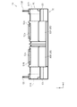
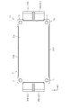
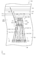
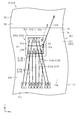
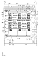
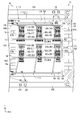
- the plan view of the power module of FIG. A side view of the power module of FIG. A side view of the power module of FIG. 1 as viewed from a direction different from that of FIG.
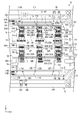
- the bottom view of the power module of FIG. The plan view which shows the internal structure of the power module of FIG.
- the circuit diagram which shows the circuit structure of the power module of FIG. An enlarged view of a part of FIG. 7. An enlarged view of a part of FIG. 7. An enlarged view of a part of FIG. 7.
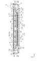
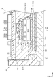
- FIG. 7 is a cross-sectional view taken along the line 12-12 of FIG.
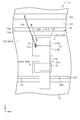
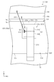
- FIG. 7 is a cross-sectional view taken along the line 15-15 of FIG. An enlarged view of a part of FIG. An enlarged view of a part of FIG. Enlarged view of the second power semiconductor element, the second diode, and their surroundings.
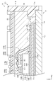
- FIG. 7 is a cross-sectional view taken along the line 19-19 of FIG. An enlarged view of a part of FIG.
- FIG. 7 is a cross-sectional view taken along the line 21-21 of FIG.
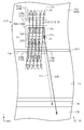
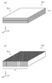
- FIG. 28 is a cross-sectional view taken along the line 29-29.
- FIG. 28 is a cross-sectional view taken along the line 30-30.
- An enlarged view of the second power semiconductor element and its surroundings for the power module of the modified example Top view of the first graphite plate and its surroundings for the power module of the modified example. Top view of the first graphite plate and its surroundings for the power module of the modified example. Top view of the first graphite plate and its surroundings for the power module of the modified example. Top view of the first graphite plate and its surroundings for the power module of the modified example.
- FIGS. 1 to 27 show the external shape of the power module 1A.
- FIG. 7 shows the internal structure of the power module 1A.
- the power module 1A includes a substrate 10, a connecting member 20, a power semiconductor element 30, a diode 40, a terminal 50, a sealing resin 60 (see FIG. 12), and heat dissipation which is an example of a cooler. It mainly includes a plate 70 and a case 80 for accommodating them. In FIG. 7, the sealing resin 60 is omitted for convenience. As shown in FIGS. 1 to 6, the substrate 10, the connecting member 20, the power semiconductor element 30, the diode 40, and the sealing resin 60 are housed by the heat radiating plate 70 and the case 80, respectively, and are not exposed to the outside.
- the terminal 50 is housed in the case 80 in a state where a part of the terminal 50 is exposed or protrudes to the outside of the case 80.
- the power module 1A is used, for example, in an inverter device.
- the shape of the power module 1A is rectangular when viewed from the thickness direction of the substrate 10 (hereinafter, referred to as “planar view”).
- the direction along the thickness direction of the substrate 10 is defined as the "thickness direction Z”
- the two directions orthogonal to the thickness direction Z are the "horizontal direction X" and the "vertical direction X", respectively.
- Direction Y In the present embodiment, the long side direction of the power module 1A is the horizontal direction X, and the short side direction is the vertical direction Y.
- FIG. 8 shows the circuit configuration of the power module 1A of this embodiment.
- the power module 1A includes a first power semiconductor element group 30AT composed of a plurality of first power semiconductor elements 30A as a power semiconductor element 30, a second power semiconductor element group 30BT composed of a plurality of second power semiconductor elements 30B, and a diode. It has a first diode group 40AT composed of a plurality of first diodes 40A as 40, and a second diode group 40BT composed of a plurality of second diodes 40B.
- FIG. 8 shows one first power semiconductor element 30A as the first power semiconductor element group 30AT, and one second power semiconductor element 30B as the second power semiconductor element group 30BT.
- Each of the first power semiconductor element 30A of the first power semiconductor element group 30AT and each second power semiconductor element 30B of the second power semiconductor element group 30BT are used as switching elements.
- Each of the power semiconductor elements 30A and 30B includes a transistor made of, for example, Si (silicon), SiC (silicon carbide), GaN (gallium nitride), GaAs (gallium arsenide), or Ga 2 O 3 (gallium oxide). It is used.
- Si silicon
- SiC silicon carbide
- GaN gallium nitride
- GaAs gallium arsenide
- Ga 2 O 3 gallium oxide
- Each of the power semiconductor elements 30A and 30B has a drain electrode 31, a source electrode 32, and a gate electrode 33. Further, each of the power semiconductor elements 30A and 30B has a body diode 34.
- the drain electrode 31 of the first power semiconductor element 30A is an example of the first back surface side drive electrode in the claims
- the drain electrode 31 of the second power semiconductor element 30B is an example of the second back surface side drive electrode.
- the source electrode 32 of the first power semiconductor element 30A is an example of a first main surface side drive electrode within the scope of claims
- the source electrode 32 of the second power semiconductor element 30B is an example of a second main surface side drive electrode.
- the gate electrode 33 of the first power semiconductor element 30A and the gate electrode 33 of the second power semiconductor element 30B are examples of control electrodes within the scope of the claims.
- Each diode 40A and 40B has an anode electrode 41 and a cathode electrode 42.
- the first diode 40A of the first diode group 40AT is connected in antiparallel to each of the plurality of first power semiconductor elements 30A of the first power semiconductor element group 30AT.
- the cathode electrode 42 of the first diode 40A is connected to the drain electrode 31 of the first power semiconductor element 30A
- the anode electrode 41 of the first diode 40A is connected to the source electrode 32 of the first power semiconductor element 30A. It is connected.
- the second diode 40B of the second diode group 40BT is connected in antiparallel to each of the plurality of second power semiconductor elements 30B of the second power semiconductor element group 30BT.
- the drain electrode 31, source electrode 32, and gate electrode 33 of the plurality of first power semiconductor elements 30A of the first power semiconductor element group 30AT and the plurality of second power semiconductor elements 30B of the second power semiconductor element group 30BT are Each is connected to the terminal 50.
- the terminal 50 includes a first input terminal 51A, a second input terminal 51B, a first output terminal 52A, a second output terminal 52B, a first control terminal 53A, and a second. It has a control terminal 53B, a first detection terminal 54A, a second detection terminal 54B, a power supply current terminal 55, and a pair of temperature detection terminals 56.
- the pair of temperature detection terminals 56 are not shown in FIG. 8 for convenience because they are not electrically connected to the power semiconductor elements 30A and 30B.
- the first output terminal 52A and the second output terminal 52B are examples of output terminals within the scope of the claims.
- the first input terminal 51A is electrically connected to the drain electrode 31 of the first power semiconductor element group 30AT. That is, the first input terminal 51A is electrically connected to each of the drain electrodes 31 of the plurality of first power semiconductor elements 30A.
- the second input terminal 51B is electrically connected to the source electrode 32 of the second power semiconductor device group 30BT. That is, the second input terminal 51B is electrically connected to each of the source electrodes 32 of the plurality of second power semiconductor elements 30B.
- the output terminals 52A and 52B are electrically connected to the node N1 between the source electrode 32 of the first power semiconductor device group 30AT and the drain electrode 31 of the second power semiconductor device group 30BT.
- the output terminals 52A and 52B are electrically connected to the node N1 between the source electrodes 32 of the plurality of first power semiconductor elements 30A and the drain electrodes 31 of the plurality of second power semiconductor elements 30B.
- the first control terminal 53A is electrically connected to the gate electrode 33 of the first power semiconductor device group 30AT. That is, the first control terminal 53A is electrically connected to each of the gate electrodes 33 of the plurality of first power semiconductor elements 30A.
- the second control terminal 53B is electrically connected to the gate electrode 33 of the second power semiconductor device group 30BT. That is, the second control terminal 53B is electrically connected to each of the gate electrodes 33 of the plurality of second power semiconductor elements 30B.
- the first detection terminal 54A is electrically connected to the source electrode 32 of the first power semiconductor device group 30AT. That is, the first detection terminal 54A is electrically connected to each of the source electrodes 32 of the plurality of first power semiconductor elements 30A.
- the second detection terminal 54B is electrically connected to the source electrode 32 of the second power semiconductor device group 30BT. That is, the second detection terminal 54B is electrically connected to each of the source electrodes 32 of the plurality of second power semiconductor elements 30B.
- the power supply current terminal 55 is electrically connected to the node N2 between the drain electrode 31 of the first power semiconductor element group 30AT and the first input terminal 51A.
- the power supply current terminal 55 is electrically connected to the node N2 between each of the drain electrodes 31 of the plurality of first power semiconductor elements 30A and the first input terminal 51A.
- the control terminals 53A and 53B, the detection terminals 54A and 54B, the power supply current terminal 55, and the pair of temperature detection terminals 56 are electrically connected to a control circuit (not shown) provided outside the power module 1A. Is connected.
- the terminals 51A, 51B, 52A, 52B, 53A, 53B, 54A, 54B, 55, 56 are provided in the case 80, respectively.
- the case 80 is formed in a frame shape surrounding the substrate 10, the connecting member 20, the power semiconductor element 30, and the diode 40 in a plan view.
- the case 80 is made of a synthetic resin having electrical insulation such as PPS (polyphenylene sulfide) and excellent heat resistance.
- the case 80 includes a pair of side walls 81A and 81B, a pair of terminal blocks 82A and 82B, a plurality of mounting portions 83, a power supply terminal block 84, and an output terminal block 85.
- the control terminals 53A and 53B, the detection terminals 54A and 54B, the power supply current terminal 55, and the pair of temperature detection terminals 56 are supported by the pair of side walls 81A and 81B, respectively. As shown in FIGS. 1 and 3, each control terminal 53A, 53B, each detection terminal 54A, 54B, a power supply current terminal 55, and a pair of temperature detection terminals 56 are a pair of side walls 81A, 81B in the thickness direction Z, respectively. Protruding from.
- the control terminals 53A and 53B, the detection terminals 54A and 54B, the power supply current terminal 55, and the pair of temperature detection terminals 56 are each made of, for example, a metal rod made of Cu (copper) as a constituent material.
- the surface of this metal rod is Sn (tin) plated. Nickel plating may be applied between the surface of the metal rod and the tin plating.
- the control terminals 53A and 53B, the detection terminals 54A and 54B, the power supply current terminal 55, and the pair of temperature detection terminals 56 all have the same shape, for example, and in one example, the first portion extending in the vertical direction Y and the thickness direction Z. It is formed in an L shape having a second portion extending to.
- the first input terminal 51A and the second input terminal 51B have the same shape as each other.
- the input terminals 51A and 51B have an exposed portion 51a exposed to the outside of the power module 1A, a connecting portion 51b for electrically connecting to the power semiconductor elements 30A and 30B, and an exposed portion 51a and a connecting portion 51b. It has a connecting portion 51c to be connected.
- each of the input terminals 51A and 51B is configured as a single component in which the exposed portion 51a, the connecting portion 51b, and the connecting portion 51c are integrally formed.
- the exposed portion 51a is provided with a through hole 51d that penetrates the exposed portion 51a in the thickness direction Z. As shown in FIG.
- the first input terminal 51A is formed in a stepped shape.
- the exposed portion 51a of the first input terminal 51A is supported by the first terminal block 84A.
- the exposed portion 51a of the second input terminal 51B is supported by the second terminal block 84B.
- the through hole 51d of the exposed portion 51a of the first input terminal 51A is provided corresponding to the nut 84N of the first terminal block 84A.
- the through hole 51d of the exposed portion 51a of the second input terminal 51B is provided corresponding to the nut 84N of the second terminal block 84B.
- a plurality of connecting portions 51b are provided and are arranged apart from each other in the vertical direction Y.
- the first output terminal 52A and the second output terminal 52B have the same shape.
- the output terminals 52A and 52B have the same shape as the input terminals 51A and 51B.
- the output terminals 52A and 52B have an exposed portion 52a exposed to the outside of the power module 1A, a connecting portion 52b for electrically connecting to the power semiconductor elements 30A and 30B, and an exposed portion 52a and a connecting portion 52b. It has a connecting portion 52c to be connected.
- the output terminals 52A and 52B are configured as a single component in which the exposed portion 52a, the connecting portion 52b, and the connecting portion 52c are integrally formed.
- the exposed portion 52a is provided with a through hole 52d that penetrates the exposed portion 52a in the thickness direction Z.
- the first output terminal 52A is formed in a stepped shape.
- the exposed portion 52a of the first output terminal 52A is supported by the first terminal block 85A.
- the exposed portion 52a of the second output terminal 52B is supported by the second terminal block 85B.
- the through hole 52d of the exposed portion 52a of the first output terminal 52A is provided corresponding to the nut 85N of the first terminal block 85A.
- the through hole 52d of the exposed portion 52a of the second output terminal 52B is provided corresponding to the nut 85N of the second terminal block 85B.
- a plurality of connecting portions 52b are provided and are arranged apart from each other in the vertical direction Y.
- the heat radiating plate 70 is attached to the case 80 to close one end of the opening opening in the thickness direction Z of the case 80.
- the heat radiating plate 70 is made of, for example, Al 2 O 3 (alumina).
- the heat radiating plate 70 may be made of a metal plate made of Cu. In this case, the surface of the metal plate may be nickel-plated.
- the heat radiating plate 70 has a heat radiating main surface 70s and a heat radiating back surface 70r facing opposite sides in the thickness direction Z. The heat radiating back surface 70r is exposed to the outside of the power module 1A.
- support holes 71 that penetrate the heat radiating plate 70 in the thickness direction Z are provided at the four corners of the heat radiating plate 70.
- a plurality of mounting portions 83 are provided at the four corners of the case 80 in a plan view.
- Each mounting portion 83 is provided with a mounting hole 83a that penetrates the mounting portion 83 in the thickness direction Z. Seen from the thickness direction Z, the plurality of mounting portions 83 are arranged so as to overlap the four corners of the heat radiating plate 70. Therefore, the plurality of mounting holes 83a correspond to the support holes 71 (see FIG. 6) of the heat radiating plate 70.
- the heat radiating plate 70 is supported by the case 80 by fitting a fastening member such as a pin into the plurality of mounting holes 83a and the support holes 71.
- the case 80 includes a top plate 86.
- the top plate 86 closes the internal region of the power module 1A formed by the heat radiating plate 70, the pair of side walls 81A and 81B, and the pair of terminal pedestals 82A and 82B.
- the top plate 86 is supported by a pair of side walls 81A and 81B in a state of being separated from the heat radiating plate 70 and the substrate 10 in the thickness direction Z.
- the sealing resin 60 is made of a resin material having electrical insulation, and is filled in an internal region closed by a heat radiating plate 70 and a top plate 86.
- the sealing resin 60 seals the substrate 10, the connecting member 20, the power semiconductor element 30, and the diode 40.
- the substrate 10 is joined to the heat dissipation main surface 70s of the heat dissipation plate 70 by a bonding material such as Ag (silver) paste or solder.
- the bonding material is not limited to the conductive bonding material such as Ag paste or solder, and an electrically insulating bonding material may be used.
- the substrate 10 has a first substrate 11 and a second substrate 12.
- the first substrate 11 and the second substrate 12 are arranged so as to be aligned in the vertical direction Y and separated in the horizontal direction X.
- the first substrate 11 is arranged on each input terminal 51A, 51B side of the internal region in the horizontal direction X
- the second substrate 12 is arranged on each output terminal 52A, 52B side of the internal region in the lateral direction X.
- the first substrate 11 has a first substrate main surface 11s and a first substrate back surface 11r facing opposite sides in the thickness direction Z.
- the second substrate 12 has a second substrate main surface 12s and a second substrate back surface 12r facing opposite sides in the thickness direction Z.
- the first substrate main surface 11s and the second substrate main surface 12s are examples of the substrate main surface within the scope of claims, and the first substrate back surface 11r and the second substrate back surface 12r are examples of the substrate back surface, respectively. is there.
- Each of the substrates 11 and 12 has a mounting layer for mounting the power semiconductor element 30 and the diode 40 on the substrates 11 and 12, and a conductive layer for electrically connecting the power semiconductor element 30 and the diode 40.
- the constituent materials of the substrates 11 and 12 are, for example, ceramics having excellent thermal conductivity. Examples of such ceramics include Al 2 O 3 (alumina), Al 2 O 3 containing ZrO (zirconium oxide), AlN (aluminum nitride), SiN (silicon nitride) and the like.
- the mechanical strength of the substrates 11 and 12 can be increased, and the substrates 11 and 12 can be manufactured at low cost.
- a resin material can be used as the constituent materials of the substrates 11 and 12.
- the resin material include epoxy resin, epoxy resin containing a reinforcing material such as glass cloth, and the like.
- DBC Direct Bonding Copper
- substrates 11 and 12 DBC (Direct Bonding Copper) substrates in which Cu (copper) foil is bonded to the main surfaces 11s and 12s of the substrates and the back surfaces 11r and 12r of the substrates can be used.
- the mounting layer, the conductive layer, and the like can be easily formed by patterning the copper foil bonded to the main surfaces 11s and 12s of each substrate. Further, the copper foil bonded to the back surfaces 11r and 12r of each substrate can be used as a heat transfer layer.
- the shape of the first substrate 11 in a plan view is a substantially rectangular shape in which the horizontal direction X is the long side direction and the vertical direction Y is the short side direction.
- the first substrate 11 mainly has a first substrate side surface 11a, a second substrate side surface 11b, a third substrate side surface 11c, and a fourth substrate side surface 11d.
- the first substrate side surface 11a and the second substrate side surface 11b are surfaces facing opposite to each other in the vertical direction Y, and extend along the horizontal direction X.
- the first substrate side surface 11a is the side surface of the first substrate 11 on the side wall 81A side
- the second substrate side surface 11b is the side surface of the first substrate 11 on the side wall 81B side.
- the third substrate side surface 11c and the fourth substrate side surface 11d are surfaces facing opposite to each other in the lateral direction X, and extend along the vertical direction Y.
- the third substrate side surface 11c is the side surface of the first substrate 11 on the terminal pedestal 82A side
- the fourth substrate side surface 11d is the side surface of the first substrate 11 on the terminal pedestal 82B (see FIG. 7) side.
- the first mounting layer 13A and the second mounting layer 13B which are examples of mounting layers, the conductive layer 14A, and an example of the control layer are used.
- a first control layer 15A and a second control layer 15B, a first detection layer 16A and a second detection layer 16B, and a thermistor mounting layer 17 are arranged.
- the first mounting layer 13A, the second mounting layer 13B, and the conductive layer 14A are arranged apart from each other in the vertical direction Y.
- the first mounting layer 13A is arranged on the side surface 11a of the first substrate 11 of the first substrate 11 with respect to the second mounting layer 13B and the conductive layer 14A in the vertical direction Y.
- the conductive layer 14A is arranged on the side surface 11b of the second substrate of the first substrate 11 with respect to the first mounting layer 13A and the second mounting layer 13B in the vertical direction Y.
- the second mounting layer 13B is arranged between the first mounting layer 13A and the conductive layer 14A in the vertical direction Y.
- the first mounting layer 13A is a connection formed between a band-shaped main mounting portion 13a extending in the lateral direction X and an end portion of the main mounting portion 13a in the lateral direction X on the third substrate side surface 11c side of the first substrate 11. It has a part 13b.
- the first mounting layer 13A is a single member in which the main mounting portion 13a and the connecting portion 13b are integrally formed.
- the connecting portion 13b extends in the vertical direction Y and protrudes from both sides of the main mounting portion 13a in the vertical direction Y.
- the connection portion 13b is arranged so as to be adjacent to the terminal pedestal 82A (see FIG. 7), that is, the first input terminal 51A in the lateral direction X.
- a plurality of connection portions 51b of the first input terminal 51A are connected to the connection portion 13b.
- the second mounting layer 13B is arranged on the side surface 11d of the fourth substrate of the first substrate 11 with respect to the connecting portion 13b of the first mounting layer 13A and the connecting portion 14b of the conductive layer 14A in the lateral direction X.
- the shape of the second mounting layer 13B in a plan view is a band shape extending in the lateral direction X.
- the second mounting layer 13B is arranged between the main mounting portion 13a of the first mounting layer 13A and the main conductive portion 14a of the conductive layer 14A in the vertical direction Y. In the present embodiment, the second mounting layer 13B is arranged closer to the side surface 11b of the second substrate of the first substrate 11 in the vertical direction Y.
- the second mounting layer 13B is located on the side surface 11b side of the second substrate with respect to the center line CLX whose central portion in the vertical direction Y extends from the central portion in the vertical direction Y of the first substrate 11 in the horizontal direction X. It is arranged like this.
- the edge of the second mounting layer 13B on the side surface 11d side of the fourth substrate in the lateral direction X and the side surface 11d side of the fourth substrate of the main mounting portion 13a of the first mounting layer 13A in the lateral direction X The edge and the edge of the main conductive portion 14a of the conductive layer 14A in the horizontal direction X on the side surface 11d of the fourth substrate are aligned in the vertical direction Y.
- the width dimension of the second mounting layer 13B (the dimension of the second mounting layer 13B in the vertical direction Y) is the width dimension of the main mounting portion 13a of the first mounting layer 13A (the dimension of the main mounting portion 13a in the vertical direction Y) and the conductivity. It is larger than the width dimension of the main conductive portion 14a of the layer 14A (the dimension of the main conductive portion 14a in the vertical direction Y).
- the first detection layer 16A is arranged closer to the main mounting portion 13a of the first mounting layer 13A than the first control layer 15A.
- the first control layer 15A is arranged on the side surface 11a of the first substrate of the first substrate 11 with respect to the first detection layer 16A. Seen from the vertical direction Y, the first control layer 15A overlaps with the first detection layer 16A.
- the length of the first detection layer 16A in the lateral direction X is longer than the length of the first control layer 15A in the lateral direction X.
- the side edges are aligned in the vertical direction Y.
- the end of the first detection layer 16A on the side surface 11c side of the third substrate of the first substrate 11 in the lateral direction X is from the end of the first control layer 15A on the side surface 11c of the third substrate in the lateral direction X. Is also located on the side surface 11c side of the third substrate.
- the second control layer 15B and the second detection layer 16B are respectively arranged on the second substrate side surface 11b side of the first substrate 11 with respect to the main conductive portion 14a of the conductive layer 14A in the vertical direction Y. Further, the second control layer 15B and the second detection layer 16B are respectively arranged on the side surface 11d of the fourth substrate of the first substrate 11 with respect to the connecting portion 14b of the conductive layer 14A in the lateral direction X. As described above, in a plan view, the main mounting portion 13a of the first mounting layer 13A, the second mounting layer 13B, and the main conductive portion 14a of the conductive layer 14A are the first control layer 15A, the first detection layer 16A, and the second.
- the first control layer 15A and the first detection layer 16A, the second control layer 15B and the second detection layer 16B are the main mounting portion 13a and the second mounting layer 13B of the first mounting layer 13A.
- And are arranged on both sides of the main conductive portion 14a of the conductive layer 14A.
- the shapes of the second control layer 15B and the second detection layer 16B in a plan view are strips extending in the lateral direction X, respectively.
- the second control layer 15B and the second detection layer 16B are arranged apart from each other in the vertical direction Y.
- the second detection layer 16B is arranged closer to the main conductive portion 14a of the conductive layer 14A than the second control layer 15B.
- the second control layer 15B is arranged on the side surface 11b of the second substrate of the first substrate 11 with respect to the second detection layer 16B.
- the second detection layer 16B overlaps with the second control layer 15B.
- the second detection layer 16B overlaps with the main conductive portion 14a of the conductive layer 14A.
- the side edges are aligned in the vertical direction Y. Further, the end of the first substrate 11 on the side surface 11d of the fourth substrate in the lateral direction X of the second detection layer 16B and the fourth substrate of the first substrate 11 in the lateral direction X of the second control layer 15B. The end portion on the side surface 11d side is aligned in the vertical direction Y.
- the length of the second control layer 15B in the lateral direction X is equal to the length of the second detection layer 16B in the lateral direction X.
- the length of each of the second control layer 15B and the second detection layer 16B in the lateral direction X is longer than the length of each of the first control layer 15A and the first detection layer 16A in the lateral direction X.
- the thermistor mounting layer 17 is arranged on the side surface 11a of the first substrate of the first substrate 11 with respect to the main mounting portion 13a of the first mounting layer 13A in the vertical direction Y. Further, the thermistor mounting layer 17 is arranged so as to overlap the connecting portion 13b of the first mounting layer 13A, the first control layer 15A, and the first detection layer 16A when viewed from the lateral direction X. Further, the thermistor mounting layer 17 is arranged between the first control layer 15A and the first detection layer 16A and the connecting portion 13b of the first mounting layer 13A in the lateral direction X.
- the thermistor 18 which is a temperature detection element can be mounted on the thermistor mounting layer 17.
- the thermistor 18 is mounted on the thermistor mounting layer 17.
- the thermistor mounting layer 17 has a pair of regions separated from each other in the lateral direction X.
- the positive electrode of the thermistor 18 can be electrically connected to one region, and the negative electrode of the thermistor 18 can be electrically connected to the other region.
- the shape of the second substrate 12 in a plan view is a substantially rectangular shape in which the horizontal direction X is the long side direction and the vertical direction Y is the short side direction.
- the shape of the second substrate 12 is a symmetrical shape centered on the center line along the vertical direction Y with respect to the first substrate 11, and the horizontal direction X, the vertical direction Y, and the thickness of the second substrate 12
- the size of the vertical direction Z is equal to the size of the first substrate 11 in the horizontal direction X, the vertical direction Y, and the thickness direction Z.
- the second substrate 12 mainly has a first substrate side surface 12a, a second substrate side surface 12b, a third substrate side surface 12c, and a fourth substrate side surface 12d.
- the first substrate side surface 12a and the second substrate side surface 12b are surfaces facing opposite to each other in the vertical direction Y, and extend along the horizontal direction X.
- the first substrate side surface 12a is the side surface of the second substrate 12 on the side wall 81A side
- the second substrate side surface 12b is the side surface of the second substrate 12 on the side wall 81B side.
- the third substrate side surface 12c and the fourth substrate side surface 12d are surfaces facing opposite sides in the lateral direction X, and extend along the vertical direction Y.
- the third substrate side surface 12c is the side surface of the second substrate 12 on the terminal pedestal 82A (see FIG. 7) side
- the fourth substrate side surface 12d is the terminal pedestal 82B (see FIG. 7) side of the second substrate 12. It is a side.
- the shape of the second substrate 12 does not have to be symmetrical with that of the first substrate 11, and the size of the second substrate 12 may be different from the size of the first substrate 11.
- the first mounting layer 13C and the second mounting layer 13D which are examples of mounting layers, the conductive layer 14B, and an example of the control layer are used.
- a first control layer 15C and a second control layer 15D, and a first detection layer 16C and a second detection layer 16D are arranged.
- the first mounting layer 13C, the second mounting layer 13D, and the conductive layer 14B are arranged apart from each other in the vertical direction Y.
- the first mounting layer 13C is arranged on the side surface 12a of the first substrate of the second substrate 12 with respect to the second mounting layer 13D and the conductive layer 14B in the vertical direction Y.
- the conductive layer 14B is arranged on the side surface 12b of the second substrate of the second substrate 12 with respect to the first mounting layer 13C and the second mounting layer 13D in the vertical direction Y.
- the second mounting layer 13D is arranged between the first mounting layer 13C and the conductive layer 14B in the vertical direction Y.
- the first mounting layer 13C is a connection formed between a strip-shaped main mounting portion 13c extending in the lateral direction X and an end portion of the main mounting portion 13c in the lateral direction X on the side surface 12d of the fourth substrate of the second substrate 12. It has a part 13d.
- the first mounting layer 13C is a single member in which the main mounting portion 13c and the connecting portion 13d are integrally formed.
- the connecting portion 13d extends in the vertical direction Y, and protrudes from the main mounting portion 13c toward the first substrate side surface 12a side of the second substrate 12 in the vertical direction Y.
- the shape of the first mounting layer 13C in a plan view is L-shaped.
- the shape of the conductive layer 14B in a plan view is a band shape extending in the lateral direction X.
- the width dimension of the conductive layer 14B (the dimension of the conductive layer 14B in the vertical direction Y) is smaller than the width dimension of the main mounting portion 13c of the first mounting layer 13C (the dimension of the main mounting portion 13c in the vertical direction Y).
- the second mounting layer 13D is a connection formed between a strip-shaped main mounting portion 13e extending in the lateral direction X and an end portion of the main mounting portion 13e in the lateral direction X on the side surface 11d of the fourth substrate of the first substrate 11. It has a portion 13f.
- the second mounting layer 13D is a single member in which the main mounting portion 13e and the connecting portion 13f are integrally formed.
- the main mounting portion 13e is arranged between the main mounting portion 13c of the first mounting layer 13C and the conductive layer 14B in the vertical direction Y. In the present embodiment, the main mounting portion 13e is arranged closer to the side surface 12b of the second substrate of the second substrate 12 in the vertical direction Y.
- the connecting portion 13f extends in the vertical direction Y and protrudes from both sides of the main mounting portion 13e in the vertical direction Y. As described above, the shape of the second mounting layer 13D in a plan view is T-shaped. Further, the connecting portion 13f is arranged on the side surface 12d of the fourth substrate of the second substrate 12 with respect to the first mounting layer 13C and the conductive layer 14B. The connection portion 13f is arranged so as to be adjacent to the terminal pedestal 82B, that is, the first output terminal 52A and the second output terminal 52B in the lateral direction X. A plurality of connection portions 52b of the output terminals 52A and 52B are connected to the connection portion 13f.
- the first control layer 15C and the first detection layer 16C are respectively arranged on the side surface 12a of the first substrate of the second substrate 12 with respect to the main mounting portion 13c of the first mounting layer 13C in the vertical direction Y. Further, the first control layer 15C and the first detection layer 16C are arranged on the third substrate side surface 12c side of the second substrate 12 with respect to the connection portion 13d of the first mounting layer 13C in the lateral direction X, respectively.
- the shapes of the first control layer 15C and the first detection layer 16C in a plan view are strips extending in the lateral direction X, respectively.
- the first control layer 15C and the first detection layer 16C are arranged apart from each other in the vertical direction Y.
- the first detection layer 16C is arranged closer to the main mounting portion 13c of the first mounting layer 13C than the first control layer 15C.
- the first control layer 15C is arranged on the side surface 12a of the first substrate of the second substrate 12 with respect to the first detection layer 16C.
- the first detection layer 16C overlaps with the first control layer 15C.
- the first detection layer 16C overlaps with the main mounting portion 13c of the first mounting layer 13C.
- the first control layer 15C and the first detection layer 16C overlap with the connection portion 13d of the first mounting layer 13C and the connecting portion 13f of the second mounting layer 13D, respectively.
- the length of the first control layer 15C in the lateral direction X is equal to the length of the first detection layer 16C in the lateral direction X.
- the side edges are aligned in the vertical direction Y.
- the end portion on the side surface 12d side is aligned in the vertical direction Y.
- the second control layer 15D and the second detection layer 16D are respectively arranged on the second substrate side surface 12b side of the second substrate 12 with respect to the conductive layer 14B in the vertical direction Y. Further, the second control layer 15D and the second detection layer 16D are arranged on the third substrate side surface 12c side of the second substrate 12 with respect to the connection portion 13f of the second mounting layer 13D in the lateral direction X, respectively.
- the main mounting portion 13c of the first mounting layer 13C, the main mounting portion 13e of the second mounting layer 13D, and the conductive layer 14B are the first control layer 15C, the first detection layer 16C, and the second. It is sandwiched in the vertical direction Y by the control layer 15D and the second detection layer 16D.
- the first control layer 15C and the first detection layer 16C and the second control layer 15D and the second detection layer 16D are the main mounting portion 13c and the second mounting layer 13D of the first mounting layer 13C. It is arranged on both sides of the main mounting portion 13e and the conductive layer 14B.
- the shapes of the second control layer 15D and the second detection layer 16D in a plan view are strips extending in the lateral direction X, respectively.
- the second control layer 15D and the second detection layer 16D are arranged apart from each other in the vertical direction Y.
- the second detection layer 16D is arranged closer to the conductive layer 14B than the second control layer 15D.
- the second control layer 15D is arranged on the side surface 12b side of the second substrate of the second substrate 12 with respect to the second detection layer 16D. Seen from the vertical direction Y, the second detection layer 16D overlaps with the second control layer 15D. Seen from the vertical direction Y, the second control layer 15D overlaps with the conductive layer 14B. The end of the second detection layer 16D on the third substrate side surface 12c side in the lateral direction X and the third substrate side surface 12c of the second substrate 12 in the lateral direction X of the second control layer 15D. The side edges are aligned in the vertical direction Y.
- the end portion on the side surface 12d side is aligned in the vertical direction Y.
- the length of the second control layer 15D in the lateral direction X is equal to the length of the second detection layer 16D in the lateral direction X.
- the length of each of the second control layer 15D and the second detection layer 16D in the lateral direction X is longer than the length of each of the first control layer 15C and the first detection layer 16C in the lateral direction X.
- the main mounting portion 13a of the first mounting layer 13A and the main mounting portion 13c of the first mounting layer 13C are arranged apart from each other in the horizontal direction X in a state of being aligned in the vertical direction Y.
- the second mounting layer 13B and the main mounting portion 13e of the second mounting layer 13D are arranged apart from each other in the horizontal direction X in a state of being aligned in the vertical direction Y.
- the main conductive portion 14a of the conductive layer 14A and the conductive layer 14B are arranged apart from each other in the horizontal direction X in a state of being aligned in the vertical direction Y.
- the main mounting portion 13a of the first mounting layer 13A and the main mounting portion 13c of the first mounting layer 13C are connected by a plate-shaped connecting member 100A.
- the second mounting layer 13B and the main mounting portion 13e of the second mounting layer 13D are connected by a plate-shaped connecting member 100B.
- the main conductive portion 14a of the conductive layer 14A and the conductive layer 14B are connected by a plate-shaped connecting member 100C.
- the connecting member 100A is an example of a first connecting member within the scope of claims
- the connecting member 100B is an example of a second connecting member
- the connecting member 100C is an example of a third connecting member.
- the shapes of the connecting members 100A to 100C are the same as each other in a plan view.
- the connecting members 100A to 100C are each made of Cu or a Cu alloy.
- Each of the connecting members 100A to 100C has a pair of connecting portions 101 extending in the horizontal direction X and a connecting portion 102 connecting the pair of connecting portions 101 in the vertical direction Y.
- each of the connecting members 100A to 100C is configured as a single member in which a pair of connecting portions 101 and a connecting portion 102 are integrally formed.
- the pair of connecting portions 101 are separated from each other in the vertical direction Y, and each extends in the horizontal direction X.
- the connecting portion 102 is provided so as to connect the central portions of the pair of connecting portions 101 in the lateral direction X to each other. Therefore, the shapes of the connecting members 100A to 100C in a plan view are H-shaped, respectively.
- the pair of connecting portions 101 of the connecting member 100A is an end portion of the main mounting portion 13a of the first mounting layer 13A on the side surface 11d side of the fourth substrate (side of the first mounting layer 13C) of the first substrate 11 in the lateral direction X. And the end of the main mounting portion 13c of the first mounting layer 13C on the side surface 12c side of the third substrate (side of the first mounting layer 13A) of the second substrate 12 in the lateral direction X.
- the connecting portion 102 of the connecting member 100A is located between the main mounting portion 13a and the main mounting portion 13c in the lateral direction X. In this way, the first mounting layer 13A and the first mounting layer 13C are electrically connected by the connecting member 100A.
- the pair of connecting portions 101 of the connecting member 100B are end portions on the side surface 11d side of the fourth substrate (side of the second mounting layer 13D) of the first substrate 11 in the lateral direction X of the second mounting layer 13B, and the second mounting portion 101. It is connected to the end of the second substrate 12 on the side surface 12c side (second mounting layer 13B side) of the second substrate 12 in the lateral direction X of the main mounting portion 13e of the layer 13D.
- the connecting portion 102 of the connecting member 100B is located between the second mounting layer 13B and the main mounting portion 13e in the lateral direction X. In this way, the second mounting layer 13B and the second mounting layer 13D are electrically connected by the connecting member 100B.
- the pair of connecting portions 101 of the connecting member 100C are the end portion of the main conductive portion 14a of the conductive layer 14A on the fourth substrate side surface 11d side (conductive layer 14B side) of the first substrate 11 in the lateral direction X, and the conductive layer. It is connected to the end of the second substrate 12 on the side surface 12c side (conductive layer 14A side) of the second substrate 12 in the lateral direction X of 14B.
- the connecting portion 102 of the connecting member 100C is located between the main conductive portion 14a and the conductive layer 14B in the lateral direction X. In this way, the conductive layer 14A and the conductive layer 14B are electrically connected by the connecting member 100C.
- the first control layer 15A and the first control layer 15C are arranged apart from each other in the horizontal direction X in a state of being aligned in the vertical direction Y.
- the first detection layer 16A and the first detection layer 16C are arranged apart from each other in the horizontal direction X in a state of being aligned in the vertical direction Y.
- the second control layer 15B and the second control layer 15D are arranged apart from each other in the horizontal direction X in a state of being aligned in the vertical direction Y.
- the second detection layer 16B and the second detection layer 16D are arranged apart from each other in the horizontal direction X in a state of being aligned in the vertical direction Y.
- the first control layer 15A and the first control layer 15C are connected by the first control layer connecting member 103A.
- the first detection layer 16A and the first detection layer 16C are connected by a first detection layer connecting member 104A.
- the second control layer 15B and the second control layer 15D are connected by a second control layer connecting member 103B.
- the second detection layer 16B and the second detection layer 16D are connected by a second detection layer connecting member 104B.
- the control layer connecting members 103A and 103B and the detection layer connecting members 104A and 104B are, for example, wires formed by wire bonding, respectively.
- the first control layer connecting member 103A is composed of a plurality of wires, and is on the fourth substrate side surface 11d side (first control layer 15C side) of the first substrate 11 of the first control layer 15A in the lateral direction X. Is connected to the end of the first control layer 15C in the lateral direction X on the side surface 12c side of the third substrate (side of the first control layer 15A) of the second substrate 12. In this way, the first control layer 15A and the first control layer 15C are electrically connected by the first control layer connecting member 103A.
- the first detection layer connecting member 104A is composed of a plurality of wires, and is on the fourth substrate side surface 11d side (first detection layer 16C side) of the first substrate 11 of the first detection layers 16A in the lateral direction X. Is connected to the end of the first detection layer 16C in the lateral direction X on the side surface 12c side of the third substrate (side of the first detection layer 16A) of the second substrate 12. In this way, the first detection layer 16A and the first detection layer 16C are electrically connected by the first detection layer connecting member 104A.
- the second control layer connecting member 103B is composed of a plurality of wires, and is on the fourth board side surface 11d side (second control layer 15D side) of the first board 11 of the second control layer 15B in the lateral direction X. Is connected to the end of the second control layer 15D in the lateral direction X on the side surface 12c (second control layer 15B side) side of the second substrate 12. In this way, the second control layer 15B and the second control layer 15D are electrically connected by the second control layer connecting member 103B.
- the second detection layer connecting member 104B is composed of a plurality of wires, and is the fourth substrate side surface 11d side (second detection layer 16D side) of the first substrate 11 of the second detection layer 16B in the lateral direction X. Is connected to the end of the second detection layer 16D in the lateral direction X on the side surface 12c side of the third substrate (side of the second detection layer 16B). In this way, the second detection layer 16B and the second detection layer 16D are electrically connected by the second detection layer connecting member 104B.
- the side wall 81A of the case 80 is provided so as to be adjacent to the first control layers 15A and 15C and the thermistor mounting layer 17 in the vertical direction Y. Therefore, the first control terminal 53A, the first detection terminal 54A, the power supply current terminal 55, and the pair of temperature detection terminals 56 provided on the side wall 81A are equipped with the first control layers 15A and 15C and the thermistor in the vertical direction Y, respectively. It is arranged so as to be adjacent to the layer 17.
- the first control terminal 53A and the first detection terminal 54A are arranged on the second substrate 12 side of the first control layer 15A, and the first control is performed in the vertical direction Y. It is arranged so as to be adjacent to the layer 15C.
- the first control terminal 53A and the first detection terminal 54A are arranged so as to be adjacent to each other in the lateral direction X.
- the first control terminal 53A and the first detection terminal 54A are arranged closer to the third substrate side surface 12c of the second substrate 12 in the lateral direction X. In the lateral direction X, the first detection terminal 54A is arranged closer to the terminal pedestal 82B (see FIG. 7) than the first control terminal 53A.
- the power supply current terminal 55 is arranged on the terminal pedestal 82B side of the first control terminal 53A and the first detection terminal 54A in the lateral direction X.
- the power supply current terminal 55 is arranged so as to be adjacent to the connection portion 13d of the first mounting layer 13C in the vertical direction Y.
- the pair of temperature detection terminals 56 are arranged on the side surface 11c of the third substrate of the first substrate 11 with respect to the first control layer 15A.
- the pair of temperature detection terminals 56 are arranged so as to be adjacent to the thermistor mounting layer 17 in the vertical direction Y.
- the side wall 81B of the case 80 is arranged so as to be adjacent to the second control layers 15B and 15D in the vertical direction Y. Therefore, the second control terminal 53B and the second detection terminal 54B provided on the side wall 81B are arranged so as to be adjacent to the second control layers 15B and 15D in the vertical direction Y, respectively.
- the second control terminal 53B and the second detection terminal 54B are arranged closer to the first substrate 11 than the second control layer 15D so as to be adjacent to the second control layer 15B in the vertical direction Y. Have been placed.
- the second control terminal 53B and the second detection terminal 54B are arranged so as to be adjacent to each other in the lateral direction X.
- the second control terminal 53B and the second detection terminal 54B are arranged closer to the side surface 11d of the fourth substrate of the first substrate 11 in the lateral direction X. In the lateral direction X, the second control terminal 53B is arranged closer to the second substrate 12 than the second detection terminal 54B.
- the connecting member 20 formed as a bonding wire As shown in FIGS. 9 to 11, as the connecting member 20 formed as a bonding wire, the first element connecting member 21A which is an example of the first connecting member and the second connecting member 20 which is an example of the second connecting member.
- the constituent materials of the connecting members 21A, 21B, 22A, 22B, 23A, 23B, 24, 25A, 25B, 26A, 26B, 27 are, for example, Al (aluminum).
- the constituent material of each connecting member 21A, 21B, 22A, 22B, 23A, 23B, 24, 25A, 25B, 26A, 26B, 27 may be, for example, Au (gold).
- the power supply current detection connection member 24, the control terminal connection members 25A and 25B, the detection terminal connection portions 26A and 26B, and the thermistor connection member 27 will be described, and the element connection members 21A and 21B will be described.
- the control connecting members 22A and 22B and the detection connecting members 23A and 23B will be described later.
- the power supply current detection connecting member 24 connects the connection portion 13d of the first mounting layer 13C on the second substrate 12 and the power supply current terminal 55.
- the first mounting layer 13C and the power supply current terminal 55 are electrically connected by the power supply current detection connecting member 24.
- the first control terminal connecting member 25A connects the first control layer 15A and the first control terminal 53A.
- the connection member 25A for the first control terminal is connected to a portion of the first control layer 15A near the side surface 11d of the fourth board of the first board 11.
- the first control layers 15A and 15C and the first control terminal 53A are electrically connected by the first control terminal connecting member 25A and the first control layer connecting member 103A.
- connection member 26A for the first detection terminal connects the first detection layer 16C and the first detection terminal 54A.
- the connection member 26A for the first detection terminal is connected to the portion of the first detection layer 16C on the side of the first substrate 11 with respect to the first detection terminal 54A in the lateral direction X.
- the first detection layers 16A and 16C and the first detection terminal 54A are electrically connected by the first detection terminal connecting member 26A and the first detection layer connecting member 104A.
- the thermistor connecting member 27 is composed of two wires, and connects the thermistor mounting layer 17 and the temperature detection terminal 56.
- One wire connects one region of the pair of regions of the thermistor mounting layer 17 and one of the pair of temperature detection terminals 56.
- the remaining one wire connects the other region of the pair of regions of the thermistor mounting layer 17 to the other of the pair of temperature detection terminals 56.
- the thermistor 18 and the temperature detection terminal 56 are electrically connected by the thermistor connecting member 27.
- the second detection terminal connecting member 26B connects the second detection layer 16B and the second detection terminal 54B.
- the connection member 26B for the second detection terminal is connected to the portion of the second detection layer 16B near the side surface 11d of the fourth substrate of the first substrate 11 in the lateral direction X.
- the second detection layers 16B and 16D and the second detection terminal 54B are electrically connected by the second detection terminal connecting member 26B and the second detection layer connecting member 104B.
- first power semiconductor elements 30A are electrically connected to the first substrate 11, and three first power semiconductor elements 30A are electrically connected to the second substrate 12. Is connected. That is, in the present embodiment, the upper arm of the inverter circuit (first power semiconductor element group 30AT in FIG. 8) is configured by the six first power semiconductor elements 30A.
- a first graphite plate 90A which is an example of a graphite plate, is arranged on the first substrate 11, and three first power semiconductor elements 30A are arranged on the first graphite plate 90A.
- a first graphite plate 90C which is an example of a graphite plate, is arranged on the second substrate 12, and three first power semiconductor elements 30A are arranged on the first graphite plate 90C.
- the graphite plates 90A and 90C and the first power semiconductor element 30A will be described in detail.
- the first graphite plate 90A is laminated on the main mounting portion 13a of the first mounting layer 13A.
- the first graphite plate 90A is bonded to the main mounting portion 13a by a conductive bonding material such as Ag paste or solder.
- a conductive bonding material such as Ag paste or solder.
- the shape of the first graphite plate 90A is a rectangular shape in which the horizontal direction X is the long side direction and the vertical direction Y is the short side direction.
- the dimension of the first graphite plate 90A in the vertical direction Y is smaller than the width dimension of the main mounting portion 13a (the dimension of the main mounting portion 13a in the vertical direction Y).
- the first graphite plate 90A has a first plate main surface 95A and a first plate back surface 96A facing opposite sides in the thickness direction Z.
- the first plate main surface 95A is an example of the plate main surface, and faces the same side as the first substrate main surface 11s of the first substrate 11 in the thickness direction Z.
- the back surface 96A of the first plate is an example of the back surface of the plate, and faces the same side as the back surface 11r of the first substrate of the first substrate 11 in the thickness direction Z.
- a conductive layer 97A on the main surface side is laminated on the main surface 95A of the first plate.
- a conductive layer 98A on the back surface side is laminated on the back surface 96A of the first plate.
- the back surface side conductive layer 98A is bonded to the main mounting portion 13a by the conductive bonding material.
- the main surface side conductive layer 97A is formed over the entire surface of the first plate main surface 95A.
- the back surface side conductive layer 98A is formed over the entire surface of the back surface 96A of the first plate.
- the main surface side conductive layer 97A may be partially formed on the first plate main surface 95A.
- the back surface side conductive layer 98A may be partially formed on the back surface side 96A of the first plate.
- the first graphite plate 90A has a first plate side surface 91A and a second plate side surface 92A facing opposite sides in the vertical direction Y, and a third plate side surface 93A and a third plate side surface facing the opposite side in the horizontal direction X. It has 4 plate side surfaces 94A.
- the first plate side surface 91A faces the same side as the first substrate side surface 11a of the first substrate 11, and the second plate side surface 92A faces the same side as the second substrate side surface 11b of the first substrate 11.
- the third plate side surface 93A faces the same side as the third substrate side surface 11c of the first substrate 11, and the fourth plate side surface 94A faces the same side as the fourth substrate side surface 11d of the first substrate 11.
- the first plate side surface 91A is the first substrate 11 with respect to the edge 13g of the first substrate 11 on the first substrate side surface 11a side in the vertical direction Y of the main mounting portion 13a of the first mounting layer 13A. It is located on the side surface 11b side of the second substrate, and is arranged so as to be adjacent to the edge 13g in the vertical direction Y.
- the second plate side surface 92A is the first substrate side surface 11a of the first substrate 11 with respect to the edge 13h of the first substrate 11 on the second substrate side surface 11b side in the vertical direction Y of the main mounting portion 13a. It is located on the side and is arranged so as to be adjacent to the edge 13h in the vertical direction Y.
- the dimension of the first graphite plate 90A in the vertical direction Y is slightly smaller than the width dimension of the main mounting portion 13a (the dimension of the main mounting portion 13a in the vertical direction Y).
- a plurality of (three in this embodiment) first power semiconductor elements 30A and a plurality of (three in this embodiment) first diodes 40A are arranged on the first plate main surface 95A of the first graphite plate 90A. There is. More specifically, the plurality of first power semiconductor elements 30A and the plurality of first diodes 40A are bonded to the main surface side conductive layer 97A by a conductive bonding material such as Ag paste or solder.
- the three first power semiconductor elements 30A will be referred to as the first power semiconductor elements 30Aa, 30Ab, 30Ac
- the three first diodes 40A will be referred to as the first diodes 40Aa, 40Ab, 40Ac. ..
- the first power semiconductor elements 30Aa, 30Ab, and 30Ac are arranged apart from each other in the horizontal direction X in a state of being aligned in the vertical direction Y.
- the first power semiconductor elements 30Aa, 30Ab, and 30Ac are arranged closer to the first plate side surface 91A of the first graphite plate 90A in the vertical direction Y, respectively.
- the first power semiconductor elements 30Aa, 30Ab, and 30Ac are the first plate side surfaces 91A of the first plate main surface 95A (main surface side conductive layer 97A) of the first graphite plate 90A in the vertical direction Y, respectively. It is located at the end of the side.
- the first power semiconductor element 30Aa is arranged closer to the side surface 93A of the third plate of the first graphite plate 90A in the lateral direction X.
- the first power semiconductor element 30Aa is attached to the end of the first plate main surface 95A (main surface side conductive layer 97A) of the first graphite plate 90A on the side surface 93A side of the third plate in the lateral direction X. Have been placed. More specifically, in a plan view, the first power semiconductor element 30Aa is arranged so as to be adjacent to the third plate side surface 93A in the lateral direction X.
- the first power semiconductor element 30Aa is arranged on the third substrate side surface 11c side of the first substrate 11 with respect to the first control layer 15A and the first detection layer 16A. Seen from the vertical direction Y, the first power semiconductor element 30Aa is arranged so as to overlap the pair of thermistor mounting layers 17.
- the first power semiconductor element 30Ab is arranged in the central portion of the first plate main surface 95A (main surface side conductive layer 97A) of the first graphite plate 90A in the lateral direction X.
- the first power semiconductor element 30Ac is arranged closer to the side surface 94A of the fourth plate of the first graphite plate 90A in the lateral direction X.
- the first power semiconductor element 30Ac is attached to the end of the first plate main surface 95A (main surface side conductive layer 97A) of the first graphite plate 90A on the side surface 94A side of the fourth plate in the lateral direction X. Have been placed. More specifically, in a plan view, the first power semiconductor element 30Ac is arranged so as to be adjacent to the fourth plate side surface 94A in the lateral direction X.
- the first diodes 40Aa, 40Ab, and 40Ac are arranged apart from each other in the horizontal direction X in a state of being aligned in the vertical direction Y.
- the first diodes 40Aa, 40Ab, and 40Ac are respectively arranged in the vertical direction Y closer to the side surface 92A of the second plate of the first graphite plate 90A.
- the first diodes 40Aa, 40Ab, and 40Ac are located on the side surface 92A of the second plate of the main surface 95A (conductive layer 97A on the main surface side) of the first graphite plate 90A in the vertical direction Y, respectively. It is placed at the end.
- the first diodes 40Aa, 40Ab, and 40Ac are respectively arranged so as to be adjacent to the second plate side surface 92A in the vertical direction Y.
- the first diodes 40Aa, 40Ab, and 40Ac are arranged on the opposite sides of the first control layer 15A and the first detection layer 16A in the vertical direction Y, respectively.
- the first diodes 40Aa, 40Ab, and 40Ac are respectively arranged near the second mounting layer 13B in the vertical direction Y.
- the first diode 40Aa is arranged so as to be aligned with the first power semiconductor element 30Aa in the horizontal direction X and separated from the first power semiconductor element 30Aa in the vertical direction Y.
- the first diode 40Ab is arranged so as to be aligned with the first power semiconductor element 30Ab in the horizontal direction X and separated from the first power semiconductor element 30Ab in the vertical direction Y.
- the first diode 40Ac is arranged so as to be aligned with the first power semiconductor element 30Ac in the horizontal direction X and separated from the first power semiconductor element 30Ac in the vertical direction Y.
- the first power semiconductor elements 30Aa, 30Ab, and 30Ac are arranged so as to have the same structure and the same orientation as each other. As shown in FIG. 13, the first power semiconductor elements 30Aa, 30Ab, and 30Ac each have an element main surface 30s and an element back surface 30r facing opposite sides in the thickness direction Z.
- the element main surface 30s of the first power semiconductor element 30A is an example of the first element main surface
- the element back surface 30r of the first power semiconductor element 30A is an example of the back surface of the first element.
- a source electrode 32 and a gate electrode 33 are formed on the element main surface 30s of the first power semiconductor element 30Ab.
- the source electrode 32 includes a first source electrode 32A and a second source electrode 32B.
- the first source electrode 32A and the second source electrode 32B are arranged apart from each other in the vertical direction Y.
- the first source electrode 32A is arranged on the side surface 91A of the first plate of the first graphite plate 90A with respect to the second source electrode 32B.
- the gate electrode 33 is arranged in the recess 32a formed in the source electrode 32.
- the source electrode 32 and the gate electrode 33 are formed on the element main surface 30s of the first power semiconductor elements 30Aa and 30Ac as well as the element main surface of the first power semiconductor element 30Ab. ing.
- the first diodes 40Aa, 40Ab, and 40Ac have the same structure as each other.
- the first diode 40Ab has a main surface 40s and a back surface 40r facing opposite sides in the thickness direction Z.
- the main surface 40s is a surface facing the same side as the element main surface 30s in the thickness direction Z
- the back surface 40r is a surface facing the same side as the device back surface 30r in the thickness direction Z.
- the main surface 40s is an example of the first main surface of the first diode described in the claims.
- the back surface 40r is an example of the first back surface of the first diode described in the claims.
- a cathode electrode 42 (not shown in FIG. 16) is formed on the back surface 40r of the first diode 40Ab.
- the cathode electrode 42 is formed over the entire back surface 40r, for example.
- the cathode electrode 42 is bonded to the main surface side conductive layer 97A laminated on the first plate main surface 95A of the first graphite plate 90A via a conductive bonding material.
- the cathode electrode 42 of the first diode 40Ab is electrically connected to the drain electrode 31 of the first power semiconductor elements 30Aa, 30Ab, 30Ac.
- the source electrode 32 of the first power semiconductor element 30Ab, the anode electrode 41 of the first diode 40Ab, and the second mounting layer 13B are connected by the first element connecting member 21A.
- the first element connecting member 21A includes a plurality of (five in the present embodiment) first element connecting member 21Aa and a plurality of (four in the present embodiment) first element connecting member 21Ab. ..
- the plurality of first element connecting members 21Aa connect the second source electrode 32B of the first power semiconductor element 30Ab, the anode electrode 41 of the first diode 40Ab, and the second mounting layer 13B, respectively.
- Each of the plurality of first element connecting members 21Ab connects the first source electrode 32A and the second mounting layer 13B of the first power semiconductor element 30Ab.
- the plurality of first element connecting members 21Aa are arranged and connected to the second source electrode 32B in the vertical direction Y while being aligned with each other in the horizontal direction X, and are connected to the anode electrode 41 in the vertical direction. They are arranged and connected to the second mounting layer 13B while being aligned with each other in the horizontal direction X, and are arranged and connected to the second mounting layer 13B while being aligned with each other in the vertical direction X. Has been done.
- the plurality of first element connecting members 21Aa connecting the second source electrode 32B, the anode electrode 41, and the second mounting layer 13B extend along the vertical direction Y.
- the plurality of first element connecting members 21Ab are connected to a region of the first source electrode 32A near the third plate side surface 93A (see FIG. 9) of the first graphite plate 90A in the lateral direction X.
- the plurality of first element connecting members 21Ab are arranged and connected to the first source electrode 32A so as to be spaced apart from each other in the horizontal direction X in a state of being aligned with each other in the vertical direction Y.
- the plurality of first element connecting members 21Ab are formed so as to straddle the plurality of first element connecting members 21Aa.
- the two first element connecting members 21Ab are the third substrate side surface 11c of the first substrate 11 rather than the plurality of first element connecting members 21Aa connected to the second mounting layer 13B of the second mounting layer 13B (FIG. 9)
- the side portion is connected to a plurality of first element connecting members 21Aa so as to be adjacent to each other in the lateral direction X.
- the remaining two first element connecting members 21Ab are the fourth substrate side surface 11d of the first substrate 11 more than the plurality of first element connecting members 21Aa connected to the second mounting layer 13B of the second mounting layer 13B.
- a plurality of first element connecting members 21Aa are connected to the portion on the side (see FIG. 9) so as to be adjacent to each other in the lateral direction X.
- the distance between the two first element connecting members 21Aa and the remaining two first element connecting members 21Aa in the lateral direction X is from the first source electrode 32A. 2 It is formed so as to gradually widen toward the mounting layer 13B.
- the gate electrode 33 of the first power semiconductor element 30Ab and the first control layer 15A are connected by a first control connecting member 22A.
- the first control connecting member 22A is connected to the vicinity of the central portion of the first control layer 15A in the lateral direction X. In this way, the gate electrode 33 is electrically connected to the first control terminal 53A (see FIG. 11) via the first control layers 15A and 15C by the first control connecting member 22A.
- the configuration in which the source electrode 32 of the first power semiconductor element 30Aa, the anode electrode 41 of the first diode 40Aa, and the second mounting layer 13B are connected by the first element connecting member 21A (21Aa, 21Ab) is the first.
- the gate electrode 33 of the first power semiconductor element 30Aa and the first control layer 15A are connected by the first control connecting member 22A, and the gate of the first power semiconductor element 30Ac is connected by the first control connecting member 22A.
- the configuration in which the electrode 33 and the first control layer 15A are connected is the same as the configuration in which the gate electrode 33 of the first power semiconductor element 30Ab and the first control layer 15A are connected by the first control connecting member 22A. ..
- the first control connecting member 22A connected to the gate electrode 33 of the first power semiconductor element 30Aa is the third substrate of the first substrate 11 of the first control layer 15A in the lateral direction X. It is connected to the end on the side surface 11c side.
- the first control connecting member 22A connected to the gate electrode 33 of the first power semiconductor element 30Ac is located at the end of the first control layer 15A on the side surface 11d of the fourth substrate in the lateral direction X. It is connected.
- the first control connecting member 22A connected to the gate electrode 33 of the first power semiconductor element 30Ac is the first control layer connecting member 103A of the first control layer 15A in the lateral direction X. It is connected to a portion between a portion connected to the first control layer 15A and a portion of the first control terminal connecting member 25A connected to the first control layer 15A.
- the source electrode 32 of the first power semiconductor element 30Aa and the first detection layer 16A are connected by the first detection connecting member 23A, and the source of the first power semiconductor element 30Ac is connected by the first detection connecting member 23A.
- the configuration in which the electrode 32 and the first detection layer 16A are connected is the same as the configuration in which the source electrode 32 of the first power semiconductor element 30Ab and the first detection layer 16A are connected by the first detection connecting member 23A. ..
- the first detection connecting member 23A connected to the source electrode 32 of the first power semiconductor element 30Aa is located at the end of the first detection layer 16A on the third substrate side surface 11c side of the first detection layer 16A in the lateral direction X. It is connected.
- the first detection connecting member 23A connected to the source electrode 32 of the first power semiconductor element 30Ac is connected to the portion of the first detection layer 16A on the side surface 11d of the fourth substrate 11 in the lateral direction X. Has been done.
- the first graphite plate 90C is laminated on the first mounting layer 13C of the second substrate 12.
- the first graphite plate 90C is bonded to the main mounting portion 13c of the first mounting layer 13C by a conductive bonding material such as Ag paste or solder.
- the shape of the first graphite plate 90C is a rectangular shape in which the horizontal direction X is the long side direction and the vertical direction Y is the short side direction.
- the dimension of the first graphite plate 90C in the vertical direction Y is smaller than the width dimension of the main mounting portion 13c (the dimension of the main mounting portion 13c in the vertical direction Y).
- the thickness dimension of the first graphite plate 90C (dimension in the thickness direction Z of the first graphite plate 90C) is larger than the thickness dimension of the second substrate 12 (dimension in the thickness direction Z of the second substrate 12).
- the size of the first graphite plate 90C is the same as the size of the first graphite plate 90A. More specifically, the dimension Y in the longitudinal direction of the first graphite plate 90C is equal to the dimension Y in the longitudinal direction of the first graphite plate 90A. Further, the dimension of the first graphite plate 90C in the lateral direction X is equal to the dimension of the first graphite plate 90A in the lateral direction X.
- the thickness dimension of the first graphite plate 90C (dimension in the thickness direction Z of the first graphite plate 90C) is the same as the thickness dimension of the first graphite plate 90A (dimension in the thickness direction Z of the first graphite plate 90A). equal.
- the difference between the vertical direction Y dimension of the first graphite plate 90C and the vertical direction Y dimension of the first graphite plate 90A is, for example, within 5% of the vertical direction Y dimension of the first graphite plate 90A. It can be said that the dimension Y in the vertical direction of the first graphite plate 90C is equal to the dimension Y in the vertical direction of the first graphite plate 90A.
- the first 1 It can be said that the dimension of the graphite plate 90C in the lateral direction X is equal to the dimension of the first graphite plate 90A in the lateral direction X. Further, the difference between the dimension of the first graphite plate 90C in the thickness direction Z and the dimension of the first graphite plate 90A in the thickness direction Z is, for example, within 5% of the dimension of the first graphite plate 90A in the thickness direction Z. For example, it can be said that the thickness dimension of the first graphite plate 90C is equal to the thickness dimension of the first graphite plate 90A.
- the first graphite plate 90C has a first plate main surface 95C and a first plate back surface 96C facing opposite sides in the thickness direction Z.
- the first plate main surface 95C faces the same side as the second substrate main surface 12s of the second substrate 12 in the thickness direction Z.
- the back surface 96C of the first plate faces the same side as the back surface 12r of the second substrate of the second substrate 12 in the thickness direction Z.
- a conductive layer 97C on the main surface side is laminated on the main surface 95C of the first plate.
- a conductive layer 98C on the back surface side is laminated on the back surface 96C of the first plate.
- the back surface side conductive layer 98C is bonded to the main mounting portion 13c by the conductive bonding material.
- the main surface side conductive layer 97C is formed over the entire surface of the first plate main surface 95C.
- the back surface side conductive layer 98C is formed over the entire surface of the back surface 96C of the first plate.
- the main surface side conductive layer 97C may be partially formed on the first plate main surface 95C.
- the back surface side conductive layer 98C may be partially formed on the back surface side 96C of the first plate.
- the first graphite plate 90C has a first plate side surface 91C and a second plate side surface 92C facing opposite sides in the vertical direction Y, and a third plate side surface 93C and a fourth plate side surface 94C facing opposite sides in the horizontal direction X. ..
- the first plate side surface 91C faces the same side as the first substrate side surface 12a of the second substrate 12, and the second plate side surface 92C faces the same side as the second substrate side surface 12b of the second substrate 12.
- the third plate side surface 93C faces the same side as the third substrate side surface 12c of the second substrate 12, and the fourth plate side surface 94C faces the same side as the fourth substrate side surface 12d of the second substrate 12.
- the first plate side surface 91C is the second substrate 12 with respect to the edge 13k of the second substrate 12 on the first substrate side surface 12a side in the vertical direction Y of the main mounting portion 13c of the first mounting layer 13C. It is located on the side surface 12b side of the second substrate, and is arranged so as to be adjacent to the edge 13k in the vertical direction Y.
- the second plate side surface 92C is the first substrate side surface 12a of the second substrate 12 with respect to the edge 13m on the second substrate side surface 12b side of the second substrate 12 in the vertical direction Y of the main mounting portion 13c. It is located on the side and is arranged so as to be adjacent to the edge 13 m in the vertical direction Y.
- the dimension of the first graphite plate 90C in the vertical direction Y is slightly smaller than the width dimension of the main mounting portion 13c (the dimension of the main mounting portion 13c in the vertical direction Y).
- the third plate side surface 93C is located at the end of the main mounting portion 13c of the first mounting layer 13C on the third board side surface 12c side of the second board 12 in the lateral direction X. Specifically, in a plan view, the third plate side surface 93C is located adjacent to the connecting member 100A connected to the main mounting portion 13c in the lateral direction X. In a plan view, the fourth plate side surface 94C is located at the end of the second substrate 12 on the fourth substrate side surface 12d side of the main mounting portion 13c. Seen from the vertical direction Y, the first graphite plate 90C overlaps with the connecting portion 13d of the first mounting layer 13C.
- the first graphite plate 90C is located in the lateral direction X as much as possible between the edge of the second substrate 12 on the side surface 12d side of the fourth substrate in the first mounting layer 13C and the connecting member 100A in the lateral direction X. It is provided so that the length of the
- a plurality of (three in this embodiment) first power semiconductor elements 30A and a plurality of (three in this embodiment) first diodes 40A are arranged on the first plate main surface 95C of the first graphite plate 90C. There is. More specifically, the plurality of first power semiconductor elements 30A and the plurality of first diodes 40A are main surface side conductive layers 97A laminated on the first plate main surface 95C by a conductive bonding material such as Ag paste or solder. It is joined to.
- the three first power semiconductor elements 30A will be referred to as the first power semiconductor elements 30Ad, 30Ae, 30Af, and the three first diodes 40A will be referred to as the first diodes 40Ad, 40Ae, 40Af. ..
- the first power semiconductor elements 30Ad, 30Ae, and 30Af are arranged apart from each other in the horizontal direction X in a state of being aligned in the vertical direction Y.
- the first power semiconductor elements 30Ad, 30Ae, and 30Af are arranged closer to the first plate side surface 91C of the first graphite plate 90C in the vertical direction Y, respectively.
- the first power semiconductor elements 30Ad, 30Ae, and 30Af are the first plate side surfaces 91C of the first plate main surface 95C (main surface side conductive layer 97C) of the first graphite plate 90C in the vertical direction Y, respectively. It is located at the end of the side.
- the first power semiconductor elements 30Ad, 30Ae, and 30Af are arranged so as to be adjacent to the first plate side surface 91C in the vertical direction Y, respectively. As described above, in the plan view, the first power semiconductor elements 30Ad, 30Ae, and 30Af are arranged near the first control layer 15C and the first detection layer 16C in the vertical direction Y, respectively.
- the first power semiconductor element 30Ad is arranged closer to the side surface 93C of the third plate of the first graphite plate 90C in the lateral direction X.
- the first power semiconductor element 30Ac is attached to the end of the first plate main surface 95C (main surface side conductive layer 97C) of the first graphite plate 90C on the side surface 93C side of the third plate in the lateral direction X. Have been placed. More specifically, in a plan view, the first power semiconductor element 30Ac is arranged so as to be adjacent to the third plate side surface 93C in the lateral direction X. When viewed from the vertical direction Y, the first power semiconductor element 30Ac is arranged so as to overlap the first control layer 15C and the first detection layer 16C.
- the first power semiconductor element 30Ae is arranged in the central portion of the first plate main surface 95C (main surface side conductive layer 97C) of the first graphite plate 90C in the lateral direction X.
- the first power semiconductor element 30Af is arranged closer to the side surface 94C of the fourth plate of the first graphite plate 90C in the lateral direction X.
- the first power semiconductor element 30Af is attached to the end of the first plate main surface 95C (main surface side conductive layer 97C) of the first graphite plate 90C on the side surface 94C side of the fourth plate in the lateral direction X. Have been placed.
- the first power semiconductor element 30Af is arranged so as to be adjacent to the fourth plate side surface 94C in the lateral direction X. Further, the first power semiconductor element 30Af is arranged on the side surface 12d of the fourth substrate of the second substrate 12 with respect to the first control layer 15C and the first detection layer 16C in the lateral direction X. Seen from the vertical direction Y, the first power semiconductor element 30Af overlaps with the connecting portion 13d of the first mounting layer 13C.
- the distance DX9 between the first power semiconductor element 30Ad and the first power semiconductor element 30Ae in the lateral direction X is larger than the distance DX10 between the first power semiconductor element 30Ad and the connecting member 100A in the lateral direction X.
- the distance DX9 is more than twice the distance DX10.
- the distance DX9 is at least three times the distance DX10. More preferably, the distance DX9 is four times or more the distance DX10. In this embodiment, the distance DX9 is about 7.4 times the distance DX10.
- the first diodes 40Ad, 40Ae, and 40Af are arranged apart from each other in the horizontal direction X in a state of being aligned in the vertical direction Y.
- the first diodes 40Ad, 40Ae, and 40Af are respectively arranged in the vertical direction Y closer to the second plate side surface 92C of the first graphite plate 90C.
- the first diodes 40Ad, 40Ae, and 40Af are located on the side surface 92C side of the second plate of the main surface 95C (conducting layer 97C on the main surface side) of the first graphite plate 90C in the vertical direction Y, respectively. It is placed at the end.
- the first diodes 40Ad, 40Ae, and 40Af are respectively arranged so as to be adjacent to the second plate side surface 92C in the vertical direction Y.
- the first diodes 40Ad, 40Ae, and 40Af are arranged on the opposite sides of the first control layer 15C and the first detection layer 16C in the vertical direction Y, respectively.
- the first diodes 40Ad, 40Ae, and 40Af are respectively arranged near the second mounting layer 13D in the vertical direction Y.
- the first diode 40Ad is arranged apart from the first power semiconductor element 30Ad in the vertical direction Y while being aligned with the first power semiconductor element 30Ad in the horizontal direction X.
- the first diode 40Ae is arranged so as to be aligned with the first power semiconductor element 30Ae in the horizontal direction X and separated from the first power semiconductor element 30Ae in the vertical direction Y.
- the first diode 40Af is arranged so as to be aligned with the first power semiconductor element 30Af in the horizontal direction X and separated from the first power semiconductor element 30Af in the vertical direction Y.
- the first power semiconductor elements 30Ad, 30Ae, and 30Af are arranged so as to have the same structure and the same orientation as each other. Further, the first power semiconductor elements 30Ad, 30Ae and 30Af have the same structure as the first power semiconductor elements 30Aa, 30Ab and 30Ac. Therefore, the components of the first power semiconductor elements 30Ad, 30Ae, and 30Af are designated by the same reference numerals as the components of the first power semiconductor elements 30Aa, 30Ab, and 30Ac, and the description thereof will be omitted.
- the orientation of the first power semiconductor elements 30Ad, 30Ae, 30Af is different from the orientation of the first power semiconductor elements 30Aa, 30Ab, 30Ac.
- the first power semiconductor elements 30Aa, 30Ab, and 30Ac are oriented so that the gate electrode 33 is located on the side surface 11d side (terminal pedestal 82B side) of the fourth substrate of the first substrate 11, respectively (see FIG. 14).
- the first power semiconductor elements 30Ad, 30Ae, and 30Af are oriented so that the gate electrode 33 is located on the third substrate side surface 12c side (terminal pedestal 82A side) of the second substrate 12, respectively.
- the first diodes 40Ad, 40Ae, and 40Af have the same structure as each other. Further, the first diodes 40Ad, 40Ae, 40Af have the same structure as the first diodes 40Aa, 40Ab, 40Ac. Therefore, the components of the first diodes 40Ad, 40Ae, and 40Af are designated by the same reference numerals as the components of the first diodes 40Aa, 40Ab, and 40Ac, and the description thereof will be omitted.
- the first power semiconductor elements 30Ad, 30Ae, 30Af and the first diodes 40Ad, 40Ae, 40Af, the first element connecting member 21A, and the first control connection As shown in FIGS. 9, 10 and 18 to 20, the first power semiconductor elements 30Ad, 30Ae, 30Af and the first diodes 40Ad, 40Ae, 40Af, the first element connecting member 21A, and the first control connection.
- the connection relationship between the member 22A and the first detection connecting member 23A is, for example, the first power semiconductor element 30Ab and the first diode 40Ab, the first element connecting member 21A, the first control connecting member 22A, and the first detection.
- the connection relationship with the connection member 23A is the same.
- connection position of the gate electrodes 33 of the first power semiconductor elements 30Ad, 30Ae, 30Af of the first control connection member 22A in the lateral direction X and the connection position of the first control layer 15C is the first in the lateral direction X. 1
- the relationship between the connection position of the gate electrode 33 of the first power semiconductor elements 30Aa, 30Ab, 30Ac of the control connection member 22A and the connection position of the first control layer 15A is different.
- the connection position of the first control layer 15C of the first control connection member 22A is the first power semiconductor element 30Ae of the first control connection member 22A. It is located on the side surface 12c side of the third substrate of the second substrate 12 from the connection position of the gate electrode 33 of the above.
- connection position of the source electrodes 32 of the first power semiconductor elements 30Ad, 30Ae, and 30Af of the first detection connection member 23A in the lateral direction X and the connection position of the first detection layer 16C is the first in the lateral direction X. 1
- the relationship between the connection position of the source electrode 32 of the first power semiconductor elements 30Aa, 30Ab, 30Ac of the detection connection member 23A and the connection position of the first detection layer 16A is different.
- the connection position of the first detection layer 16C of the first detection connection member 23A is the first power semiconductor element 30Ae of the first detection connection member 23A. It is located on the side surface 12c side of the third substrate of the second substrate 12 from the connection position of the source electrode 32 of the above.
- the first detection connecting member 23A is connected to the region on the third substrate side surface 12c side of the second substrate 12 of the first source electrodes 32A of the first power semiconductor elements 30Ad, 30Ab, 30Ac. Has been done.
- the first detection connecting member 23A connected to the first source electrode 32A of the first power semiconductor element 30Ad is an end of the first detection layer 16C in the lateral direction X on the side surface 12c side of the third substrate 12. It is connected to the part. More specifically, the first detection connecting member 23A connected to the first source electrode 32A of the first power semiconductor element 30Ad is the connecting member 26A for the first detection terminal in the first detection layer 16C in the lateral direction X. It is connected to the portion between the portion connected to the first detection layer 16C and the portion of the first detection layer connecting member 104A connected to the first detection layer 16C.
- the first detection connecting member 23A connected to the first source electrode 32A of the first power semiconductor element 30Ae is connected to the central portion of the first detection layer 16C in the lateral direction X.
- the first detection connecting member 23A connected to the first source electrode 32A of the first power semiconductor element 30Af is an end of the first detection layer 16C on the side surface 12d of the fourth substrate of the first detection layer 16C in the lateral direction X. It is connected to the part.
- three second power semiconductor elements 30B are electrically connected to the first substrate 11, and three second power semiconductor elements 30B are electrically connected to the second substrate 12. Is connected. That is, in the present embodiment, the lower arm of the inverter circuit (second power semiconductor element group 30BT in FIG. 8) is configured by the six second power semiconductor elements 30B.
- a second graphite plate 90B which is an example of a graphite plate, is arranged on the first substrate 11, and three second power semiconductor elements 30B are arranged on the second graphite plate 90B.
- a second graphite plate 90D which is an example of a graphite plate, is arranged on the second substrate 12, and three second power semiconductor elements 30B are arranged on the second graphite plate 90D.
- the graphite plates 90B and 90D and the second power semiconductor element 30B will be described in detail.
- a second graphite plate 90B is laminated on the second mounting layer 13B.
- the second graphite plate 90B is bonded to the second mounting layer 13B by a conductive bonding material such as Ag paste or solder.
- the shape of the second graphite plate 90B is a rectangular shape in which the horizontal direction X is the long side direction and the vertical direction Y is the short side direction.
- the dimension of the second graphite plate 90B in the vertical direction Y is smaller than the width dimension of the second mounting layer 13B (the dimension of the second mounting layer 13B in the vertical direction Y).
- the thickness dimension of the second graphite plate 90B (dimension in the thickness direction Z of the second graphite plate 90B) is larger than the thickness dimension of the first substrate 11 (dimension in the thickness direction Z of the first substrate 11).
- the size of the second graphite plate 90B is the same as the size of the first graphite plate 90A. More specifically, the vertical Y dimension of the second graphite plate 90B is equal to the longitudinal Y dimension of the first graphite plate 90A. The lateral X dimension of the second graphite plate 90B is equal to the lateral X dimension of the first graphite plate 90A. The thickness dimension of the second graphite plate 90B (dimension in the thickness direction Z of the second graphite plate 90B) is the same as the thickness dimension of the first graphite plate 90A (dimension in the thickness direction Z of the first graphite plate 90A). equal.
- the difference between the vertical direction Y dimension of the second graphite plate 90B and the vertical direction Y dimension of the first graphite plate 90A is, for example, within 5% of the vertical direction Y dimension of the first graphite plate 90A. It can be said that the dimension Y in the vertical direction of the second graphite plate 90B is equal to the dimension Y in the vertical direction of the first graphite plate 90A.
- the first 2 It can be said that the dimension of the graphite plate 90B in the lateral direction X is equal to the dimension of the first graphite plate 90A in the lateral direction X. Further, the difference between the dimension of the second graphite plate 90B in the thickness direction Z and the dimension of the first graphite plate 90A in the thickness direction Z is, for example, within 5% of the dimension of the first graphite plate 90A in the thickness direction Z. For example, it can be said that the thickness dimension of the second graphite plate 90B is equal to the thickness dimension of the first graphite plate 90A.
- the second graphite plate 90B has a second plate main surface 95B and a second plate back surface 96B facing opposite sides in the thickness direction Z.
- the second plate main surface 95B is an example of the plate main surface, and faces the same side as the first substrate main surface 11s of the first substrate 11 in the thickness direction Z.
- the second plate back surface 96B is an example of the plate back surface, and faces the same side as the first substrate back surface 11r of the first substrate 11 in the thickness direction Z.
- a conductive layer 97B on the main surface side is laminated on the main surface 95B of the second plate.
- a conductive layer 98B on the back surface side is laminated on the back surface 96B of the second plate.
- the back surface side conductive layer 98B is bonded to the second mounting layer 13B by the conductive bonding material.
- the main surface side conductive layer 97B is formed over the entire surface of the second plate main surface 95B.
- the back surface side conductive layer 98B is formed over the entire surface of the back surface 96B of the second plate.
- the main surface side conductive layer 97B may be partially formed on the second plate main surface 95B.
- the back surface side conductive layer 98B may be partially formed on the back surface side 96B of the second plate.
- the second graphite plate 90B has a first plate side surface 91B and a second plate side surface 92B facing opposite sides in the vertical direction Y, and a third plate side surface 93B and a third plate side surface facing the opposite side in the horizontal direction X. It has 4 plate side surfaces 94B.
- the first plate side surface 91B faces the same side as the first substrate side surface 11a of the first substrate 11, and the second plate side surface 92B faces the same side as the second substrate side surface 11b of the first substrate 11.
- the third plate side surface 93B faces the same side as the third substrate side surface 11c of the first substrate 11, and the fourth plate side surface 94B faces the same side as the fourth substrate side surface 11d of the first substrate 11.
- the first plate side surface 91B is the second substrate side surface of the first substrate 11 with respect to the edge 13i of the first substrate 11 on the first substrate side surface 11a side in the vertical direction Y of the second mounting layer 13B. It is located on the 11b side and is arranged apart from the edge 13i in the vertical direction Y.
- the second plate side surface 92B is the first substrate side surface of the first substrate 11 with respect to the edge 13j on the second substrate side surface 11b side of the first substrate 11 in the vertical direction Y of the second mounting layer 13B. It is located on the 11a side and is arranged so as to be adjacent to the edge 13j in the vertical direction Y.
- the dimension of the second graphite plate 90B in the vertical direction Y is smaller than the width dimension of the second mounting layer 13B (the dimension of the main mounting portion 13a in the vertical direction Y). Further, the second graphite plate 90B is arranged closer to the second substrate side surface 11b of the first substrate 11 in the second mounting layer 13B in the vertical direction Y. As a result, a connection space between the first element connecting member 21A connected to the first power semiconductor element 30A and the first diode 40A in the second mounting layer 13B and the second mounting layer 13B is secured.
- the third plate side surface 93B is located at the end of the second mounting layer 13B on the third substrate side surface 11c side of the first substrate 11 in the lateral direction X.
- the fourth plate side surface 94B is located at the end of the second mounting layer 13B on the fourth substrate side surface 11d side of the first substrate 11.
- the fourth plate side surface 94B is located adjacent to the connecting member 100B connected to the second mounting layer 13B in the lateral direction X.
- the second graphite plate 90B is lateral as much as possible between the edge of the first substrate 11 on the side surface 11c side of the third substrate of the second mounting layer 13B and the connecting member 100B in the lateral direction X. It is provided so that the length of the direction X becomes long.
- a plurality of (three in this embodiment) second power semiconductor elements 30B and a plurality of (three in this embodiment) second diodes 40B are arranged on the second plate main surface 95B of the second graphite plate 90B.
- the plurality of second power semiconductor elements 30B and the plurality of second diodes 40B are main surface side conductive layers 97B laminated on the second plate main surface 95B by a conductive bonding material such as Ag paste or solder. It is joined to.
- the three second power semiconductor elements 30B will be referred to as the second power semiconductor elements 30Ba, 30Bb, 30Bc, and the three second diodes 40B will be referred to as the second diodes 40Ba, 40Bb, 40Bc. ..
- the second power semiconductor elements 30Ba, 30Bb, and 30Bc are arranged apart from each other in the horizontal direction X in a state of being aligned in the vertical direction Y.
- the second power semiconductor elements 30Ba, 30Bb, and 30Bc are arranged closer to the side surface 92B of the second plate of the second graphite plate 90B in the vertical direction Y, respectively.
- the second power semiconductor elements 30Ba, 30Bb, and 30Bc are the second plate side surfaces 92B of the second plate main surface 95B (main surface side conductive layer 97B) of the second graphite plate 90B in the vertical direction Y, respectively. It is located at the end of the side.
- the second power semiconductor elements 30Ba, 30Bb, and 30Bc are arranged so as to be adjacent to the second plate side surface 92B in the vertical direction Y, respectively. As described above, in the plan view, the second power semiconductor elements 30Ba, 30Bb, and 30Bc are respectively arranged near the conductive layer 14A in the vertical direction Y.
- the second power semiconductor element 30Ba is arranged closer to the side surface 93B of the third plate of the second graphite plate 90B in the lateral direction X.
- the second power semiconductor element 30Ba is attached to the end of the second plate main surface 95B (main surface side conductive layer 97B) of the second graphite plate 90B on the third plate side surface 93B side in the lateral direction X. Have been placed. More specifically, in a plan view, the second power semiconductor element 30Ba is arranged so as to be adjacent to the third plate side surface 93B in the lateral direction X.
- the second power semiconductor element 30Ba is arranged so as to overlap the second control layer 15B and the second detection layer 16B when viewed from the vertical direction Y.
- the second power semiconductor element 30Ba is arranged so as to overlap the first power semiconductor element 30Aa and the first diode 40Aa when viewed from the vertical direction Y. That is, the second power semiconductor element 30Ba is arranged apart from the first power semiconductor element 30Aa and the first diode 40Aa in the vertical direction Y while being aligned with the first power semiconductor element 30Aa and the first diode 40Aa in the horizontal direction X. Has been done.
- the second power semiconductor element 30Bb is arranged at the central portion of the second plate main surface 95B (main surface side conductive layer 97B) of the second graphite plate 90B in the lateral direction X. Further, the second power semiconductor element 30Bb is arranged so as to overlap the first power semiconductor element 30Ab and the first diode 40Ab when viewed from the vertical direction Y. That is, the second power semiconductor element 30Bb is arranged apart from the first power semiconductor element 30Ab and the first diode 40Ab in the vertical direction Y while being aligned with the first power semiconductor element 30Ab and the first diode 40Ab in the horizontal direction X. Has been done.
- the second power semiconductor element 30Bc is arranged closer to the side surface 94B of the fourth plate of the second graphite plate 90B in the lateral direction X.
- the second power semiconductor element 30Bc is attached to the end of the second plate main surface 95B (main surface side conductive layer 97B) of the second graphite plate 90B on the side surface 94B side of the fourth plate in the lateral direction X. Have been placed. More specifically, in a plan view, the second power semiconductor element 30Bc is arranged so as to be adjacent to the fourth plate side surface 94B in the lateral direction X.
- the second power semiconductor element 30Bc is arranged so as to overlap the first power semiconductor element 30Ac and the first diode 40Ac when viewed from the vertical direction Y. That is, the second power semiconductor element 30Bc is arranged apart from the first power semiconductor element 30Ac and the first diode 40Ac in the vertical direction Y while being aligned with the first power semiconductor element 30Ac and the first diode 40Ac in the horizontal direction X. Has been done.
- the distance DX5 between the second power semiconductor element 30Ba and the second power semiconductor element 30Bb in the lateral direction X is the distance between the second power semiconductor element 30Ba and the connection portion 51b of the second input terminal 51B in the lateral direction X. Larger than DX6. In one example, the distance DX5 is more than twice the distance DX6. Preferably, the distance DX5 is at least three times the distance DX6. More preferably, the distance DX5 is four times or more the distance DX6. In this embodiment, the distance DX5 is about 4.6 times the distance DX6.
- the distance DX7 between the second power semiconductor element 30Bc and the second power semiconductor element 30Bb in the lateral direction X is larger than the distance DX8 between the second power semiconductor element 30Bc and the connecting member 100B in the lateral direction X.
- the distance DX7 is more than twice the distance DX8.
- the distance DX7 is at least three times the distance DX8. More preferably, the distance DX7 is four times or more the distance DX8. In this embodiment, the distance DX7 is about 7.4 times the distance DX8.
- the distance DX7 is equal to the distance DX5.
- the difference between the distance DX7 and the distance DX5 is, for example, within 5% of the distance DX5, it can be said that the distance DX7 is equal to the distance DX5.
- the second diodes 40Ba, 40Bb, and 40Bc are arranged so as to be adjacent to the first plate side surface 91B in the vertical direction Y, respectively. More specifically, in the plan view, the second diodes 40Ba, 40Bb, and 40Bc are arranged so as to be adjacent to the first plate side surface 91B in the vertical direction Y, respectively. As described above, in the plan view, the second diodes 40Ba, 40Bb, and 40Bc are arranged on the opposite sides of the second control layer 15B and the second detection layer 16B in the vertical direction Y, respectively. The second diodes 40Ba, 40Bb, and 40Bc are respectively arranged near the first mounting layer 13A (first graphite plate 90A) in the vertical direction Y.
- the second diode 40Ba is arranged so as to be aligned with the second power semiconductor element 30Ba in the horizontal direction X and separated from the second power semiconductor element 30Ba in the vertical direction Y.
- the second diode 40Bb is arranged so as to be aligned with the second power semiconductor element 30Bb in the horizontal direction X and separated from the second power semiconductor element 30Bb in the vertical direction Y.
- the second diode 40Bc is arranged so as to be aligned with the second power semiconductor element 30Bc in the horizontal direction X and separated from the second power semiconductor element 30Bc in the vertical direction Y.
- the second power semiconductor elements 30Ba, 30Bb, and 30Bc are arranged so as to have the same structure and the same orientation as each other. That is, the element back surface 30r of the second power semiconductor elements 30Ba, 30Bb, 30Bc is joined to the main surface side conductive layer 97B of the second graphite plate 90B, and the element main surface 30s is the second graphite plate 90B in the thickness direction Z. It is located on the opposite side of.
- the second power semiconductor elements 30Ba, 30Bb, 30Bc have the same structure as the first power semiconductor elements 30Aa, 30Ab, 30Ac.
- the components of the second power semiconductor elements 30Ba, 30Bb, and 30Bc are designated by the same reference numerals as the components of the first power semiconductor elements 30Aa, 30Ab, and 30Ac, and the description thereof will be omitted.
- the element main surface of the second power semiconductor element 30B is an example of the second element main surface within the scope of claims, and the element back surface of the second power semiconductor element 30B is an example of the second element back surface.
- the second diodes 40Ba, 40Bb, 40Bc have the same structure as each other.
- the second diodes 40Ba, 40Bb, 40Bc have the same structure as the first diodes 40Aa, 40Ab, 40Ac. Therefore, the components of the second diodes 40Ba, 40Bb, 40Bc are designated by the same reference numerals as the components of the first diodes 40Aa, 40Ab, 40Ac, and the description thereof will be omitted.
- the second diode 40Ba, 40Bb, and 40Bc each have a main surface 40s and a back surface 40r, similarly to the first diode 40A.
- the main surface 40s is an example of the second main surface of the second diode described in the claims
- the back surface 40r is an example of the second back surface of the second diode described in the claims.
- the source electrode 32 of the second power semiconductor element 30Bb, the anode electrode 41 of the second diode 40Bb, and the conductive layer 14A are connected by the second element connecting member 21B.
- the second element connecting member 21B includes a plurality of (five in the present embodiment) second element connecting member 21Ba and a plurality of (four in the present embodiment) second element connecting member 21Bb. ..
- Each of the plurality of second element connecting members 21Ba connects the first source electrode 32A of the second power semiconductor element 30Bb, the anode electrode 41 of the second diode 40Bb, and the conductive layer 14A.
- Each of the plurality of second element connecting members 21Bb connects the second source electrode 32B of the second power semiconductor element 30Bb and the conductive layer 14A.
- the plurality of second element connecting members 21Bb are connected to a region of the second source electrode 32B near the third plate side surface 93B (see FIG. 9) of the second graphite plate 90B in the lateral direction X.
- the plurality of second element connecting members 21Bb are arranged and connected to the second source electrode 32B so as to be spaced apart from each other in the horizontal direction X in a state of being aligned with each other in the vertical direction Y.
- the plurality of second element connecting members 21Bb are arranged and connected to the conductive layer 14A so as to be spaced apart from each other in the horizontal direction X in a state of being aligned with each other in the vertical direction Y.
- Each of the plurality of second element connecting members 21Bb is arranged so as to be adjacent to the edge 14c on the side surface 11a (see FIG. 9) side of the first substrate 11 of the conductive layer 14A in the vertical direction Y. .. In a plan view, the plurality of second element connecting members 21Bb extend obliquely toward the third substrate side surface 11c (see FIG. 9) of the first substrate 11 as they move from the second source electrode 32B toward the conductive layer 14A. ..
- the plurality of second element connecting members 21Ba are arranged and connected to the second source electrode 32B in the vertical direction Y while being aligned with each other in the horizontal direction X, and are connected to the anode electrode 41 in the vertical direction. They are arranged and connected to the conductive layer 14A apart from each other in the horizontal direction X in a state of being aligned with each other in the Y direction, and are arranged and connected to the conductive layer 14A apart from each other in the horizontal direction X in a state of being aligned with each other in the vertical direction Y. There is. In a plan view, the portion of the plurality of second element connecting members 21Ba that connects the second source electrode 32B and the anode electrode 41 extends along the vertical direction Y.
- the portion of the plurality of second element connecting members 21Ba that connects the second source electrode 32B and the conductive layer 14A is the third portion of the first substrate 11 as it goes from the second source electrode 32B toward the conductive layer 14A. It extends diagonally toward the side surface 11c of the substrate.
- the portion of the plurality of second element connecting members 21Ba that connects the anode electrode 41 and the conductive layer 14A is formed so as to straddle the plurality of second element connecting members 21Bb. Therefore, the plurality of second element connecting members 21Ba are connected to the portion of the conductive layer 14A on the second substrate side surface 11b side of the plurality of second element connecting members 21Bb in the vertical direction Y. There is.
- the second element connecting member 21Ba is possible to prevent the second element connecting member 21Ba from overlapping the second control connecting member 22B and the second detection connecting member 23B in a plan view. Further, in a plan view, the second element connecting member 21Bb also extends diagonally like the second element connecting member 21Ba, so that the second element connecting member 21Bb and the second element connecting member 21Ba do not overlap with each other. ..
- the second power semiconductor element 30Bb and the second diode 40Bb are connected in antiparallel, and the drain electrode 31 of the second power semiconductor element 30Bb and the cathode electrode 42 of the second diode 40Bb are first. It is electrically connected to the source electrode 32 of the power semiconductor element 30Ab and the anode electrode 41 of the first diode 40Ab. Further, the source electrode 32 of the second power semiconductor element 30Bb and the anode electrode 41 of the second diode 40Bb are electrically connected to the second input terminal 51B.
- the second source electrode 32B and the second detection layer 16B of the second power semiconductor element 30Bb are connected by a second detection connecting member 23B.
- the second detection connecting member 23B is connected to a region of the second source electrode 32B on the side surface 11d (see FIG. 9) of the first substrate 11 with respect to the second element connecting member 21Bb.
- the second detection connecting member 23B is connected to the vicinity of the central portion of the second detection layer 16B in the lateral direction X. In this way, the second source electrode 32B is electrically connected to the second detection terminal 54B via the second detection layer 16B by the second detection connection member 23B.
- the gate electrode 33 of the second power semiconductor element 30Bb and the second control layer 15B are connected by a second control connecting member 22B.
- the second control connecting member 22B is connected to the vicinity of the central portion of the second control layer 15B in the lateral direction X. In this way, the gate electrode 33 is electrically connected to the second control terminal 53B by the second control connecting member 22B via the second control layers 15B and 15D (see FIG. 11).
- the source electrode 32 of the second power semiconductor element 30Bc, the anode electrode 41 of the second diode 40Bc, and the conductive layer 14A are connected by the second element connecting member 21B (21Ba, 21Bb).
- the configuration in which the source electrode 32 of the second power semiconductor element 30Ba, the anode electrode 41 of the second diode 40Ba, and the conductive layer 14A are connected by the second element connecting member 21B (21Ba, 21Bb) is the first.
- the gate electrode 33 of the second power semiconductor element 30Ba and the second control layer 15B are connected by the second control connecting member 22B, and the gate of the second power semiconductor element 30Bc is connected by the second control connecting member 22B.
- the configuration in which the electrode 33 and the second control layer 15B are connected is the same as the configuration in which the gate electrode 33 of the second power semiconductor element 30Bb and the second control layer 15B are connected by the second control connecting member 22B. ..
- the second control connecting member 22B connected to the gate electrode 33 of the second power semiconductor element 30Ba is connected to the portion of the second control layer 15B on the third substrate side surface 11c side of the second control layer 15B in the lateral direction X.
- the second control connecting member 22B connected to the gate electrode 33 of the second power semiconductor element 30Bc is located at the end of the second control layer 15B on the side surface 11d of the fourth substrate of the second control layer 15B in the lateral direction X. It is connected.
- the second control connecting member 22B connected to the gate electrode 33 of the second power semiconductor element 30Bc is the second control layer connecting member 103B of the second control layer 15B in the lateral direction X. It is connected to a portion adjacent to the portion connected to the second control layer 15B of the above.
- the source electrode 32 of the second power semiconductor element 30Ba and the second detection layer 16B are connected by the second detection connecting member 23B, and the source of the second power semiconductor element 30Bc is connected by the second detection connecting member 23B.
- the configuration in which the electrode 32 and the second detection layer 16B are connected is the same as the configuration in which the source electrode 32 of the second power semiconductor element 30Bb and the second detection layer 16B are connected by the second detection connecting member 23B. ..
- a second graphite plate 90D is laminated on the second mounting layer 13D.
- the second graphite plate 90D is bonded to the main mounting portion 13e of the second mounting layer 13D by a conductive bonding material such as Ag paste or solder.
- the shape of the second graphite plate 90D is a rectangular shape in which the horizontal direction X is the long side direction and the vertical direction Y is the short side direction.
- the dimension of the second graphite plate 90D in the vertical direction Y is smaller than the width dimension of the main mounting portion 13e of the second mounting layer 13D (the dimension of the main mounting portion 13e in the vertical direction Y).
- the thickness dimension of the second graphite plate 90D (dimension in the thickness direction Z of the second graphite plate 90D) is larger than the thickness dimension of the second substrate 12 (dimension in the thickness direction Z of the second substrate 12).
- the size of the second graphite plate 90D is the same as the size of the first graphite plate 90A. More specifically, the vertical Y dimension of the second graphite plate 90D is equal to the longitudinal Y dimension of the first graphite plate 90A. The lateral X dimension of the second graphite plate 90D is equal to the lateral X dimension of the first graphite plate 90A. The thickness dimension of the second graphite plate 90D (dimension in the thickness direction Z of the second graphite plate 90D) is the same as the thickness dimension of the first graphite plate 90A (dimension in the thickness direction Z of the first graphite plate 90C). equal.
- the difference between the vertical direction Y dimension of the second graphite plate 90D and the vertical direction Y dimension of the first graphite plate 90A is, for example, within 5% of the vertical direction Y dimension of the first graphite plate 90A. It can be said that the dimension Y in the vertical direction of the second graphite plate 90D is equal to the dimension Y in the vertical direction of the first graphite plate 90A.
- the first 2 It can be said that the dimension of the graphite plate 90D in the lateral direction X is equal to the dimension of the first graphite plate 90A in the lateral direction X.
- the difference between the dimension of the second graphite plate 90D in the thickness direction Z and the dimension of the first graphite plate 90A in the thickness direction Z is, for example, within 5% of the dimension of the first graphite plate 90A in the thickness direction Z.
- the thickness dimension of the second graphite plate 90D is equal to the thickness dimension of the first graphite plate 90A.
- the second graphite plate 90D has a second plate main surface 95D and a second plate back surface 96D facing opposite sides in the thickness direction Z.
- the second plate main surface 95D faces the same side as the second substrate main surface 12s of the second substrate 12 in the thickness direction Z.
- the back surface 96D of the second plate faces the same side as the back surface 12r of the second substrate of the second substrate 12 in the thickness direction Z.
- a conductive layer 97D on the main surface side is laminated on the main surface 95D of the second plate.
- a conductive layer 98D on the back surface side is laminated on the back surface 96D of the second plate.
- the back surface side conductive layer 98D is bonded to the second mounting layer 13D by the conductive bonding material.
- the main surface side conductive layer 97D is formed over the entire surface of the second plate main surface 95D.
- the back surface side conductive layer 98D is formed over the entire surface of the back surface 96D of the second plate.
- the main surface side conductive layer 97D may be partially formed on the second plate main surface 95D.
- the back surface side conductive layer 98D may be partially formed on the back surface side 96D of the second plate.
- the second graphite plate 90D has a first plate side surface 91D and a second plate side surface 92D facing opposite sides in the vertical direction Y, and a third plate side surface 93D and a third plate side surface facing the opposite side in the horizontal direction X. It has 4 plate side surfaces 94D.
- the first plate side surface 91D faces the same side as the first substrate side surface 12a of the second substrate 12, and the second plate side surface 92D faces the same side as the second substrate side surface 12b of the second substrate 12.
- the third plate side surface 93D faces the same side as the third substrate side surface 12c of the second substrate 12, and the fourth plate side surface 94B faces the same side as the fourth substrate side surface 12d of the second substrate 12.
- the first plate side surface 91D is the second substrate side surface of the second substrate 12 with respect to the edge 13n of the second substrate 12 on the first substrate side surface 12a side in the vertical direction Y of the second mounting layer 13D. It is located on the 12b side and is arranged apart from the edge 13n in the vertical direction Y.
- the side surface 92D of the second plate is the side surface of the first substrate of the second substrate 12 with respect to the edge 13p on the side surface 12b of the second substrate 12 in the vertical direction Y of the second mounting layer 13D. It is located on the 12a side and is arranged so as to be adjacent to the edge 13p in the vertical direction Y.
- the dimension of the second graphite plate 90D in the vertical direction Y is smaller than the width dimension of the second mounting layer 13D (the dimension of the main mounting portion 13e in the vertical direction Y). Further, the second graphite plate 90D is arranged in the vertical direction Y closer to the side surface 12b of the second substrate of the second substrate 12 in the main mounting portion 13e. As a result, a connection space between the first element connecting member 21A connected to the first power semiconductor element 30A and the first diode 40A in the main mounting portion 13e and the second mounting layer 13D is secured.
- the third plate side surface 93D is located at the end of the main mounting portion 13e of the second mounting layer 13D on the third board side surface 12c side of the second board 12 in the lateral direction X. Specifically, in a plan view, the third plate side surface 93D is located adjacent to the connecting member 100B connected to the second mounting layer 13D in the lateral direction X.
- the fourth plate side surface 94D is located at the end of the second substrate 12 on the fourth substrate side surface 12d side of the main mounting portion 13e. Specifically, in a plan view, the side surface 94D of the fourth plate is located adjacent to the connection portion 52b of the output terminal 52B in the lateral direction X.
- the second graphite plate 90B has the longest possible lateral direction X between the connecting portion 52b of the output terminal 52B and the connecting member 100B of the second mounting layer 13D. It is provided so as to be.
- a plurality of (three in this embodiment) second power semiconductor elements 30B and a plurality of (three in this embodiment) second diodes 40B are arranged on the second plate main surface 95D of the second graphite plate 90D.
- the plurality of second power semiconductor elements 30B and the plurality of second diodes 40B are main surface side conductive layers 97D laminated on the second plate main surface 95D by a conductive bonding material such as Ag paste or solder. It is joined to.
- the three second power semiconductor elements 30B are referred to as the second power semiconductor elements 30Bd, 30Be, 30Bf
- the three second diodes 40B are referred to as the second diodes 40Bd, 40Be, 40Bf. ..
- the second power semiconductor elements 30Bd, 30Be, and 30Bf are arranged apart from each other in the horizontal direction X in a state of being aligned in the vertical direction Y.
- the second power semiconductor elements 30Bd, 30Be, and 30Bf are arranged closer to the second plate side surface 92D of the second graphite plate 90D in the vertical direction Y, respectively.
- the second power semiconductor elements 30Bd, 30Be, and 30Bf are the second plate side surfaces 92D of the second plate main surface 95D (main surface side conductive layer 97D) of the second graphite plate 90D in the vertical direction Y, respectively. It is located at the end of the side.
- the second power semiconductor elements 30Bd, 30Be, and 30Bf are arranged so as to be adjacent to the second plate side surface 92D in the vertical direction Y, respectively. As described above, in the plan view, the second power semiconductor elements 30Bd, 30Be, and 30Bf are arranged near the conductive layer 14B in the vertical direction Y, respectively.
- the second power semiconductor element 30Bd is arranged closer to the side surface 93D of the third plate of the second graphite plate 90D in the lateral direction X.
- the second power semiconductor element 30Bd is attached to the end of the second plate main surface 95D (main surface side conductive layer 97D) of the second graphite plate 90D on the third plate side surface 93D side in the lateral direction X. Have been placed. More specifically, in a plan view, the second power semiconductor element 30Bd is arranged so as to be adjacent to the third plate side surface 93D in the lateral direction X.
- the second power semiconductor element 30Bd is arranged so as to overlap the second control layer 15D and the second detection layer 16D when viewed from the vertical direction Y.
- the second power semiconductor element 30Bd is arranged so as to overlap the first power semiconductor element 30Ad and the first diode 40Ad when viewed from the vertical direction Y. That is, the second power semiconductor element 30Bd is arranged so as to be aligned with the first power semiconductor element 30Ad and the first diode 40Ad in the horizontal direction X, and separated from the first power semiconductor element 30Ad and the first diode 40Ad in the vertical direction Y. Has been done.
- the second power semiconductor element 30Be is arranged in the central portion of the second plate main surface 95D (main surface side conductive layer 97D) of the second graphite plate 90D in the lateral direction X. Further, the second power semiconductor element 30Be is arranged so as to overlap the first power semiconductor element 30Ae and the first diode 40Ae when viewed from the vertical direction Y. That is, the second power semiconductor element 30Be is arranged apart from the first power semiconductor element 30Ae and the first diode 40Ae in the vertical direction Y while being aligned with the first power semiconductor element 30Ae and the first diode 40Ae in the horizontal direction X. Has been done.
- the second power semiconductor element 30Bf is arranged closer to the side surface 94D of the fourth plate of the second graphite plate 90D in the lateral direction X.
- the second power semiconductor element 30Bf is attached to the end of the second plate main surface 95D (main surface side conductive layer 97D) of the second graphite plate 90D on the side surface 94D side of the fourth plate in the lateral direction X. Have been placed. More specifically, in a plan view, the second power semiconductor element 30Bf is arranged so as to be adjacent to the fourth plate side surface 94D in the lateral direction X.
- the second power semiconductor element 30Bf is arranged so as to overlap the first power semiconductor element 30Af and the first diode 40Af when viewed from the vertical direction Y. That is, the second power semiconductor element 30Bf is arranged apart from the first power semiconductor element 30Af and the first diode 40Af in the vertical direction Y while being aligned with the first power semiconductor element 30Af and the first diode 40Af in the horizontal direction X. Has been done.
- the distance DX13 between the second power semiconductor element 30Bd and the second power semiconductor element 30Be in the lateral direction X is larger than the distance DX14 between the second power semiconductor element 30Bd and the connecting member 100B in the lateral direction X.
- the distance DX13 is more than twice the distance DX14.
- the distance DX13 is at least three times the distance DX14. More preferably, the distance DX13 is four times or more the distance DX14. In this embodiment, the distance DX13 is about 4.6 times the distance DX14.
- the distance DX15 between the second power semiconductor element 30Bf and the second power semiconductor element 30Be in the lateral direction X is the distance DX16 between the second power semiconductor element 30Bf and the connection portion 52b of the output terminal 52B in the lateral direction X.
- the distance DX15 is more than twice the distance DX16.
- the distance DX15 is at least three times the distance DX16. More preferably, the distance DX15 is four times or more the distance DX16. In this embodiment, the distance DX15 is about 7.4 times the distance DX16.
- the distance DX15 is equal to the distance DX13.
- the difference between the distance DX15 and the distance DX13 is, for example, within 5% of the distance DX13, it can be said that the distance DX15 is equal to the distance DX13.
- the second diodes 40Bd, 40Be, and 40Bf are arranged apart from each other in the horizontal direction X in a state of being aligned in the vertical direction Y.
- the second diodes 40Bd, 40Be, and 40Bf are respectively arranged in the vertical direction Y closer to the side surface 91D of the first plate of the second graphite plate 90D.
- the second diodes 40Bd, 40Be, and 40Bf are located on the side surface 91D of the first plate of the main surface 95D (conductive layer 97D on the main surface side) of the second graphite plate 90D in the vertical direction Y, respectively. It is placed at the end.
- the second diodes 40Bd, 40Be, and 40Bf are arranged so as to be adjacent to the first plate side surface 91D in the vertical direction Y, respectively.
- the second diodes 40Bd, 40Be, and 40Bf are arranged on the opposite sides of the second control layer 15D and the second detection layer 16D in the vertical direction Y, respectively.
- the second diodes 40Bd, 40Be, and 40Bf are respectively arranged near the first mounting layer 13C (first graphite plate 90C) in the vertical direction Y.
- the second diode 40Bd is arranged so as to be aligned with the second power semiconductor element 30Bd in the horizontal direction X and separated from the second power semiconductor element 30Bd in the vertical direction Y.
- the second diode 40Be is arranged so as to be aligned with the second power semiconductor element 30Be in the horizontal direction X and separated from the second power semiconductor element 30Be in the vertical direction Y.
- the second diode 40Bf is arranged so as to be aligned with the second power semiconductor element 30Bf in the horizontal direction X and separated from the second power semiconductor element 30Bf in the vertical direction Y.
- the second power semiconductor elements 30Bd, 30Be, and 30Bf are arranged so as to have the same structure and the same orientation as each other.
- the second power semiconductor elements 30Bd, 30Be, and 30Bf have the same structure as the first power semiconductor elements 30Aa, 30Ab, 30Ac. Therefore, the components of the second power semiconductor elements 30Ba, 30Bb, and 30Bc are designated by the same reference numerals as the components of the first power semiconductor elements 30Aa, 30Ab, and 30Ac, and the description thereof will be omitted.
- the second diodes 40Bd, 40Be, and 40Bf have the same structure as each other.
- the second diodes 40Bd, 40Be, 40Bf have the same structure as the first diodes 40Aa, 40Ab, 40Ac. Therefore, the components of the second diodes 40Bd, 40Be, and 40Bf are designated by the same reference numerals as the components of the first diodes 40Aa, 40Ab, and 40Ac, and the description thereof will be omitted.
- connection relationship between the second power semiconductor elements 30Bd, 30Be, 30Bf and the second diodes 40Bd, 40Be, 40Bf and the second element connecting member 21B, the second control connecting member 22B, and the second detection connecting member 23B is as follows. Same as the connection relationship between the second power semiconductor elements 30Ba, 30Bb, 30Bc and the second diodes 40Ba, 40Bb, 40Bc and the second element connecting member 21B, the second control connecting member 22B, and the second detection connecting member 23B. Is.
- the above connection relationship differs in the following points. That is, as shown in FIG. 25, in a plan view, the plurality of second element connecting members 21Bb are the fourth substrate of the second substrate 12 as they move from the second source electrode 32B of the second power semiconductor element 30Be toward the conductive layer 14B. It extends diagonally toward the side surface 12d (see FIG. 10). This prevents the second element connecting member 21Bb from overlapping the second control connecting member 22B and the second detection connecting member 23B in a plan view.
- the second element connecting member 21Bb also extends diagonally like the second element connecting member 21Ba, so that the second element connecting member 21Bb and the second element connecting member 21Ba do not overlap with each other. ..
- the connection relationship between the second power semiconductor elements 30Bd and 30Bf and the second element connecting member 21B, the second control connecting member 22B, and the second detection connecting member 23B is also the connection between the second power semiconductor element 30Be and the second element.
- the connection relationship with the member 21B, the second control connecting member 22B, and the second detection connecting member 23B is the same.
- connection position of the gate electrodes 33 of the second power semiconductor elements 30Bd, 30Be, 30Bf of the second control connection member 22B in the lateral direction X and the connection position of the second control layer 15D is the second in the lateral direction X. 2.
- the relationship between the connection position of the gate electrode 33 of the second power semiconductor elements 30Ba, 30Bb, 30Bc of the control connection member 22B and the connection position of the second control layer 15D is different.
- the connection position of the second control layer 15D of the second control connection member 22B is the second power semiconductor element 30Be of the second control connection member 22B. It is located on the side surface 12c side of the third substrate of the second substrate 12 from the connection position of the gate electrode 33 of the above.
- the second control connecting member 22B connected to the gate electrode 33 of the second power semiconductor element 30Bd is connected to the end of the second control layer 15D on the third substrate side surface 12c side of the second substrate 12. .. More specifically, in the second control connecting member 22B connected to the gate electrode 33 of the second power semiconductor element 30Bd, the second control layer connecting member 103B in the second control layer 15D controls the second in the lateral direction X. The portion connected to the layer 15D and the portion 25B for the second control terminal are connected between the portion connected to the second control layer 15D.
- the second control connecting member 22B connected to the gate electrode 33 of the second power semiconductor element 30Be is connected to the central portion of the second control layer 15D in the lateral direction X.
- the second control connecting member 22B connected to the gate electrode 33 of the second power semiconductor element 30Bf is located at the end of the second control layer 15D in the lateral direction X on the side surface 12d of the fourth board. It is connected.
- connection position of the source electrodes 32 of the second power semiconductor elements 30Bd, 30Be, 30Bf of the second detection connection member 23B in the lateral direction X and the connection position of the second detection layer 16D is the second in the lateral direction X. 2.
- the relationship between the connection position of the source electrode 32 of the second power semiconductor elements 30Ba, 30Bb, 30Bc of the detection connection member 23B and the connection position of the second detection layer 16B is different.
- the connection position of the second detection layer 16D of the second detection connection member 23B is the source electrode of the second power semiconductor element 30Be of the second detection connection member 23B. It is located on the side surface 12c side of the third substrate of the second substrate 12 from the connection position of 32.
- the second detection connecting member 23B is connected to the region on the third substrate side surface 12c side of the second substrate 12 of the first source electrodes 32A of the second power semiconductor elements 30Bd, 30Bb, 30Bc. Has been done.
- the second control connecting member 22B connected to the gate electrode 33 of the second power semiconductor element 30Bd is located at the end of the second control layer 15D in the lateral direction X on the side surface 12c side of the third substrate 12. It is connected. More specifically, the second control connecting member 22B connected to the gate electrode 33 of the second power semiconductor element 30Bd is one of the second control terminal connecting members 25B in the second control layer 15D in the lateral direction X. It is connected to a portion between a portion connected to the second control layer 15D and a portion of the second control layer connecting member 103B connected to the second control layer 15D.
- the second detection connecting member 23B connected to the first source electrode 32A of the second power semiconductor element 30Be is connected to the central portion of the second detection layer 16B in the lateral direction X.
- the second detection connecting member 23B connected to the first source electrode 32A of the second power semiconductor element 30Bf is an end of the second detection layer 16D on the side surface 12d of the fourth substrate in the lateral direction X. It is connected to the part.
- each graphite plate 90A to 90D has the same configuration, only the configuration of the first graphite plate 90A will be described, and the description of the graphite plates 90B to 90D will be omitted.
- FIGS. 26 (a) and 26 (b) two types of graphite plates having different orientations of thermal conductivity are used for the first graphite plate 90A.
- FIG. 27 shows a schematic configuration (laminated structure example) of the graphite sheet (graphene) GS constituting the first graphite plate 90A.
- the first graphite plate 90A is an example of a graphite plate having an XY orientation (first orientation) having a high thermal conductivity in the plane direction orthogonal to the thickness direction Z rather than the thickness direction Z.
- a graphite plate 90xx which is an example of a second thermal conductive portion having an XZ orientation (second orientation) having a higher thermal conductivity in the thickness direction Z than in the plane direction. It is represented as shown in (a), and the graphite plate 90xz is represented as shown in FIG. 26 (b).
- the horizontal direction X and the vertical direction Y can be said to be plane directions orthogonal to the thickness direction Z, respectively.
- the graphite sheets GS1, GS2, GS3, ..., GSn on each surface composed of n layers have a large number of hexagonal covalent bonds in one laminated crystal structure, and each of them has a covalent bond.
- the graphite sheets GS1, GS2, GS3, ..., And GSn on the surface are connected by van der Waals force.
- graphite which is a carbon-based heterothermal heat transfer material, is a layered crystal body having a hexagonal network structure of carbon atoms, and has anisotropy in thermal conductivity.
- Graphite sheets GS1 and GS2 shown in FIG. 27 GS3 ; GSn has a higher thermal conductivity (high thermal conductivity) than the thickness direction Z of the Z axis in the crystal plane direction (on the XY plane).
- X 1500 (W / mK)
- Y 5 (W / mK)
- Z 1500 (W / mK).
- Both the graphite plates 90xy and 90xz have a density of 2.2 (g / cm 3 ), a thickness of 2 mm to 10 mm, and a size of 40 mm ⁇ 40 mm.
- the graphite plate 90xy constitutes the first plate main surface 95A of the first graphite plate 90A.
- the graphite plate 90xz constitutes the back surface 96A of the first plate of the first graphite plate 90A. That is, the first graphite plate 90A has a configuration in which the graphite plate 90xy is laminated on the graphite plate 90xz in the thickness direction Z. Further, as shown in FIG.
- the graphite plate 90xy constitutes the first plate main surface 95C of the first graphite plate 90C, and the graphite plate 90xx It constitutes the back surface 96C of the first plate of the first graphite plate 90C.
- the graphite plate 90xy constitutes the second plate main surface 95B of the second graphite plate 90B, and the graphite plate 90xx The back surface 96B of the second plate of the second graphite plate 90B is formed. Further, as shown in FIG.
- the graphite plate 90xy constitutes the second plate main surface 95D of the second graphite plate 90D, and the graphite plate 90xz
- the back surface 96D of the second plate of the second graphite plate 90D is formed.
- a power semiconductor element using SiC can be switched at high speed to realize highly accurate power supply and reduce power consumption.
- the power semiconductor element through which a large current flows operates at high speed, the amount of heat generated by the power semiconductor element increases and the temperature tends to rise.
- the power module adopts a configuration in which the heat of the power semiconductor element is transferred to the radiator by providing a radiator on the substrate on which the power semiconductor element is arranged.
- the heat of the power semiconductor element is transferred to the radiator via the substrate, but the heat is mainly transferred from the back surface of the power semiconductor element to the radiator in the thickness direction Z, so that the heat cannot be dissipated efficiently.
- AlN aluminum nitride
- the heat dissipation performance of the power semiconductor element is improved by increasing the efficiency of heat transfer of the power semiconductor element to the radiator, but the heat of the power semiconductor element is mainly transferred in the thickness direction Z.
- the AlN substrate is excellent in heat dissipation, but has low mechanical strength. Therefore, in a configuration in which the size of the substrate is increased by using a plurality of power semiconductor elements, the substrate may be deformed.
- the power module 1A of the present embodiment includes graphite plates 90A to 90D interposed between the substrate 10 and the power semiconductor elements 30A and 30B.
- These graphite plates 90A to 90D include graphite plates whose thermal conductivity in the plane direction (horizontal direction X and vertical direction Y), which is a direction orthogonal to the thickness direction Z, is higher than the thermal conductivity in the thickness direction Z. Therefore, the heat of the power semiconductor elements 30A and 30B spreads in the plane direction on the graphite plates 90A to 90D. Since the heat of the power semiconductor elements 30A and 30B is widely transferred to the graphite plates 90A to 90D in this way, heat can be efficiently dissipated from the power semiconductor elements 30A and 30B.
- the plurality of first power semiconductor elements 30A are arranged apart from each other in the lateral direction X on the first graphite plates 90A and 90C. Therefore, it is possible to prevent the heat of the first power semiconductor elements 30A adjacent to each other in the lateral direction X from interfering with each other.
- the plurality of second power semiconductor elements 30B are arranged apart from each other in the lateral direction X on the second graphite plates 90B and 90D. Therefore, it is possible to prevent the heat of the second power semiconductor elements 30B adjacent to each other in the lateral direction X from interfering with each other. In this way, heat can be dissipated more efficiently from the power semiconductor elements 30A and 30B.
- the main surfaces 95A to 95D of the graphite plates 90A to 90D have a shape in which the horizontal direction X is the long side direction and the vertical direction Y is the short side direction.
- the plurality of first power semiconductor elements 30A are arranged apart from each other in the lateral direction X on the first plate main surfaces 95A and 95C.
- the plurality of second power semiconductor elements 30B are arranged apart from each other in the lateral direction X on the second plate main surfaces 95B and 95D. According to this configuration, the distance between the first power semiconductor elements 30A adjacent to each other in the lateral direction X can be increased, and the distance between the second power semiconductor elements 30B adjacent to each other in the lateral direction X can be increased. it can.
- the first plate main surfaces 95A and 95C of the first graphite plates 90A and 90C are composed of graphite plates 90xy. As a result, the heat of the first power semiconductor element 30A is more likely to spread in the plane direction.
- the second plate main surfaces 95B and 95D of the second graphite plates 90B and 90D are composed of graphite plates 90xy. As a result, the heat of the second power semiconductor element 30B is more likely to spread in the plane direction.
- each graphite plate 90A to 90D (dimension in the thickness direction Z of each graphite plate 90A to 90D) is thicker than the thickness of the substrate 10 (dimension in the thickness direction Z of the substrate 10). .. According to this configuration, the volumes of the graphite plates 90A to 90D can be increased, so that the power semiconductor elements 30A and 30B can dissipate heat more efficiently.
- the first substrate 11 and the second substrate 12 are made of alumina. According to this configuration, since the first substrate 11 and the second substrate 12 are made of alumina having a higher mechanical strength than AlN, deformation of each of the first substrate 11 and the second substrate 12 can be suppressed.
- the power module 1A includes the graphite plates 90A to 90D, heat can be efficiently radiated from the power semiconductor elements 30A and 30B, so that the first substrate 11 and the second substrate 12 have lower heat dissipation than AlN and SiN. Even if alumina is used, it is possible to prevent the power semiconductor elements 30A and 30B from becoming excessively high due to a decrease in the heat dissipation capacity from the power semiconductor elements 30A and 30B. As described above, since alumina may be used for the first substrate 11 and the second substrate 12 in addition to AlN and SiN, the degree of freedom in selecting the constituent materials of the first substrate 11 and the second substrate 12 can be increased. it can.
- a heat radiating plate 70 is provided on the back surface 11r of the first substrate of the first substrate 11 and the back surface 12r of the second substrate of the second substrate 12. According to this configuration, the heat dissipation performance from the first substrate 11 and the second substrate 12 to the outside of the power module 1A is improved.
- the first power semiconductor element 30A is arranged at both ends of the first plate main surfaces 95A and 95C of the graphite plates 90A and 90C and at the center of the lateral direction X, respectively. According to this configuration, since the distance between the first power semiconductor elements 30A adjacent to each other in the lateral direction X can be increased, the thermal interference of the adjacent first power semiconductor elements 30A can be further suppressed. Further, the second power semiconductor element 30B is arranged at both ends of the second plate main surfaces 95B and 95D of the graphite plates 90B and 90D in the lateral direction X and at the center of the lateral direction X, respectively. According to this configuration, since the distance between the second power semiconductor elements 30B adjacent to each other in the lateral direction X can be increased, the thermal interference of the adjacent second power semiconductor elements 30B can be further suppressed.
- the plurality of first diodes 40A arranged on the first plate main surfaces 95A and 95C of the first graphite plates 90A and 90C are arranged apart from each other in the lateral direction X.
- the plurality of second diodes 40B arranged on the second plate main surfaces 95B and 95D of the second graphite plates 90B and 90D are arranged apart from each other in the lateral direction X. According to this configuration, the distance between the first diodes 40A adjacent to each other in the lateral direction X can be increased, and the distance between the second diodes 40B adjacent to each other in the lateral direction X can be increased.
- the first power semiconductor element 30A is arranged closer to the first control layer 15A than the first diode 40A.
- the second power semiconductor element 30B is arranged closer to the second control layer 15B than the second diode 40B.
- the length of the first control connecting member 22A connecting the gate electrode 33 of the first power semiconductor element 30A and the first control layer 15A can be shortened, which is caused by the first control connecting member 22A. Inductance can be reduced.
- the length of the second control connecting member 22B connecting the gate electrode 33 of the second power semiconductor element 30B and the second control layer 15B can be shortened, the inductance caused by the second control connecting member 22B can be reduced. ..
- the first power semiconductor element 30A is arranged closer to the first detection layer 16A than the first diode 40A.
- the second power semiconductor element 30B is arranged closer to the second detection layer 16B than the second diode 40B.
- the second graphite plate 90B is arranged closer to the conductive layer 14A of the second mounting layer 13B in the vertical direction Y. According to this configuration, the distance between the plurality of second power semiconductor elements 30B arranged on the second plate main surface 95B of the second graphite plate 90B and the conductive layer 14A is shortened in a plan view. Therefore, the length of the second element connecting member 21B that connects the second power semiconductor element 30B and the conductive layer 14A can be shortened. Therefore, the inductance caused by the second element connecting member 21B can be reduced.
- the second graphite plate 90D is arranged closer to the conductive layer 14B in the main mounting portion 13e of the second mounting layer 13D in the vertical direction Y. According to this configuration, the distance between the plurality of second power semiconductor elements 30B arranged on the second plate main surface 95D of the second graphite plate 90D and the conductive layer 14B is shortened in a plan view. Therefore, the length of the second element connecting member 21B that connects the second power semiconductor element 30B and the conductive layer 14B can be shortened. Therefore, the inductance caused by the second element connecting member 21B can be reduced.
- the plurality of second power semiconductor elements 30B arranged on the second plate main surface 95B of the second graphite plate 90B are on the conductive layer 14A side of the second plate main surface 95B in the vertical direction Y. It is located at the end. According to this configuration, the distance between the plurality of second power semiconductor elements 30B and the conductive layer 14A in the vertical direction is shortened in a plan view. Therefore, the length of the second element connecting member 21B that connects the second power semiconductor element 30B and the conductive layer 14A can be shortened. Therefore, the inductance caused by the second element connecting member 21B can be reduced.
- the plurality of second power semiconductor elements 30B arranged on the second plate main surface 95D of the second graphite plate 90D are located at the end of the second plate main surface 95D on the conductive layer 14B side in the vertical direction Y. Have been placed. According to this configuration, the distance between the plurality of second power semiconductor elements 30B and the conductive layer 14B in the vertical direction is shortened in a plan view. Therefore, the length of the second element connecting member 21B that connects the second power semiconductor element 30B and the conductive layer 14B can be shortened. Therefore, the inductance caused by the second element connecting member 21B can be reduced.
- the power module 1B of the second embodiment will be described with reference to FIGS. 28 to 34.
- the power module 1B of the present embodiment is different from the power module 1A of the first embodiment in that the diode 40 is omitted.
- the points different from the power module 1A of the first embodiment will be described in detail, and the components common to the power module 1A of the first embodiment may be designated by the same reference numerals and the description thereof may be omitted.
- the first power semiconductor elements 30Aa, 30Ab, and 30Ac are of the first plate main surface 95A (main surface side conductive layer 97A) of the first graphite plate 90A in the vertical direction Y, as in the first embodiment. Although it is arranged at the end of the first plate side surface 91A side, the arrangement position of the first power semiconductor elements 30Aa, 30Ab, 30Ac in the vertical direction Y can be arbitrarily changed. In one example, the first power semiconductor elements 30Aa, 30Ab, and 30Ac are arranged at the center of the first plate main surface 95A (main surface side conductive layer 97A) of the first graphite plate 90A in the vertical direction Y. Further, the width dimension of the first graphite plate 90A (the dimension of the first graphite plate 90A in the vertical direction Y) may be smaller than the width dimension of the first graphite plate 90A of the first embodiment.
- the first element connecting member 21Aa is formed from the first source electrode 32A to the conductive layer 14A of the second power semiconductor elements 30Ba, 30Bb, 30Bc.
- the width dimension of the second graphite plate 90B (the dimension of the second graphite plate 90B in the vertical direction Y) may be smaller than the width dimension of the second graphite plate 90B of the first embodiment.
- the first element connecting member 21Ab is the second source electrode 32B of the first power semiconductor element 30Ad, 30Ae, 30Af and the main mounting portion 13e of the second mounting layer 13D. Will be connected to.
- the first power semiconductor elements 30Ad, 30Ae, and 30Af are of the first plate main surface 95C (main surface side conductive layer 97C) of the first graphite plate 90C in the vertical direction Y, as in the first embodiment. Although it is arranged at the end of the first plate side surface 91C side, the arrangement position of the first power semiconductor elements 30Ad, 30Ae, 30Af in the vertical direction Y can be arbitrarily changed. In one example, the first power semiconductor elements 30Ad, 30Ae, and 30Af are arranged at the center of the first plate main surface 95C (main surface side conductive layer 97C) of the first graphite plate 90C in the vertical direction Y. Further, the width dimension of the first graphite plate 90C (the dimension of the first graphite plate 90C in the vertical direction Y) may be smaller than the width dimension of the first graphite plate 90C of the first embodiment.
- the value of the surge voltage Ldi / dt changes depending on the value of the inductance L, but this surge voltage Ldi / dt is superimposed on the power supply E.
- This surge voltage Ldi / dt can be absorbed by the snubber capacitor C connected between the power supply terminal PL and the ground terminal NL.
- the gate driver 211 includes the gate electrode 33 of the first power semiconductor element group 30AT of the power module 1A constituting the U-phase inverter, the gate electrode 33 of the second power semiconductor element group 30BT, and the power module 1A constituting the V-phase inverter.
- the gate driver 211 includes the source electrode 32 of the first power semiconductor element group 30AT of the power module 1A constituting the U-phase inverter, the source electrode 32 of the second power semiconductor element group 30BT, and the power module 1A constituting the V-phase inverter.
- the power module unit 212 is connected between the positive terminal (+) P and the negative terminal (-) N of the converter 214 to which the power supply or the storage battery (E) 213 is connected, and constitutes a U-phase inverter.
- the diode groups 40AT and 40BT as freewheel diodes are connected in antiparallel between the source electrode 32 and the drain electrode 31 of the power semiconductor element groups 30AT and 30BT of each phase inverter.
- the power module 1B may be applied to the three-phase AC inverter 210. In this case, the diode groups 40AT and 40BT are provided outside the power module 1B.
- Each of the above embodiments is an example of possible embodiments of the power module according to the present disclosure, and is not intended to limit the embodiments.
- the power module according to the present disclosure may take a form different from the form exemplified in each of the above-described embodiments.
- An example thereof is a form in which a part of the configuration of each of the above embodiments is replaced, changed, or omitted, or a new configuration is added to each of the above embodiments.
- the parts common to each of the above embodiments are designated by the same reference numerals as those of the above embodiments, and the description thereof will be omitted.
- either the first output terminal 52A or the second output terminal 52B may be omitted.
- a heat sink 110 which is an example of a cooler, may be attached to the heat radiating back surface 70r of the heat radiating plate 70.
- the heat sink 110 has a plurality of fins 111. Further, the heat radiating plate 70 and the heat sink 110 may be configured as a single member integrally formed.
- the heat sink 110 by providing the heat sink 110 on the heat radiating plate 70, the heat sink 110 can be directly cooled, so that the heat radiating efficiency from the power semiconductor elements 30A and 30B can be further improved.
- the heat sink 110 may be provided with a heat radiating pin having a circular or polygonal cross-sectional shape obtained by cutting the fins 111 in a plane along the horizontal direction X and the vertical direction Y in FIG. 37. Further, both the fin 111 and the heat radiating pin may be provided.
- the first element connecting member 21A and the second element connecting member 21B are not limited to wires, and may be formed of a strip-shaped plate material in a plan view.
- the first element connecting member 21A and the second element connecting member 21B are made of Cu or Cu alloy or Al or Al alloy, respectively.
- the first element connecting member 21A is connected over the first source electrode 32A and the second source electrode 32B of the first power semiconductor element 30Ab, and is connected to the first diode. It is connected to the entire 40Ab anode electrode 41 and is connected to the second mounting layer 13B. Further, in one example, as shown in FIG.
- the first element connecting member 21A is connected over the first source electrode 32A and the second source electrode 32B of the second power semiconductor element 30Bb, and the second element connecting member 21A is connected. It is connected to the entire anode electrode 41 of the diode 40Bb and is connected to the conductive layer 14A.
- the first element connecting member 21A connected to the first power semiconductor elements 30Aa and 30Ac to 30Af can be changed in the same manner as the first element connecting member 21A in FIG. 38.
- the first element connecting member 21A connected to the second power semiconductor elements 30Ba, 30Bc to 30Bf can be changed in the same manner as the first element connecting member 21A in FIG. 39.
- the first element connecting member 21A is connected over the first source electrode 32A and the second source electrode 32B of the first power semiconductor element 30Ab, and the second element connecting member 21A is connected. It is connected to the mounting layer 13B.
- the first element connecting member 21A is connected over the first source electrode 32A and the second source electrode 32B of the second power semiconductor element 30Bb, and is a conductive layer. It is connected to 14A.
- the first element connecting member 21A connected to the first power semiconductor elements 30Aa and 30Ac to 30Af can be changed in the same manner as the first element connecting member 21A in FIG. 40.
- the first element connecting member 21A connected to the second power semiconductor elements 30Ba, 30Bc to 30Bf can be changed in the same manner as the first element connecting member 21A in FIG.
- the first substrate 11 and the second substrate 12 may be integrally formed as the substrate 10.
- the connecting members 100A to 100C are omitted.
- the first control layer 15A and the first control layer 15C may be integrated.
- the first control layer connecting member 103A is omitted.
- the first detection layer 16A and the first detection layer 16C may be integrated.
- the first detection layer connecting member 104A is omitted.
- the second control layer 15B and the second control layer 15D may be integrated.
- the second control layer connecting member 103B is omitted.
- the second detection layer 16B and the second detection layer 16D may be integrated.
- the second detection layer connecting member 104B is omitted.
- the number of each power semiconductor element 30A and 30B can be arbitrarily changed.
- the first graphite plates 90A and 90C are each equipped with five first power semiconductor elements 30A
- the second graphite plates 90B and 90D are respectively equipped with five second power semiconductor elements 30B. It is installed.
- the number of diodes 40A and 40B is set according to the number of power semiconductor elements 30A and 30B.
- the structure may be such that the second graphite portion 90Ab is individually formed.
- the first graphite portion 90Aa and the second graphite portion 90Ab are arranged at intervals in the vertical direction Y.
- the graphite plate 90xy constitutes the plate main surface 95A of the first graphite portion 90Aa
- the graphite plate 90xz constitutes the plate back surface 96A of the first graphite portion 90Aa.
- the graphite plate 90xy constitutes the plate main surface 95A of the second graphite portion 90Ab
- the graphite plate 90xz constitutes the plate back surface 96A of the second graphite portion 90Ab.
- the width dimension of the first graphite portion 90Aa (the dimension of the first graphite portion 90Aa in the vertical direction Y) is the width dimension of the second graphite portion 90Ab (the dimension of the second graphite portion 90Ab in the vertical direction Y). Dimension) is larger than.
- the dimension of the first graphite portion 90Aa in the lateral direction X is equal to the dimension of the second graphite portion 90Ab in the lateral direction X.
- the thickness of the first graphite portion 90Aa (dimension in the thickness direction Z of the first graphite portion Aa) is equal to the thickness of the second graphite portion 90Ab (dimension in the thickness direction Z of the second graphite portion Ab).
- the difference between the vertical Y dimension of the first graphite portion 90Aa and the vertical Y dimension of the second graphite portion 90Ab is, for example, within 5% of the vertical Y dimension of the second graphite portion 90Ab. It can be said that the width dimension of the first graphite portion 90Aa is equal to the width dimension of the second graphite portion 90Ab.
- the first graphite it can be said that the dimension of the portion 90Aa in the lateral direction X is equal to the dimension of the second graphite portion 90Ab in the lateral direction X.
- the difference between the dimension of the first graphite portion 90Aa in the thickness direction Z and the dimension of the second graphite portion 90Ab in the thickness direction Z is, for example, within 5% of the dimension of the second graphite portion 90Ab in the thickness direction Z.
- the thickness of the first graphite portion 90Aa is equal to the thickness of the second graphite portion 90Ab.
- the dimension of the first graphite portion 90Aa in the lateral direction X can be arbitrarily changed.
- the dimension of the first graphite portion 90Aa in the lateral direction X may be shorter than the dimension of the second graphite portion 90Ab in the lateral direction X.
- the first graphite portion 90Aa is arranged on the main mounting portion 13a of the first mounting layer 13A so that the first power semiconductor element 30Aa approaches the first control layer 15A and the first detection layer 16A. Is preferable.
- the thickness of the first graphite portion 90Aa can be arbitrarily changed. In one example, the thickness of the first graphite portion 90Aa may be different from the thickness of the second graphite portion 90Ab. In one example, the thickness of the first graphite portion 90Aa may be thicker than the thickness of the second graphite portion 90Ab. That is, the thickness of the first graphite portion 90Aa may be thicker than the thickness of the first graphite plate 90A of each of the above embodiments.
- the thickness of the second graphite portion 90Ab can be arbitrarily changed.
- the thickness of the second graphite portion 90Ab may be thinner than the thickness of the first graphite portion 90Aa. That is, the thickness of the second graphite portion 90Ab may be thinner than the thickness of the first graphite plate 90A of each of the above embodiments.
- a first graphite portion 90Ba in which a plurality of second power semiconductor elements 30B are arranged and a second graphite portion 90Bb in which a plurality of second diodes 40B are arranged are individually formed. It may be a configured configuration.
- the graphite plate 90xy constitutes the plate main surface 95B of the first graphite portion 90Ba
- the graphite plate 90xz constitutes the plate back surface 96B of the first graphite portion 90Ba.
- the graphite plate 90xy constitutes the plate main surface 95B of the second graphite portion 90Bb
- the graphite plate 90xz constitutes the plate back surface 96B of the second graphite portion 90Bb.
- the width dimension of the first graphite portion 90Ba (the dimension of the first graphite portion 90Ba in the vertical direction Y) is the width dimension of the second graphite portion 90Bb (the dimension of the second graphite portion 90Bb in the vertical direction Y). Dimension) is larger than.
- the dimension of the first graphite portion 90Ba in the lateral direction X is equal to the dimension of the second graphite portion 90Bb in the lateral direction X.
- the thickness of the first graphite portion 90Ba (the dimension of the first graphite portion Ba in the thickness direction Z) is equal to the thickness of the second graphite portion 90Bb (the dimension of the second graphite portion Bb in the thickness direction Z).
- the difference between the vertical Y dimension of the first graphite portion 90Aa and the vertical Y dimension of the second graphite portion 90Ab is, for example, within 5% of the vertical Y dimension of the second graphite portion 90Ab. It can be said that the width dimension of the first graphite portion 90Aa is equal to the width dimension of the second graphite portion 90Ab.
- the first graphite it can be said that the dimension of the portion 90B in the lateral direction X is equal to the dimension of the second graphite portion 90Bb in the lateral direction X.
- the difference between the dimension of the first graphite portion 90Ba in the thickness direction Z and the dimension of the second graphite portion 90Bb in the thickness direction Z is, for example, within 5% of the dimension of the second graphite portion 90Bb in the thickness direction Z.
- the thickness of the first graphite portion 90Bb is equal to the thickness of the second graphite portion 90Bb.
- the dimension of the first graphite portion 90Ba in the lateral direction X can be arbitrarily changed.
- the dimension of the first graphite portion 90Ba in the lateral direction X may be shorter than the dimension of the second graphite portion 90Bb in the lateral direction X.
- the lateral direction X dimension of the first graphite portion 90Ba may be different from the lateral direction X dimension of the first graphite portion 90Aa and the lateral direction X dimension of the second graphite portion 90Ab.
- the thickness of the first graphite portion 90Ba can be arbitrarily changed. In one example, the thickness of the first graphite portion 90Bb may be different from the thickness of the second graphite portion 90Bb. In one example, the thickness of the first graphite portion 90Bb may be thicker than the thickness of the second graphite portion 90Bb. That is, the thickness of the first graphite portion 90Ba may be thicker than the thickness of the second graphite plate 90B of each of the above embodiments. Further, the thickness of the first graphite portion 90Ba may be different from the thickness of the first graphite portion 90Aa and the thickness of the second graphite portion 90Ab.
- the dimension of the second graphite portion 90Bb in the lateral direction X can be arbitrarily changed.
- the lateral X dimension of the second graphite portion 90Bb may be different from the lateral X dimension of the first graphite portion 90Ba.
- the lateral direction X dimension of the second graphite portion 90Bb may be different from the lateral direction X dimension of the first graphite portion 90Aa and the lateral direction X dimension of the second graphite portion 90Ab.
- the thickness of the second graphite portion 90Bb can be arbitrarily changed.
- the thickness of the second graphite portion 90Bb may be thinner than the thickness of the first graphite portion 90Bb. That is, the thickness of the second graphite portion 90Bb may be thinner than the thickness of the second graphite plate 90B of each of the above embodiments. Further, the thickness of the second graphite portion 90Bb may be different from the thickness of the first graphite portion 90Aa and the thickness of the second graphite portion 90Ab.
- the laminated structure of the graphite plate 90xy and the graphite plate 90xz in the first graphite portion 90Aa and the laminated structure of the graphite plate 90xy and the graphite plate 90xz in the second graphite portion 90Ab are different from each other. May be good.
- the second graphite plate 90B even if the laminated structure of the graphite plate 90xy and the graphite plate 90xz in the first graphite portion 90Ba and the laminated structure of the graphite plate 90xy and the graphite plate 90xz in the second graphite portion 90Bb are different from each other. Good.
- the first graphite plate 90C and the second graphite plate 90D of the second substrate 12 can be changed in the same manner as the first graphite plate 90A and the second graphite plate 90B shown in FIG. 42.
- the first graphite plate 90A may be individually provided for each set of the first power semiconductor element 30A and the first diode 40A.
- the first graphite plate 90A has a first graphite portion 90Aa, a second graphite portion 90Ab, and a third graphite portion 90Ac.
- a first power semiconductor element 30Aa and a first diode 40Aa are arranged in the first graphite portion 90Aa.
- a first power semiconductor element 30Ab and a first diode 40Ab are arranged in the second graphite portion 90Ab.
- a first power semiconductor element 30Ac and a first diode 40Ac are arranged in the third graphite portion 90Ac.
- the first graphite portion 90Aa, the second graphite portion 90Ab, and the third graphite portion 90Ac are arranged so as to be aligned in the vertical direction Y and separated in the horizontal direction X.
- the graphite plate 90xy constitutes the plate main surface 95A of the first graphite portion 90Aa
- the graphite plate 90xz constitutes the plate back surface 96A of the first graphite portion 90Aa.
- the graphite plate 90xy constitutes the plate main surface 95A of the second graphite portion 90Ab
- the graphite plate 90xz constitutes the plate back surface 96A of the second graphite portion 90Ab.
- the graphite plate 90xy constitutes the plate main surface 95A of the third graphite portion 90Ac
- the graphite plate 90xz constitutes the plate back surface 96A of the third graphite portion 90Ac.
- the vertical direction Y dimension of the first graphite portion 90Aa is equal to the vertical direction Y dimension of the second graphite portion 90Ab and the vertical direction Y dimension of the third graphite portion 90Ac.
- the dimension of the first graphite portion 90Aa in the lateral direction X is equal to the dimension of the second graphite portion 90Ab in the lateral direction X and the dimension of the third graphite portion 90Ac in the lateral direction X.
- the thickness of the first graphite portion 90Aa (dimension in the thickness direction Z of the first graphite portion 90Aa) is the thickness of the second graphite portion 90Ab (dimension in the thickness direction Z of the second graphite portion 90Ab) and the third graphite. It is equal to the thickness of the portion 90Ac (the dimension of the third graphite portion 90Ac in the thickness direction Z).
- the difference between the vertical direction Y dimension of the first graphite portion 90Aa and the vertical direction Y dimension of the second graphite portion 90Ab is, for example, within 5% of the vertical direction Y dimension of the second graphite portion 90Ab. It can be said that the dimension of the first graphite portion 90Aa in the vertical direction Y is equal to the dimension of the second graphite portion 90Ab in the vertical direction Y.
- the first graphite portion 90Aa is, for example, within 5% of the lateral X dimension of the second graphite portion 90Ab
- the thickness of the first graphite portion 90Aa is equal to the thickness of the second graphite portion 90Ab.
- the difference between the dimension of the first graphite portion 90Aa in the thickness direction Z and the dimension of the third graphite portion 90Ac in the thickness direction Z is, for example, within 5% of the dimension of the third graphite portion 90Ac in the thickness direction Z.
- the thickness of the first graphite portion 90Aa is equal to the thickness of the third graphite portion 90Ac.
- the dimension of the first graphite portion 90Aa in the lateral direction X can be arbitrarily changed.
- the lateral X dimension of the first graphite portion 90Aa may be shorter than at least one of the lateral X dimension of the second graphite portion 90Ab and the lateral X dimension of the third graphite portion 90Ac. It may be long.
- the thickness of the first graphite portion 90Aa can be arbitrarily changed. In one example, the thickness of the first graphite portion 90Aa may be different from at least one of the thickness of the second graphite portion 90Ab and the thickness of the third graphite portion 90Ac. In one example, the thickness of the first graphite portion 90Aa may be thicker than the thickness of the second graphite portion 90Ab and the thickness of the third graphite portion 90Ac. That is, the thickness of the first graphite portion 90Aa may be thicker than the thickness of the first graphite plate 90A of each of the above embodiments.
- the dimension of the second graphite portion 90Ab in the lateral direction X can be arbitrarily changed.
- the lateral X dimension of the second graphite portion 90Ab may be shorter than at least one of the lateral X dimension of the first graphite portion 90Aa and the lateral X dimension of the third graphite portion 90Ac. It may be long.
- the thickness of the second graphite portion 90Ab can be arbitrarily changed.
- the thickness of the second graphite portion 90Ab may differ from at least one of the thickness of the first graphite portion 90Aa and the thickness of the third graphite portion 90Ac.
- the thickness of the second graphite portion 90Ab may be thicker than the thickness of the first graphite portion 90Aa and the thickness of the third graphite portion 90Ac. That is, the thickness of the second graphite portion 90Ab may be thicker than the thickness of the first graphite plate 90A of each of the above embodiments.
- the dimension of the third graphite portion 90Ac in the lateral direction X can be arbitrarily changed.
- the lateral X dimension of the third graphite portion 90Ac may be shorter than at least one of the lateral X dimension of the first graphite portion 90Aa and the lateral X dimension of the second graphite portion 90Ab. It may be long.
- the thickness of the third graphite portion 90Ac can be arbitrarily changed. In one example, the thickness of the third graphite portion 90Ac may be different from at least one of the thickness of the first graphite portion 90Aa and the thickness of the second graphite portion 90Ab. In one example, the thickness of the third graphite portion 90Ac may be thicker than the thickness of the first graphite portion 90Aa and the thickness of the second graphite portion 90Ab. That is, the thickness of the third graphite portion 90Ac may be thicker than the thickness of the first graphite plate 90A of each of the above embodiments.
- first graphite portion 90Aa, the second graphite portion 90Ab, and the third graphite portion 90Ac are arranged at equal intervals in the lateral direction X, but the present invention is not limited to this. Further, the first graphite portion 90Aa and the second graphite portion 90Ab may be moved to the side surface 11d of the fourth substrate of the first substrate 11.
- the second graphite plate 90B may be individually provided for each set of the second power semiconductor element 30B and the second diode 40B.
- the second graphite plate 90B has a first graphite portion 90Ba, a second graphite portion 90Bb, and a third graphite portion 90Bc.
- a second power semiconductor element 30Ba and a second diode 40Ba are arranged in the first graphite portion 90Ba.
- a second power semiconductor element 30Bb and a second diode 40Bb are arranged in the second graphite portion 90Bb.
- a second power semiconductor element 30Bc and a second diode 40Bc are arranged in the third graphite portion 90Bc.
- the first graphite portion 90Ba, the second graphite portion 90Bb, and the third graphite portion 90Bc are arranged so as to be aligned in the vertical direction Y and separated in the horizontal direction X.
- the graphite plate 90xy constitutes the plate main surface 95B of the first graphite portion 90Ba
- the graphite plate 90xz constitutes the plate back surface 96B of the first graphite portion 90Ba.
- the graphite plate 90xy constitutes the plate main surface 95B of the second graphite portion 90Bb
- the graphite plate 90xz constitutes the plate back surface 96B of the second graphite portion 90Bb.
- the graphite plate 90xy constitutes the plate main surface 95B of the third graphite portion 90Bc
- the graphite plate 90xz constitutes the plate back surface 96B of the third graphite portion 90Bc.
- the vertical direction Y dimension of the first graphite portion 90Ba is equal to the vertical direction Y dimension of the second graphite portion 90Bb and the vertical direction Y dimension of the third graphite portion 90Bc.
- the dimension of the first graphite portion 90Ba in the lateral direction X is equal to the dimension of the second graphite portion 90Bb in the lateral direction X and the dimension of the third graphite portion 90Bc in the lateral direction X.
- the thickness of the first graphite portion 90Ba (dimension in the thickness direction Z of the first graphite portion 90Ba) is the thickness of the second graphite portion 90Bb (dimension in the thickness direction Z of the second graphite portion 90Bb) and the third graphite. It is equal to the thickness of the portion 90Bc (the dimension of the third graphite portion 90Bc in the thickness direction Z).
- the first graphite portion 90Ba in the lateral direction X is equal to the dimension of the second graphite portion 90Bb in the lateral direction X.
- the thickness of the first graphite portion 90Bb is equal to the thickness of the second graphite portion 90Bb.
- the difference between the dimension of the first graphite portion 90Ba in the thickness direction Z and the dimension of the third graphite portion 90Bc in the thickness direction Z is, for example, within 5% of the dimension of the third graphite portion 90Bc in the thickness direction Z.
- the thickness of the first graphite portion 90Ba is equal to the thickness of the third graphite portion 90Bc.
- the dimension of the first graphite portion 90Ba in the lateral direction X can be arbitrarily changed.
- the lateral X dimension of the first graphite portion 90Ba may be shorter than at least one of the lateral X dimension of the second graphite portion 90Bb and the lateral X dimension of the third graphite portion 90Bc. It may be long.
- the thickness of the first graphite portion 90Ba can be arbitrarily changed. In one example, the thickness of the first graphite portion 90Ba may be different from at least one of the thickness of the second graphite portion 90Bb and the thickness of the third graphite portion 90Bc. In one example, the thickness of the first graphite portion 90Ba may be thicker than the thickness of the second graphite portion 90Bb and the thickness of the third graphite portion 90Bc. That is, the thickness of the first graphite portion 90Ba may be thicker than the thickness of the second graphite plate 90B of each of the above embodiments.
- the dimension of the second graphite portion 90Bb in the lateral direction X can be arbitrarily changed.
- the lateral X dimension of the second graphite portion 90Bb may be shorter than at least one of the lateral X dimension of the first graphite portion 90Ba and the lateral X dimension of the third graphite portion 90Bc. It may be long.
- the thickness of the second graphite portion 90Bb can be arbitrarily changed.
- the thickness of the second graphite portion 90Bb may differ from at least one of the thickness of the first graphite portion 90Ba and the thickness of the third graphite portion 90Bc.
- the thickness of the second graphite portion 90Bb may be thicker than the thickness of the first graphite portion 90Ba and the thickness of the third graphite portion 90Bc. That is, the thickness of the second graphite portion 90Bb may be thicker than the thickness of the second graphite plate 90B of each of the above embodiments.
- the dimension of the third graphite portion 90Bc in the lateral direction X can be arbitrarily changed.
- the lateral X dimension of the third graphite portion 90Bc may be shorter than at least one of the lateral X dimension of the first graphite portion 90Ba and the lateral X dimension of the second graphite portion 90Bb. It may be long.
- the thickness of the third graphite portion 90Bc can be arbitrarily changed.
- the thickness of the third graphite portion 90Bc may be different from at least one of the thickness of the first graphite portion 90Bb and the thickness of the second graphite portion 90Bb.
- the thickness of the third graphite portion 90Bc may be thicker than the thickness of the first graphite portion 90Ba and the thickness of the second graphite portion 90Bb. That is, the thickness of the third graphite portion 90Bc may be thicker than the thickness of the second graphite plate 90B of each of the above embodiments.
- first graphite portion 90Ba, the second graphite portion 90Bb, and the third graphite portion 90Bc are arranged at equal intervals in the lateral direction X, but the present invention is not limited to this.
- first graphite portion 90Ba is aligned with the first graphite portion 90Aa in the lateral direction X, but the present invention is not limited to this.
- the first graphite portion 90Aa may be arranged on the side surface 11d of the fourth substrate of the first substrate 11 with respect to the first graphite portion 90Ba.
- the second graphite portion 90Bb is aligned with the second graphite portion 90Ab in the lateral direction X, but the present invention is not limited to this.
- the third graphite portion 90Bc is aligned with the third graphite portion 90Ac in the lateral direction X, but the present invention is not limited to this.
- the first graphite plate 90A includes the first graphite portion 90Aa in which the first power semiconductor elements 30Aa and 30Ab and the first diodes 40Aa and 40Ab are arranged, and the first graphite portion 90Aa.
- the configuration may be such that the 1-power semiconductor element 30Ac and the second graphite portion 90Ab in which the first diode 40Ac is arranged are individually formed (first configuration).
- the first graphite portion 90Aa and the second graphite portion 90Ab are arranged apart from each other in the lateral direction X.
- the graphite plate 90xy constitutes the plate main surface 95A of the first graphite portion 90Aa, and the graphite plate 90xz constitutes the plate back surface 96A of the first graphite portion 90Aa.
- the graphite plate 90xy constitutes the plate main surface 95A of the second graphite portion 90Ab
- the graphite plate 90xz constitutes the plate back surface 96A of the second graphite portion 90Ab.
- the dimension of the first graphite portion 90Aa in the lateral direction X is larger than the dimension of the second graphite portion 90Ab in the lateral direction X.
- the dimension of the first graphite portion 90Aa in the lateral direction X is more than twice the dimension of the second graphite portion 90Ab in the lateral direction X.
- the dimension of the first graphite portion 90Aa in the longitudinal direction Y is equal to the dimension of the second graphite portion 90Ab in the longitudinal direction Y.
- the thickness of the first graphite portion 90Aa (the dimension of the first graphite portion 90Aa in the thickness direction Z) is equal to the thickness of the second graphite portion 90Ab (the dimension of the second graphite portion 90Ab in the thickness direction Z).
- the difference between the vertical direction Y dimension of the first graphite portion 90Aa and the vertical direction Y dimension of the second graphite portion 90Ab is, for example, within 5% of the vertical direction Y dimension of the second graphite portion 90Ab. It can be said that the dimension of the first graphite portion 90Aa in the vertical direction Y is equal to the dimension of the second graphite portion 90Ab in the vertical direction Y. Further, the difference between the dimension of the first graphite portion 90Aa in the thickness direction Z and the dimension of the second graphite portion 90Ab in the thickness direction Z is, for example, within 5% of the dimension of the second graphite portion 90Ab in the thickness direction Z. For example, it can be said that the thickness of the first graphite portion 90Aa is equal to the thickness of the second graphite portion 90Ab.
- the dimension of the first graphite portion 90Aa in the lateral direction X can be arbitrarily changed.
- the dimensions of the first graphite portion 90Aa in the lateral direction are such that the first power semiconductor element 30Aa and the first power semiconductor element 30Ab can be arranged apart from each other in the lateral direction X, and the first diode 40Aa and the first diode 40Ab are arranged in the lateral direction. It may be a length that can be arranged apart from X.
- the thickness of the first graphite portion 90Aa can be arbitrarily changed. In one example, the thickness of the first graphite portion 90Aa may be different from the thickness of the second graphite portion 90Ab. In one example, the thickness of the first graphite portion 90Aa may be thicker than the thickness of the second graphite portion 90Ab. That is, the thickness of the first graphite portion 90Aa may be thicker than the thickness of the first graphite plate 90A of each of the above embodiments.
- the arrangement position of the first graphite portion 90Aa in the lateral direction X can be arbitrarily changed.
- the first graphite portion 90Aa is moved to the side surface 11d of the fourth substrate of the first substrate 11 so that the first power semiconductor element 30Aa approaches the first control layer 15A and the first detection layer 16A in the lateral direction X. You may.
- the dimension of the second graphite portion 90Ab in the lateral direction X can be arbitrarily changed.
- the dimension of the second graphite portion 90Ab in the lateral direction X may be 1 ⁇ 2 or more of the dimension of the first graphite portion 90Aa in the lateral direction X and less than or equal to the dimension of the first graphite portion 90Aa in the lateral direction X.
- the thickness of the second graphite portion 90Ab can be arbitrarily changed. In one example, the thickness of the second graphite portion 90Ab may be different from the thickness of the first graphite portion 90Aa. Further, the thickness of the second graphite portion 90Ab may be thicker or thinner than the thickness of the first graphite plate 90A of each of the above embodiments.
- the second graphite portion 90Bb and the second graphite portion 90Bb may be individually formed (first configuration).
- the first graphite portion 90Ba and the second graphite portion 90Bb are arranged apart from each other in the lateral direction X.
- the graphite plate 90xy constitutes the plate main surface 95B of the first graphite portion 90Ba, and the graphite plate 90xz constitutes the plate back surface 96B of the first graphite portion 90Ba.
- the graphite plate 90xy constitutes the plate main surface 95B of the second graphite portion 90Bb, and the graphite plate 90xz constitutes the plate back surface 96B of the second graphite portion 90Bb.
- the dimension of the first graphite portion 90Ba in the lateral direction X is larger than the dimension of the second graphite portion 90Bb in the lateral direction X.
- the dimension of the first graphite portion 90Ba in the lateral direction X is more than twice the dimension of the second graphite portion 90Bb in the lateral direction X.
- the dimension of the first graphite portion 90Ba in the vertical direction Y is equal to the dimension of the second graphite portion 90Bb in the vertical direction Y.
- the thickness of the first graphite portion 90Ba (dimension in the thickness direction Z of the first graphite portion 90Ba) is equal to the thickness of the second graphite portion 90Bb (dimension in the thickness direction Z of the second graphite portion 90Bb).
- the difference between the vertical direction Y dimension of the first graphite portion 90Ba and the vertical direction Y dimension of the second graphite portion 90Bb is, for example, within 5% of the vertical direction Y dimension of the second graphite portion 90Bb. It can be said that the dimension of the first graphite portion 90Ba in the vertical direction Y is equal to the dimension of the second graphite portion 90Bb in the vertical direction Y. Further, the difference between the dimension of the first graphite portion 90Ba in the thickness direction Z and the dimension of the second graphite portion 90Bb in the thickness direction Z is, for example, within 5% of the dimension of the second graphite portion 90Bb in the thickness direction Z. For example, it can be said that the thickness of the first graphite portion 90Bb is equal to the thickness of the second graphite portion 90Bb.
- the dimension of the first graphite portion 90Ba in the lateral direction X can be arbitrarily changed.
- the dimensions of the first graphite portion 90Ba in the lateral direction are such that the second power semiconductor element 30Ba and the second power semiconductor element 30Bb can be arranged apart from each other in the lateral direction X, and the second diode 40Ba and the second diode 40Bb are arranged in the lateral direction. It may be a length that can be arranged apart from X.
- the thickness of the first graphite portion 90Ba can be arbitrarily changed. In one example, the thickness of the first graphite portion 90Bb may be different from the thickness of the second graphite portion 90Bb. In one example, the thickness of the first graphite portion 90Bb may be thicker than the thickness of the second graphite portion 90Bb. That is, the thickness of the first graphite portion 90Ba may be thicker than the thickness of the second graphite plate 90B of each of the above embodiments.
- the arrangement position of the first graphite portion 90Ba in the lateral direction X can be arbitrarily changed.
- the first graphite portion 90Ba may be moved to the side surface 11d of the fourth substrate of the first substrate 11.
- the dimension of the second graphite portion 90Bb in the lateral direction X can be arbitrarily changed.
- the dimension of the second graphite portion 90Bb in the lateral direction X may be 1 ⁇ 2 or more of the dimension of the first graphite portion 90Ba in the lateral direction X and less than or equal to the dimension of the first graphite portion 90Ba in the lateral direction X.
- the first graphite plate 90A In the first graphite plate 90A, the first graphite portion 90Aa in which the first power semiconductor element 30Aa and the first diode 40Aa are arranged, and the first power semiconductor elements 30Ab and 30Ac and the first diode 40Ab and 40Ac are arranged.
- the configuration may be such that the second graphite portion 90Ab is individually formed (second configuration).
- the first graphite portion 90Ba in which the second power semiconductor element 30Ba and the second diode 40Ba are arranged, and the second power semiconductor elements 30Bb, 30Bc and the second diode 40Bb, 40Bc are arranged.
- the second graphite portion 90Bb and the second graphite portion 90Bb may be individually formed (second configuration).
- first graphite plate 90C and the second graphite plate 90D of the second substrate 12 also have the first configuration or the second configuration of the first graphite plate 90A and the first configuration and the second configuration of the second graphite plate 90B. It can be changed in the same way. The combination of the first configuration or the second configuration can be appropriately changed for each graphite plate 90A to 90D.
- the first diode 40A may be arranged outside the first graphite plates 90A and 90C.
- the first diode 40A is arranged in the main mounting portion 13a of the first mounting layer 13A of the first substrate 11. Further, the first diode 40A is arranged in the main mounting portion 13c of the first mounting layer 13C of the second substrate 12.
- the second diode 40B may be arranged outside the second graphite plates 90B and 90D.
- the second diode 40B is arranged on the second mounting layer 13B of the first substrate 11. Further, the second diode 40B is arranged in the main mounting portion 13e of the second mounting layer 13D of the second substrate 12.
- the dimensions of the graphite plates 90A to 90D in the vertical direction Y can be arbitrarily changed.
- the vertical Y dimension of each graphite plate 90A to 90D may be smaller than the vertical Y dimension of each graphite plate 90A to 90D of the first embodiment.
- ⁇ 30Ad, 30Ba ⁇ 30Bd, and the diodes 40Aa ⁇ 40Ad, 40Ba ⁇ 40Bd are mainly omitted.
- any one of the first substrate 11 and the second substrate 12 may be omitted from the substrate 10.
- 30Ad to 30Af and 30Bd to 30Bf are mainly omitted.
- the first substrate 11 is omitted, the first mounting layer 13A, the second mounting layer 13B, the conductive layer 14A, the first control layer 15A, the first detection layer 16A, the graphite plates 90A and 90B, and the power semiconductor elements.
- 30Aa to 30Ad and 30Ba to 30Bd are mainly omitted.
- the power supply current terminal 55 may be omitted.
- the power supply current detection connecting member 24 is omitted.
- the thermistor 18 may be omitted.
- the thermistor mounting layer 17, the pair of temperature detection terminals 56, and the pair of thermistor connecting members 27 may be omitted.
- each graphite plate 90A to 90D can be arbitrarily changed.
- at least one of the main surface side conductive layers 97A to 97D and the back surface side conductive layers 98A to 98D may be omitted from the graphite plates 90A to 90D.
- the stacking order of the graphite plates 90xy having the XZ orientation and the graphite plates 90xz having the XZ orientation in each of the graphite plates 90A to 90D can be arbitrarily changed.
- the first graphite plates 90A and 90C have a graphite plate 90xx laminated on the graphite plate 90xy
- the second graphite plates 90B and 90D have a graphite plate 90xx laminated on the graphite plate 90xx. Is.
- the first graphite plate 90A and the second graphite plate 90B are configured by laminating the graphite plate 90xz on the graphite plate 90xy, and the first graphite plate 90C and the second graphite plate 90D are on the graphite plate 90xz. It is a structure in which graphite plates 90xy are laminated.
- the second graphite plate 90B and the first graphite plate 90C are configured by laminating the graphite plate 90xz on the graphite plate 90xy, and the first graphite plate 90A and the second graphite plate 90B are on the graphite plate 90xz. It is a structure in which graphite plates 90xy are laminated.
- the second graphite plates 90B and 90D are configured by laminating the graphite plates 90xx on the graphite plate 90xy
- the first graphite plates 90A and 90C are configured by laminating the graphite plates 90xx on the graphite plate 90xx. Is.
- the second graphite plates 90B and 90D and the first graphite plate 90C have a structure in which the graphite plate 90xx is laminated on the graphite plate 90xy, and the first graphite plate 90A has the graphite plate 90xy on the graphite plate 90xx. It is a laminated structure.
- the first graphite plate 90C has a graphite plate 90xx laminated on the graphite plate 90xx, and the remaining graphite plates 90A, 90B, 90D have the graphite plate 90xy laminated on the graphite plate 90xx. It is a composition.
- the first graphite plate 90C and the second graphite plate 90D are configured by laminating the graphite plate 90xz on the graphite plate 90xy, and the first graphite plate 90A and the second graphite plate 90B are on the graphite plate 90xz. It is a structure in which graphite plates 90xy are laminated.
- the second graphite plate 90D has a structure in which the graphite plate 90xx is laminated on the graphite plate 90xy, and the remaining graphite plates 90A to 90C have a structure in which the graphite plate 90xy is laminated on the graphite plate 90xx. is there.
- the graphite plates 90A to 90D are configured such that the graphite plates 90xy are laminated on the graphite plates 90xz.
- the thermal conductivity of the first graphite plates 90A and 90C in the predetermined first direction in the plane direction of the first plate main surfaces 95A and 95C intersects the first direction in a plan view. It may be configured to have a second thermal conductivity portion higher than the thermal conductivity of.
- An example of the first direction is the vertical direction Y, and an example of the second direction is the horizontal direction X.
- An example of the second heat conductive portion is a graphite plate 90yz (not shown) having a YZ orientation.
- the plurality of first power semiconductor elements 30A are arranged apart from each other in the second direction. By arranging the plurality of first power semiconductor elements 30A apart from each other in the direction of low thermal conductivity in this way, it is possible to suppress heat interference between adjacent first power semiconductor elements 30A.
- Each of the first graphite plates 90A and 90C has a shape in which the second direction is the long side direction and the first direction is the short side direction in a plan view. Also in this case, it is preferable that the plurality of first power semiconductor elements 30A are arranged apart from each other in the second direction. As a result, the distance between the first power semiconductor elements 30A adjacent to each other in the second direction can be increased, so that the heat interference of the first power semiconductor elements 30A adjacent to each other in the second direction can be further suppressed.
- the thermal conductivity in a predetermined first direction in the plane direction of the first plate main surfaces 95A and 95C intersects the first direction in a plan view.
- the second heat conductive portion having a higher thermal conductivity in the direction and the graphite plate 90xy (first heat conductive portion) may be laminated in the thickness direction Z.
- the second heat conductive portion is provided on the first plate main surface 95A and 95C side of the first graphite plates 90A and 90C, and the graphite plate 90xy (first heat conductive portion).
- the second heat conductive portion is provided on the back surface 96A and 96C side of the first plate of the first graphite plates 90A and 90C, and the graphite plate 90xy (first heat conductive portion) is provided.
- the configuration may be provided on the main surfaces 95A and 95C of the first graphite plates 90A and 90C.
- the thermal conductivity of the second graphite plates 90B and 90D in the predetermined first direction in the plane direction of the second plate main surfaces 95B and 95D intersects the first direction in a plan view. It may be configured to have a second thermal conductivity portion higher than the thermal conductivity of.
- An example of the first direction is the vertical direction Y, and an example of the second direction is the horizontal direction X.
- An example of the second heat conductive portion is a graphite plate 90yz (not shown) having a YZ orientation.
- the second heat conductive portion may be provided on the second plate main surfaces 95B, 95D side of the second graphite plates 90B, 90D, or may be provided on the second plate back surface 96B, 96D side.
- the second graphite plates 90B and 90D each have a shape in which the second direction is the long side direction and the first direction is the short side direction in a plan view. Also in this case, it is preferable that the plurality of second power semiconductor elements 30B are arranged apart from each other in the second direction. As a result, the distance between the second power semiconductor elements 30B adjacent to each other in the second direction can be increased, so that the heat interference of the second power semiconductor elements 30B adjacent to each other in the second direction can be further suppressed.
- the thermal conductivity in the predetermined first direction in the plane direction of the second plate main surfaces 95B and 95D intersects the first direction in the plan view.
- the second heat conductive portion having a higher thermal conductivity in the direction and the graphite plate 90xy (first heat conductive portion) may be laminated in the thickness direction Z.
- the second heat conductive portion is provided on the second plate main surface 95B and 95D side of the second graphite plates 90B and 90D, and the graphite plate 90xy (first heat conductive portion) is provided.
- the second heat conductive portion is provided on the back surface 96B and 96D of the second graphite plates 90B and 90D, and the graphite plate 90xy (first heat conductive portion) is provided.
- the configuration may be provided on the second plate main surfaces 95B and 95D of the second graphite plates 90B and 90D.
- each graphite plate 90A to 90D has a laminated structure of a graphite plate 90xy and a graphite plate 90xz, but the present invention is not limited to this.
- At least one of the first graphite plates 90A and 90C and the second graphite plates 90B and 90D may be composed of any one of the graphite plate 90xy, the graphite plate 90xz, and the graphite plate 90yz.
- the plurality of first power semiconductor elements 30A are separated from each other in the direction in which the thermal conductivity is low in the graphite plate 90xz, that is, in the longitudinal direction Y in the graphite plate 90xz. It is arranged.
- the first diode 40A is arranged apart from the first power semiconductor element 30A in the direction in which the thermal conductivity is high in the graphite plate 90xz, that is, in the lateral direction X in the graphite plate 90xz.
- the plurality of first diodes 40A are arranged apart from each other in the longitudinal direction Y of the graphite plate 90xz.
- the horizontal direction X and the vertical direction Y in the power module 1A and the horizontal direction X and the vertical direction Y in the graphite plate 90xz are different from each other. That is, the first graphite plates 90A and 90C so that the horizontal direction X of the power module 1A and the vertical direction Y of the graphite plate 90xz coincide with each other, and the vertical direction Y of the power module 1A and the horizontal direction X of the graphite plate 90xz coincide with each other. Is placed.
- the first power semiconductor elements 30A are arranged apart in the horizontal direction X in the power module 1A, the first power semiconductor elements 30A are arranged apart in the vertical direction Y in the graphite plate 90xz. become. Further, when the first diode 40A is arranged apart from the first power semiconductor element 30A in the vertical direction Y in the power module 1A, the first diode 40A is the first power semiconductor element in the horizontal direction X in the graphite plate 90xz. It will be arranged apart from 30A.
- the plurality of second power semiconductor elements 30B are separated from each other in the direction in which the thermal conductivity is low in the graphite plate 90xz, that is, in the longitudinal direction Y in the graphite plate 90xz. It is arranged.
- the second diode 40B is arranged apart from the second power semiconductor element 30B in the direction in which the thermal conductivity is high in the graphite plate 90xz, that is, in the lateral direction X in the graphite plate 90xz.
- the plurality of second diodes 40B are arranged apart from each other in the longitudinal direction Y of the graphite plate 90xz.
- the horizontal direction X and the vertical direction Y in the power module 1A and the horizontal direction X and the vertical direction Y in the graphite plate 90xz are different from each other. That is, the second graphite plates 90B and 90D so that the horizontal direction X of the power module 1A and the vertical direction Y of the graphite plate 90xz match, and the vertical direction Y of the power module 1A and the horizontal direction X of the graphite plate 90xz match. Is placed.
- the second power semiconductor elements 30B are arranged apart in the horizontal direction X in the power module 1A, the second power semiconductor elements 30B are arranged apart in the vertical direction Y in the graphite plate 90xz. become. Further, when the second diode 40B is arranged apart from the second power semiconductor element 30B in the vertical direction Y in the power module 1A, the second diode 40B is the second power semiconductor element in the horizontal direction X in the graphite plate 90xz. It will be arranged apart from 30B.
- the plurality of first power semiconductor elements 30A are separated from each other in the direction in which the thermal conductivity is low in the graphite plate 90yz, that is, in the lateral direction X in the graphite plate 90yz. It is arranged.
- the first diode 40A is arranged apart from the first power semiconductor element 30A in the direction in which the thermal conductivity is high in the graphite plate 90yz, that is, in the longitudinal direction Y in the graphite plate 90yz. Further, the plurality of first diodes 40A are arranged apart from each other in the lateral direction X on the graphite plate 90yz.
- the plurality of second power semiconductor elements 30B are separated from each other in the direction in which the thermal conductivity is low in the graphite plate 90yz, that is, in the lateral direction X in the graphite plate 90yz. It is arranged.
- the second diode 40B is arranged apart from the second power semiconductor element 30B in the direction in which the thermal conductivity is high in the graphite plate 90yz, that is, in the longitudinal direction Y in the graphite plate 90yz. Further, the plurality of second diodes 40B are arranged apart from each other in the lateral direction X on the graphite plate 90yz.
- the horizontal direction X and the vertical direction Y in the power module 1A and the horizontal direction X and the vertical direction Y in the graphite plate 90xz are different from each other. That is, the second graphite plates 90B and 90D so that the horizontal direction X of the power module 1A and the vertical direction Y of the graphite plate 90xz match, and the vertical direction Y of the power module 1A and the horizontal direction X of the graphite plate 90xz match. Is placed.
- the plurality of second power semiconductor elements 30B may be omitted.
- the second mounting layers 13B and 13D are omitted, and the source electrodes 32 of the plurality of first power semiconductor elements 30A are connected to the conductive layers 14A and 14B by the first element connecting member 21A.
- the power modules 1A and 1B may be configured as one switching element instead of the inverter.
- the connecting members 100A to 100C may be composed of one or a plurality of wires.
- the connecting member 100A may have a configuration having a function of electrically connecting the first mounting layer 13A and the first mounting layer 13C.
- the connecting member 100B may have a configuration having a function of electrically connecting the second mounting layer 13B and the second mounting layer 13D.
- the connecting member 100C may have a structure that has a function of electrically connecting the conductive layer 14A and the conductive layer 14B.
- the power module is mounted on one substrate, a mounting layer and a conductive layer arranged on the substrate main surface of the substrate, a graphite plate laminated on the mounting layer, and a plate main surface of the graphite plate. It may be configured to include a plurality of arranged power semiconductor elements.
- Appendix 1 A substrate having a main surface and a back surface of the substrate facing opposite to each other in the thickness direction and having electrical insulation.
- the conductive mounting layer arranged on the main surface of the substrate and A graphite plate having a plate main surface and a plate back surface facing opposite sides in the thickness direction, the plate back surface being connected to the mounting layer, and having an anisotropic thermal conductivity.
- the power semiconductor element arranged on the main surface of the plate and Power module with.
- Appendix 2 The power module according to Appendix 1, wherein the graphite plate has a first thermal conductivity portion in which the thermal conductivity in the plane direction orthogonal to the thickness direction is higher than the thermal conductivity in the thickness direction.
- Appendix 3 The power module according to Appendix 2, wherein the first heat conductive portion is provided on the plate main surface side in the thickness direction.
- the power module according to Appendix 2 The power module according to Appendix 2, wherein the first heat conductive portion is provided on the back surface side of the plate in the thickness direction.
- the power semiconductor element is one of a plurality of power semiconductor elements.
- the power module includes the plurality of power semiconductor elements.
- the plate main surface When viewed from the thickness direction, the plate main surface has a shape having a long side direction and a short side direction.
- the plurality of diodes are arranged apart from the plurality of power semiconductor elements in a direction orthogonal to the arrangement direction of the plurality of power semiconductor elements in the plane direction when viewed from the thickness direction.
- the power module according to any one of Supplementary note 2 to 6, which is arranged so as to be separated from each other in a direction along the arrangement direction. (Appendix 9) When viewed from the thickness direction, the plate main surface has a shape having a long side direction and a short side direction.
- the plurality of power semiconductor elements are arranged apart from each other in the long side direction.
- the power module according to Appendix 8 wherein the plurality of diodes are arranged apart from the plurality of power semiconductor elements in the short side direction, and are arranged apart from each other in the long side direction.
- the plate main surface When viewed from the thickness direction, the plate main surface has a shape having a long side direction and a short side direction.
- a control layer electrically connected to a control electrode of the power semiconductor element is arranged on the main surface of the substrate.
- the control layer and the graphite plate are arranged apart from each other in the direction along the short side direction of the plate main surface when viewed from the thickness direction.
- the power module according to any one of Supplementary note 7 to 9, wherein the power semiconductor element is arranged on the control layer side of the diode when viewed from the thickness direction.
- the diode has a main surface and a back surface facing opposite sides in the thickness direction, an anode electrode formed on the main surface, and a cathode electrode formed on the back surface.
- the power module according to any one of Supplementary note 7 to 10, wherein the cathode electrode is electrically connected to the mounting layer via the graphite plate.
- the graphite plate has a second thermal conductivity portion in which the thermal conductivity in a predetermined first direction is higher than the thermal conductivity in the second direction intersecting the first direction in the surface direction of the main surface of the plate.
- the power module according to Appendix 16 wherein the plate main surface has a shape in which the second direction is the long side direction and the first direction is the short side direction when viewed from the thickness direction.
- the power semiconductor element is a transistor and The power module according to any one of Appendix 12 to 17, further comprising a diode connected in antiparallel to the power semiconductor element.
- the power semiconductor element is one of a plurality of power semiconductor elements.
- the power module includes the plurality of power semiconductor elements and a plurality of diodes each connected in antiparallel to one of the plurality of power semiconductor elements.
- Each of the plurality of power semiconductor elements is a transistor.
- the plurality of power semiconductor elements are arranged apart from each other in the second direction of the plate main surface.
- the plurality of diodes are arranged apart from the plurality of power semiconductor elements in the first direction and are arranged apart from each other in the second direction when viewed from the thickness direction.
- the power module according to any one of 18 to 18. (Appendix 20) When viewed from the thickness direction, the plate main surface has a shape in which the second direction is the long side direction and the first direction is the short side direction.
- a control layer electrically connected to a control electrode of the power semiconductor element is arranged on the main surface of the substrate.
- the control layer and the graphite plate are arranged apart from each other in the first direction of the plate main surface when viewed from the thickness direction.
- the diode has a main surface and a back surface facing opposite sides in the thickness direction, an anode electrode formed on the main surface, and a cathode electrode formed on the back surface.
- the power module according to any one of Supplementary note 18 to 20, wherein the cathode electrode is electrically connected to the mounting layer via the graphite plate.
- the power semiconductor element includes an element main surface and an element back surface that face opposite sides in the thickness direction, a main surface side drive electrode formed on the element main surface, and a back surface side drive electrode formed on the element back surface.
- the power module according to any one of Supplementary note 1 to 21, wherein the back surface side drive electrode is electrically connected to the mounting layer via the graphite plate.
- the graphite plate has a first thermal conductivity portion whose thermal conductivity in a plane direction orthogonal to the thickness direction is higher than that in the thickness direction, and a predetermined first heat conductivity portion in the plane direction of the plate main surface.
- Any one of Appendix 1 to 22, which is a configuration in which a second thermal conductivity portion whose thermal conductivity in the direction intersects the first direction and is higher than the thermal conductivity in the second direction is laminated in the thickness direction.
- the first heat conductive portion is provided on the main surface side of the plate.
- Appendix 25 The second heat conductive portion is provided on the main surface side of the plate.
- Appendix 26 The power module according to any one of Supplementary note 1 to 25, wherein the thickness of the graphite plate is larger than the thickness of the substrate.
- Appendix 28 The power module according to any one of Supplementary note 1 to 27, wherein a cooler is provided on the back surface of the substrate.
- a substrate having a main surface and a back surface of the substrate facing opposite to each other in the thickness direction and having electrical insulation.
- a first mounting layer, a second mounting layer, and a conductive layer arranged in a direction orthogonal to the thickness direction on the main surface of the substrate.
- a first plate having a first plate main surface and a first plate back surface facing each other in the thickness direction, and the first plate back surface is laminated on the first mounting layer and has anisotropic thermal conductivity.
- Graphite plate and A second plate having a second plate main surface and a second plate back surface facing opposite to each other in the thickness direction, and the second plate back surface is laminated on the second mounting layer and has anisotropic thermal conductivity.
- the first graphite plate and the second graphite plate each have a first thermal conductivity portion in which the thermal conductivity in the plane direction orthogonal to the thickness direction is higher than the thermal conductivity in the thickness direction.
- Power module (Appendix 31) The first heat conductive portion of the first graphite plate is provided on the main surface side of the first plate of the first graphite plate in the thickness direction.
- the first heat conductive portion of the first graphite plate is provided on the back surface side of the first plate of the first graphite plate in the thickness direction.
- the first power semiconductor element is one of a plurality of first power semiconductor elements.
- the second power semiconductor element is one of a plurality of second power semiconductor elements.
- the power module includes the plurality of first power semiconductor elements and the plurality of second power semiconductor elements.
- the plurality of first power semiconductor elements are arranged on the first plate main surface so as to be separated from each other in the surface direction of the first plate main surface.
- Appendix 34 When viewed from the thickness direction, the main surface of the first plate has a shape having a long side direction and a short side direction.
- Each of the plurality of first power semiconductor elements is a transistor.
- the first power semiconductor element is one of a plurality of first power semiconductor elements.
- the second power semiconductor element is one of a plurality of second power semiconductor elements.
- the power module includes the plurality of first power semiconductor elements and a plurality of first diodes each connected in antiparallel to one of the plurality of first power semiconductor elements.
- Each of the plurality of first power semiconductor elements is a transistor.
- the plurality of first power semiconductor elements are arranged apart from each other in the surface direction of the first plate main surface.
- the plurality of first diodes are the plurality of first power semiconductors in a direction orthogonal to the arrangement direction of the plurality of first power semiconductor elements in the surface direction of the first plate main surface when viewed from the thickness direction.
- the power module according to any one of Appendix 30 to 34, which is arranged apart from the element and is arranged apart from each other in the direction along the arrangement direction.
- Appendix 37 When viewed from the thickness direction, the main surface of the first plate has a shape having a long side direction and a short side direction.
- the plurality of first power semiconductor elements are arranged apart from each other in the long side direction.
- the power according to Appendix 36 wherein the plurality of first diodes are arranged apart from the plurality of first power semiconductor elements in the short side direction, and are arranged apart from each other in the long side direction. module.
- Appendix 38 When viewed from the thickness direction, the main surface of the first plate has a shape having a long side direction and a short side direction.
- a first control layer electrically connected to a control electrode of the first power semiconductor element is arranged on the main surface of the substrate.
- the first control layer and the first graphite plate are arranged apart from each other in the direction along the short side direction of the main surface of the first plate when viewed from the thickness direction.
- the first diode has a main surface and a back surface facing opposite sides in the thickness direction, an anode electrode formed on the main surface, and a cathode electrode formed on the back surface.
- the cathode electrode of the first diode is electrically connected to the first mounting layer via the first graphite plate.
- the power module according to any one of Appendix 35 to 39, wherein the anode electrode of the first diode is connected to the second mounting layer by a first connecting member.
- the second power semiconductor element is one of a plurality of second power semiconductor elements.
- the power module includes the plurality of second power semiconductor elements.
- the main surface of the second plate When viewed from the thickness direction, the main surface of the second plate has a shape having a long side direction and a short side direction.
- Each of the second power semiconductor elements is a transistor.
- the second power semiconductor element is one of a plurality of second power semiconductor elements.
- the second diode is one of a plurality of second diodes.
- the power module includes the plurality of second power semiconductor elements and the plurality of second diodes each connected in antiparallel to one of the plurality of second power semiconductor elements.
- the plurality of second power semiconductor elements are arranged apart from each other in the surface direction of the second plate main surface.
- the plurality of second diodes are the plurality of second power semiconductors in a direction orthogonal to the arrangement direction of the plurality of second power semiconductor elements in the surface direction of the second plate main surface when viewed from the thickness direction.
- the power module according to Appendix 42 which is arranged apart from the element and is arranged apart from each other in the direction along the arrangement direction.
- the main surface of the second plate When viewed from the thickness direction, the main surface of the second plate has a shape having a long side direction and a short side direction.
- the plurality of second power semiconductor elements are arranged apart from each other in the long side direction of the second plate main surface.
- Appendix 45 When viewed from the thickness direction, the main surface of the second plate has a shape having a long side direction and a short side direction.
- a second control layer electrically connected to the control electrodes of the plurality of second power semiconductor elements is arranged on the main surface of the substrate.
- the second control layer and the second graphite plate are arranged apart from each other in the direction along the short side direction of the main surface of the second plate when viewed from the thickness direction.
- Appendix 46 The power module according to Appendix 45, wherein the second control layer is arranged on the side opposite to the second mounting layer with respect to the conductive layer.
- the first graphite plate and the second graphite plate have a first thermal conductivity portion in which the thermal conductivity in the plane direction orthogonal to the thickness direction is higher than the thermal conductivity in the thickness direction, respectively, and in the plane direction. , A configuration in which a second thermal conductivity portion having a predetermined thermal conductivity in the first direction higher than the thermal conductivity in the second direction intersecting the first direction is laminated in the thickness direction.
- the power module according to any one of 46.
- the first heat conductive portion of the first graphite plate is provided on the main surface side of the first plate of the first graphite plate in the thickness direction.
- the first heat conductive portion of the second graphite plate is provided on the main surface side of the second plate of the second graphite plate in the thickness direction.
- the second heat conductive portion of the first graphite plate is provided on the back surface side of the first plate of the first graphite plate in the thickness direction.
- the first heat conductive portion of the first graphite plate is provided on the back surface side of the first plate of the first graphite plate in the thickness direction.
- the first heat conductive portion of the second graphite plate is provided on the back surface side of the second plate of the second graphite plate in the thickness direction.
- the second heat conductive portion of the first graphite plate is provided on the main surface side of the first plate of the first graphite plate in the thickness direction.
- Each of the first graphite plate and the second graphite plate has a thermal conductivity in a second direction in which a predetermined first direction intersects with the first direction in a plane direction orthogonal to the thickness direction.
- Appendix 51 The power module according to Appendix 50, wherein the thermal conductivity in the second direction is lower than the thermal conductivity in the thickness direction.
- Appendix 52 The second heat conductive portion of the first graphite plate is provided on the main surface side of the first plate of the first graphite plate in the thickness direction.
- Appendix 53 The second heat conductive portion of the first graphite plate is provided on the back surface side of the first plate of the first graphite plate in the thickness direction.
- the first power semiconductor element is one of a plurality of first power semiconductor elements.
- the power module includes the plurality of first power semiconductor elements.
- Appendix 55 The power module according to Appendix 54, wherein the main surface of the first plate has a shape in which the second direction is the long side direction and the first direction is the short side direction when viewed from the thickness direction.
- the first power semiconductor element is a transistor and The power module according to any one of Appendix 50 to 55, further comprising a first diode connected in antiparallel to the first power semiconductor element.
- the first power semiconductor element is one of a plurality of first power semiconductor elements.
- the power module includes the plurality of first power semiconductor elements and a plurality of first diodes each connected in antiparallel to one of the plurality of first power semiconductor elements.
- Each of the plurality of first power semiconductor elements is a transistor.
- the plurality of first power semiconductor elements are arranged apart from each other in the second direction of the main surface of the first plate.
- the plurality of first diodes are arranged apart from the plurality of first power semiconductor elements in the first direction when viewed from the thickness direction, and are arranged apart from each other in the second direction.
- the power module according to any one of the appendices 50 to 56.
- the main surface of the first plate has a shape in which the second direction is the long side direction and the first direction is the short side direction when viewed from the thickness direction.
- a control layer electrically connected to the control electrode of the first power semiconductor element is arranged on the main surface of the substrate.
- the control layer and the first graphite plate are arranged apart from each other in the first direction of the main surface of the first plate when viewed from the thickness direction.
- the power module according to Appendix 56 or 57 wherein the first power semiconductor element is arranged closer to the control layer than the first diode when viewed from the thickness direction.
- the second power semiconductor element is one of a plurality of second power semiconductor elements.
- the power module includes the plurality of second power semiconductor elements.
- Appendix 60 The power module according to Appendix 59, wherein the main surface of the second plate has a shape in which the second direction is the long side direction and the first direction is the short side direction when viewed from the thickness direction.
- the second power semiconductor element is a transistor and The power module according to any one of Appendix 50 to 60, further comprising a second diode connected in antiparallel to the second power semiconductor element.
- the second power semiconductor element is one of a plurality of second power semiconductor elements.
- the power module includes the plurality of second power semiconductor elements and a plurality of second diodes each connected in antiparallel to one of the plurality of second power semiconductor elements.
- Each of the plurality of second power semiconductor elements is a transistor.
- the plurality of second power semiconductor elements are arranged apart from each other in the second direction of the main surface of the second plate.
- the plurality of second diodes are arranged apart from the plurality of second power semiconductor elements in the first direction when viewed from the thickness direction, and are arranged apart from each other in the second direction.
- the power module according to any one of the appendices 50 to 61. (Appendix 63)
- the main surface of the second plate has a shape in which the second direction is the long side direction and the first direction is the short side direction when viewed from the thickness direction.
- a control layer electrically connected to a control electrode of the second power semiconductor element is arranged on the main surface of the substrate.
- the control layer and the second graphite plate are arranged apart from each other in the first direction of the main surface of the second plate when viewed from the thickness direction.
- the first diode includes a first main surface and a first back surface facing each other in the thickness direction, an anode electrode formed on the first main surface, and a cathode electrode formed on the first back surface.
- the power module according to any one of Appendix 35 to 40 and 56 to 58, wherein the cathode electrode is electrically connected to the first mounting layer via the first graphite plate.
- the second power semiconductor element includes a second element main surface and a second element back surface that face opposite sides in the thickness direction, a second main surface side drive electrode formed on the second element main surface, and the above. It has a second back surface side drive electrode formed on the back surface of the second element.
- Appendix 68 The power module according to any one of Supplementary note 29 to 67, wherein the second graphite plate is arranged closer to the conductive layer in the second mounting layer.
- Appendix 69 The substrates are arranged so as to be separated from each other in an orthogonal direction orthogonal to both the arrangement direction in which the first mounting layer, the second mounting layer, and the conductive layer are arranged and the thickness direction.
- the first substrate and the main substrate surface of the second substrate have the first mounting layer, the second mounting layer, and the conductive layer, respectively.
- the first graphite plate is laminated on the first mounting layer of each of the first substrate and the second substrate.
- the power module according to any one of Supplementary note 29 to 68, wherein the second graphite plate is laminated on the second mounting layer of each of the first substrate and the second substrate.
- the conductive layer of the first substrate and the conductive layer of the second substrate are arranged apart from each other.
- the first mounting layer of the first substrate and the first mounting layer of the second substrate are electrically connected by a first connecting member.
- the second mounting layer of the first substrate and the second mounting layer of the second substrate are electrically connected by a second connecting member.
- the power module according to Appendix 69, wherein the conductive layer of the first substrate and the conductive layer of the second substrate are electrically connected by a third connecting member.
- a first control layer and a second control layer are arranged on the substrate main surfaces of the first substrate and the second substrate, respectively.
- the power module includes a first input terminal, a second input terminal, and an output terminal.
- the first input terminal is connected to the first mounting layer of the first substrate.
- the second input terminal is connected to the second mounting layer of the first substrate.
- 1A, 1B ... Power module 10 ... Board 11 ... First board 11s ... First board main surface (board main surface) 11r ... Back surface of the first substrate (back surface of the substrate) 12 ... 2nd substrate 12s ... 2nd substrate main surface (board main surface) 12r ... Back surface of the second substrate (back surface of the substrate) 13A, 13C ... 1st mounting layer (mounting layer) 13B, 13D ... 2nd mounting layer (mounting layer) 14A, 14B ... Conductive layer 15A, 15C ... First control layer (control layer) 15B, 15D ... Second control layer (control layer) 21A ... 1st element connecting member (1st connecting member) 21B ... Second element connecting member (second connecting member) 30 ...
Landscapes
- Cooling Or The Like Of Semiconductors Or Solid State Devices (AREA)
Priority Applications (5)
| Application Number | Priority Date | Filing Date | Title |
|---|---|---|---|
| US17/595,230 US12107029B2 (en) | 2019-08-09 | 2020-07-29 | Power module with graphite plate |
| DE212020000697.0U DE212020000697U1 (de) | 2019-08-09 | 2020-07-29 | Leistungsmodul |
| DE112020003823.8T DE112020003823T5 (de) | 2019-08-09 | 2020-07-29 | Leistungsmodul |
| JP2021539196A JPWO2021029220A1 (https=) | 2019-08-09 | 2020-07-29 | |
| CN202080054187.7A CN114175245A (zh) | 2019-08-09 | 2020-07-29 | 功率模块 |
Applications Claiming Priority (2)
| Application Number | Priority Date | Filing Date | Title |
|---|---|---|---|
| JP2019147650 | 2019-08-09 | ||
| JP2019-147650 | 2019-08-09 |
Publications (1)
| Publication Number | Publication Date |
|---|---|
| WO2021029220A1 true WO2021029220A1 (ja) | 2021-02-18 |
Family
ID=74571067
Family Applications (1)
| Application Number | Title | Priority Date | Filing Date |
|---|---|---|---|
| PCT/JP2020/028958 Ceased WO2021029220A1 (ja) | 2019-08-09 | 2020-07-29 | パワーモジュール |
Country Status (5)
| Country | Link |
|---|---|
| US (1) | US12107029B2 (https=) |
| JP (1) | JPWO2021029220A1 (https=) |
| CN (1) | CN114175245A (https=) |
| DE (2) | DE112020003823T5 (https=) |
| WO (1) | WO2021029220A1 (https=) |
Families Citing this family (2)
| Publication number | Priority date | Publication date | Assignee | Title |
|---|---|---|---|---|
| USD903590S1 (en) * | 2018-09-12 | 2020-12-01 | Cree Fayetteville, Inc. | Power module |
| US12615747B2 (en) | 2024-01-05 | 2026-04-28 | Toyota Motor Engineering & Manufacturing North America, Inc. | Electronic-cell assemblies including single-layer graphite layer |
Citations (3)
| Publication number | Priority date | Publication date | Assignee | Title |
|---|---|---|---|---|
| JP2012222160A (ja) * | 2011-04-08 | 2012-11-12 | Nippon Soken Inc | 発熱体モジュール及びその製造方法、熱拡散部材 |
| JP2014022450A (ja) * | 2012-07-13 | 2014-02-03 | Kyocera Corp | 放熱板 |
| JP2017168582A (ja) * | 2016-03-15 | 2017-09-21 | 住友電気工業株式会社 | 半導体モジュール |
Family Cites Families (7)
| Publication number | Priority date | Publication date | Assignee | Title |
|---|---|---|---|---|
| US6486627B1 (en) * | 2000-06-23 | 2002-11-26 | Indigo Energy, Inc. | Flywheel uninterruptible power source |
| JP5440438B2 (ja) | 2010-08-04 | 2014-03-12 | 三菱電機株式会社 | パワーモジュール |
| JP5316602B2 (ja) * | 2010-12-16 | 2013-10-16 | 株式会社日本自動車部品総合研究所 | 熱拡散部材の接合構造、発熱体の冷却構造、及び熱拡散部材の接合方法 |
| EP2725609B1 (en) | 2011-06-27 | 2019-11-13 | Rohm Co., Ltd. | Semiconductor module |
| JP6423731B2 (ja) | 2015-02-12 | 2018-11-14 | 株式会社豊田中央研究所 | 半導体モジュール |
| JP6873791B2 (ja) | 2017-03-31 | 2021-05-19 | ローム株式会社 | パワーモジュールおよびその製造方法 |
| WO2020116116A1 (ja) | 2018-12-03 | 2020-06-11 | ローム株式会社 | 半導体装置 |
-
2020
- 2020-07-29 CN CN202080054187.7A patent/CN114175245A/zh active Pending
- 2020-07-29 WO PCT/JP2020/028958 patent/WO2021029220A1/ja not_active Ceased
- 2020-07-29 DE DE112020003823.8T patent/DE112020003823T5/de active Pending
- 2020-07-29 US US17/595,230 patent/US12107029B2/en active Active
- 2020-07-29 DE DE212020000697.0U patent/DE212020000697U1/de active Active
- 2020-07-29 JP JP2021539196A patent/JPWO2021029220A1/ja active Pending
Patent Citations (3)
| Publication number | Priority date | Publication date | Assignee | Title |
|---|---|---|---|---|
| JP2012222160A (ja) * | 2011-04-08 | 2012-11-12 | Nippon Soken Inc | 発熱体モジュール及びその製造方法、熱拡散部材 |
| JP2014022450A (ja) * | 2012-07-13 | 2014-02-03 | Kyocera Corp | 放熱板 |
| JP2017168582A (ja) * | 2016-03-15 | 2017-09-21 | 住友電気工業株式会社 | 半導体モジュール |
Also Published As
| Publication number | Publication date |
|---|---|
| US12107029B2 (en) | 2024-10-01 |
| US20220319952A1 (en) | 2022-10-06 |
| DE212020000697U1 (de) | 2022-03-17 |
| JPWO2021029220A1 (https=) | 2021-02-18 |
| CN114175245A (zh) | 2022-03-11 |
| DE112020003823T5 (de) | 2022-04-21 |
Similar Documents
| Publication | Publication Date | Title |
|---|---|---|
| US20240332122A1 (en) | Power module and fabrication method of the same, graphite plate, and power supply equipment | |
| JP7025181B2 (ja) | パワーモジュールおよびその製造方法、グラファイトプレート、および電源装置 | |
| CN110506331B (zh) | 电源模块 | |
| JP7701522B2 (ja) | パワーモジュール | |
| WO2014002442A1 (ja) | 半導体装置および半導体装置の接続構造 | |
| US11456244B2 (en) | Semiconductor device | |
| CN108022885B (zh) | 电子装置 | |
| JP2016072421A (ja) | 半導体装置 | |
| EP3026700B1 (en) | Power module and manufacturing method thereof | |
| CN105702638A (zh) | 具有减小的形状因子和增强的热耗散的集成功率组件 | |
| CN108155168A (zh) | 电子器件 | |
| JP7816447B2 (ja) | 半導体装置 | |
| CN110600457A (zh) | 半导体装置 | |
| WO2022024567A1 (ja) | 半導体装置 | |
| WO2016203743A1 (ja) | 半導体装置 | |
| WO2021029220A1 (ja) | パワーモジュール | |
| US11996344B2 (en) | Semiconductor device | |
| WO2022264733A1 (ja) | 半導体装置 | |
| CN216120276U (zh) | 双面散热功率mosfet半导体器件 | |
| WO2019150870A1 (ja) | 半導体モジュール | |
| JP2018139337A (ja) | 半導体装置 | |
| US20260076252A1 (en) | Power Semiconductor Device Package | |
| US20260068693A1 (en) | Power semiconductor device package | |
| US20260076183A1 (en) | Electronic device | |
| JP2026002560A (ja) | 半導体モジュールおよび電力変換装置 |
Legal Events
| Date | Code | Title | Description |
|---|---|---|---|
| 121 | Ep: the epo has been informed by wipo that ep was designated in this application |
Ref document number: 20853408 Country of ref document: EP Kind code of ref document: A1 |
|
| ENP | Entry into the national phase |
Ref document number: 2021539196 Country of ref document: JP Kind code of ref document: A |
|
| 122 | Ep: pct application non-entry in european phase |
Ref document number: 20853408 Country of ref document: EP Kind code of ref document: A1 |