WO2021024674A1 - レーザマークの印字方法およびレーザマーク付きシリコンウェーハの製造方法 - Google Patents
レーザマークの印字方法およびレーザマーク付きシリコンウェーハの製造方法 Download PDFInfo
- Publication number
- WO2021024674A1 WO2021024674A1 PCT/JP2020/026461 JP2020026461W WO2021024674A1 WO 2021024674 A1 WO2021024674 A1 WO 2021024674A1 JP 2020026461 W JP2020026461 W JP 2020026461W WO 2021024674 A1 WO2021024674 A1 WO 2021024674A1
- Authority
- WO
- WIPO (PCT)
- Prior art keywords
- laser mark
- silicon wafer
- laser
- printing
- dots
- Prior art date
- Legal status (The legal status is an assumption and is not a legal conclusion. Google has not performed a legal analysis and makes no representation as to the accuracy of the status listed.)
- Ceased
Links
Images


Classifications
-
- B—PERFORMING OPERATIONS; TRANSPORTING
- B23—MACHINE TOOLS; METAL-WORKING NOT OTHERWISE PROVIDED FOR
- B23K—SOLDERING OR UNSOLDERING; WELDING; CLADDING OR PLATING BY SOLDERING OR WELDING; CUTTING BY APPLYING HEAT LOCALLY, e.g. FLAME CUTTING; WORKING BY LASER BEAM
- B23K26/00—Working by laser beam, e.g. welding, cutting or boring
- B23K26/352—Working by laser beam, e.g. welding, cutting or boring for surface treatment
- B23K26/3568—Modifying rugosity
- B23K26/3576—Diminishing rugosity, e.g. by grinding, polishing or smoothing
-
- H—ELECTRICITY
- H10—SEMICONDUCTOR DEVICES; ELECTRIC SOLID-STATE DEVICES NOT OTHERWISE PROVIDED FOR
- H10P—GENERIC PROCESSES OR APPARATUS FOR THE MANUFACTURE OR TREATMENT OF DEVICES COVERED BY CLASS H10
- H10P95/00—Generic processes or apparatus for manufacture or treatments not covered by the other groups of this subclass
-
- B—PERFORMING OPERATIONS; TRANSPORTING
- B23—MACHINE TOOLS; METAL-WORKING NOT OTHERWISE PROVIDED FOR
- B23K—SOLDERING OR UNSOLDERING; WELDING; CLADDING OR PLATING BY SOLDERING OR WELDING; CUTTING BY APPLYING HEAT LOCALLY, e.g. FLAME CUTTING; WORKING BY LASER BEAM
- B23K26/00—Working by laser beam, e.g. welding, cutting or boring
-
- B—PERFORMING OPERATIONS; TRANSPORTING
- B23—MACHINE TOOLS; METAL-WORKING NOT OTHERWISE PROVIDED FOR
- B23K—SOLDERING OR UNSOLDERING; WELDING; CLADDING OR PLATING BY SOLDERING OR WELDING; CUTTING BY APPLYING HEAT LOCALLY, e.g. FLAME CUTTING; WORKING BY LASER BEAM
- B23K26/00—Working by laser beam, e.g. welding, cutting or boring
- B23K26/02—Positioning or observing the workpiece, e.g. with respect to the point of impact; Aligning, aiming or focusing the laser beam
- B23K26/06—Shaping the laser beam, e.g. by masks or multi-focusing
- B23K26/062—Shaping the laser beam, e.g. by masks or multi-focusing by direct control of the laser beam
- B23K26/0622—Shaping the laser beam, e.g. by masks or multi-focusing by direct control of the laser beam by shaping pulses
-
- B—PERFORMING OPERATIONS; TRANSPORTING
- B23—MACHINE TOOLS; METAL-WORKING NOT OTHERWISE PROVIDED FOR
- B23K—SOLDERING OR UNSOLDERING; WELDING; CLADDING OR PLATING BY SOLDERING OR WELDING; CUTTING BY APPLYING HEAT LOCALLY, e.g. FLAME CUTTING; WORKING BY LASER BEAM
- B23K26/00—Working by laser beam, e.g. welding, cutting or boring
- B23K26/18—Working by laser beam, e.g. welding, cutting or boring using absorbing layers on the workpiece, e.g. for marking or protecting purposes
-
- B—PERFORMING OPERATIONS; TRANSPORTING
- B23—MACHINE TOOLS; METAL-WORKING NOT OTHERWISE PROVIDED FOR
- B23K—SOLDERING OR UNSOLDERING; WELDING; CLADDING OR PLATING BY SOLDERING OR WELDING; CUTTING BY APPLYING HEAT LOCALLY, e.g. FLAME CUTTING; WORKING BY LASER BEAM
- B23K26/00—Working by laser beam, e.g. welding, cutting or boring
- B23K26/36—Removing material
-
- B—PERFORMING OPERATIONS; TRANSPORTING
- B23—MACHINE TOOLS; METAL-WORKING NOT OTHERWISE PROVIDED FOR
- B23K—SOLDERING OR UNSOLDERING; WELDING; CLADDING OR PLATING BY SOLDERING OR WELDING; CUTTING BY APPLYING HEAT LOCALLY, e.g. FLAME CUTTING; WORKING BY LASER BEAM
- B23K26/00—Working by laser beam, e.g. welding, cutting or boring
- B23K26/36—Removing material
- B23K26/362—Laser etching
-
- B—PERFORMING OPERATIONS; TRANSPORTING
- B23—MACHINE TOOLS; METAL-WORKING NOT OTHERWISE PROVIDED FOR
- B23K—SOLDERING OR UNSOLDERING; WELDING; CLADDING OR PLATING BY SOLDERING OR WELDING; CUTTING BY APPLYING HEAT LOCALLY, e.g. FLAME CUTTING; WORKING BY LASER BEAM
- B23K26/00—Working by laser beam, e.g. welding, cutting or boring
- B23K26/70—Auxiliary operations or equipment
-
- C—CHEMISTRY; METALLURGY
- C30—CRYSTAL GROWTH
- C30B—SINGLE-CRYSTAL GROWTH; UNIDIRECTIONAL SOLIDIFICATION OF EUTECTIC MATERIAL OR UNIDIRECTIONAL DEMIXING OF EUTECTOID MATERIAL; REFINING BY ZONE-MELTING OF MATERIAL; PRODUCTION OF A HOMOGENEOUS POLYCRYSTALLINE MATERIAL WITH DEFINED STRUCTURE; SINGLE CRYSTALS OR HOMOGENEOUS POLYCRYSTALLINE MATERIAL WITH DEFINED STRUCTURE; AFTER-TREATMENT OF SINGLE CRYSTALS OR A HOMOGENEOUS POLYCRYSTALLINE MATERIAL WITH DEFINED STRUCTURE; APPARATUS THEREFOR
- C30B29/00—Single crystals or homogeneous polycrystalline material with defined structure characterised by the material or by their shape
- C30B29/02—Elements
- C30B29/06—Silicon
-
- H—ELECTRICITY
- H10—SEMICONDUCTOR DEVICES; ELECTRIC SOLID-STATE DEVICES NOT OTHERWISE PROVIDED FOR
- H10P—GENERIC PROCESSES OR APPARATUS FOR THE MANUFACTURE OR TREATMENT OF DEVICES COVERED BY CLASS H10
- H10P52/00—Grinding, lapping or polishing of wafers, substrates or parts of devices
-
- H—ELECTRICITY
- H10—SEMICONDUCTOR DEVICES; ELECTRIC SOLID-STATE DEVICES NOT OTHERWISE PROVIDED FOR
- H10P—GENERIC PROCESSES OR APPARATUS FOR THE MANUFACTURE OR TREATMENT OF DEVICES COVERED BY CLASS H10
- H10P90/00—Preparation of wafers not covered by a single main group of this subclass, e.g. wafer reinforcement
- H10P90/12—Preparing bulk and homogeneous wafers
- H10P90/123—Preparing bulk and homogeneous wafers by grinding or lapping
-
- H—ELECTRICITY
- H10—SEMICONDUCTOR DEVICES; ELECTRIC SOLID-STATE DEVICES NOT OTHERWISE PROVIDED FOR
- H10P—GENERIC PROCESSES OR APPARATUS FOR THE MANUFACTURE OR TREATMENT OF DEVICES COVERED BY CLASS H10
- H10P90/00—Preparation of wafers not covered by a single main group of this subclass, e.g. wafer reinforcement
- H10P90/12—Preparing bulk and homogeneous wafers
- H10P90/124—Preparing bulk and homogeneous wafers by processing the backside of the wafers
-
- H—ELECTRICITY
- H10—SEMICONDUCTOR DEVICES; ELECTRIC SOLID-STATE DEVICES NOT OTHERWISE PROVIDED FOR
- H10P—GENERIC PROCESSES OR APPARATUS FOR THE MANUFACTURE OR TREATMENT OF DEVICES COVERED BY CLASS H10
- H10P90/00—Preparation of wafers not covered by a single main group of this subclass, e.g. wafer reinforcement
- H10P90/12—Preparing bulk and homogeneous wafers
- H10P90/126—Preparing bulk and homogeneous wafers by chemical etching
-
- H—ELECTRICITY
- H10—SEMICONDUCTOR DEVICES; ELECTRIC SOLID-STATE DEVICES NOT OTHERWISE PROVIDED FOR
- H10P—GENERIC PROCESSES OR APPARATUS FOR THE MANUFACTURE OR TREATMENT OF DEVICES COVERED BY CLASS H10
- H10P90/00—Preparation of wafers not covered by a single main group of this subclass, e.g. wafer reinforcement
- H10P90/12—Preparing bulk and homogeneous wafers
- H10P90/128—Preparing bulk and homogeneous wafers by edge treatment, e.g. chamfering
-
- H—ELECTRICITY
- H10—SEMICONDUCTOR DEVICES; ELECTRIC SOLID-STATE DEVICES NOT OTHERWISE PROVIDED FOR
- H10P—GENERIC PROCESSES OR APPARATUS FOR THE MANUFACTURE OR TREATMENT OF DEVICES COVERED BY CLASS H10
- H10P90/00—Preparation of wafers not covered by a single main group of this subclass, e.g. wafer reinforcement
- H10P90/12—Preparing bulk and homogeneous wafers
- H10P90/129—Preparing bulk and homogeneous wafers by polishing
-
- B—PERFORMING OPERATIONS; TRANSPORTING
- B23—MACHINE TOOLS; METAL-WORKING NOT OTHERWISE PROVIDED FOR
- B23K—SOLDERING OR UNSOLDERING; WELDING; CLADDING OR PLATING BY SOLDERING OR WELDING; CUTTING BY APPLYING HEAT LOCALLY, e.g. FLAME CUTTING; WORKING BY LASER BEAM
- B23K2101/00—Articles made by soldering, welding or cutting
- B23K2101/007—Marks, e.g. trade marks
-
- B—PERFORMING OPERATIONS; TRANSPORTING
- B23—MACHINE TOOLS; METAL-WORKING NOT OTHERWISE PROVIDED FOR
- B23K—SOLDERING OR UNSOLDERING; WELDING; CLADDING OR PLATING BY SOLDERING OR WELDING; CUTTING BY APPLYING HEAT LOCALLY, e.g. FLAME CUTTING; WORKING BY LASER BEAM
- B23K2101/00—Articles made by soldering, welding or cutting
- B23K2101/36—Electric or electronic devices
- B23K2101/40—Semiconductor devices
-
- B—PERFORMING OPERATIONS; TRANSPORTING
- B23—MACHINE TOOLS; METAL-WORKING NOT OTHERWISE PROVIDED FOR
- B23K—SOLDERING OR UNSOLDERING; WELDING; CLADDING OR PLATING BY SOLDERING OR WELDING; CUTTING BY APPLYING HEAT LOCALLY, e.g. FLAME CUTTING; WORKING BY LASER BEAM
- B23K2103/00—Materials to be soldered, welded or cut
- B23K2103/50—Inorganic materials other than metals or composite materials
- B23K2103/56—Inorganic materials other than metals or composite materials being semiconducting
-
- H—ELECTRICITY
- H10—SEMICONDUCTOR DEVICES; ELECTRIC SOLID-STATE DEVICES NOT OTHERWISE PROVIDED FOR
- H10W—GENERIC PACKAGES, INTERCONNECTIONS, CONNECTORS OR OTHER CONSTRUCTIONAL DETAILS OF DEVICES COVERED BY CLASS H10
- H10W46/00—Marks applied to devices, e.g. for alignment or identification
-
- H—ELECTRICITY
- H10—SEMICONDUCTOR DEVICES; ELECTRIC SOLID-STATE DEVICES NOT OTHERWISE PROVIDED FOR
- H10W—GENERIC PACKAGES, INTERCONNECTIONS, CONNECTORS OR OTHER CONSTRUCTIONAL DETAILS OF DEVICES COVERED BY CLASS H10
- H10W46/00—Marks applied to devices, e.g. for alignment or identification
- H10W46/101—Marks applied to devices, e.g. for alignment or identification characterised by the type of information, e.g. logos or symbols
-
- H—ELECTRICITY
- H10—SEMICONDUCTOR DEVICES; ELECTRIC SOLID-STATE DEVICES NOT OTHERWISE PROVIDED FOR
- H10W—GENERIC PACKAGES, INTERCONNECTIONS, CONNECTORS OR OTHER CONSTRUCTIONAL DETAILS OF DEVICES COVERED BY CLASS H10
- H10W46/00—Marks applied to devices, e.g. for alignment or identification
- H10W46/101—Marks applied to devices, e.g. for alignment or identification characterised by the type of information, e.g. logos or symbols
- H10W46/103—Marks applied to devices, e.g. for alignment or identification characterised by the type of information, e.g. logos or symbols alphanumeric information, e.g. words, letters or serial numbers
-
- H—ELECTRICITY
- H10—SEMICONDUCTOR DEVICES; ELECTRIC SOLID-STATE DEVICES NOT OTHERWISE PROVIDED FOR
- H10W—GENERIC PACKAGES, INTERCONNECTIONS, CONNECTORS OR OTHER CONSTRUCTIONAL DETAILS OF DEVICES COVERED BY CLASS H10
- H10W46/00—Marks applied to devices, e.g. for alignment or identification
- H10W46/201—Marks applied to devices, e.g. for alignment or identification located on the periphery of wafers, e.g. orientation notches or lot numbers
-
- H—ELECTRICITY
- H10—SEMICONDUCTOR DEVICES; ELECTRIC SOLID-STATE DEVICES NOT OTHERWISE PROVIDED FOR
- H10W—GENERIC PACKAGES, INTERCONNECTIONS, CONNECTORS OR OTHER CONSTRUCTIONAL DETAILS OF DEVICES COVERED BY CLASS H10
- H10W46/00—Marks applied to devices, e.g. for alignment or identification
- H10W46/401—Marks applied to devices, e.g. for alignment or identification for identification or tracking
Definitions
- the present invention relates to a method for printing a laser mark and a method for manufacturing a silicon wafer with a laser mark.
- silicon wafers have been widely used as substrates for semiconductor devices.
- This silicon wafer is obtained as follows. That is, first, a single crystal silicon ingot grown by the Czochralski (CZ) method or the like is cut into blocks, the outer peripheral portion of the blocks is ground, and then sliced.
- CZ Czochralski
- the silicon wafer obtained by slicing is appropriately subjected to one or more treatments such as chamfering treatment, lapping treatment, surface grinding treatment, and double-headed grinding treatment.
- An identification code (mark) for wafer management or identification may be printed on the outer peripheral portion of the front surface or the back surface of the silicon wafer subjected to these treatments by irradiating the laser beam.
- the mark printed by the laser beam (hereinafter referred to as "laser mark”) is composed of characters and symbols composed of a set of a plurality of recesses (dots) and has a size that can be visually identified by a camera or the like. ing.
- the laser beam a laser beam having a wavelength in the infrared region has been used (see, for example, Patent Document 1).
- laser mark region the region on which the laser mark is printed (hereinafter, also referred to as “laser mark region”) of the silicon wafer on which the laser mark is printed is subjected to an etching treatment to remove the raised portion, and then silicon.
- the surface of the wafer is polished (see, for example, Patent Document 2). Then, the polished silicon wafer is finally cleaned, various inspections are performed, and a product satisfying a predetermined quality standard is shipped.
- the raised portion formed on the periphery of the dot is removed by the etching process.
- the processing distortion of the dot periphery due to the thermal effect of laser light irradiation is not completely removed and remains. If the silicon wafer is polished with such processing strain remaining, the surface of the wafer may not be uniformly polished and the flatness of the outer peripheral portion of the wafer may decrease.
- the present invention has been made in view of the above problems, and an object of the present invention is a method for printing a laser mark capable of reducing processing distortion remaining on the periphery of dots constituting the laser mark, and silicon with a laser mark.
- the purpose is to propose a method for manufacturing a wafer.
- the gist structure of the present invention for solving the above problems is as follows. [1] In a method of printing a laser mark having a plurality of dots on a silicon wafer. A method for printing a laser mark, wherein each of the plurality of dots is formed by using a laser beam having a wavelength in the ultraviolet region.
- a laser for printing a laser mark on a silicon wafer obtained by slicing a single crystal silicon ingot grown by a predetermined method by the method for printing a laser mark according to any one of the above [1] to [3].
- the method for printing a laser mark according to the present invention is a method for printing a laser mark having a plurality of dots on a silicon wafer.
- each of the plurality of dots is characterized by being formed by using a laser beam having a wavelength in the ultraviolet region.
- the present inventor has diligently studied ways to reduce the above processing strain. As shown in Examples described later, if the allowance in the etching process is made extremely large (for example, 50 ⁇ m), the processing distortion at the periphery of the dots can be completely removed. However, in the current wafer manufacturing process, the polishing allowance in the etching process is about several ⁇ m, which is not preferable in terms of production cost.
- the present inventor has diligently studied ways to reduce the processing distortion of the dot periphery without making the etching treatment allowance extremely large as described above. As a result, he came up with the idea of forming each of the plurality of dots constituting the laser mark by using the laser light having a wavelength in the ultraviolet region.
- the silicon wafer on which the laser mark is printed is a single crystal silicon ingot grown by the CZ method or the floating zone melting method (Floating Zone, FZ), and is subjected to known outer peripheral grinding treatment, slicing treatment, chamfering treatment, and wrapping treatment. , A surface grinding process, a double-headed grinding process, or the like, which is obtained by appropriately performing one or a plurality of processes, can be used.
- the oxygen concentration, carbon concentration, nitrogen concentration and the like can be appropriately adjusted so that the silicon wafer collected from the grown silicon ingot has desired characteristics.
- the conductive type can also be made into an n-type or a p-type by adding an appropriate dopant.
- the diameter of the silicon wafer can be, for example, 200 mm, or 300 mm or more (for example, 300 mm or 450 mm). Further, the thickness of the silicon wafer can be an appropriate thickness (for example, 700 ⁇ m to 1 mm) according to the specifications.
- the "wavelength in the ultraviolet region” means a wavelength of 355 nm or less.
- the laser light source for example, an argon laser, an excimer laser, or a YAG laser can be used. Of these, it is preferable to use a general YAG laser as a light source for the laser mark.
- the depth of dots formed by one irradiation of laser light does not depend on the output of laser light and depends on the device, but is, for example, about 2 ⁇ m to 10 ⁇ m. Therefore, when dots having a desired depth cannot be formed by irradiating the laser beam once, the dots may be formed by irradiating the laser beam a plurality of times.
- the number of pulses for irradiating the plurality of laser beams is preferably 10,000 or more per second, and more preferably 15,000 or more per second.
- the number of pulses of a plurality of times of laser light irradiation is set to 10,000 or more per second, the energy per one pulsed laser irradiation can be reduced, and the processing distortion of the dot periphery can be further reduced. Further, by setting the number of pulses of laser light irradiation to 15,000 or more per second, it is possible to remove almost all the processing distortion of the dot periphery.
- the silicon wafer on which the laser mark is printed as described above is then subjected to an etching process and a polishing process.
- the etching process removes the raised portion formed on the peripheral edge of the laser mark, but the processing strain remaining on the peripheral edge of the dot is reduced as compared with the conventional method, so that the flatness of the outer peripheral portion of the silicon wafer after the polishing process can be improved. Can be improved.
- FIG. 1 shows a flowchart of a method for manufacturing a silicon wafer with a laser mark according to the present invention.
- a single crystal silicon ingot grown by a predetermined method such as a CZ method or an FZ method is sliced and chamfered on a silicon wafer to be printed with the laser mark according to the present invention.
- step S1 since the laser mark printing step in step S1 is the same as the step performed by the laser mark printing method according to the present invention described above, the description thereof is omitted, but each of the plurality of dots is subjected to laser light having a wavelength in the ultraviolet region. By forming using, it is possible to reduce the processing strain remaining on the periphery of the dots.
- step S2 After the laser mark printing step, in step S2, at least the region where the laser mark is printed on the silicon wafer is etched (etching step).
- etching step it is possible to remove the raised portion formed on the peripheral edge of the dot by irradiating the laser beam in step S1 and also to remove the strain generated in the silicon wafer by the lapping process.
- the etching step can be performed, for example, by immersing the silicon wafer after laser mark printing in an etching solution filled in an etching tank to hold the wafer and rotating the wafer.
- an acidic or alkaline etching solution can be used, and it is preferable to use an alkaline etching solution.
- an acidic etching solution an etching solution composed of nitric acid or hydrofluoric acid can be used.
- an alkaline etching solution it is preferable to use an etching solution composed of sodium hydroxide or potassium hydroxide aqueous solution.
- the removal allowance for the etching treatment is preferably 0.5 ⁇ m or more per side, and more preferably 1.5 ⁇ m or more. As shown in Examples described later, processing strain can be almost completely removed by setting the etching treatment allowance to 1.5 ⁇ m per side.
- the upper limit of the etching allowance is not particularly limited in terms of removing the processing strain on the periphery of the dots and removing the strain by the lapping process, but it is preferably 15 ⁇ m or less from the viewpoint of manufacturing cost.
- step S3 the surface of the silicon wafer after the etching step is polished (polishing step).
- polishing step both sides of the etched wafer are polished using a polishing slurry having abrasive grains.
- a silicon wafer is fitted into a carrier, the wafer is sandwiched between an upper surface plate and a lower surface plate to which a polishing cloth is attached, and a slurry such as colloidal silica is poured between the upper and lower surface plates and the wafer to move up and down.
- the surface plate is rotated relative to the carrier to perform mirror polishing treatment on both sides of the silicon wafer.
- an alkaline slurry containing colloidal silica can be used as the polishing abrasive grains.
- single-sided finish polishing is performed by finishing and polishing at least one side of the silicon wafer one side at a time.
- This finish polishing includes both single-sided polishing and double-sided polishing. When polishing both sides, one surface is polished and then the other surface is polished.
- the polished silicon wafer is cleaned.
- SC-1 cleaning solution which is a mixture of ammonia water, hydrogen peroxide solution and water
- SC-2 cleaning solution which is a mixture of hydrochloric acid, hydrogen peroxide solution and water is used to generate particles on the wafer surface. Remove organic matter, metals, etc.
- a silicon wafer with a laser mark according to the present invention was produced according to the flowchart shown in FIG. First, a laser mark was printed on the outer peripheral portion of the silicon wafer (laser mark printing process). Specifically, a single crystal silicon ingot having a diameter of 300 mm grown by the CZ method was cut into blocks, the outer circumference was ground, and then sliced. After the obtained silicon wafer was chamfered and wrapped, a laser mark composed of a plurality of dots having a depth of 55 ⁇ m was printed on the outer peripheral portion of the back surface of the silicon wafer.
- a laser beam having a wavelength in the ultraviolet region (355 nm) was used. Further, each dot was formed by irradiating the laser beam 18 times, and the number of pulses of the laser beam irradiation was set to 15,000 per second.
- the silicon wafer on which the laser mark was printed on the outer peripheral portion of the back surface of the silicon wafer was subjected to an etching process (etching process).
- etching process Specifically, an aqueous potassium hydroxide solution was used as the etching solution, and the allowances were 1.5 ⁇ m (Invention Example 1), 12.5 ⁇ m (Invention Example 2) and 50 ⁇ m (Invention Example 3) per side.
- the silicon wafer that had been etched was subjected to double-sided polishing (polishing process). Specifically, an etched silicon wafer was fitted into a carrier, and the wafer was sandwiched between an upper surface plate and a lower surface plate to which a polishing cloth was attached. Then, an alkaline polishing slurry containing colloidal silica was poured between the upper and lower surface plates and the wafer, and the upper and lower surface plates and carriers were rotated in opposite directions to perform mirror polishing treatment on both sides of the silicon wafer. .. The removal allowance in this double-sided polishing treatment was about 5.0 ⁇ m on one side.
- the silicon wafer subjected to the above polishing treatment was finish-polished and then washed to obtain a silicon wafer with a laser mark according to the present invention.
- the processing strain on the periphery of the dots was measured on the laser mark portion of the obtained silicon wafer with a laser mark using an XRT device manufactured by Rigaku Co., Ltd.
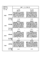
- the obtained XRT image is shown in FIG.
- FIG. 2 shows the relationship between the wavelength of the laser beam and the etching allowance and the processing strain remaining on the peripheral edge of the dot. Dots with residual processing strain on the peripheral edge are shown, while the peripheral edge is processed. Dots with no residual distortion are not shown. Further, at the bottom of each image, the ratio of the number of dots in which processing distortion remains to the total number of dots is described.
- FIG. 3 shows the relationship between the number of pulses per second of laser beam irradiation and the processing strain remaining on the periphery of the dots.
- FIG. 3 also shows XRT images of Invention Example 1 and Invention Example 2 shown in FIG. From FIG. 3, it can be seen that when the number of pulses per second is 10000, the processing distortion is removed for many dots, but the processing distortion remains for some dots. On the other hand, when the number of pulses per second of laser light irradiation is 15,000, 20,000, and 25,000, it can be seen that the processing distortion is removed for all the dots.
- the present invention it is possible to reduce the processing strain remaining on the periphery of the dots constituting the laser mark, which is useful in the semiconductor wafer manufacturing industry.
Landscapes
- Engineering & Computer Science (AREA)
- Physics & Mathematics (AREA)
- Optics & Photonics (AREA)
- Plasma & Fusion (AREA)
- Mechanical Engineering (AREA)
- Chemical & Material Sciences (AREA)
- Crystallography & Structural Chemistry (AREA)
- Materials Engineering (AREA)
- Metallurgy (AREA)
- Organic Chemistry (AREA)
- Laser Beam Processing (AREA)
- Mechanical Treatment Of Semiconductor (AREA)
- Chemical Kinetics & Catalysis (AREA)
- General Chemical & Material Sciences (AREA)
- Laser Beam Printer (AREA)
Abstract
レーザマークを構成するドット周縁に残留する加工歪みを低減することができるレーザマークの印字方法およびレーザマーク付きシリコンウェーハの製造方法を提案する。シリコンウェーハに複数のドットを有するレーザマークを印字する方法において、複数のドットの各々は、紫外領域の波長のレーザ光を用いて形成することを特徴とする。
Description
本発明は、レーザマークの印字方法およびレーザマーク付きシリコンウェーハの製造方法に関する。
従来、半導体デバイスの基板として、シリコンウェーハが広く使用されている。このシリコンウェーハは、以下のように得られる。すなわちまず、チョクラルスキー(Czochralski、CZ)法等により育成した単結晶シリコンインゴットをブロックに切断し、ブロックの外周部を研削した後、スライスする。
次いで、スライスにより得られたシリコンウェーハに対して、面取り処理、およびラップ処理、平面研削処理、両頭研削処理などの処理の1つまたは複数の処理を適宜施す。これらの処理が施されたシリコンウェーハのおもて面または裏面の外周部には、レーザ光の照射によりウェーハ管理や識別のための識別符号(マーク)を印字する場合がある。レーザ光により印字されたマーク(以下、「レーザマーク」と言う。)は、複数の凹部(ドット)の集合からなる文字や記号で構成され、目視、カメラ等により識別可能な大きさを有している。従来、上記レーザ光としては、赤外領域の波長のものが使用されている(例えば、特許文献1参照)。
上記レーザ光の照射により、ドットの周縁には環状の隆起部が形成される。そのため、上記レーザマークが印字されたシリコンウェーハの少なくともレーザマークが印字された領域(以下、「レーザマーク領域」とも言う。)に対して、エッチング処理を施して上記隆起部を除去した後、シリコンウェーハの表面に対して研磨処理を施す(例えば、特許文献2参照)。そして、研磨処理が施されたシリコンウェーハに対して最終洗浄を施し、各種検査を行って所定の品質基準を満たすものが製品として出荷される。
ところで近年、半導体デバイスの微細化、高集積化が益々進行し、シリコンウェーハには極めて高い平坦性が要求されている。また、デバイス形成領域についてもウェーハ径方向外側に年々拡大しており、ウェーハ外周部に対しても高い平坦性が要求されている。
上述のように、ドット周縁に形成された隆起部はエッチング処理により除去されている。しかしながら、本発明者の検討の結果、上述のように隆起部を除去しても、レーザ光照射の熱影響に起因するドット周縁の加工歪みが完全に除去されず、残留することが判明した。こうした加工歪みが残留した状態でシリコンウェーハに対して研磨処理を施すと、ウェーハ表面が均一に研磨されず、ウェーハ外周部の平坦度が低下するおそれがある。
本発明は上記課題を鑑みてなされたものであり、その目的とするところは、レーザマークを構成するドットの周縁に残留する加工歪みを低減することができるレーザマークの印字方法およびレーザマーク付きシリコンウェーハの製造方法を提案することにある。
上記課題を解決する本発明の要旨構成は以下の通りである。
[1]シリコンウェーハに複数のドットを有するレーザマークを印字する方法において、
前記複数のドットの各々は、紫外領域の波長のレーザ光を用いて形成することを特徴とするレーザマークの印字方法。
[1]シリコンウェーハに複数のドットを有するレーザマークを印字する方法において、
前記複数のドットの各々は、紫外領域の波長のレーザ光を用いて形成することを特徴とするレーザマークの印字方法。
[2]前記複数のドットの各々の形成は、レーザ光を複数回照射することにより行う、前記[1]に記載のレーザマークの印字方法。
[3]前記複数回のレーザ光の照射のパルス数は、1秒当たり15000以上である、前記[2]に記載のレーザマークの印字方法。
[4]所定の方法で育成した単結晶シリコンインゴットをスライスして得られたシリコンウェーハに、前記[1]~[3]のいずれかに記載のレーザマークの印字方法によりレーザマークを印字するレーザマーク印字工程と、
前記シリコンウェーハの少なくともレーザマークが印字された領域に対してエッチング処理を施すエッチング工程と、
前記エッチング工程後の前記シリコンウェーハの表面に対して研磨処理を施す研磨工程と、
を含むことを特徴とするレーザマーク付きシリコンウェーハの製造方法。
前記シリコンウェーハの少なくともレーザマークが印字された領域に対してエッチング処理を施すエッチング工程と、
前記エッチング工程後の前記シリコンウェーハの表面に対して研磨処理を施す研磨工程と、
を含むことを特徴とするレーザマーク付きシリコンウェーハの製造方法。
[5]前記エッチング工程における取り代は、片面当たり1.5μm以上である、前記[4]に記載のレーザマーク付きシリコンウェーハの製造方法。
[6]前記エッチング工程において用いる薬液は、酸またはアルカリ薬液である、前記[4]または[5]に記載のレーザマーク付きシリコンウェーハの製造方法。
本発明によれば、レーザマークを構成するドットの周縁に残留する加工歪みを低減することができる。
(レーザマークの印字方法)
以下、図面を参照して本発明の実施形態について説明する。本発明によるレーザマークの印字方法は、シリコンウェーハに複数のドットを有するレーザマークを印字する方法である。ここで、上記複数のドットの各々は、紫外領域の波長のレーザ光を用いて形成することを特徴とする。
以下、図面を参照して本発明の実施形態について説明する。本発明によるレーザマークの印字方法は、シリコンウェーハに複数のドットを有するレーザマークを印字する方法である。ここで、上記複数のドットの各々は、紫外領域の波長のレーザ光を用いて形成することを特徴とする。
上述のように、本発明者の検討の結果、エッチング処理によりレーザ光照射により形成された隆起部を除去しても、ドット周縁の加工歪みが完全に除去されずに残留し、その後の研磨処理によってウェーハ外周部の平坦度が低下することが分かった。
本発明者は、上記加工歪みを低減する方途について鋭意検討した。後述する実施例に示すように、エッチング処理における取り代を極めて大きくすれば(例えば、50μm)、ドット周縁の加工歪みを完全に除去することはできる。しかし、現在のウェーハ製造プロセスにおいて、エッチング処理における研磨代は数μm程度であるため、生産コストの点で好ましくない。
そこで本発明者は、上述のようにエッチング処理の取り代を極めて大きくしなくとも、ドット周縁の加工歪みを低減する方途について鋭意検討した。その結果、レーザマークを構成する複数のドットの各々を、紫外領域の波長のレーザ光を用いて形成することに想到したのである。
すなわち、特許文献1をはじめとする従来法においては、レーザマークを構成するドットの形成には、赤外領域の波長のレーザ光が一般的に使用されている。本発明者は、ドット周縁の加工歪みとレーザ光の波長との関係を検討した。その結果、後述する実施例に示すように、レーザ光の波長を短くすることによって加工歪みが低減されることが分かった。特に、紫外領域の波長のレーザ光を用いることによって、ドット周縁の加工歪みが大きく低減されることが判明し、本発明を完成させたのである。以下、本発明の各構成について説明する。
レーザマークを印字するシリコンウェーハは、CZ法や浮遊帯域溶融法(Floating Zone、FZ)法により育成された単結晶シリコンインゴットに対して、公知の外周研削処理、スライス処理、面取り処理、およびラップ処理、平面研削処理、両頭研削処理などの処理の1つまたは複数の処理を適宜施して得られたものを用いることができる。
上記単結晶シリコンインゴットの育成は、育成したシリコンインゴットから採取されたシリコンウェーハが所望の特性を有するように、酸素濃度や炭素濃度、窒素濃度等を適切に調整することができる。また、導電型についても、適切なドーパントを添加してn型またはp型とすることができる。
シリコンウェーハの直径は、例えば200mmとすることができるし、300mm以上(例えば、300mmや450mm)とすることもできる。また、シリコンウェーハの厚みは、仕様に応じて適切な厚み(例えば、700μm~1mm)とすることができる。
上述のように、本発明においては、レーザマークを構成する複数のドットの各々を、紫外領域の波長のレーザ光を用いて形成することが肝要である。これにより、レーザ光照射による熱影響を低減して、ドット周縁の加工歪みを低減することができる。なお、本発明において、「紫外領域の波長」とは、355nm以下の波長を意味している。
レーザ光源としては、例えばアルゴンレーザやエキシマレーザ、YAGレーザを用いることができる。このうち、レーザマーク用の光源として一般的なYAGレーザを用いることが好ましい。
1回のレーザ光の照射により形成されるドットの深さは、レーザ光の出力に依存せず、装置にもよるが、例えば2μm~10μm程度である。そのため、1回のレーザ光の照射により所望とする深さのドットを形成することができない場合には、レーザ光を複数回照射して形成してもよい。
その際、上記複数回のレーザ光の照射のパルス数は、1秒当たり10000以上とすることが好ましく、1秒当たり15000以上とすることがより好ましい。複数回のレーザ光の照射のパルス数を1秒当たり10000以上とすることにより、1回のパルスレーザ照射当たりのエネルギーを低減して、ドット周縁の加工歪みをより低減することができる。また、レーザ光照射のパルス数を1秒当たり15000以上とすることにより、ドット周縁の加工歪みをほぼ全て除去することができる。
上述のようにレーザマークが印字されたシリコンウェーハは、その後エッチング工程および研磨工程に供される。エッチング工程により、レーザマークの周縁に形成された隆起部が除去されるが、従来法に比べてドット周縁に残留する加工歪みが低減されるため、研磨工程後のシリコンウェーハ外周部の平坦性を向上させることができる。
(レーザマーク付きシリコンウェーハの製造方法)
次に、本発明によるレーザマーク付きシリコンウェーハの製造方法について説明する。図1は、本発明によるレーザマーク付きシリコンウェーハの製造方法のフローチャートを示している。この図に示すように、本発明は、CZ法やFZ法などの所定の方法で育成した単結晶シリコンインゴットをスライスし、面取り処理を施したシリコンウェーハに、上述した本発明によるレーザマークの印字方法によりレーザマークを印字するレーザマーク印字工程(ステップS1)と、上記シリコンウェーハの少なくともレーザマークが印字された領域に対してエッチング処理を施すエッチング工程(ステップS2)と、該エッチング工程後の上記シリコンウェーハの表面に対して研磨処理を施す研磨工程(ステップS3)とを含むことを特徴とする。
次に、本発明によるレーザマーク付きシリコンウェーハの製造方法について説明する。図1は、本発明によるレーザマーク付きシリコンウェーハの製造方法のフローチャートを示している。この図に示すように、本発明は、CZ法やFZ法などの所定の方法で育成した単結晶シリコンインゴットをスライスし、面取り処理を施したシリコンウェーハに、上述した本発明によるレーザマークの印字方法によりレーザマークを印字するレーザマーク印字工程(ステップS1)と、上記シリコンウェーハの少なくともレーザマークが印字された領域に対してエッチング処理を施すエッチング工程(ステップS2)と、該エッチング工程後の上記シリコンウェーハの表面に対して研磨処理を施す研磨工程(ステップS3)とを含むことを特徴とする。
まず、ステップS1のレーザマーク印字工程は、上述の本発明によるレーザマークの印字方法で行う工程と同一であるため、説明は割愛するが、複数のドットの各々を紫外領域の波長のレーザ光を用いて形成することにより、ドット周縁に残留する加工歪みを低減することができる。
上記レーザマーク印字工程の後、ステップS2において、シリコンウェーハの少なくともレーザマークが印字された領域に対してエッチング処理を施す(エッチング工程)。このエッチング工程により、ステップS1におけるレーザ光の照射により、ドットの周縁に形成された隆起部を除去するとともに、ラップ処理によりシリコンウェーハに生じた歪みを除去することもできる。
上記エッチング工程は、例えば、レーザマーク印字後のシリコンウェーハを、エッチング槽に充填されたエッチング液に浸して保持し、ウェーハを回転させながら行うことができる。
エッチング液としては、酸性またはアルカリ性のエッチング液を用いることができ、アルカリ性のエッチング液を用いることが好ましい。酸性のエッチング液としては、硝酸やフッ酸からなるエッチング液を用いることができる。また、アルカリ性のエッチング液としては、水酸化ナトリウムまたは水酸化カリウム水溶液からなるエッチング液を用いることが好ましい。このエッチング工程により、レーザマークを構成するドット部周縁の隆起部を除去するとともに、ラップ処理によりシリコンウェーハに生じた歪みを除去することもできる。
上記エッチング処理の取り代は、片面当たり0.5μm以上とすることが好ましく、1.5μm以上とすることがより好ましい。後述する実施例に示すように、エッチング処理の取り代を片面当たり1.5μmとすることにより、加工歪みをほぼ完全に除去することができる。
一方、エッチングの取り代の上限は、上述したドット周縁の加工歪みの除去やラップ処理による歪みの除去の点では特に限定されないが、製造コストの点からは15μm以下とすることが好ましい。
上記エッチング工程の後、ステップS3において、エッチング工程後のシリコンウェーハの表面に対して研磨処理を施す(研磨工程)。本研磨工程においては、砥粒を有する研磨スラリーを用いてエッチング後のウェーハの両面を研磨する。
本研磨工程は、キャリアにシリコンウェーハを嵌め込み、ウェーハを、研磨布を貼りつけた上定盤および下定盤で挟み、上下定盤とウェーハとの間に、例えばコロイダルシリカ等のスラリーを流し込み、上下定盤をキャリアに対して相対的に回転させて、シリコンウェーハの両面に対して鏡面研磨処理を施す。これにより、ウェーハ表面の凹凸を低減して平坦度の高いウェーハを得ることができる。
具体的には、研磨スラリーとしては、研磨砥粒としてコロイダルシリカを含むアルカリ性のスラリーを用いることができる。
上記研磨工程の後、シリコンウェーハの少なくとも片面を片面ずつ仕上げ研磨する片面仕上げ研磨する。この仕上げ研磨においては、片面のみの研磨および両面の研磨の両者を含む。両面を研磨する場合には、一方の表面の研磨を行った後他方の表面の研磨を行う。
その後、仕上げ研磨処理の後、研磨処理が施されたシリコンウェーハに対して洗浄する。具体的には、例えばアンモニア水、過酸化水素水および水の混合物であるSC-1洗浄液や、塩酸、過酸化水素水および水の混合物であるSC-2洗浄液を用いて、ウェーハ表面のパーティクルや有機物、金属等を除去する。
最後に、洗浄されたシリコンウェーハの平坦度、ウェーハ表面のLPDの数、ダメージ、ウェーハ表面の汚染等を検査する。この検査において所定の品質を満足するシリコンウェーハのみが製品として出荷される。
こうして、レーザマークを構成するドット周縁の加工歪みを低減することができ、外周部の平坦度が高いレーザマーク付きシリコンウェーハを製造することができる。
以下、本発明の実施例について説明するが、本発明は実施例に限定されるものではない。
<ドット周縁の加工歪みとレーザ光の波長との関係>
(発明例1~3)
図1に示したフローチャートに従って、本発明によるレーザマーク付きシリコンウェーハを作製した。まず、シリコンウェーハ外周部にレーザマークを印字した(レーザマーク印字工程)。具体的には、CZ法により育成された直径300mmの単結晶シリコンインゴットをブロックに切断し、外周研削した後、スライスした。得られたシリコンウェーハに対して面取り処理、ラップ処理を施した後、シリコンウェーハの裏面外周部に、深さ55μmの複数のドットで構成されたレーザマークを印字した。その際、レーザ光としては紫外領域の波長(355nm)のものを用いた。また、各ドットはレーザ光を18回照射することによって形成し、レーザ光照射のパルス数は、1秒当たり15000とした。
(発明例1~3)
図1に示したフローチャートに従って、本発明によるレーザマーク付きシリコンウェーハを作製した。まず、シリコンウェーハ外周部にレーザマークを印字した(レーザマーク印字工程)。具体的には、CZ法により育成された直径300mmの単結晶シリコンインゴットをブロックに切断し、外周研削した後、スライスした。得られたシリコンウェーハに対して面取り処理、ラップ処理を施した後、シリコンウェーハの裏面外周部に、深さ55μmの複数のドットで構成されたレーザマークを印字した。その際、レーザ光としては紫外領域の波長(355nm)のものを用いた。また、各ドットはレーザ光を18回照射することによって形成し、レーザ光照射のパルス数は、1秒当たり15000とした。
上述のようにシリコンウェーハ裏面外周部にレーザマークが印字されたシリコンウェーハに対してエッチング処理を施した(エッチング工程)。具体的には、エッチング液としては水酸化カリウム水溶液を用い、取り代は、片面当たり1.5μm(発明例1)、12.5μm(発明例2)および50μm(発明例3)とした。
その後、エッチング処理が施されたシリコンウェーハに対して、両面研磨処理を施した(研磨工程)。具体的には、エッチング処理が施されたシリコンウェーハをキャリアに嵌め込み、ウェーハを、研磨布を貼りつけた上定盤および下定盤で挟んだ。そして、上下定盤とウェーハとの間に、コロイダルシリカを含むアルカリ性の研磨スラリーを流し込み、上下定盤およびキャリアを互いに反対方向に回転させて、シリコンウェーハの両面に対して鏡面研磨処理を施した。この両面研磨処理での取り代は、片面で約5.0μmとした。
続いて、上記研磨処理が施されたシリコンウェーハに対して仕上げ研磨した後、洗浄して、本発明によるレーザマーク付きシリコンウェーハを得た。得られたレーザマーク付きシリコンウェーハのレーザマーク部分に対して、株式会社リガク製XRT装置を用いて、ドット周縁の加工歪みを測定した。得られたXRT画像を図2に示す。
(比較例1)
発明例1と同様に、レーザマーク付きシリコンウェーハを作製した。ただし、レーザマークを印字する際に用いたレーザ光は、赤外領域(波長1064nm)の波長のものを用いた。その他の条件は、発明例1と全て同じである。得られたXRT画像を図2に示す。
発明例1と同様に、レーザマーク付きシリコンウェーハを作製した。ただし、レーザマークを印字する際に用いたレーザ光は、赤外領域(波長1064nm)の波長のものを用いた。その他の条件は、発明例1と全て同じである。得られたXRT画像を図2に示す。
(比較例2)
発明例2と同様に、レーザマーク付きシリコンウェーハを作製した。ただし、レーザマークを印字する際に用いたレーザ光は、赤外領域(波長1064nm)の波長のものを用いた。その他の条件は、発明例2と全て同じである。得られたXRT画像を図2に示す。
発明例2と同様に、レーザマーク付きシリコンウェーハを作製した。ただし、レーザマークを印字する際に用いたレーザ光は、赤外領域(波長1064nm)の波長のものを用いた。その他の条件は、発明例2と全て同じである。得られたXRT画像を図2に示す。
(比較例3)
発明例3と同様に、レーザマーク付きシリコンウェーハを作製した。ただし、レーザマークを印字する際に用いたレーザ光は、赤外領域(波長1064nm)の波長のものを用いた。その他の条件は、発明例3と全て同じである。得られたXRT画像を図2に示す。
発明例3と同様に、レーザマーク付きシリコンウェーハを作製した。ただし、レーザマークを印字する際に用いたレーザ光は、赤外領域(波長1064nm)の波長のものを用いた。その他の条件は、発明例3と全て同じである。得られたXRT画像を図2に示す。
(比較例4)
発明例1と同様に、レーザマーク付きシリコンウェーハを作製した。ただし、レーザマークを印字する際に用いたレーザ光は、可視領域(波長532nm)の波長のものを用いた。その他の条件は、発明例1と全て同じである。得られたXRT画像を図2に示す。
発明例1と同様に、レーザマーク付きシリコンウェーハを作製した。ただし、レーザマークを印字する際に用いたレーザ光は、可視領域(波長532nm)の波長のものを用いた。その他の条件は、発明例1と全て同じである。得られたXRT画像を図2に示す。
(比較例5)
発明例2と同様に、レーザマーク付きシリコンウェーハを作製した。ただし、レーザマークを印字する際に用いたレーザ光は、可視領域(波長532nm)の波長のものを用いた。その他の条件は、発明例2と全て同じである。得られたXRT画像を図2に示す。
発明例2と同様に、レーザマーク付きシリコンウェーハを作製した。ただし、レーザマークを印字する際に用いたレーザ光は、可視領域(波長532nm)の波長のものを用いた。その他の条件は、発明例2と全て同じである。得られたXRT画像を図2に示す。
(比較例6)
発明例3と同様に、レーザマーク付きシリコンウェーハを作製した。ただし、レーザマークを印字する際に用いたレーザ光は、可視領域(波長532nm)の波長のものを用いた。その他の条件は、発明例3と全て同じである。得られたXRT画像を図2に示す。
発明例3と同様に、レーザマーク付きシリコンウェーハを作製した。ただし、レーザマークを印字する際に用いたレーザ光は、可視領域(波長532nm)の波長のものを用いた。その他の条件は、発明例3と全て同じである。得られたXRT画像を図2に示す。
図2は、レーザ光の波長およびエッチングの取り代と、ドット周縁に残留する加工歪みとの関係を示しており、周縁に加工歪みが残留しているドットが示されている一方、周縁に加工歪みが残留していないドットは示されていない。また、各画像の下方には、全体のドット数に対する加工歪みが残留しているドット数の割合が記載されている。
図2から、エッチング処理における取り代が片面当たり1.5μmおよび12.5μmであり、レーザ光の波長が1064nmおよび532nmの場合(比較例1、2、5および6)、多くのドットの周縁に加工歪みが残留していることが分かる。一方、レーザ光の波長が355nmの場合には、全てのドットについて、周縁の加工歪みが除去されていることが分かる。なお、エッチング処理における取り代が片面当たり50μmの場合には、全てのレーザ光波長についてドット周縁の加工歪みが除去されているが、現在のウェーハ製造プロセスにおける取り代は数μm程度であるため、50μmの取り代は製造コストの点で好ましくない。
<レーザ光の照射パルス数とドット周縁に残留する加工歪みとの関係>
(発明例4)
発明例1と同様に、レーザマーク付きシリコンウェーハを作製した。ただし、複数のドットを形成する際のレーザ光照射のパルス数を10000とした。その他の条件は、発明例1と全て同じである。得られたXRT画像を図3に示す。
(発明例4)
発明例1と同様に、レーザマーク付きシリコンウェーハを作製した。ただし、複数のドットを形成する際のレーザ光照射のパルス数を10000とした。その他の条件は、発明例1と全て同じである。得られたXRT画像を図3に示す。
(発明例5)
発明例2と同様に、レーザマーク付きシリコンウェーハを作製した。ただし、複数のドットを形成する際のレーザ光照射のパルス数を10000とした。その他の条件は、発明例2と全て同じである。得られたXRT画像を図3に示す。
発明例2と同様に、レーザマーク付きシリコンウェーハを作製した。ただし、複数のドットを形成する際のレーザ光照射のパルス数を10000とした。その他の条件は、発明例2と全て同じである。得られたXRT画像を図3に示す。
(発明例6)
発明例1と同様に、レーザマーク付きシリコンウェーハを作製した。ただし、複数のドットを形成する際のレーザ光照射のパルス数を20000とした。その他の条件は、発明例1と全て同じである。得られたXRT画像を図3に示す。
発明例1と同様に、レーザマーク付きシリコンウェーハを作製した。ただし、複数のドットを形成する際のレーザ光照射のパルス数を20000とした。その他の条件は、発明例1と全て同じである。得られたXRT画像を図3に示す。
(発明例7)
発明例2と同様に、レーザマーク付きシリコンウェーハを作製した。ただし、複数のドットを形成する際のレーザ光照射のパルス数を20000とした。その他の条件は、発明例2と全て同じである。得られたXRT画像を図3に示す。
発明例2と同様に、レーザマーク付きシリコンウェーハを作製した。ただし、複数のドットを形成する際のレーザ光照射のパルス数を20000とした。その他の条件は、発明例2と全て同じである。得られたXRT画像を図3に示す。
(発明例8)
発明例1と同様に、レーザマーク付きシリコンウェーハを作製した。ただし、複数のドットを形成する際のレーザ光照射のパルス数を25000とした。その他の条件は、発明例1と全て同じである。得られたXRT画像を図3に示す。
発明例1と同様に、レーザマーク付きシリコンウェーハを作製した。ただし、複数のドットを形成する際のレーザ光照射のパルス数を25000とした。その他の条件は、発明例1と全て同じである。得られたXRT画像を図3に示す。
(発明例9)
発明例2と同様に、レーザマーク付きシリコンウェーハを作製した。ただし、複数のドットを形成する際のレーザ光照射のパルス数を25000とした。その他の条件は、発明例2と全て同じである。得られたXRT画像を図3に示す。
発明例2と同様に、レーザマーク付きシリコンウェーハを作製した。ただし、複数のドットを形成する際のレーザ光照射のパルス数を25000とした。その他の条件は、発明例2と全て同じである。得られたXRT画像を図3に示す。
図3は、レーザ光照射の1秒当たりのパルス数と、ドット周縁に残留する加工歪みとの関係を示している。図3は、図2に示した発明例1および発明例2のXRT画像も示している。図3から、1秒当たりのパルス数が10000の場合には、多くのドットについて加工歪みが除去されているものの、一部のドットについては加工歪みが残留していることが分かる。一方、レーザ光照射の1秒当たりのパルス数が15000、20000および25000の場合には、全てのドットについて加工歪みが除去されていることが分かる。
本発明によれば、レーザマークを構成するドット周縁に残留する加工歪みを低減することができるため、半導体ウェーハ製造業において有用である。
Claims (6)
- シリコンウェーハに複数のドットを有するレーザマークを印字する方法において、
前記複数のドットの各々は、紫外領域の波長のレーザ光を用いて形成することを特徴とするレーザマークの印字方法。 - 前記複数のドットの各々の形成は、レーザ光を複数回照射することにより行う、請求項1に記載のレーザマークの印字方法。
- 前記複数回のレーザ光の照射のパルス数は、1秒当たり15000以上である、請求項2に記載のレーザマークの印字方法。
- 所定の方法で育成した単結晶シリコンインゴットをスライスし、面取り処理を施したシリコンウェーハに、請求項1~3のいずれかに記載のレーザマークの印字方法によりレーザマークを印字するレーザマーク印字工程と、
前記シリコンウェーハの少なくともレーザマークが印字された領域に対してエッチング処理を施すエッチング工程と、
前記エッチング工程後の前記シリコンウェーハの表面に対して研磨処理を施す研磨工程と、
を含むことを特徴とするレーザマーク付きシリコンウェーハの製造方法。 - 前記エッチング工程における取り代は、片面当たり1.5μm以上である、請求項4に記載のレーザマーク付きシリコンウェーハの製造方法。
- 前記エッチング工程において用いる薬液は、酸またはアルカリ薬液である、請求項4または5に記載のレーザマーク付きシリコンウェーハの製造方法。
Priority Applications (4)
| Application Number | Priority Date | Filing Date | Title |
|---|---|---|---|
| CN202080055930.0A CN114207780A (zh) | 2019-08-07 | 2020-07-06 | 激光标记的印刷方法及带激光标记的硅晶片的制造方法 |
| KR1020227003675A KR102716176B1 (ko) | 2019-08-07 | 2020-07-06 | 레이저 마크 부착 실리콘 웨이퍼의 제조 방법 |
| US17/633,035 US12083624B2 (en) | 2019-08-07 | 2020-07-06 | Method of printing laser mark and method of producing laser-marked silicon wafer |
| DE112020003740.1T DE112020003740T5 (de) | 2019-08-07 | 2020-07-06 | Verfahren zum drucken einer lasermarkierung und verfahren zum herstellen lasermarkierter siliziumwafer |
Applications Claiming Priority (2)
| Application Number | Priority Date | Filing Date | Title |
|---|---|---|---|
| JP2019145410A JP7205413B2 (ja) | 2019-08-07 | 2019-08-07 | レーザマーク付きシリコンウェーハの製造方法 |
| JP2019-145410 | 2019-08-07 |
Publications (1)
| Publication Number | Publication Date |
|---|---|
| WO2021024674A1 true WO2021024674A1 (ja) | 2021-02-11 |
Family
ID=74502919
Family Applications (1)
| Application Number | Title | Priority Date | Filing Date |
|---|---|---|---|
| PCT/JP2020/026461 Ceased WO2021024674A1 (ja) | 2019-08-07 | 2020-07-06 | レーザマークの印字方法およびレーザマーク付きシリコンウェーハの製造方法 |
Country Status (7)
| Country | Link |
|---|---|
| US (1) | US12083624B2 (ja) |
| JP (1) | JP7205413B2 (ja) |
| KR (1) | KR102716176B1 (ja) |
| CN (1) | CN114207780A (ja) |
| DE (1) | DE112020003740T5 (ja) |
| TW (1) | TWI775106B (ja) |
| WO (1) | WO2021024674A1 (ja) |
Families Citing this family (1)
| Publication number | Priority date | Publication date | Assignee | Title |
|---|---|---|---|---|
| CN117203173A (zh) * | 2021-04-30 | 2023-12-08 | Agc株式会社 | 导光板和导光板的制造方法 |
Citations (7)
| Publication number | Priority date | Publication date | Assignee | Title |
|---|---|---|---|---|
| JP2000263840A (ja) * | 1999-03-11 | 2000-09-26 | Hitachi Ltd | レーザ印字方法及びレーザ印字装置 |
| JP2000286173A (ja) * | 1999-03-31 | 2000-10-13 | Mitsubishi Materials Silicon Corp | ハードレーザマーキングウェーハおよびその製造方法 |
| JP2003188059A (ja) * | 2001-12-01 | 2003-07-04 | Eo Technics Co Ltd | チップスケールマーカのマーキング位置補正方法及びその装置 |
| JP2008504964A (ja) * | 2004-06-30 | 2008-02-21 | ジーエスアイ ルモニクス コーポレーション | ターゲット表面材料を加工するレーザベース方法およびシステム並びにその製造物 |
| JP2011029355A (ja) * | 2009-07-24 | 2011-02-10 | Sumco Corp | レーザマーク付き半導体ウェーハの製造方法 |
| JP2013093493A (ja) * | 2011-10-27 | 2013-05-16 | Sumitomo Electric Ind Ltd | 半導体装置の製造方法 |
| JP2014036134A (ja) * | 2012-08-09 | 2014-02-24 | Disco Abrasive Syst Ltd | デバイスの加工方法 |
Family Cites Families (21)
| Publication number | Priority date | Publication date | Assignee | Title |
|---|---|---|---|---|
| JP2924861B2 (ja) | 1997-06-11 | 1999-07-26 | 日本電気株式会社 | 半導体ウエハ用レーザマーキング装置およびその方法 |
| US6037259A (en) * | 1998-05-11 | 2000-03-14 | Vanguard International Semiconductor Corporation | Method for forming identifying characters on a silicon wafer |
| JP2001219386A (ja) * | 2000-02-08 | 2001-08-14 | Sumitomo Metal Ind Ltd | レーザマーク付き半導体ウエーハ製造方法 |
| US7157038B2 (en) * | 2000-09-20 | 2007-01-02 | Electro Scientific Industries, Inc. | Ultraviolet laser ablative patterning of microstructures in semiconductors |
| JP2002346772A (ja) * | 2001-05-21 | 2002-12-04 | Sumitomo Mitsubishi Silicon Corp | レーザマーキングウェーハ |
| JP3980465B2 (ja) | 2001-11-09 | 2007-09-26 | 株式会社半導体エネルギー研究所 | 半導体装置の作製方法 |
| US7416962B2 (en) * | 2002-08-30 | 2008-08-26 | Siltronic Corporation | Method for processing a semiconductor wafer including back side grinding |
| DE102004023967B3 (de) * | 2004-05-14 | 2005-12-08 | Forschungszentrum Karlsruhe Gmbh | Röhrenkollektor zur Abscheidung elektrisch geladener Aerosole aus einem Gasstrom |
| KR100735528B1 (ko) | 2006-02-07 | 2007-07-04 | 삼성전자주식회사 | 반도체 소자 제조용 장비, 반도체 소자의 제조 방법,웨이퍼 |
| JP2007234945A (ja) * | 2006-03-02 | 2007-09-13 | Toshiba Ceramics Co Ltd | レーザーマーキングウェーハおよびその製造方法 |
| KR20090107494A (ko) * | 2006-12-05 | 2009-10-13 | 나노 테라 인코포레이티드 | 표면을 패턴화하는 방법 |
| CN101670492A (zh) * | 2009-09-16 | 2010-03-17 | 苏州德龙激光有限公司 | Led晶圆三光束激光划片设备的设计方法 |
| JP2011187706A (ja) * | 2010-03-09 | 2011-09-22 | Sumco Corp | シリコンウェーハの製造方法 |
| WO2012075072A2 (en) * | 2010-11-30 | 2012-06-07 | Corning Incorporated | Methods of forming high-density arrays of holes in glass |
| JP2012183549A (ja) * | 2011-03-04 | 2012-09-27 | Mitsubishi Electric Corp | SiC半導体ウェハのマーキング方法およびSiC半導体ウェハ |
| US20170236954A1 (en) * | 2011-08-05 | 2017-08-17 | Beamreach | High efficiency solar cell structures and manufacturing methods |
| JP6572863B2 (ja) * | 2016-10-18 | 2019-09-11 | 信越半導体株式会社 | シリコンウェーハの製造方法 |
| JP6855955B2 (ja) * | 2017-06-19 | 2021-04-07 | 株式会社Sumco | レーザマークの印字方法、レーザマーク付きシリコンウェーハの製造方法 |
| CN108682647B (zh) | 2018-07-16 | 2024-02-02 | 华侨大学 | 晶片侧面打码读码存储一体机及其使用方法 |
| JP6717353B2 (ja) * | 2018-10-22 | 2020-07-01 | 株式会社Sumco | レーザマーク付きシリコンウェーハの製造方法 |
| CN110255492A (zh) * | 2019-05-31 | 2019-09-20 | 北京工商大学 | 一种硅基底超疏水超亲水区域分布表面及其制备方法和应用 |
-
2019
- 2019-08-07 JP JP2019145410A patent/JP7205413B2/ja active Active
-
2020
- 2020-07-06 WO PCT/JP2020/026461 patent/WO2021024674A1/ja not_active Ceased
- 2020-07-06 US US17/633,035 patent/US12083624B2/en active Active
- 2020-07-06 CN CN202080055930.0A patent/CN114207780A/zh active Pending
- 2020-07-06 KR KR1020227003675A patent/KR102716176B1/ko active Active
- 2020-07-06 DE DE112020003740.1T patent/DE112020003740T5/de active Granted
- 2020-07-07 TW TW109122878A patent/TWI775106B/zh active
Patent Citations (7)
| Publication number | Priority date | Publication date | Assignee | Title |
|---|---|---|---|---|
| JP2000263840A (ja) * | 1999-03-11 | 2000-09-26 | Hitachi Ltd | レーザ印字方法及びレーザ印字装置 |
| JP2000286173A (ja) * | 1999-03-31 | 2000-10-13 | Mitsubishi Materials Silicon Corp | ハードレーザマーキングウェーハおよびその製造方法 |
| JP2003188059A (ja) * | 2001-12-01 | 2003-07-04 | Eo Technics Co Ltd | チップスケールマーカのマーキング位置補正方法及びその装置 |
| JP2008504964A (ja) * | 2004-06-30 | 2008-02-21 | ジーエスアイ ルモニクス コーポレーション | ターゲット表面材料を加工するレーザベース方法およびシステム並びにその製造物 |
| JP2011029355A (ja) * | 2009-07-24 | 2011-02-10 | Sumco Corp | レーザマーク付き半導体ウェーハの製造方法 |
| JP2013093493A (ja) * | 2011-10-27 | 2013-05-16 | Sumitomo Electric Ind Ltd | 半導体装置の製造方法 |
| JP2014036134A (ja) * | 2012-08-09 | 2014-02-24 | Disco Abrasive Syst Ltd | デバイスの加工方法 |
Also Published As
| Publication number | Publication date |
|---|---|
| JP2021027243A (ja) | 2021-02-22 |
| DE112020003740T5 (de) | 2022-04-28 |
| KR102716176B1 (ko) | 2024-10-11 |
| US20220331906A1 (en) | 2022-10-20 |
| JP7205413B2 (ja) | 2023-01-17 |
| TW202120756A (zh) | 2021-06-01 |
| KR20220025085A (ko) | 2022-03-03 |
| CN114207780A (zh) | 2022-03-18 |
| US12083624B2 (en) | 2024-09-10 |
| TWI775106B (zh) | 2022-08-21 |
Similar Documents
| Publication | Publication Date | Title |
|---|---|---|
| JP3658454B2 (ja) | 半導体ウェハの製造方法 | |
| US11515263B2 (en) | Method of producing laser-marked silicon wafer and laser-marked silicon wafer | |
| CN109148260B (zh) | 激光标记的刻印方法、带激光标记的硅晶片及其制造方法 | |
| JP2011029355A (ja) | レーザマーク付き半導体ウェーハの製造方法 | |
| JP2011003773A (ja) | シリコンウェーハの製造方法 | |
| WO2018116558A1 (ja) | シリコンウェーハの研磨方法およびシリコンウェーハの製造方法 | |
| TWI680512B (zh) | 矽晶圓之研磨方法、矽晶圓之製造方法及矽晶圓 | |
| JP7205413B2 (ja) | レーザマーク付きシリコンウェーハの製造方法 | |
| JP4492293B2 (ja) | 半導体基板の製造方法 | |
| JP4342631B2 (ja) | ハードレーザマーキングウェーハの製造方法 | |
| US6211088B1 (en) | Manufacturing method for semiconductor gas-phase epitaxial wafer | |
| JP3787485B2 (ja) | 薄板の加工方法 | |
| WO2011021349A1 (ja) | シリコンエピタキシャルウェーハの製造方法 | |
| JP2010171330A (ja) | エピタキシャルウェハの製造方法、欠陥除去方法およびエピタキシャルウェハ | |
| WO2022224637A1 (ja) | シリコンウェーハの製造方法 | |
| KR100918076B1 (ko) | 플라즈마 처리 장치용 실리콘 소재의 제조 방법 | |
| JP2011091143A (ja) | シリコンエピタキシャルウェーハの製造方法 | |
| JP2002134521A (ja) | シリコン半導体基板の熱処理方法 | |
| JP5810907B2 (ja) | 基板の再生方法及び該再生方法を用いた窒化物半導体素子の製造方法 | |
| JP2009182243A (ja) | 半導体結晶ウェハの面取部の鏡面加工方法およびその方法で得られるウェハ | |
| JP2002173398A (ja) | ランガサイト型酸化物単結晶ウェハの製造方法 | |
| JPH07283176A (ja) | 半導体ウェハの研磨方法 | |
| JP2003218066A (ja) | 半導体ウェーハの研磨方法 | |
| KR20130080321A (ko) | 실리콘 웨이퍼 제조 방법 |
Legal Events
| Date | Code | Title | Description |
|---|---|---|---|
| 121 | Ep: the epo has been informed by wipo that ep was designated in this application |
Ref document number: 20849398 Country of ref document: EP Kind code of ref document: A1 |
|
| ENP | Entry into the national phase |
Ref document number: 20227003675 Country of ref document: KR Kind code of ref document: A |
|
| 122 | Ep: pct application non-entry in european phase |
Ref document number: 20849398 Country of ref document: EP Kind code of ref document: A1 |