WO2020255878A1 - 可撓性基板とバスバとの接続構造、配線モジュールおよび蓄電モジュール - Google Patents
可撓性基板とバスバとの接続構造、配線モジュールおよび蓄電モジュール Download PDFInfo
- Publication number
- WO2020255878A1 WO2020255878A1 PCT/JP2020/023220 JP2020023220W WO2020255878A1 WO 2020255878 A1 WO2020255878 A1 WO 2020255878A1 JP 2020023220 W JP2020023220 W JP 2020023220W WO 2020255878 A1 WO2020255878 A1 WO 2020255878A1
- Authority
- WO
- WIPO (PCT)
- Prior art keywords
- bus bar
- land
- connection
- base material
- metal
- Prior art date
Links
Images


Classifications
-
- H—ELECTRICITY
- H01—ELECTRIC ELEMENTS
- H01M—PROCESSES OR MEANS, e.g. BATTERIES, FOR THE DIRECT CONVERSION OF CHEMICAL ENERGY INTO ELECTRICAL ENERGY
- H01M50/00—Constructional details or processes of manufacture of the non-active parts of electrochemical cells other than fuel cells, e.g. hybrid cells
- H01M50/50—Current conducting connections for cells or batteries
- H01M50/502—Interconnectors for connecting terminals of adjacent batteries; Interconnectors for connecting cells outside a battery casing
- H01M50/505—Interconnectors for connecting terminals of adjacent batteries; Interconnectors for connecting cells outside a battery casing comprising a single busbar
-
- H—ELECTRICITY
- H01—ELECTRIC ELEMENTS
- H01M—PROCESSES OR MEANS, e.g. BATTERIES, FOR THE DIRECT CONVERSION OF CHEMICAL ENERGY INTO ELECTRICAL ENERGY
- H01M50/00—Constructional details or processes of manufacture of the non-active parts of electrochemical cells other than fuel cells, e.g. hybrid cells
- H01M50/50—Current conducting connections for cells or batteries
- H01M50/502—Interconnectors for connecting terminals of adjacent batteries; Interconnectors for connecting cells outside a battery casing
- H01M50/519—Interconnectors for connecting terminals of adjacent batteries; Interconnectors for connecting cells outside a battery casing comprising printed circuit boards [PCB]
-
- H—ELECTRICITY
- H01—ELECTRIC ELEMENTS
- H01M—PROCESSES OR MEANS, e.g. BATTERIES, FOR THE DIRECT CONVERSION OF CHEMICAL ENERGY INTO ELECTRICAL ENERGY
- H01M50/00—Constructional details or processes of manufacture of the non-active parts of electrochemical cells other than fuel cells, e.g. hybrid cells
- H01M50/20—Mountings; Secondary casings or frames; Racks, modules or packs; Suspension devices; Shock absorbers; Transport or carrying devices; Holders
- H01M50/284—Mountings; Secondary casings or frames; Racks, modules or packs; Suspension devices; Shock absorbers; Transport or carrying devices; Holders with incorporated circuit boards, e.g. printed circuit boards [PCB]
-
- H—ELECTRICITY
- H01—ELECTRIC ELEMENTS
- H01M—PROCESSES OR MEANS, e.g. BATTERIES, FOR THE DIRECT CONVERSION OF CHEMICAL ENERGY INTO ELECTRICAL ENERGY
- H01M50/00—Constructional details or processes of manufacture of the non-active parts of electrochemical cells other than fuel cells, e.g. hybrid cells
- H01M50/20—Mountings; Secondary casings or frames; Racks, modules or packs; Suspension devices; Shock absorbers; Transport or carrying devices; Holders
- H01M50/204—Racks, modules or packs for multiple batteries or multiple cells
- H01M50/207—Racks, modules or packs for multiple batteries or multiple cells characterised by their shape
- H01M50/209—Racks, modules or packs for multiple batteries or multiple cells characterised by their shape adapted for prismatic or rectangular cells
-
- H—ELECTRICITY
- H01—ELECTRIC ELEMENTS
- H01M—PROCESSES OR MEANS, e.g. BATTERIES, FOR THE DIRECT CONVERSION OF CHEMICAL ENERGY INTO ELECTRICAL ENERGY
- H01M50/00—Constructional details or processes of manufacture of the non-active parts of electrochemical cells other than fuel cells, e.g. hybrid cells
- H01M50/50—Current conducting connections for cells or batteries
- H01M50/502—Interconnectors for connecting terminals of adjacent batteries; Interconnectors for connecting cells outside a battery casing
- H01M50/503—Interconnectors for connecting terminals of adjacent batteries; Interconnectors for connecting cells outside a battery casing characterised by the shape of the interconnectors
-
- H—ELECTRICITY
- H01—ELECTRIC ELEMENTS
- H01M—PROCESSES OR MEANS, e.g. BATTERIES, FOR THE DIRECT CONVERSION OF CHEMICAL ENERGY INTO ELECTRICAL ENERGY
- H01M50/00—Constructional details or processes of manufacture of the non-active parts of electrochemical cells other than fuel cells, e.g. hybrid cells
- H01M50/50—Current conducting connections for cells or batteries
- H01M50/502—Interconnectors for connecting terminals of adjacent batteries; Interconnectors for connecting cells outside a battery casing
- H01M50/507—Interconnectors for connecting terminals of adjacent batteries; Interconnectors for connecting cells outside a battery casing comprising an arrangement of two or more busbars within a container structure, e.g. busbar modules
-
- H—ELECTRICITY
- H01—ELECTRIC ELEMENTS
- H01M—PROCESSES OR MEANS, e.g. BATTERIES, FOR THE DIRECT CONVERSION OF CHEMICAL ENERGY INTO ELECTRICAL ENERGY
- H01M50/00—Constructional details or processes of manufacture of the non-active parts of electrochemical cells other than fuel cells, e.g. hybrid cells
- H01M50/50—Current conducting connections for cells or batteries
- H01M50/502—Interconnectors for connecting terminals of adjacent batteries; Interconnectors for connecting cells outside a battery casing
- H01M50/514—Methods for interconnecting adjacent batteries or cells
- H01M50/516—Methods for interconnecting adjacent batteries or cells by welding, soldering or brazing
-
- H—ELECTRICITY
- H01—ELECTRIC ELEMENTS
- H01M—PROCESSES OR MEANS, e.g. BATTERIES, FOR THE DIRECT CONVERSION OF CHEMICAL ENERGY INTO ELECTRICAL ENERGY
- H01M50/00—Constructional details or processes of manufacture of the non-active parts of electrochemical cells other than fuel cells, e.g. hybrid cells
- H01M50/50—Current conducting connections for cells or batteries
- H01M50/502—Interconnectors for connecting terminals of adjacent batteries; Interconnectors for connecting cells outside a battery casing
- H01M50/521—Interconnectors for connecting terminals of adjacent batteries; Interconnectors for connecting cells outside a battery casing characterised by the material
- H01M50/522—Inorganic material
-
- H—ELECTRICITY
- H01—ELECTRIC ELEMENTS
- H01M—PROCESSES OR MEANS, e.g. BATTERIES, FOR THE DIRECT CONVERSION OF CHEMICAL ENERGY INTO ELECTRICAL ENERGY
- H01M50/00—Constructional details or processes of manufacture of the non-active parts of electrochemical cells other than fuel cells, e.g. hybrid cells
- H01M50/50—Current conducting connections for cells or batteries
- H01M50/569—Constructional details of current conducting connections for detecting conditions inside cells or batteries, e.g. details of voltage sensing terminals
-
- H—ELECTRICITY
- H05—ELECTRIC TECHNIQUES NOT OTHERWISE PROVIDED FOR
- H05K—PRINTED CIRCUITS; CASINGS OR CONSTRUCTIONAL DETAILS OF ELECTRIC APPARATUS; MANUFACTURE OF ASSEMBLAGES OF ELECTRICAL COMPONENTS
- H05K1/00—Printed circuits
- H05K1/02—Details
- H05K1/14—Structural association of two or more printed circuits
-
- H—ELECTRICITY
- H05—ELECTRIC TECHNIQUES NOT OTHERWISE PROVIDED FOR
- H05K—PRINTED CIRCUITS; CASINGS OR CONSTRUCTIONAL DETAILS OF ELECTRIC APPARATUS; MANUFACTURE OF ASSEMBLAGES OF ELECTRICAL COMPONENTS
- H05K3/00—Apparatus or processes for manufacturing printed circuits
- H05K3/36—Assembling printed circuits with other printed circuits
-
- H—ELECTRICITY
- H01—ELECTRIC ELEMENTS
- H01M—PROCESSES OR MEANS, e.g. BATTERIES, FOR THE DIRECT CONVERSION OF CHEMICAL ENERGY INTO ELECTRICAL ENERGY
- H01M2220/00—Batteries for particular applications
- H01M2220/20—Batteries in motive systems, e.g. vehicle, ship, plane
Definitions
- the present disclosure relates to a connection structure between a flexible substrate and a bus bar, a wiring module, and a power storage module.
- a composite flexible printed wiring board in which a plurality of flexible printed wiring boards are joined is known as described in Japanese Patent Application Laid-Open No. 2019-29534 (Patent Document 1 below).
- the flexible printed wiring board has a metal block made of copper connected to a conductor layer.
- a plurality of flexible printed wiring boards are joined by laser welding or resistance welding of metal blocks.
- Aluminum or aluminum alloy is being considered as the metal for Basba.
- the metal of the land and the metal of the bus bar are joined at the joint where the connection portion and the bus bar are joined by welding.
- An intermetallic compound composed of is produced. If an intermetallic compound portion is formed at the joint portion, the joint portion becomes brittle and the joint strength between the flexible printed wiring board and the bus bar is lowered.
- the land and bus bar 502 of the flexible printed wiring board 501 and the relay member 503 containing nickel having high bonding strength are bridged between the flexible printed wiring board 501 and the bus bar 502.
- a method is conceivable in which the land and the relay member 3 are joined by soldering or the like, and the bus bar 502 and the relay member 503 are joined by welding.
- the flexible printed wiring board 501 and the bus bar 502 can be electrically connected while improving the joint strength of the joint portion between the flexible printed wiring board 501 and the bus bar 502 and the relay member 503.
- the relay member is tilted between the flexible printed wiring board and the bus bar. Therefore, it is necessary to align the flexible printed wiring board and the bus bar with the relay member. Even if the alignment is performed in advance, if the thickness of the flexible printed wiring board or bus bar changes due to manufacturing tolerances, the relay member will be joined in an inclined state, and the joining strength will be increased. Will decrease.
- This specification discloses a technique for electrically connecting two members while improving the joining strength of the joining portion.
- connection structure between the flexible substrate and the bus bar of the present disclosure includes a flexible substrate, at least one bus bar, and at least one connection piece, and the flexible substrate includes a plurality of first metals.
- the conductive path is formed by being covered with a flexible resin base material having an insulating property, and the bus bar is formed in a plate shape containing a second metal different from the first metal, and the conductive path is formed.
- the path has a first conductive path and a second conductive path extending from the first conductive path, and the resin base material has a strip-shaped main base material and branches from the main base material and extends onto the bus bar.
- the main base material has at least one said first conductive path
- the sub-base material has at least one said second conductive path.
- the second conductive path has a connecting land exposed from the sub-base material
- the connecting piece is different from the first metal and the second metal and is welded between the first metal and the second metal. It is formed in a plate shape containing a third metal having a higher bonding strength in welding with the second metal than the bonding strength in the above, the bus bar is joined to the connecting piece by welding, and the connecting land is the said. It is joined by a connecting piece and a wax joint.
- two members can be electrically connected while improving the joint strength of the joint portion.
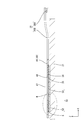
- FIG. 1 is a schematic view showing a vehicle equipped with the power storage module according to the first embodiment.
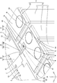
- FIG. 2 is a partial perspective view of the power storage module of the first embodiment.
- FIG. 3 is a partial plan view of the power storage module.
- FIG. 4 is a cross-sectional view taken along the line AA of FIG.
- FIG. 5 is an enlarged cross-sectional view of a main part of FIG.
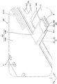
- FIG. 6 is a partial perspective view of the wiring module assembling process, and is a partial perspective view showing a state before the connection piece is placed on the connection land.
- FIG. 7 is a partial perspective view of the wiring module assembling process, and is a partial plan view showing a state before the bent portion is bent.
- FIG. 8 is a partial perspective view of the wiring module of the second embodiment.
- FIG. 1 is a schematic view showing a vehicle equipped with the power storage module according to the first embodiment.
- FIG. 2 is a partial perspective view of the power storage module of the first embodiment.
- FIG. 9 is a partial perspective view of the wiring module of the third embodiment.
- FIG. 10 is an enlarged cross-sectional view of a main part corresponding to the cross section of FIG. 5 in FIG.
- FIG. 11 is a partial perspective view of the wiring module of the fourth embodiment.
- FIG. 12 is an enlarged cross-sectional view of a main part corresponding to the cross section of FIG. 5 in FIG.
- FIG. 13 is a partial perspective view of the wiring module of the fifth embodiment.
- FIG. 14 is an enlarged cross-sectional view of a main part corresponding to the cross section of FIG. 5 in FIG.
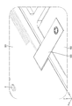
- FIG. 15 is a partial perspective view of a wiring module that connects the FPC and the bus bar by bridging a relay member.
- a flexible resin comprising a flexible substrate, at least one bus bar, and at least one connecting piece, wherein the flexible substrate is a flexible resin in which a plurality of conductive paths containing a first metal have insulating properties. It is formed by being covered with a base material, and the bus bar is formed in a plate shape containing a second metal different from the first metal, and the conductive paths are a first conductive path and a first conductive path. It has a second conductive path extending from the path, and the resin base material has a strip-shaped main base material and a sub-base material that branches from the main base material and extends onto the bus bar.
- At least one of the first conductive paths is arranged on the base material, at least one of the second conductive paths is arranged on the sub-base material, and the second conductive path is the sub-group. It has a connecting land exposed from the material, and the connecting piece is different from the first metal and the second metal, and is welded to the second metal rather than the bonding strength in the welding of the first metal and the second metal. It is formed in a plate shape containing a third metal having a high bonding strength in the above, the bus bar is joined to the connecting piece by welding, and the connecting land is joined to the connecting piece by brazing.
- the exposed connecting lands in the sub-base material of the flexible substrate extend over the bus bar, and the connecting lands and bus bars are joined in the welding with the second metal rather than the joining strength in the welding between the first metal and the second metal. It is joined via a connecting piece formed containing a high-strength tertiary metal. That is, the flexible substrate and the bus bar can be electrically connected while improving the bonding strength in welding the bus bar and the connecting piece.
- welding in the present specification is to melt at least one base material of two base materials and integrate them so as to have continuity between the two base materials. Different joining means. Specific means of welding include, for example, laser welding, resistance welding, ultrasonic welding and the like.
- the second conductive path can be arranged between the flexible substrate and the bus bar by bending the sub-base material.
- the connection land and the bus bar can be connected without having to align the flexible substrate and the bus bar in advance. That is, unlike the case where a relay member is bridged between the flexible substrate and the bus bar to connect the flexible substrate and the bus bar, for example, the connection piece does not tilt between the connection land and the bus bar. , It is possible to prevent the joint strength between the connection land and the bus bar and the connection piece from being lowered.
- connection land arranged on the bus bar and the bus bar are connected via the connection piece, the size of the connection piece is larger than, for example, when a relay member is bridged between the flexible substrate and the bus bar. Can be reduced and the manufacturing cost can be reduced.
- connection piece has a land connection portion and a bus bar connection portion
- the third metal is a metal in which an oxide film is less likely to be formed on the surface than the second metal.
- the land connection portion is joined to the connection land by brazing
- the bus bar connection portion is joined to the bus bar by welding.
- brazing means that a filler material such as a brazing material or solder is melted and integrated so that there is continuity between the two base materials without melting the base material. For example, brazing, Brazing and the like can be mentioned.
- the joint strength in welding between the bus bar and the bus bar connection portion can be increased by forming the connection piece with the same metal as the bus bar.
- the bonding strength between the land connection portion and the connection land is lowered unless the oxide film is removed from the bonding by brazing.
- the connection piece is formed by containing a third metal, which is more difficult to form an oxide film than Basba, the land connection portion and the connection land are joined by waxing without the treatment of removing the oxide film. The strength can be increased.
- connection piece and the connection land, and the connection piece and the bus bar can be individually joined without aligning the connection pieces with respect to the two members. That is, for example, as compared with the case where the connection pieces are joined to the two members at the same time, the positional deviation of the connection pieces with respect to the connection land and the bus bar can be suppressed, and the joint strength of the joint portion is lowered due to the positional deviation. Can be suppressed.
- the first metal is copper, the second metal is aluminum, and the third metal is nickel.
- the first metal is aluminum, the second metal is copper, and the third metal is nickel.
- copper or a copper alloy is used for the conductive path and bus bar of a flexible substrate such as a flexible printed circuit board or a flexible flat cable.
- aluminum or aluminum alloy has been studied as a metal used for a flexible printed circuit board, a conductive path of a flexible flat cable, and a bus bar.
- the present inventors have found that the bonding strength between nickel and copper and the bonding strength between nickel and aluminum are higher than the bonding strength between copper and aluminum. That is, since the connection piece is formed containing nickel, the joint strength in the brazing joint between the connection land and the land connection portion is improved, and the joint strength in the weld joint between the bus bar and the bus bar connection portion is improved. Can be done.
- the connecting land is formed so as to be exposed on the surface of the sub-base material on the bus bar side, and the land connecting portion is arranged between the connecting land and the bus bar.
- the connecting portion is arranged so as to be exposed from the sub-base material.
- the bus bar connection can be welded to the bus bar using the part exposed from the sub-base material as a mark. Therefore, it is possible to prevent the joint position at the bus bar connection portion from being displaced with respect to the bus bar. As a result, it is possible to prevent the joint strength between the bus bar connection portion and the bus bar from being lowered due to the misalignment of the joint portion.
- the connecting land when the connecting land is exposed on the surface of the sub-base material opposite to the bus bar side, the position of the connecting land and the position of the bus bar are displaced in the thickness direction of the flexible substrate. It ends up. Therefore, it is necessary to process the connection piece in order to align the land connection portion and the bus bar connection portion.
- the position of the land connection portion and the position of the bus bar connection portion do not deviate in the thickness direction of the flexible substrate, so that the flexible substrate and the bus bar are electrically connected without processing the connection piece. Can be connected.
- the main base material has a bent portion that is bent toward the sub base material and is connected to the sub base material.
- a part of the main base material is bent to form the sub base material. Therefore, the yield of the flexible substrate can be improved as compared with the case where the sub-base material forms the flexible substrate protruding from the main base material from the beginning.
- connection piece and the electronic component are arranged on the connection land, the electronic component is arranged on the first conductive path, and the flexible substrate is passed through the reflow furnace. Are collectively connected to the flexible substrate. Then, by forming the bent portion, the connecting piece is arranged between the connecting land and the bus bar. That is, since the connection piece and the electronic component can be solder-bonded together, the work man-hours can be reduced and the manufacturing cost can be reduced as compared with the case where the connection piece and the electronic component are individually solder-bonded, for example.
- connection land is formed so as to be exposed on the surface of the sub-base material on the bus bar side, and the surface of the bus bar connection portion is recessed on the side opposite to the bus bar and the surface on the bus bar side. Projects toward the bus bar.
- the bus bar connection can be welded to the bus bar using the recessed part as a mark. Therefore, it is possible to prevent the joint position at the bus bar connection portion from being displaced with respect to the bus bar. As a result, it is possible to prevent the joint strength between the bus bar connection portion and the bus bar from being lowered due to the misalignment of the joint portion.
- the sub-base material has a base material through hole penetrating in the plate thickness direction, and the connecting land penetrates in the plate thickness direction and is arranged coaxially with the base material through hole. It has a through hole, and the bus bar connection portion is exposed through the base material through hole and the land through hole.
- the bus bar connection portion can be welded to the bus bar by using the portion exposed from the base material through hole and the land through hole as a mark. Therefore, it is possible to prevent the joint position at the bus bar connection portion from being displaced with respect to the bus bar. As a result, it is possible to prevent the joint strength between the bus bar connection portion and the bus bar from being lowered due to the misalignment of the joint portion.
- a plurality of power storage elements having electrode terminals are arranged in a state of holding the connection structure between the flexible substrate and the bus bar, and at least one flexible substrate and the plurality of bus bars.
- the bus bar is provided with an insulating protector attached to the power storage element group, and the bus bar is joined to the electrode terminal by welding.
- the wiring module is a wiring module for a vehicle that is mounted on a vehicle and used.
- the power storage module includes the wiring module and the power storage element group.
- connection structure between the flexible substrate and the bus bar of the present disclosure, the wiring module, and the power storage module will be described with reference to the following drawings. It should be noted that the present disclosure is not limited to these examples, and is indicated by the scope of claims, and is intended to include all modifications within the meaning and scope equivalent to the scope of claims.
- the first embodiment to which the present disclosure is applied to the storage pack 2 mounted on the vehicle 1 will be described with reference to FIGS. 1 to 7.
- the power storage pack 2 is mounted on a vehicle 1 such as an electric vehicle or a hybrid vehicle and is used as a drive source for the vehicle 1.
- vehicle 1 such as an electric vehicle or a hybrid vehicle
- the reference numerals of other members may be omitted.
- a power storage pack 2 is arranged near the center of the vehicle 1.
- a PCU 3 Power Control Unit
- the power storage pack 2 and the PCU 3 are connected by a wire harness 4.
- the power storage pack 2 and the wire harness 4 are connected by a connector (not shown).
- the power storage pack 2 has a power storage module 10 including a plurality of power storage elements 71.
- the power storage module 10 includes a power storage element group 70 and a wiring module 20. 2 and 3 show a part of the power storage module 10.
- the power storage element group 70 includes a plurality of power storage elements 71 arranged in the front-rear direction.
- Each power storage element 71 is, for example, a secondary battery.
- a pair of electrode terminals 73 are arranged at positions on the upper surface of each power storage element 71 near both ends in the left-right direction. The right electrode of the electrode terminals 73 is omitted in the figure.
- the two power storage elements 71 adjacent to each other in the front-rear direction are arranged so that the polarities of the adjacent electrode terminals 73 are different.
- the electrode terminal 73 is formed flat so that the bus bar 21 of the wiring module 20 described later can be mounted.
- the wiring module 20 is attached to the power storage element group 70 from above, and includes a bus bar 21, a flexible printed circuit board (an example of a "flexible board") 30, a bus bar 21, and a flexible printed circuit board 30.
- the connection piece 50 for connecting the above and the insulation protector 60 are provided.
- bus bar 21 As shown in FIG. 3, the bus bar 21 is formed into a flat plate having a rectangular shape in a plan view by processing a conductive metal plate material.
- the bus bar 21 is formed by processing a metal plate material containing aluminum such as aluminum and an aluminum alloy.
- the bus bar 21 is formed in a size that covers the electrode terminals 73 adjacent to each other in the front-rear direction in the power storage element group 70.
- the bus bar 21 is placed on the electrode terminals 73 so as to straddle the electrode terminals 73 adjacent to each other in the front-rear direction.
- the bus bar 21 mounted on the electrode terminal 73 is joined to the electrode terminal 73 in a circular shape by laser welding.
- a circular welding mark M is formed on the bus bar 21.
- the bus bar 21 and the electrode terminal 73 are electrically connected and fixed to each other. The laser welding may be performed linearly instead of circularly.
- the bus bar 21 and the electrode terminal 73 are formed by melting the bus bar 21 which is the base material of at least one of the bus bar 21 and the electrode terminal 73. Are integrated so that there is continuity.
- the flexible printed circuit board (hereinafter, also simply referred to as “FPC”) 30 is a member for electrically connecting a bus bar 21 and an electronic control unit (not shown) and transmitting current, temperature, and voltage applied to the bus bar 21 to the ECU.
- the electronic control unit is equipped with a microcomputer, electronic elements, etc., and is used to detect the voltage, current, temperature, etc. of the power storage element 71 transmitted through the FPC 30, and to control the charge / discharge of the power storage element group 70. It is a well-known one with the functions of.
- the FPC 30 includes a main board 30A extending in the front-rear direction over the entire length of the power storage element group 70 along the front-rear direction which is the arrangement direction of the power storage elements 71, and a left side from the main board 30A. It has a sub-board 30B protruding toward. Further, the FPC 30 includes an insulating film (an example of a “resin base material”) 40, a plurality of conductive paths 31, and an electronic component E.
- insulating film an example of a “resin base material”
- the insulating film 40 is made of a synthetic resin such as polyimide having flexibility and insulating properties, and covers the conductive path 31 from both sides in the vertical direction. As shown in FIGS. 2 and 3, the insulating film 40 has a main film portion (an example of a “main base material”) 41 and a sub film portion (an example of a “sub base material”) 46. ..
- the main film portion 41 is formed so as to extend in a band shape in the front-rear direction over the entire length of the power storage element group 70 along the front-rear direction which is the arrangement direction of the power storage elements 71.
- the main film portion 41 constitutes the main substrate 30A together with the first conductive paths 32 of the plurality of conductive paths 31 described later.
- An electronic component E is mounted on the main film portion 41. Although not shown in detail, the electronic component E is electrically connected to the first conductive path 32 of the conductive path 31, which will be described later, by soldering. As the electronic component E, any electronic component such as a resistor, a capacitor, a transistor, or a microcomputer is appropriately selected.
- a sub-film portion 46 is formed at the left end portion of the main film portion 41 so as to project to the left from the main film portion 41 by making a notch and bending the notched portion to the left. There is.
- the bent portion of the main film portion 41 is a bent portion 42 that is bent toward the left so that the portion configured as the sub film portion 46 is turned upside down. Therefore, as shown in FIGS. 2 and 3, a notch 43 having substantially the same size as the sub film portion 46 is formed at the left end portion of the main film portion 41.
- the notch 43 is formed in an L-shape in a plan view extending in the front-rear direction and extending to the right, and a bent portion 42 is formed at the rear end of the notch 43.
- Sub-film section 46 As shown in FIGS. 2 and 3, the sub-film portion 46 is formed so as to extend to the left from the bent portion 42 of the main film portion 41.
- the sub-film portion 46 constitutes the sub-board 30B together with the second conductive path 33 of the conductive path 31 described later.
- the left end portion of the sub-board 30B is a bus bar arrangement portion 47 formed in a square shape in a plan view.
- the sub-film portion 46 is arranged so as to bridge between the main substrate 30A and the bus bar 21. In other words, the sub-film portion 46 arranges the second conductive path 33 from the main substrate 30A toward the bus bar 21 so as to bridge between the main board 30A and the bus bar 21.
- a rectangular base material through hole 48 that penetrates the sub-film portion 46 in the vertical direction, which is the plate thickness direction, is formed in the central portion of the bus bar arrangement portion 47.
- the plurality of conductive paths 31 are formed of metal foils, each of which has conductivity.
- the metal foil is formed of a metal foil containing copper such as copper and a copper alloy.
- Each of the conductive paths 31 includes a first conductive path 32 and a second conductive path 33.
- the first conductive path 32 is formed so as to extend in the front-rear direction in the main film portion 41 of the main substrate 30A.
- a plurality of first conductive paths 32 in the main substrate 30A are arranged side by side at intervals in the left-right direction. 2 and 3 show only the first conductive path 32 arranged at the left end of the main substrate 30A, and are not shown except for a part of the other first conductive path 32.
- the first conductive path 32 is partially exposed by removing the main film portion 41 arranged above the first conductive path 32, and the electronic component E is exposed in the exposed portion. It is joined by solder.
- the second conductive path 33 is formed so as to extend left and right in the sub film portion 46 of the sub substrate 30B from the front end portion of the first conductive path 32 toward the left. There is.
- the second conductive path 33 is arranged between the main substrate 30A and the bus bar 21 by being supported by the sub-film portion 46.
- the left end of the second conductive path 33 is a connecting land 34.
- connection land 34 is arranged in the bus bar arrangement portion 47 of the sub-board 30B as shown in FIGS. 2 to 5.
- the connection land 34 is formed by removing the sub-film portion 46 arranged below the second conductive path 33 (on the bus bar 21 side). Therefore, the connection land 34 is exposed downward from the sub-film portion 46.
- the outer shape of the connecting land 34 is formed in a square in a plan view slightly smaller than the bus bar arrangement portion 47.
- a land through hole 35 having the same shape as the base material through hole 48 of the sub-film portion 46 and having a coaxial arrangement communicates with the base material through hole 48. It is formed so as to penetrate in the vertical direction. Therefore, the connecting land 34 is formed in a square frame shape in a plan view.
- connection piece 50 As shown in FIGS. 4 and 5, the connection piece 50 electrically connects the connection land 34 and the bus bar 21 between the bus bar arrangement portion 47 and the bus bar 21 in the sub-board 30B. In other words, the connection land 34 and the bus bar 21 are electrically connected via the connection piece 50.
- the connecting piece 50 is formed into a flat plate shape having a square planar shape by processing a conductive metal plate material.
- the connection piece 50 is formed by processing a metal plate material containing nickel such as nickel and a nickel alloy.
- the connection piece 50 is formed to have a size slightly smaller than the connection land 34 in the FPC 30.
- the connection piece 50 includes a land connection portion 52 joined to the connection land 34 and a bus bar connection portion 54 joined to the bus bar 21.
- the land connecting portion 52 is formed in a square frame shape in a plan view at the outer peripheral edge portion of the connecting piece 50.
- the land connection portion 52 is formed to have a size slightly smaller than that of the connection land 34. Therefore, when the connection piece 50 is arranged below the land connection portion 52, the land connection portion 52 is arranged slightly inside the connection land 34 as shown in FIGS. 4 and 5.
- the land connection portion 52 is joined to the connection land 34 by soldering. In a state where the land connecting portion 52 and the connecting land 34 are solder-bonded, a fillet-shaped solder fillet S is formed between the outer peripheral edge of the land connecting portion 52 and the connecting land 34.
- connection land 34 and the land connection portion 52 are integrally joined by the solder fillet S and are electrically connected.
- joining by solder is one means of brazing
- the land connecting portion 52 and the connecting land 34 are joined by solder that is melted without melting the base material such as the land connecting portion 52 and the connecting land 34. It is to integrate (two base materials) so that there is continuity.
- bus bar connection portion 54 As shown in FIGS. 2 and 3, the bus bar connection portion 54 is formed in a square shape at the center of the connection piece 50.
- the bus bar connection portion 54 is formed to have the same size as the base material through hole 48 and the land through hole 35 in the sub-board 30B. Therefore, when the connection piece 50 is arranged on the bus bar 21 and below the land connection portion 52, the bus bar connection portion 54 is arranged on the bus bar 21 and the base material through hole 48 and the base material through hole 48 and the connection piece 50 are arranged. It faces upward through the land through hole 35 and is exposed.
- the bus bar connection portion 54 is laser-welded to the bus bar 21 in a circular shape by irradiating a laser from above through the base material through hole 48 and the land through hole 35.
- the bus bar connection portion 54 and the bus bar 21 are integrally joined in a circular shape and are electrically connected.
- a circular welding mark M is formed on the bus bar 21.
- the bus bar connection portion 54 and the bus bar connection portion 54 which is at least one base material of the bus bar 21, are melted, and the bus bar connection portion 54 and the bus bar are formed. It is alloyed and integrated with 21 so as to have continuity.
- the portion joined by laser welding is not shown.
- the insulation protector 60 is attached to the power storage element group 70 while holding the bus bar 21 and the FPC 30 connected by the connection piece 50.
- the insulating protector 60 is made of an insulating synthetic resin. As shown in FIGS. 2 and 3, the insulation protector 60 includes a wiring holding portion 62 and a plurality of extending portions 64.
- the wiring holding portion 62 is formed so as to extend in a plate shape in the front-rear direction over the entire length of the power storage element group 70 along the arrangement direction of the power storage element 71.
- the width dimension of the wiring holding portion 62 in the left-right direction is formed wider than that of the main substrate 30A of the FPC 30. As a result, the wiring holding portion 62 can hold the main board 30A of the FPC 30 from below. Further, the width dimension of the wiring holding portion 62 is formed to be smaller than the length dimension between the pair of electrode terminals 73 of the power storage element 71.
- the wiring holding portion 62 is arranged between the pair of electrode terminals 73 on the upper surface of the power storage element 71 when the insulation protector 60 is attached to the power storage element group 70.
- the plurality of extending portions 64 are formed so as to extend in a prismatic shape in the left-right direction at the side edge portions on both sides of the wiring holding portion 62 in the left-right direction at intervals in the front-rear direction.
- the distance between the extending portions 64 arranged in the front-rear direction is set to be substantially the same as the thickness dimension of the power storage element 71 in the power storage element group 70. Therefore, each of the extension portions 64 is arranged above the boundary portion of the power storage elements 71 adjacent to each other in the front-rear direction when the insulation protector 60 is attached to the power storage element group 70.
- the extension portions 64 arranged at every other extension portion 64 arranged in the front-rear direction can support the bus bar 21 from below. Therefore, the insulation protector 60 is attached to the power storage element group 70 in a state where the FPC 30 is held by the wiring holding portion 62 and the plurality of bus bars 21 are held by the corresponding extending portions 64.
- This embodiment has the above configuration. Next, an example of the assembly procedure of the wiring module 20 will be described, and then an example of the assembly procedure of the power storage module 10 will be described.
- connection piece 50 Prior to assembling the wiring module 20, the connection piece 50 is joined to the FPC 30. As shown in FIG. 6, the FPC 30 before the connection piece 50 is joined is in a state in which the sub-board 30B is arranged in the notch 43 of the main board 30A.
- a notch is made in the main film portion 41 so as to follow the shape of the notch portion 43, and in the bus bar arrangement portion 47, the base material through hole 48 and the land through hole 48 are made. 35 is formed through. Further, in the bus bar arranging portion 47, the sub-film portion 46 above the portion configured as the connecting land 34 is removed to form the connecting land 34, and in the main substrate 30A, the first electronic component E is installed at the installation location P. 1 A part of the main film portion 41 on the conductive path 32 is removed.
- cream solder is applied to the connection land 34 and the installation location P of the electronic component E, the connection piece 50 is placed on the connection land 34, and the electronic component E is placed on the corresponding installation location P, respectively.
- the FPC 30 is passed through the reflow furnace, the cream solder is melted, the connection piece 50 and the connection land 34 are joined by solder, and the first conductive path 32 and the electronic component E are joined by solder. ..
- the sub-board 30B and the connection piece 50, and the main board 30A and the electronic component E are electrically connected.
- connection land 34 and the connection piece 50 are made of a metal containing copper or nickel, which is less likely to form an oxide film than aluminum.
- connection land 34 and the land connection portion 52 are compared with the case where a member containing aluminum is joined by soldering, for example. It is possible to improve the joining strength in solder joining with the connecting portion 52.
- the boundary portion of the main substrate 30A with the sub substrate 30B is bent in a valley fold to form the bent portion 42.
- the bent portion 42 is formed, as shown in FIGS. 2 and 3, the sub-board 30B arranged in the notch 43 is turned upside down and protrudes to the left from the main board 30A. Placed in the state. Therefore, in the FPC 30, the connection land 34 and the connection piece 50 are turned upside down to form the sub-board 30B by forming the bent portion 42.
- the sub-board 30B is initially arranged in the notch 43 of the main board 30A, and a notch is made in a part of the main film 41 to make a bent portion 42.
- the sub-film portion 46 is formed.
- the yield of the FPC 30 can be improved as compared with the case where the sub-base material forms the FPC protruding from the main base material from the beginning.
- connection piece 50 is arranged on the connection land 34, and the electronic component E is arranged on the first conductive path 32 to reflow the FPC 30.
- the connecting piece 50 and the electronic component E can be collectively connected to the FPC 30.
- the work man-hours and the manufacturing time can be reduced as compared with the case where both sides of the FPC 30 are solder-bonded.
- the FPC 30 to which the connection piece 50 is joined is completed.
- a plurality of bus bars 21 are arranged on the corresponding extension 64 of the insulation protector 60.
- the main substrate 30A is placed on the wiring holding portion 62 of the insulating protector 60, and is adhered and fixed on the wiring holding portion 62 with an adhesive or the like.
- the connection piece 50 joined to the sub-board 30B is placed on the bus bar 21.
- the height position of the bus bar 21 and the height position of the main board 30A are displaced in the vertical direction.
- the sub film portion 46 in the sub substrate 30B has flexibility. Therefore, when the connection piece 50 joined to the sub-board 30B is placed on the bus bar 21, the sub-board 30B bends and deforms to cause a vertical positional deviation between the bus bar 21 and the main board 30A. 30B can be absorbed (adjusted). Further, the vertical positional deviation between the bus bar 21 and the main substrate 30A can be absorbed (adjusted) by changing the bending angle of the bent portion 42.
- a laser is irradiated from above to the bus bar connection portion 54 through the base material through hole 48 and the land through hole 35 in the bus bar arrangement portion 47, and the bus bar connection portion 54 and the bus bar 21 are joined by laser welding.
- connection piece 50 is formed of a metal containing nickel, which has a higher bonding strength with aluminum than copper, the connection piece 50 is compared with the case where a member containing copper and a member containing aluminum are joined by laser welding. It is possible to improve the bonding strength in laser welding between the bus bar connection portion 54 and the bus bar 21.
- connection piece 50 and the bus bar 21 are electrically connected to complete the wiring module 20.
- the power storage module 10 is assembled so that the wiring module 20 is mounted on the power storage element group 70 from above.
- the wiring holding portion 62 of the insulating protector 60 is arranged between the pair of electrode terminals 73 in the power storage element 71, and the bus bar 21 is arranged and assembled so as to straddle the corresponding adjacent electrode terminals 73. Be done.
- bus bar 21 and the electrode terminal 73 are joined by laser welding by irradiating the laser from above the bus bar 21.
- the power storage module 10 in which the bus bar 21 and the electrode terminal 73 are electrically connected is completed.
- connection structure between the FPC (flexible substrate) 30 and the bus bar 21 in the wiring module 20 and the power storage module 10 of the present embodiment includes the FPC 30, at least one bus bar 21, and at least one connection piece 50.
- the FPC 30 is formed by covering a plurality of conductive paths 31 containing copper (first metal) with a flexible insulating film (resin base material) 40 having an insulating property, and the bus bar 21 is made of copper. It is formed in a plate shape containing aluminum (second metal) different from that of the above, and the conductive path 31 has a first conductive path 32 and a second conductive path 33 extending from the first conductive path 32, and is insulated.
- the film 40 has a strip-shaped main film portion 41 and a sub-film portion 46 that branches from the main film portion 41 and extends onto the bus bar 21, and the main film portion 41 has at least one first conductive path. 32 is arranged, at least one second conductive path 33 is arranged in the sub-film section 46, and the second conductive path 33 has a connection land 34 exposed from the sub-film section 46 and is connected.
- the piece 50 is formed in a plate shape containing nickel (third metal), which is different from copper and aluminum and has a higher bonding strength in welding with aluminum than the bonding strength in welding between copper and aluminum, and is formed in a plate shape. Is joined to the connecting piece 50 by welding, and the connecting land 34 is joined to the connecting piece 50 by soldering.
- copper or copper alloy is used for the conductive path and bus bar of a flexible substrate such as a flexible printed circuit board or a flexible flat cable.
- aluminum or an aluminum alloy has been studied as a metal for a conductive path and a bus bar of a flexible substrate such as a flexible printed circuit board and a flexible flat cable.
- the present inventors have found that the bonding strength between nickel and copper and the bonding strength between nickel and aluminum are higher than the bonding strength between copper and aluminum. That is, according to the present embodiment, the connection land 34 exposed in the sub-film portion 46 of the FPC 30 extends onto the bus bar 21. Then, the connection land 34 and the bus bar 21 are bonded via a connection piece 50 formed of a metal containing nickel having a high bonding strength with copper and aluminum. Therefore, according to the present embodiment, the FPC 30 and the bus bar 21 can be electrically connected while improving the joint strength between the bus bar 21 and the connecting piece 50.
- the second conductive path 33 can be arranged between the FPC 30 and the bus bar 21 by bending the sub-film portion 46.
- the connection land 34 and the bus bar 21 can be connected without aligning the FPC 30 and the bus bar 21 in advance. That is, for example, as shown in FIG. 15, unlike the case where the relay member 503 is bridged between the FPC 501 and the bus bar 502 to connect the FPC 501 and the bus bar 502, the connection land 34 and the bus bar 21 Since the connecting piece 50 is not tilted, it is possible to prevent the joint strength between the connecting land 34 and the bus bar 21 and the connecting piece 50 from being lowered.
- connection land 34 arranged on the bus bar 21 and the bus bar 21 are connected via the connection piece 50, for example, as shown in FIG. 15, a relay member 503 is bridged between the FPC 501 and the bus bar 502.
- the size of the connection piece 50 can be reduced as compared with the case. As a result, the manufacturing cost of the wiring module 20 and the power storage module 10 can be reduced.
- connection piece 50 of the present embodiment has a land connection portion 52 and a bus bar connection portion 54, and nickel is a metal in which an oxide film is less likely to be formed on the surface than aluminum, and the land connection portion 52.
- nickel is a metal in which an oxide film is less likely to be formed on the surface than aluminum
- the land connection portion 52 Is joined to the connection land 34 by soldering, and the bus bar connection portion 54 is joined to the bus bar 21 by welding.
- the joint strength in welding between the bus bar and the bus bar connection portion can be increased by forming the connection piece with the same metal as the bus bar.
- the oxide film can be destroyed by welding, but in solder bonding, the bonding strength between the land connection and the connecting land is reduced unless the oxide film is removed. Resulting in.
- connection piece 50 is formed containing nickel, which is less likely to form an oxide film than the bus bar 21, solder bonding between the land connection portion 52 and the connection land 34 is performed without removing the oxide film. Can increase the joint strength in.
- the land connection portion 52 of the connection piece 50 is previously joined to the connection land 34 of the FPC 30 by soldering, and then the bus bar connection portion 54 and the bus bar 21 are joined by welding. That is, the connection piece 50 and the connection land 34, and the connection piece 50 and the bus bar 21 can be individually joined without aligning the connection piece 50 with respect to the two members.
- the connection piece 50 is joined to the two members at the same time, the positional deviation of the connection piece 50 with respect to the connection land 34 and the bus bar 21 can be suppressed, and the joint portion due to the positional deviation can be suppressed. It is possible to suppress a decrease in the joint strength of the material.
- connection land 34 of the present embodiment is formed so as to be exposed on the lower surface (bus bar 21 side) of the sub-film portion 46, and the land connection portion 52 is formed between the connection land 34 and the bus bar 21.
- the bus bar connection portion 54 is arranged so as to be exposed from the sub-film portion 46.
- the sub-film portion 46 has a base material through hole 48 penetrating in the plate thickness direction, and the connecting land 34 penetrates in the plate thickness direction and is arranged coaxially with the base material through hole 48. It has a through hole 35, and the bus bar connection portion 54 is exposed through the base material through hole 48 and the land through hole 35.
- the bus bar connection portion 54 can be laser welded to the bus bar 21 by using the portion exposed from the sub film portion 46 as a mark through the base material through hole 48 and the land through hole 35. Therefore, it is possible to suppress the displacement of the welded portion due to laser welding, and it is possible to suppress the decrease in the joint strength between the bus bar connection portion 54 and the bus bar 21 due to the displacement of the welded portion.
- the connecting land when the connecting land is exposed on the surface of the sub-base material opposite to the bus bar side, the position of the connecting land and the position of the bus bar are in the vertical direction (the thickness direction of the FPC). It shifts to. In such a case, it is necessary to process the connection piece in order to align the land connection portion and the bus bar connection portion.
- the FPC 30 and the bus bar 21 can be electrically connected without processing the connection piece 50.
- the main film portion 41 has a bent portion 42 that is bent toward the sub film portion 46 and is connected to the sub film portion 46.
- the sub-film portion 46 can be formed by making a notch in a part of the main film portion 41 to form the bent portion 42. Therefore, for example, the yield of the FPC 30 can be improved as compared with the case where the sub-base material forms the FPC protruding from the main base material from the beginning.
- An electronic component E connected to the first conductive path 32 by solder is attached to the upper surface (opposite side to the bus bar 21 side) of the main film portion 41, and the bent portion 42 inverts the connection land 34. It is bent to make it.
- the connecting land 34 When the connecting land 34 is inverted to form the bent portion 42, the connecting land 34 is exposed on the upper side where the electronic component E is arranged in the state before the bent portion 42 is formed. Therefore, before forming the bent portion 42, the connection piece 50 is arranged on the connection land 34, the electronic component E is arranged on the first conductive path 32, and the FPC 30 is passed through the reflow furnace to pass the connection piece. The 50 and the electronic component E are collectively connected to the FPC 30. Then, by forming the bent portion 42, the connecting piece 50 is arranged between the connecting land 34 and the bus bar 21.
- connection piece 50 and the electronic component E can be connected to the FPC 30, so that the work man-hours can be reduced.
- the manufacturing cost of the wiring module 20, and thus the power storage module 10 can be reduced.
- the wiring module 20 is a wiring module 20 for a vehicle mounted on and used in a vehicle 1.
- the wiring module 120 in the second embodiment is a modification of the shape of the FPC 30 in the first embodiment, and the configuration, operation, and effect common to the first embodiment are duplicated, and thus the description thereof will be omitted. Further, the same reference numerals are used for the same configurations as in the first embodiment.
- the sub-board 130B is directly formed on the side edge of the main board 130A. Therefore, the sub-board 130B of the present embodiment is formed by extending the sub-board 130B from the side edge of the main board 130A toward the bus bar 21 to the left without forming the bent portion 42 as in the first embodiment. ing.
- the connection land 134 in the bus bar arrangement portion 147 is formed downward by removing the sub-film portion 146 below the connection land 34 in the bus bar arrangement portion 147.
- a connection piece 50 is solder-bonded from below to the connection land 134 exposed downward.
- the bus bar arranging portion 47 of the sub-board 130B can be arranged on the bus bar 21 without performing the work of bending a part of the FPC 130.
- the sub-board 130B can absorb the positional deviation between the main board 130A and the bus bar 21 in the height direction (vertical direction) by bending the sub-film portion 146 in the plate thickness direction (vertical direction). ..
- the wiring module 220 in the third embodiment is a modification of the shape of the bus bar arrangement portion 47 of the FPC 130 and the configuration of the connection piece 50 in the second embodiment, and has the same configurations, actions, and effects as those of the first and second embodiments. Are duplicated, so the description thereof will be omitted. Further, the same reference numerals are used for the same configurations as those of the first and second embodiments.
- the bus bar arrangement portion 247 in the FPC 230 of the third embodiment is formed in a rectangular shape so that the connection land 234 is adjacent to the left edge of the bus bar arrangement portion 247.
- the connection piece 250 the right half of the connection piece 250 is a land connection portion 252 connected to the connection land 234, and the left half of the connection piece 250 is a bus bar connection portion 254 connected to the bus bar 21.
- the land connection portion 252 is formed to be slightly smaller than the connection land 234.
- connection land 234 and the land connection portion 252 are integrally joined by the solder fillet S and are electrically connected.
- the bus bar connection portion (left half of the connection piece 250) 254 is a bus bar arrangement portion of the sub-board 230B. It is arranged on the bus bar 21 in a state of protruding to the left from 247.
- the portion of the connection piece 250 protruding to the left from the bus bar arrangement portion 247 (sub-film portion 246 of the sub-board 230A) is the bus bar connection portion 254.
- the bus bar connection portion 254 is linearly joined to the bus bar 21 in the front-rear direction by laser welding linearly from above in the front-rear direction while being arranged on the bus bar 21. As a result, a linear welding mark M is formed on the bus bar 21. That is, the bus bar connection portion 254 can be welded to the bus bar 21 by irradiating the laser with the portion exposed to the left from the bus bar arrangement portion 247 as a mark. As a result, it is possible to prevent the welded portion from being displaced. Therefore, it is possible to prevent the joint strength between the bus bar connection portion 254 and the bus bar 21 from being lowered due to the misalignment of the welded portion.
- the wiring module 320 in the fourth embodiment is a modification of the shape of the FPC 30 and the configuration of the connection piece 50 in the second embodiment, and has the same configuration, operation, and effect as those of the first and second embodiments. The description will be omitted. Further, the same reference numerals are used for the same configurations as those of the first and second embodiments.
- connection land 334 in the bus bar arrangement portion 347 of the FPC 330 of the fourth embodiment is formed upward by removing the subfilm portion 46 above the connection land 334 as shown in FIGS. 11 and 12. ing.
- the land connection portion 352 of the connection piece 350 is formed in a square frame shape in a plan view at the outer peripheral edge portion of the connection piece 350.
- the land connection portion 352 is formed to have a size slightly smaller than that of the connection land 34. Therefore, when the connection piece 350 is arranged on the land connection portion 352 and the land connection portion 352 and the connection land 334 are joined by soldering, as shown in FIG. 12, the outer peripheral edge of the land connection portion 52 and the connection land 34 A fillet-shaped solder fillet S is formed between the two. As a result, the connection land 334 and the land connection portion 352 are integrally joined by the solder fillet S and are electrically connected.
- the bus bar connection portion 354 in the connection piece 350 is formed in a circular shape at the center of the connection piece 50, as shown in FIGS. 11 and 12.
- the bus bar connection portion 354 is formed in a concave shape in which the upper surface is recessed downward and the lower surface is projected downward.
- the protruding dimension of the bus bar connecting portion 354 protruding downward from the land connecting portion 352 is set to be equal to or larger than the total thickness dimension of the connecting land 334 and the sub-film portion 346 arranged below the connecting land 334. Therefore, when the bus bar arranging portion 354 is arranged on the bus bar 21, the lower surface of the bus bar connecting portion 354 and the bus bar 21 are in surface contact with each other as shown in FIG.
- the bus bar connection portion 354 is joined to the bus bar 21 in a circular shape by laser welding from above in a circular shape while being arranged on the bus bar 21. As a result, a circular welding mark M is formed on the bus bar 21.
- connection piece 350 and the electron are arranged by arranging the connection piece 350 on the connection land 334 and the electronic component E on the first conductive path 32 and passing the FPC 330 through the reflow furnace.
- the components E can be collectively connected to the FPC 330.
- the bus bar connection portion 354 can be welded to the bus bar 21 by irradiating the connection piece 350 with a laser using the portion recessed downward as a mark. As a result, it is possible to prevent the laser irradiation location from shifting. Therefore, it is possible to prevent the joint strength between the bus bar connection portion 354 and the bus bar 21 from being lowered due to the misalignment of the welding location.
- the wiring module 420 in the fifth embodiment is a modification of the shape of the FPC 330 and the configuration of the connection piece 350 in the fourth embodiment, and the configurations, actions, and effects common to the first, second, and fourth embodiments overlap. Therefore, the description thereof will be omitted. Further, the same reference numerals shall be used for the same configurations as those of the first, second and fourth embodiments.
- the bus bar arrangement portion 447 in the FPC 430 of the fifth embodiment is formed in a rectangular shape so that the connection land 434 is adjacent to the left edge of the bus bar arrangement portion 447.
- the connection piece 450 the right half of the connection piece 450 is a land connection portion 452 connected to the connection land 434, and the left half of the connection piece 450 is a bus bar connection portion 454 connected to the bus bar 21.
- the bus bar connection portion 454 is formed in a stepped shape in which the upper surface is recessed downward and the lower surface is projected downward.
- the protruding dimension of the bus bar connecting portion 454 protruding downward from the land connecting portion 452 is set to be equal to or larger than the total thickness dimension of the connecting land 434 and the sub-film portion 446 arranged below the connecting land 434.
- the bus bar connection portion 454 is formed in a stepped shape so as to be one step lower than the land connection portion 452.
- the bus bar arranging portion 447 is arranged on the bus bar 21
- the lower surface of the bus bar connecting portion 354 and the bus bar 21 are in surface contact with each other, as shown in FIG.
- the bus bar connection portion 454 is linearly joined to the bus bar 21 in the front-rear direction by laser welding linearly from above in the front-rear direction while being arranged on the bus bar 21.
- a linear welding mark M is formed on the bus bar 21.
- connection piece 450 and the electronic component 50 are arranged on the connection land 434 and the electronic component E is arranged on the first conductive path 32, and the FPC 430 is passed through the reflow furnace.
- the components E can be collectively connected to the FPC 430.
- the bus bar connection portion 454 can be welded to the bus bar 21 by irradiating the connection piece 450 with a laser using the portion lowered below as a mark. As a result, it is possible to prevent the laser irradiation location from shifting. Therefore, it is possible to prevent the joint strength between the bus bar connection portion 454 and the bus bar 21 from being lowered due to the misalignment of the welding location.
- connection pieces 50, 150, 250, 350, 450 are formed by processing a metal plate material containing nickel such as nickel and a nickel alloy.
- a metal plate material containing nickel such as nickel and a nickel alloy.
- the present invention is not limited to this, and may be formed by a metal plate material obtained by plating the surface of aluminum, aluminum alloy, copper, copper alloy, iron or the like with nickel.
- the base material through hole 48 and the land through hole 35 are formed in a square shape.
- the present invention is not limited to this, and the base material through hole and the land through hole may be formed in a circular shape, an oval shape, a polygonal shape, or the like.
- the insulation protector 60 is configured to hold one FPC 30, 130, 230, 330, 340.
- the present invention is not limited to this, and the insulating proctor may be configured to hold a plurality of FPCs.
- the electronic component E is mounted on the FPCs 30, 130, 230, 330, and 430.
- the present invention is not limited to this, and an electronic component may not be mounted on the FPC.
- two adjacent electrode terminals 73 are connected by a bus bar 21.
- the present invention is not limited to this, and three or more electrode terminals adjacent to each other in the front-rear direction may be connected.
- a plurality of bus bars 21 and FPC30, 130, 230, 330, 340 are arranged on the insulation protector 60, and the connection piece 50 is welded to the bus bar 21 to form the wiring module 20.
- 120, 220, 320, 420 are formed.
- the wiring modules 20, 120, 220, 320, 420 are assembled to the power storage element group 70, and the bus bar 21 and the electrode terminal 73 are welded.
- the present invention is not limited to this, and an insulating protector may be arranged on the power storage element group, a bus bar and an FPC may be arranged, and the connection piece and the bus bar and the bus bar and the electrode terminal may be welded at the same time.
- the conductive path 31 in FPC30, 130, 230, 330, 340 is formed of a metal foil containing copper such as copper and a copper alloy
- the bus bar 21 is a metal plate material containing aluminum such as aluminum and an aluminum alloy.
- the structure was formed by processing.
- the present invention is not limited to this, and the conductive path may be formed of a metal foil containing aluminum such as aluminum or an aluminum alloy, and the bus bar may be formed by processing a metal plate material containing copper such as copper or a copper alloy.
- Vehicle 2 Storage pack 3: PCU 4: Wire harness 10: Power storage module 20, 120, 220, 320, 420: Wiring module 21: Bus bar 30, 130, 230, 330, 340: FPC 30A, 130A, 230A, 330A, 430A: Main board 30B, 130B, 230B, 330B, 430B: Sub-board 31: Conductive path 32: First conductive path 33: Second conductive path 34, 134, 234, 334, 434: Connection land 35: Land through hole 40: Insulating film 41: Main film part 42: Bent part 43: Notch part 46, 146, 246, 346, 446: Sub film part 47, 147, 247, 347, 447: Bus bar arrangement part 48: Base material through holes 50, 150, 250, 350, 450: Connection pieces 52, 252, 352, 452: Land connection parts 54, 254, 354, 454: Bus bar connection parts 60: Insulation protector 62: Wiring holding parts 64 : Extension 70: Power storage element group 71: Insulation
Abstract
本開示における可撓性基板とバスバ21の接続構造は、可撓性基板と、複数のバスバ21と、接続片50とを備え、可撓性基板は、第1金属を含む複数の導電路31と樹脂基材によって覆われて形成されており、バスバ21は、第2金属を含んで形成されており、導電路31は、第1導電路32から延びる第2導電路33を有し、樹脂基材は、メインフィルム部41から分岐してバスバ21上まで延びるサブフィルム部46を有しており、サブフィルム部46には、第2導電路33が配置されており、接続片50は、第1金属と第2金属との溶接における接合強度よりも第1金属および第2金属との溶接における接合強度が高い第3金属を含んで形成されており、第2導電路33およびバスバ21は、接続片50と溶接またはろう接によって接合されている。
Description
本開示は、可撓性基板とバスバとの接続構造、配線モジュールおよび蓄電モジュールに関する。
例えば、複数のフレキシブルプリント配線板を接合した複合フレキシブルプリント配線板は、特開2019-29534号公報(下記特許文献1)に記載のものが知られている。
フレキシブルプリント配線板は、導体層に接続された銅からなる金属ブロックを有している。複数のフレキシブルプリント配線板は、金属ブロック同士をレーザ溶接もしくは抵抗溶接することによって接合されている。
フレキシブルプリント配線板は、導体層に接続された銅からなる金属ブロックを有している。複数のフレキシブルプリント配線板は、金属ブロック同士をレーザ溶接もしくは抵抗溶接することによって接合されている。
バスバの金属としてアルミニウムまたはアルミニウム合金製が検討されている。しかしながら、一般に、フレキシブルプリント配線板に設けられた銅を含む接続部とアルミニウムを含むバスバとの溶接による接合では、接続部とバスバとが溶接によって接合された接合箇所にランドの金属とバスバの金属によって構成される金属間化合物が生じる。接合箇所に金属間化合部が生じると、接合箇所が脆くなり、フレキシブルプリント配線板とバスバとの接合強度が低下してしまう。
このため、図15に示されるように、フレキシブルプリント配線板501のランドおよびバスバ502と接合強度が高いニッケルなどを含む中継部材503をフレキシブルプリント配線板501とバスバ502との間に橋渡しをするように配置し、ランドと中継部材3とを半田などによって接合すると共に、バスバ502と中継部材503とを溶接によって接合する方法が考えられる。これにより、フレキシブルプリント配線板501およびバスバ502と中継部材503との接合箇所の接合強度を向上させつつフレキシブルプリント配線板501とバスバ502とを電気的に接続することができる。
しかしながら、上記の方法によると、フレキシブルプリント配線板やバスバとの厚さ寸法が異なる場合には、フレキシブルプリント配線板とバスバとの間において中継部材が傾くことになる。このため、フレキシブルプリント配線板およびバスバと中継部材との位置合わせが必要となってしまう。また、事前に位置合わせを行ったとしても、フレキシブルプリント配線板やバスバの厚さ寸法が、製造公差などによって変化する場合には、中継部材が傾いた状態で接合されることになり、接合強度が低下してしまう。
本明細書では、接合箇所の接合強度を向上させつつ、2つの部材を電気的に接続する技術を開示する。
本開示の可撓性基板とバスバとの接続構造は、可撓性基板と、少なくとも1つのバスバと、少なくとも1つの接続片とを備え、前記可撓性基板は、第1金属を含む複数の導電路が絶縁性を有する可撓性の樹脂基材によって覆われて形成されており、前記バスバは、前記第1金属とは異なる第2金属を含んで板状に形成されており、前記導電路は、第1導電路と、第1導電路から延びる第2導電路とを有し、前記樹脂基材は、帯状のメイン基材と、前記メイン基材から分岐して前記バスバ上まで延びるサブ基材とを有しており、前記メイン基材には、少なくとも1つの前記第1導電路が配置されており、前記サブ基材には、少なくとも1つの前記第2導電路が配置されており、前記第2導電路は、前記サブ基材から露出する接続ランドを有し、前記接続片は、前記第1金属および第2金属と異なると共に、前記第1金属と第2金属との溶接における接合強度よりも前記第2金属との溶接における接合強度が高い第3金属を含んで板状に形成されており、前記バスバは、前記接続片と溶接によって接合され、前記接続ランドは、前記接続片とろう接によって接合されている。
本開示によれば、接合箇所の接合強度を向上させつつ、2つの部材を電気的に接続できる。
[本開示の実施形態の説明]
最初に本開示の実施形態を列挙して説明する。
最初に本開示の実施形態を列挙して説明する。
(1)可撓性基板と、少なくとも1つのバスバと、少なくとも1つの接続片とを備え、前記可撓性基板は、第1金属を含む複数の導電路が絶縁性を有する可撓性の樹脂基材によって覆われて形成されており、前記バスバは、前記第1金属とは異なる第2金属を含んで板状に形成されており、前記導電路は、第1導電路と、第1導電路から延びる第2導電路とを有し、前記樹脂基材は、帯状のメイン基材と、前記メイン基材から分岐して前記バスバ上まで延びるサブ基材とを有しており、前記メイン基材には、少なくとも1つの前記第1導電路が配置されており、前記サブ基材には、少なくとも1つの前記第2導電路が配置されており、前記第2導電路は、前記サブ基材から露出する接続ランドを有し、前記接続片は、前記第1金属および第2金属と異なると共に、前記第1金属と第2金属との溶接における接合強度よりも前記第2金属との溶接における接合強度が高い第3金属を含んで板状に形成されており、前記バスバは、前記接続片と溶接によって接合され、前記接続ランドは、前記接続片とろう接によって接合されている。
可撓性基板のサブ基材において露出した接続ランドがバスバ上まで延びており、接続ランドおよびバスバが、第1金属と第2金属との溶接における接合強度よりも第2金属との溶接における接合強度が高い第3金属を含んで形成された接続片を介して接合されている。つまり、バスバと接続片との溶接における接合強度を向上させつつ、可撓性基板とバスバとを電気的に接続できる。ここで、本明細書における溶接とは、2つの母材のうちの少なくとも一方の母材を溶かして2つの母材間に連続性があるように一体化させることであって、ろう接とは異なる接合手段である。溶接の具体的手段は、例えば、レーザ溶接、抵抗溶接、超音波溶接などを挙げることができる。
また、可撓性基板とバスバとの厚さ寸法が異なる場合においても、サブ基材が撓むことによって可撓性基板とバスバとの間に第2導電路を配索できる。これにより、可撓性基板とバスバとを事前に位置合わせしなくても接続ランドとバスバとを接続することができる。つまり、例えば、可撓性基板とバスバとの間に中継部材を橋渡しして可撓性基板とバスバとを接続する場合とは異なり、接続ランドとバスバとの間において接続片が傾くことがなく、接続ランドおよびバスバと接続片との接合強度が低下することを防ぐことができる。
また、バスバ上に配置された接続ランドとバスバとを接続片を介して接続するから、例えば、可撓性基板とバスバとの間に中継部材を橋渡しする場合に比べて、接続片の大きさを小さくでき、製造コストを低減できる。
(2)前記接続片は、ランド接続部と、バスバ接続部とを有しており、前記第3金属は、前記第2金属よりも表面に酸化膜が形成されにくい金属とされており、前記ランド接続部は、ろう接によって前記接続ランドに接合されており、前記バスバ接続部は、前記バスバに溶接によって接合されている。ここで、ろう接とは、ろう材や半田など溶加材を溶かして母材を溶かさずに2つの母材間に連続性があるように一体化させることであって、例えば、ろう付け、半田付けなどを挙げることができる。
例えば、バスバとの接合強度を高くするために、バスバと同一の金属によって接続片を形成することにより、バスバとバスバ接続部との溶接における接合強度を高くできる。しかしながら、接続片の表面に酸化皮膜が形成されやすい場合、ろう接による接合は、酸化皮膜を除去する処理をしないと、ランド接続部と接続ランドとの接合強度が低下してしまう。
ところが、接続片が、バスバよりも酸化皮膜が形成されにくい第3金属を含んで形成されているから、酸化皮膜を除去する処理をしなくてもランド接続部と接続ランドとのろう接による接合強度を高くできる。
ところが、接続片が、バスバよりも酸化皮膜が形成されにくい第3金属を含んで形成されているから、酸化皮膜を除去する処理をしなくてもランド接続部と接続ランドとのろう接による接合強度を高くできる。
また、可撓性基板の接続ランドに対して接続片のランド接続部を半田によって予め接合しておき、その後、バスバ接続部とバスバとを溶接によって接合できる。したがって、2つの部材に対して接続片を位置合わせしなくても、接続片と接続ランド、接続片とバスバとをそれぞれ個別に接合できる。
つまり、例えば、2つの部材に対して接続片を同時期に接合する場合に比べて、接続ランドおよびバスバに対する接続片の位置ずれを抑制でき、位置ずれに起因して接合箇所の接合強度が低下することを抑制できる。
つまり、例えば、2つの部材に対して接続片を同時期に接合する場合に比べて、接続ランドおよびバスバに対する接続片の位置ずれを抑制でき、位置ずれに起因して接合箇所の接合強度が低下することを抑制できる。
(3)前記第1金属は銅であり、前記第2金属はアルミニウムであり、前記第3金属はニッケルである。
(4)前記第1金属はアルミニウムであり、前記第2金属は銅であり、前記第3金属はニッケルである。
一般に、フレキシブルプリント基板やフレキシブルフラットケーブルなどの可撓性基板の導電路およびバスバには銅または銅合金が用いられる。また、近年、フレキシブルプリント基板やフレキシブルフラットケーブルの導電路、バスバに用いられる金属としてアルミニウムまたはアルミニウム合金製が検討されている。
(4)前記第1金属はアルミニウムであり、前記第2金属は銅であり、前記第3金属はニッケルである。
一般に、フレキシブルプリント基板やフレキシブルフラットケーブルなどの可撓性基板の導電路およびバスバには銅または銅合金が用いられる。また、近年、フレキシブルプリント基板やフレキシブルフラットケーブルの導電路、バスバに用いられる金属としてアルミニウムまたはアルミニウム合金製が検討されている。
そこで、本発明者らは、鋭意検討の結果、ニッケルと銅の接合強度およびニッケルとアルミニウムとの接合強度が、銅とアルミニウムとの接合強度よりも高いという知見を得た。
つまり、接続片がニッケルを含んで形成されているから、接続ランドとランド接続部とのろう接接合における接合強度を向上させると共に、バスバとバスバ接続部との溶接接合における接合強度を向上させることができる。
つまり、接続片がニッケルを含んで形成されているから、接続ランドとランド接続部とのろう接接合における接合強度を向上させると共に、バスバとバスバ接続部との溶接接合における接合強度を向上させることができる。
(5)前記接続ランドは、前記サブ基材における前記バスバ側の面に露出して形成されており、前記ランド接続部は、前記接続ランドと前記バスバとの間に配置されており、前記バスバ接続部は、前記サブ基材から露出して配置されている。
サブ基材から露出した部分を目印にしてバスバ接続部をバスバに溶接できる。したがって、バスバ接続部における接合位置がバスバに対して位置ずれすることを抑制できる。これにより、接合部分の位置ずれに起因してバスバ接続部とバスバとの接合強度が低下することを抑制できる。
サブ基材から露出した部分を目印にしてバスバ接続部をバスバに溶接できる。したがって、バスバ接続部における接合位置がバスバに対して位置ずれすることを抑制できる。これにより、接合部分の位置ずれに起因してバスバ接続部とバスバとの接合強度が低下することを抑制できる。
また、例えば、接続ランドがサブ基材におけるバスバ側とは反対側の面に露出して形成されている場合には、接続ランドの位置とバスバの位置とが可撓性基板の厚み方向にずれてしまう。したがって、ランド接続部とバスバ接続部との位置合わせのために接続片の加工が必要になってしまう。
ところが、このような構成によると、ランド接続部の位置とバスバ接続部の位置とが可撓性基板の厚み方向にずれないから、接続片を加工せずに可撓性基板とバスバとを電気的に接続できる。
ところが、このような構成によると、ランド接続部の位置とバスバ接続部の位置とが可撓性基板の厚み方向にずれないから、接続片を加工せずに可撓性基板とバスバとを電気的に接続できる。
(6)前記メイン基材は、前記サブ基材に向かって折り曲げられると共に前記サブ基材に連なる折り曲げ部を有している。
折り曲げ部を形成する場合、メイン基材の一部が折り曲げられてサブ基材が形成される。したがって、当初からサブ基材がメイン基材から突出した可撓性基板を形成する場合に比べて、可撓性基板の歩留まりを向上させることができる。
折り曲げ部を形成する場合、メイン基材の一部が折り曲げられてサブ基材が形成される。したがって、当初からサブ基材がメイン基材から突出した可撓性基板を形成する場合に比べて、可撓性基板の歩留まりを向上させることができる。
(7)前記メイン基材における前記バスバ側とは反対側の面には、前記第1導電路に半田によって接続される電子部品が取り付けられており、前記折り曲げ部は、前記接続ランドを反転させるように折り曲げられている。
接続ランドを反転させて折り曲げ部を形成する場合、折り曲げ部を形成する前の状態では、電子部品が配置される面(バスバ側とは反対側の面)側に接続ランドが露出した状態となる。そこで、折り曲げ部を形成する前に、接続ランド上に接続片を配置すると共に、第1導電路上に電子部品を配置して、可撓性基板をリフロー炉に通すことにより、接続片および電子部品を一括して可撓性基板に接続する。そして、折り曲げ部を形成することによって、接続片を接続ランドとバスバとの間に配置する。
つまり、接続片と電子部品とを一括して半田接合できるから、例えば、接続片と電子部品とを個別に半田接合する場合に比べて、作業工数を削減でき、製造コストを低減できる。
(8)前記接続ランドは、前記サブ基材における前記バスバ側の面に露出して形成されており、前記バスバ接続部は、前記バスバとは反対側の面が凹むと共に、前記バスバ側の面が前記バスバに向かって突出している。
凹んだ部分を目印にしてバスバ接続部をバスバに溶接できる。したがって、バスバ接続部における接合位置がバスバに対して位置ずれすることを抑制できる。これにより、接合部分の位置ずれに起因してバスバ接続部とバスバとの接合強度が低下することを抑制できる。
凹んだ部分を目印にしてバスバ接続部をバスバに溶接できる。したがって、バスバ接続部における接合位置がバスバに対して位置ずれすることを抑制できる。これにより、接合部分の位置ずれに起因してバスバ接続部とバスバとの接合強度が低下することを抑制できる。
(9)前記サブ基材は、板厚方向に貫通する基材貫通孔を有しており、前記接続ランドは、板厚方向に貫通すると共に、前記基材貫通孔と同軸に配されるランド貫通孔を有しており、前記バスバ接続部は、前記基材貫通孔および前記ランド貫通孔を通して露出している。
基材貫通孔およびランド貫通孔から露出する部分を目印にしてバスバ接続部をバスバに溶接できる。したがって、バスバ接続部における接合位置がバスバに対して位置ずれすることを抑制できる。これにより、接合部分の位置ずれに起因してバスバ接続部とバスバとの接合強度が低下することを抑制できる。
基材貫通孔およびランド貫通孔から露出する部分を目印にしてバスバ接続部をバスバに溶接できる。したがって、バスバ接続部における接合位置がバスバに対して位置ずれすることを抑制できる。これにより、接合部分の位置ずれに起因してバスバ接続部とバスバとの接合強度が低下することを抑制できる。
(10)配線モジュールは、前記可撓性基板と前記バスバとの接続構造と、少なくとも1つの前記可撓性基板と複数の前記バスバとを保持した状態で、電極端子を有する蓄電素子が複数並べられた蓄電素子群に取り付けられる絶縁プロテクタとを備え、前記バスバは、前記電極端子に溶接によって接合されている。
(11)配線モジュールは、車両に搭載されて用いられる車両用の配線モジュールである。
(12)蓄電モジュールは、前記配線モジュールと、前記蓄電素子群とを備えている。
[本開示の実施形態の詳細]
本開示の可撓性基板とバスバとの接続構造、配線モジュールおよび蓄電モジュールの具体例を、以下の図面を参照しつつ説明する。なお、本開示は、これらの例示に限定されるものではなく、特許請求の範囲によって示され、特許請求の範囲と均等の意味および範囲内でのすべての変更が含まれることが意図される。
本開示の可撓性基板とバスバとの接続構造、配線モジュールおよび蓄電モジュールの具体例を、以下の図面を参照しつつ説明する。なお、本開示は、これらの例示に限定されるものではなく、特許請求の範囲によって示され、特許請求の範囲と均等の意味および範囲内でのすべての変更が含まれることが意図される。
<実施形態1>
本開示を車両1に搭載される蓄電パック2に適用した実施形態1が図1から図7を参照しつつ説明される。蓄電パック2は、電気自動車、またはハイブリッド自動車等の車両1に搭載されて、車両1の駆動源として用いられる。以下の説明においては、複数の部材については一部の部材にのみ符号を付し、他の部材の符号を省略する場合がある。
本開示を車両1に搭載される蓄電パック2に適用した実施形態1が図1から図7を参照しつつ説明される。蓄電パック2は、電気自動車、またはハイブリッド自動車等の車両1に搭載されて、車両1の駆動源として用いられる。以下の説明においては、複数の部材については一部の部材にのみ符号を付し、他の部材の符号を省略する場合がある。
[全体構成]
図1に示されるように、車両1の中央付近には蓄電パック2が配設されている。車両1の前部にはPCU3(Power Control Unit)が配設されている。蓄電パック2とPCU3とは、ワイヤーハーネス4によって接続されている。蓄電パック2とワイヤーハーネス4とは図示しないコネクタによって接続されている。蓄電パック2は複数の蓄電素子71を備えた蓄電モジュール10を有する。
図1に示されるように、車両1の中央付近には蓄電パック2が配設されている。車両1の前部にはPCU3(Power Control Unit)が配設されている。蓄電パック2とPCU3とは、ワイヤーハーネス4によって接続されている。蓄電パック2とワイヤーハーネス4とは図示しないコネクタによって接続されている。蓄電パック2は複数の蓄電素子71を備えた蓄電モジュール10を有する。
[蓄電モジュール10]
蓄電モジュール10は、図2および図3に示されるように、蓄電素子群70と、配線モジュール20とを備えて構成されている。図2および図3は、蓄電モジュール10の一部を示している。
蓄電モジュール10は、図2および図3に示されるように、蓄電素子群70と、配線モジュール20とを備えて構成されている。図2および図3は、蓄電モジュール10の一部を示している。
[蓄電素子群70]
蓄電素子群70は、図2および図3に示されるように、前後方向に並んだ複数の蓄電素子71を備えている。それぞれの蓄電素子71は、例えば、二次電池である。それぞれの蓄電素子71の上面における左右方向の両端部寄りの位置には、一対の電極端子73が配置されている。電極端子73のうちの右方の電極は図示量略されている。前後方向に隣り合う2つの蓄電素子71は、隣り合う電極端子73の極性が異なるように配置されている。電極端子73は、後述する配線モジュール20のバスバ21が載置可能に扁平に形成されている。
蓄電素子群70は、図2および図3に示されるように、前後方向に並んだ複数の蓄電素子71を備えている。それぞれの蓄電素子71は、例えば、二次電池である。それぞれの蓄電素子71の上面における左右方向の両端部寄りの位置には、一対の電極端子73が配置されている。電極端子73のうちの右方の電極は図示量略されている。前後方向に隣り合う2つの蓄電素子71は、隣り合う電極端子73の極性が異なるように配置されている。電極端子73は、後述する配線モジュール20のバスバ21が載置可能に扁平に形成されている。
[配線モジュール20]
配線モジュール20は、蓄電素子群70に対して上方から取り付けられるようになっており、バスバ21と、フレキシブルプリント基板(「可撓性基板」の一例)30と、バスバ21とフレキシブルプリント基板30とを接続する接続片50と、絶縁プロテクタ60とを備えている。
配線モジュール20は、蓄電素子群70に対して上方から取り付けられるようになっており、バスバ21と、フレキシブルプリント基板(「可撓性基板」の一例)30と、バスバ21とフレキシブルプリント基板30とを接続する接続片50と、絶縁プロテクタ60とを備えている。
[バスバ21]
バスバ21は、図3に示されるように、導電性を有する金属板材を加工することにより平面視矩形の平板状に形成されている。バスバ21は、例えば、アルミニウム、アルミニウム合金などアルミニウムを含む金属板材を加工して形成されている。バスバ21は、蓄電素子群70において前後方向に隣り合う電極端子73同士を覆う大きさに形成されている。
バスバ21は、図3に示されるように、導電性を有する金属板材を加工することにより平面視矩形の平板状に形成されている。バスバ21は、例えば、アルミニウム、アルミニウム合金などアルミニウムを含む金属板材を加工して形成されている。バスバ21は、蓄電素子群70において前後方向に隣り合う電極端子73同士を覆う大きさに形成されている。
バスバ21は、配線モジュール20が蓄電素子群70に取り付けられると、前後方向に隣り合う電極端子73に跨がるように電極端子73上に載置される。電極端子73上に載置されたバスバ21は、図2および図3に示されるように、レーザ溶接によって電極端子73に円形状に接合される。これにより、バスバ21上には、円形状の溶接痕Mが形成される。また、バスバ21と電極端子73とが電気的に接続されると共に互いに固定される。なお、レーザ溶接は、円形状ではなく直線状に行われてもよい。また、溶接痕Mが形成された部分(レーザ溶接によって溶接された部分)は、バスバ21と電極端子73のうちの少なくとも一方の母材であるバスバ21を溶かして、バスバ21と電極端子73とが連続性があるように一体化している。
[フレキシブルプリント基板30]
フレキシブルプリント基板(以下、単に「FPC」ともいう)30は、バスバ21と図示しない電子制御ユニットとを電気的に接続し、電流、温度、バスバ21に印可される電圧をECUに伝えるための部材である。電子制御ユニットは、マイクロコンピュータ、電子素子などが搭載されたものであって、FPC30を通して伝えられた蓄電素子71の電圧、電流、温度などの検知、蓄電素子群70の充放電コントロールなどを行うための機能を備えた周知のものである。
フレキシブルプリント基板(以下、単に「FPC」ともいう)30は、バスバ21と図示しない電子制御ユニットとを電気的に接続し、電流、温度、バスバ21に印可される電圧をECUに伝えるための部材である。電子制御ユニットは、マイクロコンピュータ、電子素子などが搭載されたものであって、FPC30を通して伝えられた蓄電素子71の電圧、電流、温度などの検知、蓄電素子群70の充放電コントロールなどを行うための機能を備えた周知のものである。
FPC30は、図2および図3に示されるように、蓄電素子71の並び方向である前後方向に沿うように蓄電素子群70の全長にわたって前後方向に延びるメイン基板30Aと、メイン基板30Aから左方に向かって突出するサブ基板30Bとを有している。また、FPC30は、絶縁フィルム(「樹脂基材」の一例)40と、複数の導電路31と、電子部品Eとを備えている。
[絶縁フィルム40]
絶縁フィルム40は、柔軟性及び絶縁性を有するポリイミドなどの合成樹脂からなり、導電路31を上下方向両面から覆うように被覆している。絶縁フィルム40は、図2および図3に示されるように、メインフィルム部(「メイン基材」の一例)41と、サブフィルム部(「サブ基材」の一例)46とを有している。
絶縁フィルム40は、柔軟性及び絶縁性を有するポリイミドなどの合成樹脂からなり、導電路31を上下方向両面から覆うように被覆している。絶縁フィルム40は、図2および図3に示されるように、メインフィルム部(「メイン基材」の一例)41と、サブフィルム部(「サブ基材」の一例)46とを有している。
[メインフィルム部41]
メインフィルム部41は、図2に示されるように、蓄電素子71の並び方向である前後方向に沿うように蓄電素子群70の全長にわたって前後方向に帯状に延びて形成されている。メインフィルム部41は、後述する複数の導電路31の第1導電路32と共にメイン基板30Aを構成する。
メインフィルム部41は、図2に示されるように、蓄電素子71の並び方向である前後方向に沿うように蓄電素子群70の全長にわたって前後方向に帯状に延びて形成されている。メインフィルム部41は、後述する複数の導電路31の第1導電路32と共にメイン基板30Aを構成する。
メインフィルム部41上には、電子部品Eが実装されている。詳細には、図示しないが、電子部品Eは後述する導電路31の第1導電路32に半田によって接合されて電気的に接続されている。電子部品Eは、例えば、抵抗、コンデンサ、トランジスタ、マイコンなど、任意の電子部品が適宜に選択される。
メインフィルム部41の左側端部には、切り込みを入れると共に、切り込みを入れた部分を左方に向かって折り曲げることによってメインフィルム部41から左方に向かって突出するサブフィルム部46が形成されている。
メインフィルム部41の左側端部には、切り込みを入れると共に、切り込みを入れた部分を左方に向かって折り曲げることによってメインフィルム部41から左方に向かって突出するサブフィルム部46が形成されている。
メインフィルム部41において折り曲げた部分は、サブフィルム部46として構成される部分を上下反転させるようにして左方に向かって折り曲げられた折り曲げ部42とされている。したがって、メインフィルム部41の左側端部には、図2および図3に示されるように、サブフィルム部46とほぼ同じ大きさの切欠部43が形成されている。切欠部43は、前後方向に延びると共に右方に向かって延びる平面視L字状に形成されており、切欠部43の後端部に折り曲げ部42が形成されている。
[サブフィルム部46]
サブフィルム部46は、図2および図3に示されるように、メインフィルム部41の折り曲げ部42から左方に向かって延びて形成されている。サブフィルム部46は、後述する導電路31の第2導電路33と共にサブ基板30Bを構成する。サブ基板30Bの左側端部は、平面視正方形状に形成されたバスバ配置部47とされている。サブフィルム部46は、メイン基板30Aとバスバ21との間を橋渡しするように配置されている。言い換えると、サブフィルム部46は、メイン基板30Aとバスバ21との間を橋渡しするように第2導電路33をメイン基板30Aからバスバ21に向かって配索している。バスバ配置部47の中心部には、図2から図4に示されるように、サブフィルム部46を板厚方向である上下方向に貫通する矩形状の基材貫通孔48が形成されている。
サブフィルム部46は、図2および図3に示されるように、メインフィルム部41の折り曲げ部42から左方に向かって延びて形成されている。サブフィルム部46は、後述する導電路31の第2導電路33と共にサブ基板30Bを構成する。サブ基板30Bの左側端部は、平面視正方形状に形成されたバスバ配置部47とされている。サブフィルム部46は、メイン基板30Aとバスバ21との間を橋渡しするように配置されている。言い換えると、サブフィルム部46は、メイン基板30Aとバスバ21との間を橋渡しするように第2導電路33をメイン基板30Aからバスバ21に向かって配索している。バスバ配置部47の中心部には、図2から図4に示されるように、サブフィルム部46を板厚方向である上下方向に貫通する矩形状の基材貫通孔48が形成されている。
[導電路31]
複数の導電路31は、それぞれが導電性を有する金属箔によって形成されている。金属箔は、例えば、銅、銅合金など銅を含む金属箔によって形成されている。それぞれの導電路31は、第1導電路32と、第2導電路33とを備えている。
複数の導電路31は、それぞれが導電性を有する金属箔によって形成されている。金属箔は、例えば、銅、銅合金など銅を含む金属箔によって形成されている。それぞれの導電路31は、第1導電路32と、第2導電路33とを備えている。
[第1導電路32]
第1導電路32は、図2および図3に示されるように、メイン基板30Aにおけるメインフィルム部41内において前後方向に延びて形成されている。メイン基板30Aにおける第1導電路32は、左右方向に間隔を空けて複数並んで配置されている。図2および図3は、メイン基板30Aの左側端部に配置された第1導電路32のみを図示し、他の第1導電路32の一部以外は、図示省略している。
第1導電路32は、詳細には図示しないが、第1導電路32よりも上側に配置されたメインフィルム部41を除去することによって一部が露出され、露出された部分に電子部品Eが半田によって接合されている。
第1導電路32は、図2および図3に示されるように、メイン基板30Aにおけるメインフィルム部41内において前後方向に延びて形成されている。メイン基板30Aにおける第1導電路32は、左右方向に間隔を空けて複数並んで配置されている。図2および図3は、メイン基板30Aの左側端部に配置された第1導電路32のみを図示し、他の第1導電路32の一部以外は、図示省略している。
第1導電路32は、詳細には図示しないが、第1導電路32よりも上側に配置されたメインフィルム部41を除去することによって一部が露出され、露出された部分に電子部品Eが半田によって接合されている。
[第2導電路33]
第2導電路33は、図2および図3に示されるように、第1導電路32の前端部から左方に向かってサブ基板30Bにおけるサブフィルム部46内を左右方向に延びて形成されている。第2導電路33は、サブフィルム部46に支持されることによってメイン基板30Aとバスバ21との間に配索されている。第2導電路33の左端部は、接続ランド34とされている。
第2導電路33は、図2および図3に示されるように、第1導電路32の前端部から左方に向かってサブ基板30Bにおけるサブフィルム部46内を左右方向に延びて形成されている。第2導電路33は、サブフィルム部46に支持されることによってメイン基板30Aとバスバ21との間に配索されている。第2導電路33の左端部は、接続ランド34とされている。
[接続ランド34]
接続ランド34は、図2から図5に示されるように、サブ基板30Bのバスバ配置部47に配置されている。接続ランド34は、第2導電路33よりも下側(バスバ21側)に配置されたサブフィルム部46を除去することによって形成されている。したがって、接続ランド34は、サブフィルム部46から下方に向かって露出している。
接続ランド34の外形は、バスバ配置部47よりもやや小さい平面視正方形に形成されている。接続ランド34の中心には、図4および図5に示されるように、サブフィルム部46の基材貫通孔48と同形状で、かつ同軸配置のランド貫通孔35が基材貫通孔48と連通するように上下方向に貫通して形成されている。したがって、接続ランド34は、平面視正方形の枠型に形成されている。
[接続片50]
接続片50は、図4および図5に示されるように、サブ基板30Bにおけるバスバ配置部47とバスバ21との間において接続ランド34とバスバ21とを電気的に接続するものである。言い換えると、接続ランド34とバスバ21とは、接続片50を介して電気的に接続されている。
接続片50は、図6および図7に示されるように、導電性を有する金属板材を加工することにより平面正方形の平板状に形成されている。接続片50は、例えば、ニッケル、ニッケル合金などニッケルを含む金属板材を加工して形成されている。接続片50は、FPC30における接続ランド34よりもやや小さい大きさに形成されている。接続片50は、接続ランド34に接合されるランド接続部52と、バスバ21に接合されるバスバ接続部54とを備えている。
[ランド接続部52]
ランド接続部52は、図2から図6に示されるように、接続片50の外周縁部において平面視正方形の枠型に形成されている。ランド接続部52は、接続ランド34よりもやや小さい大きさに形成されている。したがって、接続片50をランド接続部52の下方に配置すると、ランド接続部52は、図4および図5に示されるように、接続ランド34よりもやや内側に配置される。ランド接続部52は、半田によって接続ランド34と接合されている。ランド接続部52と接続ランド34とが半田接合された状態では、ランド接続部52の外周縁と接続ランド34との間にフィレット状の半田フィレットSが形成される。つまり、接続ランド34とランド接続部52とは、半田フィレットSによって一体に接合されて電気的に接続されている。ここで、半田によって接合されるとは、ろう接の1つの手段であって、ランド接続部52や接続ランド34などの母材を溶かさずに溶かした半田によってランド接続部52と接続ランド34と(2つの母材)を連続性があるように一体化させることである。
ランド接続部52は、図2から図6に示されるように、接続片50の外周縁部において平面視正方形の枠型に形成されている。ランド接続部52は、接続ランド34よりもやや小さい大きさに形成されている。したがって、接続片50をランド接続部52の下方に配置すると、ランド接続部52は、図4および図5に示されるように、接続ランド34よりもやや内側に配置される。ランド接続部52は、半田によって接続ランド34と接合されている。ランド接続部52と接続ランド34とが半田接合された状態では、ランド接続部52の外周縁と接続ランド34との間にフィレット状の半田フィレットSが形成される。つまり、接続ランド34とランド接続部52とは、半田フィレットSによって一体に接合されて電気的に接続されている。ここで、半田によって接合されるとは、ろう接の1つの手段であって、ランド接続部52や接続ランド34などの母材を溶かさずに溶かした半田によってランド接続部52と接続ランド34と(2つの母材)を連続性があるように一体化させることである。
[バスバ接続部54]
バスバ接続部54は、図2および図3に示されるように、接続片50の中心に正方形状に形成されている。バスバ接続部54は、サブ基板30Bにおける基材貫通孔48およびランド貫通孔35と同じ大きさに形成されている。したがって、接続片50が、バスバ21上に配置されると共にランド接続部52の下方に配置された状態になると、バスバ接続部54は、バスバ21上に配置された状態で基材貫通孔48およびランド貫通孔35を通して上方に臨んで露出した状態となる。バスバ接続部54は、基材貫通孔48およびランド貫通孔35を通して上方からレーザを照射することによってバスバ21と円形状にレーザ溶接されている。つまり、バスバ接続部54とバスバ21とは円形状に一体に接合されて電気的に接続されている。これにより、バスバ21上には、円形状の溶接痕Mが形成されている。溶接痕Mが形成された部分(レーザ溶接によって接合された部分)は、バスバ接続部54とバスバ21のうちの少なくとも一方の母材であるバスバ接続部54が溶けて、バスバ接続部54とバスバ21とが連続性があるように合金化されて一体化されている。なお、断面図中は、レーザ溶接によって接合された部分は図示省略している。
バスバ接続部54は、図2および図3に示されるように、接続片50の中心に正方形状に形成されている。バスバ接続部54は、サブ基板30Bにおける基材貫通孔48およびランド貫通孔35と同じ大きさに形成されている。したがって、接続片50が、バスバ21上に配置されると共にランド接続部52の下方に配置された状態になると、バスバ接続部54は、バスバ21上に配置された状態で基材貫通孔48およびランド貫通孔35を通して上方に臨んで露出した状態となる。バスバ接続部54は、基材貫通孔48およびランド貫通孔35を通して上方からレーザを照射することによってバスバ21と円形状にレーザ溶接されている。つまり、バスバ接続部54とバスバ21とは円形状に一体に接合されて電気的に接続されている。これにより、バスバ21上には、円形状の溶接痕Mが形成されている。溶接痕Mが形成された部分(レーザ溶接によって接合された部分)は、バスバ接続部54とバスバ21のうちの少なくとも一方の母材であるバスバ接続部54が溶けて、バスバ接続部54とバスバ21とが連続性があるように合金化されて一体化されている。なお、断面図中は、レーザ溶接によって接合された部分は図示省略している。
[絶縁プロテクタ60]
絶縁プロテクタ60は、接続片50によって接続されたバスバ21とFPC30とを保持した状態で蓄電素子群70に取り付けられるものである。絶縁プロテクタ60は、絶縁性の合成樹脂によって形成されている。絶縁プロテクタ60は、図2および図3に示されるように、配線保持部62と、複数の延出部64とを備えている。
絶縁プロテクタ60は、接続片50によって接続されたバスバ21とFPC30とを保持した状態で蓄電素子群70に取り付けられるものである。絶縁プロテクタ60は、絶縁性の合成樹脂によって形成されている。絶縁プロテクタ60は、図2および図3に示されるように、配線保持部62と、複数の延出部64とを備えている。
配線保持部62は、蓄電素子71の並び方向に沿うように蓄電素子群70の全長にわたって前後方向に板状に延びて形成されている。配線保持部62の左右方向の幅寸法は、FPC30のメイン基板30Aよりも幅広に形成されている。これにより、配線保持部62は、FPC30のメイン基板30Aを下方から保持可能とされている。また、配線保持部62の幅寸法は、蓄電素子71の一対の電極端子73間の長さ寸法よりも小さく形成されている。配線保持部62は、絶縁プロテクタ60を蓄電素子群70に取り付ける際に、蓄電素子71の上面における一対の電極端子73間に配置されるようになっている。
複数の延出部64は、配線保持部62の左右方向両側の側縁部において前後方向に間隔を空けた状態で左右方向に角柱状に延出して形成されている。前後方向に並ぶ延出部64の間隔は、蓄電素子群70における蓄電素子71に厚み寸法とほぼ同じに設定されている。したがって、それぞれの延出部64は、絶縁プロテクタ60が蓄電素子群70に取り付けられた状態では、前後方向に隣り合う蓄電素子71の境界部分の上方に配置されるようになっている。
前後方向に並ぶ延出部64のうちの1つおきに配置された延出部64は、バスバ21を下方から支持可能とされている。
したがって、絶縁プロテクタ60は、FPC30を配線保持部62によって保持すると共に、複数のバスバ21を対応する延出部64によって保持した状態で蓄電素子群70に取り付けられるようになっている。
したがって、絶縁プロテクタ60は、FPC30を配線保持部62によって保持すると共に、複数のバスバ21を対応する延出部64によって保持した状態で蓄電素子群70に取り付けられるようになっている。
本実施形態は、以上のような構成であって、次に、配線モジュール20の組み立て手順の一例を説明し、続けて、蓄電モジュール10の組立手順の一例を説明する。
[配線モジュール20の組立手順]
配線モジュール20の組み立てに先だって、FPC30に接続片50を接合する。接続片50が接合される前のFPC30は、図6に示されるように、メイン基板30Aの切欠部43内にサブ基板30Bが配置された状態となっている。
配線モジュール20の組み立てに先だって、FPC30に接続片50を接合する。接続片50が接合される前のFPC30は、図6に示されるように、メイン基板30Aの切欠部43内にサブ基板30Bが配置された状態となっている。
そこで、メイン基板30Aでは、図6に示されるように、切欠部43の形状に沿うようにメインフィルム部41に切り込みが入れられると共に、バスバ配置部47では、基材貫通孔48およびランド貫通孔35が貫通して形成される。また、バスバ配置部47では、接続ランド34として構成される部分よりも上側のサブフィルム部46が除去されて接続ランド34が形成されると共に、メイン基板30Aでは電子部品Eの設置箇所Pにおける第1導電路32上のメインフィルム部41の一部が除去される。
次に、クリーム半田が接続ランド34と電子部品Eの設置箇所Pに塗布され、接続片50が接続ランド34に載置されると共に電子部品Eがそれぞれ対応する設置箇所Pに載置される。そして、FPC30がリフロー炉に通されることによってクリーム半田が溶融し、接続片50と接続ランド34とが半田によって接合されると共に、第1導電路32と電子部品Eとが半田によって接合される。これにより、図7に示されるように、サブ基板30Bと接続片50、メイン基板30Aと電子部品Eとが電気的に接続される。
ところで、一般に、アルミニウムの表面には酸化皮膜が形成されやすいため、アルミニウムを含む部材を半田によって接合する場合には、酸化皮膜ができないように処理したり、酸化皮膜を除去したりする作業が必要となる。
しかしながら、接続ランド34および接続片50はアルミニウムよりも酸化皮膜が形成されにくい銅もしくはニッケルを含む金属によって形成されている。
しかしながら、接続ランド34および接続片50はアルミニウムよりも酸化皮膜が形成されにくい銅もしくはニッケルを含む金属によって形成されている。
つまり、接続ランド34およびランド接続部52の表面には、アルミニウムの表面に比べて酸化皮膜が形成されにくいから、例えば、アルミニウムを含む部材を半田によって接合する場合に比べて、接続ランド34とランド接続部52との半田接合における接合強度を向上させることができるようになっている。
次に、メイン基板30Aにおけるサブ基板30Bとの境界部分が谷折りに折り曲げられることによって折り曲げ部42として形成される。また、折り曲げ部42が形成されることによって、図2および図3に示されるように、切欠部43内に配置された状態のサブ基板30Bが上下反転されてメイン基板30Aから左方に突出した状態に配置される。
したがって、FPC30は、折り曲げ部42が形成されることによって、接続ランド34と接続片50とが上下反転されてサブ基板30Bが形成される。
したがって、FPC30は、折り曲げ部42が形成されることによって、接続ランド34と接続片50とが上下反転されてサブ基板30Bが形成される。
つまり、本実施形態では、図6に示されるように、当初、サブ基板30Bがメイン基板30Aの切欠部43内に配置されており、メインフィルム部41の一部に切り込みを入れて折り曲げ部42を形成することにより、サブフィルム部46が形成される。これにより、当初からサブ基材がメイン基材から突出したFPCを形成する場合に比べて、FPC30の歩留まりを向上させることができる。
また、図7に示されるように、折り曲げ部42を形成する前に、接続ランド34上に接続片50を配置すると共に、第1導電路32上に電子部品Eを配置して、FPC30をリフロー炉に通すことにより、接続片50および電子部品Eを一括してFPC30に接続することができる。これにより、FPC30の両面において半田接合する場合に比べて作業工数や製造時間を削減することができる。
以上のようにして、接続片50が接合されたFPC30が完成する。
以上のようにして、接続片50が接合されたFPC30が完成する。
次に、接続片50が接合されたFPC30とバスバ21とが絶縁プロテクタ60上に載置されて、接続片50とバスバ21とが接合される。
詳細には、まず、複数のバスバ21が絶縁プロテクタ60の対応する延出部64上に配置される。次に、メイン基板30Aが絶縁プロテクタ60の配線保持部62上に載置され、接着剤などによって配線保持部62上に接着されて固定される。そして、サブ基板30Bに接合された接続片50がバスバ21上に載置される。
ここで、図4に示されるように、バスバ21の高さ位置とメイン基板30Aとの高さ位置とは、上下方向に位置ずれしている。しかしながら、サブ基板30Bにおけるサブフィルム部46は可撓性を有している。したがって、サブ基板30Bに接合された接続片50がバスバ21上に載置される際には、サブ基板30Bが撓み変形することによってバスバ21とメイン基板30Aとの上下方向の位置ずれをサブ基板30Bが吸収(調整)できるようになっている。また、折り曲げ部42の曲げ角度が変化することによってもバスバ21とメイン基板30Aとの上下方向の位置ずれを吸収(調整)できるようになっている。
次に、バスバ配置部47における基材貫通孔48およびランド貫通孔35を通してバスバ接続部54に上方からレーザが照射され、バスバ接続部54とバスバ21とがレーザ溶接によって接合される。
ところで、一般に、銅を含む部材とアルミニウムを含む部材とのレーザ溶接による接合では、両部材が接合された接合箇所に銅とアルミニウムとの金属間化合物が生じる。接合箇所に金属間化合部が生じると、接合箇所が脆くなり、両部材の接合強度が低下してしまう。
しかしながら、接続片50は、銅よりもアルミニウムとの接合強度が向上するニッケルを含む金属によって形成されているから、銅を含む部材とアルミニウムを含む部材とをレーザ溶接によって接合する場合に比べて、バスバ接続部54とバスバ21とのレーザ溶接における接合強度を向上させることができる。
しかしながら、接続片50は、銅よりもアルミニウムとの接合強度が向上するニッケルを含む金属によって形成されているから、銅を含む部材とアルミニウムを含む部材とをレーザ溶接によって接合する場合に比べて、バスバ接続部54とバスバ21とのレーザ溶接における接合強度を向上させることができる。
以上のように、接続片50とバスバ21とが電気的に接続されて配線モジュール20が完成する。
[蓄電モジュール10の組立手順]
蓄電モジュール10の組み立ては、配線モジュール20が蓄電素子群70に上方から載置されるように組み付けられる。
配線モジュール20は、絶縁プロテクタ60の配線保持部62が蓄電素子71における一対の電極端子73間に配置されると共に、バスバ21を対応する隣り合う電極端子73に跨がるように配置されて組み付けられる。
蓄電モジュール10の組み立ては、配線モジュール20が蓄電素子群70に上方から載置されるように組み付けられる。
配線モジュール20は、絶縁プロテクタ60の配線保持部62が蓄電素子71における一対の電極端子73間に配置されると共に、バスバ21を対応する隣り合う電極端子73に跨がるように配置されて組み付けられる。
次に、バスバ21の上方からレーザを照射することによってバスバ21と電極端子73とをレーザ溶接によって接合する。これにより、図2および図3に示されるように、バスバ21と電極端子73とが電気的に接続された蓄電モジュール10が完成する。
以上のように、本実施形態の配線モジュール20および蓄電モジュール10におけるFPC(可撓性基板)30とバスバ21の接続構造は、FPC30と、少なくとも1つのバスバ21と、少なくとも1つの接続片50とを備え、FPC30は、銅(第1金属)を含む複数の導電路31が絶縁性を有する可撓性の絶縁フィルム(樹脂基材)40によって覆われて形成されており、バスバ21は、銅とは異なるアルミニウム(第2金属)を含んで板状に形成されており、導電路31は、第1導電路32と、第1導電路32から延びる第2導電路33とを有し、絶縁フィルム40は、帯状のメインフィルム部41と、メインフィルム部41から分岐してバスバ21上まで延びるサブフィルム部46とを有しており、メインフィルム部41には、少なくとも1つの第1導電路32が配置されており、サブフィルム部46には、少なくとも1つの第2導電路33が配置されており、第2導電路33は、サブフィルム部46から露出する接続ランド34を有し、接続片50は、銅およびアルミニウムと異なると共に、銅とアルミニウムとの溶接における接合強度よりもアルミニウムとの溶接における接合強度が高いニッケル(第3金属)を含んで板状に形成されており、バスバ21は、接続片50と溶接によって接合され、接続ランド34は、接続片50と半田によって接合されている。
一般に、フレキシブルプリント基板やフレキシブルフラットケーブルなどの可撓性基板の導電路、バスバには銅または銅合金が用いられる。また、近年、フレキシブルプリント基板やフレキシブルフラットケーブルなどの可撓性基板の導電路、バスバの金属として、アルミニウムまたはアルミニウム合金製が検討されている。
そこで、本発明者らは、鋭意検討の結果、ニッケルと銅の接合強度およびニッケルとアルミニウムとの接合強度が、銅とアルミニウムとの接合強度よりも高いという知見を得た。
つまり、本実施形態によれば、FPC30のサブフィルム部46において露出した接続ランド34がバスバ21上まで延びている。そして、銅およびアルミニウムとの接合強度が高いニッケルを含んだ金属によって形成された接続片50を介して接続ランド34およびバスバ21が接合されている。
したがって、本実施形態によれば、バスバ21と接続片50との接合強度を向上させつつ、FPC30とバスバ21とを電気的に接続できる。
つまり、本実施形態によれば、FPC30のサブフィルム部46において露出した接続ランド34がバスバ21上まで延びている。そして、銅およびアルミニウムとの接合強度が高いニッケルを含んだ金属によって形成された接続片50を介して接続ランド34およびバスバ21が接合されている。
したがって、本実施形態によれば、バスバ21と接続片50との接合強度を向上させつつ、FPC30とバスバ21とを電気的に接続できる。
また、FPC30とバスバ21との厚さ寸法が異なる場合においても、サブフィルム部46が撓むことによってFPC30とバスバ21との間に第2導電路33を配索できる。これにより、FPC30とバスバ21とを事前に位置合わせしなくても接続ランド34とバスバ21とを接続できる。つまり、例えば、図15に示されるように、FPC501とバスバ502との間に中継部材503を橋渡ししてFPC501とバスバ502とを接続する場合とは異なり、接続ランド34とバスバ21との間において接続片50が傾くことがないから、接続ランド34およびバスバ21と接続片50との接合強度が低下することを防ぐことができる。
また、バスバ21上に配置された接続ランド34とバスバ21とを接続片50を介して接続するから、例えば、図15に示されるようにFPC501とバスバ502との間に中継部材503を橋渡しする場合に比べて、接続片50の大きさを小さくできる。これにより、配線モジュール20および蓄電モジュール10の製造コストを低減できる。
本実施形態の接続片50は、ランド接続部52と、バスバ接続部54とを有しており、ニッケルは、アルミニウムよりも表面に酸化膜が形成されにくい金属とされており、ランド接続部52は、半田によって接続ランド34に接合されており、バスバ接続部54は、バスバ21に溶接によって接合されている。
例えば、バスバとの接合強度を高くするために、バスバと同一の金属によって接続片を形成することにより、バスバとバスバ接続部との溶接における接合強度を高くできる。しかしながら、接続片の表面に酸化皮膜が形成されやすい場合、溶接における接合は酸化皮膜を破壊できるものの、半田による接合は、酸化皮膜を除去しないと、ランド接続部と接続ランドとの接合強度が低下してしまう。
例えば、バスバとの接合強度を高くするために、バスバと同一の金属によって接続片を形成することにより、バスバとバスバ接続部との溶接における接合強度を高くできる。しかしながら、接続片の表面に酸化皮膜が形成されやすい場合、溶接における接合は酸化皮膜を破壊できるものの、半田による接合は、酸化皮膜を除去しないと、ランド接続部と接続ランドとの接合強度が低下してしまう。
ところが、接続片50が、バスバ21よりも酸化皮膜が形成されにくいニッケルを含んで形成されているから、酸化皮膜を除去する処理をしなくてもランド接続部52と接続ランド34との半田接合における接合強度を高くできる。
また、本実施形態によると、FPC30の接続ランド34に対して接続片50のランド接続部52が半田によって予め接合され、その後、バスバ接続部54とバスバ21とが溶接によって接合される。つまり、2つの部材に対して接続片50を位置合わせしなくても、接続片50と接続ランド34、接続片50とバスバ21とをそれぞれ個別に接合できる。これにより、例えば、2つの部材に対して接続片50を同時期に接合する場合に比べて、接続ランド34およびバスバ21に対する接続片50の位置ずれを抑制でき、位置ずれに起因して接合箇所の接合強度が低下することを抑制できる。
また、本実施形態の接続ランド34は、サブフィルム部46における下側(バスバ21側)の面に露出して形成されており、ランド接続部52は、接続ランド34とバスバ21との間に配置されており、バスバ接続部54は、サブフィルム部46から露出して配置されている。
さらに、サブフィルム部46は、板厚方向に貫通する基材貫通孔48を有しており、接続ランド34は、板厚方向に貫通すると共に、基材貫通孔48と同軸に配されるランド貫通孔35を有しており、バスバ接続部54は、基材貫通孔48およびランド貫通孔35を通して露出している。
さらに、サブフィルム部46は、板厚方向に貫通する基材貫通孔48を有しており、接続ランド34は、板厚方向に貫通すると共に、基材貫通孔48と同軸に配されるランド貫通孔35を有しており、バスバ接続部54は、基材貫通孔48およびランド貫通孔35を通して露出している。
つまり、基材貫通孔48およびランド貫通孔35を通してサブフィルム部46から露出した部分を目印にしてバスバ接続部54をバスバ21にレーザ溶接できる。したがって、レーザ溶接による溶接箇所の位置ずれすることを抑制でき、溶接箇所の位置ずれに起因してバスバ接続部54とバスバ21との接合強度が低下することを抑制できる。
ところで、例えば、接続ランドがサブ基材におけるバスバ側とは反対側の面に露出して形成されている場合には、接続ランドの位置とバスバの位置とが上下方向(FPCの厚さ方向)にずれてしまう。このような場合には、ランド接続部とバスバ接続部との位置合わせのために接続片の加工が必要になってしまう。
ところが、本実施形態では、ランド接続部52の位置とバスバ接続部54の位置とが上下方向にずれないから、接続片50を加工せずにFPC30とバスバ21とを電気的に接続できる。
また、本実施形態では、メインフィルム部41は、サブフィルム部46に向かって折り曲げられると共にサブフィルム部46に連なる折り曲げ部42を有している。
このようにすれば、メインフィルム部41の一部に切り込みを入れて折り曲げ部42を形成することにより、サブフィルム部46を形成することができる。したがって、例えば、当初からサブ基材がメイン基材から突出したFPCを形成する場合に比べて、FPC30の歩留まりを向上させることができる。
このようにすれば、メインフィルム部41の一部に切り込みを入れて折り曲げ部42を形成することにより、サブフィルム部46を形成することができる。したがって、例えば、当初からサブ基材がメイン基材から突出したFPCを形成する場合に比べて、FPC30の歩留まりを向上させることができる。
メインフィルム部41において上側(バスバ21側とは反対側)の面には、第1導電路32に半田によって接続される電子部品Eが取り付けられており、折り曲げ部42は、接続ランド34を反転させるように折り曲げられている。
接続ランド34を反転させて折り曲げ部42を形成する場合、折り曲げ部42を形成する前の状態では、電子部品Eが配置される上側に接続ランド34が露出した状態となる。したがって、折り曲げ部42を形成する前に、接続ランド34上に接続片50を配置すると共に、第1導電路32上に電子部品Eを配置して、FPC30をリフロー炉に通すことにより、接続片50および電子部品Eを一括してFPC30に接続する。そして、折り曲げ部42を形成することによって、接続片50を接続ランド34とバスバ21との間に配置する。
つまり、例えば、接続片と電子部品とをFPCに対して個別に半田接合しなくても、FPC30に接続片50と電子部品Eとを接続できるから作業工数を削減できる。これにより、配線モジュール20、ひいては蓄電モジュール10製造コストを低減できる。
本実施形態にかかる配線モジュール20は車両1に搭載されて用いられる車両用の配線モジュール20である。
<実施形態2>
次に、実施形態2について図8を参照して説明する。
実施形態2における配線モジュール120は、実施形態1におけるFPC30の形状を変更したものであって、実施形態1と共通する構成、作用、および効果については重複するため、その説明を省略する。また、実施形態1と同じ構成については同一の符号を用いるものとする。
次に、実施形態2について図8を参照して説明する。
実施形態2における配線モジュール120は、実施形態1におけるFPC30の形状を変更したものであって、実施形態1と共通する構成、作用、および効果については重複するため、その説明を省略する。また、実施形態1と同じ構成については同一の符号を用いるものとする。
実施形態2のFPC130は、サブ基板130Bがメイン基板130Aの側縁に直接形成されている。したがって、本実施形態のサブ基板130Bは、実施形態1のように折り曲げ部42が形成されずにサブ基板130Bがメイン基板130Aの側縁からバスバ21に向けて左方に延出されて形成されている。バスバ配置部147における接続ランド134は、バスバ配置部147における接続ランド34よりも下側のサブフィルム部146が除去されることによって下方に向けて形成されている。下方に向かって露出した接続ランド134には、接続片50が下方から半田接合されている。
すなわち、本実施形態によると、FPC130の一部を折り曲げるような作業を行わずに、サブ基板130Bのバスバ配置部47をバスバ21上に配置することができる。なお、サブ基板130Bは、サブフィルム部146が板厚方向(上下方向)に撓むことによってメイン基板130Aとバスバ21との高さ方向(上下方向)の位置ずれを吸収できるようになっている。
<実施形態3>
次に、実施形態3について図9および図10を参照して説明する。
実施形態3における配線モジュール220は、実施形態2におけるFPC130のバスバ配置部47の形状および接続片50の構成を変更したものであって、実施形態1、2と共通する構成、作用、および効果については重複するため、その説明を省略する。また、実施形態1、2と同じ構成については同一の符号を用いるものとする。
次に、実施形態3について図9および図10を参照して説明する。
実施形態3における配線モジュール220は、実施形態2におけるFPC130のバスバ配置部47の形状および接続片50の構成を変更したものであって、実施形態1、2と共通する構成、作用、および効果については重複するため、その説明を省略する。また、実施形態1、2と同じ構成については同一の符号を用いるものとする。
実施形態3のFPC230におけるバスバ配置部247は、図9および図10に示されるように、接続ランド234がバスバ配置部247の左側縁と隣り合うように矩形状に形成されている。
一方、接続片250は、接続片250の右側半分が接続ランド234に接続されるランド接続部252とされており、接続片250の左側半分がバスバ21に接続されるバスバ接続部254とされている。
ランド接続部252は、接続ランド234よりもやや小さく形成されている。
一方、接続片250は、接続片250の右側半分が接続ランド234に接続されるランド接続部252とされており、接続片250の左側半分がバスバ21に接続されるバスバ接続部254とされている。
ランド接続部252は、接続ランド234よりもやや小さく形成されている。
したがって、ランド接続部252はと接続ランド234とが半田によって接合されると、図10に示されるように、ランド接続部52の外周縁と接続ランド234との間にフィレット状の半田フィレットSが形成される。これにより、接続ランド234とランド接続部252とが半田フィレットSによって一体に接合されて電気的に接続されている。
また、接続ランド234とランド接続部252とが半田接合されると、図9および図10に示されるように、バスバ接続部(接続片250の左側半分)254は、サブ基板230Bのバスバ配置部247から左方に突出した状態でバスバ21上に配置される。
言い換えると、接続片250においてバスバ配置部247(サブ基板230Aのサブフィルム部246)から左方に突出した部分がバスバ接続部254とされている。
言い換えると、接続片250においてバスバ配置部247(サブ基板230Aのサブフィルム部246)から左方に突出した部分がバスバ接続部254とされている。
バスバ接続部254は、バスバ21上に配置された状態で上方から前後方向に直線状にレーザ溶接されることによってバスバ21と前後方向に直線的に接合されている。これにより、バスバ21上には、直線状の溶接痕Mが形成されている。
すなわち、バスバ配置部247から左方に露出した部分を目印にしてレーザ照射することによってバスバ接続部254をバスバ21に溶接できる。これにより、溶接箇所が位置ずれすることを抑制できる。したがって、溶接箇所の位置ずれに起因してバスバ接続部254とバスバ21との接合強度が低下することを抑制できる。
すなわち、バスバ配置部247から左方に露出した部分を目印にしてレーザ照射することによってバスバ接続部254をバスバ21に溶接できる。これにより、溶接箇所が位置ずれすることを抑制できる。したがって、溶接箇所の位置ずれに起因してバスバ接続部254とバスバ21との接合強度が低下することを抑制できる。
<実施形態4>
次に、実施形態4について図11および図12を参照して説明する。
実施形態4における配線モジュール320は、実施形態2におけるFPC30の形状および接続片50の構成を変更したものであって、実施形態1、2と共通する構成、作用、および効果については重複するため、その説明を省略する。また、実施形態1、2と同じ構成については同一の符号を用いるものとする。
次に、実施形態4について図11および図12を参照して説明する。
実施形態4における配線モジュール320は、実施形態2におけるFPC30の形状および接続片50の構成を変更したものであって、実施形態1、2と共通する構成、作用、および効果については重複するため、その説明を省略する。また、実施形態1、2と同じ構成については同一の符号を用いるものとする。
実施形態4のFPC330のバスバ配置部347における接続ランド334は、図11および図12に示されるように、接続ランド334よりも上側のサブフィルム部46が除去されることによって上方に向けて形成されている。
一方、接続片350におけるランド接続部352は、接続片350の外周縁部において平面視正方形の枠型に形成されている。ランド接続部352は、接続ランド34よりもやや小さい大きさに形成されている。したがって、接続片350をランド接続部352上に配置してランド接続部352と接続ランド334とを半田によって接合すると、図12に示されるように、ランド接続部52の外周縁と接続ランド34との間にフィレット状の半田フィレットSが形成される。これにより、接続ランド334とランド接続部352とは、半田フィレットSによって一体に接合されて電気的に接続されている。
一方、接続片350におけるランド接続部352は、接続片350の外周縁部において平面視正方形の枠型に形成されている。ランド接続部352は、接続ランド34よりもやや小さい大きさに形成されている。したがって、接続片350をランド接続部352上に配置してランド接続部352と接続ランド334とを半田によって接合すると、図12に示されるように、ランド接続部52の外周縁と接続ランド34との間にフィレット状の半田フィレットSが形成される。これにより、接続ランド334とランド接続部352とは、半田フィレットSによって一体に接合されて電気的に接続されている。
接続片350におけるバスバ接続部354は、図11および図12に示されるように、接続片50の中心に円形状に形成されている。バスバ接続部354は、上面が下方に向かって凹むと共に、下面が下方に向かって突出した凹状に形成されている。バスバ接続部354がランド接続部352から下方に突出する突出寸法は、接続ランド334および接続ランド334の下側に配置されるサブフィルム部346の合計の厚さ寸法以上に設定されている。したがって、バスバ配置部354がバスバ21上に配置された場合には、図12に示されるように、バスバ接続部354の下面とバスバ21とが面接触した状態となるように構成されている。
バスバ接続部354は、バスバ21上に配置された状態で上方から円形状にレーザ溶接されることによってバスバ21と円形状に接合されている。これにより、バスバ21上には、円形状の溶接痕Mが形成されている。
バスバ接続部354は、バスバ21上に配置された状態で上方から円形状にレーザ溶接されることによってバスバ21と円形状に接合されている。これにより、バスバ21上には、円形状の溶接痕Mが形成されている。
すなわち、本実施形態によると、接続ランド334上に接続片350を配置すると共に、第1導電路32上に電子部品Eを配置して、FPC330をリフロー炉に通すことにより、接続片50および電子部品Eを一括してFPC330に接続することができる。
また、接続片350において下方に凹んだ部分を目印にしてレーザ照射することによってバスバ接続部354をバスバ21に溶接できる。これにより、レーザ照射する場所がずれることを抑制できる。したがって、溶接場所の位置ずれに起因してバスバ接続部354とバスバ21との接合強度が低下することを抑制できる。
<実施形態5>
次に、実施形態5について図13および図14を参照して説明する。
実施形態5における配線モジュール420は、実施形態4におけるFPC330の形状および接続片350の構成を変更したものであって、実施形態1、2、4と共通する構成、作用、および効果については重複するため、その説明を省略する。また、実施形態1、2、4と同じ構成については同一の符号を用いるものとする。
次に、実施形態5について図13および図14を参照して説明する。
実施形態5における配線モジュール420は、実施形態4におけるFPC330の形状および接続片350の構成を変更したものであって、実施形態1、2、4と共通する構成、作用、および効果については重複するため、その説明を省略する。また、実施形態1、2、4と同じ構成については同一の符号を用いるものとする。
実施形態5のFPC430におけるバスバ配置部447は、図13および図14に示されるように、接続ランド434がバスバ配置部447の左側縁と隣り合うように矩形状に形成されている。
一方、接続片450は、接続片450の右側半分が接続ランド434に接続されるランド接続部452とされており、接続片450の左側半分がバスバ21に接続されるバスバ接続部454とされている。バスバ接続部454は、上面が下方に向かって凹むと共に、下面が下方に向かって突出した段付状に形成されている。バスバ接続部454がランド接続部452から下方に突出する突出寸法は、接続ランド434および接続ランド434の下側に配置されるサブフィルム部446の合計の厚さ寸法以上に設定されている。
一方、接続片450は、接続片450の右側半分が接続ランド434に接続されるランド接続部452とされており、接続片450の左側半分がバスバ21に接続されるバスバ接続部454とされている。バスバ接続部454は、上面が下方に向かって凹むと共に、下面が下方に向かって突出した段付状に形成されている。バスバ接続部454がランド接続部452から下方に突出する突出寸法は、接続ランド434および接続ランド434の下側に配置されるサブフィルム部446の合計の厚さ寸法以上に設定されている。
したがって、接続片450におけるランド接続部452とバスバ接続部454との間は、バスバ接続部454がランド接続部452よりも一段下がるように段付状に形成されている。そして、バスバ配置部447がバスバ21上に配置された場合には、図14に示されるように、バスバ接続部354の下面とバスバ21とが面接触した状態となるように構成されている。
バスバ接続部454は、バスバ21上に配置された状態で上方から前後方向に直線状にレーザ溶接されることによってバスバ21と前後方向に直線的に接合されている。これにより、バスバ21上には、直線状の溶接痕Mが形成されている。
バスバ接続部454は、バスバ21上に配置された状態で上方から前後方向に直線状にレーザ溶接されることによってバスバ21と前後方向に直線的に接合されている。これにより、バスバ21上には、直線状の溶接痕Mが形成されている。
したがって、本実施形態によると、接続ランド434上に接続片450を配置すると共に、第1導電路32上に電子部品Eを配置して、FPC430をリフロー炉に通すことにより、接続片50および電子部品Eを一括してFPC430に接続することができる。
また、接続片450において下方にさがった部分を目印にしてレーザ照射することによってバスバ接続部454をバスバ21に溶接できる。これにより、レーザ照射する場所がずれることを抑制できる。したがって、溶接場所の位置ずれに起因してバスバ接続部454とバスバ21との接合強度が低下することを抑制できる。
また、接続片450において下方にさがった部分を目印にしてレーザ照射することによってバスバ接続部454をバスバ21に溶接できる。これにより、レーザ照射する場所がずれることを抑制できる。したがって、溶接場所の位置ずれに起因してバスバ接続部454とバスバ21との接合強度が低下することを抑制できる。
<他の実施形態>
本明細書で開示される技術は上記記述及び図面によって説明した実施形態に限定されるものではなく、例えば次のような種々の態様も含まれる。
(1)上記実施形態では、接続片50,150,250,350,450をニッケル、ニッケル合金などニッケルを含む金属板材を加工して形成した。しかしながら、これに限らず、アルミニウム、アルミニウム合金、銅、銅合金、鉄などの表面にニッケルをめっきした金属板材によって形成してもよい。
本明細書で開示される技術は上記記述及び図面によって説明した実施形態に限定されるものではなく、例えば次のような種々の態様も含まれる。
(1)上記実施形態では、接続片50,150,250,350,450をニッケル、ニッケル合金などニッケルを含む金属板材を加工して形成した。しかしながら、これに限らず、アルミニウム、アルミニウム合金、銅、銅合金、鉄などの表面にニッケルをめっきした金属板材によって形成してもよい。
(2)上記実施形態1,2,4では、基材貫通孔48およびランド貫通孔35を正方形状に構成した。しかしながら、これに限らず、基材貫通孔およびランド貫通孔は、円形や長円形状、多角形状などに構成してもよい。
(3)上記実施形態では、絶縁プロテクタ60が1つのFPC30,130,230,330,340を保持する構成とした。しかしながら、これに限らず、絶縁プロクタが複数のFPCを保持する構成にしてもよい。
(3)上記実施形態では、絶縁プロテクタ60が1つのFPC30,130,230,330,340を保持する構成とした。しかしながら、これに限らず、絶縁プロクタが複数のFPCを保持する構成にしてもよい。
(4)上記実施形態では、FPC30,130,230,330,430上に電子部品Eが取り付けられた構成とした。しかしながら、これに限らず、FPC上には電子部品が取り付けられない構成にしてもよい。
(5)上記実施形態では、隣り合う2つの電極端子73をバスバ21によって接続する構成とした。しかしながら、これに限らず、前後方向に隣り合う3つ以上の電極端子を接続する構成にしてもよい。
(5)上記実施形態では、隣り合う2つの電極端子73をバスバ21によって接続する構成とした。しかしながら、これに限らず、前後方向に隣り合う3つ以上の電極端子を接続する構成にしてもよい。
(6)上記実施形態では、まず、絶縁プロテクタ60上に、複数のバスバ21とFPC30,130,230,330,340とが配置され、接続片50がバスバ21に溶接されることによって配線モジュール20,120,220,320,420が形成される。その後、配線モジュール20,120,220,320,420が蓄電素子群70に組み付けられ、バスバ21と電極端子73とが溶接される。しかしながら、これに限らず、蓄電素子群上に絶縁プロテクタを配置すると共に、バスバ、FPCを配置し、接続片とバスバ、バスバと電極端子とを同時期に溶接してもよい。
(7)上記実施形態では、FPC30,130,230,330,340における導電路31が銅、銅合金など銅を含む金属箔によって形成され、バスバ21がアルミニウム、アルミニウム合金などアルミニウムを含む金属板材を加工して形成された構成とした。しかしながら、これに限らず、導電路がアルミニウム、アルミニウム合金などアルミニウムを含む金属箔によって形成され、バスバが銅、銅合金など銅を含む金属板材を加工して形成される構成としてもよい。
(7)上記実施形態では、FPC30,130,230,330,340における導電路31が銅、銅合金など銅を含む金属箔によって形成され、バスバ21がアルミニウム、アルミニウム合金などアルミニウムを含む金属板材を加工して形成された構成とした。しかしながら、これに限らず、導電路がアルミニウム、アルミニウム合金などアルミニウムを含む金属箔によって形成され、バスバが銅、銅合金など銅を含む金属板材を加工して形成される構成としてもよい。
1: 車両
2: 蓄電パック
3: PCU
4: ワイヤーハーネス
10: 蓄電モジュール
20,120,220,320,420: 配線モジュール
21: バスバ
30,130,230,330,340: FPC
30A,130A,230A,330A,430A: メイン基板
30B,130B,230B,330B,430B: サブ基板
31: 導電路
32: 第1導電路
33: 第2導電路
34,134,234,334、434: 接続ランド
35: ランド貫通孔
40: 絶縁フィルム
41: メインフィルム部
42: 折り曲げ部
43: 切欠部
46,146,246,346,446: サブフィルム部
47,147,247,347,447: バスバ配置部
48: 基材貫通孔
50,150,250,350,450: 接続片
52,252,352,452: ランド接続部
54,254,354,454: バスバ接続部
60: 絶縁プロテクタ
62: 配線保持部
64: 延出部
70: 蓄電素子群
71: 蓄電素子
73: 電極端子
501: FPC
502: バスバ
503: 中継部材
E: 電子部品
P: 設置箇所
S: 半田フィレット
Claims (12)
- 可撓性基板と、少なくとも1つのバスバと、少なくとも1つの接続片とを備え、
前記可撓性基板は、第1金属を含む複数の導電路が絶縁性を有する可撓性の樹脂基材によって覆われて形成されており、
前記バスバは、前記第1金属とは異なる第2金属を含んで板状に形成されており、
前記導電路は、第1導電路と、第1導電路から延びる第2導電路とを有し、
前記樹脂基材は、帯状のメイン基材と、前記メイン基材から分岐して前記バスバ上まで延びるサブ基材とを有しており、
前記メイン基材には、少なくとも1つの前記第1導電路が配置されており、
前記サブ基材には、少なくとも1つの前記第2導電路が配置されており、
前記第2導電路は、前記サブ基材から露出する接続ランドを有し、
前記接続片は、前記第1金属および第2金属と異なると共に、前記第1金属と第2金属との溶接における接合強度よりも第2金属との溶接における接合強度が高い第3金属を含んで板状に形成されており、
前記バスバは、前記接続片と溶接によって接合され、前記接続ランドは、前記接続片とろう接によって接合されている可撓性基板とバスバとの接続構造。 - 前記接続片は、ランド接続部と、バスバ接続部とを有しており、
前記第3金属は、前記第2金属よりも表面に酸化膜が形成されにくい金属とされており、
前記ランド接続部は、ろう接によって前記接続ランドに接合されており、
前記バスバ接続部は、前記バスバに溶接によって接合されている請求項1に記載の可撓性基板とバスバとの接続構造。 - 前記第1金属は銅であり、前記第2金属はアルミニウムであり、前記第3金属はニッケルである請求項2に記載の可撓性基板とバスバとの接続構造。
- 前記第1金属はアルミニウムであり、前記第2金属は銅であり、前記第3金属はニッケルである請求項2に記載の可撓性基板とバスバとの接続構造。
- 前記接続ランドは、前記サブ基材における前記バスバ側の面に露出して形成されており、
前記ランド接続部は、前記接続ランドと前記バスバとの間に配置されており、
前記バスバ接続部は、前記サブ基材から露出して配置されている請求項2から請求項4のいずれか一項に記載の可撓性基板とバスバとの接続構造。 - 前記メイン基材は、前記サブ基材に向かって折り曲げられると共に前記サブ基材に連なる折り曲げ部を有している請求項5に記載の可撓性基板とバスバとの接続構造。
- 前記メイン基材における前記バスバ側とは反対側の面には、前記第1導電路に半田によって接続される電子部品が取り付けられており、
前記折り曲げ部は、前記接続ランドを反転させるように折り曲げられている請求項6に記載の可撓性基板とバスバとの接続構造。 - 前記接続ランドは、前記サブ基材における前記バスバ側の面に露出して形成されており、
前記バスバ接続部は、前記バスバとは反対側の面が凹むと共に、前記バスバ側の面が前記バスバに向かって突出している請求項2から請求項4のいずれか一項に記載の可撓性基板とバスバとの接続構造。 - 前記サブ基材は、板厚方向に貫通する基材貫通孔を有しており、
前記接続ランドは、板厚方向に貫通すると共に、前記基材貫通孔と同軸に配されるランド貫通孔を有しており、
前記バスバ接続部は、前記基材貫通孔および前記ランド貫通孔を通して露出している請求項3から請求項8のいずれか一項に記載の可撓性基板とバスバとの接続構造。 - 請求項1から請求項9のいずれか一項に記載の可撓性基板とバスバとの接続構造と、
少なくとも1つの前記可撓性基板と複数の前記バスバとを保持した状態で、電極端子を有する蓄電素子が複数並べられた蓄電素子群に取り付けられる絶縁プロテクタとを備え、
前記バスバは、前記電極端子に溶接によって接合されている配線モジュール。 - 車両に搭載されて用いられる車両用の配線モジュールであって、請求項10に記載の配線モジュール。
- 請求項10または請求項11に記載の配線モジュールと、
前記蓄電素子群とを備える蓄電モジュール。
Priority Applications (3)
| Application Number | Priority Date | Filing Date | Title |
|---|---|---|---|
| CN202080040822.6A CN113924689B (zh) | 2019-06-21 | 2020-06-12 | 挠性基板与汇流条的连接构造、布线模块及蓄电模块 |
| US17/621,102 US20220344783A1 (en) | 2019-06-21 | 2020-06-12 | Connection structure between flexible substrate and bus bar, wiring module and electricity storage module |
| JP2021528181A JP7124968B2 (ja) | 2019-06-21 | 2020-06-12 | 可撓性基板とバスバとの接続構造、配線モジュールおよび蓄電モジュール |
Applications Claiming Priority (2)
| Application Number | Priority Date | Filing Date | Title |
|---|---|---|---|
| JP2019115250 | 2019-06-21 | ||
| JP2019-115250 | 2019-06-21 |
Publications (1)
| Publication Number | Publication Date |
|---|---|
| WO2020255878A1 true WO2020255878A1 (ja) | 2020-12-24 |
Family
ID=74040764
Family Applications (1)
| Application Number | Title | Priority Date | Filing Date |
|---|---|---|---|
| PCT/JP2020/023220 WO2020255878A1 (ja) | 2019-06-21 | 2020-06-12 | 可撓性基板とバスバとの接続構造、配線モジュールおよび蓄電モジュール |
Country Status (3)
| Country | Link |
|---|---|
| US (1) | US20220344783A1 (ja) |
| JP (1) | JP7124968B2 (ja) |
| WO (1) | WO2020255878A1 (ja) |
Cited By (1)
| Publication number | Priority date | Publication date | Assignee | Title |
|---|---|---|---|---|
| EP4123819A3 (de) * | 2021-06-30 | 2023-04-05 | Robert Bosch GmbH | Akkupack |
Families Citing this family (1)
| Publication number | Priority date | Publication date | Assignee | Title |
|---|---|---|---|---|
| CN116845491B (zh) * | 2023-08-29 | 2023-12-22 | 深圳海辰储能控制技术有限公司 | 隔离板组件、储能装置、用电系统及储能系统 |
Citations (5)
| Publication number | Priority date | Publication date | Assignee | Title |
|---|---|---|---|---|
| JPS51134344A (en) * | 1975-05-17 | 1976-11-20 | Touwa Denshi Kk | Method of joinning alminum pipes and rods |
| JPH02256158A (ja) * | 1989-03-29 | 1990-10-16 | Asahi Chem Ind Co Ltd | 非水系電池、およびそのリードタブの溶接方法 |
| JP2011228216A (ja) * | 2010-04-22 | 2011-11-10 | Yazaki Corp | 配線材 |
| JP2012190678A (ja) * | 2011-03-11 | 2012-10-04 | Kojima Press Industry Co Ltd | 蓄電ユニット用のバスバーモジュール |
| JP2012226969A (ja) * | 2011-04-19 | 2012-11-15 | Jst Mfg Co Ltd | 電池モジュールのハーネス及び電池モジュール |
Family Cites Families (2)
| Publication number | Priority date | Publication date | Assignee | Title |
|---|---|---|---|---|
| JP2011049158A (ja) | 2009-07-29 | 2011-03-10 | Sanyo Electric Co Ltd | バッテリモジュール、バッテリシステムおよび電動車両 |
| JP2019029535A (ja) | 2017-07-31 | 2019-02-21 | イビデン株式会社 | フレキシブルプリント配線板、フレキシブルプリント配線板を備える電子デバイス、及び、フレキシブルプリント配線板を備える電子デバイスの製造方法 |
-
2020
- 2020-06-12 US US17/621,102 patent/US20220344783A1/en active Pending
- 2020-06-12 WO PCT/JP2020/023220 patent/WO2020255878A1/ja active Application Filing
- 2020-06-12 JP JP2021528181A patent/JP7124968B2/ja active Active
Patent Citations (5)
| Publication number | Priority date | Publication date | Assignee | Title |
|---|---|---|---|---|
| JPS51134344A (en) * | 1975-05-17 | 1976-11-20 | Touwa Denshi Kk | Method of joinning alminum pipes and rods |
| JPH02256158A (ja) * | 1989-03-29 | 1990-10-16 | Asahi Chem Ind Co Ltd | 非水系電池、およびそのリードタブの溶接方法 |
| JP2011228216A (ja) * | 2010-04-22 | 2011-11-10 | Yazaki Corp | 配線材 |
| JP2012190678A (ja) * | 2011-03-11 | 2012-10-04 | Kojima Press Industry Co Ltd | 蓄電ユニット用のバスバーモジュール |
| JP2012226969A (ja) * | 2011-04-19 | 2012-11-15 | Jst Mfg Co Ltd | 電池モジュールのハーネス及び電池モジュール |
Cited By (1)
| Publication number | Priority date | Publication date | Assignee | Title |
|---|---|---|---|---|
| EP4123819A3 (de) * | 2021-06-30 | 2023-04-05 | Robert Bosch GmbH | Akkupack |
Also Published As
| Publication number | Publication date |
|---|---|
| CN113924689A (zh) | 2022-01-11 |
| US20220344783A1 (en) | 2022-10-27 |
| JPWO2020255878A1 (ja) | 2020-12-24 |
| JP7124968B2 (ja) | 2022-08-24 |
Similar Documents
| Publication | Publication Date | Title |
|---|---|---|
| US8363420B2 (en) | Electronic control apparatus | |
| WO2020255878A1 (ja) | 可撓性基板とバスバとの接続構造、配線モジュールおよび蓄電モジュール | |
| WO2020255876A1 (ja) | 配線モジュールおよび蓄電モジュール | |
| JP5540791B2 (ja) | 電子部品、電子部品を備えたインバータ装置、及び電子部品の接合方法 | |
| WO2021084913A1 (ja) | フレキシブルプリント基板、配線モジュール、端子付きフレキシブルプリント基板及び蓄電モジュール | |
| CN113924689B (zh) | 挠性基板与汇流条的连接构造、布线模块及蓄电模块 | |
| WO2022009666A1 (ja) | 電池配線モジュール | |
| JP7380483B2 (ja) | 車載用配線モジュール | |
| WO2021084914A1 (ja) | 端子付きフレキシブルプリント基板、配線モジュール及び蓄電モジュール | |
| JP2024013086A (ja) | 金属板と金属シートとの接合方法、バスバモジュールの製造方法、及び電池モジュールの製造方法 | |
| EP4138204B1 (en) | Bus bar | |
| JP2024013085A (ja) | 金属板の接合方法、バスバモジュールの製造方法、及び電池モジュールの製造方法 | |
| WO2023210371A1 (ja) | 配線モジュール | |
| JP3384743B2 (ja) | バスバーのレーザ溶接構造 | |
| WO2020241240A1 (ja) | 端子付きフレキシブルプリント基板、車両用の配線モジュール、および蓄電モジュール | |
| WO2024048216A1 (ja) | 配線基板 | |
| JP7413943B2 (ja) | 配線モジュール | |
| EP3696919A1 (en) | Cable and method for manufacturing the cable | |
| JP3666354B2 (ja) | 車両用電気接続箱 | |
| JP5857769B2 (ja) | 配線パターンの接続構造およびその製造方法 | |
| JPH10334958A (ja) | レーザ溶接構造 | |
| JPH0535589B2 (ja) | ||
| JP4514505B2 (ja) | フラット配線材 | |
| JP3849415B2 (ja) | 導電部材及びこれと基板の接続構造 | |
| CN115319282A (zh) | 激光熔接方法、熔接结构以及汇流条模块 |
Legal Events
| Date | Code | Title | Description |
|---|---|---|---|
| 121 | Ep: the epo has been informed by wipo that ep was designated in this application |
Ref document number: 20827083 Country of ref document: EP Kind code of ref document: A1 |
|
| ENP | Entry into the national phase |
Ref document number: 2021528181 Country of ref document: JP Kind code of ref document: A |
|
| NENP | Non-entry into the national phase |
Ref country code: DE |
|
| 122 | Ep: pct application non-entry in european phase |
Ref document number: 20827083 Country of ref document: EP Kind code of ref document: A1 |