WO2020254909A1 - 半導体装置、及び電子機器 - Google Patents
半導体装置、及び電子機器 Download PDFInfo
- Publication number
- WO2020254909A1 WO2020254909A1 PCT/IB2020/055352 IB2020055352W WO2020254909A1 WO 2020254909 A1 WO2020254909 A1 WO 2020254909A1 IB 2020055352 W IB2020055352 W IB 2020055352W WO 2020254909 A1 WO2020254909 A1 WO 2020254909A1
- Authority
- WO
- WIPO (PCT)
- Prior art keywords
- transistor
- wiring
- circuit
- current
- terminal
- Prior art date
- Legal status (The legal status is an assumption and is not a legal conclusion. Google has not performed a legal analysis and makes no representation as to the accuracy of the status listed.)
- Ceased
Links
Images




































Classifications
-
- H—ELECTRICITY
- H10—SEMICONDUCTOR DEVICES; ELECTRIC SOLID-STATE DEVICES NOT OTHERWISE PROVIDED FOR
- H10D—INORGANIC ELECTRIC SEMICONDUCTOR DEVICES
- H10D84/00—Integrated devices formed in or on semiconductor substrates that comprise only semiconducting layers, e.g. on Si wafers or on GaAs-on-Si wafers
- H10D84/80—Integrated devices formed in or on semiconductor substrates that comprise only semiconducting layers, e.g. on Si wafers or on GaAs-on-Si wafers characterised by the integration of at least one component covered by groups H10D12/00 or H10D30/00, e.g. integration of IGFETs
-
- G—PHYSICS
- G01—MEASURING; TESTING
- G01N—INVESTIGATING OR ANALYSING MATERIALS BY DETERMINING THEIR CHEMICAL OR PHYSICAL PROPERTIES
- G01N33/00—Investigating or analysing materials by specific methods not covered by groups G01N1/00 - G01N31/00
- G01N33/0001—Investigating or analysing materials by specific methods not covered by groups G01N1/00 - G01N31/00 by organoleptic means
-
- G—PHYSICS
- G11—INFORMATION STORAGE
- G11C—STATIC STORES
- G11C11/00—Digital stores characterised by the use of particular electric or magnetic storage elements; Storage elements therefor
- G11C11/21—Digital stores characterised by the use of particular electric or magnetic storage elements; Storage elements therefor using electric elements
- G11C11/34—Digital stores characterised by the use of particular electric or magnetic storage elements; Storage elements therefor using electric elements using semiconductor devices
- G11C11/40—Digital stores characterised by the use of particular electric or magnetic storage elements; Storage elements therefor using electric elements using semiconductor devices using transistors
- G11C11/401—Digital stores characterised by the use of particular electric or magnetic storage elements; Storage elements therefor using electric elements using semiconductor devices using transistors forming cells needing refreshing or charge regeneration, i.e. dynamic cells
- G11C11/403—Digital stores characterised by the use of particular electric or magnetic storage elements; Storage elements therefor using electric elements using semiconductor devices using transistors forming cells needing refreshing or charge regeneration, i.e. dynamic cells with charge regeneration common to a multiplicity of memory cells, i.e. external refresh
- G11C11/405—Digital stores characterised by the use of particular electric or magnetic storage elements; Storage elements therefor using electric elements using semiconductor devices using transistors forming cells needing refreshing or charge regeneration, i.e. dynamic cells with charge regeneration common to a multiplicity of memory cells, i.e. external refresh with three charge-transfer gates, e.g. MOS transistors, per cell
-
- G—PHYSICS
- G01—MEASURING; TESTING
- G01V—GEOPHYSICS; GRAVITATIONAL MEASUREMENTS; DETECTING MASSES OR OBJECTS; TAGS
- G01V3/00—Electric or magnetic prospecting or detecting; Measuring magnetic field characteristics of the earth, e.g. declination, deviation
- G01V3/02—Electric or magnetic prospecting or detecting; Measuring magnetic field characteristics of the earth, e.g. declination, deviation operating with propagation of electric current
-
- G—PHYSICS
- G06—COMPUTING OR CALCULATING; COUNTING
- G06G—ANALOGUE COMPUTERS
- G06G7/00—Devices in which the computing operation is performed by varying electric or magnetic quantities
- G06G7/48—Analogue computers for specific processes, systems or devices, e.g. simulators
- G06G7/60—Analogue computers for specific processes, systems or devices, e.g. simulators for living beings, e.g. their nervous systems ; for problems in the medical field
-
- G—PHYSICS
- G06—COMPUTING OR CALCULATING; COUNTING
- G06N—COMPUTING ARRANGEMENTS BASED ON SPECIFIC COMPUTATIONAL MODELS
- G06N3/00—Computing arrangements based on biological models
- G06N3/02—Neural networks
- G06N3/06—Physical realisation, i.e. hardware implementation of neural networks, neurons or parts of neurons
- G06N3/063—Physical realisation, i.e. hardware implementation of neural networks, neurons or parts of neurons using electronic means
-
- H—ELECTRICITY
- H10—SEMICONDUCTOR DEVICES; ELECTRIC SOLID-STATE DEVICES NOT OTHERWISE PROVIDED FOR
- H10D—INORGANIC ELECTRIC SEMICONDUCTOR DEVICES
- H10D30/00—Field-effect transistors [FET]
- H10D30/60—Insulated-gate field-effect transistors [IGFET]
- H10D30/67—Thin-film transistors [TFT]
-
- H—ELECTRICITY
- H10—SEMICONDUCTOR DEVICES; ELECTRIC SOLID-STATE DEVICES NOT OTHERWISE PROVIDED FOR
- H10D—INORGANIC ELECTRIC SEMICONDUCTOR DEVICES
- H10D30/00—Field-effect transistors [FET]
- H10D30/60—Insulated-gate field-effect transistors [IGFET]
- H10D30/67—Thin-film transistors [TFT]
- H10D30/6729—Thin-film transistors [TFT] characterised by the electrodes
- H10D30/673—Thin-film transistors [TFT] characterised by the electrodes characterised by the shapes, relative sizes or dispositions of the gate electrodes
- H10D30/6733—Multi-gate TFTs
- H10D30/6734—Multi-gate TFTs having gate electrodes arranged on both top and bottom sides of the channel, e.g. dual-gate TFTs
-
- H—ELECTRICITY
- H10—SEMICONDUCTOR DEVICES; ELECTRIC SOLID-STATE DEVICES NOT OTHERWISE PROVIDED FOR
- H10D—INORGANIC ELECTRIC SEMICONDUCTOR DEVICES
- H10D30/00—Field-effect transistors [FET]
- H10D30/60—Insulated-gate field-effect transistors [IGFET]
- H10D30/67—Thin-film transistors [TFT]
- H10D30/674—Thin-film transistors [TFT] characterised by the active materials
- H10D30/6755—Oxide semiconductors, e.g. zinc oxide, copper aluminium oxide or cadmium stannate
-
- H—ELECTRICITY
- H10—SEMICONDUCTOR DEVICES; ELECTRIC SOLID-STATE DEVICES NOT OTHERWISE PROVIDED FOR
- H10D—INORGANIC ELECTRIC SEMICONDUCTOR DEVICES
- H10D30/00—Field-effect transistors [FET]
- H10D30/60—Insulated-gate field-effect transistors [IGFET]
- H10D30/67—Thin-film transistors [TFT]
- H10D30/6757—Thin-film transistors [TFT] characterised by the structure of the channel, e.g. transverse or longitudinal shape or doping profile
-
- H—ELECTRICITY
- H10—SEMICONDUCTOR DEVICES; ELECTRIC SOLID-STATE DEVICES NOT OTHERWISE PROVIDED FOR
- H10D—INORGANIC ELECTRIC SEMICONDUCTOR DEVICES
- H10D86/00—Integrated devices formed in or on insulating or conducting substrates, e.g. formed in silicon-on-insulator [SOI] substrates or on stainless steel or glass substrates
- H10D86/40—Integrated devices formed in or on insulating or conducting substrates, e.g. formed in silicon-on-insulator [SOI] substrates or on stainless steel or glass substrates characterised by multiple TFTs
- H10D86/421—Integrated devices formed in or on insulating or conducting substrates, e.g. formed in silicon-on-insulator [SOI] substrates or on stainless steel or glass substrates characterised by multiple TFTs having a particular composition, shape or crystalline structure of the active layer
- H10D86/423—Integrated devices formed in or on insulating or conducting substrates, e.g. formed in silicon-on-insulator [SOI] substrates or on stainless steel or glass substrates characterised by multiple TFTs having a particular composition, shape or crystalline structure of the active layer comprising semiconductor materials not belonging to the Group IV, e.g. InGaZnO
-
- H—ELECTRICITY
- H10—SEMICONDUCTOR DEVICES; ELECTRIC SOLID-STATE DEVICES NOT OTHERWISE PROVIDED FOR
- H10D—INORGANIC ELECTRIC SEMICONDUCTOR DEVICES
- H10D86/00—Integrated devices formed in or on insulating or conducting substrates, e.g. formed in silicon-on-insulator [SOI] substrates or on stainless steel or glass substrates
- H10D86/40—Integrated devices formed in or on insulating or conducting substrates, e.g. formed in silicon-on-insulator [SOI] substrates or on stainless steel or glass substrates characterised by multiple TFTs
- H10D86/441—Interconnections, e.g. scanning lines
-
- H—ELECTRICITY
- H10—SEMICONDUCTOR DEVICES; ELECTRIC SOLID-STATE DEVICES NOT OTHERWISE PROVIDED FOR
- H10D—INORGANIC ELECTRIC SEMICONDUCTOR DEVICES
- H10D86/00—Integrated devices formed in or on insulating or conducting substrates, e.g. formed in silicon-on-insulator [SOI] substrates or on stainless steel or glass substrates
- H10D86/40—Integrated devices formed in or on insulating or conducting substrates, e.g. formed in silicon-on-insulator [SOI] substrates or on stainless steel or glass substrates characterised by multiple TFTs
- H10D86/481—Integrated devices formed in or on insulating or conducting substrates, e.g. formed in silicon-on-insulator [SOI] substrates or on stainless steel or glass substrates characterised by multiple TFTs integrated with passive devices, e.g. auxiliary capacitors
-
- H—ELECTRICITY
- H10—SEMICONDUCTOR DEVICES; ELECTRIC SOLID-STATE DEVICES NOT OTHERWISE PROVIDED FOR
- H10D—INORGANIC ELECTRIC SEMICONDUCTOR DEVICES
- H10D86/00—Integrated devices formed in or on insulating or conducting substrates, e.g. formed in silicon-on-insulator [SOI] substrates or on stainless steel or glass substrates
- H10D86/40—Integrated devices formed in or on insulating or conducting substrates, e.g. formed in silicon-on-insulator [SOI] substrates or on stainless steel or glass substrates characterised by multiple TFTs
- H10D86/60—Integrated devices formed in or on insulating or conducting substrates, e.g. formed in silicon-on-insulator [SOI] substrates or on stainless steel or glass substrates characterised by multiple TFTs wherein the TFTs are in active matrices
-
- G—PHYSICS
- G11—INFORMATION STORAGE
- G11C—STATIC STORES
- G11C11/00—Digital stores characterised by the use of particular electric or magnetic storage elements; Storage elements therefor
- G11C11/21—Digital stores characterised by the use of particular electric or magnetic storage elements; Storage elements therefor using electric elements
- G11C11/34—Digital stores characterised by the use of particular electric or magnetic storage elements; Storage elements therefor using electric elements using semiconductor devices
- G11C11/40—Digital stores characterised by the use of particular electric or magnetic storage elements; Storage elements therefor using electric elements using semiconductor devices using transistors
- G11C11/401—Digital stores characterised by the use of particular electric or magnetic storage elements; Storage elements therefor using electric elements using semiconductor devices using transistors forming cells needing refreshing or charge regeneration, i.e. dynamic cells
- G11C11/4063—Auxiliary circuits, e.g. for addressing, decoding, driving, writing, sensing or timing
- G11C11/407—Auxiliary circuits, e.g. for addressing, decoding, driving, writing, sensing or timing for memory cells of the field-effect type
- G11C11/4074—Power supply or voltage generation circuits, e.g. bias voltage generators, substrate voltage generators, back-up power, power control circuits
-
- G—PHYSICS
- G11—INFORMATION STORAGE
- G11C—STATIC STORES
- G11C11/00—Digital stores characterised by the use of particular electric or magnetic storage elements; Storage elements therefor
- G11C11/21—Digital stores characterised by the use of particular electric or magnetic storage elements; Storage elements therefor using electric elements
- G11C11/34—Digital stores characterised by the use of particular electric or magnetic storage elements; Storage elements therefor using electric elements using semiconductor devices
- G11C11/40—Digital stores characterised by the use of particular electric or magnetic storage elements; Storage elements therefor using electric elements using semiconductor devices using transistors
- G11C11/401—Digital stores characterised by the use of particular electric or magnetic storage elements; Storage elements therefor using electric elements using semiconductor devices using transistors forming cells needing refreshing or charge regeneration, i.e. dynamic cells
- G11C11/4063—Auxiliary circuits, e.g. for addressing, decoding, driving, writing, sensing or timing
- G11C11/407—Auxiliary circuits, e.g. for addressing, decoding, driving, writing, sensing or timing for memory cells of the field-effect type
- G11C11/409—Read-write [R-W] circuits
- G11C11/4091—Sense or sense/refresh amplifiers, or associated sense circuitry, e.g. for coupled bit-line precharging, equalising or isolating
-
- G—PHYSICS
- G11—INFORMATION STORAGE
- G11C—STATIC STORES
- G11C11/00—Digital stores characterised by the use of particular electric or magnetic storage elements; Storage elements therefor
- G11C11/21—Digital stores characterised by the use of particular electric or magnetic storage elements; Storage elements therefor using electric elements
- G11C11/34—Digital stores characterised by the use of particular electric or magnetic storage elements; Storage elements therefor using electric elements using semiconductor devices
- G11C11/40—Digital stores characterised by the use of particular electric or magnetic storage elements; Storage elements therefor using electric elements using semiconductor devices using transistors
- G11C11/401—Digital stores characterised by the use of particular electric or magnetic storage elements; Storage elements therefor using electric elements using semiconductor devices using transistors forming cells needing refreshing or charge regeneration, i.e. dynamic cells
- G11C11/4063—Auxiliary circuits, e.g. for addressing, decoding, driving, writing, sensing or timing
- G11C11/407—Auxiliary circuits, e.g. for addressing, decoding, driving, writing, sensing or timing for memory cells of the field-effect type
- G11C11/409—Read-write [R-W] circuits
- G11C11/4096—Input/output [I/O] data management or control circuits, e.g. reading or writing circuits, I/O drivers or bit-line switches
-
- G—PHYSICS
- G11—INFORMATION STORAGE
- G11C—STATIC STORES
- G11C11/00—Digital stores characterised by the use of particular electric or magnetic storage elements; Storage elements therefor
- G11C11/21—Digital stores characterised by the use of particular electric or magnetic storage elements; Storage elements therefor using electric elements
- G11C11/34—Digital stores characterised by the use of particular electric or magnetic storage elements; Storage elements therefor using electric elements using semiconductor devices
- G11C11/40—Digital stores characterised by the use of particular electric or magnetic storage elements; Storage elements therefor using electric elements using semiconductor devices using transistors
- G11C11/401—Digital stores characterised by the use of particular electric or magnetic storage elements; Storage elements therefor using electric elements using semiconductor devices using transistors forming cells needing refreshing or charge regeneration, i.e. dynamic cells
- G11C11/4063—Auxiliary circuits, e.g. for addressing, decoding, driving, writing, sensing or timing
- G11C11/407—Auxiliary circuits, e.g. for addressing, decoding, driving, writing, sensing or timing for memory cells of the field-effect type
- G11C11/409—Read-write [R-W] circuits
- G11C11/4097—Bit-line organisation, e.g. bit-line layout, folded bit lines
-
- G—PHYSICS
- G11—INFORMATION STORAGE
- G11C—STATIC STORES
- G11C5/00—Details of stores covered by group G11C11/00
- G11C5/02—Disposition of storage elements, e.g. in the form of a matrix array
- G11C5/025—Geometric lay-out considerations of storage- and peripheral-blocks in a semiconductor storage device
-
- H—ELECTRICITY
- H10—SEMICONDUCTOR DEVICES; ELECTRIC SOLID-STATE DEVICES NOT OTHERWISE PROVIDED FOR
- H10B—ELECTRONIC MEMORY DEVICES
- H10B12/00—Dynamic random access memory [DRAM] devices
-
- H—ELECTRICITY
- H10—SEMICONDUCTOR DEVICES; ELECTRIC SOLID-STATE DEVICES NOT OTHERWISE PROVIDED FOR
- H10B—ELECTRONIC MEMORY DEVICES
- H10B41/00—Electrically erasable-and-programmable ROM [EEPROM] devices comprising floating gates
- H10B41/70—Electrically erasable-and-programmable ROM [EEPROM] devices comprising floating gates the floating gate being an electrode shared by two or more components
Definitions
- One aspect of the present invention relates to a semiconductor device and an electronic device.
- one aspect of the present invention is not limited to the above technical fields.
- the technical field of the invention disclosed in the present specification and the like relates to a product, a driving method, or a manufacturing method.
- one aspect of the invention relates to a process, machine, manufacture, or composition (composition of matter). Therefore, more specifically, the technical fields of one aspect of the present invention disclosed in the present specification include semiconductor devices, display devices, liquid crystal display devices, light emitting devices, power storage devices, imaging devices, storage devices, signal processing devices, and sensors. , Processors, electronic devices, systems, their driving methods, their manufacturing methods, or their inspection methods can be mentioned as examples.
- the mechanism of the brain is incorporated as an electronic circuit, and has a circuit corresponding to "neurons” and "synapses" of the human brain. Therefore, such integrated circuits are sometimes referred to as “neuromorphic,” “brainmorphic,” or “brain-inspired.”
- the integrated circuit has a non-Von Neumann architecture, and is expected to be able to perform parallel processing with extremely low power consumption as compared with the von Neumann architecture in which the power consumption increases as the processing speed increases.
- a model of information processing that imitates a neural network having "neurons” and “synapses” is called an artificial neural network (ANN).
- ANN artificial neural network
- the operation of the weighted sum of neuron outputs, that is, the product-sum operation is the main operation.
- Non-Patent Document 1 proposes a product-sum calculation circuit using a non-volatile memory element.
- the product-sum calculation circuit in each memory element, the operation in the sub-threshold region of the transistor having silicon in the channel formation region is used, and the data corresponding to the multiplier and the input data corresponding to the multiplicand stored in each memory element are used. Outputs the current corresponding to the multiplication with.
- the data corresponding to the product-sum calculation is acquired by the sum of the currents output by the memory elements in each column. Since the product-sum calculation circuit has a memory element inside, it is possible to eliminate reading and writing data from an external memory in multiplication and addition. Therefore, it is expected that the number of times of data transfer due to reading and writing can be reduced, and the power consumption can be reduced.
- Transistors with silicon in the channel formation region tend to change their transistor characteristics and field effect mobility due to temperature changes.
- the temperature of the integrated circuit rises due to heat generated when it is driven, and the characteristics of the transistors contained in the integrated circuit change, so that correct calculation cannot be performed. There is.
- the multiplication of the digital data (multiplier data) to be a multiplier and the digital data (multiplier data) to be a multiplier is executed in the digital multiplication circuit.
- the addition of the digital data (product data) obtained by the multiplication is executed by the digital addition circuit, and the digital data (product sum data) is acquired as the result of the product-sum calculation.
- the digital multiplication circuit and the digital adder circuit have specifications that can handle multi-bit operations.
- the circuit area since it is necessary to increase the circuit scales of the digital multiplication circuit and the digital adder circuit, the circuit area may increase and the power consumption may also increase.
- olfactory sensors detect only specific odor components, such as gas leak detection.
- odor components contained in the air include bacteria, viruses, bioaerosols, dangerous / harmful substances, etc., but it is difficult to detect and classify these odor components with a single olfactory sensor. .. This is because there are more than 400,000 types of molecules that form odors, and hundreds to thousands of them are combined to form one odor, so it is necessary to judge one odor. This is because it is necessary to accurately grasp the combination (type, ratio, etc.). That is, in order to accurately determine the odor in the air with one odor sensor, it is necessary to provide a detection element for detecting a large number of odor molecules, so that the odor sensor itself may become large.
- an element for detecting an odor component for example, an element using a sensitive film has been proposed.
- the sensitive film has the property of expanding and contracting when odor molecules are adsorbed.
- the expansion and contraction when the odor molecules are adsorbed on the sensitive film can be converted into an electric signal as strain. Therefore, the sensitive film formed on the strain gauge has an odor sensation.
- the electric signal is weak, for example, an amplifier circuit, an analog-digital conversion circuit, or the like is required, so that the peripheral circuit of the detection element may become large. Therefore, it is difficult to reduce the size and power consumption of the olfactory sensor.
- industrial manipulators sometimes called robot arms
- tactile sensors In order to reliably execute the operation of grasping an object with a manipulator, not only control the presence or absence of point contact between the hand part of the manipulator and the object, but also the direction in which the force is applied, the magnitude of the force, the contact area, etc. Need to be controlled. In addition, it is necessary to discriminate the subtle difference in hardness and size of the lump by palpation by a doctor.
- These applications require tactile sensors that can accurately detect in-plane pressure distribution.
- the tactile sensor has a circuit in which pressure sensors capable of detecting point pressure are closely arranged.
- the pressure sensor has been proposed to have a configuration using a strain gauge. That is, the pressure sensor converts the expansion and contraction of the strain gauge caused by the pressure into an electric signal and outputs the electric signal, similarly to the olfactory sensor. Since the electric signal is weak, for example, an amplifier circuit, an analog-digital conversion circuit, or the like is required, and the peripheral circuit of the detection element may become large. Therefore, it is difficult to reduce the size and power consumption of the tactile sensor.
- the taste sensor has, for example, a detection electrode and a reference electrode having a lipid film in which a lipid is dissolved in polyvinyl chloride. Then, the taste component constituting the substance to be evaluated is adsorbed on the detection electrode, so that a potential difference is generated between the detection electrode and the reference electrode.
- five basic tastes such as sweetness, bitterness, sourness, taste, and saltiness, spicy taste that stimulates pain, astringency, and the like are used in each taste sensor.
- the potential difference can be detected.
- the taste sensor can output an electric signal corresponding to the potential difference, and the difference in taste can be determined by analyzing the potential difference and the electric signal.
- sweet taste components such as sucrose, glucose, fructose, oligosaccharides, xylitol, sorbitol, and synthetic sweeteners
- these taste components are quantitatively evaluated by one taste sensor. It's difficult. That is, a plurality of taste sensors are required just to determine the sweetness.
- a plurality of taste sensors are required just to determine the sweetness.
- bitterness, sourness, umami, and saltiness it is necessary to prepare a plurality of taste sensors according to the type of taste component.
- the electric signal output from the taste sensor is weak like the odor sensor and the pressure sensor, it is necessary to use an amplifier circuit, an analog-digital conversion circuit, or the like, for example. For this reason, it is difficult to reduce the size of the device equipped with the taste sensor and the power consumption of the device.
- the pungent taste and astringent taste that stimulate the pain sensation are not the tastes that can be sensed by the taste nerve, but in the present specification and the like, for convenience, the sensor that determines the pungent taste, the astringent taste, etc.
- One aspect of the present invention is to provide a semiconductor device capable of multiply-accumulate operation. Alternatively, one aspect of the present invention is to provide a semiconductor device having low power consumption. Alternatively, one aspect of the present invention is to provide a semiconductor device having a reduced circuit area. Alternatively, one aspect of the present invention is to provide a semiconductor device that suppresses a decrease in operating ability due to heat.
- one aspect of the present invention is to provide a new semiconductor device or the like.
- one aspect of the present invention is to provide an electronic device having the above semiconductor device.
- one aspect of the present invention is to provide an olfactory sensor capable of detecting various odor molecules.
- one aspect of the present invention is to provide an olfactory sensor having low power consumption.
- one aspect of the present invention is to provide an olfactory sensor having a reduced circuit area.
- one aspect of the present invention is to provide a pressure sensor capable of detecting pressure distributions in various planes.
- one aspect of the present invention is to provide a pressure sensor having low power consumption.
- one aspect of the present invention is to provide a pressure sensor having a reduced circuit area.
- one aspect of the present invention is to provide a taste sensor capable of evaluating the taste of a substance containing a plurality of taste components.
- one aspect of the present invention is to provide a taste sensor having low power consumption.
- one aspect of the present invention is to provide a taste sensor having a reduced circuit area.
- the problem of one aspect of the present invention is not limited to the problems listed above.
- the issues listed above do not preclude the existence of other issues.
- Other issues are issues not mentioned in this item, which are described below. Issues not mentioned in this item can be derived from descriptions in the description, drawings, etc. by those skilled in the art, and can be appropriately extracted from these descriptions.
- one aspect of the present invention solves at least one of the above-listed problems and other problems. It should be noted that one aspect of the present invention does not need to solve all of the above-listed problems and other problems.
- One aspect of the present invention is a semiconductor device having a first circuit, a second circuit, a first cell, a second cell, a first wiring, and a second wiring.
- the first cell has a first transistor
- the second cell has a second transistor.
- the first cell is electrically connected to the first circuit via the first wiring
- the first cell is electrically connected to the second circuit via the second wiring
- the second cell is the second cell. It is electrically connected to the second circuit via two wires.
- the first circuit has a function of passing a first current from the first circuit to the first cell via the first wiring
- the second circuit is from the second circuit to the second cell via the second wiring.
- the first cell has a function of setting the current flowing between the first terminal and the second terminal of the first transistor to the first current
- the second cell is the first terminal and the second terminal of the second transistor. It has a function of setting the current flowing between and the second current.
- the second circuit has a function of changing the first potential given to each of the first cell and the second cell to the second potential by changing the second current flowing through the second wiring to the third current. ..
- the first cell has a function of changing the first current flowing between the first terminal and the second terminal of the first transistor to a fourth current according to the difference between the first potential and the second potential.
- the respective amounts of the first current and the fourth current are the amounts of current flowing when the first transistor operates in the subthreshold region, and the respective amounts of the second current and the third current are the first. This is the amount of current that flows when two transistors operate in the subthreshold region.
- each of the first transistor and the second transistor may have a metal oxide in the channel forming region.
- one aspect of the present invention is a semiconductor device having a first circuit, a second circuit, a first cell, a second cell, a first wiring, and a second wiring.
- the first cell has a first transistor, a third transistor, and a first capacitance
- the second cell has a second transistor, a fourth transistor, and a second capacitance.
- the first circuit is electrically connected to the first wiring and the second circuit is electrically connected to the second wiring.
- the first terminal of the third transistor is electrically connected to the first terminal of the first transistor and the first wiring
- the second terminal of the third transistor is the gate of the first transistor and the first terminal.
- the first circuit has a function of passing a first current from the first circuit to the first terminal of the first transistor via the first wiring.
- the second circuit has a function of passing a second current from the second circuit to the first terminal of the second transistor via the second wiring, and a second terminal of the first capacitance from the second circuit via the second wiring. It also has a function of giving a first potential corresponding to a second current to each of the second terminals of the second capacitance.
- the first cell has a function of setting the first current flowing between the first terminal and the second terminal of the first transistor, and the second cell has the functions of the first terminal and the second terminal of the second transistor. It has a function to set the second current flowing between them.
- the second circuit changes the second current flowing through the second wiring to the third current, so that the first potential given to each of the second terminal of the first capacitance and the second terminal of the second capacitance is changed to the third potential. It has the function of changing to two potentials.
- the first cell has a function of changing the first current flowing between the first terminal and the second terminal of the first transistor into a fourth current according to the difference between the first potential and the second potential. Have.
- the respective amounts of the first current and the fourth current are the amounts of current flowing when the first transistor operates in the subthreshold region, and the respective amounts of the second current and the third current are the second. The amount of current that flows when a transistor operates in the subthreshold region.
- each of the first to fourth transistors may have a metal oxide in the channel forming region.
- the first circuit may have a fifth transistor and a sixth transistor.
- the sixth transistor has a first gate and a second gate, the first terminal of the fifth transistor is electrically connected to the first wiring, and the second terminal of the fifth transistor is the sixth transistor. It is preferable that the first terminal of the above, the first gate of the sixth transistor, and the second gate of the sixth transistor are electrically connected.
- each of the fifth transistor and the sixth transistor may have a metal oxide in the channel forming region.
- the second circuit has a seventh transistor and an eighth transistor, and the eighth transistor is the third gate.
- the 4th gate the 1st terminal of the 7th transistor is electrically connected to the 2nd wiring, and the 2nd terminal of the 7th transistor is the 1st terminal and the 8th terminal of the 8th transistor. It is preferable that it is electrically connected to the third gate of the transistor and the fourth gate of the eighth transistor.
- each of the 7th transistor and the 8th transistor may have a metal oxide in the channel forming region.
- the second circuit may be configured to have an optical sensor.
- the optical sensor is electrically connected to the second wire.
- the optical sensor has a function of passing a second current from the optical sensor to the second wiring by performing the first sensing, and changes the amount of the second current to the amount of the third current by performing the second sensing. It has a function to make it.
- the second circuit may have a sensor.
- the sensor is electrically connected to the second wire.
- the sensor has a function of detecting an odor component, and when the odor component is not detected, a second current is passed from the sensor to the second wiring, and when the odor component is detected, the amount of the second current is determined. It has a function of changing the amount of electric current.
- the second circuit may have a sensor.
- the sensor is electrically connected to the second wire.
- the sensor has a function of detecting the contact of an object, and when the contact of the object is not detected, a second current is passed from the sensor to the second wiring, and when the contact of the object is detected, the second current is applied. It has a function of changing the amount to the amount of the third current.
- the second circuit may have a sensor.
- the sensor is electrically connected to the second wire.
- the sensor has a function of detecting the taste component, and when the taste component is not detected, a second current is passed from the sensor to the second wiring, and when the taste component is detected, the second current is applied. It has the function of changing the amount to the amount of the third current.
- one aspect of the present invention is an electronic device having the semiconductor device according to any one of (1) to (12) above and a housing.
- the semiconductor device has a function of performing a product-sum calculation.
- the semiconductor device is a device that utilizes semiconductor characteristics, and refers to a circuit including a semiconductor element (transistor, diode, photodiode, etc.), a device having the same circuit, and the like. It also refers to all devices that can function by utilizing semiconductor characteristics. For example, an integrated circuit, a chip having an integrated circuit, and an electronic component in which the chip is housed in a package are examples of semiconductor devices. Further, the storage device, the display device, the light emitting device, the lighting device, the electronic device, and the like are themselves semiconductor devices, and may have the semiconductor device.
- an element for example, a switch, a transistor, a capacitance element, an inductor, a resistance element, a diode, a display
- One or more devices, light emitting devices, loads, etc. can be connected between X and Y.
- the switch has a function of controlling on / off. That is, the switch is in a conductive state (on state) or a non-conducting state (off state), and has a function of controlling whether or not a current flows.
- a circuit that enables functional connection between X and Y for example, a logic circuit (inverter, NAND circuit, NOR circuit, etc.), signal conversion, etc.) Circuits (digital-to-analog conversion circuit, analog-digital conversion circuit, gamma correction circuit, etc.), potential level conversion circuit (power supply circuit (boost circuit, step-down circuit, etc.), level shifter circuit that changes the signal potential level, etc.), voltage source, current source , Switching circuit, amplification circuit (circuit that can increase signal amplitude or current amount, operational amplifier, differential amplification circuit, source follower circuit, buffer circuit, etc.), signal generation circuit, storage circuit, control circuit, etc.) It is possible to connect one or more to and from. As an example, even if another circuit is sandwiched between X and Y, if the signal output from X is transmitted to Y, it is assumed that X and Y are functionally connected. To do.
- X and Y are electrically connected, it means that X and Y are electrically connected (that is, another element between X and Y). Or when they are connected with another circuit in between) and when X and Y are directly connected (that is, they are connected without sandwiching another element or another circuit between X and Y). If there is) and.
- X and Y, the source (or the first terminal, etc.) and the drain (or the second terminal, etc.) of the transistor are electrically connected to each other, and the X, the source (or the second terminal, etc.) of the transistor are connected to each other. (1 terminal, etc.), the drain of the transistor (or the 2nd terminal, etc.), and Y are electrically connected in this order.
- the source of the transistor (or the first terminal, etc.) is electrically connected to X
- the drain of the transistor (or the second terminal, etc.) is electrically connected to Y
- the X, the source of the transistor (such as the second terminal).
- first terminal, etc.), the drain of the transistor (or the second terminal, etc.), and Y are electrically connected in this order.
- X is electrically connected to Y via the source (or first terminal, etc.) and drain (or second terminal, etc.) of the transistor, and X, the source (or first terminal, etc.) of the transistor.
- the terminals, etc.), the drain of the transistor (or the second terminal, etc.), and Y are provided in this connection order.
- the source (or first terminal, etc.) and drain (or second terminal, etc.) of the transistor can be separated. Separately, the technical scope can be determined. It should be noted that these expression methods are examples and are not limited to these expression methods.
- X and Y are assumed to be objects (for example, devices, elements, circuits, wirings, electrodes, terminals, conductive films, layers, etc.).
- the circuit diagram shows that the independent components are electrically connected to each other, the case where one component has the functions of a plurality of components together.
- one component has the functions of a plurality of components together.
- the electrical connection in the present specification also includes the case where one conductive film has the functions of a plurality of components in combination.
- the “resistance element” can be, for example, a circuit element, wiring, or the like having a resistance value higher than 0 ⁇ . Therefore, in the present specification and the like, the “resistive element” includes a wiring having a resistance value, a transistor in which a current flows between a source and a drain, a diode, a coil, and the like. Therefore, the term “resistor element” can be paraphrased into terms such as “resistance”, “load”, and “region having a resistance value”, and conversely, “resistance", “load”, and “region having a resistance value”. Can be rephrased as a term such as “resistive element”.
- the resistance value can be, for example, preferably 1 m ⁇ or more and 10 ⁇ or less, more preferably 5 m ⁇ or more and 5 ⁇ or less, and further preferably 10 m ⁇ or more and 1 ⁇ or less. Further, for example, it may be 1 ⁇ or more and 1 ⁇ 10 9 ⁇ or less.
- the “capacitance element” means, for example, a circuit element having a capacitance value higher than 0F, a wiring region having a capacitance value, a parasitic capacitance, a transistor gate capacitance, and the like. Can be. Therefore, in the present specification and the like, the “capacitive element” is not only a circuit element containing a pair of electrodes and a dielectric contained between the electrodes, but also a parasitic element appearing between the wirings. It shall include the capacitance, the gate capacitance that appears between the gate and one of the source or drain of the transistor, and the like.
- capacitor element means “capacitive element” and “parasitic”. It can be paraphrased into terms such as “capacity” and “gate capacitance”.
- the term “pair of electrodes” in “capacity” can be rephrased as “pair of conductors", “pair of conductive regions”, “pair of regions” and the like.
- the value of the capacitance can be, for example, 0.05 fF or more and 10 pF or less. Further, for example, it may be 1 pF or more and 10 ⁇ F or less.
- the transistor has three terminals called a gate, a source, and a drain.
- the gate is a control terminal that controls the conduction state of the transistor.
- the two terminals that function as sources or drains are the input and output terminals of the transistor.
- One of the two input / output terminals becomes a source and the other becomes a drain depending on the high and low potentials given to the conductive type (n-channel type, p-channel type) of the transistor and the three terminals of the transistor. Therefore, in the present specification and the like, the terms source and drain can be paraphrased.
- transistors when explaining the connection relationship of transistors, "one of the source or drain” (or the first electrode or the first terminal), “the other of the source or drain” (or the second electrode, or The notation (second terminal) is used.
- it may have a back gate in addition to the above-mentioned three terminals.
- one of the transistor gate or the back gate may be referred to as a first gate
- the other of the transistor gate or the back gate may be referred to as a second gate.
- the terms “gate” and “backgate” may be interchangeable.
- the respective gates When the transistor has three or more gates, the respective gates may be referred to as a first gate, a second gate, a third gate, and the like in the present specification and the like.
- a node can be paraphrased as a terminal, a wiring, an electrode, a conductive layer, a conductor, an impurity region, etc., depending on a circuit configuration, a device structure, and the like.
- terminals, wiring, etc. can be paraphrased as nodes.
- ground potential ground potential
- the potentials are relative, and when the reference potential changes, the potential given to the wiring, the potential applied to the circuit or the like, the potential output from the circuit or the like also changes.
- the terms “high level potential” and “low level potential” do not mean a specific potential.
- both of the two wires “function as wires that supply high level potentials”
- the high level potentials provided by both wires do not have to be equal to each other.
- both of the two wires are described as “functioning as a wire that supplies a low level potential”
- the low level potentials given by both wires do not have to be equal to each other. ..
- the "current” is a charge transfer phenomenon (electrical conduction).
- the description “electrical conduction of a positively charged body is occurring” means “electrical conduction of a negatively charged body in the opposite direction”. Is happening. " Therefore, in the present specification and the like, “current” refers to a charge transfer phenomenon (electrical conduction) accompanying the movement of carriers, unless otherwise specified.
- the carriers referred to here include electrons, holes, anions, cations, complex ions, etc., and the carriers differ depending on the system in which the current flows (for example, semiconductor, metal, electrolytic solution, vacuum, etc.).
- the "current direction” in the wiring or the like is the direction in which the carrier that becomes a positive charge moves, and is described as a positive current amount.
- the direction in which the carriers that become negative charges move is opposite to the direction of the current, and is expressed by the amount of negative current. Therefore, in the present specification and the like, if there is no notice about the positive or negative of the current (or the direction of the current), the description such as “current flows from element A to element B” means “current flows from element B to element A”. It can be paraphrased as. Further, the description such as “a current is input to the element A” can be rephrased as "a current is output from the element A” or the like.
- the ordinal numbers “first”, “second”, and “third” are added to avoid confusion of the components. Therefore, the number of components is not limited. Moreover, the order of the components is not limited. For example, the component referred to in “first” in one of the embodiments of the present specification and the like may be the component referred to in “second” in another embodiment or in the claims. There can also be. Further, for example, the component referred to in “first” in one of the embodiments of the present specification and the like may be omitted in another embodiment or in the claims.
- the terms “above” and “below” do not limit the positional relationship of the components directly above or below and in direct contact with each other.
- electrode B on the insulating layer A it is not necessary that the electrode B is formed in direct contact with the insulating layer A, and another configuration is formed between the insulating layer A and the electrode B. Do not exclude those that contain elements.
- words such as “membrane” and “layer” can be interchanged with each other depending on the condition.
- the terms “insulating layer” and “insulating film” may be changed to the term "insulator”.
- Electrode may be used as part of a “wiring” and vice versa.
- the terms “electrode” and “wiring” include the case where a plurality of “electrodes” and “wiring” are integrally formed.
- a “terminal” may be used as part of a “wiring” or “electrode” and vice versa.
- the term “terminal” includes a case where a plurality of "electrodes", “wiring”, “terminals” and the like are integrally formed.
- the "electrode” can be a part of the “wiring” or the “terminal”, and for example, the “terminal” can be a part of the “wiring” or the “electrode”.
- terms such as “electrode”, “wiring”, and “terminal” may be replaced with terms such as "area” in some cases.
- terms such as “wiring”, “signal line”, and “power line” can be interchanged with each other in some cases or depending on the situation.
- the reverse is also true, and it may be possible to change terms such as “signal line” and “power line” to the term “wiring”.
- a term such as “power line” may be changed to a term such as "signal line”.
- terms such as “signal line” may be changed to terms such as "power line”.
- the term “potential” applied to the wiring may be changed to a term such as “signal” in some cases or depending on the situation.
- the reverse is also true, and terms such as “signal” may be changed to the term “potential”.
- semiconductor impurities refer to, for example, components other than the main components constituting the semiconductor layer.
- an element having a concentration of less than 0.1 atomic% is an impurity.
- the inclusion of impurities may cause, for example, the semiconductor to have a high defect level density, a decrease in carrier mobility, a decrease in crystallinity, and the like.
- the impurities that change the characteristics of the semiconductor include, for example, group 1 element, group 2 element, group 13 element, group 14 element, group 15 element, and other than the main component.
- transition metals and the like and in particular, hydrogen (including water), lithium, sodium, silicon, boron, phosphorus, carbon, nitrogen and the like.
- the impurities that change the characteristics of the semiconductor include, for example, Group 1 elements, Group 2 elements, Group 13 elements, and Group 15 elements (however, oxygen and hydrogen). Does not include.) And so on.
- the switch means a switch that is in a conductive state (on state) or a non-conducting state (off state) and has a function of controlling whether or not a current flows.
- the switch has a function of selecting and switching the path through which the current flows.
- an electric switch, a mechanical switch, or the like can be used. That is, the switch is not limited to a specific switch as long as it can control the current.
- Examples of electrical switches include transistors (for example, bipolar transistors, MOS transistors, etc.), diodes (for example, PN diodes, PIN diodes, Schottky diodes, MIM (Metal Insulator Metal) diodes, and MIS (Metal Analyzer Semiconductor) diodes. , Diode-connected transistors, etc.), or logic circuits that combine these.
- transistors for example, bipolar transistors, MOS transistors, etc.
- diodes for example, PN diodes, PIN diodes, Schottky diodes, MIM (Metal Insulator Metal) diodes, and MIS (Metal Analyzer Semiconductor) diodes. , Diode-connected transistors, etc.
- the "conducting state" of the transistor means a state in which the source electrode and the drain electrode of the transistor can be regarded as being electrically short-circuited.
- the "non-conducting state" of the transistor means a state in which the source electrode and the drain electrode of the transistor can be regarded as being electrically cut off.
- the polarity (conductive type) of the transistor is not particularly limited.
- An example of a mechanical switch is a switch that uses MEMS (Micro Electro Mechanical System) technology.
- the switch has an electrode that can be moved mechanically, and by moving the electrode, it operates by controlling conduction and non-conduction.
- parallel means a state in which two straight lines are arranged at an angle of -10 ° or more and 10 ° or less. Therefore, the case of ⁇ 5 ° or more and 5 ° or less is also included.
- substantially parallel or approximately parallel means a state in which two straight lines are arranged at an angle of ⁇ 30 ° or more and 30 ° or less.
- vertical means a state in which two straight lines are arranged at an angle of 80 ° or more and 100 ° or less. Therefore, the case of 85 ° or more and 95 ° or less is also included.
- substantially vertical or “approximately vertical” means a state in which two straight lines are arranged at an angle of 60 ° or more and 120 ° or less.
- a semiconductor device capable of product-sum calculation.
- a semiconductor device having low power consumption can be provided.
- one aspect of the present invention can provide a semiconductor device having a reduced circuit area.
- a novel semiconductor device or the like can be provided by one aspect of the present invention.
- an electronic device having the above semiconductor device can be provided.
- an olfactory sensor capable of detecting various odor molecules.
- one aspect of the present invention can provide an olfactory sensor with low power consumption.
- one aspect of the present invention can provide an olfactory sensor with a reduced circuit area.
- one aspect of the present invention it is possible to provide a pressure sensor capable of detecting various in-plane pressure distributions.
- one aspect of the present invention can provide a pressure sensor with low power consumption.
- one aspect of the present invention can provide a pressure sensor with a reduced circuit area.
- a taste sensor capable of evaluating the taste of a substance containing a plurality of taste components.
- one aspect of the present invention can provide a taste sensor with low power consumption.
- one aspect of the present invention can provide a taste sensor with a reduced circuit area.
- the effect of one aspect of the present invention is not limited to the effects listed above.
- the effects listed above do not preclude the existence of other effects.
- the other effects are the effects not mentioned in this item, which are described below. Effects not mentioned in this item can be derived from those described in the description, drawings, etc. by those skilled in the art, and can be appropriately extracted from these descriptions.
- one aspect of the present invention has at least one of the above-listed effects and other effects. Therefore, one aspect of the present invention may not have the effects listed above in some cases.
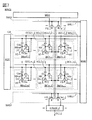
- FIG. 1 is a block diagram showing a configuration example of a semiconductor device.
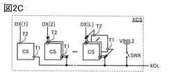
- 2A to 2C are block diagrams showing a configuration example of a circuit included in the semiconductor device.
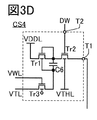
- 3A to 3D are circuit diagrams showing a configuration example of a circuit included in the semiconductor device.
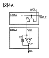
- 4A to 4C are circuit diagrams showing a configuration example of a circuit included in the semiconductor device.
- FIG. 5 is a block diagram showing a configuration example of the semiconductor device.
- FIG. 6 is a timing chart showing an operation example of the semiconductor device.
- FIG. 7 is a block diagram showing a configuration example of the semiconductor device.
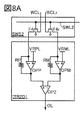
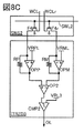
- 8A to 8C are block diagrams showing a configuration example of a circuit included in the semiconductor device.
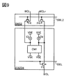
- FIG. 9 is a block diagram showing a configuration example of a circuit included in the semiconductor device.
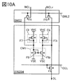
- FIG. 10A is a circuit diagram showing a configuration example of a circuit included in the semiconductor device
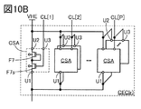
- FIG. 10B is a block diagram showing a configuration example of a circuit included in the semiconductor device
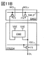
- 11A and 11B are block diagrams showing a configuration example of a circuit included in the semiconductor device
- FIG. 11C is a circuit diagram showing a configuration example of the circuit included in the semiconductor device.
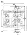
- FIG. 12 is a block diagram showing a configuration example of the semiconductor device.
- 13A and 13B are block diagrams showing a configuration example of a circuit included in the semiconductor device.
- FIG. 14 is a block diagram showing a configuration example of a circuit included in the semiconductor device.
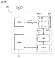
- FIG. 15 is a block diagram showing a configuration example of the olfaction sensor.
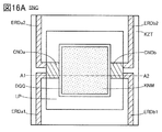
- FIG. 16A is a top view showing an example of a detection element included in the olfaction sensor
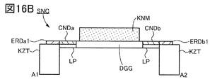
- FIGS. 16B and 16C are cross-sectional views showing an example of the detection element included in the olfaction sensor.
- FIG. 17 is a block diagram showing a configuration example of an electronic device including a pressure sensor or a tactile sensor.
- FIG. 18A is a top view showing an example of a detection element included in the pressure sensor
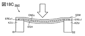
- FIGS. 18B and 18C are cross-sectional views showing an example of the detection element included in the pressure sensor.
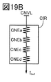
- 19A to 19C are circuit diagrams showing an example of a circuit configuration included in the pressure sensor.
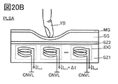
- 20A and 20B are schematic cross-sectional views showing a configuration example of a tactile sensor.
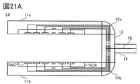
- FIG. 21A to 21C are schematic views showing a configuration example of a hand portion provided in a manipulator or the like.
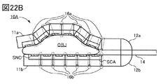
- 22A and 22B are schematic views showing a configuration example of a hand portion provided in a manipulator or the like.
- FIG. 23 is a block diagram showing a configuration example of an electronic device including a taste sensor.
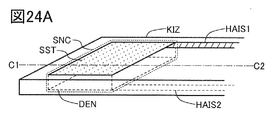
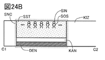
- FIG. 24A is a perspective view showing a configuration example of the taste sensor
- FIG. 24B is a cross-sectional view showing a configuration example of the taste sensor
- FIG. 24C is a block diagram showing a configuration example of a circuit included in an electronic device. is there.
- FIG. 25A is a perspective view showing a configuration example of an electronic device including a taste sensor
- 25B and 25C are perspective views showing a configuration example of a plurality of taste sensors provided in the electronic device.
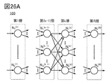
- 26A and 26B are diagrams illustrating a hierarchical neural network.
- FIG. 27 is a block diagram showing a configuration example of the semiconductor device.
- FIG. 28 is a block diagram showing a configuration example of the semiconductor device.
- FIG. 29 is a schematic cross-sectional view showing a configuration example of the semiconductor device.
- FIG. 30 is a schematic cross-sectional view showing a configuration example of the semiconductor device.
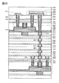
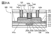
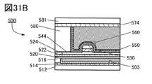
- 31A to 31C are schematic cross-sectional views showing a configuration example of a transistor.
- 32A and 32B are schematic cross-sectional views showing a configuration example of a transistor.
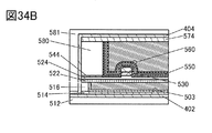
- FIG. 33 is a schematic cross-sectional view showing a configuration example of the semiconductor device.
- FIGS. 36B and 36C are cross-sectional perspective views showing a configuration example of the capacitance element.
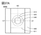
- 37A is a top view showing a configuration example of the capacitance element
- FIG. 37B is a cross-sectional view showing a configuration example of the capacitance
- FIG. 37C is a cross-sectional perspective view showing a configuration example of the capacitance element.
- FIG. 38A is a diagram for explaining the classification of the crystal structure of IGZO, FIG.
- FIG. 38B is a diagram for explaining the XRD spectrum of crystalline IGZO
- FIG. 38C is a diagram for explaining the microelectron diffraction pattern of crystalline IGZO.
- .. 39A is a perspective view showing an example of a semiconductor wafer
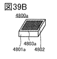
- FIG. 39B is a perspective view showing an example of a chip
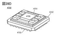
- FIGS. 39C and 39D are perspective views showing an example of an electronic component.
- FIG. 40 is a perspective view showing an example of an electronic device.
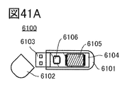
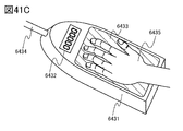
- 41A to 41C are perspective views showing an example of an electronic device.
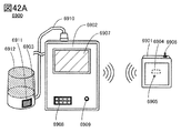
- 42A to 42C are schematic views showing an example of an electronic device.
- FIG. 43 is a circuit diagram illustrating a prototype arithmetic circuit.
- FIG. 43 is a circuit diagram illustrating a prototype arithmetic circuit.
- FIG. 44A is a graph showing the multiplication characteristics of the prototype arithmetic circuit
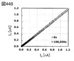
- FIG. 44B is a graph showing the holding characteristics of the prototype arithmetic circuit
- FIG. 45A is a graph showing the multiplication characteristics of the prototype arithmetic circuit by the voltage writing method (Voltage write) and the current writing method (Current writing)
- FIG. 45B shows the voltage writing method (Voltage write) and the current writing method (Current). It is a graph which showed the relationship between the difference of the threshold voltage and the output current in the prototype arithmetic circuit by write).
- 46A and 46B are circuit diagrams illustrating circuits included in the prototype arithmetic circuit.
- FIG. 47A is a graph showing the output characteristics of the current circuit
- FIG. 47B is a graph showing the current INL and DNL output by the current circuit.
- FIG. 48 is a circuit diagram illustrating the conditions for circuit calculation.
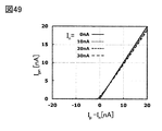
- FIG. 49 is a graph showing the output characteristics of the arithmetic
- the synaptic connection strength can be changed by giving existing information to the neural network.
- the process of giving existing information to the neural network and determining the coupling strength may be called "learning”.
- the process of outputting new information based on the given information and the connection strength may be called “inference” or “cognition”.
- Examples of the neural network model include a Hopfield type and a hierarchical type.
- a neural network having a multi-layer structure may be referred to as a “deep neural network” (DNN), and machine learning by a deep neural network may be referred to as “deep learning”.
- DNN deep neural network
- a metal oxide is a metal oxide in a broad sense. Metal oxides are classified into oxide insulators, oxide conductors (including transparent oxide conductors), oxide semiconductors (also referred to as Oxide Semiconductor or simply OS) and the like. For example, when a metal oxide is used in the active layer of a transistor, the metal oxide may be referred to as an oxide semiconductor. That is, when a metal oxide can form a channel forming region of a transistor having at least one of an amplification action, a rectifying action, and a switching action, the metal oxide is referred to as a metal oxide semiconductor. be able to. Further, when describing as an OS transistor, it can be paraphrased as a transistor having a metal oxide or an oxide semiconductor.
- a metal oxide having nitrogen may also be collectively referred to as a metal oxide. Further, a metal oxide having nitrogen may be referred to as a metal oxynitride.
- the configuration shown in each embodiment can be appropriately combined with the configuration shown in other embodiments to form one aspect of the present invention. Further, when a plurality of configuration examples are shown in one embodiment, the configuration examples can be appropriately combined with each other.
- the content (may be a part of the content) described in one embodiment is the other content (may be a part of the content) described in the embodiment and one or more other implementations. It is possible to apply, combine, or replace at least one content with the content described in the form of (may be a part of the content).
- the figure (which may be a part) described in one embodiment is different from another part of the figure, another figure (which may be a part) described in the embodiment, and one or more other figures.
- the diagram (which may be a part) described in the embodiment By combining at least one diagram with the diagram (which may be a part) described in the embodiment, more diagrams can be constructed.
- FIG. 1 shows a configuration example of an arithmetic circuit that performs a product-sum operation of positive or “0” first data and positive or “0” second data.
- the arithmetic circuit MAC1 shown in FIG. 1 performs a product-sum calculation of the first data corresponding to the potential held in each cell and the input second data, and is activated by using the result of the product-sum calculation. It is a circuit that performs function operations.
- the first data and the second data can be analog data or multi-valued data (discrete data) as an example.
- the arithmetic circuit MAC1 includes a circuit WCS, a circuit XCS, a circuit WSD, a circuit SWS1, a circuit SWS2, a cell array CA, and a conversion circuit ITRZ [1] to a conversion circuit ITRZ [n].
- the cell array CA includes cell IM [1,1] to cell IM [m, n] (m here is an integer of 1 or more, and n here is an integer of 1 or more) and the cell. It has IMref [1] to cell IMref [m]. Each of the cell IM [1,1] to the cell IM [m, n] has a function of holding a potential corresponding to the amount of current according to the first data, and the cell IMref [1] to the cell IMref [m]. Has a function of supplying the potential corresponding to the second data required for performing the product-sum calculation with the held first data to the wiring XCL [1] to the wiring XCL [m].
- the cell array CA in FIG. 1 has n + 1 cells in the row direction and m cells in the column direction arranged in a matrix, whereas the cell array CA has two or more cells in the row direction and one cell in the column direction. As described above, the configuration may be such that they are arranged in a matrix.
- Each of the cell IM [1,1] to the cell IM [m, n] has a transistor F1, a transistor F2, and a capacitance C5 as an example, and each of the cell IMref [1] to the cell IMref [m].
- Each has, as an example, a transistor F1m, a transistor F2m, and a capacitance C5m.
- the size of the transistor F1 included in each of the cell IM [1,1] to the cell IM [m, n] is preferably equal to each other.
- the sizes of the transistors F2 included in each of the cells IM [1,1] to the cells IM [m, n] are equal to each other.
- the size of the transistors F1m included in each of the cells IMref [1] to IMref [m] is preferably equal to each other, and the transistors included in each of the cells IMref [1] to IMref [m].
- the sizes of F2m are equal to each other.
- the sizes of the transistor F1 and the transistor F1m are preferably equal to each other, and the sizes of the transistor F2 and the transistor F2m are preferably equal to each other.
- each transistor By making the transistors equal in size, the electrical characteristics of each transistor can be made almost equal. Therefore, the size of the transistor F1 contained in each of the cell IM [1,1] to the cell IM [m, n] is made equal, and the size of the transistor F1 is made equal to each of the cell IM [1,1] to the cell IM [m, n]. By making the sizes of the included transistors F2 equal, each of the cells IM [1,1] to the cells IM [m, n] can perform substantially the same operation under the same conditions. ..
- the same conditions here include, for example, the input potential of the transistor F1 to the source, drain, gate, etc., the input potential of the transistor F2 to the source, drain, gate, etc., cell IM [1,1] to cell IM [ It refers to the voltage input to each of m and n]. Further, the size of the transistor F1m contained in each of the cell IMref [1] to the cell IMref [m] is made equal, and the size of the transistor F2m contained in each of the cell IMref [1] to the cell IMref [m] is made equal. By making the cells equal, for example, the cells IMref [1] to the cells IMref [m] can make the operation and the result of the operation substantially the same.
- the same conditions include, for example, the input potential of the transistor F1m to the source, drain, gate, etc., the input potential of the transistor F2m to the source, drain, gate, etc., cell IMref [1] to cell IMref [m]. Refers to the voltage etc. input to each of.
- the transistor F1 and the transistor F1m include the case where they finally operate in the linear region when they are in the ON state. That is, it is assumed that each of the gate voltage, the source voltage, and the drain voltage of each of the above-mentioned transistors is in the voltage range operating in the linear region.
- the transistor F1 and the transistor F1m may operate in the saturation region when they are in the ON state, and may operate in the linear region and may operate in the saturation region in a mixed manner.
- the transistor F2 and the transistor F2m are more preferably operated in the subthreshold region (that is, in the transistor F2 or the transistor F2m, when the gate-source voltage is lower than the threshold voltage.
- Shall include (when the drain current increases exponentially with respect to the gate-source voltage). That is, it is assumed that each of the gate voltage, the source voltage, and the drain voltage of each of the above-mentioned transistors is in the voltage range operating in the subthreshold region. Therefore, the transistor F2 and the transistor F2m include the case where the transistor F2 operates so that an off-current flows between the source and the drain.
- the transistor F1 and / or the transistor F1m is preferably an OS transistor as an example.
- the channel forming region of the transistor F1 and / or the transistor F1m is more preferably an oxide containing at least one of indium, gallium, and zinc.
- indium and element M (element M includes, for example, aluminum, gallium, yttrium, copper, vanadium, beryllium, boron, titanium, iron, nickel, germanium, zirconium, molybdenum, lantern, etc.)
- cerium, neodymium, hafnium, tantalum, tungsten, gallium and the like can be mentioned), and oxides containing at least one of zinc may be used. It is more preferable that the transistor F1 and / or the transistor F1m has the structure of the transistor described in the sixth embodiment.
- the leakage current of the transistor F1 and / or the transistor F1m can be suppressed, so that the power consumption of the arithmetic circuit can be reduced.
- the leakage current from the holding node to the writing word line can be made very small, so that the potential refreshing operation of the holding node can be performed. Can be reduced.
- the power consumption of the arithmetic circuit can be reduced.
- the leakage current from the holding node to the wiring WCL or the wiring XCL very small, the cell can hold the potential of the holding node for a long time, so that the calculation accuracy of the calculation circuit can be improved.
- the OS transistor for the transistor F2 and / or the transistor F2m, it is possible to operate in a wide current range in the subthreshold region, so that the current consumption can be reduced.
- the transistor F2 and / or the transistor F2m can also be manufactured at the same time as the transistor F1 and the transistor F1m by using the OS transistor, so that the manufacturing process of the arithmetic circuit may be shortened. ..
- the transistor F2 and / or the transistor F2m can be a transistor (hereinafter, referred to as a Si transistor) containing silicon in the channel forming region other than the OS transistor.
- amorphous silicon sometimes referred to as hydrogenated amorphous silicon
- microcrystalline silicon microcrystalline silicon
- polycrystalline silicon single crystal silicon and the like
- the first terminal of the transistor F1 is electrically connected to the gate of the transistor F2.
- the first terminal of the transistor F2 is electrically connected to the wiring VE.
- the first terminal of the capacitance C5 is electrically connected to the gate of the transistor F2.
- the first terminal of the transistor F1m is electrically connected to the gate of the transistor F2m.
- the first terminal of the transistor F2m is electrically connected to the wiring VE.
- the first terminal having a capacitance of C5 m is electrically connected to the gate of the transistor F2 m.
- a back gate is shown for the transistor F1, the transistor F2, the transistor F1m, and the transistor F2m, and the connection configuration of the back gate is not shown, but the electrical connection destination of the back gate is not shown. It can be decided at the design stage.
- the gate and the back gate may be electrically connected in order to increase the on-current of the transistor. That is, for example, the gate of the transistor F1 and the back gate may be electrically connected, or the gate of the transistor F1m and the back gate may be electrically connected.
- the back gate of the transistor and an external circuit are electrically connected in order to fluctuate the threshold voltage of the transistor or to reduce the off current of the transistor.
- a wiring for connection may be provided, and a potential may be applied to the back gate of the transistor by the external circuit or the like.
- the transistor F1 and the transistor F2 shown in FIG. 1 have a back gate, but the semiconductor device according to one aspect of the present invention is not limited thereto.
- the transistor F1 and the transistor F2 shown in FIG. 1 may have a configuration that does not have a back gate, that is, a transistor having a single gate structure. Further, some transistors may have a back gate, and some other transistors may not have a back gate.
- the transistor F1 and the transistor F2 shown in FIG. 1 are n-channel transistors, but the semiconductor device according to one aspect of the present invention is not limited thereto.
- the transistor F1 and a part or all of the transistor F2 may be replaced with a p-channel type transistor.
- a part or all of the transistor F1 and the transistor F2 are replaced with a p-channel type transistor, it is described in the specification and the like as necessary so that the transistor F1 and the transistor F2 perform the desired operation.
- the voltage given by the wiring, the potential of the node NN, the potential of the node NNref, and the like may be changed.
- the above-mentioned examples of changes regarding the structure and polarity of the transistor are not limited to the transistor F1 and the transistor F2.
- the structure and polarity of the transistors shown in other drawings may be changed.
- the wiring VE is between the first terminal and the second terminal of each transistor F2 of the cell IM [1,1], the cell IM [m, 1], the cell IM [1, n], and the cell IM [m, n]. It is a wiring for passing a current through the cell IMref [1], and also functions as a wiring for passing a current between the first terminal and the second terminal of the respective transistors F2m of the cell IMref [1] and the cell IMref [m].
- the wiring VE functions as a wiring for supplying a constant voltage.
- the constant voltage can be, for example, a low level potential, a ground potential, or the like.
- the second terminal of the transistor F1 is electrically connected to the wiring WCL [1]
- the gate of the transistor F1 is electrically connected to the wiring WSL [1].
- the second terminal of the transistor F2 is electrically connected to the wiring WCL [1]
- the second terminal of the capacitance C5 is electrically connected to the wiring XCL [1].
- the connection point between the first terminal of the transistor F1, the gate of the transistor F2, and the first terminal of the capacitance C5 is a node NN [1,1]. ..
- the second terminal of the transistor F1 is electrically connected to the wiring WCL [1]
- the gate of the transistor F1 is electrically connected to the wiring WSL [m].
- the second terminal of the transistor F2 is electrically connected to the wiring WCL [1]
- the second terminal of the capacitance C5 is electrically connected to the wiring XCL [m].
- the connection point between the first terminal of the transistor F1, the gate of the transistor F2, and the first terminal of the capacitance C5 is a node NN [m, 1]. ..
- the second terminal of the transistor F1 is electrically connected to the wiring WCL [n]
- the gate of the transistor F1 is electrically connected to the wiring WSL [1].
- the second terminal of the transistor F2 is electrically connected to the wiring WCL [n]
- the second terminal of the capacitance C5 is electrically connected to the wiring XCL [1].
- the connection point between the first terminal of the transistor F1, the gate of the transistor F2, and the first terminal of the capacitance C5 is a node NN [1, n]. ..
- the second terminal of the transistor F1 is electrically connected to the wiring WCL [n]
- the gate of the transistor F1 is electrically connected to the wiring WSL [m].
- the second terminal of the transistor F2 is electrically connected to the wiring WCL [n]
- the second terminal of the capacitance C5 is electrically connected to the wiring XCL [m].
- the connection point between the first terminal of the transistor F1, the gate of the transistor F2, and the first terminal of the capacitance C5 is a node NN [m, n]. ..
- the second terminal of the transistor F1m is electrically connected to the wiring XCL [1]
- the gate of the transistor F1m is electrically connected to the wiring WSL [1].
- the second terminal of the transistor F2m is electrically connected to the wiring XCL [1]
- the second terminal of the capacitance C5 is electrically connected to the wiring XCL [1].
- the connection point between the first terminal of the transistor F1m, the gate of the transistor F2m, and the first terminal of the capacitance C5 is a node NNref [1].
- the second terminal of the transistor F1m is electrically connected to the wiring XCL [m]
- the gate of the transistor F1m is electrically connected to the wiring WSL [m].
- the second terminal of the transistor F2m is electrically connected to the wiring XCL [m]
- the second terminal of the capacitance C5 is electrically connected to the wiring XCL [m].
- the connection point between the first terminal of the transistor F1m, the gate of the transistor F2m, and the first terminal of the capacitance C5 is a node NNref [m].
- node NN [1,1] to the node NN [m, n] and the node NNref [1] to the node NNref [m] function as holding nodes of their respective cells.
- the transistor F2 has a diode connection configuration.
- the constant voltage given by the wiring VE as the ground potential (GND) when the transistor F1 is in the ON state and the current of the current amount I flows from the wiring WCL to the second terminal of the transistor F2, the gate (node NN) of the transistor F2.
- the potential of is determined according to the amount of current I. Since the transistor F1 is in the ON state, the potential of the second terminal of the transistor F2 is ideally equal to the gate (node NN) of the transistor F2.
- the transistor F2 can pass a current having a current amount I corresponding to the ground potential of the first terminal of the transistor F2 and the potential of the gate (node NN) of the transistor F2 between the source and drain of the transistor F2.
- such an operation is referred to as "setting (programming) the amount of current flowing between the source and drain of the transistor F2 of the cell IM to I" and the like.
- the circuit SWS1 has a transistor F3 [1] to a transistor F3 [n] as an example.
- the first terminal of the transistor F3 [1] is electrically connected to the wiring WCL [1]
- the second terminal of the transistor F3 [1] is electrically connected to the circuit WCS, and the gate of the transistor F3 [1].
- the first terminal of the transistor F3 [n] is electrically connected to the wiring WCL [n]
- the second terminal of the transistor F3 [n] is electrically connected to the circuit WCS, and the gate of the transistor F3 [n]. Is electrically connected to the wiring SWL1.
- each of the transistors F3 [1] to F3 [n] for example, a transistor applicable to the transistor F1 and / or the transistor F2 can be used. In particular, it is preferable to use an OS transistor as each of the transistors F3 [1] to F3 [n].
- the circuit SWS1 functions as a circuit that puts a conductive state or a non-conducting state between the circuit WCS and each of the wiring WCL [1] to the wiring WCL [n].
- the circuit SWS2 has a transistor F4 [1] to a transistor F4 [n] as an example.
- the first terminal of the transistor F4 [1] is electrically connected to the wiring WCL [1]
- the second terminal of the transistor F4 [1] is electrically connected to the input terminal of the conversion circuit ITRZ [1].
- the gate of the transistor F4 [1] is electrically connected to the wiring SWL2.
- the first terminal of the transistor F4 [n] is electrically connected to the wiring WCL [n]
- the second terminal of the transistor F4 [n] is electrically connected to the input terminal of the conversion circuit ITRZ [n].
- the gate of the transistor F4 [n] is electrically connected to the wiring SWL2.
- each of the transistors F4 [1] to F4 [n] for example, a transistor applicable to the transistor F1 and / or the transistor F2 can be used. In particular, it is preferable to use an OS transistor as each of the transistors F4 [1] to F4 [n].
- the circuit SWS2 has a function of setting a conductive state or a non-conducting state between the wiring WCL [1] and the conversion circuit ITRZ [1] and between the wiring WCL [n] and the conversion circuit ITRZ [n].
- the circuit WCS has a function of supplying data to be stored in each cell of the cell array CA.
- the circuit XCS is electrically connected to the wiring XCL [1] to the wiring XCL [m].
- the circuit XCS has a function of passing a current amount corresponding to the reference data described later or a current amount corresponding to the second data to each of the cell IMref [1] to the cell IMref [m] of the cell array CA.
- the circuit WSD is electrically connected to the wiring WSL [1] to the wiring WSL [m].
- the circuit WSD supplies a predetermined signal to the wiring WSL [1] to the wiring WSL [m] when writing the first data to the cell IM [1,1] to the cell IM [m, n]. 1 It has a function of selecting a row of the cell array CA to write data to. That is, the wiring WSL [1] to the wiring WSL [m] function as a writing word line.
- the circuit WSD is electrically connected to the wiring SWL1 and the wiring SWL2 as an example.
- the circuit WSD has a function of making a predetermined signal between the circuit WCS and the cell array CA in a conductive state or a non-conducting state by supplying a predetermined signal to the wiring SWL1, and a conversion circuit by supplying a predetermined signal to the wiring SWL2. It has a function of making the ITRZ [1] to the conversion circuit ITRZ [n] and the cell array CA in a conductive state or a non-conducting state.
- Each of the conversion circuit ITRZ [1] and the conversion circuit ITRZ [n] has an input terminal and an output terminal as an example.
- the output terminal of the conversion circuit ITRZ [1] is electrically connected to the wiring OL [1]
- the output terminal of the conversion circuit ITRZ [n] is electrically connected to the wiring OL [n].
- Each of the conversion circuit ITRZ [1] and the conversion circuit ITRZ [n] has a function of inputting a current to the input terminal, converting the voltage into a voltage corresponding to the amount of the current, and outputting the voltage from the output terminal.
- the voltage may be, for example, an analog voltage, a digital voltage, or the like.
- each of the conversion circuit ITRZ [1] to the conversion circuit ITRZ [n] may have a function-based arithmetic circuit. In this case, for example, the converted voltage may be used to perform a function calculation by the calculation circuit, and the result of the calculation may be output to the wiring OL [1] to the wiring OL [n].
- a sigmoid function for example, a tanh function, a softmax function, a ReLU function, a threshold function, etc.
- a sigmoid function for example, a sigmoid function, a tanh function, a softmax function, a ReLU function, a threshold function, etc.
- a sigmoid function for example, a sigmoid function, a tanh function, a softmax function, a ReLU function, a threshold function, etc.
- Circuit WCS Circuit XCS
- circuit WCS Circuit XCS
- FIG. 2A is a block diagram showing an example of the circuit WCS. Note that FIG. 2A also shows the circuit SWS1, the transistor F3, the wiring SWL1, and the wiring WCL in order to show the electrical connection with the circuits around the circuit WCS. Further, the transistor F3 is any one of the transistor F3 [1] to the transistor F3 [n] included in the arithmetic circuit MAC1 of FIG. 1, and the wiring WCL is included in the arithmetic circuit MAC1 of FIG. It is any one of the wiring WCL [1] and the wiring WCL [n].
- the circuit WCS shown in FIG. 2A has a switch SWW as an example.
- the first terminal of the switch SWW is electrically connected to the second terminal of the transistor F3, and the second terminal of the switch SWW is electrically connected to the wiring VINIL1.
- the wiring VINIL1 functions as a wiring that gives a potential for initialization to the wiring WCL, and the potential for initialization can be a ground potential (GND), a low level potential, a high level potential, or the like.
- the switch SWW is turned on only when a potential for initialization is applied to the wiring WCL, and is turned off at other times.
- the switch SWW for example, an electric switch such as an analog switch or a transistor can be applied.
- the transistor can be a transistor having the same structure as the transistor F1 and the transistor F2.
- a mechanical switch may be applied.
- the circuit WCS of FIG. 2A has a plurality of current source CSs as an example.
- the circuit WCS has a function of outputting the first data of K bits (2 K value) (K is an integer of 1 or more) as a current amount, and in this case, the circuit WCS has 2 K- 1 pieces.
- the circuit WCS has one current source CS that outputs information corresponding to the value of the first bit as a current, and has two current source CSs that output information corresponding to the value of the second bit as a current. It also has 2K-1 current sources CS that output information corresponding to the K-bit value as a current.
- each current source CS has a terminal T1 and a terminal T2.
- the terminal T1 of each current source CS is electrically connected to the second terminal of the transistor F3 included in the circuit SWS1.
- the terminal T2 of the one current source CS is electrically connected to the wiring DW [1]
- each of the terminals T2 of the two current sources CS is electrically connected to the wiring DW [2], 2 K -1
- Each of the terminals T2 of the current source CS is electrically connected to the wiring DW [K].
- Each of the plurality of current source CSs included in the circuit WCS has a function of outputting the same constant current I Wut from the terminal T1.
- the error of the constant current I Wut output from each of the terminals T1 of the plurality of current sources CS is preferably within 10%, more preferably within 5%, and even more preferably within 1%. In the present embodiment, it is assumed that there is no error in the constant current I Wut output from the terminals T1 of the plurality of current sources CS included in the circuit WCS.
- the wiring DW [1] to the wiring DW [K] function as wiring for transmitting a control signal for outputting a constant current I Wut from the electrically connected current source CS.
- the current source CS electrically connected to the wiring DW [1] uses I Wut as a constant current of the transistor F3.
- the current source CS electrically connected to the wiring DW [1] does not output I Wut .
- the two current sources CS electrically connected to the wiring DW [2] when a high level potential is applied to the wiring DW [2], the two current sources CS electrically connected to the wiring DW [2] generate a constant current of a total of 2I Wut in the transistor F3.
- the current source CS electrically connected to the wiring DW [2] draws a total constant current of 2I Wut. Do not output.
- the current flowing through one current source CS electrically connected to the wiring DW [1] corresponds to the value of the first bit
- the two currents electrically connected to the wiring DW [2] corresponds to the value of the second bit
- the amount of current flowing through the K current source CS electrically connected to the wiring DW [K] corresponds to the value of the K bit.
- I Wut flows from the circuit WCS to the second terminal of the transistor F3 of the circuit SWS1 as a constant current. Further, for example, when the value of the first bit is "0" and the value of the second bit is "1", a low level potential is given to the wiring DW [1] and a high level potential is given to the wiring DW [2]. Is given. At this time, 2I Wut flows from the circuit WCS to the second terminal of the transistor F3 of the circuit SWS1 as a constant current. Further, for example, when the value of the first bit is "1" and the value of the second bit is "1", a high level potential is given to the wiring DW [1] and the wiring DW [2].
- 3I Wut flows from the circuit WCS to the second terminal of the transistor F3 of the circuit SWS1 as a constant current. Further, for example, when the value of the first bit is "0" and the value of the second bit is "0", a low level potential is given to the wiring DW [1] and the wiring DW [2]. At this time, a constant current does not flow from the circuit WCS to the second terminal of the transistor F3 of the circuit SWS1.
- FIG. 2A illustrates the circuit WCS when K is an integer of 3 or more, but when K is 1, the circuit WCS of FIG. 2A is connected to the wiring DW [2] to the wiring DW [K].
- the current source CS that is electrically connected to the device may not be provided.
- the circuit WCS of FIG. 2A may be configured so as not to provide the current source CS electrically connected to the wiring DW [3] to the wiring DW [K].
- the current source CS1 shown in FIG. 3A is a circuit applicable to the current source CS included in the circuit WCS of FIG. 2A, and the current source CS1 includes a transistor Tr1 and a transistor Tr2.
- the first terminal of the transistor Tr1 is electrically connected to the wiring VDDL, and the second terminal of the transistor Tr1 is electrically connected to the gate of the transistor Tr1, the back gate of the transistor Tr1, and the first terminal of the transistor Tr2. It is connected.
- the second terminal of the transistor Tr2 is electrically connected to the terminal T1, and the gate of the transistor Tr2 is electrically connected to the terminal T2. Further, the terminal T2 is electrically connected to the wiring DW.
- the wiring DW is any one of the wiring DW [1] to the wiring DW [n] in FIG. 2A.
- Wiring VDDL functions as wiring that gives a constant voltage.
- the constant voltage can be, for example, a high level potential.
- the constant voltage given by the wiring VDDL is set to a high level potential
- a high level potential is input to the first terminal of the transistor Tr1.
- the potential of the second terminal of the transistor Tr1 is set to a potential lower than the high level potential.
- the first terminal of the transistor Tr1 functions as a drain
- the second terminal of the transistor Tr1 functions as a source.
- the gate-source voltage of the transistor Tr1 becomes 0V. Therefore, when the threshold voltage of the transistor Tr1 is within an appropriate range, a current (drain current) in the current range of the subthreshold region flows between the first terminal and the second terminal of the transistor Tr1.
- the amount of the current is preferably 1.0 ⁇ 10-8 A or less, and more preferably 1.0 ⁇ 10-12 A or less. Further, it is more preferably 1.0 ⁇ 10 -15 A or less. Further, for example, it is more preferable that the current is in a range where the current increases exponentially with respect to the gate-source voltage. That is, the transistor Tr1 functions as a current source for passing a current in the current range when operating in the subthreshold region. Note that the current is equivalent to I Wut, or later to I Xut described above.
- the transistor Tr2 functions as a switching element.
- the first terminal of the transistor Tr2 functions as a drain and the second terminal of the transistor Tr2 functions as a source.
- the back gate of the transistor Tr2 and the second terminal of the transistor Tr2 are electrically connected, the voltage between the back gate and the source becomes 0 V. Therefore, when the threshold voltage of the transistor Tr2 is within an appropriate range, the transistor Tr2 is turned on by inputting a high level potential to the gate of the transistor Tr2, and the gate of the transistor Tr2 is low. When the level potential is input, the transistor Tr2 is turned off.
- the transistor Tr2 when the transistor Tr2 is in the ON state, the current in the current range of the subthreshold region described above flows from the second terminal of the transistor Tr1 to the terminal T1, and when the transistor Tr2 is in the Off state, the current is the transistor Tr1. It is assumed that the current does not flow from the second terminal to the terminal T1.
- the circuit applicable to the current source CS included in the circuit WCS of FIG. 2A is not limited to the current source CS1 of FIG. 3A.
- the current source CS1 has a configuration in which the back gate of the transistor Tr2 and the second terminal of the transistor Tr2 are electrically connected, but the back gate of the transistor Tr2 is electrically connected to another wiring. It may be configured as such.
- An example of such a configuration is shown in FIG. 3B.
- the current source CS2 shown in FIG. 3B has a configuration in which the back gate of the transistor Tr2 is electrically connected to the wiring VTHL.
- the current source CS2 when the wiring VTHL is electrically connected to an external circuit or the like, a predetermined potential is given to the wiring VTHL by the external circuit or the like, and the predetermined potential is given to the back gate of the transistor Tr2. it can. As a result, the threshold voltage of the transistor Tr2 can be changed. In particular, the off-current of the transistor Tr2 can be reduced by increasing the threshold voltage of the transistor Tr2.
- the current source CS1 has a configuration in which the back gate of the transistor Tr1 and the second terminal of the transistor Tr1 are electrically connected, but between the back gate of the transistor Tr2 and the second terminal.
- the voltage may be held by the capacity.
- FIG. 3C An example of such a configuration is shown in FIG. 3C.
- the current source CS3 shown in FIG. 3C has a transistor Tr3 and a capacitance C6 in addition to the transistor Tr1 and the transistor Tr2.
- the point where the second terminal of the transistor Tr1 and the back gate of the transistor Tr1 are electrically connected via the capacitance C6, and the back gate of the transistor Tr1 and the first terminal of the transistor Tr3 are electrically connected.
- the current source CS3 differs from the current source CS1 in that it is connected to the wiring VWL, and the second terminal of the transistor Tr3 is electrically connected to the wiring VTL, and the gate of the transistor Tr3 is electrically connected to the wiring VWL. It is configured to be.
- the current source CS3 can make the wiring VTL and the back gate of the transistor Tr1 conductive by applying a high level potential to the wiring VWL to turn on the transistor Tr3. At this time, a predetermined potential can be input from the wiring VTL to the back gate of the transistor Tr1. Then, by applying a low level potential to the wiring VWL to turn off the transistor Tr3, the voltage between the second terminal of the transistor Tr1 and the back gate of the transistor Tr1 can be maintained by the capacitance C6. That is, the threshold voltage of the transistor Tr1 can be changed by determining the voltage applied to the back gate of the transistor Tr1 by the wiring VTL, and the threshold voltage of the transistor Tr1 is fixed by the transistor Tr3 and the capacitance C6. can do.
- the circuit applicable to the current source CS included in the circuit WCS of FIG. 2A may be the current source CS4 shown in FIG. 3D.
- the current source CS4 has a configuration in which the back gate of the transistor Tr2 is electrically connected to the wiring VTHL instead of the second terminal of the transistor Tr2 in the current source CS3 of FIG. 3C. That is, the current source CS4 can change the threshold voltage of the transistor Tr2 according to the potential given by the wiring VTHL, similarly to the current source CS2 of FIG. 3B.
- the current source CS4 applies a high level potential to the wiring VTHL, lowers the threshold voltage of the transistor Tr2, and raises the on-current of the transistor Tr2, thereby increasing the on-current of the transistor Tr1.
- a large current flowing between the terminals can be passed from the terminal T1 to the outside of the current source CS4.
- the circuit WCS outputs a current corresponding to the first data of K bits. can do.
- the amount of the current can be, for example, the amount of current flowing between the first terminal and the second terminal within the range in which the transistor F1 operates in the subthreshold region.
- the circuit WCS of FIG. 2B has a configuration in which one current source CS of FIG. 3A is connected to each of the wiring DW [1] to the wiring DW [K]. Further, when the channel width of the transistor Tr1 [1] is w [1], the channel width of the transistor Tr1 [2] is w [2], and the channel width of the transistor Tr1 [K] is w [K], each channel is used.
- the circuit WCS shown in FIG. 2B corresponds to the first data of K bits like the circuit WCS of FIG. 2A. It can output current.
- the transistor Tr1 (including the transistor Tr1 [1] to the transistor Tr2 [K]), the transistor Tr2 (including the transistor Tr2 [1] to the transistor Tr2 [K]), and the transistor Tr3 are, for example, the transistor F1 and / Alternatively, a transistor applicable to the transistor F2 can be used.
- an OS transistor may be used as the transistor Tr1 (including the transistor Tr1 [1] to the transistor Tr2 [K]), the transistor Tr2 (including the transistor Tr2 [1] to the transistor Tr2 [K]), and the transistor Tr3. preferable.
- FIG. 2C is a block diagram showing an example of the circuit XCS. Note that FIG. 2C also shows the wiring XCL in order to show the electrical connection with the circuits around the circuit WCS. Further, the wiring XCL is any one of the wiring XCL [1] and the wiring XCL [m] included in the arithmetic circuit MAC1 of FIG.
- the circuit XCS shown in FIG. 2C has a switch SWX as an example.
- the first terminal of the switch SWX is electrically connected to the wiring XCL and the plurality of current sources CS, and the second terminal of the switch SWX is electrically connected to the wiring VINIL2.
- the wiring VINIL 2 functions as a wiring that gives a potential for initialization to the wiring XCL, and the potential for initialization can be a ground potential (GND), a low level potential, a high level potential, or the like.
- the initialization potential given by the wiring VINIL2 may be equal to the potential given by the wiring VINIL1.
- the switch SWX is turned on only when a potential for initialization is applied to the wiring XCL, and is turned off at other times.
- the switch SWX can be, for example, a switch applicable to the switch SWW.
- the circuit configuration of the circuit XCS of FIG. 2C can be substantially the same as that of the circuit WCS of FIG. 3A.
- the circuit XCS has a function of outputting reference data as a current amount and a function of outputting second data of L bits (2 L value) (L is an integer of 1 or more) as a current amount.
- the circuit XCS has 2 L- 1 current source CS.
- the circuit XCS has one current source CS that outputs information corresponding to the value of the first bit as a current, and has two current source CSs that output information corresponding to the value of the second bit as a current.
- it has 2 L-1 current sources CS that output information corresponding to the value of the L-th bit as a current.
- the value of the first bit can be "1" and the value of the second and subsequent bits can be "0".
- the terminal T2 of one current source CS is electrically connected to the wiring DX [1], and each of the terminals T2 of the two current source CS is electrically connected to the wiring DX [2].
- 2 L-1 Each of the terminals T2 of the current source CS is electrically connected to the wiring DX [L].
- Each of the plurality of current source CSs included in the circuit XCS has a function of outputting IXut from the terminal T1 as the same constant current.
- the wiring DX [1] to the wiring DX [L] function as wiring for transmitting a control signal for outputting the IXut from the electrically connected current source CS. That is, the circuit XCS has a function of passing an amount of current corresponding to the information of the L bits sent from the wiring DX [1] to the wiring DX [L] to the wiring XCL.
- 2I Xut flows from the circuit XCS to the wiring XCL as a constant current.
- 3I Xut flows from the circuit XCS to the wiring XCL as a constant current.
- a low level potential is given to the wiring DX [1] and the wiring DX [2].
- no constant current flows from the circuit XCS to the wiring XCL.
- a current having a current amount of 0 flows from the circuit XCS to the wiring XCL.
- the current amount 0, I Xut , 2I Xut , 3I Xut, etc. output by the circuit XCS can be used as the second data output by the circuit XCS, and in particular, the current amount I Xut output by the circuit XCS is a circuit. It can be reference data output by XCS.
- the constant current I Xut output from each of the terminals T1 of the plurality of current source CSs is preferably within 10%, more preferably within 5%, and even more preferably within 1%. In this embodiment, it is assumed that there is no error in the constant current I Xut output from the terminals T1 of the plurality of current sources CS included in the circuit XCS.
- any one of the current sources CS1 to CS4 of FIGS. 3A to 3D can be applied as in the current source CS of the circuit WCS.
- the wiring DW shown in FIGS. 3A to 3D may be replaced with the wiring DX.
- the circuit XCS can pass a current in the current range of the subthreshold region through the wiring XCL as reference data or second data of the L bit.
- the same circuit configuration as the circuit WCS shown in FIG. 2B can be applied.
- the circuit WCS shown in FIG. 2B is replaced with the circuit XCS
- the wiring DW [1] is replaced with the wiring DX [1]
- the wiring DW [2] is replaced with the wiring DX [2]
- the wiring DW [K] is wired. It may be considered by replacing with DX [L], replacing the switch SWW with the switch SWX, and replacing the wiring VINIL1 with the wiring VINIL2.
- the conversion circuit ITRZ1 shown in FIG. 4A is an example of a circuit applicable to the conversion circuit ITRZ [1] to the conversion circuit ITRZ [n] of FIG.
- FIG. 4A also shows the circuit SWS2, the wiring WCL, the wiring SWL2, and the transistor F4 in order to show the electrical connection with the circuits around the conversion circuit ITRZ1.
- the wiring WCL is any one of the wiring WCL [1] and the wiring WCL [n] included in the arithmetic circuit MAC1 of FIG. 1
- the transistor F4 is included in the arithmetic circuit MAC1 of FIG. It is any one of the transistor F4 [1] to the transistor F4 [n].
- the conversion circuit ITRZ1 of FIG. 4A is electrically connected to the wiring WCL via the transistor F4. Further, the conversion circuit ITRZ1 is electrically connected to the wiring OL.
- the conversion circuit ITRZ1 has a function of converting the amount of current flowing from the conversion circuit ITRZ1 to the wiring WCL or the amount of current flowing from the wiring WCL to the conversion circuit ITRZ1 into an analog voltage and outputting the analog voltage to the wiring OL. That is, the conversion circuit ITRZ1 has a current-voltage conversion circuit.
- the conversion circuit ITRZ1 of FIG. 4A has a resistor R5 and an operational amplifier OP1 as an example.
- the inverting input terminal of the operational amplifier OP1 is electrically connected to the first terminal of the resistor R5 and the second terminal of the transistor F4.
- the non-inverting input terminal of the operational amplifier OP1 is electrically connected to the wiring VRL.
- the output terminal of the operational amplifier OP1 is electrically connected to the second terminal of the resistor R5 and the wiring OL.
- Wiring VRL functions as wiring that gives a constant voltage.
- the constant voltage can be, for example, a ground potential (GND), a low level potential, or the like.
- the conversion circuit ITRZ1 has the configuration shown in FIG. 4A, so that the amount of current flowing from the wiring WCL to the conversion circuit ITRZ1 via the transistor F4, or the current flowing from the conversion circuit ITRZ1 to the wiring WCL via the transistor F4.
- the amount can be converted into an analog voltage and output to the wiring OL.
- the inverting input terminal of the operational amplifier OP1 becomes virtual ground, so the analog voltage output to the wiring OL is based on the ground potential (GND). It can be a voltage.
- the conversion circuit ITRZ1 of FIG. 4A is configured to output an analog voltage, but the circuit configuration applicable to the conversion circuit ITRZ [1] to the conversion circuit ITRZ [n] of FIG. 1 is not limited to this.
- the conversion circuit ITRZ1 may have a configuration having an analog-digital conversion circuit ADC as shown in FIG. 4B.
- the input terminal of the analog-digital conversion circuit ADC is electrically connected to the output terminal of the operational amplifier OP1 and the second terminal of the resistor R5, and the analog-digital conversion circuit ADC has.
- the output terminal is electrically connected to the wiring OL.
- the conversion circuit ITRZ2 of FIG. 4B can output a digital signal to the wiring OL.
- the conversion circuit ITRZ2 when the digital signal output to the wiring OL is 1 bit (binary value), the conversion circuit ITRZ2 may be replaced with the conversion circuit ITRZ3 shown in FIG. 4C.
- the conversion circuit ITRZ3 of FIG. 4C has a configuration in which the comparator CMP1 is provided in the conversion circuit ITRZ1 of FIG. 4A. Specifically, in the conversion circuit ITRZ3, the first input terminal of the comparator CMP1 is electrically connected to the output terminal of the operational amplifier OP1 and the second terminal of the resistor R5, and the second input terminal of the comparator CMP1 is the wiring VRL2. The output terminal of the comparator CMP1 is electrically connected to the wiring OL.
- the wiring VRL2 functions as a wiring that gives a potential for comparison with the potential of the first terminal of the comparator CMP1.
- the conversion circuit ITRZ3 of FIG. 4C has a magnitude of the voltage converted from the amount of current flowing between the source and drain of the transistor F4 by the current-voltage conversion circuit and the voltage given by the wiring VRL2.
- a low level potential or a high level potential can be output to the wiring OL according to the above.
- the conversion circuit ITRZ [1] to the conversion circuit ITRZ [n] applicable to the arithmetic circuit MAC1 of FIG. 1 is not limited to the conversion circuits ITRZ1 to the conversion circuit ITRZ3 shown in FIGS. 4A to 4C, respectively.
- the conversion circuit ITRZ1 to the conversion circuit ITRZ3 have a functional arithmetic circuit.
- the arithmetic circuit of the function system can be an arithmetic circuit such as a sigmoid function, a tanh function, a softmax function, a ReLU function, or a threshold function.
- the operation circuit MAC1 can change the circuit configuration depending on the situation.
- the arithmetic circuit MAC1 may be changed to a configuration in which the circuit SWS1 is not provided, as shown in the arithmetic circuit MAC1A shown in FIG.
- the circuit SWS1 can stop the current flowing from the circuit WCS to the wiring WCL [1] to the wiring WCL [n], but in the case of the arithmetic circuit MAC1A, the circuit WCS can stop the current flowing from the circuit WCS to the wiring WCL.
- the current flowing through [1] to the wiring WCL [n] may be stopped.
- the circuit WCS of FIG. 2A is applied as the circuit WCS included in the arithmetic circuit MAC1A and the current source CS1 of FIG. 3A is applied as the current source CS, the wiring DW [1] to the wiring DW [K] ], A low level potential may be input and the switch SWW may be turned off.
- the circuit WCS in this way, the current flowing from the circuit WCS to the wiring WCL [1] to the wiring WCL [n] can be stopped.
- the calculation can be performed using the calculation circuit MAC1A instead of the calculation circuit MAC1.
- FIG. 6 shows a timing chart of an operation example of the arithmetic circuit MAC1.
- the timing chart of FIG. 6 shows the wiring SWL1, the wiring SWL2, the wiring WSL [i] (i is an integer of 1 or more and m-1 or less), and the wiring between the time T11 and the time T23 and in the vicinity thereof.
- the cell IM [i, j] the first terminal of the transistor F2 contained in the - amount of the current flowing between the second terminal I F2 [i, j] and the cell IMref [i ],
- the current amount I F2 [i + 1, j ] that flows between the cells IMref first terminal of the transistor F2m contained in [i + 1] - current amount I F2m flowing between the second terminal [i + 1], each variation in Is also shown.
- circuit WCS of FIG. 2A is applied as the circuit WCS of the arithmetic circuit MAC1
- the circuit XCS of FIG. 2C is applied as the circuit XCS of the arithmetic circuit MAC1.
- the potential of the wiring VE is the ground potential GND.
- the potentials of the node NN [i, j], the node NN [i + 1, j], the node NNref [i], and the node NNref [i + 1] are set to the ground potential GND as initial settings. It is assumed that Specifically, for example, the potential for initialization of the wiring VINIL1 in FIG. 2A is set to the ground potential GND, and is included in the switch SWW, the transistor F3, and the cell IM [i, j] and the cell IM [i + 1, j].
- the potentials of the nodes NN [i, j] and the nodes NN [i + 1, j] can be set to the ground potential GND.
- the potential for initialization of the wiring VINIL2 in FIG. 2C is set to the ground potential GND, and the switch SWX and the respective transistors F1m included in the cell IMref [i, j] and the cell IMref [i + 1, j] are used.
- the potentials of the nodes NNref [i, j] and the nodes NNref [i + 1, j] can be set to the ground potential GND.
- a high level potential (denoted as High in FIG. 6) is applied to the wiring SWL1 and a low level potential (denoted as Low in FIG. 6) is applied to the wiring SWL2.
- a high level potential is applied to each gate of the transistor F3 [1] to the transistor F3 [n]
- each of the transistor F3 [1] to the transistor F3 [n] is turned on
- the transistor F4 [1] is turned on.
- a low level potential is applied to each gate of the transistor F4 [n], and each of the transistor F4 [1] to the transistor F4 [n] is turned off.
- a low level potential is applied to the wiring WSL [i] and the wiring WSL [i + 1].
- the gate of the transistor F1 included in the cell IM [i, 1] to the cell IM [i, n] of the i-th row of the cell array CA and the gate of the transistor F1m included in the cell IMref [i] A low level potential is applied to and, and the respective transistors F1 and F1m are turned off.
- a low level potential is applied to the, and the respective transistors F1 and F1m are turned off.
- the ground potential GND is applied to the wiring XCL [i] and the wiring XCL [i + 1].
- the potential for initializing the wiring VINIL2 is set to the ground potential GND, and the switch SWX is set.
- the potentials of the wiring XCL [i] and the wiring XCL [i + 1] can be set to the ground potential GND.
- the wiring WCL shown in FIG. 2A is the wiring WCL [1] to the wiring WCL [K]
- the wiring DW [1] to the wiring DW [K] No first data has been input.
- the wiring XCL shown in FIG. 2C is each of the wiring XCL [1] to the wiring XCL [K]
- the second data is not input to the wiring DX [1] to the wiring DX [L].
- a low level potential is input to each of the wiring DW [1] to the wiring DW [K] in the circuit WCS of FIG. 2A, and the wiring DX [1] in the circuit XCS of FIG. 2C. It is assumed that a low level potential is input to each of the wiring DX [L].
- a low level potential is applied to the wiring WSL [1] to the wiring WSL [m] excluding the wiring WSL [i], and the cells other than the i-th row of the cell array CA
- the transistor F1 included in the IM [1,1] to the cell IM [m, n] and the transistor F1m included in the cell IMref [1] to the cell IMref [m] other than the i-th row are in the off state. It is assumed that it is.
- ground potential GND has been continuously applied to the wiring XCL [1] to the wiring XCL [m] from before the time T12.
- a current of a current amount I 0 [i, j] flows from the circuit WCS to the cell array CA via the transistor F3 [j] as the first data.
- the wiring WCL shown in FIG. 2A is the wiring WCL [j]
- a signal corresponding to the first data is input to each of the wiring DW [1] to the wiring DW [K].
- Current I 0 [i, j] flows from the circuit WCS to the second terminal of the transistor F3 [j].
- the first terminal of the transistor F1 included in the cell IM [i, j] in the i-th row of the cell array CA and the wiring WCL [j] are in a conductive state.
- the transistor F1 included in the cell IM [i, j] when the transistor F1 included in the cell IM [i, j] is turned on, the transistor F2 included in the cell IM [i, j] has a diode connection configuration. Therefore, when a current flows from the wiring WCL [j] to the cell IM [i, j], the potentials of the gate of the transistor F2 and the second terminal of the transistor F2 become substantially equal. The potential is determined by the amount of current flowing from the wiring WCL [j] to the cell IM [i, j], the potential of the first terminal of the transistor F2 (here, GND), and the like.
- the potential of the gate (node NN [i, j]) of the transistor F2 is caused by the current of the current amount I 0 [i, j] flowing from the wiring WCL [j] to the cell IM [i, j].
- the threshold voltage of the transistor F2 is Vth [i, j]
- the amount of current I 0 [i, j] when the transistor F2 operates in the subthreshold region is described by the following equation. it can.
- I a is the drain current when V g [i, j] is V th [i, j], and J is a correction coefficient determined by the temperature, device structure, and the like.
- the circuit XCS, the wiring XCL [i], the current of the current amount I ref0 flows as reference data.
- the wiring XCL shown in FIG. 2C is the wiring XCL [i]
- the wiring DX [1] has a high level potential
- the wiring DX [2] to the wiring DX [K] have a low level potential.
- Is input, and the current I ref0 flows from the circuit XCS to the wiring XCL [i]. That is, I ref0 I Xut .
- the transistor F2m included in the cell IMref [i] has a diode connection configuration. .. Therefore, when a current flows from the wiring XCL [i] to the cell IMref [i], the potentials of the gate of the transistor F2m and the second terminal of the transistor F2m become substantially equal. The potential is determined by the amount of current flowing from the wiring XCL [i] to the cell IMref [i], the potential of the first terminal of the transistor F2m (here, GND), and the like.
- the gate of the transistor F2 (node NNref [i]) is assumed to be V gm [i]
- the potential of the wiring XCL [i] at this time is also set to V gm [i]. That is, in the transistor F2m, the gate-source voltage becomes V gm [i] -GND, and the current amount I ref 0 is set as the current flowing between the first terminal and the second terminal of the transistor F2m.
- the current amount I ref0 when transistor F2m operates in the subthreshold region can be described as the following equation.
- the correction coefficient J is the same as that of the transistor F2 included in the cell IM [i, j].
- the device structure and size (channel length, channel width) of the transistors are the same.
- the correction coefficient J of each transistor varies due to manufacturing variation, it is assumed that the variation is suppressed to the extent that the discussion described later holds with practically sufficient accuracy.
- the weighting coefficient w [i, j], which is the first data is defined as follows.
- equation (1.1) can be rewritten as the following equation.
- the capacitance C5 has the potential of the gate (node NN [i, j]) of the transistor F2 and the wiring XCL [i]. The difference between the potential and V g [i, j] -V gm [i] is retained. Further, when the transistor F1 included in the cell IMref [i] is turned off, the potential of the gate (node NNref [i]) of the transistor F2m and the potential of the wiring XCL [i] are added to the capacitance C5m. The difference between, and 0 is retained.
- the voltage held by the capacitance C5m may be a voltage that is not 0 (here, for example, V ds ) depending on the transistor characteristics of the transistor F1m and the transistor F2m in the operation from the time T13 to the time T14. is there.
- the potential of the node NNref [i] may be considered as the potential obtained by adding V ds to the potential of the wiring XCL [i].
- GND is applied to the wiring XCL [i] between the time T15 and the time T16.
- the wiring XCL shown in FIG. 2C is the wiring XCL [i]
- the wiring is performed by setting the initial potential of the wiring VINIL2 to the ground potential GND and turning on the switch SWX.
- the potential of XCL [i] can be set to the ground potential GND.
- the nodes NN [i, 1] to the nodes NN [i, n] are combined by the capacitance C5 included in each of the cell IM [i, 1] to the cell IM [i, n] in the i-th row.
- the potential of the node NNref [i] changes due to capacitive coupling by the capacitance C5m contained in the cell IMref [i].
- the amount of change in the potential of the nodes NN [i, 1] to the node NN [i, n] is the amount of change in the potential of the wiring XCL [i], and each cell IM [i, 1] included in the cell array CA.
- the potential is multiplied by the capacitance coupling coefficient determined by the configuration of the cell IM [i, n].
- the capacitive coupling coefficient is calculated from the capacitance of the capacitance C5, the gate capacitance of the transistor F2, the parasitic capacitance, and the like.
- the potential of the node NNref [i] also changes due to the capacitance coupling by the capacitance C5m included in the cell IMref [i].
- the capacitance coupling coefficient due to the capacitance C5m is p as in the capacitance C5
- the potential of the node NNref [i] of the cell IMref [i] is p (V gm [V gm ] from the potential between the time T14 and the time T15. i] -GND) Decrease.
- a high level potential is applied to the wiring WSL [i + 1] between time T16 and time T17.
- the gate of the transistor F1 included in the cell IM [i + 1,1] to the cell IM [i + 1,n] in the i + 1th row of the cell array CA and the gate of the transistor F1m included in the cell IMref [i + 1] A high level potential is applied to and, and the respective transistors F1 and F1m are turned on.
- a low level potential is applied to the wiring WSL [1] to the wiring WSL [m] excluding the wiring WSL [i + 1], and the cells other than the i + 1th row of the cell array CA.
- the transistor F1 included in the IM [1,1] to the cell IM [m, n] and the transistor F1m included in the cell IMref [1] to the cell IMref [m] other than the i + 1th row are in the off state. It is assumed that it is.
- ground potential GND is continuously applied to the wiring XCL [1] to the wiring XCL [m] from before the time T16.
- a current of a current amount I 0 [i + 1, j] flows from the circuit WCS to the cell array CA via the transistor F3 [j] as the first data.
- the wiring WCL shown in FIG. 2A is the wiring WCL [j + 1]
- a signal corresponding to the first data is input to each of the wiring DW [1] to the wiring DW [K].
- Current I 0 [i + 1, j] flows from the circuit WCS to the second terminal of the transistor F3 [j].
- the first terminal of the transistor F1 included in the cell IM [i + 1, j] in the i + 1th row of the cell array CA and the wiring WCL [j] are in a conductive state, and the i + 1 of the cell array CA is in a conductive state.
- Wiring because the first terminal of the transistor F1 included in the cells IM [1, j] to cell IM [m, j] other than the row and the wiring WCL [j] are in a non-conducting state.
- a current with a current amount of I 0 [i + 1, j] flows from the WCL [j] to the cell IM [i + 1, j].
- the transistor F1 included in the cell IM [i + 1, j] when the transistor F1 included in the cell IM [i + 1, j] is turned on, the transistor F2 included in the cell IM [i + 1, j] has a diode connection configuration. Therefore, when a current flows from the wiring WCL [j] to the cell IM [i + 1, j], the potentials of the gate of the transistor F2 and the second terminal of the transistor F2 become substantially equal. The potential is determined by the amount of current flowing from the wiring WCL [j] to the cell IM [i + 1, j], the potential of the first terminal of the transistor F2 (here, GND), and the like.
- the potential of the gate (node NN [i + 1, j]) of the transistor F2 is caused by the current of the current amount I 0 [i + 1, j] flowing from the wiring WCL [j] to the cell IM [i + 1, j].
- the threshold voltage of the transistor F2 is Vth [i + 1, j]
- the amount of current I 0 [i + 1, j] when the transistor F2 operates in the subthreshold region is described by the following equation. it can.
- the correction coefficient is J, which is the same as the transistor F2 included in the cell IM [i, j] and the transistor F2m included in the cell IMref [i].
- the circuit XCS current of the current amount I ref0 flows as reference data in the line XCL [i + 1].
- the wiring DX [1] has a high level potential and the wiring DX [2].
- the first terminal of the transistor F1m included in the cell IMref [i + 1] and the wiring XCL [i + 1] are in a conductive state, so that the wiring XCL [i + 1] to the cell IMref A current with a current amount of I ref0 flows through [i + 1].
- the transistor F1m included in the cell IMref [i + 1] is turned on, so that the transistor F2m included in the cell IMref [i + 1, j] is connected by a diode. It becomes. Therefore, when a current flows from the wiring XCL [i + 1] to the cell IMref [i + 1], the potentials of the gate of the transistor F2m and the second terminal of the transistor F2m become substantially equal. The potential is determined by the amount of current flowing from the wiring XCL [i + 1] to the cell IMref [i + 1], the potential of the first terminal of the transistor F2m (here, GND), and the like.
- the gate (node NNref [i + 1]) of the transistor F2 becomes V gm [i + 1] by the current of the current amount I ref0 flowing from the wiring XCL [i + 1] to the cell IMref [i + 1]. Further, the potential of the wiring XCL [i + 1] at this time is also set to V gm [i + 1]. That is, in the transistor F2m, the gate-source voltage becomes V gm [i + 1] -GND, and the current amount I ref 0 is set as the current flowing between the first terminal and the second terminal of the transistor F2m.
- the current amount I ref0 when transistor F2m operates in the subthreshold region can be described as the following equation.
- the correction coefficient J is the same as that of the transistor F2 included in the cell IM [i + 1, j].
- the weighting coefficient w [i + 1, j], which is the first data is defined as follows.
- equation (1.5) can be rewritten as the following equation.
- a low level potential is applied to the wiring WSL [i + 1] between time T18 and time T19.
- the gate of the transistor F1 included in the cell IM [i + 1,1] to the cell IM [i + 1,n] in the i + 1th row of the cell array CA and the gate of the transistor F1m included in the cell IMref [i + 1] A low level potential is applied to and, and the respective transistors F1 and F1m are turned off.
- the capacitance C5 When the transistor F1 included in the cell IM [i + 1, j] is turned off, the capacitance C5 has the potential of the gate (node NN [i + 1, j]) of the transistor F2 and the wiring XCL [i + 1]. The difference between the potential and V g [i + 1, j] -V gm [i + 1] is retained. Further, when the transistor F1 included in the cell IMref [i + 1] is turned off, the potential of the gate (node NNref [i + 1]) of the transistor F2m and the potential of the wiring XCL [i + 1] are added to the capacitance C5m. The difference between, and 0 is retained.
- the voltage held by the capacitance C5m may be a voltage that is not 0 (here, for example, V ds ) depending on the transistor characteristics of the transistor F1m and the transistor F2m in the operation from the time T18 to the time T19. is there.
- the potential of the node NNref [i + 1] may be considered as the potential obtained by adding V ds to the potential of the wiring XCL [i + 1].
- a ground potential GND is applied to the wiring XCL [i + 1] between the time T19 and the time T20.
- the wiring XCL shown in FIG. 2C is the wiring XCL [i + 1]
- the potential for initializing the wiring VINIL2 is set to the ground potential GND, and the switch SWX is turned on for wiring.
- the potential of XCL [i + 1] can be set to the ground potential GND.
- the nodes NN [i, 1] to the nodes NN [i + 1, n] are combined by the capacitance C5 included in each of the cell IM [i + 1,1] to the cell IM [i + 1, n] in the i + 1 row.
- the potential of the node NNref [i + 1] changes due to the capacitive coupling by the capacitance C5m contained in the cell IMref [i + 1].
- the amount of change in the potential of the node NN [i + 1,1] to the node NN [i + 1,n] is the amount of change in the potential of the wiring XCL [i + 1], and each cell IM [i + 1,1] included in the cell array CA.
- the potential is multiplied by the capacitance coupling coefficient determined by the configuration of the cell IM [i + 1, n].
- the capacitive coupling coefficient is calculated from the capacitance of the capacitance C5, the gate capacitance of the transistor F2, the parasitic capacitance, and the like.
- the potential of the node NNref [i + 1] also changes due to the capacitance coupling by the capacitance C5m included in the cell IMref [i + 1].
- the capacitance coupling coefficient due to the capacitance C5m is p as in the capacitance C5
- the potential of the node NNref [i + 1] of the cell IMref [i + 1] is p (V gm [V gm ] from the potential between the time T18 and the time T19. i + 1] -GND) Decrease.
- a low level potential is applied to the wiring SWL1 between the time T20 and the time T21.
- a low level potential is applied to the gates of the transistors F3 [1] to F3 [n], and each of the transistors F3 [1] to F3 [n] is turned off.
- a current of x [i] I ref0 which is x [i] times the current amount I ref0 , flows from the circuit XCS to the wiring XCL [i] as the second data.
- the wiring XCL shown in FIG. 2C is the wiring XCL [i]
- each of the wiring DX [1] to the wiring DX [K] is subjected to the value of x [i].
- x [i] corresponds to the value of the second data.
- the potential of the wiring XCL [i] changes from 0 to V gm [i] + ⁇ V [i].
- the node is coupled by the capacitance C5 included in each of the cell IM [i, 1] to the cell IM [i, n] in the i-th row of the cell array CA.
- the potentials of the NN [i, 1] to the node NN [i, n] also change. Therefore, the potential of the node NN [i, j] of the cell IM [i, j] is V g [i, j] + p ⁇ V [i].
- the potential of the node NNref [i] in the cell IMref [i] is V gm [i] + p ⁇ V [i].
- the quantity I ref1 [i, j] can be described as follows.
- the amount of current flowing between the first terminal and the second terminal of the transistor F2 included in the cell IM [i, j] is the first data w [i, j] and the second data x [i]. Is proportional to the product of.
- a current of x [i + 1] I ref0 which is x [i + 1] times the current amount I ref0 , flows from the circuit XCS to the wiring XCL [i + 1] as the second data.
- the wiring XCL shown in FIG. 2C is the wiring XCL [i + 1]
- each of the wiring DX [1] to the wiring DX [K] is subjected to the value of x [i + 1].
- x [i + 1] corresponds to the value of the second data.
- the potential of the wiring XCL [i + 1] changes from 0 to V gm [i + 1] + ⁇ V [i + 1].
- the node is coupled by the capacitance C5 included in each of the cell IM [i + 1,1] to the cell IM [i + 1,n] in the i + 1th row of the cell array CA.
- the potentials of the NN [i + 1,1] to the node NN [i + 1,n] also change. Therefore, the potential of the node NN [i + 1, j] of the cell IM [i + 1, j] is V g [i + 1, j] + p ⁇ V [i + 1].
- the potential of the node NNref [i + 1] in the cell IMref [i + 1] is V gm [i + 1] + p ⁇ V [i + 1].
- equation (1.13) can be rewritten as the following equation.
- the amount of current flowing between the first terminal and the second terminal of the transistor F2 included in the cell IM [i + 1, j] is w [i + 1, j] which is the first data and x which is the second data. It is proportional to the product of [i + 1].
- the amount of current output from the conversion circuit ITRZ [j] is the weighting coefficients w [i, j] and w [i + 1, j], which are the first data, and the signal value x [of the neuron, which is the second data.
- the amount of current is proportional to the sum of products of i] and x [i + 1].
- the arithmetic circuit MAC1 uses one of the plurality of columns as a cell that holds I ref0 and xI ref0 as the amount of current, so that the product-sum operation processing can be performed simultaneously for the number of the remaining columns among the plurality of columns. Can be executed. That is, by increasing the number of columns in the memory cell array, it is possible to provide a semiconductor device that realizes high-speed product-sum calculation processing.
- the operation example of the arithmetic circuit MAC1 described above is suitable for calculating the sum of products of the positive first data and the positive second data.
- An operation example of calculating will be described in the second embodiment.
- the transistor included in the arithmetic circuit MAC1 is an OS transistor or a Si transistor has been described, but one aspect of the present invention is not limited to this.
- the transistors included in the arithmetic circuit MAC1 include, for example, a transistor in which Ge and the like are included in the channel forming region, a transistor in which compound semiconductors such as ZnSe, CdS, GaAs, InP, GaN, and SiGe are contained in the channel forming region, and carbon nanotubes. Can be used, a transistor whose channel forming region is included, a transistor whose organic semiconductor is contained in the channel forming region, and the like can be used.
- FIG. 7 shows a configuration example of an arithmetic circuit that performs a product-sum operation of the first data of positive, negative, or “0” and the second data of positive, or “0”.
- the arithmetic circuit MAC2 shown in FIG. 7 has a configuration in which the arithmetic circuit MAC1 of FIG. 1 is modified. Therefore, in the description of the calculation circuit MAC2, the part that overlaps with the description of the calculation circuit MAC1 will be omitted.
- the cell array CA shown in FIG. 7 has a circuit CES [1, j] to a circuit CES [m, j], and the circuit CES [1, j] has a cell IM [1, j] and a cell IMr [1, j], and the circuit CES [m, j] has cells IM [m, j] and cells IMr [m, j].
- FIG. 7 is an excerpt of the circuit CES [1, j] and the circuit CES [m, j].
- [m, n] and the like attached to each reference numeral may be omitted.
- the cell IM can have the same configuration as the cell IM [1,1] to the cell IM [m, n] included in the cell array CA of the arithmetic circuit MAC1 of FIG.
- the cell IMr can have the same configuration as the cell IM.
- the cell IMr of FIG. 7 is shown as having the same configuration as the cell IM.
- "r" is added to the reference numerals indicating the transistors and capacitances contained in the cell IMr so that the transistors and capacitances contained in the cell IM and the cell IMr can be distinguished from each other.
- the cell IMr has a transistor F1r, a transistor F2r, and a capacitance C5r.
- the transistor F1r corresponds to the transistor F1 of the cell IM
- the transistor F2r corresponds to the transistor F2 of the cell IM
- the capacitance C5r corresponds to the capacitance C5 of the cell IM. Therefore, for the electrical connection configurations of the transistor F1r, the transistor F2r, and the capacitance C5r, the description of the IM [1,1] to the cell IM [m, n] of the first embodiment will be taken into consideration.
- connection point between the first terminal of the transistor F1r, the gate of the transistor F2r, and the first terminal of the capacitance C5r is a node NNr.
- the second terminal of the capacitance C5 is electrically connected to the wiring XCL [1]
- the gate of the transistor F1 is electrically connected to the wiring WSL [1]
- the transistor F1 The second terminal and the second terminal of the transistor F2 are electrically connected to the wiring WCL [j].
- the second terminal of the capacitance C5r is electrically connected to the wiring XCL [1]
- the gate of the transistor F1r is electrically connected to the wiring WSL [1]
- the second terminal of the transistor F1r and the transistor F2r The second terminal is electrically connected to the wiring WCLr [j].
- the second terminal of the capacitance C5 is electrically connected to the wiring XCL [m]
- the gate of the transistor F1 is electrically connected to the wiring WSL [m].
- the second terminal of the transistor F1 and the second terminal of the transistor F2 are electrically connected to the wiring WCL [j].
- the second terminal of the capacitance C5r is electrically connected to the wiring XCL [m]
- the gate of the transistor F1r is electrically connected to the wiring WSL [m]
- the second terminal of the transistor F1r and the transistor F2r The second terminal is electrically connected to the wiring WCLr [j].
- Each of the wiring WCL [j] and the wiring WCLr [j] is included in the circuit CES from the circuit WCS as an example, similarly to the wiring WCL [1] to the wiring WCL [n] described in the first embodiment. It functions as a wiring for passing a current through the cell IM and the cell IMr. Further, as an example, it functions as a wiring for passing a current from the conversion circuit ITRZD [j] to the cell IM and the cell IMr included in the circuit CES.
- the circuit SWS1 has a transistor F3 [j] and a transistor F3r [j].
- the first terminal of the transistor F3 [j] is electrically connected to the wiring WCL [j]
- the second terminal of the transistor F3 [j] is electrically connected to the circuit WCS
- the gate of the transistor F3 [j]. Is electrically connected to the wiring SWL1.
- the first terminal of the transistor F3r [j] is electrically connected to the wiring WCLr [j]
- the second terminal of the transistor F3r [j] is electrically connected to the circuit WCS, and the transistor F3r [j] is connected.
- the gate of is electrically connected to the wiring SWL1.
- the circuit SWS2 has a transistor F4 [j] and a transistor F4r [j].
- the first terminal of the transistor F4 [j] is electrically connected to the wiring WCL [j]
- the second terminal of the transistor F4 [j] is electrically connected to the conversion circuit ITRZD [j]
- the transistor F4 [j] is connected.
- the gate of [j] is electrically connected to the wiring SWL2.
- the first terminal of the transistor F4r [j] is electrically connected to the wiring WCLr [j]
- the second terminal of the transistor F4r [j] is electrically connected to the conversion circuit ITRZD [j].
- the gate of F4r [j] is electrically connected to the wiring SWL2.
- the conversion circuit ITRZD [j] is a circuit corresponding to the conversion circuit ITRZ [j] to the conversion circuit ITRZ [n] in the arithmetic circuit MAC1, and is, for example, the current flowing from the conversion circuit ITRZD [j] to the wiring WCL [j]. It has a function of generating a voltage corresponding to the difference between the amount of the voltage and the amount of the current flowing from the conversion circuit ITRZD [j] to the wiring WCLr [j] and outputting the voltage to the wiring OL [j].
- FIG. 8A A specific configuration example of the conversion circuit ITRZD [j] is shown in FIG. 8A.
- the conversion circuit ITRZD1 shown in FIG. 8A is an example of a circuit applicable to the conversion circuit ITRZD [j] of FIG.
- FIG. 8A also shows the circuit SWS2, the wiring WCL, the wiring WCLr, the wiring SWL2, the transistor F4, and the transistor F4r in order to show the electrical connection with the circuits around the conversion circuit ITRZD1.
- each of the wiring WCL and the wiring WCLr is, as an example, the wiring WCL [j] and the wiring WCLr [j] included in the arithmetic circuit MAC2 of FIG. 7, and the transistor F4 and the transistor F4r are, as an example, FIG.
- the transistor F4 [j] and the transistor F4r [j] included in the arithmetic circuit MAC2 of the above can be used.
- the conversion circuit ITRZD1 of FIG. 8A is electrically connected to the wiring WCL via the transistor F4. Further, the conversion circuit ITRZD1 is electrically connected to the wiring WCLr via the transistor F4r. Further, the conversion circuit ITRZD1 is electrically connected to the wiring OL.
- the conversion circuit ITRZD1 has a function of converting the amount of current flowing from the conversion circuit ITRZD1 to the wiring WCL or the amount of current flowing from the wiring WCL to the conversion circuit ITRZD1 to the first voltage, and the amount of current flowing from the conversion circuit ITRZD1 to the wiring WCLr, or It has a function of converting the amount of current flowing from the wiring WCLr to the conversion circuit ITRZD1 to a second voltage, and a function of outputting an analog voltage corresponding to the difference between the first voltage and the second voltage to the wiring OL.
- the conversion circuit ITRZD1 of FIG. 8A has, for example, a resistor RP, a resistor RM, an operational amplifier OPP, an operational amplifier OPM, and an operational amplifier OP2.
- the inverting input terminal of the operational amplifier OPP is electrically connected to the first terminal of the resistor RP and the second terminal of the transistor F4.
- the non-inverting input terminal of the operational amplifier OPP is electrically connected to the wiring VRPL.
- the output terminal of the operational amplifier OPP is electrically connected to the second terminal of the resistor RP and the non-inverting input terminal of the operational amplifier OP2.
- the inverting input terminal of the operational amplifier OPM is electrically connected to the first terminal of the resistor RM and the second terminal of the transistor F4r.
- the non-inverting input terminal of the operational amplifier OPM is electrically connected to the wiring VRML.
- the output terminal of the operational amplifier OPM is electrically connected to the second terminal of the resistor RM and the inverting input terminal of the operational amplifier OP2.
- the output terminal of the operational amplifier OP2 is electrically connected to the wiring OL.
- Wiring VRPL functions as wiring that gives a constant voltage.
- the constant voltage can be, for example, a ground potential (GND), a low level potential, or the like.
- the wiring VRML functions as a wiring that applies a constant voltage.
- the constant voltage can be, for example, a ground potential (GND), a low level potential, or the like.
- the constant voltages given by the wiring VRPL and the wiring VRML may be equal to each other or different from each other. In particular, by setting the constant voltage given by each of the wiring VRPL and the wiring VRML to the ground potential (GND), each of the inverting input terminal of the operational amplifier OPP and the inverting input terminal of the operational amplifier OPM can be virtually grounded.
- the conversion circuit ITRZD1 in FIG. 8A By configuring the conversion circuit ITRZD1 in FIG. 8A, the amount of current flowing from the wiring WCL to the conversion circuit ITRZD1 via the transistor F4, or the current flowing from the conversion circuit ITRZD1 to the wiring WCL via the transistor F4.
- the quantity can be converted to a first voltage.
- the amount of current flowing from the wiring WCLr to the conversion circuit ITRZD1 via the transistor F4r, or the amount of current flowing from the conversion circuit ITRZD1 to the wiring WCLr via the transistor F4r can be converted into a second voltage. it can. Then, an analog voltage corresponding to the difference between the first voltage and the second voltage can be output to the wiring OL.
- the conversion circuit ITRZD1 of FIG. 8A is configured to output an analog voltage, but the circuit configuration applicable to the conversion circuit ITRZD [j] of FIG. 7 is not limited to this.
- the conversion circuit ITRZD1 may have an analog-digital conversion circuit ADC as shown in FIG. 8B, as in FIG. 4B.
- the input terminal of the analog-digital conversion circuit ADC is electrically connected to the output terminal of the operational amplifier OP2, and the output terminal of the analog-digital conversion circuit ADC is electrically connected to the wiring OL. It has become a configuration. With such a configuration, the conversion circuit ITRZD2 of FIG. 8B can output a digital signal to the wiring OL.
- the conversion circuit ITRZ2 when the digital signal output to the wiring OL is 1 bit (binary value), the conversion circuit ITRZ2 may be replaced with the conversion circuit ITRZD3 shown in FIG. 8C. Similar to FIG. 4C, the conversion circuit ITRZ3 of FIG. 8C has a configuration in which the comparator CMP2 is provided in the conversion circuit ITRZD1 of FIG. 8A. Specifically, in the conversion circuit ITRZD3, the first input terminal of the comparator CMP2 is electrically connected to the output terminal of the operational amplifier OP2, the second input terminal of the comparator CMP2 is electrically connected to the wiring VRL3, and the comparator CMP2 The output terminal is electrically connected to the wiring OL.
- the wiring VRL3 functions as a wiring that gives a potential for comparison with the potential of the first terminal of the comparator CMP2.
- the conversion circuit ITRZD3 of FIG. 8C converts the first voltage converted from the amount of current flowing between the source and drain of the transistor F4 and the amount of current flowing between the source and drain of the transistor F4r.
- a low level potential or a high level potential can be output to the wiring OL depending on the magnitude of the difference between the second voltage and the voltage given by the wiring VRL3.
- the circuit CES can use two circuits, the cell IM and the cell IMr, for holding the first data. That is, the circuit CES can set two current amounts and hold the potentials corresponding to the respective current amounts in the cell IM and the cell IMr. Therefore, the first data can be represented by the amount of current set in the cell IM and the amount of current set in the cell IMr.
- the positive first data, the negative first data, or the first data of "0" held in the circuit CES is defined as follows.
- the cell IM [1, j] When positive first data is held in the circuit CES [1, j], the cell IM [1, j] has, for example, between the first terminal and the second terminal of the transistor F2 of the cell IM [1, j].
- the amount of current corresponding to the absolute value of the positive first data value is set to flow.
- the gate of the transistor F2 node NN [1, j]
- the cell IMr [1, j] is set so that no current flows between the first terminal and the second terminal of the transistor F2r of the cell IMr [1, j] as an example.
- the gate of the transistor F2r may hold the potential given by the wiring VE, the potential for initialization given by the wiring VINIL1 of the circuit WCS of FIG. 2A, and the like. ..
- the cell IMr [1, j] When the circuit CES [1, j] holds the negative first data, the cell IMr [1, j] has the negative first data as an example, and the transistor F2r of the cell IMr [1, j] has the negative first data.
- the amount of current flows according to the absolute value of the value of. Specifically, the gate of the transistor F2r (node NNr [1, j]) holds a potential corresponding to the amount of current.
- the cell IM [1, j] is set so that no current flows through the transistor F2 of the cell IM [1, j] as an example.
- the gate of the transistor F2 may hold the potential given by the wiring VE, the potential for initialization given by the wiring VINIL1 of the circuit WCS of FIG. 2A, and the like. ..
- the transistor F2 of the cell IM [1, j] and the transistor F2r of the cell IMr [1, j] are respectively. Is set so that no current flows. Specifically, the potential given by the wiring VE and the wiring VINIL1 of the circuit WCS in FIG. 2A are connected to the gate of the transistor F2 (node NN [1, j]) and the gate of the transistor F2r (node NNr [1, j]). It suffices if the initializing potential to be given is retained.
- the cell IMr is between the cell IM and the wiring WCL as in the circuit CES [1, j] described above.
- the amount of current corresponding to the first data is set to flow between the cell IM and the wiring WCLr, and the current flows between the cell IM and the wiring WCL, and between the cell IMr and the wiring WCLr, and the other. You can set it so that it does not flow.
- the first data of "0" is held in another circuit CES, similarly to the circuit CES [1, j] described above, between the cell IM and the wiring WCL, and between the cell IMr and the wiring WCLr. It may be set so that no current flows between them.
- the first data is held in each of the circuit CES [1, j] to the circuit CES [m, j], and each of the wiring XCL [1] to the wiring XCL [m] has the first data.
- the second data is input.
- a low level potential is applied to the wiring SWL1 to turn off the transistor F3 [j] and the transistor F3r [j].
- a high level potential is applied to the wiring SWL2 to turn off the transistor F3 [j] and the transistor F4r. Turn [j] on.
- the conversion circuit ITRZD [j] and the wiring WCL [j] are in a conductive state, so that a current may flow from the conversion circuit ITRZD [j] to the wiring WCL [j]. Further, since the conversion circuit ITRZD [j] and the wiring WCLr [j] are in a conductive state, a current may flow from the conversion circuit ITRZD [j] to the wiring WCLr [j].
- Converter ITRZD the sum of the amount of current flowing from [j] to the wiring WCL [j] and I S [j]
- converting circuit ITRZD the sum of the amount of current flowing from [j] to the wiring WCLr [j] I Sr [j as, when referred to the operation example of the arithmetic circuit MAC1 described in the first embodiment, I S [j] and I Sr [j] can be expressed by the following equation.
- w [i, j] shown in equation (2.1) is the value of first data to be written to the cell IM [i, j], w r [i, j shown in equation (2.2) ] Is the value of the first data written in the cell IMr [i, j].
- w [i, j] or w r [i, j] is a value other than "0"
- the other of w [i, j] or w r [i, j] is "0".
- Converter ITRZD [j] for example, the sum I S of the amount of current flowing through the wiring WCL [j] is converted to a first voltage, the sum of the amount of current flowing through the wiring WCLr I Sr [j] a second voltage Convert to. Then, the conversion circuit ITRZD [j] can output a voltage corresponding to the difference between the first voltage and the second voltage to the wiring OL.
- the conversion circuits ITRZD1 to ITRZD3 shown in FIGS. 8A to 8C have a circuit configuration for outputting a voltage to the wiring OL, but one aspect of the present invention is not limited to this.
- the conversion circuit ITRZD [j] included in the arithmetic circuit MAC2 of FIG. 7 may have a circuit configuration for outputting a current.
- the conversion circuit ITRZD4 shown in FIG. 9 is a circuit that can be applied to the conversion circuit ITRZD [j] included in the calculation circuit MAC2 of FIG. 7, and the result of the product-sum calculation and the activation function calculation is the amount of current. It has a circuit configuration that outputs as.
- FIG. 9 also shows the circuit SWS2, the wiring WCL, the wiring WCLr, the wiring OL, the transistor F4, and the transistor F4r in order to show the electrical connection with the circuits around the conversion circuit ITRZD4.
- each of the wiring WCL and the wiring WCLr is, as an example, the wiring WCL [j] and the wiring WCLr [j] included in the arithmetic circuit MAC2 of FIG. 7, and the transistor F4 and the transistor F4r are, as an example, FIG.
- the transistor F4 [j] and the transistor F4r [j] included in the arithmetic circuit MAC2 of the above can be used.
- the conversion circuit ITRZD4 of FIG. 9 is electrically connected to the wiring WCL via the transistor F4. Further, the conversion circuit ITRZD4 is electrically connected to the wiring WCLr via the transistor F4r. Further, the conversion circuit ITRZD4 is electrically connected to the wiring OL.
- the conversion circuit ITRZD4 has one of the amount of current flowing from the conversion circuit ITRZD4 to the wiring WCL or the amount of current flowing from the wiring WCL to the conversion circuit ITRZD4, and the amount of current flowing from the conversion circuit ITRZD4 to the wiring WCLr, or from the wiring WCLr to the conversion circuit ITRZD4. It has a function of acquiring the difference current between one of the flowing currents and the current. Further, it has a function of passing the difference current between the conversion circuit ITRZD4 and the wiring OL.
- the conversion circuit ITRZD4 of FIG. 9 has a transistor F5, a current source CI, a current source CIr, and a current mirror circuit CM1 as an example.
- the second terminal of the transistor F4 is electrically connected to the first terminal of the current mirror circuit CM1 and the output terminal of the current source CI, and the second terminal of the transistor F4r is connected to the second terminal of the current mirror circuit CM1.
- the output terminal of the current source CIr and the first terminal of the transistor F5 are electrically connected.
- the input terminal of the current source CI is electrically connected to the wiring VHE, and the input terminal of the current source CIr is electrically connected to the wiring VHE.
- the third terminal of the current mirror circuit CM1 is electrically connected to the wiring VSE, and the fourth terminal of the current mirror circuit CM1 is electrically connected to the wiring VSE.
- the second terminal of the transistor F5 is electrically connected to the wiring OL, and the gate of the transistor F5 is electrically connected to the wiring OEL.
- the current mirror circuit CM1 applies a current amount corresponding to the potential of the first terminal of the current mirror circuit CM1 between the first terminal and the third terminal of the current mirror circuit CM1 and the second terminal of the current mirror circuit CM1. It has a function of flowing between the terminal and the fourth terminal.
- the wiring VHE functions as, for example, wiring that applies a constant voltage.
- the constant voltage can be a high level potential or the like.
- the wiring VSE functions as, for example, wiring that applies a constant voltage.
- the constant voltage can be a low level potential, a ground potential, or the like.
- the wiring OEL functions as wiring for transmitting a signal for switching the transistor F5 to the on state or the off state, for example. Specifically, for example, a high level potential or a low level potential may be input to the wiring OEL.
- the current source CI has a function of passing a constant current between the input terminal and the output terminal of the current source CI. Further, the current source CIr has a function of passing a constant current between the input terminal and the output terminal of the current source CIr. In the conversion circuit ITRZD4 of FIG. 9, it is preferable that the magnitude of the current flowing through the current source CI and the magnitude of the current flowing through the current source CIr are equal to each other.
- the amount of current flowing from the converter ITRZD4 wiring WCL through the transistor F4 and I S the amount of current flowing from the converter ITRZD4 wiring WCLr through the transistor F4r and I Sr. Further, the amount of current flowing through each of the current source CI and the current source CIr is defined as I 0 .
- I S is the arithmetic circuit MAC2 of Fig. 7, for example, cell IM located j-th column [1, j] to the cell IM [m, j] is the sum of the amount of current flowing through the.
- I Sr in the arithmetic circuit MAC2 of Fig. 7, for example, cells IMR located j-th column [1, j] to the cell IMR [m, j] is the sum of the amount of current flowing through the.
- the transistor F4 and the transistor F4r are turned on. Therefore, the amount of current flowing from the first terminal of the current mirror circuit CM1 the third terminal becomes I 0 -I S. Also, the current mirror circuit CM1, flows the current amount of I 0 -I S to the second terminal from the second terminal of the current mirror circuit CM1.
- the above example of retention of the first data is taken into consideration.
- the cell IM [i, j] when positive first data is held in the circuit CES [i, j], the cell IM [i, j] is located between the first terminal and the second terminal of the transistor F2 of the cell IM [i, j].
- the amount of current corresponding to the absolute value of the positive first data value is set to flow, and the cell IMr [i, j] is connected to the first terminal and the second terminal of the transistor F2r of the cell IMr [i, j]. Set so that no current flows between them.
- negative first data is held in the circuit CES [i, j]
- the cell IM [i, j] is located between the first terminal and the second terminal of the transistor F2 of the cell IM [i, j].
- the second data is input to each of the wiring XCL [1] to the wiring XCL [m] of the arithmetic circuit MAC2 of FIG. 7, the first terminal-2nd of the transistor F2 of the cell IM [i, j].
- the amount of current flowing between the terminals and the amount of current flowing between the first terminal and the second terminal of the transistor F2 of the cell IMr [i, j] are each proportional to the second data.
- I S is the sum of the amount of current flowing in the cell IM [1, j] to the cell IM [m, j] which is located j-th column. Therefore, I S is the circuit CES [1, j] to the circuit CES [m, j] of the positive first data is included in the circuit CES held, equal to the total amount of current flowing through the cell IM , For example, can be expressed in the same manner as in the equation (2.1). That, I S corresponds to the result of product-sum operation of the positive absolute value and the second data of the first data. Also, I Sr is the sum of the amount of current flowing in the cell IMR [1, j] to the cell IMR [m, j] which is located j-th column.
- I Sr is circuit CES [1, j] to the circuit CES [m, j] of the negative first data is included in the held circuit CES, becomes the sum of the amount of current flowing through the cell IMr ,
- ISr corresponds to the result of the product-sum operation of the absolute value of the negative first data and the second data.
- the conversion circuit ITRZD4 can be regarded as acting as a ReLU function, for example.
- the ReLU function can be used, for example, as an activation function of a neural network.
- the product of the value of each signal of the neurons in the previous layer for example, it can be the second data
- the corresponding weighting coefficient for example, it can be the first data. It is necessary to calculate the sum.
- the hierarchical neural network will be described later in the fifth embodiment.
- the conversion circuit ITRZD4 shown in FIG. 10A is an example of the conversion circuit ITRZD4 shown in FIG. Specifically, FIG. 10A shows an example of each configuration of the current mirror circuit CM1, the current source CI, and the current source CIr.
- the current mirror circuit CM1 has a transistor F6 and a transistor F6r as an example
- the current source CI has a transistor F7 as an example
- the current source CIr is an example.
- the transistor F6, the transistor F6r, the transistor F7, and the transistor F7r are n-channel transistors.
- the first terminal of the current mirror circuit CM1 is electrically connected to the first terminal of the transistor F6, the gate of the transistor F6, and the gate of the transistor F6r, and the third terminal of the current mirror circuit CM1 is a transistor. It is electrically connected to the second terminal of F6. Further, the second terminal of the current mirror circuit CM1 is electrically connected to the first terminal of the transistor F6r, and the fourth terminal of the current mirror circuit CM1 is electrically connected to the second terminal of the transistor F6r.
- the output terminal of the current source CI is electrically connected to the first terminal of the transistor F7 and the gate of the transistor F7, and the input terminal of the current source CI is electrically connected to the second terminal of the transistor F7. It is connected to the.
- the output terminal of the current source CIr is electrically connected to the first terminal of the transistor F7r and the gate of the transistor F7r, and the input terminal of the current source CIr is electrically connected to the second terminal of the transistor F7r. It is connected to the.
- each of the transistor F7 and the transistor F7r the gate and the first terminal are electrically connected, and the second terminal and the wiring VHE are electrically connected. Therefore, the gate-source voltage of each of the transistor F7 and the transistor F7r is 0V, and when the threshold voltage of each of the transistor F7 and the transistor F7r is within an appropriate range, the transistor F7 and the transistor F7r respectively.
- a constant current flows between the first terminal and the second terminal of. That is, each of the transistor F7 and the transistor F7r functions as a current source.
- the configuration of the current source CI and the current source CIr included in the conversion circuit ITRZD4 of FIG. 9 is not limited to the current source CI and the current source CIr shown in FIG. 10A.
- the configurations of the current source CI and the current source CIr included in the conversion circuit ITRZD4 may be changed depending on the situation.
- each of the current source CI and the current source CIr included in the conversion circuit ITRZD4 of FIG. 9 may be the current source CI (current source CIr) shown in FIG. 10B.
- the current source CI (current source CIr) of FIG. 10B has a plurality of current sources CSA as an example. Further, each of the plurality of current sources CSA has a transistor F7, a transistor F7s, a terminal U1, a terminal U2, and a terminal U3.
- the current source CSA has a function of passing ICSA as an amount of current between the terminal U2 and the terminal U1. Further, when the current source CI (current source CIr) has, for example, 2 P- 1 (P is an integer of 1 or more) current source CSA, the current source CI (current source CIr) is As the amount of current, s ⁇ I CSA (s is an integer of 0 or more and 2 P -1 or less) can be passed through the output terminal.
- the error of the constant current ICSA output from each of the terminals U1 of the plurality of current sources CSA is preferably within 10%, more preferably within 5%, and even more preferably within 1%.
- the error of the constant current I CSA output from the terminal U1 of the plurality of current sources CSA contained in the current source CI will be described as no.
- the first terminal of the transistor F7s is electrically connected to the terminal U1
- the gate of the transistor F7s is electrically connected to the terminal U3.
- the first terminal of the transistor F7 is electrically connected to the gate of the transistor F7 and the second terminal of the transistor F7s.
- the second terminal of the transistor F7 is electrically connected to the terminal U2.
- Each terminal U1 of the plurality of current sources CSA is electrically connected to the output terminal of the current source CI (current source CIr). Further, each terminal U2 of the plurality of current sources CSA is electrically connected to the input terminal of the current source CI (current source CIr). That is, there is continuity between each terminal U2 of the plurality of current sources CSA and the wiring VHE.
- terminal U3 of one current source CSA is electrically connected to the wiring CL [1], and each of the terminals U3 of the two current source CSA is electrically connected to the wiring CL [2], 2P. -1
- Each of the terminals U3 of the current source CS is electrically connected to the wiring CL [P].
- Wiring CL [1] to the wiring CL [P] serves as a wiring for transmitting a control signal for outputting a constant current I CSA from the current source CSA that are electrically connected.
- the current source CSA electrically connected to the wiring CL [1] sends the ICSA to the terminal U1 as a constant current.
- the current source CSA electrically connected to the wiring CL [1] does not output the ICSA when the low level potential is applied to the wiring CL [1].
- the two current sources CSA electrically connected to the wiring CL [2] have a total of 2I CSA as a constant current at the terminal U1.
- the current source CSA electrically connected to the wiring CL [2] does not output a constant current of a total of 2I CSA .
- the wiring CL [P] electrically connected to 2 and P-1 single current source CSA the total 2 P-1 I
- the current source CSA electrically connected to the wiring CL [P] has a total of 2 P-. 1 Does not output the constant current of ICSA .
- the current source CI applies a high level potential to one or more wires selected from the wiring CL [1] to the wiring CL [P], thereby causing the current source CI (current source CIr).
- a current can be passed through the output terminal of.
- the amount of the current can be determined by a combination of one or more wires selected from the wiring CL [1] to the wiring CL [P] for inputting a high level potential. For example, when a high level potential is given to the wiring CL [1] and the wiring CL [2] and a low level potential is given to the wiring CL [3] to the wiring CL [P], the current source CI (current source CIr) is given. ) Can pass a total current of 3I CSA to the output terminal of the current source CI (current source CIr).
- the amount of current flowing through the output terminal by the current source CI can be changed depending on the situation.
- the conversion circuit ITRZD4 of FIG. 10A as the conversion circuit ITRZD4 of FIG. 9, all the transistors included in the conversion circuit ITRZD4 can be used as OS transistors. Further, since the cell array CA, circuit WCS, circuit XCS, etc. of the arithmetic circuit MAC2 can be configured only by the OS transistor, the conversion circuit ITRZD4 can be manufactured at the same time as the cell array CA, circuit WCS, circuit XCS, and the like. Therefore, it may be possible to shorten the manufacturing process of the arithmetic circuit MAC2. This also applies to the case where the current source CI (current source CIr) of FIG. 10B is applied to the current source CI and the current source CIr of the conversion circuit ITRZD4 of FIG. 10A.
- the current source CI current source CI
- each of the current source CI and the current source CIr included in the conversion circuit ITRZD4 of FIG. 9 needs to pass the same current to each other, the current source CI and the current source CIr are replaced with current mirror circuits. May be good.
- the conversion circuit ITRZD4 shown in FIG. 11A has a configuration in which each of the current source CI and the current source CIr included in the conversion circuit ITRZD4 of FIG. 9 is replaced with the current mirror circuit CM2.
- the current mirror circuit CM2 has a transistor F8 and a transistor F8r as an example.
- the transistor F8 and the transistor F8r are p-channel transistors.
- the first terminal of the transistor F8 is electrically connected to the gate of the transistor F8, the gate of the transistor F8r, the second terminal of the transistor F4, and the first terminal of the current mirror circuit CM1.
- the second terminal of the transistor F8 is electrically connected to the wiring VHE.
- the first terminal of the transistor F8r is electrically connected to the second terminal of the transistor F4r and the second terminal of the current mirror circuit CM1.
- the second terminal of the transistor F8r is electrically connected to the wiring VHE.
- the current source CI and the current source CIr included in the conversion circuit ITRZD4 of FIG. 11A can flow to each of the connection point with the first terminal and the connection point between the second terminal of the transistor F4r and the second terminal of the current mirror circuit CM1 and the first terminal of the transistor F5.
- FIG. 11A shows the current mirror circuit CM2 as a configuration including the transistor F8 and the transistor F8r
- the circuit configuration of the current mirror circuit CM2 is not limited to this.
- the current mirror circuit CM2 may have a configuration in which the transistors included in the current mirror circuit CM2 are cascode-connected, as in FIG. 11C described later.
- the circuit configuration of the current mirror circuit CM2 of FIG. 11A may be changed depending on the situation.
- the conversion circuit ITRZD4 shown in FIG. 11A may not be provided with the current mirror circuit CM1 as shown in the conversion circuit ITRZD4 shown in FIG. 11B.
- the conversion circuit ITRZD4 shown in FIG. 11B includes the amount of current flowing from the first terminal of the current mirror circuit CM2 to the second terminal of the transistor F4, the second terminal of the current mirror circuit CM2 to the second terminal of the transistor F4r, the wiring VSE, and the transistor.
- the amount of current flowing through the connection point with the first terminal of F5 can be made substantially equal to each other. Therefore, when I S is greater than I Sr, the amount of current I out flowing through the wire OL in FIG. 11B may be similar to I S -I Sr conversion circuit ITRZD4 in FIG.
- the conversion circuit ITRZD4 of FIG. 11B is configured not to provide the current mirror circuit CM1, the circuit area can be reduced as compared with the conversion circuit ITRZD4 of FIG. 11A. Further, since the steady current flowing from the current mirror circuit CM2 to the current mirror circuit CM1 is eliminated, the conversion circuit ITRZD4 of FIG. 11B can reduce the power consumption as compared with the conversion circuit ITRZD4 of FIG. 11A.
- the transistor F8 and the transistor F8r are not shown, and the current mirror circuit CM2 is shown as a block diagram. Therefore, the configuration of the current mirror circuit CM2 of FIG. 11B can be determined according to the situation, similarly to the current mirror circuit CM2 of FIG. 11A.
- the current mirror circuit CM1 included in the conversion circuit ITRZD4 of FIG. 9 is not limited to the current mirror circuit CM1 shown in FIG. 10A.
- the configuration of the current mirror circuit CM1 included in the conversion circuit ITRZD4 of FIG. 10A may be changed depending on the situation.
- the current mirror circuit CM1 included in the conversion circuit ITRZD4 of FIG. 9 may be the current mirror circuit CM1 shown in FIG. 11C.
- an n-channel transistor F6s and a transistor F6sr are further provided in the current mirror circuit CM1 shown in FIG. 10A, and the transistor F6 and the transistor F6s are cascode-connected, and the transistor F6r and the transistor are connected. It is configured to be cascode-connected with F6sr.
- the operation of the current mirror circuit can be further stabilized by cascode connecting the transistors included in the current mirror circuit.
- FIG. 12 shows a configuration example of a calculation circuit that performs a product-sum operation of the first data of positive, negative, or “0” and the second data of positive, negative, or “0”.
- the arithmetic circuit MAC3 shown in FIG. 12 has a configuration in which the arithmetic circuit MAC2 of FIG. 7 is modified. Therefore, in the description of the calculation circuit MAC3, the part that overlaps with the description of the calculation circuit MAC1 and the calculation circuit MAC2 will be omitted.
- the circuit CES [i, j] shown in FIG. 12 includes cell IMs [i, j] and cell IMr [i, j], as well as cell IMs [i, j] and cell IMsr [i, j]. And have. Note that FIG. 12 shows the circuit CES [i, j], and the other circuit CES will be omitted. Further, in the present specification and the like, the circuit CES [i, j], cell IM [i, j], cell IMr [i, j], cell IMs [i, j], cell IMsr [i, j] and the like will be described. In some cases, [i, j] and the like attached to each code may be omitted.
- the cell IMs and the cell IMsr can have the same configuration as the cell IM.
- the cell IMs and the cell IMsr of FIG. 12 are shown as an example in the same configuration as the cell IM.
- "s" is added to the reference numerals indicating the transistors and the capacitances contained in the cell IMs.
- "Sr" is added to the reference numerals indicating the transistors and capacitances included in the cell IMsr.
- the cell IMs has a transistor F1s, a transistor F2s, and a capacitance C5s.
- the transistor F1s corresponds to the transistor F1 of the cell IM
- the transistor F2s corresponds to the transistor F2 of the cell IM
- the capacitance C5s corresponds to the capacitance C5 of the cell IM. Therefore, for the electrical connection configurations of the transistor F1s, the transistor F2s, and the capacitance C5s, the description of the IM [1,1] to the cell IM [m, n] of the first embodiment will be taken into consideration.
- the cell IMsr has a transistor F1sr, a transistor F2sr, and a capacitance C5sr.
- the transistor F1sr corresponds to the transistor F1 of the cell IM
- the transistor F2sr corresponds to the transistor F2 of the cell IM
- the capacitance C5sr corresponds to the capacitance C5 of the cell IM. Therefore, with respect to the electrical connection configurations of the transistor F1sr, the transistor F2sr, and the capacitance C5sr, the IM [1,1] to the cell IM [m, n] of the first embodiment are the same as those of the cell IMs. Take into account the explanation of.
- connection point between the first terminal of the transistor F1s, the gate of the transistor F2s, and the first terminal of the capacitance C5s is a node NNs
- the connection point between the gate of the above and the first terminal of the capacitance C5sr is a node NNsr.
- the second terminal of the capacitance C5 is electrically connected to the wiring XCL [i]
- the gate of the transistor F1 is electrically connected to the wiring WSL [i]
- the transistor F1 The second terminal and the second terminal of the transistor F2 are electrically connected to the wiring WCL [j].
- the second terminal of the capacitance C5r is electrically connected to the wiring XCL [i]
- the gate of the transistor F1r is electrically connected to the wiring WSL [i]
- the second terminal of the transistor F1r and the transistor F2r The second terminal is electrically connected to the wiring WCLr [j].
- the second terminal of the capacitance C5s is electrically connected to the wiring XCLs [i]
- the gate of the transistor F1s is electrically connected to the wiring WSLs [i]
- the second terminal of the transistor F1s and the transistor F2s The second terminal is electrically connected to the wiring WCL [j].
- the second terminal of the capacitance C5sr is electrically connected to the wiring XCLs [m]
- the gate of the transistor F1sr is electrically connected to the wiring WSLs [m]
- the second terminal of the transistor F1sr and the transistor F2sr The second terminal is electrically connected to the wiring WCLr [j].
- the circuit CESref [i] shown in FIG. 12 has cells IMrefs [i] in addition to cell IMref [i].
- the circuit CESref [i] is shown, and the other circuits CESref are omitted.
- the circuit CESref [i] when the circuit CESref [i], the cell IMref [i], the cell IMrefs [i] and the like are described, the [i] and the like added to the respective reference numerals may be omitted.
- the cell IMrefs can have the same configuration as the cell IMrefs.
- the cell IMrefs of FIG. 12 are shown as an example as having the same configuration as the cell IMrefs. Further, in order to distinguish the transistors and capacitances contained in the cell IMrefs and the cell IMrefs from each other, "s" is added to the reference numerals indicating the transistors and capacitances contained in the cell IMrefs.
- the cell IMrefs has a transistor F1 ms, a transistor F2 ms, and a capacitance C5 ms.
- the transistor F1ms corresponds to the transistor F1m of the cell IMref
- the transistor F2ms corresponds to the transistor F2m of the cell IMref
- the capacitance C5ms corresponds to the capacitance C5m of the cell IMref. Therefore, for the electrical connection configurations of the transistor F1 ms, the transistor F2 ms, and the capacitance C5 ms, the description of IMref [1] to cell IMref [m] of the first embodiment is taken into consideration.
- connection point between the first terminal of the transistor F1ms, the gate of the transistor F2ms, and the first terminal of the capacitance C5ms is a node NNrefs.
- the second terminal having the capacitance C5m is electrically connected to the wiring XCL [i]
- the gate of the transistor F1m is electrically connected to the wiring WSL [i]
- the second terminal of the transistor F1m is connected.
- the terminal and the second terminal of the transistor F2m are electrically connected to the wiring XCL [i].
- the second terminal having a capacitance of C5 ms is electrically connected to the wiring XCLs [i]
- the gate of the transistor F1 ms is electrically connected to the wiring WSLs [i]
- the second terminal of the transistor F1 ms and the transistor F2 ms are connected.
- the second terminal is electrically connected to the wiring XCLs [i].
- Each of the wiring XCL [i] and the wiring XCLs [i] is included in the circuit XCS to the circuit CES as an example, similarly to the wiring XCL [1] to the wiring XCL [n] described in the first embodiment.
- Wiring for passing current to cell IM, cell IMr, cell IMs, and cell IMsr and, for example, wiring for passing current from circuit XCS to cell IMref [i] and cell IMrefs [i] included in circuit CESref. Functions as.
- Each of the wiring WSL [j] and the wiring WSLs [j] is included in the circuit WSD to the circuit CES as an example, similarly to the wiring WSL [1] to the wiring WSL [m] described in the first embodiment.
- Wiring for transmitting a selection signal for writing the first data to the cell IM and the cell IMr, and as an example, reference data is provided from the circuit WSD to the cell IMref and the cell IMrefs included in the circuit CESref. It functions as a wiring for transmitting a selection signal for writing.
- a circuit applicable to the conversion circuit ITRZD [j] included in the arithmetic circuit MAC2 of FIG. 7 can be used. That is, as the conversion circuit ITRZD [j] included in the arithmetic circuit MAC3, for example, the conversion circuits ITRZD1 to the conversion circuit ITRZD3 shown in FIGS. 8A to 8C can be applied.
- the first data for performing the product-sum operation of the first data of positive, negative, or "0" and the second data of positive, negative, or "0". Will be described in an example of holding the above in the circuit CES, and an example of inputting the second data into the circuit CES.
- the circuit CES Since the circuit CES has a cell IM, a cell IMr, a cell IMs, and a cell IMsr, the circuit CES has the cell IM, the cell IMr, the cell IMs, and the cell IMsr as the holding of the first data. , And four circuits can be used. That is, the circuit CES can set four current amounts and hold the potentials corresponding to the respective current amounts in the cell IM, the cell IMr, the cell IMs, and the cell IMsr. Therefore, the first data is represented by the amount of current set in the cell IM, the amount of current set in the cell IMr, the amount of current set in the cell IMs, and the amount of current set in the cell IMsr. be able to.
- the positive first data, the negative first data, or the first data of "0" held in the circuit CES is defined as follows.
- the value of the positive first data is stored in the cell IM [i, j] as an example, and in the transistor F2 of the cell IM [i, j].
- the amount of current corresponding to the absolute value of is set to flow, and the amount of current corresponding to the absolute value of the positive first data value flows through the transistor F2sr of the cell IMsr [i, j] as an example.
- the potential corresponding to the amount of current is held at the gate of the transistor F2 (node NN [i, j]) and the gate of the transistor F2sr (node NNsr [i, j]).
- the cell IMr [i, j] is set so that no current flows through the transistor F2r of the cell IMr [i, j] as an example, and the cell IMs [i, j] is set as an example.
- the potential given by the wiring VE and the wiring VINIL1 of the circuit WCS in FIG. 2 are connected to the gate of the transistor F2r (node NNr [i, j]) and the gate of the transistor F2s (node NNs [i, j]). It suffices if the initialization potential to be given is maintained.
- the cell IMr [i, j] When the circuit CES [i, j] holds the negative first data, the cell IMr [i, j] has the negative first data as an example, and the transistor F2r of the cell IMr [1, j] has the negative first data.
- the amount of current corresponding to the absolute value of the value of is set to flow, and the amount of current corresponding to the absolute value of the negative first data value is set as an example in the transistor F2s of the cell IMs [i, j]. Set to flow. Specifically, a potential corresponding to the amount of current is held at the gate of the transistor F2r (node NNr [i, j]) and the gate of the transistor F2s (node NNs [i, j]).
- the cell IM [i, j] is set so that no current flows through the transistor F2 of the cell IM [i, j] as an example, and the cell IMsr [i, j] is set as an example. , Set so that no current flows through the transistor F2sr of the cell IMsr [i, j].
- the potential given by the wiring VE and the wiring VINIL1 of the circuit WCS in FIG. It suffices if the initialization potential to be given is maintained.
- the transistor F2 of the cell IM [i, j] When the first data of "0" is held in the circuit CES [i, j], as an example, the transistor F2 of the cell IM [i, j], the transistor F2r of the cell IMr [i, j], and the cell IMs [ It is set so that no current flows through each of the transistor F2s of i, j] and the transistor F2sr of cell IMsr [i, j].
- the gate of the transistor F2 node NN [i, j]
- the gate of the transistor F2r node NNr [i, j]
- the gate of the transistor F2s node NNs [i, j]
- the gate (node NNsr [i, j]) may hold the potential given by the wiring VE, the potential for initialization given by the wiring VINIL1 of the circuit WCS of FIG. 2, and the like.
- the cell IMsr when the positive first data or the negative first data is held, the cell IMsr is between the cell IM and the wiring WCL, as in the circuit CES [i, j] described above.
- the amount of current according to the first data flows between the cell IMr and the wiring WCLr, or between the cell IMr and the wiring WCLr, and between the cell IMs and the wiring WCL, and the current in the other.
- the wiring XCL and the wiring XCLs are electrically connected as wiring for inputting the second data. Therefore, two signals can be input to the circuit CES as the second data. That is, the second data can be represented by a signal input to the wiring XCL and a signal input to the wiring XCLs and input to the circuit CES.
- the positive second data, the negative second data, or the second data of "0" input to the circuit CES is defined as follows.
- the absolute value of the positive second data is set to the cell IMref [i] as an example and to the transistor F2m of the cell IMref [i]. Set so that the corresponding amount of current flows. Specifically, the gate (node NNref [i]) of the transistor F2m holds a potential corresponding to the current amount.
- the cell IMrefs [i] is set so that no current flows through the transistor F2ms of the cell IMrefs [i] as an example.
- the gate of the transistor F2ms may hold the potential given by the wiring VE, the potential for initialization given by the wiring VINIL2 of the circuit XCS of FIG. 2C, and the like.
- the absolute value of the negative second data value is in the cell IMrefs [i] as an example and in the transistor F2ms of the cell IMrefs [i].
- the gate (node NNrefs [i]) of the transistor F2ms holds a potential corresponding to the amount of the current.
- the cell IMref [i] is set so that no current flows through the transistor F2m of the cell IMref [i] as an example.
- the gate of the transistor F2m may hold the potential given by the wiring VE, the initial potential given by the wiring VINIL2 of the circuit XCS of FIG. 2C, and the like.
- the cell IMref and the wiring XCL or the cell IMrefs are the same as the circuit CESref [i] described above.
- the amount of current corresponding to the second data is set to flow between the cell IMref and the wiring XCLs, and the current is set between the cell IMref and the wiring XCL, or between the cell IMrefs and the wiring XCLs, and the other.
- any one of "+3", “+2”, “+1”, “0”, “-1”, “-2”, and “-3” is used, and When any one of "+1", “0”, and “-1” is set as the second data input to the circuit CES, the amount of current flowing from the wiring WCL to the cell IM and cell IMs of the circuit CES, and the wiring WCLr.
- the amount of current flowing through the cell IMr and the cell IMsr of the circuit CES Consider the amount of current flowing through the cell IMr and the cell IMsr of the circuit CES.
- the absolute value of the second data "+1" from the wiring XCL is set to the second terminals of the capacitance C5 and the capacitance C5r of the circuit CES. It is assumed that the potential corresponding to the ground potential (GND) is input from the wiring XCLs to the second terminals of the capacitance C5s and the capacitance C5sr of the circuit CES.
- GND ground potential
- the potential corresponding to the absolute value of the first data "+3" is held in each of the node NN and the node NNsr, and the node NNr It is assumed that the ground potential (GND) is held in each of the node NNs and the node NNs.
- GND ground potential
- a current amount of 3I ref0 flows between the first terminal and the second terminal of the transistor F2 of the circuit CES according to the formula (1.12) or the formula (1.16). Further, no current flows between the first terminal and the second terminal of the transistor F2r, the transistor F2s, and the transistor F2sr.
- a current amount of 3I ref0 flows from the wiring WCL to the cell IM, no current flows from the wiring WCL to the cell IMs, no current flows from the wiring WCLr to the cell IMr, and no current flows from the wiring WCLr to the cell IMsr.
- the second data input to the circuit CES is set to "+1", and the first data held in the circuit CES is set to "-3". Therefore, each of the node NNr and the node NNs holds a potential corresponding to the absolute value of "-3" which is the first data, and each of the node NN and the node NNsr holds a ground potential (GND). It is assumed that there is.
- a current amount of 3I ref0 flows between the first terminal and the second terminal of the transistor F2r of the circuit CES according to the formula (1.12) or the formula (1.16). Further, no current flows between the first terminal and the second terminal of the transistor F2, the transistor F2s, and the transistor F2sr.
- a current amount of 3I ref0 flows from the wiring WCLr to the cell IMr, no current flows from the wiring WCL to the cell IM, no current flows from the wiring WCL to the cell IMs, and no current flows from the wiring WCLr to the cell IMsr.
- the second terminals of the capacitance C5s and the capacitance C5sr of the circuit CES are the second data from the wiring XCLs "-1". It is assumed that the potential corresponding to the absolute value of "is input, and the potential corresponding to the ground potential (GND) is input from the wiring XCL to the second terminals of the capacitance C5 and the capacitance C5r of the circuit CES.
- the potential corresponding to the absolute value of the first data "+3" is held in each of the node NN and the node NNsr, and the node NNr It is assumed that the ground potential (GND) is held in each of the node NNs and the node NNs.
- GND ground potential
- a current amount of 3I ref0 flows between the first terminal and the second terminal of the transistor F2sr of the circuit CES according to the formula (1.12) or the formula (1.16). Further, no current flows between the first terminal and the second terminal of the transistor F2, the transistor F2r, and the transistor F2s.
- a current amount of 3I ref0 flows from the wiring WCLr to the cell IMsr, no current flows from the wiring WCL to the cell IM, no current flows from the wiring WCLr to the cell IMr, and no current flows from the wiring WCL to the cell IMs.
- the second data input to the circuit CES is set to "-1", and the first data held in the circuit CES is set to "-3". Therefore, each of the node NNr and the node NNs holds a potential corresponding to the absolute value of "-3" which is the first data, and each of the node NN and the node NNsr holds a ground potential (GND). It is assumed that there is.
- a current amount of 3I ref0 flows between the first terminal and the second terminal of the transistor F2s of the circuit CES according to the formula (1.12) or the formula (1.16). Further, no current flows between the first terminal and the second terminal of the transistor F2, the transistor F2r, and the transistor F2sr.
- a current amount of 3I ref0 flows from the wiring WCL to the cell IMs, no current flows from the wiring WCL to the cell IM, no current flows from the wiring WCLr to the cell IMr, and no current flows from the wiring WCLr to the cell IMsr.
- the ground potential (GND) is input from the wiring XCL to the second terminals of the capacitance C5 and the capacitance C5r of the circuit CES. It is assumed that the ground potential (GND) is input from the wiring XCLs to the second terminals of the capacitance C5s and the capacitance C5sr of the circuit CES. At this time, no current flows between the first terminal and the second terminal of the transistor F2, the transistor F2r, the transistor F2s, and the transistor F2sr regardless of the value of the first data held in the circuit CES. ..
- the ground potential (GND) is held in each of the node NN, the node NNr, the node NNs, and the node NNsr. ..
- no current flows between the first terminal and the second terminal of the transistor F2, the transistor F2r, the transistor F2s, and the transistor F2sr regardless of the value of the second data input to the circuit CES.
- the arithmetic circuit MAC2 it is possible to perform a product-sum operation between the first data of positive, negative, or "0" and the second data of positive, or "0". Further, by using the arithmetic circuit MAC3, it is possible to perform a product-sum operation of the first data of positive, negative, or "0" and the second data of positive, negative, or "0".
- one aspect of the present invention is not limited to the circuit configurations of the arithmetic circuit MAC2 and the arithmetic circuit MAC3 described in the present embodiment.
- the circuit configuration of the arithmetic circuit MAC2 and the arithmetic circuit MAC3 can be changed depending on the situation.
- the capacitance C5, the capacitance C5r, the capacitance C5s, the capacitance C5sr, the capacitance C5m, and the capacitance C5ms included in the arithmetic circuit MAC3 can be the gate capacitance of the transistor (not shown).
- the capacitance C5r when the parasitic capacitance between the node NN, the node NNr, the node NNs, the node NNsr, the node NNref, and the peripheral wiring is large, the capacitance C5, the capacitance C5r, the capacitance C5s, the capacitance C5sr, The capacitance C5 m and the capacitance C5 ms do not necessarily have to be provided.
- FIG. 13A shows a configuration example in which the arithmetic circuit MAC1 and the circuit SCA having a sensor are combined. Note that FIG. 13A is an excerpt of the cell array CA of the arithmetic circuit MAC1.
- the circuit SCA has a sensor SNC [1] to a sensor SNC [m] as an example.
- the sensor SNC [1] to the sensor SNC [m] are arranged so as to form a matrix.
- the sensor SNC [1] to the sensor SNC [m] have a function of converting the sensed information into a current amount and outputting the current amount.
- the sensor SNC [1] to the sensor SNC [m] may be, for example, an optical sensor using a photodiode, a pressure sensor, a gyro sensor, an acceleration sensor, an auditory sensor, a temperature sensor, a humidity sensor, or the like.
- the circuit SCA can be a part of the image sensor.
- the sensor SNC [1] to the sensor SNC [m] are preferably provided in a region close to the outside world, for example, in order to sense information in the outside world. Therefore, as shown in FIG. 13A, the circuit SCA is preferably provided above the arithmetic circuit MAC1, and more specifically, it is preferably provided above the cell array CA.
- Each of the sensor SNC [1] to the sensor SNC [m] is electrically connected to the wiring XCL [1] to the wiring XCL [m].
- each of the sensor SNC [1] to the sensor SNC [m] has the wiring XCL [1] to the wiring XCL [m]. m], an amount of current corresponding to the information is passed.
- the circuit SCA has a configuration in which each of the sensors SNC [1] and the sensor SNC [m] sequentially performs sensing, and a current can be sequentially passed through each of the wiring XCL [1] to the wiring XCL [m].
- the circuit SCA is configured to be provided with a signal line for selecting the sensor SNC [1] to the sensor SNC [m], and signals or the like are sequentially transmitted to the signal line to be sequentially transmitted to the sensor SNC [1] to the sensor.
- the SNC [m] may be operated sequentially.
- the circuit VINI may be provided in the wiring XCL [1] to the wiring XCL [m].
- the circuit VINI has a switch SW [1] to a switch SW [m].
- Each first terminal of the switch SW [1] to the switch SW [m] is electrically connected to the wiring XCL [1] to the wiring XCL [m], and each of the switch SW [1] to the switch SW [m].
- the second terminal of is electrically connected to the wiring VINIL3.
- the wiring VINIL3 functions as a wiring that gives a constant potential such as a low level potential or a ground potential.
- the constant potential is preferably a potential lower than the potential given by the wiring VE.
- the switch SW [1] to the switch SW [m] are sequentially turned off so that one of the switch SW [1] to the switch SW [m] is turned off and the remaining switch SW is turned on. think of.
- the sensor SNC [1] to the sensor SNC [m] applies a current to each of the wiring XCL [1] to the wiring XCL [m]. Shed.
- the wiring XCL electrically connected to the switch SW in the ON state among the switch SW [1] to the switch SW [m] is in a conductive state with the wiring VINIL3, the current is increased. It flows to the wiring VINIL3.
- the potential of the wiring XCL electrically connected to the switch SW in the ON state becomes substantially equal to the constant potential given by the wiring VINIL3.
- the potential of the wiring XCL electrically connected to the switch SW in the off state of the switch SW [1] to the switch SW [m] is determined according to the amount of the current.
- the sensor SNC [1] to the sensor SNC [m] is an optical sensor composed of a photodiode or the like
- only one of the sensor SNC [1] to the sensor SNC [m] is used.
- a filter that irradiates light may be prepared.
- the types of filters are also m.
- the number of types of filters is m + 1.
- the arithmetic circuit MAC1, the arithmetic circuit MAC1A, the arithmetic circuit MAC2, or the arithmetic circuit MAC3 is the sensor SNC.
- Each of [1] to the sensor SNC [m] may be individually irradiated with light. By individually irradiating light, the sensors SNC [1] to SNC [m] are sequentially irradiated with light, and the sensors SNC [1] to SNC [m] are sequentially sensed. It can be performed.
- the timing chart of FIG. 6 is taken into consideration. Therefore, among the description of the operation example of the arithmetic circuit MAC1 provided with the circuit SCA and the circuit VINI of FIG. 13B, the content in which the description of the operation example 1 of the arithmetic circuit of the first embodiment is duplicated will be omitted.
- the constant potential given by the wiring VINIL3 is the ground potential.
- I ref0 flows as a current value from the circuit SCA sensor SNC [i] to the wiring XCL [i].
- I ref0 can be, for example, the amount of reference current that the sensor SNC [i] of FIG. 13B senses and outputs.
- the potential of the wiring XCL [i] becomes, for example, V gm [i].
- the sensor SNC [1] to the sensor SNC [m] other than the sensor SNC [i] may or may not perform sensing.
- the wiring XCL [1] to the wiring XCL [m] other than the wiring XCL [i] is turned on. It is assumed that each potential of is, for example, a ground potential.
- I ref0 flows as a current from the sensor SNC [i + 1] of the circuit SCA to the wiring XCL [i + 1].
- I ref0 can be, for example, the amount of current that the sensor SNC [i + 1] in FIG. 13B senses and outputs.
- the potential of the wiring XCL [i + 1] becomes, for example, V gm [i + 1].
- the sensor SNC [1] to the sensor SNC [m] other than the sensor SNC [i + 1] may or may not perform sensing.
- the switch SW [1] to the switch SW [m] other than the switch SW [i + 1] by turning on the switch SW [1] to the switch SW [m] other than the switch SW [i + 1], the wiring XCL [1] to the wiring XCL [m] other than the wiring XCL [i + 1] can be turned on. It is assumed that each potential becomes, for example, a ground potential.
- the current x [i] I ref0 can be, for example, a current that the sensor SNC [i] of FIG. 13B senses and outputs.
- the potential of the wiring XCL [i] is changed to, for example, V gm [i] + ⁇ V [i].
- the current amount of x [i + 1] I ref0 which is x [i + 1] times of I ref0 , from the sensor SNC [i + 1] of the circuit SCA to the wiring XCL [i + 1].
- the current x [i + 1] I ref0 can be, for example, a current that the sensor SNC [i + 1] in FIG. 13B senses and outputs.
- the potential of the wiring XCL [i + 1] is changed to, for example, V gm [i + 1] + ⁇ V [i + 1].
- the amount of current flowing between the conversion circuit ITRZ [j] and the wiring WCL [j] is determined by the first terminal of the transistor F2 of the cell IM [i, j]. the amount of current flowing between the two terminals I 1 [i, j] and the cell IM first terminal of the transistor F2 of [i + 1, j] - the amount of current I 1 flowing between the second terminal [i + 1, j], the sum of (Corresponds to equation (1.17).) Therefore, the amount of current output from the conversion circuit ITRZ [j] to the wiring WCL [j] is the first data, the weighting coefficients w [i, j] and w [i + 1, j], and the second data.
- the arithmetic circuit MAC1 to which the circuit SCA is applied can perform arithmetic operations from the first layer (input layer) to the second layer (intermediate layer) of a hierarchical neural network, for example. That is, the information (value) obtained by sensing by the sensor SNC [1] to the sensor SNC [m] corresponds to a signal transmitted by the neuron in the first layer to the neuron in the second layer. Further, by holding the weighting coefficient between the neuron of the first layer and the neuron of the second layer in the cell IM [1, j] to the cell IM [m, j], the arithmetic circuit MAC1 can perform the information. The sum of products of (value) and the weighting coefficient can be calculated.
- the hierarchical neural network will be described in detail in the fifth embodiment.
- FIG. 14 illustrates a circuit SCA to which, for example, the photodiode PD [1] to the photodiode PD [m] is applied as the sensor SNC [1] to the sensor SNC [m] of FIG. 13A. That is, the circuit SCA of FIG. 14 assumes an optical sensor.
- the intensity of the light emitted to the optical sensor be within the range of irradiation in the environment in which the optical sensor is used.
- the odor sensor which is a configuration example in which any one of the arithmetic circuit MAC1, the arithmetic circuit MAC1A, the arithmetic circuit MAC2, or the arithmetic circuit MAC3 and the sensor described in the third embodiment is combined, is described.
- an example of an electronic device in which any one of the arithmetic circuit MAC1, the arithmetic circuit MAC1A, the arithmetic circuit MAC2, or the arithmetic circuit MAC3 and the tactile sensor are combined will be described.
- FIG. 15 is a block diagram showing a configuration example of the olfaction sensor.
- the olfactory sensor SMS has a path TRCN, a circuit SCA having a sensor, an arithmetic circuit MAC, and a storage unit MEMD.
- the route TRCN is a route for transporting the atmospheric component ATCM to the circuit SCA. Further, the pathway TRCN may have a function of selectively capturing and concentrating only the odor molecule to be detected, for example.
- the path TRCN includes nano-level channels, nanopillars, nanowires, and the like.
- nano-level channels, nanopillars, nanowires, etc. in the pathway TRCN, odor molecules that are contained in the atmospheric component ATMM and that are not detected by the olfactory sensor SMS can be removed. Therefore, the path TRCN can send the odor component NOI from which unnecessary odor molecules have been removed from the atmospheric component ATCM to the circuit SCA.
- the circuit SCA has a sensor SNC [1] to a sensor SNC [m] as an example, similarly to the circuit SCA described in the third embodiment.
- the sensor SNC [1] to the sensor SNC [m] are arranged so as to form a matrix.
- the sensor SNC [1] to the sensor SNC [m] are arranged so as to form a matrix, but they do not necessarily have to be arranged in a matrix.
- the arrangement of the sensor SNC [1] to the sensor SNC [m] may be determined according to the situation.
- the sensor SNC [1] to the sensor SNC [m] shown in FIG. 15 are detection elements for detecting odor molecules. Further, the sensor SNC [1] to the sensor SNC [m] may be a sensor that detects the same odor component, or may be a sensor that detects different odor components. Further, the number of sensors that detect the same odor component may be plural. An example of the sensor SNC [1] to the sensor SNC [m] will be described later.
- the arithmetic circuit MAC is a circuit to which any one of the arithmetic circuit MAC1 and the arithmetic circuit MAC1A described in the first embodiment, the arithmetic circuit MAC2 described in the second embodiment, and the arithmetic circuit MAC3 can be applied.
- the arithmetic circuit MAC has a cell array CA and a conversion circuit ITRZS as an example.
- the cell array CA As an example of the cell array CA, the cell array CA shown in FIGS. 1, 5, 7, and 12 can be used. Further, when the cell array CA shown in FIG. 1 is applied as the cell array CA of FIG. 15, the relationship between the circuit SCA and the cell array CA takes into consideration the configurations shown in FIGS. 13A and 13B.
- the conversion circuit ITRZS of FIG. 15 includes the conversion circuit ITRZ [1] to the conversion circuit ITRZ [n] in FIG. 1, the conversion circuit ITRZ [1] to the conversion circuit ITRZ [n] in FIG. 5, and the conversion circuit ITRZD in FIG. [J] or the conversion circuit ITRZD [j] in FIG. 12 is shown together.
- the circuit WCS, the circuit WSD, the circuit SWS1, the circuit SWS2, and the like are omitted.
- the storage unit MEMD has, for example, a function of storing the result calculated by the arithmetic circuit MAC. Further, the storage unit MEMD has a function of outputting the result as data DT to the outside of the olfactory sensor SMS. Further, in the arithmetic circuit MAC, when the arithmetic operation is repeatedly performed, the storage unit MEMD may have a function of temporarily holding the data in the middle of the operation.
- the sensor SNC [1] to the sensor SNC [m] for detecting the odor molecule can be, for example, the sensor SNC shown in FIGS. 16A and 16B.
- 16A shows a top view of the sensor SNC
- FIG. 16B shows a cross-sectional view taken along the alternate long and short dash line A1-A2 shown in FIG. 16A.
- the sensor SNC includes a structure KZT, wiring ERDa1, wiring ERDa2, wiring ERDb1, wiring ERDb2, strain gauge DGG, connecting portion LP, conductor CNDa, conductor CNDb, and a sensitive film. It has KNM and.
- the strain gauge DGG is connected to the structure KZT via the connecting portion LP.
- a sensitive film KNM is provided on the strain gauge DGG.
- the strain gauge DGG and the connecting portion LP are preferably an insulator having flexibility. Further, as the structure KZT, it is preferable to use an insulator that is resistant to strain.
- the sensitive film KNM has the property of expanding and contracting due to the attachment of specific odor molecules.
- Wiring ERDa1 and wiring ERDa2 are located above the structure KZT. Further, the wiring ERDb1 and the wiring ERDb2 are also located above the structure KZT.
- the conductor CNDa and the conductor CNDb are located above the connecting portion LP. Further, the conductor CNDa is provided at a position where the wiring ERDa1 and the wiring ERDa2 are in a conductive state. Similarly, the conductor CNDb is provided at a position where the wiring ERDb1 and the wiring ERDb2 are in a conductive state.
- the sensitive film KNM is distorted together with the strain gauge DGG, and a force is applied to the connecting portion LP, the conductor CNDa, and the conductor CNDb, so that the connecting portion LP, the conductor CNDa, and the conductor CNDa
- the shape of the conductor CNDb also changes.
- the resistance values of the conductor CNDa and the conductor CNDb also change.
- the amount of change in the current flowing through the conductor CNDa is ⁇ I a
- the amount of current flowing through the wiring ERDa1 and the wiring ERDa2 is I a + ⁇ I a
- the amount of current flowing through the wiring ERDb1 and the wiring ERDb2 is I b + ⁇ I b .
- the current flowing from the sensor SNC may be one of the current flowing through the wiring ERDa1 and the wiring ERDa2, or the current flowing through the wiring ERDa1 and the wiring ERDa2. Further, the current flowing from the sensor SNC may be the sum of the current flowing through the wiring ERDa1 and the wiring ERDa2 and the current flowing through the wiring ERDa1 and the wiring ERDa2. Further, the current flowing from the sensor SNC may be the average of the current flowing through the wiring ERDa1 and the wiring ERDa2 and the current flowing through the wiring ERDa1 and the wiring ERDa2.
- the current flowing from the sensor SNC flows through the cell array CA of the arithmetic circuit MAC. Specifically, as shown in FIGS. 13A and 13B, the currents from the sensors SNC [1] to SNC [m] flow through the wiring XCL [1] to the wiring XCL [m].
- the current flowing from the sensor SNC [i] before the odor component NOI adheres to the sensitive film KNM of the sensor SNC [i] (where i is an integer of 1 or more and m or less). Let the amount be I a [i]. Further, it is assumed that the current flows through the wiring XCL [i] between the time T13 and the time T14 in the timing chart of FIG.
- the second data x [1] to x according to the odor component NOI by passing the current from the sensor SNC [1] to the sensor SNC [m] from the circuit SCA to the cell array CA of the arithmetic circuit MAC. [M] can be input to the arithmetic circuit MAC.
- the product-sum operation of the first data previously held in the cell IM of the cell array CA and the second data can be executed. That is, it is possible to perform a neural network operation using the odor component NOI as input data.
- the operation of the neural network is constructed by an algorithm that recognizes a pattern for the odor component NOI.
- the first data (weighting coefficient) used for the neural network is held in the node NM of the cell IM by machine learning or the like.
- FIG. 17 is a block diagram showing a configuration example of an electronic device having a tactile sensor.
- the electronic device UDE includes a detection unit PLS that functions as a tactile sensor, an arithmetic circuit MAC, and a storage unit MEMD.
- the detection unit PLS has a circuit SCA, and the circuit SCA can be, for example, the circuit SCA described in the third embodiment.
- the sensor SNC [1] to the sensor SNC [m] are provided as in the circuit SCA described in the third embodiment.
- the sensor SNC [1] to the sensor SNC [m] are arranged so as to form a matrix, but they do not necessarily have to be arranged in a matrix.
- the arrangement of the sensor SNC [1] to the sensor SNC [m] may be determined according to the situation.
- Each of the sensor SNC [1] to the sensor SNC [m] shown in FIG. 17 is a pressure sensor and is a detection element for detecting the pressure from the outside world.
- FIG. 17 illustrates the object OBJ, and the sensor SNC [1] to the sensor SNC [m] are supposed to transmit the detected signal to the arithmetic circuit MAC by coming into contact with the object OBJ.
- the signal may be, for example, a voltage, a current, a change thereof, or the like.
- the arithmetic circuit MAC is a circuit to which any one of the arithmetic circuit MAC1 and the arithmetic circuit MAC1A described in the first embodiment, the arithmetic circuit MAC2 described in the second embodiment, and the arithmetic circuit MAC3 can be applied.
- the arithmetic circuit MAC has a cell array CA and a conversion circuit ITRZS as an example.
- the description of the arithmetic circuit MAC of FIG. 15 will be taken into consideration.
- the storage unit MEMD has a function of storing the result calculated by the arithmetic circuit MAC. Further, the storage unit MEMD has a function of outputting the result as a data DT to the outside of the electronic device UDE. Further, in the arithmetic circuit MAC, when the arithmetic operation is repeatedly performed, the storage unit MEMD may have a function of temporarily holding the data in the middle of the operation.
- the sensor SNC [1] to the sensor SNC [m] included in the detection unit PLS can be, for example, the sensor SNC shown in FIGS. 18A and 18B.
- FIG. 18A shows a top view of the sensor SNC
- FIG. 18B shows a cross-sectional view of the alternate long and short dash line B1-B2 shown in FIG. 18A.
- the sensor SNC includes the structure KZU, the wiring EREA1, the wiring EREA2, the wiring EReb1, the wiring EReb2, the wiring EREC1, the wiring EREC2, the wiring ERed1, the wiring ERed2, the conductor CNEa, and the conductivity. It has a body CNEb, a conductor CNEc, a conductor CNEd, an insulator SSM, and a strain gauge DGH.
- the strain gauge DGH is connected to the structure KZU. Further, a conductor CNEa, a conductor CNEb, a conductor CNEc, and a conductor CNEd are provided on the strain gauge DGH.
- Wiring EREA1 and wiring EREA2 are each provided on the structure KZU so as to be conductive with each other via the conductor CNEa. Further, each of the wiring EREb1 and the wiring EREb2 is provided on the structure KZU so as to be electrically connected to each other via the conductor CNEb. Further, each of the wiring EREC1 and the wiring EREC2 is provided on the structure KZU so as to be electrically connected to each other via the conductor CNEc. Further, each of the wiring ERED1 and the wiring ERed2 is provided on the structure KZU so as to be electrically connected to each other via the conductor CNEd.
- the insulator SSM includes wiring ERea1, wiring EREA2, wiring EReb1, wiring EREB2, wiring EREC1, wiring EREC2, wiring ERed1, wiring ERed2, conductor CNEa, conductor CNEb, and conductor CNEc. And the conductor CNEd are provided above the structure KZU and the strain gauge DGH so as to cover the conductor CNEd.
- the insulator SSM is not shown in FIG. 18A.
- strain gauge DGH and the insulator SSM it is preferable to use an insulator having flexibility. Further, as the structure KZU, it is preferable to use an insulator that is resistant to strain.
- the sensor SNC shown in FIGS. 18A and 18B when an external pressure is generated, the sensor SNC is assumed to be distorted by applying a force to the strain gauge DGH, for example, as shown in FIG. 18C.
- the conductor CNEa, the conductor CNEb, the conductor CNEc, the conductor CNEd, and the insulator SSM are distorted together with the strain gauge DGH, and the conductor CNEa, the conductor CNEb, and the conductor are conductive.
- the shapes of the body CNEc, the conductor CNEd, and the insulator SSM also change.
- the conductor CNEa, the conductor CNEb, the conductor CNEc, and the conductor CNEd By changing the shapes of the conductor CNEa, the conductor CNEb, the conductor CNEc, and the conductor CNEd, the conductor CNEa, the conductor CNEb, the conductor CNEc, and the conductor CNEd can be changed. The resistance value of each of them also changes. Before and after the pressure is detected, the resistance values of the conductor CNEa, the conductor CNEb, the conductor CNEc, and the conductor CNEd change, so that the sensor SNC has the wiring EREA1, the wiring EREA2, and the wiring.
- a constant current is applied to the conductor CNEa, the conductor CNEb, the conductor CNEc, and the conductor CNEd by the conductor CNEa, the conductor CNEb, the conductor CNEc, and the conductor CNEd, respectively.
- the pressure can be detected from the changes in the voltages of the conductor CNEa, the conductor CNEb, the conductor CNEc, and the conductor CNEd.
- the circuit including the conductor CNEa, the conductor CNEb, the conductor CNEc, and the conductor CNEd may be configured as shown in the circuit diagram shown in FIG. 19A. ..
- the circuit CIR is a circuit having at least one of a conductor CNEa, a conductor CNEb, a conductor CNEc, and a conductor CNEd.
- the wiring CNVL functions as wiring for applying a constant voltage.
- FIG. 19A shows a circuit configuration in which I out can be obtained as an output current by applying a constant voltage from the wiring CNVL to the circuit CIR. Therefore, when the pressure is detected by the sensor SNC, the resistance values of the conductor CNEa, the conductor CNEb, the conductor CNEc, and the conductor CNEd change, so that the current before and after the detection of the pressure I out also changes.
- the conductor CNEa, the conductor CNEb, the conductor CNEc, and the conductor CNEd are electrically connected in series. May be good. Further, as shown in FIG. 19C, the conductor CNEa, the conductor CNEb, the conductor CNEc, and the conductor CNEd may be electrically connected in parallel.
- the current I out output by the circuit CIR shown in FIG. 19A is input to the arithmetic circuit MAC of FIG. Specifically, for example, before the sensor SNC [i] (here i is an integer of 1 or more and m or less) detects the pressure, the amount of current flowing from the sensor SNC [i] is I out. Let it be [i]. Further, it is assumed that the current flows through the wiring XCL [i] between the time T13 and the time T14 in the timing chart of FIG.
- the pressure detected by the sensor SNC [1] to the sensor SNC [m] is increased.
- the corresponding second data x [1] to x [m] can be input to the arithmetic circuit MAC.
- the product-sum operation of the first data previously held in the cell IM of the cell array CA and the second data can be executed. That is, it is possible to perform a neural network operation using pressure as input data.
- the configuration of the electronic device according to one aspect of the present invention is not limited to the electronic device UDE of FIG. 17 to which the sensor SNC of FIGS. 18A and 18B is applied as the sensor SNC provided in the detection unit PLS.
- the configuration of the detection unit PLSA shown in FIG. 20A may be used.
- the detection unit PLSA shown in FIG. 20A has an insulator SZ1, a coil IDC, an insulator SZ2, a material SG, and a material MG.
- a coil IDC that functions as a sensor SNC is embedded in the insulator SZ1. Further, the insulator SZ2 is provided above the insulator SZ1, the material SG is provided above the insulator SZ2, and the material MG is provided above the material SG.
- a wiring CNVL is electrically connected to one terminal of the coil IDC.
- the wiring CNVL functions as wiring that applies a constant voltage, similar to the wiring CNVL illustrated in FIGS. 19A to 19C. Therefore, when the wiring CNVL applies a constant voltage to generate a voltage between one terminal of the coil IDC and the other terminal, after a sufficient time has elapsed, one terminal of the coil IDC and the other terminal A steady current I out is generated between the terminal and the terminal.
- the material SG it is preferable to use an elastic material, and specifically, it is preferable to use an elastomer.
- a synthetic resin such as silicone rubber can be used.
- the material MG for example, it is preferable to use an elastomer containing a metal material that emits magnetism.
- an elastomer containing a metal material for example, metal powder
- a thermosetting elastomer containing a metal material for example, metal powder
- the insulator SZ2 for example, it is preferable to use an insulator that does not block the magnetic field generated by the metal material contained in the material MG.
- the detection unit PLSA shown in FIG. 20A changes the position of the metal material contained in the material MG when the shape of the material MG changes due to being pushed or the like. At this time, as the position of the metal material changes, the magnetic field generated by the metal material changes, so that an electromotive force due to electromagnetic induction is generated in the coil IDC near the metal material whose position has changed.
- the amount of steady current flowing through the coil IDC changes temporarily.
- the amount of change in the current flowing through the coil IDC close to the finger YB is ⁇ I
- the amount of current flowing between one terminal and the other terminal of the coil IDC is I out + ⁇ I.
- the currents I out and I out + ⁇ I output by the tactile sensor shown in FIGS. 20A and 20B are input to the arithmetic circuit MAC of FIG. Specifically, for example, before an object touches the tactile sensor, an amount of I out current flows from the tactile sensor to the wiring XCL. Further, it is assumed that the current flows through the wiring XCL between the time T13 and the time T14 in the timing chart of FIG.
- the sensor SNC [1] to the sensor SNC [m] are passed.
- the second data x [1] to x [m] can be input to the arithmetic circuit MAC according to the shape of the object touched by.
- the product-sum operation of the first data previously held in the cell IM of the cell array CA and the second data can be executed. That is, it is possible to perform a neural network operation using the shape of the object as input data.
- FIG. 21A shows a configuration example in which the electronic device UDE is applied to the hand portion of an industrial manipulator.
- the circuit SCA included in the electronic device UDE of FIG. 17 is embedded in the finger portions 11a and 11b of the hand portion 10 shown in FIG. 21A so that the sensor SNC is exposed to the outside world. ing.
- the hand portion 10 has a finger portion 11a, a finger portion 11b, a joint portion 12a, a joint portion 12b, an expansion / contraction portion 13, a support portion 14, and a bus wiring 15.
- the finger portion 11a and the finger portion 11b function as a part for grasping an object as an example.
- the hand portion 10 is assembled as a structure for gripping an object, but one aspect of the present invention is not limited to the configuration of the hand portion 10.
- the configuration of the hand portion 10 may be assembled as a structure for pushing an object in a certain direction by the finger portion 11a or the finger portion 11b (not shown).
- the joint portion 12a has a function of varying the angle formed by the finger portion 11a and the telescopic portion 13.
- the joint portion 12b also has a function of varying the angle formed by the finger portion 11b and the telescopic portion 13 as an example.
- Each of the joint portion 12a and the joint portion 12b can grasp the object by the finger portion 11a and the finger portion 11b by varying the angle formed between the finger portion 11a and the finger portion 11b and the telescopic portion 13.
- the telescopic portion 13 has a function of adjusting the length between the joint portion 12a and the joint portion 12b.
- the length of the telescopic portion 13 can be adjusted according to the size of the object grasped by the hand portion 10.
- the support portion 14 has a function of supporting the entire hand portion 10. Further, although not shown in FIG. 21, the support portion 14 may be provided with, for example, a mechanism for expanding and contracting the hand portion 10 to bring the hand portion 10 closer to the object, a drive shaft for directing the hand portion 10 to the object, and the like. it can.
- a bus wiring 15 for applying a current and / or a voltage is electrically connected to a plurality of sensors SNCs of the circuit SCA provided in the finger portion 11a and the finger portion 11b.
- the wiring is provided inside the finger portion 11a, the finger portion 11b, the joint portion 12a, the joint portion 12b, the telescopic portion 13, and the support portion 14.
- the current that flows when the sensor SNC detects a change in pressure or contact with an object is provided in, for example, a main body side device (not shown) of the hand unit 10 or the main body device via the bus wiring 15.
- the input is input to the wiring XCL [1] to the wiring XCL [m] (see FIGS. 13A and 13B) of the arithmetic circuit MAC. Therefore, it is preferable that the bus wiring 15 is electrically connected to the wiring XCL [1] to the wiring XCL [m] of the arithmetic circuit MAC.
- FIG. 21B illustrates how the hand portion 10 grabs the object OBJ.
- the detectable region of the sensor SNC of the circuit SCA provided in each of the finger portion 11a and the finger portion 11b comes into contact with the object OBJ, so that the bus wiring 15 is transmitted from the sensor SNC in contact with the object OBJ.
- the amount of current flowing to the main device side is changed.
- the main body device can recognize that the object OBJ is touching the finger portion 11a and / or the finger portion 11b of the hand portion 10 from the change in the amount of the current.
- the shape of the object OBJ is recognized on the main body device side, and the joint is matched with the shape of the object OBJ. It is necessary to adjust the portion 12a, the joint portion 12b, the telescopic portion 13, and the like.
- the hand portion 10 grips the object OBJ so that the finger portion 11a and the finger portion 11b are parallel to each other.
- the circuit SCA may display the object OBJ.
- a sensor SNC that is not in contact with the object OBJ may also be included.
- the main body device is attached to the finger portion 11a and / or the finger portion 11b of the hand portion 10. It can be recognized that the object OBJ is not touching.
- the object OBJ has the finger portion 11a and the finger portion 11b depending on the amount of change in the current flowing through the bus wiring 15 from each of the plurality of sensor SNCs of the circuit SCA included in the finger portion 11a and the finger portion 11b. And can represent the region in contact with the circuit SCA.
- the current flowing from the plurality of sensors SNCs via the bus wiring 15 flows through the arithmetic circuit MAC, so that the region can be treated as input data to the arithmetic circuit MAC.
- the sensor SNC included in the circuit SCA of the finger portion 11a and the finger portion 11b is the sensor SNC [1] to the sensor SNC [m] (m here is an integer of 1 or more).
- the current output from the sensor SNC [i] (here i is an integer of 1 or more and m or less) is defined as I out [i]
- the region where the object OBJ is in contact with the circuit SCA of the finger portion 11a and the finger portion 11b can be represented by x [1] to x [m].
- the product-sum operation of the first data previously held in the cell IM of the cell array CA and the second data is executed. can do. That is, it is possible to perform a neural network calculation using the region where the circuit SCA of the finger portion 11a and the finger portion 11b and the object OBJ are in contact with each other and the region where the object OBJ is not in contact as input data.
- the calculation of the neural network is composed of an algorithm that performs pattern recognition for the region where the circuit SCA of the finger portion 11a and the finger portion 11b and the object grasped by the hand portion 10 are in contact with each other and the region where the finger portion is not in contact. It is assumed that there is. Further, it is assumed that the first data (weighting coefficient) used for the neural network is held in the node NM of the cell IM by machine learning or the like. As a result, from the current pattern according to the contact area between the circuit SCA of the finger portion 11a and the finger portion 11b and the object grasped by the hand portion 10 flowing from the circuit SCA to the cell array CA and the non-contact region, the object OBJ The shape, size, etc. can be identified.
- the hand unit 10 may change the way of grasping the object OBJ by feeding back the data of the object OBJ identified by performing pattern recognition once. Specifically, from the data of the identified object OBJ, the joint portion 12a, the joint portion 12b, the expansion / contraction portion 13, and the like may be adjusted so as to match the shape of the object OBJ. As a result, as shown in FIG. 21C, the hand portion 10 can grip the object OBJ more stably than in FIG. 21B.
- the hand portion of the industrial manipulator is not limited to the configuration of the hand portion 10 of FIGS. 21A to 21C.
- the hand portion of an industrial manipulator may have the configuration shown in FIG. 22A.
- the hand portion 10A shown in FIG. 22A has a point that the finger portion 11a includes a plurality of joint portions 16a and a point that the finger portion 11b includes a plurality of joint portions 16b. Is different from. Further, FIG. 22A illustrates a state in which the object OBJ is grasped by the finger portion 11a and the finger portion 11b.
- the number of joints 16a and 16b included in each of the finger 11a and 11b may be one, not a plurality. Further, in FIG. 22A, the joint portion 16a or the joint portion 16b is provided between the different sensor SNCs, but the position of the joint portion 16a or the joint portion 16b assumes an object to be grasped by the hand portion 10A. You may decide freely.
- bus wiring 15 electrically connected to the plurality of sensor SNCs is omitted.
- Each of the joint portion 16a and the joint portion 16b shown in FIG. 22 has, as an example, a mechanism for bending the finger portion 11a and the finger portion 11b inward or outward. Therefore, the hand portion 10A can change the shapes of the finger portion 11a and the finger portion 11b according to the shape of the object to be grasped.
- the shape of the object OBJ is calculated by a plurality of sensor SNCs included in the circuit SCA and the arithmetic circuit MAC at the stage of FIG. 22A, and the object OBJ is calculated.
- the joint portion 16a of the finger portion 11a and the joint portion 16b of the finger portion 11b can be adjusted from the calculated data so as to match the shape of.
- the hand portion 10A can grip the object OBJ more stably than in FIG. 22A.
- the electronic device according to one aspect of the present invention can be applied not only to the manipulator described above but also to another device or the like.
- the electronic device according to one aspect of the present invention can be applied to a medical device or the like for palpation or the like.
- FIG. 23 is a block diagram showing a configuration example of an electronic device having a taste sensor.
- the electronic device SITA has a detection unit CHM that functions as a taste sensor, an arithmetic circuit MAC, and a storage unit MEMD.
- the detection unit CHM has a circuit SCA, and the circuit SCA can be, for example, the circuit SCA described in the third embodiment.
- the sensor SNC [1] to the sensor SNC [m] are provided as in the circuit SCA described in the third embodiment.
- the sensor SNC [1] to the sensor SNC [m] are arranged so as to form a matrix, but they do not necessarily have to be arranged in a matrix.
- the arrangement of the sensor SNC [1] to the sensor SNC [m] may be determined according to the situation.
- Each of the sensor SNC [1] to the sensor SNC [m] shown in FIG. 23 is a taste sensor and is a detection element for detecting a specific taste component contained in the substance to be evaluated.
- the specific taste component referred to here is a substance that gives a reaction such as five basic tastes, pungent taste, and astringent taste to the human tongue.
- FIG. 23 illustrates the substance to be evaluated ABJ, and the sensors SNC [1] to SNC [m] transmit the detected signal to the arithmetic circuit MAC by coming into contact with the substance to be evaluated ABJ. It shall be.
- the signal may be, for example, a voltage, a current, a change thereof, or the like.
- the arithmetic circuit MAC can have the same configuration as the arithmetic circuit MAC described in the olfactory sensor and the tactile sensor. Therefore, for the arithmetic circuit MAC of FIG. 23, the description of the arithmetic circuit MAC described in the olfactory sensor and the tactile sensor will be taken into consideration.
- the storage unit MEMD can also have the same configuration as the storage unit MEMD described in the olfactory sensor and the tactile sensor. Therefore, regarding the storage unit MEMD of FIG. 23, the description of the storage unit MEMD described by the olfactory sensor and the tactile sensor will be taken into consideration.
- the sensor SNC [1] to the sensor SNC [m] included in the detection unit CHM will be described.
- the sensor SNC [1] to the sensor SNC [m] can be, for example, the sensor SNC shown in FIGS. 24A and 24B.
- FIG. 24A shows a perspective view of an example of the structure of the detection element including the sensor SNC.
- FIG. 24B shows a cross-sectional view of the alternate long and short dash line C1-C2 shown in FIG. 24A.
- the sensor SNC of FIG. 24A has a configuration of being attached to the base material KIZ as an example. Further, the sensor SNC is electrically connected to the wiring HAIS1 and the wiring HAIS2.
- the sensor SNC has a lipid membrane SST, a buffer membrane KAN, and a reference electrode DEN, as shown in FIG. 24B. Further, in FIG. 24B, the reference electrode DEN is provided so as to overlap with the lipid film SST via the buffer film KAN, but the reference electrode DEN and the lipid film SST do not overlap with each other. May be good.
- the lipid film SST functions as a detection electrode for acquiring an electric potential corresponding to the taste component by contacting with the taste component, and the lipid film SST has a lipid, a plasticizer, polyvinyl chloride, and the like.
- the lipid has a lipid molecule containing a hydrophilic site SIN and a hydrophobic site SOS.
- the lipid molecules are arranged so that the hydrophilic site SIN faces the outside of the membrane and the hydrophobic site SOS is located near the surface of the lipid membrane SST. Is voluntarily placed so that it faces the inside of the membrane.
- the response of the lipid film SST to the taste substance appears as a change in the potential of the lipid film SST due to changes in the surface charge density, surface potential, hydrogen ion binding rate, and the like.
- the lipid film SST changes the type of lipid and plasticizer depending on the taste component to be sensed, for example, the taste component that gives a reaction such as sweetness, bitterness, sourness, umami, saltiness, pungent taste, astringency, or the lipid.
- the ratio with the plasticizer may be adjusted.
- the lipid membrane SST may be such that the content of charged lipids is reduced to increase the hydrophobicity.
- the content of charged lipids may be increased to increase the hydrophilicity in order to facilitate electrostatic interaction with ions.
- the buffer membrane KAN has a function of preventing charge transfer between the lipid membrane SST and the reference electrode DEN. Therefore, the buffer film KAN is preferably an insulator.
- the reference electrode DEN functions as an electrode for acquiring a reference potential corresponding to each taste component.
- the lipid membrane SST is electrically connected to the wiring HAIS1 as an example. Further, the reference electrode DEN is electrically connected to the wiring HAIS2 as an example.
- the sensor SNC shown in FIGS. 24A and 24B When the sensor SNC shown in FIGS. 24A and 24B is immersed in a solution containing the substance to be evaluated ABJ or the like, a potential difference is generated between the lipid film SST and the reference electrode DEN. Since the potential difference is determined by the concentration of the substance to be evaluated ABJ and the solution, the potential difference may be analyzed when determining the taste of the substance to be evaluated ABJ.
- the detection unit CHM as the block diagram shown in FIG. 24C, and enter the potential V in acquired in lipid membrane SST, the potential V ref obtained in reference electrode DEN, a voltage-current conversion circuit VIC, voltage it is preferable to adopt a configuration that outputs a current I corresponding the current conversion circuit VIC to the potential difference between V in and V ref.
- This current I is input to the arithmetic circuit MAC from the detection unit CHM in the electronic device SITA of FIG. 23.
- the voltage-current conversion circuit VIC has two input terminals and one output terminal, converts the potential difference input to each of the two input terminals into a current, and converts the current into an output terminal. It has a function to output.
- the current output from the output terminal of the voltage-current conversion circuit VIC before being immersed in a solution containing the substance to be evaluated ABJ with respect to the sensor SNC [i] shown in FIG. 23 is referred to as I out [i].
- I out [i] flows through the wiring XCL [i] between the time T13 and the time T14 in the timing chart of FIG.
- the sensor SNC [i] is a reference liquid ( If you are in contact with a solution that does not contain the substance to be evaluated ABJ, for example, pure water), etc.
- a plurality of sensors detected by the sensor SNC [1] to the sensor SNC [m] are detected by passing a current from the sensor SNC [1] to the sensor SNC [m] from the circuit SCA to the cell array CA of the arithmetic circuit MAC.
- the second data x [1] to x [m] corresponding to the taste information can be input to the arithmetic circuit MAC.
- the product-sum operation of the first data previously held in the cell IM of the cell array CA and the second data can be executed. That is, it is possible to perform a neural network operation using a plurality of taste information as input data.
- the neural network for example, an algorithm that performs pattern recognition on a plurality of taste information detected by the sensor SNC [1] to the sensor SNC [m] can be used. Further, it is assumed that the first data (weighting coefficient) used for the neural network is held in the node NM of the cell IM by machine learning or the like. As a result, from the pattern of the current flowing from the circuit SCA to the cell array CA according to the evaluated substance ABJ, what kind of human tongue the evaluated substance ABJ gives to what kind of taste is identified, and the result is obtained. It can be output from the electronic device SITA as a data DT.
- FIG. 25A shows a perspective view of an example of the electronic device SITA of FIG. 23.
- the electronic device SITA of FIG. 25A is provided with a plurality of sensor SNCs and base material KIZ of FIGS. 24A and 24B as a detection unit CHM, and the plurality of sensor SNCs are evaluated by being driven by the electronic device SITA. It has a structure that can be immersed in the solution YEK containing the substance ABJ. That is, the electronic device SITA has a function of simultaneously detecting a plurality of types of taste components contained in the evaluated substance ABJ from a plurality of sensors SNCs by driving the electronic device SITA once.
- the electronic device SITA of FIG. 25A includes a first housing KYT1, a second housing KYT2, a third housing KYT3, a shaft JIK, a pedestal DAZ, and a cable bear ( It has a registered trademark) CB.
- FIG. 25A also illustrates the container YOK and the solution YEK containing the substance to be evaluated ABJ.
- FIG. 25B shows an enlarged view of the detection unit CHM of the electronic device SITA of FIG. 25A.
- the first housing KYT1 is a structure to which a plurality of base materials KIZ to which the sensor SNC is attached can be attached.
- one of the plurality of sensor SNCs can be a sensor that detects one taste selected from the five basic tastes, pungent taste, astringent taste and the like.
- sweetness has a plurality of taste components such as sucrose, xylitol, and synthetic sweeteners
- a base material KIZ to which a sensor SNC is attached may be prepared for each required taste component.
- each of the plurality of sensor SNCs a taste sensor that detects different tastes from each other, the presenting substance ABJ contained in the evaluated substance ABJ from the plurality of sensor SNCs by one drive of the electronic device SITA. Taste components can be detected at the same time.
- the first housing KYT1 can be configured such that the wiring HAIS1 and the wiring HAIS2 shown in FIG. 24A are electrically connected to the internal circuit of the first housing KYT1.
- FIG. 25B does not show the first housing KYT1 and the wiring HAIS2.
- the first housing KYT1 is structurally connected to the second housing KYT2.
- the electronic device SITA shown in FIG. 25A may have a configuration in which the first housing KYT1 and the second housing KYT2 are combined into one housing.
- the wiring HAIS1 and the wiring HAIS2 provided on the base material KIZ are electrically connected to the second housing KYT2 via the first housing KYT1.
- the second housing KYT2 is a structure that can move up and down along the axis JIK.
- the second housing KYT2 includes a driving component such as a motor, and the second housing KYT2 itself can be raised and lowered by the component.
- the first housing KYT1 can be raised and lowered at the same time.
- the sensor SNCs attached to the plurality of base materials KIZ can be moved up and down.
- the pedestal DAZ and the shaft JIK are structurally connected to the third housing KYT3. Further, the third housing KYT3 may have a function of controlling the raising and lowering of the second housing KYT2. In this case, it is preferable that the wiring for electrically connecting the third housing KYT3 and the second housing KYT2 is provided.
- the third housing KYT3 includes the arithmetic circuit MAC and the storage unit MEMD shown in FIG. 23.
- the wiring for electrically connecting the third housing KYT3 and the sensor SNC is provided. That is, the electronic device SITA transmits information on the taste component contained in the substance to be evaluated detected by the sensor SNC to the third housing KYT3, and the information is transmitted by the arithmetic circuit MAC included in the third housing KYT3. It may be configured to analyze.
- a cable is connected to the electronic device SITA.
- a bare CB is provided.
- the cable bare CB includes wiring, and the third housing KYT3 and the second housing KYT2 are electrically connected by the plurality of wirings.
- bundling the plurality of wires by the cable bear CB it is possible to prevent the plurality of wires from being separated even if the first housing KYT1 and the second housing KYT2 move up and down.
- the cable bare CB does not necessarily have to be used in the electronic device SITA.
- an FPC Flexible Printed Circuit
- the third housing KYT3 includes the arithmetic circuit MAC and the storage unit MEMD shown in FIG. 23, but the electronic device having the semiconductor device according to one aspect of the present invention.
- the composition of is not limited to this.
- the arithmetic circuit MAC and the storage unit MEMD in FIG. 23 may be included in the first housing KYT1 or the second housing KYT2, or the arithmetic circuit MAC and the storage unit MEMD may be in different housings. It may be a included configuration.
- the pedestal DAZ functions as a space for installing the container YOK.
- the pedestal DAZ may function as a foot for the electronic device SITA to stand on its own.
- a function of raising and lowering the pedestal DAZ may be provided instead.
- the electronic device SITA can be configured to immerse the sensor SNC in the solution YEK by raising the pedestal DAZ.
- the configuration of the electronic device including the semiconductor device according to one aspect of the present invention is not limited to FIGS. 25A and 25B.
- the electronic device including the semiconductor device according to one aspect of the present invention may have the configurations shown in FIGS. 25A and 25B changed depending on the situation.
- FIG. 25C shows, as an example, a configuration in which a plurality of base materials KIZA to which the lipid membrane SST is attached and one base material KIZB to which the reference electrode DEN is attached are attached to the first housing KYT1.
- the configuration of FIG. 25C is a configuration in which the reference electrode DEN for acquiring the reference potential is integrated into one. Therefore, since the reference potential can be acquired with only one reference electrode DEN (base material KIZB), the number of wirings can be reduced as compared with FIG. 25B. Even if the configuration of FIG.
- 25C is applied to the electronic device SITA, it is contained in the solution YEK in each of the lipid film SSTs attached to the plurality of base materials KIZA, similarly to the electronic device SITA to which the configuration of FIG. 25B is applied. It is possible to obtain the potential difference between a plurality of potentials corresponding to the object to be evaluated ABJ and the reference potential.
- an electronic device including an odor sensor and a tactile sensor, or an electronic device including a taste sensor can be realized. ..
- a hierarchical neural network has one input layer, one or more intermediate layers (hidden layers), and one output layer, and is composed of a total of three or more layers.
- the hierarchical neural network 100 shown in FIG. 26A shows an example thereof, and the neural network 100 has a first layer to an R layer (R here can be an integer of 4 or more). ing.
- R can be an integer of 4 or more
- the first layer corresponds to the input layer
- the R layer corresponds to the output layer
- the other layers correspond to the intermediate layer.
- FIG. 26A shows the (k-1) th layer and the kth layer (k here is an integer of 3 or more and R-1 or less) as intermediate layers, and other intermediate layers. Is not shown.
- Each layer of the neural network 100 has one or more neurons.
- layer 1 has neurons N 1 (1) to neuron N p (1) (where p is an integer greater than or equal to 1), and layer (k-1) is neuron N 1. (K-1) to neuron N m (k-1) (where m is an integer of 1 or more), and the k-th layer has neurons N 1 (k) to neurons N n (k) ( Here, n is an integer of 1 or more), and the R layer has neurons N 1 (R) to neurons N q (R) (q here is an integer of 1 or more). ..
- FIG 26B a neuron N j of the k-th layer (k), shows the signal which is input to the neuron N j (k), a signal output from the neuron N j (k), the.
- z 1 (k-1) to z m (k- ), which are output signals of neurons N 1 (k-1) to N m (k-1) in the (k-1) layer , respectively. 1) is output toward the neuron Nj (k) .
- the neuron N j (k) is, z 1 (k-1) to z m (k-1) to generate a z j (k) in response to, the z j (k) is an output signal (k + 1 ) Output to each neuron in the layer (not shown).
- the degree of signal transmission of signals input from neurons in the previous layer to neurons in the next layer is determined by the strength of synaptic connections (hereinafter referred to as weighting factors) that connect these neurons.
- weighting factors the strength of synaptic connections that connect these neurons.
- the signal output from the neurons in the previous layer is multiplied by the corresponding weighting factor and input to the neurons in the next layer.
- i an integer 1 or m
- the signal input to the neuron N j (k) in the k-th layer can be expressed by the equation (5.1).
- the result of the sum of products may be biased as a bias.
- the bias is b
- the equation (5.2) can be rewritten as the following equation.
- the neuron N j (k) produces an output signal z j (k) in response to u j (k) .
- the output signal z j (k) from the neuron N j (k) is defined by the following equation.
- the function f (u j (k) ) is an activation function in a hierarchical neural network, and a step function, a linear ramp function, a sigmoid function, or the like can be used.
- the activation function may be the same or different in all neurons.
- the activation function of neurons may be the same or different in each layer.
- the signal output by the neurons in each layer, the weighting coefficient w, or the bias b may be an analog value or a digital value.
- the digital value may be, for example, a binary value or a ternary value. A value with a larger number of bits may be used.
- an analog value for example, a linear ramp function, a sigmoid function, or the like may be used as the activation function.
- binary digital values for example, a step function with an output of -1 or 1 or 0 or 1 may be used.
- the signal output by the neurons in each layer may have three or more values.
- the activation function has three values, for example, a step function having an output of -1, 0, or 1, or 0, 1, or 2.
- a step function or the like may be used.
- a step function of -2, -1, 0, 1, or 2 may be used.
- the neural network 100 When the input signal is input to the first layer (input layer), the neural network 100 is sequentially input from the front layer in each layer from the first layer (input layer) to the last layer (output layer). Based on the signal, an output signal is generated using Eqs. (5.1), Eq. (5.2) (or Eq. (5.3)), and Eq. (5.4), and the output signal is used as the next layer. Perform the operation to output to. The signal output from the last layer (output layer) corresponds to the result calculated by the neural network 100.
- the weighting coefficients w s [k-1] (k-1) s [k] (k) (s [k-1]) are An integer of 1 or more and m or less, and s [k] is an integer of 1 or more and n or less) is used as the first data, and the amount of current corresponding to the first data is sequentially stored in each cell IM in the same column.
- the output signal z s [k] of the neurons N s [k] (k) in the k-th layer is used as the signal of the activation function . It can be (k) .
- the weighting coefficients w s [R-1] (R-1) s [R] (R) (s [R-1]. ] Is an integer of 1 or more, and s [R] is an integer of 1 or more and q or less) as the first data, and the amount of current corresponding to the first data is sequentially stored in each cell IM in the same column.
- the input layer described in the present embodiment may function as a buffer circuit that outputs an input signal to the second layer.
- the value can be used as a signal to be the output signal z s [k] (k) of the neurons N s [k] (k) in the k-th layer.
- the conversion circuit ITRZD4 is configured to output the amount of current corresponding to the value, for example, the neurons N s [k] of the k-th layer input to a plurality of neurons of the (k + 1) layer .
- the output signal z s in (k) [k] (k ) may be a current.
- (K) can be the current output from the conversion circuit ITRZD4 of the arithmetic circuit MAC2 of the hidden layer of the k-th layer, which is not generated by the circuit XCS.
- the arithmetic circuit of FIG. 27 includes an arithmetic circuit MAC2-1 having the same configuration as the arithmetic circuit MAC2 of FIG. 7, and an arithmetic circuit MAC2-2 having a configuration in which the circuit XCS is not provided in the arithmetic circuit MAC2 of FIG. Has.
- m ⁇ n circuit CES are arranged in a matrix in the cell array CA of the arithmetic circuit MAC2-1, and n ⁇ t (t is an integer of 1 or more) in the cell array CA of the arithmetic circuit MAC2-2.
- the circuit CES of) is arranged in a matrix.
- each of the wiring OL [1] to the wiring OL [n] of the arithmetic circuit MAC2-1 is electrically connected to the wiring XCL [1] to the wiring XCL [n] of the arithmetic circuit MAC2-2.
- the weight coefficient between the neurons of the (k-1) layer and the neurons of the kth layer is used as the first data, and the circuits CES [1,1] to the cell array CA
- the output signals z s [k-1] (k-1) from the neurons N s [k-1] (k-1) in the layer (k-1) are held in the circuit CES [m, n].
- the weight coefficient between the neurons of the k-th layer and the neurons of the (k + 1) layer is used as the first data
- the circuit CES [1,1] to the circuit of the cell array CA is used as the first data.
- any one of FIGS. 9, 10A, 11A to 11C is attached to the conversion circuit ITRZD4 [1] to the conversion circuit ITRZD4 [n] of the arithmetic circuit MAC2-1 of FIG.
- the conversion circuit ITRZD4 of the above act as a ReLU function. Therefore, for example, when the result of the product-sum operation in the circuit CES [1, j] to the circuit CES [m, j] is "negative", the amount of current flowing from the conversion circuit ITRZD4 to the wiring OL [j] is ideal. Is preferably 0. However, in reality, a minute amount of current may flow from the conversion circuit ITRZD4 to the wiring OL [j], or a minute amount of current may flow from the wiring OL [j] to the conversion circuit ITRZD4.
- FIG. 28 shows a configuration example of the arithmetic circuit MAC2-2 for appropriately performing the operations after the next layer of the hierarchical neural network.
- the arithmetic circuit MAC2-2 shown in FIG. 28 changes the circuit CES arranged in the cell array CA in the arithmetic circuit MAC2 of FIG. 7 from an m ⁇ n matrix shape to an n ⁇ t matrix shape, and changes the circuit XCS. It is not provided. Further, since the circuit CES of the cell array CA of the arithmetic circuit MAC2-2 is arranged in an n ⁇ t matrix, it is added to the reference numerals of the wiring, the circuit, etc. shown in FIG. 28, such as []. The values in parentheses have also changed.
- wiring TM [1], wiring TM [n], and wiring TH [1, h] (h is an integer of 1 or more and t or less) are used in the arithmetic circuit MAC2-2.
- An example of a circuit configuration in which wiring TH [n, h], wiring THr [1, h], and wiring THr [n, h] are provided is shown.
- the wiring TM [1] is electrically connected to the back gate of the transistor F2m of the cell IMref [1]
- the wiring TM is connected to the back gate of the transistor F2m of the cell IMref [n].
- wiring TH [1, h] is electrically connected to the back gate of the transistor F2 of the cell IM [1, h]
- the transistor F2r of the cell IMr [1, h] is electrically connected.
- the wiring TH [1, h] is electrically connected to the back gate
- the wiring TH [n, h] is electrically connected to the back gate of the transistor F2 of the cell IM [n, h].
- the wiring THr [n, h] is electrically connected to the back gate of the transistor F2r of n, h].
- the configuration of the arithmetic circuit MAC2-2 of FIG. 28 may be applied to the arithmetic circuit MAC2-1 of FIG. 27.
- the threshold voltages of the transistor F2, the transistor F2r, and the transistor F2m included in the arithmetic circuit MAC2-1 can be changed as in the arithmetic circuit MAC2-2. ..
- the wiring TM [1], the wiring TM [n], the wiring TH [1, h], the wiring TH [n, h], the wiring THr [1, h], and the wiring THr [n, h] are shown.
- wiring TM [1], wiring TH [1, h], and wiring THr [1, h] are combined into one wiring and wiring.
- the TM [n], the wiring TH [n, h], and the wiring THr [n, h] may be combined into one wiring.
- the value (current amount) of the output signal of the neuron output by the arithmetic circuit MAC2-1 can be used as it is in the arithmetic circuit MAC2-2. Since it can be input to, the operation of the hierarchical neural network can be continuously performed from the first layer as an example. Further, since it is not necessary to temporarily store the output signal output from the wiring OL [1] to the wiring OL [n] of the arithmetic circuit MAC2-1 by an external circuit or the like, a storage device required for temporary storage is separately provided. It does not have to be provided. That is, by configuring the arithmetic circuit of FIG. 27, the circuit area can be reduced, and the power required for data transmission for temporary storage can be reduced.
- the semiconductor device shown in FIG. 29 includes a transistor 300, a transistor 500, and a capacitive element 600.
- 31A is a cross-sectional view of the transistor 500 in the channel length direction
- FIG. 31B is a cross-sectional view of the transistor 500 in the channel width direction
- FIG. 31C is a cross-sectional view of the transistor 300 in the channel width direction.
- the transistor 500 is a transistor (OS transistor) having a metal oxide in the channel forming region.
- the transistor 500 has a characteristic that the off-current is small and the field effect mobility does not change even at a high temperature.
- a semiconductor device for example, a transistor included in the arithmetic circuit MAC1, the arithmetic circuit MAC1A, the arithmetic circuit MAC2, the arithmetic circuit MAC3, etc. described in the above embodiment, a semiconductor whose operating ability does not deteriorate even at a high temperature.
- the device can be realized.
- the characteristic that the off-current is small and applying the transistor 500 to the transistor F1 and the transistor F1m, the potential written in the cell IM, the cell IMref, etc. can be held for a long time.
- the semiconductor device described in this embodiment includes a transistor 300, a transistor 500, and a capacitive element 600 as shown in FIG. 29.
- the transistor 500 is provided above the transistor 300, for example, and the capacitive element 600 is provided above the transistor 300 and the transistor 500, for example.
- the capacitance element 600 can be a capacitance included in the arithmetic circuit MAC1, the arithmetic circuit MAC1A, the arithmetic circuit MAC2, the arithmetic circuit MAC3, etc. described in the above embodiment.
- the capacitance element 600 shown in FIG. 29 may not necessarily be provided.
- the transistor 300 is provided on the substrate 311 and has a semiconductor region 313 composed of a conductor 316, an insulator 315, and a part of the substrate 311, a low resistance region 314a functioning as a source region or a drain region, and a low resistance region 314b. ..
- the transistor 300 can be applied to, for example, a transistor included in the arithmetic circuit MAC1, the arithmetic circuit MAC1A, the arithmetic circuit MAC2, the arithmetic circuit MAC3, etc. described in the above embodiment. Specifically, for example, it may be a transistor included in the operational amplifier OP1 included in the conversion circuits ITRZ1 to the conversion circuit ITRZ3 of FIGS. 4A to 4C.
- FIG. 29 shows a configuration in which the gate of the transistor 300 is electrically connected to one of the source and drain of the transistor 500 via a pair of electrodes of the capacitive element 600.
- the arithmetic circuit MAC1A, the arithmetic circuit MAC2, the arithmetic circuit MAC3, etc. one of the source or drain of the transistor 300 is electrically connected to one of the source or drain of the transistor 500 via a pair of electrodes of the capacitive element 600. It may be connected, or one of the source and drain of the transistor 300 may be electrically connected to the gate of the transistor 500 via a pair of electrodes of the capacitive element 600.
- the terminals of the transistor 300 may not be electrically connected to the terminals of the transistor 500 and the terminals of the capacitive element 600.
- a semiconductor substrate for example, a single crystal substrate or a silicon substrate
- the substrate 311 it is preferable to use a semiconductor substrate (for example, a single crystal substrate or a silicon substrate) as the substrate 311.
- the transistor 300 As shown in FIG. 31C, in the transistor 300, the upper surface of the semiconductor region 313 and the side surface in the channel width direction are covered with the conductor 316 via the insulator 315.
- the transistor 300 By making the transistor 300 a Fin type in this way, the on-characteristics of the transistor 300 can be improved by increasing the effective channel width. Further, since the contribution of the electric field of the gate electrode can be increased, the off characteristic of the transistor 300 can be improved.
- the transistor 300 may be either a p-channel type or an n-channel type.
- a semiconductor such as a silicon-based semiconductor is included in a region in which a channel of the semiconductor region 313 is formed, a region in the vicinity thereof, a low resistance region 314a serving as a source region or a drain region, a low resistance region 314b, and the like. It preferably contains crystalline silicon. Alternatively, it may be formed of a material having Ge (germanium), SiGe (silicon germanium), GaAs (gallium arsenide), GaAlAs (gallium aluminum arsenide), GaN (gallium nitride), or the like. A configuration using silicon in which the effective mass is controlled by applying stress to the crystal lattice and changing the lattice spacing may be used. Alternatively, the transistor 300 may be a HEMT (High Electron Mobility Transistor) by using GaAs and GaAlAs or the like.
- HEMT High Electron Mobility Transistor
- an element that imparts n-type conductivity such as arsenic and phosphorus, or a p-type conductivity such as boron is imparted.
- the conductor 316 that functions as a gate electrode is a semiconductor material such as silicon, a metal material, or an alloy that contains an element that imparts n-type conductivity such as arsenic or phosphorus, or an element that imparts p-type conductivity such as boron.
- a material or a conductive material such as a metal oxide material can be used.
- the threshold voltage of the transistor can be adjusted by selecting the material of the conductor. Specifically, it is preferable to use a material such as titanium nitride or tantalum nitride for the conductor. Further, in order to achieve both conductivity and embedding property, it is preferable to use a metal material such as tungsten or aluminum as a laminate for the conductor, and it is particularly preferable to use tungsten in terms of heat resistance.
- the transistor 300 shown in FIG. 29 is an example, and the transistor 300 is not limited to its structure, and an appropriate transistor may be used according to the circuit configuration and the driving method.
- the configuration of the transistor 300 may be the same as that of the transistor 500 using an oxide semiconductor, as shown in FIG. The details of the transistor 500 will be described later.
- the insulator 320, the insulator 322, the insulator 324, and the insulator 326 are laminated in this order so as to cover the transistor 300.
- the insulator 320, the insulator 322, the insulator 324, and the insulator 326 for example, silicon oxide, silicon oxide, silicon nitride, silicon nitride, aluminum oxide, aluminum oxide, aluminum nitride, aluminum nitride, etc. are used. Just do it.
- silicon oxide refers to a material whose composition has a higher oxygen content than nitrogen
- silicon nitride refers to a material whose composition has a higher nitrogen content than oxygen. Is shown.
- aluminum nitride refers to a material whose composition has a higher oxygen content than nitrogen
- aluminum nitride refers to a material whose composition has a higher nitrogen content than oxygen. Is shown.
- the insulator 322 may have a function as a flattening film for flattening a step generated by a transistor 300 or the like provided below the insulator 322.
- the upper surface of the insulator 322 may be flattened by a flattening treatment using a chemical mechanical polishing (CMP) method or the like in order to improve the flatness.
- CMP chemical mechanical polishing
- the insulator 324 it is preferable to use a film having a barrier property so that hydrogen and impurities do not diffuse in the region where the transistor 500 is provided from the substrate 311 or the transistor 300.
- a film having a barrier property against hydrogen for example, silicon nitride formed by the CVD method can be used.
- hydrogen may diffuse into a semiconductor element having an oxide semiconductor such as a transistor 500, so that the characteristics of the semiconductor element may deteriorate. Therefore, it is preferable to use a film that suppresses the diffusion of hydrogen between the transistor 500 and the transistor 300.
- the membrane that suppresses the diffusion of hydrogen is a membrane that desorbs a small amount of hydrogen.
- the amount of hydrogen desorbed can be analyzed using, for example, a heated desorption gas analysis method (TDS).
- TDS heated desorption gas analysis method
- the amount of hydrogen desorbed from the insulator 324 is the amount desorbed in terms of hydrogen atoms when the surface temperature of the film is in the range of 50 ° C. to 500 ° C. It may be 10 ⁇ 10 15 atoms / cm 2 or less, preferably 5 ⁇ 10 15 atoms / cm 2 or less.
- the insulator 326 has a lower dielectric constant than the insulator 324.
- the relative permittivity of the insulator 326 is preferably less than 4, more preferably less than 3.
- the relative permittivity of the insulator 326 is preferably 0.7 times or less, more preferably 0.6 times or less, the relative permittivity of the insulator 324.
- the insulator 320, the insulator 322, the insulator 324, and the insulator 326 are embedded with a capacitance element 600, a conductor 328 connected to the transistor 500, a conductor 330, and the like.
- the conductor 328 and the conductor 330 have a function as a plug or wiring.
- a conductor having a function as a plug or wiring may collectively give a plurality of structures the same reference numerals.
- the wiring and the plug connected to the wiring may be integrated. That is, a part of the conductor may function as a wiring, and a part of the conductor may function as a plug.
- each plug and wiring As the material of each plug and wiring (conductor 328, conductor 330, etc.), a conductive material such as a metal material, an alloy material, a metal nitride material, or a metal oxide material is used as a single layer or laminated. be able to. It is preferable to use a refractory material such as tungsten or molybdenum that has both heat resistance and conductivity, and it is preferable to use tungsten. Alternatively, it is preferably formed of a low resistance conductive material such as aluminum or copper. Wiring resistance can be reduced by using a low resistance conductive material.
- a wiring layer may be provided on the insulator 326 and the conductor 330.
- the insulator 350, the insulator 352, and the insulator 354 are laminated in this order.
- a conductor 356 is formed on the insulator 350, the insulator 352, and the insulator 354.
- the conductor 356 has a function as a plug or wiring for connecting to the transistor 300.
- the conductor 356 can be provided by using the same material as the conductor 328 and the conductor 330.
- the insulator 350 it is preferable to use an insulator having a barrier property against hydrogen, similarly to the insulator 324.
- the conductor 356 preferably contains a conductor having a barrier property against hydrogen.
- a conductor having a barrier property against hydrogen is formed in the opening of the insulator 350 having a barrier property against hydrogen.
- the conductor having a barrier property against hydrogen for example, tantalum nitride or the like may be used. Further, by laminating tantalum nitride and tungsten having high conductivity, it is possible to suppress the diffusion of hydrogen from the transistor 300 while maintaining the conductivity as wiring. In this case, it is preferable that the tantalum nitride layer having a barrier property against hydrogen has a structure in contact with the insulator 350 having a barrier property against hydrogen.
- a wiring layer may be provided on the insulator 354 and the conductor 356.
- the insulator 360, the insulator 362, and the insulator 364 are laminated in this order.
- a conductor 366 is formed in the insulator 360, the insulator 362, and the insulator 364.
- the conductor 366 has a function as a plug or wiring.
- the conductor 366 can be provided by using the same material as the conductor 328 and the conductor 330.
- the insulator 360 it is preferable to use an insulator having a barrier property against hydrogen, similarly to the insulator 324.
- the conductor 366 preferably contains a conductor having a barrier property against hydrogen.
- a conductor having a barrier property against hydrogen is formed in the opening of the insulator 360 having a barrier property against hydrogen.
- a wiring layer may be provided on the insulator 364 and the conductor 366.
- the insulator 370, the insulator 372, and the insulator 374 are laminated in this order.
- a conductor 376 is formed on the insulator 370, the insulator 372, and the insulator 374.
- the conductor 376 has a function as a plug or wiring.
- the conductor 376 can be provided by using the same material as the conductor 328 and the conductor 330.
- the insulator 370 it is preferable to use an insulator having a barrier property against hydrogen, similarly to the insulator 324.
- the conductor 376 preferably contains a conductor having a barrier property against hydrogen.
- a conductor having a barrier property against hydrogen is formed in the opening of the insulator 370 having a barrier property against hydrogen.
- a wiring layer may be provided on the insulator 374 and the conductor 376.
- the insulator 380, the insulator 382, and the insulator 384 are laminated in this order.
- a conductor 386 is formed on the insulator 380, the insulator 382, and the insulator 384.
- the conductor 386 has a function as a plug or wiring.
- the conductor 386 can be provided by using the same material as the conductor 328 and the conductor 330.
- the insulator 380 it is preferable to use an insulator having a barrier property against hydrogen, similarly to the insulator 324.
- the conductor 386 preferably contains a conductor having a barrier property against hydrogen.
- a conductor having a barrier property against hydrogen is formed in the opening of the insulator 380 having a barrier property against hydrogen.
- the semiconductor device according to the present embodiment has been described. It is not limited to this.
- the number of wiring layers similar to the wiring layer containing the conductor 356 may be three or less, or the number of wiring layers similar to the wiring layer including the conductor 356 may be five or more.
- the insulator 510, the insulator 512, the insulator 514, and the insulator 516 are laminated in this order.
- the insulator 510, the insulator 512, the insulator 514, and the insulator 516 it is preferable to use a substance having a barrier property against oxygen and hydrogen.
- a film having a barrier property so that hydrogen and impurities do not diffuse from the area where the substrate 311 or the transistor 300 is provided to the area where the transistor 500 is provided is used. Is preferable. Therefore, the same material as the insulator 324 can be used.
- Silicon nitride formed by the CVD method can be used as an example of a film having a barrier property against hydrogen.
- hydrogen may diffuse into a semiconductor element having an oxide semiconductor such as a transistor 500, so that the characteristics of the semiconductor element may deteriorate. Therefore, it is preferable to use a film that suppresses the diffusion of hydrogen between the transistor 500 and the transistor 300.
- the membrane that suppresses the diffusion of hydrogen is a membrane that desorbs a small amount of hydrogen.
- metal oxides such as aluminum oxide, hafnium oxide, and tantalum oxide for the insulator 510 and the insulator 514.
- aluminum oxide has a high blocking effect that does not allow the membrane to permeate both oxygen and impurities such as hydrogen and moisture that cause fluctuations in the electrical characteristics of the transistor. Therefore, aluminum oxide can prevent impurities such as hydrogen and water from being mixed into the transistor 500 during and after the manufacturing process of the transistor. In addition, the release of oxygen from the oxides constituting the transistor 500 can be suppressed. Therefore, it is suitable for use as a protective film for the transistor 500.
- the same material as the insulator 320 can be used for the insulator 512 and the insulator 516. Further, by applying a material having a relatively low dielectric constant to these insulators, it is possible to reduce the parasitic capacitance generated between the wirings.
- a silicon oxide film, a silicon nitride film, or the like can be used as the insulator 512 and the insulator 516.
- the insulator 510, the insulator 512, the insulator 514, and the insulator 516 are embedded with a conductor 518, a conductor (for example, a conductor 503) constituting the transistor 500, and the like.
- the conductor 518 has a function as a plug or wiring for connecting to the capacitance element 600 or the transistor 300.
- the conductor 518 can be provided by using the same material as the conductor 328 and the conductor 330.
- the insulator 510 and the conductor 518 in the region in contact with the insulator 514 are preferably conductors having a barrier property against oxygen, hydrogen, and water.
- the transistor 300 and the transistor 500 can be separated by a layer having a barrier property against oxygen, hydrogen, and water, and the diffusion of hydrogen from the transistor 300 to the transistor 500 can be suppressed.
- a transistor 500 is provided above the insulator 516.
- the transistor 500 includes a conductor 503 arranged so as to be embedded in the insulator 514 and the insulator 516, and an insulator arranged on the insulator 516 and the insulator 503.
- 520 insulator 522 placed on insulator 520
- insulator 524 placed on insulator 522
- oxide 530a placed on insulator 524
- oxide 530a oxide 530b
- the oxide 530b arranged on the oxide 530b, the conductor 542a and the conductor 542b arranged apart from each other on the oxide 530b, and the conductor 542a and the conductor 542b arranged on the conductor 542a and the conductor 542b.
- the oxide 530c arranged on the bottom surface and the side surface of the opening, the insulator 550 arranged on the forming surface of the oxide 530c, and the forming surface of the insulator 550. It has an arranged conductor 560 and. In the present specification and the like, the conductor 542a and the conductor 542b are collectively referred to as the conductor 542.
- the insulator 544 is arranged between the oxide 530a, the oxide 530b, the conductor 542a, and the conductor 542b, and the insulator 580.
- the conductor 560 includes a conductor 560a provided inside the insulator 550 and a conductor 560b provided so as to be embedded inside the conductor 560a. It is preferable to have.
- the insulator 574 is arranged on the insulator 580, the conductor 560, and the insulator 550.
- oxide 530a, oxide 530b, and oxide 530c may be collectively referred to as oxide 530.
- the transistor 500 shows a configuration in which three layers of oxide 530a, oxide 530b, and oxide 530c are laminated in a region where a channel is formed and in the vicinity thereof.
- One aspect of the present invention is this. It is not limited to.
- a single layer of oxide 530b, a two-layer structure of oxide 530b and oxide 530a, a two-layer structure of oxide 530b and oxide 530c, or a laminated structure of four or more layers may be provided.
- the conductor 560 is shown as a two-layer laminated structure, but one aspect of the present invention is not limited to this.
- the conductor 560 may have a single-layer structure or a laminated structure of three or more layers.
- the transistor 500 shown in FIGS. 29, 31A, and 31B is an example, and the transistor 500 is not limited to the structure thereof, and an appropriate transistor may be used according to the circuit configuration and the driving method.
- the conductor 560 functions as a gate electrode of the transistor, and the conductor 542a and the conductor 542b function as a source electrode or a drain electrode, respectively.
- the conductor 560 is formed so as to be embedded in the opening of the insulator 580 and the region sandwiched between the conductor 542a and the conductor 542b.
- the arrangement of the conductor 560, the conductor 542a and the conductor 542b is self-aligned with respect to the opening of the insulator 580. That is, in the transistor 500, the gate electrode can be arranged in a self-aligned manner between the source electrode and the drain electrode. Therefore, since the conductor 560 can be formed without providing the alignment margin, the occupied area of the transistor 500 can be reduced. As a result, the semiconductor device can be miniaturized and highly integrated.
- the conductor 560 is formed in a region between the conductor 542a and the conductor 542b in a self-aligned manner, the conductor 560 does not have a region that overlaps with the conductor 542a or the conductor 542b. Thereby, the parasitic capacitance formed between the conductor 560 and the conductors 542a and 542b can be reduced. Therefore, the switching speed of the transistor 500 can be improved and a high frequency characteristic can be provided.
- the conductor 560 may function as a first gate (also referred to as a top gate) electrode. Further, the conductor 503 may function as a second gate (also referred to as a bottom gate) electrode.
- the threshold voltage of the transistor 500 can be controlled by changing the potential applied to the conductor 503 independently of the potential applied to the conductor 560 without interlocking with it. In particular, by applying a negative potential to the conductor 503, the threshold voltage of the transistor 500 can be made larger than 0 V, and the off-current can be reduced. Therefore, when a negative potential is applied to the conductor 503, the drain current when the potential applied to the conductor 560 is 0 V can be made smaller than when it is not applied.
- the conductor 503 is arranged so as to overlap the oxide 530 and the conductor 560. As a result, when a potential is applied to the conductor 560 and the conductor 503, the electric field generated from the conductor 560 and the electric field generated from the conductor 503 are connected to cover the channel forming region formed in the oxide 530. Can be done.
- the structure of the transistor that electrically surrounds the channel formation region by the electric fields of the first gate electrode and the second gate electrode is referred to as a surroundd channel (S-channel) structure.
- the conductor 503 has the same configuration as the conductor 518, and the conductor 503a is formed in contact with the inner wall of the opening of the insulator 514 and the insulator 516, and the conductor 503b is further formed inside.
- the transistor 500 shows a configuration in which the conductor 503a and the conductor 503b are laminated, one aspect of the present invention is not limited to this.
- the conductor 503 may be provided as a single layer or a laminated structure having three or more layers.
- a conductive material for the conductor 503a which has a function of suppressing the diffusion of impurities such as hydrogen atoms, hydrogen molecules, water molecules, and copper atoms (the above impurities are difficult to permeate).
- a conductive material having a function of suppressing the diffusion of oxygen for example, at least one oxygen atom, oxygen molecule, etc.
- the function of suppressing the diffusion of impurities or oxygen is a function of suppressing the diffusion of any one or all of the above impurities or the above oxygen.
- the conductor 503a since the conductor 503a has a function of suppressing the diffusion of oxygen, it is possible to prevent the conductor 503b from being oxidized and the conductivity from being lowered.
- the conductor 503 also functions as a wiring
- the conductor 503a does not necessarily have to be provided.
- the conductor 503b is shown as a single layer, it may have a laminated structure, for example, titanium or titanium nitride and the conductive material may be laminated.
- the insulator 520, the insulator 522, and the insulator 524 have a function as a second gate insulating film.
- the insulator 524 in contact with the oxide 530 it is preferable to use an insulator containing more oxygen than oxygen satisfying the stoichiometric composition. That is, it is preferable that the insulator 524 is formed with an excess oxygen region.
- oxygen deficiency in the oxide 530 can be reduced and the reliability of the transistor 500 can be improved.
- the oxygen deficiency in the metal oxide and V O (oxygen vacancy) sometimes called the oxygen deficiency in the metal oxide and V O (oxygen vacancy).
- Transistors using metal oxides are likely to fluctuate in electrical characteristics and may be unreliable if impurities or oxygen deficiencies ( VO ) are present in the region where channels are formed in the metal oxide.
- the oxygen-deficient (V O) in the vicinity of hydrogen, oxygen vacancy (V O) containing hydrogen defects (hereinafter sometimes referred to as V O H.) Is formed, to generate electrons serving as carriers Therefore, if oxygen deficiency is contained in the region where the channel is formed in the oxide semiconductor, the transistor has normal-on characteristics (the channel exists even if no voltage is applied to the gate electrode). (Characteristics in which current flows through the transistor).
- the region in which the channel is formed in the oxide semiconductor is preferably i-type (intrinsicized) or substantially i-type with a reduced carrier concentration.
- the insulator having an excess oxygen region it is preferable to use an oxide material in which a part of oxygen is desorbed by heating.
- Oxides that desorb oxygen by heating are those in which the amount of oxygen desorbed in terms of oxygen atoms is 1.0 ⁇ 10 18 atoms / cm 3 or more, preferably 1 in TDS (Thermal Desolation Spectroscopy) analysis.
- the surface temperature of the film during the TDS analysis is preferably in the range of 100 ° C. or higher and 700 ° C. or lower, or 100 ° C. or higher and 400 ° C. or lower.
- the insulator having the excess oxygen region and the oxide 530 may be brought into contact with each other to perform one or more of heat treatment, microwave treatment, or RF treatment.
- heat treatment microwave treatment, or RF treatment.
- water or hydrogen in the oxide 530 can be removed.
- reactions occur which bonds VoH is disconnected, when other words happening reaction of "V O H ⁇ V O + H", can be dehydrogenated.
- the hydrogen generated as oxygen combines with H 2 O, it may be removed from the oxide 530 or oxide 530 near the insulator.
- a part of hydrogen may be diffused or captured (also referred to as gettering) in the conductor 542a and the conductor 542b.
- the microwave processing for example, it is preferable to use an apparatus having a power source for generating high-density plasma or an apparatus having a power source for applying RF to the substrate side.
- an apparatus having a power source for generating high-density plasma for example, by using a gas containing oxygen and using a high-density plasma, high-density oxygen radicals can be generated, and by applying RF to the substrate side, the oxygen radicals generated by the high-density plasma can be generated.
- the pressure may be 133 Pa or more, preferably 200 Pa or more, and more preferably 400 Pa or more.
- oxygen and argon are used as the gas to be introduced into the apparatus for performing microwave treatment, and the oxygen flow rate ratio (O 2 / (O 2 + Ar)) is 50% or less, preferably 10% or more and 30. It is recommended to use less than%.
- the heat treatment may be performed, for example, at 100 ° C. or higher and 450 ° C. or lower, more preferably 350 ° C. or higher and 400 ° C. or lower.
- the heat treatment is carried out in an atmosphere of nitrogen gas or an inert gas, or an atmosphere containing 10 ppm or more, 1% or more, or 10% or more of an oxidizing gas.
- the heat treatment is preferably performed in an oxygen atmosphere.
- oxygen can be supplied to the oxide 530 to reduce oxygen deficiency ( VO ).
- the heat treatment may be performed in a reduced pressure state.
- the heat treatment may be carried out in an atmosphere containing 10 ppm or more, 1% or more, or 10% or more of oxidizing gas in order to supplement the desorbed oxygen after the heat treatment in an atmosphere of nitrogen gas or an inert gas.
- the heat treatment may be performed in an atmosphere containing 10 ppm or more, 1% or more, or 10% or more of the oxidizing gas, and then the heat treatment may be continuously performed in an atmosphere of nitrogen gas or an inert gas.
- the insulator 524 has an excess oxygen region, it is preferable that the insulator 522 has a function of suppressing the diffusion of oxygen (for example, oxygen atom, oxygen molecule, etc.) (the oxygen is difficult to permeate).
- oxygen for example, oxygen atom, oxygen molecule, etc.
- the insulator 522 has a function of suppressing the diffusion of oxygen and impurities, the oxygen contained in the oxide 530 does not diffuse to the insulator 520 side, which is preferable. Further, it is possible to suppress the conductor 503 from reacting with the oxygen contained in the insulator 524 and the oxide 530.
- the insulator 522 may be, for example, aluminum oxide, hafnium oxide, an oxide containing aluminum and hafnium (hafnium aluminate), tantalum oxide, zirconium oxide, lead zirconate titanate (PZT), strontium titanate (SrTIO 3 ), or It is preferable to use an insulator containing a so-called high-k material such as (Ba, Sr) TiO 3 (BST) in a single layer or in a laminated state.
- a so-called high-k material such as (Ba, Sr) TiO 3 (BST)
- BST so-called high-k material
- an insulator containing oxides of one or both of aluminum and hafnium which are insulating materials having a function of suppressing diffusion of impurities and oxygen (the above oxygen is difficult to permeate).
- an insulator containing one or both oxides of aluminum and hafnium it is preferable to use aluminum oxide, hafnium oxide, an oxide containing aluminum and hafnium (hafnium aluminate) and the like.
- the insulator 522 is formed by using such a material, the insulator 522 suppresses the release of oxygen from the oxide 530 and the mixing of impurities such as hydrogen from the peripheral portion of the transistor 500 into the oxide 530. Acts as a layer.
- aluminum oxide, bismuth oxide, germanium oxide, niobium oxide, silicon oxide, titanium oxide, tungsten oxide, yttrium oxide, and zirconium oxide may be added to these insulators.
- these insulators may be nitrided. Silicon oxide, silicon oxide or silicon nitride may be laminated on the above insulator.
- the insulator 520 is thermally stable.
- silicon oxide and silicon oxide nitride are suitable because they are thermally stable.
- an insulator made of high-k material and silicon oxide or silicon oxide nitride an insulator 520 having a laminated structure that is thermally stable and has a high relative permittivity can be obtained.
- an insulator 520, an insulator 522, and an insulator 524 are shown as a second gate insulating film having a three-layer laminated structure, but the second one.
- the gate insulating film may have a single layer, two layers, or a laminated structure of four or more layers.
- the laminated structure is not limited to the same material, and may be a laminated structure made of different materials.
- oxide 530 a metal oxide that functions as an oxide semiconductor for the oxide 530 including the channel forming region.
- oxide 530 In-M-Zn oxide (element M is aluminum, gallium, yttrium, copper, vanadium, beryllium, boron, titanium, iron, nickel, germanium, zirconium, molybdenum, lantern, cerium, neodymium).
- Hafnium, tantalum, tungsten, magnesium, etc. (one or more) and the like may be used.
- the In-M-Zn oxide that can be applied as the oxide 530 is preferably CAAC-OS (C-Axis Aligned Crystalline Oxide Semiconductor) and CAC-OS (Cloud-Aligned Compound Semiconductor).
- CAAC-OS C-Axis Aligned Crystalline Oxide Semiconductor
- CAC-OS Cloud-Aligned Compound Semiconductor
- In—Ga oxide, In—Zn oxide, In oxide and the like may be used as the oxide 530.
- a metal oxide having a low carrier concentration for the transistor 500 it is preferable to use a metal oxide having a low carrier concentration for the transistor 500.
- the impurity concentration in the metal oxide may be lowered to lower the defect level density.
- a low impurity concentration and a low defect level density is referred to as high-purity intrinsic or substantially high-purity intrinsic.
- impurities in the metal oxide include hydrogen, nitrogen, alkali metal, alkaline earth metal, iron, nickel, silicon and the like.
- hydrogen contained in a metal oxide reacts with oxygen bonded to a metal atom to become water, which may form an oxygen deficiency in the metal oxide.
- oxygen vacancies and hydrogen combine to form a V O H.
- V O H acts as a donor, sometimes electrons serving as carriers are generated.
- a part of hydrogen may be combined with oxygen that is bonded to a metal atom to generate an electron as a carrier. Therefore, a transistor using a metal oxide containing a large amount of hydrogen tends to have a normally-on characteristic.
- the metal oxide since hydrogen in the metal oxide is easily moved by stress such as heat and electric field, if the metal oxide contains a large amount of hydrogen, the reliability of the transistor may be deteriorated.
- the highly purified intrinsic or substantially highly purified intrinsic it is preferable that the highly purified intrinsic or substantially highly purified intrinsic.
- the impurities such as hydrogen (dehydration, may be described as dehydrogenation.) It is important to supply oxygen to the metal oxide to compensate for the oxygen deficiency (sometimes referred to as dehydrogenation treatment).
- the metal oxide impurities is sufficiently reduced such V O H By using the channel formation region of the transistor, it is possible to have stable electrical characteristics.
- a defect containing hydrogen in an oxygen deficiency can function as a donor of a metal oxide.
- the carrier concentration may be evaluated instead of the donor concentration. Therefore, in the present specification and the like, as a parameter of the metal oxide, a carrier concentration assuming a state in which an electric field is not applied may be used instead of the donor concentration. That is, the "carrier concentration" described in the present specification and the like may be paraphrased as the "donor concentration".
- the hydrogen concentration obtained by secondary ion mass spectrometry is less than 1 ⁇ 10 20 atoms / cm 3 , preferably 1 ⁇ 10 19 atoms / cm. It is less than 3 , more preferably less than 5 ⁇ 10 18 atoms / cm 3 , and even more preferably less than 1 ⁇ 10 18 atoms / cm 3 .
- the metal oxide is a semiconductor having a large band gap and is intrinsic (also referred to as type I) or substantially intrinsic, and has a channel forming region.
- the carrier concentration of the metal oxide is preferably less than 1 ⁇ 10 18 cm -3 , more preferably less than 1 ⁇ 10 17 cm -3 , and further preferably less than 1 ⁇ 10 16 cm -3. It is preferably less than 1 ⁇ 10 13 cm -3 , even more preferably less than 1 ⁇ 10 12 cm -3 .
- the lower limit of the carrier concentration of the metal oxide in the channel formation region is not particularly limited, but may be, for example, 1 ⁇ 10 -9 cm -3 .
- the oxygen in the oxide 530 diffuses to the conductor 542a and the conductor 542b due to the contact between the conductor 542a and the conductor 542b and the oxide 530, and the conductor The 542a and the conductor 542b may be oxidized. It is highly probable that the conductivity of the conductor 542a and the conductor 542b will decrease due to the oxidation of the conductor 542a and the conductor 542b.
- the diffusion of oxygen in the oxide 530 to the conductors 542a and 542b can be rephrased as the conductors 542a and 542b absorbing the oxygen in the oxide 530.
- the three-layer structure of the conductor 542a or the conductor 542b, the different layer, and the oxide 530b can be regarded as a three-layer structure composed of a metal-insulator-semiconductor, and MIS (Metal-Insulator-). It may be called a Semiconductor) structure, or it may be called a diode junction structure mainly composed of a MIS structure.
- the different layer is not limited to being formed between the conductor 542a and the conductor 542b and the oxide 530b.
- the different layer is formed between the conductor 542a and the conductor 542b and the oxide 530c. It may be formed between the conductor 542a and the conductor 542b and the oxide 530b, or between the conductor 542a and the conductor 542b and the oxide 530c.
- the oxide 530 can suppress the diffusion of impurities from the structure formed below the oxide 530a to the oxide 530b. Further, by having the oxide 530c on the oxide 530b, it is possible to suppress the diffusion of impurities into the oxide 530b from the structure formed above the oxide 530c.
- the oxide 530 preferably has a laminated structure due to a plurality of oxide layers having different atomic number ratios of each metal atom.
- the atomic number ratio of the element M in the constituent elements is larger than the atomic number ratio of the element M in the constituent elements in the metal oxide used in the oxide 530b. Is preferable.
- the atomic number ratio of the element M to In is preferably larger than the atomic number ratio of the element M to In in the metal oxide used for the oxide 530b.
- the atomic number ratio of In to the element M is preferably larger than the atomic number ratio of In to the element M in the metal oxide used for the oxide 530a.
- the oxide 530c a metal oxide that can be used for the oxide 530a or the oxide 530b can be used.
- the atomic number ratio of In to the element M in the metal oxide used for the oxide 530a is smaller than the atomic number ratio of In to the element M in the metal oxide used for the oxide 530b
- In-Ga-Zn oxide having a composition of 3 or its vicinity can be used.
- a metal oxide having a composition in the vicinity of any one can be used.
- oxides 530a, oxides 530b, and oxides 530c so as to satisfy the above-mentioned atomic number ratio relationship.
- the above composition indicates the atomic number ratio in the oxide formed on the substrate or the atomic number ratio in the sputtering target.
- the composition of the oxide 530b by increasing the ratio of In, the on-current of the transistor, the mobility of the field effect, and the like can be increased, which is preferable.
- the energy at the lower end of the conduction band of the oxide 530a and the oxide 530c is higher than the energy at the lower end of the conduction band of the oxide 530b.
- the electron affinity of the oxide 530a and the oxide 530c is smaller than the electron affinity of the oxide 530b.
- the energy level at the lower end of the conduction band changes gently.
- the energy level at the lower end of the conduction band at the junction of the oxide 530a, the oxide 530b, and the oxide 530c is continuously changed or continuously bonded.
- the oxide 530a and the oxide 530b, and the oxide 530b and the oxide 530c have a common element (main component) other than oxygen, so that a mixed layer having a low defect level density is formed.
- a common element (main component) other than oxygen so that a mixed layer having a low defect level density is formed.
- the oxide 530b is an In-Ga-Zn oxide, In-Ga-Zn oxide, Ga-Zn oxide, gallium oxide or the like may be used as the oxide 530a and the oxide 530c.
- the main path of the carrier is oxide 530b.
- the defect level density at the interface between the oxide 530a and the oxide 530b and the interface between the oxide 530b and the oxide 530c can be lowered. Therefore, the influence of interfacial scattering on carrier conduction is reduced, and the transistor 500 can obtain a high on-current.
- a conductor 542a and a conductor 542b that function as a source electrode and a drain electrode are provided on the oxide 530b.
- Examples of the conductor 542a and the conductor 542b include aluminum, chromium, copper, silver, gold, platinum, tantalum, nickel, titanium, molybdenum, tungsten, hafnium, vanadium, niobium, manganese, magnesium, zirconium, beryllium, indium, and ruthenium. , Iridium, strontium, lanthanum, or an alloy containing the above-mentioned metal element as a component, or an alloy in which the above-mentioned metal element is combined is preferably used.
- tantalum nitride, titanium nitride, tungsten, nitrides containing titanium and aluminum, nitrides containing tantalum and aluminum, ruthenium oxide, ruthenium nitride, oxides containing strontium and ruthenium, oxides containing lanthanum and nickel, etc. are used. Is preferable.
- tantalum nitride, titanium nitride, nitrides containing titanium and aluminum, nitrides containing tantalum and aluminum, ruthenium oxide, ruthenium nitride, oxides containing strontium and ruthenium, and oxides containing lanthanum and nickel are difficult to oxidize.
- a metal nitride film such as tantalum nitride is preferable because it has a barrier property against hydrogen or oxygen.
- the conductor 542a and the conductor 542b are shown as a single-layer structure, but a laminated structure of two or more layers may be used.
- a tantalum nitride film and a tungsten film may be laminated.
- the titanium film and the aluminum film may be laminated.
- a two-layer structure in which an aluminum film is laminated on a tungsten film a two-layer structure in which a copper film is laminated on a copper-magnesium-aluminum alloy film, a two-layer structure in which a copper film is laminated on a titanium film, and a tungsten film. It may have a two-layer structure in which copper films are laminated.
- a molybdenum nitride film and an aluminum film or a copper film are laminated on the molybdenum film or the molybdenum nitride film, and a molybdenum film or a molybdenum nitride film is further formed on the aluminum film or the copper film.
- a transparent conductive material containing indium oxide, tin oxide or zinc oxide may be used.
- a region 543a and a region 543b may be formed as a low resistance region at the interface of the oxide 530 with the conductor 542a (conductor 542b) and its vicinity.
- the region 543a functions as one of the source region or the drain region
- the region 543b functions as the other of the source region or the drain region.
- a channel forming region is formed in a region sandwiched between the region 543a and the region 543b.
- the oxygen concentration in the region 543a (region 543b) may be reduced. Further, in the region 543a (region 543b), a metal compound layer containing the metal contained in the conductor 542a (conductor 542b) and the component of the oxide 530 may be formed. In such a case, the carrier concentration in the region 543a (region 543b) increases, and the region 543a (region 543b) becomes a low resistance region.
- the insulator 544 is provided so as to cover the conductor 542a and the conductor 542b, and suppresses the oxidation of the conductor 542a and the conductor 542b. At this time, the insulator 544 may be provided so as to cover the side surface of the oxide 530 and come into contact with the insulator 524.
- insulator 544 a metal oxide containing one or more selected from hafnium, aluminum, gallium, yttrium, zirconium, tungsten, titanium, tantalum, nickel, germanium, neodymium, lantern, magnesium and the like. Can be used. Further, as the insulator 544, silicon nitride oxide, silicon nitride or the like can also be used.
- the insulator 544 it is preferable to use aluminum oxide, an oxide containing one or both oxides of hafnium, aluminum oxide, hafnium oxide, aluminum, and an oxide containing hafnium (hafnium aluminate). ..
- hafnium aluminate has higher heat resistance than the hafnium oxide film. Therefore, it is preferable because it is difficult to crystallize in the heat treatment in the subsequent step.
- the conductors 542a and 542b are made of a material having oxidation resistance, or if the conductivity does not significantly decrease even if oxygen is absorbed, the insulator 544 is not an essential configuration. It may be appropriately designed according to the desired transistor characteristics.
- the insulator 544 By having the insulator 544, it is possible to prevent impurities such as water and hydrogen contained in the insulator 580 from diffusing into the oxide 530b via the oxide 530c and the insulator 550. Further, it is possible to suppress the oxidation of the conductor 560 due to the excess oxygen contained in the insulator 580.
- the insulator 550 functions as a first gate insulating film.
- the insulator 550 is preferably arranged in contact with the inside (upper surface and side surface) of the oxide 530c.
- the insulator 550 is preferably formed by using an insulator that contains excess oxygen and releases oxygen by heating, similarly to the above-mentioned insulator 524.
- silicon oxide having excess oxygen silicon oxide, silicon nitride, silicon nitride, silicon oxide to which fluorine is added, silicon oxide to which carbon is added, carbon, silicon oxide to which nitrogen is added, and vacancies are used.
- Silicon oxide having can be used.
- silicon oxide and silicon oxide nitride are preferable because they are stable against heat.
- oxygen can be effectively applied from the insulator 550 through the oxide 530c to the channel forming region of the oxide 530b. Can be supplied. Further, similarly to the insulator 524, it is preferable that the concentration of impurities such as water or hydrogen in the insulator 550 is reduced.
- the film thickness of the insulator 550 is preferably 1 nm or more and 20 nm or less.
- a metal oxide may be provided between the insulator 550 and the conductor 560.
- the metal oxide preferably suppresses oxygen diffusion from the insulator 550 to the conductor 560.
- the diffusion of excess oxygen from the insulator 550 to the conductor 560 is suppressed. That is, it is possible to suppress a decrease in the amount of excess oxygen supplied to the oxide 530.
- oxidation of the conductor 560 due to excess oxygen can be suppressed.
- a material that can be used for the insulator 544 may be used.
- the insulator 550 may have a laminated structure as in the case of the second gate insulating film.
- an insulator that functions as a gate insulating film is made of a high-k material and heat.
- the conductor 560 functioning as the first gate electrode is shown as a two-layer structure in FIGS. 31A and 31B, it may have a single-layer structure or a laminated structure of three or more layers.
- Conductor 560a is a hydrogen atom, a hydrogen molecule, a water molecule, a nitrogen atom, a nitrogen molecule, nitric oxide molecule (N 2 O, NO, etc. NO 2), conductive having a function of suppressing the diffusion of impurities such as copper atoms It is preferable to use a material. Alternatively, it is preferable to use a conductive material having a function of suppressing the diffusion of oxygen (for example, at least one oxygen atom, oxygen molecule, etc.). Since the conductor 560a has a function of suppressing the diffusion of oxygen, it is possible to prevent the conductor 560b from being oxidized by the oxygen contained in the insulator 550 to reduce the conductivity.
- the conductive material having a function of suppressing the diffusion of oxygen for example, tantalum, tantalum nitride, ruthenium, ruthenium oxide and the like are preferably used.
- an oxide semiconductor applicable to the oxide 530 can be used as the conductor 560a. In that case, by forming the conductor 560b into a film by a sputtering method, the electric resistance value of the conductor 560a can be lowered to form a conductor. This can be referred to as an OC (Oxide Conductor) electrode.
- the conductor 560b it is preferable to use a conductive material containing tungsten, copper, or aluminum as a main component. Further, since the conductor 560b also functions as wiring, it is preferable to use a conductor having high conductivity. For example, a conductive material containing tungsten, copper, or aluminum as a main component can be used. Further, the conductor 560b may have a laminated structure, for example, titanium or a laminated structure of titanium nitride and the conductive material.
- the insulator 580 is provided on the conductor 542a and the conductor 542b via the insulator 544.
- the insulator 580 preferably has an excess oxygen region.
- silicon, resin, or the like silicon oxide and silicon oxide nitride are preferable because they are thermally stable.
- silicon oxide and silicon oxide having pores are preferable because an excess oxygen region can be easily formed in a later step.
- the insulator 580 preferably has an excess oxygen region. By providing the insulator 580 from which oxygen is released by heating in contact with the oxide 530c, the oxygen in the insulator 580 can be efficiently supplied to the oxide 530 through the oxide 530c. It is preferable that the concentration of impurities such as water and hydrogen in the insulator 580 is reduced.
- the opening of the insulator 580 is formed so as to overlap the region between the conductor 542a and the conductor 542b.
- the conductor 560 is formed so as to be embedded in the opening of the insulator 580 and the region sandwiched between the conductor 542a and the conductor 542b.
- the conductor 560 When miniaturizing a semiconductor device, it is required to shorten the gate length, but it is necessary to prevent the conductivity of the conductor 560 from decreasing. Therefore, if the film thickness of the conductor 560 is increased, the conductor 560 may have a shape having a high aspect ratio. In the present embodiment, since the conductor 560 is provided so as to be embedded in the opening of the insulator 580, even if the conductor 560 has a shape having a high aspect ratio, the conductor 560 is formed without collapsing during the process. Can be done.
- the insulator 574 is preferably provided in contact with the upper surface of the insulator 580, the upper surface of the conductor 560, and the upper surface of the insulator 550.
- an excess oxygen region can be provided in the insulator 550 and the insulator 580.
- oxygen can be supplied into the oxide 530 from the excess oxygen region.
- the insulator 574 use one or more metal oxides selected from hafnium, aluminum, gallium, yttrium, zirconium, tungsten, titanium, tantalum, nickel, germanium, magnesium and the like. Can be done.
- the aluminum oxide film formed by the sputtering method can have a function as a barrier film for impurities such as hydrogen as well as an oxygen supply source.
- the insulator 581 that functions as an interlayer film on the insulator 574.
- the insulator 581 preferably has a reduced concentration of impurities such as water or hydrogen in the film.
- the conductor 540a and the conductor 540b are arranged in the openings formed in the insulator 581, the insulator 574, the insulator 580, and the insulator 544.
- the conductor 540a and the conductor 540b are provided so as to face each other with the conductor 560 interposed therebetween.
- the conductor 540a and the conductor 540b have the same configuration as the conductor 546 and the conductor 548 described later.
- An insulator 582 is provided on the insulator 581.
- the insulator 582 it is preferable to use a substance having a barrier property against oxygen and hydrogen. Therefore, the same material as the insulator 514 can be used for the insulator 582.
- a metal oxide such as aluminum oxide, hafnium oxide, and tantalum oxide for the insulator 582.
- aluminum oxide has a high blocking effect that does not allow the membrane to permeate both oxygen and impurities such as hydrogen and moisture that cause fluctuations in the electrical characteristics of the transistor. Therefore, aluminum oxide can prevent impurities such as hydrogen and water from being mixed into the transistor 500 during and after the manufacturing process of the transistor. In addition, the release of oxygen from the oxides constituting the transistor 500 can be suppressed. Therefore, it is suitable for use as a protective film for the transistor 500.
- an insulator 586 is provided on the insulator 582.
- the same material as the insulator 320 can be used. Further, by applying a material having a relatively low dielectric constant to these insulators, it is possible to reduce the parasitic capacitance generated between the wirings.
- a silicon oxide film, a silicon nitride film, or the like can be used as the insulator 586.
- the insulator 520, the insulator 522, the insulator 524, the insulator 544, the insulator 580, the insulator 574, the insulator 581, the insulator 582, and the insulator 586 include the conductor 546 and the conductor 548. Is embedded.
- the conductor 546 and the conductor 548 have a function as a plug or wiring for connecting to the capacitance element 600, the transistor 500, or the transistor 300.
- the conductor 546 and the conductor 548 can be provided by using the same material as the conductor 328 and the conductor 330.
- an opening may be formed so as to surround the transistor 500, and an insulator having a high barrier property to hydrogen or water may be formed so as to cover the opening.
- an insulator having a high barrier property to hydrogen or water By wrapping the transistor 500 with the above-mentioned insulator having a high barrier property, it is possible to prevent water and hydrogen from entering from the outside.
- a plurality of transistors 500 may be put together and wrapped with an insulator having a high barrier property against hydrogen or water.
- an opening is formed so as to surround the transistor 500, for example, an opening reaching the insulator 514 or the insulator 522 is formed, and the above-mentioned insulator having a high barrier property is provided so as to be in contact with the insulator 514 or the insulator 522.
- the insulator having a high barrier property to hydrogen or water for example, the same material as the insulator 522 may be used.
- the capacitive element 600 has a conductor 610, a conductor 620, and an insulator 630.
- the conductor 612 may be provided on the conductor 546 and the conductor 548.
- the conductor 612 has a function as a plug or wiring for connecting to the transistor 500.
- the conductor 610 has a function as an electrode of the capacitive element 600.
- the conductor 612 and the conductor 610 can be formed at the same time.
- the conductor 612 and the conductor 610 include a metal film containing an element selected from molybdenum, titanium, tantalum, tungsten, aluminum, copper, chromium, neodymium, and scandium, or a metal nitride film containing the above-mentioned elements as components.
- a metal nitride film, titanium nitride film, molybdenum nitride film, tungsten nitride film and the like can be used.
- indium tin oxide, indium oxide containing tungsten oxide, indium zinc oxide containing tungsten oxide, indium oxide containing titanium oxide, indium tin oxide containing titanium oxide, indium zinc oxide, and silicon oxide are added. It is also possible to apply a conductive material such as indium tin oxide.
- the conductor 612 and the conductor 610 have a single-layer structure, but the structure is not limited to this, and a laminated structure of two or more layers may be used.
- a conductor having a barrier property and a conductor having a high adhesion to a conductor having a high conductivity may be formed between a conductor having a barrier property and a conductor having a high conductivity.
- the conductor 620 is provided so as to overlap with the conductor 610 via the insulator 630.
- a conductive material such as a metal material, an alloy material, or a metal oxide material can be used. It is preferable to use a refractory material such as tungsten or molybdenum that has both heat resistance and conductivity, and it is particularly preferable to use tungsten.
- tungsten When it is formed at the same time as another structure such as a conductor, Cu (copper), Al (aluminum), or the like, which are low resistance metal materials, may be used.
- An insulator 650 is provided on the conductor 620 and the insulator 630.
- the insulator 650 can be provided by using the same material as the insulator 320. Further, the insulator 650 may function as a flattening film that covers the uneven shape below the insulator 650.
- FIGS. 32A and 32B are modifications of the transistor 500 shown in FIGS. 31A and 31B.
- FIG. 32A is a cross-sectional view of the transistor 500 in the channel length direction
- FIG. 32B is a channel width direction of the transistor 500. It is a cross-sectional view of.
- the configurations shown in FIGS. 32A and 32B can also be applied to other transistors included in the semiconductor device of one aspect of the present invention, such as the transistor 300.
- the transistor 500 having the configuration shown in FIGS. 32A and 32B is different from the transistor 500 having the configuration shown in FIGS. 31A and 31B in that it has an insulator 402 and an insulator 404. Further, it is different from the transistor 500 having the configuration shown in FIGS. 31A and 31B in that the insulator 552 is provided in contact with the side surface of the conductor 540a and the insulator 552 is provided in contact with the side surface of the conductor 540b. Further, it is different from the transistor 500 having the configuration shown in FIGS. 31A and 31B in that it does not have the insulator 520.
- an insulator 402 is provided on the insulator 512. Further, the insulator 404 is provided on the insulator 574 and on the insulator 402.
- an insulator 514, an insulator 516, an insulator 522, an insulator 524, an insulator 544, an insulator 580, and an insulator 574 are provided, and the insulator The structure is such that 404 covers them. That is, the insulator 404 includes an upper surface of the insulator 574, a side surface of the insulator 574, a side surface of the insulator 580, a side surface of the insulator 544, a side surface of the insulator 524, a side surface of the insulator 522, a side surface of the insulator 516, and an insulator. It is in contact with the side surface of the body 514 and the upper surface of the insulator 402, respectively. As a result, the oxide 530 and the like are isolated from the outside by the insulator 404 and the insulator 402.
- the insulator 402 and the insulator 404 have a high function of suppressing the diffusion of hydrogen (for example, at least one hydrogen atom, hydrogen molecule, etc.) or water molecule.
- hydrogen for example, at least one hydrogen atom, hydrogen molecule, etc.
- the insulator 402 and the insulator 404 it is preferable to use silicon nitride or silicon nitride oxide, which is a material having a high hydrogen barrier property.
- silicon nitride or silicon nitride oxide which is a material having a high hydrogen barrier property.
- the insulator 552 is provided in contact with the insulator 581, the insulator 404, the insulator 574, the insulator 580, and the insulator 544.
- the insulator 552 preferably has a function of suppressing the diffusion of hydrogen or water molecules.
- an insulator such as silicon nitride, aluminum oxide, or silicon nitride oxide, which is a material having a high hydrogen barrier property.
- silicon nitride is a material having a high hydrogen barrier property, it is suitable to be used as an insulator 552.
- the insulator 552 By using a material having a high hydrogen barrier property as the insulator 552, it is possible to prevent impurities such as water and hydrogen from diffusing from the insulator 580 and the like to the oxide 530 through the conductor 540a and the conductor 540b. Further, it is possible to suppress the oxygen contained in the insulator 580 from being absorbed by the conductor 540a and the conductor 540b. As described above, the reliability of the semiconductor device according to one aspect of the present invention can be enhanced.
- FIG. 33 is a cross-sectional view showing a configuration example of a semiconductor device when the transistor 500 and the transistor 300 have the configurations shown in FIGS. 32A and 32B.
- An insulator 552 is provided on the side surface of the conductor 546.
- the transistor 500 shown in FIGS. 32A and 32B may have its transistor configuration changed depending on the situation.
- the transistor 500 of FIGS. 32A and 32B can be the transistor shown in FIGS. 34A and 34B as a modification.
- FIG. 34A is a cross-sectional view of the transistor in the channel length direction
- FIG. 34B is a cross-sectional view of the transistor in the channel width direction.
- the transistors shown in FIGS. 34A and 34B differ from the transistors shown in FIGS. 32A and 32B in that the oxide 530c has a two-layer structure of an oxide 530c1 and an oxide 530c2.
- the oxide 530c1 is in contact with the upper surface of the insulator 524, the side surface of the oxide 530a, the upper surface and the side surface of the oxide 530b, the side surface of the conductor 542a and the conductor 542b, the side surface of the insulator 544, and the side surface of the insulator 580.
- the oxide 530c2 is in contact with the insulator 550.
- In-Zn oxide can be used as the oxide 530c1.
- the same material as the material that can be used for the oxide 530c when the oxide 530c has a one-layer structure can be used.
- Metal oxides can be used.
- the oxide 530c By having the oxide 530c have a two-layer structure of the oxide 530c1 and the oxide 530c2, the on-current of the transistor can be increased as compared with the case where the oxide 530c has a one-layer structure. Therefore, the transistor can be applied as, for example, a power MOS transistor.
- the oxide 530c of the transistors having the configurations shown in FIGS. 31A and 31B can also have a two-layer structure of oxide 530c1 and oxide 530c2.
- the transistors having the configurations shown in FIGS. 34A and 34B can be applied to, for example, the transistors 300 shown in FIGS. 29 and 30.
- the transistor 300 is a transistor included in the semiconductor device described in the above embodiment, for example, the arithmetic circuit MAC1, the arithmetic circuit MAC1A, the arithmetic circuit MAC2, and the arithmetic circuit MAC3 described in the above embodiment. It can be applied to.
- the transistors shown in FIGS. 34A and 34B can also be applied to transistors other than the transistors 300 and 500 included in the semiconductor device of one aspect of the present invention.
- FIG. 35 is a cross-sectional view showing a configuration example of a semiconductor device when the transistor 500 has the transistor configuration shown in FIG. 31A and the transistor 300 has the transistor configuration shown in FIG. 34A.
- the insulator 552 is provided on the side surface of the conductor 546.
- the transistor 300 and the transistor 500 can both be OS transistors, and the transistor 300 and the transistor 500 can have different configurations.
- the capacitance element 600A is shown as an example of the capacitance element 600 applicable to the semiconductor device shown in FIGS. 29, 30, 33, and 35.
- 36A is a top view of the capacitive element 600A
- FIG. 36B is a perspective view showing a cross section of the capacitive element 600A at the alternate long and short dash line L3-L4
- FIG. 36C shows a cross section of the capacitive element 600A at the alternate long and short dash line W3-L4. It is a perspective view.
- the conductor 610 functions as one of the pair of electrodes of the capacitance element 600A, and the conductor 620 functions as the other of the pair of electrodes of the capacitance element 600A. Further, the insulator 630 functions as a dielectric material sandwiched between the pair of electrodes.
- Examples of the insulator 630 include silicon oxide, silicon nitride, silicon nitride, silicon nitride, aluminum oxide, aluminum nitride, aluminum nitride, hafnium oxide, hafnium oxide, hafnium nitride, and hafnium nitride. Zirconium oxide or the like may be used, and it can be provided in a laminated or single layer.
- hafnium oxide refers to a material having a higher oxygen content than nitrogen as its composition, and hafnium nitride as its composition has a higher nitrogen content than oxygen. Is shown.
- the capacitive element 600A can secure a sufficient capacitance by having an insulator having a high dielectric constant (high-k), and by having an insulator having a large dielectric strength, the dielectric strength is improved and the capacitance is improved.
- the electrostatic breakdown of the element 600A can be suppressed.
- gallium oxide As an insulator of a high dielectric constant (high-k) material (material having a high specific dielectric constant), gallium oxide, hafnium oxide, zirconium oxide, oxides having aluminum and hafnium, and nitrides having aluminum and hafnium. , Oxides with silicon and hafnium, nitrides with silicon and hafnium or nitrides with silicon and hafnium.
- the insulator 630 may include, for example, aluminum oxide, hafnium oxide, tantalum oxide, zirconium oxide, lead zirconate titanate (PZT), strontium titanate (SrTiO 3 ) or (Ba, Sr) TiO 3 (BST).
- Insulators containing high-k material may be used in single layers or in layers. For example, when the insulator 630 is laminated, a three-layer laminate in which zirconium oxide, aluminum oxide, and zirconium oxide are formed in this order, or zirconium oxide, aluminum oxide, zirconium oxide, and aluminum oxide are formed. A four-layer laminate or the like formed in order may be used.
- the insulator 630 a compound containing hafnium and zirconium may be used.
- problems such as leakage currents in transistors and capacitive elements may occur due to the thinning of the gate insulator and the dielectric used in the capacitive element.
- a high-k material for the gate insulator and the insulator that functions as a dielectric used for the capacitive element it is possible to reduce the gate potential during transistor operation and secure the capacitance of the capacitive element while maintaining the physical film thickness. It will be possible.
- the capacitance element 600 is electrically connected to the conductor 546 and the conductor 548 at the lower part of the conductor 610.
- the conductor 546 and the conductor 548 function as plugs or wirings for connecting to another circuit element. Further, in FIGS. 36A to 36C, the conductor 546 and the conductor 548 are collectively referred to as the conductor 540.
- FIGS. 36A to 36C in order to clearly show the figure, an insulator 586 in which the conductor 546 and the conductor 548 are embedded, and an insulator 650 covering the conductor 620 and the insulator 630 are shown. Is omitted.
- the capacitance element 600 shown in FIGS. 29, 30, 33, 35, 36A, 36B, and 36C is a planar type, but the shape of the capacitance element is not limited to this.
- the capacitance element 600 may be the cylinder type capacitance element 600B shown in FIGS. 37A to 37C.
- FIG. 37A is a top view of the capacitive element 600B
- FIG. 37B is a cross-sectional view taken along the alternate long and short dash line L3-L4 of the capacitive element 600B
- FIG. 37C is a perspective view showing a sectional view taken along the alternate long and short dash line W3-L4 of the capacitive element 600B. is there.
- the capacitive element 600B includes a pair of an insulator 631 on an insulator 586 in which a conductor 540 is embedded, an insulator 651 having an opening, and a conductor 610 that functions as one of a pair of electrodes. It has a conductor 620 that functions as the other of the electrodes of the above.
- the insulator 586, the insulator 650, and the insulator 651 are omitted in order to clearly show the figure.
- the same material as the insulator 586 can be used.
- the conductor 611 is embedded so as to be electrically connected to the conductor 540.
- the conductor 611 for example, the same material as the conductor 330 and the conductor 518 can be used.
- the same material as the insulator 586 can be used.
- the insulator 651 has an opening, and the opening is superimposed on the conductor 611.
- the conductor 610 is formed on the bottom and side surfaces of the opening. That is, the conductor 610 is superposed on the conductor 611 and is electrically connected to the conductor 611.
- an opening is formed in the insulator 651 by an etching method or the like, and then the conductor 610 is formed by a sputtering method, an ALD method or the like. After that, the conductor 610 formed on the insulator 651 may be removed, leaving the conductor 610 formed in the opening by a CMP (Chemical Mechanical Polishing) method or the like.
- CMP Chemical Mechanical Polishing
- the insulator 630 is located on the insulator 651 and on the forming surface of the conductor 610.
- the insulator 630 functions as a dielectric sandwiched between a pair of electrodes in the capacitive element.
- the conductor 620 is formed on the insulator 630 so as to fill the opening of the insulator 651.
- the insulator 650 is formed so as to cover the insulator 630 and the conductor 620.
- the cylinder-type capacitive element 600B shown in FIGS. 37A to 37C can have a higher capacitance value than the planar type capacitive element 600A.
- the metal oxide preferably contains at least indium or zinc. In particular, it preferably contains indium and zinc. In addition to them, it is preferable that aluminum, gallium, yttrium, tin and the like are contained. It may also contain one or more selected from boron, silicon, titanium, iron, nickel, germanium, zirconium, molybdenum, lanthanum, cerium, neodymium, hafnium, tantalum, tungsten, magnesium, cobalt and the like. ..
- FIG. 38A is a diagram illustrating the classification of crystal structures of oxide semiconductors, typically IGZO (metal oxides containing In, Ga, and Zn).
- IGZO metal oxides containing In, Ga, and Zn
- oxide semiconductors are roughly classified into “Amorphous (amorphous)”, “Crystalline (crystallinity)", and “Crystal (crystal)”.
- Amorphous includes “completable amorphous”.
- the "Crystalline” includes CAAC (c-axis-aligned crystalline), nc (nanocrystalline), and CAC (Cloud-Aligned Composite) (extracting single crystal crystal).
- single crystal, poly crystal, and single crystal amorphous are excluded from the classification of "Crystalline”.
- “Crystal” includes single crystal and poly crystal.
- the structure in the thick frame shown in FIG. 38A is an intermediate state between "Amorphous” and “Crystal", and belongs to a new boundary region (New crystal line phase). .. That is, the structure can be rephrased as a structure completely different from the energetically unstable "Amorphous” and "Crystal".
- the crystal structure of the film or substrate can be evaluated using an X-ray diffraction (XRD: X-Ray Evaluation) spectrum.
- XRD X-ray diffraction
- the XRD spectrum obtained by the GIXD (Glazing-Incidence XRD) measurement of the CAAC-IGZO film classified as “Crystalline” is shown in FIG. 38B (the vertical axis represents the intensity in any unit (a.u.)). (Represented by).
- the GIXD method is also referred to as a thin film method or a Seemann-Bohlin method.
- the XRD spectrum obtained by the GIXD measurement shown in FIG. 38B will be simply referred to as an XRD spectrum.
- the thickness of the CAAC-IGZO film shown in FIG. 38B is 500 nm
- a peak showing clear crystallinity is detected in the XRD spectrum of the CAAC-IGZO film.
- the crystal structure of the film or substrate can be evaluated by a diffraction pattern (also referred to as a microelectron diffraction pattern) observed by a micro electron diffraction method (NBED: Nano Beam Electron Diffraction).
- the diffraction pattern of the CAAC-IGZO film is shown in FIG. 38C.
- FIG. 38C is a diffraction pattern observed by the NBED in which the electron beam is incident parallel to the substrate.
- electron beam diffraction is performed with the probe diameter set to 1 nm.
- oxide semiconductors may be classified differently from FIG. 38A.
- oxide semiconductors are divided into single crystal oxide semiconductors and other non-single crystal oxide semiconductors.
- the non-single crystal oxide semiconductor include the above-mentioned CAAC-OS and nc-OS.
- the non-single crystal oxide semiconductor includes a polycrystalline oxide semiconductor, a pseudo-amorphous oxide semiconductor (a-like OS: amorphous-like oxide semiconductor), an amorphous oxide semiconductor, and the like.
- CAAC-OS CAAC-OS
- nc-OS nc-OS
- a-like OS the details of the above-mentioned CAAC-OS, nc-OS, and a-like OS will be described.
- CAAC-OS is an oxide semiconductor having a plurality of crystal regions, the plurality of crystal regions having the c-axis oriented in a specific direction.
- the specific direction is the thickness direction of the CAAC-OS film, the normal direction of the surface to be formed of the CAAC-OS film, or the normal direction of the surface of the CAAC-OS film.
- the crystal region is a region having periodicity in the atomic arrangement. When the atomic arrangement is regarded as a lattice arrangement, the crystal region is also a region in which the lattice arrangement is aligned. Further, the CAAC-OS has a region in which a plurality of crystal regions are connected in the ab plane direction, and the region may have distortion.
- the strain refers to a region in which a plurality of crystal regions are connected, in which the orientation of the lattice arrangement changes between a region in which the lattice arrangement is aligned and a region in which another grid arrangement is aligned. That is, CAAC-OS is an oxide semiconductor that is c-axis oriented and not clearly oriented in the ab plane direction.
- Each of the plurality of crystal regions is composed of one or a plurality of minute crystals (crystals having a maximum diameter of less than 10 nm).
- the maximum diameter of the crystal region is less than 10 nm.
- the size of the crystal region may be about several tens of nm.
- CAAC-OS has indium (In) and oxygen. It tends to have a layered crystal structure (also referred to as a layered structure) in which a layer (hereinafter, In layer) and a layer having elements M, zinc (Zn), and oxygen (hereinafter, (M, Zn) layer) are laminated. There is. Indium and element M can be replaced with each other. Therefore, the (M, Zn) layer may contain indium. In addition, the In layer may contain the element M. In addition, Zn may be contained in the In layer.
- the layered structure is observed as a lattice image in, for example, a high-resolution TEM image.
- the position of the peak indicating the c-axis orientation may vary depending on the type and composition of the metal elements constituting CAAC-OS.
- a plurality of bright spots are observed in the electron diffraction pattern of the CAAC-OS film. Note that a certain spot and another spot are observed at point-symmetrical positions with the spot of the incident electron beam passing through the sample (also referred to as a direct spot) as the center of symmetry.
- the lattice arrangement in the crystal region is based on a hexagonal lattice, but the unit lattice is not limited to a regular hexagon and may be a non-regular hexagon. Further, in the above strain, it may have a lattice arrangement such as a pentagon or a heptagon.
- a clear grain boundary cannot be confirmed even in the vicinity of strain. That is, it can be seen that the formation of grain boundaries is suppressed by the distortion of the lattice arrangement. This is because CAAC-OS can tolerate distortion because the arrangement of oxygen atoms is not dense in the ab plane direction and the bond distance between atoms changes due to substitution of metal atoms. It is thought that this is the reason.
- CAAC-OS for which no clear crystal grain boundary is confirmed, is one of the crystalline oxides having a crystal structure suitable for the semiconductor layer of the transistor.
- a configuration having Zn is preferable.
- In-Zn oxide and In-Ga-Zn oxide are more suitable than In oxide because they can suppress the generation of grain boundaries.
- CAAC-OS is an oxide semiconductor with high crystallinity and no clear grain boundaries can be confirmed. Therefore, it can be said that CAAC-OS is unlikely to cause a decrease in electron mobility due to grain boundaries. Further, since the crystallinity of the oxide semiconductor may be lowered due to the mixing of impurities or the generation of defects, CAAC-OS can be said to be an oxide semiconductor having few impurities and defects (oxygen deficiency, etc.). Therefore, the oxide semiconductor having CAAC-OS has stable physical properties. Therefore, the oxide semiconductor having CAAC-OS is resistant to heat and has high reliability. CAAC-OS is also stable against high temperatures in the manufacturing process (so-called thermal budget). Therefore, if CAAC-OS is used for the OS transistor, the degree of freedom in the manufacturing process can be expanded.
- nc-OS has periodicity in the atomic arrangement in a minute region (for example, a region of 1 nm or more and 10 nm or less, particularly a region of 1 nm or more and 3 nm or less).
- nc-OS has tiny crystals. Since the size of the minute crystal is, for example, 1 nm or more and 10 nm or less, particularly 1 nm or more and 3 nm or less, the minute crystal is also referred to as a nanocrystal.
- nc-OS does not show regularity in crystal orientation between different nanocrystals. Therefore, no orientation is observed in the entire film.
- the nc-OS may be indistinguishable from the a-like OS and the amorphous oxide semiconductor depending on the analysis method.
- a peak indicating crystallinity is not detected in the Out-of-plane XRD measurement using a ⁇ / 2 ⁇ scan.
- electron beam diffraction also referred to as limited field electron diffraction
- a diffraction pattern such as a halo pattern is performed. Is observed.
- electron diffraction also referred to as nanobeam electron diffraction
- an electron beam having a probe diameter for example, 1 nm or more and 30 nm or less
- An electron diffraction pattern in which a plurality of spots are observed in a ring-shaped region centered on a direct spot may be acquired.
- the a-like OS is an oxide semiconductor having a structure between nc-OS and an amorphous oxide semiconductor.
- the a-like OS has a void or low density region. That is, the a-like OS has lower crystallinity than the nc-OS and CAAC-OS.
- a-like OS has a higher hydrogen concentration in the membrane than nc-OS and CAAC-OS.
- CAC-OS relates to the material composition.
- CAC-OS is, for example, a composition of a material in which the elements constituting the metal oxide are unevenly distributed in a size of 0.5 nm or more and 10 nm or less, preferably 1 nm or more and 3 nm or less, or a size close thereto.
- the metal oxide one or more metal elements are unevenly distributed, and the region having the metal element has a size of 0.5 nm or more and 10 nm or less, preferably 1 nm or more and 3 nm or less, or a size close thereto.
- the mixed state is also called a mosaic shape or a patch shape.
- CAC-OS has a structure in which the material is separated into a first region and a second region to form a mosaic shape, and the first region is distributed in the membrane (hereinafter, also referred to as a cloud shape). It says.). That is, CAC-OS is a composite metal oxide having a structure in which the first region and the second region are mixed.
- the atomic number ratios of In, Ga, and Zn with respect to the metal elements constituting CAC-OS in the In-Ga-Zn oxide are expressed as [In], [Ga], and [Zn], respectively.
- the first region is a region in which [In] is larger than [In] in the composition of the CAC-OS film.
- the second region is a region in which [Ga] is larger than [Ga] in the composition of the CAC-OS film.
- the first region is a region in which [In] is larger than [In] in the second region and [Ga] is smaller than [Ga] in the second region.
- the second region is a region in which [Ga] is larger than [Ga] in the first region and [In] is smaller than [In] in the first region.
- the first region is a region in which indium oxide, indium zinc oxide, or the like is the main component.
- the second region is a region in which gallium oxide, gallium zinc oxide, or the like is the main component. That is, the first region can be rephrased as a region containing In as a main component. Further, the second region can be rephrased as a region containing Ga as a main component.
- a region containing In as a main component (No. 1) by EDX mapping acquired by using energy dispersive X-ray spectroscopy (EDX: Energy Dispersive X-ray spectroscopy). It can be confirmed that the region (1 region) and the region containing Ga as a main component (second region) have a structure in which they are unevenly distributed and mixed.
- EDX Energy Dispersive X-ray spectroscopy
- CAC-OS When CAC-OS is used for a transistor, the conductivity caused by the first region and the insulating property caused by the second region act in a complementary manner to switch the switching function (On / Off function). Can be added to CAC-OS. That is, the CAC-OS has a conductive function in a part of the material and an insulating function in a part of the material, and has a function as a semiconductor in the whole material. By separating the conductive function and the insulating function, both functions can be maximized. Therefore, by using CAC-OS as a transistor, high on-current ( Ion ), high field effect mobility ( ⁇ ), and good switching operation can be realized.
- Ion on-current
- ⁇ high field effect mobility
- Oxide semiconductors have various structures, and each has different characteristics.
- the oxide semiconductor according to one aspect of the present invention has two or more of amorphous oxide semiconductor, polycrystalline oxide semiconductor, a-like OS, CAC-OS, nc-OS, and CAAC-OS. You may.
- the oxide semiconductor as a transistor, a transistor with high field effect mobility can be realized. Moreover, a highly reliable transistor can be realized.
- the carrier concentration of the oxide semiconductor is 1 ⁇ 10 17 cm -3 or less, preferably 1 ⁇ 10 15 cm -3 or less, more preferably 1 ⁇ 10 13 cm -3 or less, and more preferably 1 ⁇ 10 11 cm ⁇ . It is 3 or less, more preferably less than 1 ⁇ 10 10 cm -3 , and more than 1 ⁇ 10 -9 cm -3 .
- the impurity concentration in the oxide semiconductor film may be lowered to lower the defect level density.
- a low impurity concentration and a low defect level density is referred to as high-purity intrinsic or substantially high-purity intrinsic.
- An oxide semiconductor having a low carrier concentration may be referred to as a high-purity intrinsic or substantially high-purity intrinsic oxide semiconductor.
- the trap level density may also be low.
- the charge captured at the trap level of the oxide semiconductor takes a long time to disappear, and may behave as if it were a fixed charge. Therefore, a transistor in which a channel forming region is formed in an oxide semiconductor having a high trap level density may have unstable electrical characteristics.
- Impurities include hydrogen, nitrogen, alkali metals, alkaline earth metals, iron, nickel, silicon and the like.
- the concentration of silicon and carbon in the oxide semiconductor and the concentration of silicon and carbon near the interface with the oxide semiconductor are set to 2. ⁇ 10 18 atoms / cm 3 or less, preferably 2 ⁇ 10 17 atoms / cm 3 or less.
- the oxide semiconductor contains an alkali metal or an alkaline earth metal
- defect levels may be formed and carriers may be generated. Therefore, a transistor using an oxide semiconductor containing an alkali metal or an alkaline earth metal tends to have a normally-on characteristic. Therefore, the concentration of the alkali metal or alkaline earth metal in the oxide semiconductor obtained by SIMS is set to 1 ⁇ 10 18 atoms / cm 3 or less, preferably 2 ⁇ 10 16 atoms / cm 3 or less.
- the nitrogen concentration in the oxide semiconductor obtained by SIMS is less than 5 ⁇ 10 19 atoms / cm 3 , preferably 5 ⁇ 10 18 atoms / cm 3 or less, and more preferably 1 ⁇ 10 18 atoms / cm 3 or less. , More preferably 5 ⁇ 10 17 atoms / cm 3 or less.
- hydrogen contained in an oxide semiconductor reacts with oxygen bonded to a metal atom to become water, which may form an oxygen deficiency.
- oxygen deficiency When hydrogen enters the oxygen deficiency, electrons that are carriers may be generated.
- a part of hydrogen may be combined with oxygen that is bonded to a metal atom to generate an electron as a carrier. Therefore, a transistor using an oxide semiconductor containing hydrogen tends to have a normally-on characteristic. Therefore, it is preferable that hydrogen in the oxide semiconductor is reduced as much as possible.
- the hydrogen concentration obtained by SIMS is less than 1 ⁇ 10 20 atoms / cm 3 , preferably less than 1 ⁇ 10 19 atoms / cm 3 , more preferably 5 ⁇ 10 18 atoms / cm. Less than 3 , more preferably less than 1 ⁇ 10 18 atoms / cm 3 .
- the present embodiment shows an example of a semiconductor wafer on which the semiconductor device shown in the above embodiment is formed, and an electronic component in which the semiconductor device is incorporated.
- the semiconductor wafer 4800 shown in FIG. 39A has a wafer 4801 and a plurality of circuit units 4802 provided on the upper surface of the wafer 4801.
- the portion without the circuit portion 4802 is the spacing 4803, which is a dicing region.
- the semiconductor wafer 4800 can be manufactured by forming a plurality of circuit portions 4802 on the surface of the wafer 4801 by the previous process. Further, after that, the surface of the wafer 4801 on the opposite side where the plurality of circuit portions 4802 are formed may be ground to reduce the thickness of the wafer 4801. By this step, the warp of the wafer 4801 can be reduced and the size of the wafer can be reduced.
- a dicing process is performed. Dicing is performed along the scribing line SCL1 and the scribing line SCL2 (sometimes referred to as a dicing line or a cutting line) indicated by an alternate long and short dash line.
- the spacing 4803 is provided so that a plurality of scribe lines SCL1 are parallel to each other and a plurality of scribe lines SCL2 are parallel to each other in order to facilitate the dicing process.
- the scribe lines SCL1 and the scribe line SCL2 are provided. It is preferable to provide them so as to be vertical.
- the chip 4800a as shown in FIG. 39B can be cut out from the semiconductor wafer 4800.
- the chip 4800a has a wafer 4801a, a circuit unit 4802, and a spacing 4803a.
- the spacing 4803a is preferably made as small as possible. In this case, the width of the spacing 4803 between the adjacent circuit units 4802 may be substantially the same as the cutting margin of the scribe line SCL1 or the cutting margin of the scribe line SCL2.
- the shape of the element substrate of one aspect of the present invention is not limited to the shape of the semiconductor wafer 4800 shown in FIG. 39A.
- the shape of the element substrate can be appropriately changed depending on the element manufacturing process and the device for manufacturing the device.
- FIG. 39C shows a perspective view of the electronic component 4700 and the substrate on which the electronic component 4700 is mounted (mounting substrate 4704).
- the electronic component 4700 shown in FIG. 39C has a chip 4800a in the mold 4711.
- the chip 4800a may have a configuration in which circuit units 4802 are laminated.
- a part is omitted in order to show the inside of the electronic component 4700.
- the electronic component 4700 has a land 4712 on the outside of the mold 4711.
- the land 4712 is electrically connected to the electrode pad 4713, and the electrode pad 4713 is electrically connected to the chip 4800a by a wire 4714.
- the electronic component 4700 is mounted on, for example, a printed circuit board 4702. A plurality of such electronic components are combined and electrically connected to each other on the printed circuit board 4702 to complete the mounting board 4704.
- FIG. 39D shows a perspective view of the electronic component 4730.
- the electronic component 4730 is an example of SiP (System in package) or MCM (Multi Chip Module).
- an interposer 4731 is provided on a package substrate 4732 (printed circuit board), and a semiconductor device 4735 and a plurality of semiconductor devices 4710 are provided on the interposer 4731.
- the electronic component 4730 has a semiconductor device 4710.
- the semiconductor device 4710 can be, for example, the semiconductor device described in the above embodiment, a wideband memory (HBM: High Bandwidth Memory), or the like.
- HBM High Bandwidth Memory
- an integrated circuit semiconductor device such as a CPU, GPU, FPGA, or storage device can be used.
- the package substrate 4732 a ceramic substrate, a plastic substrate, a glass epoxy substrate, or the like can be used.
- the interposer 4731 a silicon interposer, a resin interposer, or the like can be used.
- the interposer 4731 has a plurality of wirings and has a function of electrically connecting a plurality of integrated circuits having different terminal pitches.
- the plurality of wirings are provided in a single layer or multiple layers.
- the interposer 4731 has a function of electrically connecting the integrated circuit provided on the interposer 4731 to the electrode provided on the package substrate 4732.
- the interposer may be referred to as a "rewiring board” or an "intermediate board”.
- a through electrode may be provided on the interposer 4731, and the integrated circuit and the package substrate 4732 may be electrically connected using the through electrode.
- TSV Three Silicon Via
- interposer 4731 It is preferable to use a silicon interposer as the interposer 4731. Since it is not necessary to provide an active element in the silicon interposer, it can be manufactured at a lower cost than an integrated circuit. On the other hand, since the wiring of the silicon interposer can be formed by a semiconductor process, it is easy to form fine wiring, which is difficult with a resin interposer.
- the interposer on which the HBM is mounted is required to form fine and high-density wiring. Therefore, it is preferable to use a silicon interposer as the interposer on which the HBM is mounted.
- the reliability is unlikely to decrease due to the difference in the expansion coefficient between the integrated circuit and the interposer. Further, since the surface of the silicon interposer is high, poor connection between the integrated circuit provided on the silicon interposer and the silicon interposer is unlikely to occur. In particular, in a 2.5D package (2.5-dimensional mounting) in which a plurality of integrated circuits are arranged side by side on an interposer, it is preferable to use a silicon interposer.
- a heat sink heat dissipation plate
- the heights of the integrated circuits provided on the interposer 4731 are the same.
- the heights of the semiconductor device 4710 and the semiconductor device 4735 are the same.
- an electrode 4733 may be provided on the bottom of the package substrate 4732.
- FIG. 39D shows an example in which the electrode 4733 is formed of solder balls.
- BGA Ball Grid Array
- the electrode 4733 may be formed of a conductive pin.
- PGA Peripheral Component Interconnect
- the electronic component 4730 can be mounted on another substrate by using various mounting methods, not limited to BGA and PGA.
- BGA Band-GPU
- PGA Stimble Pin Grid Array
- LGA Land Grid Array
- QFP Quad Flat Package
- QFJ Quad Flat J-leaded package
- QFN QuadNeged
- FIG. 40 illustrates how the electronic component 4700 having the semiconductor device is included in each electronic device.
- the information terminal 5500 shown in FIG. 40 is a mobile phone (smartphone) which is a kind of information terminal.
- the information terminal 5500 has a housing 5510 and a display unit 5511, and as an input interface, a touch panel is provided in the display unit 5511 and buttons are provided in the housing 5510.
- the information terminal 5500 can execute an application using artificial intelligence by applying the semiconductor device described in the above embodiment.
- Examples of the application using artificial intelligence include an application that recognizes a conversation and displays the conversation content on the display unit 5511, and recognizes characters and figures input by the user on the touch panel provided in the display unit 5511. Examples include an application displayed on the display unit 5511 and an application for performing biometric authentication such as fingerprints and voice prints. Further, the information terminal 5500 can execute the above-mentioned application with low power consumption by applying the semiconductor device of the above embodiment.
- FIG. 40 shows a wristwatch-type information terminal 5900 as an example of a wearable terminal.
- the information terminal 5900 has a housing 5901, a display unit 5902, an operation button 5903, an operator 5904, a band 5905, and the like.
- the wearable terminal can execute an application using artificial intelligence by applying the semiconductor device described in the above embodiment.
- applications using artificial intelligence include an application that manages the health condition of a person wearing a wearable terminal, a navigation system that selects and guides the optimum route by inputting a destination, and the like.
- the information terminal 5900 can execute the above-mentioned application or system with low power consumption by applying the semiconductor device of the above embodiment.
- FIG. 40 shows a desktop information terminal 5300.
- the desktop type information terminal 5300 includes a main body 5301 of the information terminal, a display 5302, and a keyboard 5303.
- the desktop information terminal 5300 can execute an application using artificial intelligence by applying the semiconductor device described in the above embodiment.
- applications using artificial intelligence include design support software, text correction software, and menu automatic generation software. Further, by using the desktop type information terminal 5300, it is possible to develop a new artificial intelligence.
- smartphones, desktop information terminals, and wearable terminals are taken as examples of electronic devices, respectively, as shown in FIG. 40, but information terminals other than smartphones, desktop information terminals, and wearable terminals can be applied.
- Examples of information terminals other than smartphones, desktop information terminals, and wearable terminals include PDAs (Personal Digital Assistants), notebook-type information terminals, and workstations.
- FIG. 40 shows an electric refrigerator / freezer 5800 as an example of an electric appliance.
- the electric refrigerator / freezer 5800 has a housing 5801, a refrigerator door 5802, a freezer door 5803, and the like.
- the electric refrigerator / freezer 5800 having artificial intelligence can be realized.
- the electric freezer / refrigerator 5800 has a function of automatically generating a menu based on the foodstuffs stored in the electric freezer / refrigerator 5800 and the expiration date of the foodstuffs, and is stored in the electric freezer / refrigerator 5800. It can have a function of automatically adjusting the temperature according to the food.
- an electric refrigerator / freezer has been described as an electric appliance, but other electric appliances include, for example, a vacuum cleaner, a microwave oven, an electric oven, a rice cooker, a water heater, an IH (Induction Heating) cooker, a water server, and air.
- electric appliances include, for example, a vacuum cleaner, a microwave oven, an electric oven, a rice cooker, a water heater, an IH (Induction Heating) cooker, a water server, and air.
- heating and cooling appliances including conditioners, washing machines, dryers, and audiovisual equipment.
- FIG. 40 shows a portable game machine 5200, which is an example of a game machine.
- the portable game machine 5200 has a housing 5201, a display unit 5202, a button 5203, and the like.
- FIG. 40 shows a stationary game machine 7500, which is an example of a game machine.
- the stationary game machine 7500 has a main body 7520 and a controller 7522.
- the controller 7522 can be connected to the main body 7520 wirelessly or by wire.
- the controller 7522 can be provided with a display unit for displaying a game image, a touch panel or stick serving as an input interface other than buttons, a rotary knob, a slide knob, and the like.
- the controller 7522 is not limited to the shape shown in FIG. 40, and the shape of the controller 7522 may be variously changed according to the genre of the game.
- a controller shaped like a gun can be used with a trigger as a button.
- a controller having a shape imitating a musical instrument, a music device, or the like can be used.
- the stationary game machine may be in a form in which a controller is not used and instead a camera, a depth sensor, a microphone and the like are provided and operated by the gesture and / or voice of the game player.
- the above-mentioned video of the game machine can be output by a display device such as a television device, a personal computer display, a game display, or a head mount display.
- a display device such as a television device, a personal computer display, a game display, or a head mount display.
- the semiconductor device described in the above embodiment By applying the semiconductor device described in the above embodiment to the portable game machine 5200, it is possible to realize the portable game machine 5200 with low power consumption. Further, since the heat generation from the circuit can be reduced due to the low power consumption, the influence of the heat generation on the circuit itself, the peripheral circuit, and the module can be reduced.
- the portable game machine 5200 having artificial intelligence can be realized.
- expressions such as the progress of the game, the behavior of creatures appearing in the game, and the phenomena that occur in the game are defined by the program that the game has, but by applying artificial intelligence to the handheld game machine 5200, .
- Expressions that are not limited to game programs are possible. For example, it is possible to express what the player asks, the progress of the game, the time, and the behavior of the characters appearing in the game.
- the game player can be constructed anthropomorphically by artificial intelligence. Therefore, by setting the opponent as a game player by artificial intelligence, even one player can play the game. You can play the game.
- FIG. 40 illustrates a portable game machine as an example of a game machine
- the electronic device of one aspect of the present invention is not limited to this.
- Examples of the electronic device of one aspect of the present invention include a stationary game machine for home use, an arcade game machine installed in an entertainment facility (game center, amusement park, etc.), and a pitch for batting practice installed in a sports facility. Machines and the like.
- the semiconductor device described in the above embodiment can be applied to an automobile which is a moving body and around the driver's seat of the automobile.
- FIG. 40 shows an automobile 5700 as an example of a moving body.
- an instrument panel that can display speedometers, tachometers, mileage, fuel gauges, gear status, air conditioner settings, etc. Further, a display device showing such information may be provided around the driver's seat.
- the semiconductor device described in the above embodiment can be applied as a component of artificial intelligence, for example, the semiconductor device can be used in an automatic driving system of an automobile 5700. Further, the semiconductor device can be used in a system for performing road guidance, danger prediction, and the like.
- the display device may be configured to display information such as road guidance and danger prediction. Further, by using the semiconductor device, it is possible to realize an automatic operation system with low power consumption. Therefore, for example, when the system is mounted on an electric vehicle, the power consumption by the system is suppressed, and as a result, the power consumption of the vehicle is suppressed. The cruising range can be improved.
- the automobile is described as an example of the moving body, but the moving body is not limited to the automobile.
- moving objects include trains, monorails, ships, flying objects (helicopters, unmanned aerial vehicles (drones), airplanes, rockets), and the semiconductor device of one aspect of the present invention is applied to these moving objects. Then, a system using artificial intelligence can be provided.
- FIG. 40 shows a digital camera 6240, which is an example of an imaging device.
- the digital camera 6240 has a housing 6241, a display unit 6242, an operation button 6243, a shutter button 6244, and the like, and a removable lens 6246 is attached to the digital camera 6240.
- the digital camera 6240 has a configuration in which the lens 6246 can be removed from the housing 6241 and replaced here, the lens 6246 and the housing 6241 may be integrated. Further, the digital camera 6240 may be configured so that a strobe device, a viewfinder, or the like can be separately attached.
- a low power consumption digital camera 6240 can be realized. Further, since the heat generation from the circuit can be reduced due to the low power consumption, the influence of the heat generation on the circuit itself, the peripheral circuit, and the module can be reduced.
- the digital camera 6240 having artificial intelligence can be realized.
- the digital camera 6240 has a function of automatically recognizing a subject such as a face or an object, a function of focusing according to the subject, a function of automatically firing a flash according to the environment, and an captured image. It can have a function of toning.
- Video camera The semiconductor device described in the above embodiment can be applied to a video camera.
- FIG. 40 shows a video camera 6300, which is an example of an imaging device.
- the video camera 6300 includes a first housing 6301, a second housing 6302, a display unit 6303, an operation key 6304, a lens 6305, a connection unit 6306, and the like.
- the operation key 6304 and the lens 6305 are provided in the first housing 6301, and the display unit 6303 is provided in the second housing 6302.
- the first housing 6301 and the second housing 6302 are connected by a connecting portion 6306, and the angle between the first housing 6301 and the second housing 6302 can be changed by the connecting portion 6306. is there.
- the image on the display unit 6303 may be switched according to the angle between the first housing 6301 and the second housing 6302 on the connecting unit 6306.
- the video camera 6300 can perform pattern recognition by artificial intelligence at the time of encoding. By this pattern recognition, it is possible to calculate the difference data of people, animals, objects, etc. included in the continuous captured image data and compress the data. Further, by applying the semiconductor device described in the above embodiment to the video camera 6300, it is possible to reduce the power consumption required for the above-described operation of the video camera 6300.
- the semiconductor device described in the above embodiment can be applied to a computer such as a PC (Personal Computer) and an expansion device for an information terminal.
- a computer such as a PC (Personal Computer) and an expansion device for an information terminal.
- FIG. 41A shows an expansion device 6100 externally attached to a PC, which is equipped with a portable chip capable of arithmetic processing, as an example of the expansion device.
- the expansion device 6100 can perform arithmetic processing by the chip by connecting to a PC by, for example, USB (Universal Serial Bus) or the like.
- USB Universal Serial Bus
- FIG. 41A illustrates a portable expansion device 6100, but the expansion device according to one aspect of the present invention is not limited to this, and is relatively equipped with, for example, a cooling fan. It may be a large form of expansion device.
- the expansion device 6100 has a housing 6101, a cap 6102, a USB connector 6103, and a board 6104.
- the substrate 6104 is housed in the housing 6101.
- the substrate 6104 is provided with a circuit for driving the semiconductor device or the like described in the above embodiment.
- a chip 6105 for example, a semiconductor device, an electronic component 4700, a memory chip, etc. described in the above embodiment
- a controller chip 6106 are attached to the substrate 6104.
- the USB connector 6103 functions as an interface for connecting to an external device.
- the expansion device 6100 such as a PC
- the arithmetic processing capacity of the PC can be increased.
- even a PC having insufficient processing power can perform calculations such as artificial intelligence and moving image processing.
- FIG. 41B schematically shows data transmission in a broadcasting system. Specifically, FIG. 41B shows a route for a radio wave (broadcast signal) transmitted from a broadcasting station 5680 to reach a television receiving device (TV) 5600 in each home.
- the TV 5600 includes a receiving device (not shown), and the broadcast signal received by the antenna 5650 is transmitted to the TV 5600 via the receiving device.
- the antenna 5650 illustrates a UHF (Ultra High Frequency) antenna, but as the antenna 5650, a BS / 110 ° CS antenna, a CS antenna, or the like can also be applied.
- UHF Ultra High Frequency
- Radio waves 5675A and 5675B are broadcast signals for terrestrial broadcasting, and the radio tower 5670 amplifies the received radio waves 5675A and transmits the radio waves 5675B. In each home, by receiving the radio wave 5675B with the antenna 5650, the terrestrial broadcasting can be watched on the TV 5600.
- the broadcasting system is not limited to the terrestrial broadcasting shown in FIG. 41B, and may be satellite broadcasting using artificial satellites, data broadcasting using optical lines, or the like.
- the above-mentioned broadcasting system may be a broadcasting system using artificial intelligence by applying the semiconductor device described in the above embodiment.
- the broadcasting data is transmitted from the broadcasting station 5680 to the TV 5600 of each household, the broadcasting data is compressed by the encoder, and when the antenna 5650 receives the broadcasting data, the decoder of the receiving device included in the TV 5600 compresses the broadcasting data. Restoration is done.
- artificial intelligence for example, it is possible to recognize a display pattern included in a display image in motion compensation prediction, which is one of the compression methods of an encoder. In-frame prediction using artificial intelligence can also be performed. Further, for example, when receiving broadcast data having a low resolution and displaying the broadcast data on the TV 5600 having a high resolution, image interpolation processing such as up-conversion can be performed in the restoration of the broadcast data by the decoder.
- the above-mentioned broadcasting system using artificial intelligence is suitable for ultra-high definition television (UHDTV: 4K, 8K) broadcasting in which the amount of broadcasting data increases.
- UHDTV ultra-high definition television
- a recording device having artificial intelligence may be provided on the TV5600.
- the recording device can be made to learn the user's preference by artificial intelligence, so that a program suitable for the user's preference can be automatically recorded.
- FIG. 41C shows a palm print authentication device, which has a housing 6431, a display unit 6432, a palm print reading unit 6433, and wiring 6434.
- FIG. 41C shows how the palm print authentication device acquires the palm print of the hand 6435.
- the acquired palm print is subjected to pattern recognition processing using artificial intelligence, and it is possible to determine whether or not the palm print belongs to the person himself / herself. This makes it possible to build a system that performs highly secure authentication.
- the authentication system according to one aspect of the present invention is not limited to the palm print authentication device, but is a device that acquires biometric information such as fingerprints, veins, faces, irises, voice prints, genes, and physique to perform biometric authentication. May be good.
- FIG. 42A illustrates the alarm 6900, which has a detector 6901, a receiver 6902, and a transmitter 6903.
- the sensor 6901 has a sensor circuit 6904, a vent 6905, an operation key 6906, and the like.
- the detection object that has passed through the vent 6905 is sensed by the sensor circuit 6904.
- the sensor circuit 6904 can be, for example, a detector that detects water leakage, electric leakage, gas leakage, fire, water level of a river that may be flooded, seismic intensity of an earthquake, radiation, or the like.
- the olfactory sensor SMS described in the fourth embodiment can be used.
- the sensor circuit 6904 detects an object to be detected that exceeds a specified value
- the sensor 6901 sends the information to the receiver 6902.
- the receiver 6902 has a display unit 6907, an operation key 6908, an operation key 6909, a wiring 6910, and the like.
- the receiver 6902 controls the operation of the transmitter 6903 according to the information from the sensor 6901.
- the transmitter 6903 includes a speaker 6911, a lighting device 6912, and the like.
- the transmitter 6903 has a function of transmitting an alarm in accordance with a command from the transmitter 6903.
- the transmitter 6903 performs both a voice alarm using the speaker 6911 and a light alarm using a lighting device 6912 such as a red light, but only one of them is alarmed or The transmitter 6903 may issue other alarms.
- the receiver 6902 may send a command to the fire prevention equipment such as a shutter to perform a predetermined operation in accordance with the transmission of the alarm.
- the fire prevention equipment such as a shutter to perform a predetermined operation in accordance with the transmission of the alarm.
- FIG. 42A the case where the signal is transmitted / received wirelessly between the receiver 6902 and the sensor 6901 is illustrated, but the signal may be transmitted / received via wiring or the like.
- the case where the signal is transmitted from the receiver 6902 to the transmitter 6903 via the wiring 6910 is illustrated, but the signal may be transmitted wirelessly.
- the olfactory sensor SMS described in the fourth embodiment it may be possible to identify what kind of combustible material is burning from the smoke generated by combustion. In particular, since the method of extinguishing a fire differs depending on the combustible material, identifying the combustible material causing the fire can lead to extinguishing the fire at an early stage.
- FIG. 42B shows an example of a robot.
- the robot 6140 has tactile sensors 6141a to tactile sensors 6141e, respectively.
- the robot 6140 can grab an object by using the tactile sensor 6141a to the tactile sensor 6141e.
- the tactile sensor 6141a to the tactile sensor 6141e have, for example, a function of flowing a current through the object according to the ground contact area when the object is touched, and the robot 6140 grabs the object from the amount of the flowing current. You can recognize that you are out.
- FIG. 42C shows an example of an industrial robot.
- the industrial robot preferably has a plurality of drive shafts in order to finely control the drive range.
- the industrial robot 6150 shows an example including a functional unit 6151, a control unit 6152, a drive shaft 6153, a drive shaft 6154, and a drive shaft 6155. It is preferable that the functional unit 6151 has a sensor such as an image detection module.
- the functional unit 6151 has one or more functions such as grasping, cutting, welding, applying, and pasting an object. As the responsiveness of the industrial robot 6150 improves, the productivity increases proportionally. Further, in order for the industrial robot 6150 to perform a precise operation, it is preferable to provide a sensor or the like for detecting a minute current.
- the arithmetic circuit MAC1A In the configuration of the arithmetic circuit MAC1, the arithmetic circuit MAC1A, the arithmetic circuit MAC2, or the arithmetic circuit MAC3 described in the above embodiment, it is confirmed whether the product-sum operation of the first data and the second data is properly performed. Therefore, a circuit was actually manufactured and measurement was performed on the circuit.
- FIG. 43 shows a part of the configuration of the arithmetic circuit actually manufactured.
- Each of the cell IM and the cell IMref shown in FIG. 43 corresponds to the cell IM and the cell IMref provided in a certain row of the cell array CA in FIG. Therefore, the cell IM and the cell IMref in FIG. 43 are electrically connected to the wiring WSL in the same row, and the cell IM and the cell IMref in FIG. 43 are electrically connected to the wiring XCL in the same row. There is. Further, regarding the circuit configurations of the cell IM and the cell IMref of FIG. 43, the description of the arithmetic circuit MAC1 of FIG. 1 will be referred to.
- each of the transistor F1, the transistor F2, the transistor F1m, and the transistor F2m included in the cell IM and the cell IMref is 350 nm for the channel length and 350 nm for the channel width.
- the transistor F2 and the transistor F2m shown in FIG. 43 operate in a subthreshold region, that is, a region in which the drain current changes exponentially with respect to a change in the gate voltage.
- Appropriate voltages shall be biased to the respective sources, drains and gates of transistor F2 and transistor F2m.
- the potential given by the wiring VE was set to 0 V as the ground potential.
- a high level potential is input to the wiring WSL to turn on the transistor F1 and the transistor F1m.
- the current WI W0 which is W times the reference current I W0
- the reference current I X0 is input to the wiring XCL.
- the gate voltage of the transistor F1 is set to a voltage that can be passed by the current WI W0 between the source and drain of the transistor F1
- the gate voltage of the transistor F1m is a current between the source and drain of the transistor F1m. It is self-convergently set to the voltage that IX0 can flow.
- FIG. 44B shows the IX- I Y characteristics which are the measurement results. As shown in FIG. 44, the amount of change in YY from immediately after the first operation (0 s) to the lapse of 108,000 s was less than 3%. From this, it can be said that the holding characteristics in the circuit of FIG. 43 are good.
- the first operation and the second operation described above are operations in which a desired current is supplied to the wiring WCL and the wiring XCL to multiply W and X (hereinafter referred to as a current writing method, and in the figure, a transistor voltage).
- a current writing method and in the figure, a transistor voltage
- the operation of writing a current to each gate of the transistor F1 and the transistor F1m and multiplying W and X (hereinafter referred to as a voltage writing method, which is referred to as a voltage write in the figure). ) Is also possible in principle.
- FIG 45A in the circuit of 16 of Figure 43, when performing the current programming method, a voltage programming method, the multiplication in each case shows the I X -I Y characteristics. From FIG. 45A, in the voltage writing method, the element variation ⁇ of I Y was 39%, but in the current writing method, the element variation ⁇ of I Y was 7%. That is, it was confirmed that the circuit of FIG. 43 can reduce the element variation as compared with the voltage writing method by performing the multiplication by the current writing method.
- FIG. 45B is a graph showing the relationship between ⁇ V th and I Y in each element when IX is 1.0 nA.
- the threshold voltage of the transistor F1 of each element and V th, the threshold voltage of the transistor F1m as V thm, transistor F1 and transistors, respectively the threshold voltage difference of ⁇ V th V thm of F1m - It is called V th .
- the element variation ⁇ can be approximated by an exponential function of ⁇ V th .
- S value subthreshold slope
- the reference currents I W0 and WI W0 flowing between the source and drain of the transistor F1 are, for example, 1.0 ⁇ 10 -12 A or more 1 The amount of current must be 0.0 ⁇ 10-8 A or less.
- the reference currents I X0 and XI X0 flowing between the source and drain of the transistor F1m are, for example, 1.0 ⁇ 10-12. It is necessary to set the current amount to A or more and 1.0 ⁇ 10-8 A or less.
- FIGS. 46A and 46B show the actually manufactured circuit capable of outputting the low current described above.
- the current circuit IDAC shown in FIG. 46A corresponds to the circuit WCS of FIG. 2A and the circuit XCS of FIG. 2C. Therefore, the circuit configuration of the current circuit IDAC of FIG. 46A takes into consideration the description of the circuit WCS of FIG. 2A and the circuit XCS of FIG. 2C.
- the current circuit IDAC of FIG. 46A is configured to output a current to the wiring OUTL in response to an 8-bit signal. Specifically, the values of the 1st to 8th bits (for example, high level potential or low level potential) are input to each of the wiring D [1] to the wiring D [8]. Therefore, whether or not the current source CS included in the current circuit IDAC outputs a current is determined according to the value. Further, 2 s-1 current sources CS are electrically connected to the wiring D [s] (where s is an integer of 1 or more and 8 or less).
- the current source CS to output an I ut as the current amount, for example, when a high level voltage is input to the wiring D [s], the current source CS to the wire D [s] are electrically connected, and it outputs a current total of 2 s-1 ⁇ I ut. Therefore, the current circuit IDAC can, depending on the 8-bit signal, and outputs the I ut, and an integer of from 1 to 256, of the current product.
- the current source CS included in the current circuit IDAC of FIG. 46A is the current source CS shown in FIG. 46B, and the current source CS of FIG. 46B corresponds to the current source CS1 of FIG. 3A. Therefore, the current source CS of FIG. 46B takes into consideration the description of the current source CS1 of FIG. 3A.
- the size of the transistor Tr1 and the transistor Tr2 included in the current source CS of FIG. 46B has a channel length of 350 nm and a channel width of 350 nm.
- a current in the current range when the transistor Tr1 operates in the subthreshold region flows between the first terminal and the second terminal of the transistor Tr1. That is, the current Out flowed by the current source CS can be a current in the current range when the transistor Tr1 operates in the subthreshold region.
- the potential given by the wiring VDDL is 2V.
- the wiring OUTL is biased to 0.5V.
- 0V is applied to the wiring D [1] to D [7] when the data of each bit is "0"
- 2V is applied when the data of each bit is "1".
- FIG. 47A is a graph showing the output characteristics of the current output by the current circuit IDAC to the wiring OUTL when an 8-bit signal is input to the current circuit IDAC. From the output characteristics of FIG. 47A, it was confirmed that the current circuit of FIG. 46A can output a current of 1.0 ⁇ 10 -12 or more and 5.0 ⁇ 10 -11 or less almost linearly with respect to an 8-bit signal. ..
- FIG. 47B shows INL (Integral Non-Linearity) and DNL (Different Linear Non-Linearity) of the current output by the current circuit IDAC to the wiring OUTL. Further, from FIGS. 47A and 47B, it was confirmed that the ENOB (effective number of bits) of the current circuit IDAC is 5.04 bits.
- FIG. 48 is a circuit configuration input to the circuit simulator based on the arithmetic circuit MAC2 of FIG. 7 described in the above embodiment.
- the cell IM (cell IMr) and cell IMref shown in FIG. 48 correspond to the cell IM and cell IMref shown in FIG. 43, and the circuit NUC corresponds to the conversion circuit ITRZD shown in FIG. 7.
- the plurality of current circuits IDAC_X shown in FIG. 48 correspond to the circuit XCS
- the plurality of current circuits IDAC_W shown in FIG. 48 correspond to the circuit WCS.
- the circuit NUC has a cascode-connected current mirror circuit CM2, and the circuit NUC corresponds to the conversion circuit ITRZD4 shown in FIG. 11B.
- the current mirror circuit CM2 has a transistor F8, a transistor F8s, a transistor F8r, and a transistor F8sr, and these transistors are p-channel type transistors.
- the sizes of the transistor F8, the transistor F8s, the transistor F8r, and the transistor F8sr have a channel length of 500 nm and a channel width of 5000 nm.
- the arithmetic circuit shown in FIG. 48 is configured based on the arithmetic circuit MAC2 of FIG. 7, not only the positive weighting coefficient (first data) but also the negative weighting coefficient is held in the cell IM and the cell IMr. Can be done.
- a current corresponding to the sum of products of the positive weighting coefficient and the neuron signal (second data) flows through the wiring WCL electrically connected to the plurality of cells IM, and the plurality of cells
- a current corresponding to the product of the negative weighting factor and the neuron signal flows through the wiring WCLr electrically connected to the IMr.
- the circuit NUC outputs the difference current I pn between the current flowing through the wiring WCL and the current flowing through the wiring WCLr to the wiring NUO by the current mirror circuit CM2.
- the potential given by the wiring VHE is 2V.
- the constructed neural network was a 3-layer fully connected neural network.
- the number of neurons in the input layer was 785
- the number of neurons in the hidden layer was 101
- the number of neurons in the output layer was 10. It should be noted that one of the neurons in the input layer and one of the neurons in the hidden layer function as neurons that give a bias bias.
- IDAC_X shown in FIG. 48 generates a current corresponding to the data input to the neural network, and the current flows through the wiring XCL of each line. Then, the current I pn corresponding to the product sum of the weighting coefficient between the neuron in the input layer and the neuron in the hidden layer held in the cell IM and the cell IMr and the current is output to the wiring NUO. To. That is, the current I pn corresponds to the signal output by the neurons in the hidden layer.
- the signal output by the neurons in the hidden layer is the current. It is configured to be directly input to the wiring XCL from the wiring NUO instead of being generated by the circuit IDAC_X.
- the transistor F2 included in the arithmetic circuit that executes the sum of products of the weight coefficient between the neurons in the hidden layer and the neurons in the output layer and the signal output from the hidden layer, and the transistor.
- Transistor F2 and transistor included in the arithmetic circuit that executes the product sum of the threshold voltage of F2m, the weighting coefficient between the neurons of the input layer and the neurons of the hidden layer, and the signal output from the input layer. It is set to be approximately 0.2 V higher than the threshold voltage of F2 m.
- Ip is the total current flowing through the wiring WCL
- In is the total current flowing through the wiring WCLr.
- the output characteristics shown in FIG. 49 are output characteristics corresponding to the ReLU function. That is, the circuit NUC can be a circuit that not only performs the differential calculation but also the activation function calculation.
- MAC1 Computational circuit
- MAC1A Computational circuit
- MAC2 Computational circuit
- MAC2-1 Computational circuit
- MAC2-2 Computational circuit
- MAC3 Computational circuit
- WCS Circuit
- XCS Circuit
- IDAC Current circuit
- IDAC_W Current Circuit
- IDAC_X Current circuit
- WSD Circuit
- ITRZ1 Conversion circuit
- ITRZ2 Conversion circuit
- ITRZ3 Conversion circuit
- ITRZD1 Conversion circuit
- ITRZD2 Conversion circuit
- ITRZD3 Conversion circuit
- ITRZD4 Conversion circuit
- NUC Circuit
- SWS1 Circuit
- SWS2 Circuit
- CA Current array
- SCA circuit
- VINI circuit
- IM
Landscapes
- Engineering & Computer Science (AREA)
- Physics & Mathematics (AREA)
- Health & Medical Sciences (AREA)
- Life Sciences & Earth Sciences (AREA)
- Theoretical Computer Science (AREA)
- General Physics & Mathematics (AREA)
- Biomedical Technology (AREA)
- General Health & Medical Sciences (AREA)
- Computer Hardware Design (AREA)
- Biophysics (AREA)
- Chemical & Material Sciences (AREA)
- Mathematical Physics (AREA)
- Neurology (AREA)
- Microelectronics & Electronic Packaging (AREA)
- Physiology (AREA)
- Molecular Biology (AREA)
- Immunology (AREA)
- Pathology (AREA)
- Software Systems (AREA)
- Analytical Chemistry (AREA)
- Neurosurgery (AREA)
- General Engineering & Computer Science (AREA)
- Medicinal Chemistry (AREA)
- Food Science & Technology (AREA)
- Computing Systems (AREA)
- Biochemistry (AREA)
- Artificial Intelligence (AREA)
- Computational Linguistics (AREA)
- Data Mining & Analysis (AREA)
- Evolutionary Computation (AREA)
- Remote Sensing (AREA)
- Environmental & Geological Engineering (AREA)
- General Life Sciences & Earth Sciences (AREA)
- Geology (AREA)
- Geophysics (AREA)
- Thin Film Transistor (AREA)
- Metal-Oxide And Bipolar Metal-Oxide Semiconductor Integrated Circuits (AREA)
- Semiconductor Integrated Circuits (AREA)
Abstract
消費電力が低く、高温に強い半導体装置を提供する。 第1、第2回路と、第1、第2セルと、第1、第2配線と、を有する半導体装置である。第1セル は第1トランジスタを有し、第2セルは第2トランジスタを有する。なお、第1、第2トランジス タは、サブスレッショルド領域で動作する。第1セルは第1配線を介して第1回路に電気的に接続 され、第1セルは第2配線を介して第2回路に電気的に接続され、第2セルは第2配線を介して第 2回路に電気的に接続されている。第1セルは第1トランジスタに流れる電流を第1電流にプログ ラミングし、第2セルは第2トランジスタに流れる電流を第2電流にプログラミングする。このと き、第2電流に応じた電位が第2配線から第1セルに入力される。次に、第2回路から第3電流を 流して、第2配線の電位を変化させることで、第1セルは当該電位の変化量と第1電流に応じた第 4電流を出力する。
Description
本発明の一態様は、半導体装置、及び電子機器に関する。
なお本発明の一態様は、上記の技術分野に限定されない。本明細書等で開示する発明の技術分野は、物、駆動方法、又は、製造方法に関するものである。又は、本発明の一態様は、プロセス、マシン、マニュファクチャ、又は、組成物(コンポジション・オブ・マター)に関するものである。そのため、より具体的に本明細書で開示する本発明の一態様の技術分野としては、半導体装置、表示装置、液晶表示装置、発光装置、蓄電装置、撮像装置、記憶装置、信号処理装置、センサ、プロセッサ、電子機器、システム、それらの駆動方法、それらの製造方法、又はそれらの検査方法を一例として挙げることができる。
現在、人間の脳の仕組みを模した集積回路の開発が盛んに進められている。当該集積回路は、脳の仕組みが電子回路として組み込まれており、人間の脳の「ニューロン」と「シナプス」に相当する回路を有する。そのため、そのような集積回路を、「ニューロモーフィック」、「ブレインモーフィック」、又は「ブレインインスパイア」と呼ぶこともある。当該集積回路は、非ノイマン型アーキテクチャを有し、処理速度の増加に伴って消費電力が大きくなるノイマン型アーキテクチャと比較して、極めて少ない消費電力で並列処理を行えると期待されている。
「ニューロン」と「シナプス」とを有する神経回路網を模した情報処理のモデルは、人工ニューラルネットワーク(ANN)と呼ばれる。人工ニューラルネットワークを用いることで、人間並み、もしくは、人間を超える精度での推論も可能である。人工ニューラルネットワークでは、ニューロン出力の重み付け和の演算、すなわち、積和演算が主要な演算である。
非特許文献1には、不揮発性メモリ素子を用いた積和演算回路が提案されている。当該積和演算回路では、各メモリ素子において、チャネル形成領域にシリコンを有するトランジスタのサブスレッショルド領域での動作を利用して、各メモリ素子に格納した乗数に対応したデータと被乗数に対応した入力データとの乗算に対応した電流を出力する。また、各列のメモリ素子が出力する電流の和により、積和演算に対応したデータを取得する。当該積和演算回路は、内部にメモリ素子を有しているため、乗算、加算において外部のメモリからのデータ読み出し及び書き込みを行わなくすることができる。このため、読み出し及び書き込みなどに起因するデータ転送の回数を少なくすることができるため、消費電力を低くできると期待されている。
X.Guo et al.,"Fast,Energy−Efficient,Robust,and Reproducible Mixed−Signal Neuromorphic Classifier Based on Embedded NOR Flash Memory Technology"IEDM2017,pp.151−154.
チャネル形成領域にシリコンを有するトランジスタは、温度変化によって、トランジスタ特性や電界効果移動度などが変化しやすい。特に、積和演算回路などを集積回路として形成した場合、駆動した際の発熱によって集積回路の温度が上がり、集積回路に含まれているトランジスタの特性が変化し、正しい演算を行うことができない場合がある。
また、積和演算をデジタル回路で実行する場合、乗数となるデジタルデータ(乗数データ)と被乗数となるデジタルデータ(被乗数データ)の乗算をデジタル乗算回路にて実行する。その後、当該乗算で得られたデジタルデータ(積データ)の加算をデジタル加算回路にて実行し、当積和演算の結果としてデジタルデータ(積和データ)を取得する。デジタル乗算回路、及びデジタル加算回路は、多ビットの演算を取り扱える仕様であることが好ましい。しかしながら、この場合、デジタル乗算回路、及びデジタル加算回路のそれぞれの回路規模を大きくする必要があるため、回路面積が増大し、また、消費電力も大きくなる場合がある。
また、ニューラルネットワークの演算を行う演算回路とセンサとを組み合わせることで、電子機器などに様々な情報を認識させることができる場合がある。例えば、センサとして光センサ(例えば、フォトダイオードなど)を当該演算回路と組み合わせることで、光センサによって得られた画像データから、顔認識、画像認識などのパターン認識を行うことができる。また、例えば、センサとして音センサを当該演算回路と組み合わせることで、音センサによって得られた音声データから、声紋認識、異常音などの検知などを行うことができる。上記の通り、光センサと当該演算回路とを組み合わせることによって、人間の「視覚」に対応する電子機器、システムなどを構成することができる場合がある。また、音センサと当該演算回路とを組み合わせることによって、人間の「聴覚」に対応する電子機器、システムなどを構成することができる場合がある。
臭覚センサは、ガス漏れの検知などのように、特定のニオイ成分のみを検出するものがほとんどである。空気中に含まれているニオイ成分として、例えば、細菌、ウィルス、バイオエアロゾル、危険・有害物質などが挙げられるが、1個の臭覚センサで、それらのニオイ成分を検出して分類することは難しい。これは、ニオイを形成する分子が40万種以上あって、そのうちの数百から数千までの分子が組み合わさって1つのニオイができているため、1つのニオイを判断するにはその分子の組み合わせ(種類、割合など)を的確に把握する必要があるからである。つまり、1個の臭覚センサで空気中のニオイを正確に判定するには、数多くのニオイ分子を検出するための検出用素子を設ける必要があるため、臭覚センサ自体が大きくなる場合がある。
また、ニオイ成分の検出用素子として、例えば、感応膜を用いた素子などが提案されている。当該感応膜は、ニオイ分子が吸着することで伸び縮みする性質を有する。当該感応膜を歪みゲージ上に形成することで、ニオイ分子が当該感応膜に吸着した際の伸び縮みを歪みとして電気信号に変換することができるため、歪みゲージ上に形成した感応膜は、臭覚センサのニオイ分子の検出用素子として、利用することができる。但し、当該電気信号は、微弱であるため、例えば、増幅回路、アナログデジタル変換回路などが必要になるため、検出用素子の周辺回路が大きくなる場合がある。そのため、臭覚センサの小型化、低消費電力化が難しいとされている。
また、産業用のマニピュレータ(ロボットアームと呼ぶ場合がある)には、触覚センサなどが備えられている。マニピュレータで物体を掴む、という動作を確実に実行するには、マニピュレータのハンド部と物体との点接触の有無を制御するだけでなく、力を入れる方向、力の大きさ、接触する面積、などを制御する必要がある。また、医師の触診では、しこりの硬さの微妙な違いや大きさを判別する必要がある。これらの用途には、面内の圧力分布を精密に検出できる触覚センサが必要である。
触覚センサは、一例として、点圧力検出できる圧力センサが密に並べられた回路を有する。また、当該圧力センサは、歪みゲージを利用した構成が提案されている。つまり、当該圧力センサは、臭覚センサと同様に、圧力によって生じた歪みゲージの伸び縮みを電気信号に変換して、電気信号を出力する。なお、当該電気信号は、微弱であるため、例えば、増幅回路、アナログデジタル変換回路などが必要となり、検出用素子の周辺回路が大きくなる場合がある。そのため、触覚センサの小型化、低消費電力化が難しいとされている。
また、飲食物や飲み薬(本明細書等では、これらを被評価物質と呼称する)などの味を客観的に評価するために、味覚センサが設けられた、味を評価する装置の開発が進められている。味覚センサは、例えば、ポリ塩化ビニルに脂質を溶け込ませた脂質膜を取り付けた検知電極と、参照電極と、を有する。そして、当該検知電極に被評価物質を構成する呈味成分が吸着することによって、参照電極との間に電位差が生じる。味を決める要素としては、五基本味である甘味、苦味、酸味、旨味、塩味の5つ、痛覚を刺激する辛味、渋味など、各々対応する味覚センサを用いることで、各々の味覚センサにおける電位差を検出することができる。このとき、当該味覚センサは、当該電位差に応じた電気信号を出力することができ、当該電位差や当該電気信号を解析することで、味の違いを判定することができる。
ただし、例えば、甘味の呈味成分としては、ショ糖、ブドウ糖、果糖、オリゴ糖、キシリトール、ソルビトール、合成甘味料など様々あり、1個の味覚センサでこれらの呈味成分を定量的に評価することは難しい。つまり、甘味を判定するだけでも複数の味覚センサが必要となる。同様に、苦味、酸味、旨味、塩味のそれぞれについても同様に、呈味成分の種類に応じて、複数個の味覚センサを用意する必要がある。
また、当該味覚センサから出力される電気信号は、臭覚センサ、圧力センサと同様に微弱であるため、例えば、増幅回路、アナログデジタル変換回路などを用いる必要がある。このため、味覚センサを備える機器の小型化、機器の低消費電力化が難しいとされている。
なお、痛覚を刺激する辛味、渋味などは、味覚神経で感じ取る味ではないが、本明細書等では、便宜上、辛味、渋味などを判定するセンサも味覚センサと呼称するものとする。
本発明の一態様は、積和演算が可能な半導体装置を提供することを課題の一とする。又は、本発明の一態様は、消費電力が低い半導体装置を提供することを課題の一とする。又は、本発明の一態様は、回路面積が低減された半導体装置を提供することを課題の一とする。又は、本発明の一態様は、熱による動作能力の低下を抑えた半導体装置を提供することを課題の一とする。
又は、本発明の一態様は、新規な半導体装置などを提供することを課題の一とする。又は、本発明の一態様は、上記半導体装置を有する電子機器を提供することを課題の一とする。
又は、本発明の一態様は、様々なニオイ分子の検出が可能な臭覚センサを提供することを課題の一とする。又は、本発明の一態様は、消費電力が低い臭覚センサを提供することを課題の一とする。又は、本発明の一態様は、回路面積が低減された臭覚センサを提供することを課題の一とする。
又は、本発明の一態様は、様々な面内の圧力分布の検出が可能な圧力センサを提供することを課題の一とする。又は、本発明の一態様は、消費電力が低い圧力センサを提供することを課題の一とする。又は、本発明の一態様は、回路面積が低減された圧力センサを提供することを課題の一とする。
又は、本発明の一態様は、複数の呈味成分を含む物質の味の評価が可能な味覚センサを提供することを課題の一とする。又は、本発明の一態様は、消費電力が低い味覚センサを提供することを課題の一とする。又は、本発明の一態様は、回路面積が低減された味覚センサを提供することを課題の一とする。
なお、本発明の一態様の課題は、上記列挙した課題に限定されない。上記列挙した課題は、他の課題の存在を妨げるものではない。なお他の課題は、以下の記載で述べる、本項目で言及していない課題である。本項目で言及していない課題は、当業者であれば明細書又は図面等の記載から導き出せるものであり、これらの記載から適宜抽出することができる。なお、本発明の一態様は、上記列挙した課題、及び他の課題のうち、少なくとも一つの課題を解決するものである。なお、本発明の一態様は、上記列挙した課題、及び他の課題の全てを解決する必要はない。
(1)
本発明の一態様は、第1回路と、第2回路と、第1セルと、第2セルと、第1配線と、第2配線と、を有する半導体装置である。第1セルは、第1トランジスタを有し、第2セルは、第2トランジスタを有する。第1セルは、第1配線を介して、第1回路に電気的に接続され、第1セルは、第2配線を介して、第2回路に電気的に接続され、第2セルは、第2配線を介して、第2回路に電気的に接続されている。第1回路は、第1回路から第1配線を介して、第1セルに第1電流を流す機能を有し、第2回路は、第2回路から第2配線を介して、第2セルに第2電流を流す機能と、第2回路から第2配線を介して、第1セル及び第2セルのそれぞれに第2電流に応じた第1電位を与える機能と、を有する。第1セルは、第1トランジスタの第1端子と第2端子との間に流れる電流を第1電流に設定する機能を有し、第2セルは、第2トランジスタの第1端子と第2端子との間に流れる電流を第2電流に設定する機能を有する。第2回路は、第2配線に流れる第2電流を第3電流に変化させることで、第1セル及び第2セルのそれぞれに与えられている第1電位を第2電位に変化させる機能を有する。第1セルは、第1トランジスタの第1端子と第2端子との間に流れる第1電流を、第1電位と第2電位との差に応じた、第4電流に変化させる機能を有する。なお、第1電流、及び第4電流のそれぞれの量は、第1トランジスタがサブスレッショルド領域で動作するときに流れる電流量であって、第2電流、及び第3電流のそれぞれの量は、第2トランジスタがサブスレッショルド領域で動作するときに流れる電流量である。
本発明の一態様は、第1回路と、第2回路と、第1セルと、第2セルと、第1配線と、第2配線と、を有する半導体装置である。第1セルは、第1トランジスタを有し、第2セルは、第2トランジスタを有する。第1セルは、第1配線を介して、第1回路に電気的に接続され、第1セルは、第2配線を介して、第2回路に電気的に接続され、第2セルは、第2配線を介して、第2回路に電気的に接続されている。第1回路は、第1回路から第1配線を介して、第1セルに第1電流を流す機能を有し、第2回路は、第2回路から第2配線を介して、第2セルに第2電流を流す機能と、第2回路から第2配線を介して、第1セル及び第2セルのそれぞれに第2電流に応じた第1電位を与える機能と、を有する。第1セルは、第1トランジスタの第1端子と第2端子との間に流れる電流を第1電流に設定する機能を有し、第2セルは、第2トランジスタの第1端子と第2端子との間に流れる電流を第2電流に設定する機能を有する。第2回路は、第2配線に流れる第2電流を第3電流に変化させることで、第1セル及び第2セルのそれぞれに与えられている第1電位を第2電位に変化させる機能を有する。第1セルは、第1トランジスタの第1端子と第2端子との間に流れる第1電流を、第1電位と第2電位との差に応じた、第4電流に変化させる機能を有する。なお、第1電流、及び第4電流のそれぞれの量は、第1トランジスタがサブスレッショルド領域で動作するときに流れる電流量であって、第2電流、及び第3電流のそれぞれの量は、第2トランジスタがサブスレッショルド領域で動作するときに流れる電流量である。
(2)
又は、本発明の一態様は、上記(1)において、第1トランジスタ、及び第2トランジスタのそれぞれは、チャネル形成領域に金属酸化物を有する構成としてもよい。
又は、本発明の一態様は、上記(1)において、第1トランジスタ、及び第2トランジスタのそれぞれは、チャネル形成領域に金属酸化物を有する構成としてもよい。
(3)
又は、本発明の一態様は、第1回路と、第2回路と、第1セルと、第2セルと、第1配線と、第2配線と、を有する半導体装置である。第1セルは、第1トランジスタと、第3トランジスタと、第1容量と、を有し、第2セルは、第2トランジスタと、第4トランジスタと、第2容量と、を有する。第1回路は、第1配線に電気的に接続され、第2回路は、第2配線に電気的に接続されている。また、第3トランジスタの第1端子は、第1トランジスタの第1端子と、第1配線と、に電気的に接続され、第3トランジスタの第2端子は、第1トランジスタのゲートと、第1容量の第1端子と、に電気的に接続され、第1容量の第2端子は、第2配線に電気的に接続されている。また、第4トランジスタの第1端子は、第2トランジスタの第1端子と、第2配線と、に電気的に接続され、第4トランジスタの第2端子は、第2トランジスタのゲートと、第2容量の第1端子と、に電気的に接続され、第2容量の第2端子は、第2配線に電気的に接続されている。第1回路は、第1回路から第1配線を介して、第1トランジスタの第1端子に第1電流を流す機能を有する。第2回路は、第2回路から第2配線を介して、第2トランジスタの第1端子に第2電流を流す機能と、第2回路から第2配線を介して、第1容量の第2端子及び第2容量の第2端子のそれぞれに第2電流に応じた第1電位を与える機能と、を有する。第1セルは、第1トランジスタの第1端子と第2端子との間に流れる第1電流を設定する機能を有し、第2セルは、第2トランジスタの第1端子と第2端子との間に流れる第2電流を設定する機能を有する。第2回路は、第2配線に流れる第2電流を第3電流に変化させることで、第1容量の第2端子及び第2容量の第2端子のそれぞれに与えられている第1電位を第2電位に変化させる機能を有する。第1セルは、第1トランジスタの第1端子と第2端子との間に流れる第1電流を、第1電位と第2電位との差に応じた、第4電流に変化させて流す機能を有する。なお、第1電流、及び第4電流のそれぞれの量は、第1トランジスタがサブスレッショルド領域で動作するときに流れる電流量であり、第2電流、及び第3電流のそれぞれの量は、第2トランジスタがサブスレッショルド領域で動作するときに流れる電流量である。
又は、本発明の一態様は、第1回路と、第2回路と、第1セルと、第2セルと、第1配線と、第2配線と、を有する半導体装置である。第1セルは、第1トランジスタと、第3トランジスタと、第1容量と、を有し、第2セルは、第2トランジスタと、第4トランジスタと、第2容量と、を有する。第1回路は、第1配線に電気的に接続され、第2回路は、第2配線に電気的に接続されている。また、第3トランジスタの第1端子は、第1トランジスタの第1端子と、第1配線と、に電気的に接続され、第3トランジスタの第2端子は、第1トランジスタのゲートと、第1容量の第1端子と、に電気的に接続され、第1容量の第2端子は、第2配線に電気的に接続されている。また、第4トランジスタの第1端子は、第2トランジスタの第1端子と、第2配線と、に電気的に接続され、第4トランジスタの第2端子は、第2トランジスタのゲートと、第2容量の第1端子と、に電気的に接続され、第2容量の第2端子は、第2配線に電気的に接続されている。第1回路は、第1回路から第1配線を介して、第1トランジスタの第1端子に第1電流を流す機能を有する。第2回路は、第2回路から第2配線を介して、第2トランジスタの第1端子に第2電流を流す機能と、第2回路から第2配線を介して、第1容量の第2端子及び第2容量の第2端子のそれぞれに第2電流に応じた第1電位を与える機能と、を有する。第1セルは、第1トランジスタの第1端子と第2端子との間に流れる第1電流を設定する機能を有し、第2セルは、第2トランジスタの第1端子と第2端子との間に流れる第2電流を設定する機能を有する。第2回路は、第2配線に流れる第2電流を第3電流に変化させることで、第1容量の第2端子及び第2容量の第2端子のそれぞれに与えられている第1電位を第2電位に変化させる機能を有する。第1セルは、第1トランジスタの第1端子と第2端子との間に流れる第1電流を、第1電位と第2電位との差に応じた、第4電流に変化させて流す機能を有する。なお、第1電流、及び第4電流のそれぞれの量は、第1トランジスタがサブスレッショルド領域で動作するときに流れる電流量であり、第2電流、及び第3電流のそれぞれの量は、第2トランジスタがサブスレッショルド領域で動作するときに流れる電流量である。
(4)
又は、本発明の一態様は、上記(3)において、第1乃至第4トランジスタのそれぞれは、チャネル形成領域に金属酸化物を有する構成としてもよい。
又は、本発明の一態様は、上記(3)において、第1乃至第4トランジスタのそれぞれは、チャネル形成領域に金属酸化物を有する構成としてもよい。
(5)
又は、本発明の一態様は、上記(1)乃至(4)のいずれか一において、第1回路は、第5トランジスタと、第6トランジスタと、を有する構成としてもよい。第6トランジスタは、第1ゲートと、第2ゲートと、を有し、第5トランジスタの第1端子は、第1配線に電気的に接続され、第5トランジスタの第2端子は、第6トランジスタの第1端子と、第6トランジスタの第1ゲートと、第6トランジスタの第2ゲートと、に電気的に接続されていることが好ましい。
又は、本発明の一態様は、上記(1)乃至(4)のいずれか一において、第1回路は、第5トランジスタと、第6トランジスタと、を有する構成としてもよい。第6トランジスタは、第1ゲートと、第2ゲートと、を有し、第5トランジスタの第1端子は、第1配線に電気的に接続され、第5トランジスタの第2端子は、第6トランジスタの第1端子と、第6トランジスタの第1ゲートと、第6トランジスタの第2ゲートと、に電気的に接続されていることが好ましい。
(6)
又は、本発明の一態様は、上記(5)において、第5トランジスタ、及び第6トランジスタのそれぞれは、チャネル形成領域に金属酸化物を有する構成としてもよい。
又は、本発明の一態様は、上記(5)において、第5トランジスタ、及び第6トランジスタのそれぞれは、チャネル形成領域に金属酸化物を有する構成としてもよい。
(7)
又は、本発明の一態様は、上記(1)乃至(6)のいずれか一において、第2回路は、第7トランジスタと、第8トランジスタと、を有し、第8トランジスタは、第3ゲートと、第4ゲートと、を有し、第7トランジスタの第1端子は、第2配線に電気的に接続され、第7トランジスタの第2端子は、第8トランジスタの第1端子と、第8トランジスタの第3ゲートと、第8トランジスタの第4ゲートと、に電気的に接続されていることが好ましい。
又は、本発明の一態様は、上記(1)乃至(6)のいずれか一において、第2回路は、第7トランジスタと、第8トランジスタと、を有し、第8トランジスタは、第3ゲートと、第4ゲートと、を有し、第7トランジスタの第1端子は、第2配線に電気的に接続され、第7トランジスタの第2端子は、第8トランジスタの第1端子と、第8トランジスタの第3ゲートと、第8トランジスタの第4ゲートと、に電気的に接続されていることが好ましい。
(8)
又は、本発明の一態様は、上記(7)において、第7トランジスタ、及び第8トランジスタのそれぞれは、チャネル形成領域に金属酸化物を有する構成としてもよい。
又は、本発明の一態様は、上記(7)において、第7トランジスタ、及び第8トランジスタのそれぞれは、チャネル形成領域に金属酸化物を有する構成としてもよい。
(9)
又は、本発明の一態様は、上記(1)乃至(6)のいずれか一において、第2回路は、光センサを有する構成としてもよい。光センサは、第2配線に電気的に接続されている。また、光センサは、第1センシングを行うことで、光センサから第2配線に第2電流を流す機能と、第2センシングを行うことで、第2電流の量を第3電流の量に変化させる機能と、を有する。
又は、本発明の一態様は、上記(1)乃至(6)のいずれか一において、第2回路は、光センサを有する構成としてもよい。光センサは、第2配線に電気的に接続されている。また、光センサは、第1センシングを行うことで、光センサから第2配線に第2電流を流す機能と、第2センシングを行うことで、第2電流の量を第3電流の量に変化させる機能と、を有する。
(10)
又は、本発明の一態様は、上記(1)乃至(6)のいずれか一において、第2回路は、センサを有する構成としてもよい。センサは、第2配線に電気的に接続されている。特に、センサは、ニオイ成分を検知する機能と、ニオイ成分を検知していない場合に、センサから第2配線に第2電流を流し、ニオイ成分を検知した場合に、第2電流の量を第3電流の量に変化させる機能と、を有する。
又は、本発明の一態様は、上記(1)乃至(6)のいずれか一において、第2回路は、センサを有する構成としてもよい。センサは、第2配線に電気的に接続されている。特に、センサは、ニオイ成分を検知する機能と、ニオイ成分を検知していない場合に、センサから第2配線に第2電流を流し、ニオイ成分を検知した場合に、第2電流の量を第3電流の量に変化させる機能と、を有する。
(11)
又は、本発明の一態様は、上記(1)乃至(6)のいずれか一において、第2回路は、センサを有する構成としてもよい。センサは、第2配線に電気的に接続されている。特に、センサは、物体の接触を検知する機能と、物体の接触を検知していない場合に、センサから第2配線に第2電流を流し、物体の接触を検知した場合に、第2電流の量を第3電流の量に変化させる機能と、を有する。
又は、本発明の一態様は、上記(1)乃至(6)のいずれか一において、第2回路は、センサを有する構成としてもよい。センサは、第2配線に電気的に接続されている。特に、センサは、物体の接触を検知する機能と、物体の接触を検知していない場合に、センサから第2配線に第2電流を流し、物体の接触を検知した場合に、第2電流の量を第3電流の量に変化させる機能と、を有する。
(12)
又は、本発明の一態様は、上記(1)乃至(6)のいずれか一において、第2回路は、センサを有する構成としてもよい。センサは、第2配線に電気的に接続されている。特に、センサは、呈味成分を検知する機能と、呈味成分を検知していないときに、センサから第2配線に第2電流を流し、呈味成分を検知したときに、第2電流の量が第3電流の量に変化する機能と、を有する。
又は、本発明の一態様は、上記(1)乃至(6)のいずれか一において、第2回路は、センサを有する構成としてもよい。センサは、第2配線に電気的に接続されている。特に、センサは、呈味成分を検知する機能と、呈味成分を検知していないときに、センサから第2配線に第2電流を流し、呈味成分を検知したときに、第2電流の量が第3電流の量に変化する機能と、を有する。
(13)
又は、本発明の一態様は、上記(1)乃至(12)のいずれか一の半導体装置と、筐体と、を有する電子機器である。なお、半導体装置は、積和演算を行う機能を有する。
又は、本発明の一態様は、上記(1)乃至(12)のいずれか一の半導体装置と、筐体と、を有する電子機器である。なお、半導体装置は、積和演算を行う機能を有する。
なお、本明細書等において、半導体装置とは、半導体特性を利用した装置であり、半導体素子(トランジスタ、ダイオード、フォトダイオード等)を含む回路、同回路を有する装置等をいう。また、半導体特性を利用することで機能しうる装置全般をいう。例えば、集積回路、集積回路を備えたチップや、パッケージにチップを収納した電子部品は半導体装置の一例である。また、記憶装置、表示装置、発光装置、照明装置及び電子機器等は、それ自体が半導体装置であり、半導体装置を有している場合がある。
また、本明細書等において、XとYとが接続されていると記載されている場合は、XとYとが電気的に接続されている場合と、XとYとが機能的に接続されている場合と、XとYとが直接接続されている場合とが、本明細書等に開示されているものとする。したがって、所定の接続関係、例えば、図又は文章に示された接続関係に限定されず、図又は文章に示された接続関係以外のものも、図又は文章に開示されているものとする。X、Yは、対象物(例えば、装置、素子、回路、配線、電極、端子、導電膜、層など)であるとする。
XとYとが電気的に接続されている場合の一例としては、XとYとの電気的な接続を可能とする素子(例えば、スイッチ、トランジスタ、容量素子、インダクタ、抵抗素子、ダイオード、表示デバイス、発光デバイス、負荷など)が、XとYとの間に1個以上接続されることが可能である。なお、スイッチは、オンオフが制御される機能を有している。つまり、スイッチは、導通状態(オン状態)、又は、非導通状態(オフ状態)になり、電流を流すか流さないかを制御する機能を有している。
XとYとが機能的に接続されている場合の一例としては、XとYとの機能的な接続を可能とする回路(例えば、論理回路(インバータ、NAND回路、NOR回路など)、信号変換回路(デジタルアナログ変換回路、アナログデジタル変換回路、ガンマ補正回路など)、電位レベル変換回路(電源回路(昇圧回路、降圧回路など)、信号の電位レベルを変えるレベルシフタ回路など)、電圧源、電流源、切り替え回路、増幅回路(信号振幅又は電流量などを大きく出来る回路、オペアンプ、差動増幅回路、ソースフォロワ回路、バッファ回路など)、信号生成回路、記憶回路、制御回路など)が、XとYとの間に1個以上接続されることが可能である。なお、一例として、XとYとの間に別の回路を挟んでいても、Xから出力された信号がYへ伝達される場合は、XとYとは機能的に接続されているものとする。
なお、XとYとが電気的に接続されている、と明示的に記載する場合は、XとYとが電気的に接続されている場合(つまり、XとYとの間に別の素子又は別の回路を挟んで接続されている場合)と、XとYとが直接接続されている場合(つまり、XとYとの間に別の素子又は別の回路を挟まずに接続されている場合)とを含むものとする。
また、例えば、「XとYとトランジスタのソース(又は第1の端子など)とドレイン(又は第2の端子など)とは、互いに電気的に接続されており、X、トランジスタのソース(又は第1の端子など)、トランジスタのドレイン(又は第2の端子など)、Yの順序で電気的に接続されている。」と表現することができる。又は、「トランジスタのソース(又は第1の端子など)は、Xと電気的に接続され、トランジスタのドレイン(又は第2の端子など)はYと電気的に接続され、X、トランジスタのソース(又は第1の端子など)、トランジスタのドレイン(又は第2の端子など)、Yは、この順序で電気的に接続されている」と表現することができる。又は、「Xは、トランジスタのソース(又は第1の端子など)とドレイン(又は第2の端子など)とを介して、Yと電気的に接続され、X、トランジスタのソース(又は第1の端子など)、トランジスタのドレイン(又は第2の端子など)、Yは、この接続順序で設けられている」と表現することができる。これらの例と同様な表現方法を用いて、回路構成における接続の順序について規定することにより、トランジスタのソース(又は第1の端子など)と、ドレイン(又は第2の端子など)とを、区別して、技術的範囲を決定することができる。なお、これらの表現方法は、一例であり、これらの表現方法に限定されない。ここで、X、Yは、対象物(例えば、装置、素子、回路、配線、電極、端子、導電膜、層、など)であるとする。
なお、回路図上は独立している構成要素同士が電気的に接続しているように図示されている場合であっても、1つの構成要素が、複数の構成要素の機能を併せ持っている場合もある。例えば配線の一部が電極としても機能する場合は、一の導電膜が、配線の機能、及び電極の機能の両方の構成要素の機能を併せ持っている。したがって、本明細書における電気的に接続とは、このような、一の導電膜が、複数の構成要素の機能を併せ持っている場合も、その範疇に含める。
また、本明細書等において、「抵抗素子」とは、例えば、0Ωよりも高い抵抗値を有する回路素子、配線などとすることができる。そのため、本明細書等において、「抵抗素子」は、抵抗値を有する配線、ソース−ドレイン間に電流が流れるトランジスタ、ダイオード、コイルなどを含むものとする。そのため、「抵抗素子」という用語は、「抵抗」、「負荷」、「抵抗値を有する領域」などの用語に言い換えることができ、逆に「抵抗」、「負荷」、「抵抗値を有する領域」という用語は、「抵抗素子」などの用語に言い換えることができる。抵抗値としては、例えば、好ましくは1mΩ以上10Ω以下、より好ましくは5mΩ以上5Ω以下、更に好ましくは10mΩ以上1Ω以下とすることができる。また、例えば、1Ω以上1×10⁹Ω以下としてもよい。
また、本明細書等において、「容量素子」とは、例えば、0Fよりも高い静電容量の値を有する回路素子、静電容量の値を有する配線の領域、寄生容量、トランジスタのゲート容量などとすることができる。そのため、本明細書等において、「容量素子」は、1対の電極と、当該電極の間に含まれている誘電体と、を含む回路素子だけでなく、配線と配線との間に現れる寄生容量、トランジスタのソース又はドレインの一方とゲートとの間に現れるゲート容量などを含むものとする。また、「容量素子」、「寄生容量」、「ゲート容量」などという用語は、「容量」などの用語に言い換えることができ、逆に、「容量」という用語は、「容量素子」、「寄生容量」、「ゲート容量」などの用語に言い換えることができる。また、「容量」の「一対の電極」という用語は、「一対の導電体」、「一対の導電領域」、「一対の領域」などに言い換えることができる。なお、静電容量の値としては、例えば、0.05fF以上10pF以下とすることができる。また、例えば、1pF以上10μF以下としてもよい。
また、本明細書等において、トランジスタは、ゲート、ソース、及びドレインと呼ばれる3つの端子を有する。ゲートは、トランジスタの導通状態を制御する制御端子である。ソース又はドレインとして機能する2つの端子は、トランジスタの入出力端子である。2つの入出力端子は、トランジスタの導電型(nチャネル型、pチャネル型)及びトランジスタの3つの端子に与えられる電位の高低によって、一方がソースとなり他方がドレインとなる。このため、本明細書等においては、ソースやドレインの用語は、言い換えることができるものとする。また、本明細書等では、トランジスタの接続関係を説明する際、「ソース又はドレインの一方」(又は第1電極、又は第1端子)、「ソース又はドレインの他方」(又は第2電極、又は第2端子)という表記を用いる。なお、トランジスタの構造によっては、上述した3つの端子に加えて、バックゲートを有する場合がある。この場合、本明細書等において、トランジスタのゲート又はバックゲートの一方を第1ゲートと呼称し、トランジスタのゲート又はバックゲートの他方を第2ゲートと呼称することがある。更に、同じトランジスタにおいて、「ゲート」と「バックゲート」の用語は互いに入れ換えることができる場合がある。また、トランジスタが、3以上のゲートを有する場合は、本明細書等においては、それぞれのゲートを第1ゲート、第2ゲート、第3ゲートなどと呼称することがある。
また、本明細書等において、ノードは、回路構成やデバイス構造等に応じて、端子、配線、電極、導電層、導電体、不純物領域等と言い換えることが可能である。また、端子、配線等をノードと言い換えることが可能である。
また、本明細書等において、「電圧」と「電位」は、適宜言い換えることができる。「電圧」は、基準となる電位からの電位差のことであり、例えば基準となる電位をグラウンド電位(接地電位)とすると、「電圧」を「電位」に言い換えることができる。なお、グラウンド電位は必ずしも0Vを意味するとは限らない。また、電位は相対的なものであり、基準となる電位が変わることによって、配線に与えられる電位、回路などに印加される電位、回路などから出力される電位なども変化する。
また、本明細書等において、「高レベル電位」、「低レベル電位」という用語は、特定の電位を意味するものではない。例えば、2本の配線において、両方とも「高レベル電位を供給する配線として機能する」と記載されていた場合、両方の配線が与えるそれぞれの高レベル電位は、互いに等しくなくてもよい。また、同様に、2本の配線において、両方とも「低レベル電位を供給する配線として機能する」と記載されていた場合、両方の配線が与えるそれぞれの低レベル電位は、互いに等しくなくてもよい。
「電流」とは、電荷の移動現象(電気伝導)のことであり、例えば、「正の荷電体の電気伝導が起きている」という記載は、「その逆向きに負の荷電体の電気伝導が起きている」と換言することができる。そのため、本明細書等において、「電流」とは、特に断らない限り、キャリアの移動に伴う電荷の移動現象(電気伝導)をいうものとする。ここでいうキャリアとは、電子、正孔、アニオン、カチオン、錯イオン等が挙げられ、電流の流れる系(例えば、半導体、金属、電解液、真空中など)によってキャリアが異なる。また、配線等における「電流の向き」は、正電荷となるキャリアが移動する方向とし、正の電流量で記載する。換言すると、負電荷となるキャリアが移動する方向は、電流の向きと逆の方向となり、負の電流量で表現される。そのため、本明細書等において、電流の正負(又は電流の向き)について断りがない場合、「素子Aから素子Bに電流が流れる」等の記載は「素子Bから素子Aに電流が流れる」等に言い換えることができるものとする。また、「素子Aに電流が入力される」等の記載は「素子Aから電流が出力される」等に言い換えることができるものとする。
また、本明細書等において、「第1」、「第2」、「第3」という序数詞は、構成要素の混同を避けるために付したものである。従って、構成要素の数を限定するものではない。また、構成要素の順序を限定するものではない。例えば、本明細書等の実施の形態の一において「第1」に言及された構成要素が、他の実施の形態、あるいは特許請求の範囲において「第2」に言及された構成要素とすることもありうる。また例えば、本明細書等の実施の形態の一において「第1」に言及された構成要素を、他の実施の形態、あるいは特許請求の範囲において省略することもありうる。
また、本明細書等において、「上に」、「下に」などの配置を示す語句は、構成同士の位置関係を、図面を参照して説明するために、便宜上用いている場合がある。また、構成同士の位置関係は、各構成を描写する方向に応じて適宜変化するものである。従って、明細書等で説明した語句に限定されず、状況に応じて適切に言い換えることができる。例えば、「導電体の上面に位置する絶縁体」の表現では、示している図面の向きを180度回転することによって、「導電体の下面に位置する絶縁体」と言い換えることができる。
また、「上」や「下」の用語は、構成要素の位置関係が直上又は直下で、かつ、直接接していることを限定するものではない。例えば、「絶縁層A上の電極B」の表現であれば、絶縁層Aの上に電極Bが直接接して形成されている必要はなく、絶縁層Aと電極Bとの間に他の構成要素を含むものを除外しない。
また、本明細書等において、「膜」、「層」などの語句は、状况に応じて、互いに入れ替えることが可能である。例えば、「導電層」という用語を、「導電膜」という用語に変更することが可能な場合がある。又は、例えば、「絶縁膜」という用語を、「絶縁層」という用語に変更することが可能な場合がある。又は、場合によっては、又は、状況に応じて、「膜」、「層」などの語句を使わずに、別の用語に入れ替えることが可能である。例えば、「導電層」又は「導電膜」という用語を、「導電体」という用語に変更することが可能な場合がある。又は、例えば、「絶縁層」、「絶縁膜」という用語を、「絶縁体」という用語に変更することが可能な場合がある。
また、本明細書等において「電極」、「配線」、「端子」などの用語は、これらの構成要素を機能的に限定するものではない。例えば、「電極」は「配線」の一部として用いられることがあり、その逆もまた同様である。さらに、「電極」や「配線」の用語は、複数の「電極」や「配線」が一体となって形成されている場合なども含む。また、例えば、「端子」は「配線」や「電極」の一部として用いられることがあり、その逆もまた同様である。更に、「端子」の用語は、複数の「電極」「配線」「端子」などが一体となって形成されている場合なども含む。そのため、例えば、「電極」は「配線」又は「端子」の一部とすることができ、また、例えば、「端子」は「配線」又は「電極」の一部とすることができる。また、「電極」、「配線」、「端子」などの用語は、場合によって、「領域」などの用語に置き換える場合がある。
また、本明細書等において、「配線」、「信号線」、「電源線」などの用語は、場合によっては、又は、状況に応じて、互いに入れ替えることが可能である。例えば、「配線」という用語を、「信号線」という用語に変更することが可能な場合がある。また、例えば、「配線」という用語を、「電源線」などの用語に変更することが可能な場合がある。また、その逆も同様で、「信号線」、「電源線」などの用語を、「配線」という用語に変更することが可能な場合がある。「電源線」などの用語は、「信号線」などの用語に変更することが可能な場合がある。また、その逆も同様で「信号線」などの用語は、「電源線」などの用語に変更することが可能な場合がある。また、配線に印加されている「電位」という用語を、場合によっては、又は、状況に応じて、「信号」などという用語に変更することが可能な場合がある。また、その逆も同様で、「信号」などの用語は、「電位」という用語に変更することが可能な場合がある。
本明細書等において、半導体の不純物とは、例えば、半導体層を構成する主成分以外をいう。例えば、濃度が0.1原子%未満の元素は不純物である。不純物が含まれることにより、例えば、半導体に欠陥準位密度が高くなることや、キャリア移動度が低下することや、結晶性が低下することなどが起こる場合がある。半導体が酸化物半導体である場合、半導体の特性を変化させる不純物としては、例えば、第1族元素、第2族元素、第13族元素、第14族元素、第15族元素、主成分以外の遷移金属などがあり、特に、例えば、水素(水も含まれる)、リチウム、ナトリウム、シリコン、ホウ素、リン、炭素、窒素などがある。具体的には、半導体がシリコン層である場合、半導体の特性を変化させる不純物としては、例えば、第1族元素、第2族元素、第13族元素、第15族元素(但し、酸素、水素は含まない。)などがある。
本明細書等において、スイッチとは、導通状態(オン状態)、又は、非導通状態(オフ状態)になり、電流を流すか流さないかを制御する機能を有するものをいう。又は、スイッチとは、電流を流す経路を選択して切り替える機能を有するものをいう。一例としては、電気的なスイッチ、機械的なスイッチなどを用いることができる。つまり、スイッチは、電流を制御できるものであればよく、特定のものに限定されない。
電気的なスイッチの一例としては、トランジスタ(例えば、バイポーラトランジスタ、MOSトランジスタなど)、ダイオード(例えば、PNダイオード、PINダイオード、ショットキーダイオード、MIM(Metal Insulator Metal)ダイオード、MIS(Metal Insulator Semiconductor)ダイオード、ダイオード接続のトランジスタなど)、又はこれらを組み合わせた論理回路などがある。なお、スイッチとしてトランジスタを用いる場合、トランジスタの「導通状態」とは、トランジスタのソース電極とドレイン電極が電気的に短絡されているとみなせる状態をいう。また、トランジスタの「非導通状態」とは、トランジスタのソース電極とドレイン電極が電気的に遮断されているとみなせる状態をいう。なおトランジスタを単なるスイッチとして動作させる場合には、トランジスタの極性(導電型)は特に限定されない。
機械的なスイッチの一例としては、MEMS(マイクロ・エレクトロ・メカニカル・システム)技術を用いたスイッチがある。そのスイッチは、機械的に動かすことが可能な電極を有し、その電極が動くことによって、導通と非導通とを制御して動作する。
本明細書において、「平行」とは、二つの直線が−10°以上10°以下の角度で配置されている状態をいう。したがって、−5°以上5°以下の場合も含まれる。また、「略平行」又は「概略平行」とは、二つの直線が−30°以上30°以下の角度で配置されている状態をいう。また、「垂直」とは、二つの直線が80°以上100°以下の角度で配置されている状態をいう。したがって、85°以上95°以下の場合も含まれる。また、「略垂直」又は「概略垂直」とは、二つの直線が60°以上120°以下の角度で配置されている状態をいう。
本発明の一態様によって、積和演算が可能な半導体装置を提供することができる。又は、本発明の一態様によって、消費電力が低い半導体装置を提供することができる。又は、本発明の一態様によって、回路面積が低減された半導体装置を提供することができる。又は、本発明の一態様によって、熱による動作能力の低下を抑えた半導体装置を提供することができる。
又は、本発明の一態様によって、新規な半導体装置などを提供することができる。又は、本発明の一態様によって、上記半導体装置を有する電子機器を提供することができる。
又は、本発明の一態様によって、様々なニオイ分子の検出が可能な臭覚センサを提供することができる。又は、本発明の一態様によって、消費電力が低い臭覚センサを提供することができる。又は、本発明の一態様によって、回路面積が低減された臭覚センサを提供することができる。
又は、本発明の一態様によって、様々な面内の圧力分布の検出が可能な圧力センサを提供することができる。又は、本発明の一態様によって、消費電力が低い圧力センサを提供することができる。又は、本発明の一態様によって、回路面積が低減された圧力センサを提供することができる。
又は、本発明の一態様によって、複数の呈味成分を含む物質の味の評価が可能な味覚センサを提供することができる。又は、本発明の一態様によって、消費電力が低い味覚センサを提供することができる。又は、本発明の一態様によって、回路面積が低減された味覚センサを提供することができる。
なお、本発明の一態様の効果は、上記列挙した効果に限定されない。上記列挙した効果は、他の効果の存在を妨げるものではない。なお他の効果は、以下の記載で述べる、本項目で言及していない効果である。本項目で言及していない効果は、当業者であれば明細書又は図面等の記載から導き出せるものであり、これらの記載から適宜抽出することができる。なお、本発明の一態様は、上記列挙した効果、及び他の効果のうち、少なくとも一つの効果を有するものである。従って本発明の一態様は、場合によっては、上記列挙した効果を有さない場合もある。
図1は、半導体装置の構成例を示すブロック図である。
図2A乃至図2Cは、半導体装置に含まれている回路の構成例を示すブロック図である。
図3A乃至図3Dは、半導体装置に含まれている回路の構成例を示す回路図である。
図4A乃至図4Cは、半導体装置に含まれている回路の構成例を示す回路図である。
図5は、半導体装置の構成例を示すブロック図である。
図6は、半導体装置の動作例を示すタイミングチャートである。
図7は、半導体装置の構成例を示すブロック図である。
図8A乃至図8Cは、半導体装置に含まれている回路の構成例を示すブロック図である。
図9は、半導体装置に含まれている回路の構成例を示すブロック図である。
図10Aは半導体装置に含まれている回路の構成例を示す回路図であり、図10Bは、半導体装置に含まれている回路の構成例を示すブロック図である。
図11A、及び図11Bは、半導体装置に含まれている回路の構成例を示すブロック図であり、図11Cは、半導体装置に含まれている回路の構成例を示す回路図である。
図12は、半導体装置の構成例を示すブロック図である。
図13A、及び図13Bは、半導体装置に含まれている回路の構成例を示すブロック図である。
図14は、半導体装置に含まれている回路の構成例を示すブロック図である。
図15は、臭覚センサの構成例を示すブロック図である。
図16Aは、臭覚センサに含まれている検出用素子の一例を示す上面図であり、図16B、及び図16Cは、臭覚センサに含まれている検出用素子の一例を示す断面図である。
図17は、圧力センサ、又は触覚センサを備える電子機器の構成例を示すブロック図である。
図18Aは、圧力センサに含まれている検出用素子の一例を示す上面図であり、図18B、及び図18Cは、圧力センサに含まれている検出用素子の一例を示す断面図である。
図19A乃至図19Cは、圧力センサに含まれている回路構成の一例を示す回路図である。
図20A、及び図20Bは、触覚センサの構成例を示す断面模式図である。
図21A乃至図21Cは、マニピュレータなどに備えられているハンド部の構成例を示す模式図である。
図22A、及び図22Bは、マニピュレータなどに備えられているハンド部の構成例を示す模式図である。
図23は、味覚センサを備える電子機器の構成例を示すブロック図である。
図24Aは味覚センサの構成例を示す斜視図であり、図24Bは味覚センサの構成例を示す断面図であり、図24Cは、電子機器に含まれている回路の構成例を示すブロック図である。
図25Aは味覚センサを備える電子機器の構成例を示す斜視図であり、図25B、及び図25Cは電子機器に備えられる複数の味覚センサの構成例を示す斜視図である。
図26A、及び図26Bは、階層型のニューラルネットワークを説明する図である。
図27は、半導体装置の構成例を示すブロック図である。
図28は、半導体装置の構成例を示すブロック図である。
図29は、半導体装置の構成例を示す断面模式図である。
図30は、半導体装置の構成例を示す断面模式図である。
図31A乃至図31Cは、トランジスタの構成例を示す断面模式図である。
図32A、及び図32Bは、トランジスタの構成例を示す断面模式図である。
図33は、半導体装置の構成例を示す断面模式図である。
図34A、及び図34Bは、トランジスタの構成例を示す断面模式図である。
図35は、半導体装置の構成例を示す断面模式図である。
図36Aは容量素子の構成例を示す上面図であり、図36B、及び図36Cは容量素子の構成例を示す断面斜視図である。
図37Aは容量素子の構成例を示す上面図であり、図37Bは容量の構成例を示す断面図であり、図37Cは容量素子の構成例を示す断面斜視図である。
図38AはIGZOの結晶構造の分類を説明する図であり、図38Bは結晶性IGZOのXRDスペクトルを説明する図であり、図38Cは結晶性IGZOの極微電子線回折パターンを説明する図である。
図39Aは半導体ウェハの一例を示す斜視図であり、図39Bはチップの一例を示す斜視図であり、図39C及び図39Dは電子部品の一例を示す斜視図である。
図40は、電子機器の一例を示す斜視図である。
図41A乃至図41Cは、電子機器の一例を示す斜視図である。
図42A乃至図42Cは、電子機器の一例を示す模式図である。
図43は、試作した演算回路を説明する回路図である。
図44Aは試作した演算回路の乗算特性を示したグラフであり、図44Bは試作した演算回路の保持特性を示したグラフである。
図45Aは電圧書き込み方式(Voltage write)と電流書き込み方式(Current write)とによる、試作した演算回路の乗算特性を示すグラフであり、図45Bは電圧書き込み方式(Voltage write)と電流書き込み方式(Current write)とによる、試作した演算回路における、しきい値電圧の差と出力電流の関係を示したグラフである。
図46A、及び図46Bは、試作した演算回路に含まれている回路を説明する回路図である。
図47Aは電流回路の出力特性を示すグラフであり、図47Bは電流回路が出力した電流INL、及びDNLを示したグラフである。
図48は、回路計算の条件を説明する回路図である。
図49は、演算回路の出力特性を示したグラフである。
図2A乃至図2Cは、半導体装置に含まれている回路の構成例を示すブロック図である。
図3A乃至図3Dは、半導体装置に含まれている回路の構成例を示す回路図である。
図4A乃至図4Cは、半導体装置に含まれている回路の構成例を示す回路図である。
図5は、半導体装置の構成例を示すブロック図である。
図6は、半導体装置の動作例を示すタイミングチャートである。
図7は、半導体装置の構成例を示すブロック図である。
図8A乃至図8Cは、半導体装置に含まれている回路の構成例を示すブロック図である。
図9は、半導体装置に含まれている回路の構成例を示すブロック図である。
図10Aは半導体装置に含まれている回路の構成例を示す回路図であり、図10Bは、半導体装置に含まれている回路の構成例を示すブロック図である。
図11A、及び図11Bは、半導体装置に含まれている回路の構成例を示すブロック図であり、図11Cは、半導体装置に含まれている回路の構成例を示す回路図である。
図12は、半導体装置の構成例を示すブロック図である。
図13A、及び図13Bは、半導体装置に含まれている回路の構成例を示すブロック図である。
図14は、半導体装置に含まれている回路の構成例を示すブロック図である。
図15は、臭覚センサの構成例を示すブロック図である。
図16Aは、臭覚センサに含まれている検出用素子の一例を示す上面図であり、図16B、及び図16Cは、臭覚センサに含まれている検出用素子の一例を示す断面図である。
図17は、圧力センサ、又は触覚センサを備える電子機器の構成例を示すブロック図である。
図18Aは、圧力センサに含まれている検出用素子の一例を示す上面図であり、図18B、及び図18Cは、圧力センサに含まれている検出用素子の一例を示す断面図である。
図19A乃至図19Cは、圧力センサに含まれている回路構成の一例を示す回路図である。
図20A、及び図20Bは、触覚センサの構成例を示す断面模式図である。
図21A乃至図21Cは、マニピュレータなどに備えられているハンド部の構成例を示す模式図である。
図22A、及び図22Bは、マニピュレータなどに備えられているハンド部の構成例を示す模式図である。
図23は、味覚センサを備える電子機器の構成例を示すブロック図である。
図24Aは味覚センサの構成例を示す斜視図であり、図24Bは味覚センサの構成例を示す断面図であり、図24Cは、電子機器に含まれている回路の構成例を示すブロック図である。
図25Aは味覚センサを備える電子機器の構成例を示す斜視図であり、図25B、及び図25Cは電子機器に備えられる複数の味覚センサの構成例を示す斜視図である。
図26A、及び図26Bは、階層型のニューラルネットワークを説明する図である。
図27は、半導体装置の構成例を示すブロック図である。
図28は、半導体装置の構成例を示すブロック図である。
図29は、半導体装置の構成例を示す断面模式図である。
図30は、半導体装置の構成例を示す断面模式図である。
図31A乃至図31Cは、トランジスタの構成例を示す断面模式図である。
図32A、及び図32Bは、トランジスタの構成例を示す断面模式図である。
図33は、半導体装置の構成例を示す断面模式図である。
図34A、及び図34Bは、トランジスタの構成例を示す断面模式図である。
図35は、半導体装置の構成例を示す断面模式図である。
図36Aは容量素子の構成例を示す上面図であり、図36B、及び図36Cは容量素子の構成例を示す断面斜視図である。
図37Aは容量素子の構成例を示す上面図であり、図37Bは容量の構成例を示す断面図であり、図37Cは容量素子の構成例を示す断面斜視図である。
図38AはIGZOの結晶構造の分類を説明する図であり、図38Bは結晶性IGZOのXRDスペクトルを説明する図であり、図38Cは結晶性IGZOの極微電子線回折パターンを説明する図である。
図39Aは半導体ウェハの一例を示す斜視図であり、図39Bはチップの一例を示す斜視図であり、図39C及び図39Dは電子部品の一例を示す斜視図である。
図40は、電子機器の一例を示す斜視図である。
図41A乃至図41Cは、電子機器の一例を示す斜視図である。
図42A乃至図42Cは、電子機器の一例を示す模式図である。
図43は、試作した演算回路を説明する回路図である。
図44Aは試作した演算回路の乗算特性を示したグラフであり、図44Bは試作した演算回路の保持特性を示したグラフである。
図45Aは電圧書き込み方式(Voltage write)と電流書き込み方式(Current write)とによる、試作した演算回路の乗算特性を示すグラフであり、図45Bは電圧書き込み方式(Voltage write)と電流書き込み方式(Current write)とによる、試作した演算回路における、しきい値電圧の差と出力電流の関係を示したグラフである。
図46A、及び図46Bは、試作した演算回路に含まれている回路を説明する回路図である。
図47Aは電流回路の出力特性を示すグラフであり、図47Bは電流回路が出力した電流INL、及びDNLを示したグラフである。
図48は、回路計算の条件を説明する回路図である。
図49は、演算回路の出力特性を示したグラフである。
人工ニューラルネットワーク(以後、ニューラルネットワークと呼称する。)において、シナプスの結合強度は、ニューラルネットワークに既存の情報を与えることによって、変化することができる。このように、ニューラルネットワークに既存の情報を与えて、結合強度を決める処理を「学習」と呼称する場合がある。
また、「学習」を行った(結合強度を定めた)ニューラルネットワークに対して、何らかの情報を与えることにより、その結合強度に基づいて新たな情報を出力することができる。このように、ニューラルネットワークにおいて、与えられた情報と結合強度に基づいて新たな情報を出力する処理を「推論」又は「認知」と呼称する場合がある。
ニューラルネットワークのモデルとしては、例えば、ホップフィールド型、階層型などが挙げられる。特に、多層構造としたニューラルネットワークを「ディープニューラルネットワーク」(DNN)と呼称し、ディープニューラルネットワークによる機械学習を「ディープラーニング」と呼称する場合がある。
本明細書等において、金属酸化物(metal oxide)とは、広い意味での金属の酸化物である。金属酸化物は、酸化物絶縁体、酸化物導電体(透明酸化物導電体を含む)、酸化物半導体(Oxide Semiconductor又は単にOSともいう)などに分類される。例えば、トランジスタの活性層に金属酸化物を用いた場合、当該金属酸化物を酸化物半導体と呼称する場合がある。つまり、金属酸化物が増幅作用、整流作用、及びスイッチング作用の少なくとも1つを有するトランジスタのチャネル形成領域を構成し得る場合、当該金属酸化物を、金属酸化物半導体(metal oxide semiconductor)と呼称することができる。また、OSトランジスタと記載する場合においては、金属酸化物又は酸化物半導体を有するトランジスタと換言することができる。
また、本明細書等において、窒素を有する金属酸化物も金属酸化物(metal oxide)と総称する場合がある。また、窒素を有する金属酸化物を、金属酸窒化物(metal oxynitride)と呼称してもよい。
また、本明細書等において、各実施の形態に示す構成は、他の実施の形態に示す構成と適宜組み合わせて、本発明の一態様とすることができる。また、1つの実施の形態の中に、複数の構成例が示される場合は、互いに構成例を適宜組み合わせることが可能である。
なお、ある一つの実施の形態の中で述べる内容(一部の内容でもよい)は、その実施の形態で述べる別の内容(一部の内容でもよい)と、一つ若しくは複数の別の実施の形態で述べる内容(一部の内容でもよい)との少なくとも一つの内容に対して、適用、組み合わせ、又は置き換えなどを行うことができる。
なお、実施の形態の中で述べる内容とは、各々の実施の形態(又は実施例)において、様々な図を用いて述べる内容、又は明細書に記載される文章を用いて述べる内容のことである。
なお、ある一つの実施の形態において述べる図(一部でもよい)は、その図の別の部分、その実施の形態において述べる別の図(一部でもよい)と、一つ若しくは複数の別の実施の形態において述べる図(一部でもよい)との少なくとも一つの図に対して、組み合わせることにより、さらに多くの図を構成させることができる。
本明細書に記載の実施の形態については、図面を参照しながら説明する。但し、実施の形態は多くの異なる態様で実施することが可能であり、趣旨及びその範囲から逸脱することなく、その形態及び詳細を様々に変更し得ることは当業者であれば容易に理解される。従って、本発明は、実施の形態の記載内容に限定して解釈されるものではない。なお、実施の形態の発明の構成において、同一部分又は同様な機能を有する部分には同一の符号を異なる図面間で共通して用い、その繰り返しの説明は省略する場合がある。また、斜視図などにおいて、図面の明確性を期すために、一部の構成要素の記載を省略している場合がある。
本明細書等において、複数の要素に同じ符号を用いる場合、特に、それらを区別する必要があるときには、符号に“_1”、“[n]”、“[m,n]”等の識別用の符号を付記して記載する場合がある。
また、本明細書の図面において、大きさ、層の厚さ、又は領域は、明瞭化のために誇張されている場合がある。よって、必ずしもそのスケールに限定されない。なお図面は、理想的な例を模式的に示したものであり、図面に示す形状又は値などに限定されない。例えば、ノイズによる信号、電圧、若しくは電流のばらつき、又は、タイミングのずれによる信号、電圧、若しくは電流のばらつきなどを含むことが可能である。
(実施の形態1)
本実施の形態では、本発明の一態様の半導体装置である、積和演算が可能な回路の一例について説明する。
本実施の形態では、本発明の一態様の半導体装置である、積和演算が可能な回路の一例について説明する。
<演算回路の構成例1>
図1は、正、又は“0”の第1データと、正、又は“0”の第2データと、の積和演算を行う演算回路の構成例を示している。図1に示す演算回路MAC1は、各セルに保持した電位に応じた第1データと、入力された第2データと、の積和演算を行い、かつ当該積和演算の結果を用いて活性化関数の演算を行う回路である。なお、第1データ、及び第2データは、一例としては、アナログデータ、又は多値のデータ(離散的なデータ)とすることができる。
図1は、正、又は“0”の第1データと、正、又は“0”の第2データと、の積和演算を行う演算回路の構成例を示している。図1に示す演算回路MAC1は、各セルに保持した電位に応じた第1データと、入力された第2データと、の積和演算を行い、かつ当該積和演算の結果を用いて活性化関数の演算を行う回路である。なお、第1データ、及び第2データは、一例としては、アナログデータ、又は多値のデータ(離散的なデータ)とすることができる。
演算回路MAC1は、回路WCSと、回路XCSと、回路WSDと、回路SWS1と、回路SWS2と、セルアレイCAと、変換回路ITRZ[1]乃至変換回路ITRZ[n]と、を有する。
セルアレイCAは、セルIM[1,1]乃至セルIM[m,n](ここでのmは1以上の整数であり、また、ここでのnは1以上の整数である。)と、セルIMref[1]乃至セルIMref[m]と、を有する。セルIM[1,1]乃至セルIM[m,n]のそれぞれは、第1データに応じた電流量に相当する電位を保持する機能を有し、セルIMref[1]乃至セルIMref[m]は、保持した第1データとの積和演算を行うために必要になる第2データに応じた電位を配線XCL[1]乃至配線XCL[m]に供給する機能を有する。
なお、図1のセルアレイCAは、セルが行方向にn+1個、列方向にm個、マトリクス状に配置されているが、セルアレイCAは、セルが行方向に2個以上、列方向に1個以上、マトリクス状に配置されている構成であればよい。
セルIM[1,1]乃至セルIM[m,n]のそれぞれは、一例として、トランジスタF1と、トランジスタF2と、容量C5と、を有し、セルIMref[1]乃至セルIMref[m]のそれぞれは、一例として、トランジスタF1mと、トランジスタF2mと、容量C5mと、を有する。
特に、セルIM[1,1]乃至セルIM[m,n]のそれぞれに含まれているトランジスタF1のサイズ(例えば、チャネル長、チャネル幅、トランジスタの構成など)は互いに等しいことが好ましく、また、セルIM[1,1]乃至セルIM[m,n]のそれぞれに含まれているトランジスタF2のサイズは互いに等しいことが好ましい。また、セルIMref[1]乃至セルIMref[m]のそれぞれに含まれているトランジスタF1mのサイズは互いに等しいことが好ましく、セルIMref[1]乃至セルIMref[m]のそれぞれに含まれているトランジスタF2mのサイズは互いに等しいことが好ましい。また、トランジスタF1とトランジスタF1mのサイズは互いに等しいことが好ましく、トランジスタF2とトランジスタF2mのサイズは互いに等しいことが好ましい。
トランジスタのサイズを互いに等しくすることによって、それぞれのトランジスタの電気特性をほぼ等しくすることができる。そのため、セルIM[1,1]乃至セルIM[m,n]のそれぞれに含まれているトランジスタF1のサイズを等しくし、セルIM[1,1]乃至セルIM[m,n]のそれぞれに含まれているトランジスタF2のサイズを等しくすることによって、セルIM[1,1]乃至セルIM[m,n]のそれぞれは、互いに同一の条件である場合において、ほぼ同じ動作を行うことができる。ここでの同一の条件とは、例えば、トランジスタF1のソース、ドレイン、ゲートなどへの入力電位、トランジスタF2のソース、ドレイン、ゲートなどへの入力電位、セルIM[1,1]乃至セルIM[m,n]のそれぞれに入力されている電圧などを指す。また、セルIMref[1]乃至セルIMref[m]のそれぞれに含まれているトランジスタF1mのサイズを等しくし、セルIMref[1]乃至セルIMref[m]のそれぞれに含まれているトランジスタF2mのサイズを等しくすることによって、例えば、セルIMref[1]乃至セルIMref[m]は、動作、及び当該動作の結果をほぼ同一にすることができる。互いに同一の条件である場合において、ほぼ同じ動作を行うことができる。ここでの同一の条件とは、例えば、トランジスタF1mのソース、ドレイン、ゲートなどへの入力電位、トランジスタF2mのソース、ドレイン、ゲートなどへの入力電位、セルIMref[1]乃至セルIMref[m]のそれぞれに入力されている電圧などを指す。
なお、トランジスタF1及びトランジスタF1mは、特に断りの無い場合は、オン状態の場合は最終的に線形領域で動作する場合を含むものとする。すなわち、上述したそれぞれのトランジスタのゲート電圧、ソース電圧、及びドレイン電圧のそれぞれは、線形領域で動作する電圧範囲である場合を含むものとする。ただし、本発明の一態様は、これに限定されない。例えば、トランジスタF1、トランジスタF1mは、オン状態のときは飽和領域で動作してもよく、また、線形領域で動作する場合と飽和領域で動作する場合とが混在してもよい。
また、トランジスタF2及びトランジスタF2mは、特に断りの無い場合は、サブスレッショルド領域で動作する場合(つまり、トランジスタF2又はトランジスタF2mにおいて、ゲート−ソース間電圧がしきい値電圧よりも低い場合、より好ましくは、ドレイン電流がゲート−ソース間電圧に対して指数関数的に増大する場合)を含むものとする。すなわち、上述したそれぞれのトランジスタのゲート電圧、ソース電圧、及びドレイン電圧のそれぞれは、サブスレッショルド領域で動作する電圧範囲である場合を含むものとする。このため、トランジスタF2及びトランジスタF2mは、ソース−ドレイン間にオフ電流が流れるように動作する場合を含む。
また、トランジスタF1、及び/又はトランジスタF1mは、一例として、OSトランジスタであることが好ましい。加えて、トランジスタF1、及び/又はトランジスタF1mのチャネル形成領域は、インジウム、ガリウム、亜鉛の少なくとも一を含む酸化物であることがより好ましい。また、当該酸化物の代わりとしては、インジウム、元素M(元素Mとしては、例えば、アルミニウム、ガリウム、イットリウム、銅、バナジウム、ベリリウム、ホウ素、チタン、鉄、ニッケル、ゲルマニウム、ジルコニウム、モリブデン、ランタン、セリウム、ネオジム、ハフニウム、タンタル、タングステン、又はマグネシウムなどから選ばれた一種、又は複数種などが挙げられる。)、亜鉛の少なくとも一を含む酸化物を用いてもよい。トランジスタF1、及び/又はトランジスタF1mは、特に実施の形態6に記載するトランジスタの構造であることが更に好ましい。
トランジスタF1、及び/又はトランジスタF1mとして、OSトランジスタを用いることにより、トランジスタF1、及び/又はトランジスタF1mのリーク電流を抑えることができるため、演算回路の消費電力を低減することができる。具体的には、トランジスタF1、及び/又はトランジスタF1mが非導通状態である場合における、保持ノードから書き込みワード線へのリーク電流を非常に小さくすることができるため、保持ノードの電位のリフレッシュ動作を少なくすることができる。また、リフレッシュ動作を少なくすることによって、演算回路の消費電力を低減することができる。また、保持ノードから配線WCL、又は配線XCLへのリーク電流を非常に小さくすることによって、セルは保持ノードの電位を長い時間保持できるため、演算回路の演算精度を高くすることができる。
また、トランジスタF2、及び/又はトランジスタF2mに対しても、OSトランジスタを用いることにより、サブスレッショルド領域の広い電流範囲で動作させることができるため、消費電流を低減することができる。また、トランジスタF2、及び/又はトランジスタF2mに対しても、OSトランジスタを用いることで、トランジスタF1、トランジスタF1mと同時に作製することができるため、演算回路の作製工程を短縮することができる場合がある。また、トランジスタF2、及び/又はトランジスタF2mは、OSトランジスタ以外としては、チャネル形成領域にシリコンを含むトランジスタ(以下、Siトランジスタと呼称する)とすることができる。シリコンとしては、例えば、非晶質シリコン(水素化アモルファスシリコンと呼称する場合がある)、微結晶シリコン、多結晶シリコン、単結晶シリコンなどを用いることができる。
ところで、半導体装置などをチップなどに高集積化した場合、当該チップには、回路の駆動による熱が発生する場合がある。この発熱により、トランジスタの温度が上がることで、当該トランジスタの特性が変化して、電界効果移動度の変化や動作周波数の低下などが起こることがある。OSトランジスタは、Siトランジスタよりも熱耐性が高いため、温度変化による電界効果移動度の変化が起こりにくく、また動作周波数の低下も起こりにくい。さらに、OSトランジスタは、温度が高くなっても、ドレイン電流がゲート−ソース間電圧に対して指数関数的に増大する特性を維持しやすい。そのため、OSトランジスタを用いることにより、高い温度環境下でも、演算、処理などを実施しやすい。そのため、駆動による発熱に強い半導体装置を構成する場合、トランジスタとしては、OSトランジスタを適用するのが好ましい。
セルIM[1,1]乃至セルIM[m,n]のそれぞれにおいて、トランジスタF1の第1端子は、トランジスタF2のゲートと電気的に接続されている。トランジスタF2の第1端子は、配線VEと電気的に接続されている。容量C5の第1端子は、トランジスタF2のゲートと電気的に接続されている。
また、セルIMref[1]乃至セルIMref[m]のそれぞれにおいて、トランジスタF1mの第1端子は、トランジスタF2mのゲートと電気的に接続されている。トランジスタF2mの第1端子は、配線VEと電気的に接続されている。容量C5mの第1端子は、トランジスタF2mのゲートと電気的に接続されている。
図1において、トランジスタF1、トランジスタF2、トランジスタF1m、及びトランジスタF2mには、バックゲートが図示され、当該バックゲートの接続構成については図示されていないが、当該バックゲートの電気的な接続先は、設計の段階で決めることができる。例えば、バックゲートを有するトランジスタにおいて、そのトランジスタのオン電流を高めるために、ゲートとバックゲートとを電気的に接続してもよい。つまり、例えば、トランジスタF1のゲートとバックゲートとを電気的に接続してもよいし、また、トランジスタF1mのゲートとバックゲートとを電気的に接続してもよい。また、例えば、バックゲートを有するトランジスタにおいて、そのトランジスタのしきい値電圧を変動させるため、又は、そのトランジスタのオフ電流を小さくするために、そのトランジスタのバックゲートと外部回路などとを電気的に接続するための配線を設けて、当該外部回路などによってそのトランジスタのバックゲートに電位を与える構成としてもよい。
また、図1に図示しているトランジスタF1、及びトランジスタF2は、バックゲートを有しているが、本発明の一態様の半導体装置は、これに限定されない。例えば、図1に図示しているトランジスタF1、及びトランジスタF2は、バックゲートを有さないような構成、つまり、シングルゲート構造のトランジスタとしてもよい。また、一部のトランジスタはバックゲートを有している構成であり、別の一部のトランジスタは、バックゲートを有さない構成であってもよい。
また、図1に図示しているトランジスタF1、及びトランジスタF2は、nチャネル型トランジスタとしているが、本発明の一態様の半導体装置は、これに限定されない。例えば、トランジスタF1、及びトランジスタF2の一部、又は全部をpチャネル型トランジスタに置き換えてもよい。なお、トランジスタF1、及びトランジスタF2の一部、又は全部をpチャネル型トランジスタに置き換える場合、トランジスタF1、及びトランジスタF2が所望の動作をするように、必要に応じて明細書等に記載している、配線が与える電圧、ノードNNの電位、ノードNNrefの電位などを変更してもよい。
なお、上記のトランジスタの構造、極性に関する変更例は、トランジスタF1、及びトランジスタF2だけに限定されない。例えば、トランジスタF1m、トランジスタF2m、後述するトランジスタF3[1]乃至トランジスタF3[n]、トランジスタF4[1]乃至トランジスタF4[n]、更に、明細書の他の箇所に記載されているトランジスタ、又は他の図面に図示されているトランジスタについても同様に構造や極性などを変更してもよい。
配線VEは、セルIM[1,1]、セルIM[m,1]、セルIM[1,n]、及びセルIM[m,n]のそれぞれのトランジスタF2の第1端子−第2端子間に電流を流すための配線であって、また、セルIMref[1]、及びセルIMref[m]のそれぞれのトランジスタF2mの第1端子−第2端子間に電流を流すための配線として機能する。一例としては、配線VEは、定電圧を供給する配線として機能する。当該定電圧としては、例えば、低レベル電位、接地電位などとすることができる。
セルIM[1,1]において、トランジスタF1の第2端子は、配線WCL[1]と電気的に接続され、トランジスタF1のゲートは、配線WSL[1]と電気的に接続されている。トランジスタF2の第2端子は、配線WCL[1]と電気的に接続され、容量C5の第2端子は、配線XCL[1]と電気的に接続されている。なお、図1では、セルIM[1,1]において、トランジスタF1の第1端子と、トランジスタF2のゲートと、容量C5の第1端子と、の接続箇所をノードNN[1,1]としている。
セルIM[m,1]において、トランジスタF1の第2端子は、配線WCL[1]と電気的に接続され、トランジスタF1のゲートは、配線WSL[m]と電気的に接続されている。トランジスタF2の第2端子は、配線WCL[1]と電気的に接続され、容量C5の第2端子は、配線XCL[m]と電気的に接続されている。なお、図1では、セルIM[m,1]において、トランジスタF1の第1端子と、トランジスタF2のゲートと、容量C5の第1端子と、の接続箇所をノードNN[m,1]としている。
セルIM[1,n]において、トランジスタF1の第2端子は、配線WCL[n]と電気的に接続され、トランジスタF1のゲートは、配線WSL[1]と電気的に接続されている。トランジスタF2の第2端子は、配線WCL[n]と電気的に接続され、容量C5の第2端子は、配線XCL[1]と電気的に接続されている。なお、図1では、セルIM[1,n]において、トランジスタF1の第1端子と、トランジスタF2のゲートと、容量C5の第1端子と、の接続箇所をノードNN[1,n]としている。
セルIM[m,n]において、トランジスタF1の第2端子は、配線WCL[n]と電気的に接続され、トランジスタF1のゲートは、配線WSL[m]と電気的に接続されている。トランジスタF2の第2端子は、配線WCL[n]と電気的に接続され、容量C5の第2端子は、配線XCL[m]と電気的に接続されている。なお、図1では、セルIM[m,n]において、トランジスタF1の第1端子と、トランジスタF2のゲートと、容量C5の第1端子と、の接続箇所をノードNN[m,n]としている。
セルIMref[1]において、トランジスタF1mの第2端子は、配線XCL[1]と電気的に接続され、トランジスタF1mのゲートは、配線WSL[1]と電気的に接続されている。トランジスタF2mの第2端子は、配線XCL[1]と電気的に接続され、容量C5の第2端子は、配線XCL[1]と電気的に接続されている。なお、図1では、セルIMref[1]において、トランジスタF1mの第1端子と、トランジスタF2mのゲートと、容量C5の第1端子と、の接続箇所をノードNNref[1]としている。
セルIMref[m]において、トランジスタF1mの第2端子は、配線XCL[m]と電気的に接続され、トランジスタF1mのゲートは、配線WSL[m]と電気的に接続されている。トランジスタF2mの第2端子は、配線XCL[m]と電気的に接続され、容量C5の第2端子は、配線XCL[m]と電気的に接続されている。なお、図1では、セルIMref[m]において、トランジスタF1mの第1端子と、トランジスタF2mのゲートと、容量C5の第1端子と、の接続箇所をノードNNref[m]としている。
なお、ノードNN[1,1]乃至ノードNN[m,n]、及びノードNNref[1]乃至ノードNNref[m]は、それぞれのセルの保持ノードとして機能する。
セルIM[1,1]乃至セルIM[m,n]において、例えば、トランジスタF1がオン状態となっているとき、トランジスタF2はダイオード接続の構成となる。配線VEが与える定電圧を接地電位(GND)として、トランジスタF1がオン状態で、かつ配線WCLからトランジスタF2の第2端子に電流量Iの電流が流れた時、トランジスタF2のゲート(ノードNN)の電位は、電流量Iに応じて決まる。なお、トランジスタF2の第2端子の電位は、トランジスタF1がオン状態であるため、理想的には、トランジスタF2のゲート(ノードNN)と等しくなる。ここで、トランジスタF1をオフ状態にすることによって、トランジスタF2のゲート(ノードNN)の電位は保持される。これにより、トランジスタF2は、トランジスタF2の第1端子の接地電位と、トランジスタF2のゲート(ノードNN)の電位に応じた電流量Iの電流をトランジスタF2のソース−ドレイン間に流すことができる。本明細書等では、このような動作を「セルIMのトランジスタF2のソース−ドレイン間に流れる電流量をIに設定する(プログラミングする)」などと呼称する。
回路SWS1は、一例として、トランジスタF3[1]乃至トランジスタF3[n]を有する。トランジスタF3[1]の第1端子は、配線WCL[1]に電気的に接続され、トランジスタF3[1]の第2端子は、回路WCSに電気的に接続され、トランジスタF3[1]のゲートは、配線SWL1に電気的に接続されている。トランジスタF3[n]の第1端子は、配線WCL[n]に電気的に接続され、トランジスタF3[n]の第2端子は、回路WCSに電気的に接続され、トランジスタF3[n]のゲートは、配線SWL1に電気的に接続されている。
トランジスタF3[1]乃至トランジスタF3[n]のそれぞれとしては、例えば、トランジスタF1、及び/又はトランジスタF2に適用できるトランジスタを用いることができる。特に、トランジスタF3[1]乃至トランジスタF3[n]のそれぞれとしては、OSトランジスタを用いることが好ましい。
回路SWS1は、回路WCSと、配線WCL[1]乃至配線WCL[n]のそれぞれと、の間を、導通状態又は非導通状態にする回路として機能する。
回路SWS2は、一例として、トランジスタF4[1]乃至トランジスタF4[n]を有する。トランジスタF4[1]の第1端子は、配線WCL[1]に電気的に接続され、トランジスタF4[1]の第2端子は、変換回路ITRZ[1]の入力端子に電気的に接続され、トランジスタF4[1]のゲートは、配線SWL2に電気的に接続されている。トランジスタF4[n]の第1端子は、配線WCL[n]に電気的に接続され、トランジスタF4[n]の第2端子は、変換回路ITRZ[n]の入力端子に電気的に接続され、トランジスタF4[n]のゲートは、配線SWL2に電気的に接続されている。
トランジスタF4[1]乃至トランジスタF4[n]のそれぞれとしては、例えば、トランジスタF1、及び/又はトランジスタF2に適用できるトランジスタを用いることができる。特に、トランジスタF4[1]乃至トランジスタF4[n]のそれぞれとしては、OSトランジスタを用いることが好ましい。
回路SWS2は、配線WCL[1]と変換回路ITRZ[1]との間、及び配線WCL[n]と変換回路ITRZ[n]との間を、導通状態又は非導通状態にする機能を有する。
回路WCSは、セルアレイCAが有するそれぞれのセルに格納するためのデータを供給する機能を有する。
回路XCSは、配線XCL[1]乃至配線XCL[m]に電気的に接続されている。回路XCSは、セルアレイCAが有するセルIMref[1]乃至セルIMref[m]のそれぞれに対して、後述する参照データに応じた電流量、又は第2データに応じた電流量を流す機能を有する。
回路WSDは、配線WSL[1]乃至配線WSL[m]に電気的に接続されている。回路WSDは、セルIM[1,1]乃至セルIM[m,n]に第1データを書き込む際に、配線WSL[1]乃至配線WSL[m]に所定の信号を供給することによって、第1データの書き込み先となるセルアレイCAの行を選択する機能を有する。つまり、配線WSL[1]乃至配線WSL[m]は、書き込みワード線として機能する。
また、回路WSDは、一例として、配線SWL1と、配線SWL2と、に電気的に接続されている。回路WSDは、配線SWL1に所定の信号を供給することによって、回路WCSとセルアレイCAとの間を導通状態又は非導通状態にする機能と、配線SWL2に所定の信号を供給することによって、変換回路ITRZ[1]乃至変換回路ITRZ[n]とセルアレイCAとの間を導通状態又は非導通状態にする機能と、を有する。
変換回路ITRZ[1]乃至変換回路ITRZ[n]のそれぞれは、一例として、入力端子と、出力端子と、を有する。例えば、変換回路ITRZ[1]の出力端子は、配線OL[1]に電気的に接続され、変換回路ITRZ[n]の出力端子は、配線OL[n]に電気的に接続されている。
変換回路ITRZ[1]乃至変換回路ITRZ[n]のそれぞれは、入力端子に電流が入力されることで、当該電流の量に応じた電圧に変換して、出力端子から当該電圧を出力する機能を有する。当該電圧としては、例えば、アナログ電圧、デジタル電圧などとすることができる。また、変換回路ITRZ[1]乃至変換回路ITRZ[n]のそれぞれは、関数系の演算回路を有してもよい。この場合、例えば、変換された電圧を用いて、当該演算回路によって関数の演算を行って、演算の結果を配線OL[1]乃至配線OL[n]に出力してもよい。
特に、階層型のニューラルネットワークの演算を行う場合、上述した関数としては、例えば、シグモイド関数、tanh関数、ソフトマックス関数、ReLU関数、しきい値関数などを用いることができる。
<<回路WCS、回路XCS>>
ここでは、回路WCS、及び回路XCSの具体例について説明する。
ここでは、回路WCS、及び回路XCSの具体例について説明する。
初めに、回路WCSについて説明する。図2Aは、回路WCSの一例を示したブロック図である。なお、図2Aには、回路WCSの周辺の回路との電気的な接続を示すため、回路SWS1、トランジスタF3、配線SWL1、配線WCLも図示している。また、トランジスタF3は、図1の演算回路MAC1に含まれているトランジスタF3[1]乃至トランジスタF3[n]のいずれか一であり、配線WCLは、図1の演算回路MAC1に含まれている配線WCL[1]乃至配線WCL[n]のいずれか一である。
図2Aに示す回路WCSは、一例として、スイッチSWWを有する。スイッチSWWの第1端子は、トランジスタF3の第2端子に電気的に接続され、スイッチSWWの第2端子は、配線VINIL1に電気的に接続されている。配線VINIL1は、配線WCLに初期化用の電位を与える配線として機能し、初期化用の電位としては、接地電位(GND)、低レベル電位、高レベル電位などとすることができる。なお、スイッチSWWは、配線WCLに初期化用の電位を与えるときのみオン状態となり、それ以外のときはオフ状態となるものとする。
スイッチSWWとしては、例えば、アナログスイッチやトランジスタなどの電気的なスイッチなどを適用することができる。なお、スイッチSWWとして、例えば、トランジスタを適用する場合、当該トランジスタは、トランジスタF1、トランジスタF2と同様の構造のトランジスタとすることができる。また、電気的なスイッチ以外では、機械的なスイッチを適用してもよい。
また、図2Aの回路WCSは、一例として、複数の電流源CSを有する。具体的には、回路WCSはKビット(2K値)(Kは1以上の整数)の第1データを電流量として出力する機能を有し、この場合、回路WCSは、2K−1個の電流源CSを有する。なお、回路WCSは、1ビット目の値に相当する情報を電流として出力する電流源CSを1個有し、2ビット目の値に相当する情報を電流として出力する電流源CSを2個有し、Kビット目の値に相当する情報を電流として出力する電流源CSを2K−1個有する。
図2Aにおいて、それぞれの電流源CSは、端子T1と、端子T2と、を有する。それぞれの電流源CSの端子T1は、回路SWS1が有するトランジスタF3の第2端子に電気的に接続されている。また、1個の電流源CSの端子T2は配線DW[1]に電気的に接続され、2個の電流源CSの端子T2のそれぞれは配線DW[2]に電気的に接続され、2K−1個の電流源CSの端子T2のそれぞれは配線DW[K]に電気的に接続されている。
回路WCSが有する複数の電流源CSは、それぞれ同一の定電流IWutを端子T1から出力する機能を有する。なお、実際には、演算回路MAC1の作製段階において、それぞれの電流源CSに含まれているトランジスタの電気特性のバラツキによって誤差が現れることがある。そのため、複数の電流源CSの端子T1のそれぞれから出力される定電流IWutの誤差は10%以内が好ましく、5%以内であることがより好ましく、1%以内であることがより好ましい。なお、本実施の形態では、回路WCSに含まれている複数の電流源CSの端子T1から出力される定電流IWutの誤差は無いものとして説明する。
配線DW[1]乃至配線DW[K]は、電気的に接続されている電流源CSから定電流IWutを出力するための制御信号を送信する配線として機能する。具体的には、例えば、配線DW[1]に高レベル電位が与えられているとき、配線DW[1]に電気的に接続されている電流源CSは、定電流としてIWutをトランジスタF3の第2端子に流し、また、配線DW[1]に低レベル電位が与えられているとき、配線DW[1]に電気的に接続されている電流源CSは、IWutを出力しない。また、例えば、配線DW[2]に高レベル電位が与えられているとき、配線DW[2]に電気的に接続されている2個の電流源CSは、合計2IWutの定電流をトランジスタF3の第2端子に流し、また、配線DW[2]に低レベル電位が与えられているとき、配線DW[2]に電気的に接続されている電流源CSは、合計2IWutの定電流を出力しない。また、例えば、配線DW[K]に高レベル電位が与えられているとき、配線DW[K]に電気的に接続されている2K−1個の電流源CSは、合計2K−1IWutの定電流をトランジスタF3の第2端子に流し、また、配線DW[K]に低レベル電位が与えられているとき、配線DW[K]に電気的に接続されている電流源CSは、合計2K−1IWutの定電流を出力しない。
配線DW[1]に電気的に接続されている1個の電流源CSが流す電流は、1ビット目の値に相当し、配線DW[2]に電気的に接続されている2個の電流源CSが流す電流は、2ビット目の値に相当し、配線DW[K]に電気的に接続されているK個の電流源CSが流す電流量は、Kビット目の値に相当する。ここで、Kを2とした場合の回路WCSを考える。例えば、1ビット目の値が“1”、2ビット目の値が“0”とき、配線DW[1]には高レベル電位が与えられ、配線DW[2]には低レベル電位が与えられる。このとき、回路WCSから、回路SWS1のトランジスタF3の第2端子に定電流としてIWutが流れる。また、例えば、1ビット目の値が“0”、2ビット目の値が“1”のとき、配線DW[1]には低レベル電位が与えられ、配線DW[2]には高レベル電位が与えられる。このとき、回路WCSから、回路SWS1のトランジスタF3の第2端子に定電流として2IWutが流れる。また、例えば、1ビット目の値が“1”、2ビット目の値が“1”のとき、配線DW[1]及び配線DW[2]には高レベル電位が与えられる。このとき、回路WCSから、回路SWS1のトランジスタF3の第2端子に定電流として3IWutが流れる。また、例えば、1ビット目の値が“0”、2ビット目の値が“0”のとき、配線DW[1]及び配線DW[2]には低レベル電位が与えられる。このとき、回路WCSから、回路SWS1のトランジスタF3の第2端子に定電流は流れない。
なお、図2AではKが3以上の整数である場合の回路WCSを図示しているが、Kが1である場合は、図2Aの回路WCSを、配線DW[2]乃至配線DW[K]に電気的に接続されている電流源CSを設けない構成にすればよい。また、Kが2である場合は、図2Aの回路WCSを、配線DW[3]乃至配線DW[K]に電気的に接続されている電流源CSを設けない構成にすればよい。
次に、電流源CSの具体的な構成例について説明する。
図3Aに示す電流源CS1は、図2Aの回路WCSに含まれる電流源CSに適用できる回路であって、電流源CS1は、トランジスタTr1と、トランジスタTr2と、を有する。
トランジスタTr1の第1端子は、配線VDDLに電気的に接続され、トランジスタTr1の第2端子は、トランジスタTr1のゲートと、トランジスタTr1のバックゲートと、トランジスタTr2の第1端子と、に電気的に接続されている。トランジスタTr2の第2端子は、端子T1に電気的に接続され、トランジスタTr2のゲートは、端子T2に電気的に接続されている。また、端子T2は、配線DWに電気的に接続されている。
配線DWは、図2Aの配線DW[1]乃至配線DW[n]のいずれか一である。
配線VDDLは、定電圧を与える配線として機能する。当該定電圧としては、例えば、高レベル電位とすることができる。
配線VDDLが与える定電圧を高レベル電位としたとき、トランジスタTr1の第1端子には高レベル電位が入力される。また、トランジスタTr1の第2端子の電位は、当該高レベル電位よりも低い電位とする。このとき、トランジスタTr1の第1端子はドレインとして機能し、トランジスタTr1の第2端子はソースとして機能する。また、トランジスタTr1のゲートと、トランジスタTr1の第2端子と、は、電気的に接続されているため、トランジスタTr1のゲート−ソース間電圧は0Vとなる。このため、トランジスタTr1のしきい値電圧が適切な範囲内である場合、トランジスタTr1の第1端子−第2端子間には、サブスレッショルド領域の電流範囲の電流(ドレイン電流)が流れる。当該電流の量としては、トランジスタTr1がOSトランジスタである場合、例えば、1.0×10⁻⁸A以下であることが好ましく、また、1.0×10⁻¹²A以下であることがより好ましく、また、1.0×10⁻¹⁵A以下であることがより好ましい。また、例えば、当該電流はゲート−ソース間電圧に対して指数関数的に増大する範囲内であることがより好ましい。つまり、トランジスタTr1は、サブスレッショルド領域で動作するときの電流範囲の電流を流すための電流源として機能する。なお、当該電流は上述したIWut、又は後述するIXutに相当する。
トランジスタTr2は、スイッチング素子として機能する。ところで、トランジスタTr2の第1端子の電位がトランジスタTr2の第2端子の電位よりも高い場合、トランジスタTr2の第1端子はドレインとして機能し、トランジスタTr2の第2端子はソースとして機能する。また、トランジスタTr2のバックゲートと、トランジスタTr2の第2端子と、は、電気的に接続されているため、バックゲート−ソース間電圧は0Vとなる。このため、トランジスタTr2のしきい値電圧が適切な範囲内である場合、トランジスタTr2のゲートに高レベル電位が入力されることで、トランジスタTr2はオン状態となるものとし、トランジスタTr2のゲートに低レベル電位が入力されることで、トランジスタTr2はオフ状態となるものとする。具体的には、トランジスタTr2がオン状態のとき、上述したサブスレッショルド領域の電流範囲の電流がトランジスタTr1の第2端子から端子T1に流れ、トランジスタTr2がオフ状態のとき、当該電流はトランジスタTr1の第2端子から端子T1に流れないものとする。
なお、図2Aの回路WCSに含まれる電流源CSに適用できる回路は、図3Aの電流源CS1に限定されない。例えば、電流源CS1は、トランジスタTr2のバックゲートとトランジスタTr2の第2端子とが電気的に接続されている構成となっているが、トランジスタTr2のバックゲートは別の配線に電気的に接続されている構成としてもよい。このような構成例を図3Bに示す。図3Bに示す電流源CS2は、トランジスタTr2のバックゲートが配線VTHLに電気的に接続されている構成となっている。電流源CS2は、配線VTHLが外部回路などと電気的に接続されることで、当該外部回路などによって配線VTHLに所定の電位を与えて、トランジスタTr2のバックゲートに当該所定の電位を与えることができる。これにより、トランジスタTr2のしきい値電圧を変動させることができる。特に、トランジスタTr2のしきい値電圧を高くすることによって、トランジスタTr2のオフ電流を小さくすることができる。
また、例えば、電流源CS1は、トランジスタTr1のバックゲートとトランジスタTr1の第2端子とが電気的に接続されている構成となっているが、トランジスタTr2のバックゲートと第2端子との間は容量によって電圧を保持する構成としてもよい。このような構成例を図3Cに示す。図3Cに示す電流源CS3は、トランジスタTr1、及びトランジスタTr2に加えて、トランジスタTr3と、容量C6と、を有する。電流源CS3は、トランジスタTr1の第2端子とトランジスタTr1のバックゲートとが容量C6を介して電気的に接続されている点と、トランジスタTr1のバックゲートとトランジスタTr3の第1端子とが電気的に接続されている点で電流源CS1と異なる、また、電流源CS3は、トランジスタTr3の第2端子が配線VTLに電気的に接続され、トランジスタTr3のゲートが配線VWLに電気的に接続されている構成となっている。電流源CS3は、配線VWLに高レベル電位を与えて、トランジスタTr3をオン状態にすることによって、配線VTLとトランジスタTr1のバックゲートとの間を導通状態にすることができる。このとき、配線VTLからトランジスタTr1のバックゲートに所定の電位を入力することができる。そして、配線VWLに低レベル電位を与えて、トランジスタTr3をオフ状態にすることによって、容量C6により、トランジスタTr1の第2端子とトランジスタTr1のバックゲートとの間の電圧を保持することができる。つまり、配線VTLがトランジスタTr1のバックゲートに与える電圧を定めることによって、トランジスタTr1のしきい値電圧を変動させることができ、かつトランジスタTr3と容量C6とによって、トランジスタTr1のしきい値電圧を固定することができる。
また、例えば、図2Aの回路WCSに含まれる電流源CSに適用できる回路としては、図3Dに示す電流源CS4としてもよい。電流源CS4は、図3Cの電流源CS3において、トランジスタTr2のバックゲートをトランジスタTr2の第2端子でなく、配線VTHLに電気的に接続した構成となっている。つまり、電流源CS4は、図3Bの電流源CS2と同様に、配線VTHLが与える電位によって、トランジスタTr2のしきい値電圧を変動させることができる。
電流源CS4において、トランジスタTr1の第1端子−第2端子間に大きな電流が流れる場合、端子T1から電流源CS4の外部に当該電流を流すために、トランジスタTr2のオン電流を大きくする必要がある。この場合、電流源CS4は、配線VTHLに高レベル電位を与えて、トランジスタTr2のしきい値電圧を低くして、トランジスタTr2のオン電流を高くすることによって、トランジスタTr1の第1端子−第2端子間に流れる大きな電流を、端子T1から電流源CS4の外部に流すことができる。
図2Aの回路WCSに含まれる電流源CSとして、図3A乃至図3Dに示した電流源CS1乃至電流源CS4を適用することによって、回路WCSは、Kビットの第1データに応じた電流を出力することができる。また、当該電流の量は、例えば、トランジスタF1がサブスレッショルド領域で動作する範囲内における第1端子−第2端子間に流れる電流量とすることができる。
また、図2Aの回路WCSとしては、図2Bに示す回路WCSを適用してもよい。図2Bの回路WCSは、配線DW[1]乃至配線DW[K]のそれぞれに、図3Aの電流源CSが1つずつ接続された構成となっている。また、トランジスタTr1[1]のチャネル幅をw[1]、トランジスタTr1[2]のチャネル幅をw[2]、トランジスタTr1[K]のチャネル幅をw[K]としたとき、それぞれのチャネル幅の比は、w[1]:w[2]:w[K]=1:2:2K−1となっている。サブスレッショルド領域で動作するトランジスタのソース−ドレイン間に流れる電流は、チャネル幅に比例するため、図2Bに示す回路WCSは、図2Aの回路WCSと同様に、Kビットの第1データに応じた電流を出力することができる。
なお、トランジスタTr1(トランジスタTr1[1]乃至トランジスタTr2[K]を含む)、トランジスタTr2(トランジスタTr2[1]乃至トランジスタTr2[K]を含む)、及びトランジスタTr3は、例えば、トランジスタF1、及び/又はトランジスタF2に適用できるトランジスタを用いることができる。特に、トランジスタTr1(トランジスタTr1[1]乃至トランジスタTr2[K]を含む)、トランジスタTr2(トランジスタTr2[1]乃至トランジスタTr2[K]を含む)、及びトランジスタTr3としては、OSトランジスタを用いることが好ましい。
次に、回路XCSの具体例について説明する。
図2Cは、回路XCSの一例を示したブロック図である。なお、図2Cには、回路WCSの周辺の回路との電気的な接続を示すため、配線XCLも図示している。また、配線XCLは、図1の演算回路MAC1に含まれている配線XCL[1]乃至配線XCL[m]のいずれか一である。
図2Cに示す回路XCSは、一例として、スイッチSWXを有する。スイッチSWXの第1端子は、配線XCLと、複数の電流源CSと、に電気的に接続され、スイッチSWXの第2端子は、配線VINIL2に電気的に接続されている。配線VINIL2は、配線XCLに初期化用の電位を与える配線として機能し、初期化用の電位としては、接地電位(GND)、低レベル電位、高レベル電位などとすることができる。また、配線VINIL2が与える初期化用の電位は、配線VINIL1が与える電位と等しくしてもよい。なお、スイッチSWXは、配線XCLに初期化用の電位を与えるときのみオン状態となり、それ以外のときはオフ状態となるものとする。
スイッチSWXとしては、例えば、スイッチSWWに適用できるスイッチとすることができる。
また、図2Cの回路XCSの回路構成は、図3Aの回路WCSとほぼ同様の構成にすることができる。具体的には、回路XCSは、参照データを電流量として出力する機能と、Lビット(2L値)(Lは1以上の整数)の第2データを電流量として出力する機能と、を有し、この場合、回路XCSは、2L−1個の電流源CSを有する。なお、回路XCSは、1ビット目の値に相当する情報を電流として出力する電流源CSを1個有し、2ビット目の値に相当する情報を電流として出力する電流源CSを2個有し、Lビット目の値に相当する情報を電流として出力する電流源CSを2L−1個有している。
ところで、回路XCSが電流として出力する参照データとしては、例えば、1ビット目の値が“1”、2ビット目以降の値が“0”の情報とすることができる。
図2Cにおいて、1個の電流源CSの端子T2は配線DX[1]に電気的に接続され、2個の電流源CSの端子T2のそれぞれは配線DX[2]に電気的に接続され、2L−1個の電流源CSの端子T2のそれぞれは配線DX[L]に電気的に接続されている。
回路XCSが有する複数の電流源CSは、それぞれ同一の定電流としてIXutを端子T1から出力する機能を有する。また、配線DX[1]乃至配線DX[L]は、電気的に接続されている電流源CSからIXutを出力するための制御信号を送信する配線として機能する。つまり、回路XCSは、配線DX[1]乃至配線DX[L]から送られるLビットの情報に応じた電流量を、配線XCLに流す機能を有する。
具体的には、ここで、Lを2とした場合の回路XCSを考える。例えば、1ビット目の値が“1”、2ビット目の値が“0”とき、配線DX[1]には高レベル電位が与えられ、配線DX[2]には低レベル電位が与えられる。このとき、回路XCSから、配線XCLに定電流としてIXutが流れる。また、例えば、1ビット目の値が“0”、2ビット目の値が“1”のとき、配線DX[1]には低レベル電位が与えられ、配線DX[2]には高レベル電位が与えられる。このとき、回路XCSから、配線XCLに定電流として2IXutが流れる。また、例えば、1ビット目の値が“1”、2ビット目の値が“1”のとき、配線DX[1]及び配線DX[2]には高レベル電位が与えられる。このとき、回路XCSから、配線XCLに定電流として3IXutが流れる。また、例えば、1ビット目の値が“0”、2ビット目の値が“0”のとき、配線DX[1]及び配線DX[2]には低レベル電位が与えられる。このとき、回路XCSから、配線XCLに定電流は流れない。なお、このとき、本明細書などにおいて、回路XCSから配線XCLに電流量0の電流が流れると言い換える場合がある。また、回路XCSが出力する電流量0、IXut、2IXut、3IXutなどは、回路XCSが出力する第2データとすることができ、特に、回路XCSが出力する電流量IXutは、回路XCSが出力する参照データとすることができる。
なお、回路XCSが有する、それぞれの電流源CSに含まれているトランジスタの電気特性のバラツキによって誤差が生じている場合、複数の電流源CSの端子T1のそれぞれから出力される定電流IXutの誤差は10%以内が好ましく、5%以内であることがより好ましく、1%以内であることがより好ましい。なお、本実施の形態では、回路XCSに含まれている複数の電流源CSの端子T1から出力される定電流IXutの誤差は無いものとして説明する。
また、回路XCSの電流源CSとしては、回路WCSの電流源CSと同様に、図3A乃至図3Dの電流源CS1乃至電流源CS4のいずれかを適用することができる。この場合、図3A乃至図3Dに図示している配線DWを配線DXに置き換えればよい。これにより、回路XCSは、参照データ、又はLビットの第2データとして、サブスレッショルド領域の電流範囲の電流を配線XCLに流すことができる。
また、図2Cの回路XCSとしては、図2Bに示す回路WCSと同様の回路構成を適用することができる。この場合、図2Bに示す回路WCSを回路XCSに置き換え、配線DW[1]を配線DX[1]に置き換え、配線DW[2]を配線DX[2]に置き換え、配線DW[K]を配線DX[L]に置き換え、スイッチSWWをスイッチSWXに置き換え、配線VINIL1を配線VINIL2に置き換えて考えればよい。
<<変換回路ITRZ[1]乃至変換回路ITRZ[n]>>
ここでは、図1の演算回路MAC1に含まれる変換回路ITRZ[1]乃至変換回路ITRZ[n]に適用できる回路の具体例について説明する。
ここでは、図1の演算回路MAC1に含まれる変換回路ITRZ[1]乃至変換回路ITRZ[n]に適用できる回路の具体例について説明する。
図4Aに示す変換回路ITRZ1は、図1の変換回路ITRZ[1]乃至変換回路ITRZ[n]に適用できる回路の一例である。なお、図4Aには、変換回路ITRZ1の周辺の回路との電気的な接続を示すため、回路SWS2、配線WCL、配線SWL2、トランジスタF4も図示している。また、配線WCLは、図1の演算回路MAC1に含まれている配線WCL[1]乃至配線WCL[n]のいずれか一であり、トランジスタF4は、図1の演算回路MAC1に含まれているトランジスタF4[1]乃至トランジスタF4[n]のいずれか一である。
図4Aの変換回路ITRZ1は、トランジスタF4を介して配線WCLに電気的に接続されている。また、変換回路ITRZ1は、配線OLに電気的に接続されている。変換回路ITRZ1は、変換回路ITRZ1から配線WCLに流れる電流量、又は配線WCLから変換回路ITRZ1に流れる電流量をアナログ電圧に変換して、配線OLに当該アナログ電圧を出力する機能を有する。つまり、変換回路ITRZ1は、電流電圧変換回路を有する。
図4Aの変換回路ITRZ1は、一例として、抵抗R5と、オペアンプOP1と、を有する。
オペアンプOP1の反転入力端子は、抵抗R5の第1端子と、トランジスタF4の第2端子と、に電気的に接続されている。オペアンプOP1の非反転入力端子は、配線VRLに電気的に接続されている。オペアンプOP1の出力端子は、抵抗R5の第2端子と、配線OLに電気的に接続されている。
配線VRLは、定電圧を与える配線として機能する。当該定電圧としては、例えば、接地電位(GND)、低レベル電位などとすることができる。
変換回路ITRZ1は、図4Aの構成にすることによって、配線WCLから、トランジスタF4を介して、変換回路ITRZ1に流れる電流量、又は、変換回路ITRZ1から、トランジスタF4を介して、配線WCLに流れる電流量を、アナログ電圧に変換して配線OLに出力することができる。
特に、配線VRLが与える定電圧を接地電位(GND)とすることによって、オペアンプOP1の反転入力端子は仮想接地となるため、配線OLに出力されるアナログ電圧は接地電位(GND)を基準とした電圧とすることができる。
また、図4Aの変換回路ITRZ1は、アナログ電圧を出力する構成となっているが、図1の変換回路ITRZ[1]乃至変換回路ITRZ[n]に適用できる回路構成は、これに限定されない。例えば、変換回路ITRZ1は、図4Bに示すとおり、アナログデジタル変換回路ADCを有する構成としてもよい。具体的には、図4Bの変換回路ITRZ2は、アナログデジタル変換回路ADCの入力端子がオペアンプOP1の出力端子と、抵抗R5の第2端子と、に電気的に接続され、アナログデジタル変換回路ADCの出力端子が配線OLに電気的に接続されている構成となっている。このような構成にすることによって、図4Bの変換回路ITRZ2は、配線OLにデジタル信号を出力することができる。
また、変換回路ITRZ2において、配線OLに出力されるデジタル信号を1ビット(2値)とする場合、変換回路ITRZ2は、図4Cに示す変換回路ITRZ3に置き換えてもよい。図4Cの変換回路ITRZ3は、図4Aの変換回路ITRZ1にコンパレータCMP1を設けた構成となっている。具体的には、変換回路ITRZ3は、コンパレータCMP1の第1入力端子がオペアンプOP1の出力端子と、抵抗R5の第2端子と、に電気的に接続され、コンパレータCMP1の第2入力端子が配線VRL2に電気的に接続され、コンパレータCMP1の出力端子が配線OLに電気的に接続されている構成となっている。配線VRL2は、コンパレータCMP1の第1端子の電位と比較するための電位を与える配線として機能する。このような構成にすることによって、図4Cの変換回路ITRZ3は、電流電圧変換回路によってトランジスタF4のソース−ドレイン間に流れる電流量から変換された電圧と、配線VRL2が与える電圧と、との大小に応じて、配線OLに低レベル電位又は高レベル電位(2値のデジタル信号)を出力することができる。
また、図1の演算回路MAC1に適用できる変換回路ITRZ[1]乃至変換回路ITRZ[n]は、図4A乃至図4Cのそれぞれに示した変換回路ITRZ1乃至変換回路ITRZ3に限定されない。例えば、階層型のニューラルネットワークの演算として、演算回路MAC1を用いる場合、変換回路ITRZ1乃至変換回路ITRZ3には、関数系の演算回路を有することが好ましい。また、関数系の演算回路としては、シグモイド関数、tanh関数、ソフトマックス関数、ReLU関数、しきい値関数などの演算回路とすることができる。
なお、本発明の一態様は、本実施の形態で述べた演算回路MAC1の回路構成に限定されない。演算回路MAC1は、状況に応じて、回路構成を変更することができる。例えば、演算回路MAC1は、図5に示す演算回路MAC1Aの通り、回路SWS1を設けない構成に変更してもよい。演算回路MAC1の場合、回路SWS1によって、回路WCSから配線WCL[1]乃至配線WCL[n]に流れる電流を停止することができるが、演算回路MAC1Aの場合、回路WCSによって、回路WCSから配線WCL[1]乃至配線WCL[n]に流れる電流を停止すればよい。具体的には、例えば、演算回路MAC1Aに含まれる回路WCSとして図2Aの回路WCSを適用し、電流源CSとして図3Aの電流源CS1を適用したとき、配線DW[1]乃至配線DW[K]のそれぞれに低レベル電位を入力し、かつスイッチSWWをオフ状態にすればよい。回路WCSをこのように動作を行うことで、回路WCSから配線WCL[1]乃至配線WCL[n]に流れる電流を停止することができる。このように回路WCSを、回路WCSから配線WCL[1]乃至配線WCL[n]に流れる電流を停止することにより、演算回路MAC1の代わりに演算回路MAC1Aを用いて演算を行うことができる。
<演算回路の動作例1>
次に、演算回路MAC1の動作例について説明する。
次に、演算回路MAC1の動作例について説明する。
図6に演算回路MAC1の動作例のタイミングチャートを示す。図6のタイミングチャートは、時刻T11から時刻T23までの間、及びそれらの近傍における、配線SWL1、配線SWL2、配線WSL[i](iは1以上m−1以下の整数とする。)、配線WSL[i+1]、配線XCL[i]、配線XCL[i+1]、ノードNN[i,j](jは1以上n−1以下の整数とする。)、ノードNN[i+1,j]、ノードNNref[i]、ノードNNref[i+1]の電位の変動を示している。更に、図6のタイミングチャートには、セルIM[i,j]に含まれているトランジスタF2の第1端子−第2端子間に流れる電流量IF2[i,j]と、セルIMref[i]に含まれているトランジスタF2mの第1端子−第2端子間に流れる電流量IF2m[i]と、セルIM[i+1,j]に含まれているトランジスタF2の第1端子−第2端子間に流れる電流量IF2[i+1,j]と、セルIMref[i+1]に含まれているトランジスタF2mの第1端子−第2端子間に流れる電流量IF2m[i+1]と、のそれぞれの変動についても示している。
なお、演算回路MAC1の回路WCSとしては、図2Aの回路WCSを適用し、演算回路MAC1の回路XCSとしては、図2Cの回路XCSを適用するものとする。
なお、本動作例において、配線VEの電位は接地電位GNDとする。また、時刻T11より前では、初期設定として、ノードNN[i,j]、ノードNN[i+1,j]、ノードNNref[i]、及びノードNNref[i+1]のそれぞれの電位を、接地電位GNDにしているものとする。具体的には、例えば、図2Aの配線VINIL1の初期化用の電位を接地電位GNDとし、スイッチSWW、トランジスタF3、及びセルIM[i,j]、セルIM[i+1,j]に含まれているそれぞれのトランジスタF1をオン状態にすることによって、ノードNN[i,j]、ノードNN[i+1,j]の電位を接地電位GNDにすることができる。また、例えば、図2Cの配線VINIL2の初期化用の電位を接地電位GNDとし、スイッチSWX、及びセルIMref[i,j]、セルIMref[i+1,j]に含まれているそれぞれのトランジスタF1mをオン状態にすることによって、ノードNNref[i,j]、ノードNNref[i+1,j]の電位を接地電位GNDにすることができる。
<<時刻T11から時刻T12まで>>
時刻T11から時刻T12までの間において、配線SWL1に高レベル電位(図6ではHighと表記している。)が印加され、配線SWL2に低レベル電位(図6ではLowと表記している。)が印加されている。これにより、トランジスタF3[1]乃至トランジスタF3[n]のそれぞれのゲートに高レベル電位が印加されて、トランジスタF3[1]乃至トランジスタF3[n]のそれぞれがオン状態となり、トランジスタF4[1]乃至トランジスタF4[n]のそれぞれのゲートに低レベル電位が印加されて、トランジスタF4[1]乃至トランジスタF4[n]のそれぞれがオフ状態となる。
時刻T11から時刻T12までの間において、配線SWL1に高レベル電位(図6ではHighと表記している。)が印加され、配線SWL2に低レベル電位(図6ではLowと表記している。)が印加されている。これにより、トランジスタF3[1]乃至トランジスタF3[n]のそれぞれのゲートに高レベル電位が印加されて、トランジスタF3[1]乃至トランジスタF3[n]のそれぞれがオン状態となり、トランジスタF4[1]乃至トランジスタF4[n]のそれぞれのゲートに低レベル電位が印加されて、トランジスタF4[1]乃至トランジスタF4[n]のそれぞれがオフ状態となる。
また、時刻T11から時刻T12までの間では、配線WSL[i]、配線WSL[i+1]には低レベル電位が印加されている。これにより、セルアレイCAのi行目のセルIM[i,1]乃至セルIM[i,n]に含まれているトランジスタF1のゲートと、セルIMref[i]に含まれているトランジスタF1mのゲートと、に低レベル電位が印加されて、それぞれのトランジスタF1とトランジスタF1mとがオフ状態となる。また、セルアレイCAのi+1行目のセルIM[i+1,1]乃至セルIM[i+1,n]に含まれているトランジスタF1のゲートと、セルIMref[i+1]に含まれているトランジスタF1mのゲートと、に低レベル電位が印加されて、それぞれのトランジスタF1とトランジスタF1mとがオフ状態となる。
また、時刻T11から時刻T12までの間では、配線XCL[i]、及び配線XCL[i+1]には接地電位GNDが印加されている。具体的には、例えば、図2Cに記載の配線XCLが配線XCL[i]、配線XCL[i+1]のそれぞれである場合において、配線VINIL2の初期化用の電位を接地電位GNDとし、スイッチSWXをオン状態にすることにより、配線XCL[i]、及び配線XCL[i+1]の電位を接地電位GNDにすることができる。
また、時刻T11から時刻T12までの間では、図2Aに記載の配線WCLが配線WCL[1]乃至配線WCL[K]のそれぞれである場合において、配線DW[1]乃至配線DW[K]には第1データが入力されていない。また、図2Cに記載の配線XCLが配線XCL[1]乃至配線XCL[K]のそれぞれである場合において、配線DX[1]乃至配線DX[L]には第2データが入力されていない。ここでは、図2Aの回路WCSにおいて、配線DW[1]乃至配線DW[K]のそれぞれには低レベル電位が入力されているものとし、また、図2Cの回路XCSにおいて、配線DX[1]乃至配線DX[L]のそれぞれには低レベル電位が入力されているものとする。
また、時刻T11から時刻T12までの間では、配線WCL[j]、配線XCL[i]、配線XCL[i+1]には電流が流れない。そのため、IF2[i,j]、IF2m[i]IF2[i+1,j]、IF2m[i+1]は0となる。
<<時刻T12から時刻T13まで>>
時刻T12から時刻T13までの間において、配線WSL[i]に高レベル電位が印加される。これにより、セルアレイCAのi行目のセルIM[i,1]乃至セルIM[i,n]に含まれているトランジスタF1のゲートと、セルIMref[i]に含まれているトランジスタF1mのゲートと、に高レベル電位が印加されて、それぞれのトランジスタF1とトランジスタF1mとがオン状態になる。また、時刻T12から時刻T13までの間において、配線WSL[i]を除く配線WSL[1]乃至配線WSL[m]には低レベル電位が印加されており、セルアレイCAのi行目以外のセルIM[1,1]乃至セルIM[m,n]に含まれているトランジスタF1と、i行目以外のセルIMref[1]乃至セルIMref[m]に含まれているトランジスタF1mは、オフ状態になっているものとする。
時刻T12から時刻T13までの間において、配線WSL[i]に高レベル電位が印加される。これにより、セルアレイCAのi行目のセルIM[i,1]乃至セルIM[i,n]に含まれているトランジスタF1のゲートと、セルIMref[i]に含まれているトランジスタF1mのゲートと、に高レベル電位が印加されて、それぞれのトランジスタF1とトランジスタF1mとがオン状態になる。また、時刻T12から時刻T13までの間において、配線WSL[i]を除く配線WSL[1]乃至配線WSL[m]には低レベル電位が印加されており、セルアレイCAのi行目以外のセルIM[1,1]乃至セルIM[m,n]に含まれているトランジスタF1と、i行目以外のセルIMref[1]乃至セルIMref[m]に含まれているトランジスタF1mは、オフ状態になっているものとする。
更に、配線XCL[1]乃至配線XCL[m]には時刻T12以前から引き続き接地電位GNDが印加されている。
<<時刻T13から時刻T14まで>>
時刻T13から時刻T14までの間において、回路WCSから、トランジスタF3[j]を介してセルアレイCAに第1データとして電流量I0[i,j]の電流が流れる。具体的には、図2Aに記載の配線WCLが配線WCL[j]である場合において、配線DW[1]乃至配線DW[K]のそれぞれに第1データに応じた信号が入力されることによって、回路WCSからトランジスタF3[j]の第2端子に電流I0[i,j]が流れる。つまり、第1データとして入力されたKビットの信号の値をα[i,j](α[i,j]を0以上2K−1以下の整数とする)としたとき、I0[i,j]=α[i,j]×IWutとなる。
時刻T13から時刻T14までの間において、回路WCSから、トランジスタF3[j]を介してセルアレイCAに第1データとして電流量I0[i,j]の電流が流れる。具体的には、図2Aに記載の配線WCLが配線WCL[j]である場合において、配線DW[1]乃至配線DW[K]のそれぞれに第1データに応じた信号が入力されることによって、回路WCSからトランジスタF3[j]の第2端子に電流I0[i,j]が流れる。つまり、第1データとして入力されたKビットの信号の値をα[i,j](α[i,j]を0以上2K−1以下の整数とする)としたとき、I0[i,j]=α[i,j]×IWutとなる。
なお、α[i,j]が0のとき、I0[i,j]=0となるので、厳密には、回路WCSから、トランジスタF3[j]を介してセルアレイCAに電流は流れないが、本明細書などでは、「I0[i,j]=0の電流が流れる」などと記載する場合がある。
時刻T13から時刻T14までの間において、セルアレイCAのi行目のセルIM[i,j]に含まれているトランジスタF1の第1端子と配線WCL[j]との間が導通状態となっており、かつセルアレイCAのi行目以外のセルIM[1,j]乃至セルIM[m,j]に含まれているトランジスタF1の第1端子と配線WCL[j]との間が非導通状態となっているので、配線WCL[j]からセルIM[i,j]に電流量I0[i,j]の電流が流れる。
ところで、セルIM[i,j]に含まれているトランジスタF1がオン状態になることによって、セルIM[i,j]に含まれているトランジスタF2はダイオード接続の構成となる。そのため、配線WCL[j]からセルIM[i,j]に電流が流れるとき、トランジスタF2のゲートと、トランジスタF2の第2端子と、のそれぞれの電位はほぼ等しくなる。当該電位は、配線WCL[j]からセルIM[i,j]に流れる電流量とトランジスタF2の第1端子の電位(ここではGND)などによって定められる。本動作例では、配線WCL[j]からセルIM[i,j]に電流量I0[i,j]の電流が流れることによって、トランジスタF2のゲート(ノードNN[i,j])の電位は、Vg[i,j]になるものとする。つまり、トランジスタF2において、ゲート−ソース間電圧がVg[i,j]−GNDとなり、トランジスタF2の第1端子−第2端子間に流れる電流として、電流量I0[i,j]が設定される。
ここで、トランジスタF2のしきい値電圧をVth[i,j]としたとき、トランジスタF2がサブスレッショルド領域で動作する場合の電流量I0[i,j]は次の式の通りに記述できる。

なお、IaはVg[i,j]がVth[i,j]であるときのドレイン電流であって、Jは温度、デバイス構造などによって定められる補正係数である。
また、時刻T13から時刻T14までの間において、回路XCSから、配線XCL[i]に、参照データとして電流量Iref0の電流が流れる。具体的には、図2Cに記載の配線XCLが配線XCL[i]である場合において、配線DX[1]に高レベル電位、配線DX[2]乃至配線DX[K]のそれぞれに低レベル電位が入力されて、回路XCSから配線XCL[i]に電流Iref0が流れる。つまり、Iref0=IXutとなる。
時刻T13から時刻T14までの間において、セルIMref[i]に含まれているトランジスタF1mの第1端子と配線XCL[i]との間が導通状態となっているので、配線XCL[i]からセルIMref[i]に電流量Iref0の電流が流れる。
セルIM[i,j]と同様に、セルIMref[i]に含まれているトランジスタF1mがオン状態になることによって、セルIMref[i]に含まれているトランジスタF2mはダイオード接続の構成となる。そのため、配線XCL[i]からセルIMref[i]に電流が流れるとき、トランジスタF2mのゲートと、トランジスタF2mの第2端子と、のそれぞれの電位はほぼ等しくなる。当該電位は、配線XCL[i]からセルIMref[i]に流れる電流量とトランジスタF2mの第1端子の電位(ここではGND)などによって定められる。本動作例では、配線XCL[i]からセルIMref[i]に電流量Iref0の電流が流れることによって、トランジスタF2のゲート(ノードNNref[i])はVgm[i]になるものとし、また、このときの配線XCL[i]の電位もVgm[i]とする。つまり、トランジスタF2mにおいて、ゲート−ソース間電圧がVgm[i]−GNDとなり、トランジスタF2mの第1端子−第2端子間に流れる電流として、電流量Iref0が設定される。
ここで、トランジスタF2mのしきい値電圧をVthm[i]としたとき、トランジスタF2mがサブスレッショルド領域で動作する場合の電流量Iref0は次の式の通りに記述できる。なお、補正係数Jは、セルIM[i,j]に含まれているトランジスタF2と同一とする。例えば、トランジスタのデバイス構造、サイズ(チャネル長、チャネル幅)を同一とする。また、製造上のばらつきにより、各トランジスタの補正係数Jはばらつくが、後述の議論が実用上十分な精度で成り立つ程度にばらつきが抑えられているものとする。

ここで、第1データである重み係数w[i,j]を次の通りに定義する。

したがって、式(1.1)は、次の式に書き換えることができる。

なお、図2Aの回路WCSの電流源CSが出力する電流IWutと、図2Cの回路XCSの電流源CSが出力する電流IXutと、が等しい場合、w[i,j]=α[i,j]となる。つまり、IWutと、IXutと、が等しい場合、α[i,j]は、第1データの値に相当するため、IWutと、IXutと、は互いに等しいことが好ましい。
<<時刻T14から時刻T15まで>>
時刻T14から時刻T15までの間において、配線WSL[i]に低レベル電位が印加される。これにより、セルアレイCAのi行目のセルIM[i,1]乃至セルIM[i,n]に含まれているトランジスタF1のゲートと、セルIMref[i]に含まれているトランジスタF1mのゲートと、に低レベル電位が印加されて、それぞれのトランジスタF1とトランジスタF1mとがオフ状態となる。
時刻T14から時刻T15までの間において、配線WSL[i]に低レベル電位が印加される。これにより、セルアレイCAのi行目のセルIM[i,1]乃至セルIM[i,n]に含まれているトランジスタF1のゲートと、セルIMref[i]に含まれているトランジスタF1mのゲートと、に低レベル電位が印加されて、それぞれのトランジスタF1とトランジスタF1mとがオフ状態となる。
セルIM[i,j]に含まれているトランジスタF1がオフ状態になることによって、容量C5には、トランジスタF2のゲート(ノードNN[i,j])の電位と、配線XCL[i]の電位と、の差であるVg[i,j]−Vgm[i]が保持される。また、セルIMref[i]に含まれているトランジスタF1がオフ状態になることによって、容量C5mには、トランジスタF2mのゲート(ノードNNref[i])の電位と、配線XCL[i]の電位と、の差である0が保持される。なお、容量C5mが保持する電圧は、時刻T13から時刻T14までの動作においてトランジスタF1mやトランジスタF2mのトランジスタ特性などに応じて0ではない電圧(ここでは、例えば、Vdsとする)となる場合もある。この場合、ノードNNref[i]の電位は、配線XCL[i]の電位にVdsを加えた電位として考えればよい。
<<時刻T15から時刻T16まで>>
時刻T15から時刻T16までの間において、配線XCL[i]にGNDが印加される。具体的には、例えば、図2Cに記載の配線XCLが配線XCL[i]である場合において、配線VINIL2の初期化用の電位を接地電位GNDとし、スイッチSWXをオン状態にすることにより、配線XCL[i]の電位を接地電位GNDにすることができる。
時刻T15から時刻T16までの間において、配線XCL[i]にGNDが印加される。具体的には、例えば、図2Cに記載の配線XCLが配線XCL[i]である場合において、配線VINIL2の初期化用の電位を接地電位GNDとし、スイッチSWXをオン状態にすることにより、配線XCL[i]の電位を接地電位GNDにすることができる。
このため、i行目のセルIM[i,1]乃至セルIM[i,n]のそれぞれに含まれている容量C5による容量結合によってノードNN[i,1]乃至ノードNN[i,n]の電位が変化し、セルIMref[i]に含まれている容量C5mによる容量結合によってノードNNref[i]の電位が変化する。
ノードNN[i,1]乃至ノードNN[i,n]の電位の変化量は、配線XCL[i]の電位の変化量に、セルアレイCAに含まれているそれぞれのセルIM[i,1]乃至セルIM[i,n]の構成によって決まる容量結合係数を乗じた電位となる。該容量結合係数は、容量C5の容量、トランジスタF2のゲート容量、寄生容量などによって算出される。セルIM[i,1]乃至セルIM[i,n]のそれぞれにおいて、容量C5による容量結合係数をpとしたとき、セルIM[i,j]のノードNN[i,j]の電位は、時刻T14から時刻T15までの間の時点おける電位から、p(Vgm[i]−GND)低下する。
同様に、配線XCL[i]の電位が変化することによって、セルIMref[i]に含まれている容量C5mによる容量結合によって、ノードNNref[i]の電位も変化する。容量C5mによる容量結合係数を、容量C5と同様にpとしたとき、セルIMref[i]のノードNNref[i]の電位は、時刻T14から時刻T15までの間における電位から、p(Vgm[i]−GND)低下する。なお、図6のタイミングチャートでは、一例として、p=1としている。このため、時刻T15から時刻T16までの間におけるノードNNref[i]の電位は、GNDとなる。
これによって、セルIM[i,j]のノードNN[i,j]の電位が低下するため、トランジスタF2はオフ状態となり、同様に、セルIMref[i]のノードNNref[i]の電位が低下するため、トランジスタF2mもオフ状態となる。そのため、時刻T15から時刻T16までの間において、IF2[i,j]、IF2m[i]のそれぞれは0となる。
<<時刻T16から時刻T17まで>>
時刻T16から時刻T17までの間において、配線WSL[i+1]に高レベル電位が印加される。これにより、セルアレイCAのi+1行目のセルIM[i+1,1]乃至セルIM[i+1,n]に含まれているトランジスタF1のゲートと、セルIMref[i+1]に含まれているトランジスタF1mのゲートと、に高レベル電位が印加されて、それぞれのトランジスタF1とトランジスタF1mとがオン状態となる。また、時刻T16から時刻T17までの間において、配線WSL[i+1]を除く配線WSL[1]乃至配線WSL[m]には低レベル電位が印加されており、セルアレイCAのi+1行目以外のセルIM[1,1]乃至セルIM[m,n]に含まれているトランジスタF1と、i+1行目以外のセルIMref[1]乃至セルIMref[m]に含まれているトランジスタF1mは、オフ状態になっているものとする。
時刻T16から時刻T17までの間において、配線WSL[i+1]に高レベル電位が印加される。これにより、セルアレイCAのi+1行目のセルIM[i+1,1]乃至セルIM[i+1,n]に含まれているトランジスタF1のゲートと、セルIMref[i+1]に含まれているトランジスタF1mのゲートと、に高レベル電位が印加されて、それぞれのトランジスタF1とトランジスタF1mとがオン状態となる。また、時刻T16から時刻T17までの間において、配線WSL[i+1]を除く配線WSL[1]乃至配線WSL[m]には低レベル電位が印加されており、セルアレイCAのi+1行目以外のセルIM[1,1]乃至セルIM[m,n]に含まれているトランジスタF1と、i+1行目以外のセルIMref[1]乃至セルIMref[m]に含まれているトランジスタF1mは、オフ状態になっているものとする。
更に、配線XCL[1]乃至配線XCL[m]には時刻T16以前から引き続き接地電位GNDが印加されている。
<<時刻T17から時刻T18まで>>
時刻T17から時刻T18までの間において、回路WCSから、トランジスタF3[j]を介してセルアレイCAに第1データとして電流量I0[i+1,j]の電流が流れる。具体的には、図2Aに記載の配線WCLが配線WCL[j+1]である場合において、配線DW[1]乃至配線DW[K]のそれぞれに第1データに応じた信号が入力されることによって、回路WCSからトランジスタF3[j]の第2端子に電流I0[i+1,j]が流れる。つまり、第1データとして入力されたKビットの信号の値をα[i+1,j](α[i+1,j]は0以上2K−1以下の整数とする。)としたとき、I0[i+1,j]=α[i+1,j]×IWutとなる。
時刻T17から時刻T18までの間において、回路WCSから、トランジスタF3[j]を介してセルアレイCAに第1データとして電流量I0[i+1,j]の電流が流れる。具体的には、図2Aに記載の配線WCLが配線WCL[j+1]である場合において、配線DW[1]乃至配線DW[K]のそれぞれに第1データに応じた信号が入力されることによって、回路WCSからトランジスタF3[j]の第2端子に電流I0[i+1,j]が流れる。つまり、第1データとして入力されたKビットの信号の値をα[i+1,j](α[i+1,j]は0以上2K−1以下の整数とする。)としたとき、I0[i+1,j]=α[i+1,j]×IWutとなる。
なお、α[i+1,j]が0のとき、I0[i+1,j]=0となるので、厳密には、回路WCSから、トランジスタF3[j]を介してセルアレイCAに電流は流れないが、本明細書などでは、I0[i,j]=0の場合と同様に、「I0[i+1,j]=0の電流が流れる」などと記載する場合がある。
このとき、セルアレイCAのi+1行目のセルIM[i+1,j]に含まれているトランジスタF1の第1端子と配線WCL[j]との間が導通状態となっており、かつセルアレイCAのi+1行目以外のセルIM[1,j]乃至セルIM[m,j]に含まれているトランジスタF1の第1端子と配線WCL[j]との間が非導通状態となっているので、配線WCL[j]からセルIM[i+1,j]に電流量I0[i+1,j]の電流が流れる。
ところで、セルIM[i+1,j]に含まれているトランジスタF1がオン状態になることによって、セルIM[i+1,j]に含まれているトランジスタF2はダイオード接続の構成となる。そのため、配線WCL[j]からセルIM[i+1,j]に電流が流れるとき、トランジスタF2のゲートと、トランジスタF2の第2端子と、のそれぞれの電位はほぼ等しくなる。当該電位は、配線WCL[j]からセルIM[i+1,j]に流れる電流量とトランジスタF2の第1端子の電位(ここではGND)などによって定められる。本動作例では、配線WCL[j]からセルIM[i+1,j]に電流量I0[i+1,j]の電流が流れることによって、トランジスタF2のゲート(ノードNN[i+1,j])の電位は、Vg[i+1,j]になるものとする。つまり、トランジスタF2において、ゲート−ソース間電圧がVg[i+1,j]−GNDとなり、トランジスタF2の第1端子−第2端子間に流れる電流として、電流量I0[i+1,j]が設定される。
ここで、トランジスタF2のしきい値電圧をVth[i+1,j]としたとき、トランジスタF2がサブスレッショルド領域で動作する場合の電流量I0[i+1,j]は次の式の通りに記述できる。なお、補正係数は、セルIM[i,j]に含まれているトランジスタF2、セルIMref[i]に含まれているトランジスタF2mと同様のJとしている。

また、時刻T17から時刻T18までの間において、回路XCSから、配線XCL[i+1]に参照データとして電流量Iref0の電流が流れる。具体的には、時刻T13から時刻T14までの間と同様に、図2Cに記載の配線XCLが配線XCL[i+1]である場合において、配線DX[1]に高レベル電位、配線DX[2]乃至配線DX[K]のそれぞれに低レベル電位が入力されて、回路XCSから配線XCL[i+1]に電流Iref0=IXutが流れる。
時刻T17から時刻T18までの間において、セルIMref[i+1]に含まれているトランジスタF1mの第1端子と配線XCL[i+1]との間が導通状態となるので、配線XCL[i+1]からセルIMref[i+1]に電流量Iref0の電流が流れる。
セルIM[i+1,j]と同様に、セルIMref[i+1]に含まれているトランジスタF1mがオン状態になることによって、セルIMref[i+1,j]に含まれているトランジスタF2mはダイオード接続の構成となる。そのため、配線XCL[i+1]からセルIMref[i+1]に電流が流れるとき、トランジスタF2mのゲートと、トランジスタF2mの第2端子と、のそれぞれの電位はほぼ等しくなる。当該電位は、配線XCL[i+1]からセルIMref[i+1]に流れる電流量とトランジスタF2mの第1端子の電位(ここではGND)などによって定められる。本動作例では、配線XCL[i+1]からセルIMref[i+1]に電流量Iref0の電流が流れることによって、トランジスタF2のゲート(ノードNNref[i+1])はVgm[i+1]になるものとし、また、このときの配線XCL[i+1]の電位もVgm[i+1]とする。つまり、トランジスタF2mにおいて、ゲート−ソース間電圧がVgm[i+1]−GNDとなり、トランジスタF2mの第1端子−第2端子間に流れる電流として、電流量Iref0が設定される。
ここで、トランジスタF2mのしきい値電圧をVthm[i+1,j]としたとき、トランジスタF2mがサブスレッショルド領域で動作する場合の電流量Iref0は次の式の通りに記述できる。なお、補正係数Jは、セルIM[i+1,j]に含まれているトランジスタF2と同一とする。

ここで、第1データである重み係数w[i+1,j]を次の通りに定義する。

したがって、式(1.5)は、次の式に書き換えることができる。

なお、図2Aの回路WCSの電流源CSが出力する電流IWutと、図2Cの回路XCSの電流源CSが出力する電流IXutと、が等しい場合、w[i+1,j]=α[i+1,j]となる。つまり、IWutと、IXutと、が等しい場合、α[i+1,j]は、第1データの値に相当するため、IWutと、IXutと、は互いに等しいことが好ましい。
<<時刻T18から時刻T19まで>>
時刻T18から時刻T19までの間において、配線WSL[i+1]に低レベル電位が印加される。これにより、セルアレイCAのi+1行目のセルIM[i+1,1]乃至セルIM[i+1,n]に含まれているトランジスタF1のゲートと、セルIMref[i+1]に含まれているトランジスタF1mのゲートと、に低レベル電位が印加されて、それぞれのトランジスタF1とトランジスタF1mとがオフ状態となる。
時刻T18から時刻T19までの間において、配線WSL[i+1]に低レベル電位が印加される。これにより、セルアレイCAのi+1行目のセルIM[i+1,1]乃至セルIM[i+1,n]に含まれているトランジスタF1のゲートと、セルIMref[i+1]に含まれているトランジスタF1mのゲートと、に低レベル電位が印加されて、それぞれのトランジスタF1とトランジスタF1mとがオフ状態となる。
セルIM[i+1,j]に含まれているトランジスタF1がオフ状態になることによって、容量C5には、トランジスタF2のゲート(ノードNN[i+1,j])の電位と、配線XCL[i+1]の電位と、の差であるVg[i+1,j]−Vgm[i+1]が保持される。また、セルIMref[i+1]に含まれているトランジスタF1がオフ状態になることによって、容量C5mには、トランジスタF2mのゲート(ノードNNref[i+1])の電位と、配線XCL[i+1]の電位と、の差である0が保持される。なお、容量C5mが保持する電圧は、時刻T18から時刻T19までの動作においてトランジスタF1mやトランジスタF2mのトランジスタ特性などに応じて0ではない電圧(ここでは、例えば、Vdsとする)となる場合もある。この場合、ノードNNref[i+1]の電位は、配線XCL[i+1]の電位にVdsを加えた電位として考えればよい。
<<時刻T19から時刻T20まで>>
時刻T19から時刻T20までの間において、配線XCL[i+1]に接地電位GNDが印加される。具体的には、例えば、図2Cに記載の配線XCLが配線XCL[i+1]である場合において、配線VINIL2の初期化用の電位を接地電位GNDとし、スイッチSWXをオン状態にすることにより、配線XCL[i+1]の電位を接地電位GNDにすることができる。
時刻T19から時刻T20までの間において、配線XCL[i+1]に接地電位GNDが印加される。具体的には、例えば、図2Cに記載の配線XCLが配線XCL[i+1]である場合において、配線VINIL2の初期化用の電位を接地電位GNDとし、スイッチSWXをオン状態にすることにより、配線XCL[i+1]の電位を接地電位GNDにすることができる。
このため、i+1行目のセルIM[i+1,1]乃至セルIM[i+1,n]のそれぞれに含まれている容量C5による容量結合によってノードNN[i,1]乃至ノードNN[i+1,n]の電位が変化し、セルIMref[i+1]に含まれている容量C5mによる容量結合によってノードNNref[i+1]の電位が変化する。
ノードNN[i+1,1]乃至ノードNN[i+1,n]の電位の変化量は、配線XCL[i+1]の電位の変化量に、セルアレイCAに含まれているそれぞれのセルIM[i+1,1]乃至セルIM[i+1,n]の構成によって決まる容量結合係数を乗じた電位となる。該容量結合係数は、容量C5の容量、トランジスタF2のゲート容量、寄生容量などによって算出される。セルIM[i+1,1]乃至セルIM[i+1,n]のそれぞれにおいて、容量C5による容量結合係数を、セルIM[i,1]乃至セルIM[i,n]のそれぞれにおける容量C5による容量結合係数と同様の、pとしたとき、セルIM[i+1,j]のノードNN[i+1,j]の電位は、時刻T18から時刻T19までの間の時点おける電位から、p(Vgm[i+1]−GND)低下する。
同様に、配線XCL[i+1]の電位が変化することによって、セルIMref[i+1]に含まれている容量C5mによる容量結合によって、ノードNNref[i+1]の電位も変化する。容量C5mによる容量結合係数を、容量C5と同様にpとしたとき、セルIMref[i+1]のノードNNref[i+1]の電位は、時刻T18から時刻T19までの間における電位から、p(Vgm[i+1]−GND)低下する。なお、図6のタイミングチャートでは、一例として、p=1としている。このため、時刻T20から時刻T21までの間におけるノードNNref[i+1]の電位は、GNDとなる。
これによって、セルIM[i+1,j]のノードNN[i+1,j]の電位が低下するため、トランジスタF2はオフ状態となり、同様に、セルIMref[i+1]のノードNNref[i+1]の電位が低下するため、トランジスタF2mもオフ状態となる。そのため、時刻T19から時刻T20までの間において、IF2[i+1,j]、IF2m[i+1]のそれぞれは0となる。
<<時刻T20から時刻T21まで>>
時刻T20から時刻T21までの間において、配線SWL1に低レベル電位が印加されている。これにより、トランジスタF3[1]乃至トランジスタF3[n]のそれぞれのゲートに低レベル電位が印加されて、トランジスタF3[1]乃至トランジスタF3[n]のそれぞれがオフ状態となる。
時刻T20から時刻T21までの間において、配線SWL1に低レベル電位が印加されている。これにより、トランジスタF3[1]乃至トランジスタF3[n]のそれぞれのゲートに低レベル電位が印加されて、トランジスタF3[1]乃至トランジスタF3[n]のそれぞれがオフ状態となる。
<<時刻T21から時刻T22まで>>
時刻T21から時刻T22までの間において、配線SWL2に高レベル電位が印加されている。これにより、トランジスタF4[1]乃至トランジスタF4[n]のそれぞれのゲートに高レベル電位が印加されて、トランジスタF4[1]乃至トランジスタF4[n]のそれぞれがオン状態となる。
時刻T21から時刻T22までの間において、配線SWL2に高レベル電位が印加されている。これにより、トランジスタF4[1]乃至トランジスタF4[n]のそれぞれのゲートに高レベル電位が印加されて、トランジスタF4[1]乃至トランジスタF4[n]のそれぞれがオン状態となる。
<<時刻T22から時刻T23まで>>
時刻T22から時刻T23までの間において、回路XCSから、配線XCL[i]に第2データとして電流量Iref0のx[i]倍であるx[i]Iref0の電流が流れる。具体的には、例えば、図2Cに記載の配線XCLが配線XCL[i]である場合において、配線DX[1]乃至配線DX[K]のそれぞれに、x[i]の値に応じて、高レベル電位又は低レベル電位が入力されて、回路XCSから配線XCL[i]に電流量としてx[i]Iref0=x[i]IXutが流れる。なお、本動作例では、x[i]は、第2データの値に相当する。このとき、配線XCL[i]の電位は、0からVgm[i]+ΔV[i]に変化するものとする。
時刻T22から時刻T23までの間において、回路XCSから、配線XCL[i]に第2データとして電流量Iref0のx[i]倍であるx[i]Iref0の電流が流れる。具体的には、例えば、図2Cに記載の配線XCLが配線XCL[i]である場合において、配線DX[1]乃至配線DX[K]のそれぞれに、x[i]の値に応じて、高レベル電位又は低レベル電位が入力されて、回路XCSから配線XCL[i]に電流量としてx[i]Iref0=x[i]IXutが流れる。なお、本動作例では、x[i]は、第2データの値に相当する。このとき、配線XCL[i]の電位は、0からVgm[i]+ΔV[i]に変化するものとする。
配線XCL[i]の電位が変化することによって、セルアレイCAのi行目のセルIM[i,1]乃至セルIM[i,n]のそれぞれに含まれている容量C5による容量結合によって、ノードNN[i,1]乃至ノードNN[i,n]の電位も変化する。そのため、セルIM[i,j]のノードNN[i,j]の電位は、Vg[i,j]+pΔV[i]となる。
同様に、配線XCL[i]の電位が変化することによって、セルIMref[i]に含まれている容量C5mによる容量結合によって、ノードNNref[i]の電位も変化する。そのため、セルIMref[i]のノードNNref[i]の電位は、Vgm[i]+pΔV[i]となる。
これによって、時刻T22から時刻T23までの間において、トランジスタF2の第1端子−第2端子間に流れる電流量I1[i,j]、トランジスタF2mの第1端子−第2端子間に流れる電流量Iref1[i,j]は、次の通りに記述できる。


式(1.9)、式(1.10)より、x[i]は次の式で表すことができる。

そのため、式(1.9)は、次の式に書き換えることができる。

つまり、セルIM[i,j]に含まれているトランジスタF2の第1端子−第2端子間に流れる電流量は、第1データw[i,j]と、第2データx[i]と、の積に比例する。
また、時刻T22から時刻T23までの間において、回路XCSから、配線XCL[i+1]に第2データとして電流量Iref0のx[i+1]倍であるx[i+1]Iref0の電流が流れる。具体的には、例えば、図2Cに記載の配線XCLが配線XCL[i+1]である場合において、配線DX[1]乃至配線DX[K]のそれぞれに、x[i+1]の値に応じて、高レベル電位又は低レベル電位が入力されて、回路XCSから配線XCL[i+1]に電流量としてx[i+1]Iref0=x[i+1]IXutが流れる。なお、本動作例では、x[i+1]は、第2データの値に相当する。このとき、配線XCL[i+1]の電位は、0からVgm[i+1]+ΔV[i+1]に変化するものとする。
配線XCL[i+1]の電位が変化することによって、セルアレイCAのi+1行目のセルIM[i+1,1]乃至セルIM[i+1,n]のそれぞれに含まれている容量C5による容量結合によって、ノードNN[i+1,1]乃至ノードNN[i+1,n]の電位も変化する。そのため、セルIM[i+1,j]のノードNN[i+1,j]の電位は、Vg[i+1,j]+pΔV[i+1]となる。
同様に、配線XCL[i+1]の電位が変化することによって、セルIMref[i+1]に含まれている容量C5mによる容量結合によって、ノードNNref[i+1]の電位も変化する。そのため、セルIMref[i+1]のノードNNref[i+1]の電位は、Vgm[i+1]+pΔV[i+1]となる。
これによって、時刻T22から時刻T23までの間において、トランジスタF2の第1端子−第2端子間に流れる電流量I1[i+1,j]、トランジスタF2mの第1端子−第2端子間に流れる電流量Iref1[i+1,j]は、次の通りに記述できる。
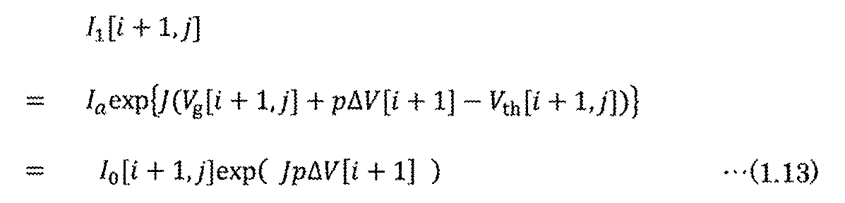

式(1.13)、式(1.14)より、x[i+1]は次の式で表すことができる。

そのため、式(1.13)は、次の式に書き換えることができる。

つまり、セルIM[i+1,j]に含まれているトランジスタF2の第1端子−第2端子間に流れる電流量は、第1データであるw[i+1,j]と、第2データであるx[i+1]と、の積に比例する。
ここで、変換回路ITRZ[j]から、トランジスタF4[j]と配線WCL[j]とを介して、セルIM[i,j]及びセルIM[i+1,j]に流れる電流量の総和を考える。当該電流量の総和をIS[j]とすると、IS[j]は、式(1.12)と式(1.16)より、次の式で表すことができる。

したがって、変換回路ITRZ[j]から出力される電流量は、第1データである重み係数w[i,j]及びw[i+1,j]と、第2データであるニューロンの信号の値x[i]及びx[i+1]と、の積和に比例した電流量となる。
なお、上述の動作例では、セルIM[i,j]、及びセルIM[i+1,j]に流れる電流量の総和について扱ったが、複数のセルとして、セルIM[1,j]乃至セルIM[m,j]のそれぞれに流れる電流量の総和についても扱ってもよい。この場合、式(1.17)は、次の式に書き直すことができる。

このため、3行以上且つ2列以上のセルアレイCAを有する演算回路MAC1の場合でも、上記の通り、積和演算を行うことができる。この場合の演算回路MAC1は、複数列のうち1列を、電流量としてIref0、及びxIref0を保持するセルとすることで、複数列のうち残りの列の数だけ積和演算処理を同時に実行することができる。つまり、メモリセルアレイの列の数を増やすことで、高速な積和演算処理を実現する半導体装置を提供することができる。
なお、上述した演算回路MAC1の動作例は、正の第1データと正の第2データとの積和を演算する場合に好適である。なお、正又は負の第1データと、正の第2データとの積和を演算する動作例、また、正又は負の第1データと、正又は負の第2データと、の積和を演算する動作例については、実施の形態2で説明する。
また、本実施の形態では、演算回路MAC1に含まれているトランジスタをOSトランジスタ、又はSiトランジスタとした場合について説明したが、本発明の一態様は、これに限定されない。演算回路MAC1に含まれているトランジスタは、例えば、Geなどがチャネル形成領域に含まれるトランジスタ、ZnSe、CdS、GaAs、InP、GaN、SiGeなどの化合物半導体がチャネル形成領域に含まれるトランジスタ、カーボンナノチューブがチャネル形成領域に含まれるトランジスタ、有機半導体がチャネル形成領域に含まれるトランジスタ等を用いることができる。
なお、本実施の形態は、本明細書で示す他の実施の形態と適宜組み合わせることができる。
(実施の形態2)
実施の形態1では、正又は“0”の第1データと正又は“0”の第2データとの積和を行う演算回路、及びその動作例について説明したが、本実施の形態では、正、負、又は“0”の第1データと、正、又は“0”の第2データと、の積和演算、及び、正、負、又は“0”の第1データと、正、負、又は“0”の第2データと、の積和演算が可能な演算回路について説明する。
実施の形態1では、正又は“0”の第1データと正又は“0”の第2データとの積和を行う演算回路、及びその動作例について説明したが、本実施の形態では、正、負、又は“0”の第1データと、正、又は“0”の第2データと、の積和演算、及び、正、負、又は“0”の第1データと、正、負、又は“0”の第2データと、の積和演算が可能な演算回路について説明する。
<演算回路の構成例1>
図7は、正、負、又は“0”の第1データと、正、又は“0”の第2データとの積和演算を行う演算回路の構成例を示している。図7に示す演算回路MAC2は、図1の演算回路MAC1を変更した構成となっている。そのため、演算回路MAC2の説明において、演算回路MAC1の説明と重複する部分については省略する。
図7は、正、負、又は“0”の第1データと、正、又は“0”の第2データとの積和演算を行う演算回路の構成例を示している。図7に示す演算回路MAC2は、図1の演算回路MAC1を変更した構成となっている。そのため、演算回路MAC2の説明において、演算回路MAC1の説明と重複する部分については省略する。
図7に示すセルアレイCAは、回路CES[1,j]乃至回路CES[m,j]を有し、回路CES[1,j]は、セルIM[1,j]と、セルIMr[1,j]と、を有し、回路CES[m,j]は、セルIM[m,j]と、セルIMr[m,j]と、を有する。なお、図7では、回路CES[1,j]と回路CES[m,j]とを抜粋して図示している。また、本明細書等では、回路CES[1,j]乃至回路CES[m,j]、セルIM[1,j]、セルIMr[1,j]、セルIM[m,j]、セルIMr[m,j]などを説明する際、それぞれの符号に付記している[m,n]などを省略する場合がある。
セルIMは、図1の演算回路MAC1のセルアレイCAに含まれているセルIM[1,1]乃至セルIM[m,n]と同様の構成とすることができる。
また、セルIMrは、セルIMと同様の構成とすることができる。図7のセルIMrは、一例として、セルIMと同様の構成として図示している。また、セルIMとセルIMrとのそれぞれに含まれているトランジスタ、容量などを互いに区別できるように、セルIMrに含まれているトランジスタ、容量を示す符号には「r」を付している。
具体的には、セルIMrは、トランジスタF1rと、トランジスタF2rと、容量C5rと、を有する。なお、トランジスタF1rはセルIMのトランジスタF1に相当し、トランジスタF2rはセルIMのトランジスタF2に相当し、容量C5rはセルIMの容量C5に相当する。そのため、トランジスタF1rと、トランジスタF2rと、容量C5rと、のそれぞれの電気的な接続構成については、実施の形態1のIM[1,1]乃至セルIM[m,n]の説明を参酌する。
また、セルIMrにおいて、トランジスタF1rの第1端子と、トランジスタF2rのゲートと、容量C5rの第1端子と、の接続箇所をノードNNrとしている。
回路CES[1,j]において、容量C5の第2端子は、配線XCL[1]に電気的に接続され、トランジスタF1のゲートは、配線WSL[1]に電気的に接続され、トランジスタF1の第2端子とトランジスタF2の第2端子とは、配線WCL[j]に電気的に接続されている。また、容量C5rの第2端子は、配線XCL[1]に電気的に接続され、トランジスタF1rのゲートは、配線WSL[1]に電気的に接続され、トランジスタF1rの第2端子とトランジスタF2rの第2端子とは、配線WCLr[j]に電気的に接続されている。
同様に、回路CES[m,j]において、容量C5の第2端子は、配線XCL[m]に電気的に接続され、トランジスタF1のゲートは、配線WSL[m]に電気的に接続され、トランジスタF1の第2端子とトランジスタF2の第2端子とは、配線WCL[j]に電気的に接続されている。また、容量C5rの第2端子は、配線XCL[m]に電気的に接続され、トランジスタF1rのゲートは、配線WSL[m]に電気的に接続され、トランジスタF1rの第2端子とトランジスタF2rの第2端子とは、配線WCLr[j]に電気的に接続されている。
配線WCL[j]及び配線WCLr[j]のそれぞれは、実施の形態1で説明した配線WCL[1]乃至配線WCL[n]と同様に、一例として、回路WCSから回路CESに含まれているセルIMとセルIMrに電流を流す配線として機能する。また、一例として、変換回路ITRZD[j]から回路CESに含まれているセルIMとセルIMrに電流を流す配線として機能する。
また、図7の演算回路MAC2において、回路SWS1は、トランジスタF3[j]と、トランジスタF3r[j]と、を有する。トランジスタF3[j]の第1端子は、配線WCL[j]に電気的に接続され、トランジスタF3[j]の第2端子は、回路WCSに電気的に接続され、トランジスタF3[j]のゲートは、配線SWL1に電気的に接続されている。また、トランジスタF3r[j]の第1端子は、配線WCLr[j]に電気的に接続され、トランジスタF3r[j]の第2端子は、回路WCSに電気的に接続され、トランジスタF3r[j]のゲートは、配線SWL1に電気的に接続されている。
また、図7の演算回路MAC2において、回路SWS2は、トランジスタF4[j]と、トランジスタF4r[j]と、を有する。トランジスタF4[j]の第1端子は、配線WCL[j]に電気的に接続され、トランジスタF4[j]の第2端子は、変換回路ITRZD[j]に電気的に接続され、トランジスタF4[j]のゲートは、配線SWL2に電気的に接続されている。また、トランジスタF4r[j]の第1端子は、配線WCLr[j]に電気的に接続され、トランジスタF4r[j]の第2端子は、変換回路ITRZD[j]に電気的に接続され、トランジスタF4r[j]のゲートは、配線SWL2に電気的に接続されている。
変換回路ITRZD[j]は、演算回路MAC1における変換回路ITRZ[j]乃至変換回路ITRZ[n]に相当する回路であって、例えば、変換回路ITRZD[j]から配線WCL[j]に流れる電流の量と、変換回路ITRZD[j]から配線WCLr[j]に流れる電流の量と、の差分に応じた電圧を生成して、配線OL[j]に出力する機能を有する。
変換回路ITRZD[j]の具体的な構成例を図8Aに示す。図8Aに示す変換回路ITRZD1は、図7の変換回路ITRZD[j]に適用できる回路の一例である。なお、図8Aには、変換回路ITRZD1の周辺の回路との電気的な接続を示すため、回路SWS2、配線WCL、配線WCLr、配線SWL2、トランジスタF4、トランジスタF4rも図示している。また、配線WCL及び配線WCLrのそれぞれは、一例として、図7の演算回路MAC2に含まれている配線WCL[j]及び配線WCLr[j]とし、トランジスタF4及びトランジスタF4rは、一例として、図7の演算回路MAC2に含まれているトランジスタF4[j]及びトランジスタF4r[j]とすることができる。
図8Aの変換回路ITRZD1は、トランジスタF4を介して配線WCLに電気的に接続されている。また、変換回路ITRZD1は、トランジスタF4rを介して配線WCLrに電気的に接続されている。また、変換回路ITRZD1は、配線OLに電気的に接続されている。変換回路ITRZD1は、変換回路ITRZD1から配線WCLに流れる電流量、又は配線WCLから変換回路ITRZD1に流れる電流量を第1の電圧に変換する機能と、変換回路ITRZD1から配線WCLrに流れる電流量、又は配線WCLrから変換回路ITRZD1に流れる電流量を第2の電圧に変換する機能と、第1の電圧と第2の電圧との差に応じたアナログ電圧を配線OLに出力する機能と、を有する。
図8Aの変換回路ITRZD1は、一例として、抵抗RPと、抵抗RMと、オペアンプOPPと、オペアンプOPMと、オペアンプOP2と、を有する。
オペアンプOPPの反転入力端子は、抵抗RPの第1端子と、トランジスタF4の第2端子と、に電気的に接続されている。オペアンプOPPの非反転入力端子は、配線VRPLに電気的に接続されている。オペアンプOPPの出力端子は、抵抗RPの第2端子と、オペアンプOP2の非反転入力端子に電気的に接続されている。また、オペアンプOPMの反転入力端子は、抵抗RMの第1端子と、トランジスタF4rの第2端子と、に電気的に接続されている。オペアンプOPMの非反転入力端子は、配線VRMLに電気的に接続されている。オペアンプOPMの出力端子は、抵抗RMの第2端子と、オペアンプOP2の反転入力端子に電気的に接続されている。オペアンプOP2の出力端子は、配線OLに電気的に接続されている。
配線VRPLは、定電圧を与える配線として機能する。当該定電圧としては、例えば、接地電位(GND)、低レベル電位などとすることができる。また、配線VRMLは、定電圧を与える配線として機能する。当該定電圧としては、例えば、接地電位(GND)、低レベル電位などとすることができる。また、配線VRPL及び配線VRMLのそれぞれが与える定電圧は、互いに等しくてもよいし、互いに異なっていてもよい。特に、配線VRPL及び配線VRMLのそれぞれが与える定電圧を接地電位(GND)にすることによって、オペアンプOPPの反転入力端子、及びオペアンプOPMの反転入力端子のそれぞれを仮想接地にすることができる。
変換回路ITRZD1は、図8Aの構成にすることによって、配線WCLから、トランジスタF4を介して、変換回路ITRZD1に流れる電流量、又は、変換回路ITRZD1から、トランジスタF4を介して、配線WCLに流れる電流量を、第1の電圧に変換することができる。また、配線WCLrから、トランジスタF4rを介して、変換回路ITRZD1に流れる電流量、又は、変換回路ITRZD1から、トランジスタF4rを介して、配線WCLrに流れる電流量を、第2の電圧に変換することができる。そして、第1の電圧と第2の電圧との差に応じたアナログ電圧を配線OLに出力することができる。
また、図8Aの変換回路ITRZD1は、アナログ電圧を出力する構成となっているが、図7の変換回路ITRZD[j]に適用できる回路構成は、これに限定されない。例えば、変換回路ITRZD1は、図4Bと同様に、図8Bに示すとおり、アナログデジタル変換回路ADCを有する構成としてもよい。具体的には、図8Bの変換回路ITRZD2は、アナログデジタル変換回路ADCの入力端子がオペアンプOP2の出力端子に電気的に接続され、アナログデジタル変換回路ADCの出力端子が配線OLに電気的に接続されている構成となっている。このような構成にすることによって、図8Bの変換回路ITRZD2は、配線OLにデジタル信号を出力することができる。
また、変換回路ITRZD2において、配線OLに出力されるデジタル信号を1ビット(2値)とする場合、変換回路ITRZ2は、図8Cに示す変換回路ITRZD3に置き換えてもよい。図8Cの変換回路ITRZ3は、図4Cと同様に、図8Aの変換回路ITRZD1にコンパレータCMP2を設けた構成となっている。具体的には、変換回路ITRZD3は、コンパレータCMP2の第1入力端子がオペアンプOP2の出力端子に電気的に接続され、コンパレータCMP2の第2入力端子が配線VRL3に電気的に接続され、コンパレータCMP2の出力端子が配線OLに電気的に接続されている構成となっている。配線VRL3は、コンパレータCMP2の第1端子の電位と比較するための電位を与える配線として機能する。このような構成にすることによって、図8Cの変換回路ITRZD3は、トランジスタF4のソース−ドレイン間に流れる電流量から変換された第1の電圧とトランジスタF4rのソース−ドレイン間に流れる電流量から変換された第2の電圧との差と、配線VRL3が与える電圧と、との大小に応じて、配線OLに低レベル電位又は高レベル電位(2値のデジタル信号)を出力することができる。
<<第1データの保持の例>>
次に、図7の演算回路MAC2において、正、負、又は“0”の第1データと、正、又は“0”の第2データとの積和演算を行うための、第1データを回路CESに保持する一例について説明する。
次に、図7の演算回路MAC2において、正、負、又は“0”の第1データと、正、又は“0”の第2データとの積和演算を行うための、第1データを回路CESに保持する一例について説明する。
回路CESは、セルIMと、セルIMrと、を有するため、回路CESは、第1データの保持として、セルIMと、セルIMrと、の2つの回路を用いることができる。つまり、回路CESは、2つの電流量を設定して、それぞれの電流量に応じた電位をセルIMと、セルIMrと、に保持することができる。このため、第1データを、セルIMで設定される電流量と、セルIMrで設定される電流量と、で表すことができる。ここで、回路CESに保持される、正の第1データ、負の第1データ、又は“0”の第1データを次の通りに定義する。
回路CES[1,j]に正の第1データを保持する場合、セルIM[1,j]には、一例として、セルIM[1,j]のトランジスタF2の第1端子−第2端子間に正の第1データの値の絶対値に応じた電流量が流れるように設定する。具体的には、トランジスタF2のゲート(ノードNN[1,j])に当該電流量に応じた電位を保持する。一方、セルIMr[1,j]には、一例として、セルIMr[1,j]のトランジスタF2rの第1端子−第2端子間に電流が流れないように設定する。具体的には、トランジスタF2rのゲート(ノードNNr[1,j])には、配線VEが与える電位、図2Aの回路WCSの配線VINIL1が与える初期化用の電位などが保持されていればよい。
また、回路CES[1,j]に負の第1データを保持する場合、セルIMr[1,j]には、一例として、セルIMr[1,j]のトランジスタF2rには負の第1データの値の絶対値に応じた電流量が流れるように設定する。具体的には、トランジスタF2rのゲート(ノードNNr[1,j])に当該電流量に応じた電位を保持する。一方、セルIM[1,j]は、一例として、セルIM[1,j]のトランジスタF2には電流が流れないように設定する。具体的には、トランジスタF2のゲート(ノードNN[1,j])には、配線VEが与える電位、図2Aの回路WCSの配線VINIL1が与える初期化用の電位などが保持されていればよい。
また、回路CES[1,j]に“0”の第1データを保持する場合、一例として、セルIM[1,j]のトランジスタF2、及びセルIMr[1,j]のトランジスタF2rのそれぞれには電流が流れないように設定する。具体的には、トランジスタF2のゲート(ノードNN[1,j])とトランジスタF2rのゲート(ノードNNr[1,j])には、配線VEが与える電位、図2Aの回路WCSの配線VINIL1が与える初期化用の電位などが保持されていればよい。
なお、他の回路CESについても、正の第1データ、又は負の第1データを保持するとき、上述した回路CES[1,j]と同様に、セルIMと配線WCLとの間、セルIMrと配線WCLrとの間、の一方には第1データに応じた電流量が流れるように設定し、セルIMと配線WCLとの間、セルIMrと配線WCLrとの間、の他方には電流が流れないように設定すればよい。また、他の回路CESに、“0”の第1データを保持するとき、上述した回路CES[1,j]と同様に、セルIMと配線WCLとの間、及びセルIMrと配線WCLrとの間には電流が流れないように設定すればよい。
一例として、“+3”、“+2”、“+1”、“0”、“−1”、“−2”、“−3”のそれぞれの場合を第1データとして回路CESに保持するとき、配線WCLからセルIMに流れる電流量の設定、及び配線WCLrからセルIMrに流れる電流量の設定を上記のとおりに従うことで、第1データ“+3”、“+2”、“+1”、“0”、“−1”、“−2”、“−3”のそれぞれは、例えば、次表のとおりに定義することができる。
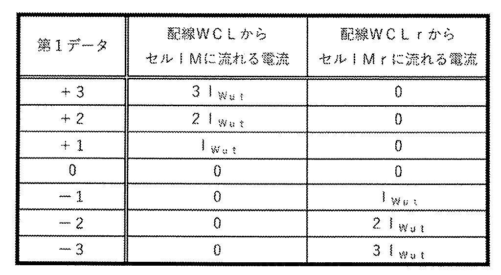
ここで、図7の演算回路MAC2において、回路CES[1,j]乃至回路CES[m,j]のそれぞれに第1データが保持され、配線XCL[1]乃至配線XCL[m]のそれぞれに第2データが入力された場合を考える。このとき、配線SWL1に低レベル電位を与えてトランジスタF3[j]、及びトランジスタF3r[j]をオフ状態にし、このとき、配線SWL2に高レベル電位を与えてトランジスタF4[j]、及びトランジスタF4r[j]をオン状態にする。これにより、変換回路ITRZD[j]と配線WCL[j]との間が導通状態となるので、変換回路ITRZD[j]から配線WCL[j]に電流が流れる場合がある。また、変換回路ITRZD[j]と配線WCLr[j]との間が導通状態となるので、変換回路ITRZD[j]から配線WCLr[j]に電流が流れる場合がある。変換回路ITRZD[j]から配線WCL[j]に流れる電流量の総和をIS[j]とし、及び変換回路ITRZD[j]から配線WCLr[j]に流れる電流量の総和をISr[j]として、実施の形態1で説明した演算回路MAC1の動作例を参酌すると、IS[j]及びISr[j]は、次の式で表すことができる。
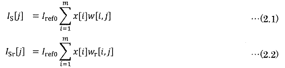
なお、式(2.1)に示すw[i,j]は、セルIM[i,j]に書き込まれる第1データの値であり、式(2.2)に示すwr[i,j]は、セルIMr[i,j]に書き込まれる第1データの値である。なお、w[i,j]、又はwr[i,j]の一方が“0”でない値であるとき、w[i,j]、又はwr[i,j]の他方は“0”の値とすることによって、回路CES[i,j]に保持される第1データは、例えば、表1に示した定義などに従うことができる。
変換回路ITRZD[j]は、例えば、配線WCLに流れる電流量の総和IS[j]を第1の電圧に変換し、配線WCLrに流れる電流量の総和ISr[j]を第2の電圧に変換する。そして、変換回路ITRZD[j]は、第1の電圧と第2の電圧との差に応じた電圧を配線OLに出力することができる。
ところで、図8A乃至図8Cのそれぞれに示した変換回路ITRZD1乃至変換回路ITRZD3は、配線OLに電圧を出力する回路構成としたが、本発明の一態様は、これに限定されない。例えば、図7の演算回路MAC2に含まれている変換回路ITRZD[j]は、電流を出力する回路構成としてもよい。
図9に示す変換回路ITRZD4は、図7の演算回路MAC2に含まれている変換回路ITRZD[j]に適用することができる回路であり、積和演算及び活性化関数の演算の結果を電流量として出力する回路構成となっている。
なお、図9には、変換回路ITRZD4の周辺の回路との電気的な接続を示すため、回路SWS2、配線WCL、配線WCLr、配線OL、トランジスタF4、トランジスタF4rも図示している。また、配線WCL及び配線WCLrのそれぞれは、一例として、図7の演算回路MAC2に含まれている配線WCL[j]及び配線WCLr[j]とし、トランジスタF4及びトランジスタF4rは、一例として、図7の演算回路MAC2に含まれているトランジスタF4[j]及びトランジスタF4r[j]とすることができる。
図9の変換回路ITRZD4は、トランジスタF4を介して配線WCLに電気的に接続されている。また、変換回路ITRZD4は、トランジスタF4rを介して配線WCLrに電気的に接続されている。また、変換回路ITRZD4は、配線OLに電気的に接続されている。変換回路ITRZD4は、変換回路ITRZD4から配線WCLに流れる電流量、又は配線WCLから変換回路ITRZD4に流れる電流量の一方と、変換回路ITRZD4から配線WCLrに流れる電流量、又は配線WCLrから変換回路ITRZD4に流れる電流量の一方と、の差分電流を取得する機能を有する。また、当該差分電流を、変換回路ITRZD4と配線OLとの間に流す機能を有する。
図9の変換回路ITRZD4は、一例として、トランジスタF5と、電流源CIと、電流源CIrと、カレントミラー回路CM1と、を有する。
トランジスタF4の第2端子は、カレントミラー回路CM1の第1端子と、電流源CIの出力端子と、に電気的に接続され、トランジスタF4rの第2端子は、カレントミラー回路CM1の第2端子と、電流源CIrの出力端子と、トランジスタF5の第1端子と、に電気的に接続されている。また、電流源CIの入力端子は、配線VHEに電気的に接続され、電流源CIrの入力端子は、配線VHEに電気的に接続されている。また、カレントミラー回路CM1の第3端子は、配線VSEに電気的に接続され、カレントミラー回路CM1の第4端子は、配線VSEに電気的に接続されている。
トランジスタF5の第2端子は、配線OLに電気的に接続され、トランジスタF5のゲートは、配線OELに電気的に接続されている。
カレントミラー回路CM1は、一例として、カレントミラー回路CM1の第1端子の電位に応じた電流量を、カレントミラー回路CM1の第1端子と第3端子との間と、カレントミラー回路CM1の第2端子と第4端子との間と、に流す機能を有する。
配線VHEは、例えば、定電圧を与える配線として機能する。具体的には、例えば、当該定電圧としては、高レベル電位などとすることができる。
配線VSEは、例えば、定電圧を与える配線として機能する。具体的には、例えば、当該定電圧としては、低レベル電位、接地電位などとすることができる。
配線OELは、例えば、トランジスタF5のオン状態、又はオフ状態に切り替えるための信号を送信するための配線として機能する。具体的には、例えば、配線OELには、高レベル電位、又は低レベル電位を入力すればよい。
電流源CIは、電流源CIの入力端子と出力端子との間に定電流を流す機能を有する。また、電流源CIrは、電流源CIrの入力端子と出力端子との間に定電流を流す機能を有する。なお、図9の変換回路ITRZD4において、電流源CIが流す電流の大きさと、電流源CIrが流す電流の大きさと、は等しいことが好ましい。
ここで、図9の変換回路ITRZD4の動作例について、説明する。
初めに、変換回路ITRZD4からトランジスタF4を介して配線WCLに流れる電流の量をISとし、変換回路ITRZD4からトランジスタF4rを介して配線WCLrに流れる電流の量をISrとする。また、電流源CI及び電流源CIrのそれぞれが流す電流の量をI0とする。
ISは、図7の演算回路MAC2において、例えば、j列目に位置するセルIM[1,j]乃至セルIM[m,j]に流れる電流量の総和とする。また、ISrは、図7の演算回路MAC2において、例えば、j列目に位置するセルIMr[1,j]乃至セルIMr[m,j]に流れる電流量の総和とする。
配線SWL2に高レベル電位が入力されることによって、トランジスタF4、及びトランジスタF4rはオン状態となる。このため、カレントミラー回路CM1の第1端子から第3端子に流れる電流量は、I0−ISとなる。また、カレントミラー回路CM1によって、カレントミラー回路CM1の第2端子から第2端子にI0−ISの電流量が流れる。
次に、配線OELに高レベル電位が入力されて、トランジスタF5がオン状態となる。このとき、配線OLに流れる電流量をIoutとすると、Iout=I0−(I0−IS)−ISr=IS−ISrとなる。
ここで、図7の演算回路MAC2において、正、負、又は“0”の第1データと、正、又は“0”の第2データとの積和演算を行うための、第1データの回路CESへの保持については、上記の第1データの保持の例を参酌する。
つまり、回路CES[i,j]に正の第1データを保持する場合、セルIM[i,j]には、セルIM[i,j]のトランジスタF2の第1端子−第2端子間に正の第1データの値の絶対値に応じた電流量が流れるように設定し、セルIMr[i,j]には、セルIMr[i,j]のトランジスタF2rの第1端子−第2端子間に電流が流れないように設定する。また、回路CES[i,j]に負の第1データを保持する場合、セルIM[i,j]には、セルIM[i,j]のトランジスタF2の第1端子−第2端子間に電流が流れないように設定し、セルIMr[i,j]には、セルIMr[i,j]のトランジスタF2rの第1端子−第2端子間に負の第1データの値の絶対値に応じた電流量が流れるように設定する。また、回路CES[i,j]に“0”の第1データを保持する場合、セルIM[i,j]には、セルIM[i,j]のトランジスタF2の第1端子−第2端子間に電流が流れないように設定し、セルIMr[i,j]には、セルIMr[i,j]のトランジスタF2rの第1端子−第2端子間に電流が流れないように設定する。
ここで、図7の演算回路MAC2の配線XCL[1]乃至配線XCL[m]のそれぞれに第2データが入力された場合、セルIM[i,j]のトランジスタF2の第1端子−第2端子間に流れる電流量、及びセルIMr[i,j]のトランジスタF2の第1端子−第2端子間に流れる電流量のそれぞれは、第2データに比例する。
ISはj列目に位置するセルIM[1,j]乃至セルIM[m,j]に流れる電流量の総和である。そのため、ISは、回路CES[1,j]乃至回路CES[m,j]のうち、正の第1データが保持された回路CESに含まれている、セルIMに流れる電流量の総和となり、例えば、式(2.1)と同様に表すことができる。つまり、ISは、正の第1データの絶対値と第2データとの積和演算の結果に対応する。また、ISrはj列目に位置するセルIMr[1,j]乃至セルIMr[m,j]に流れる電流量の総和である。そのため、ISrは、回路CES[1,j]乃至回路CES[m,j]のうち、負の第1データが保持された回路CESに含まれている、セルIMrに流れる電流量の総和となり、例えば、式(2.2)と同様に表すことができる。つまり、ISrは、負の第1データの絶対値と第2データとの積和演算の結果に対応する。
このため、配線OLに流れる電流量Iout=IS−ISrは、正の第1データの絶対値と第2データとの積和演算の結果と、負の第1データの絶対値と第2データとの積和演算の結果と、の差に対応する。つまり、Iout=IS−ISrは、回路CES[1,j]乃至回路CES[m,j]に保持されている、負、“0”、又は正の第1データと、配線XCL[1]乃至配線XCL[m]のそれぞれに入力される第2データとの積和演算の結果に対応する。
ところで、セルIM[1,j]乃至セルIM[m,j]に流れる電流量の総和が、セルIMr[1,j]乃至セルIMr[m,j]に流れる電流量の総和よりも大きいとき、すなわちISがISrよりも大きいとき、Ioutは0よりも大きい電流量となり、変換回路ITRZD4から配線OLに流れる。一方、セルIM[1,j]乃至セルIM[m,j]に流れる電流量の総和が、セルIMr[1,j]乃至セルIMr[m,j]に流れる電流量の総和よりも小さいとき、すなわちISがISrよりも小さいとき、配線OLから変換回路ITRZD4に電流が流れない場合がある。つまり、ISがISrよりも小さいとき、Ioutは概ね0とすることができる。このため、変換回路ITRZD4は、例えば、ReLU関数として作用するとみなすことができる。
ReLU関数は、例えば、ニューラルネットワークの活性化関数に利用することができる。ニューラルネットワークの演算では、前層のニューロンのそれぞれの信号の値(例えば、第2データとすることができる)と、対応する重み係数(例えば、第1データとすることができる)と、の積和を算出する必要がある。また、積和の結果に応じて活性化関数の値を計算する必要がある。このため、ニューラルネットワークの活性化関数をReLU関数とした場合、当該ニューラルネットワークの演算は、変換回路ITRZD4を含む演算回路MAC2を用いることによって行うことができる。
なお、階層型のニューラルネットワークについては、実施の形態5で後述する。
次に、図9の変換回路ITRZD4の具体的な回路構成の例について説明する。
図10Aに示す変換回路ITRZD4は、図9の変換回路ITRZD4の一例である。具体的には、図10Aでは、カレントミラー回路CM1、電流源CI、及び電流源CIrのそれぞれの構成の例を示している。
図10Aの変換回路ITRZD4において、カレントミラー回路CM1は、一例として、トランジスタF6と、トランジスタF6rと、を有し、電流源CIは、一例として、トランジスタF7を有し、電流源CIrは、一例として、トランジスタF7rを有する。なお、トランジスタF6、トランジスタF6r、トランジスタF7、及びトランジスタF7rは、nチャネル型トランジスタとしている。
例えば、カレントミラー回路CM1の第1端子は、トランジスタF6の第1端子と、トランジスタF6のゲートと、トランジスタF6rのゲートと、に電気的に接続され、カレントミラー回路CM1の第3端子は、トランジスタF6の第2端子に電気的に接続されている。また、カレントミラー回路CM1の第2端子は、トランジスタF6rの第1端子に電気的に接続され、カレントミラー回路CM1の第4端子は、トランジスタF6rの第2端子に電気的に接続されている。
また、例えば、電流源CIの出力端子は、トランジスタF7の第1端子と、トランジスタF7のゲートと、に電気的に接続され、電流源CIの入力端子は、トランジスタF7の第2端子に電気的に接続されている。
また、例えば、電流源CIrの出力端子は、トランジスタF7rの第1端子と、トランジスタF7rのゲートと、に電気的に接続され、電流源CIrの入力端子は、トランジスタF7rの第2端子に電気的に接続されている。
トランジスタF7、及びトランジスタF7rのそれぞれは、ゲートと第1端子とが電気的に接続されており、かつ第2端子と配線VHEとが電気的に接続されている。したがって、トランジスタF7、及びトランジスタF7rのそれぞれのゲート−ソース間電圧は0Vとなり、トランジスタF7、及びトランジスタF7rのそれぞれのしきい値電圧が適切な範囲内である場合、トランジスタF7、及びトランジスタF7rのそれぞれの第1端子−第2端子間には定電流が流れる。つまり、トランジスタF7、及びトランジスタF7rのそれぞれは電流源として機能する。
なお、図9の変換回路ITRZD4に含まれる電流源CI、及び電流源CIrの構成は、図10Aに示した電流源CI、及び電流源CIrに限定されない。変換回路ITRZD4に含まれる電流源CI、及び電流源CIrのそれぞれの構成は、状況に応じて、変更を行ってもよい。
例えば、図9の変換回路ITRZD4に含まれる電流源CI、及び電流源CIrのそれぞれは、図10Bに示す電流源CI(電流源CIr)としてもよい。
図10Bの電流源CI(電流源CIr)は、一例として、複数の電流源CSAを有する。また、複数の電流源CSAのそれぞれは、トランジスタF7と、トランジスタF7sと、端子U1と、端子U2と、端子U3と、を有する。
電流源CSAは、一例として、端子U2と端子U1との間に電流量としてICSAを流す機能を有する。また、電流源CI(電流源CIr)は、例えば、2P−1個(Pは1以上の整数である)の電流源CSAを有するものとしたとき、電流源CI(電流源CIr)は、出力端子に電流量としてs×ICSA(sは0以上2P−1以下の整数である)を流すことができる。
なお、実際には、電流源CI(電流源CIr)の作製段階において、それぞれの電流源CSAに含まれているトランジスタの電気特性のバラツキによって誤差が現れることがある。そのため、複数の電流源CSAの端子U1のそれぞれから出力される定電流ICSAの誤差は10%以内が好ましく、5%以内であることがより好ましく、1%以内であることがより好ましい。なお、本実施の形態では、電流源CI(電流源CIr)に含まれている複数の電流源CSAの端子U1から出力される定電流ICSAの誤差は無いものとして説明する。
複数の電流源CSAの一において、トランジスタF7sの第1端子は、端子U1に電気的に接続され、トランジスタF7sのゲートは、端子U3に電気的に接続されている。トランジスタF7の第1端子は、トランジスタF7のゲートと、トランジスタF7sの第2端子と、に電気的に接続されている。トランジスタF7の第2端子は、端子U2に電気的に接続されている。
複数の電流源CSAのそれぞれの端子U1は、電流源CI(電流源CIr)の出力端子に電気的に接続されている。また、複数の電流源CSAのそれぞれの端子U2は、電流源CI(電流源CIr)の入力端子に電気的に接続されている。つまり、複数の電流源CSAのそれぞれの端子U2と、配線VHEと、の間は導通となっている。
また、1個の電流源CSAの端子U3は配線CL[1]に電気的に接続され、2個の電流源CSAの端子U3のそれぞれは配線CL[2]に電気的に接続され、2P−1個の電流源CSの端子U3のそれぞれは配線CL[P]に電気的に接続されている。
配線CL[1]乃至配線CL[P]は、電気的に接続されている電流源CSAから定電流ICSAを出力するための制御信号を送信する配線として機能する。具体的には、例えば、配線CL[1]に高レベル電位が与えられているとき、配線CL[1]に電気的に接続されている電流源CSAは、定電流としてICSAを端子U1に流し、また、配線CL[1]に低レベル電位が与えられているとき、配線CL[1]に電気的に接続されている電流源CSAは、ICSAを出力しない。また、例えば、配線CL[2]に高レベル電位が与えられているとき、配線CL[2]に電気的に接続されている2個の電流源CSAは、合計2ICSAを定電流として端子U1に流し、また、配線CL[2]に低レベル電位が与えられているとき、配線CL[2]に電気的に接続されている電流源CSAは、合計2ICSAの定電流を出力しない。また、例えば、配線CL[P]に高レベル電位が与えられているとき、配線CL[P]に電気的に接続されている2P−1個の電流源CSAは、合計2P−1ICSAを定電流として端子U1に流し、また、配線CL[P]に低レベル電位が与えられているとき、配線CL[P]に電気的に接続されている電流源CSAは、合計2P−1ICSAの定電流を出力しない。
このため、電流源CI(電流源CIr)は、配線CL[1]乃至配線CL[P]から選ばれた一本以上の配線に高レベル電位を与えることによって、電流源CI(電流源CIr)の出力端子に電流を流すことができる。また、当該電流の量は、高レベル電位を入力する、配線CL[1]乃至配線CL[P]から選ばれた一本以上の配線の組み合わせによって定めることができる。例えば、配線CL[1]及び配線CL[2]に高レベル電位か与えられ、配線CL[3]乃至配線CL[P]に低レベル電位が与えられているとき、電流源CI(電流源CIr)は、電流源CI(電流源CIr)の出力端子に合計3ICSAの電流を流すことができる。
上記の通り、図10Bの電流源CI(電流源CIr)を用いることによって、状況に応じて、電流源CI(電流源CIr)が出力端子に流す電流量を変化させることができる。
また、図9の変換回路ITRZD4として、図10Aの変換回路ITRZD4を適用することによって、変換回路ITRZD4に含まれるすべてのトランジスタをOSトランジスタとすることができる。また、演算回路MAC2のセルアレイCA、回路WCS、回路XCSなどは、OSトランジスタのみで構成することができるため、変換回路ITRZD4は、セルアレイCA、回路WCS、回路XCSなどと同時に作製することができる。そのため、演算回路MAC2の作製工程を短縮することができる場合がある。なお、これは、図10Aの変換回路ITRZD4の電流源CI及び電流源CIrに図10Bの電流源CI(電流源CIr)を適用した場合についても同様である。
例えば、図9の変換回路ITRZD4に含まれる電流源CI、及び電流源CIrのそれぞれは、互いに同じ電流を流す必要があるため、電流源CI、及び電流源CIrのそれぞれをカレントミラー回路に置き換えてもよい。
図11Aに示す変換回路ITRZD4は、図9の変換回路ITRZD4に含まれる電流源CI、及び電流源CIrのそれぞれをカレントミラー回路CM2に置き換えた構成となっている。カレントミラー回路CM2は、一例として、トランジスタF8と、トランジスタF8rと、を有する。なお、トランジスタF8、及びトランジスタF8rは、pチャネル型トランジスタとしている。
トランジスタF8の第1端子は、トランジスタF8のゲートと、トランジスタF8rのゲートと、トランジスタF4の第2端子と、カレントミラー回路CM1の第1端子と、に電気的に接続されている。トランジスタF8の第2端子は、配線VHEに電気的に接続されている。トランジスタF8rの第1端子は、トランジスタF4rの第2端子と、カレントミラー回路CM1の第2端子と、に電気的に接続されている。トランジスタF8rの第2端子は、配線VHEに電気的に接続されている。
図11Aの変換回路ITRZD4のとおり、図9の変換回路ITRZD4に含まれる電流源CI、及び電流源CIrのそれぞれをカレントミラー回路CM2に置き換えることによって、トランジスタF4の第2端子とカレントミラー回路CM1の第1端子との接続点、及びトランジスタF4rの第2端子とカレントミラー回路CM1の第2端子とトランジスタF5の第1端子との接続点のそれぞれに互いにほぼ等しい電流量を流すことができる。
なお、図11Aでは、カレントミラー回路CM2をトランジスタF8と、トランジスタF8rと、からなる構成として図示したが、カレントミラー回路CM2の回路構成は、これに限定されない。例えば、カレントミラー回路CM2は、後述する図11Cと同様に、カレントミラー回路CM2に含まれるトランジスタをカスコード接続した構成としてもよい。このように、図11Aのカレントミラー回路CM2の回路構成は、状況に応じて変更を行ってもよい。
なお、図11Aの変換回路ITRZD4は、図11Bに示す変換回路ITRZD4に構成のとおり、カレントミラー回路CM1を設けない構成としてもよい。図11Bに示す変換回路ITRZD4は、カレントミラー回路CM2の第1端子からトランジスタF4の第2端子に流れる電流量と、カレントミラー回路CM2の第2端子からトランジスタF4rの第2端子と配線VSEとトランジスタF5の第1端子との接続点に流れる電流量と、を互いにほぼ等しくすることができる。そのため、ISがISrよりも大きい場合に、図11Bの配線OLに流れる電流量Ioutは、図9の変換回路ITRZD4と同様にIS−ISrとすることができる。
図11Bの変換回路ITRZD4は、カレントミラー回路CM1を設けない構成となっているため、図11Aの変換回路ITRZD4よりも回路面積を低減することができる。また、カレントミラー回路CM2からカレントミラー回路CM1に流れる定常電流が無くなるため、図11Bの変換回路ITRZD4は、図11Aの変換回路ITRZD4よりも消費電力を低減することができる。
なお、図11Bでは、トランジスタF8、及びトランジスタF8rを図示せず、カレントミラー回路CM2をブロック図として図示している。そのため、図11Bのカレントミラー回路CM2は、図11Aのカレントミラー回路CM2と同様に、状況に応じて、構成を決めることができる。
また、図9の変換回路ITRZD4に含まれるカレントミラー回路CM1は、図10Aに示したカレントミラー回路CM1に限定されない。図10Aの変換回路ITRZD4に含まれるカレントミラー回路CM1の構成は、状況に応じて、変更を行ってもよい。
例えば、図9の変換回路ITRZD4に含まれるカレントミラー回路CM1は、図11Cに示すカレントミラー回路CM1としてもよい。図11Cに示すカレントミラー回路CM1は、図10Aに示すカレントミラー回路CM1に更にnチャネル型トランジスタであるトランジスタF6s及びトランジスタF6srを設けて、トランジスタF6とトランジスタF6sとでカスコード接続し、トランジスタF6rとトランジスタF6srとでカスコード接続した構成となっている。図11Cのとおり、カレントミラー回路に含まれるトランジスタをカスコード接続することによって、当該カレントミラー回路の動作をより安定させることができる。
<演算回路の構成例2>
図12は、正、負、又は“0”の第1データと、正、負、又は“0”の第2データと、の積和演算を行う演算回路の構成例を示している。図12に示す演算回路MAC3は、図7の演算回路MAC2を変更した構成となっている。そのため、演算回路MAC3の説明において、演算回路MAC1及び演算回路MAC2の説明と重複する部分については省略する。
図12は、正、負、又は“0”の第1データと、正、負、又は“0”の第2データと、の積和演算を行う演算回路の構成例を示している。図12に示す演算回路MAC3は、図7の演算回路MAC2を変更した構成となっている。そのため、演算回路MAC3の説明において、演算回路MAC1及び演算回路MAC2の説明と重複する部分については省略する。
図12に示す回路CES[i,j]は、セルIM[i,j]と、セルIMr[i,j]と、に加え、セルIMs[i,j]と、セルIMsr[i,j]と、を有する。なお、図12では、回路CES[i,j]を図示しており、それ以外の回路CESについては省略する。また、本明細書等では、回路CES[i,j]、セルIM[i,j]、セルIMr[i,j]、セルIMs[i,j]、セルIMsr[i,j]などを説明する際、それぞれの符号に付記している[i,j]などを省略する場合がある。
セルIMs及びセルIMsrは、セルIMと同様の構成とすることができる。図12のセルIMs及びセルIMsrは、一例として、セルIMと同様の構成として図示している。また、セルIMとセルIMsとセルIMsrとのそれぞれに含まれているトランジスタ、容量などを互いに区別できるように、セルIMsに含まれているトランジスタ、容量を示す符号には「s」を付し、セルIMsrに含まれているトランジスタ、容量を示す符号には「sr」を付している。
具体的には、セルIMsは、トランジスタF1sと、トランジスタF2sと、容量C5sと、を有する。なお、トランジスタF1sはセルIMのトランジスタF1に相当し、トランジスタF2sはセルIMのトランジスタF2に相当し、容量C5sはセルIMの容量C5に相当する。そのため、トランジスタF1sと、トランジスタF2sと、容量C5sと、のそれぞれの電気的な接続構成については、実施の形態1のIM[1,1]乃至セルIM[m,n]の説明を参酌する。
また、セルIMsrは、トランジスタF1srと、トランジスタF2srと、容量C5srと、を有する。なお、トランジスタF1srはセルIMのトランジスタF1に相当し、トランジスタF2srはセルIMのトランジスタF2に相当し、容量C5srはセルIMの容量C5に相当する。そのため、トランジスタF1srと、トランジスタF2srと、容量C5srと、のそれぞれの電気的な接続構成については、セルIMsと同様に、実施の形態1のIM[1,1]乃至セルIM[m,n]の説明を参酌する。
また、セルIMsにおいて、トランジスタF1sの第1端子と、トランジスタF2sのゲートと、容量C5sの第1端子と、の接続箇所をノードNNsとし、セルIMsにおいて、トランジスタF1srの第1端子と、トランジスタF2srのゲートと、容量C5srの第1端子と、の接続箇所をノードNNsrとしている。
回路CES[i,j]において、容量C5の第2端子は、配線XCL[i]に電気的に接続され、トランジスタF1のゲートは、配線WSL[i]に電気的に接続され、トランジスタF1の第2端子とトランジスタF2の第2端子とは、配線WCL[j]に電気的に接続されている。また、容量C5rの第2端子は、配線XCL[i]に電気的に接続され、トランジスタF1rのゲートは、配線WSL[i]に電気的に接続され、トランジスタF1rの第2端子とトランジスタF2rの第2端子とは、配線WCLr[j]に電気的に接続されている。
また、容量C5sの第2端子は、配線XCLs[i]に電気的に接続され、トランジスタF1sのゲートは、配線WSLs[i]に電気的に接続され、トランジスタF1sの第2端子とトランジスタF2sの第2端子とは、配線WCL[j]に電気的に接続されている。また、容量C5srの第2端子は、配線XCLs[m]に電気的に接続され、トランジスタF1srのゲートは、配線WSLs[m]に電気的に接続され、トランジスタF1srの第2端子とトランジスタF2srの第2端子とは、配線WCLr[j]に電気的に接続されている。
図12に示す回路CESref[i]は、セルIMref[i]に加え、セルIMrefs[i]を有する。なお、図12では、回路CESref[i]を図示しており、それ以外の回路CESrefについては省略する。また、本明細書等では、回路CESref[i]、セルIMref[i]、セルIMrefs[i]などを説明する際、それぞれの符号に付記している[i]などを省略する場合がある。
セルIMrefsは、セルIMrefと同様の構成とすることができる。図12のセルIMrefsは、一例として、セルIMrefと同様の構成として図示している。また、セルIMrefとセルIMrefsとのそれぞれに含まれているトランジスタ、容量などを互いに区別できるように、セルIMrefsに含まれているトランジスタ、容量を示す符号には「s」を付している。
具体的には、セルIMrefsは、トランジスタF1msと、トランジスタF2msと、容量C5msと、を有する。なお、トランジスタF1msはセルIMrefのトランジスタF1mに相当し、トランジスタF2msはセルIMrefのトランジスタF2mに相当し、容量C5msはセルIMrefの容量C5mに相当する。そのため、トランジスタF1msと、トランジスタF2msと、容量C5msと、のそれぞれの電気的な接続構成については、実施の形態1のIMref[1]乃至セルIMref[m]の説明を参酌する。
また、セルIMrefsにおいて、トランジスタF1msの第1端子と、トランジスタF2msのゲートと、容量C5msの第1端子と、の接続箇所をノードNNrefsとしている。
回路CESref[i]において、容量C5mの第2端子は、配線XCL[i]に電気的に接続され、トランジスタF1mのゲートは、配線WSL[i]に電気的に接続され、トランジスタF1mの第2端子とトランジスタF2mの第2端子とは、配線XCL[i]に電気的に接続されている。また、容量C5msの第2端子は、配線XCLs[i]に電気的に接続され、トランジスタF1msのゲートは、配線WSLs[i]に電気的に接続され、トランジスタF1msの第2端子とトランジスタF2msの第2端子とは、配線XCLs[i]に電気的に接続されている。
配線XCL[i]及び配線XCLs[i]のそれぞれは、実施の形態1で説明した配線XCL[1]乃至配線XCL[n]と同様に、一例として、回路XCSから回路CESに含まれているセルIMとセルIMrとセルIMsとセルIMsrとに電流を流す配線、また、一例として、回路XCSから回路CESrefに含まれているセルIMref[i]とセルIMrefs[i]とに電流を流す配線として機能する。
配線WSL[j]及び配線WSLs[j]のそれぞれは、実施の形態1で説明した配線WSL[1]乃至配線WSL[m]と同様に、一例として、回路WSDから回路CESに含まれているセルIM及びセルIMrに対して、第1データを書き込むための選択信号を送信する配線、また、一例として、回路WSDから回路CESrefに含まれているセルIMref及びセルIMrefsに対して、参照データを書き込むための選択信号を送信する配線として機能する。
図12の演算回路MAC3に含まれる変換回路ITRZD[j]としては、図7の演算回路MAC2に含まれる変換回路ITRZD[j]に適用できる回路を用いることができる。つまり、演算回路MAC3に含まれる変換回路ITRZD[j]としては、例えば、図8A乃至図8Cに示す変換回路ITRZD1乃至変換回路ITRZD3を適用することができる。
次に、図12の演算回路MAC3において、正、負、又は“0”の第1データと、正、負、又は“0”の第2データとの積和演算を行うための、第1データを回路CESに保持する一例、及び第2データを回路CESに入力する一例について説明する。
回路CESは、セルIMと、セルIMrと、セルIMsと、セルIMsrと、を有するため、回路CESは、第1データの保持として、セルIMと、セルIMrと、セルIMsと、セルIMsrと、の4つの回路を用いることができる。つまり、回路CESは、4つの電流量を設定して、それぞれの電流量に応じた電位をセルIMと、セルIMrと、セルIMsと、セルIMsrと、に保持することができる。このため、第1データを、セルIMで設定される電流量と、セルIMrで設定される電流量と、セルIMsで設定される電流量と、セルIMsrで設定される電流量と、で表すことができる。ここで、回路CESに保持される、正の第1データ、負の第1データ、又は“0”の第1データを次の通りに定義する。
回路CES[i,j]に正の第1データを保持する場合、セルIM[i,j]には、一例として、セルIM[i,j]のトランジスタF2には正の第1データの値の絶対値に応じた電流量が流れるように設定し、また、セルIMsr[i,j]のトランジスタF2srには、一例として、正の第1データの値の絶対値に応じた電流量が流れるように設定する。具体的には、トランジスタF2のゲート(ノードNN[i,j])及びトランジスタF2srのゲート(ノードNNsr[i,j])に当該電流量に応じた電位を保持する。また、セルIMr[i,j]には、一例として、セルIMr[i,j]のトランジスタF2rには電流が流れないように設定し、また、セルIMs[i,j]には、一例として、セルIMs[i,j]のトランジスタF2sには電流が流れないように設定する。具体的には、トランジスタF2rのゲート(ノードNNr[i,j])及びトランジスタF2sのゲート(ノードNNs[i,j])には、配線VEが与える電位、図2の回路WCSの配線VINIL1が与える初期化用の電位などが保持されればよい。
また、回路CES[i,j]に負の第1データを保持する場合、セルIMr[i,j]には、一例として、セルIMr[1,j]のトランジスタF2rには負の第1データの値の絶対値に応じた電流量が流れるように設定し、また、セルIMs[i,j]のトランジスタF2sには、一例として、負の第1データの値の絶対値に応じた電流量が流れるように設定する。具体的には、トランジスタF2rのゲート(ノードNNr[i,j])及びトランジスタF2sのゲート(ノードNNs[i,j])に当該電流量に応じた電位を保持する。また、セルIM[i,j]には、一例として、セルIM[i,j]のトランジスタF2には電流が流れないように設定し、また、セルIMsr[i,j]には、一例として、セルIMsr[i,j]のトランジスタF2srには電流が流れないように設定する。具体的には、トランジスタF2のゲート(ノードNN[i,j])及びトランジスタF2srのゲート(ノードNNsr[i,j])には、配線VEが与える電位、図2の回路WCSの配線VINIL1が与える初期化用の電位などが保持されればよい。
また、回路CES[i,j]に“0”の第1データを保持する場合、一例として、セルIM[i,j]のトランジスタF2、セルIMr[i,j]のトランジスタF2r、セルIMs[i,j]のトランジスタF2s、及びセルIMsr[i,j]のトランジスタF2srのそれぞれには電流が流れないように設定する。具体的には、トランジスタF2のゲート(ノードNN[i,j])とトランジスタF2rのゲート(ノードNNr[i,j])とトランジスタF2sのゲート(ノードNNs[i,j])とトランジスタF2srのゲート(ノードNNsr[i,j])には、配線VEが与える電位、図2の回路WCSの配線VINIL1が与える初期化用の電位などが保持されればよい。
なお、他の回路CESについても、正の第1データ、又は負の第1データを保持するとき、上述した回路CES[i,j]と同様に、セルIMと配線WCLとの間とセルIMsrと配線WCLrとの間、又はセルIMrと配線WCLrとの間とセルIMsと配線WCLとの間、の一方には第1データに応じた電流量が流れるように設定し、その他方には電流が流れないように設定すればよい。また、他の回路CESに、“0”の第1データを保持するとき、上述した回路CES[i,j]と同様に、セルIMと配線WCLとの間、セルIMrと配線WCLrとの間、セルIMsと配線WCLとの間、及びセルIMsrと配線WCLsrとの間、には電流が流れないように設定すればよい。
一例として、第1データとして“+3”、“+2”、“+1”、“0”、“−1”、“−2”、“−3”のそれぞれの場合において回路CESに保持する場合、配線WCLからセルIMに流れる電流量の設定、配線WCLrからセルIMrに流れる電流量の設定、配線WCLからセルIMsに流れる電流量の設定、及び配線WCLsrからセルIMsrに流れる電流量の設定を上記のとおりに従うことで、第1データ“+3”、“+2”、“+1”、“0”、“−1”、“−2”、“−3”のそれぞれは、例えば、次表のとおりに定義することができる。

一方、回路CESには、第2データを入力する配線として、配線XCLと配線XCLsとが電気的に接続されている。このため、回路CESには、第2データとして、2つの信号を入力することができる。つまり、第2データを、配線XCLに入力される信号と、配線XCLsに入力される信号と、で表して、回路CESに入力することができる。ここで、回路CESに入力される、正の第2データ、負の第2データ、又は“0”の第2データを次の通りに定義する。
回路CES[i,j]に正の第2データを入力する場合、セルIMref[i]には、一例として、セルIMref[i]のトランジスタF2mには正の第2データの値の絶対値に応じた電流量が流れるように設定する。具体的には、トランジスタF2mのゲート(ノードNNref[i])に当該電流量に応じた電位を保持する。一方、セルIMrefs[i]には、一例として、セルIMrefs[i]のトランジスタF2msには電流が流れないように設定する。具体的には、トランジスタF2msのゲート(ノードNNrefs[i])には、配線VEが与える電位、図2Cの回路XCSの配線VINIL2が与える初期化用の電位などが保持されればよい。
また、回路CES[i,j]に負の第2データを入力する場合、セルIMrefs[i]には、一例として、セルIMrefs[i]のトランジスタF2msには負の第2データの値の絶対値に応じた電流量が流れるように設定する。具体的には、トランジスタF2msのゲート(ノードNNrefs[i])に当該電流量に応じた電位を保持する。一方、セルIMref[i]には、一例として、セルIMref[i]のトランジスタF2mには電流が流れないように設定する。具体的には、トランジスタF2mのゲート(ノードNNref[i])には、配線VEが与える電位、図2Cの回路XCSの配線VINIL2が与える初期化用の電位などが保持されればよい。
また、回路CES[i,j]に“0”の第2データを入力する場合、一例として、セルIMref[i]のトランジスタF2m、及びセルIMrefs[1]のトランジスタF2msのそれぞれには電流が流れないように設定する。具体的には、トランジスタF2mのゲート(ノードNNref[i])とトランジスタF2msのゲート(ノードNNrefs[i])には、配線VEが与える電位、図2Cの回路XCSの配線VINIL2が与える初期化用の電位などが保持されればよい。
なお、他の回路CESに対して、正の第2データ、又は負の第2データを入力するとき、上述した回路CESref[i]と同様に、セルIMrefと配線XCLとの間、又はセルIMrefsと配線XCLsとの間、の一方には第2データに応じた電流量が流れるように設定し、セルIMrefと配線XCLとの間、又はセルIMrefsと配線XCLsとの間、の他方には電流が流れないように設定すればよい。また、他の回路CESに、“0”の第2データを入力するとき、上述した回路CESref[i]と同様に、セルIMrefと配線XCLとの間、及びセルIMrefsと配線XCLsとの間には電流が流れないように設定すればよい。
一例として、第2データとして“+3”、“+2”、“+1”、“0”、“−1”、“−2”、“−3”のそれぞれの場合において回路CESに入力される場合、配線XCLからセルIMrefに流れる電流量の設定、及び配線XCLsからセルIMrefsに流れる電流量の設定を上記のとおりに従うことで、第2データ“+3”、“+2”、“+1”、“0”、“−1”、“−2”、“−3”のそれぞれは、例えば、次表のとおりに定義することができる。

ここで、回路CESに保持される第1データとして“+3”、“+2”、“+1”、“0”、“−1”、“−2”、“−3”のいずれか一とし、かつ回路CESに入力される第2データとして“+1”、“0”、“−1”のいずれか一としたときにおいて、配線WCLから回路CESのセルIM及びセルIMsに流れる電流量、及び配線WCLrから回路CESのセルIMr及びセルIMsrに流れる電流量について考える。
例えば、回路CESに入力される第2データを“+1”としたとき、回路CESの容量C5及び容量C5rのそれぞれの第2端子には、配線XCLから第2データである“+1”の絶対値に応じた電位が入力され、回路CESの容量C5s及び容量C5srのそれぞれの第2端子には、配線XCLsから接地電位(GND)に応じた電位が入力されるものとする。また、回路CESに保持されている第1データを“+3”としたとき、ノードNN及びノードNNsrのそれぞれには第1データである“+3”の絶対値に応じた電位が保持され、ノードNNr及びノードNNsのそれぞれには接地電位(GND)が保持されているものとする。このとき、回路CESのトランジスタF2の第1端子−第2端子間には、式(1.12)又は式(1.16)より3Iref0の電流量が流れる。また、トランジスタF2r、トランジスタF2s、及びトランジスタF2srのそれぞれの第1端子−第2端子間には、電流は流れない。つまり、配線WCLからセルIMに3Iref0の電流量が流れ、配線WCLからセルIMsに電流が流れず、配線WCLrからセルIMrに電流が流れず、配線WCLrからセルIMsrに電流が流れない。
また、例えば、回路CESに入力される第2データを“+1”とし、回路CESに保持されている第1データを“−3”とする。このため、ノードNNr及びノードNNsのそれぞれには第1データである“−3”の絶対値に応じた電位が保持され、ノードNN及びノードNNsrのそれぞれには接地電位(GND)が保持されているものとする。このとき、回路CESのトランジスタF2rの第1端子−第2端子間には、式(1.12)又は式(1.16)より3Iref0の電流量が流れる。また、トランジスタF2、トランジスタF2s、及びトランジスタF2srのそれぞれの第1端子−第2端子間には、電流は流れない。つまり、配線WCLrからセルIMrに3Iref0の電流量が流れ、配線WCLからセルIMに電流が流れず、配線WCLからセルIMsに電流が流れず、配線WCLrからセルIMsrに電流が流れない。
また、例えば、回路CESに入力される第2データを“−1”としたとき、回路CESの容量C5s及び容量C5srのそれぞれの第2端子には、配線XCLsから第2データである“−1”の絶対値に応じた電位が入力され、回路CESの容量C5及び容量C5rのそれぞれの第2端子には、配線XCLから接地電位(GND)に応じた電位が入力されるものとする。また、回路CESに保持されている第1データを“+3”としたとき、ノードNN及びノードNNsrのそれぞれには第1データである“+3”の絶対値に応じた電位が保持され、ノードNNr及びノードNNsのそれぞれには接地電位(GND)が保持されているものとする。このとき、回路CESのトランジスタF2srの第1端子−第2端子間には、式(1.12)又は式(1.16)より3Iref0の電流量が流れる。また、トランジスタF2、トランジスタF2r、及びトランジスタF2sのそれぞれの第1端子−第2端子間には、電流は流れない。つまり、配線WCLrからセルIMsrに3Iref0の電流量が流れ、配線WCLからセルIMに電流が流れず、配線WCLrからセルIMrに電流が流れず、配線WCLからセルIMsに電流が流れない。
また、例えば、回路CESに入力される第2データを“−1”とし、回路CESに保持されている第1データを“−3”とする。このため、ノードNNr及びノードNNsのそれぞれには第1データである“−3”の絶対値に応じた電位が保持され、ノードNN及びノードNNsrのそれぞれには接地電位(GND)が保持されているものとする。このとき、回路CESのトランジスタF2sの第1端子−第2端子間には、式(1.12)又は式(1.16)より3Iref0の電流量が流れる。また、トランジスタF2、トランジスタF2r、及びトランジスタF2srのそれぞれの第1端子−第2端子間には、電流は流れない。つまり、配線WCLからセルIMsに3Iref0の電流量が流れ、配線WCLからセルIMに電流が流れず、配線WCLrからセルIMrに電流が流れず、配線WCLrからセルIMsrに電流が流れない。
また、例えば、回路CESに入力される第2データを“0”としたとき、回路CESの容量C5、容量C5rのそれぞれの第2端子には、配線XCLから接地電位(GND)が入力され、回路CESの容量C5s、及び容量C5srのそれぞれの第2端子には、配線XCLsから接地電位(GND)が入力されるものとする。このとき、回路CESに保持されている第1データがどのような値でも、トランジスタF2、トランジスタF2r、トランジスタF2s、及びトランジスタF2srのそれぞれの第1端子−第2端子間には、電流は流れない。
また、例えば、回路CESに保持される第1データを“0”としたとき、ノードNN、ノードNNr、ノードNNs、及びノードNNsrのそれぞれには接地電位(GND)が保持されているものとする。このとき、回路CESに入力される第2データがどのような値でも、トランジスタF2、トランジスタF2r、トランジスタF2s、及びトランジスタF2srのそれぞれの第1端子−第2端子間には、電流は流れない。
上記は、第1データが“+3”、“−3”、“0”の場合と、第2データが“+1”、“−1”、“0”の場合について説明したが、他の場合についても同様に考えると、配線WCL及び配線WCLrに流れる電流量は、次の表の通りにまとめることができる。

以上のとおり、演算回路MAC2を用いることによって、正、負、又は“0”の第1データと、正、又は“0”の第2データとの積和演算を行うことができる。また、演算回路MAC3を用いることによって、正、負、又は“0”の第1データと、正、負、又は“0”の第2データと、の積和演算を行うことができる。
なお、本発明の一態様は、本実施の形態で述べた演算回路MAC2、及び演算回路MAC3の回路構成に限定されない。演算回路MAC2、及び演算回路MAC3は、状況に応じて、回路構成を変更することができる。例えば、演算回路MAC3に含まれている、容量C5、容量C5r、容量C5s、容量C5sr、容量C5m、容量C5msは、トランジスタのゲート容量とすることができる(図示しない)。また、演算回路MAC3において、ノードNN、ノードNNr、ノードNNs、ノードNNsr、ノードNNref、及びノードNNrefsと周辺の配線との寄生容量が大きい場合は、容量C5、容量C5r、容量C5s、容量C5sr、容量C5m、容量C5msは、必ずしも設けなくてもよい。
なお、本実施の形態は、本明細書で示す他の実施の形態と適宜組み合わせることができる。
(実施の形態3)
本実施の形態では、上記実施の形態で説明した演算回路MAC1、演算回路MAC1A、演算回路MAC2、又は演算回路MAC3のいずれか一と、センサと、を組み合わせた構成について説明する。
本実施の形態では、上記実施の形態で説明した演算回路MAC1、演算回路MAC1A、演算回路MAC2、又は演算回路MAC3のいずれか一と、センサと、を組み合わせた構成について説明する。
図13Aは、演算回路MAC1と、センサを有する回路SCAと、を組み合わせた構成例を示している。なお、図13Aでは、演算回路MAC1のセルアレイCAを抜粋して図示している。
回路SCAは、一例として、センサSNC[1]乃至センサSNC[m]を有する。図13Aでは、例えば、センサSNC[1]乃至センサSNC[m]は、マトリクス状となるように配置されている。
センサSNC[1]乃至センサSNC[m]は、センシングした情報を電流量に変換して、当該電流量を出力する機能を有する。センサSNC[1]乃至センサSNC[m]としては、例えば、フォトダイオードを用いた光センサ、圧力センサ、ジャイロセンサ、加速度センサ、聴覚センサ、温度センサ、湿度センサなどとすることができる。特に、センサSNC[1]乃至センサSNC[m]として、光センサを適用することで、回路SCAをイメージセンサの一部とすることができる。
センサSNC[1]乃至センサSNC[m]は、例えば、外界の情報のセンシングを行うため、当該外界に近い領域に設けられることが好ましい。このため、回路SCAは、図13Aの通り、回路SCAは、演算回路MAC1の上方に設けられることが好ましく、より具体的には、セルアレイCAの上方に設けられることが好ましい。
センサSNC[1]乃至センサSNC[m]のそれぞれは、配線XCL[1]乃至配線XCL[m]に電気的に接続されている。
そのため、センサSNC[1]乃至センサSNC[m]のそれぞれにおいて、情報のセンシングが行われたとき、センサSNC[1]乃至センサSNC[m]のそれぞれは、配線XCL[1]乃至配線XCL[m]に対して、当該情報に応じた電流量を流す。
なお、回路SCAは、センサSNC[1]乃至センサSNC[m]のそれぞれが逐次的にセンシングを行って、電流を配線XCL[1]乃至配線XCL[m]のそれぞれに順次流すことができる構成とすることが好ましい。この場合、例えば、回路SCAを、センサSNC[1]乃至センサSNC[m]を選択するための信号線を設けた構成として、信号線に順次信号などを送信してセンサSNC[1]乃至センサSNC[m]を逐次的に動作するようにすればよい。
具体的には、例えば、図13Bに示す通り、図13Aの回路構成において、配線XCL[1]乃至配線XCL[m]に回路VINIを設けてもよい。回路VINIは、スイッチSW[1]乃至スイッチSW[m]を有する。スイッチSW[1]乃至スイッチSW[m]のそれぞれの第1端子は、配線XCL[1]乃至配線XCL[m]に電気的に接続され、スイッチSW[1]乃至スイッチSW[m]のそれぞれの第2端子は、配線VINIL3に電気的に接続されている。配線VINIL3は、例えば、低レベル電位、接地電位などの定電位を与える配線として機能する。特に、当該定電位としては、配線VEが与える電位よりも低い電位であることが好ましい。ここで、スイッチSW[1]乃至スイッチSW[m]の一をオフ状態、残りのスイッチSWをオン状態となるように、スイッチSW[1]乃至スイッチSW[m]を順次オフ状態にすることを考える。センサSNC[1]乃至センサSNC[m]のそれぞれが同時にセンシングを行ったとき、センサSNC[1]乃至センサSNC[m]は、配線XCL[1]乃至配線XCL[m]のそれぞれに電流を流す。このとき、スイッチSW[1]乃至スイッチSW[m]のうちオン状態となっているスイッチSWに電気的に接続されている配線XCLは、配線VINIL3と導通状態となっているため、当該電流は配線VINIL3に流れる。これにより、オン状態となっているスイッチSWに電気的に接続されている配線XCLの電位は、配線VINIL3が与える定電位にほぼ等しくなる。一方、スイッチSW[1]乃至スイッチSW[m]のうちオフ状態となっているスイッチSWに電気的に接続されている配線XCLの電位は、当該電流の量に応じて定められる。
また、例えば、センサSNC[1]乃至センサSNC[m]が、フォトダイオードなどによって構成されている光センサである場合、センサSNC[1]乃至センサSNC[m]のうち一のセンサSNCのみに光が照射されるようなフィルタを用意すればよい。このとき、センサSNCがm個であるため、フィルタの種類もm個となる。また、それらに加えて、センサSNC[1]乃至センサSNC[m]のいずれにも光が照射されないフィルタを用意する場合、フィルタの種類はm+1個となる。回路SCAに光が照射されているとき、フィルタを順次切り替えることによって、センサSNC[1]乃至センサSNC[m]が逐次的にセンシングを行うことができる。
また、例えば、センサSNC[1]乃至センサSNC[m]が、フォトダイオードなどによって構成されている光センサである場合、演算回路MAC1、演算回路MAC1A、演算回路MAC2、又は演算回路MAC3はセンサSNC[1]乃至センサSNC[m]のそれぞれに個別に光を照射する構成としてもよい。個別に光を照射する構成にすることで、センサSNC[1]乃至センサSNC[m]のそれぞれに順次、光を照射して、センサSNC[1]乃至センサSNC[m]が逐次的にセンシングを行うことができる。
ここで、一例として、演算回路MAC1に図13Bの回路SCAと回路VINIを設けた場合の演算回路の動作例について、説明する。
また、当該動作例としては、図6のタイミングチャートを参酌する。そのため、図13Bの回路SCAと回路VINIを設けた演算回路MAC1の動作例の説明のうち、実施の形態1の演算回路の動作例1の説明が重複する内容については、省略する。
また、配線VINIL3が与える定電位は、接地電位とする。
図6のタイミングチャートの時刻T13から時刻T15までにおいて、回路SCAのセンサSNC[i]から配線XCL[i]に電流量としてIref0が流れる。Iref0は、例えば、図13BのセンサSNC[i]がセンシングを行って出力する基準電流の量とすることができる。また、回路VINIにおいて、スイッチSW[i]をオフ状態にすることにより、配線XCL[i]の電位は、例えば、Vgm[i]となるものとする。
また、図6のタイミングチャートの時刻T13から時刻T15までにおいて、センサSNC[i]以外のセンサSNC[1]乃至センサSNC[m]は、センシングを行ってもよいし、行わなくてもよい。また、このとき、スイッチSW[i]以外のスイッチSW[1]乃至スイッチSW[m]を全てオン状態にすることにより、配線XCL[i]以外の配線XCL[1]乃至配線XCL[m]のそれぞれの電位は、例えば、接地電位となるものとする。
図6のタイミングチャートの時刻T17から時刻T19までにおいて、回路SCAのセンサSNC[i+1]から配線XCL[i+1]に電流としてIref0が流れる。Iref0は、例えば、図13BのセンサSNC[i+1]がセンシングを行って出力する電流の量とすることができる。また、回路VINIにおいて、スイッチSW[i+1]をオフ状態にすることにより、配線XCL[i+1]の電位は、例えば、Vgm[i+1]となるものとする。
また、図6のタイミングチャートの時刻T17から時刻T19までにおいて、センサSNC[i+1]以外のセンサSNC[1]乃至センサSNC[m]は、センシングを行ってもよいし、行わなくてもよい。また、このとき、スイッチSW[i+1]以外のスイッチSW[1]乃至スイッチSW[m]をオン状態にすることにより、配線XCL[i+1]以外の配線XCL[1]乃至配線XCL[m]のそれぞれの電位は、例えば、接地電位となるものとする。
図6のタイミングチャートの時刻T22から時刻T23までにおいて、回路SCAのセンサSNC[i]から配線XCL[i]にIref0のx[i]倍であるx[i]Iref0の電流量が流れる。電流x[i]Iref0は、例えば、図13BのセンサSNC[i]がセンシングを行って出力する電流とすることができる。また、回路VINIにおいて、スイッチSW[i]をオフ状態にすることにより、配線XCL[i]の電位は、例えば、Vgm[i]+ΔV[i]に変化するものとする。
また、図6のタイミングチャートの時刻T22から時刻T23までにおいて、回路SCAのセンサSNC[i+1]から配線XCL[i+1]にIref0のx[i+1]倍であるx[i+1]Iref0の電流量が流れる。電流x[i+1]Iref0は、例えば、図13BのセンサSNC[i+1]がセンシングを行って出力する電流とすることができる。また、回路VINIにおいて、スイッチSW[i+1]をオフ状態にすることにより、配線XCL[i+1]の電位は、例えば、Vgm[i+1]+ΔV[i+1]に変化するものとする。
その後、図6のタイミングチャートの説明と同様に、変換回路ITRZ[j]と配線WCL[j]との間に流れる電流量は、セルIM[i,j]のトランジスタF2の第1端子−第2端子間に流れる電流量I1[i,j]と、セルIM[i+1,j]のトランジスタF2の第1端子−第2端子間に流れる電流量I1[i+1,j]と、の総和(式(1.17)に相当する。)となる。このため、変換回路ITRZ[j]から配線WCL[j]に出力される電流量は、第1データである重み係数w[i,j]及びw[i+1,j]と、第2データであるニューロンの信号の値x[i]及びx[i+1]と、の積和の値、つまり、x[i]w[i,j]+x[i+1]w[i+1,j]に比例した電流量となる。
回路SCAを適用した演算回路MAC1は、例えば、階層型のニューラルネットワークの1層目(入力層)から2層目(中間層)までの演算を行うことができる。つまり、センサSNC[1]乃至センサSNC[m]がセンシングして得られた情報(値)は、当該1層目のニューロンが当該2層目のニューロンに送信される信号に相当する。また、当該1層目のニューロンと当該2層目のニューロンとの間の重み係数をセルIM[1,j]乃至セルIM[m,j]に保持することで、演算回路MAC1は、当該情報(値)と当該重み係数との積和を計算することができる。
なお、階層型のニューラルネットワークについては、実施の形態5で詳述する。
図14には、図13AのセンサSNC[1]乃至センサSNC[m]として、例えば、フォトダイオードPD[1]乃至フォトダイオードPD[m]を適用した回路SCAを図示している。つまり、図14の回路SCAは、光センサを想定している。
このように光センサを利用する場合、光センサに照射される光の強度は、当該光センサを利用する環境で照射される範囲の強度とすることが望ましい。
なお、本実施の形態は、本明細書で示す他の実施の形態と適宜組み合わせることができる。
(実施の形態4)
本実施の形態では、実施の形態3で説明した、演算回路MAC1、演算回路MAC1A、演算回路MAC2、又は演算回路MAC3のいずれか一と、センサと、を組み合わせた構成例である臭覚センサについて、説明する。また、演算回路MAC1、演算回路MAC1A、演算回路MAC2、又は演算回路MAC3のいずれか一と、触覚センサと、を組み合わせた電子機器の一例について、説明する。また、演算回路MAC1、演算回路MAC1A、演算回路MAC2、又は演算回路MAC3のいずれか一と、味覚センサと、を組み合わせた電子機器の一例について、説明する。
本実施の形態では、実施の形態3で説明した、演算回路MAC1、演算回路MAC1A、演算回路MAC2、又は演算回路MAC3のいずれか一と、センサと、を組み合わせた構成例である臭覚センサについて、説明する。また、演算回路MAC1、演算回路MAC1A、演算回路MAC2、又は演算回路MAC3のいずれか一と、触覚センサと、を組み合わせた電子機器の一例について、説明する。また、演算回路MAC1、演算回路MAC1A、演算回路MAC2、又は演算回路MAC3のいずれか一と、味覚センサと、を組み合わせた電子機器の一例について、説明する。
<臭覚センサ>
図15は、臭覚センサの構成例を示すブロック図である。臭覚センサSMSは、経路TRCNと、センサを有する回路SCAと、演算回路MACと、記憶部MEMDと、を有する。
図15は、臭覚センサの構成例を示すブロック図である。臭覚センサSMSは、経路TRCNと、センサを有する回路SCAと、演算回路MACと、記憶部MEMDと、を有する。
経路TRCNは、大気成分ATCMを回路SCAに輸送するための経路である。また、経路TRCNは、例えば、検出したいニオイ分子のみを選択的に捕捉し、濃縮する機能を有してもよい。
経路TRCNに当該機能を含める場合、経路TRCNには、ナノレベルの流路、ナノピラー、ナノワイヤなどが含まれていることが好ましい。経路TRCNに、ナノレベルの流路、ナノピラー、ナノワイヤなどを含めることによって、大気成分ATCMに含まれている、臭覚センサSMSでは検出不要なニオイ分子を除去することができる。このため、経路TRCNは、大気成分ATCMから不要なニオイ分子が除去されたニオイ成分NOIを回路SCAに送ることができる。
回路SCAは、実施の形態3で説明した回路SCAと同様に、一例として、センサSNC[1]乃至センサSNC[m]を有する。なお、図15では、例えば、センサSNC[1]乃至センサSNC[m]は、マトリクス状となるように配置されている。なお、図15では、一例として、センサSNC[1]乃至センサSNC[m]は、マトリクス状となるように配置されているが、必ずしもマトリクス状に配置しなくてもよい。センサSNC[1]乃至センサSNC[m]の並べ方については状況に応じて決めてもよい。
また、本実施の形態では、図15に示したセンサSNC[1]乃至センサSNC[m]は、ニオイ分子を検出するための検出用素子としている。また、センサSNC[1]乃至センサSNC[m]は、それぞれ同一のニオイ成分を検出するセンサとしてもよいし、それぞれ異なるニオイ成分を検出するセンサとしてもよい。また、同一のニオイ成分を検出するセンサは複数としてもよい。なお、センサSNC[1]乃至センサSNC[m]の一例については、後述する。
演算回路MACは、実施の形態1で説明した演算回路MAC1、及び演算回路MAC1A、実施の形態2で説明した演算回路MAC2、及び演算回路MAC3のいずれか一を適用できる回路である。
図15に示すとおり、演算回路MACは、一例として、セルアレイCAと、変換回路ITRZSと、を有する。セルアレイCAとしては、一例としては、図1、図5、図7、図12に示しているセルアレイCAとすることができる。また、図15のセルアレイCAとして、図1に示しているセルアレイCAを適用している場合、回路SCAと、セルアレイCAと、の関係は、図13A及び図13Bに示している構成を参酌する。また、図15の変換回路ITRZSは、図1における変換回路ITRZ[1]乃至変換回路ITRZ[n]、図5における変換回路ITRZ[1]乃至変換回路ITRZ[n]、図7における変換回路ITRZD[j]、又は図12における変換回路ITRZD[j]をまとめて図示したものである。なお、図15において、回路WCS、回路WSD、回路SWS1、回路SWS2などを省略している。
記憶部MEMDは、例えば、演算回路MACで計算された結果を保存する機能を有する。また、記憶部MEMDは、当該結果をデータDTとして臭覚センサSMSの外部に出力する機能を有する。また、演算回路MACにおいて、繰り返し演算が行われるとき、記憶部MEMDは演算途中のデータを一時的に保持する機能を有してもよい。
ニオイ分子を検出するためのセンサSNC[1]乃至センサSNC[m]としては、例えば、図16A及び図16Bに示すセンサSNCとすることができる。図16Aは、センサSNCの上面図を示し、図16Bは図16Aに示す一点鎖線A1−A2における断面図を示している。
センサSNCは、一例として、構造体KZTと、配線ERDa1と、配線ERDa2と、配線ERDb1と、配線ERDb2と、歪みゲージDGGと、連結部LPと、導電体CNDaと、導電体CNDbと、感応膜KNMと、を有する。
歪みゲージDGGは、連結部LPを介して、構造体KZTに接続されている。また歪みゲージDGG上には感応膜KNMが設けられている。
歪みゲージDGG、及び連結部LPとしては、可撓性を有する絶縁体とすることが好ましい。また、構造体KZTとしては、歪みに強い絶縁体を用いることが好ましい。
感応膜KNMは、特定のニオイ分子が付着することによって、伸び縮みする性質を有する。
配線ERDa1及び配線ERDa2は、構造体KZTの上部に位置している。また、配線ERDb1及び配線ERDb2も、構造体KZTの上部に位置している。
導電体CNDa及び導電体CNDbは、連結部LPの上部に位置している。また、導電体CNDaは、配線ERDa1と配線ERDa2との間が導通状態となるような位置に設けられている。また、同様に、導電体CNDbは、配線ERDb1と配線ERDb2との間が導通状態となるような位置に設けられている。
配線ERDa1と配線ERDa2との間には、一例として、定電圧が入力されているものとする。このため、配線ERDa1と配線ERDa2とには、導電体CNDaを介して電流が流れ、当該電流の量をIaとする。また、配線ERDb1と配線ERDb2との間にも、一例として、定電圧が入力されているものとする。このため、配線ERDb1と配線ERDb2とには、導電体CNDbを介して電流が流れ、当該電流の量をIbとする。
ここで、経路TRCNから送られてきたニオイ成分NOIに含まれているニオイ分子NOIaが感応膜KNMに付着した場合を考える。例えば、ニオイ分子NOIaが感応膜KNMに付着したことによって、感応膜KNMの歪みゲージに接していない面は伸びるものとする。これにより、図16Cに示すとおり、感応膜KNMは、歪みゲージDGGと共に歪みが発生し、連結部LP、導電体CNDa、及び導電体CNDbに力が加わって、連結部LP、導電体CNDa、及び導電体CNDbの形状も変化する。
導電体CNDa、及び導電体CNDbの形状が変化することで、導電体CNDa、及び導電体CNDbの抵抗値も変化する。この変化によって、導電体CNDaに流れる電流の変化量をΔIaとしたとき、配線ERDa1と配線ERDa2とに流れる電流の量は、Ia+ΔIaとなる。同様に、この変化によって、導電体CNDbに流れる電流の変化量をΔIbとしたとき、配線ERDb1と配線ERDb2とに流れる電流の量は、Ib+ΔIbとなる。
なお、センサSNCから流れる電流としては、配線ERDa1と配線ERDa2とに流れる電流、又は配線ERDa1と配線ERDa2とに流れる電流の一方としてもよい。また、センサSNCから流れる電流としては、配線ERDa1と配線ERDa2とに流れる電流と、配線ERDa1と配線ERDa2と、に流れる電流との和としてもよい。また、センサSNCから流れる電流としては、配線ERDa1と配線ERDa2と、に流れる電流と配線ERDa1と配線ERDa2と、に流れる電流との平均としてもよい。
図15において、センサSNCから流れる電流は、演算回路MACのセルアレイCAに流れる。具体的には、図13A、及び図13Bに示すとおり、センサSNC[1]乃至SNC[m]のそれぞれからの電流は、配線XCL[1]乃至配線XCL[m]に流れる。
ここで、例えば、センサSNC[i](ここでのiは、1以上m以下の整数とする。)の感応膜KNMにニオイ成分NOIが付着する前において、センサSNC[i]から流れる電流の量をIa[i]とする。また、当該電流は、図6のタイミングチャートの時刻T13から時刻T14までの間に、配線XCL[i]に流れるものとする。
また、例えば、センサSNC[i]の感応膜KNMにニオイ成分NOIが付着した後において、センサSNC[i]から流れる電流の量をx[i]Ia[i]=Ia[i]+ΔIa[i]とする。また、当該電流は、図6のタイミングチャートの時刻T22から時刻T23までの間に、配線XCL[i]に流れるものとする。
上記の通り、回路SCAから演算回路MACのセルアレイCAに、センサSNC[1]乃至センサSNC[m]からの電流を流すことによって、ニオイ成分NOIに応じた、第2データx[1]乃至x[m]を演算回路MACに入力することができる。これにより、セルアレイCAのセルIMにあらかじめ保持された第1データと、当該第2データとの積和演算を実行することができる。つまり、ニオイ成分NOIを入力データとした、ニューラルネットワークの演算を行うことができる。
また、当該ニューラルネットワークの演算としては、ニオイ成分NOIに対してパターン認識を行うアルゴリズムで組まれているものとする。また、当該ニューラルネットワークに用いられる第1データ(重み係数)は、機械学習などによってセルIMのノードNMに保持されているものとする。これにより、回路SCAからセルアレイCAに流れる、ニオイ成分NOIに応じた電流のパターンから、ニオイ成分NOIがどのようなニオイ、分子のサイズや形状などなのかを識別して、その結果をデータDTとして、臭覚センサSMSから出力することができる。
<触覚センサ>
図17は、触覚センサを有する電子機器の構成例を示すブロック図である。電子機器UDEは、一例として、触覚センサとして機能する検知部PLSと、演算回路MACと、記憶部MEMDと、を有する。また、検知部PLSは回路SCAを有し、回路SCAとしては、例えば、実施の形態3で説明した回路SCAとすることができる。
図17は、触覚センサを有する電子機器の構成例を示すブロック図である。電子機器UDEは、一例として、触覚センサとして機能する検知部PLSと、演算回路MACと、記憶部MEMDと、を有する。また、検知部PLSは回路SCAを有し、回路SCAとしては、例えば、実施の形態3で説明した回路SCAとすることができる。
また、図17に示す回路SCAの一例として、実施の形態3で説明した回路SCAと同様に、センサSNC[1]乃至センサSNC[m]を有する。なお、図17では、一例として、センサSNC[1]乃至センサSNC[m]は、マトリクス状となるように配置されているが、必ずしもマトリクス状に配置しなくてもよい。センサSNC[1]乃至センサSNC[m]の並べ方については状況に応じて決めてもよい。
図17に示したセンサSNC[1]乃至センサSNC[m]のそれぞれは、圧力センサであって、外界からの圧力を検出するための検出用素子としている。なお、図17には、物体OBJを図示しており、センサSNC[1]乃至センサSNC[m]は、物体OBJと接触することによって、検知した信号を演算回路MACに送信するものとする。当該信号としては、例えば、電圧、電流、それらの変化などとすることができる。
演算回路MACは、実施の形態1で説明した演算回路MAC1、及び演算回路MAC1A、実施の形態2で説明した演算回路MAC2、及び演算回路MAC3のいずれか一を適用できる回路である。
図17に示すとおり、演算回路MACは、一例として、セルアレイCAと、変換回路ITRZSと、を有する。なお、図17のセルアレイCAと、変換回路ITRZSと、については、図15の演算回路MACの説明を参酌する。
記憶部MEMDは、一例として、演算回路MACで計算された結果を保存する機能を有する。また、記憶部MEMDは、当該結果をデータDTとして電子機器UDEの外部に出力する機能を有する。また、演算回路MACにおいて、繰り返し演算が行われるとき、記憶部MEMDは演算途中のデータを一時的に保持する機能を有してもよい。
検知部PLSに含まれている、センサSNC[1]乃至センサSNC[m]としては、例えば、図18A及び図18Bに示すセンサSNCとすることができる。図18Aは、センサSNCの上面図を示し、図18Bは、図18Aに示す一点鎖線B1−B2の断面図を示している。
センサSNCは、一例として、構造体KZUと、配線EREa1と、配線EREa2と、配線EREb1と、配線EREb2と、配線EREc1と、配線EREc2と、配線EREd1と、配線EREd2と、導電体CNEaと、導電体CNEbと、導電体CNEcと、導電体CNEdと、絶縁体SSMと、歪みゲージDGHと、を有する。
歪みゲージDGHは、構造体KZUに接続されている。また、歪みゲージDGH上には、導電体CNEaと、導電体CNEbと、導電体CNEcと、導電体CNEdと、が設けられている。
配線EREa1と、配線EREa2と、のそれぞれは、導電体CNEaを介して、互いに導通するように構造体KZU上に設けられている。また、配線EREb1と、配線EREb2と、のそれぞれは、導電体CNEbを介して、互いに導通するように構造体KZU上に設けられている。また、配線EREc1と、配線EREc2と、のそれぞれは、導電体CNEcを介して、互いに導通するように構造体KZU上に設けられている。また、配線EREd1と、配線EREd2と、のそれぞれは、導電体CNEdを介して、互いに導通するように構造体KZU上に設けられている。
絶縁体SSMは、配線EREa1と、配線EREa2と、配線EREb1と、配線EREb2と、配線EREc1と、配線EREc2と、配線EREd1と、配線EREd2と、導電体CNEaと、導電体CNEbと、導電体CNEcと、導電体CNEdと、を覆うように、構造体KZU及び歪みゲージDGHの上方に設けられている。なお、絶縁体SSMについては、図18Aには図示していない。
歪みゲージDGH、及び絶縁体SSMとしては、可撓性を有する絶縁体とすることが好ましい。また、構造体KZUとしては、歪みに強い絶縁体を用いることが好ましい。
図18A、及び図18Bに示すセンサSNCにおいて、外部からの圧力が発生したとき、センサSNCは、例えば、図18Cに示すとおり、歪みゲージDGHに力が加わって、歪みが生じるものとする。これにより、導電体CNEaと、導電体CNEbと、導電体CNEcと、導電体CNEdと、絶縁体SSMと、に、歪みゲージDGHと共に歪みが発生し、導電体CNEaと、導電体CNEbと、導電体CNEcと、導電体CNEdと、絶縁体SSMと、の形状も変化する。
導電体CNEaと、導電体CNEbと、導電体CNEcと、導電体CNEdと、のそれぞれの形状が変化することで、導電体CNEaと、導電体CNEbと、導電体CNEcと、導電体CNEdと、のそれぞれの抵抗値も変化する。圧力の検知の前後において、導電体CNEaと、導電体CNEbと、導電体CNEcと、導電体CNEdと、のそれぞれの抵抗値が変化するため、センサSNCは、配線EREa1と、配線EREa2と、配線EREb1と、配線EREb2と、配線EREc1と、配線EREc2と、配線EREd1と、配線EREd2と、によって、導電体CNEaと、導電体CNEbと、導電体CNEcと、導電体CNEdと、のそれぞれに定電流を流すことで、導電体CNEaと、導電体CNEbと、導電体CNEcと、導電体CNEdと、のそれぞれの電圧の変化から、当該圧力を検知することができる。
センサSNCを触覚センサとする場合、例えば、導電体CNEaと、導電体CNEbと、導電体CNEcと、導電体CNEdと、を含む回路は、図19Aに示す回路図のとおりに構成にしてもよい。回路CIRは、導電体CNEaと、導電体CNEbと、導電体CNEcと、導電体CNEdと、の少なくとも一を有する回路である。また、配線CNVLは、定電圧を与える配線として機能する。
図19Aには、回路CIRに、配線CNVLからの定電圧を与えることによって、出力電流としてIoutが得られる回路構成を示している。したがって、センサSNCによって圧力を検知したとき、導電体CNEaと、導電体CNEbと、導電体CNEcと、導電体CNEdと、のそれぞれの抵抗値が変化するため、当該圧力の検知の前後において、電流Ioutも変化する。
なお、図19Aに示す回路CIRの構成例としては、図19Bに示すとおり、導電体CNEaと、導電体CNEbと、導電体CNEcと、導電体CNEdと、を直列に電気的に接続した構成としてもよい。また、図19Cに示すとおり、導電体CNEaと、導電体CNEbと、導電体CNEcと、導電体CNEdと、を並列に電気的に接続した構成としてもよい。
ここで、図19Aに示す回路CIRが出力する電流Ioutが、図17の演算回路MACに入力されるものとする。具体的には、例えば、センサSNC[i](ここでのiは、1以上m以下の整数とする。)が圧力を検知する前において、センサSNC[i]から流れる電流の量をIout[i]とする。また、当該電流は、図6のタイミングチャートの時刻T13から時刻T14までの間に、配線XCL[i]に流れるものとする。
また、例えば、センサSNC[i]が圧力を検知した後において、センサSNC[i]から流れる電流の量をx[i]Iout[i]=Iout[i]+ΔIout[i]とする。また、当該電流は、図6のタイミングチャートの時刻T22から時刻T23までの間に、配線XCL[i]に流れるものとする。
上記の通り、回路SCAから演算回路MACのセルアレイCAに、センサSNC[1]乃至センサSNC[m]からの電流を流すことによって、センサSNC[1]乃至センサSNC[m]によって検知した圧力に応じた、第2データx[1]乃至x[m]を演算回路MACに入力することができる。これにより、セルアレイCAのセルIMにあらかじめ保持された第1データと、当該第2データとの積和演算を実行することができる。つまり、圧力を入力データとした、ニューラルネットワークの演算を行うことができる。
また、本発明の一態様に係る電子機器の構成は、検知部PLSに備わるセンサSNCとして、図18A及び図18BのセンサSNCを適用した図17の電子機器UDEに限定されない。例えば、図17の電子機器UDEの検知部PLSに適用できる回路としては、図20Aに示す検知部PLSAの構成としてもよい。
図20Aに示す検知部PLSAは、絶縁体SZ1と、コイルIDCと、絶縁体SZ2と、材料SGと、材料MGと、を有する。
絶縁体SZ1には、センサSNCとして機能するコイルIDCが埋め込まれている。また、絶縁体SZ2は、絶縁体SZ1の上方に設けられ、材料SGは絶縁体SZ2の上方に設けられ、材料MGは材料SGの上方に設けられている。
コイルIDCの一方の端子には、一例として、配線CNVLが電気的に接続されている。配線CNVLは、図19A乃至図19Cに図示した配線CNVLと同様に、定電圧を与える配線として機能する。このため、配線CNVLが定電圧を与えて、コイルIDCの一方の端子と他方の端子との間に電圧を生じたとき、十分な時間が経過した後において、コイルIDCの一方の端子と他方の端子との間に定常電流Ioutが発生する。
材料SGとしては、弾性を有する材料とすることが好ましく、具体的には、エラストマーを用いることが好ましい。具体的には、材料SGとしては、例えば、シリコーンゴムなどの合成樹脂などを用いることができる。
材料MGとしては、例えば、磁気を発する金属材料が含まれているエラストマーを用いることが好ましい。具体的には、材料MGとしては、磁場を発する金属材料(例えば、金属粉など)を含んだ熱硬化性エラストマーを用いることができる。
絶縁体SZ2としては、例えば、材料MGに含まれている金属材料が発する磁場を遮断しない絶縁体を用いることが好ましい。
図20Aに示す検知部PLSAは、押されるなどによって材料MGの形状が変化したときに、材料MGに含まれている金属材料の位置が変化する。このとき、金属材料の位置が変化することで、当該金属材料が発する磁場が変化するため、位置が変化した金属材料の近くのコイルIDCにおいて、電磁誘導による起電力が発生する。
例えば、図20Bに示すとおり、指YBによって材料MGが凹んだとき、材料MGに含まれている金属材料の位置が変化したことによって磁場が変化するため、指YBに近いコイルIDCにおいて、電磁誘導が起きる。これにより、指YBに近いコイルIDCに起電力が生じる。
このとき、コイルIDCに流れる定常電流の量が一時的に変化する。例えば、指YBに近いコイルIDCに流れる電流の変化量をΔIとしたとき、コイルIDCの一方の端子と他方の端子との間に流れる電流量は、Iout+ΔIとなる。なお、このとき、xIout=Iout+ΔIを満たすxも定義される。
ここで、図20A及び図20Bに示す触覚センサが出力する電流Iout、Iout+ΔIが、図17の演算回路MACに入力されるものとする。具体的には、例えば、触覚センサに物体が触れる前において、触覚センサから配線XCLにIoutの電流量が流れる。また、その電流は、図6のタイミングチャートの時刻T13から時刻T14までの間に、配線XCLに流れるものとする。
また、例えば、触覚センサに物体が触れることにより、触覚センサから配線XCLにIout+ΔIの電流量が流れる。また、その電流は、図6のタイミングチャートの時刻T22から時刻T23までの間に、配線XCL[i]に流れるものとする。
上記の通り、回路SCAから演算回路MACのセルアレイCAに、センサSNC[1]乃至センサSNC[m]として図20Aの触覚センサからの電流を流すことによって、センサSNC[1]乃至センサSNC[m]によって触れた物体の形状に応じた、第2データx[1]乃至x[m]を演算回路MACに入力することができる。これにより、セルアレイCAのセルIMにあらかじめ保持された第1データと、当該第2データとの積和演算を実行することができる。つまり、物体の形状を入力データとした、ニューラルネットワークの演算を行うことができる。
<<触覚センサの応用例>>
次に、検知部PLSとして触覚センサを適用した、図17の電子機器UDEの応用例について、説明する。
次に、検知部PLSとして触覚センサを適用した、図17の電子機器UDEの応用例について、説明する。
図21Aは、電子機器UDEを産業用のマニピュレータのハンド部に適用した構成例を示している。具体的には、図21Aに示すハンド部10の指部11a、及び指部11bに、図17の電子機器UDEに含まれている回路SCAが、センサSNCが外界に露出するように、埋め込まれている。
ハンド部10は、一例として、指部11aと、指部11bと、関節部12aと、関節部12bと、伸縮部13と、支持部14と、バス配線15と、を有する。
指部11a、及び指部11bは、一例として、物体を掴むための部分として機能する。また、図21Aにおいて、ハンド部10は、物体を掴むための構造として組み立てられているが、本発明の一態様は、このハンド部10の構成に限定されない。例えば、ハンド部10の構成は、指部11a、又は指部11bによって、物体をある一方向に押すための構造として組み立てられていてもよい(図示しない)。
関節部12aは、一例として、指部11aと伸縮部13とのなす角度を変動させる機能を有する。また、同様に、関節部12bも、一例として、指部11bと伸縮部13とのなす角度を変動させる機能を有する。関節部12a、及び関節部12bのそれぞれは、指部11a及び指部11bと伸縮部13との間のなす角度を変動させることで、指部11a及び指部11bによって物体を掴むことができる。
伸縮部13は、一例として、関節部12a、及び関節部12bとの間の長さを調節する機能を有する。伸縮部13は、ハンド部10が掴む物体の大きさによって、当該長さを調節することができる。
支持部14は、一例として、ハンド部10の全体を支える機能を有する。また、図21には図示していないが、支持部14には、例えば、物体にハンド部10を近づけるための伸縮を行う機構、物体にハンド部10を向けるための駆動軸などを備えることができる。
指部11a、及び指部11bに備わっている回路SCAの複数のセンサSNCは、電流、及び/又は電圧を与えるためのバス配線15が電気的に接続されている。当該配線は、一例として、指部11aと、指部11bと、関節部12aと、関節部12bと、伸縮部13と、支持部14と、の内側に設けられている。特に、センサSNCによって、圧力の変化、又は物体の接触を検知する際に流れる電流は、バス配線15を介して、例えば、ハンド部10の本体側機器(図示しない)、又は当該本体機器に備わっている演算回路MACの配線XCL[1]乃至配線XCL[m](図13A及び図13B参照)に入力されることが好ましい。そのため、バス配線15は、演算回路MACの配線XCL[1]乃至配線XCL[m]に電気的に接続されていることが好ましい。
ここで、ハンド部10が、物体を掴むときの動作例について説明する。
図21Bは、ハンド部10が物体OBJを掴む様子を図示している。このとき、指部11a、及び指部11bのそれぞれに備わっている回路SCAのセンサSNCの検知可能領域と物体OBJとが接触することによって、物体OBJに接触しているセンサSNCから、バス配線15を介して本体機器側に流れる電流の量に変化が生じる。本体機器は、当該電流の量の変化から、ハンド部10の指部11a、及び/又は指部11bに物体OBJが触れていることを認識することができる。
ところで、指部11a、及び指部11bによって掴んだ物体OBJが、途中ではずれないようにするためには、物体OBJの形状を本体機器側で認識して、物体OBJの形状に合わせて、関節部12a、関節部12b、伸縮部13などを調節する必要がある。例えば、図21Bに示すとおり、ハンド部10は、指部11aと、指部11bと、が互いに平行になるように物体OBJを掴んでいるが、物体OBJの形状によっては、回路SCAには、物体OBJと接触していないセンサSNCも含まれることがある。このとき、物体OBJと接触しないセンサSNCから、バス配線15を介して本体機器側に流れる電流の量は変化しないため、本体機器は、ハンド部10の指部11a、及び/又は指部11bに物体OBJが触れていないことを認識することができる。
つまり、指部11aと、指部11bと、に含まれている回路SCAの複数のセンサSNCのそれぞれから、バス配線15に流れる電流の変化量によって、物体OBJが指部11aと、指部11bと、の回路SCAに接している領域を表すことができる。これにより、複数のセンサSNCから、バス配線15を介して流れる電流が演算回路MACに流れることによって、当該領域を演算回路MACへの入力データとして扱うことができる。
ここで、指部11aと、指部11bと、の回路SCAに含まれているセンサSNCを、センサSNC[1]乃至センサSNC[m](ここでのmは1以上の整数とする。)とする。また、図21Aのときに、センサSNC[i](ここでのiは1以上m以下の整数とする。)から出力される電流をIout[i]とし、図21Bのときに、センサSNC[i]から出力される電流をx[i]Iout[i]とする。このとき、物体OBJが指部11aと、指部11bと、の回路SCAに接している領域を、x[1]乃至x[m]で表すことができる。x[1]乃至x[m]を第2データとして、演算回路MACに入力することで、セルアレイCAのセルIMにあらかじめ保持された第1データと、当該第2データとの積和演算を実行することができる。つまり、指部11a及び指部11bの回路SCAと物体OBJとが接触している領域、及び接触していない領域を入力データとした、ニューラルネットワークの演算を行うことができる。
また、当該ニューラルネットワークの演算としては、指部11a及び指部11bの回路SCAとハンド部10によって掴まれる物体との接触する領域、及び接触しない領域に対してパターン認識を行うアルゴリズムで組まれているものとする。また、当該ニューラルネットワークに用いられる第1データ(重み係数)は、機械学習などによってセルIMのノードNMに保持されているものとする。これにより、回路SCAからセルアレイCAに流れる、指部11a及び指部11bの回路SCAとハンド部10によって掴まれる物体との接触する領域、及び接触しない領域に応じた電流のパターンから、物体OBJの形状、サイズなどを識別することができる。
また、一度パターン認識を行って識別した物体OBJのデータをフィードバックして、ハンド部10が物体OBJの掴み方を変更してもよい。具体的には、識別した物体OBJのデータから、物体OBJの形状に合うように、関節部12a、関節部12b、伸縮部13などを調節してもよい。これにより、図21Cに示すとおり、図21Bよりもハンド部10が物体OBJを安定して掴むことができる。
なお、産業用のマニピュレータのハンド部は、図21A乃至図21Cのハンド部10の構成に限定されない。例えば、産業用のマニピュレータのハンド部は、図22Aに示す構成としてもよい。
図22Aに示すハンド部10Aは、指部11aに複数の関節部16aが含まれている点と、指部11bに複数の関節部16bが含まれている点と、で図21Aのハンド部10と異なっている。また、図22Aは、物体OBJを指部11a、及び指部11bによって掴んでいる様子を図示している。
なお、指部11a、及び指部11bのそれぞれに含まれている関節部16a、及び関節部16bは、複数でなく、1個としてもよい。また、図22Aでは、異なるセンサSNC同士の間に関節部16a、又は関節部16bが設けられているが、関節部16a、又は関節部16bの位置は、ハンド部10Aが掴む物体を想定して自由に決めてもよい。
また、図22Aでは、複数のセンサSNCに電気的に接続されているバス配線15を省略している。
図22に示す関節部16a、及び関節部16bのそれぞれは、一例として、指部11a、及び指部11bを内側又は外側に曲げるための機構を有する。このため、ハンド部10Aは、掴む物体の形状に応じて、指部11a、及び指部11bの形を変えることができる。
例えば、先述した図21Bと図21Cと同様に、図22Aの段階で、物体OBJの形状を、回路SCAに含まれている複数のセンサSNCと、演算回路MACと、によって算出して、物体OBJの形状に合うように、算出したデータから指部11aの関節部16aと指部11bの関節部16bとを調節することができる。これにより、図22Bに示すとおり、図22Aよりも、ハンド部10Aが物体OBJを安定して掴むことができる。
また、本発明の一態様に係る電子機器は、上述したマニピュレータだけでなく、別のデバイスなどに適用することができる。例えば、本発明の一態様に係る電子機器を、触診などを行う医療機器などに適用することができる。
<味覚センサ>
図23は、味覚センサを有する電子機器の構成例を示すブロック図である。電子機器SITAは、一例として、味覚センサとして機能する検知部CHMと、演算回路MACと、記憶部MEMDと、を有する。また、検知部CHMは回路SCAを有し、回路SCAとしては、例えば、実施の形態3で説明した回路SCAとすることができる。
図23は、味覚センサを有する電子機器の構成例を示すブロック図である。電子機器SITAは、一例として、味覚センサとして機能する検知部CHMと、演算回路MACと、記憶部MEMDと、を有する。また、検知部CHMは回路SCAを有し、回路SCAとしては、例えば、実施の形態3で説明した回路SCAとすることができる。
また、図23に示す回路SCAの一例として、実施の形態3で説明した回路SCAと同様に、センサSNC[1]乃至センサSNC[m]を有する。なお、図23では、一例として、センサSNC[1]乃至センサSNC[m]は、マトリクス状となるように配置されているが、必ずしもマトリクス状に配置しなくてもよい。センサSNC[1]乃至センサSNC[m]の並べ方については状況に応じて決めてもよい。
図23に示したセンサSNC[1]乃至センサSNC[m]のそれぞれは、味覚センサであって、被評価物質に含まれている特定の呈味成分を検出するための検出用素子としている。ここでいう特定の呈味成分とは、人間の舌に五基本味、辛味、渋味などの反応を与える物質とする。なお、図23には、被評価物質ABJを図示しており、センサSNC[1]乃至センサSNC[m]は、被評価物質ABJと接触することによって、検知した信号を演算回路MACに送信するものとする。当該信号としては、例えば、電圧、電流、それらの変化などとすることができる。
演算回路MACは、臭覚センサ、及び触覚センサで説明した演算回路MACと同様の構成とすることができる。そのため、図23の演算回路MACについては、臭覚センサ、及び触覚センサで説明した演算回路MACの説明を参酌する。
記憶部MEMDも、臭覚センサ、及び触覚センサで説明した記憶部MEMDと同様の構成とすることができる。そのため、図23の記憶部MEMDについては、臭覚センサ、及び触覚センサで説明した記憶部MEMDの説明を参酌する。
次に、検知部CHMに含まれている、センサSNC[1]乃至センサSNC[m]について説明する。センサSNC[1]乃至センサSNC[m]としては、例えば、図24A及び図24Bに示すセンサSNCとすることができる。図24Aは、センサSNCを含む検出用素子の構造の一例の斜視図を示す。図24Bは、図24Aに示す一点鎖線C1−C2の断面図を示している。
図24AのセンサSNCは、一例として、基材KIZに取り付けられた構成となっている。また、センサSNCは、配線HAIS1と、配線HAIS2と、に電気的に接続されている。
センサSNCは、一例として、図24Bに示すとおり、脂質膜SSTと、緩衝膜KANと、参照電極DENと、を有する。また、図24Bでは、参照電極DENは、緩衝膜KANを介して、脂質膜SSTと、重畳するように設けられているが、参照電極DENと、脂質膜SSTと、は互いに重畳していなくてもよい。
脂質膜SSTは、呈味成分と接触することによって、当該呈味成分に応じた電位を取得するための検知電極として機能し、脂質膜SSTは、脂質、可塑剤、ポリ塩化ビニルなどを有する。当該脂質は、一例として、親水部位SINと疎水部位SOSとを含む脂質分子を有する。脂質膜SSTに水、基準となる溶液などが浸ることによって、脂質分子は、図24Bに示すとおり、脂質膜SSTの表面近傍において、親水部位SINが膜の外側に向くように、かつ疎水部位SOSが膜の内側に向くように自主的に配置される。呈味物質に対する脂質膜SSTの応答としては、表面荷電密度、表面電位、水素イオンの結合率などの変化によって、脂質膜SSTの電位変化として現れる。
脂質膜SSTは、センシングする呈味成分、例えば、甘味、苦味、酸味、旨味、塩味、辛味、渋味などの反応を与える呈味成分によって、脂質と可塑剤との種類を変更、又は脂質と可塑剤との割合を調節すればよい。例えば、人間の舌に苦味を与える呈味成分をセンシングするセンサの場合、脂質膜SSTとしては、電荷を有する脂質の含量を少なくして疎水性を高めればよい。また、人間の舌に塩味を与える呈味成分をセンシングするセンサの場合、イオンとの静電相互作用を起こしやすくするために、荷電脂質の含量を多くして親水性を高めればよい。
緩衝膜KANは、脂質膜SSTと参照電極DENとの間に電荷の移動が行われないようにする機能を有する。このため、緩衝膜KANは、絶縁体であることが好ましい。
参照電極DENは、呈味成分ごとに応じた参照電位を取得するための電極として機能する。
脂質膜SSTは、一例として、配線HAIS1に電気的に接続されている。また、参照電極DENは、一例として、配線HAIS2に電気的に接続されている。
図24A、及び図24Bに示したセンサSNCは、被評価物質ABJを含む溶液などに浸けることによって、脂質膜SSTと、参照電極DENとの間に電位差が生じる。当該電位差は被評価物質ABJや溶液の濃度によって決まるため、被評価物質ABJの味を判定するときは、当該電位差を解析すればよい。
特に、図23の電子機器SITAによって取得した当該電位差の解析を行う場合、演算回路MACに入力するために、当該電位差を電流値に変換することが好ましい。例えば、検知部CHMは、図24Cに示すブロック図の通り、脂質膜SSTで取得した電位Vinと、参照電極DENで取得した電位Vrefと、を電圧電流変換回路VICに入力して、電圧電流変換回路VICからVinとVrefとの電位差に応じた電流Iを出力する構成とすることが好ましい。この電流Iが、図23の電子機器SITAにおいて、検知部CHMから演算回路MACに入力される。
電圧電流変換回路VICは、2個の入力端子と、1個の出力端子と、を有し、2個の入力端子のそれぞれに入力された電位差を電流に変換して、当該電流を出力端子に出力する機能を有する。
ここで、例えば、図23に示すセンサSNC[i]に対して被評価物質ABJを含む溶液などに浸ける前における、電圧電流変換回路VICの出力端子から出力される電流をIout[i]とする。なお、電流Iout[i]は、図6のタイミングチャートの時刻T13から時刻T14までの間に、配線XCL[i]に流れるものとする。なお、センサSNC[i]に対して被評価物質ABJを含む溶液などに浸ける前とは、センサSNC[i]が外界の空気に触れている場合、センサSNC[i]が基準となる液体(被評価物質ABJを含まない溶液、例えば純水などとすることができる)に触れている場合、などを含むものとする。
また、例えば、図23に示すセンサSNC[i]に対して被評価物質ABJを含む溶液などに浸けた前における、電圧電流変換回路VICの出力端子から出力される電流をx[i]Iout[i]=Iout[i]+ΔIout[i]とする。また、当該電流は、図6のタイミングチャートの時刻T22から時刻T23までの間に、配線XCL[i]に流れるものとする。
上記の通り、回路SCAから演算回路MACのセルアレイCAに、センサSNC[1]乃至センサSNC[m]からの電流を流すことによって、センサSNC[1]乃至センサSNC[m]によって検知した複数の味覚情報に応じた、第2データx[1]乃至x[m]を演算回路MACに入力することができる。これにより、セルアレイCAのセルIMにあらかじめ保持された第1データと、当該第2データとの積和演算を実行することができる。つまり、複数の味覚情報を入力データとした、ニューラルネットワークの演算を行うことができる。
なお、当該ニューラルネットワークの演算としては、例えば、センサSNC[1]乃至センサSNC[m]によって検知した複数の味覚情報に対してパターン認識を行うアルゴリズムとすることができる。また、当該ニューラルネットワークに用いられる第1データ(重み係数)は、機械学習などによってセルIMのノードNMに保持されているものとする。これにより、回路SCAからセルアレイCAに流れる、被評価物質ABJに応じた電流のパターンから、被評価物質ABJがどのような人間の舌にどのような味を与えるかを識別して、その結果をデータDTとして、電子機器SITAから出力することができる。
図25Aに、図23の電子機器SITAの一例の斜視図を示す。図25Aの電子機器SITAには、検知部CHMとして、図24A及び図24BのセンサSNC及び基材KIZが複数備えられており、電子機器SITAが駆動することで、複数のセンサSNCが、被評価物質ABJを含む溶液YEKに浸されることができる構造体となっている。つまり、電子機器SITAは、電子機器SITAの一回の駆動によって、複数のセンサSNCから被評価物質ABJに含まれている複数の種類の呈味成分を同時に検出する機能を有する。
図25Aの電子機器SITAは、センサSNC及び基材KIZの他に、第1筐体KYT1と、第2筐体KYT2と、第3筐体KYT3と、軸JIKと、台座DAZと、ケーブルベア(登録商標)CBと、を有する。また、図25Aには、容器YOKと、被評価物質ABJが含まれている溶液YEKと、も図示している。
図25Bに図25Aの電子機器SITAの検知部CHMの拡大図を示す。第1筐体KYT1は、図25Bに示すとおり、センサSNCが取り付けられた基材KIZを複数個取り付けができる構造体である。また、複数のセンサSNCの1個は、五基本味、辛味、渋味などから選ばれた1つの味を検出するセンサとすることができる。また、例えば、甘味などは、ショ糖、キシリトール、合成甘味料など複数の呈味成分があるため、必要な呈味成分ごとにセンサSNCが取り付けられた基材KIZを用意すればよい。このように、複数のセンサSNCのそれぞれを、互いに異なる味を検出する味覚センサとすることによって、電子機器SITAの一回の駆動によって、複数のセンサSNCから被評価物質ABJに含まれている呈味成分を同時に検出することができる。
また、第1筐体KYT1は、一例として、図24Aに示す配線HAIS1及び配線HAIS2が第1筐体KYT1の内部の回路に電気的に接続されている構成とすることができる。なお、図25Bには、第1筐体KYT1及び配線HAIS2を図示していない。また、第1筐体KYT1は、第2筐体KYT2に構造的に接続されている。なお、図25Aに示す電子機器SITAは、第1筐体KYT1と第2筐体KYT2とを1つの筐体としてまとめた構成としてもよい。また、基材KIZに設けられている配線HAIS1及び配線HAIS2は、第1筐体KYT1を介して、第2筐体KYT2に電気的に接続されている。
第2筐体KYT2は、軸JIKに沿って昇降を行うことができる構造体である。例えば、第2筐体KYT2は、モータなどの駆動用の部品が含まれており、当該部品によって第2筐体KYT2自体を昇降することができる。第2筐体KYT2が軸JIKに沿って昇降を行うことで、第1筐体KYT1を同時に昇降することができる。これにより、複数の基材KIZに取り付けられているセンサSNCを上下に動かすことができる。
第3筐体KYT3には、台座DAZ、及び軸JIKが構造的に接続されている。また、第3筐体KYT3は、第2筐体KYT2の昇降を制御する機能を有してもよい。この場合、第3筐体KYT3と、第2筐体KYT2と、を電気的に接続する配線が設けられていることが好ましい。
また、第3筐体KYT3には、図23に示す演算回路MACと記憶部MEMDが含まれている。この場合、第3筐体KYT3と、センサSNCと、を電気的に接続する配線が設けられていることが好ましい。つまり、電子機器SITAは、センサSNCで検出した被評価物質に含まれている呈味成分に関する情報を第3筐体KYT3に送信して、第3筐体KYT3に含まれる演算回路MACによって当該情報を解析する構成としてもよい。
第3筐体KYT3と、第1筐体KYT1、及び/又は第2筐体KYT2との間に、複数の配線によって電気信号のやりとりを行う場合、図25Aに示す通り、電子機器SITAにはケーブルベアCBが設けられていることが好ましい。ケーブルベアCBには、配線が含まれており、当該複数の配線によって、第3筐体KYT3と、第2筐体KYT2と、の間が電気的に接続されている。ケーブルベアCBによって当該複数の配線を束ねることによって、第1筐体KYT1及び第2筐体KYT2が上下に昇降しても、当該複数の配線がばらけることがないようにすることができる。なお、電子機器SITAにおいて、必ずしもケーブルベアCBを用いなくてもよい。また、ケーブルベアCBを用いず、当該複数の配線の代わりにFPC(Flexible Printed Circuit)を代替として用いてもよい。
なお、上述した説明では、第3筐体KYT3には、図23に示す演算回路MAC及び記憶部MEMDが含まれているものとして説明したが、本発明の一態様に係る半導体装置を有する電子機器の構成は、これに限定されない。例えば、図23の演算回路MAC及び記憶部MEMDは、第1筐体KYT1又は第2筐体KYT2に含まれている構成としてもよく、又は、演算回路MACと記憶部MEMDは互いに異なる筐体に含まれている構成としてもよい。
台座DAZは、容器YOKを設置するためのスペースとして機能する。又は、台座DAZは、電子機器SITAが自立するための足として機能してもよい。又は、第2筐体KYT2が軸JIKにそって上下に昇降する機能を有さない場合、代わりに、台座DAZが上下に昇降する機能を設けてもよい。これにより、電子機器SITAは、台座DAZが上がることでセンサSNCを溶液YEKに浸す構成とすることができる。
なお、本発明の一態様に係る半導体装置を含む電子機器の構成は、図25A、及び図25Bに限定されない。本発明の一態様に係る半導体装置を含む電子機器は、状況に応じて、図25A、及び図25Bに示した構成を変更したものとしてもよい。
例えば、図25Bに示している第1筐体KYT1に取り付けられている基材KIZの構成を、図25Cに示すとおりに変更してもよい。図25Cは、一例として、脂質膜SSTが取り付けられた複数の基材KIZAと、参照電極DENが取り付けられた1個の基材KIZBと、が第1筐体KYT1に取り付けられている構成を示している。つまり、図25Cの構成は、参照電位を取得するための参照電極DENを1個にまとめた構成となっている。このため、当該参照電位の取得を1個の参照電極DEN(基材KIZB)のみで取得できるので、図25Bよりも配線数を少なくすることができる。図25Cの構成を電子機器SITAに適用しても、図25Bの構成を適用した電子機器SITAと同様に、複数の基材KIZAに取り付けられた脂質膜SSTのそれぞれにおいて溶液YEKに含まれている被評価物質ABJに応じた複数の電位と、当該参照電位と、のそれぞれの電位差を取得することができる。
本実施の形態で説明したとおり、上記の実施の形態で説明した演算回路MACとセンサを組み合わせることで、臭気センサ、触覚センサを含む電子機器、又は味覚センサを含む電子機器を実現することができる。
なお、本実施の形態は、本明細書で示す他の実施の形態と適宜組み合わせることができる。
(実施の形態5)
本実施の形態では、階層型のニューラルネットワークについて説明する。なお、階層型のニューラルネットワークの演算は、上記の実施の形態で説明した半導体装置を用いることによって行うことができる。
本実施の形態では、階層型のニューラルネットワークについて説明する。なお、階層型のニューラルネットワークの演算は、上記の実施の形態で説明した半導体装置を用いることによって行うことができる。
<階層型のニューラルネットワーク>
階層型のニューラルネットワークは、一例としては、一の入力層と、一又は複数の中間層(隠れ層)と、一の出力層と、を有し、合計3以上の層によって構成されている。図26Aに示す階層型のニューラルネットワーク100はその一例を示しており、ニューラルネットワーク100は、第1層乃至第R層(ここでのRは4以上の整数とすることができる。)を有している。特に、第1層は入力層に相当し、第R層は出力層に相当し、それら以外の層は中間層に相当する。なお、図26Aには、中間層として第(k−1)層、第k層(ここでのkは3以上R−1以下の整数とする。)を図示しており、それ以外の中間層については図示を省略している。
階層型のニューラルネットワークは、一例としては、一の入力層と、一又は複数の中間層(隠れ層)と、一の出力層と、を有し、合計3以上の層によって構成されている。図26Aに示す階層型のニューラルネットワーク100はその一例を示しており、ニューラルネットワーク100は、第1層乃至第R層(ここでのRは4以上の整数とすることができる。)を有している。特に、第1層は入力層に相当し、第R層は出力層に相当し、それら以外の層は中間層に相当する。なお、図26Aには、中間層として第(k−1)層、第k層(ここでのkは3以上R−1以下の整数とする。)を図示しており、それ以外の中間層については図示を省略している。
ニューラルネットワーク100の各層は、一又は複数のニューロンを有する。図26Aにおいて、第1層はニューロンN1
(1)乃至ニューロンNp
(1)(ここでのpは1以上の整数である。)を有し、第(k−1)層はニューロンN1
(k−1)乃至ニューロンNm
(k−1)(ここでのmは1以上の整数である。)を有し、第k層はニューロンN1
(k)乃至ニューロンNn
(k)(ここでのnは1以上の整数である。)を有し、第R層はニューロンN1
(R)乃至ニューロンNq
(R)(ここでのqは1以上の整数である。)を有する。
なお、図26Aには、ニューロンN1
(1)、ニューロンNp
(1)、ニューロンN1
(k−1)、ニューロンNm
(k−1)、ニューロンN1
(k)、ニューロンNn
(k)、ニューロンN1
(R)、ニューロンNq
(R)に加えて、第(k−1)層のニューロンNi
(k−1)(ここでのiは1以上m以下の整数である。)、第k層のニューロンNj
(k)(ここでのjは1以上n以下の整数である。)も図示しており、それ以外のニューロンについては図示を省略している。
次に、前層のニューロンから次層のニューロンへの信号の伝達、及びそれぞれのニューロンにおいて入出力される信号について説明する。なお、本説明では、第k層のニューロンNj
(k)に着目する。
図26Bには、第k層のニューロンNj
(k)と、ニューロンNj
(k)に入力される信号と、ニューロンNj
(k)から出力される信号と、を示している。
具体的には、第(k−1)層のニューロンN1
(k−1)乃至ニューロンNm
(k−1)のそれぞれの出力信号であるz1
(k−1)乃至zm
(k−1)が、ニューロンNj
(k)に向けて出力されている。そして、ニューロンNj
(k)は、z1
(k−1)乃至zm
(k−1)に応じてzj
(k)を生成して、zj
(k)を出力信号として第(k+1)層(図示しない。)の各ニューロンに向けて出力する。
前層のニューロンから次層のニューロンに入力される信号は、それらのニューロン同士を接続するシナプスの結合強度(以後、重み係数と呼称する。)によって、信号の伝達の度合いが定まる。ニューラルネットワーク100では、前層のニューロンから出力された信号は、対応する重み係数を乗じられて、次層のニューロンに入力される。iを1以上m以下の整数として、第(k−1)層のニューロンNi
(k−1)と第k層のニューロンNj
(k)との間のシナプスの重み係数をwi
(k−1)
j
(k)としたとき、第k層のニューロンNj
(k)に入力される信号は、式(5.1)で表すことができる。

つまり、第(k−1)層のニューロンN1
(k−1)乃至ニューロンNm
(k−1)のそれぞれから第k層のニューロンNj
(k)に信号が伝達するとき、当該信号であるz1
(k−1)乃至zm
(k−1)には、それぞれの信号に対応する重み係数(w1
(k−1)
j
(k)乃至wm
(k−1)
j
(k))が乗じられる。そして、第k層のニューロンNj
(k)には、w1
(k−1)
j
(k)・z1
(k−1)乃至wm
(k−1)
j
(k)・zm
(k−1)が入力される。このとき、第k層のニューロンNj
(k)に入力される信号の総和uj
(k)は、式(5.2)となる。

また、重み係数w1
(k−1)
j
(k)乃至wm
(k−1)
j
(k)と、ニューロンの信号z1
(k−1)乃至zm
(k−1)と、の積和の結果には、偏りとしてバイアスを与えてもよい。バイアスをbとしたとき、式(5.2)は、次の式に書き直すことができる。

ニューロンNj
(k)は、uj
(k)に応じて、出力信号zj
(k)を生成する。ここで、ニューロンNj
(k)からの出力信号zj
(k)を次の式で定義する。

関数f(uj
(k))は、階層型のニューラルネットワークにおける活性化関数であり、ステップ関数、線形ランプ関数、シグモイド関数などを用いることができる。なお、活性化関数は、全てのニューロンにおいて同一でもよいし、又は異なっていてもよい。加えて、ニューロンの活性化関数は、層毎において、同一でもよいし、異なっていてもよい。
ところで、各層のニューロンが出力する信号、重み係数w、または、バイアスbは、アナログ値としてもよいし、デジタル値としてもよい。デジタル値としては、例えば、2値としてもよいし、3値としてもよい。さらに大きなビット数の値でもよい。一例として、アナログ値の場合、活性化関数として、例えば、線形ランプ関数、シグモイド関数などを用いればよい。デジタル値の2値の場合、例えば、出力を−1若しくは1、又は、0若しくは1、とするステップ関数を用いればよい。また、各層のニューロンが出力する信号は3値以上としてもよく、この場合、活性化関数は3値、例えば出力は−1、0、若しくは1とするステップ関数、又は、0、1、若しくは2とするステップ関数などを用いればよい。また、例えば、5値を出力する活性化関数として、−2、−1、0、1、若しくは2とするステップ関数などを用いてもよい。各層のニューロンが出力する信号、重み係数w、または、バイアスbについて、少なくとも一つについて、デジタル値を用いることにより、回路規模を小さくすること、消費電力を低減すること、または、演算スピードを速くすること、などが出来る。また、各層のニューロンが出力する信号、重み係数w、または、バイアスbについて、少なくとも一つについて、アナログ値を用いることにより、演算の精度を向上させることが出来る。
ニューラルネットワーク100は、第1層(入力層)に入力信号が入力されることによって、第1層(入力層)から最後の層(出力層)までの各層において順次に、前層から入力された信号を基に、式(5.1)、式(5.2)(又は式(5.3))、式(5.4)を用いて出力信号を生成して、当該出力信号を次層に出力する動作を行う。最後の層(出力層)から出力された信号が、ニューラルネットワーク100によって計算された結果に相当する。
実施の形態1で述べた演算回路MAC1を、上述した隠れ層として適用する場合、重み係数ws[k−1]
(k−1)
s[k]
(k)(s[k−1]は1以上m以下の整数とし、s[k]は1以上n以下の整数とする)を第1データとして、第1データに応じた電流量を同じ列の各セルIMに順次記憶させて、第(k−1)層のニューロンNs[k−1]
(k−1)からの出力信号zs[k−1]
(k−1)を第2データとして、第2データに応じた電流量を回路XCSから各行の配線XCLに対して流すことで、変換回路ITRZに入力される電流量ISから第1データと第2データとの積和を求めることができる。加えて、当該積和の値を用いて活性化関数の値を求めることによって、活性化関数の値を信号として第k層のニューロンNs[k]
(k)の出力信号zs[k]
(k)とすることができる。
また、実施の形態1で述べた演算回路MAC1を、上述した出力層として適用する場合、重み係数ws[R−1]
(R−1)
s[R]
(R)(s[R−1]は1以上の整数とし、s[R]は1以上q以下の整数とする)を第1データとして、第1データに応じた電流量を同じ列の各セルIMに順次記憶させて、第(R−1)層のニューロンNs[R−1]
(R−1)からの出力信号zs[R−1]
(R−1)を第2データとして、第2データに応じた電流量を回路XCSから各行の配線XCLに対して流すことで、変換回路ITRZに入力される電流量ISから、第1データと第2データとの積和を求めることができる。加えて、当該積和の値を用いて活性化関数の値を求めることによって、活性化関数の値を信号として第R層のニューロンNs[R]
(R)の出力信号zs[R]
(R)とすることができる。
なお、本実施の形態で述べた入力層は、入力信号を第2層に出力するバッファ回路として機能してもよい。
また、実施の形態2で述べた、変換回路ITRZD[j]を図9の変換回路ITRZD4とした演算回路MAC2を、上述した隠れ層として適用する場合、重み係数ws[k−1]
(k−1)
s[k]
(k)を第1データとして、第1データに応じた電流量を同じ列の各回路CESのセルIMとセルIMrに順次記憶させて、第(k−1)層のニューロンNs[k−1]
(k−1)からの出力信号zs[k−1]
(k−1)を第2データとして、第2データに応じた電流量を回路XCSから各行の配線XCLに対して流すことで、変換回路ITRZD4に入力される電流量IS、及びISrから第1データと第2データとの積和に応じた活性化関数の値を算出することができる。つまり、当該値を信号として第k層のニューロンNs[k]
(k)の出力信号zs[k]
(k)とすることができる。また、変換回路ITRZD4は、当該値に応じた電流量を出力する構成となっているため、例えば、第(k+1)層の複数のニューロンに入力される、第k層のニューロンNs[k]
(k)の出力信号zs[k]
(k)は、電流とすることができる。つまり、第(k+1)層の隠れ層として演算回路MAC2を適用する場合、演算回路MAC2の配線XCLに入力される第k層のニューロンNs[k]
(k)の出力信号zs[k]
(k)は、回路XCSで生成せず、第k層の隠れ層の演算回路MAC2の変換回路ITRZD4から出力された電流とすることができる。
具体的には、図27に示す演算回路を用いることによって、上述した階層型のニューラルネットワークの演算を行うことができる。図27の演算回路は、一例として、図7の演算回路MAC2と同様の構成の演算回路MAC2−1と、図7の演算回路MAC2において回路XCSを設けていない構成の演算回路MAC2−2と、を有する。なお、演算回路MAC2−1のセルアレイCAには、m×n個の回路CESがマトリクス状に配置され、演算回路MAC2−2のセルアレイCAには、n×t個(tは1以上の整数とする。)の回路CESがマトリクス状に配置されている。また、演算回路MAC2−1の配線OL[1]乃至配線OL[n]のそれぞれは、演算回路MAC2−2の配線XCL[1]乃至配線XCL[n]に電気的に接続されている。
例えば、図27の演算回路MAC2−1で、第(k−1)層のニューロンと第k層のニューロンとの間の重み係数を第1データとして、セルアレイCAの回路CES[1,1]乃至回路CES[m,n]に保持し、第(k−1)層のニューロンNs[k−1]
(k−1)からの出力信号zs[k−1]
(k−1)を第2データとして、第2データに応じた電流量を回路XCSから各行の配線XCLに対して流すことで、配線OL[1]乃至配線OL[n]のそれぞれから第k層のニューロンN1
(k)乃至ニューロンNn
(k)の出力信号z1
(k)乃至zn
(k)を出力することができる。なお、出力信号z1
(k)乃至zn
(k)のそれぞれの値は、変換回路ITRZD4[1]乃至変換回路ITRZD4[n]から出力される電流の量として表すことができる。
ここで、図27の演算回路MAC2−2で、第k層のニューロンと第(k+1)層のニューロンとの間の重み係数を第1データとして、セルアレイCAの回路CES[1,1]乃至回路CES[n,t]に保持し、各行の配線XCLに流れる電流量、すなわち第k層のニューロンN1
(k)乃至ニューロンNn
(k)の出力信号z1
(k)乃至zn
(k)を第2データとすることで、配線OL[s[k+1]](ここでのs[k+1]は1以上t以下の整数とする)から第(k+1)層のニューロンNs[k+1]
(k+1)の出力信号zs[k+1]
(k+1)を出力することができる。
ところで、実施の形態2で説明したとおり、図27の演算回路MAC2−1の変換回路ITRZD4[1]乃至変換回路ITRZD4[n]に、図9、図10A、図11A乃至図11Cのいずれか一の変換回路ITRZD4を適用することで、変換回路ITRZD4[1]乃至変換回路ITRZD4[n]はReLU関数として作用する。そのため、例えば、回路CES[1,j]乃至回路CES[m,j]における積和演算の結果が“負”であるとき、変換回路ITRZD4から配線OL[j]に流れる電流量は、理想的には0となることが好ましい。しかし、実際には、変換回路ITRZD4から配線OL[j]に微小の電流量が流れる、又は配線OL[j]から変換回路ITRZD4に微小の電流量が流れる場合がある。
そのため、階層型のニューラルネットワークの次層以降の演算を適切に行うための演算回路MAC2−2の構成例を図28に示す。図28に示す演算回路MAC2−2は、図7の演算回路MAC2においてセルアレイCAに配置されている回路CESを、m×nのマトリクス状からn×tのマトリクス状に変更し、かつ回路XCSを設けていない構成となっている。また、演算回路MAC2−2のセルアレイCAの回路CESは、n×tのマトリクス状に配置されているため、図28に記載している配線、回路などの符号に付与している[ ]などの括弧内の値も変更している。
さらに、図28の演算回路MAC2−2では、一例として、演算回路MAC2−2に配線TM[1]、配線TM[n]、配線TH[1,h](hは1以上t以下の整数である。)、配線TH[n,h]、配線THr[1,h]、配線THr[n,h]を設けた回路構成の例を示している。図28の演算回路MAC2−2において、セルIMref[1]のトランジスタF2mのバックゲートには配線TM[1]が電気的に接続され、セルIMref[n]のトランジスタF2mのバックゲートには配線TM[n]が電気的に接続され、セルIM[1,h]のトランジスタF2のバックゲートには配線TH[1,h]が電気的に接続され、セルIMr[1,h]のトランジスタF2rのバックゲートには配線THr[1,h]が電気的に接続され、セルIM[n,h]のトランジスタF2のバックゲートには配線TH[n,h]が電気的に接続され、セルIMr[n,h]のトランジスタF2rのバックゲートには配線THr[n,h]が電気的に接続されている。
配線TM[1]、配線TM[n]、配線TH[1,h]、配線TH[n,h]、配線THr[1,h]、配線THr[n,h]のそれぞれに低レベル電位を与えることによって、それぞれの配線に電気的に接続されているバックゲートを有するトランジスタのしきい値電圧を高くすることができる。これにより、演算回路MAC2−1の配線OLに流れる微小の電流量が、演算回路MAC2−2のセルIMrefを介して、配線VEに流れることを防ぐことができる。つまり、変換回路ITRZD4[1]乃至変換回路ITRZD4[n]における出力特性を、ReLU関数に近づけることができる。そのため、階層型のニューラルネットワークの次層の演算を適切に行うことができる。
また、例えば、図28の演算回路MAC2−2の構成を、図27の演算回路MAC2−1に適用してもよい。このような構成にすることによって、演算回路MAC2−2と同様に、演算回路MAC2−1に含まれているトランジスタF2とトランジスタF2rとトランジスタF2mとのそれぞれのしきい値電圧も変動させることができる。
なお、図28では、配線TM[1]、配線TM[n]、配線TH[1,h]、配線TH[n,h]、配線THr[1,h]、配線THr[n,h]を図示しているが、図28の演算回路MAC2−2は、例えば、配線TM[1]と配線TH[1,h]と配線THr[1,h]とを1本の配線としてまとめ、かつ配線TM[n]と配線TH[n,h]と配線THr[n,h]とを1本の配線としてまとめた構成としてもよい。
上述した通り、階層型のニューラルネットワークの演算を、図27に示す演算回路を構成することにより、演算回路MAC2−1で出力したニューロンの出力信号の値(電流量)をそのまま演算回路MAC2−2に入力することができるため、階層型のニューラルネットワークの演算を、一例として、第1層から連続して行うことができる。また、演算回路MAC2−1の配線OL[1]乃至配線OL[n]から出力された出力信号を、外部回路等によって一時的に記憶する必要が無いため、一時記憶に必要な記憶装置を別途設けなくてもよい。つまり、図27の演算回路を構成することによって、回路面積を低減することができ、また、一時記憶のためのデータ送信に必要な電力を低減することができる。
なお、本実施の形態は、本明細書で示す他の実施の形態と適宜組み合わせることができる。
(実施の形態6)
本実施の形態では、上記実施の形態で説明した半導体装置の構成例、及び半導体装置に適用できるトランジスタの構成例について説明する。
本実施の形態では、上記実施の形態で説明した半導体装置の構成例、及び半導体装置に適用できるトランジスタの構成例について説明する。
<半導体装置の構成例>
図29に示す半導体装置は、トランジスタ300と、トランジスタ500と、容量素子600と、を有している。図31Aはトランジスタ500のチャネル長方向の断面図であり、図31Bはトランジスタ500のチャネル幅方向の断面図であり、図31Cはトランジスタ300のチャネル幅方向の断面図である。
図29に示す半導体装置は、トランジスタ300と、トランジスタ500と、容量素子600と、を有している。図31Aはトランジスタ500のチャネル長方向の断面図であり、図31Bはトランジスタ500のチャネル幅方向の断面図であり、図31Cはトランジスタ300のチャネル幅方向の断面図である。
トランジスタ500は、チャネル形成領域に金属酸化物を有するトランジスタ(OSトランジスタ)である。トランジスタ500は、オフ電流が小さく、また、高温でも電界効果移動度が変化しない特性を有する。トランジスタ500を、半導体装置、例えば、上記実施の形態で説明した演算回路MAC1、演算回路MAC1A、演算回路MAC2、演算回路MAC3などに含まれるトランジスタに適用することにより、高温でも動作能力が低下しない半導体装置を実現できる。特に、オフ電流が小さい特性を利用して、トランジスタ500として、トランジスタF1、トランジスタF1mに適用することにより、セルIM、セルIMrefなどに書き込んだ電位を長時間保持することができる。
本実施の形態で説明する半導体装置は、一例として、図29に示すようにトランジスタ300、トランジスタ500、容量素子600を有する。トランジスタ500は、例えば、トランジスタ300の上方に設けられ、容量素子600は、例えば、トランジスタ300、及びトランジスタ500の上方に設けられている。なお、容量素子600は、上記実施の形態で説明した演算回路MAC1、演算回路MAC1A、演算回路MAC2、演算回路MAC3などに含まれる容量などとすることができる。なお、回路構成によっては、図29に示す容量素子600は必ずしも設けなくてもよい。
トランジスタ300は、基板311上に設けられ、導電体316、絶縁体315、基板311の一部からなる半導体領域313、ソース領域又はドレイン領域として機能する低抵抗領域314a、及び低抵抗領域314bを有する。なお、トランジスタ300は、例えば、上記実施の形態で説明した演算回路MAC1、演算回路MAC1A、演算回路MAC2、演算回路MAC3などに含まれるトランジスタなどに適用することができる。具体的には、例えば、図4A乃至図4Cの変換回路ITRZ1乃至変換回路ITRZ3が有するオペアンプOP1などに含まれているトランジスタとすることができる。なお、図29では、トランジスタ300のゲートが、容量素子600の一対の電極を介して、トランジスタ500のソース又はドレインの一方に電気的に接続されている構成を示しているが、演算回路MAC1、演算回路MAC1A、演算回路MAC2、演算回路MAC3などの構成によっては、トランジスタ300のソース又はドレインの一方が、容量素子600の一対の電極を介して、トランジスタ500のソース又はドレインの一方に電気的に接続されている構成としてもよく、また、トランジスタ300のソース又はドレインの一方が、容量素子600の一対の電極を介して、トランジスタ500のゲートに電気的に接続されている構成としてもよく、また、トランジスタ300の各端子は、トランジスタ500の各端子、容量素子600の各端子のそれぞれに電気的に接続されない構成としてもよい。
また、基板311としては、半導体基板(例えば単結晶基板又はシリコン基板)を用いることが好ましい。
トランジスタ300は、図31Cに示すように、半導体領域313の上面及びチャネル幅方向の側面が絶縁体315を介して導電体316に覆われている。このように、トランジスタ300をFin型とすることにより、実効上のチャネル幅が増大することによりトランジスタ300のオン特性を向上させることができる。また、ゲート電極の電界の寄与を高くすることができるため、トランジスタ300のオフ特性を向上させることができる。
なお、トランジスタ300は、pチャネル型、あるいはnチャネル型のいずれでもよい。
半導体領域313のチャネルが形成される領域、その近傍の領域、ソース領域、又はドレイン領域となる低抵抗領域314a、及び低抵抗領域314bなどにおいて、シリコン系半導体などの半導体を含むことが好ましく、単結晶シリコンを含むことが好ましい。又は、Ge(ゲルマニウム)、SiGe(シリコンゲルマニウム)、GaAs(ガリウムヒ素)、GaAlAs(ガリウムアルミニウムヒ素)、GaN(窒化ガリウム)などを有する材料で形成してもよい。結晶格子に応力を与え、格子間隔を変化させることで有効質量を制御したシリコンを用いた構成としてもよい。又はGaAsとGaAlAs等を用いることで、トランジスタ300をHEMT(High Electron Mobility Transistor)としてもよい。
低抵抗領域314a、及び低抵抗領域314bは、半導体領域313に適用される半導体材料に加え、ヒ素、リンなどのn型の導電性を付与する元素、又はホウ素などのp型の導電性を付与する元素を含む。
ゲート電極として機能する導電体316は、ヒ素、リンなどのn型の導電性を付与する元素、もしくはホウ素などのp型の導電性を付与する元素を含むシリコンなどの半導体材料、金属材料、合金材料、又は金属酸化物材料などの導電性材料を用いることができる。
なお、導電体の材料によって仕事関数が決まるため、当該導電体の材料を選択することで、トランジスタのしきい値電圧を調整することができる。具体的には、導電体に窒化チタンや窒化タンタルなどの材料を用いることが好ましい。さらに導電性と埋め込み性を両立するために導電体にタングステンやアルミニウムなどの金属材料を積層として用いることが好ましく、特にタングステンを用いることが耐熱性の点で好ましい。
なお、図29に示すトランジスタ300は一例であり、その構造に限定されず、回路構成や駆動方法に応じて適切なトランジスタを用いればよい。例えば、半導体装置をOSトランジスタのみの単極性回路とする場合、図30に示すとおり、トランジスタ300の構成を、酸化物半導体を用いているトランジスタ500と同様の構成にすればよい。なお、トランジスタ500の詳細については後述する。
トランジスタ300を覆って、絶縁体320、絶縁体322、絶縁体324、及び絶縁体326が順に積層して設けられている。
絶縁体320、絶縁体322、絶縁体324、及び絶縁体326として、例えば、酸化シリコン、酸化窒化シリコン、窒化酸化シリコン、窒化シリコン、酸化アルミニウム、酸化窒化アルミニウム、窒化酸化アルミニウム、窒化アルミニウムなどを用いればよい。
なお、本明細書中において、酸化窒化シリコンとは、その組成として窒素よりも酸素の含有量が多い材料を指し、窒化酸化シリコンとは、その組成として、酸素よりも窒素の含有量が多い材料を示す。また、本明細書中において、酸化窒化アルミニウムとは、その組成として窒素よりも酸素の含有量が多い材料を指し、窒化酸化アルミニウムとは、その組成として、酸素よりも窒素の含有量が多い材料を示す。
絶縁体322は、その下方に設けられるトランジスタ300などによって生じる段差を平坦化する平坦化膜としての機能を有していてもよい。例えば、絶縁体322の上面は、平坦性を高めるために化学機械研磨(CMP)法等を用いた平坦化処理により平坦化されていてもよい。
また、絶縁体324には、基板311、又はトランジスタ300などから、トランジスタ500が設けられる領域に、水素や不純物が拡散しないようなバリア性を有する膜を用いることが好ましい。
水素に対するバリア性を有する膜の一例として、例えば、CVD法で形成した窒化シリコンを用いることができる。ここで、トランジスタ500等の酸化物半導体を有する半導体素子に、水素が拡散することで、当該半導体素子の特性が低下する場合がある。したがって、トランジスタ500と、トランジスタ300との間に、水素の拡散を抑制する膜を用いることが好ましい。水素の拡散を抑制する膜とは、具体的には、水素の脱離量が少ない膜とする。
水素の脱離量は、例えば、昇温脱離ガス分析法(TDS)などを用いて分析することができる。例えば、絶縁体324の水素の脱離量は、TDS分析において、膜の表面温度が50℃から500℃の範囲において、水素原子に換算した脱離量が、絶縁体324の面積当たりに換算して、10×1015atoms/cm2以下、好ましくは5×1015atoms/cm2以下であればよい。
なお、絶縁体326は、絶縁体324よりも誘電率が低いことが好ましい。例えば、絶縁体326の比誘電率は4未満が好ましく、3未満がより好ましい。また例えば、絶縁体326の比誘電率は、絶縁体324の比誘電率の0.7倍以下が好ましく、0.6倍以下がより好ましい。誘電率が低い材料を層間膜とすることで、配線間に生じる寄生容量を低減することができる。
また、絶縁体320、絶縁体322、絶縁体324、及び絶縁体326には容量素子600、又はトランジスタ500と接続する導電体328、及び導電体330等が埋め込まれている。なお、導電体328、及び導電体330は、プラグ又は配線としての機能を有する。また、プラグ又は配線としての機能を有する導電体は、複数の構造をまとめて同一の符号を付与する場合がある。また、本明細書等において、配線と、配線と接続するプラグとが一体物であってもよい。すなわち、導電体の一部が配線として機能する場合、及び導電体の一部がプラグとして機能する場合もある。
各プラグ、及び配線(導電体328、導電体330等)の材料としては、金属材料、合金材料、金属窒化物材料、又は金属酸化物材料などの導電性材料を、単層又は積層して用いることができる。耐熱性と導電性を両立するタングステンやモリブデンなどの高融点材料を用いることが好ましく、タングステンを用いることが好ましい。又は、アルミニウムや銅などの低抵抗導電性材料で形成することが好ましい。低抵抗導電性材料を用いることで配線抵抗を低くすることができる。
絶縁体326、及び導電体330上に、配線層を設けてもよい。例えば、図29において、絶縁体350、絶縁体352、及び絶縁体354が順に積層して設けられている。また、絶縁体350、絶縁体352、及び絶縁体354には、導電体356が形成されている。導電体356は、トランジスタ300と接続するプラグ、又は配線としての機能を有する。なお導電体356は、導電体328、及び導電体330と同様の材料を用いて設けることができる。
なお、例えば、絶縁体350は、絶縁体324と同様に、水素に対するバリア性を有する絶縁体を用いることが好ましい。また、導電体356は、水素に対するバリア性を有する導電体を含むことが好ましい。特に、水素に対するバリア性を有する絶縁体350が有する開口部に、水素に対するバリア性を有する導電体が形成される。当該構成により、トランジスタ300とトランジスタ500とは、バリア層により分離することができ、トランジスタ300からトランジスタ500への水素の拡散を抑制することができる。
なお、水素に対するバリア性を有する導電体としては、例えば、窒化タンタル等を用いるとよい。また、窒化タンタルと導電性が高いタングステンを積層することで、配線としての導電性を保持したまま、トランジスタ300からの水素の拡散を抑制することができる。この場合、水素に対するバリア性を有する窒化タンタル層が、水素に対するバリア性を有する絶縁体350と接する構造であることが好ましい。
絶縁体354、及び導電体356上に、配線層を設けてもよい。例えば、図29において、絶縁体360、絶縁体362、及び絶縁体364が順に積層して設けられている。また、絶縁体360、絶縁体362、及び絶縁体364には、導電体366が形成されている。導電体366は、プラグ又は配線としての機能を有する。なお導電体366は、導電体328、及び導電体330と同様の材料を用いて設けることができる。
なお、例えば、絶縁体360は、絶縁体324と同様に、水素に対するバリア性を有する絶縁体を用いることが好ましい。また、導電体366は、水素に対するバリア性を有する導電体を含むことが好ましい。特に、水素に対するバリア性を有する絶縁体360が有する開口部に、水素に対するバリア性を有する導電体が形成される。当該構成により、トランジスタ300とトランジスタ500とは、バリア層により分離することができ、トランジスタ300からトランジスタ500への水素の拡散を抑制することができる。
絶縁体364、及び導電体366上に、配線層を設けてもよい。例えば、図29において、絶縁体370、絶縁体372、及び絶縁体374が順に積層して設けられている。また、絶縁体370、絶縁体372、及び絶縁体374には、導電体376が形成されている。導電体376は、プラグ又は配線としての機能を有する。なお導電体376は、導電体328、及び導電体330と同様の材料を用いて設けることができる。
なお、例えば、絶縁体370は、絶縁体324と同様に、水素に対するバリア性を有する絶縁体を用いることが好ましい。また、導電体376は、水素に対するバリア性を有する導電体を含むことが好ましい。特に、水素に対するバリア性を有する絶縁体370が有する開口部に、水素に対するバリア性を有する導電体が形成される。当該構成により、トランジスタ300とトランジスタ500とは、バリア層により分離することができ、トランジスタ300からトランジスタ500への水素の拡散を抑制することができる。
絶縁体374、及び導電体376上に、配線層を設けてもよい。例えば、図29において、絶縁体380、絶縁体382、及び絶縁体384が順に積層して設けられている。また、絶縁体380、絶縁体382、及び絶縁体384には、導電体386が形成されている。導電体386は、プラグ又は配線としての機能を有する。なお導電体386は、導電体328、及び導電体330と同様の材料を用いて設けることができる。
なお、例えば、絶縁体380は、絶縁体324と同様に、水素に対するバリア性を有する絶縁体を用いることが好ましい。また、導電体386は、水素に対するバリア性を有する導電体を含むことが好ましい。特に、水素に対するバリア性を有する絶縁体380が有する開口部に、水素に対するバリア性を有する導電体が形成される。当該構成により、トランジスタ300とトランジスタ500とは、バリア層により分離することができ、トランジスタ300からトランジスタ500への水素の拡散を抑制することができる。
上記において、導電体356を含む配線層、導電体366を含む配線層、導電体376を含む配線層、及び導電体386を含む配線層、について説明したが、本実施の形態に係る半導体装置はこれに限られるものではない。導電体356を含む配線層と同様の配線層を3層以下にしてもよいし、導電体356を含む配線層と同様の配線層を5層以上にしてもよい。
絶縁体384上には絶縁体510、絶縁体512、絶縁体514、及び絶縁体516が、順に積層して設けられている。絶縁体510、絶縁体512、絶縁体514、及び絶縁体516のいずれかは、酸素や水素に対してバリア性のある物質を用いることが好ましい。
例えば、絶縁体510、及び絶縁体514には、例えば、基板311、又はトランジスタ300を設ける領域などから、トランジスタ500を設ける領域に、水素や不純物が拡散しないようなバリア性を有する膜を用いることが好ましい。したがって、絶縁体324と同様の材料を用いることができる。
水素に対するバリア性を有する膜の一例として、CVD法で形成した窒化シリコンを用いることができる。ここで、トランジスタ500等の酸化物半導体を有する半導体素子に、水素が拡散することで、当該半導体素子の特性が低下する場合がある。したがって、トランジスタ500と、トランジスタ300との間に、水素の拡散を抑制する膜を用いることが好ましい。水素の拡散を抑制する膜とは、具体的には、水素の脱離量が少ない膜とする。
また、水素に対するバリア性を有する膜として、例えば、絶縁体510、及び絶縁体514には、酸化アルミニウム、酸化ハフニウム、酸化タンタルなどの金属酸化物を用いることが好ましい。
特に、酸化アルミニウムは、酸素、及びトランジスタの電気特性の変動要因となる水素、水分などの不純物、の両方に対して膜を透過させない遮断効果が高い。したがって、酸化アルミニウムは、トランジスタの作製工程中及び作製後において、水素、水分などの不純物のトランジスタ500への混入を防止することができる。また、トランジスタ500を構成する酸化物からの酸素の放出を抑制することができる。そのため、トランジスタ500に対する保護膜として用いることに適している。
また、例えば、絶縁体512、及び絶縁体516には、絶縁体320と同様の材料を用いることができる。また、これらの絶縁体に、比較的誘電率が低い材料を適用することで、配線間に生じる寄生容量を低減することができる。例えば、絶縁体512、及び絶縁体516として、酸化シリコン膜や酸化窒化シリコン膜などを用いることができる。
また、絶縁体510、絶縁体512、絶縁体514、及び絶縁体516には、導電体518、及びトランジスタ500を構成する導電体(例えば、導電体503)等が埋め込まれている。なお、導電体518は、容量素子600、又はトランジスタ300と接続するプラグ、又は配線としての機能を有する。導電体518は、導電体328、及び導電体330と同様の材料を用いて設けることができる。
特に、絶縁体510、及び絶縁体514と接する領域の導電体518は、酸素、水素、及び水に対するバリア性を有する導電体であることが好ましい。当該構成により、トランジスタ300とトランジスタ500とは、酸素、水素、及び水に対するバリア性を有する層で、分離することができ、トランジスタ300からトランジスタ500への水素の拡散を抑制することができる。
絶縁体516の上方には、トランジスタ500が設けられている。
図31A、及び図31Bに示すように、トランジスタ500は、絶縁体514及び絶縁体516に埋め込まれるように配置された導電体503と、絶縁体516及び導電体503の上に配置された絶縁体520と、絶縁体520の上に配置された絶縁体522と、絶縁体522の上に配置された絶縁体524と、絶縁体524の上に配置された酸化物530aと、酸化物530aの上に配置された酸化物530bと、酸化物530b上に互いに離れて配置された導電体542a及び導電体542bと、導電体542a及び導電体542b上に配置され、導電体542aと導電体542bの間に重畳して開口が形成された絶縁体580と、開口の底面及び側面に配置された酸化物530cと、酸化物530cの形成面に配置された絶縁体550と、絶縁体550の形成面に配置された導電体560と、を有する。なお、本明細書等では、導電体542aと導電体542bとをまとめて、導電体542と記載する。
また、図31A、及び図31Bに示すように、酸化物530a、酸化物530b、導電体542a、及び導電体542bと、絶縁体580との間に絶縁体544が配置されることが好ましい。また、図31A、及び図31Bに示すように、導電体560は、絶縁体550の内側に設けられた導電体560aと、導電体560aの内側に埋め込まれるように設けられた導電体560bと、を有することが好ましい。また、図31A、及び図31Bに示すように、絶縁体580、導電体560、及び絶縁体550の上に絶縁体574が配置されることが好ましい。
なお、以下において、酸化物530a、酸化物530b、及び酸化物530cをまとめて酸化物530という場合がある。
なお、トランジスタ500では、チャネルが形成される領域と、その近傍において、酸化物530a、酸化物530b、及び酸化物530cの3層を積層する構成について示しているが、本発明の一態様はこれに限られるものではない。例えば、酸化物530bの単層、酸化物530bと酸化物530aの2層構造、酸化物530bと酸化物530cの2層構造、又は4層以上の積層構造を設ける構成にしてもよい。また、トランジスタ500では、導電体560を2層の積層構造として示しているが、本発明の一態様はこれに限られるものではない。例えば、導電体560が、単層構造であってもよいし、3層以上の積層構造であってもよい。また、図29、図31A、及び図31Bに示すトランジスタ500は一例であり、その構造に限定されず、回路構成や駆動方法に応じて適切なトランジスタを用いればよい。
ここで、導電体560は、トランジスタのゲート電極として機能し、導電体542a及び導電体542bは、それぞれソース電極又はドレイン電極として機能する。上記のように、導電体560は、絶縁体580の開口、及び導電体542aと導電体542bに挟まれた領域に埋め込まれるように形成される。導電体560、導電体542a及び導電体542bの配置は、絶縁体580の開口に対して、自己整合的に選択される。つまり、トランジスタ500において、ゲート電極を、ソース電極とドレイン電極の間に、自己整合的に配置させることができる。よって、導電体560を位置合わせのマージンを設けることなく形成することができるので、トランジスタ500の占有面積の縮小を図ることができる。これにより、半導体装置の微細化、高集積化を図ることができる。
さらに、導電体560が、導電体542aと導電体542bの間の領域に自己整合的に形成されるので、導電体560は、導電体542a又は導電体542bと重畳する領域を有さない。これにより、導電体560と導電体542a及び導電体542bとの間に形成される寄生容量を低減することができる。よって、トランジスタ500のスイッチング速度を向上させ、高い周波数特性を有せしめることができる。
導電体560は、第1のゲート(トップゲートともいう)電極として機能する場合がある。また、導電体503は、第2のゲート(ボトムゲートともいう)電極として機能する場合がある。その場合、導電体503に印加する電位を、導電体560に印加する電位と、連動させず、独立して変化させることで、トランジスタ500のしきい値電圧を制御することができる。特に、導電体503に負の電位を印加することにより、トランジスタ500のしきい値電圧を0Vより大きくし、オフ電流を低減することが可能となる。したがって、導電体503に負の電位を印加したほうが、印加しない場合よりも、導電体560に印加する電位が0Vのときのドレイン電流を小さくすることができる。
導電体503は、酸化物530、及び導電体560と、重なるように配置する。これにより、導電体560、及び導電体503に電位を印加した場合、導電体560から生じる電界と、導電体503から生じる電界と、がつながり、酸化物530に形成されるチャネル形成領域を覆うことができる。本明細書等において、第1のゲート電極、及び第2のゲート電極の電界によって、チャネル形成領域を電気的に取り囲むトランジスタの構造を、surrounded channel(S−channel)構造とよぶ。
また、導電体503は、導電体518と同様の構成であり、絶縁体514及び絶縁体516の開口の内壁に接して導電体503aが形成され、さらに内側に導電体503bが形成されている。なお、トランジスタ500では、導電体503a及び導電体503bを積層する構成について示しているが、本発明の一態様はこれに限られるものではない。例えば、導電体503は、単層、又は3層以上の積層構造として設ける構成にしてもよい。
ここで、導電体503aは、水素原子、水素分子、水分子、銅原子などの不純物の拡散を抑制する機能を有する(上記不純物が透過しにくい。)導電性材料を用いることが好ましい。又は、酸素(例えば、酸素原子、酸素分子などの少なくとも一)の拡散を抑制する機能を有する(上記酸素が透過しにくい。)導電性材料を用いることが好ましい。なお、本明細書において、不純物、又は酸素の拡散を抑制する機能とは、上記不純物、又は上記酸素のいずれか一又は、すべての拡散を抑制する機能とする。
例えば、導電体503aが酸素の拡散を抑制する機能を持つことにより、導電体503bが酸化して導電率が低下することを抑制することができる。
また、導電体503が配線の機能を兼ねる場合、導電体503bは、タングステン、銅、又はアルミニウムを主成分とする、導電性が高い導電性材料を用いることが好ましい。また、当該配線の導電性を高く維持できる場合、導電体503aは、必ずしも設けなくともよい。なお、導電体503bを単層で図示したが、積層構造としてもよく、例えば、チタン、又は窒化チタンと上記導電性材料との積層としてもよい。
絶縁体520、絶縁体522、及び絶縁体524は、第2のゲート絶縁膜としての機能を有する。
ここで、酸化物530と接する絶縁体524は、化学量論的組成を満たす酸素よりも多くの酸素を含む絶縁体を用いることが好ましい。つまり、絶縁体524には、過剰酸素領域が形成されていることが好ましい。このような過剰酸素を含む絶縁体を酸化物530に接して設けることにより、酸化物530中の酸素欠損を低減し、トランジスタ500の信頼性を向上させることができる。なお、本明細書等では、金属酸化物中の酸素欠損をVO(oxygen vacancy)と呼称する場合がある。
金属酸化物を用いたトランジスタは、金属酸化物中のチャネルが形成される領域に不純物または酸素欠損(VO)が存在すると、電気特性が変動しやすく、信頼性が悪くなる場合がある。また、酸素欠損(VO)近傍の水素が、酸素欠損(VO)に水素が入った欠陥(以下、VOHと呼称する場合がある。)を形成し、キャリアとなる電子を生成する場合がある、このため、酸化物半導体中のチャネルが形成される領域に酸素欠損が含まれていると、トランジスタはノーマリーオン特性(ゲート電極に電圧を印加しなくてもチャネルが存在し、トランジスタに電流が流れる特性)となりやすい。したがって、酸化物半導体中のチャネルが形成される領域では、不純物、酸素欠損、およびVOHはできる限り低減されていることが好ましい。言い換えると、酸化物半導体中のチャネルが形成される領域は、キャリア濃度が低減され、i型(真性化)または実質的にi型であることが好ましい。
過剰酸素領域を有する絶縁体として、具体的には、加熱により一部の酸素が脱離する酸化物材料を用いることが好ましい。加熱により酸素を脱離する酸化物とは、TDS(Thermal Desorption Spectroscopy)分析にて、酸素原子に換算しての酸素の脱離量が1.0×10¹⁸atoms/cm3以上、好ましくは1.0×1019atoms/cm3以上、さらに好ましくは2.0×1019atoms/cm3以上、又は3.0×1020atoms/cm3以上である酸化物膜である。なお、上記TDS分析時における膜の表面温度としては100℃以上700℃以下、又は100℃以上400℃以下の範囲が好ましい。
また、上記過剰酸素領域を有する絶縁体と、酸化物530と、を接して加熱処理、マイクロ波処理、またはRF処理のいずれか一または複数の処理を行っても良い。当該処理を行うことで、酸化物530中の水、または水素を除去することができる。例えば、酸化物530において、VoHの結合が切断される反応が起きる、別言すると「VOH→VO+H」という反応が起きて、脱水素化することができる。このとき発生した水素の一部は、酸素と結合してH2Oとして、酸化物530、または酸化物530近傍の絶縁体から除去される場合がある。また、水素の一部は、導電体542a、及び導電体542bに拡散または捕獲(ゲッタリングともいう)される場合がある。
また、上記マイクロ波処理は、例えば、高密度プラズマを発生させる電源を有する装置、または、基板側にRFを印加する電源を有する装置を用いると好適である。例えば、酸素を含むガスを用い、且つ高密度プラズマを用いることより、高密度の酸素ラジカルを生成することができ、基板側にRFを印加することで、高密度プラズマによって生成された酸素ラジカルを、効率よく酸化物530、または酸化物530近傍の絶縁体中に導入することができる。また、上記マイクロ波処理は、圧力を133Pa以上、好ましくは200Pa以上、さらに好ましくは400Pa以上とすればよい。また、マイクロ波処理を行う装置内に導入するガスとしては、例えば、酸素と、アルゴンとを用い、酸素流量比(O2/(O2+Ar))が50%以下、好ましくは10%以上30%以下で行うとよい。
また、トランジスタ500の作製工程中において、酸化物530の表面が露出した状態で、加熱処理を行うと好適である。当該加熱処理は、例えば、100℃以上450℃以下、より好ましくは350℃以上400℃以下で行えばよい。なお、加熱処理は、窒素ガスもしくは不活性ガスの雰囲気、または酸化性ガスを10ppm以上、1%以上、もしくは10%以上含む雰囲気で行う。例えば、加熱処理は酸素雰囲気で行うことが好ましい。これにより、酸化物530に酸素を供給して、酸素欠損(VO)の低減を図ることができる。また、加熱処理は減圧状態で行ってもよい。または、加熱処理は、窒素ガスもしくは不活性ガスの雰囲気で加熱処理した後に、脱離した酸素を補うために、酸化性ガスを10ppm以上、1%以上、または10%以上含む雰囲気で行ってもよい。または、酸化性ガスを10ppm以上、1%以上、または10%以上含む雰囲気で加熱処理した後に、連続して窒素ガスもしくは不活性ガスの雰囲気で加熱処理を行っても良い。
なお、酸化物530に加酸素化処理を行うことで、酸化物530中の酸素欠損を、供給された酸素により修復させる、別言すると「VO+O→null」という反応を促進させることができる。さらに、酸化物530中に残存した水素に供給された酸素が反応することで、当該水素をH2Oとして除去する(脱水化する)ことができる。これにより、酸化物530中に残存していた水素が酸素欠損に再結合してVOHが形成されるのを抑制することができる。
また、絶縁体524が、過剰酸素領域を有する場合、絶縁体522は、酸素(例えば、酸素原子、酸素分子など)の拡散を抑制する機能を有する(上記酸素が透過しにくい)ことが好ましい。
絶縁体522が、酸素や不純物の拡散を抑制する機能を有することで、酸化物530が有する酸素は、絶縁体520側へ拡散することがなく、好ましい。また、導電体503が、絶縁体524や、酸化物530が有する酸素と反応することを抑制することができる。
絶縁体522は、例えば、酸化アルミニウム、酸化ハフニウム、アルミニウム及びハフニウムを含む酸化物(ハフニウムアルミネート)、酸化タンタル、酸化ジルコニウム、チタン酸ジルコン酸鉛(PZT)、チタン酸ストロンチウム(SrTiO3)、又は(Ba,Sr)TiO3(BST)などのいわゆるhigh−k材料を含む絶縁体を単層又は積層で用いることが好ましい。トランジスタの微細化、及び高集積化が進むと、ゲート絶縁膜の薄膜化により、リーク電流などの問題が生じる場合がある。ゲート絶縁膜として機能する絶縁体にhigh−k材料を用いることで、物理膜厚を保ちながら、トランジスタ動作時のゲート電位の低減が可能となる。
特に、不純物、及び酸素などの拡散を抑制する機能を有する(上記酸素が透過しにくい)絶縁性材料であるアルミニウム、ハフニウムの一方又は双方の酸化物を含む絶縁体を用いるとよい。アルミニウム、ハフニウムの一方又は双方の酸化物を含む絶縁体として、酸化アルミニウム、酸化ハフニウム、アルミニウム及びハフニウムを含む酸化物(ハフニウムアルミネート)などを用いることが好ましい。このような材料を用いて絶縁体522を形成した場合、絶縁体522は、酸化物530からの酸素の放出や、トランジスタ500の周辺部から酸化物530への水素等の不純物の混入を抑制する層として機能する。
又は、これらの絶縁体に、例えば、酸化アルミニウム、酸化ビスマス、酸化ゲルマニウム、酸化ニオブ、酸化シリコン、酸化チタン、酸化タングステン、酸化イットリウム、酸化ジルコニウムを添加してもよい。又はこれらの絶縁体を窒化処理してもよい。上記の絶縁体に酸化シリコン、酸化窒化シリコン又は窒化シリコンを積層して用いてもよい。
また、絶縁体520は、熱的に安定していることが好ましい。例えば、酸化シリコン及び酸化窒化シリコンは、熱的に安定であるため、好適である。また、high−k材料の絶縁体と、酸化シリコン又は酸化窒化シリコンと、を組み合わせることで、熱的に安定かつ比誘電率の高い積層構造の絶縁体520を得ることができる。
なお、図31A、及び図31Bのトランジスタ500では、3層の積層構造からなる第2のゲート絶縁膜として、絶縁体520、絶縁体522、及び絶縁体524が図示されているが、第2のゲート絶縁膜は、単層、2層、又は4層以上の積層構造を有していてもよい。その場合、同じ材料からなる積層構造に限定されず、異なる材料からなる積層構造でもよい。
トランジスタ500は、チャネル形成領域を含む酸化物530に、酸化物半導体として機能する金属酸化物を用いることが好ましい。例えば、酸化物530として、In−M−Zn酸化物(元素Mは、アルミニウム、ガリウム、イットリウム、銅、バナジウム、ベリリウム、ホウ素、チタン、鉄、ニッケル、ゲルマニウム、ジルコニウム、モリブデン、ランタン、セリウム、ネオジム、ハフニウム、タンタル、タングステン、又はマグネシウムなどから選ばれた一種、又は複数種)等の金属酸化物を用いるとよい。特に、酸化物530として適用できるIn−M−Zn酸化物は、CAAC−OS(C−Axis Aligned Crystalline Oxide Semiconductor)、CAC−OS(Cloud−Aligned Composite Oxide Semiconductor)であることが好ましい。また、酸化物530として、In−Ga酸化物、In−Zn酸化物、In酸化物などを用いてもよい。
また、トランジスタ500には、キャリア濃度の低い金属酸化物を用いることが好ましい。金属酸化物のキャリア濃度を低くする場合においては、金属酸化物中の不純物濃度を低くし、欠陥準位密度を低くすればよい。本明細書等において、不純物濃度が低く、欠陥準位密度の低いことを高純度真性または実質的に高純度真性という。なお、金属酸化物中の不純物としては、例えば、水素、窒素、アルカリ金属、アルカリ土類金属、鉄、ニッケル、シリコン等がある。
特に、金属酸化物に含まれる水素は、金属原子と結合する酸素と反応して水になるため、金属酸化物中に酸素欠損を形成する場合がある。また、酸化物530中の酸素欠損に水素が入った場合、酸素欠損と水素とが結合しVOHを形成する場合がある。VOHはドナーとして機能し、キャリアである電子が生成されることがある。また、水素の一部が金属原子と結合する酸素と結合して、キャリアである電子を生成する場合がある。従って、水素が多く含まれている金属酸化物を用いたトランジスタは、ノーマリーオン特性となりやすい。また、金属酸化物中の水素は、熱、電界などのストレスによって動きやすいため、金属酸化物に多くの水素が含まれると、トランジスタの信頼性が悪化する恐れもある。本発明の一態様においては、酸化物530中のVOHをできる限り低減し、高純度真性または実質的に高純度真性にすることが好ましい。このように、VOHが十分低減された金属酸化物を得るには、金属酸化物中の水分、水素などの不純物を除去すること(脱水、脱水素化処理と記載する場合がある。)と、金属酸化物に酸素を供給して酸素欠損を補填すること(加酸素化処理と記載する場合がある。)が重要である。VOHなどの不純物が十分に低減された金属酸化物をトランジスタのチャネル形成領域に用いることで、安定した電気特性を付与することができる。
酸素欠損に水素が入った欠陥は、金属酸化物のドナーとして機能しうる。しかしながら、当該欠陥を定量的に評価することは困難である。そこで、金属酸化物においては、ドナー濃度ではなく、キャリア濃度で評価される場合がある。よって、本明細書等では、金属酸化物のパラメータとして、ドナー濃度ではなく、電界が印加されない状態を想定したキャリア濃度を用いる場合がある。つまり、本明細書等に記載の「キャリア濃度」は、「ドナー濃度」と言い換えることができる場合がある。
よって、金属酸化物を酸化物530に用いる場合、金属酸化物中の水素はできる限り低減されていることが好ましい。具体的には、金属酸化物において、二次イオン質量分析法(SIMS:Secondary Ion Mass Spectrometry)により得られる水素濃度を、1×10²⁰atoms/cm3未満、好ましくは1×1019atoms/cm3未満、より好ましくは5×1018atoms/cm3未満、さらに好ましくは1×1018atoms/cm3未満とする。水素などの不純物が十分に低減された金属酸化物をトランジスタのチャネル形成領域に用いることで、安定した電気特性を付与することができる。
また、酸化物530に金属酸化物を用いる場合、当該金属酸化物は、バンドギャップが大きく、真性(I型ともいう。)、又は実質的に真性である半導体であって、かつチャネル形成領域の金属酸化物のキャリア濃度は、1×1018cm−3未満であることが好ましく、1×1017cm−3未満であることがより好ましく、1×1016cm−3未満であることがさらに好ましく、1×1013cm−3未満であることがさらに好ましく、1×1012cm−3未満であることがさらに好ましい。なお、チャネル形成領域の金属酸化物のキャリア濃度の下限値については、特に限定は無いが、例えば、1×10⁻⁹cm−3とすることができる。
また、酸化物530に金属酸化物を用いる場合、導電体542a及び導電体542bと酸化物530とが接することで、酸化物530中の酸素が導電体542a及び導電体542bへ拡散し、導電体542a及び導電体542bが酸化する場合がある。導電体542a及び導電体542bが酸化することで、導電体542a及び導電体542bの導電率が低下する蓋然性が高い。なお、酸化物530中の酸素が導電体542a及び導電体542bへ拡散することを、導電体542a及び導電体542bが酸化物530中の酸素を吸収する、と言い換えることができる。
また、酸化物530中の酸素が導電体542a及び導電体542bへ拡散することで、導電体542aと酸化物530bとの間、および、導電体542bと酸化物530bとの間に異層が形成される場合がある。当該異層は、導電体542a及び導電体542bよりも酸素を多く含むため、当該異層は絶縁性を有すると推定される。このとき、導電体542a又は導電体542bと、当該異層と、酸化物530bとの3層構造は、金属−絶縁体−半導体からなる3層構造とみなすことができ、MIS(Metal−Insulator−Semiconductor)構造と呼称する、またはMIS構造を主としたダイオード接合構造と呼称する場合がある。
なお、上記異層は、導電体542a及び導電体542bと酸化物530bとの間に形成されることに限られず、例えば、異層が、導電体542a及び導電体542bと酸化物530cとの間に形成される場合や、導電体542a及び導電体542bと酸化物530bとの間、導電体542a及び導電体542bと酸化物530cとの間に形成される場合がある。
酸化物530においてチャネル形成領域にとして機能する金属酸化物は、バンドギャップが2eV以上、好ましくは2.5eV以上のものを用いることが好ましい。このように、バンドギャップの大きい金属酸化物を用いることで、トランジスタのオフ電流を低減することができる。
酸化物530は、酸化物530b下に酸化物530aを有することで、酸化物530aよりも下方に形成された構造物から、酸化物530bへの不純物の拡散を抑制することができる。また、酸化物530b上に酸化物530cを有することで、酸化物530cよりも上方に形成された構造物から、酸化物530bへの不純物の拡散を抑制することができる。
なお、酸化物530は、各金属原子の原子数比が異なる複数の酸化物層により、積層構造を有することが好ましい。具体的には、酸化物530aに用いる金属酸化物において、構成元素中の元素Mの原子数比が、酸化物530bに用いる金属酸化物における、構成元素中の元素Mの原子数比より、大きいことが好ましい。また、酸化物530aに用いる金属酸化物において、Inに対する元素Mの原子数比が、酸化物530bに用いる金属酸化物における、Inに対する元素Mの原子数比より大きいことが好ましい。また、酸化物530bに用いる金属酸化物において、元素Mに対するInの原子数比が、酸化物530aに用いる金属酸化物における、元素Mに対するInの原子数比より大きいことが好ましい。また、酸化物530cは、酸化物530a又は酸化物530bに用いることができる金属酸化物を、用いることができる。
具体的には、酸化物530aとして、InとGaとZnとの原子数比がIn:Ga:Zn=1:3:4、または1:1:0.5の金属酸化物を用いればよい。また、酸化物530bとして、InとGaとZnとの原子数比がIn:Ga:Zn=4:2:3、または1:1:1の金属酸化物を用いればよい。また、酸化物530cとして、InとGaとZnとの原子数比がIn:Ga:Zn=1:3:4、またGaとZnの原子数比がGa:Zn=2:1、またはGa:Zn=2:5の金属酸化物を用いればよい。また、酸化物530cを積層構造とする場合の具体例としては、InとGaとZnとの原子数比がIn:Ga:Zn=4:2:3と、In:Ga:Zn=1:3:4との積層構造、またGaとZnの原子数比がGa:Zn=2:1と、InとGaとZnとの原子数比がIn:Ga:Zn=4:2:3との積層構造、GaとZnの原子数比がGa:Zn=2:5と、InとGaとZnとの原子数比がIn:Ga:Zn=4:2:3との積層構造、酸化ガリウムと、InとGaとZnとの原子数比がIn:Ga:Zn=4:2:3との積層構造などが挙げられる。
また、例えば、酸化物530aに用いる金属酸化物における元素Mに対するInの原子数比が、酸化物530bに用いる金属酸化物における元素Mに対するInの原子数比より小さい場合、酸化物530bとして、InとGaとZnとの原子数比がIn:Ga:Zn=5:1:6またはその近傍、In:Ga:Zn=5:1:3またはその近傍、In:Ga:Zn=10:1:3またはその近傍などの組成であるIn−Ga−Zn酸化物を用いることができる。
また、上述した以外の組成としては、酸化物530bには、例えば、In:Zn=2:1の組成、In:Zn=5:1の組成、In:Zn=10:1の組成、これらのいずれか一の近傍の組成などを有する金属酸化物を用いることができる。
これらの酸化物530a、酸化物530b、酸化物530cを上記の原子数比の関係を満たして組み合わせることが好ましい。例えば、酸化物530a、および酸化物530cを、In:Ga:Zn=1:3:4の組成およびその近傍の組成を有する金属酸化物、酸化物530bを、In:Ga:Zn=4:2:3から4.1の組成およびその近傍の組成を有する金属酸化物とすることが好ましい。なお、上記組成は、基体上に形成された酸化物中の原子数比、またはスパッタターゲットにおける原子数比を示す。また、酸化物530bの組成として、Inの比率を高めることで、トランジスタのオン電流、または電界効果移動度などを高めることが出来るため好適である。
また、酸化物530a及び酸化物530cの伝導帯下端のエネルギーが、酸化物530bの伝導帯下端のエネルギーより高くなることが好ましい。また、言い換えると、酸化物530a及び酸化物530cの電子親和力が、酸化物530bの電子親和力より小さいことが好ましい。
ここで、酸化物530a、酸化物530b、及び酸化物530cの接合部において、伝導帯下端のエネルギー準位はなだらかに変化する。換言すると、酸化物530a、酸化物530b、及び酸化物530cの接合部における伝導帯下端のエネルギー準位は、連続的に変化又は連続接合するともいうことができる。このようにするためには、酸化物530aと酸化物530bとの界面、及び酸化物530bと酸化物530cとの界面において形成される混合層の欠陥準位密度を低くするとよい。
具体的には、酸化物530aと酸化物530b、酸化物530bと酸化物530cが、酸素以外に共通の元素を有する(主成分とする)ことで、欠陥準位密度が低い混合層を形成することができる。例えば、酸化物530bがIn−Ga−Zn酸化物の場合、酸化物530a及び酸化物530cとして、In−Ga−Zn酸化物、Ga−Zn酸化物、酸化ガリウムなどを用いるとよい。
このとき、キャリアの主たる経路は酸化物530bとなる。酸化物530a、酸化物530cを上述の構成とすることで、酸化物530aと酸化物530bとの界面、及び酸化物530bと酸化物530cとの界面における欠陥準位密度を低くすることができる。そのため、界面散乱によるキャリア伝導への影響が小さくなり、トランジスタ500は高いオン電流を得られる。
酸化物530b上には、ソース電極、及びドレイン電極として機能する導電体542a、及び導電体542bが設けられる。導電体542a、及び導電体542bとしては、アルミニウム、クロム、銅、銀、金、白金、タンタル、ニッケル、チタン、モリブデン、タングステン、ハフニウム、バナジウム、ニオブ、マンガン、マグネシウム、ジルコニウム、ベリリウム、インジウム、ルテニウム、イリジウム、ストロンチウム、ランタンから選ばれた金属元素、又は上述した金属元素を成分とする合金か、上述した金属元素を組み合わせた合金等を用いることが好ましい。例えば、窒化タンタル、窒化チタン、タングステン、チタンとアルミニウムを含む窒化物、タンタルとアルミニウムを含む窒化物、酸化ルテニウム、窒化ルテニウム、ストロンチウムとルテニウムを含む酸化物、ランタンとニッケルを含む酸化物などを用いることが好ましい。また、窒化タンタル、窒化チタン、チタンとアルミニウムを含む窒化物、タンタルとアルミニウムを含む窒化物、酸化ルテニウム、窒化ルテニウム、ストロンチウムとルテニウムを含む酸化物、ランタンとニッケルを含む酸化物は、酸化しにくい導電性材料、又は、酸素を吸収しても導電性を維持する材料であるため、好ましい。更に、窒化タンタルなどの金属窒化物膜は、水素又は酸素に対するバリア性があるため好ましい。
また、図31A、及び図31Bでは、導電体542a、及び導電体542bを単層構造として示したが、2層以上の積層構造としてもよい。例えば、窒化タンタル膜とタングステン膜を積層するとよい。また、チタン膜とアルミニウム膜を積層してもよい。また、タングステン膜上にアルミニウム膜を積層する二層構造、銅−マグネシウム−アルミニウム合金膜上に銅膜を積層する二層構造、チタン膜上に銅膜を積層する二層構造、タングステン膜上に銅膜を積層する二層構造としてもよい。
また、チタン膜又は窒化チタン膜と、そのチタン膜又は窒化チタン膜上に重ねてアルミニウム膜又は銅膜を積層し、さらにその上にチタン膜又は窒化チタン膜を形成する三層構造、モリブデン膜又は窒化モリブデン膜と、そのモリブデン膜又は窒化モリブデン膜上に重ねてアルミニウム膜又は銅膜を積層し、さらにその上にモリブデン膜又は窒化モリブデン膜を形成する三層構造等がある。なお、酸化インジウム、酸化錫又は酸化亜鉛を含む透明導電材料を用いてもよい。
また、図31Aに示すように、酸化物530の、導電体542a(導電体542b)との界面とその近傍には、低抵抗領域として、領域543a、及び領域543bが形成される場合がある。このとき、領域543aはソース領域又はドレイン領域の一方として機能し、領域543bはソース領域又はドレイン領域の他方として機能する。また、領域543aと領域543bに挟まれる領域にチャネル形成領域が形成される。
酸化物530と接するように上記導電体542a(導電体542b)を設けることで、領域543a(領域543b)の酸素濃度が低減する場合がある。また、領域543a(領域543b)に導電体542a(導電体542b)に含まれる金属と、酸化物530の成分とを含む金属化合物層が形成される場合がある。このような場合、領域543a(領域543b)のキャリア濃度が増加し、領域543a(領域543b)は、低抵抗領域となる。
絶縁体544は、導電体542a、及び導電体542bを覆うように設けられ、導電体542a、及び導電体542bの酸化を抑制する。このとき、絶縁体544は、酸化物530の側面を覆い、絶縁体524と接するように設けられてもよい。
絶縁体544として、ハフニウム、アルミニウム、ガリウム、イットリウム、ジルコニウム、タングステン、チタン、タンタル、ニッケル、ゲルマニウム、ネオジム、ランタン又は、マグネシウムなどから選ばれた一種、又は二種以上が含まれた金属酸化物を用いることができる。また、絶縁体544として、窒化酸化シリコン又は窒化シリコンなども用いることができる。
特に、絶縁体544として、アルミニウム、又はハフニウムの一方又は双方の酸化物を含む絶縁体である、酸化アルミニウム、酸化ハフニウム、アルミニウム、及びハフニウムを含む酸化物(ハフニウムアルミネート)などを用いることが好ましい。特に、ハフニウムアルミネートは、酸化ハフニウム膜よりも、耐熱性が高い。そのため、後の工程での熱処理において、結晶化しにくいため好ましい。なお、導電体542a、及び導電体542bが耐酸化性を有する材料、又は、酸素を吸収しても著しく導電性が低下しない場合、絶縁体544は、必須の構成ではない。求めるトランジスタ特性により、適宜設計すればよい。
絶縁体544を有することで、絶縁体580に含まれる水、及び水素などの不純物が酸化物530c、絶縁体550を介して、酸化物530bに拡散することを抑制することができる。また、絶縁体580が有する過剰酸素により、導電体560が酸化するのを抑制することができる。
絶縁体550は、第1のゲート絶縁膜として機能する。絶縁体550は、酸化物530cの内側(上面、及び側面)に接して配置することが好ましい。絶縁体550は、上述した絶縁体524と同様に、過剰に酸素を含み、かつ加熱により酸素が放出される絶縁体を用いて形成することが好ましい。
具体的には、過剰酸素を有する酸化シリコン、酸化窒化シリコン、窒化酸化シリコン、窒化シリコン、フッ素を添加した酸化シリコン、炭素を添加した酸化シリコン、炭素、及び窒素を添加した酸化シリコン、空孔を有する酸化シリコンを用いることができる。特に、酸化シリコン、及び酸化窒化シリコンは熱に対し安定であるため好ましい。
加熱により酸素が放出される絶縁体を、絶縁体550として、酸化物530cの上面に接して設けることにより、絶縁体550から、酸化物530cを通じて、酸化物530bのチャネル形成領域に効果的に酸素を供給することができる。また、絶縁体524と同様に、絶縁体550中の水又は水素などの不純物濃度が低減されていることが好ましい。絶縁体550の膜厚は、1nm以上20nm以下とすることが好ましい。
また、絶縁体550が有する過剰酸素を、効率的に酸化物530へ供給するために、絶縁体550と導電体560との間に金属酸化物を設けてもよい。当該金属酸化物は、絶縁体550から導電体560への酸素拡散を抑制することが好ましい。酸素の拡散を抑制する金属酸化物を設けることで、絶縁体550から導電体560への過剰酸素の拡散が抑制される。つまり、酸化物530へ供給する過剰酸素量の減少を抑制することができる。また、過剰酸素による導電体560の酸化を抑制することができる。当該金属酸化物としては、絶縁体544に用いることができる材料を用いればよい。
なお、絶縁体550は、第2のゲート絶縁膜と同様に、積層構造としてもよい。トランジスタの微細化、及び高集積化が進むと、ゲート絶縁膜の薄膜化により、リーク電流などの問題が生じる場合があるため、ゲート絶縁膜として機能する絶縁体を、high−k材料と、熱的に安定している材料との積層構造とすることで、物理膜厚を保ちながら、トランジスタ動作時のゲート電位の低減が可能となる。また、熱的に安定かつ比誘電率の高い積層構造とすることができる。
第1のゲート電極として機能する導電体560は、図31A、及び図31Bでは2層構造として示しているが、単層構造でもよいし、3層以上の積層構造であってもよい。
導電体560aは、水素原子、水素分子、水分子、窒素原子、窒素分子、酸化窒素分子(N2O、NO、NO2など)、銅原子などの不純物の拡散を抑制する機能を有する導電性材料を用いることが好ましい。又は、酸素(例えば、酸素原子、酸素分子などの少なくとも一)の拡散を抑制する機能を有する導電性材料を用いることが好ましい。導電体560aが酸素の拡散を抑制する機能を持つことにより、絶縁体550に含まれる酸素により、導電体560bが酸化して導電率が低下することを抑制することができる。酸素の拡散を抑制する機能を有する導電性材料としては、例えば、タンタル、窒化タンタル、ルテニウム、又は酸化ルテニウムなどを用いることが好ましい。また、導電体560aとして、酸化物530に適用できる酸化物半導体を用いることができる。その場合、導電体560bをスパッタリング法で成膜することで、導電体560aの電気抵抗値を低下させて導電体にすることができる。これをOC(Oxide Conductor)電極と呼称することができる。
また、導電体560bは、タングステン、銅、又はアルミニウムを主成分とする導電性材料を用いることが好ましい。また、導電体560bは、配線としても機能するため、導電性が高い導電体を用いることが好ましい。例えば、タングステン、銅、又はアルミニウムを主成分とする導電性材料を用いることができる。また、導電体560bは積層構造としてもよく、例えば、チタン、又は窒化チタンと上記導電性材料との積層構造としてもよい。
絶縁体580は、絶縁体544を介して、導電体542a、及び導電体542b上に設けられる。絶縁体580は、過剰酸素領域を有することが好ましい。例えば、絶縁体580として、酸化シリコン、酸化窒化シリコン、窒化酸化シリコン、窒化シリコン、フッ素を添加した酸化シリコン、炭素を添加した酸化シリコン、炭素、及び窒素を添加した酸化シリコン、空孔を有する酸化シリコン、又は樹脂などを有することが好ましい。特に、酸化シリコン、及び酸化窒化シリコンは、熱的に安定であるため好ましい。特に、酸化シリコン、空孔を有する酸化シリコンは、後の工程で、容易に過剰酸素領域を形成することができるため好ましい。
絶縁体580は、過剰酸素領域を有することが好ましい。加熱により酸素が放出される絶縁体580を、酸化物530cと接して設けることで、絶縁体580中の酸素を、酸化物530cを通じて、酸化物530へと効率良く供給することができる。なお、絶縁体580中の水又は水素などの不純物濃度が低減されていることが好ましい。
絶縁体580の開口は、導電体542aと導電体542bの間の領域に重畳して形成される。これにより、導電体560は、絶縁体580の開口、及び導電体542aと導電体542bに挟まれた領域に、埋め込まれるように形成される。
半導体装置を微細化するに当たり、ゲート長を短くすることが求められるが、導電体560の導電性が下がらないようにする必要がある。そのために導電体560の膜厚を大きくすると、導電体560はアスペクト比が高い形状となりうる。本実施の形態では、導電体560を絶縁体580の開口に埋め込むように設けるため、導電体560をアスペクト比の高い形状にしても、工程中に導電体560を倒壊させることなく、形成することができる。
絶縁体574は、絶縁体580の上面、導電体560の上面、及び絶縁体550の上面に接して設けられることが好ましい。絶縁体574をスパッタリング法で成膜することで、絶縁体550、及び絶縁体580へ過剰酸素領域を設けることができる。これにより、当該過剰酸素領域から、酸化物530中に酸素を供給することができる。
例えば、絶縁体574として、ハフニウム、アルミニウム、ガリウム、イットリウム、ジルコニウム、タングステン、チタン、タンタル、ニッケル、ゲルマニウム、又はマグネシウムなどから選ばれた一種、又は二種以上が含まれた金属酸化物を用いることができる。
特に、酸化アルミニウムはバリア性が高く、0.5nm以上3.0nm以下の薄膜であっても、水素、及び窒素の拡散を抑制することができる。したがって、スパッタリング法で成膜した酸化アルミニウムは、酸素供給源であるとともに、水素などの不純物のバリア膜としての機能も有することができる。
また、絶縁体574の上に、層間膜として機能する絶縁体581を設けることが好ましい。絶縁体581は、絶縁体524などと同様に、膜中の水又は水素などの不純物濃度が低減されていることが好ましい。
また、絶縁体581、絶縁体574、絶縁体580、及び絶縁体544に形成された開口に、導電体540a、及び導電体540bを配置する。導電体540a及び導電体540bは、導電体560を挟んで対向して設ける。導電体540a及び導電体540bは、後述する導電体546、及び導電体548と同様の構成である。
絶縁体581上には、絶縁体582が設けられている。絶縁体582は、酸素や水素に対してバリア性のある物質を用いることが好ましい。したがって、絶縁体582には、絶縁体514と同様の材料を用いることができる。例えば、絶縁体582には、酸化アルミニウム、酸化ハフニウム、酸化タンタルなどの金属酸化物を用いることが好ましい。
特に、酸化アルミニウムは、酸素、及びトランジスタの電気特性の変動要因となる水素、水分などの不純物、の両方に対して膜を透過させない遮断効果が高い。したがって、酸化アルミニウムは、トランジスタの作製工程中及び作製後において、水素、水分などの不純物のトランジスタ500への混入を防止することができる。また、トランジスタ500を構成する酸化物からの酸素の放出を抑制することができる。そのため、トランジスタ500に対する保護膜として用いることに適している。
また、絶縁体582上には、絶縁体586が設けられている。絶縁体586は、絶縁体320と同様の材料を用いることができる。また、これらの絶縁体に、比較的誘電率が低い材料を適用することで、配線間に生じる寄生容量を低減することができる。例えば、絶縁体586として、酸化シリコン膜や酸化窒化シリコン膜などを用いることができる。
また、絶縁体520、絶縁体522、絶縁体524、絶縁体544、絶縁体580、絶縁体574、絶縁体581、絶縁体582、及び絶縁体586には、導電体546、及び導電体548等が埋め込まれている。
導電体546、及び導電体548は、容量素子600、トランジスタ500、又はトランジスタ300と接続するプラグ、又は配線としての機能を有する。導電体546、及び導電体548は、導電体328、及び導電体330と同様の材料を用いて設けることができる。
なお、トランジスタ500の形成後、トランジスタ500を囲むように開口を形成し、当該開口を覆うように、水素、または水に対するバリア性が高い絶縁体を形成してもよい。上述のバリア性の高い絶縁体でトランジスタ500を包み込むことで、外部から水分、および水素が侵入するのを防止することができる。または、複数のトランジスタ500をまとめて、水素、または水に対するバリア性が高い絶縁体で包み込んでもよい。なお、トランジスタ500を囲むように開口を形成する場合、例えば、絶縁体514または絶縁体522に達する開口を形成し、絶縁体514または絶縁体522に接するように上述のバリア性の高い絶縁体を形成すると、トランジスタ500の作製工程の一部を兼ねられるため、好適である。なお、水素、または水に対するバリア性が高い絶縁体としては、例えば、絶縁体522と同様の材料を用いればよい。
続いて、トランジスタ500の上方には、容量素子600が設けられている。容量素子600は、導電体610と、導電体620、絶縁体630とを有する。
また、導電体546、及び導電体548上に、導電体612を設けてもよい。導電体612は、トランジスタ500と接続するプラグ、又は配線としての機能を有する。導電体610は、容量素子600の電極としての機能を有する。なお、導電体612、及び導電体610は、同時に形成することができる。
導電体612、及び導電体610には、モリブデン、チタン、タンタル、タングステン、アルミニウム、銅、クロム、ネオジム、スカンジウムから選ばれた元素を含む金属膜、又は上述した元素を成分とする金属窒化物膜(窒化タンタル膜、窒化チタン膜、窒化モリブデン膜、窒化タングステン膜)等を用いることができる。又は、インジウム錫酸化物、酸化タングステンを含むインジウム酸化物、酸化タングステンを含むインジウム亜鉛酸化物、酸化チタンを含むインジウム酸化物、酸化チタンを含むインジウム錫酸化物、インジウム亜鉛酸化物、酸化ケイ素を添加したインジウム錫酸化物などの導電性材料を適用することもできる。
図29では、導電体612、及び導電体610は単層構造を示したが、当該構成に限定されず、2層以上の積層構造でもよい。例えば、バリア性を有する導電体と導電性が高い導電体との間に、バリア性を有する導電体、及び導電性が高い導電体に対して密着性が高い導電体を形成してもよい。
絶縁体630を介して、導電体610と重畳するように、導電体620を設ける。なお、導電体620は、金属材料、合金材料、又は金属酸化物材料などの導電性材料を用いることができる。耐熱性と導電性を両立するタングステンやモリブデンなどの高融点材料を用いることが好ましく、特にタングステンを用いることが好ましい。また、導電体などの他の構造と同時に形成する場合は、低抵抗金属材料であるCu(銅)やAl(アルミニウム)等を用いればよい。
導電体620、及び絶縁体630上には、絶縁体650が設けられている。絶縁体650は、絶縁体320と同様の材料を用いて設けることができる。また、絶縁体650は、その下方の凹凸形状を被覆する平坦化膜として機能してもよい。
本構造を用いることで、酸化物半導体を有するトランジスタを用いた半導体装置において、電気特性の変動を抑制するとともに、信頼性を向上させることができる。又は、酸化物半導体を有するトランジスタを用いた半導体装置において、微細化又は高集積化を図ることができる。
次に、図29、図30に図示している、OSトランジスタの別の構成例について説明する。
図32A、及び図32Bは、図31A、及び図31Bに示すトランジスタ500の変形例であって、図32Aは、トランジスタ500のチャネル長方向の断面図であり、図32Bはトランジスタ500のチャネル幅方向の断面図である。なお、図32A、及び図32Bに示す構成は、トランジスタ300等、本発明の一態様の半導体装置が有する他のトランジスタにも適用することができる。
図32A、及び図32Bに示す構成のトランジスタ500は、絶縁体402及び絶縁体404を有する点が、図31A、及び図31Bに示す構成のトランジスタ500と異なる。また、導電体540aの側面に接して絶縁体552が設けられ、導電体540bの側面に接して絶縁体552が設けられる点が、図31A、及び図31Bに示す構成のトランジスタ500と異なる。さらに、絶縁体520を有さない点が、図31A、及び図31Bに示す構成のトランジスタ500と異なる。
図32A、及び図32Bに示す構成のトランジスタ500は、絶縁体512上に絶縁体402が設けられている。また、絶縁体574上、及び絶縁体402上に絶縁体404が設けられている。
図32A、及び図32Bに示す構成のトランジスタ500では、絶縁体514、絶縁体516、絶縁体522、絶縁体524、絶縁体544、絶縁体580、及び絶縁体574が設けられており、絶縁体404がこれらを覆う構造になっている。つまり、絶縁体404は、絶縁体574の上面、絶縁体574の側面、絶縁体580の側面、絶縁体544の側面、絶縁体524の側面、絶縁体522の側面、絶縁体516の側面、絶縁体514の側面、絶縁体402の上面とそれぞれ接する。これにより、酸化物530等は、絶縁体404と絶縁体402によって外部から隔離される。
絶縁体402及び絶縁体404は、水素(例えば、水素原子、水素分子などの少なくとも一)又は水分子の拡散を抑制する機能が高いことが好ましい。例えば、絶縁体402及び絶縁体404として、水素バリア性が高い材料である、窒化シリコン又は窒化酸化シリコンを用いることが好ましい。これにより、酸化物530に水素等が拡散することを抑制することができるので、トランジスタ500の特性が低下することを抑制することができる。よって、本発明の一態様の半導体装置の信頼性を高めることができる。
絶縁体552は、絶縁体581、絶縁体404、絶縁体574、絶縁体580、及び絶縁体544に接して設けられる。絶縁体552は、水素又は水分子の拡散を抑制する機能を有することが好ましい。たとえば、絶縁体552として、水素バリア性が高い材料である、窒化シリコン、酸化アルミニウム、又は窒化酸化シリコン等の絶縁体を用いることが好ましい。特に、窒化シリコンは水素バリア性が高い材料であるので、絶縁体552として用いると好適である。絶縁体552として水素バリア性が高い材料を用いることにより、水又は水素等の不純物が、絶縁体580等から導電体540a及び導電体540bを通じて酸化物530に拡散することを抑制することができる。また、絶縁体580に含まれる酸素が導電体540a及び導電体540bに吸収されることを抑制することができる。以上により、本発明の一態様の半導体装置の信頼性を高めることができる。
図33は、トランジスタ500及びトランジスタ300を図32A、及び図32Bに示す構成とした場合における、半導体装置の構成例を示す断面図である。導電体546の側面に、絶縁体552が設けられている。
また、図32A、及び図32Bに示すトランジスタ500は、状況に応じて、トランジスタの構成を変更してもよい。例えば、図32A、及び図32Bのトランジスタ500は、変更例として、図34A、及び図34Bに示すトランジスタにすることができる。図34Aはトランジスタのチャネル長方向の断面図であり、図34Bはトランジスタのチャネル幅方向の断面図である。図34A、及び図34Bに示すトランジスタは、酸化物530cが酸化物530c1及び酸化物530c2の2層構造である点で、図32A、及び図32Bに示すトランジスタと異なる。
酸化物530c1は、絶縁体524の上面、酸化物530aの側面、酸化物530bの上面及び側面、導電体542a及び導電体542bの側面、絶縁体544の側面、及び絶縁体580の側面と接する。酸化物530c2は、絶縁体550と接する。
酸化物530c1として、例えばIn−Zn酸化物を用いることができる。また、酸化物530c2として、酸化物530cが1層構造である場合に酸化物530cに用いることができる材料と同様の材料を用いることができる。例えば、酸化物530c2として、In:Ga:Zn=1:3:4[原子数比]、Ga:Zn=2:1[原子数比]、またはGa:Zn=2:5[原子数比]の金属酸化物を用いることができる。
酸化物530cを酸化物530c1及び酸化物530c2の2層構造とすることにより、酸化物530cを1層構造とする場合より、トランジスタのオン電流を高めることができる。そのため、トランジスタは、例えばパワーMOSトランジスタとして適用することができる。なお、図31A、及び図31Bに示す構成のトランジスタが有する酸化物530cも、酸化物530c1と酸化物530c2の2層構造とすることができる。
図34A、及び図34Bに示す構成のトランジスタは、例えば、図29、図30に示すトランジスタ300に適用することができる。また、例えば、トランジスタ300は、前述のとおり、上記実施の形態で説明した半導体装置、例えば、上記実施の形態で説明した演算回路MAC1、演算回路MAC1A、演算回路MAC2、演算回路MAC3に含まれるトランジスタなどに適用することができる。なお図34A、及び図34Bに示すトランジスタは、本発明の一態様の半導体装置が有する、トランジスタ300、500以外のトランジスタにも適用することができる。
図35は、トランジスタ500を図31Aに示すトランジスタの構成とし、トランジスタ300を図34Aに示すトランジスタ構成とした場合における、半導体装置の構成例を示す断面図である。なお、図33と同様に、導電体546の側面に絶縁体552を設ける構成としている。図35に示すように、本発明の一態様の半導体装置は、トランジスタ300とトランジスタ500を両方ともOSトランジスタとしつつ、トランジスタ300とトランジスタ500のそれぞれを異なる構成にすることができる。
次に、図29、図30、図33、及び図35の半導体装置に適用できる容量素子について説明する。
図36A乃至図36Cでは、図29、図30、図33、及び図35に示す半導体装置に適用できる容量素子600の一例として容量素子600Aについて示している。図36Aは容量素子600Aの上面図であり、図36Bは容量素子600Aの一点鎖線L3−L4における断面を示した斜視図であり、図36Cは容量素子600Aの一点鎖線W3−L4における断面を示した斜視図である。
導電体610は、容量素子600Aの一対の電極の一方として機能し、導電体620は、容量素子600Aの一対の電極の他方として機能する。また、絶縁体630は、一対の電極に挟まれる誘電体として機能する。
絶縁体630としては、例えば、酸化シリコン、酸化窒化シリコン、窒化酸化シリコン、窒化シリコン、酸化アルミニウム、酸化窒化アルミニウム、窒化酸化アルミニウム、窒化アルミニウム、酸化ハフニウム、酸化窒化ハフニウム、窒化酸化ハフニウム、窒化ハフニウム、酸化ジルコニウムなどを用いればよく、積層または単層で設けることができる。なお、本明細書中において、酸化窒化ハフニウムとは、その組成として窒素よりも酸素の含有量が多い材料を指し、窒化酸化ハフニウムとは、その組成として、酸素よりも窒素の含有量が多い材料を示す。
また、例えば、絶縁体630には、酸化窒化シリコンなどの絶縁耐力が大きい材料と、高誘電率(high−k)材料との積層構造を用いてもよい。当該構成により、容量素子600Aは、高誘電率(high−k)の絶縁体を有することで、十分な容量を確保でき、絶縁耐力が大きい絶縁体を有することで、絶縁耐力が向上し、容量素子600Aの静電破壊を抑制することができる。
なお、高誘電率(high−k)材料(高い比誘電率の材料)の絶縁体としては、酸化ガリウム、酸化ハフニウム、酸化ジルコニウム、アルミニウムおよびハフニウムを有する酸化物、アルミニウムおよびハフニウムを有する酸化窒化物、シリコンおよびハフニウムを有する酸化物、シリコンおよびハフニウムを有する酸化窒化物またはシリコンおよびハフニウムを有する窒化物などがある。
または、絶縁体630は、例えば、酸化アルミニウム、酸化ハフニウム、酸化タンタル、酸化ジルコニウム、チタン酸ジルコン酸鉛(PZT)、チタン酸ストロンチウム(SrTiO3)または(Ba、Sr)TiO3(BST)などのhigh−k材料を含む絶縁体を単層または積層で用いてもよい。例えば、絶縁体630を積層とする場合、酸化ジルコニウムと、酸化アルミニウムと、酸化ジルコニウムと、が順に形成された3層積層や、酸化ジルコニウムと、酸化アルミニウムと、酸化ジルコニウムと、酸化アルミニウムと、が順に形成された4層積層などを用いれば良い。また、絶縁体630としては、ハフニウムと、ジルコニウムとが含まれる化合物などを用いても良い。半導体装置の微細化、および高集積化が進むと、ゲート絶縁体、および容量素子に用いる誘電体の薄膜化により、トランジスタや容量素子のリーク電流などの問題が生じる場合がある。ゲート絶縁体、および容量素子に用いる誘電体として機能する絶縁体にhigh−k材料を用いることで、物理膜厚を保ちながら、トランジスタ動作時のゲート電位の低減、および容量素子の容量の確保が可能となる。
容量素子600は、導電体610の下部において、導電体546と、導電体548とに電気的に接続されている。導電体546と、導電体548は、別の回路素子と接続するためのプラグ、又は配線として機能する。また図36A乃至図36Cでは、導電体546と、導電体548と、をまとめて導電体540と記載している。
また、図36A乃至図36Cでは、図を明瞭に示すために、導電体546及び導電体548が埋め込まれている絶縁体586と、導電体620及び絶縁体630を覆っている絶縁体650と、を省略している。
なお、図29、図30、図33、図35、図36A、図36B、及び図36Cに示す容量素子600はプレーナ型であるが、容量素子の形状はこれに限定されない。例えば、容量素子600は、図37A乃至図37Cに示すシリンダ型の容量素子600Bとしてもよい。
図37Aは容量素子600Bの上面図であり、図37Bは容量素子600Bの一点鎖線L3−L4における断面図であり、図37Cは容量素子600Bの一点鎖線W3−L4における断面を示した斜視図である。
図37Bにおいて、容量素子600Bは、導電体540が埋め込まれている絶縁体586上の絶縁体631と、開口部を有する絶縁体651と、一対の電極の一方として機能する導電体610と、一対の電極の他方として機能する導電体620と、を有する。
また、図37Cでは、図を明瞭に示すために、絶縁体586と、絶縁体650と、絶縁体651と、を省略している。
絶縁体631としては、例えば、絶縁体586と同様の材料を用いることができる。
また、絶縁体631には、導電体540に電気的に接続されるように導電体611が埋め込まれている。導電体611は、例えば、導電体330、導電体518と同様の材料を用いることができる。
絶縁体651としては、例えば、絶縁体586と同様の材料を用いることができる。
また、絶縁体651は、前述の通り、開口部を有し、当該開口部は導電体611に重畳している。
導電体610は、当該開口部の底部と、側面と、に形成されている。つまり、導電体610は、導電体611に重畳し、かつ導電体611に電気的に接続されている。
なお、導電体610の形成方法としては、エッチング法などによって絶縁体651に開口部を形成し、次に、スパッタリング法、ALD法などによって導電体610を成膜する。その後、CMP(Chemichal Mechanical Polishing)法などによって、開口部に成膜された導電体610を残して、絶縁体651上に成膜された導電体610を除去すればよい。
絶縁体630は、絶縁体651上と、導電体610の形成面上と、に位置する。なお、絶縁体630は、容量素子において、一対の電極に挟まれる誘電体として機能する。
導電体620は、絶縁体651の開口部が埋まるように、絶縁体630上に形成されている。
絶縁体650は、絶縁体630と、導電体620と、を覆うように形成されている。
図37A乃至図37Cに示すシリンダ型の容量素子600Bは、プレーナ型の容量素子600Aよりも静電容量の値を高くすることができる。
なお、本実施の形態は、本明細書で示す他の実施の形態と適宜組み合わせることができる。
(実施の形態7)
本実施の形態では、上記の実施の形態で説明したOSトランジスタに用いることができる金属酸化物(以下、酸化物半導体ともいう。)について説明する。
本実施の形態では、上記の実施の形態で説明したOSトランジスタに用いることができる金属酸化物(以下、酸化物半導体ともいう。)について説明する。
金属酸化物は、少なくともインジウムまたは亜鉛を含むことが好ましい。特にインジウムおよび亜鉛を含むことが好ましい。また、それらに加えて、アルミニウム、ガリウム、イットリウム、スズなどが含まれていることが好ましい。また、ホウ素、シリコン、チタン、鉄、ニッケル、ゲルマニウム、ジルコニウム、モリブデン、ランタン、セリウム、ネオジム、ハフニウム、タンタル、タングステン、マグネシウム、コバルトなどから選ばれた一種、または複数種が含まれていてもよい。
<結晶構造の分類>
まず、酸化物半導体における、結晶構造の分類について、図38Aを用いて説明を行う。図38Aは、酸化物半導体、代表的にはIGZO(Inと、Gaと、Znと、を含む金属酸化物)の結晶構造の分類を説明する図である。
まず、酸化物半導体における、結晶構造の分類について、図38Aを用いて説明を行う。図38Aは、酸化物半導体、代表的にはIGZO(Inと、Gaと、Znと、を含む金属酸化物)の結晶構造の分類を説明する図である。
図38Aに示すように、酸化物半導体は、大きく分けて「Amorphous(無定形)」と、「Crystalline(結晶性)」と、「Crystal(結晶)」と、に分類される。また、「Amorphous」の中には、completely amorphousが含まれる。また、「Crystalline」の中には、CAAC(c−axis−aligned crystalline)、nc(nanocrystalline)、及びCAC(Cloud−Aligned Composite)が含まれる(excluding single crystal and poly crystal)。なお、「Crystalline」の分類には、single crystal、poly crystal、及びcompletely amorphousは除かれる。また、「Crystal」の中には、single crystal、及びpoly crystalが含まれる。
なお、図38Aに示す太枠内の構造は、「Amorphous(無定形)」と、「Crystal(結晶)」との間の中間状態であり、新しい境界領域(New crystalline phase)に属する構造である。すなわち、当該構造は、エネルギー的に不安定な「Amorphous(無定形)」や、「Crystal(結晶)」とは全く異なる構造と言い換えることができる。
なお、膜または基板の結晶構造は、X線回折(XRD:X−Ray Diffraction)スペクトルを用いて評価することができる。ここで、「Crystalline」に分類されるCAAC−IGZO膜のGIXD(Grazing−Incidence XRD)測定で得られるXRDスペクトルを図38Bに示す(縦軸は強度(Intensity)を任意単位(a.u.)で表している)。なお、GIXD法は、薄膜法またはSeemann−Bohlin法ともいう。以降、図38Bに示すGIXD測定で得られるXRDスペクトルを、単にXRDスペクトルと記す。なお、図38Bに示すCAAC−IGZO膜の組成は、In:Ga:Zn=4:2:3[原子数比]近傍である。また、図38Bに示すCAAC−IGZO膜の厚さは、500nmである。
図38Bに示すように、CAAC−IGZO膜のXRDスペクトルでは、明確な結晶性を示すピークが検出される。具体的には、CAAC−IGZO膜のXRDスペクトルでは、2θ=31°近傍に、c軸配向を示すピークが検出される。なお、図38Bに示すように、2θ=31°近傍のピークは、ピーク強度が検出された角度を軸に左右非対称である。
また、膜または基板の結晶構造は、極微電子線回折法(NBED:Nano Beam Electron Diffraction)によって観察される回折パターン(極微電子線回折パターンともいう。)にて評価することができる。CAAC−IGZO膜の回折パターンを、図38Cに示す。図38Cは、電子線を基板に対して平行に入射するNBEDによって観察される回折パターンである。なお、図38Cに示すCAAC−IGZO膜の組成は、In:Ga:Zn=4:2:3[原子数比]近傍である。また、極微電子線回折法では、プローブ径を1nmとして電子線回折が行われる。
図38Cに示すように、CAAC−IGZO膜の回折パターンでは、c軸配向を示す複数のスポットが観察される。
<<酸化物半導体の構造>>
なお、酸化物半導体は、結晶構造に着目した場合、図38Aとは異なる分類となる場合がある。例えば、酸化物半導体は、単結晶酸化物半導体と、それ以外の非単結晶酸化物半導体と、に分けられる。非単結晶酸化物半導体としては、例えば、上述のCAAC−OS、及びnc−OSがある。また、非単結晶酸化物半導体には、多結晶酸化物半導体、擬似非晶質酸化物半導体(a−like OS:amorphous−like oxide semiconductor)、非晶質酸化物半導体、などが含まれる。
なお、酸化物半導体は、結晶構造に着目した場合、図38Aとは異なる分類となる場合がある。例えば、酸化物半導体は、単結晶酸化物半導体と、それ以外の非単結晶酸化物半導体と、に分けられる。非単結晶酸化物半導体としては、例えば、上述のCAAC−OS、及びnc−OSがある。また、非単結晶酸化物半導体には、多結晶酸化物半導体、擬似非晶質酸化物半導体(a−like OS:amorphous−like oxide semiconductor)、非晶質酸化物半導体、などが含まれる。
ここで、上述のCAAC−OS、nc−OS、及びa−like OSの詳細について、説明を行う。
[CAAC−OS]
CAAC−OSは、複数の結晶領域を有し、当該複数の結晶領域はc軸が特定の方向に配向している酸化物半導体である。なお、特定の方向とは、CAAC−OS膜の厚さ方向、CAAC−OS膜の被形成面の法線方向、またはCAAC−OS膜の表面の法線方向である。また、結晶領域とは、原子配列に周期性を有する領域である。なお、原子配列を格子配列とみなすと、結晶領域とは、格子配列の揃った領域でもある。さらに、CAAC−OSは、a−b面方向において複数の結晶領域が連結する領域を有し、当該領域は歪みを有する場合がある。なお、歪みとは、複数の結晶領域が連結する領域において、格子配列の揃った領域と、別の格子配列の揃った領域と、の間で格子配列の向きが変化している箇所を指す。つまり、CAAC−OSは、c軸配向し、a−b面方向には明らかな配向をしていない酸化物半導体である。
CAAC−OSは、複数の結晶領域を有し、当該複数の結晶領域はc軸が特定の方向に配向している酸化物半導体である。なお、特定の方向とは、CAAC−OS膜の厚さ方向、CAAC−OS膜の被形成面の法線方向、またはCAAC−OS膜の表面の法線方向である。また、結晶領域とは、原子配列に周期性を有する領域である。なお、原子配列を格子配列とみなすと、結晶領域とは、格子配列の揃った領域でもある。さらに、CAAC−OSは、a−b面方向において複数の結晶領域が連結する領域を有し、当該領域は歪みを有する場合がある。なお、歪みとは、複数の結晶領域が連結する領域において、格子配列の揃った領域と、別の格子配列の揃った領域と、の間で格子配列の向きが変化している箇所を指す。つまり、CAAC−OSは、c軸配向し、a−b面方向には明らかな配向をしていない酸化物半導体である。
なお、上記複数の結晶領域のそれぞれは、1つまたは複数の微小な結晶(最大径が10nm未満である結晶)で構成される。結晶領域が1つの微小な結晶で構成されている場合、当該結晶領域の最大径は10nm未満となる。また、結晶領域が多数の微小な結晶で構成されている場合、当該結晶領域の大きさは、数十nm程度となる場合がある。
また、In−M−Zn酸化物(元素Mは、アルミニウム、ガリウム、イットリウム、スズ、チタンなどから選ばれた一種、または複数種)において、CAAC−OSは、インジウム(In)、及び酸素を有する層(以下、In層)と、元素M、亜鉛(Zn)、及び酸素を有する層(以下、(M,Zn)層)とが積層した、層状の結晶構造(層状構造ともいう)を有する傾向がある。なお、インジウムと元素Mは、互いに置換可能である。よって、(M,Zn)層にはインジウムが含まれる場合がある。また、In層には元素Mが含まれる場合がある。なお、In層にはZnが含まれる場合もある。当該層状構造は、例えば、高分解能TEM像において、格子像として観察される。
CAAC−OS膜に対し、例えば、XRD装置を用いて構造解析を行うと、θ/2θスキャンを用いたOut−of−plane XRD測定では、c軸配向を示すピークが2θ=31°またはその近傍に検出される。なお、c軸配向を示すピークの位置(2θの値)は、CAAC−OSを構成する金属元素の種類、組成などにより変動する場合がある。
また、例えば、CAAC−OS膜の電子線回折パターンにおいて、複数の輝点(スポット)が観測される。なお、あるスポットと別のスポットとは、試料を透過した入射電子線のスポット(ダイレクトスポットともいう。)を対称中心として、点対称の位置に観測される。
上記特定の方向から結晶領域を観察した場合、当該結晶領域内の格子配列は、六方格子を基本とするが、単位格子は正六角形とは限らず、非正六角形である場合がある。また、上記歪みにおいて、五角形、七角形などの格子配列を有する場合がある。なお、CAAC−OSにおいて、歪み近傍においても、明確な結晶粒界(グレインバウンダリー)を確認することはできない。即ち、格子配列の歪みによって、結晶粒界の形成が抑制されていることがわかる。これは、CAAC−OSが、a−b面方向において酸素原子の配列が稠密でないことや、金属原子が置換することで原子間の結合距離が変化することなどによって、歪みを許容することができるためと考えられる。
なお、明確な結晶粒界が確認される結晶構造は、いわゆる多結晶(polycrystal)と呼ばれる。結晶粒界は、再結合中心となり、キャリアが捕獲されトランジスタのオン電流の低下、電界効果移動度の低下などを引き起こす可能性が高い。よって、明確な結晶粒界が確認されないCAAC−OSは、トランジスタの半導体層に好適な結晶構造を有する結晶性の酸化物の一つである。なお、CAAC−OSを構成するには、Znを有する構成が好ましい。例えば、In−Zn酸化物、及びIn−Ga−Zn酸化物は、In酸化物よりも結晶粒界の発生を抑制できるため好適である。
CAAC−OSは、結晶性が高く、明確な結晶粒界が確認されない酸化物半導体である。よって、CAAC−OSは、結晶粒界に起因する電子移動度の低下が起こりにくいといえる。また、酸化物半導体の結晶性は不純物の混入や欠陥の生成などによって低下する場合があるため、CAAC−OSは不純物や欠陥(酸素欠損など)の少ない酸化物半導体ともいえる。従って、CAAC−OSを有する酸化物半導体は、物理的性質が安定する。そのため、CAAC−OSを有する酸化物半導体は熱に強く、信頼性が高い。また、CAAC−OSは、製造工程における高い温度(所謂サーマルバジェット)に対しても安定である。したがって、OSトランジスタにCAAC−OSを用いると、製造工程の自由度を広げることが可能となる。
[nc−OS]
nc−OSは、微小な領域(例えば、1nm以上10nm以下の領域、特に1nm以上3nm以下の領域)において原子配列に周期性を有する。別言すると、nc−OSは、微小な結晶を有する。なお、当該微小な結晶の大きさは、例えば、1nm以上10nm以下、特に1nm以上3nm以下であることから、当該微小な結晶をナノ結晶ともいう。また、nc−OSは、異なるナノ結晶間で結晶方位に規則性が見られない。そのため、膜全体で配向性が見られない。したがって、nc−OSは、分析方法によっては、a−like OSや非晶質酸化物半導体と区別が付かない場合がある。例えば、nc−OS膜に対し、XRD装置を用いて構造解析を行うと、θ/2θスキャンを用いたOut−of−plane XRD測定では、結晶性を示すピークが検出されない。また、nc−OS膜に対し、ナノ結晶よりも大きいプローブ径(例えば50nm以上)の電子線を用いる電子線回折(制限視野電子線回折ともいう。)を行うと、ハローパターンのような回折パターンが観測される。一方、nc−OS膜に対し、ナノ結晶の大きさと近いかナノ結晶より小さいプローブ径(例えば1nm以上30nm以下)の電子線を用いる電子線回折(ナノビーム電子線回折ともいう。)を行うと、ダイレクトスポットを中心とするリング状の領域内に複数のスポットが観測される電子線回折パターンが取得される場合がある。
nc−OSは、微小な領域(例えば、1nm以上10nm以下の領域、特に1nm以上3nm以下の領域)において原子配列に周期性を有する。別言すると、nc−OSは、微小な結晶を有する。なお、当該微小な結晶の大きさは、例えば、1nm以上10nm以下、特に1nm以上3nm以下であることから、当該微小な結晶をナノ結晶ともいう。また、nc−OSは、異なるナノ結晶間で結晶方位に規則性が見られない。そのため、膜全体で配向性が見られない。したがって、nc−OSは、分析方法によっては、a−like OSや非晶質酸化物半導体と区別が付かない場合がある。例えば、nc−OS膜に対し、XRD装置を用いて構造解析を行うと、θ/2θスキャンを用いたOut−of−plane XRD測定では、結晶性を示すピークが検出されない。また、nc−OS膜に対し、ナノ結晶よりも大きいプローブ径(例えば50nm以上)の電子線を用いる電子線回折(制限視野電子線回折ともいう。)を行うと、ハローパターンのような回折パターンが観測される。一方、nc−OS膜に対し、ナノ結晶の大きさと近いかナノ結晶より小さいプローブ径(例えば1nm以上30nm以下)の電子線を用いる電子線回折(ナノビーム電子線回折ともいう。)を行うと、ダイレクトスポットを中心とするリング状の領域内に複数のスポットが観測される電子線回折パターンが取得される場合がある。
[a−like OS]
a−like OSは、nc−OSと非晶質酸化物半導体との間の構造を有する酸化物半導体である。a−like OSは、鬆又は低密度領域を有する。即ち、a−like OSは、nc−OS及びCAAC−OSと比べて、結晶性が低い。また、a−like OSは、nc−OS及びCAAC−OSと比べて、膜中の水素濃度が高い。
a−like OSは、nc−OSと非晶質酸化物半導体との間の構造を有する酸化物半導体である。a−like OSは、鬆又は低密度領域を有する。即ち、a−like OSは、nc−OS及びCAAC−OSと比べて、結晶性が低い。また、a−like OSは、nc−OS及びCAAC−OSと比べて、膜中の水素濃度が高い。
<<酸化物半導体の構成>>
次に、上述のCAC−OSの詳細について、説明を行う。なお、CAC−OSは材料構成に関する。
次に、上述のCAC−OSの詳細について、説明を行う。なお、CAC−OSは材料構成に関する。
[CAC−OS]
CAC−OSとは、例えば、金属酸化物を構成する元素が、0.5nm以上10nm以下、好ましくは、1nm以上3nm以下、またはその近傍のサイズで偏在した材料の一構成である。なお、以下では、金属酸化物において、一つまたは複数の金属元素が偏在し、該金属元素を有する領域が、0.5nm以上10nm以下、好ましくは、1nm以上3nm以下、またはその近傍のサイズで混合した状態をモザイク状、またはパッチ状ともいう。
CAC−OSとは、例えば、金属酸化物を構成する元素が、0.5nm以上10nm以下、好ましくは、1nm以上3nm以下、またはその近傍のサイズで偏在した材料の一構成である。なお、以下では、金属酸化物において、一つまたは複数の金属元素が偏在し、該金属元素を有する領域が、0.5nm以上10nm以下、好ましくは、1nm以上3nm以下、またはその近傍のサイズで混合した状態をモザイク状、またはパッチ状ともいう。
さらに、CAC−OSとは、第1の領域と、第2の領域と、に材料が分離することでモザイク状となり、当該第1の領域が、膜中に分布した構成(以下、クラウド状ともいう。)である。つまり、CAC−OSは、当該第1の領域と、当該第2の領域とが、混合している構成を有する複合金属酸化物である。
ここで、In−Ga−Zn酸化物におけるCAC−OSを構成する金属元素に対するIn、Ga、およびZnの原子数比のそれぞれを、[In]、[Ga]、および[Zn]と表記する。例えば、In−Ga−Zn酸化物におけるCAC−OSにおいて、第1の領域は、[In]が、CAC−OS膜の組成における[In]よりも大きい領域である。また、第2の領域は、[Ga]が、CAC−OS膜の組成における[Ga]よりも大きい領域である。または、例えば、第1の領域は、[In]が、第2の領域における[In]よりも大きく、且つ、[Ga]が、第2の領域における[Ga]よりも小さい領域である。また、第2の領域は、[Ga]が、第1の領域における[Ga]よりも大きく、且つ、[In]が、第1の領域における[In]よりも小さい領域である。
具体的には、上記第1の領域は、インジウム酸化物、インジウム亜鉛酸化物などが主成分である領域である。また、上記第2の領域は、ガリウム酸化物、ガリウム亜鉛酸化物などが主成分である領域である。つまり、上記第1の領域を、Inを主成分とする領域と言い換えることができる。また、上記第2の領域を、Gaを主成分とする領域と言い換えることができる。
なお、上記第1の領域と、上記第2の領域とは、明確な境界が観察できない場合がある。
例えば、In−Ga−Zn酸化物におけるCAC−OSでは、エネルギー分散型X線分光法(EDX:Energy Dispersive X−ray spectroscopy)を用いて取得したEDXマッピングにより、Inを主成分とする領域(第1の領域)と、Gaを主成分とする領域(第2の領域)とが、偏在し、混合している構造を有することが確認できる。
CAC−OSをトランジスタに用いる場合、第1の領域に起因する導電性と、第2の領域に起因する絶縁性とが、相補的に作用することにより、スイッチングさせる機能(On/Offさせる機能)をCAC−OSに付与することができる。つまり、CAC−OSとは、材料の一部では導電性の機能と、材料の一部では絶縁性の機能とを有し、材料の全体では半導体としての機能を有する。導電性の機能と絶縁性の機能とを分離させることで、双方の機能を最大限に高めることができる。よって、CAC−OSをトランジスタに用いることで、高いオン電流(Ion)、高い電界効果移動度(μ)、および良好なスイッチング動作を実現することができる。
酸化物半導体は、多様な構造をとり、それぞれが異なる特性を有する。本発明の一態様の酸化物半導体は、非晶質酸化物半導体、多結晶酸化物半導体、a−like OS、CAC−OS、nc−OS、CAAC−OSのうち、二種以上を有していてもよい。
<酸化物半導体を有するトランジスタ>
続いて、上記酸化物半導体をトランジスタに用いる場合について説明する。
続いて、上記酸化物半導体をトランジスタに用いる場合について説明する。
上記酸化物半導体をトランジスタに用いることで、高い電界効果移動度のトランジスタを実現することができる。また、信頼性の高いトランジスタを実現することができる。
トランジスタには、キャリア濃度の低い酸化物半導体を用いることが好ましい。例えば、酸化物半導体のキャリア濃度は1×1017cm−3以下、好ましくは1×1015cm−3以下、さらに好ましくは1×1013cm−3以下、より好ましくは1×1011cm−3以下、さらに好ましくは1×1010cm−3未満であり、1×10⁻⁹cm−3以上である。なお、酸化物半導体膜のキャリア濃度を低くする場合においては、酸化物半導体膜中の不純物濃度を低くし、欠陥準位密度を低くすればよい。本明細書等において、不純物濃度が低く、欠陥準位密度の低いことを高純度真性又は実質的に高純度真性と言う。なお、キャリア濃度の低い酸化物半導体を、高純度真性又は実質的に高純度真性な酸化物半導体と呼称する場合がある。
また、高純度真性又は実質的に高純度真性である酸化物半導体膜は、欠陥準位密度が低いため、トラップ準位密度も低くなる場合がある。
また、酸化物半導体のトラップ準位に捕獲された電荷は、消失するまでに要する時間が長く、あたかも固定電荷のように振る舞うことがある。そのため、トラップ準位密度の高い酸化物半導体にチャネル形成領域が形成されるトランジスタは、電気特性が不安定となる場合がある。
従って、トランジスタの電気特性を安定にするためには、酸化物半導体中の不純物濃度を低減することが有効である。また、酸化物半導体中の不純物濃度を低減するためには、近接する膜中の不純物濃度も低減することが好ましい。不純物としては、水素、窒素、アルカリ金属、アルカリ土類金属、鉄、ニッケル、シリコン等がある。
<不純物>
ここで、酸化物半導体中における各不純物の影響について説明する。
ここで、酸化物半導体中における各不純物の影響について説明する。
酸化物半導体において、第14族元素の一つであるシリコンや炭素が含まれると、酸化物半導体において欠陥準位が形成される。このため、酸化物半導体におけるシリコンや炭素の濃度と、酸化物半導体との界面近傍のシリコンや炭素の濃度(二次イオン質量分析法(SIMS:Secondary Ion Mass Spectrometry)により得られる濃度)を、2×10¹⁸atoms/cm3以下、好ましくは2×1017atoms/cm3以下とする。
また、酸化物半導体にアルカリ金属又はアルカリ土類金属が含まれると、欠陥準位を形成し、キャリアを生成する場合がある。従って、アルカリ金属又はアルカリ土類金属が含まれている酸化物半導体を用いたトランジスタはノーマリーオン特性となりやすい。このため、SIMSにより得られる酸化物半導体中のアルカリ金属又はアルカリ土類金属の濃度を、1×10¹⁸atoms/cm3以下、好ましくは2×1016atoms/cm3以下にする。
また、酸化物半導体において、窒素が含まれると、キャリアである電子が生じ、キャリア濃度が増加し、n型化しやすい。この結果、窒素が含まれている酸化物半導体を半導体に用いたトランジスタはノーマリーオン特性となりやすい。または、酸化物半導体において、窒素が含まれると、トラップ準位が形成される場合がある。この結果、トランジスタの電気特性が不安定となる場合がある。このため、SIMSにより得られる酸化物半導体中の窒素濃度を、5×10¹⁹atoms/cm3未満、好ましくは5×1018atoms/cm3以下、より好ましくは1×1018atoms/cm3以下、さらに好ましくは5×1017atoms/cm3以下にする。
また、酸化物半導体に含まれる水素は、金属原子と結合する酸素と反応して水になるため、酸素欠損を形成する場合がある。該酸素欠損に水素が入ることで、キャリアである電子が生成される場合がある。また、水素の一部が金属原子と結合する酸素と結合して、キャリアである電子を生成することがある。従って、水素が含まれている酸化物半導体を用いたトランジスタはノーマリーオン特性となりやすい。このため、酸化物半導体中の水素はできる限り低減されていることが好ましい。具体的には、酸化物半導体において、SIMSにより得られる水素濃度を、1×10²⁰atoms/cm3未満、好ましくは1×1019atoms/cm3未満、より好ましくは5×1018atoms/cm3未満、さらに好ましくは1×1018atoms/cm3未満にする。
不純物が十分に低減された酸化物半導体をトランジスタのチャネル形成領域に用いることで、安定した電気特性を付与することができる。
なお、本実施の形態は、本明細書で示す他の実施の形態と適宜組み合わせることができる。
(実施の形態8)
本実施の形態は、上記実施の形態に示す半導体装置などが形成された半導体ウェハ、及び当該半導体装置が組み込まれた電子部品の一例を示す。
本実施の形態は、上記実施の形態に示す半導体装置などが形成された半導体ウェハ、及び当該半導体装置が組み込まれた電子部品の一例を示す。
<半導体ウェハ>
初めに、半導体装置などが形成された半導体ウェハの例を、図39Aを用いて説明する。
初めに、半導体装置などが形成された半導体ウェハの例を、図39Aを用いて説明する。
図39Aに示す半導体ウェハ4800は、ウェハ4801と、ウェハ4801の上面に設けられた複数の回路部4802と、を有する。なお、ウェハ4801の上面において、回路部4802の無い部分は、スペーシング4803であり、ダイシング用の領域である。
半導体ウェハ4800は、ウェハ4801の表面に対して、前工程によって複数の回路部4802を形成することで作製することができる。また、その後に、ウェハ4801の複数の回路部4802が形成された反対側の面を研削して、ウェハ4801の薄膜化をしてもよい。この工程により、ウェハ4801の反りなどを低減し、部品としての小型化を図ることができる。
次の工程としては、ダイシング工程が行われる。ダイシングは、一点鎖線で示したスクライブラインSCL1及びスクライブラインSCL2(ダイシングライン、又は切断ラインと呼称する場合がある)に沿って行われる。なお、スペーシング4803は、ダイシング工程を容易に行うために、複数のスクライブラインSCL1が平行になるように設け、複数のスクライブラインSCL2が平行になるように設け、スクライブラインSCL1とスクライブラインSCL2が垂直になるように設けることが好ましい。
ダイシング工程を行うことにより、図39Bに示すようなチップ4800aを、半導体ウェハ4800から切り出すことができる。チップ4800aは、ウェハ4801aと、回路部4802と、スペーシング4803aと、を有する。なお、スペーシング4803aは、極力小さくなるようにすることが好ましい。この場合、隣り合う回路部4802の間のスペーシング4803の幅が、スクライブラインSCL1の切りしろと、又はスクライブラインSCL2の切りしろとほぼ同等の長さであればよい。
なお、本発明の一態様の素子基板の形状は、図39Aに図示した半導体ウェハ4800の形状に限定されない。例えば、矩形の形状の半導体ウェハあってもよい。素子基板の形状は、素子の作製工程、及び素子を作製するための装置に応じて、適宜変更することができる。
<電子部品>
図39Cに電子部品4700および電子部品4700が実装された基板(実装基板4704)の斜視図を示す。図39Cに示す電子部品4700は、モールド4711内にチップ4800aを有している。なお、図39Cに示すとおり、チップ4800aは、回路部4802が積層された構成としてもよい。図39Cは、電子部品4700の内部を示すために、一部を省略している。電子部品4700は、モールド4711の外側にランド4712を有する。ランド4712は電極パッド4713と電気的に接続され、電極パッド4713はチップ4800aとワイヤ4714によって電気的に接続されている。電子部品4700は、例えばプリント基板4702に実装される。このような電子部品が複数組み合わされて、それぞれがプリント基板4702上で電気的に接続されることで実装基板4704が完成する。
図39Cに電子部品4700および電子部品4700が実装された基板(実装基板4704)の斜視図を示す。図39Cに示す電子部品4700は、モールド4711内にチップ4800aを有している。なお、図39Cに示すとおり、チップ4800aは、回路部4802が積層された構成としてもよい。図39Cは、電子部品4700の内部を示すために、一部を省略している。電子部品4700は、モールド4711の外側にランド4712を有する。ランド4712は電極パッド4713と電気的に接続され、電極パッド4713はチップ4800aとワイヤ4714によって電気的に接続されている。電子部品4700は、例えばプリント基板4702に実装される。このような電子部品が複数組み合わされて、それぞれがプリント基板4702上で電気的に接続されることで実装基板4704が完成する。
図39Dに電子部品4730の斜視図を示す。電子部品4730は、SiP(System in package)またはMCM(Multi Chip Module)の一例である。電子部品4730は、パッケージ基板4732(プリント基板)上にインターポーザ4731が設けられ、インターポーザ4731上に半導体装置4735、および複数の半導体装置4710が設けられている。
電子部品4730では、半導体装置4710を有する。半導体装置4710としては、例えば、上記実施の形態で説明した半導体装置、広帯域メモリ(HBM:High Bandwidth Memory)などとすることができる。また、半導体装置4735は、CPU、GPU、FPGA、記憶装置などの集積回路(半導体装置)を用いることができる。
パッケージ基板4732は、セラミック基板、プラスチック基板、またはガラスエポキシ基板などを用いることができる。インターポーザ4731は、シリコンインターポーザ、樹脂インターポーザなどを用いることができる。
インターポーザ4731は、複数の配線を有し、端子ピッチの異なる複数の集積回路を電気的に接続する機能を有する。複数の配線は、単層または多層で設けられる。また、インターポーザ4731は、インターポーザ4731上に設けられた集積回路をパッケージ基板4732に設けられた電極と電気的に接続する機能を有する。これらのことから、インターポーザを「再配線基板」または「中間基板」と呼称する場合がある。また、インターポーザ4731に貫通電極を設けて、当該貫通電極を用いて集積回路とパッケージ基板4732を電気的に接続する場合もある。また、シリコンインターポーザでは、貫通電極として、TSV(Through Silicon Via)を用いることも出来る。
インターポーザ4731としてシリコンインターポーザを用いることが好ましい。シリコンインターポーザでは能動素子を設ける必要が無いため、集積回路よりも低コストで作製することができる。一方で、シリコンインターポーザの配線形成は半導体プロセスで行なうことができるため、樹脂インターポーザでは難しい微細配線の形成が容易である。
HBMでは、広いメモリバンド幅を実現するために多くの配線を接続する必要がある。このため、HBMを実装するインターポーザには、微細かつ高密度の配線形成が求められる。よって、HBMを実装するインターポーザには、シリコンインターポーザを用いることが好ましい。
また、シリコンインターポーザを用いたSiPやMCMなどでは、集積回路とインターポーザ間の膨張係数の違いによる信頼性の低下が生じにくい。また、シリコンインターポーザは表面の平坦性が高いため、シリコンインターポーザ上に設ける集積回路とシリコンインターポーザ間の接続不良が生じにくい。特に、インターポーザ上に複数の集積回路を横に並べて配置する2.5Dパッケージ(2.5次元実装)では、シリコンインターポーザを用いることが好ましい。
また、電子部品4730と重ねてヒートシンク(放熱板)を設けてもよい。ヒートシンクを設ける場合は、インターポーザ4731上に設ける集積回路の高さを揃えることが好ましい。例えば、本実施の形態に示す電子部品4730では、半導体装置4710と半導体装置4735の高さを揃えることが好ましい。
電子部品4730を他の基板に実装するため、パッケージ基板4732の底部に電極4733を設けてもよい。図39Dでは、電極4733を半田ボールで形成する例を示している。パッケージ基板4732の底部に半田ボールをマトリクス状に設けることで、BGA(Ball Grid Array)実装を実現できる。また、電極4733を導電性のピンで形成してもよい。パッケージ基板4732の底部に導電性のピンをマトリクス状に設けることで、PGA(Pin Grid Array)実装を実現できる。
電子部品4730は、BGAおよびPGAに限らず様々な実装方法を用いて他の基板に実装することができる。例えば、SPGA(Staggered Pin Grid Array)、LGA(Land Grid Array)、QFP(Quad Flat Package)、QFJ(Quad Flat J−leaded package)、またはQFN(Quad Flat Non−leaded package)などの実装方法を用いることができる。
なお、本実施の形態は、本明細書で示す他の実施の形態と適宜組み合わせることができる。
(実施の形態9)
本実施の形態では、上記実施の形態で説明した半導体装置を有する電子機器の一例について説明する。なお、図40には、当該半導体装置を有する電子部品4700が各電子機器に含まれている様子を図示している。
本実施の形態では、上記実施の形態で説明した半導体装置を有する電子機器の一例について説明する。なお、図40には、当該半導体装置を有する電子部品4700が各電子機器に含まれている様子を図示している。
[携帯電話]
図40に示す情報端末5500は、情報端末の一種である携帯電話(スマートフォン)である。情報端末5500は、筐体5510と、表示部5511と、を有しており、入力用インターフェースとして、タッチパネルが表示部5511に備えられ、ボタンが筐体5510に備えられている。
図40に示す情報端末5500は、情報端末の一種である携帯電話(スマートフォン)である。情報端末5500は、筐体5510と、表示部5511と、を有しており、入力用インターフェースとして、タッチパネルが表示部5511に備えられ、ボタンが筐体5510に備えられている。
情報端末5500は、上記実施の形態で説明した半導体装置を適用することで、人工知能を利用したアプリケーションを実行することができる。人工知能を利用したアプリケーションとしては、例えば、会話を認識してその会話内容を表示部5511に表示するアプリケーション、表示部5511に備えるタッチパネルに対してユーザが入力した文字、図形などを認識して、表示部5511に表示するアプリケーション、指紋や声紋などの生体認証を行うアプリケーションなどが挙げられる。また、情報端末5500は、上記実施の形態の半導体装置を適用することで、上述したアプリケーションを低消費電力で実行することができる。
[ウェアラブル端末]
また、図40には、ウェアラブル端末の一例として腕時計型の情報端末5900が図示されている。情報端末5900は、筐体5901、表示部5902、操作ボタン5903、操作子5904、バンド5905などを有する。
また、図40には、ウェアラブル端末の一例として腕時計型の情報端末5900が図示されている。情報端末5900は、筐体5901、表示部5902、操作ボタン5903、操作子5904、バンド5905などを有する。
ウェアラブル端末は、先述した情報端末5500と同様に、上記実施の形態で説明した半導体装置を適用することで、人工知能を利用したアプリケーションを実行することができる。人工知能を利用したアプリケーションとしては、例えば、ウェアラブル端末を装着した人の健康状態を管理するアプリケーション、目的地を入力することで最適な道を選択して誘導するナビゲーションシステムなどが挙げられる。また、情報端末5900は、上記実施の形態の半導体装置を適用することで、上述したアプリケーションやシステムを低消費電力で実行することができる。
[情報端末]
また、図40には、デスクトップ型情報端末5300が図示されている。デスクトップ型情報端末5300は、情報端末の本体5301と、ディスプレイ5302と、キーボード5303と、を有する。
また、図40には、デスクトップ型情報端末5300が図示されている。デスクトップ型情報端末5300は、情報端末の本体5301と、ディスプレイ5302と、キーボード5303と、を有する。
デスクトップ型情報端末5300は、先述した情報端末5500と同様に、上記実施の形態で説明した半導体装置を適用することで、人工知能を利用したアプリケーションを実行することができる。人工知能を利用したアプリケーションとしては、例えば、設計支援ソフトウェア、文章添削ソフトウェア、献立自動生成ソフトウェアなどが挙げられる。また、デスクトップ型情報端末5300を用いることで、新規の人工知能の開発を行うことができる。
なお、上述では、電子機器としてスマートフォン、デスクトップ用情報端末、ウェアラブル端末を例として、それぞれ図40に図示したが、スマートフォン、デスクトップ用情報端末、ウェアラブル端末以外の情報端末を適用することができる。スマートフォン、デスクトップ用情報端末、ウェアラブル端末以外の情報端末としては、例えば、PDA(Personal Digital Assistant)、ノート型情報端末、ワークステーションなどが挙げられる。
[電化製品]
また、図40には、電化製品の一例として電気冷凍冷蔵庫5800が図示されている。電気冷凍冷蔵庫5800は、筐体5801、冷蔵室用扉5802、冷凍室用扉5803等を有する。
また、図40には、電化製品の一例として電気冷凍冷蔵庫5800が図示されている。電気冷凍冷蔵庫5800は、筐体5801、冷蔵室用扉5802、冷凍室用扉5803等を有する。
電気冷凍冷蔵庫5800に上記実施の形態で説明した半導体装置を適用することによって、人工知能を有する電気冷凍冷蔵庫5800を実現することができる。人工知能を利用することによって電気冷凍冷蔵庫5800は、電気冷凍冷蔵庫5800に保存されている食材、その食材の消費期限などを基に献立を自動生成する機能や、電気冷凍冷蔵庫5800に保存されている食材に合わせた温度に自動的に調節する機能などを有することができる。
本一例では、電化製品として電気冷凍冷蔵庫について説明したが、その他の電化製品としては、例えば、掃除機、電子レンジ、電気オーブン、炊飯器、湯沸かし器、IH(Induction Heating)調理器、ウォーターサーバ、エアーコンディショナーを含む冷暖房器具、洗濯機、乾燥機、オーディオビジュアル機器などが挙げられる。
[ゲーム機]
また、図40には、ゲーム機の一例である携帯ゲーム機5200が図示されている。携帯ゲーム機5200は、筐体5201、表示部5202、ボタン5203等を有する。
また、図40には、ゲーム機の一例である携帯ゲーム機5200が図示されている。携帯ゲーム機5200は、筐体5201、表示部5202、ボタン5203等を有する。
更に、図40には、ゲーム機の一例である据え置き型ゲーム機7500が図示されている。据え置き型ゲーム機7500は、本体7520と、コントローラ7522を有する。なお、本体7520には、無線または有線によってコントローラ7522を接続することができる。また、図40に示していないが、コントローラ7522は、ゲームの画像を表示する表示部、ボタン以外の入力インターフェースとなるタッチパネルやスティック、回転式つまみ、スライド式つまみなどを備えることができる。また、コントローラ7522は、図40に示す形状に限定されず、ゲームのジャンルに応じて、コントローラ7522の形状を様々に変更してもよい。例えば、FPS(First Person Shooter)などのシューティングゲームでは、トリガーをボタンとし、銃を模した形状のコントローラを用いることができる。また、例えば、音楽ゲームなどでは、楽器、音楽機器などを模した形状のコントローラを用いることができる。更に、据え置き型ゲーム機は、コントローラを使わず、代わりにカメラ、深度センサ、マイクロフォンなどを備えて、ゲームプレイヤーのジェスチャー、及び/又は音声によって操作する形式としてもよい。
また、上述したゲーム機の映像は、テレビジョン装置、パーソナルコンピュータ用ディスプレイ、ゲーム用ディスプレイ、ヘッドマウントディスプレイなどの表示装置によって、出力することができる。
携帯ゲーム機5200に上記実施の形態で説明した半導体装置を適用することによって、低消費電力の携帯ゲーム機5200を実現することができる。また、低消費電力により、回路からの発熱を低減することができるため、発熱によるその回路自体、周辺回路、及びモジュールへの影響を少なくすることができる。
更に、携帯ゲーム機5200に上記実施の形態で説明した半導体装置を適用することによって、人工知能を有する携帯ゲーム機5200を実現することができる。
本来、ゲームの進行、ゲーム上に登場する生物の言動、ゲーム上で発生する現象などの表現は、そのゲームが有するプログラムによって定められているが、携帯ゲーム機5200に人工知能を適用することにより、ゲームのプログラムに限定されない表現が可能になる。例えば、プレイヤーが問いかける内容、ゲームの進行状況、時刻、ゲーム上に登場する人物の言動が変化するといった表現が可能となる。
また、携帯ゲーム機5200で複数のプレイヤーが必要なゲームを行う場合、人工知能によって擬人的にゲームプレイヤーを構成することができるため、対戦相手を人工知能によるゲームプレイヤーとすることによって、1人でもゲームを行うことができる。
図40では、ゲーム機の一例として携帯ゲーム機を図示しているが、本発明の一態様の電子機器はこれに限定されない。本発明の一態様の電子機器としては、例えば、家庭用の据え置き型ゲーム機、娯楽施設(ゲームセンター、遊園地など)に設置されるアーケードゲーム機、スポーツ施設に設置されるバッティング練習用の投球マシンなどが挙げられる。
[移動体]
上記実施の形態で説明した半導体装置は、移動体である自動車、及び自動車の運転席周辺に適用することができる。
上記実施の形態で説明した半導体装置は、移動体である自動車、及び自動車の運転席周辺に適用することができる。
図40には移動体の一例である自動車5700が図示されている。
自動車5700の運転席周辺には、スピードメーターやタコメーター、走行距離、燃料計、ギア状態、エアコンの設定などを表示することができるインストゥルメントパネルが備えられている。また、運転席周辺には、それらの情報を示す表示装置が備えられていてもよい。
特に当該表示装置には、自動車5700に設けられた撮像装置(図示しない。)からの映像を映し出すことによって、ピラーなどで遮られた視界、運転席の死角などを補うことができ、安全性を高めることができる。すなわち、自動車5700の外側に設けられた撮像装置からの画像を表示することによって、死角を補い、安全性を高めることができる。
上記実施の形態で説明した半導体装置は人工知能の構成要素として適用できるため、例えば、当該半導体装置を自動車5700の自動運転システムに用いることができる。また、当該半導体装置を道路案内、危険予測などを行うシステムに用いることができる。当該表示装置には、道路案内、危険予測などの情報を表示する構成としてもよい。また、当該半導体装置を用いることによって、低消費電力の自動運転システムを実現することができるため、例えば、当該システムを電気自動車に搭載する場合は当該システムによる消費電力が抑制され、結果として自動車の航続距離を向上させることができる。
なお、上述では、移動体の一例として自動車について説明しているが、移動体は自動車に限定されない。例えば、移動体としては、電車、モノレール、船、飛行体(ヘリコプター、無人航空機(ドローン)、飛行機、ロケット)なども挙げることができ、これらの移動体に本発明の一態様の半導体装置を適用して、人工知能を利用したシステムを付与することができる。
[カメラ]
上記実施の形態で説明した半導体装置は、カメラに適用することができる。
上記実施の形態で説明した半導体装置は、カメラに適用することができる。
図40には、撮像装置の一例であるデジタルカメラ6240が図示されている。デジタルカメラ6240は、筐体6241、表示部6242、操作ボタン6243、シャッターボタン6244等を有し、また、デジタルカメラ6240には、着脱可能なレンズ6246が取り付けられている。なお、ここではデジタルカメラ6240を、レンズ6246を筐体6241から取り外して交換することが可能な構成としたが、レンズ6246と筐体6241とが一体となっていてもよい。また、デジタルカメラ6240は、ストロボ装置や、ビューファインダー等を別途装着することができる構成としてもよい。
デジタルカメラ6240に上記実施の形態で説明した半導体装置を適用することによって、低消費電力のデジタルカメラ6240を実現することができる。また、低消費電力により、回路からの発熱を低減することができるため、発熱によるその回路自体、周辺回路、及びモジュールへの影響を少なくすることができる。
更に、デジタルカメラ6240に上記実施の形態で説明した半導体装置を適用することによって、人工知能を有するデジタルカメラ6240を実現することができる。人工知能を利用することによって、デジタルカメラ6240は、顔、物体など被写体を自動的に認識する機能、又は当該被写体に合わせたピント調節、環境に合わせて自動的にフラッシュを焚く機能、撮像した画像を調色する機能などを有することができる。
[ビデオカメラ]
上記実施の形態で説明した半導体装置は、ビデオカメラに適用することができる。
上記実施の形態で説明した半導体装置は、ビデオカメラに適用することができる。
図40には、撮像装置の一例であるビデオカメラ6300が図示されている。ビデオカメラ6300は、第1筐体6301、第2筐体6302、表示部6303、操作キー6304、レンズ6305、接続部6306等を有する。操作キー6304及びレンズ6305は第1筐体6301に設けられており、表示部6303は第2筐体6302に設けられている。そして、第1筐体6301と第2筐体6302とは、接続部6306により接続されており、第1筐体6301と第2筐体6302の間の角度は、接続部6306により変更が可能である。表示部6303における映像を、接続部6306における第1筐体6301と第2筐体6302との間の角度に従って切り替える構成としてもよい。
ビデオカメラ6300で撮影した映像を記録する際、データの記録形式に応じたエンコードを行う必要がある。人工知能を利用することによって、ビデオカメラ6300は、エンコードの際に、人工知能によるパターン認識を行うことができる。このパターン認識によって、連続する撮像画像データに含まれる人、動物、物体などの差分データを算出して、データの圧縮を行うことができる。また、ビデオカメラ6300を上記実施の形態で説明した半導体装置を適用することによって、ビデオカメラ6300の上述した動作などに必要な消費電力を低減することができる。
[PC用の拡張デバイス]
上記実施の形態で説明した半導体装置は、PC(Personal Computer)などの計算機、情報端末用の拡張デバイスに適用することができる。
上記実施の形態で説明した半導体装置は、PC(Personal Computer)などの計算機、情報端末用の拡張デバイスに適用することができる。
図41Aは、当該拡張デバイスの一例として、持ち運びのできる、演算処理が可能なチップが搭載された、PCに外付けする拡張デバイス6100を示している。拡張デバイス6100は、例えば、USB(Universal Serial Bus)などでPCに接続することで、当該チップによる演算処理を行うことができる。なお、図41Aは、持ち運びが可能な形態の拡張デバイス6100を図示しているが、本発明の一態様に係る拡張デバイスは、これに限定されず、例えば、冷却用ファンなどを搭載した比較的大きい形態の拡張デバイスとしてもよい。
拡張デバイス6100は、筐体6101、キャップ6102、USBコネクタ6103及び基板6104を有する。基板6104は、筐体6101に収納されている。基板6104には、上記実施の形態で説明した半導体装置などを駆動する回路が設けられている。例えば、基板6104には、チップ6105(例えば、上記実施の形態で説明した半導体装置、電子部品4700、メモリチップなど。)、コントローラチップ6106が取り付けられている。USBコネクタ6103は、外部装置と接続するためのインターフェースとして機能する。
拡張デバイス6100をPCなど用いることにより、当該PCの演算処理能力を高くすることができる。これにより、処理能力の足りないPCでも、例えば、人工知能、動画処理などの演算を行うことができる。
[放送システム]
上記実施の形態で説明した半導体装置は、放送システムに適用することができる。
上記実施の形態で説明した半導体装置は、放送システムに適用することができる。
図41Bは、放送システムにおけるデータ伝送を模式的に示している。具体的には、図41Bは、放送局5680から送信された電波(放送信号)が、各家庭のテレビジョン受信装置(TV)5600に届くまでの経路を示している。TV5600は、受信装置を備え(図示しない。)、アンテナ5650で受信された放送信号は、当該受信装置を介して、TV5600に送信される。
図41Bでは、アンテナ5650は、UHF(Ultra High Frequency)アンテナを図示しているが、アンテナ5650としては、BS・110°CSアンテナ、CSアンテナなども適用できる。
電波5675A、電波5675Bは地上波放送用の放送信号であり、電波塔5670は受信した電波5675Aを増幅して、電波5675Bの送信を行う。各家庭では、アンテナ5650で電波5675Bを受信することで、TV5600で地上波放送を視聴することができる。なお、放送システムは、図41Bに示す地上波放送に限定せず、人工衛星を用いた衛星放送、光回線によるデータ放送などとしてもよい。
上述した放送システムは、上記実施の形態で説明した半導体装置を適用して、人工知能を利用した放送システムとしてもよい。放送局5680から各家庭のTV5600に放送データを送信するとき、エンコーダによって放送データの圧縮が行われ、アンテナ5650が当該放送データを受信したとき、TV5600に含まれる受信装置のデコーダによって当該放送データの復元が行われる。人工知能を利用することによって、例えば、エンコーダの圧縮方法の一である動き補償予測において、表示画像に含まれる表示パターンの認識を行うことができる。また、人工知能を利用したフレーム内予測などを行うこともできる。また、例えば、解像度の低い放送データを受信して、解像度の高いTV5600で当該放送データの表示を行うとき、デコーダによる放送データの復元において、アップコンバートなどの画像の補間処理を行うことができる。
上述した人工知能を利用した放送システムは、放送データの量が増大する超高精細度テレビジョン(UHDTV:4K、8K)放送に対して好適である。
また、TV5600側における人工知能の応用として、例えば、TV5600に人工知能を有する録画装置を設けてもよい。このような構成にすることによって、当該録画装置にユーザの好みを人工知能に学習させることで、ユーザの好みにあった番組を自動的に録画することができる。
[認証システム]
上記実施の形態で説明した半導体装置は、認証システムに適用することができる。
上記実施の形態で説明した半導体装置は、認証システムに適用することができる。
図41Cは、掌紋認証装置を示しており、筐体6431、表示部6432、掌紋読み取り部6433、配線6434を有している。
図41Cには、掌紋認証装置が手6435の掌紋を取得する様子を示している。取得した掌紋は、人工知能を利用したパターン認識の処理が行われ、当該掌紋が本人のものであるかどうかの判別を行うことができる。これにより、セキュリティの高い認証を行うシステムを構築することができる。また、本発明の一態様に係る認証システムは、掌紋認証装置に限定されず、指紋、静脈、顔、虹彩、声紋、遺伝子、体格などの生体情報を取得して生体認証を行う装置であってもよい。
[報知器]
上記実施の形態で説明した半導体装置は、報知器に適用することができる。
上記実施の形態で説明した半導体装置は、報知器に適用することができる。
図42Aには、報知器6900が図示されており、報知器6900は、感知機6901と、受信機6902と、発信機6903とを有する。
感知機6901は、センサ回路6904、通気口6905、操作キー6906等を有する。通気口6905を通過した検知対象物は、センサ回路6904にセンシングされる。センサ回路6904としては、例えば、漏水、漏電、ガス漏洩、火災、氾濫する恐れのある河川の水位、地震の震度、放射線などを検知対象物とする検知器とすることができる。特に、火災時の煙、ガス漏洩、放射線などを検知対象物とする場合、実施の形態4で説明した臭覚センサSMSを用いることができる。
感知機6901は、例えば、規定値以上の検知対象物がセンサ回路6904にて感知されると、その情報を受信機6902に送る。受信機6902は、表示部6907、操作キー6908、操作キー6909、配線6910等を有する。受信機6902は、感知機6901からの情報に従って、発信機6903の動作を制御する。発信機6903は、スピーカ6911、照明装置6912などを有する。発信機6903は、発信機6903からの命令に従って、警報を発信する機能を有する。図42Aでは、発信機6903が、スピーカ6911を用いた音声による警報と、赤色灯などの照明装置6912を用いた光による警報とを共に行う例を示しているが、いずれか一方のみの警報またはそれ以外の警報を、発信機6903が行うようにしてもよい。
また、センサ回路が火災報知器として機能する場合、警報の発信に伴い、シャッターなどの防火設備に、所定の動作を行う旨の命令を受信機6902が送るようにしてもよい。また、図42Aでは、受信機6902と感知機6901との間において無線で信号の送受信が行われる場合を例示したが、配線等を介して信号の送受信が行われていてもよい。また、図42Aでは、受信機6902から発信機6903へ、配線6910を介して信号の送信が行われている場合を例示したが、無線で信号の送信が行われていてもよい。また、実施の形態4で説明した臭覚センサSMSを用いることで、燃焼によって発生した煙から、どのような可燃物が燃えているかを特定することができる場合がある。特に、火災は可燃物によって消火方法が異なるため、火災原因となっている可燃物を特定することは、早期に消火することに繋げることができる。
[ロボット]
上記で説明した半導体装置は、ロボットに適用することができる。
上記で説明した半導体装置は、ロボットに適用することができる。
図42Bは、ロボットの一例を示している。ロボット6140は、それぞれの触覚センサ6141a乃至触覚センサ6141eを有する。ロボット6140は、触覚センサ6141a乃至触覚センサ6141eを用いて、対象物をつかむことができる。触覚センサ6141a乃至触覚センサ6141eとしては、例えば、対象物に触れたときの接地面積に応じて、対象物に対して電流が流れる機能を有し、流れる電流の量からロボット6140が対象物をつかんでいるという認識をすることができる。
図42Cは、産業用ロボットの一例を示している。産業用ロボットは、駆動範囲を細かく制御するために複数の駆動軸を有することが好ましい。産業用ロボット6150は、機能部6151、制御部6152、駆動軸6153、駆動軸6154、及び駆動軸6155を備えた例を示している。機能部6151は画像検出モジュールなどのセンサを有していることが好ましい。
また、機能部6151は、対象物をつかむ、切る、溶接する、塗布する、貼付するなどの機能のいずれか一もしくは複数の機能を有していることが好ましい。産業用ロボット6150は、応答性が向上すると、生産性が比例して向上する。また、産業用ロボット6150が精密な動作を行うためには、微小電流を検知するセンサなどを設けることが好ましい。
なお、本実施の形態は、本明細書で示す他の実施の形態と適宜組み合わせることができる。
上記の実施の形態で説明した演算回路MAC1、演算回路MAC1A、演算回路MAC2、又は演算回路MAC3の構成において、第1データと第2データとの積和演算が適切に行われているかを確認するため、実際に回路を作製して、当該回路について測定を行った。
<乗算回路>
図43には、実際に作製した演算回路の一部の構成を示している。図43に示すセルIM、及びセルIMrefのそれぞれは、図1のセルアレイCAのある行に設けられているセルIM、及びセルIMrefに相当する。そのため、図43のセルIMとセルIMrefとは、同じ行の配線WSLに電気的に接続され、また、図43のセルIMとセルIMrefとは、同じ行の配線XCLに電気的に接続されている。また、図43のセルIM及びセルIMrefの回路構成については、図1の演算回路MAC1の説明を参酌する。
図43には、実際に作製した演算回路の一部の構成を示している。図43に示すセルIM、及びセルIMrefのそれぞれは、図1のセルアレイCAのある行に設けられているセルIM、及びセルIMrefに相当する。そのため、図43のセルIMとセルIMrefとは、同じ行の配線WSLに電気的に接続され、また、図43のセルIMとセルIMrefとは、同じ行の配線XCLに電気的に接続されている。また、図43のセルIM及びセルIMrefの回路構成については、図1の演算回路MAC1の説明を参酌する。
また、セルIM、及びセルIMrefに含まれているトランジスタF1、トランジスタF2、トランジスタF1m、及びトランジスタF2mのそれぞれのサイズとしては、チャネル長を350nm、チャネル幅を350nmとした。
実施の形態1で説明した通り、図43に示すトランジスタF2、及びトランジスタF2mは、サブスレッショルド領域、すなわち、ゲート電圧の変化に対してドレイン電流が指数関数的に変化する領域で動作するように、トランジスタF2、及びトランジスタF2mのそれぞれのソース、ドレイン、ゲートには適切な電圧がバイアスされるものとする。
また、配線VEが与える電位を接地電位として0Vとした。
初めに、配線WSLに高レベル電位を入力して、トランジスタF1、及びトランジスタF1mをオン状態にする。次に、配線WCLに基準電流IW0のW倍の電流WIW0を入力し、配線XCLに基準電流IX0を入力する。このとき、トランジスタF1のゲート電圧は、トランジスタF1のソース−ドレイン間に電流WIW0が流しうる電圧に自己収束的に設定され、かつトランジスタF1mのゲート電圧は、トランジスタF1mのソース−ドレイン間に電流IX0が流しうる電圧に自己収束的に設定される。トランジスタF1、及びトランジスタF1mのそれぞれのゲート電圧が収束した後、配線WSLに低レベル電位を入力して、トランジスタF1、及びトランジスタF1mをオフ状態にして、トランジスタF1、及びトランジスタF1mのそれぞれのゲート電圧を保持する。なお、これらの動作は、図6のタイミングチャートの時刻T12から時刻T14までの動作に相当し、以後、第1動作と呼称する。
次に、配線XCLに基準電流IX0のX倍の電流IX=XIX0を入力し、配線WCLには定電圧Vdを印加する。このとき、配線XCLの電圧が変化するため、トランジスタF1のゲート電圧は容量C5の容量結合によって変動する。このとき、トランジスタF1のソース−ドレイン間に流れる電流は、基準電流IW0のY倍の電流IY=YIW0が流れるものとする。また、トランジスタF1、及びトランジスタF2は、サブスレッショルド領域で動作するため、YIW0=WXIW0とすることができる。つまり、YはWとXとの積となる。なお、これらの動作は、図6のタイミングチャートの時刻T21から時刻T23までの動作に相当し、以後、第2動作と呼称する。
<<乗算特性>>
ここで、IW0を1nA、IX0を1nA、Vdを1Vとして、W及びXのそれぞれを0.0から1.0まで0.1刻みで変化させたときのIX−IY特性を測定した。図44Aに、その測定結果であるIX−IY特性を示す。特に、IYは、Wを決定した第1動作後の第2動作において、トランジスタF1のソース−ドレイン間に流れる電流を30回測定した中央値を示している。また、IYのばらつきσは、0.1nA未満であった。
ここで、IW0を1nA、IX0を1nA、Vdを1Vとして、W及びXのそれぞれを0.0から1.0まで0.1刻みで変化させたときのIX−IY特性を測定した。図44Aに、その測定結果であるIX−IY特性を示す。特に、IYは、Wを決定した第1動作後の第2動作において、トランジスタF1のソース−ドレイン間に流れる電流を30回測定した中央値を示している。また、IYのばらつきσは、0.1nA未満であった。
図44AのIX−IY特性から、各Wの値におけるXと、IYと、の相関係数は、0.969以上であることが見積もられた。このことから、図43の回路におけるWとXとの乗算特性(Y=WX)は良好であることがいえる。
<<保持特性>>
また、図43に示した回路の保持特性を調べるため、第1動作においてW=1.0とし、第1動作の直後(0s)と、108000s経過後と、のそれぞれのIX−IY特性を測定した。図44Bにその測定結果であるIX−IY特性を示す。図44に示す通り、第1動作の直後(0s)から108000s経過までにおけるIYの変化量は、3%未満であった。このことから、図43の回路における保持特性は良好であることがいえる。
また、図43に示した回路の保持特性を調べるため、第1動作においてW=1.0とし、第1動作の直後(0s)と、108000s経過後と、のそれぞれのIX−IY特性を測定した。図44Bにその測定結果であるIX−IY特性を示す。図44に示す通り、第1動作の直後(0s)から108000s経過までにおけるIYの変化量は、3%未満であった。このことから、図43の回路における保持特性は良好であることがいえる。
<<電流書き込みと電圧書き込みとによる素子ばらつきの違い>>
上述した第1動作、及び第2動作は、配線WCL、及び配線XCLに所望の電流を供給して、WとXとの乗算を行う動作(以後、電流書き込み方式と呼称し、図ではCurrent writeと表記する)であるが、トランジスタF1、及びトランジスタF1mのそれぞれのゲートに電圧を書き込んで、WとXとの乗算を行う動作(以後、電圧書き込み方式と呼称し、図ではVoltage writeと表記する)も原理的に可能である。ここでは、電流書き込み方式と、電圧書き込み方式と、によって、素子ばらつきσがどの程度表れるかを調査した。
上述した第1動作、及び第2動作は、配線WCL、及び配線XCLに所望の電流を供給して、WとXとの乗算を行う動作(以後、電流書き込み方式と呼称し、図ではCurrent writeと表記する)であるが、トランジスタF1、及びトランジスタF1mのそれぞれのゲートに電圧を書き込んで、WとXとの乗算を行う動作(以後、電圧書き込み方式と呼称し、図ではVoltage writeと表記する)も原理的に可能である。ここでは、電流書き込み方式と、電圧書き込み方式と、によって、素子ばらつきσがどの程度表れるかを調査した。
なお、素子ばらつきσの測定として、図43に示した回路を16個準備し、それぞれの回路で、電流書き込み方式の乗算、及び電圧書き込み方式の乗算を行った。
図45Aには、16個の図43の回路において、電流書き込み方式と、電圧書き込み方式と、のそれぞれ場合で乗算を行った時の、IX−IY特性を示している。図45Aより、電圧書き込み方式ではIYの素子ばらつきσは39%であったが、電流書き込み方式ではIYの素子ばらつきσは7%であった。つまり、図43の回路は、電流書き込み方式で乗算を行うことによって、電圧書き込み方式よりも素子ばらつきを低減することができることが確認できた。
次に、IYの素子ばらつきσの、各素子におけるトランジスタF1とトランジスタF1mとのしきい値電圧の差ΔVthの依存性について調査を行った。図45Bは、IXを1.0nAとしたときにおける、各素子におけるΔVthとIYの関係を示したグラフである。なお、各素子におけるトランジスタF1のしきい値電圧をVthとし、トランジスタF1mのしきい値電圧をVthmとして、トランジスタF1とトランジスタF1mのそれぞれのしきい値電圧の差をΔVth=Vthm−Vthとしている。
電圧書き込み方式の場合、図45Bより、素子ばらつきσは、ΔVthの指数関数で近似することができる。具体的には、電圧書き込み方式におけるIYは、サブスレッショルドスロープ(S値)を100mVとした指数関数(IY=10ΔVth/0.100)にフィッティングしている。また、ΔVthの素子ばらつきの測定を行ったところ、ΔVth=±21mVであった。これを、フィッティングした指数関数に代入すると、IY=0.62A、又は1.62となり、ΔVth=0のときのIYとの差は、ΔIY=−0.38、又は0.62となる。電圧書き込み方式でのIYの素子ばらつきσは39%なので、ΔVth=0のときのIYからの変化量ΔIY=−0.38の絶対値は、これに概ね近い値となった。つまり、ΔVthの素子ばらつき21mVがσに反映していることが分かる。また、電流書き込み式の場合、IYの素子ばらつきσは7%なので、ΔVth=0のときのIYからの変化量は、ΔIY=0.07とする。ここで、1−0.07=10ΔVth/0.100をΔVthについて解くと、ΔVth=3mVとなる。つまり、電流書き込み式の場合、図45Bより、素子ばらつきσは、フィッティングした指数関数のΔVthに換算すると±3mV程度まで低減しており、IYの素子ばらつきを補正できていることが分かる。
<電流回路>
セルIMに含まれているトランジスタF1は、サブスレッショルド領域で動作を行うため、トランジスタF1のソース−ドレイン間に流れる基準電流IW0、WIW0は、例えば、1.0×10⁻¹²A以上1.0×10⁻⁸A以下の電流量とする必要がある。同様に、セルIMrefに含まれているトランジスタF1mも、サブスレッショルド領域で動作を行うため、トランジスタF1mのソース−ドレイン間に流れる基準電流IX0、XIX0は、例えば、1.0×10⁻¹²A以上1.0×10⁻⁸A以下の電流量とする必要がある。
セルIMに含まれているトランジスタF1は、サブスレッショルド領域で動作を行うため、トランジスタF1のソース−ドレイン間に流れる基準電流IW0、WIW0は、例えば、1.0×10⁻¹²A以上1.0×10⁻⁸A以下の電流量とする必要がある。同様に、セルIMrefに含まれているトランジスタF1mも、サブスレッショルド領域で動作を行うため、トランジスタF1mのソース−ドレイン間に流れる基準電流IX0、XIX0は、例えば、1.0×10⁻¹²A以上1.0×10⁻⁸A以下の電流量とする必要がある。
図46A、図46Bには、実際に作製した、上述した低電流の出力が可能な回路を示している。図46Aに示す電流回路IDACは、図2Aの回路WCS、図2Cの回路XCSに相当する。このため、図46Aの電流回路IDACの回路構成は、図2Aの回路WCS、及び図2Cの回路XCSの説明を参酌する。
図46Aの電流回路IDACは、8ビットの信号に応じて、配線OUTLに電流を出力する構成となっている。具体的には、配線D[1]乃至配線D[8]のそれぞれに、1ビット目乃至8ビット目の値(例えば、高レベル電位又は低レベル電位とすることができる)が入力されることによって、電流回路IDACに含まれる電流源CSは、当該値に応じて、電流を出力するかどうかが定まる。また、配線D[s](ここでのsは、1以上8以下の整数とする。)には、2s−1個の電流源CSが電気的に接続されている。電流源CSが電流量としてIutを出力する場合、例えば、配線D[s]に高レベル電位が入力されたときに、配線D[s]に電気的に接続されている電流源CSは、合計2s−1×Iutの電流を出力する。このため、電流回路IDACは、8ビットの信号に応じて、Iutと、1から256までの整数と、の積の電流を出力することができる。
図46Aの電流回路IDACに含まれている電流源CSは図46Bに示す電流源CSとしており、図46Bの電流源CSは図3Aの電流源CS1に相当する。このため、図46Bの電流源CSは、図3Aの電流源CS1の説明を参酌する。
図46Bの電流源CSに含まれているトランジスタTr1、及びトランジスタTr2のサイズは、チャネル長を350nmとし、チャネル幅を350nmとしている。
また、実施の形態1でも説明した通り、トランジスタTr1の第1端子−第2端子間には、トランジスタTr1がサブスレッショルド領域で動作するときの電流範囲の電流が流れる。つまり、電流源CSが流す電流Iutは、トランジスタTr1がサブスレッショルド領域で動作するときの電流範囲の電流とすることができる。
また、配線VDDLが与える電位を2Vとしている。また、配線OUTLは0.5Vにバイアスされている。また、配線D[1]乃至配線D[7]には、各ビットのデータが“0”の場合は0V、“1”の場合は2Vを与える。
図47Aは、電流回路IDACに8ビットの信号が入力されたときの、電流回路IDACが配線OUTLに出力する電流の出力特性を示したグラフである。図47Aの出力特性より、図46Aの電流回路は、8ビットの信号に対して、ほぼ線形に1.0×10⁻¹²以上5.0×10⁻¹¹以下の電流を出力できることが確認できた。
図47Bは、電流回路IDACが配線OUTLに出力した電流のINL(Integral Non−Linearity)、及びDNL(Differential Non−Linearity)を示している。また、図47A、図47Bより、電流回路IDACのENOB(有効ビット数)は5.04ビットであることが確認できた。
実施例1で説明した図43の乗算回路と、図46Aの電流回路IDACと、によって、どの程度の性能を有するニューラルネットワークを構築できるかを確認するため、回路シミュレータを用いて計算を行った。
初めに、回路構成について説明する。図48は、上記の実施の形態で説明した図7の演算回路MAC2を基として、回路シミュレータに入力した回路構成である。図48に示すセルIM(セルIMr)、及びセルIMrefは、図43のセルIM、及びセルIMrefに相当し、回路NUCは、図7に示す変換回路ITRZDに相当する。また、図48に示す複数の電流回路IDAC_Xは回路XCSに相当し、図48に示す複数の電流回路IDAC_Wは回路WCSに相当する。
また、回路NUCは、カスコード接続されたカレントミラー回路CM2を有し、回路NUCは、図11Bに示す変換回路ITRZD4に相当する。また、カレントミラー回路CM2は、トランジスタF8と、トランジスタF8sと、トランジスタF8rと、トランジスタF8srと、を有し、これらのトランジスタは、pチャネル型トランジスタとしている。また、トランジスタF8と、トランジスタF8sと、トランジスタF8rと、トランジスタF8srと、のそれぞれのサイズは、チャネル長を500nm、チャネル幅を5000nmとしている。
図48に示す演算回路は、図7の演算回路MAC2を基に構成しているため、正の重み係数(第1データ)だけでなく負の重み係数を、セルIM及びセルIMrに保持することができる。図48に示す演算回路では、複数のセルIMに電気的に接続されている配線WCLに、正の重み係数とニューロンの信号(第2データ)の積和に応じた電流が流れ、複数のセルIMrに電気的に接続されている配線WCLrに、負の重み係数とニューロンの信号の積和に応じた電流が流れる。
回路NUCは、カレントミラー回路CM2によって、配線WCLに流れる電流と配線WCLrに流れる電流との差分電流Ipnを配線NUOに出力する。
また、配線VHEが与える電位を2Vとしている。
次に、構築したニューラルネットワークについて説明する。
構築したニューラルネットワークは、3層全結合ニューラルネットワークとした。入力層のニューロンの数を785個とし、隠れ層のニューロンの数を101個とし、出力層のニューロンの数を10個とした。なお、入力層のニューロンのうち1つと、隠れ層のニューロンのうち1つと、は、偏りのバイアスを与えるニューロンとして機能する。
入力層では、図48に示すIDAC_Xによって、ニューラルネットワークに入力されたデータに応じた電流が生成されて、各行の配線XCLに当該電流が流れる。そして、セルIM、及びセルIMrに保持されている、入力層のニューロンと隠れ層のニューロンとの間の重み係数と、当該電流と、の積和に応じた電流Ipnが配線NUOに出力される。つまり、電流Ipnは、隠れ層のニューロンが出力する信号に相当する。
そのため、隠れ層のニューロンと出力層のニューロンとの間の重み係数と、隠れ層のニューロンが出力する信号と、の積和を実行する演算回路は、隠れ層のニューロンが出力する信号が、電流回路IDAC_Xで生成するのではなく、配線NUOから直接、配線XCLに入力される構成としている。
また、その構成に加えて、隠れ層のニューロンと出力層のニューロンとの間の重み係数と、隠れ層から出力される信号と、の積和を実行する演算回路に含まれるトランジスタF2、及びトランジスタF2mのしきい値電圧を、入力層のニューロンと隠れ層のニューロンとの間の重み係数と、入力層から出力される信号と、の積和を実行する演算回路に含まれるトランジスタF2、及びトランジスタF2mのしきい値電圧よりも、およそ0.2V高く設定している。これによって、隠れ層のニューロンが出力する信号(電流Ipn)は、図49に示す出力特性となることが、回路シミュレータを用いた計算から分かった。なお、図49において、Ipは配線WCLに流れる電流の総和とし、Inは配線WCLrに流れる電流の総和としている。図49に示す出力特性は、ReLU関数に相当する出力特性である。つまり、回路NUCは、差分演算だけでなく、活性化関数演算を兼ねた回路とすることができる。
次に、MNISTデータベースを用いた手書き文字認識のシミュレーションを行った結果について説明する。
当該シミュレーションでは、乗算を図44Aの乗算特性のモデルとし、活性化関数を図49の出力特性のモデルとしたニューラルネットワークを用いた。また、重み係数の書き込みとして、セルIM、及びセルIMrefへの電流書き込みを図46の電流回路IDACによって行うこと(図47Aの出力特性のモデルを用いること)を想定した。なお、図45A、図45Bの電流書き込み方式のばらつきも考慮している。このニューラルネットワークで、5ビット精度としたモデル計算を行ったところ、入力されたデータの認識精度は92.6%となった。一方、乗算を理想乗算とした場合の認識精度は97.9%である。このため、図48に示した演算回路を用いたニューラルネットワークによる手書き文字認識は、十分な認識精度を有することがいえる。
MAC1:演算回路、MAC1A:演算回路、MAC2:演算回路、MAC2−1:演算回路、MAC2−2:演算回路、MAC3:演算回路、WCS:回路、XCS:回路、IDAC:電流回路、IDAC_W:電流回路、IDAC_X:電流回路、WSD:回路、ITRZ[1]:変換回路、ITRZ[n]:変換回路、ITRZ1:変換回路、ITRZ2:変換回路、ITRZ3:変換回路、ITRZD[j]:変換回路、ITRZD1:変換回路、ITRZD2:変換回路、ITRZD3:変換回路、ITRZD4:変換回路、ITRZD4[1]:変換回路、ITRZD4[n]:変換回路、NUC:回路、SWS1:回路、SWS2:回路、CA:セルアレイ、SCA:回路、VINI:回路、IM:セル、IM[1,1]:セル、IM[1,j]:セル、IM[m,j]:セル、IM[i,j]:セル、IM[m,1]:セル、IM[1,n]:セル、IM[m,n]:セル、IM[1,h]:セル、IM[n,h]:セル、IMr[1,j]:セル、IMr[i,j]:セル、IMr[m,j]:セル、IMr[1,h]:セル、IMr[n,h]:セル、IMs[i,j]:セル、IMsr[i,j]:セル、IMref:セル、IMref[1]:セル、IMref[i]:セル、IMref[m]:セル、IMref[n]:セル、IMrefs[i]:セル、CES[1,j]:回路、CES[i,j]:回路、CES[m,j]:回路、CESref[i]:回路、NN[1,1]:ノード、NN[m,1]:ノード、NN[1,j]:ノード、NN[m,j]:ノード、NN[1,n]:ノード、NN[m,n]:ノード、NNr[1,j]:ノード、NNr[m,j]:ノード、NNref[1]:ノード、NNref[m]:ノード、NNrefs[i]:ノード、CS:電流源、CS1:電流源、CS2:電流源、CS3:電流源、CS4:電流源、CI:電流源、CIr:電流源、CSA:電流源、CM1:カレントミラー回路、CM2:カレントミラー回路、ADC:アナログデジタル変換回路、C5:容量、C5m:容量、C5ms:容量、C5r:容量、C5s:容量、C5sr:容量、C6:容量、CMP1:コンパレータ、CMP2:コンパレータ、F1:トランジスタ、F1m:トランジスタ、F1ms:トランジスタ、F1r:トランジスタ、F1s:トランジスタ、F1sr:トランジスタ、F2:トランジスタ、F2m:トランジスタ、F2ms:トランジスタ、F2r:トランジスタ、F2s:トランジスタ、F2sr:トランジスタ、F3:トランジスタ、F3[1]:トランジスタ、F3[j]:トランジスタ、F3[n]:トランジスタ、F3r:トランジスタ、F3r[j]:トランジスタ、F4:トランジスタ、F4[1]:トランジスタ、F4[j]:トランジスタ、F4[n]:トランジスタ、F4r:トランジスタ、F4r[j]:トランジスタ、F5:トランジスタ、F6:トランジスタ、F6r:トランジスタ、F6s:トランジスタ、F6sr:トランジスタ、F7:トランジスタ、F7r:トランジスタ、F7s:トランジスタ、F8:トランジスタ、F8r:トランジスタ、F8s:トランジスタ、F8sr:トランジスタ、Tr1:トランジスタ、Tr1[1]:トランジスタ、Tr1[2]:トランジスタ、Tr1[K]:トランジスタ、Tr2:トランジスタ、Tr2[1]:トランジスタ、Tr2[2]:トランジスタ、Tr2[K]:トランジスタ、Tr3:トランジスタ、R5:抵抗、RP:抵抗、RM:抵抗、SNC[1]:センサ、SNC[m]:センサ、PD[1]:フォトダイオード、PD[m]:フォトダイオード、OP1:オペアンプ、OP2:オペアンプ、OPP:オペアンプ、OPM:オペアンプ、SWW:スイッチ、SWX:スイッチ、T1:端子、T2:端子、U1:端子、U2:端子、U3:端子、SWL1:配線、SWL2:配線、WCL:配線、WCL[1]:配線、WCL[j]:配線、WCL[n]:配線、WCLr:配線、WCLr[j]:配線、XCL:配線、XCL[1]:配線、XCL[i]:配線、XCL[m]:配線、XCLs[i]:配線、WSL:配線、WSL[1]:配線、WSL[j]:配線、WSL[m]:配線、WSLs[j]:配線、OL:配線、OL[1]:配線、OL[j]:配線、OL[n]:配線、DW:配線、DW[j]:配線、DW[2]:配線、DW[K]:配線、DX[1]:配線、DX[2]:配線、DX[L]:配線、D[1]:配線、D[2]:配線、D[7]:配線、CL[1]:配線、CL[2]:配線、CL[P]:配線、VE:配線、VDDL:配線、VINIL1:配線、VINIL2:配線、VINIL3:配線、VWL:配線、VTL:配線、VTHL:配線、VRL:配線、VRL2:配線、VRL3:配線、VRPL:配線、VRML:配線、VHE:配線、VSE:配線、OEL:配線、OUTL:配線、NUO:配線、TM[1]:配線、TM[n]:配線、TH[1,h]:配線、TH[n,h]:配線、THr[1,h]:配線、THr[n,h]:配線、PLS:検知部、SMS:臭覚センサ、TRCN:経路、MEMD:記憶部、ATCM:大気成分、NOI:ニオイ成分、NOIa:ニオイ分子、DT:データ、SNC:センサ、KZT:構造体、ERDa1:配線、ERDa2:配線、ERDb1:配線、ERDb2:配線、DGG:歪みゲージ、LP:連結部、CNDa:導電体、CNDb:導電体、KNM:感応膜、UDE:電子機器、PLSA:検知部、KZU:構造体、SSM:絶縁体、CNEa:導電体、CNEb:導電体、CNEc:導電体、CNEd:導電体、EREa1:配線、EREa2:配線、EREb1:配線、EREb2:配線、EREc1:配線、EREc2:配線、EREd1:配線、EREd2:配線、DGH:歪みゲージ、CIR:回路、CNVL:配線、SZ1:絶縁体、SZ2:絶縁体、SITA:電子機器、CHM:検知部、ABJ:被評価物質、SST:脂質膜、KAN:緩衝膜、HAIS1:配線、HAIS2:配線、DEN:参照電極、SIN:親水部位、SOS:疎水部位、VIC:電圧電流変換回路、KYT1:第1筐体、KYT2:第2筐体、KYT3:第3筐体、DAZ:台座、JIK:軸、CB:ケーブルベア、YOK:容器、YEK:溶液、SCL1:スクライブライン、SCL2:スクライブライン、10:ハンド部、10A:ハンド部、11a:指部、11b:指部、12a:関節部、12b:関節部、13:伸縮部、14:支持部、15:バス配線、16a:関節部、16b:関節部、100:ニューラルネットワーク、300:トランジスタ、311:基板、313:半導体領域、314a:低抵抗領域、314b:低抵抗領域、315:絶縁体、316:導電体、320:絶縁体、322:絶縁体、324:絶縁体、326:絶縁体、328:導電体、330:導電体、350:絶縁体、352:絶縁体、354:絶縁体、356:導電体、360:絶縁体、362:絶縁体、364:絶縁体、366:導電体、370:絶縁体、372:絶縁体、374:絶縁体、376:導電体、380:絶縁体、382:絶縁体、384:絶縁体、386:導電体、402:絶縁体、404:絶縁体、500:トランジスタ、503:導電体、503a:導電体、503b:導電体、510:絶縁体、512:絶縁体、514:絶縁体、516:絶縁体、518:導電体、520:絶縁体、522:絶縁体、524:絶縁体、530:酸化物、530a:酸化物、530b:酸化物、530c:酸化物、530c1:酸化物、530c2:酸化物、540:導電体、540a:導電体、540b:導電体、542:導電体、542a:導電体、542b:導電体、543a:領域、543b:領域、544:絶縁体、546:導電体、548:導電体、550:絶縁体、552:絶縁体、560:導電体、560a:導電体、560b:導電体、574:絶縁体、580:絶縁体、581:絶縁体、582:絶縁体、586:絶縁体、600:容量素子、600A:容量素子、600B:容量素子、610:導電体、611:導電体、612:導電体、620:導電体、630:絶縁体、631:絶縁体、650:絶縁体、651:絶縁体、4700:電子部品、4702:プリント基板、4704:実装基板、4710:半導体装置、4711:モールド、4712:ランド、4713:電極パッド、4714:ワイヤ、4730:電子部品、4731:インターポーザ、4732:パッケージ基板、4733:電極、4735:半導体装置、4800:半導体ウェハ、4800a:チップ、4801:ウェハ、4801a:ウェハ、4802:回路部、4803:スペーシング、4803a:スペーシング、5200:携帯ゲーム機、5201:筐体、5202:表示部、5203:ボタン、5300:デスクトップ型情報端末、5301:本体、5302:ディスプレイ、5303:キーボード、5500:情報端末、5510:筐体、5511:表示部、5600:TV、5650:アンテナ、5670:電波塔、5675A:電波、5675B:電波、5680:放送局、5700:自動車、5800:電気冷凍冷蔵庫、5801:筐体、5802:冷蔵室用扉、5803:冷凍室用扉、5900:情報端末、5901:筐体、5902:表示部、5903:操作ボタン、5904:操作子、5905:バンド、6100:拡張デバイス、6101:筐体、6102:キャップ、6103:USBコネクタ、6104:基板、6105:チップ、6106:コントローラチップ、6140:ロボット、6141a:触覚センサ、6141b:触覚センサ、6141c:触覚センサ、6141d:触覚センサ、6141e:触覚センサ、6150:産業用ロボット、6151:機能部、6152:制御部、6153:駆動軸、6154:駆動軸、6155:駆動軸、6240:デジタルカメラ、6241:筐体、6242:表示部、6243:操作ボタン、6244:シャッターボタン、6246:レンズ、6300:ビデオカメラ、6301:第1筐体、6302:第2筐体、6303:表示部、6304:操作キー、6305:レンズ、6306:接続部、6431:筐体、6432:表示部、6433:掌紋読み取り部、6434:配線、6435:手、6900:報知器、6901:感知機、6902:受信機、6903:発信機、6904:センサ回路、6905:通気口、6906:操作キー、6907:表示部、6908:操作キー、6909:操作キー、6910:配線、6911:スピーカ、6912:照明装置、7500:据え置き型ゲーム機、7520:本体、7522:コントローラ
Claims (13)
- 第1回路と、第2回路と、第1セルと、第2セルと、第1配線と、第2配線と、を有し、
前記第1セルは、第1トランジスタを有し、
前記第2セルは、第2トランジスタを有し、
前記第1セルは、前記第1配線を介して、前記第1回路に電気的に接続され、
前記第1セルは、前記第2配線を介して、前記第2回路に電気的に接続され、
前記第2セルは、前記第2配線を介して、前記第2回路に電気的に接続され、
前記第1回路は、前記第1回路から前記第1配線を介して、前記第1セルに第1電流を流す機能を有し、
前記第2回路は、前記第2回路から前記第2配線を介して、前記第2セルに第2電流を流す機能と、前記第2回路から前記第2配線を介して、前記第1セル及び前記第2セルのそれぞれに前記第2電流に応じた第1電位を与える機能と、を有し、
前記第1セルは、前記第1トランジスタの第1端子と第2端子との間に流れる電流を前記第1電流に設定する機能を有し、
前記第2セルは、前記第2トランジスタの第1端子と第2端子との間に流れる電流を前記第2電流に設定する機能を有し、
前記第2回路は、前記第2配線に流れる前記第2電流を第3電流に変化させることで、前記第1セル及び前記第2セルのそれぞれに与えられている前記第1電位を第2電位に変化させる機能を有し、
前記第1セルは、前記第1トランジスタの第1端子と第2端子との間に流れる前記第1電流を、前記第1電位と前記第2電位との差に応じた、第4電流に変化させる機能を有し、
前記第1電流、及び前記第4電流のそれぞれの量は、前記第1トランジスタがサブスレッショルド領域で動作するときに流れる電流量であって、
前記第2電流、及び前記第3電流のそれぞれの量は、前記第2トランジスタがサブスレッショルド領域で動作するときに流れる電流量である、
半導体装置。 - 請求項1において、
前記第1トランジスタ、及び前記第2トランジスタのそれぞれは、チャネル形成領域に金属酸化物を有する、
半導体装置。 - 第1回路と、第2回路と、第1セルと、第2セルと、第1配線と、第2配線と、を有し、
前記第1セルは、第1トランジスタと、第3トランジスタと、第1容量と、を有し、
前記第2セルは、第2トランジスタと、第4トランジスタと、第2容量と、を有し、
前記第1回路は、前記第1配線に電気的に接続され、
前記第2回路は、前記第2配線に電気的に接続され、
前記第3トランジスタの第1端子は、前記第1トランジスタの第1端子と、前記第1配線と、に電気的に接続され、
前記第3トランジスタの第2端子は、前記第1トランジスタのゲートと、前記第1容量の第1端子と、に電気的に接続され、
前記第1容量の第2端子は、前記第2配線に電気的に接続され、
前記第4トランジスタの第1端子は、前記第2トランジスタの第1端子と、前記第2配線と、に電気的に接続され、
前記第4トランジスタの第2端子は、前記第2トランジスタのゲートと、前記第2容量の第1端子と、に電気的に接続され、
前記第2容量の第2端子は、前記第2配線に電気的に接続され、
前記第1回路は、前記第1回路から前記第1配線を介して、前記第1トランジスタの第1端子に第1電流を流す機能を有し、
前記第2回路は、前記第2回路から前記第2配線を介して、前記第2トランジスタの第1端子に第2電流を流す機能と、前記第2回路から前記第2配線を介して、前記第1容量の第2端子及び前記第2容量の第2端子のそれぞれに前記第2電流に応じた第1電位を与える機能と、を有し、
前記第1セルは、前記第1トランジスタの第1端子と第2端子との間に流れる前記第1電流を設定する機能を有し、
前記第2セルは、前記第2トランジスタの第1端子と第2端子との間に流れる前記第2電流を設定する機能を有し、
前記第2回路は、前記第2配線に流れる前記第2電流を第3電流に変化させることで、前記第1容量の第2端子及び前記第2容量の第2端子のそれぞれに与えられている前記第1電位を第2電位に変化させる機能を有し、
前記第1セルは、前記第1トランジスタの第1端子と第2端子との間に流れる前記第1電流を、前記第1電位と前記第2電位との差に応じた、第4電流に変化させて流す機能を有し、
前記第1電流、及び前記第4電流のそれぞれの量は、前記第1トランジスタがサブスレッショルド領域で動作するときに流れる電流量であり、
前記第2電流、及び前記第3電流のそれぞれの量は、前記第2トランジスタがサブスレッショルド領域で動作するときに流れる電流量である、
半導体装置。 - 請求項3において、
前記第1乃至第4トランジスタのそれぞれは、チャネル形成領域に金属酸化物を有する、
半導体装置。 - 請求項1乃至請求項4のいずれか一において、
前記第1回路は、第5トランジスタと、第6トランジスタと、を有し、
前記第6トランジスタは、第1ゲートと、第2ゲートと、を有し、
前記第5トランジスタの第1端子は、前記第1配線に電気的に接続され、
前記第5トランジスタの第2端子は、前記第6トランジスタの第1端子と、前記第6トランジスタの前記第1ゲートと、前記第6トランジスタの前記第2ゲートと、に電気的に接続されている、
半導体装置。 - 請求項5において、
前記第5トランジスタ、及び前記第6トランジスタのそれぞれは、チャネル形成領域に金属酸化物を有する、
半導体装置。 - 請求項1乃至請求項6のいずれか一において、
前記第2回路は、第7トランジスタと、第8トランジスタと、を有し、
前記第8トランジスタは、第3ゲートと、第4ゲートと、を有し、
前記第7トランジスタの第1端子は、前記第2配線に電気的に接続され、
前記第7トランジスタの第2端子は、前記第8トランジスタの第1端子と、前記第8トランジスタの前記第3ゲートと、前記第8トランジスタの前記第4ゲートと、に電気的に接続されている、
半導体装置。 - 請求項7において、
前記第7トランジスタ、及び前記第8トランジスタのそれぞれは、チャネル形成領域に金属酸化物を有する、
半導体装置。 - 請求項1乃至請求項6のいずれか一において、
前記第2回路は、光センサを有し、
前記光センサは、前記第2配線に電気的に接続され、
前記光センサは、
第1センシングを行うことで、前記光センサから前記第2配線に前記第2電流を流す機能と、
第2センシングを行うことで、前記第2電流の量を前記第3電流の量に変化させる機能と、を有する、
半導体装置。 - 請求項1乃至請求項6のいずれか一において、
前記第2回路は、センサを有し、
前記センサは、前記第2配線に電気的に接続され、
前記センサは、
ニオイ成分を検知する機能と、
前記ニオイ成分を検知していない場合に、前記センサから前記第2配線に前記第2電流を流し、前記ニオイ成分を検知した場合に、前記第2電流の量を前記第3電流の量に変化させる機能と、を有する、
半導体装置。 - 請求項1乃至請求項6のいずれか一において、
前記第2回路は、センサを有し、
前記センサは、前記第2配線に電気的に接続され、
前記センサは、
物体の接触を検知する機能と、
前記物体の接触を検知していない場合に、前記センサから前記第2配線に前記第2電流を流し、前記物体の接触を検知した場合に、前記第2電流の量を前記第3電流の量に変化させる機能と、を有する、
半導体装置。 - 請求項1乃至請求項6のいずれか一において、
前記第2回路は、センサを有し、
前記センサは、前記第2配線に電気的に接続され、
前記センサは、
呈味成分を検知する機能と、
前記呈味成分を検知していないときに、前記センサから前記第2配線に前記第2電流を流し、前記呈味成分を検知したときに、前記第2電流の量が前記第3電流の量に変化する機能と、を有する、
半導体装置。 - 請求項1乃至請求項12のいずれか一の半導体装置と、筐体と、を有し、
前記半導体装置によって、積和演算を行う、
電子機器。
Priority Applications (4)
| Application Number | Priority Date | Filing Date | Title |
|---|---|---|---|
| JP2021528027A JP7457017B2 (ja) | 2019-06-21 | 2020-06-08 | 半導体装置、及び電子機器 |
| US17/617,969 US11875837B2 (en) | 2019-06-21 | 2020-06-08 | Semiconductor device and electronic device |
| KR1020217040742A KR102859562B1 (ko) | 2019-06-21 | 2020-06-08 | 반도체 장치 및 전자 기기 |
| CN202080038792.5A CN113892109A (zh) | 2019-06-21 | 2020-06-08 | 半导体装置及电子设备 |
Applications Claiming Priority (12)
| Application Number | Priority Date | Filing Date | Title |
|---|---|---|---|
| JP2019115347 | 2019-06-21 | ||
| JP2019-115347 | 2019-06-21 | ||
| JP2019-137473 | 2019-07-26 | ||
| JP2019137473 | 2019-07-26 | ||
| JP2019-163598 | 2019-09-09 | ||
| JP2019163598 | 2019-09-09 | ||
| JP2019-200140 | 2019-11-01 | ||
| JP2019200140 | 2019-11-01 | ||
| JP2019211005 | 2019-11-22 | ||
| JP2019-211005 | 2019-11-22 | ||
| JP2019221167 | 2019-12-06 | ||
| JP2019-221167 | 2019-12-06 |
Publications (1)
| Publication Number | Publication Date |
|---|---|
| WO2020254909A1 true WO2020254909A1 (ja) | 2020-12-24 |
Family
ID=74040706
Family Applications (1)
| Application Number | Title | Priority Date | Filing Date |
|---|---|---|---|
| PCT/IB2020/055352 Ceased WO2020254909A1 (ja) | 2019-06-21 | 2020-06-08 | 半導体装置、及び電子機器 |
Country Status (5)
| Country | Link |
|---|---|
| US (1) | US11875837B2 (ja) |
| JP (1) | JP7457017B2 (ja) |
| KR (1) | KR102859562B1 (ja) |
| CN (1) | CN113892109A (ja) |
| WO (1) | WO2020254909A1 (ja) |
Cited By (4)
| Publication number | Priority date | Publication date | Assignee | Title |
|---|---|---|---|---|
| CN114518067A (zh) * | 2022-04-14 | 2022-05-20 | 西南交通大学 | 基于碳纳米管复合传感器的数据采集仪器和监测系统 |
| JP2022140373A (ja) * | 2021-03-11 | 2022-09-26 | 株式会社半導体エネルギー研究所 | 半導体装置、表示装置、電子機器、及び半導体装置の動作方法 |
| JPWO2022229789A1 (ja) * | 2021-04-30 | 2022-11-03 | ||
| US12170519B2 (en) | 2021-07-07 | 2024-12-17 | Semiconductor Energy Laboratory Co., Ltd. | Semiconductor device |
Families Citing this family (8)
| Publication number | Priority date | Publication date | Assignee | Title |
|---|---|---|---|---|
| KR20220123243A (ko) | 2019-12-27 | 2022-09-06 | 가부시키가이샤 한도오따이 에네루기 켄큐쇼 | 반도체 장치 및 전자 기기 |
| WO2021209855A1 (ja) | 2020-04-17 | 2021-10-21 | 株式会社半導体エネルギー研究所 | 半導体装置、及び電子機器 |
| TWI865775B (zh) * | 2020-05-15 | 2024-12-11 | 日商半導體能源研究所股份有限公司 | 半導體裝置及電子裝置 |
| US12033694B2 (en) * | 2020-07-17 | 2024-07-09 | Semiconductor Energy Laboratory Co., Ltd. | Semiconductor device and electronic device |
| WO2022029532A1 (ja) | 2020-08-03 | 2022-02-10 | 株式会社半導体エネルギー研究所 | 半導体装置、及び電子機器 |
| US12532536B2 (en) * | 2022-05-16 | 2026-01-20 | Semiconductor Energy Laboratory Co., Ltd. | Semiconductor device and electronic device |
| CN115202425B (zh) * | 2022-09-15 | 2022-11-22 | 成都市易冲半导体有限公司 | 串行通信总线超低电源电压检测的io设计电路及方法 |
| CN117074836B (zh) * | 2023-10-12 | 2024-03-12 | 成都明夷电子科技有限公司 | 一种激光器检测方法、检测器、电子设备及存储介质 |
Citations (3)
| Publication number | Priority date | Publication date | Assignee | Title |
|---|---|---|---|---|
| JP2016219011A (ja) * | 2015-05-21 | 2016-12-22 | 株式会社半導体エネルギー研究所 | 電子装置 |
| JP2019046374A (ja) * | 2017-09-06 | 2019-03-22 | 株式会社半導体エネルギー研究所 | 半導体装置、電子部品、電子機器、及び半導体装置の駆動方法 |
| JP2019047006A (ja) * | 2017-09-05 | 2019-03-22 | 株式会社半導体エネルギー研究所 | 半導体装置、電子機器 |
Family Cites Families (20)
| Publication number | Priority date | Publication date | Assignee | Title |
|---|---|---|---|---|
| US3727196A (en) * | 1971-11-29 | 1973-04-10 | Mostek Corp | Dynamic random access memory |
| JP3748298B2 (ja) | 1996-09-03 | 2006-02-22 | 株式会社インテリジェントセンサーテクノロジー | 味覚センサ用膜および味覚センサ |
| KR102422059B1 (ko) * | 2014-07-18 | 2022-07-15 | 가부시키가이샤 한도오따이 에네루기 켄큐쇼 | 반도체 장치, 촬상 장치, 및 전자 기기 |
| KR20170068511A (ko) * | 2014-10-06 | 2017-06-19 | 가부시키가이샤 한도오따이 에네루기 켄큐쇼 | 반도체 장치 및 전자 기기 |
| US9773832B2 (en) | 2014-12-10 | 2017-09-26 | Semiconductor Energy Laboratory Co., Ltd. | Semiconductor device and electronic device |
| US9716852B2 (en) | 2015-04-03 | 2017-07-25 | Semiconductor Energy Laboratory Co., Ltd. | Broadcast system |
| US9685469B2 (en) | 2015-04-03 | 2017-06-20 | Apple Inc. | Display with semiconducting oxide and polysilicon transistors |
| WO2017068478A1 (en) * | 2015-10-22 | 2017-04-27 | Semiconductor Energy Laboratory Co., Ltd. | Semiconductor device or memory device including the semiconductor device |
| DE112017001203T5 (de) | 2016-03-10 | 2018-11-22 | Semiconductor Energy Laboratory Co., Ltd. | Halbleitervorrichtung |
| US10109633B2 (en) | 2016-04-27 | 2018-10-23 | Semiconductor Energy Laboratory Co., Ltd. | Semiconductor device, electronic device, and authentication system |
| WO2018002774A1 (en) | 2016-06-29 | 2018-01-04 | Semiconductor Energy Laboratory Co., Ltd. | Electronic device, operation method of the electronic device, and moving vehicle |
| JP6668182B2 (ja) | 2016-06-30 | 2020-03-18 | 株式会社日立製作所 | 回路設計装置及びそれを用いた回路設計方法 |
| DE112017003898B4 (de) * | 2016-08-03 | 2024-07-18 | Semiconductor Energy Laboratory Co., Ltd. | Abbildungsvorrichtungen und Bildsensor |
| CN109643572A (zh) * | 2016-09-12 | 2019-04-16 | 株式会社半导体能源研究所 | 存储装置及其工作方法、半导体装置、电子构件以及电子设备 |
| US10403627B2 (en) * | 2016-10-11 | 2019-09-03 | Imec Vzw | Memory device for a dynamic random access memory |
| US10319743B2 (en) | 2016-12-16 | 2019-06-11 | Semiconductor Energy Laboratory Co., Ltd. | Semiconductor device, display system, and electronic device |
| KR102674906B1 (ko) | 2017-06-27 | 2024-06-12 | 가부시키가이샤 한도오따이 에네루기 켄큐쇼 | 표시 시스템 및 데이터 처리 방법 |
| EP3506265A1 (en) * | 2017-12-29 | 2019-07-03 | IMEC vzw | A memory device |
| US11355504B2 (en) * | 2018-05-31 | 2022-06-07 | Intel Corporation | Anti-ferroelectric capacitor memory cell |
| US20200091156A1 (en) * | 2018-09-17 | 2020-03-19 | Intel Corporation | Two transistor memory cell using stacked thin-film transistors |
-
2020
- 2020-06-08 WO PCT/IB2020/055352 patent/WO2020254909A1/ja not_active Ceased
- 2020-06-08 KR KR1020217040742A patent/KR102859562B1/ko active Active
- 2020-06-08 US US17/617,969 patent/US11875837B2/en active Active
- 2020-06-08 CN CN202080038792.5A patent/CN113892109A/zh active Pending
- 2020-06-08 JP JP2021528027A patent/JP7457017B2/ja active Active
Patent Citations (3)
| Publication number | Priority date | Publication date | Assignee | Title |
|---|---|---|---|---|
| JP2016219011A (ja) * | 2015-05-21 | 2016-12-22 | 株式会社半導体エネルギー研究所 | 電子装置 |
| JP2019047006A (ja) * | 2017-09-05 | 2019-03-22 | 株式会社半導体エネルギー研究所 | 半導体装置、電子機器 |
| JP2019046374A (ja) * | 2017-09-06 | 2019-03-22 | 株式会社半導体エネルギー研究所 | 半導体装置、電子部品、電子機器、及び半導体装置の駆動方法 |
Cited By (7)
| Publication number | Priority date | Publication date | Assignee | Title |
|---|---|---|---|---|
| JP2022140373A (ja) * | 2021-03-11 | 2022-09-26 | 株式会社半導体エネルギー研究所 | 半導体装置、表示装置、電子機器、及び半導体装置の動作方法 |
| JP7781682B2 (ja) | 2021-03-11 | 2025-12-08 | 株式会社半導体エネルギー研究所 | 半導体装置、表示装置、電子機器、及び半導体装置の動作方法 |
| JPWO2022229789A1 (ja) * | 2021-04-30 | 2022-11-03 | ||
| WO2022229789A1 (ja) * | 2021-04-30 | 2022-11-03 | 株式会社半導体エネルギー研究所 | 半導体装置、表示装置、及び電子機器 |
| JP7843753B2 (ja) | 2021-04-30 | 2026-04-10 | 株式会社半導体エネルギー研究所 | 半導体装置、表示装置、及び電子機器 |
| US12170519B2 (en) | 2021-07-07 | 2024-12-17 | Semiconductor Energy Laboratory Co., Ltd. | Semiconductor device |
| CN114518067A (zh) * | 2022-04-14 | 2022-05-20 | 西南交通大学 | 基于碳纳米管复合传感器的数据采集仪器和监测系统 |
Also Published As
| Publication number | Publication date |
|---|---|
| US20220254401A1 (en) | 2022-08-11 |
| JPWO2020254909A1 (ja) | 2020-12-24 |
| KR20220024015A (ko) | 2022-03-03 |
| JP7457017B2 (ja) | 2024-03-27 |
| CN113892109A (zh) | 2022-01-04 |
| US11875837B2 (en) | 2024-01-16 |
| KR102859562B1 (ko) | 2025-09-12 |
Similar Documents
| Publication | Publication Date | Title |
|---|---|---|
| JP7457017B2 (ja) | 半導体装置、及び電子機器 | |
| JP7724347B2 (ja) | 半導体装置、及び電子機器 | |
| JP7443263B2 (ja) | 半導体装置 | |
| JP2023169120A (ja) | 半導体装置及び電子機器 | |
| JP7571127B2 (ja) | 半導体装置、及び電子機器 | |
| JP7595057B2 (ja) | 半導体装置、及び電子機器 | |
| WO2020079523A1 (ja) | 半導体装置、及び電子機器 | |
| JPWO2020095140A1 (ja) | 半導体装置、及び電子機器 | |
| JP7769057B2 (ja) | 半導体装置 | |
| WO2020234681A1 (ja) | 半導体装置、及び電子機器 | |
| JPWO2019048979A1 (ja) | 電子機器 | |
| WO2021229373A1 (ja) | 半導体装置、及び電子機器 | |
| JP2025036472A (ja) | 半導体装置 | |
| WO2022029532A1 (ja) | 半導体装置、及び電子機器 | |
| KR20230041718A (ko) | 반도체 장치 및 전자 기기 | |
| JP7859777B2 (ja) | 半導体装置 | |
| JP2021043712A (ja) | 半導体装置、及び電子機器 |
Legal Events
| Date | Code | Title | Description |
|---|---|---|---|
| 121 | Ep: the epo has been informed by wipo that ep was designated in this application |
Ref document number: 20827876 Country of ref document: EP Kind code of ref document: A1 |
|
| ENP | Entry into the national phase |
Ref document number: 2021528027 Country of ref document: JP Kind code of ref document: A |
|
| NENP | Non-entry into the national phase |
Ref country code: DE |
|
| 122 | Ep: pct application non-entry in european phase |
Ref document number: 20827876 Country of ref document: EP Kind code of ref document: A1 |