WO2020250868A1 - 基板処理装置、基板検査方法、及び記憶媒体 - Google Patents
基板処理装置、基板検査方法、及び記憶媒体 Download PDFInfo
- Publication number
- WO2020250868A1 WO2020250868A1 PCT/JP2020/022612 JP2020022612W WO2020250868A1 WO 2020250868 A1 WO2020250868 A1 WO 2020250868A1 JP 2020022612 W JP2020022612 W JP 2020022612W WO 2020250868 A1 WO2020250868 A1 WO 2020250868A1
- Authority
- WO
- WIPO (PCT)
- Prior art keywords
- unit
- substrate
- film
- wafer
- film thickness
- Prior art date
- Legal status (The legal status is an assumption and is not a legal conclusion. Google has not performed a legal analysis and makes no representation as to the accuracy of the status listed.)
- Ceased
Links
Images








Classifications
-
- G—PHYSICS
- G01—MEASURING; TESTING
- G01N—INVESTIGATING OR ANALYSING MATERIALS BY DETERMINING THEIR CHEMICAL OR PHYSICAL PROPERTIES
- G01N21/00—Investigating or analysing materials by the use of optical means, i.e. using sub-millimetre waves, infrared, visible or ultraviolet light
- G01N21/17—Systems in which incident light is modified in accordance with the properties of the material investigated
- G01N21/25—Colour; Spectral properties, i.e. comparison of effect of material on the light at two or more different wavelengths or wavelength bands
- G01N21/31—Investigating relative effect of material at wavelengths characteristic of specific elements or molecules, e.g. atomic absorption spectrometry
-
- G—PHYSICS
- G01—MEASURING; TESTING
- G01B—MEASURING LENGTH, THICKNESS OR SIMILAR LINEAR DIMENSIONS; MEASURING ANGLES; MEASURING AREAS; MEASURING IRREGULARITIES OF SURFACES OR CONTOURS
- G01B11/00—Measuring arrangements characterised by the use of optical techniques
- G01B11/02—Measuring arrangements characterised by the use of optical techniques for measuring length, width or thickness
- G01B11/06—Measuring arrangements characterised by the use of optical techniques for measuring length, width or thickness for measuring thickness ; e.g. of sheet material
-
- G—PHYSICS
- G01—MEASURING; TESTING
- G01B—MEASURING LENGTH, THICKNESS OR SIMILAR LINEAR DIMENSIONS; MEASURING ANGLES; MEASURING AREAS; MEASURING IRREGULARITIES OF SURFACES OR CONTOURS
- G01B11/00—Measuring arrangements characterised by the use of optical techniques
- G01B11/02—Measuring arrangements characterised by the use of optical techniques for measuring length, width or thickness
- G01B11/06—Measuring arrangements characterised by the use of optical techniques for measuring length, width or thickness for measuring thickness ; e.g. of sheet material
- G01B11/0616—Measuring arrangements characterised by the use of optical techniques for measuring length, width or thickness for measuring thickness ; e.g. of sheet material of coating
- G01B11/0625—Measuring arrangements characterised by the use of optical techniques for measuring length, width or thickness for measuring thickness ; e.g. of sheet material of coating with measurement of absorption or reflection
-
- G—PHYSICS
- G01—MEASURING; TESTING
- G01N—INVESTIGATING OR ANALYSING MATERIALS BY DETERMINING THEIR CHEMICAL OR PHYSICAL PROPERTIES
- G01N21/00—Investigating or analysing materials by the use of optical means, i.e. using sub-millimetre waves, infrared, visible or ultraviolet light
- G01N21/17—Systems in which incident light is modified in accordance with the properties of the material investigated
- G01N21/25—Colour; Spectral properties, i.e. comparison of effect of material on the light at two or more different wavelengths or wavelength bands
- G01N21/27—Colour; Spectral properties, i.e. comparison of effect of material on the light at two or more different wavelengths or wavelength bands using photo-electric detection ; circuits for computing concentration
-
- G—PHYSICS
- G01—MEASURING; TESTING
- G01N—INVESTIGATING OR ANALYSING MATERIALS BY DETERMINING THEIR CHEMICAL OR PHYSICAL PROPERTIES
- G01N21/00—Investigating or analysing materials by the use of optical means, i.e. using sub-millimetre waves, infrared, visible or ultraviolet light
- G01N21/84—Systems specially adapted for particular applications
- G01N21/8422—Investigating thin films, e.g. matrix isolation method
-
- G—PHYSICS
- G01—MEASURING; TESTING
- G01N—INVESTIGATING OR ANALYSING MATERIALS BY DETERMINING THEIR CHEMICAL OR PHYSICAL PROPERTIES
- G01N21/00—Investigating or analysing materials by the use of optical means, i.e. using sub-millimetre waves, infrared, visible or ultraviolet light
- G01N21/84—Systems specially adapted for particular applications
- G01N21/88—Investigating the presence of flaws or contamination
- G01N21/95—Investigating the presence of flaws or contamination characterised by the material or shape of the object to be examined
- G01N21/9501—Semiconductor wafers
-
- G—PHYSICS
- G06—COMPUTING OR CALCULATING; COUNTING
- G06T—IMAGE DATA PROCESSING OR GENERATION, IN GENERAL
- G06T7/00—Image analysis
- G06T7/0002—Inspection of images, e.g. flaw detection
- G06T7/0004—Industrial image inspection
-
- H—ELECTRICITY
- H04—ELECTRIC COMMUNICATION TECHNIQUE
- H04N—PICTORIAL COMMUNICATION, e.g. TELEVISION
- H04N23/00—Cameras or camera modules comprising electronic image sensors; Control thereof
- H04N23/60—Control of cameras or camera modules
-
- H—ELECTRICITY
- H10—SEMICONDUCTOR DEVICES; ELECTRIC SOLID-STATE DEVICES NOT OTHERWISE PROVIDED FOR
- H10P—GENERIC PROCESSES OR APPARATUS FOR THE MANUFACTURE OR TREATMENT OF DEVICES COVERED BY CLASS H10
- H10P74/00—Testing or measuring during manufacture or treatment of wafers, substrates or devices
- H10P74/20—Testing or measuring during manufacture or treatment of wafers, substrates or devices characterised by the properties tested or measured, e.g. structural or electrical properties
- H10P74/203—Structural properties, e.g. testing or measuring thicknesses, line widths, warpage, bond strengths or physical defects
-
- G—PHYSICS
- G01—MEASURING; TESTING
- G01N—INVESTIGATING OR ANALYSING MATERIALS BY DETERMINING THEIR CHEMICAL OR PHYSICAL PROPERTIES
- G01N21/00—Investigating or analysing materials by the use of optical means, i.e. using sub-millimetre waves, infrared, visible or ultraviolet light
- G01N21/84—Systems specially adapted for particular applications
- G01N21/88—Investigating the presence of flaws or contamination
- G01N21/95—Investigating the presence of flaws or contamination characterised by the material or shape of the object to be examined
- G01N21/956—Inspecting patterns on the surface of objects
-
- G—PHYSICS
- G01—MEASURING; TESTING
- G01N—INVESTIGATING OR ANALYSING MATERIALS BY DETERMINING THEIR CHEMICAL OR PHYSICAL PROPERTIES
- G01N2201/00—Features of devices classified in G01N21/00
- G01N2201/10—Scanning
- G01N2201/104—Mechano-optical scan, i.e. object and beam moving
- G01N2201/1042—X, Y scan, i.e. object moving in X, beam in Y
-
- G—PHYSICS
- G06—COMPUTING OR CALCULATING; COUNTING
- G06T—IMAGE DATA PROCESSING OR GENERATION, IN GENERAL
- G06T2207/00—Indexing scheme for image analysis or image enhancement
- G06T2207/30—Subject of image; Context of image processing
- G06T2207/30108—Industrial image inspection
- G06T2207/30148—Semiconductor; IC; Wafer
Definitions
- the present disclosure relates to a substrate processing apparatus, a substrate inspection method, and a storage medium.
- Patent Document 1 discloses a configuration in which the film thickness of a film formed on a substrate is calculated from an image of the surface of the substrate.
- the present disclosure provides a technique capable of accurately evaluating a film formed on a substrate.
- the substrate processing apparatus includes a holding unit that holds a substrate having a film formed on its surface, an imaging unit that images the surface of the substrate held by the holding unit and acquires image data.
- a spectroscopic measurement unit that disperses light from the surface of the substrate held by the holding unit to acquire spectral data, a control unit that controls the holding unit, the imaging unit, and the spectroscopic measurement unit. , Have.
- a technique capable of accurately evaluating a film formed on a substrate is provided.
- FIG. 1 is a schematic view showing an example of a schematic configuration of a substrate processing system.
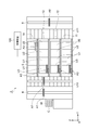
- FIG. 2 is a schematic view showing an example of a coating and developing apparatus.
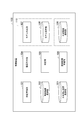
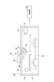
- FIG. 3 is a schematic view showing an example of the inspection unit.
- FIG. 4 is a block diagram showing an example of the functional configuration of the control device.
- FIG. 5 is a block diagram showing an example of the hardware configuration of the control device.
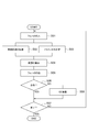
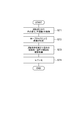
- FIG. 6 is a flow chart showing an example of control (wafer inspection) by the control device.
- FIG. 7 is a diagram showing an example of acquisition positions of spectroscopic spectrum data.
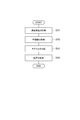
- FIG. 8 is a flow chart showing an example of control by the control device (estimation of the film thickness from the change in color).
- FIG. 1 is a schematic view showing an example of a schematic configuration of a substrate processing system.
- FIG. 2 is a schematic view showing an example of a coating and developing apparatus.
- FIG. 3 is a schematic view showing an example of the inspection unit.
- FIG. 9 is a flow chart showing an example of control by a control device (estimation of film thickness from spectroscopic spectrum data).
- FIG. 10 is a flow chart showing an example of pass / fail judgment.
- FIG. 11 is a flow chart showing an example of control (detailed inspection) by the control device.
- FIG. 12 is a flow chart showing an example of control by the control device (processing of the pattern wafer at the time of model creation).
- FIG. 13 is a flow chart showing an example of control by the control device (processing of the bare wafer at the time of model creation).
- FIG. 14 is a flow chart showing an example of control by a control device (wafer processing at the time of model creation).
- FIG. 15 is a flow chart showing an example of control (model creation) by the control device.
- FIG. 10 is a flow chart showing an example of pass / fail judgment.
- FIG. 11 is a flow chart showing an example of control (detailed inspection) by the control device.
- FIG. 16 is a schematic view showing an example of the inspection unit in the other application example 1.
- FIG. 17 is a perspective view showing an example of a peripherally exposed portion in the inspection unit.
- FIG. 18 is a schematic view showing an example of the inspection unit in the other application example 2.
- FIG. 19 is a schematic view showing an example of the inspection unit in the other application example 3.
- the substrate processing apparatus includes a holding portion that holds a substrate having a film formed on its surface, and an imaging unit that acquires image data by imaging the surface of the substrate held by the holding portion.
- the substrate processing apparatus includes a holding unit that holds a substrate on which a film is formed on the surface, and an imaging unit that images the surface of the substrate held by the holding unit to acquire image data. And a spectroscopic measurement unit that obtains spectroscopic data by dispersing light from the surface of the substrate held by the holding unit.
- the imaging unit acquires an image of the entire surface of the substrate, and the spectroscopic measuring unit disperses light from a plurality of different regions included in the surface of the substrate to obtain spectral data. It can be an aspect to be acquired.
- the spectroscopic measurement unit can acquire spectral data relating to a plurality of different regions included in the surface of the substrate, and thus can acquire information relating to spectral characteristics at a plurality of positions of the substrate. Evaluation can be performed using variations in characteristics. Therefore, the evaluation of the film on the surface of the substrate can be performed in a more multifaceted manner.
- the control unit may control the holding unit, the imaging unit, and the spectroscopic measurement unit. Further, the control unit is different from each other included in the surface of the substrate by the spectroscopic measurement unit in parallel with the image pickup unit imaging the surface of the substrate while moving the holding unit in one direction. It is possible to obtain spectroscopic data by dispersing light from a plurality of regions.
- the control unit can be in a mode of evaluating the film formation state on the surface of the substrate based on the image data captured by the imaging unit.
- the handling of the spectral data can be changed based on the evaluation result of the film formation status based on the image data. it can. Therefore, the image data and the spectral data can be handled more appropriately in the inspection of the substrate.
- It also has a peripheral exposure unit that exposes the peripheral region of the substrate held by the holding unit, and the control unit can also control the peripheral exposure unit.
- the image data obtained by capturing the surface of the substrate can be acquired while being held by the holding portion. Further, by having a configuration capable of acquiring spectral data related to light from the surface, it is possible to accurately evaluate the film formed on the substrate. Further, according to the above configuration, it is possible to evaluate the result of exposure of the peripheral region of the substrate by the peripheral exposure portion.
- the control unit can be configured such that the spectroscopic measurement unit disperses light from a plurality of locations on each of the substrates before and after exposure by the peripheral exposure unit to acquire spectroscopic data.
- the substrate inspection method is a method of inspecting a substrate after film formation, and is an image acquisition step in which the surface of the substrate held by the holding portion is imaged by an imaging unit to acquire image data.
- the spectroscopic measurement step of obtaining spectroscopic data by dispersing light from a part of the region contained in the surface of the substrate held by the holding portion by the spectroscopic measurement unit, and the image data and the spectroscopic data.
- the determination step of determining whether the film meets the acceptance criteria and in the determination step if the film does not satisfy the acceptance criteria, the inspection substrate is subjected to the same film forming process as the substrate.
- Detailed measurement to acquire spectral data by separating the light from the measurement position two-dimensionally dispersed on the surface of the inspection substrate after the film formation held in the film step and the holding portion by the spectral measuring portion. It has steps and.
- the inspection substrate is subjected to a film forming process. ..
- the spectroscopic measurement unit is used to acquire spectroscopic data from the measurement positions dispersed in a two-dimensional manner to perform detailed measurement.
- the film be properly evaluated based on image data and spectroscopic data on a normal substrate, but also detailed inspection when the film does not meet the acceptance criteria can be performed using the same spectroscopic measurement unit. It can be carried out and the evaluation of the membrane can be performed in more detail.
- the image acquisition step while moving the holding portion in one direction, the surface of the substrate is imaged by the imaging unit, and in parallel, the surface of the substrate is imaged by the spectroscopic measurement unit as the spectroscopic measurement step. It is possible to obtain spectral data by dispersing light from a plurality of regions different from each other contained in the above.
- the storage medium is a computer-readable storage medium that stores a program for causing the device to execute the substrate inspection method described above.
- the substrate processing system 1 is a system that forms a photosensitive film, exposes the photosensitive film, and develops the photosensitive film on the substrate.
- the substrate to be processed is, for example, a semiconductor wafer W.
- the substrate processing system 1 includes a coating / developing device 2 and an exposure device 3.
- the exposure apparatus 3 performs an exposure process of a resist film (photosensitive film) formed on the wafer W (substrate). Specifically, the exposure apparatus 3 irradiates the exposed portion of the resist film with energy rays by a method such as immersion exposure.
- the coating / developing apparatus 2 performs a process of forming a resist film on the surface of the wafer W (substrate) before the exposure process by the exposure apparatus 3, and develops the resist film after the exposure process.
- the coating / developing device 2 includes a carrier block 4, a processing block 5, an interface block 6, and a control device 100 (control unit).
- the coating / developing device 2 as the substrate processing apparatus described in the present embodiment corresponds to a substrate inspection system that inspects the film formation status on the substrate. The function as a substrate inspection system will be described later.
- the carrier block 4 introduces the wafer W into the coating / developing device 2 and derives the wafer W from the coating / developing device 2.
- the carrier block 4 can support a plurality of carriers C (accommodation portions) for the wafer W, and incorporates a transfer device A1 including a transfer arm.
- the carrier C accommodates, for example, a plurality of circular wafers W.
- the transport device A1 takes out the wafer W from the carrier C, passes it to the processing block 5, receives the wafer W from the processing block 5, and returns it to the carrier C.
- the processing block 5 has a plurality of processing modules 11, 12, 13, and 14.
- the processing module 11 incorporates a plurality of coating units U1, a plurality of heat treatment units U2, a plurality of inspection units U3, and a transfer device A3 for transporting the wafer W to these units.
- the processing module 11 forms an underlayer film on the surface of the wafer W by the coating unit U1 and the heat treatment unit U2.
- the coating unit U1 of the processing module 11 coats the processing liquid for forming the underlayer film on the wafer W while rotating the wafer W at a predetermined rotation speed, for example.
- the heat treatment unit U2 of the processing module 11 performs various heat treatments accompanying the formation of the underlayer film.
- the heat treatment unit U2 contains, for example, a hot plate and a cooling plate, and heats the wafer W to a predetermined heating temperature by the hot plate, and cools the heated wafer W by the cooling plate to perform heat treatment.
- the inspection unit U3 performs a process for inspecting the surface condition of the wafer W, and acquires, for example, a surface image or information related to the film thickness as information indicating the surface condition of the wafer W.
- the processing module 12 incorporates a plurality of coating units U1, a plurality of heat treatment units U2, a plurality of inspection units U3, and a transfer device A3 for transporting the wafer W to these units.
- the processing module 12 forms an intermediate film on the lower layer film by the coating unit U1 and the heat treatment unit U2.
- the coating unit U1 of the processing module 12 forms a coating film on the surface of the wafer W by coating the treatment liquid for forming an intermediate film on the lower layer film.
- the heat treatment unit U2 of the processing module 12 performs various heat treatments accompanying the formation of the interlayer film.
- the heat treatment unit U2 contains, for example, a hot plate and a cooling plate, and heats the wafer W to a predetermined heating temperature by the hot plate, and cools the heated wafer W by the cooling plate to perform heat treatment.
- the inspection unit U3 performs a process for inspecting the surface condition of the wafer W, and acquires, for example, a surface image or information related to the film thickness as information indicating the surface condition of the wafer W.
- the processing module 13 incorporates a plurality of coating units U1, a plurality of heat treatment units U2, a plurality of inspection units U3, and a transfer device A3 for transporting the wafer W to these units.
- the processing module 13 forms a resist film on the intermediate film by the coating unit U1 and the heat treatment unit U2.
- the coating unit U1 of the processing module 13 coats the treatment liquid for forming the resist film on the intermediate film, for example, while rotating the wafer W at a predetermined rotation speed.
- the heat treatment unit U2 of the processing module 13 performs various heat treatments accompanying the formation of the resist film.
- the heat treatment unit U2 of the processing module 13 forms a resist film by subjecting the wafer W on which the coating film is formed to a heat treatment (PAB: Pre Applied Bake) at a predetermined heating temperature.
- the inspection unit U3 performs a process for inspecting the surface condition of the wafer W, and acquires, for example, information related to the film thickness as information indicating the surface condition of the wafer W.
- the processing module 14 incorporates a plurality of coating units U1, a plurality of heat treatment units U2, and a transfer device A3 for transporting the wafer W to these units.
- the processing module 14 develops the resist film after exposure by the coating unit U1 and the heat treatment unit U2.
- the coating unit U1 of the processing module 14 applies, for example, a developing solution on the surface of the exposed wafer W while rotating the wafer W at a predetermined rotation speed, and then rinses the developing solution with a rinsing solution to form a resist film.
- the heat treatment unit U2 of the processing module 14 performs various heat treatments associated with the development process. Specific examples of the heat treatment include heat treatment before development treatment (PEB: Post Exposure Bake), heat treatment after development treatment (PB: Post Bake), and the like.
- a shelf unit U10 is provided on the carrier block 4 side in the processing block 5.
- the shelf unit U10 is divided into a plurality of cells arranged in the vertical direction.
- a transport device A7 including an elevating arm is provided in the vicinity of the shelf unit U10. The transfer device A7 raises and lowers the wafer W between the cells of the shelf unit U10.
- a shelf unit U11 is provided on the interface block 6 side in the processing block 5.
- the shelf unit U11 is divided into a plurality of cells arranged in the vertical direction.
- the interface block 6 transfers the wafer W to and from the exposure apparatus 3.
- the interface block 6 has a built-in transfer device A8 including a transfer arm, and is connected to the exposure device 3.
- the transport device A8 passes the wafer W arranged on the shelf unit U11 to the exposure device 3, receives the wafer W from the exposure device 3, and returns the wafer W to the shelf unit U11.
- the inspection unit U3 included in the processing modules 11 to 13 will be described.
- the inspection unit U3 acquires information on the surface of the film (underlayer film, intermediate film, or resist film) formed by the coating unit U1 and the heat treatment unit U2, and information on the film thickness.
- the inspection unit U3 includes a housing 30, a holding unit 31, a linear driving unit 32, an imaging unit 33, a light projecting / reflecting unit 34, and a spectroscopic measuring unit 40.
- the holding unit 31 holds the wafer W horizontally.
- the linear drive unit 32 uses an electric motor or the like as a power source to move the holding unit 31 along a horizontal linear path.
- the imaging unit 33 has a camera 35 such as a CCD camera.
- the camera 35 is provided on one end side in the inspection unit U3 in the moving direction of the holding portion 31, and is directed to the other end side in the moving direction.
- the light projecting / reflecting unit 34 projects light into the imaging range and guides the reflected light from the imaging range to the camera 35 side.
- the light projecting / reflecting unit 34 has a half mirror 36 and a light source 37.
- the half mirror 36 is provided at a position higher than the holding portion 31 in the middle portion of the moving range of the linear driving portion 32, and reflects light from below toward the camera 35 side.
- the light source 37 is provided on the half mirror 36, and irradiates the illumination light downward through the half mirror 36.
- the spectroscopic measurement unit 40 has a function of injecting light from the wafer W and dispersing it to acquire a spectroscopic spectrum.
- the spectroscopic measurement unit 40 disperses the incident portion 41 that incidents the light from the wafer W, the waveguide 42 that waveguides the light incident on the incident portion 41, and the light waveguide by the waveguide 42. It has a spectroscope 43 for acquiring a spectroscopic spectrum and a light source 44.
- the incident portion 41 is configured to be capable of incident light from the central portion of the wafer W when the wafer W held by the holding portion 31 moves along with being driven by the linear drive unit 32.
- the spectroscopic measurement unit 40 can acquire the spectral spectrum at each position along the radial direction of the wafer W including the central portion of the wafer W.
- the waveguide 42 is composed of, for example, an optical fiber or the like.
- the spectroscope 43 disperses the incident light and acquires a spectroscopic spectrum including intensity information corresponding to each wavelength.
- the light source 44 irradiates the illumination light downward. As a result, the reflected light from the wafer W enters the spectroscope 43 via the incident portion 41 and the waveguide portion 42.
- the wavelength range of the spectroscopic spectrum acquired by the spectroscope 43 can be, for example, the wavelength range of visible light (380 nm to 780 nm). Therefore, by using a light source that emits visible light as the light source 44 and dispersing the reflected light on the surface of the wafer W with respect to the light from the light source 44 by the spectroscope 43, spectral spectrum data (spectral data) in the wavelength range of visible light (spectral data). ) Can be obtained.
- the wavelength range of the spectroscopic spectrum acquired by the spectroscope 43 is not limited to the range of visible light, and may be, for example, a wavelength range including infrared rays and ultraviolet rays. Appropriate ones can be selected as the spectroscope 43 and the light source 44 according to the wavelength range of the acquired spectroscopic spectrum data.
- the inspection unit U3 operates as follows to acquire image data on the surface of the wafer W.
- the linear drive unit 32 moves the holding unit 31.
- the wafer W passes under the half mirror 36.
- the reflected light from each part of the wafer W surface is sequentially sent to the camera 35.
- the camera 35 forms an image of reflected light from each part of the wafer W surface and acquires image data of the wafer W surface.
- the image data of the wafer W surface captured by the camera 35 changes, for example, the color of the wafer W surface changes according to the film thickness. That is, acquiring the image data of the surface of the wafer W corresponds to acquiring the information relating to the film thickness of the film formed on the surface of the wafer W. This point will be described later.
- the image data acquired by the camera 35 is sent to the control device 100.
- the control device 100 can estimate the film thickness of the film on the surface of the wafer W based on the image data, and the estimation result is held as an inspection result in the control device 100.
- the spectroscopic measurement unit 40 incidents light from the surface of the wafer W to perform spectroscopic measurement.
- the linear drive unit 32 moves the holding unit 31
- the wafer W passes under the incident unit 41.
- the reflected light from each portion of the wafer W surface is incident on the incident portion 41, and is incident on the spectroscope 43 via the waveguide portion 42.
- the incident light is separated by the spectroscope 43, and spectroscopic spectrum data is acquired.
- the film thickness of the film formed on the surface of the wafer W changes, for example, the spectral spectrum changes according to the film thickness.
- acquiring the spectral spectrum data of the surface of the wafer W corresponds to acquiring the information relating to the film thickness of the film formed on the surface of the wafer W. This point will be described later.
- acquisition of image data and spectroscopic measurement can be performed in parallel. Therefore, the measurement can be performed in a short time as compared with the case where these are performed individually.
- the spectroscopic spectrum data acquired by the spectroscope 43 is sent to the control device 100.
- the control device 100 can estimate the film thickness of the film on the surface of the wafer W based on the spectral spectrum data, and the estimation result is held as an inspection result in the control device 100.
- Control device An example of the control device 100 will be described in detail.
- the control device 100 controls each element included in the coating / developing device 2.
- the control device 100 is configured to perform a process process including forming each of the above-mentioned films on the surface of the wafer W and performing a developing process. Further, the control device 100 is configured to execute correction of parameters related to the process processing based on the result of the process processing. Details of these process processes and the like will be described later.
- the control device 100 has an inspection execution unit 101, an image information holding unit 102, a spectroscopic measurement result holding unit 103, a film thickness calculation unit 104, and a determination unit 105 as functional configurations. .. Further, the control device 100 includes a detailed inspection execution unit 106, a model creation unit 107, a model holding unit 108, and a spectroscopic information holding unit 109.
- the inspection execution unit 101 has a function of controlling the operation related to the inspection of the wafer W in the inspection unit U3. As a result of the inspection by the inspection unit U3, image data and spectral spectrum data are acquired.
- the image information holding unit 102 has a function of acquiring and holding image data obtained by imaging the surface of the wafer W from the image capturing unit 33 of the inspection unit U3.
- the image data held by the image information holding unit 102 is used for estimating the film thickness of the film formed on the wafer W.
- the image data may be used not for the evaluation of the film thickness but for the evaluation of the film formation state. This point will also be described later.
- the spectroscopic measurement result holding unit 103 has a function of acquiring and holding spectroscopic spectrum data related to the surface of the wafer W from the spectroscope 43 of the inspection unit U3.
- the spectroscopic spectrum data held by the spectroscopic measurement result holding unit 103 is used for estimating the film thickness of the film formed on the wafer W.
- the film thickness calculation unit 104 calculates the film thickness of the film formed on the wafer W based on the image data held by the image information holding unit 102 and the spectral spectrum data held by the spectral measurement result holding unit 103. Has the function of Details of the procedure for calculating the film thickness will be described later.
- the determination unit 105 has a function of determining whether the film thickness calculated by the film thickness calculation unit 104 is appropriate. Since the formation of the film is performed by the coating unit U1 and the heat treatment unit U2 in the previous stage of the inspection unit U3, this determination corresponds to the determination as to whether or not the coating unit U1 and the heat treatment unit U2 are operating properly.
- the detailed inspection execution unit 106 has a function of performing a detailed inspection for confirming the operation of the coating unit U1 and the heat treatment unit U2 when it is determined that there is a problem with the film thickness as a result of the determination by the determination unit 105.
- the detailed inspection will be described later, but a bare wafer on which a pattern is not formed is prepared as an inspection wafer, a film is formed on the wafer, and the film thickness is evaluated.
- the model creation unit 107 and the model holding unit 108 have a function of creating and holding a model to be used when calculating the film thickness from the image data. Color information on the surface of the wafer W can be acquired from the image data captured by the inspection unit U3. Therefore, the model creating unit 107 creates a model capable of estimating the film thickness based on the color information of the wafer W surface, and the model holding unit 108 holds the created model.
- the film thickness calculation unit 104 estimates the film thickness of the wafer W to be inspected by using the model.
- the spectral information holding unit 109 has a function of holding the spectral information used when calculating the film thickness from the spectral spectral data.
- the spectral spectrum data acquired by the inspection unit U3 varies depending on the type and film thickness of the film formed on the surface of the wafer W. Therefore, the spectral information holding unit 109 holds information related to the correspondence between the film thickness and the spectral spectrum.
- the film thickness calculation unit 104 estimates the film thickness of the wafer W (target substrate) to be inspected based on the information held by the spectroscopic information holding unit 109.
- the control device 100 is composed of one or a plurality of control computers.
- the control device 100 has a circuit 120 shown in FIG.
- the circuit 120 has one or more processors 121, a memory 122, a storage 123, and an input / output port 124.
- the storage 123 has a computer-readable storage medium, such as a hard disk.
- the storage medium stores a program for causing the control device 100 to execute the process processing procedure described later.
- the storage medium may be a removable medium such as a non-volatile semiconductor memory, a magnetic disk, or an optical disk.
- the memory 122 temporarily stores the program loaded from the storage medium of the storage 123 and the calculation result by the processor 121.
- the processor 121 constitutes each of the above-mentioned functional modules by executing the above program in cooperation with the memory 122.
- the input / output port 124 inputs / outputs an electric signal to / from a member to be controlled according to a command from the processor 121.
- each functional module of the control device 100 may be configured by a dedicated logic circuit or an ASIC (Application Specific Integrated Circuit) in which the logic circuit is integrated.
- ASIC Application Specific Integrated Circuit
- the control device 100 may not include all the above functions.
- the model management unit 110 including the model creation unit 107 and the model holding unit 108, or the model creation unit 107 may be provided in the external device.
- these functions may be provided in, for example, a device different from the control device 100 that controls the coating / developing device 2.
- the external device and the control device 100 cooperate with each other to exert the function described in the following embodiment.
- the external device equipped with the function corresponding to the control device 100 described in the present embodiment and the board processing device described in the present embodiment can integrally function as a board inspection system. ..
- control device 100 controls the transfer device A1 so as to transfer the wafer W to be processed in the carrier C to the shelf unit U10, and arranges the wafer W in the cell for the processing module 11.
- the transport device A7 is controlled so as to.
- control device 100 controls the transfer device A3 so as to transfer the wafer W of the shelf unit U10 to the coating unit U1 and the heat treatment unit U2 in the processing module 11. Further, the control device 100 controls the coating unit U1 and the heat treatment unit U2 so as to form an underlayer film on the surface of the wafer W. After forming the underlayer film, the control device 100 may control the transfer device A3 so as to transfer the wafer W to the inspection unit U3, and the inspection unit U3 may be used to inspect the surface condition of the wafer W. .. After that, the control device 100 controls the transfer device A3 so as to return the wafer W on which the underlayer film is formed to the shelf unit U10, and controls the transfer device A7 so as to arrange the wafer W in the cell for the processing module 12. ..
- control device 100 controls the transfer device A3 so as to transfer the wafer W of the shelf unit U10 to the coating unit U1 and the heat treatment unit U2 in the processing module 12. Further, the control device 100 controls the coating unit U1 and the heat treatment unit U2 so as to form an intermediate film on the lower film of the wafer W. For example, the control device 100 controls the coating unit U1 so as to form an intermediate film by applying a treatment liquid for forming an intermediate film on the lower layer film of the wafer W. Next, the control device 100 controls the heat treatment unit U2 so as to perform the heat treatment on the interlayer film.
- the control device 100 controls the transfer device A3 so as to transfer the wafer W to the inspection unit U3, and controls the inspection unit U3 to inspect the surface condition of the wafer W. After that, the control device 100 controls the transfer device A3 so as to return the wafer W to the shelf unit U10, and controls the transfer device A7 so as to arrange the wafer W in the cell for the processing module 13.
- control device 100 controls the transfer device A3 so as to transfer the wafer W of the shelf unit U10 to each unit in the processing module 13, and the coating unit so as to form a resist film on the intermediate film of the wafer W.
- the control device 100 controls the coating unit U1 so as to form a resist film by applying a treatment liquid for forming a resist film on the intermediate film of the wafer W.
- the control device 100 controls the heat treatment unit U2 so as to heat-treat the resist film.
- the control device 100 controls the transfer device A3 so as to transfer the wafer W to the inspection unit U3, and the inspection unit U3 is used to transfer the surface condition of the wafer W (for example, the upper layer film). The film thickness) may be inspected.
- the control device 100 controls the transfer device A3 so as to transfer the wafer W to the shelf unit U11.
- control device 100 controls the transfer device A8 so as to send the wafer W of the shelf unit U11 to the exposure device 3. After that, the control device 100 controls the transfer device A8 so as to receive the exposed wafer W from the exposure device 3 and arrange it in the cell for the processing module 14 in the shelf unit U11.
- control device 100 controls the transfer device A3 so as to transfer the wafer W of the shelf unit U11 to each unit in the processing module 14, and the coating unit U1 and the coating unit U1 and the resist film of the wafer W are developed.
- the heat treatment unit U2 is controlled.
- the control device 100 controls the transfer device A3 so as to return the wafer W to the shelf unit U10, and controls the transfer device A7 and the transfer device A1 so as to return the wafer W to the carrier C. This completes the process process.
- the substrate inspection method is a method related to the inspection of the wafer W after film formation performed in the inspection units U3 provided in the processing modules 11 to 13.
- the inspection unit U3 inspects whether the desired film formation has been performed on the wafer W after the film formation. Specifically, the state and film thickness of the surface of the film formed on the wafer W are evaluated.
- the inspection unit U3 has, for example, an image pickup unit 33 and a spectroscopic measurement unit 40 as described above, the image data obtained by imaging the surface of the wafer W by the image pickup unit 33 and the spectroscopy of the surface of the wafer W by the spectroscopic measurement unit 40. Spectral data can be obtained.
- the control device 100 evaluates the film formation status based on these data.
- the inspection unit U3 can perform an inspection after forming each of the lower layer film, the intermediate film, and the resist film in the processing modules 11 to 13.
- FIG. 6 is a flow chart illustrating a series of flows of the substrate inspection method in the inspection unit U3.
- the control device 100 executes step S01.
- step S01 the wafer W on which the film is formed in the coating unit U1 and the heat treatment unit U2 is carried into the inspection unit U3.
- the wafer W is held by the holding unit 31.
- step S02 image acquisition step
- the surface of the wafer W is imaged by the imaging unit 33.
- the image pickup unit 33 takes an image of the wafer W surface while moving the holding unit 31 in a predetermined direction by driving the linear drive unit 32.
- the image pickup unit 33 acquires image data related to the surface of the wafer W.
- the image data is held in the image information holding unit 102 of the control device 100.
- step S03 the inspection execution unit 101 of the control device 100 executes step S03 (spectral measurement step).
- the spectroscopic measurement unit 40 performs spectroscopic measurement of one line on the surface of the wafer W.
- the incident portion 41 of the spectroscopic measurement unit 40 is provided on the path through which the center of the wafer W held by the holding unit 31 passes when the holding unit 31 moves, the central portion of the wafer W is provided. It is possible to acquire a spectral spectrum at each position along the radial direction of the wafer W including the wafer W. Therefore, as shown in FIG. 7, the incident portion 41 is incident with the reflected light on the surface along the center line L passing through the center of the wafer W.
- the spectroscope 43 measures the spectral spectrum of light incident at predetermined intervals. As a result, the spectrometer 43, as a plurality of locations along the center line L, such as to obtain the spectral data corresponding to n positions of P 1 ⁇ P n shown in FIG. In this way, by using the spectroscope 43, spectroscopic spectrum data relating to the surface of the wafer W at a plurality of locations along the center line L of the wafer W can be acquired. Note that n can be appropriately changed depending on the interval of spectroscopic measurements by the spectroscope 43 and the moving speed of the wafer W by the holding unit 31. The spectroscopic spectrum data acquired by the spectroscope 43 is held by the spectroscopic measurement result holding unit 103 of the control device 100.
- the film thickness calculation unit 104 of the control device 100 executes step S04.
- step S04 the film thickness of the film on the wafer W surface is calculated based on the image data related to the wafer W surface or the spectroscopic spectrum data obtained by spectroscopic measurement.
- the procedure for calculating the film thickness using the image data will be described with reference to FIG.
- the film thickness model created by the model creation unit 107 and held by the model holding unit 108 is used.
- the film thickness model is a film thickness based on information related to a change in color of each pixel in image data obtained by imaging the surface of the wafer W when a predetermined film is formed (color change before and after forming a predetermined film). It is a model for calculating, and is a model showing the correspondence between the information related to the color change and the film thickness.
- the model creation unit 107 of the control device 100 By creating such a model in advance by the model creation unit 107 of the control device 100 and holding it by the model holding unit 108, information on the color change at each position of the image data is acquired, and the color change is obtained.
- the film thickness can be estimated from.
- the method of creating the film thickness model will be described later, but the surface of both the wafer W that has undergone each process up to the previous stage and the wafer W that has formed a predetermined film thereafter are imaged to obtain image data. Get and identify how the color changed.
- the film thickness of the wafer formed under the same conditions is measured. This makes it possible to specify the correspondence between the film thickness and the change in color. By repeating this measurement while changing the film thickness, it is possible to obtain the correspondence between the information related to the color change and the film thickness.
- the method of calculating the film thickness from the image data is as shown in FIG.
- the calculation (estimation) of the film thickness based on the above image data is possible when the film formed on the wafer W is relatively thin (for example, about 500 nm or less), but it is difficult when the film thickness becomes large. This is because as the film thickness increases, the change in color with respect to the change in film thickness decreases, and it becomes difficult to accurately estimate the film thickness from the information related to the change in color. Therefore, when a film having a large film thickness is formed, the film thickness is estimated based on the spectroscopic spectrum data.
- the procedure for calculating the film thickness using the spectral spectrum data utilizes the change in reflectance according to the film thickness of the surface film.
- the light is reflected on the surface of the uppermost film or at the interface between the uppermost film and the lower layer (the film or the wafer). Then, these lights are emitted as reflected light. That is, the reflected light includes light having two components having different phases. Further, as the film thickness of the surface increases, the phase difference increases. Therefore, when the film thickness changes, the degree of interference between the light reflected on the film surface and the light reflected on the interface with the lower layer changes.
- the control device 100 holds in advance information related to the shape of the spectral spectrum according to the film thickness of the film formed on the surface. Then, the spectral spectrum of the reflected light obtained by irradiating the actual wafer W with light is compared with the information held in advance. This makes it possible to estimate the film thickness of the film on the surface of the wafer W. Information related to the relationship between the film thickness and the shape of the spectral spectrum used for estimating the film thickness is held in the spectral information holding unit 109 of the control device 100.
- the method of calculating the film thickness from the spectroscopic spectrum data is as shown in FIG.
- the information that the spectroscopic spectrum data is held by the spectroscopic information holding unit 109, that is, the spectral spectrum corresponding to the theoretical film thickness.
- the film thickness of the region where the spectral spectrum data is obtained can be estimated for each spectral spectrum data (step S23). This makes it possible to estimate the film thickness for each spectral spectrum data, that is, at each position on the wafer W surface.
- the film thickness on the surface of the wafer W can be calculated based on each spectral spectral data. Information on the thickness distribution can be obtained.
- the image data of the wafer W imaged by the imaging unit 33 is an image of the entire surface of the wafer W, it is possible to estimate the film thickness of the entire surface of the wafer W from the image data.
- the location where the spectroscopic spectrum data is acquired is limited to the center line L of the wafer W. Therefore, in estimating the film thickness of the wafer W surface based on the spectral spectrum data, it is difficult to evaluate the overall film thickness distribution as compared with the estimation of the film thickness based on the image data.
- the estimation of the film thickness based on the image data is limited to the case where the film formed on the wafer W is thin to some extent.
- the film thickness can be estimated based on the spectral spectrum data not only when the film formed on the wafer W is thick to some extent, but also when the film thickness is small (for example, several tens of nm). is there.
- the estimation of the film thickness based on the spectral spectrum data is not limited to the thickness of the wafer W, and is therefore considered to be highly versatile.
- a predetermined pattern is formed on the wafer W. Therefore, there is a possibility that spectroscopic spectrum data affected by the unevenness of the pattern can be obtained.
- the spectroscopic spectrum data acquired from the wafer W may not always accurately reflect the film thickness of the film formed on the wafer W. It is necessary to handle the spectroscopic spectrum data in consideration of this point. It is also necessary to consider that the film thickness estimated from the spectroscopic spectrum data may not be accurate. However, this problem can be solved if the position where the spectroscopic spectrum data is acquired can be specified more accurately. That is, when the spectral spectrum relating to the surface of the patterned wafer W can be acquired, the accuracy derived from the pattern can be controlled so that the spectral spectrum data can be acquired at a position different from the position where the step is formed. Can be avoided.
- the image data can be used, for example, for evaluating the film formation status.
- the evaluation of the film formation status is to check whether there is any abnormality that can be detected from the image data such as whether there is a defect such as a spot on the film surface. Therefore, by acquiring both the image data and the spectroscopic spectrum data, the film formation state can be evaluated in more detail. For example, it is assumed that a defect can be detected from the image data in a part of the region on the center line L of the wafer W for which the spectral spectrum data is to be acquired.
- the accuracy of the estimated value can be improved by specifying the spectral spectrum data of the portion overlapping or adjacent to the region and not using the spectral spectrum data for calculating the average value of the film thickness estimation. It is also possible to automatically associate and store the image corresponding to the defective region and the estimated film thickness based on the spectral spectrum data of the region. As a result, information in the depth direction in the plane region where the defect has occurred can be easily and surely taken out, so that, for example, the efficiency and high accuracy of the work of analyzing the state of the defect and the reason for the occurrence after the fact can be improved. In this way, the spectral spectrum data can be widely utilized according to the film forming condition obtained from the image data by the configuration in which the film forming condition on the surface of the substrate is evaluated based on the image data.
- the acquisition of the spectral spectrum data (step S03) may be omitted.
- the spectroscopic spectrum data itself may not be performed by the spectroscopic measurement unit 40, and the film thickness may be estimated and the film formation status may be evaluated based only on the image data.
- step S05 the inspection execution unit 101 of the control device 100 executes step S05.
- the wafer W is carried out from the inspection unit U3.
- the carried-out wafer W is sent to, for example, a processing module in a subsequent stage.
- step S06 determineation step.
- step S06 it is confirmed whether the film thickness of the wafer W has reached the acceptance standard.
- the acceptance criterion is based on whether or not the film thickness of the entire wafer W is included in the predetermined film thickness setting range. That is, in step S06, it is evaluated whether or not the film formation is properly performed in the coating unit U1 and the heat treatment unit U2 in the previous stage.
- a set value (setting range) of the film thickness is set for each film formed on the wafer W.
- the film thickness setting range D is shown, and the estimation results of the film thicknesses of the plurality of wafers W are shown as dots in time series.
- the film thickness at a plurality of locations on the surface of one wafer W is estimated based on both the image data and the spectroscopic spectrum data.
- FIG. 10 it is assumed that the estimation result of the average value of the film thicknesses at a plurality of locations on one wafer W is shown.
- one wafer W for performing the same substrate processing is sampled for estimation for each lot (25 sheets) is shown, but the present invention is not limited to this, and for example, 10 wafers are processed. It may be a unit such as one sheet for each sheet and one sheet for each hour.
- the setting range D includes the estimation results of the film thickness at all the locations related to the plurality of wafers W processed in chronological order, it is determined that the wafer W is acceptable. be able to.
- the estimation result of the film thickness outside the set range D appears, it can be determined that the acceptance criteria are reached and within.
- a configuration that considers the bias of the film thickness may be used as a pass criterion. For example, in the case of estimating the film thickness from the spectroscopic spectrum data, as shown by the solid line X2 or the solid line X3 in FIG. 10, the estimation results of a plurality of film thicknesses processed along the time series gradually deviate from the set range D.
- the result is changing as follows.
- the criteria (passing criteria) for determining the pass / fail of the film thickness in step S06 may be appropriately changed according to the change status in the time series.
- step S07 it is determined whether or not the inspection related to the next wafer W is to be performed, and whether the inspection is completed (S07-YES) or the inspection related to the next wafer W is started (S07-NO).
- Step S08 is a detailed inspection (QC inspection) related to the film thickness.
- the detailed inspection is an inspection using a bare wafer (wafer whose surface is not patterned or the like) called a QC wafer (inspection substrate).
- a detailed inspection is performed in which the QC wafer is carried into the coating unit U1 and the heat treatment unit U2, film formation is performed under the same conditions as the normal wafer, and then the inspection unit U3 evaluates the film thickness in more detail than the normal wafer. That is.
- This detailed inspection is particularly useful when estimating the film thickness using spectroscopic spectrum data in a normal wafer W.
- the film thickness is evaluated using the spectral spectrum data in the inspection relating to the ordinary wafer W, the film thickness distribution on the entire surface of the wafer W is not evaluated for the ordinary wafer W. Therefore, when it is determined in the pass / fail determination (step S06) that the wafer W has failed, it is necessary to grasp what kind of film thickness is in the region where the film thickness is not estimated.
- the detailed inspection corresponds to this inspection.
- step S31 the detailed inspection execution unit 106 of the control device 100 executes step S31.
- the QC wafer that has been film-formed by the coating unit U1 and the heat treatment unit U2 is carried into the inspection unit U3. That is, the QC wafer is carried into the inspection unit U3 after the film forming process is performed under the same conditions as the wafer W which is the target substrate (deposition step).
- the carried-in QC wafer is held by the holding unit 31.
- step S32 the film thickness is measured at various places in the plane.
- spectroscopic spectrum data is acquired at multiple points. The points for measuring the film thickness are dispersed over the entire surface of the QC wafer.
- a plurality of spectra are dispersed along the center line L of the wafer W in accordance with the movement of the holding portion 31 in one direction. The spectrum data is acquired.
- the holding portion 31 is moved while changing the orientation of the QC wafer held by the holding portion 31.
- the inspection unit U3 can be used to acquire spectral spectrum data at various measurement positions dispersed and arranged two-dimensionally on the wafer surface.
- step S33 the film thickness of the wafer W surface is calculated based on each of the plurality of spectral spectrum data related to the wafer W surface, and the in-plane film thickness distribution is calculated.
- the procedure for calculating the film thickness using the spectroscopic spectrum data can be the same as the method for calculating the film thickness of the normal wafer W, and is specifically as shown in FIG.
- step S34 the detailed inspection execution unit 106 of the control device 100 executes step S34.
- the QC wafer is carried out from the inspection unit U3.
- the carried-out wafer W is sent to, for example, a processing module in a subsequent stage.
- step S35 it is confirmed whether the film thickness of the wafer W has reached the acceptance standard.
- the acceptance criteria here is based on whether or not the film thickness distribution measured on the surface of the QC wafer is included in the predetermined film thickness setting range. That is, in step S33, the coating unit U1 and the heat treatment unit U2 in the previous stage evaluate whether or not the film is properly formed on the entire wafer surface.
- the detailed inspection execution unit 106 of the control device 100 ends a series of processes.
- the pass / fail judgment regarding the film thickness distribution is unsuccessful (S35-NO)
- the detailed inspection execution unit 106 of the control device 100 does not properly perform the film formation by transmitting an error message or the like. Is notified to the operator and the like.
- the cause of the improper film thickness is investigated (step S36), and the portion related to the cause is adjusted (step S37).
- the QC wafer is introduced again (step S31) and a series of detailed inspections are performed.
- the investigation of the cause (step S37) and the adjustment (step S38) may be performed independently by the control device 100. Further, for example, these steps may be performed by the operator of the control device 100 (board processing system 1) or the like operating the control device 100 so that the control device 100 only notifies an error.
- step S35 The detailed inspection (QC inspection) is repeated until the pass / fail judgment (step S35) relating to the in-plane distribution of the film thickness on the wafer surface is passed.
- the pass / fail determination (step S35) it can be said that the film formation related to the normal wafer W can be restarted. That is, as shown in FIG. 6, when the processing is not completed (S07-NO), the inspection in which the normal wafer W is carried in can be restarted.
- the film thickness model associates the film thickness with the correspondence between the color information of the image data. Therefore, with respect to the wafer W having a known film thickness, the correspondence between the film thickness and the color information can be obtained by specifying the color information from the image data obtained by imaging the wafer W. In order to accurately measure the film thickness when a film is formed on a wafer, the film thickness when a film is formed on a wafer (bare wafer) that has not been patterned is measured by cross-sectional measurement or the like. Is required to do.
- the film thickness information and color information used in the film thickness model are acquired.
- the unpatterned bare wafer (color information substrate) used for acquiring color information and the unpatterned bare wafer (film thickness measurement substrate) used for measuring the film thickness are used. And are used.
- step S41 the color information substrate is prepared.
- a bare wafer is prepared as a color information substrate as described above. Further, by imaging the bare wafer used as the color information substrate at this stage in the inspection unit U3, the image data related to the substrate before the film formation is acquired. The image data obtained at this time is used to acquire color information on the surface of the wafer after forming the underlayer film.
- step S42 the lower layer film is formed on the prepared color information substrate by controlling each unit of the processing module 11.
- the underlayer film is formed with a predetermined setting.
- step S43 by controlling the inspection unit U3 of the processing module 11, image data related to the surface of the color information substrate on which the underlayer film is formed is acquired.
- the image data obtained at this time is used to acquire color information on the surface of the wafer after forming the underlayer film.
- step S44 an intermediate film is formed on the lower layer film of the color information substrate by controlling each unit of the processing module 12.
- the interlayer film is formed with a predetermined setting.
- step S45 by controlling the inspection unit U3 of the processing module 12, image data relating to the surface of the color information substrate on which the interlayer film is formed is acquired. The image data obtained at this time is used to acquire color information on the surface of the wafer after the interlayer film is formed.
- step S46 a resist film is formed on the intermediate film of the color information substrate by controlling each unit of the processing module 13.
- the interlayer film is formed with a predetermined setting.
- step S47 by controlling the inspection unit U3 of the processing module 13, image data related to the surface of the color information substrate on which the resist film is formed is acquired. The image data obtained at this time is used to acquire color information on the surface of the wafer after the resist film is formed.
- the underlayer film, the interlayer film, and the resist film are formed in the same manner as in the substrate processing step related to the actual wafer W, and image data is acquired every time the film is formed. Do. As a result, it is possible to acquire image data of the surface of the color information substrate manufactured under the same conditions as when the wafer W is formed.
- the film thickness measuring substrate is used to accurately calculate the film thickness formed on the wafer when the film is formed under predetermined conditions. Therefore, when three types of films, a lower layer film, an intermediate film, and a resist film, are formed on a wafer, a bare wafer in which no other film is formed on the lower layer is used when forming each film. As a result, the film thickness can be accurately measured without being affected by a slight change in the film thickness due to the provision of another film in the lower layer.
- step S51 the film thickness measurement substrate is prepared.
- the film thickness measurement substrate is a wafer whose surface is not patterned or the like.
- a plurality of substrates for film thickness measurement are prepared according to the number of subsequent film formations.
- step S52 the model creation unit 107 of the control device 100 executes step S52.
- the lower layer film is formed on the prepared film thickness measurement substrate by controlling each unit of the processing module 11.
- the underlayer film is formed with the same settings (predetermined settings) as those of the color information substrate.
- step S53 by controlling the inspection unit U3 of the processing module 11, image data relating to the surface of the film thickness measurement substrate on which the underlayer film is formed is acquired.
- the image data of the bare wafer obtained at this time may be used when creating a model of color information of the surface of the wafer after forming the underlayer film.
- step S54 an interlayer film is formed on the film thickness measuring substrate by controlling each unit of the processing module 12.
- the interlayer film is formed with the same settings (predetermined settings) as those of the color information substrate.
- the film is formed on a bare wafer on which nothing is formed.
- step S55 by controlling the inspection unit U3 of the processing module 12, image data relating to the surface of the film thickness measurement substrate on which the interlayer film is formed is acquired.
- the image data obtained at this time may be used when creating a model of color information on the surface of the wafer after the interlayer film is formed.
- step S56 a resist film is formed on the film thickness measuring substrate by controlling each unit of the processing module 12.
- the resist film is formed with the same settings (predetermined settings) as those of the color information substrate.
- the film is formed on a bare wafer on which nothing is formed.
- step S57 by controlling the inspection unit U3 of the processing module 12, image data relating to the surface of the film thickness measurement substrate on which the resist film is formed is acquired.
- the image data obtained at this time may be used when creating a model of color information on the surface of the wafer after forming the resist film.
- the film thickness of the underlayer film, the interlayer film, and the resist film which is performed on the actual wafer W, is individually formed on different bare wafers. Therefore, a plurality of substrates for film thickness measurement are prepared according to the number of film forming steps.
- step S58 the film thickness is measured for each of the film thickness measurement substrate on which the lower layer film is formed, the film thickness measurement substrate on which the intermediate film is formed, and the film thickness measurement substrate on which the resist film is formed.
- the film thickness can be measured by using the spectroscopic measurement unit 40 described above. That is, as described above, the film thickness can be calculated using the spectral spectrum data by utilizing the change in the reflectance according to the film thickness of the surface film. That is, the reflected light from the wafer used for acquiring the spectral spectrum data includes light having a component having a phase difference different depending on the film thickness.
- the film thickness can be accurately calculated from the spectral spectrum data obtained by imaging the film thickness measuring substrate on which the film thickness is formed.
- the calculation of the film thickness from the spectroscopic spectrum data is the same as the method described with reference to FIG.
- a lower layer film is formed on the color information substrate (step S61), and at the same time or after that, a lower layer film is formed on the film thickness measurement substrate (step S62). Further, at the same time as or after forming the intermediate film on the color information substrate on which the underlayer film is formed (step S63), the intermediate film is formed on the film thickness measuring substrate (step S64). Further, at the same time as or after forming the resist film on the color information substrate on which the interlayer film is formed (step S65), the resist film is formed on the film thickness measurement substrate (step S66). In this way, by making the film formation timing for the color information substrate and the film thickness measurement substrate as close as possible, both the color information substrate and the film thickness measurement substrate can be formed under closer conditions.
- the film formation timing for the color information substrate and the film formation timing for the film thickness measurement substrate are close to each other. For example, after the treatment liquid is applied to the color information substrate by the coating unit U1, the treatment liquid is applied to the film thickness measurement substrate by the coating unit U1. Then, after the heat treatment of the color information substrate by the heat treatment unit U2, the heat treatment of the film thickness measurement substrate is performed by the heat treatment unit U2. In this way, the film formation timing can be approached by alternately performing the processing in each unit between the color information substrate and the film thickness measurement substrate.
- a film thickness model can be created by combining the data obtained in the above procedure.
- the procedure for creating the film thickness model by the model creation unit 107 of the control device 100 will be further described with reference to FIG.
- step S71 imaging step
- step S41 the image data captured in the preparation stage (step S41) of the color information substrate
- step S43 the image data captured after the lower layer film is formed
- step S58 the film thickness measuring substrate on which the underlayer film is formed under the same film thickness conditions
- step S73 model creation step. That is, a plurality of types of combinations of the film thickness and the color information in a state where the film thickness conditions are changed to change the film thickness (for example, 90 nm, 95 nm, 100 nm, 110 nm) are prepared. By preparing a plurality of combinations in this way, it is possible to specify a relational expression or the like that specifies how the color information changes in response to a change in film thickness.
- step S74 model creation step.
- a film thickness model can be created for the intermediate film and the resist film by following the same procedure.
- the color information substrate is a bare wafer
- a pattern wafer having a pattern corresponding to the target wafer W may be used as the color information substrate.
- the color information obtained by imaging the color information substrate will be closer to the actual wafer W.
- Peripheral exposure may be added to the inspection unit U3 described in the above embodiment to perform peripheral exposure on the wafer W.
- the inspection unit U4 that can be included in the processing module 12 will be described as an example.
- the inspection unit U4 includes a housing 30, a holding unit 31, a linear driving unit 32, an imaging unit 33, a light projecting / reflecting unit 34, a spectroscopic measuring unit 40, and a peripheral exposure unit. Has 80 and.
- the housing 30, the holding part 31, the linear drive part 32, the imaging part 33, the light projecting / reflecting part 34, and the spectroscopic measuring part 40 are the above-mentioned inspection unit U3. It has the same configuration as. Therefore, detailed description thereof will be omitted.
- the peripheral exposure unit 80 is mentioned as a configuration not included in the inspection unit U3.
- the peripheral exposure unit 80 is configured to irradiate the peripheral region Wd (see FIG. 17) of the wafer W on which the resist film is formed with ultraviolet rays to expose a portion of the resist film located in the peripheral region Wd. There is.
- the peripheral exposure unit 80 is located above the holding unit 31.
- the peripheral exposure unit 80 includes a light source 81, an optical system 82, a mask 83, and an actuator 84.
- the light source 81 irradiates the resist film on the wafer W with energy rays (for example, ultraviolet rays) containing an exposed wavelength component toward the lower side (holding portion 31 side).
- energy rays for example, ultraviolet rays
- the light source 81 for example, an ultra-high voltage UV lamp, a high-voltage UV lamp, a low-voltage UV lamp, an excimer lamp, or the like may be used.
- the optical system 82 is located below the light source 81.
- the optical system 82 is composed of at least one lens.
- the optical system 82 converts the light from the light source 81 into substantially parallel light and irradiates the mask 83.
- the mask 83 is located below the optical system 82.
- the mask 83 is formed with an opening 83a for adjusting the exposure area.
- the parallel light from the optical system 82 passes through the opening 83a and irradiates the peripheral region of the surface Wa of the wafer W held by the holding fine 31.
- the actuator 84 is connected to the light source 81.
- the actuator 84 is, for example, an elevating cylinder, and elevates the light source 81 in the vertical direction. That is, the light source 81 has a first height position (lowering position) that approaches the wafer W held by the holding portion 31 and a second height that moves away from the wafer W held by the holding portion 31 by the actuator 84. It is possible to move to and from the vertical position (elevation position).
- the above inspection unit U4 can also be controlled by the control device 100.
- each part other than the peripheral exposure part 80 has the same function as the inspection unit U3.
- the wafer W is held by the holding unit 31, and the wafer W is rotated at a predetermined position at a predetermined rotation speed (for example, about 30 rpm).
- the control device 100 controls the peripheral exposure unit 80 to irradiate the resist film R located in the peripheral region Wd of the surface Wa of the wafer W with a predetermined energy ray (ultraviolet ray) from the light source 81.
- a predetermined energy ray ultraviolet ray
- the control device 100 drives the holding unit 31, the linear driving unit 32, the imaging unit 33, the light projecting / reflecting unit 34, and the spectroscopic measuring unit 40 to drive the wafer W before and after peripheral exposure.
- the surface of the wafer W can be inspected in the same manner as the inspection unit U3.
- the inspection unit U5 includes a housing 30, a holding unit 31, a linear driving unit 32, an imaging unit 33, a light projecting / reflecting unit 34, and a peripheral exposure unit 80.
- Each part of the inspection unit U5 has the same configuration as the above-mentioned inspection unit U4. Therefore, detailed description thereof will be omitted.
- the control device 100 drives the holding unit 31, the linear driving unit 32, the imaging unit 33, and the light projecting / reflecting unit 34 to drive the wafer W before and after the peripheral exposure in the same manner as the inspection unit U4.
- the surface of the wafer W can be inspected. That is, the imaging operation in step S02 of FIG. 6 and the film thickness calculation of FIG. 8 can be performed.
- the inspection unit U6 includes a housing 30, a holding unit 31, a linear driving unit 32, a spectroscopic measuring unit 40, and a peripheral exposure unit 80.
- Each part of the inspection unit U5 has the same configuration as the above-mentioned inspection unit U4. Therefore, detailed description thereof will be omitted.
- the control device 100 inspects the surface of the wafer W before and after the peripheral exposure in the same manner as the inspection unit U4. It can be performed. That is, an operation other than the imaging operation in step S02 of FIG. 6 can be performed.
- the inspection unit U4 of the other application example 1 and the inspection unit U6 of the application example 3 function as a peripheral exposure unit using the peripheral exposure unit 80 for the product wafer W, and use the spectroscopic measurement unit 40 for the QC wafer. It may be made to function as an inspection unit.
- the timing of the QC wafer inspection is not limited to the case where a rejected wafer as shown in step S08 of FIG. 6 occurs, and may be any timing.
- the wafer W is once transported from the inspection unit U5 to the coating unit U1 for development processing, and the inspection unit U5 inspects the developed wafer W again. It may be.
- the holding portion 31 for holding the substrate on which the film is formed on the surface and the surface of the substrate held by the holding portion 31 are imaged. It has an imaging unit 33 that acquires image data, and a spectroscopic measurement unit 40 that disperses light from the surface of a substrate held by the holding unit 31 and acquires spectroscopic data.
- the state of the film has been evaluated from the image data obtained by imaging the surface of the substrate.
- the state of the film cannot be appropriately evaluated from the image data alone.
- it is conceivable to provide a new inspection unit or the like for evaluating the state of the film but there is a possibility that the processing related to the evaluation of the film will increase and the amount of work related to the substrate processing will also increase.
- the inspection unit U3 is configured to acquire image data and spectral data, so that the evaluation of the film on the substrate can be accurately evaluated without providing a new unit or the like. It can be carried out.
- the inspection unit U3 since it is possible to perform evaluation using spectroscopic data, it is possible to accurately evaluate a substrate on which a film with a film thickness is formed, which is difficult to evaluate appropriately using only image data. it can.
- the imaging unit 33 acquires an image of the entire surface of the substrate, and the spectroscopic measuring unit 40 disperses light from a plurality of different regions included in the surface of the substrate to acquire spectral data. Can be.
- the spectroscopic measurement unit can acquire spectral data relating to a plurality of different regions included in the surface of the substrate, and thus can acquire information relating to spectral characteristics at a plurality of positions of the substrate. Evaluation can be performed using variations in characteristics. Therefore, the evaluation of the film on the surface of the substrate can be performed in a more multifaceted manner.
- the substrate processing device further includes a control device 100 as a control unit that controls the holding unit 31, the imaging unit 33, and the spectroscopic measurement unit 40, and the control unit moves the holding unit 31 in one direction.
- a control device 100 as a control unit that controls the holding unit 31, the imaging unit 33, and the spectroscopic measurement unit 40, and the control unit moves the holding unit 31 in one direction.
- the spectroscopic measurement unit 40 disperses light from a plurality of different regions contained in the surface of the substrate and acquires spectroscopic data in parallel with the image pickup unit 33 imaging the surface of the substrate while moving the substrate. There is.
- the image data can be acquired by the imaging unit 33 and the spectroscopic data can be acquired by the spectroscopic measurement unit 40 at the same time while the holding unit 31 is moved in one direction. Therefore, it is possible to prevent the required time from becoming long even though both the image data and the spectroscopic data are acquired, and the image data and the spectroscopic data can be acquired efficiently.
- control device 100 can be configured to evaluate the film formation state on the surface of the substrate based on the image data captured by the image pickup unit 33.
- the handling of the spectral data can be changed based on the evaluation result of the film formation status based on the image data. it can. Therefore, the image data and the spectral data can be handled more appropriately in the inspection of the substrate.
- the peripheral exposure unit 80 for exposing the peripheral region may be further provided. Even in this case, the image data obtained by imaging the surface of the substrate can be acquired while being held by the holding unit 31, and the spectral data related to the light from the surface can be acquired. It is possible to accurately evaluate the film formed on the top. Further, since it is not necessary to separately provide a peripheral exposure unit, it is possible to suppress an increase in the size of the apparatus.
- control device 100 may obtain spectroscopic data by spectroscopically separating light from a plurality of locations on each of the substrates before and after exposure by the peripheral exposure unit by the spectroscopic measurement unit 40. Good. As a result, the labor and time for transporting the substrate can be saved as compared with the case where the peripheral exposure unit is separately provided, and the throughput can be improved as a whole.
- the substrate inspection method described in the above embodiment is a substrate inspection method after film formation, and is an image acquisition step in which the surface of the substrate held by the holding portion is imaged by the imaging unit to acquire image data. Then, the film is formed based on the spectroscopic measurement step of separating the light from a part of the region contained in the surface of the substrate held by the holding portion by the spectroscopic measuring unit and acquiring the spectroscopic data, and the image data and the spectroscopic data.
- the determination step of determining whether or not the acceptance criteria are satisfied and in the determination step, if the film does not meet the acceptance criteria, the inspection substrate is subjected to the same film formation process as the substrate, and is held by the holding portion. It has a detailed measurement step of acquiring spectral data by separating the light from the measurement positions dispersed in two dimensions on the surface of the inspection substrate after the film formation by the spectral measurement unit.
- the inspection substrate is subjected to the film formation process, and the inspection substrate after the film formation is measured from the measurement positions dispersed in two dimensions using the spectroscopic measurement unit.
- the spectroscopic data of the above is acquired and detailed measurement is performed.
- the film be properly evaluated based on image data and spectroscopic data on a normal substrate, but also detailed inspection when the film does not meet the acceptance criteria can be performed using the same spectroscopic measurement unit. It can be carried out and the evaluation of the membrane can be performed in more detail.
- the surface of the substrate is imaged by the imaging unit while moving the holding unit in one direction.
- the spectroscopic measurement unit can disperse light from a plurality of different regions included in the surface of the substrate to acquire spectroscopic data.
- the image data can be acquired by the imaging unit 33 and the spectroscopic data can be acquired by the spectroscopic measurement unit 40 at the same time while the holding unit 31 is moved in one direction. Therefore, it is possible to prevent the required time from becoming long even though both the image data and the spectroscopic data are acquired, and the image data and the spectroscopic data can be acquired efficiently.
- the coating / developing apparatus 2 as the substrate inspection system according to the present embodiment, the surface of the color information substrate provided on the substrate processing apparatus and subjected to the same patterning as the target substrate and having a film formed on the surface thereof. It has an image pickup unit 33 that takes an image and acquires image data. Further, in the coating / developing apparatus 2, a film thickness measuring unit (spectral measuring unit 40) for measuring the film thickness of the film thickness measuring substrate provided on the substrate processing apparatus and having a film formed on the surface under the same conditions as the color information substrate. ). Further, the correspondence between the information related to the change in the surface color of the color information substrate due to the formation of the film obtained based on the image data and the film thickness of the film thickness measurement substrate measured by the film thickness calculation unit 104. It has a model creation unit 107 for creating a film thickness model according to the above.
- the substrate inspection method is a substrate inspection method in a substrate inspection system including a substrate processing apparatus for forming a film on a target substrate.
- the substrate processing apparatus includes an imaging step of acquiring image data by imaging the surface of a color information substrate having the same patterning as the target substrate and having a film formed on the surface.
- the substrate processing apparatus includes a film thickness measuring step of measuring the film thickness of the film thickness measuring substrate having a film formed on the surface under the same conditions as the color information substrate.
- a film thickness model related to the correspondence between the information related to the color change on the surface of the color information substrate due to the formation of the film obtained based on the image data and the film thickness measured in the film thickness measurement step is created. Has a model creation step to do.
- the above-mentioned substrate inspection system and substrate inspection method information on the change in surface color is acquired based on the image data of the surface of the substrate for color information, and for film thickness measurement formed under the same conditions.
- the film thickness of the substrate is measured by the spectral measurement unit 40 as the film thickness measuring unit. Then, by combining these information, a film thickness model related to the correspondence between the information related to the color change and the film thickness is created. Therefore, a model for calculating the film thickness of the film related to the target substrate can be created more easily.
- the film thickness of the film formed on the film thickness measurement substrate is based on the inspection result (spectral data by the spectroscopic measurement unit 40) in the inspection unit U3.
- the film thickness can be specified by the calculation unit 104. Specifically, it is possible to calculate the film thickness from the spectroscopic data using the spectroscopic measurement unit 40.
- the model creation unit 107 of the control device 100 can create a model by combining these. That is, since it is possible to create a model used for calculating the film thickness of the target substrate by using the inspection result in the inspection unit U3 in the substrate processing apparatus, it is possible to create the model more easily than in the past. It will be possible.
- the imaging unit 33 takes an image of the target substrate on which the film is formed on the surface, acquires the image data related to the target substrate, and relates to the change in the surface color of the target substrate due to the formation of the film obtained from the image data related to the target substrate. It is possible to further have a film thickness calculation unit 104 that estimates the film thickness of the target substrate based on the information and the film thickness model.
- an image of the target substrate having a film formed on the surface is imaged to acquire image data related to the target substrate, and information related to a change in the surface color of the target substrate due to the formation of the film obtained from the image data related to the target substrate is obtained. It is possible to further have a film thickness calculation step for estimating the film thickness of the target substrate based on the film thickness model.
- the target is based on the information related to the color change of the surface of the target substrate due to the formation of the film obtained from the image data related to the target substrate in the film thickness calculation unit 104, and the film thickness model.
- the film thickness of the substrate is estimated. Therefore, the film thickness of the target substrate using the model obtained above can also be preferably performed.
- the substrate inspection system further includes a coating unit U1 and a heat treatment unit U2 as a film forming portion that performs a plurality of processes for forming a film on each surface of the color information substrate and the film thickness measurement substrate.
- the film-forming unit may be in a mode in which the process of forming a film on the color information substrate and the process of forming the film on the film thickness measuring substrate are alternately performed.
- the process for forming the film on the color information substrate and the film thickness measurement substrate can be alternately performed.
- the processing on these substrates is alternately performed to obtain the color information substrate and the film thickness measurement substrate.
- the film formation for both can be carried out under closer conditions. Therefore, it is possible to associate the information related to the color change obtained from the color information substrate with the film thickness obtained from the film thickness measurement substrate with higher accuracy, and thus create a model with higher accuracy. can do.
- the film thickness measurement substrate can be a substrate having a flat surface.
- the film thickness can be measured by the film thickness measuring unit. Since the measurement can be performed with higher accuracy, a model with higher accuracy can be created.
- the imaging unit 33 and the spectroscopic measuring unit 40 as the film thickness measuring unit can be provided in the same unit.
- the imaging step and the film thickness measurement step can be performed in parallel.
- the imaging unit 33 and the spectroscopic measurement unit 40 are provided in the same unit as in the inspection unit U3 described in the above embodiment, an apparatus configuration for creating a simple model is realized while preventing the apparatus from becoming large. can do. Further, by performing the imaging step and the film thickness measurement step in parallel, the processing time can be shortened.
- the film thickness measuring unit for creating a model is a unit different from the imaging unit 33. It may be provided in.
- the method of measuring the film thickness is not limited to the acquisition of the above spectroscopic spectrum data.
- a unit for measuring the film thickness is provided separately from the inspection unit U3, and when creating a model, the unit for measuring the film thickness is used to determine the film thickness of the film thickness measurement substrate. It may be configured to perform such a measurement.
- the film thickness may be estimated and evaluated based on the image data acquired by the inspection unit U3.
- the inspection unit U3 is provided in each of the processing modules 11, 12, and 13 has been described.
- the inspection unit U3 is not provided in each module, but may be provided independently of each module.
- the film formed by the above processing modules 11, 12, and 13 is an example, and is appropriately changed.
- a film may be formed above the resist film. That is, the film inspection method described in this embodiment is not limited to the type and number of films, and can be applied to various films formed on a substrate.
- the spectroscopic measurement unit 40 is provided at only one location along the center line L of the wafer W, but the spectroscopic measurement unit 40 is provided along a line different from the center line L. It may be provided. However, when the spectroscopic measurement unit 40 is provided at a position corresponding to the center line L of the wafer W when the wafer W moves with the movement of the holding unit 31, a plurality of regions are provided along the center line L of the wafer W. Spectral spectrum data can be obtained at. Therefore, it is possible to obtain spectral spectrum data in a wider range even though the spectral measurement is performed along one line. Further, a plurality of spectroscopic measurement units 40 may be provided. Although the case where the spectroscopic spectrum data is acquired by the spectroscopic measurement unit 40 has been described, the spectroscopic data acquired by the spectroscopic measurement unit 40 does not have to be the spectral data.
- Substrate processing system 2 ... Coating / developing device (board inspection system), 3 ... Exposure device, 4 ... Carrier block, 5 ... Processing block, 6 ... Interface block, 11-14 ... Processing module, 30 ... Housing, 31 ... holding unit, 32 ... linear drive unit, 33 ... imaging unit, 34 ... reflecting unit, 35 ... camera, 36 ... half mirror, 37 ... light source, 40 ... spectroscopic measuring unit, 41 ... incident unit, 42 ... waveguide unit , 43 ... Spectrometer, 44 ... Light source, 80 ... Peripheral exposure unit, 100 ... Control device, 101 ... Inspection execution unit, 102 ... Image information holding unit, 103 ... Spectral measurement result holding unit, 104 ... Film thickness calculation unit, 105 ... Judgment unit, 106 ... Detailed inspection execution unit, 107 ... Model creation unit, 108 ... Model holding unit, 109 ... Spectral information holding unit.
Landscapes
- Physics & Mathematics (AREA)
- General Physics & Mathematics (AREA)
- Chemical & Material Sciences (AREA)
- Pathology (AREA)
- Immunology (AREA)
- General Health & Medical Sciences (AREA)
- Biochemistry (AREA)
- Analytical Chemistry (AREA)
- Health & Medical Sciences (AREA)
- Life Sciences & Earth Sciences (AREA)
- Engineering & Computer Science (AREA)
- Spectroscopy & Molecular Physics (AREA)
- Theoretical Computer Science (AREA)
- Mathematical Physics (AREA)
- Computer Vision & Pattern Recognition (AREA)
- Quality & Reliability (AREA)
- Multimedia (AREA)
- Signal Processing (AREA)
- Testing Or Measuring Of Semiconductors Or The Like (AREA)
- Length Measuring Devices By Optical Means (AREA)
- Investigating Or Analysing Materials By Optical Means (AREA)
- Investigating Materials By The Use Of Optical Means Adapted For Particular Applications (AREA)
Priority Applications (4)
| Application Number | Priority Date | Filing Date | Title |
|---|---|---|---|
| JP2021526083A JP7282171B2 (ja) | 2019-06-10 | 2020-06-09 | 基板処理装置、基板検査方法、及び記憶媒体 |
| US17/617,979 US20220252507A1 (en) | 2019-06-10 | 2020-06-09 | Substrate processing apparatus, substrate inspecting method, and storage medium |
| CN202080041339.XA CN113994199B (zh) | 2019-06-10 | 2020-06-09 | 基板处理装置、基板检查方法和存储介质 |
| KR1020227000733A KR20220020346A (ko) | 2019-06-10 | 2020-06-09 | 기판 처리 장치, 기판 검사 방법 및 기억 매체 |
Applications Claiming Priority (4)
| Application Number | Priority Date | Filing Date | Title |
|---|---|---|---|
| JP2019-108148 | 2019-06-10 | ||
| JP2019108148 | 2019-06-10 | ||
| JP2020-093162 | 2020-05-28 | ||
| JP2020093162 | 2020-05-28 |
Publications (1)
| Publication Number | Publication Date |
|---|---|
| WO2020250868A1 true WO2020250868A1 (ja) | 2020-12-17 |
Family
ID=73781163
Family Applications (1)
| Application Number | Title | Priority Date | Filing Date |
|---|---|---|---|
| PCT/JP2020/022612 Ceased WO2020250868A1 (ja) | 2019-06-10 | 2020-06-09 | 基板処理装置、基板検査方法、及び記憶媒体 |
Country Status (6)
| Country | Link |
|---|---|
| US (1) | US20220252507A1 (https=) |
| JP (1) | JP7282171B2 (https=) |
| KR (1) | KR20220020346A (https=) |
| CN (1) | CN113994199B (https=) |
| TW (1) | TWI848121B (https=) |
| WO (1) | WO2020250868A1 (https=) |
Cited By (3)
| Publication number | Priority date | Publication date | Assignee | Title |
|---|---|---|---|---|
| JP2022100989A (ja) * | 2020-12-24 | 2022-07-06 | 東京エレクトロン株式会社 | 推定モデル作成装置、推定モデル作成方法、及び記憶媒体 |
| JP2023102366A (ja) * | 2022-01-12 | 2023-07-25 | 東京エレクトロン株式会社 | 基板検査装置、基板検査方法、及び、基板検査プログラム |
| WO2025041661A1 (ja) * | 2023-08-23 | 2025-02-27 | 東京エレクトロン株式会社 | 基板検査装置、基板検査方法、及び記憶媒体 |
Families Citing this family (7)
| Publication number | Priority date | Publication date | Assignee | Title |
|---|---|---|---|---|
| JP7431694B2 (ja) * | 2020-07-28 | 2024-02-15 | キヤノン株式会社 | 情報処理装置、膜形成装置、物品の製造方法、およびプログラム |
| DE102021111707B3 (de) * | 2021-05-05 | 2022-06-02 | Sioptica Gmbh | Verfahren und Anordnung zum zerstörungsfreien Überprüfen einer Oberflächenstruktur |
| JP7171092B1 (ja) * | 2021-11-08 | 2022-11-15 | 株式会社シンクロン | 成膜制御装置、成膜装置及び成膜方法 |
| JP7793427B2 (ja) * | 2022-03-01 | 2026-01-05 | 株式会社Screenホールディングス | 基板処理装置及び基板処理システム並びに基板処理方法 |
| DE102023106815B3 (de) * | 2023-03-17 | 2024-05-23 | Confovis Gmbh | Verfahren zum Erstellen eines Schichtdickenvariationsprofils einer Oberflächenschicht eines Substrates |
| CN117147441B (zh) * | 2023-07-18 | 2024-04-12 | 镭友芯科技(苏州)有限公司 | 一种气体探测器及制备方法 |
| CN119555020A (zh) * | 2025-02-05 | 2025-03-04 | 四川省开璞环保包装制品有限公司 | 一种环保无纺布表面涂层检测方法及系统 |
Citations (7)
| Publication number | Priority date | Publication date | Assignee | Title |
|---|---|---|---|---|
| JPH0346501A (ja) * | 1989-07-13 | 1991-02-27 | Dainippon Screen Mfg Co Ltd | 膜厚測定方法 |
| JPH113877A (ja) * | 1997-06-10 | 1999-01-06 | Canon Inc | 研磨方法及びそれを用いた研磨装置 |
| JP2001153620A (ja) * | 1999-11-29 | 2001-06-08 | Dainippon Screen Mfg Co Ltd | 膜厚測定装置および膜厚測定方法 |
| JP2001196298A (ja) * | 1999-10-25 | 2001-07-19 | Tokyo Electron Ltd | 基板の処理システム及び基板の処理方法 |
| JP2002141274A (ja) * | 2000-11-06 | 2002-05-17 | Tokyo Electron Ltd | 膜厚測定装置及びその方法 |
| JP2003100598A (ja) * | 2001-09-25 | 2003-04-04 | Dainippon Screen Mfg Co Ltd | 基板処理装置制御システムおよび基板処理装置 |
| JP2010117161A (ja) * | 2008-11-11 | 2010-05-27 | Nikon Corp | 検査装置 |
Family Cites Families (19)
| Publication number | Priority date | Publication date | Assignee | Title |
|---|---|---|---|---|
| JPH03256321A (ja) * | 1990-03-06 | 1991-11-15 | Nec Corp | レジスト膜形成装置 |
| US7217573B1 (en) * | 1999-10-05 | 2007-05-15 | Hitachi, Ltd. | Method of inspecting a DNA chip |
| US7095511B2 (en) * | 2000-07-06 | 2006-08-22 | Filmetrics, Inc. | Method and apparatus for high-speed thickness mapping of patterned thin films |
| US6633831B2 (en) * | 2000-09-20 | 2003-10-14 | Kla Tencor Technologies | Methods and systems for determining a critical dimension and a thin film characteristic of a specimen |
| JP3616003B2 (ja) * | 2000-09-29 | 2005-02-02 | 東京エレクトロン株式会社 | 塗布膜形成方法及びその装置 |
| JP3857217B2 (ja) * | 2002-11-06 | 2006-12-13 | 大日本スクリーン製造株式会社 | 膜厚測定装置 |
| JP4963064B2 (ja) * | 2004-03-04 | 2012-06-27 | シャープ株式会社 | 半導体装置の製造方法および半導体検査装置 |
| JP2006030070A (ja) * | 2004-07-20 | 2006-02-02 | Opto One Kk | 膜厚検査装置 |
| DE102004049518B3 (de) * | 2004-10-11 | 2006-02-02 | Infineon Technologies Ag | Verfahren zum tiefenaufgelösten Charakterisieren einer Schicht eines Trägers |
| WO2008128372A1 (en) * | 2007-04-20 | 2008-10-30 | Eth Zurich | Transmission interferometric adsorption sensor |
| US8751033B2 (en) * | 2008-11-14 | 2014-06-10 | Applied Materials, Inc. | Adaptive tracking spectrum features for endpoint detection |
| JP2012063321A (ja) * | 2010-09-17 | 2012-03-29 | Hamamatsu Photonics Kk | 反射率測定装置、反射率測定方法、膜厚測定装置及び膜厚測定方法 |
| JP5769572B2 (ja) * | 2011-03-30 | 2015-08-26 | 株式会社Screenホールディングス | 基板検査装置および基板検査方法 |
| KR101376450B1 (ko) | 2011-06-01 | 2014-03-19 | 다이닛뽕스크린 세이조오 가부시키가이샤 | 화상취득장치, 패턴검사장치 및 화상취득방법 |
| JP6035279B2 (ja) * | 2014-05-08 | 2016-11-30 | 東京エレクトロン株式会社 | 膜厚測定装置、膜厚測定方法、プログラム及びコンピュータ記憶媒体 |
| JP6308958B2 (ja) * | 2015-02-25 | 2018-04-11 | 東京エレクトロン株式会社 | 基板処理装置、基板処理方法、プログラム及びコンピュータ記憶媒体 |
| JP6329923B2 (ja) * | 2015-06-08 | 2018-05-23 | 東京エレクトロン株式会社 | 基板の検査方法、コンピュータ記憶媒体及び基板検査装置 |
| JP6405290B2 (ja) * | 2015-07-22 | 2018-10-17 | 東京エレクトロン株式会社 | 基板処理装置、基板処理方法及びコンピュータ読み取り可能な記録媒体 |
| US10573545B2 (en) * | 2016-06-28 | 2020-02-25 | Murata Machinery, Ltd. | Substrate carrier and substrate carrier stack |
-
2020
- 2020-06-02 TW TW109118380A patent/TWI848121B/zh active
- 2020-06-09 KR KR1020227000733A patent/KR20220020346A/ko not_active Ceased
- 2020-06-09 JP JP2021526083A patent/JP7282171B2/ja active Active
- 2020-06-09 US US17/617,979 patent/US20220252507A1/en not_active Abandoned
- 2020-06-09 WO PCT/JP2020/022612 patent/WO2020250868A1/ja not_active Ceased
- 2020-06-09 CN CN202080041339.XA patent/CN113994199B/zh active Active
Patent Citations (7)
| Publication number | Priority date | Publication date | Assignee | Title |
|---|---|---|---|---|
| JPH0346501A (ja) * | 1989-07-13 | 1991-02-27 | Dainippon Screen Mfg Co Ltd | 膜厚測定方法 |
| JPH113877A (ja) * | 1997-06-10 | 1999-01-06 | Canon Inc | 研磨方法及びそれを用いた研磨装置 |
| JP2001196298A (ja) * | 1999-10-25 | 2001-07-19 | Tokyo Electron Ltd | 基板の処理システム及び基板の処理方法 |
| JP2001153620A (ja) * | 1999-11-29 | 2001-06-08 | Dainippon Screen Mfg Co Ltd | 膜厚測定装置および膜厚測定方法 |
| JP2002141274A (ja) * | 2000-11-06 | 2002-05-17 | Tokyo Electron Ltd | 膜厚測定装置及びその方法 |
| JP2003100598A (ja) * | 2001-09-25 | 2003-04-04 | Dainippon Screen Mfg Co Ltd | 基板処理装置制御システムおよび基板処理装置 |
| JP2010117161A (ja) * | 2008-11-11 | 2010-05-27 | Nikon Corp | 検査装置 |
Cited By (5)
| Publication number | Priority date | Publication date | Assignee | Title |
|---|---|---|---|---|
| JP2022100989A (ja) * | 2020-12-24 | 2022-07-06 | 東京エレクトロン株式会社 | 推定モデル作成装置、推定モデル作成方法、及び記憶媒体 |
| JP7482018B2 (ja) | 2020-12-24 | 2024-05-13 | 東京エレクトロン株式会社 | 推定モデル作成装置、推定モデル作成方法、及び記憶媒体 |
| JP2023102366A (ja) * | 2022-01-12 | 2023-07-25 | 東京エレクトロン株式会社 | 基板検査装置、基板検査方法、及び、基板検査プログラム |
| JP7822791B2 (ja) | 2022-01-12 | 2026-03-03 | 東京エレクトロン株式会社 | 基板検査装置、基板検査方法、及び、基板検査プログラム |
| WO2025041661A1 (ja) * | 2023-08-23 | 2025-02-27 | 東京エレクトロン株式会社 | 基板検査装置、基板検査方法、及び記憶媒体 |
Also Published As
| Publication number | Publication date |
|---|---|
| TW202113331A (zh) | 2021-04-01 |
| JPWO2020250868A1 (https=) | 2020-12-17 |
| KR20220020346A (ko) | 2022-02-18 |
| CN113994199B (zh) | 2024-10-18 |
| US20220252507A1 (en) | 2022-08-11 |
| JP7282171B2 (ja) | 2023-05-26 |
| TWI848121B (zh) | 2024-07-11 |
| CN113994199A (zh) | 2022-01-28 |
Similar Documents
| Publication | Publication Date | Title |
|---|---|---|
| JP7282171B2 (ja) | 基板処理装置、基板検査方法、及び記憶媒体 | |
| JP7296257B2 (ja) | 基板検査システム、基板検査方法、及び記憶媒体 | |
| JP4722244B2 (ja) | 所定のフォトリソグラフィ工程に従って基板を加工する装置 | |
| JP5392520B2 (ja) | 調整方法及び基板処理方法 | |
| US12287470B2 (en) | Dark field microscope | |
| TW202043716A (zh) | 基於高光譜成像之半導體度量 | |
| US20150324970A1 (en) | Film thickness measurement apparatus, film thickness measurement method, and non-transitory computer storage medium | |
| TW201801218A (zh) | 用於自動多區域偵測及模型化之系統及方法 | |
| TWI448829B (zh) | 微影裝置及圖案化方法 | |
| US6657215B2 (en) | Apparatus for determining exposure conditions, method for determining exposure conditions and process apparatus | |
| JP7090005B2 (ja) | 基板処理装置及び検査方法 | |
| JP2013500597A (ja) | リソグラフィ用の検査方法 | |
| JP7763106B2 (ja) | 基板検査装置、基板検査方法、及び、基板検査プログラム | |
| JP2002093697A (ja) | 露光条件出し装置と露光条件出し方法および処理装置 | |
| JP7153521B2 (ja) | 基板処理装置及び検査方法 | |
| JP7425700B2 (ja) | 形状特性値推定装置、形状特性値推定方法、及び記憶媒体 | |
| JP7822791B2 (ja) | 基板検査装置、基板検査方法、及び、基板検査プログラム | |
| JP7482018B2 (ja) | 推定モデル作成装置、推定モデル作成方法、及び記憶媒体 | |
| KR20110118820A (ko) | 편광 이미징 | |
| KR20240172687A (ko) | 형상 특성값 추정 장치, 형상 특성값 추정 방법 및 기억 매체 | |
| JP2011085493A (ja) | 表面検査装置 |
Legal Events
| Date | Code | Title | Description |
|---|---|---|---|
| 121 | Ep: the epo has been informed by wipo that ep was designated in this application |
Ref document number: 20822540 Country of ref document: EP Kind code of ref document: A1 |
|
| ENP | Entry into the national phase |
Ref document number: 2021526083 Country of ref document: JP Kind code of ref document: A |
|
| NENP | Non-entry into the national phase |
Ref country code: DE |
|
| ENP | Entry into the national phase |
Ref document number: 20227000733 Country of ref document: KR Kind code of ref document: A |
|
| 122 | Ep: pct application non-entry in european phase |
Ref document number: 20822540 Country of ref document: EP Kind code of ref document: A1 |
|
| WWR | Wipo information: refused in national office |
Ref document number: 1020227000733 Country of ref document: KR |