WO2020250592A1 - 半導体装置 - Google Patents
半導体装置 Download PDFInfo
- Publication number
- WO2020250592A1 WO2020250592A1 PCT/JP2020/018144 JP2020018144W WO2020250592A1 WO 2020250592 A1 WO2020250592 A1 WO 2020250592A1 JP 2020018144 W JP2020018144 W JP 2020018144W WO 2020250592 A1 WO2020250592 A1 WO 2020250592A1
- Authority
- WO
- WIPO (PCT)
- Prior art keywords
- chip
- lead frame
- semiconductor chip
- semiconductor
- semiconductor device
- Prior art date
- Legal status (The legal status is an assumption and is not a legal conclusion. Google has not performed a legal analysis and makes no representation as to the accuracy of the status listed.)
- Ceased
Links
Images








Classifications
-
- H—ELECTRICITY
- H10—SEMICONDUCTOR DEVICES; ELECTRIC SOLID-STATE DEVICES NOT OTHERWISE PROVIDED FOR
- H10W—GENERIC PACKAGES, INTERCONNECTIONS, CONNECTORS OR OTHER CONSTRUCTIONAL DETAILS OF DEVICES COVERED BY CLASS H10
- H10W90/00—Package configurations
- H10W90/811—Multiple chips on leadframes
-
- H—ELECTRICITY
- H10—SEMICONDUCTOR DEVICES; ELECTRIC SOLID-STATE DEVICES NOT OTHERWISE PROVIDED FOR
- H10D—INORGANIC ELECTRIC SEMICONDUCTOR DEVICES
- H10D84/00—Integrated devices formed in or on semiconductor substrates that comprise only semiconducting layers, e.g. on Si wafers or on GaAs-on-Si wafers
-
- H—ELECTRICITY
- H10—SEMICONDUCTOR DEVICES; ELECTRIC SOLID-STATE DEVICES NOT OTHERWISE PROVIDED FOR
- H10D—INORGANIC ELECTRIC SEMICONDUCTOR DEVICES
- H10D84/00—Integrated devices formed in or on semiconductor substrates that comprise only semiconducting layers, e.g. on Si wafers or on GaAs-on-Si wafers
- H10D84/01—Manufacture or treatment
- H10D84/02—Manufacture or treatment characterised by using material-based technologies
- H10D84/03—Manufacture or treatment characterised by using material-based technologies using Group IV technology, e.g. silicon technology or silicon-carbide [SiC] technology
- H10D84/038—Manufacture or treatment characterised by using material-based technologies using Group IV technology, e.g. silicon technology or silicon-carbide [SiC] technology using silicon technology, e.g. SiGe
-
- H—ELECTRICITY
- H10—SEMICONDUCTOR DEVICES; ELECTRIC SOLID-STATE DEVICES NOT OTHERWISE PROVIDED FOR
- H10W—GENERIC PACKAGES, INTERCONNECTIONS, CONNECTORS OR OTHER CONSTRUCTIONAL DETAILS OF DEVICES COVERED BY CLASS H10
- H10W70/00—Package substrates; Interposers; Redistribution layers [RDL]
- H10W70/40—Leadframes
- H10W70/456—Materials
- H10W70/458—Materials of insulating layers on leadframes
-
- H—ELECTRICITY
- H10—SEMICONDUCTOR DEVICES; ELECTRIC SOLID-STATE DEVICES NOT OTHERWISE PROVIDED FOR
- H10W—GENERIC PACKAGES, INTERCONNECTIONS, CONNECTORS OR OTHER CONSTRUCTIONAL DETAILS OF DEVICES COVERED BY CLASS H10
- H10W70/00—Package substrates; Interposers; Redistribution layers [RDL]
- H10W70/40—Leadframes
- H10W70/464—Additional interconnections in combination with leadframes
- H10W70/465—Bumps or wires
-
- H—ELECTRICITY
- H10—SEMICONDUCTOR DEVICES; ELECTRIC SOLID-STATE DEVICES NOT OTHERWISE PROVIDED FOR
- H10W—GENERIC PACKAGES, INTERCONNECTIONS, CONNECTORS OR OTHER CONSTRUCTIONAL DETAILS OF DEVICES COVERED BY CLASS H10
- H10W70/00—Package substrates; Interposers; Redistribution layers [RDL]
- H10W70/40—Leadframes
- H10W70/481—Leadframes for devices being provided for in groups H10D8/00 - H10D48/00
-
- H—ELECTRICITY
- H10—SEMICONDUCTOR DEVICES; ELECTRIC SOLID-STATE DEVICES NOT OTHERWISE PROVIDED FOR
- H10W—GENERIC PACKAGES, INTERCONNECTIONS, CONNECTORS OR OTHER CONSTRUCTIONAL DETAILS OF DEVICES COVERED BY CLASS H10
- H10W72/00—Interconnections or connectors in packages
-
- H—ELECTRICITY
- H10—SEMICONDUCTOR DEVICES; ELECTRIC SOLID-STATE DEVICES NOT OTHERWISE PROVIDED FOR
- H10W—GENERIC PACKAGES, INTERCONNECTIONS, CONNECTORS OR OTHER CONSTRUCTIONAL DETAILS OF DEVICES COVERED BY CLASS H10
- H10W74/00—Encapsulations, e.g. protective coatings
- H10W74/10—Encapsulations, e.g. protective coatings characterised by their shape or disposition
-
- H—ELECTRICITY
- H10—SEMICONDUCTOR DEVICES; ELECTRIC SOLID-STATE DEVICES NOT OTHERWISE PROVIDED FOR
- H10W—GENERIC PACKAGES, INTERCONNECTIONS, CONNECTORS OR OTHER CONSTRUCTIONAL DETAILS OF DEVICES COVERED BY CLASS H10
- H10W74/00—Encapsulations, e.g. protective coatings
- H10W74/40—Encapsulations, e.g. protective coatings characterised by their materials
-
- H—ELECTRICITY
- H10—SEMICONDUCTOR DEVICES; ELECTRIC SOLID-STATE DEVICES NOT OTHERWISE PROVIDED FOR
- H10W—GENERIC PACKAGES, INTERCONNECTIONS, CONNECTORS OR OTHER CONSTRUCTIONAL DETAILS OF DEVICES COVERED BY CLASS H10
- H10W90/00—Package configurations
-
- H—ELECTRICITY
- H10—SEMICONDUCTOR DEVICES; ELECTRIC SOLID-STATE DEVICES NOT OTHERWISE PROVIDED FOR
- H10W—GENERIC PACKAGES, INTERCONNECTIONS, CONNECTORS OR OTHER CONSTRUCTIONAL DETAILS OF DEVICES COVERED BY CLASS H10
- H10W72/00—Interconnections or connectors in packages
- H10W72/01—Manufacture or treatment
- H10W72/015—Manufacture or treatment of bond wires
- H10W72/01515—Forming coatings
-
- H—ELECTRICITY
- H10—SEMICONDUCTOR DEVICES; ELECTRIC SOLID-STATE DEVICES NOT OTHERWISE PROVIDED FOR
- H10W—GENERIC PACKAGES, INTERCONNECTIONS, CONNECTORS OR OTHER CONSTRUCTIONAL DETAILS OF DEVICES COVERED BY CLASS H10
- H10W72/00—Interconnections or connectors in packages
- H10W72/071—Connecting or disconnecting
- H10W72/073—Connecting or disconnecting of die-attach connectors
-
- H—ELECTRICITY
- H10—SEMICONDUCTOR DEVICES; ELECTRIC SOLID-STATE DEVICES NOT OTHERWISE PROVIDED FOR
- H10W—GENERIC PACKAGES, INTERCONNECTIONS, CONNECTORS OR OTHER CONSTRUCTIONAL DETAILS OF DEVICES COVERED BY CLASS H10
- H10W72/00—Interconnections or connectors in packages
- H10W72/071—Connecting or disconnecting
- H10W72/075—Connecting or disconnecting of bond wires
-
- H—ELECTRICITY
- H10—SEMICONDUCTOR DEVICES; ELECTRIC SOLID-STATE DEVICES NOT OTHERWISE PROVIDED FOR
- H10W—GENERIC PACKAGES, INTERCONNECTIONS, CONNECTORS OR OTHER CONSTRUCTIONAL DETAILS OF DEVICES COVERED BY CLASS H10
- H10W72/00—Interconnections or connectors in packages
- H10W72/071—Connecting or disconnecting
- H10W72/075—Connecting or disconnecting of bond wires
- H10W72/07551—Connecting or disconnecting of bond wires characterised by changes in properties of the bond wires during the connecting
- H10W72/07552—Connecting or disconnecting of bond wires characterised by changes in properties of the bond wires during the connecting changes in structures or sizes
-
- H—ELECTRICITY
- H10—SEMICONDUCTOR DEVICES; ELECTRIC SOLID-STATE DEVICES NOT OTHERWISE PROVIDED FOR
- H10W—GENERIC PACKAGES, INTERCONNECTIONS, CONNECTORS OR OTHER CONSTRUCTIONAL DETAILS OF DEVICES COVERED BY CLASS H10
- H10W72/00—Interconnections or connectors in packages
- H10W72/30—Die-attach connectors
- H10W72/321—Structures or relative sizes of die-attach connectors
- H10W72/325—Die-attach connectors having a filler embedded in a matrix
-
- H—ELECTRICITY
- H10—SEMICONDUCTOR DEVICES; ELECTRIC SOLID-STATE DEVICES NOT OTHERWISE PROVIDED FOR
- H10W—GENERIC PACKAGES, INTERCONNECTIONS, CONNECTORS OR OTHER CONSTRUCTIONAL DETAILS OF DEVICES COVERED BY CLASS H10
- H10W72/00—Interconnections or connectors in packages
- H10W72/30—Die-attach connectors
- H10W72/351—Materials of die-attach connectors
- H10W72/352—Materials of die-attach connectors comprising metals or metalloids, e.g. solders
-
- H—ELECTRICITY
- H10—SEMICONDUCTOR DEVICES; ELECTRIC SOLID-STATE DEVICES NOT OTHERWISE PROVIDED FOR
- H10W—GENERIC PACKAGES, INTERCONNECTIONS, CONNECTORS OR OTHER CONSTRUCTIONAL DETAILS OF DEVICES COVERED BY CLASS H10
- H10W72/00—Interconnections or connectors in packages
- H10W72/50—Bond wires
- H10W72/521—Structures or relative sizes of bond wires
- H10W72/528—Multiple bond wires having different structures
-
- H—ELECTRICITY
- H10—SEMICONDUCTOR DEVICES; ELECTRIC SOLID-STATE DEVICES NOT OTHERWISE PROVIDED FOR
- H10W—GENERIC PACKAGES, INTERCONNECTIONS, CONNECTORS OR OTHER CONSTRUCTIONAL DETAILS OF DEVICES COVERED BY CLASS H10
- H10W72/00—Interconnections or connectors in packages
- H10W72/50—Bond wires
- H10W72/541—Dispositions of bond wires
- H10W72/5445—Dispositions of bond wires being orthogonal to a side surface of the chip, e.g. parallel arrangements
-
- H—ELECTRICITY
- H10—SEMICONDUCTOR DEVICES; ELECTRIC SOLID-STATE DEVICES NOT OTHERWISE PROVIDED FOR
- H10W—GENERIC PACKAGES, INTERCONNECTIONS, CONNECTORS OR OTHER CONSTRUCTIONAL DETAILS OF DEVICES COVERED BY CLASS H10
- H10W72/00—Interconnections or connectors in packages
- H10W72/50—Bond wires
- H10W72/551—Materials of bond wires
- H10W72/552—Materials of bond wires comprising metals or metalloids, e.g. silver
- H10W72/5522—Materials of bond wires comprising metals or metalloids, e.g. silver comprising gold [Au]
-
- H—ELECTRICITY
- H10—SEMICONDUCTOR DEVICES; ELECTRIC SOLID-STATE DEVICES NOT OTHERWISE PROVIDED FOR
- H10W—GENERIC PACKAGES, INTERCONNECTIONS, CONNECTORS OR OTHER CONSTRUCTIONAL DETAILS OF DEVICES COVERED BY CLASS H10
- H10W72/00—Interconnections or connectors in packages
- H10W72/50—Bond wires
- H10W72/551—Materials of bond wires
- H10W72/552—Materials of bond wires comprising metals or metalloids, e.g. silver
- H10W72/5524—Materials of bond wires comprising metals or metalloids, e.g. silver comprising aluminium [Al]
-
- H—ELECTRICITY
- H10—SEMICONDUCTOR DEVICES; ELECTRIC SOLID-STATE DEVICES NOT OTHERWISE PROVIDED FOR
- H10W—GENERIC PACKAGES, INTERCONNECTIONS, CONNECTORS OR OTHER CONSTRUCTIONAL DETAILS OF DEVICES COVERED BY CLASS H10
- H10W72/00—Interconnections or connectors in packages
- H10W72/851—Dispositions of multiple connectors or interconnections
- H10W72/874—On different surfaces
- H10W72/884—Die-attach connectors and bond wires
-
- H—ELECTRICITY
- H10—SEMICONDUCTOR DEVICES; ELECTRIC SOLID-STATE DEVICES NOT OTHERWISE PROVIDED FOR
- H10W—GENERIC PACKAGES, INTERCONNECTIONS, CONNECTORS OR OTHER CONSTRUCTIONAL DETAILS OF DEVICES COVERED BY CLASS H10
- H10W74/00—Encapsulations, e.g. protective coatings
-
- H—ELECTRICITY
- H10—SEMICONDUCTOR DEVICES; ELECTRIC SOLID-STATE DEVICES NOT OTHERWISE PROVIDED FOR
- H10W—GENERIC PACKAGES, INTERCONNECTIONS, CONNECTORS OR OTHER CONSTRUCTIONAL DETAILS OF DEVICES COVERED BY CLASS H10
- H10W90/00—Package configurations
- H10W90/701—Package configurations characterised by the relative positions of pads or connectors relative to package parts
- H10W90/731—Package configurations characterised by the relative positions of pads or connectors relative to package parts of die-attach connectors
- H10W90/736—Package configurations characterised by the relative positions of pads or connectors relative to package parts of die-attach connectors between a chip and a stacked lead frame, conducting package substrate or heat sink
-
- H—ELECTRICITY
- H10—SEMICONDUCTOR DEVICES; ELECTRIC SOLID-STATE DEVICES NOT OTHERWISE PROVIDED FOR
- H10W—GENERIC PACKAGES, INTERCONNECTIONS, CONNECTORS OR OTHER CONSTRUCTIONAL DETAILS OF DEVICES COVERED BY CLASS H10
- H10W90/00—Package configurations
- H10W90/701—Package configurations characterised by the relative positions of pads or connectors relative to package parts
- H10W90/751—Package configurations characterised by the relative positions of pads or connectors relative to package parts of bond wires
- H10W90/753—Package configurations characterised by the relative positions of pads or connectors relative to package parts of bond wires between laterally-adjacent chips
-
- H—ELECTRICITY
- H10—SEMICONDUCTOR DEVICES; ELECTRIC SOLID-STATE DEVICES NOT OTHERWISE PROVIDED FOR
- H10W—GENERIC PACKAGES, INTERCONNECTIONS, CONNECTORS OR OTHER CONSTRUCTIONAL DETAILS OF DEVICES COVERED BY CLASS H10
- H10W90/00—Package configurations
- H10W90/701—Package configurations characterised by the relative positions of pads or connectors relative to package parts
- H10W90/751—Package configurations characterised by the relative positions of pads or connectors relative to package parts of bond wires
- H10W90/756—Package configurations characterised by the relative positions of pads or connectors relative to package parts of bond wires between a chip and a stacked lead frame, conducting package substrate or heat sink
Definitions
- the present embodiment relates to a resin-sealed semiconductor device.
- a semiconductor device that drives a switching element is also referred to as a "gate driver.”
- the gate driver includes a semiconductor chip that operates at a relatively low power supply voltage (hereinafter, referred to as “low voltage side chip”) and a semiconductor chip that operates at a relatively high power supply voltage that drives a switching element (hereinafter, "" Some have a "high voltage side chip”).
- a low voltage side chip that operates with a power supply voltage of about 5 V with respect to the ground potential and a high voltage that operates with a power supply voltage of about 1000 V with respect to the ground potential and is controlled by the low voltage side chip to drive a switching element.
- a gate driver that includes a side chip is used.
- Such a gate driver adopts a configuration including a transformer chip that converts an electric signal output from a low-voltage side chip into a magnetic force, converts this magnetic force into an electric signal, and outputs the electric signal to the high-voltage side chip (patented). See Document 1.). By not propagating the electric signal directly between the low voltage side chip and the high voltage side chip, it is possible to prevent the low voltage side chip from dielectric breakdown.
- the semiconductor device is resin-sealed by molding or the like.
- foreign matter may get mixed in the sealing resin.
- foreign matter may be mixed between the lead frame in which the low-voltage side chip is arranged and the lead frame in which the high-voltage side chip is arranged, which may cause dielectric breakdown of the low-voltage side chip.
- the dielectric breakdown of the low-voltage side chip may occur. is there.
- An object of the present embodiment is to suppress dielectric breakdown of a semiconductor device in which a plurality of semiconductor chips having different supplied power supply voltages are resin-sealed.
- the first semiconductor chip and the second semiconductor chip to which the supplied power supply voltages are different, the first lead frame on which the first semiconductor chip is mounted, and the second semiconductor chip are mounted.
- a semiconductor device provided with an insulating protective film made of a material having a higher insulating breakdown voltage than a sealing resin, which covers the surfaces of regions facing each other of the frame.
- the semiconductor device 1 has a first semiconductor chip 11 that operates by being supplied with a first power supply voltage and a second power supply voltage having a potential higher than that of the first power supply voltage. It includes a second semiconductor chip 12 that is supplied and operates.
- the first semiconductor chip 11 is a low-voltage side chip that operates with a power supply voltage of, for example, about 5 V to 20 V with respect to the ground potential.
- the second semiconductor chip 12 is a high voltage side chip that operates at a power supply voltage of, for example, about 600 V to 1000 V with respect to the ground potential.
- the region in which the first power supply voltage having a relatively low potential is applied is referred to as a “low voltage side region”.
- the region to which the second power supply voltage having a relatively high potential is applied is referred to as a “high voltage side region”.
- the semiconductor device 1 shown in FIG. 1 has a control chip 111 and a transformer chip 112 as the first semiconductor chip 11.
- the transformer chip 112 converts the electric signal output from the control chip 111 into a magnetic force, and then converts the magnetic force into an electric signal. Then, the transformer chip 112 outputs an electric signal converted from the magnetic force to the second semiconductor chip 12.
- the operation of the second semiconductor chip 12 is controlled by an electric signal output from the control chip 111, and drives a switching element that operates at a high power supply voltage. That is, the semiconductor device 1 is a gate driver in which the second semiconductor chip 12 operates as a drive chip for driving the switching element.
- the transformer chip 112 is arranged at a position sandwiched between the control chip 111 and the second semiconductor chip 12.
- the transformer chip 112 is electrically connected to the second semiconductor chip 12 by the connection bonding wire 30.
- the transformer chip 112 has, for example, a structure having a receiving side inductor that converts an electric signal output from the control chip 111 into a magnetic force and a transmitting side inductor that converts this magnetic force into an electric signal output to the second semiconductor chip 12. Will be adopted. By not propagating the electric signal directly between the control chip 111 and the second semiconductor chip 12, it is possible to prevent the control chip 111 from dielectric breakdown due to the high voltage supplied to the second semiconductor chip 12.
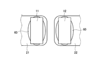
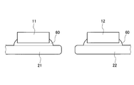
- the first semiconductor chip 11 is mounted on the chip mounting surface of the first lead frame 21.
- the control chip 111 and the transformer chip 112 are fixed to the first lead frame 21 by the die attach 60.
- the second semiconductor chip 12 is mounted on the chip mounting surface of the second lead frame 22.
- the second semiconductor chip 12 is fixed to the second lead frame 22 by the die attach 60.
- As the material of Diatouch 60 silver paste or the like is preferably used.
- the electric signal output from the control chip 111 is input to the transformer chip 112 via the connecting bonding wire 315. Then, the electric signal output from the transformer chip 112 is transmitted to the second semiconductor chip 12 via the connection bonding wire 30.
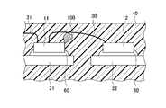
- the semiconductor device 1 shown in FIG. 1 is resin-sealed with a sealing resin 40.
- the sealing resin 40 is embedded between the first lead frame 21 and the second lead frame 22, and the first semiconductor chip 11, the second semiconductor chip 12, and the chips of the first lead frame 21 and the second lead frame 22 are embedded. It covers the circumference of the mounting surface. Further, the first bonding wire 311 that electrically connects the control chip 111 and the first lead frame 21 and the second bonding wire 321 that electrically connects the second semiconductor chip 12 and the second lead frame 22 are sealed. It is resin-sealed with a stop resin 40.
- the bonding wires (connecting bonding wires 315, first bonding wires 311 and the like) used for electrical connection with the first semiconductor chip 11 in the low voltage side region are referred to as "low voltage side bonding wires 31". Further, the bonding wires (connecting bonding wires 30, second bonding wires 321 and the like) used for electrical connection with the second semiconductor chip 12 in the high voltage side region are referred to as "high voltage side bonding wires 32".
- the proximity region A shown in FIG. 1 is a region in which the low voltage side region and the high voltage side region face each other and are close to each other.
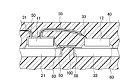
- the surfaces of the regions of the first lead frame 21 and the second lead frame 22 facing each other are covered with the insulating protective film 50 inside the sealing resin 40. That is, in the proximity region A, the surface of the region of the first lead frame 21 facing the second lead frame 22 and the surface of the region of the second lead frame 22 facing the first lead frame 21 are formed by the insulating protective film 50. It is covered. Further, in the proximity region A, the surfaces of the regions of the first semiconductor chip 11 and the first lead frame 21 and the connecting bonding wire 30 facing each other are covered with the insulating protective film 50. As described above, in the semiconductor device 1, the surface of the conductive member is covered with the insulating protective film 50 in the proximity region A.
- the insulating protective film 50 is made of a material having a higher dielectric breakdown voltage than the sealing resin 40.
- sealing resin 40 for example, an epoxy resin, a silicone resin, or the like can be adopted.
- insulating protective film 50 for example, a thermoplastic aromatic polyetheramideimide containing an aromatic hydrocarbon in its basic molecular structure can be adopted.
- the breakdown voltage of an epoxy resin generally used as a sealing resin for semiconductor devices is about 40 V / mm, whereas the breakdown voltage of thermoplastic aromatic polyetheramideimide is about 230 kV / mm. ..
- a resin in which a filler is mixed in the sealing resin 40 may be adopted, and a resin in which the filler is not mixed in the insulating protective film 50 or a resin having a lower filler content than the sealing resin 40 may be adopted. Accumulation of electric charge at the interface between the filler and the resin lowers the dielectric breakdown voltage of the resin containing the filler. Therefore, by adopting a resin having a filler content relatively lower than that of the sealing resin 40 for the insulating protective film 50, the insulating protective film 50 can be made of a material having a higher dielectric breakdown voltage than the sealing resin 40. it can.
- the insulating protective film 50 is preferably a soft material having a hardness lower than that of the sealing resin 40. Further, it is preferable to use a material having high adhesion to the sealing resin 40 for the insulating protective film 50.
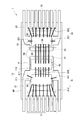
- FIG. 2 shows a plan view of the semiconductor device 1 according to the embodiment.
- one end is arranged inside the sealing resin 40, and the low voltage side lead terminal 71 and the high voltage side lead terminal 72 whose other end is exposed from the sealing resin 40 are provided.
- a plurality of low-voltage side lead terminals 71 are electrically connected to the control chip 111 via the first connection bonding wire 312, respectively.
- the plurality of high voltage side lead terminals 72 are electrically connected to the second semiconductor chip 12 via the second connection bonding wire 322.
- copper (Cu) is used as the material for the first lead frame 21, the second lead frame 22, the low voltage side lead terminal 71, and the high voltage side lead terminal 72.
- gold (Au) or aluminum (Al) is used as the material of the bonding wire.
- the sealing resin 40 is formed by molding or the like. At this time, foreign matter may be mixed inside the sealing resin 40.
- the conductive foreign matter 100 is mixed inside the sealing resin 40, and the first lead frame 21 in the low voltage side region and the second lead frame 22 in the high voltage side region are short-circuited by the foreign matter 100. Will be done. In that case, if a high power supply voltage is supplied to the second lead frame 22, the first semiconductor chip 11 mounted on the first lead frame 21 may undergo dielectric breakdown.
- the insulating protective film 50 made of a material having a higher dielectric breakdown voltage than the sealing resin 40 is formed on the first lead frame 21 and the second lead frame 22. It covers the surfaces of the respective regions facing each other. Therefore, even if the conductive foreign matter 100 straddles the first lead frame 21 and the second lead frame 22 and is mixed inside the sealing resin 40, the dielectric breakdown of the first semiconductor chip 11 is suppressed. ..
- the foreign matter 100 is mixed between the low-voltage side region and the high-voltage side region, so that the low-voltage side region and the high-voltage side are not completely short-circuited.
- the distance between the regions becomes narrow, and the first semiconductor chip 11 may undergo dielectric breakdown.
- the dielectric breakdown of the first semiconductor chip 11 is suppressed by covering the opposing surfaces of the low-voltage side region and the high-voltage side region with the insulating protective film 50.
- the foreign matter 100 adheres to the first lead frame 21 and the second lead frame 22, so that the first lead frame 21 and the second lead frame 22 are brought into close contact with the sealing resin 40.
- the sex is reduced.
- the insulating property also decreases.
- dielectric breakdown of the first semiconductor chip 11 is suppressed.
- the surface of the region of the first semiconductor chip 11 and the connecting bonding wire 30 facing each other is covered with the insulating protective film 50. Further, similarly to the first semiconductor chip 11, the surface of the die attach 60 is also covered with the insulating protective film 50 in the proximity region A. Therefore, it is possible to prevent the first semiconductor chip 11 and the connection bonding wire 30 from being short-circuited via the foreign matter 100. As a result, dielectric breakdown of the first semiconductor chip 11 is suppressed.
- the surface of the region facing each other between the connection bonding wire 30 and the other bonding wires connected to the first semiconductor chip 11 excluding the connection bonding wire 30 is covered with the insulating protective film 50.
- the region of the connecting bonding wire 315 close to the connecting bonding wire 30 and the region of the connecting bonding wire 30 close to the connecting bonding wire 315 are covered with the insulating protective film 50. Therefore, the short circuit between the connection bonding wire 30 and the low voltage side bonding wire 31 due to the mixing of the foreign matter 100 is prevented, and the dielectric breakdown of the first semiconductor chip 11 is suppressed.
- the bonding wires are bent in the process of forming the sealing resin 40 and the bonding wires come into contact with each other. According to the semiconductor device 1, it is possible to prevent a short circuit even when the connection bonding wire 30 and the low voltage side bonding wire 31 are deformed and come into contact with each other.
- the manufacturing method of the semiconductor device 1 shown in FIG. 1 will be described below.
- the semiconductor device manufacturing method described below is an example, and can be realized by various other manufacturing methods including this modification.
- a die-attaching step and a wire bonding step are carried out. That is, by the die attach step, the control chip 111 and the transformer chip 112 are fixed to the chip mounting surface of the first lead frame 21 by the die attach 60. Further, the second semiconductor chip 12 is fixed to the chip mounting surface of the second lead frame 22 by the die attach 60. Then, in the wire bonding step, the first lead frame 21 and the control chip 111 are connected by the first bonding wire 311 and the second lead frame 22 and the second semiconductor chip 12 are connected by the second bonding wire 321. Further, the control chip 111 and the transformer chip 112 are connected by the connecting bonding wire 315, and the transformer chip 112 and the second semiconductor chip 12 are connected by the connecting bonding wire 30.
- an insulating protective film 50 is formed on the surface of a predetermined member included in the proximity region A. That is, the surface of the region of the first lead frame 21 and the second lead frame 22 facing each other and the surface of the region of the first semiconductor chip 11 and the first lead frame 21 and the connecting bonding wire 30 facing each other are covered.
- the insulating protective film 50 is formed on the surface. For example, after dropping the liquid insulating protective film 50 onto the proximity region A, the insulating protective film 50 is cured.
- the sealing resin 40 is formed in a predetermined region of the semiconductor device 1 by molding. That is, by embedding between the first lead frame 21 and the second lead frame 22, the periphery of the chip mounting surfaces of the first semiconductor chip 11, the second semiconductor chip 12, and the first lead frame 21 and the second lead frame 22.
- the sealing resin 40 is formed so as to cover the above. As a result, the semiconductor device 1 shown in FIG. 1 is completed.
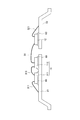
- the corner portion formed by the facing side surfaces of the first lead frame 21 and the second lead frame 22 facing each other and the other side surfaces connected to the facing side surfaces is the chip mounting surface. It is preferable that the surface is chamfered when viewed from the normal direction. By making the corners of the first lead frame 21 and the second lead frame 22 curved, the concentration of the electric field at the corners is relaxed. As a result, the withstand voltage of the semiconductor device can be improved.
- the corners of the first lead frame 21 and the second lead frame 22 may be C-chamfered.
- the corner portion formed by the facing side surfaces of the first lead frame 21 and the second lead frame 22 facing each other and the main surface connected to the facing side surfaces is R-chamfered.
- the corner portion formed by the upper surface on which the semiconductor chip is mounted and the facing side surface is R-chamfered, and the corner portion formed by the lower surface facing the upper surface and the facing side surface is R-chamfered.
- FIG. 12 shows an example of a circuit using the semiconductor device 1 according to the embodiment.
- the first transistor T1 and the second transistor T2 are longitudinally connected between the power supply voltage Vgt and the ground potential.
- the power supply voltage Vgt connected to the first transistor T1 is 600V to 1000V.
- the potential Vout of the output terminal, which is the connection point between the first transistor T1 and the second transistor T2, is set by the on / off state of the first transistor T1 and the second transistor T2.
- the first transistor T1 and the second transistor T2 are, for example, IGBTs and MOSFETs.
- the operation of the second transistor T2 is controlled by the semiconductor device 2.
- the second reference potential Vs2 of the semiconductor device 2 is the ground potential, and the second power supply voltage Vg2 is supplied to the semiconductor device 2.
- the potential of the second power supply voltage Vg2 is about 5V to 20V.
- the semiconductor device 1 controls the operation of the first transistor T1.
- the first reference potential Vs1 is set to the potential Vout of the output terminal, and the first power supply voltage Vg1 is supplied.
- the potential difference between the first reference potential Vs1 and the first power supply voltage Vg1 is, for example, about 5V to 20V.
- the first reference potential Vs1 is low when the second transistor T2 is on and the first transistor T1 is off.
- the first reference potential Vs1 when the first transistor T1 is on and the second transistor T2 is off is a high potential of about 600V to 1000V depending on the power supply voltage Vgt.
- the power supply voltage supplied to the second semiconductor chip 12 that drives the first transistor T1 is high.
- the semiconductor device 1 drives, for example, the first transistor T1 connected to a power supply voltage Vgt of 1000 V.
- Vgt a power supply voltage
- the electric signal is transmitted between the first semiconductor chip 11 and the second semiconductor chip 12 via the transformer chip 112 that converts the electric signal and the magnetic force. Therefore, dielectric breakdown of the first semiconductor chip 11 can be suppressed.
- An inductor-coupled insulating element that transmits an electric signal in an insulated state by inductively coupling a pair of inductors (coils) composed of a receiving-side inductor and a transmitting-side inductor is preferably used for the transformer chip 112.
- the receiving side inductor converts an electric signal into a magnetic force
- the transmitting side inductor converts this magnetic force into an electric signal.
- FIG. 13 shows a configuration example of the transformer chip 112.
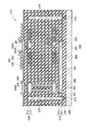
- the transformer chip 112 has a configuration in which a plurality of insulating layers 210 are laminated on the semiconductor substrate 200.
- the semiconductor substrate 200 is, for example, a silicon substrate or a silicon carbide substrate.
- FIG. 13 shows an example in which 12 insulating layers 210 are laminated on the semiconductor substrate 200.
- the number of layers of the insulating layer 210 is not limited to 12.
- the number of layers of the insulating layer 210 is set according to the withstand voltage required for the transformer chip 112 and the like.
- Each of the insulating layers 210 has a structure in which the etching stopper film 211 and the interlayer film 212 are laminated with the etching stopper film 211 as the lower layer and the interlayer film 212 as the upper layer.
- the etching stopper film 211 is, for example, a silicon nitride (SiN) film or a silicon carbide (SiC) film.
- the interlayer film 212 is, for example, a silicon dioxide (SiO 2 ) film.
- the insulating layer 210 of the lowermost layer does not have the etching stopper film 211, and the interlayer film 212 is directly arranged on the main surface of the semiconductor substrate 200.
- the etching stopper film 211 made of a SiN film has a tensile stress.
- the interlayer film 212 made of a SiO 2 film has a compressive stress. Further, the etching stopper film 211 prevents Cu contained in the Cu wiring material described later from diffusing into the interlayer film 212.
- a coil 220 in which an upper coil 221 and a lower coil 222 are paired is arranged inside the transformer chip 112.
- the upper coil 221 and the lower coil 222 face each other via a plurality of layers of insulating layers 210.
- the upper coil 221 and the lower coil 222 are made of a conductor and are formed in an elliptical spiral shape in a plan view.
- the upper coil inner wiring 221A connected to the inner end of the upper coil 221 is arranged at the center of the upper coil 221.
- the lower coil inner wiring 222A connected to the inner end of the lower coil 222 is arranged at the center of the lower coil 222.
- the lower coil outer wiring 222B connected to the outer end of the lower coil 222 is arranged.
- the upper coil 221 and the lower coil 222 penetrate one layer of the insulating layer 210 in the film thickness direction.
- the lower coil 222 is arranged on the insulating layer 210 of the fourth layer counting from the semiconductor substrate 200 side, and the upper coil 221 is arranged on the insulating layer 210 of the eleventh layer.
- a Cu wiring material containing Cu as a main component is used for the upper coil 221 and the lower coil 222.
- a laminated film of tantalum (Ta) / tantalum nitride (TaN) / tantalum (Ta) may be formed as a barrier metal layer on the side surfaces of the upper coil 221 and the lower coil 222.
- the barrier metal layer prevents Cu contained in the Cu wiring material from diffusing into the interlayer film 212.
- the low voltage electrode layer 241 is arranged in the insulating layer 210 below the insulating layer 210 in which the lower coil 222 is arranged.
- the lower coil inner wiring 222A and the low voltage electrode layer 241 are electrically connected by a columnar first low voltage wiring 251 penetrating the insulating layer 210 located in the middle.
- the low voltage electrode layer 241 is electrically connected to the semiconductor substrate 200 via the ground wiring 260.
- the lower low voltage wiring 242 is arranged in the insulating layer 210 in which the lower coil 222 is arranged.
- the low-voltage electrode layer 241 and the lower low-voltage wiring 242 are electrically connected by a columnar second low-voltage wiring 252 penetrating the insulating layer 210 located in the middle.
- the upper low voltage wiring 243 is arranged in the insulating layer 210 in which the upper coil 221 is arranged.
- the lower low-voltage wiring 242 and the upper low-voltage wiring 243 are electrically connected by a columnar third low-voltage wiring 253 penetrating the insulating layer 210 located in the middle.
- a protective insulating film 290 is arranged on the upper surface of the transformer chip 112.
- the protective insulating film 290 has a laminated structure in which the coil protective film 292 is arranged on the upper surface of the passivation film 291.
- the low voltage electrode 240A and the high voltage electrode 250A are arranged apart from each other on the surface of the uppermost insulating layer 210 exposed to the opening provided in the protective insulating film 290.
- aluminum (Al) is used as the material for the low voltage electrode 240A and the high voltage electrode 250A.
- the passivation film 291 has, for example, a laminated structure of a silicon dioxide film / silicon nitride film.
- the coil protective film 292 is, for example, a polyimide film.
- the coil protective film 292 is arranged above the coil 220, and the coil 220 is covered with the coil protective film 292 in a plan view.
- the low-voltage electrode 240A is electrically connected to the upper low-voltage wiring 243 arranged below by the columnar fourth low-voltage wiring 254 penetrating the insulating layer 210 located in the middle. That is, the low-voltage electrode 240A is connected to the lower coil inner wiring 222A via the upper low-voltage wiring 243, the lower low-voltage wiring 242, the low-voltage electrode layer 241 and the first low-voltage wiring 251 to the fourth low-voltage wiring 254. It is electrically connected.
- the high-voltage electrode 250A is electrically connected to the upper coil inner wiring 221A arranged below by a columnar high-voltage wiring 261 penetrating the insulating layer 210 located in the middle.
- the shield layer 270 is arranged so as to surround the coil 220 and the wiring connecting the coil 220 with the low voltage electrode 240A and the high voltage electrode 250A.
- the lower end of the shield layer 270 and the semiconductor substrate 200 are electrically connected by the shield ground wiring 275.
- the wiring and the shield layer 270 arranged inside the transformer chip 112 use a laminated structure of Cu and a barrier metal layer like the coil 220, for example.
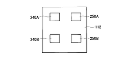
- FIG. 16 is a plan view showing an arrangement example of the electrodes of the transformer chip 112.
- the low-voltage electrode 240B shown in FIG. 16 is connected to the lower coil inner wiring 222A and the low-voltage electrode 240A via a wiring arranged inside the transformer chip 112. Electrically connect to the coil.
- the high voltage electrode 250B is electrically connected to the upper coil via the wiring arranged inside the transformer chip 112 in the same manner as connecting the upper coil inner wiring 221A and the high voltage electrode 250A. Connect to.
- the electric signal output from the control chip 111 is input to the low voltage electrode 240A and the low voltage electrode 240B of the transformer chip 112.
- This electric signal is converted into a magnetic force by the lower coil 222 formed inside the transformer chip 112.
- This magnetic force is converted into an electric signal by the upper coil 221 arranged to face the lower coil 222.
- the converted electric signal is output to the second semiconductor chip 12 via the high voltage electrode 250A and the high voltage electrode 250B of the transformer chip 112.
- the lower coil 222 functions as the receiving side inductor and the upper coil 221 functions as the transmitting side inductor. Therefore, the electric signal does not directly propagate between the control chip 111 and the second semiconductor chip 12. As a result, it is possible to prevent the control chip 111 from undergoing dielectric breakdown due to the high voltage supplied to the second semiconductor chip 12.
Landscapes
- Semiconductor Integrated Circuits (AREA)
- Structures Or Materials For Encapsulating Or Coating Semiconductor Devices Or Solid State Devices (AREA)
- Lead Frames For Integrated Circuits (AREA)
Abstract
Description
Claims (9)
- 第1の電源電圧が供給される第1半導体チップと、
前記第1の電源電圧よりも電位が高い第2の電源電圧が供給される第2半導体チップと、
前記第1半導体チップが搭載されるチップ搭載面を有する第1リードフレームと、
前記第2半導体チップが搭載されるチップ搭載面を有する第2リードフレームと、
前記第1半導体チップと前記第2半導体チップを電気的に接続する接続ボンディングワイヤと、
前記第1リードフレームと前記第2リードフレームの間を埋め込んで、前記第1半導体チップ、前記第2半導体チップ、及び、前記第1リードフレームと前記第2リードフレームそれぞれの前記チップ搭載面の周囲を覆って配置された封止樹脂と、
前記封止樹脂よりも絶縁破壊電圧が高い材料からなり、前記第1リードフレームと前記第2リードフレームの相互に対向する領域の表面を前記封止樹脂の内部で覆う絶縁保護膜と
を備える、半導体装置。 - 前記絶縁保護膜が、前記封止樹脂の内部で前記第1半導体チップ及び前記第1リードフレームと前記接続ボンディングワイヤの相互に対向する領域の表面を更に覆う、請求項1に記載の半導体装置。
- 前記絶縁保護膜が、前記接続ボンディングワイヤを除いた前記第1半導体チップに接続するボンディングワイヤの前記接続ボンディングワイヤと対向する領域を覆う、請求項1又は2に記載の半導体装置。
- 前記絶縁保護膜の材料が、前記封止樹脂の材料の樹脂よりもフィラーの含有率が相対的に低い樹脂である、請求項1乃至3のいずれか1項に記載の半導体装置。
- 前記絶縁保護膜が、前記封止樹脂よりも硬度が低い材料である、請求項1乃至4のいずれか1項に記載の半導体装置。
- 前記第1リードフレームと前記第2リードフレームが相互に対向するそれぞれの対向側面と、前記対向側面と連結する他の側面とがなすコーナー部が、R面取りされている、請求項1乃至5のいずれか1項に記載の半導体装置。
- 前記第1リードフレームと前記第2リードフレームが相互に対向するそれぞれの対向側面と、前記対向側面に連結する主面とがなすコーナー部が、R面取りされている、請求項1乃至5のいずれか1項に記載の半導体装置。
- 制御チップ、及び前記制御チップが出力する電気信号を内部で磁力に変換した後に前記磁力を電気信号に変換して出力するトランスチップを前記第1半導体チップとして有し、
前記トランスチップの出力する電気信号が入力する前記第2半導体チップが、前記制御チップに制御されてスイッチング素子を駆動する駆動チップとして動作する、
請求項1乃至7のいずれか1項に記載の半導体装置。 - 前記制御チップと前記駆動チップに挟まれた位置に前記トランスチップが配置され、
前記トランスチップの前記駆動チップと対向する表面、及び、前記トランスチップと前記駆動チップを電気的に接続する前記接続ボンディングワイヤの表面が、前記絶縁保護膜に覆われている、請求項8に記載の半導体装置。
Priority Applications (4)
| Application Number | Priority Date | Filing Date | Title |
|---|---|---|---|
| JP2021525939A JP7496821B2 (ja) | 2019-06-11 | 2020-04-28 | 半導体装置 |
| DE112020002828.3T DE112020002828T5 (de) | 2019-06-11 | 2020-04-28 | Halbleiterbauteil |
| CN202080042917.1A CN114026683B (zh) | 2019-06-11 | 2020-04-28 | 半导体器件 |
| US17/454,576 US12136589B2 (en) | 2019-06-11 | 2021-11-11 | Semiconductor device |
Applications Claiming Priority (2)
| Application Number | Priority Date | Filing Date | Title |
|---|---|---|---|
| JP2019-108677 | 2019-06-11 | ||
| JP2019108677 | 2019-06-11 |
Related Child Applications (1)
| Application Number | Title | Priority Date | Filing Date |
|---|---|---|---|
| US17/454,576 Continuation US12136589B2 (en) | 2019-06-11 | 2021-11-11 | Semiconductor device |
Publications (1)
| Publication Number | Publication Date |
|---|---|
| WO2020250592A1 true WO2020250592A1 (ja) | 2020-12-17 |
Family
ID=73781761
Family Applications (1)
| Application Number | Title | Priority Date | Filing Date |
|---|---|---|---|
| PCT/JP2020/018144 Ceased WO2020250592A1 (ja) | 2019-06-11 | 2020-04-28 | 半導体装置 |
Country Status (5)
| Country | Link |
|---|---|
| US (1) | US12136589B2 (ja) |
| JP (1) | JP7496821B2 (ja) |
| CN (1) | CN114026683B (ja) |
| DE (1) | DE112020002828T5 (ja) |
| WO (1) | WO2020250592A1 (ja) |
Cited By (1)
| Publication number | Priority date | Publication date | Assignee | Title |
|---|---|---|---|---|
| WO2022130906A1 (ja) * | 2020-12-18 | 2022-06-23 | ローム株式会社 | 半導体装置 |
Citations (5)
| Publication number | Priority date | Publication date | Assignee | Title |
|---|---|---|---|---|
| JPH06112370A (ja) * | 1992-09-29 | 1994-04-22 | Nec Corp | 半導体装置 |
| JP2005005638A (ja) * | 2003-04-15 | 2005-01-06 | Fuji Electric Fa Components & Systems Co Ltd | 半導体モジュールおよびその製造方法 |
| JP2015050222A (ja) * | 2013-08-30 | 2015-03-16 | 株式会社デンソー | 半導体装置 |
| JP2016207714A (ja) * | 2015-04-16 | 2016-12-08 | ローム株式会社 | 半導体装置 |
| JP2017183695A (ja) * | 2016-03-24 | 2017-10-05 | 富士電機株式会社 | 半導体装置 |
Family Cites Families (11)
| Publication number | Priority date | Publication date | Assignee | Title |
|---|---|---|---|---|
| JPH0567708A (ja) * | 1991-09-09 | 1993-03-19 | Seiko Epson Corp | 半導体集積回路のパツケージ方法 |
| JPH0745755A (ja) * | 1991-11-27 | 1995-02-14 | Ricoh Co Ltd | 樹脂封止型半導体装置とその製造方法 |
| JPH06275767A (ja) * | 1993-03-22 | 1994-09-30 | Toshiba Corp | 樹脂封止型半導体装置の製造方法 |
| JP2006060065A (ja) * | 2004-08-20 | 2006-03-02 | Mitsubishi Electric Corp | 半導体装置および半導体装置の製造方法 |
| KR20060109092A (ko) * | 2005-04-15 | 2006-10-19 | 주식회사 하이닉스반도체 | 반도체 소자의 멀티 칩 패키지 방법 |
| JP5096278B2 (ja) | 2008-09-26 | 2012-12-12 | ローム株式会社 | 半導体装置及び半導体装置の製造方法 |
| US20120153444A1 (en) * | 2009-06-18 | 2012-06-21 | Rohm Co., Ltd | Semiconductor device |
| JP2012174996A (ja) * | 2011-02-23 | 2012-09-10 | Fujitsu Ltd | 半導体装置及び半導体装置の製造方法 |
| CN102543937B (zh) * | 2011-12-30 | 2014-01-22 | 北京工业大学 | 一种芯片上倒装芯片封装及制造方法 |
| JP6271221B2 (ja) * | 2013-11-08 | 2018-01-31 | ルネサスエレクトロニクス株式会社 | 半導体装置 |
| US10256169B2 (en) | 2016-03-24 | 2019-04-09 | Fuji Electric Co., Ltd. | Semiconductor device |
-
2020
- 2020-04-28 JP JP2021525939A patent/JP7496821B2/ja active Active
- 2020-04-28 WO PCT/JP2020/018144 patent/WO2020250592A1/ja not_active Ceased
- 2020-04-28 DE DE112020002828.3T patent/DE112020002828T5/de active Pending
- 2020-04-28 CN CN202080042917.1A patent/CN114026683B/zh active Active
-
2021
- 2021-11-11 US US17/454,576 patent/US12136589B2/en active Active
Patent Citations (5)
| Publication number | Priority date | Publication date | Assignee | Title |
|---|---|---|---|---|
| JPH06112370A (ja) * | 1992-09-29 | 1994-04-22 | Nec Corp | 半導体装置 |
| JP2005005638A (ja) * | 2003-04-15 | 2005-01-06 | Fuji Electric Fa Components & Systems Co Ltd | 半導体モジュールおよびその製造方法 |
| JP2015050222A (ja) * | 2013-08-30 | 2015-03-16 | 株式会社デンソー | 半導体装置 |
| JP2016207714A (ja) * | 2015-04-16 | 2016-12-08 | ローム株式会社 | 半導体装置 |
| JP2017183695A (ja) * | 2016-03-24 | 2017-10-05 | 富士電機株式会社 | 半導体装置 |
Cited By (2)
| Publication number | Priority date | Publication date | Assignee | Title |
|---|---|---|---|---|
| WO2022130906A1 (ja) * | 2020-12-18 | 2022-06-23 | ローム株式会社 | 半導体装置 |
| JPWO2022130906A1 (ja) * | 2020-12-18 | 2022-06-23 |
Also Published As
| Publication number | Publication date |
|---|---|
| JPWO2020250592A1 (ja) | 2020-12-17 |
| DE112020002828T5 (de) | 2022-02-24 |
| US20220068776A1 (en) | 2022-03-03 |
| CN114026683B (zh) | 2025-11-04 |
| JP7496821B2 (ja) | 2024-06-07 |
| US12136589B2 (en) | 2024-11-05 |
| CN114026683A (zh) | 2022-02-08 |
Similar Documents
| Publication | Publication Date | Title |
|---|---|---|
| US12401000B2 (en) | Semiconductor device | |
| US12002785B2 (en) | Semiconductor device | |
| US9368434B2 (en) | Electronic component | |
| US10147707B2 (en) | Semiconductor device | |
| CN203859110U (zh) | 双标记板堆叠式管芯封装件与半导体封装件 | |
| US8546926B2 (en) | Power converter | |
| US20220208674A1 (en) | Insulating chip | |
| US10720411B2 (en) | Semiconductor device | |
| WO2016157394A1 (ja) | 半導体装置およびその製造方法 | |
| KR20200011893A (ko) | 대칭적으로 배열된 전원 단자를 갖는 반도체 패키지 및 그 제조 방법 | |
| US20240186310A1 (en) | Signal transmission device and insulation chip | |
| US20240029949A1 (en) | Insulating transformer | |
| CN120981920A (zh) | 具有背面变压器的电压隔离集成电路封装件 | |
| CN114026683B (zh) | 半导体器件 | |
| JP2026032228A (ja) | 半導体装置および半導体モジュール | |
| US20250014799A1 (en) | Insulating chip and signal transmission device | |
| US20240313043A1 (en) | Insulation chip and signal transmission device | |
| CN118339651A (zh) | 半导体装置 | |
| US20240332171A1 (en) | Insulation chip and signal transmission device | |
| US20250070103A1 (en) | Semiconductor device | |
| US20240186309A1 (en) | Signal transmitting device and insulating chip | |
| US20260114337A1 (en) | Semiconductor device and insulating switch | |
| US20250072012A1 (en) | Semiconductor device | |
| US20250309178A1 (en) | Semiconductor device | |
| JP2024173373A (ja) | 信号伝達装置 |
Legal Events
| Date | Code | Title | Description |
|---|---|---|---|
| 121 | Ep: the epo has been informed by wipo that ep was designated in this application |
Ref document number: 20822507 Country of ref document: EP Kind code of ref document: A1 |
|
| ENP | Entry into the national phase |
Ref document number: 2021525939 Country of ref document: JP Kind code of ref document: A |
|
| 122 | Ep: pct application non-entry in european phase |
Ref document number: 20822507 Country of ref document: EP Kind code of ref document: A1 |
|
| WWG | Wipo information: grant in national office |
Ref document number: 202080042917.1 Country of ref document: CN |