WO2020250083A1 - 半導体装置、および半導体装置の作製方法 - Google Patents
半導体装置、および半導体装置の作製方法 Download PDFInfo
- Publication number
- WO2020250083A1 WO2020250083A1 PCT/IB2020/055190 IB2020055190W WO2020250083A1 WO 2020250083 A1 WO2020250083 A1 WO 2020250083A1 IB 2020055190 W IB2020055190 W IB 2020055190W WO 2020250083 A1 WO2020250083 A1 WO 2020250083A1
- Authority
- WO
- WIPO (PCT)
- Prior art keywords
- insulator
- oxide
- film
- conductor
- semiconductor
- Prior art date
Links
- 239000004065 semiconductor Substances 0.000 title claims abstract description 438
- 238000004519 manufacturing process Methods 0.000 title claims description 68
- 229910052760 oxygen Inorganic materials 0.000 claims description 261
- 239000001301 oxygen Substances 0.000 claims description 259
- QVGXLLKOCUKJST-UHFFFAOYSA-N atomic oxygen Chemical compound [O] QVGXLLKOCUKJST-UHFFFAOYSA-N 0.000 claims description 251
- 238000000034 method Methods 0.000 claims description 236
- 238000010438 heat treatment Methods 0.000 claims description 134
- 238000004544 sputter deposition Methods 0.000 claims description 100
- 229910044991 metal oxide Inorganic materials 0.000 claims description 96
- 150000004706 metal oxides Chemical class 0.000 claims description 93
- IJGRMHOSHXDMSA-UHFFFAOYSA-N Atomic nitrogen Chemical compound N#N IJGRMHOSHXDMSA-UHFFFAOYSA-N 0.000 claims description 85
- 239000012298 atmosphere Substances 0.000 claims description 66
- 238000000231 atomic layer deposition Methods 0.000 claims description 63
- 238000012545 processing Methods 0.000 claims description 53
- 238000005229 chemical vapour deposition Methods 0.000 claims description 49
- 229910052710 silicon Inorganic materials 0.000 claims description 49
- 239000010703 silicon Substances 0.000 claims description 49
- 229910052782 aluminium Inorganic materials 0.000 claims description 48
- XAGFODPZIPBFFR-UHFFFAOYSA-N aluminium Chemical compound [Al] XAGFODPZIPBFFR-UHFFFAOYSA-N 0.000 claims description 48
- 229910052757 nitrogen Inorganic materials 0.000 claims description 36
- 229910000449 hafnium oxide Inorganic materials 0.000 claims description 28
- WIHZLLGSGQNAGK-UHFFFAOYSA-N hafnium(4+);oxygen(2-) Chemical compound [O-2].[O-2].[Hf+4] WIHZLLGSGQNAGK-UHFFFAOYSA-N 0.000 claims description 28
- 229910052715 tantalum Inorganic materials 0.000 claims description 23
- GUVRBAGPIYLISA-UHFFFAOYSA-N tantalum atom Chemical compound [Ta] GUVRBAGPIYLISA-UHFFFAOYSA-N 0.000 claims description 23
- 229910052738 indium Inorganic materials 0.000 claims description 21
- 229910052733 gallium Inorganic materials 0.000 claims description 20
- 229910052725 zinc Inorganic materials 0.000 claims description 11
- 239000012299 nitrogen atmosphere Substances 0.000 claims description 8
- 230000001681 protective effect Effects 0.000 claims description 4
- 230000001678 irradiating effect Effects 0.000 claims description 3
- 239000012212 insulator Substances 0.000 description 1119
- 239000004020 conductor Substances 0.000 description 546
- 239000010408 film Substances 0.000 description 491
- 230000006870 function Effects 0.000 description 220
- 239000010410 layer Substances 0.000 description 218
- 229910052739 hydrogen Inorganic materials 0.000 description 180
- 239000001257 hydrogen Substances 0.000 description 180
- UFHFLCQGNIYNRP-UHFFFAOYSA-N Hydrogen Chemical compound [H][H] UFHFLCQGNIYNRP-UHFFFAOYSA-N 0.000 description 166
- 239000000758 substrate Substances 0.000 description 161
- 239000012535 impurity Substances 0.000 description 105
- 230000015654 memory Effects 0.000 description 100
- 239000000463 material Substances 0.000 description 97
- 229910052581 Si3N4 Inorganic materials 0.000 description 93
- HQVNEWCFYHHQES-UHFFFAOYSA-N silicon nitride Chemical compound N12[Si]34N5[Si]62N3[Si]51N64 HQVNEWCFYHHQES-UHFFFAOYSA-N 0.000 description 91
- 239000007789 gas Substances 0.000 description 90
- 210000004027 cell Anatomy 0.000 description 89
- 230000002829 reductive effect Effects 0.000 description 89
- 230000015572 biosynthetic process Effects 0.000 description 76
- VYPSYNLAJGMNEJ-UHFFFAOYSA-N Silicium dioxide Chemical compound O=[Si]=O VYPSYNLAJGMNEJ-UHFFFAOYSA-N 0.000 description 75
- 238000003860 storage Methods 0.000 description 70
- 229910052814 silicon oxide Inorganic materials 0.000 description 66
- XLYOFNOQVPJJNP-UHFFFAOYSA-N water Substances O XLYOFNOQVPJJNP-UHFFFAOYSA-N 0.000 description 65
- 229910001868 water Inorganic materials 0.000 description 65
- 239000013078 crystal Substances 0.000 description 58
- 229910052751 metal Inorganic materials 0.000 description 57
- XUIMIQQOPSSXEZ-UHFFFAOYSA-N Silicon Chemical compound [Si] XUIMIQQOPSSXEZ-UHFFFAOYSA-N 0.000 description 48
- 239000002184 metal Substances 0.000 description 48
- 239000011701 zinc Substances 0.000 description 48
- 238000009792 diffusion process Methods 0.000 description 47
- 210000002381 plasma Anatomy 0.000 description 46
- 229910052735 hafnium Inorganic materials 0.000 description 42
- 150000004767 nitrides Chemical class 0.000 description 41
- TWNQGVIAIRXVLR-UHFFFAOYSA-N oxo(oxoalumanyloxy)alumane Chemical compound O=[Al]O[Al]=O TWNQGVIAIRXVLR-UHFFFAOYSA-N 0.000 description 38
- VBJZVLUMGGDVMO-UHFFFAOYSA-N hafnium atom Chemical compound [Hf] VBJZVLUMGGDVMO-UHFFFAOYSA-N 0.000 description 37
- 239000000203 mixture Substances 0.000 description 30
- 125000004429 atom Chemical group 0.000 description 29
- PXHVJJICTQNCMI-UHFFFAOYSA-N Nickel Chemical group [Ni] PXHVJJICTQNCMI-UHFFFAOYSA-N 0.000 description 28
- 230000004888 barrier function Effects 0.000 description 28
- 238000010586 diagram Methods 0.000 description 27
- 238000004549 pulsed laser deposition Methods 0.000 description 27
- 206010021143 Hypoxia Diseases 0.000 description 26
- -1 for example Chemical compound 0.000 description 26
- OKTJSMMVPCPJKN-UHFFFAOYSA-N Carbon Chemical compound [C] OKTJSMMVPCPJKN-UHFFFAOYSA-N 0.000 description 25
- 238000001451 molecular beam epitaxy Methods 0.000 description 25
- 239000000523 sample Substances 0.000 description 25
- 230000007547 defect Effects 0.000 description 24
- 229910052799 carbon Inorganic materials 0.000 description 23
- 229910052721 tungsten Inorganic materials 0.000 description 22
- 239000010937 tungsten Substances 0.000 description 22
- RTAQQCXQSZGOHL-UHFFFAOYSA-N Titanium Chemical group [Ti] RTAQQCXQSZGOHL-UHFFFAOYSA-N 0.000 description 21
- 229910052719 titanium Inorganic materials 0.000 description 21
- 239000010936 titanium Chemical group 0.000 description 21
- WFKWXMTUELFFGS-UHFFFAOYSA-N tungsten Chemical compound [W] WFKWXMTUELFFGS-UHFFFAOYSA-N 0.000 description 21
- 238000004140 cleaning Methods 0.000 description 20
- 238000001312 dry etching Methods 0.000 description 19
- RYGMFSIKBFXOCR-UHFFFAOYSA-N Copper Chemical group [Cu] RYGMFSIKBFXOCR-UHFFFAOYSA-N 0.000 description 18
- 238000005530 etching Methods 0.000 description 18
- 239000002356 single layer Substances 0.000 description 18
- MYMOFIZGZYHOMD-UHFFFAOYSA-N Dioxygen Chemical compound O=O MYMOFIZGZYHOMD-UHFFFAOYSA-N 0.000 description 17
- 238000007789 sealing Methods 0.000 description 17
- 239000011261 inert gas Substances 0.000 description 16
- 238000013473 artificial intelligence Methods 0.000 description 15
- 229910052802 copper Inorganic materials 0.000 description 15
- 239000010949 copper Chemical group 0.000 description 15
- 230000007423 decrease Effects 0.000 description 15
- 150000002431 hydrogen Chemical class 0.000 description 15
- APFVFJFRJDLVQX-UHFFFAOYSA-N indium atom Chemical compound [In] APFVFJFRJDLVQX-UHFFFAOYSA-N 0.000 description 15
- GYHNNYVSQQEPJS-UHFFFAOYSA-N Gallium Chemical group [Ga] GYHNNYVSQQEPJS-UHFFFAOYSA-N 0.000 description 14
- 229910001873 dinitrogen Inorganic materials 0.000 description 14
- 229910052759 nickel Inorganic materials 0.000 description 14
- 230000008569 process Effects 0.000 description 14
- KRHYYFGTRYWZRS-UHFFFAOYSA-N Fluorane Chemical compound F KRHYYFGTRYWZRS-UHFFFAOYSA-N 0.000 description 13
- NRTOMJZYCJJWKI-UHFFFAOYSA-N Titanium nitride Chemical compound [Ti]#N NRTOMJZYCJJWKI-UHFFFAOYSA-N 0.000 description 13
- 229910001882 dioxygen Inorganic materials 0.000 description 13
- 239000011229 interlayer Substances 0.000 description 13
- XEEYBQQBJWHFJM-UHFFFAOYSA-N Iron Chemical group [Fe] XEEYBQQBJWHFJM-UHFFFAOYSA-N 0.000 description 12
- 238000004364 calculation method Methods 0.000 description 12
- 230000004048 modification Effects 0.000 description 12
- 238000012986 modification Methods 0.000 description 12
- 230000003647 oxidation Effects 0.000 description 12
- 238000007254 oxidation reaction Methods 0.000 description 12
- RVTZCBVAJQQJTK-UHFFFAOYSA-N oxygen(2-);zirconium(4+) Chemical compound [O-2].[O-2].[Zr+4] RVTZCBVAJQQJTK-UHFFFAOYSA-N 0.000 description 12
- 239000010453 quartz Substances 0.000 description 12
- 229910001928 zirconium oxide Inorganic materials 0.000 description 12
- XKRFYHLGVUSROY-UHFFFAOYSA-N Argon Chemical compound [Ar] XKRFYHLGVUSROY-UHFFFAOYSA-N 0.000 description 11
- ZOKXTWBITQBERF-UHFFFAOYSA-N Molybdenum Chemical compound [Mo] ZOKXTWBITQBERF-UHFFFAOYSA-N 0.000 description 11
- 229910052750 molybdenum Inorganic materials 0.000 description 11
- 239000011733 molybdenum Substances 0.000 description 11
- 239000011347 resin Substances 0.000 description 11
- 229920005989 resin Polymers 0.000 description 11
- 229910052707 ruthenium Inorganic materials 0.000 description 11
- 239000000126 substance Substances 0.000 description 11
- YCKRFDGAMUMZLT-UHFFFAOYSA-N Fluorine atom Chemical compound [F] YCKRFDGAMUMZLT-UHFFFAOYSA-N 0.000 description 10
- AJNVQOSZGJRYEI-UHFFFAOYSA-N digallium;oxygen(2-) Chemical compound [O-2].[O-2].[O-2].[Ga+3].[Ga+3] AJNVQOSZGJRYEI-UHFFFAOYSA-N 0.000 description 10
- 230000000694 effects Effects 0.000 description 10
- 229910052731 fluorine Inorganic materials 0.000 description 10
- 239000011737 fluorine Substances 0.000 description 10
- 229910001195 gallium oxide Inorganic materials 0.000 description 10
- MZLGASXMSKOWSE-UHFFFAOYSA-N tantalum nitride Chemical compound [Ta]#N MZLGASXMSKOWSE-UHFFFAOYSA-N 0.000 description 10
- 238000012546 transfer Methods 0.000 description 10
- FYYHWMGAXLPEAU-UHFFFAOYSA-N Magnesium Chemical compound [Mg] FYYHWMGAXLPEAU-UHFFFAOYSA-N 0.000 description 9
- QCWXUUIWCKQGHC-UHFFFAOYSA-N Zirconium Chemical compound [Zr] QCWXUUIWCKQGHC-UHFFFAOYSA-N 0.000 description 9
- 238000006243 chemical reaction Methods 0.000 description 9
- 230000005684 electric field Effects 0.000 description 9
- 229910052749 magnesium Inorganic materials 0.000 description 9
- 239000011777 magnesium Substances 0.000 description 9
- 238000002156 mixing Methods 0.000 description 9
- 230000001590 oxidative effect Effects 0.000 description 9
- 230000002093 peripheral effect Effects 0.000 description 9
- 229910052727 yttrium Inorganic materials 0.000 description 9
- VWQVUPCCIRVNHF-UHFFFAOYSA-N yttrium atom Chemical group [Y] VWQVUPCCIRVNHF-UHFFFAOYSA-N 0.000 description 9
- 229910052726 zirconium Inorganic materials 0.000 description 9
- MWUXSHHQAYIFBG-UHFFFAOYSA-N Nitric oxide Chemical compound O=[N] MWUXSHHQAYIFBG-UHFFFAOYSA-N 0.000 description 8
- KJTLSVCANCCWHF-UHFFFAOYSA-N Ruthenium Chemical compound [Ru] KJTLSVCANCCWHF-UHFFFAOYSA-N 0.000 description 8
- XLOMVQKBTHCTTD-UHFFFAOYSA-N Zinc monoxide Chemical compound [Zn]=O XLOMVQKBTHCTTD-UHFFFAOYSA-N 0.000 description 8
- 230000000875 corresponding effect Effects 0.000 description 8
- 238000010894 electron beam technology Methods 0.000 description 8
- 229910052732 germanium Inorganic materials 0.000 description 8
- GNPVGFCGXDBREM-UHFFFAOYSA-N germanium atom Chemical group [Ge] GNPVGFCGXDBREM-UHFFFAOYSA-N 0.000 description 8
- 229910003437 indium oxide Inorganic materials 0.000 description 8
- PJXISJQVUVHSOJ-UHFFFAOYSA-N indium(iii) oxide Chemical compound [O-2].[O-2].[O-2].[In+3].[In+3] PJXISJQVUVHSOJ-UHFFFAOYSA-N 0.000 description 8
- 230000010354 integration Effects 0.000 description 8
- 229910052746 lanthanum Inorganic materials 0.000 description 8
- FZLIPJUXYLNCLC-UHFFFAOYSA-N lanthanum atom Chemical compound [La] FZLIPJUXYLNCLC-UHFFFAOYSA-N 0.000 description 8
- CPLXHLVBOLITMK-UHFFFAOYSA-N magnesium oxide Inorganic materials [Mg]=O CPLXHLVBOLITMK-UHFFFAOYSA-N 0.000 description 8
- 230000007246 mechanism Effects 0.000 description 8
- 125000004430 oxygen atom Chemical group O* 0.000 description 8
- 238000001228 spectrum Methods 0.000 description 8
- 238000001039 wet etching Methods 0.000 description 8
- 230000009471 action Effects 0.000 description 7
- 239000006227 byproduct Substances 0.000 description 7
- 238000013461 design Methods 0.000 description 7
- 125000004435 hydrogen atom Chemical group [H]* 0.000 description 7
- 239000011810 insulating material Substances 0.000 description 7
- 239000000395 magnesium oxide Substances 0.000 description 7
- 238000009832 plasma treatment Methods 0.000 description 7
- ZOXJGFHDIHLPTG-UHFFFAOYSA-N Boron Chemical compound [B] ZOXJGFHDIHLPTG-UHFFFAOYSA-N 0.000 description 6
- VYZAMTAEIAYCRO-UHFFFAOYSA-N Chromium Chemical compound [Cr] VYZAMTAEIAYCRO-UHFFFAOYSA-N 0.000 description 6
- 239000003463 adsorbent Substances 0.000 description 6
- 239000000956 alloy Substances 0.000 description 6
- 229910052796 boron Inorganic materials 0.000 description 6
- PMHQVHHXPFUNSP-UHFFFAOYSA-M copper(1+);methylsulfanylmethane;bromide Chemical compound Br[Cu].CSC PMHQVHHXPFUNSP-UHFFFAOYSA-M 0.000 description 6
- 238000002003 electron diffraction Methods 0.000 description 6
- 230000005669 field effect Effects 0.000 description 6
- 229910052742 iron Inorganic materials 0.000 description 6
- MRELNEQAGSRDBK-UHFFFAOYSA-N lanthanum(3+);oxygen(2-) Chemical compound [O-2].[O-2].[O-2].[La+3].[La+3] MRELNEQAGSRDBK-UHFFFAOYSA-N 0.000 description 6
- AXZKOIWUVFPNLO-UHFFFAOYSA-N magnesium;oxygen(2-) Chemical compound [O-2].[Mg+2] AXZKOIWUVFPNLO-UHFFFAOYSA-N 0.000 description 6
- 239000011159 matrix material Substances 0.000 description 6
- PLDDOISOJJCEMH-UHFFFAOYSA-N neodymium(3+);oxygen(2-) Chemical compound [O-2].[O-2].[O-2].[Nd+3].[Nd+3] PLDDOISOJJCEMH-UHFFFAOYSA-N 0.000 description 6
- SIWVEOZUMHYXCS-UHFFFAOYSA-N oxo(oxoyttriooxy)yttrium Chemical compound O=[Y]O[Y]=O SIWVEOZUMHYXCS-UHFFFAOYSA-N 0.000 description 6
- 230000003071 parasitic effect Effects 0.000 description 6
- 238000000623 plasma-assisted chemical vapour deposition Methods 0.000 description 6
- 239000011148 porous material Substances 0.000 description 6
- 229910001925 ruthenium oxide Inorganic materials 0.000 description 6
- WOCIAKWEIIZHES-UHFFFAOYSA-N ruthenium(iv) oxide Chemical compound O=[Ru]=O WOCIAKWEIIZHES-UHFFFAOYSA-N 0.000 description 6
- 238000002230 thermal chemical vapour deposition Methods 0.000 description 6
- VHUUQVKOLVNVRT-UHFFFAOYSA-N Ammonium hydroxide Chemical compound [NH4+].[OH-] VHUUQVKOLVNVRT-UHFFFAOYSA-N 0.000 description 5
- 229910052779 Neodymium Inorganic materials 0.000 description 5
- OAICVXFJPJFONN-UHFFFAOYSA-N Phosphorus Chemical compound [P] OAICVXFJPJFONN-UHFFFAOYSA-N 0.000 description 5
- ATJFFYVFTNAWJD-UHFFFAOYSA-N Tin Chemical group [Sn] ATJFFYVFTNAWJD-UHFFFAOYSA-N 0.000 description 5
- HCHKCACWOHOZIP-UHFFFAOYSA-N Zinc Chemical compound [Zn] HCHKCACWOHOZIP-UHFFFAOYSA-N 0.000 description 5
- 229910052784 alkaline earth metal Inorganic materials 0.000 description 5
- 229910045601 alloy Inorganic materials 0.000 description 5
- 235000011114 ammonium hydroxide Nutrition 0.000 description 5
- 239000007864 aqueous solution Substances 0.000 description 5
- 229910052786 argon Inorganic materials 0.000 description 5
- 239000000969 carrier Substances 0.000 description 5
- 229910052804 chromium Inorganic materials 0.000 description 5
- 239000011651 chromium Substances 0.000 description 5
- 239000000470 constituent Substances 0.000 description 5
- 238000003795 desorption Methods 0.000 description 5
- 239000007788 liquid Substances 0.000 description 5
- 238000005259 measurement Methods 0.000 description 5
- 239000002159 nanocrystal Substances 0.000 description 5
- QEFYFXOXNSNQGX-UHFFFAOYSA-N neodymium atom Chemical compound [Nd] QEFYFXOXNSNQGX-UHFFFAOYSA-N 0.000 description 5
- BPUBBGLMJRNUCC-UHFFFAOYSA-N oxygen(2-);tantalum(5+) Chemical compound [O-2].[O-2].[O-2].[O-2].[O-2].[Ta+5].[Ta+5] BPUBBGLMJRNUCC-UHFFFAOYSA-N 0.000 description 5
- 230000036961 partial effect Effects 0.000 description 5
- 229910052698 phosphorus Inorganic materials 0.000 description 5
- 239000011574 phosphorus Substances 0.000 description 5
- 239000002994 raw material Substances 0.000 description 5
- 238000006722 reduction reaction Methods 0.000 description 5
- 238000009751 slip forming Methods 0.000 description 5
- 229910052712 strontium Inorganic materials 0.000 description 5
- 239000013589 supplement Substances 0.000 description 5
- 229910001936 tantalum oxide Inorganic materials 0.000 description 5
- 229910052718 tin Inorganic materials 0.000 description 5
- OGIDPMRJRNCKJF-UHFFFAOYSA-N titanium oxide Inorganic materials [Ti]=O OGIDPMRJRNCKJF-UHFFFAOYSA-N 0.000 description 5
- GWEVSGVZZGPLCZ-UHFFFAOYSA-N Titan oxide Chemical compound O=[Ti]=O GWEVSGVZZGPLCZ-UHFFFAOYSA-N 0.000 description 4
- WGLPBDUCMAPZCE-UHFFFAOYSA-N Trioxochromium Chemical compound O=[Cr](=O)=O WGLPBDUCMAPZCE-UHFFFAOYSA-N 0.000 description 4
- 229910052783 alkali metal Inorganic materials 0.000 description 4
- 150000001340 alkali metals Chemical class 0.000 description 4
- 150000001342 alkaline earth metals Chemical class 0.000 description 4
- 238000000137 annealing Methods 0.000 description 4
- 150000004770 chalcogenides Chemical class 0.000 description 4
- 229910000423 chromium oxide Inorganic materials 0.000 description 4
- 150000001875 compounds Chemical class 0.000 description 4
- 230000003247 decreasing effect Effects 0.000 description 4
- 238000009826 distribution Methods 0.000 description 4
- 238000002149 energy-dispersive X-ray emission spectroscopy Methods 0.000 description 4
- YBMRDBCBODYGJE-UHFFFAOYSA-N germanium oxide Inorganic materials O=[Ge]=O YBMRDBCBODYGJE-UHFFFAOYSA-N 0.000 description 4
- 230000020169 heat generation Effects 0.000 description 4
- 150000002500 ions Chemical class 0.000 description 4
- SHXXPRJOPFJRHA-UHFFFAOYSA-K iron(iii) fluoride Chemical compound F[Fe](F)F SHXXPRJOPFJRHA-UHFFFAOYSA-K 0.000 description 4
- 238000001459 lithography Methods 0.000 description 4
- 230000014759 maintenance of location Effects 0.000 description 4
- PVADDRMAFCOOPC-UHFFFAOYSA-N oxogermanium Chemical compound [Ge]=O PVADDRMAFCOOPC-UHFFFAOYSA-N 0.000 description 4
- BASFCYQUMIYNBI-UHFFFAOYSA-N platinum Chemical compound [Pt] BASFCYQUMIYNBI-UHFFFAOYSA-N 0.000 description 4
- 239000002243 precursor Substances 0.000 description 4
- 239000011241 protective layer Substances 0.000 description 4
- 230000009467 reduction Effects 0.000 description 4
- 238000001004 secondary ion mass spectrometry Methods 0.000 description 4
- CIOAGBVUUVVLOB-UHFFFAOYSA-N strontium atom Chemical compound [Sr] CIOAGBVUUVVLOB-UHFFFAOYSA-N 0.000 description 4
- 239000010409 thin film Substances 0.000 description 4
- 229910052723 transition metal Inorganic materials 0.000 description 4
- 229910052720 vanadium Inorganic materials 0.000 description 4
- LEONUFNNVUYDNQ-UHFFFAOYSA-N vanadium atom Chemical group [V] LEONUFNNVUYDNQ-UHFFFAOYSA-N 0.000 description 4
- 239000011787 zinc oxide Substances 0.000 description 4
- QGZKDVFQNNGYKY-UHFFFAOYSA-N Ammonia Chemical compound N QGZKDVFQNNGYKY-UHFFFAOYSA-N 0.000 description 3
- 229910052684 Cerium Inorganic materials 0.000 description 3
- ZAMOUSCENKQFHK-UHFFFAOYSA-N Chlorine atom Chemical compound [Cl] ZAMOUSCENKQFHK-UHFFFAOYSA-N 0.000 description 3
- MUBZPKHOEPUJKR-UHFFFAOYSA-N Oxalic acid Chemical compound OC(=O)C(O)=O MUBZPKHOEPUJKR-UHFFFAOYSA-N 0.000 description 3
- 238000004833 X-ray photoelectron spectroscopy Methods 0.000 description 3
- 238000004458 analytical method Methods 0.000 description 3
- 229910052790 beryllium Inorganic materials 0.000 description 3
- ATBAMAFKBVZNFJ-UHFFFAOYSA-N beryllium atom Chemical group [Be] ATBAMAFKBVZNFJ-UHFFFAOYSA-N 0.000 description 3
- ZMIGMASIKSOYAM-UHFFFAOYSA-N cerium Chemical compound [Ce][Ce][Ce][Ce][Ce][Ce][Ce][Ce][Ce][Ce][Ce][Ce][Ce][Ce][Ce][Ce][Ce][Ce][Ce][Ce][Ce][Ce][Ce][Ce][Ce][Ce][Ce][Ce][Ce][Ce][Ce][Ce][Ce][Ce][Ce][Ce][Ce][Ce] ZMIGMASIKSOYAM-UHFFFAOYSA-N 0.000 description 3
- 229910052801 chlorine Inorganic materials 0.000 description 3
- 239000000460 chlorine Substances 0.000 description 3
- 239000011248 coating agent Substances 0.000 description 3
- 238000000576 coating method Methods 0.000 description 3
- 238000004891 communication Methods 0.000 description 3
- 230000002950 deficient Effects 0.000 description 3
- 238000007865 diluting Methods 0.000 description 3
- AMGQUBHHOARCQH-UHFFFAOYSA-N indium;oxotin Chemical compound [In].[Sn]=O AMGQUBHHOARCQH-UHFFFAOYSA-N 0.000 description 3
- 238000009616 inductively coupled plasma Methods 0.000 description 3
- 125000004433 nitrogen atom Chemical group N* 0.000 description 3
- QGLKJKCYBOYXKC-UHFFFAOYSA-N nonaoxidotritungsten Chemical compound O=[W]1(=O)O[W](=O)(=O)O[W](=O)(=O)O1 QGLKJKCYBOYXKC-UHFFFAOYSA-N 0.000 description 3
- 239000007800 oxidant agent Substances 0.000 description 3
- 239000002245 particle Substances 0.000 description 3
- 239000012466 permeate Substances 0.000 description 3
- 229910052714 tellurium Inorganic materials 0.000 description 3
- PORWMNRCUJJQNO-UHFFFAOYSA-N tellurium atom Chemical compound [Te] PORWMNRCUJJQNO-UHFFFAOYSA-N 0.000 description 3
- 229910001930 tungsten oxide Inorganic materials 0.000 description 3
- YVTHLONGBIQYBO-UHFFFAOYSA-N zinc indium(3+) oxygen(2-) Chemical compound [O--].[Zn++].[In+3] YVTHLONGBIQYBO-UHFFFAOYSA-N 0.000 description 3
- JBRZTFJDHDCESZ-UHFFFAOYSA-N AsGa Chemical compound [As]#[Ga] JBRZTFJDHDCESZ-UHFFFAOYSA-N 0.000 description 2
- 229910001218 Gallium arsenide Inorganic materials 0.000 description 2
- DGAQECJNVWCQMB-PUAWFVPOSA-M Ilexoside XXIX Chemical compound C[C@@H]1CC[C@@]2(CC[C@@]3(C(=CC[C@H]4[C@]3(CC[C@@H]5[C@@]4(CC[C@@H](C5(C)C)OS(=O)(=O)[O-])C)C)[C@@H]2[C@]1(C)O)C)C(=O)O[C@H]6[C@@H]([C@H]([C@@H]([C@H](O6)CO)O)O)O.[Na+] DGAQECJNVWCQMB-PUAWFVPOSA-M 0.000 description 2
- NBIIXXVUZAFLBC-UHFFFAOYSA-N Phosphoric acid Chemical compound OP(O)(O)=O NBIIXXVUZAFLBC-UHFFFAOYSA-N 0.000 description 2
- BQCADISMDOOEFD-UHFFFAOYSA-N Silver Chemical compound [Ag] BQCADISMDOOEFD-UHFFFAOYSA-N 0.000 description 2
- 229910001080 W alloy Inorganic materials 0.000 description 2
- 238000010521 absorption reaction Methods 0.000 description 2
- 238000013528 artificial neural network Methods 0.000 description 2
- 230000006399 behavior Effects 0.000 description 2
- 229910052800 carbon group element Inorganic materials 0.000 description 2
- 230000015556 catabolic process Effects 0.000 description 2
- 229910052798 chalcogen Inorganic materials 0.000 description 2
- 150000001787 chalcogens Chemical class 0.000 description 2
- 229910017052 cobalt Inorganic materials 0.000 description 2
- 239000010941 cobalt Substances 0.000 description 2
- GUTLYIVDDKVIGB-UHFFFAOYSA-N cobalt atom Chemical compound [Co] GUTLYIVDDKVIGB-UHFFFAOYSA-N 0.000 description 2
- 238000013527 convolutional neural network Methods 0.000 description 2
- 238000005520 cutting process Methods 0.000 description 2
- 238000000151 deposition Methods 0.000 description 2
- 238000011161 development Methods 0.000 description 2
- 238000002524 electron diffraction data Methods 0.000 description 2
- 230000014509 gene expression Effects 0.000 description 2
- 239000011521 glass Substances 0.000 description 2
- PCHJSUWPFVWCPO-UHFFFAOYSA-N gold Chemical compound [Au] PCHJSUWPFVWCPO-UHFFFAOYSA-N 0.000 description 2
- 229910052737 gold Inorganic materials 0.000 description 2
- 239000010931 gold Substances 0.000 description 2
- 239000004615 ingredient Substances 0.000 description 2
- 238000010884 ion-beam technique Methods 0.000 description 2
- 229910052451 lead zirconate titanate Inorganic materials 0.000 description 2
- WPBNNNQJVZRUHP-UHFFFAOYSA-L manganese(2+);methyl n-[[2-(methoxycarbonylcarbamothioylamino)phenyl]carbamothioyl]carbamate;n-[2-(sulfidocarbothioylamino)ethyl]carbamodithioate Chemical compound [Mn+2].[S-]C(=S)NCCNC([S-])=S.COC(=O)NC(=S)NC1=CC=CC=C1NC(=S)NC(=O)OC WPBNNNQJVZRUHP-UHFFFAOYSA-L 0.000 description 2
- 239000012528 membrane Substances 0.000 description 2
- 238000002488 metal-organic chemical vapour deposition Methods 0.000 description 2
- MGRWKWACZDFZJT-UHFFFAOYSA-N molybdenum tungsten Chemical compound [Mo].[W] MGRWKWACZDFZJT-UHFFFAOYSA-N 0.000 description 2
- RUFLMLWJRZAWLJ-UHFFFAOYSA-N nickel silicide Chemical compound [Ni]=[Si]=[Ni] RUFLMLWJRZAWLJ-UHFFFAOYSA-N 0.000 description 2
- 229910021334 nickel silicide Inorganic materials 0.000 description 2
- 229910052758 niobium Inorganic materials 0.000 description 2
- 239000010955 niobium Substances 0.000 description 2
- GUCVJGMIXFAOAE-UHFFFAOYSA-N niobium atom Chemical compound [Nb] GUCVJGMIXFAOAE-UHFFFAOYSA-N 0.000 description 2
- 125000002524 organometallic group Chemical group 0.000 description 2
- 230000000704 physical effect Effects 0.000 description 2
- 238000005268 plasma chemical vapour deposition Methods 0.000 description 2
- 229910052697 platinum Inorganic materials 0.000 description 2
- 238000005498 polishing Methods 0.000 description 2
- 229910021420 polycrystalline silicon Inorganic materials 0.000 description 2
- 230000005855 radiation Effects 0.000 description 2
- 238000001552 radio frequency sputter deposition Methods 0.000 description 2
- 238000004151 rapid thermal annealing Methods 0.000 description 2
- 229910021332 silicide Inorganic materials 0.000 description 2
- FVBUAEGBCNSCDD-UHFFFAOYSA-N silicide(4-) Chemical compound [Si-4] FVBUAEGBCNSCDD-UHFFFAOYSA-N 0.000 description 2
- 229910052709 silver Inorganic materials 0.000 description 2
- 239000004332 silver Substances 0.000 description 2
- 229910052708 sodium Inorganic materials 0.000 description 2
- 239000011734 sodium Substances 0.000 description 2
- 229910000679 solder Inorganic materials 0.000 description 2
- 238000005477 sputtering target Methods 0.000 description 2
- 238000012916 structural analysis Methods 0.000 description 2
- ITRNXVSDJBHYNJ-UHFFFAOYSA-N tungsten disulfide Chemical compound S=[W]=S ITRNXVSDJBHYNJ-UHFFFAOYSA-N 0.000 description 2
- 238000004506 ultrasonic cleaning Methods 0.000 description 2
- 235000012431 wafers Nutrition 0.000 description 2
- 238000005406 washing Methods 0.000 description 2
- 210000002925 A-like Anatomy 0.000 description 1
- FIPWRIJSWJWJAI-UHFFFAOYSA-N Butyl carbitol 6-propylpiperonyl ether Chemical compound C1=C(CCC)C(COCCOCCOCCCC)=CC2=C1OCO2 FIPWRIJSWJWJAI-UHFFFAOYSA-N 0.000 description 1
- 239000004593 Epoxy Substances 0.000 description 1
- 235000015842 Hesperis Nutrition 0.000 description 1
- 235000012633 Iberis amara Nutrition 0.000 description 1
- GPXJNWSHGFTCBW-UHFFFAOYSA-N Indium phosphide Chemical compound [In]#P GPXJNWSHGFTCBW-UHFFFAOYSA-N 0.000 description 1
- 108010083687 Ion Pumps Proteins 0.000 description 1
- WHXSMMKQMYFTQS-UHFFFAOYSA-N Lithium Chemical compound [Li] WHXSMMKQMYFTQS-UHFFFAOYSA-N 0.000 description 1
- 229910016001 MoSe Inorganic materials 0.000 description 1
- 239000004677 Nylon Substances 0.000 description 1
- 240000007594 Oryza sativa Species 0.000 description 1
- 235000007164 Oryza sativa Nutrition 0.000 description 1
- 239000004952 Polyamide Substances 0.000 description 1
- 239000004642 Polyimide Substances 0.000 description 1
- BUGBHKTXTAQXES-UHFFFAOYSA-N Selenium Chemical compound [Se] BUGBHKTXTAQXES-UHFFFAOYSA-N 0.000 description 1
- 239000004783 Serene Substances 0.000 description 1
- 229910000577 Silicon-germanium Inorganic materials 0.000 description 1
- NINIDFKCEFEMDL-UHFFFAOYSA-N Sulfur Chemical compound [S] NINIDFKCEFEMDL-UHFFFAOYSA-N 0.000 description 1
- 238000003917 TEM image Methods 0.000 description 1
- 238000005411 Van der Waals force Methods 0.000 description 1
- 238000002441 X-ray diffraction Methods 0.000 description 1
- QIBVQUQUTLXVOH-UHFFFAOYSA-J [Se](=O)(=O)([O-])[O-].[Mo+4].[Se](=O)(=O)([O-])[O-] Chemical compound [Se](=O)(=O)([O-])[O-].[Mo+4].[Se](=O)(=O)([O-])[O-] QIBVQUQUTLXVOH-UHFFFAOYSA-J 0.000 description 1
- LEVVHYCKPQWKOP-UHFFFAOYSA-N [Si].[Ge] Chemical compound [Si].[Ge] LEVVHYCKPQWKOP-UHFFFAOYSA-N 0.000 description 1
- 230000001133 acceleration Effects 0.000 description 1
- NIXOWILDQLNWCW-UHFFFAOYSA-N acrylic acid group Chemical group C(C=C)(=O)O NIXOWILDQLNWCW-UHFFFAOYSA-N 0.000 description 1
- AZDRQVAHHNSJOQ-UHFFFAOYSA-N alumane Chemical group [AlH3] AZDRQVAHHNSJOQ-UHFFFAOYSA-N 0.000 description 1
- PNEYBMLMFCGWSK-UHFFFAOYSA-N aluminium oxide Inorganic materials [O-2].[O-2].[O-2].[Al+3].[Al+3] PNEYBMLMFCGWSK-UHFFFAOYSA-N 0.000 description 1
- 229910000147 aluminium phosphate Inorganic materials 0.000 description 1
- 229910021529 ammonia Inorganic materials 0.000 description 1
- 239000004760 aramid Substances 0.000 description 1
- 229920003235 aromatic polyamide Polymers 0.000 description 1
- 238000004380 ashing Methods 0.000 description 1
- 229910052788 barium Inorganic materials 0.000 description 1
- 230000005540 biological transmission Effects 0.000 description 1
- WVMYSOZCZHQCSG-UHFFFAOYSA-N bis(sulfanylidene)zirconium Chemical compound S=[Zr]=S WVMYSOZCZHQCSG-UHFFFAOYSA-N 0.000 description 1
- 229910000416 bismuth oxide Inorganic materials 0.000 description 1
- 229910052795 boron group element Inorganic materials 0.000 description 1
- 239000000919 ceramic Substances 0.000 description 1
- 230000008859 change Effects 0.000 description 1
- 230000000295 complement effect Effects 0.000 description 1
- 239000002131 composite material Substances 0.000 description 1
- 238000012790 confirmation Methods 0.000 description 1
- 230000001276 controlling effect Effects 0.000 description 1
- 230000018044 dehydration Effects 0.000 description 1
- 238000006297 dehydration reaction Methods 0.000 description 1
- 230000008021 deposition Effects 0.000 description 1
- 230000006866 deterioration Effects 0.000 description 1
- TYIXMATWDRGMPF-UHFFFAOYSA-N dibismuth;oxygen(2-) Chemical compound [O-2].[O-2].[O-2].[Bi+3].[Bi+3] TYIXMATWDRGMPF-UHFFFAOYSA-N 0.000 description 1
- 238000007599 discharging Methods 0.000 description 1
- 238000006073 displacement reaction Methods 0.000 description 1
- 230000005611 electricity Effects 0.000 description 1
- 238000005516 engineering process Methods 0.000 description 1
- 238000011156 evaluation Methods 0.000 description 1
- 238000000605 extraction Methods 0.000 description 1
- 235000013305 food Nutrition 0.000 description 1
- 239000000446 fuel Substances 0.000 description 1
- 238000005247 gettering Methods 0.000 description 1
- 229910021389 graphene Inorganic materials 0.000 description 1
- 229910002804 graphite Inorganic materials 0.000 description 1
- 239000010439 graphite Substances 0.000 description 1
- 238000009499 grossing Methods 0.000 description 1
- NRJVMVHUISHHQB-UHFFFAOYSA-N hafnium(4+);disulfide Chemical compound [S-2].[S-2].[Hf+4] NRJVMVHUISHHQB-UHFFFAOYSA-N 0.000 description 1
- 229910052736 halogen Inorganic materials 0.000 description 1
- 125000005843 halogen group Chemical group 0.000 description 1
- 150000002367 halogens Chemical class 0.000 description 1
- 238000002173 high-resolution transmission electron microscopy Methods 0.000 description 1
- 229910000040 hydrogen fluoride Inorganic materials 0.000 description 1
- 238000007654 immersion Methods 0.000 description 1
- 230000005764 inhibitory process Effects 0.000 description 1
- 230000003993 interaction Effects 0.000 description 1
- 229910052741 iridium Inorganic materials 0.000 description 1
- GKOZUEZYRPOHIO-UHFFFAOYSA-N iridium atom Chemical compound [Ir] GKOZUEZYRPOHIO-UHFFFAOYSA-N 0.000 description 1
- 238000010030 laminating Methods 0.000 description 1
- HFGPZNIAWCZYJU-UHFFFAOYSA-N lead zirconate titanate Chemical compound [O-2].[O-2].[O-2].[O-2].[O-2].[Ti+4].[Zr+4].[Pb+2] HFGPZNIAWCZYJU-UHFFFAOYSA-N 0.000 description 1
- 239000004973 liquid crystal related substance Substances 0.000 description 1
- 229910052744 lithium Inorganic materials 0.000 description 1
- 230000005389 magnetism Effects 0.000 description 1
- 238000013507 mapping Methods 0.000 description 1
- QSHDDOUJBYECFT-UHFFFAOYSA-N mercury Chemical compound [Hg] QSHDDOUJBYECFT-UHFFFAOYSA-N 0.000 description 1
- 229910052753 mercury Inorganic materials 0.000 description 1
- 229910001507 metal halide Inorganic materials 0.000 description 1
- 150000005309 metal halides Chemical class 0.000 description 1
- 239000007769 metal material Substances 0.000 description 1
- CWQXQMHSOZUFJS-UHFFFAOYSA-N molybdenum disulfide Chemical compound S=[Mo]=S CWQXQMHSOZUFJS-UHFFFAOYSA-N 0.000 description 1
- 229910000484 niobium oxide Inorganic materials 0.000 description 1
- URLJKFSTXLNXLG-UHFFFAOYSA-N niobium(5+);oxygen(2-) Chemical compound [O-2].[O-2].[O-2].[O-2].[O-2].[Nb+5].[Nb+5] URLJKFSTXLNXLG-UHFFFAOYSA-N 0.000 description 1
- 229920001778 nylon Polymers 0.000 description 1
- 230000003287 optical effect Effects 0.000 description 1
- 230000001151 other effect Effects 0.000 description 1
- 235000006408 oxalic acid Nutrition 0.000 description 1
- 238000005192 partition Methods 0.000 description 1
- 238000002161 passivation Methods 0.000 description 1
- 230000037361 pathway Effects 0.000 description 1
- 230000035699 permeability Effects 0.000 description 1
- 239000012071 phase Substances 0.000 description 1
- 235000011007 phosphoric acid Nutrition 0.000 description 1
- 239000011295 pitch Substances 0.000 description 1
- 238000001020 plasma etching Methods 0.000 description 1
- 239000004033 plastic Substances 0.000 description 1
- 238000007747 plating Methods 0.000 description 1
- 229910052696 pnictogen Inorganic materials 0.000 description 1
- 229910052699 polonium Inorganic materials 0.000 description 1
- HZEBHPIOVYHPMT-UHFFFAOYSA-N polonium atom Chemical compound [Po] HZEBHPIOVYHPMT-UHFFFAOYSA-N 0.000 description 1
- 229920002647 polyamide Polymers 0.000 description 1
- 239000004417 polycarbonate Substances 0.000 description 1
- 229920000515 polycarbonate Polymers 0.000 description 1
- 229920000728 polyester Polymers 0.000 description 1
- 229920001721 polyimide Polymers 0.000 description 1
- 229920000098 polyolefin Polymers 0.000 description 1
- 239000000047 product Substances 0.000 description 1
- 238000011002 quantification Methods 0.000 description 1
- 238000005546 reactive sputtering Methods 0.000 description 1
- 230000006798 recombination Effects 0.000 description 1
- 230000000306 recurrent effect Effects 0.000 description 1
- 239000011819 refractory material Substances 0.000 description 1
- 230000003362 replicative effect Effects 0.000 description 1
- 235000009566 rice Nutrition 0.000 description 1
- 229910052594 sapphire Inorganic materials 0.000 description 1
- 239000010980 sapphire Substances 0.000 description 1
- 238000004645 scanning capacitance microscopy Methods 0.000 description 1
- 238000000851 scanning transmission electron micrograph Methods 0.000 description 1
- JLLMPOYODONDTH-UHFFFAOYSA-N selanylidenezirconium Chemical compound [Se].[Zr] JLLMPOYODONDTH-UHFFFAOYSA-N 0.000 description 1
- 229910052711 selenium Inorganic materials 0.000 description 1
- 239000011669 selenium Substances 0.000 description 1
- MTCFGRXMJLQNBG-UHFFFAOYSA-N serine Chemical compound OCC(N)C(O)=O MTCFGRXMJLQNBG-UHFFFAOYSA-N 0.000 description 1
- 229910021428 silicene Inorganic materials 0.000 description 1
- HBMJWWWQQXIZIP-UHFFFAOYSA-N silicon carbide Chemical compound [Si+]#[C-] HBMJWWWQQXIZIP-UHFFFAOYSA-N 0.000 description 1
- 229910010271 silicon carbide Inorganic materials 0.000 description 1
- LIVNPJMFVYWSIS-UHFFFAOYSA-N silicon monoxide Chemical compound [Si-]#[O+] LIVNPJMFVYWSIS-UHFFFAOYSA-N 0.000 description 1
- 239000007787 solid Substances 0.000 description 1
- 238000004611 spectroscopical analysis Methods 0.000 description 1
- 238000003892 spreading Methods 0.000 description 1
- 230000007480 spreading Effects 0.000 description 1
- 229910002076 stabilized zirconia Inorganic materials 0.000 description 1
- 230000003068 static effect Effects 0.000 description 1
- VEALVRVVWBQVSL-UHFFFAOYSA-N strontium titanate Chemical compound [Sr+2].[O-][Ti]([O-])=O VEALVRVVWBQVSL-UHFFFAOYSA-N 0.000 description 1
- 238000000859 sublimation Methods 0.000 description 1
- 230000008022 sublimation Effects 0.000 description 1
- 238000006467 substitution reaction Methods 0.000 description 1
- 229910052717 sulfur Inorganic materials 0.000 description 1
- 239000011593 sulfur Substances 0.000 description 1
- JBQYATWDVHIOAR-UHFFFAOYSA-N tellanylidenegermanium Chemical compound [Te]=[Ge] JBQYATWDVHIOAR-UHFFFAOYSA-N 0.000 description 1
- 150000003624 transition metals Chemical class 0.000 description 1
- 238000001947 vapour-phase growth Methods 0.000 description 1
- 239000011800 void material Substances 0.000 description 1
- 230000003313 weakening effect Effects 0.000 description 1
- 239000013585 weight reducing agent Substances 0.000 description 1
- 229910052724 xenon Inorganic materials 0.000 description 1
- FHNFHKCVQCLJFQ-UHFFFAOYSA-N xenon atom Chemical compound [Xe] FHNFHKCVQCLJFQ-UHFFFAOYSA-N 0.000 description 1
- 229910001233 yttria-stabilized zirconia Inorganic materials 0.000 description 1
Images


Classifications
-
- H—ELECTRICITY
- H01—ELECTRIC ELEMENTS
- H01L—SEMICONDUCTOR DEVICES NOT COVERED BY CLASS H10
- H01L29/00—Semiconductor devices specially adapted for rectifying, amplifying, oscillating or switching and having potential barriers; Capacitors or resistors having potential barriers, e.g. a PN-junction depletion layer or carrier concentration layer; Details of semiconductor bodies or of electrodes thereof ; Multistep manufacturing processes therefor
- H01L29/66—Types of semiconductor device ; Multistep manufacturing processes therefor
- H01L29/68—Types of semiconductor device ; Multistep manufacturing processes therefor controllable by only the electric current supplied, or only the electric potential applied, to an electrode which does not carry the current to be rectified, amplified or switched
- H01L29/76—Unipolar devices, e.g. field effect transistors
- H01L29/772—Field effect transistors
- H01L29/78—Field effect transistors with field effect produced by an insulated gate
- H01L29/786—Thin film transistors, i.e. transistors with a channel being at least partly a thin film
- H01L29/78696—Thin film transistors, i.e. transistors with a channel being at least partly a thin film characterised by the structure of the channel, e.g. multichannel, transverse or longitudinal shape, length or width, doping structure, or the overlap or alignment between the channel and the gate, the source or the drain, or the contacting structure of the channel
-
- H—ELECTRICITY
- H01—ELECTRIC ELEMENTS
- H01L—SEMICONDUCTOR DEVICES NOT COVERED BY CLASS H10
- H01L29/00—Semiconductor devices specially adapted for rectifying, amplifying, oscillating or switching and having potential barriers; Capacitors or resistors having potential barriers, e.g. a PN-junction depletion layer or carrier concentration layer; Details of semiconductor bodies or of electrodes thereof ; Multistep manufacturing processes therefor
- H01L29/66—Types of semiconductor device ; Multistep manufacturing processes therefor
- H01L29/66007—Multistep manufacturing processes
- H01L29/66075—Multistep manufacturing processes of devices having semiconductor bodies comprising group 14 or group 13/15 materials
- H01L29/66227—Multistep manufacturing processes of devices having semiconductor bodies comprising group 14 or group 13/15 materials the devices being controllable only by the electric current supplied or the electric potential applied, to an electrode which does not carry the current to be rectified, amplified or switched, e.g. three-terminal devices
- H01L29/66409—Unipolar field-effect transistors
- H01L29/66477—Unipolar field-effect transistors with an insulated gate, i.e. MISFET
- H01L29/66742—Thin film unipolar transistors
-
- H—ELECTRICITY
- H01—ELECTRIC ELEMENTS
- H01L—SEMICONDUCTOR DEVICES NOT COVERED BY CLASS H10
- H01L21/00—Processes or apparatus adapted for the manufacture or treatment of semiconductor or solid state devices or of parts thereof
- H01L21/02—Manufacture or treatment of semiconductor devices or of parts thereof
- H01L21/02104—Forming layers
- H01L21/02365—Forming inorganic semiconducting materials on a substrate
- H01L21/02518—Deposited layers
- H01L21/02521—Materials
- H01L21/02565—Oxide semiconducting materials not being Group 12/16 materials, e.g. ternary compounds
-
- H—ELECTRICITY
- H01—ELECTRIC ELEMENTS
- H01L—SEMICONDUCTOR DEVICES NOT COVERED BY CLASS H10
- H01L21/00—Processes or apparatus adapted for the manufacture or treatment of semiconductor or solid state devices or of parts thereof
- H01L21/02—Manufacture or treatment of semiconductor devices or of parts thereof
- H01L21/02104—Forming layers
- H01L21/02365—Forming inorganic semiconducting materials on a substrate
- H01L21/02656—Special treatments
- H01L21/02664—Aftertreatments
-
- H—ELECTRICITY
- H01—ELECTRIC ELEMENTS
- H01L—SEMICONDUCTOR DEVICES NOT COVERED BY CLASS H10
- H01L21/00—Processes or apparatus adapted for the manufacture or treatment of semiconductor or solid state devices or of parts thereof
- H01L21/02—Manufacture or treatment of semiconductor devices or of parts thereof
- H01L21/04—Manufacture or treatment of semiconductor devices or of parts thereof the devices having potential barriers, e.g. a PN junction, depletion layer or carrier concentration layer
- H01L21/18—Manufacture or treatment of semiconductor devices or of parts thereof the devices having potential barriers, e.g. a PN junction, depletion layer or carrier concentration layer the devices having semiconductor bodies comprising elements of Group IV of the Periodic Table or AIIIBV compounds with or without impurities, e.g. doping materials
- H01L21/26—Bombardment with radiation
- H01L21/263—Bombardment with radiation with high-energy radiation
- H01L21/268—Bombardment with radiation with high-energy radiation using electromagnetic radiation, e.g. laser radiation
-
- H—ELECTRICITY
- H01—ELECTRIC ELEMENTS
- H01L—SEMICONDUCTOR DEVICES NOT COVERED BY CLASS H10
- H01L21/00—Processes or apparatus adapted for the manufacture or treatment of semiconductor or solid state devices or of parts thereof
- H01L21/02—Manufacture or treatment of semiconductor devices or of parts thereof
- H01L21/04—Manufacture or treatment of semiconductor devices or of parts thereof the devices having potential barriers, e.g. a PN junction, depletion layer or carrier concentration layer
- H01L21/18—Manufacture or treatment of semiconductor devices or of parts thereof the devices having potential barriers, e.g. a PN junction, depletion layer or carrier concentration layer the devices having semiconductor bodies comprising elements of Group IV of the Periodic Table or AIIIBV compounds with or without impurities, e.g. doping materials
- H01L21/28—Manufacture of electrodes on semiconductor bodies using processes or apparatus not provided for in groups H01L21/20 - H01L21/268
-
- H—ELECTRICITY
- H01—ELECTRIC ELEMENTS
- H01L—SEMICONDUCTOR DEVICES NOT COVERED BY CLASS H10
- H01L21/00—Processes or apparatus adapted for the manufacture or treatment of semiconductor or solid state devices or of parts thereof
- H01L21/02—Manufacture or treatment of semiconductor devices or of parts thereof
- H01L21/04—Manufacture or treatment of semiconductor devices or of parts thereof the devices having potential barriers, e.g. a PN junction, depletion layer or carrier concentration layer
- H01L21/34—Manufacture or treatment of semiconductor devices or of parts thereof the devices having potential barriers, e.g. a PN junction, depletion layer or carrier concentration layer the devices having semiconductor bodies not provided for in groups H01L21/0405, H01L21/0445, H01L21/06, H01L21/16 and H01L21/18 with or without impurities, e.g. doping materials
- H01L21/42—Bombardment with radiation
- H01L21/423—Bombardment with radiation with high-energy radiation
- H01L21/428—Bombardment with radiation with high-energy radiation using electromagnetic radiation, e.g. laser radiation
-
- H—ELECTRICITY
- H01—ELECTRIC ELEMENTS
- H01L—SEMICONDUCTOR DEVICES NOT COVERED BY CLASS H10
- H01L21/00—Processes or apparatus adapted for the manufacture or treatment of semiconductor or solid state devices or of parts thereof
- H01L21/02—Manufacture or treatment of semiconductor devices or of parts thereof
- H01L21/04—Manufacture or treatment of semiconductor devices or of parts thereof the devices having potential barriers, e.g. a PN junction, depletion layer or carrier concentration layer
- H01L21/34—Manufacture or treatment of semiconductor devices or of parts thereof the devices having potential barriers, e.g. a PN junction, depletion layer or carrier concentration layer the devices having semiconductor bodies not provided for in groups H01L21/0405, H01L21/0445, H01L21/06, H01L21/16 and H01L21/18 with or without impurities, e.g. doping materials
- H01L21/46—Treatment of semiconductor bodies using processes or apparatus not provided for in groups H01L21/428
- H01L21/477—Thermal treatment for modifying the properties of semiconductor bodies, e.g. annealing, sintering
-
- H—ELECTRICITY
- H01—ELECTRIC ELEMENTS
- H01L—SEMICONDUCTOR DEVICES NOT COVERED BY CLASS H10
- H01L21/00—Processes or apparatus adapted for the manufacture or treatment of semiconductor or solid state devices or of parts thereof
- H01L21/70—Manufacture or treatment of devices consisting of a plurality of solid state components formed in or on a common substrate or of parts thereof; Manufacture of integrated circuit devices or of parts thereof
- H01L21/71—Manufacture of specific parts of devices defined in group H01L21/70
- H01L21/768—Applying interconnections to be used for carrying current between separate components within a device comprising conductors and dielectrics
-
- H—ELECTRICITY
- H01—ELECTRIC ELEMENTS
- H01L—SEMICONDUCTOR DEVICES NOT COVERED BY CLASS H10
- H01L21/00—Processes or apparatus adapted for the manufacture or treatment of semiconductor or solid state devices or of parts thereof
- H01L21/70—Manufacture or treatment of devices consisting of a plurality of solid state components formed in or on a common substrate or of parts thereof; Manufacture of integrated circuit devices or of parts thereof
- H01L21/77—Manufacture or treatment of devices consisting of a plurality of solid state components or integrated circuits formed in, or on, a common substrate
- H01L21/78—Manufacture or treatment of devices consisting of a plurality of solid state components or integrated circuits formed in, or on, a common substrate with subsequent division of the substrate into plural individual devices
- H01L21/82—Manufacture or treatment of devices consisting of a plurality of solid state components or integrated circuits formed in, or on, a common substrate with subsequent division of the substrate into plural individual devices to produce devices, e.g. integrated circuits, each consisting of a plurality of components
- H01L21/822—Manufacture or treatment of devices consisting of a plurality of solid state components or integrated circuits formed in, or on, a common substrate with subsequent division of the substrate into plural individual devices to produce devices, e.g. integrated circuits, each consisting of a plurality of components the substrate being a semiconductor, using silicon technology
- H01L21/8232—Field-effect technology
- H01L21/8234—MIS technology, i.e. integration processes of field effect transistors of the conductor-insulator-semiconductor type
-
- H—ELECTRICITY
- H01—ELECTRIC ELEMENTS
- H01L—SEMICONDUCTOR DEVICES NOT COVERED BY CLASS H10
- H01L23/00—Details of semiconductor or other solid state devices
- H01L23/52—Arrangements for conducting electric current within the device in operation from one component to another, i.e. interconnections, e.g. wires, lead frames
- H01L23/522—Arrangements for conducting electric current within the device in operation from one component to another, i.e. interconnections, e.g. wires, lead frames including external interconnections consisting of a multilayer structure of conductive and insulating layers inseparably formed on the semiconductor body
-
- H—ELECTRICITY
- H01—ELECTRIC ELEMENTS
- H01L—SEMICONDUCTOR DEVICES NOT COVERED BY CLASS H10
- H01L27/00—Devices consisting of a plurality of semiconductor or other solid-state components formed in or on a common substrate
- H01L27/02—Devices consisting of a plurality of semiconductor or other solid-state components formed in or on a common substrate including semiconductor components specially adapted for rectifying, oscillating, amplifying or switching and having potential barriers; including integrated passive circuit elements having potential barriers
- H01L27/04—Devices consisting of a plurality of semiconductor or other solid-state components formed in or on a common substrate including semiconductor components specially adapted for rectifying, oscillating, amplifying or switching and having potential barriers; including integrated passive circuit elements having potential barriers the substrate being a semiconductor body
- H01L27/06—Devices consisting of a plurality of semiconductor or other solid-state components formed in or on a common substrate including semiconductor components specially adapted for rectifying, oscillating, amplifying or switching and having potential barriers; including integrated passive circuit elements having potential barriers the substrate being a semiconductor body including a plurality of individual components in a non-repetitive configuration
-
- H—ELECTRICITY
- H01—ELECTRIC ELEMENTS
- H01L—SEMICONDUCTOR DEVICES NOT COVERED BY CLASS H10
- H01L27/00—Devices consisting of a plurality of semiconductor or other solid-state components formed in or on a common substrate
- H01L27/02—Devices consisting of a plurality of semiconductor or other solid-state components formed in or on a common substrate including semiconductor components specially adapted for rectifying, oscillating, amplifying or switching and having potential barriers; including integrated passive circuit elements having potential barriers
- H01L27/04—Devices consisting of a plurality of semiconductor or other solid-state components formed in or on a common substrate including semiconductor components specially adapted for rectifying, oscillating, amplifying or switching and having potential barriers; including integrated passive circuit elements having potential barriers the substrate being a semiconductor body
- H01L27/08—Devices consisting of a plurality of semiconductor or other solid-state components formed in or on a common substrate including semiconductor components specially adapted for rectifying, oscillating, amplifying or switching and having potential barriers; including integrated passive circuit elements having potential barriers the substrate being a semiconductor body including only semiconductor components of a single kind
- H01L27/085—Devices consisting of a plurality of semiconductor or other solid-state components formed in or on a common substrate including semiconductor components specially adapted for rectifying, oscillating, amplifying or switching and having potential barriers; including integrated passive circuit elements having potential barriers the substrate being a semiconductor body including only semiconductor components of a single kind including field-effect components only
- H01L27/088—Devices consisting of a plurality of semiconductor or other solid-state components formed in or on a common substrate including semiconductor components specially adapted for rectifying, oscillating, amplifying or switching and having potential barriers; including integrated passive circuit elements having potential barriers the substrate being a semiconductor body including only semiconductor components of a single kind including field-effect components only the components being field-effect transistors with insulated gate
-
- H—ELECTRICITY
- H01—ELECTRIC ELEMENTS
- H01L—SEMICONDUCTOR DEVICES NOT COVERED BY CLASS H10
- H01L27/00—Devices consisting of a plurality of semiconductor or other solid-state components formed in or on a common substrate
- H01L27/02—Devices consisting of a plurality of semiconductor or other solid-state components formed in or on a common substrate including semiconductor components specially adapted for rectifying, oscillating, amplifying or switching and having potential barriers; including integrated passive circuit elements having potential barriers
- H01L27/04—Devices consisting of a plurality of semiconductor or other solid-state components formed in or on a common substrate including semiconductor components specially adapted for rectifying, oscillating, amplifying or switching and having potential barriers; including integrated passive circuit elements having potential barriers the substrate being a semiconductor body
- H01L27/10—Devices consisting of a plurality of semiconductor or other solid-state components formed in or on a common substrate including semiconductor components specially adapted for rectifying, oscillating, amplifying or switching and having potential barriers; including integrated passive circuit elements having potential barriers the substrate being a semiconductor body including a plurality of individual components in a repetitive configuration
- H01L27/105—Devices consisting of a plurality of semiconductor or other solid-state components formed in or on a common substrate including semiconductor components specially adapted for rectifying, oscillating, amplifying or switching and having potential barriers; including integrated passive circuit elements having potential barriers the substrate being a semiconductor body including a plurality of individual components in a repetitive configuration including field-effect components
-
- H—ELECTRICITY
- H01—ELECTRIC ELEMENTS
- H01L—SEMICONDUCTOR DEVICES NOT COVERED BY CLASS H10
- H01L29/00—Semiconductor devices specially adapted for rectifying, amplifying, oscillating or switching and having potential barriers; Capacitors or resistors having potential barriers, e.g. a PN-junction depletion layer or carrier concentration layer; Details of semiconductor bodies or of electrodes thereof ; Multistep manufacturing processes therefor
- H01L29/40—Electrodes ; Multistep manufacturing processes therefor
- H01L29/41—Electrodes ; Multistep manufacturing processes therefor characterised by their shape, relative sizes or dispositions
- H01L29/417—Electrodes ; Multistep manufacturing processes therefor characterised by their shape, relative sizes or dispositions carrying the current to be rectified, amplified or switched
-
- H—ELECTRICITY
- H01—ELECTRIC ELEMENTS
- H01L—SEMICONDUCTOR DEVICES NOT COVERED BY CLASS H10
- H01L29/00—Semiconductor devices specially adapted for rectifying, amplifying, oscillating or switching and having potential barriers; Capacitors or resistors having potential barriers, e.g. a PN-junction depletion layer or carrier concentration layer; Details of semiconductor bodies or of electrodes thereof ; Multistep manufacturing processes therefor
- H01L29/66—Types of semiconductor device ; Multistep manufacturing processes therefor
- H01L29/68—Types of semiconductor device ; Multistep manufacturing processes therefor controllable by only the electric current supplied, or only the electric potential applied, to an electrode which does not carry the current to be rectified, amplified or switched
- H01L29/76—Unipolar devices, e.g. field effect transistors
- H01L29/772—Field effect transistors
- H01L29/78—Field effect transistors with field effect produced by an insulated gate
- H01L29/786—Thin film transistors, i.e. transistors with a channel being at least partly a thin film
- H01L29/78606—Thin film transistors, i.e. transistors with a channel being at least partly a thin film with supplementary region or layer in the thin film or in the insulated bulk substrate supporting it for controlling or increasing the safety of the device
- H01L29/78618—Thin film transistors, i.e. transistors with a channel being at least partly a thin film with supplementary region or layer in the thin film or in the insulated bulk substrate supporting it for controlling or increasing the safety of the device characterised by the drain or the source properties, e.g. the doping structure, the composition, the sectional shape or the contact structure
-
- H—ELECTRICITY
- H01—ELECTRIC ELEMENTS
- H01L—SEMICONDUCTOR DEVICES NOT COVERED BY CLASS H10
- H01L29/00—Semiconductor devices specially adapted for rectifying, amplifying, oscillating or switching and having potential barriers; Capacitors or resistors having potential barriers, e.g. a PN-junction depletion layer or carrier concentration layer; Details of semiconductor bodies or of electrodes thereof ; Multistep manufacturing processes therefor
- H01L29/66—Types of semiconductor device ; Multistep manufacturing processes therefor
- H01L29/68—Types of semiconductor device ; Multistep manufacturing processes therefor controllable by only the electric current supplied, or only the electric potential applied, to an electrode which does not carry the current to be rectified, amplified or switched
- H01L29/76—Unipolar devices, e.g. field effect transistors
- H01L29/772—Field effect transistors
- H01L29/78—Field effect transistors with field effect produced by an insulated gate
- H01L29/786—Thin film transistors, i.e. transistors with a channel being at least partly a thin film
- H01L29/78645—Thin film transistors, i.e. transistors with a channel being at least partly a thin film with multiple gate
- H01L29/78648—Thin film transistors, i.e. transistors with a channel being at least partly a thin film with multiple gate arranged on opposing sides of the channel
-
- H—ELECTRICITY
- H01—ELECTRIC ELEMENTS
- H01L—SEMICONDUCTOR DEVICES NOT COVERED BY CLASS H10
- H01L29/00—Semiconductor devices specially adapted for rectifying, amplifying, oscillating or switching and having potential barriers; Capacitors or resistors having potential barriers, e.g. a PN-junction depletion layer or carrier concentration layer; Details of semiconductor bodies or of electrodes thereof ; Multistep manufacturing processes therefor
- H01L29/66—Types of semiconductor device ; Multistep manufacturing processes therefor
- H01L29/68—Types of semiconductor device ; Multistep manufacturing processes therefor controllable by only the electric current supplied, or only the electric potential applied, to an electrode which does not carry the current to be rectified, amplified or switched
- H01L29/76—Unipolar devices, e.g. field effect transistors
- H01L29/772—Field effect transistors
- H01L29/78—Field effect transistors with field effect produced by an insulated gate
- H01L29/786—Thin film transistors, i.e. transistors with a channel being at least partly a thin film
- H01L29/7869—Thin film transistors, i.e. transistors with a channel being at least partly a thin film having a semiconductor body comprising an oxide semiconductor material, e.g. zinc oxide, copper aluminium oxide, cadmium stannate
-
- H—ELECTRICITY
- H01—ELECTRIC ELEMENTS
- H01L—SEMICONDUCTOR DEVICES NOT COVERED BY CLASS H10
- H01L29/00—Semiconductor devices specially adapted for rectifying, amplifying, oscillating or switching and having potential barriers; Capacitors or resistors having potential barriers, e.g. a PN-junction depletion layer or carrier concentration layer; Details of semiconductor bodies or of electrodes thereof ; Multistep manufacturing processes therefor
- H01L29/66—Types of semiconductor device ; Multistep manufacturing processes therefor
- H01L29/68—Types of semiconductor device ; Multistep manufacturing processes therefor controllable by only the electric current supplied, or only the electric potential applied, to an electrode which does not carry the current to be rectified, amplified or switched
- H01L29/76—Unipolar devices, e.g. field effect transistors
- H01L29/772—Field effect transistors
- H01L29/78—Field effect transistors with field effect produced by an insulated gate
- H01L29/788—Field effect transistors with field effect produced by an insulated gate with floating gate
-
- H—ELECTRICITY
- H01—ELECTRIC ELEMENTS
- H01L—SEMICONDUCTOR DEVICES NOT COVERED BY CLASS H10
- H01L29/00—Semiconductor devices specially adapted for rectifying, amplifying, oscillating or switching and having potential barriers; Capacitors or resistors having potential barriers, e.g. a PN-junction depletion layer or carrier concentration layer; Details of semiconductor bodies or of electrodes thereof ; Multistep manufacturing processes therefor
- H01L29/66—Types of semiconductor device ; Multistep manufacturing processes therefor
- H01L29/68—Types of semiconductor device ; Multistep manufacturing processes therefor controllable by only the electric current supplied, or only the electric potential applied, to an electrode which does not carry the current to be rectified, amplified or switched
- H01L29/76—Unipolar devices, e.g. field effect transistors
- H01L29/772—Field effect transistors
- H01L29/78—Field effect transistors with field effect produced by an insulated gate
- H01L29/792—Field effect transistors with field effect produced by an insulated gate with charge trapping gate insulator, e.g. MNOS-memory transistors
-
- H—ELECTRICITY
- H10—SEMICONDUCTOR DEVICES; ELECTRIC SOLID-STATE DEVICES NOT OTHERWISE PROVIDED FOR
- H10B—ELECTRONIC MEMORY DEVICES
- H10B12/00—Dynamic random access memory [DRAM] devices
-
- H—ELECTRICITY
- H10—SEMICONDUCTOR DEVICES; ELECTRIC SOLID-STATE DEVICES NOT OTHERWISE PROVIDED FOR
- H10B—ELECTRONIC MEMORY DEVICES
- H10B41/00—Electrically erasable-and-programmable ROM [EEPROM] devices comprising floating gates
- H10B41/70—Electrically erasable-and-programmable ROM [EEPROM] devices comprising floating gates the floating gate being an electrode shared by two or more components
-
- H—ELECTRICITY
- H10—SEMICONDUCTOR DEVICES; ELECTRIC SOLID-STATE DEVICES NOT OTHERWISE PROVIDED FOR
- H10B—ELECTRONIC MEMORY DEVICES
- H10B99/00—Subject matter not provided for in other groups of this subclass
Definitions
- One aspect of the present invention relates to transistors, semiconductor devices, and electronic devices. Alternatively, one aspect of the present invention relates to a method for manufacturing a semiconductor device. Alternatively, one aspect of the present invention relates to semiconductor wafers and modules.
- the semiconductor device refers to all devices that can function by utilizing the semiconductor characteristics.
- a semiconductor element such as a transistor, a semiconductor circuit, an arithmetic unit, and a storage device are one aspect of a semiconductor device. It may be said that a display device (liquid crystal display device, light emission display device, etc.), projection device, lighting device, electro-optical device, power storage device, storage device, semiconductor circuit, image pickup device, electronic device, and the like have a semiconductor device.
- One aspect of the present invention is not limited to the above technical fields.
- One aspect of the invention disclosed in the present specification and the like relates to a product, a method, or a manufacturing method.
- one aspect of the invention relates to a process, machine, manufacture, or composition (composition of matter).
- a CPU is an aggregate of semiconductor elements having a semiconductor integrated circuit (at least a transistor and a memory) separated from a semiconductor wafer and having electrodes as connection terminals formed therein.
- IC integrated Circuit
- CPUs central processing units
- memories are mounted on circuit boards, for example, printed wiring boards, and are used as one of various electronic device components.
- a technique for constructing a transistor by using a semiconductor thin film formed on a substrate having an insulating surface is attracting attention.
- the transistor is widely applied to electronic devices such as integrated circuits (ICs) and image display devices (also simply referred to as display devices).
- ICs integrated circuits
- image display devices also simply referred to as display devices.
- Silicon-based semiconductor materials are widely known as semiconductor thin films applicable to transistors, but oxide semiconductors are attracting attention as other materials.
- a transistor using an oxide semiconductor has an extremely small leakage current in a non-conducting state.
- a low power consumption CPU that applies the characteristic that the leakage current of a transistor using an oxide semiconductor is low is disclosed (see Patent Document 1).
- a storage device capable of holding a storage content for a long period of time by applying the characteristic that a transistor using an oxide semiconductor has a low leakage current is disclosed (see Patent Document 2).
- One aspect of the present invention is to provide a semiconductor device having little variation in transistor characteristics. Alternatively, one aspect of the present invention is to provide a semiconductor device having good reliability. Alternatively, one aspect of the present invention is to provide a semiconductor device having good electrical characteristics. Alternatively, one aspect of the present invention is to provide a semiconductor device having a large on-current. Alternatively, one aspect of the present invention is to provide a semiconductor device capable of miniaturization or high integration. Alternatively, one aspect of the present invention is to provide a semiconductor device having low power consumption.
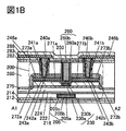
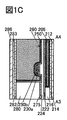
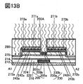
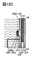
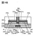
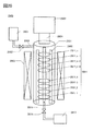
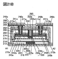
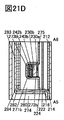
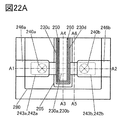
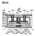
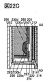
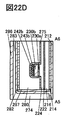
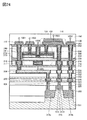
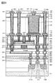
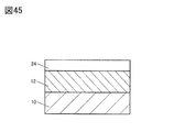
- One aspect of the present invention includes a semiconductor film, a pair of shielding films on the semiconductor film, and an insulating film located on the semiconductor film and provided between the pair of shielding films.
- a semiconductor device having a pair of n-type regions and an i-type region provided between a pair of n-type regions, the n-type region superimposing on a shielding film and the i-type region superimposing on an insulating film. Is.
- Another aspect of the present invention is located between the semiconductor film, the pair of shielding films on the semiconductor film, the protective film on the pair of shielding films, and the pair of shielding films. It has an insulating film, and the semiconductor film has a pair of n-type regions and an i-type region provided between the pair of n-type regions, and the n-type region overlaps with the shielding film and i.
- the mold region is a semiconductor device that overlaps with the insulating film.
- the protective film preferably has aluminum and oxygen. Further, in the above, it is preferable that the shielding film has a function of shielding electromagnetic waves of 300 MHz or more and 300 GHz or less. Further, in the above, it is preferable that the shielding film has tantalum and nitrogen.
- the i-type region has a carrier concentration of 1 ⁇ 10 -9 cm -3 or more and less than 1 ⁇ 10 17 cm -3
- the n-type region has a carrier concentration of 1 ⁇ 10 17 cm -3 or more and 1 ⁇ 10 It is preferably 21 cm -3 or less.
- the semiconductor film is preferably a metal oxide.
- the semiconductor film is preferably any one or a plurality selected from In, Ga, and Zn.
- the insulating film preferably has silicon and oxygen.
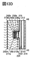
- Another aspect of the present invention is a first step of forming a semiconductor film, a second step of forming a shielding film on the semiconductor film, and a third step of processing the semiconductor film and the shielding film into an island shape.
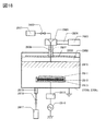
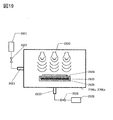
- microwave irradiation is preferably performed in a temperature range of 300 ° C. or higher and 500 ° C. or lower. Further, in the above, it is preferable that the microwave irradiation is performed in a pressure range of 300 Pa or more and 700 Pa or less.
- the heat treatment includes a first heat treatment and a second heat treatment, and the first heat treatment is performed in an oxygen atmosphere in a range of 300 ° C. or higher and 500 ° C. or lower.
- the second heat treatment is preferably carried out in a nitrogen atmosphere in a range of 300 ° C. or higher and 500 ° C. or lower. Further, in the above, it is preferable that the first heat treatment is performed for a longer time than the second heat treatment.
- the insulating film is preferably formed by using a plasma chemical vapor deposition method or an atomic layer deposition method.
- the semiconductor film has a metal oxide, the metal oxide has one or more selected from In, Ga, and Zn, and the metal oxide has a sputtering method and an atomic layer. It is preferably formed using a layer deposition method or a metalorganic vapor phase growth method.
- the ninth step is to form hafnium oxide by an atomic layer deposition method.
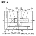
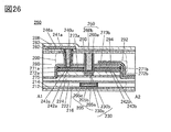
- an oxide film is formed on a substrate, a first conductive film is formed on the oxide film, and the oxide film and the first conductive film are processed into an island shape. , Oxide, and a first conductor, overlying the oxide and the first conductor to form a first insulator, and removing a portion of the first insulator to form an opening. Then, a part of the first conductor is removed by superimposing on the opening to form a second conductor and a third conductor, and between the second conductor and the third conductor.
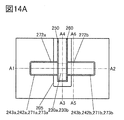
- a method for manufacturing a semiconductor device which forms a second insulator and a fourth conductor by performing CMP treatment on the insulating film and the second conductive film until the upper surface of the first insulator is exposed. Is.
- an oxide film is formed on a substrate, a first conductive film is formed on the oxide film, and the oxide film and the first conductive film are processed into an island shape. , Oxide, and a first conductor, overlying the oxide and the first conductor to form a first insulator, and removing a portion of the first insulator to form an opening. Then, a part of the first conductor is removed by superimposing on the opening to form a second conductor and a third conductor, and between the second conductor and the third conductor.
- the oxide is exposed in the region of the above, microwave-treated in an atmosphere containing oxygen, an insulating film is formed in contact with the upper surface of the oxide, and a second conductive film is formed on the insulating film.
- a method for manufacturing a semiconductor device which forms a second insulator and a fourth conductor by performing CMP treatment on the insulating film and the second conductive film until the upper surface of the first insulator is exposed. Is.
- an oxide film is formed on a substrate, a first conductive film is formed on the oxide film, and the oxide film and the first conductive film are processed into an island shape. , Oxide, and a first conductor, overlying the oxide and the first conductor to form a first insulator, and removing a portion of the first insulator to form an opening. Then, a part of the first conductor is removed by superimposing on the opening to form a second conductor and a third conductor, and between the second conductor and the third conductor.
- the oxide is exposed in the region of the above, subjected to microwave treatment in an atmosphere containing oxygen, is in contact with the upper surface of the oxide, a first insulating film is formed by the PEALD method, and is in contact with the upper surface of the first insulating film. Then, the second insulating film is formed by the thermal ALD method, the second conductive film is formed on the second insulating film, and the first insulating film, the second insulating film, and the second insulating film are formed. CMP treatment is performed on the conductive film until the upper surface of the first insulator is exposed to form a second insulator, a third insulator and a fourth conductor, and the third insulator is used. This is a method for manufacturing a semiconductor device, which is less likely to diffuse oxygen than the second insulator.
- the microwave treatment, the film formation of the first insulating film, and the film formation of the second insulating film are continuously processed without being exposed to the atmosphere.
- the first insulating film is an oxide film containing silicon and the second insulating film is an oxide film containing hafnium.
- the microwave treatment may be performed in an atmosphere containing oxygen, and the oxygen flow rate ratio may be larger than 0% and 100% or less. Further, in the above, it is preferable that the microwave treatment is performed in an atmosphere containing oxygen and argon, and the oxygen flow rate ratio is 10% or more and 40% or less.
- one aspect of the present invention it is possible to provide a semiconductor device having little variation in transistor characteristics.
- one aspect of the present invention can provide a semiconductor device with good reliability.
- one aspect of the present invention can provide a semiconductor device having good electrical characteristics.
- one aspect of the present invention can provide a semiconductor device having a large on-current.
- one aspect of the present invention can provide a semiconductor device capable of miniaturization or high integration.
- one aspect of the present invention can provide a low power consumption semiconductor device.
- FIG. 1A is a top view of a semiconductor device according to an aspect of the present invention.
- 1B to 1D are cross-sectional views of a semiconductor device according to an aspect of the present invention.
- FIG. 2 is a cross-sectional view of a semiconductor device according to an aspect of the present invention.
- FIG. 3A is a diagram illustrating classification of the crystal structure of IGZO.
- FIG. 3B is a diagram illustrating an XRD spectrum of a CAAC-IGZO film.
- FIG. 3C is a diagram for explaining the microelectron diffraction pattern of the CAAC-IGZO film.
- FIG. 4A is a top view showing a method for manufacturing a semiconductor device according to an aspect of the present invention.
- FIG. 4B to 4D are cross-sectional views showing a method of manufacturing a semiconductor device according to an aspect of the present invention.
- FIG. 5A is a top view showing a method for manufacturing a semiconductor device according to an aspect of the present invention.
- 5B to 5D are cross-sectional views showing a method of manufacturing a semiconductor device according to an aspect of the present invention.
- FIG. 6A is a top view showing a method for manufacturing a semiconductor device according to an aspect of the present invention.
- 6B to 6D are cross-sectional views showing a method of manufacturing a semiconductor device according to an aspect of the present invention.
- FIG. 7A is a top view showing a method for manufacturing a semiconductor device according to an aspect of the present invention.
- FIG. 7B to 7D are cross-sectional views showing a method of manufacturing a semiconductor device according to an aspect of the present invention.
- FIG. 8A is a top view showing a method for manufacturing a semiconductor device according to an aspect of the present invention.
- 8B to 8D are cross-sectional views showing a method of manufacturing a semiconductor device according to an aspect of the present invention.
- FIG. 9A is a top view showing a method for manufacturing a semiconductor device according to an aspect of the present invention.
- 9B to 9D are cross-sectional views showing a method of manufacturing a semiconductor device according to an aspect of the present invention.
- FIG. 10A is a top view showing a method for manufacturing a semiconductor device according to an aspect of the present invention.
- FIG. 10B to 10D are cross-sectional views showing a method of manufacturing a semiconductor device according to an aspect of the present invention.
- FIG. 11A is a top view showing a method for manufacturing a semiconductor device according to an aspect of the present invention.
- 11B to 11D are cross-sectional views showing a method of manufacturing a semiconductor device according to an aspect of the present invention.
- FIG. 12A is a top view showing a method for manufacturing a semiconductor device according to an aspect of the present invention.
- 12B to 12D are cross-sectional views showing a method of manufacturing a semiconductor device according to an aspect of the present invention.
- FIG. 13A is a top view showing a method for manufacturing a semiconductor device according to an aspect of the present invention.
- FIG. 13B to 13D are cross-sectional views showing a method of manufacturing a semiconductor device according to an aspect of the present invention.
- FIG. 14A is a top view showing a method for manufacturing a semiconductor device according to an aspect of the present invention.
- 14B to 14D are cross-sectional views showing a method of manufacturing a semiconductor device according to an aspect of the present invention.
- FIG. 15A is a top view showing a method for manufacturing a semiconductor device according to an aspect of the present invention.
- 15B to 15D are cross-sectional views showing a method of manufacturing a semiconductor device according to an aspect of the present invention.
- FIG. 16A is a top view showing a method for manufacturing a semiconductor device according to an aspect of the present invention.
- FIG. 16B to 16D are cross-sectional views showing a method of manufacturing a semiconductor device according to an aspect of the present invention.
- FIG. 17 is a top view illustrating a microwave processing apparatus according to an aspect of the present invention.
- FIG. 18 is a cross-sectional view illustrating a microwave processing apparatus according to an aspect of the present invention.
- FIG. 19 is a cross-sectional view illustrating a microwave processing apparatus according to an aspect of the present invention.
- FIG. 20 is a cross-sectional view illustrating a microwave processing apparatus according to an aspect of the present invention.
- FIG. 21A is a top view of a semiconductor device according to an aspect of the present invention.
- 21B to 21D are cross-sectional views of a semiconductor device according to an aspect of the present invention.
- FIG. 21A is a top view of a semiconductor device according to an aspect of the present invention.
- 21B to 21D are cross-sectional views of a semiconductor device according to an aspect of the present invention.
- FIG. 17
- 22A is a top view of a semiconductor device according to an aspect of the present invention.
- 22B to 22D are cross-sectional views of a semiconductor device according to an aspect of the present invention.
- 23A and 23B are cross-sectional views of a semiconductor device according to an aspect of the present invention.
- FIG. 24 is a cross-sectional view showing the configuration of a storage device according to an aspect of the present invention.
- FIG. 25 is a cross-sectional view showing the configuration of a storage device according to an aspect of the present invention.
- FIG. 26 is a cross-sectional view of a semiconductor device according to an aspect of the present invention.
- 27A and 27B are cross-sectional views of a semiconductor device according to an aspect of the present invention.
- FIG. 28 is a cross-sectional view of a semiconductor device according to an aspect of the present invention.
- FIG. 29 is a cross-sectional view of a semiconductor device according to an aspect of the present invention.
- FIG. 30A is a block diagram showing a configuration example of a storage device according to an aspect of the present invention.
- FIG. 30B is a schematic view showing a configuration example of a storage device according to an aspect of the present invention.
- 31A to 31H are circuit diagrams showing a configuration example of a storage device according to an aspect of the present invention.
- FIG. 32 is a diagram showing various storage devices for each layer.
- 33A and 33B are schematic views of a semiconductor device according to an aspect of the present invention.
- 34A and 34B are diagrams illustrating an example of an electronic component.
- 35A to 35E are schematic views of a storage device according to an aspect of the present invention.
- 36A to 36H are views showing an electronic device according to an aspect of the present invention.
- FIG. 37 is a diagram showing the electrical characteristics of the sample according to this embodiment.
- 38A to 38C are schematic views illustrating a method of calculating an operating frequency according to the present embodiment.
- FIG. 39 is a diagram showing the result of calculating the operating frequency of the sample according to this embodiment.
- 40A and 40B are diagrams showing the electrical characteristics of the sample according to this embodiment.
- 41A and 41B are schematic views of a sample according to this embodiment.
- 42A and 42B are diagrams showing the sheet resistance of the sample according to this embodiment.
- 43A and 43B are diagrams showing the sheet resistance of the sample according to this embodiment.
- FIG. 44A and 44B are diagrams showing the hydrogen concentration of the sample according to this example.
- FIG. 45 is a schematic diagram of a sample according to this embodiment.
- FIG. 46 is a diagram showing the carrier concentration of the sample according to this example.
- FIG. 47 is a schematic diagram of a sample according to this embodiment.
- 48A and 48B are diagrams showing CPM spectra of samples according to this example.
- FIG. 49A is a diagram showing the absorption coefficient of the sample according to this embodiment.
- FIG. 49B is a diagram showing the carrier concentration of the sample according to this example.
- FIG. 50A is a diagram showing the absorption coefficient of the sample according to this embodiment.
- FIG. 50B is a diagram showing the carrier concentration of the sample according to this example.
- FIG. 51 is a schematic diagram of a sample according to this embodiment.
- FIG. 52 is a cross-sectional STEM image of the sample according to this embodiment.
- 53A and 53B are SCM polarity images of the sample according to
- the size, layer thickness, or area may be exaggerated for clarity. Therefore, it is not necessarily limited to that scale.
- the drawings schematically show ideal examples, and are not limited to the shapes or values shown in the drawings. For example, in an actual manufacturing process, layers, resist masks, etc. may be unintentionally reduced due to processing such as etching, but they may not be reflected in the figure for the sake of easy understanding. Further, in the drawings, the same reference numerals may be used in common between different drawings for the same parts or parts having similar functions, and the repeated description thereof may be omitted. Further, when referring to the same function, the hatch pattern may be the same and no particular sign may be added.
- a top view also referred to as a "plan view”
- a perspective view the description of some components may be omitted.
- some hidden lines may be omitted.
- the ordinal numbers attached as the first, second, etc. are used for convenience, and do not indicate the process order or the stacking order. Therefore, for example, the "first” can be appropriately replaced with the “second” or “third” for explanation.
- the ordinal numbers described in the present specification and the like may not match the ordinal numbers used to specify one aspect of the present invention.
- X and Y are connected, the case where X and Y are electrically connected and the case where X and Y function. It is assumed that the case where X and Y are directly connected and the case where X and Y are directly connected are disclosed in the present specification and the like. Therefore, it is not limited to the predetermined connection relationship, for example, the connection relationship shown in the figure or text, and other than the connection relationship shown in the figure or text, it is assumed that the connection relationship is disclosed in the figure or text.
- X and Y are assumed to be objects (for example, devices, elements, circuits, wirings, electrodes, terminals, conductive films, layers, etc.).
- a transistor is an element having at least three terminals including a gate, a drain, and a source. It also has a region (hereinafter, also referred to as a channel forming region) in which a channel is formed between the drain (drain terminal, drain region or drain electrode) and the source (source terminal, source region or source electrode). A current can flow between the source and the drain through the channel formation region.
- the channel formation region means a region in which a current mainly flows.
- source and drain may be interchanged with each other. Therefore, in the present specification and the like, the terms source and drain may be used interchangeably.
- the channel length is, for example, the source in the top view of the transistor, the region where the semiconductor (or the portion where the current flows in the semiconductor when the transistor is on) and the gate electrode overlap each other, or the channel formation region.
- the channel length does not always take the same value in all regions. That is, the channel length of one transistor may not be fixed to one value. Therefore, in the present specification, the channel length is set to any one value, the maximum value, the minimum value, or the average value in the channel formation region.
- the channel width is, for example, the channel length direction in the region where the semiconductor (or the portion where the current flows in the semiconductor when the transistor is on) and the gate electrode overlap each other in the top view of the transistor, or the channel formation region. Refers to the length of the channel formation region in the vertical direction with reference to. In one transistor, the channel width does not always take the same value in all regions. That is, the channel width of one transistor may not be fixed to one value. Therefore, in the present specification, the channel width is set to any one value, the maximum value, the minimum value, or the average value in the channel formation region.
- the channel width in the region where the channel is actually formed (hereinafter, also referred to as “effective channel width”) and the channel width shown in the top view of the transistor. (Hereinafter, also referred to as “apparent channel width”) and may be different.
- the effective channel width may be larger than the apparent channel width, and the influence thereof may not be negligible.
- the proportion of the channel forming region formed on the side surface of the semiconductor may be large. In that case, the effective channel width is larger than the apparent channel width.
- channel width may refer to the apparent channel width.
- channel width may refer to an effective channel width.
- the channel length, channel width, effective channel width, apparent channel width, and the like can be determined by analyzing a cross-sectional TEM image or the like.
- the semiconductor impurities are, for example, other than the main components constituting the semiconductor.
- an element having a concentration of less than 0.1 atomic% can be said to be an impurity. Due to the inclusion of impurities, for example, the defect level density of the semiconductor may increase or the crystallinity may decrease.
- the impurities that change the characteristics of the semiconductor include, for example, Group 1 elements, Group 2 elements, Group 13 elements, Group 14 elements, Group 15 elements, and oxide semiconductors.
- transition metals other than the main component such as hydrogen, lithium, sodium, silicon, boron, phosphorus, carbon, and nitrogen. Water may also function as an impurity.
- the oxide semiconductor to an oxygen vacancy V O: also referred to as oxygen vacancy
- the oxide nitride has a higher oxygen content than nitrogen as its composition.
- silicon oxide has a higher oxygen content than nitrogen in its composition.
- the nitride oxide has a higher nitrogen content than oxygen in its composition.
- silicon nitride has a higher nitrogen content than oxygen in its composition.
- the term “insulator” can be paraphrased as an insulating film or an insulating layer.
- the term “conductor” can be rephrased as a conductive film or a conductive layer.
- semiconductor can be paraphrased as a semiconductor film or a semiconductor layer.
- parallel means a state in which two straight lines are arranged at an angle of -10 degrees or more and 10 degrees or less. Therefore, the case of -5 degrees or more and 5 degrees or less is also included.
- approximately parallel means a state in which two straight lines are arranged at an angle of -30 degrees or more and 30 degrees or less.
- vertical means a state in which two straight lines are arranged at an angle of 80 degrees or more and 100 degrees or less. Therefore, the case of 85 degrees or more and 95 degrees or less is also included.
- approximately vertical means a state in which two straight lines are arranged at an angle of 60 degrees or more and 120 degrees or less.
- a metal oxide is a metal oxide in a broad sense. Metal oxides are classified into oxide insulators, oxide conductors (including transparent oxide conductors), oxide semiconductors (also referred to as Oxide Semiconductor or simply OS) and the like. For example, when a metal oxide is used in the semiconductor layer of a transistor, the metal oxide may be referred to as an oxide semiconductor. That is, when it is described as an OS transistor, it can be rephrased as a transistor having a metal oxide or an oxide semiconductor.
- normally off means that when a potential is not applied to the gate or a ground potential is applied to the gate, the drain current per 1 ⁇ m of the channel width flowing through the transistor is 1 ⁇ 10 ⁇ at room temperature. It means that it is 20 A or less, 1 ⁇ 10 -18 A or less at 85 ° C, or 1 ⁇ 10 -16 A or less at 125 ° C.
- FIG. 1A is a top view of the semiconductor device.
- 1B to 1D are cross-sectional views of the semiconductor device.
- FIG. 1B is a cross-sectional view of the portion shown by the alternate long and short dash line of A1-A2 in FIG. 1A, and is also a cross-sectional view of the transistor 200 in the channel length direction.
- FIG. 1C is a cross-sectional view of the portion shown by the alternate long and short dash line of A3-A4 in FIG. 1A, and is also a cross-sectional view of the transistor 200 in the channel width direction.
- FIG. 1D is a cross-sectional view of the portion shown by the alternate long and short dash line in FIG. 1A.
- some elements are omitted for the purpose of clarifying the figure.
- the semiconductor device of one aspect of the present invention includes an insulator 212 on a substrate (not shown), an insulator 214 on the insulator 212, a transistor 200 on the insulator 214, and an insulator 280 on the transistor 200. It has an insulator 282 on an insulator 280 and an insulator 283 on an insulator 282.
- the insulator 212, the insulator 214, the insulator 280, the insulator 282, and the insulator 283 function as an interlayer film. Further, it has a conductor 240 (conductor 240a and conductor 240b) that is electrically connected to the transistor 200 and functions as a plug.
- An insulator 241 (insulator 241a and insulator 241b) is provided in contact with the side surface of the conductor 240 that functions as a plug. Further, on the insulator 283 and on the conductor 240, a conductor 246 (conductor 246a and a conductor 246b) that is electrically connected to the conductor 240 and functions as wiring is provided. Further, an insulator 286 is provided on the conductor 246 and the insulator 283.
- the insulator 241a is provided in contact with the inner wall of the opening of the insulator 280, the insulator 282, and the insulator 283, and the first conductor of the conductor 240a is provided in contact with the side surface of the insulator 241a, and further inside.
- a second conductor of the conductor 240a is provided.
- the insulator 241b is provided in contact with the inner wall of the opening of the insulator 280, the insulator 282, and the insulator 283, and the first conductor of the conductor 240b is provided in contact with the side surface of the insulator 241b.
- a second conductor of the conductor 240b is provided inside.
- the height of the upper surface of the conductor 240 and the height of the upper surface of the insulator 283 in the region overlapping the conductor 246 can be made about the same.
- the transistor 200 shows a configuration in which the first conductor of the conductor 240 and the second conductor of the conductor 240 are laminated, but the present invention is not limited to this.
- the conductor 240 may be provided as a single layer or a laminated structure having three or more layers. When the structure has a laminated structure, an ordinal number may be given in the order of formation to distinguish them.
- the transistor 200 includes an insulator 216 on the insulator 214 and a conductor 205 (conductor 205a, conductor 205b, and conductor 205) arranged so as to be embedded in the insulator 216. 205c), the insulator 222 on the insulator 216 and the conductor 205, the insulator 224 on the insulator 222, the oxide 230a on the insulator 224, and the oxide 230b on the oxide 230a.
- Oxide 243 on the oxide 230b (oxide 243a and oxide 243b), the conductor 242a on the oxide 243a, the insulator 271a on the conductor 242a, and the insulator 273a on the insulator 271a.
- Conductor 260 (conductor 260a and conductor 260b) that overlaps a part of 230b, insulator 272a that contacts the side surface of oxide 230b, the side surface of oxide 243a, and the side surface of conductor 242a, and the side surface of oxide 230b.
- Insulator 272b in contact with the side surface of the oxide 243b and the side surface of the conductor 242b, and the insulator 224, the insulator 272a, the insulator 272b, the insulator 273a, and the insulator 275 arranged on the insulator 273b.
- the upper surface of the conductor 260 is substantially aligned in height with at least a part of the upper surface of the insulator 250 and at least a part of the upper surface of the insulator 280. Be placed. Further, the insulator 282 is in contact with at least a part of the upper surfaces of the conductor 260, the insulator 250, and the insulator 280.
- the oxide 230a and the oxide 230b may be collectively referred to as the oxide 230.
- the insulator 271a and the insulator 271b may be collectively referred to as an insulator 271.
- the insulator 272a and the insulator 272b may be collectively referred to as an insulator 272.
- the insulator 273a and the insulator 273b may be collectively referred to as an insulator 273.
- the conductor 242a and the conductor 242b may be collectively referred to as a conductor 242.
- the insulator 280 and the insulator 275 are provided with an opening reaching the oxide 230b.
- An insulator 250 and a conductor 260 are arranged in the opening. Further, in the channel length direction of the transistor 200, the conductor 260 is between the insulator 271a, the insulator 273a, the conductor 242a and the oxide 243a, and the insulator 271b, the insulator 273b, the conductor 242b and the oxide 243b.
- an insulator 250 is provided.
- the insulator 250 has a region in contact with the side surface of the conductor 260 and a region in contact with the bottom surface of the conductor 260.
- the oxide 230 preferably has an oxide 230a arranged on the insulator 224 and an oxide 230b arranged on the oxide 230a.
- the oxide 230a By having the oxide 230a under the oxide 230b, it is possible to suppress the diffusion of impurities into the oxide 230b from the structure formed below the oxide 230a.
- the present invention is not limited to this.
- a single layer of the oxide 230b or a laminated structure of three or more layers may be provided, or each of the oxide 230a and the oxide 230b may have a laminated structure.
- the conductor 260 functions as a first gate (also referred to as a top gate) electrode, and the conductor 205 functions as a second gate (also referred to as a back gate) electrode.
- the insulator 250 functions as a first gate insulator, and the insulator 224 functions as a second gate insulator.
- the conductor 242a functions as one of the source and the drain, and the conductor 242b functions as the other of the source and the drain. Further, at least a part of the region of the oxide 230 overlapping with the conductor 260 functions as a channel forming region.
- the oxide 230b is provided so as to sandwich a region 230bc that functions as a channel forming region of the transistor 200 and a pair of regions 230ba and a region 230bb that function as a source region or a drain region. And have. At least a part of the region 230bc overlaps with the conductor 260.
- the region 230bc is provided in the region between the pair of conductors 242a and the conductors 242b.
- the region 230ba is provided so as to be superimposed on the conductor 242a, and the region 230bb is provided so as to be superimposed on the conductor 242b.
- the region 230bc that functions as a channel forming region is a high resistance region having a low carrier concentration because it has less oxygen deficiency or a lower impurity concentration than the regions 230ba and 230bb.
- the region 230ba and the region 230bb that function as the source region or the drain region are regions in which the carrier concentration is increased and the resistance is lowered due to a large amount of oxygen deficiency or a high concentration of impurities such as hydrogen, nitrogen and metal elements. is there. That is, the region 230ba and the region 230bb are regions having a high carrier concentration and low resistance as compared with the region 230bc.
- the carrier concentration of the region 230 bc that functions as the channel forming region is preferably 1 ⁇ 10 18 cm -3 or less, more preferably less than 1 ⁇ 10 17 cm -3 , and 1 ⁇ 10 16 cm. It is more preferably less than -3 , still more preferably less than 1 ⁇ 10 13 cm -3 , and even more preferably less than 1 ⁇ 10 12 cm -3 .
- the lower limit of the carrier concentration in the region 230 bc that functions as the channel formation region is not particularly limited, but may be, for example, 1 ⁇ 10 -9 cm -3 .
- the carrier concentration of the region 230ba and the region 230bb that function as the source region or the drain region is preferably, for example, 1 ⁇ 10 17 cm -3 or more, and more preferably 1 ⁇ 10 18 cm -3 or more. It is more preferably 1 ⁇ 10 19 cm -3 or more.
- the upper limit of the carrier concentration of the region 230ba and the region 230bb that function as the source region or the drain region is not particularly limited, but may be, for example, 1 ⁇ 10 21 cm -3 .
- the carrier concentration is equal to or lower than the carrier concentration of the region 230ba and the region 230bb, and equal to or higher than the carrier concentration of the region 230bb.
- Regions may be formed. That is, the region functions as a junction region between the region 230bc and the region 230ba or the region 230bb.
- the hydrogen concentration may be equal to or lower than the hydrogen concentration in the region 230ba and 230bb, and may be equal to or higher than the hydrogen concentration in the region 230bc.
- the junction region may have an oxygen deficiency equal to or less than that of the region 230ba and 230bb, and may be equal to or greater than that of the region 230bc.
- FIG. 2 shows an example in which the region 230ba, the region 230bb, and the region 230bc are formed on the oxide 230b, but the present invention is not limited to this.
- each of the above regions may be formed not only with the oxide 230b but also with the oxide 230a.
- concentrations of the metal elements detected in each region and the impurity elements such as hydrogen and nitrogen are not limited to the stepwise changes in each region, but may be continuously changed in each region. That is, the closer the region is to the channel formation region, the lower the concentration of metal elements and impurity elements such as hydrogen and nitrogen is sufficient.
- a metal oxide hereinafter, also referred to as an oxide semiconductor that functions as a semiconductor for the oxide 230 (oxide 230a and oxide 230b) containing the channel forming region.
- the metal oxide that functions as a semiconductor it is preferable to use a metal oxide having a band gap of 2 eV or more, preferably 2.5 eV or more. As described above, by using a metal oxide having a large bandgap, the off-current of the transistor can be reduced.
- an In-M-Zn oxide having indium, element M and zinc (element M is aluminum, gallium, yttrium, tin, copper, vanadium, beryllium, boron, titanium, iron, nickel, germanium).
- Zinc, molybdenum, lanthanum, cerium, neodymium, hafnium, tantalum, tungsten, magnesium, etc. (one or more) and the like may be used.
- an In-Ga oxide, an In-Zn oxide, or an indium oxide may be used as the oxide 230.
- the atomic number ratio of In to the element M in the metal oxide used for the oxide 230b is larger than the atomic number ratio of In to the element M in the metal oxide used for the oxide 230a.
- the oxide 230a under the oxide 230b By arranging the oxide 230a under the oxide 230b in this way, it is possible to suppress the diffusion of impurities and oxygen from the structure formed below the oxide 230a to the oxide 230b. ..
- the oxide 230a and the oxide 230b have a common element (main component) other than oxygen, the defect level density at the interface between the oxide 230a and the oxide 230b can be lowered. Since the defect level density at the interface between the oxide 230a and the oxide 230b can be lowered, the influence of interfacial scattering on carrier conduction is small, and a high on-current can be obtained.
- each oxide 230b has crystallinity.
- CAAC-OS c-axis aligned crystalline semiconductor semiconductor
- CAAC-OS is a metal oxide having a highly crystalline and dense structure and having few impurities and defects (for example, oxygen deficiency ( VO )).
- the CAAC-OS is subjected to heat treatment at a temperature at which the metal oxide does not undergo polycrystallization (for example, 400 ° C. or higher and 600 ° C. or lower), whereby CAAC-OS has a more crystalline and dense structure. Can be.
- a temperature at which the metal oxide does not undergo polycrystallization for example, 400 ° C. or higher and 600 ° C. or lower
- the metal oxide having CAAC-OS has stable physical properties. Therefore, the metal oxide having CAAC-OS is resistant to heat and has high reliability.
- Transistors using oxide semiconductors may have poor electrical characteristics and poor reliability if impurities or oxygen deficiencies are present in the region where channels are formed in the oxide semiconductor.
- the hydrogen of oxygen vacancies near defects containing the hydrogen to the oxygen deficiency (hereinafter, may be referred to as V O H.)
- V O H defects containing the hydrogen to the oxygen deficiency
- the transistor has normal-on characteristics (the channel exists even if no voltage is applied to the gate electrode, and the current is applied to the transistor. Flowing characteristics). Therefore, in the region where a channel of the oxide semiconductor is formed, impurities, oxygen deficiency, and V O H it is preferred to be reduced as much as possible.
- the region in which the channel is formed in the oxide semiconductor is preferably i-type (intrinsicized) or substantially i-type with a reduced carrier concentration.
- excess oxygen an insulator containing oxygen desorbed by heating
- the oxide semiconductor is separated from the insulator.
- oxygen is supplied, it is possible to reduce oxygen vacancies, and V O H to.
- the on-current of the transistor 200 may decrease or the field effect mobility may decrease.
- the oxygen supplied to the source region or the drain region varies in the surface of the substrate, so that the characteristics of the semiconductor device having the transistor vary.
- the region 230bc that functions as the channel forming region preferably has an i-type or substantially i-type with a reduced carrier concentration.
- the region 230ba and the region 230bb that function as the source region or the drain region have a high carrier concentration and are preferably n-type.
- the oxygen deficiency in the oxide semiconductor region 230Bc, and reduces V O H it is preferred that an excess amount of oxygen in the region 230ba and region 230bb to not be supplied.
- the microwave processing refers to processing using, for example, a device having a power source that generates high-density plasma using microwaves.
- the microwave may refer to an electromagnetic wave having a frequency of 300 MHz or more and 300 GHz or less.
- oxygen gas By performing microwave treatment in an atmosphere containing oxygen, oxygen gas can be turned into plasma using microwaves or high frequencies such as RF, and the oxygen plasma can be allowed to act. At this time, the region 230bc can be irradiated with a high frequency such as microwave or RF. Plasma, by the action such as a microwave, it is possible to divide the V O H region 230Bc. Thus, the hydrogen H is removed from the region 230Bc, it is possible to fill oxygen vacancies V O in oxygen. That is, in the region 230Bc, happening reaction of "V O H ⁇ H + V O", it is possible to reduce the hydrogen concentration in the regions 230Bc. Therefore, to reduce oxygen vacancies, and V O H in the region 230Bc, the carrier concentration can be decreased.
- the action of microwaves, high frequencies such as RF, oxygen plasma, etc. is shielded by the conductors 242a and 242b and does not reach the regions 230ba and 230bb. That is, the conductor 242 functions as a shielding film against microwaves, high frequencies such as RF, oxygen plasma, and the like. Further, the action of the oxygen plasma can be reduced by the insulator 271, the insulator 273, the insulator 275, and the insulator 280, which are provided so as to cover the oxide 230b and the conductor 242. Thus, during the microwave treatment, the region 230ba and area 230Bb, reduction of V O H, and excessive amount of oxygen supply does not occur, it is possible to prevent a decrease in carrier concentration.
- the oxide selectively oxygen deficiency in the semiconductor region 230Bc, a and V O H may be removed to an area 230Bc i-type or substantially i-type. Further, it is possible to suppress the supply of excess oxygen to the region 230ba and the region 230bb that function as the source region or the drain region, and maintain the n-type. As a result, fluctuations in the electrical characteristics of the transistor 200 can be suppressed, and fluctuations in the electrical characteristics of the transistor 200 can be suppressed within the substrate surface.
- the side surface of the opening in which the conductor 260 and the like are embedded is substantially perpendicular to the surface to be formed of the oxide 230b, including the groove portion of the oxide 230b. It is not limited to this.
- the bottom of the opening may have a gently curved surface and may have a U-shape.
- the side surface of the opening may be inclined with respect to the surface to be formed of the oxide 230b.
- a curved surface may be provided between the side surface of the oxide 230b and the upper surface of the oxide 230b in a cross-sectional view of the transistor 200 in the channel width direction. That is, the end of the side surface and the end of the upper surface may be curved (also referred to as a round shape).
- the radius of curvature on the curved surface is preferably larger than 0 nm, smaller than the film thickness of the oxide 230b in the region overlapping the conductor 242, or smaller than half the length of the region having no curved surface.
- the radius of curvature on the curved surface is larger than 0 nm and 20 nm or less, preferably 1 nm or more and 15 nm or less, and more preferably 2 nm or more and 10 nm or less.
- the oxide 230 preferably has a laminated structure of a plurality of oxide layers having different chemical compositions.
- the atomic number ratio of the element M to the metal element as the main component is the ratio of the element M to the metal element as the main component in the metal oxide used for the oxide 230b. It is preferably larger than the atomic number ratio.
- the atomic number ratio of the element M to In is preferably larger than the atomic number ratio of the element M to In in the metal oxide used for the oxide 230b.
- the atomic number ratio of In to the element M is preferably larger than the atomic number ratio of In to the element M in the metal oxide used for the oxide 230a.
- the oxide 230b is preferably an oxide having crystallinity such as CAAC-OS.
- Crystalline oxides such as CAAC-OS have a dense structure with high crystallinity with few impurities and defects (oxygen deficiency, etc.). Therefore, it is possible to suppress the extraction of oxygen from the oxide 230b by the source electrode or the drain electrode. As a result, oxygen can be reduced from being extracted from the oxide 230b even if heat treatment is performed, so that the transistor 200 is stable against a high temperature (so-called thermal budget) in the manufacturing process.
- the lower end of the conduction band changes gently.
- the lower end of the conduction band at the junction between the oxide 230a and the oxide 230b is continuously changed or continuously bonded. In order to do so, it is preferable to reduce the defect level density of the mixed layer formed at the interface between the oxide 230a and the oxide 230b.
- the oxide 230a and the oxide 230b have a common element other than oxygen as a main component, a mixed layer having a low defect level density can be formed.
- the oxide 230b is an In-M-Zn oxide
- the oxide 230a is an In-M-Zn oxide, an M-Zn oxide, an element M oxide, an In-Zn oxide, or an indium oxide. Etc. may be used.
- a metal oxide having a composition in the vicinity thereof may be used.
- a metal oxide having a composition may be used.
- the composition in the vicinity includes a range of ⁇ 30% of the desired atomic number ratio.
- the above atomic number ratio is not limited to the atomic number ratio of the formed metal oxide, but is the atomic number ratio of the sputtering target used for forming the metal oxide. It may be.
- the defect level density at the interface between the oxide 230a and the oxide 230b can be lowered. Therefore, the influence of interfacial scattering on carrier conduction is reduced, and the transistor 200 can obtain a large on-current and high frequency characteristics.
- At least one of the insulator 212, the insulator 214, the insulator 271, the insulator 272, the insulator 275, the insulator 282, the insulator 283, and the insulator 286 has impurities such as water and hydrogen from the substrate side or , It is preferable to function as a barrier insulating film that suppresses diffusion from above the transistor 200 to the transistor 200. Therefore, at least one of insulator 212, insulator 214, insulator 271, insulator 272, insulator 275, insulator 282, insulator 283, and insulator 286 is a hydrogen atom, a hydrogen molecule, a water molecule, and a nitrogen atom.
- molecular nitrogen, nitric oxide molecule (N 2 O, NO, etc. NO 2), it has a function of suppressing the diffusion of impurities such as copper atoms (hardly the impurity is transmitted) it is preferable to use an insulating material.
- an insulating material having a function of suppressing the diffusion of oxygen for example, at least one oxygen atom, oxygen molecule, etc. (the oxygen is difficult to permeate).
- the barrier insulating film refers to an insulating film having a barrier property.
- the barrier property refers to a function of suppressing the diffusion of the corresponding substance (also referred to as low permeability). Alternatively, it refers to the function of capturing and fixing (also called gettering) the corresponding substance.
- Examples of the insulator 212, insulator 214, insulator 271, insulator 272, insulator 275, insulator 282, insulator 283, and insulator 286 include aluminum oxide, magnesium oxide, hafnium oxide, gallium oxide, and indium oxide. Gallium zinc oxide, silicon nitride, silicon nitride oxide and the like can be used.
- the insulator 214, the insulator 275, and the insulator 282 it is preferable to use aluminum oxide or magnesium oxide having a high function of capturing hydrogen and fixing hydrogen.
- impurities such as water and hydrogen from diffusing from the substrate side to the transistor 200 side via the insulator 212 and the insulator 214.
- impurities such as water and hydrogen from diffusing to the transistor 200 side from the interlayer insulating film or the like arranged outside the insulator 286.
- the transistor 200 is insulated from the insulator 212, the insulator 214, the insulator 271, the insulator 272, the insulator 275, the insulator 282, and the insulator having a function of suppressing the diffusion of impurities such as water and hydrogen and oxygen. It is preferable that the structure is surrounded by the body 283 and the insulator 286.
- a metal oxide such as AlO x (x is an arbitrary number larger than 0) or MgO y (y is an arbitrary number larger than 0).
- an oxygen atom has a dangling bond, and the dangling bond may have a property of capturing or fixing hydrogen.
- a metal oxide having such an amorphous structure as a component of the transistor 200 or providing it around the transistor 200, hydrogen contained in the transistor 200 or hydrogen existing around the transistor 200 is captured or fixed. be able to. In particular, it is preferable to capture or fix hydrogen contained in the channel forming region of the transistor 200.
- a metal oxide having an amorphous structure as a component of the transistor 200 or providing it around the transistor 200, the transistor 200 having good characteristics and high reliability and a semiconductor device can be manufactured.
- the insulator 212, the insulator 214, the insulator 271, the insulator 272, the insulator 275, the insulator 282, the insulator 283, and the insulator 286 preferably have an amorphous structure, but some of them are polycrystalline. Areas of structure may be formed. Further, the insulator 212, the insulator 214, the insulator 271, the insulator 272, the insulator 275, the insulator 282, the insulator 283, and the insulator 286 include a layer having an amorphous structure and a layer having a polycrystalline structure. It may have a laminated multi-layer structure. For example, it may be a laminated structure in which a layer having a polycrystalline structure is formed on a layer having an amorphous structure.
- the film formation of the insulator 212, the insulator 214, the insulator 271, the insulator 272, the insulator 275, the insulator 282, the insulator 283, and the insulator 286 may be performed by using, for example, a sputtering method. Since hydrogen does not have to be used as the film forming gas in the sputtering method, hydrogen in the insulator 212, the insulator 214, the insulator 271, the insulator 272, the insulator 275, the insulator 282, the insulator 283, and the insulator 286. The concentration can be reduced.
- the film forming method is not limited to the sputtering method, but is limited to a chemical vapor deposition (CVD) method, a molecular beam epitaxy (MBE) method, and a pulsed laser deposition (PLD: Pulsed Laser Deposition) method.
- CVD chemical vapor deposition
- MBE molecular beam epitaxy
- PLD pulsed laser deposition
- Method atomic layer deposition (ALD: Atomic Layer Deposition) method and the like may be appropriately used.
- the resistivity of the insulator 212, the insulator 283, and the insulator 286 may be preferable to reduce the resistivity of the insulator 212, the insulator 283, and the insulator 286.
- the resistivity of the insulator 212, the insulator 283, and the insulator 286 is preferably 1 ⁇ 10 10 ⁇ cm or more and 1 ⁇ 10 15 ⁇ cm or less.
- the insulator 216 and the insulator 280 have a lower dielectric constant than the insulator 214.
- a material having a low dielectric constant as an interlayer film, it is possible to reduce the parasitic capacitance generated between the wirings.
- the conductor 205 is arranged so as to overlap the oxide 230 and the conductor 260.
- the conductor 205 is embedded in the opening formed in the insulator 216.
- a part of the conductor 205 may be provided so as to be embedded in the insulator 214.
- the conductor 205 has a conductor 205a, a conductor 205b, and a conductor 205c.
- the conductor 205a is provided in contact with the bottom surface and the side wall of the opening.
- the conductor 205b is provided so as to be embedded in the recess formed in the conductor 205a.
- the upper surface of the conductor 205b is lower than the upper surface of the conductor 205a and the upper surface of the insulator 216.
- the conductor 205c is provided in contact with the upper surface of the conductor 205b and the side surface of the conductor 205a.
- the height of the upper surface of the conductor 205c is substantially the same as the height of the upper surface of the conductor 205a and the height of the upper surface of the insulator 216. That is, the conductor 205b is wrapped in the conductor 205a and the conductor 205c.
- the conductors 205a and conductors 205c are hydrogen atoms, hydrogen molecules, water molecules, nitrogen atom, a nitrogen molecule, nitric oxide molecule (N 2 O, NO, etc. NO 2), the diffusion of impurities such as copper atoms It is preferable to use a conductive material having a suppressing function. Alternatively, it is preferable to use a conductive material having a function of suppressing the diffusion of oxygen (for example, at least one oxygen atom, oxygen molecule, etc.).
- the conductor 205a and the conductor 205c By using a conductive material having a function of reducing the diffusion of hydrogen for the conductor 205a and the conductor 205c, impurities such as hydrogen contained in the conductor 205b are transferred to the oxide 230 via the insulator 224 and the like. It can be prevented from spreading. Further, by using a conductive material having a function of suppressing the diffusion of oxygen for the conductor 205a and the conductor 205c, it is possible to prevent the conductor 205b from being oxidized and the conductivity from being lowered.
- the conductive material having a function of suppressing the diffusion of oxygen for example, titanium, titanium nitride, tantalum, tantalum nitride, ruthenium, ruthenium oxide and the like are preferably used. Therefore, as the conductor 205a and the conductor 205c, the conductive material may be a single layer or a laminate. For example, titanium nitride may be used for the conductor
- the conductor 205b it is preferable to use a conductive material containing tungsten, copper, or aluminum as a main component.
- tungsten may be used for the conductor 205b.
- the conductor 205 may function as a second gate electrode.
- the threshold voltage (Vth) of the transistor 200 can be controlled by changing the potential applied to the conductor 205 independently without interlocking with the potential applied to the conductor 260.
- Vth threshold voltage
- the electrical resistivity of the conductor 205 is designed in consideration of the potential applied to the conductor 205, and the film thickness of the conductor 205 is set according to the electrical resistivity. Further, the film thickness of the insulator 216 is almost the same as that of the conductor 205. Here, it is preferable to reduce the film thickness of the conductor 205 and the insulator 216 as much as the design of the conductor 205 allows. By reducing the thickness of the insulator 216, the absolute amount of impurities such as hydrogen contained in the insulator 216 can be reduced, so that the impurities can be reduced from diffusing into the oxide 230. ..
- the conductor 205 may be provided larger than the size of the region that does not overlap with the conductor 242a and the conductor 242b of the oxide 230.
- the conductor 205 is also stretched in a region outside the end portion of the oxide 230a and the oxide 230b intersecting the channel width direction. That is, it is preferable that the conductor 205 and the conductor 260 are superimposed via an insulator on the outside of the side surface of the oxide 230 in the channel width direction.
- the channel forming region of the oxide 230 is electrically surrounded by the electric field of the conductor 260 that functions as the first gate electrode and the electric field of the conductor 205 that functions as the second gate electrode. Can be done.
- the structure of the transistor that electrically surrounds the channel forming region by the electric fields of the first gate and the second gate is referred to as a surroundd channel (S-channel) structure.
- the transistor having the S-channel structure represents the structure of the transistor that electrically surrounds the channel formation region by the electric fields of one and the other of the pair of gate electrodes.
- the S-channel structure disclosed in the present specification and the like is different from the Fin type structure and the planar type structure.
- the conductor 205 is stretched to function as wiring.
- the present invention is not limited to this, and a conductor that functions as wiring may be provided under the conductor 205. Further, it is not always necessary to provide one conductor 205 for each transistor. For example, the conductor 205 may be shared by a plurality of transistors.
- the conductor 205 shows a configuration in which the conductor 205a, the conductor 205b, and the conductor 205c are laminated, but the present invention is not limited to this.
- the conductor 205 may be provided as a single-layer, two-layer, or four-layer or higher laminated structure. For example, it may have a two-layer structure of the conductor 205a and the conductor 205b.
- the insulator 222 and the insulator 224 function as a gate insulator.
- the insulator 222 has a function of suppressing the diffusion of hydrogen (for example, at least one hydrogen atom, hydrogen molecule, etc.). Further, the insulator 222 preferably has a function of suppressing the diffusion of oxygen (for example, at least one oxygen atom, oxygen molecule, etc.). For example, the insulator 222 preferably has a function of suppressing the diffusion of one or both of hydrogen and oxygen more than the insulator 224.
- the insulator 222 it is preferable to use an insulator containing oxides of one or both of aluminum and hafnium, which are insulating materials.
- the insulator it is preferable to use aluminum oxide, hafnium oxide, an oxide containing aluminum and hafnium (hafnium aluminate) and the like.
- the insulator 222 releases oxygen from the oxide 230 to the substrate side and diffuses impurities such as hydrogen from the peripheral portion of the transistor 200 to the oxide 230. Functions as a layer that suppresses.
- the insulator 222 it is possible to suppress the diffusion of impurities such as hydrogen into the inside of the transistor 200 and suppress the generation of oxygen deficiency in the oxide 230. Further, it is possible to suppress the conductor 205 from reacting with the oxygen contained in the insulator 224 and the oxide 230.
- aluminum oxide, bismuth oxide, germanium oxide, niobium oxide, silicon oxide, titanium oxide, tungsten oxide, yttrium oxide, and zirconium oxide may be added to the insulator.
- these insulators may be nitrided.
- the insulator 222 may be used by laminating silicon oxide, silicon nitride or silicon nitride on these insulators.
- the insulator 222 includes, for example, aluminum oxide, hafnium oxide, tantalum oxide, zirconium oxide, lead zirconate titanate (PZT), strontium titanate (SrTIO 3 ), (Ba, Sr) TiO 3 (BST) and the like. Insulators containing so-called high-k materials may be used in single layers or in layers. As the miniaturization and high integration of transistors progress, problems such as leakage current may occur due to the thinning of the gate insulator. By using a high-k material for an insulator that functions as a gate insulator, it is possible to reduce the gate potential during transistor operation while maintaining the physical film thickness.
- the insulator 224 in contact with the oxide 230 preferably contains excess oxygen (desorbs oxygen by heating).
- excess oxygen desorbs oxygen by heating
- silicon oxide, silicon nitride, or the like may be appropriately used for the insulator 224.
- an oxide material in which a part of oxygen is desorbed by heating in other words, an insulator material having an excess oxygen region.
- Oxides that desorb oxygen by heating are those in which the amount of desorbed oxygen molecules is 1.0 ⁇ 10 18 molecules / cm 3 or more, preferably 1.0 ⁇ 10 19 molecules, according to TDS (Thermal Desorption Spectroscopy) analysis.
- the surface temperature of the film during the TDS analysis is preferably in the range of 100 ° C. or higher and 700 ° C. or lower, or 100 ° C. or higher and 400 ° C. or lower.
- the heat treatment may be performed, for example, at 100 ° C. or higher and 600 ° C. or lower, more preferably 350 ° C. or higher and 550 ° C. or lower.
- the heat treatment is performed in an atmosphere of nitrogen gas or an inert gas, or an atmosphere containing 10 ppm or more, 1% or more, or 10% or more of an oxidizing gas.
- the heat treatment is preferably performed in an oxygen atmosphere.
- oxygen can be supplied to the oxide 230 to reduce oxygen deficiency ( VO ).
- the heat treatment may be performed in a reduced pressure state.
- the heat treatment may be performed in an atmosphere containing 10 ppm or more, 1% or more, or 10% or more of an oxidizing gas in order to supplement the desorbed oxygen after heat treatment in an atmosphere of nitrogen gas or an inert gas.
- the heat treatment may be performed in an atmosphere containing 10 ppm or more, 1% or more, or 10% or more of the oxidizing gas, and then the heat treatment may be continuously performed in an atmosphere of nitrogen gas or an inert gas.
- the insulator 222 and the insulator 224 may have a laminated structure of two or more layers.
- the laminated structure is not limited to the same material, and may be a laminated structure made of different materials.
- the insulator 224 may be formed in an island shape by superimposing on the oxide 230a. In this case, the insulator 275 is in contact with the side surface of the insulator 224 and the upper surface of the insulator 222.
- Oxide 243a and oxide 243b are provided on the oxide 230b.
- the oxide 243a and the oxide 243b are provided so as to be separated from each other with the conductor 260 interposed therebetween.
- Oxide 243 (oxide 243a and oxide 243b) preferably has a function of suppressing oxygen permeation.
- the oxide 243 having a function of suppressing the permeation of oxygen between the conductor 242 functioning as a source electrode or a drain electrode and the oxide 230b, electricity between the conductor 242 and the oxide 230b is generated. This is preferable because the resistance is reduced. With such a configuration, the electrical characteristics of the transistor 200 and the reliability of the transistor 200 can be improved. If the electrical resistance between the conductor 242 and the oxide 230b can be sufficiently reduced, the oxide 243 may not be provided.
- a metal oxide having an element M may be used.
- the element M aluminum, gallium, yttrium, or tin may be used.
- Oxide 243 preferably has a higher concentration of element M than oxide 230b.
- gallium oxide may be used as the oxide 243.
- a metal oxide such as In—M—Zn oxide may be used.
- the atomic number ratio of the element M to In is preferably larger than the atomic number ratio of the element M to In in the metal oxide used for the oxide 230b.
- the film thickness of the oxide 243 is preferably 0.5 nm or more and 5 nm or less, more preferably 1 nm or more and 3 nm or less, and further preferably 1 nm or more and 2 nm or less. Further, the oxide 243 is preferably crystalline. When the oxide 243 has crystalline property, the release of oxygen in the oxide 230 can be suitably suppressed. For example, as the oxide 243, if it has a crystal structure such as a hexagonal crystal, the release of oxygen in the oxide 230 may be suppressed.
- the conductor 242a is provided in contact with the upper surface of the oxide 243a, and the conductor 242b is provided in contact with the upper surface of the oxide 243b.
- the conductor 242a and the conductor 242b function as a source electrode or a drain electrode of the transistor 200, respectively.
- Examples of the conductors 242 include nitrides containing tantalum, nitrides containing titanium, nitrides containing molybdenum, nitrides containing tungsten, and nitrides containing tantalum and aluminum. It is preferable to use a nitride containing titanium and aluminum. In one aspect of the invention, tantalum-containing nitrides are particularly preferred. Further, for example, ruthenium oxide, ruthenium nitride, an oxide containing strontium and ruthenium, an oxide containing lanthanum and nickel, and the like may be used. These materials are preferable because they are conductive materials that are difficult to oxidize or materials that maintain conductivity even when oxygen is absorbed.
- a film having a large stress may be used, and for example, tantalum nitride formed by a sputtering method may be used.
- the amount of V O H occurring region 230ba and region 230Bb increases, increasing the carrier concentration in the region 230ba and area 230Bb, can be n-type.
- the conductor 242 preferably functions as a shielding film against the action of microwaves, high frequencies such as RF, oxygen plasma, etc. when microwave treatment is performed in an atmosphere containing oxygen. Therefore, it is preferable that the conductor 242 has a function of shielding electromagnetic waves of 300 MHz or more and 300 GHz or less, for example, 2.4 GHz or more and 2.5 GHz or less.
- hydrogen contained in the oxide 230b or the like may diffuse into the conductor 242a or the conductor 242b.
- hydrogen contained in the oxide 230b or the like is easily diffused to the conductor 242a or the conductor 242b, and the diffused hydrogen is the conductor. It may bind to the nitrogen contained in the 242a or the conductor 242b. That is, hydrogen contained in the oxide 230b or the like may be absorbed by the conductor 242a or the conductor 242b.
- the conductor 242 it is preferable that no curved surface is formed between the side surface of the conductor 242 and the upper surface of the conductor 242.
- the cross-sectional area of the conductor 242 in the cross section in the channel width direction as shown in FIG. 1D can be increased.
- the conductivity of the conductor 242 can be increased, and the on-current of the transistor 200 can be increased.
- the insulator 271a is provided in contact with the upper surface of the conductor 242a, and the insulator 271b is provided in contact with the upper surface of the conductor 242b.
- the insulator 271 preferably functions as a barrier insulating film against at least oxygen. Therefore, it is preferable that the insulator 271 has a function of suppressing the diffusion of oxygen.
- the insulator 271 preferably has a function of suppressing the diffusion of oxygen more than the insulator 280.
- a nitride containing silicon such as silicon nitride may be used.
- the insulator 273a is provided in contact with the upper surface of the insulator 271a, and the insulator 273b is provided in contact with the upper surface of the insulator 271b. Further, it is preferable that the upper surface of the insulator 273a is in contact with the insulator 275 and the side surface of the insulator 273a is in contact with the insulator 250. Further, it is preferable that the upper surface of the insulator 273b is in contact with the insulator 275 and the side surface of the insulator 273b is in contact with the insulator 250.
- the insulator 273, like the insulator 224, preferably has an excess oxygen region or excess oxygen.
- the concentration of impurities such as water and hydrogen in the insulator 273 is reduced.
- an oxide or nitride containing silicon such as silicon oxide, silicon nitride nitride, silicon nitride, and silicon nitride may be appropriately used.
- the insulator 273 may not be provided.
- the insulator 272a is provided in contact with the side surfaces of the oxide 230a, the oxide 230b, the oxide 243a, the conductor 242a, the insulator 271a, and the insulator 273a, and the insulator 272b is provided with the oxide 230a and the oxide. It is provided in contact with the side surfaces of 230b, oxide 243b, conductor 242b, insulator 271b, and insulator 273b. Further, the insulator 272a and the insulator 272b are provided in contact with the upper surface of the insulator 224.
- the insulator 272 preferably functions as a barrier insulating film against at least oxygen.
- the insulator 272 has a function of suppressing the diffusion of oxygen.
- the insulator 272 preferably has a function of suppressing the diffusion of oxygen more than the insulator 280.
- a nitride containing silicon such as silicon nitride may be used.
- the conductor 242 can be wrapped with the insulator having a barrier property against oxygen. That is, it is possible to prevent oxygen added at the time of forming the insulator 275 or oxygen contained in the insulator 273 from diffusing into the conductor 242. As a result, the conductor 242 is directly oxidized by oxygen added at the time of forming the insulator 275 or oxygen contained in the insulator 273 to increase the resistivity and suppress the decrease in the on-current. it can.
- FIG. 1B and the like show a configuration in which the insulator 272 is in contact with the side surfaces of the oxide 230a, the oxide 230b, the oxide 243, the conductor 242, the insulator 271, and the insulator 273, the insulator 272 is shown. , At least in contact with the side surfaces of the insulator 271 and the conductor 242.
- the insulator 272 may be in contact with the side surfaces of the oxide 230a, the oxide 230b, the oxide 243, the conductor 242, and the insulator 271 and not in contact with the insulator 273. In this case, the side surface of the insulator 273 comes into contact with the insulator 275.
- the insulator 275 has a sufficient barrier property against oxygen or the like, one or both of the insulator 271 and the insulator 272 may not be provided.
- the insulator 275 is provided so as to cover the insulator 224, the insulator 272, and the insulator 273, and an opening is formed in the region where the insulator 250 and the conductor 260 are provided.
- the insulator 275 is preferably provided in contact with the upper surface of the insulator 224, the side surface of the insulator 272, and the upper surface of the insulator 273. Further, the insulator 275 preferably functions as a barrier insulating film that suppresses the permeation of oxygen.
- the insulator 275 preferably functions as a barrier insulating film that suppresses impurities such as water and hydrogen from diffusing into the insulator 224 or the insulator 273 from above, and has a function of capturing impurities such as hydrogen. It is preferable to have.
- an insulator such as aluminum oxide or silicon nitride may be used as a single layer or laminated.
- an insulator 275 having a function of capturing impurities such as hydrogen in contact with the insulator 280, the insulator 224, or the insulator 273 in the region sandwiched between the insulator 212 and the insulator 283. It is possible to capture impurities such as hydrogen contained in the insulator 280, the insulator 224, the insulator 273, and the like, and make the amount of hydrogen in the region constant. In this case, it is preferable to use aluminum oxide or the like as the insulator 275.
- the insulator 250 functions as a gate insulator.
- the insulator 250 is preferably arranged in contact with the upper surface of the oxide 230b.
- the insulator 250 includes silicon oxide, silicon nitride, silicon nitride, silicon nitride, silicon oxide added with fluorine, silicon oxide added with carbon, silicon oxide added with carbon and nitrogen, silicon oxide having pores, and the like. Can be used. In particular, silicon oxide and silicon nitride are preferable because they are heat-stable.
- the insulator 250 preferably has a reduced concentration of impurities such as water and hydrogen in the insulator 250.
- the film thickness of the insulator 250 is preferably 1 nm or more and 20 nm or less.
- the insulator 250 is shown as a single layer in FIGS. 1B and 1C, it may have a laminated structure of two or more layers.
- the lower layer of the insulator 250 is formed by using an insulator that releases oxygen by heating, and the upper layer of the insulator 250 has a function of suppressing the diffusion of oxygen. It is preferable to form using an insulator having. With such a configuration, oxygen contained in the lower layer of the insulator 250 can be suppressed from diffusing into the conductor 260. That is, it is possible to suppress a decrease in the amount of oxygen supplied to the oxide 230.
- the lower layer of the insulator 250 can be provided by using a material that can be used for the insulator 250 described above, and the upper layer of the insulator 250 can be provided by using the same material as the insulator 222.
- an insulating material which is a high-k material having a high relative permittivity may be used for the upper layer of the insulator 250.
- the gate insulator By forming the gate insulator into a laminated structure of such a lower layer of the insulator 250 and an upper layer of the insulator 250, it is possible to obtain a laminated structure that is stable against heat and has a high relative permittivity. Therefore, it is possible to reduce the gate potential applied during transistor operation while maintaining the physical film thickness of the gate insulator.
- the equivalent oxide film thickness (EOT) of an insulator that functions as a gate insulator can be thinned.
- a thing or a metal oxide that can be used as the oxide 230 can be used.
- hafnium oxide may be used as the upper layer of the insulator 250.
- a metal oxide may be provided between the insulator 250 and the conductor 260.
- the metal oxide preferably suppresses the diffusion of oxygen from the insulator 250 to the conductor 260.
- the diffusion of oxygen from the insulator 250 to the conductor 260 is suppressed. That is, it is possible to suppress a decrease in the amount of oxygen supplied to the oxide 230.
- the oxidation of the conductor 260 by oxygen of the insulator 250 can be suppressed.
- the metal oxide may be configured to function as a part of the first gate electrode.
- a metal oxide that can be used as the oxide 230 can be used as the metal oxide.
- the electric resistance value of the metal oxide can be lowered to form a conductor. This can be called an OC (Oxide Conductor) electrode.
- the metal oxide By having the metal oxide, it is possible to improve the on-current of the transistor 200 without weakening the influence of the electric field from the conductor 260. Further, by keeping the distance between the conductor 260 and the oxide 230 due to the physical thickness of the insulator 250 and the metal oxide, the leakage current between the conductor 260 and the oxide 230 is maintained. Can be suppressed. Further, by providing the laminated structure of the insulator 250 and the metal oxide, the physical distance between the conductor 260 and the oxide 230 and the electric field strength applied from the conductor 260 to the oxide 230 can be determined. It can be easily adjusted as appropriate.
- the conductor 260 functions as the first gate electrode of the transistor 200.
- the conductor 260 preferably has a conductor 260a and a conductor 260b arranged on the conductor 260a.
- the conductor 260a is preferably arranged so as to wrap the bottom surface and the side surface of the conductor 260b.
- the uppermost portion of the upper surface of the conductor 260 substantially coincides with the uppermost portion of the upper surface of the insulator 250.
- the conductor 260 is shown as a two-layer structure of the conductor 260a and the conductor 260b in FIGS. 1B and 1C, it may be a single-layer structure or a laminated structure of three or more layers.
- the conductor 260a it is preferable to use a conductive material having a function of suppressing the diffusion of impurities such as hydrogen atom, hydrogen molecule, water molecule, nitrogen atom, nitrogen molecule, nitrogen oxide molecule and copper atom.
- impurities such as hydrogen atom, hydrogen molecule, water molecule, nitrogen atom, nitrogen molecule, nitrogen oxide molecule and copper atom.
- a conductive material having a function of suppressing the diffusion of oxygen for example, at least one oxygen atom, oxygen molecule, etc.
- the conductor 260a has a function of suppressing the diffusion of oxygen, it is possible to prevent the conductor 260b from being oxidized by the oxygen contained in the insulator 250 and the conductivity from being lowered.
- the conductive material having a function of suppressing the diffusion of oxygen for example, titanium, titanium nitride, tantalum, tantalum nitride, ruthenium, ruthenium oxide and the like are preferably used.
- the conductor 260 also functions as wiring, it is preferable to use a conductor having high conductivity.
- a conductor having high conductivity for example, as the conductor 260b, a conductive material containing tungsten, copper, or aluminum as a main component can be used.
- the conductor 260b may have a laminated structure, for example, titanium or a laminated structure of titanium nitride and the conductive material.
- the conductor 260 is self-aligned so as to fill the opening formed in the insulator 280 or the like.
- the conductor 260 can be reliably arranged in the region between the conductor 242a and the conductor 242b without aligning the conductor 260.
- the height is preferably lower than the height of the bottom surface of the oxide 230b.
- the conductor 260 which functions as a gate electrode, covers the side surface and the upper surface of the channel forming region of the oxide 230b via an insulator 250 or the like, so that the electric field of the conductor 260 is covered with the channel forming region of the oxide 230b. It becomes easier to act on the whole. Therefore, the on-current of the transistor 200 can be increased and the frequency characteristics can be improved.
- the difference is 0 nm or more and 100 nm or less, preferably 3 nm or more and 50 nm or less, and more preferably 5 nm or more and 20 nm or less.
- the insulator 280 is provided on the insulator 275, and an opening is formed in a region where the insulator 250 and the conductor 260 are provided. Further, the upper surface of the insulator 280 may be flattened.
- the insulator 280 that functions as an interlayer film preferably has a low dielectric constant.
- a material having a low dielectric constant as an interlayer film, it is possible to reduce the parasitic capacitance generated between the wirings.
- the insulator 280 is provided by using the same material as the insulator 216, for example.
- silicon oxide and silicon oxide nitride are preferable because they are thermally stable.
- materials such as silicon oxide, silicon oxide nitride, and silicon oxide having pores are preferable because a region containing oxygen desorbed by heating can be easily formed.
- the insulator 280 preferably has an excess oxygen region or excess oxygen. Further, it is preferable that the concentration of impurities such as water and hydrogen in the insulator 280 is reduced.
- the insulator 280 an oxide containing silicon such as silicon oxide and silicon nitride may be appropriately used. By providing an insulator having excess oxygen in contact with the oxide 230, oxygen deficiency in the oxide 230 can be reduced and the reliability of the transistor 200 can be improved.
- the insulator 282 preferably functions as a barrier insulating film that suppresses impurities such as water and hydrogen from diffusing into the insulator 280 from above, and preferably has a function of capturing impurities such as hydrogen. Further, the insulator 282 preferably functions as a barrier insulating film that suppresses the permeation of oxygen. As the insulator 282, for example, an insulator such as aluminum oxide may be used. By providing the insulator 282, which has a function of capturing impurities such as hydrogen in contact with the insulator 280 in the region sandwiched between the insulator 212 and the insulator 283, hydrogen contained in the insulator 280 and the like, etc. The amount of hydrogen in the region can be kept constant by capturing the impurities in the above.
- the insulator 283 functions as a barrier insulating film that suppresses impurities such as water and hydrogen from diffusing into the insulator 280 from above.
- the insulator 283 is placed on top of the insulator 282.
- a nitride containing silicon such as silicon nitride or silicon nitride oxide.
- silicon nitride formed by a sputtering method may be used as the insulator 283.
- silicon nitride formed by the CVD method may be further laminated on the silicon nitride formed by the sputtering method.
- the conductor 240a and the conductor 240b it is preferable to use a conductive material containing tungsten, copper, or aluminum as a main component. Further, the conductor 240a and the conductor 240b may have a laminated structure.
- the conductor in contact with the insulator 283, the insulator 282, the insulator 280, the insulator 275, the insulator 273, and the insulator 271 contains impurities such as water and hydrogen. It is preferable to use a conductive material having a function of suppressing permeation. For example, tantalum, tantalum nitride, titanium, titanium nitride, ruthenium, ruthenium oxide and the like are preferably used. Further, the conductive material having a function of suppressing the permeation of impurities such as water and hydrogen may be used in a single layer or in a laminated state. In addition, impurities such as water and hydrogen contained in the layer above the insulator 283 can be suppressed from being mixed into the oxide 230 through the conductor 240a and the conductor 240b.
- an insulator such as silicon nitride, aluminum oxide, or silicon nitride may be used. Since the insulator 241a and the insulator 241b are provided in contact with the insulator 283, the insulator 282, the insulator 275, and the insulator 271, impurities such as water and hydrogen contained in the insulator 280 and the like are removed from the conductor 240a. And it is possible to suppress mixing with the oxide 230 through the conductor 240b. In particular, silicon nitride is suitable because it has a high barrier property against hydrogen. Further, it is possible to prevent oxygen contained in the insulator 280 from being absorbed by the conductor 240a and the conductor 240b.
- the conductor 246 (conductor 246a and conductor 246b) which is in contact with the upper surface of the conductor 240a and the upper surface of the conductor 240b and functions as wiring may be arranged.
- the conductor 246 it is preferable to use a conductive material containing tungsten, copper, or aluminum as a main component.
- the conductor may have a laminated structure, for example, titanium or titanium nitride may be laminated with the conductive material.
- the conductor may be formed so as to be embedded in an opening provided in the insulator.
- the insulator 286 is provided on the conductor 246 and on the insulator 283.
- the conductor 246 and the side surface of the conductor 246 are in contact with the insulator 286, and the lower surface of the conductor 246 is in contact with the insulator 283. That is, the conductor 246 can be configured to be wrapped with the insulator 283 and the insulator 286. With such a configuration, it is possible to suppress the permeation of oxygen from the outside and prevent the oxidation of the conductor 246. Further, it is preferable because impurities such as water and hydrogen can be prevented from diffusing from the conductor 246 to the outside.
- an insulator substrate for example, an insulator substrate, a semiconductor substrate, or a conductor substrate may be used.
- the insulator substrate include a glass substrate, a quartz substrate, a sapphire substrate, a stabilized zirconia substrate (yttria-stabilized zirconia substrate, etc.), a resin substrate, and the like.
- the semiconductor substrate include a semiconductor substrate made of silicon and germanium, and a compound semiconductor substrate made of silicon carbide, silicon germanium, gallium arsenide, indium phosphide, zinc oxide, and gallium oxide.
- the conductor substrate includes a graphite substrate, a metal substrate, an alloy substrate, and a conductive resin substrate.
- a substrate having a metal nitride a substrate having a metal oxide, and the like.
- a substrate in which a conductor or a semiconductor is provided in an insulator substrate a substrate in which a conductor or an insulator is provided in a semiconductor substrate, a substrate in which a semiconductor or an insulator is provided in a conductor substrate, and the like.
- those substrates provided with elements may be used.
- Elements provided on the substrate include capacitive elements, resistance elements, switch elements, light emitting elements, storage elements, and the like.
- Insulator examples include oxides, nitrides, oxide nitrides, nitride oxides, metal oxides, metal oxide nitrides, and metal nitride oxides having insulating properties.
- the material may be selected according to the function of the insulator.
- Examples of the insulator having a high specific dielectric constant include gallium oxide, hafnium oxide, zirconium oxide, oxides having aluminum and hafnium, nitrides having aluminum and hafnium, oxides having silicon and hafnium, silicon and hafnium. There are nitrides having oxides, or nitrides having silicon and hafnium.
- Examples of insulators having a low relative permittivity include silicon oxide, silicon nitride, silicon nitride, silicon nitride, silicon nitride with fluorine added, silicon oxide with carbon added, silicon oxide with carbon and nitrogen added, and empty. There are silicon oxide having holes, resin, and the like.
- the electric characteristics of the transistor can be stabilized by surrounding the transistor using the metal oxide with an insulator having a function of suppressing the permeation of impurities such as hydrogen and oxygen.
- the insulator having a function of suppressing the permeation of impurities such as hydrogen and oxygen include boron, carbon, nitrogen, oxygen, fluorine, magnesium, aluminum, silicon, phosphorus, chlorine, argon, gallium, germanium, yttrium, and zirconium. Insulators containing, lanthanum, neodymium, hafnium, or tantalum may be used in single layers or in layers.
- an insulator having a function of suppressing the permeation of impurities such as hydrogen and oxygen
- Metal oxides such as tantalum oxide and metal nitrides such as aluminum nitride, silicon nitride and silicon nitride can be used.
- the insulator that functions as a gate insulator is preferably an insulator having a region containing oxygen that is desorbed by heating.
- the oxygen deficiency of the oxide 230 can be compensated.
- Conductors include aluminum, chromium, copper, silver, gold, platinum, tantalum, nickel, titanium, molybdenum, tungsten, hafnium, vanadium, niobium, manganese, magnesium, zirconium, beryllium, indium, ruthenium, iridium, strontium, and lanthanum. It is preferable to use a metal element selected from the above, an alloy containing the above-mentioned metal element as a component, an alloy in which the above-mentioned metal element is combined, or the like.
- tantalum nitride, titanium nitride, tungsten, a nitride containing titanium and aluminum, a nitride containing tantalum and aluminum, ruthenium oxide, ruthenium nitride, an oxide containing strontium and ruthenium, an oxide containing lanthanum and nickel, and the like are used. Is preferable.
- tantalum nitride, titanium nitride, nitrides containing titanium and aluminum, nitrides containing tantalum and aluminum, ruthenium oxide, ruthenium nitride, oxides containing strontium and ruthenium, and oxides containing lanthanum and nickel are difficult to oxidize.
- a plurality of conductive layers formed of the above materials may be laminated and used.
- a laminated structure may be formed in which the above-mentioned material containing a metal element and a conductive material containing oxygen are combined.
- a laminated structure may be formed in which the above-mentioned material containing a metal element and a conductive material containing nitrogen are combined.
- a laminated structure may be formed in which the above-mentioned material containing a metal element, a conductive material containing oxygen, and a conductive material containing nitrogen are combined.
- the conductor functioning as the gate electrode shall have a laminated structure in which the above-mentioned material containing a metal element and a conductive material containing oxygen are combined. Is preferable.
- a conductive material containing oxygen may be provided on the channel forming region side.
- a conductor that functions as a gate electrode it is preferable to use a conductive material containing a metal element and oxygen contained in a metal oxide in which a channel is formed.
- the above-mentioned conductive material containing a metal element and nitrogen may be used.
- a conductive material containing nitrogen such as titanium nitride or tantalum nitride may be used.
- indium tin oxide, indium oxide containing tungsten oxide, indium zinc oxide containing tungsten oxide, indium oxide containing titanium oxide, indium tin oxide containing titanium oxide, indium zinc oxide, and silicon were added.
- Indium tin oxide may be used.
- indium gallium zinc oxide containing nitrogen may be used.
- Metal Oxide As the oxide 230, it is preferable to use a metal oxide (oxide semiconductor) that functions as a semiconductor.
- a metal oxide oxide semiconductor
- the metal oxide applicable to the oxide 230 and the oxide 243 according to the present invention will be described.
- the metal oxide preferably contains at least indium or zinc. In particular, it preferably contains indium and zinc. In addition to them, it is preferable that aluminum, gallium, yttrium, tin and the like are contained. Further, one or more kinds selected from boron, titanium, iron, nickel, germanium, zirconium, molybdenum, lantern, cerium, neodymium, hafnium, tantalum, tungsten, magnesium, cobalt and the like may be contained.
- the metal oxide is an In-M-Zn oxide having indium, the element M, and zinc.
- the element M is aluminum, gallium, yttrium, or tin.
- elements applicable to the other element M include boron, titanium, iron, nickel, germanium, zirconium, molybdenum, lanthanum, cerium, neodymium, hafnium, tantalum, tungsten, magnesium, and cobalt.
- the element M a plurality of the above-mentioned elements may be combined in some cases.
- a metal oxide having nitrogen may also be collectively referred to as a metal oxide. Further, a metal oxide having nitrogen may be referred to as a metal oxide nitride.
- FIG. 3A is a diagram illustrating the classification of crystal structures of oxide semiconductors, typically IGZO (metal oxides containing In, Ga, and Zn).
- IGZO metal oxides containing In, Ga, and Zn
- oxide semiconductors are roughly classified into “Amorphous (amorphous)”, “Crystalline (crystallinity)", and “Crystal (crystal)”.
- Amorphous includes “completable amorphous”.
- the "Crystalline” includes CAAC (c-axis-aligned crystalline), nc (nanocrystalline), and CAC (cloud-aligned crystal) (extracting single crystal crystal).
- single crystal, poly crystal, and single crystal amorphous are excluded from the classification of "Crystalline”.
- “Crystal” includes single crystal and poly crystal.
- the structure in the thick frame shown in FIG. 3A is an intermediate state between "Amorphous” and “Crystal", and is a structure belonging to a new boundary region (New crystal line phase). .. That is, the structure can be rephrased as a structure completely different from the energetically unstable "Amorphous” and "Crystal".
- the crystal structure of the film or substrate can be evaluated using an X-ray diffraction (XRD: X-Ray Evaluation) spectrum.
- XRD X-ray diffraction
- FIG. 3B the XRD spectrum obtained by GIXD (Glazing-Incidence XRD) measurement of a CAAC-IGZO film classified as "Crystalline" is shown in FIG. 3B.
- the GIXD method is also referred to as a thin film method or a Seemann-Bohlin method.
- the XRD spectrum obtained by the GIXD measurement shown in FIG. 3B will be simply referred to as an XRD spectrum.
- the thickness of the CAAC-IGZO film shown in FIG. 3B is 500 nm.
- a peak showing clear crystallinity is detected in the XRD spectrum of the CAAC-IGZO film.
- the crystal structure of the film or substrate can be evaluated by a diffraction pattern (also referred to as a microelectron diffraction pattern) observed by a micro electron diffraction method (NBED: Nano Beam Electron Diffraction).
- the diffraction pattern of the CAAC-IGZO film is shown in FIG. 3C.
- FIG. 3C is a diffraction pattern observed by the NBED in which the electron beam is incident parallel to the substrate.
- electron beam diffraction is performed with the probe diameter set to 1 nm.
- oxide semiconductors may be classified differently from FIG. 3A.
- oxide semiconductors are divided into single crystal oxide semiconductors and other non-single crystal oxide semiconductors.
- the non-single crystal oxide semiconductor include the above-mentioned CAAC-OS and nc-OS.
- the non-single crystal oxide semiconductor includes a polycrystalline oxide semiconductor, a pseudo-amorphous oxide semiconductor (a-like OS: amorphous-like oxide semiconductor), an amorphous oxide semiconductor, and the like.
- CAAC-OS CAAC-OS
- nc-OS nc-OS
- a-like OS the details of the above-mentioned CAAC-OS, nc-OS, and a-like OS will be described.
- CAAC-OS is an oxide semiconductor having a plurality of crystal regions, the plurality of crystal regions having the c-axis oriented in a specific direction.
- the specific direction is the thickness direction of the CAAC-OS film, the normal direction of the surface to be formed of the CAAC-OS film, or the normal direction of the surface of the CAAC-OS film.
- the crystal region is a region having periodicity in the atomic arrangement. When the atomic arrangement is regarded as a lattice arrangement, the crystal region is also a region in which the lattice arrangement is aligned. Further, the CAAC-OS has a region in which a plurality of crystal regions are connected in the ab plane direction, and the region may have distortion.
- the strain refers to a region in which a plurality of crystal regions are connected in which the orientation of the lattice arrangement changes between a region in which the lattice arrangement is aligned and a region in which another grid arrangement is aligned.
- CAAC-OS is an oxide semiconductor that is c-axis oriented and not clearly oriented in the ab plane direction.
- Each of the plurality of crystal regions is composed of one or a plurality of minute crystals (crystals having a maximum diameter of less than 10 nm).
- the maximum diameter of the crystal region is less than 10 nm.
- the size of the crystal region may be about several tens of nm.
- CAAC-OS has indium (In) and oxygen. It tends to have a layered crystal structure (also referred to as a layered structure) in which a layer (hereinafter, In layer) and a layer having elements M, zinc (Zn), and oxygen (hereinafter, (M, Zn) layer) are laminated. There is. Indium and element M can be replaced with each other. Therefore, the (M, Zn) layer may contain indium. In addition, the In layer may contain the element M. In addition, Zn may be contained in the In layer.
- the layered structure is observed as a lattice image in, for example, a high-resolution TEM image.
- the position of the peak indicating the c-axis orientation may vary depending on the type and composition of the metal elements constituting CAAC-OS.
- a plurality of bright spots are observed in the electron diffraction pattern of the CAAC-OS film. Note that a certain spot and another spot are observed at point-symmetrical positions with the spot of the incident electron beam passing through the sample (also referred to as a direct spot) as the center of symmetry.
- the lattice arrangement in the crystal region is based on a hexagonal lattice, but the unit lattice is not limited to a regular hexagon and may be a non-regular hexagon. Further, in the above strain, it may have a lattice arrangement such as a pentagon or a heptagon.
- a clear grain boundary cannot be confirmed even in the vicinity of strain. That is, it can be seen that the formation of grain boundaries is suppressed by the distortion of the lattice arrangement. This is because CAAC-OS can tolerate distortion because the arrangement of oxygen atoms is not dense in the ab plane direction and the bond distance between atoms changes due to substitution of metal atoms. It is thought that this is the reason.
- CAAC-OS for which no clear crystal grain boundary is confirmed, is one of the crystalline oxides having a crystal structure suitable for the semiconductor layer of the transistor.
- a configuration having Zn is preferable.
- In-Zn oxide and In-Ga-Zn oxide are more suitable than In oxide because they can suppress the generation of grain boundaries.
- CAAC-OS is an oxide semiconductor with high crystallinity and no clear grain boundaries can be confirmed. Therefore, it can be said that CAAC-OS is unlikely to cause a decrease in electron mobility due to grain boundaries. Further, since the crystallinity of the oxide semiconductor may be lowered due to the mixing of impurities or the generation of defects, CAAC-OS can be said to be an oxide semiconductor having few impurities and defects (oxygen deficiency, etc.). Therefore, the oxide semiconductor having CAAC-OS has stable physical properties. Therefore, the oxide semiconductor having CAAC-OS is resistant to heat and has high reliability. CAAC-OS is also stable against high temperatures in the manufacturing process (so-called thermal budget). Therefore, if CAAC-OS is used for the OS transistor, the degree of freedom in the manufacturing process can be expanded.
- nc-OS has periodicity in the atomic arrangement in a minute region (for example, a region of 1 nm or more and 10 nm or less, particularly a region of 1 nm or more and 3 nm or less).
- nc-OS has tiny crystals. Since the size of the minute crystal is, for example, 1 nm or more and 10 nm or less, particularly 1 nm or more and 3 nm or less, the minute crystal is also referred to as a nanocrystal.
- nc-OS does not show regularity in crystal orientation between different nanocrystals. Therefore, no orientation is observed in the entire film.
- the nc-OS may be indistinguishable from the a-like OS and the amorphous oxide semiconductor depending on the analysis method.
- a peak indicating crystallinity is not detected in the Out-of-plane XRD measurement using a ⁇ / 2 ⁇ scan.
- electron beam diffraction also referred to as limited field electron diffraction
- a diffraction pattern such as a halo pattern is performed. Is observed.
- electron diffraction also referred to as nanobeam electron diffraction
- an electron beam having a probe diameter for example, 1 nm or more and 30 nm or less
- An electron diffraction pattern in which a plurality of spots are observed in a ring-shaped region centered on a direct spot may be acquired.
- the a-like OS is an oxide semiconductor having a structure between nc-OS and an amorphous oxide semiconductor.
- the a-like OS has a void or low density region. That is, the a-like OS has lower crystallinity than the nc-OS and CAAC-OS.
- a-like OS has a higher hydrogen concentration in the membrane than nc-OS and CAAC-OS.
- CAC-OS relates to the material composition.
- CAC-OS is, for example, a composition of a material in which the elements constituting the metal oxide are unevenly distributed in a size of 0.5 nm or more and 10 nm or less, preferably 1 nm or more and 3 nm or less, or a size close thereto.
- the metal oxide one or more metal elements are unevenly distributed, and the region having the metal element has a size of 0.5 nm or more and 10 nm or less, preferably 1 nm or more and 3 nm or less, or a size close thereto.
- the mixed state is also called a mosaic shape or a patch shape.
- CAC-OS has a structure in which the material is separated into a first region and a second region to form a mosaic shape, and the first region is distributed in the membrane (also referred to as a cloud shape). ). That is, CAC-OS is a composite metal oxide having a structure in which the first region and the second region are mixed.
- the atomic number ratios of In, Ga, and Zn with respect to the metal elements constituting CAC-OS in the In-Ga-Zn oxide are expressed as [In], [Ga], and [Zn], respectively.
- the first region is a region in which [In] is larger than [In] in the composition of the CAC-OS film.
- the second region is a region in which [Ga] is larger than [Ga] in the composition of the CAC-OS film.
- the first region is a region in which [In] is larger than [In] in the second region and [Ga] is smaller than [Ga] in the second region.
- the second region is a region in which [Ga] is larger than [Ga] in the first region and [In] is smaller than [In] in the first region.
- the first region is a region in which indium oxide, indium zinc oxide, or the like is the main component.
- the second region is a region in which gallium oxide, gallium zinc oxide, or the like is the main component. That is, the first region can be rephrased as a region containing In as a main component. Further, the second region can be rephrased as a region containing Ga as a main component.
- a region containing In as a main component (No. 1) by EDX mapping acquired by using energy dispersive X-ray spectroscopy (EDX: Energy Dispersive X-ray spectroscopy). It can be confirmed that the region (1 region) and the region containing Ga as a main component (second region) have a structure in which they are unevenly distributed and mixed.
- EDX Energy Dispersive X-ray spectroscopy
- CAC-OS When CAC-OS is used for a transistor, the conductivity caused by the first region and the insulating property caused by the second region act in a complementary manner to switch the switching function (On / Off function). Can be added to CAC-OS. That is, the CAC-OS has a conductive function in a part of the material and an insulating function in a part of the material, and has a function as a semiconductor in the whole material. By separating the conductive function and the insulating function, both functions can be maximized. Therefore, by using CAC-OS as a transistor, high on-current ( Ion ), high field effect mobility ( ⁇ ), and good switching operation can be realized.
- Ion on-current
- ⁇ high field effect mobility
- Oxide semiconductors have various structures, and each has different characteristics.
- the oxide semiconductor according to one aspect of the present invention has two or more of amorphous oxide semiconductor, polycrystalline oxide semiconductor, a-like OS, CAC-OS, nc-OS, and CAAC-OS. You may.
- the oxide semiconductor as a transistor, a transistor with high field effect mobility can be realized. Moreover, a highly reliable transistor can be realized.
- the carrier concentration in the channel formation region of the oxide semiconductor is 1 ⁇ 10 17 cm -3 or less, preferably 1 ⁇ 10 15 cm -3 or less, more preferably 1 ⁇ 10 13 cm -3 or less, more preferably 1 ⁇ . It is 10 11 cm -3 or less, more preferably 1 ⁇ 10 10 cm -3 or less, and 1 ⁇ 10 -9 cm -3 or more.
- the impurity concentration in the oxide semiconductor film may be lowered to lower the defect level density.
- a low impurity concentration and a low defect level density is referred to as high-purity intrinsic or substantially high-purity intrinsic.
- An oxide semiconductor having a low carrier concentration may be referred to as a high-purity intrinsic or substantially high-purity intrinsic oxide semiconductor.
- the trap level density may also be low.
- the charge captured at the trap level of the oxide semiconductor takes a long time to disappear, and may behave as if it were a fixed charge. Therefore, a transistor in which a channel forming region is formed in an oxide semiconductor having a high trap level density may have unstable electrical characteristics.
- Impurities include hydrogen, nitrogen, alkali metals, alkaline earth metals, iron, nickel, silicon and the like.
- the concentration of silicon and carbon in the channel formation region of the oxide semiconductor and the concentration of silicon and carbon near the interface with the channel formation region of the oxide semiconductor is 2 ⁇ 10 18 atoms / cm 3 or less, preferably 2 ⁇ 10 17 atoms / cm 3 or less.
- the oxide semiconductor contains an alkali metal or an alkaline earth metal
- defect levels may be formed and carriers may be generated. Therefore, a transistor using an oxide semiconductor containing an alkali metal or an alkaline earth metal tends to have a normally-on characteristic. Therefore, the concentration of the alkali metal or alkaline earth metal in the channel formation region of the oxide semiconductor obtained by SIMS is set to 1 ⁇ 10 18 atoms / cm 3 or less, preferably 2 ⁇ 10 16 atoms / cm 3 or less. ..
- the nitrogen concentration in the channel formation region of the oxide semiconductor obtained by SIMS is less than 5 ⁇ 10 19 atoms / cm 3 , preferably 5 ⁇ 10 18 atoms / cm 3 or less, more preferably 1 ⁇ 10 18 atoms. / Cm 3 or less, more preferably 5 ⁇ 10 17 atoms / cm 3 or less.
- hydrogen contained in an oxide semiconductor reacts with oxygen bonded to a metal atom to become water, which may form an oxygen deficiency.
- oxygen deficiency When hydrogen enters the oxygen deficiency, electrons that are carriers may be generated.
- a part of hydrogen may be combined with oxygen that is bonded to a metal atom to generate an electron as a carrier. Therefore, a transistor using an oxide semiconductor containing hydrogen tends to have a normally-on characteristic. Therefore, it is preferable that hydrogen in the channel forming region of the oxide semiconductor is reduced as much as possible.
- the hydrogen concentration obtained by SIMS is less than 1 ⁇ 10 20 atoms / cm 3 , preferably less than 5 ⁇ 10 19 atoms / cm 3 , more preferably 1 ⁇ 10. It should be less than 19 atoms / cm 3 , more preferably less than 5 ⁇ 10 18 atoms / cm 3 , and even more preferably less than 1 ⁇ 10 18 atoms / cm 3 .
- the semiconductor material that can be used for the oxide 230 is not limited to the above-mentioned metal oxide.
- a semiconductor material having a bandgap (a semiconductor material that is not a zero-gap semiconductor) may be used.
- a semiconductor of a single element such as silicon, a compound semiconductor such as gallium arsenide, a layered substance (also referred to as an atomic layer substance, a two-dimensional material, or the like) that functions as a semiconductor as a semiconductor material.
- a layered substance also referred to as an atomic layer substance, a two-dimensional material, or the like
- the layered substance is a general term for a group of materials having a layered crystal structure.
- a layered crystal structure is a structure in which layers formed by covalent bonds or ionic bonds are laminated via bonds weaker than covalent bonds or ionic bonds, such as van der Waals forces.
- the layered material has high electrical conductivity in the unit layer, that is, high two-dimensional electrical conductivity.
- a chalcogenide is a compound containing a chalcogen.
- chalcogen is a general term for elements belonging to Group 16, and includes oxygen, sulfur, selenium, tellurium, polonium, and livermorium.
- Examples of chalcogenides include transition metal chalcogenides and group 13 chalcogenides.
- oxide 230 for example, it is preferable to use a transition metal chalcogenide that functions as a semiconductor.
- Specific transition metal chalcogenides applicable as oxide 230 include molybdenum sulfide (typically MoS 2 ), molybdenum selenate (typically MoSe 2 ), and molybdenum tellurium (typically MoTe 2 ).
- Tungsten sulfide typically WS 2
- Tungsten disulfide typically WSe 2
- Tungsten tellurium typically WTe 2
- Hafnium sulfide typically HfS 2
- Hafnium serene typically typically
- Typical examples include HfSe 2 ), zirconium sulfide (typically ZrS 2 ), and zirconium selenium (typically ZrSe 2 ).
- FIGS. 1A to 1D the method of manufacturing the semiconductor device according to one aspect of the present invention shown in FIGS. 1A to 1D is shown in FIGS. 4A to 16A, 4B to 16B, 4C to 16C, and 4D to 16D. It will be described using.
- FIGS. 4A to 16A show top views.
- 4B to 16B are cross-sectional views corresponding to the portions indicated by the alternate long and short dash lines of A1-A2 shown in FIGS. 4A to 16A, and are also cross-sectional views in the channel length direction of the transistor 200.
- 4C to 16C are cross-sectional views corresponding to the portions shown by the alternate long and short dash lines in FIGS. 4A to 16A, and are also cross-sectional views in the channel width direction of the transistor 200.
- 4D to 16D are cross-sectional views of the portions shown by the alternate long and short dash lines of A5-A6 in FIGS. 4A to 16A.
- FIGS. 4A to 16A some elements are omitted for the purpose of clarifying the drawings.
- the insulating material for forming an insulator, the conductive material for forming a conductor, or the semiconductor material for forming a semiconductor is a sputtering method, a CVD method, an MBE method, a PLD method, or an ALD method. Etc. can be used as appropriate to form a film.
- the sputtering method includes an RF sputtering method that uses a high-frequency power source as a sputtering power source, a DC sputtering method that uses a DC power source, and a pulse DC sputtering method that changes the voltage applied to the electrodes in a pulsed manner.
- the RF sputtering method is mainly used when forming an insulating film
- the DC sputtering method is mainly used when forming a metal conductive film.
- the pulse DC sputtering method is mainly used when a compound such as an oxide, a nitride, or a carbide is formed into a film by the reactive sputtering method.
- the CVD methods include plasma CVD (PECVD: Plasma Enhanced CVD) method (sometimes called plasma chemical vapor deposition) method using plasma, thermal CVD (TCVD: Thermal CVD) method using heat, and light. It can be classified into an optical CVD (Photo CVD) method or the like using the above. Further, it can be divided into a metal CVD (MCVD: Metal CVD) method and an organometallic CVD (MOCVD: Metalorganic CVD) method (sometimes called an organometallic chemical vapor deposition method) depending on the raw material gas used.
- PECVD Plasma Enhanced CVD
- TCVD Thermal CVD
- MOCVD Metalorganic CVD
- the plasma CVD method can obtain a high quality film at a relatively low temperature. Further, since the thermal CVD method does not use plasma, it is a film forming method capable of reducing plasma damage to the object to be processed. For example, wiring, electrodes, elements (transistors, capacitive elements, etc.) and the like included in a semiconductor device may be charged up by receiving electric charges from plasma. At this time, the accumulated electric charge may destroy the wiring, electrodes, elements, and the like included in the semiconductor device. On the other hand, in the case of the thermal CVD method that does not use plasma, such plasma damage does not occur, so that the yield of the semiconductor device can be increased. Further, in the thermal CVD method, plasma damage does not occur during film formation, so that a film having few defects can be obtained.
- a thermal ALD (Thermal ALD) method in which the reaction of the precursor and the reactor is performed only by thermal energy, a PEALD (Plasma Enhanced ALD) method using a plasma excited reactor, or the like can be used.
- the ALD method utilizes the self-regulating properties of atoms and allows atoms to be deposited layer by layer, so ultra-thin film formation is possible, and film formation into structures with a high aspect ratio is possible. It has the effects of being able to form a film with few defects such as holes, being able to form a film with excellent coverage, and being able to form a film at a low temperature.
- the PEALD method it may be preferable to use plasma because it is possible to form a film at a lower temperature.
- Some precursors used in the ALD method contain impurities such as carbon. Therefore, the film provided by the ALD method may contain a large amount of impurities such as carbon as compared with the film provided by other film forming methods.
- the quantification of impurities can be performed by using X-ray photoelectron spectroscopy (XPS: X-ray Photoelectron Spectroscopy).
- the CVD method and the ALD method are different from the film forming method in which particles emitted from a target or the like are deposited, and are film forming methods in which a film is formed by a reaction on the surface of an object to be treated. Therefore, it is a film forming method that is not easily affected by the shape of the object to be treated and has good step coverage.
- the ALD method has excellent step covering property and excellent thickness uniformity, and is therefore suitable for covering the surface of an opening having a high aspect ratio.
- the ALD method since the ALD method has a relatively slow film formation rate, it may be preferable to use it in combination with another film formation method such as a CVD method having a high film formation rate.
- the composition of the obtained film can be controlled by the flow rate ratio of the raw material gas.
- a film having an arbitrary composition can be formed depending on the flow rate ratio of the raw material gas.
- a film having a continuously changed composition can be formed by changing the flow rate ratio of the raw material gas while forming the film.
- a substrate (not shown) is prepared, and an insulator 212 is formed on the substrate (see FIGS. 4A to 4D).
- the film formation of the insulator 212 is preferably performed by using a sputtering method.
- a sputtering method that does not require hydrogen to be used as the film forming gas, the hydrogen concentration in the insulator 212 can be reduced.
- the film formation of the insulator 212 is not limited to the sputtering method, and a CVD method, an MBE method, a PLD method, an ALD method, or the like may be appropriately used.
- silicon nitride is formed as the insulator 212 by a pulse DC sputtering method using a silicon target in an atmosphere containing nitrogen gas.
- a pulse DC sputtering method it is possible to suppress the generation of particles due to the arcing of the target surface, so that the film thickness distribution can be made more uniform.
- the pulse voltage the rise and fall of the discharge can be made steeper than the high frequency voltage. As a result, electric power can be supplied to the electrodes more efficiently, and the sputtering rate and film quality can be improved.
- an insulator such as silicon nitride that is difficult for impurities such as water and hydrogen to permeate it is possible to suppress the diffusion of impurities such as water and hydrogen contained in the layer below the insulator 212. Further, by using an insulator such as silicon nitride that does not easily allow copper to permeate as the insulator 212, even if a metal such as copper that easily diffuses is used for the conductor in the layer below the insulator 212 (not shown), the metal is said to be Can be suppressed from diffusing upward through the insulator 212.
- the insulator 214 is formed on the insulator 212 (see FIGS. 4A to 4D).
- the film formation of the insulator 214 is preferably performed by using a sputtering method.
- a sputtering method that does not require hydrogen to be used as the film forming gas, the hydrogen concentration in the insulator 214 can be reduced.
- the film formation of the insulator 214 is not limited to the sputtering method, and a CVD method, an MBE method, a PLD method, an ALD method, or the like may be appropriately used.
- aluminum oxide is formed as the insulator 214 by the pulse DC sputtering method using an aluminum target in an atmosphere containing oxygen gas.
- the pulse DC sputtering method By using the pulse DC sputtering method, the film thickness distribution can be made more uniform, and the sputtering rate and film quality can be improved.
- the insulator 216 is formed on the insulator 214.
- the film formation of the insulator 216 is preferably performed by using a sputtering method.
- a sputtering method that does not require hydrogen to be used as the film forming gas, the hydrogen concentration in the insulator 216 can be reduced.
- the film formation of the insulator 216 is not limited to the sputtering method, and a CVD method, an MBE method, a PLD method, an ALD method, or the like may be appropriately used.
- silicon oxide is formed as the insulator 216 by a pulse DC sputtering method using a silicon target in an atmosphere containing oxygen gas.
- the pulse DC sputtering method By using the pulse DC sputtering method, the film thickness distribution can be made more uniform, and the sputtering rate and film quality can be improved.
- the insulator 212, the insulator 214, and the insulator 216 are continuously formed without being exposed to the atmosphere.
- a multi-chamber type film forming apparatus may be used.
- the insulator 212, the insulator 214, and the insulator 216 are formed by reducing the amount of hydrogen in the film, and further, the amount of hydrogen mixed in the film between the film forming steps is reduced. Can be done.
- an opening is formed in the insulator 216 to reach the insulator 214.
- the opening also includes, for example, a groove or a slit. Further, the region where the opening is formed may be referred to as an opening. Wet etching may be used to form the openings, but dry etching is preferable for microfabrication.
- the insulator 214 it is preferable to select an insulator that functions as an etching stopper film when the insulator 216 is etched to form a groove. For example, when silicon oxide or silicon nitride nitride is used for the insulator 216 forming the groove, silicon nitride, aluminum oxide, or hafnium oxide may be used for the insulator 214.
- a capacitively coupled plasma (CCP: Capacitively Coupled Plasma) etching apparatus having parallel plate type electrodes can be used.
- the capacitively coupled plasma etching apparatus having the parallel plate type electrodes may be configured to apply a high frequency voltage to one of the parallel plate type electrodes.
- a plurality of different high frequency voltages may be applied to one of the parallel plate type electrodes.
- a high frequency voltage having the same frequency may be applied to each of the parallel plate type electrodes.
- a high frequency voltage having a different frequency may be applied to each of the parallel plate type electrodes.
- a dry etching apparatus having a high-density plasma source can be used.
- an inductively coupled plasma (ICP: Inductively Coupled Plasma) etching apparatus or the like can be used.
- a conductive film 205A is formed (see FIGS. 4A to 4D). It is desirable that the conductive film 205A contains a conductor having a function of suppressing the permeation of oxygen.
- a conductor having a function of suppressing the permeation of oxygen For example, tantalum nitride, tungsten nitride, titanium nitride and the like can be used. Alternatively, it can be a laminated film of a conductor having a function of suppressing oxygen permeation and a tantalum, tungsten, titanium, molybdenum, aluminum, copper or molybdenum tungsten alloy.
- the film formation of the conductive film 205A can be performed by using a sputtering method, a CVD method, an MBE method, a PLD method, an ALD method, or the like.
- titanium nitride is formed as the conductive film 205A.
- a metal nitride as the lower layer of the conductor 205b, it is possible to suppress the oxidation of the conductor 205b by the insulator 216 or the like. Further, even if a metal such as copper that easily diffuses is used as the conductor 205b, it is possible to prevent the metal from diffusing out from the conductor 205a.
- the conductive film 205B is formed (see FIGS. 4A to 4D).
- the conductive film 205B tantalum, tungsten, titanium, molybdenum, aluminum, copper, molybdenum-tungsten alloy and the like can be used.
- the film formation of the conductive film can be performed by using a plating method, a sputtering method, a CVD method, an MBE method, a PLD method, an ALD method, or the like.
- tungsten is formed as the conductive film 205B.
- a part of the conductive film 205A and the conductive film 205B is removed, and the insulator 216 is exposed (see FIGS. 5A to 5D).
- the conductor 205a and the conductor 205b remain only in the opening.
- a part of the insulator 216 may be removed by the CMP treatment.
- etching is performed to remove the upper part of the conductor 205b (see FIGS. 6A to 6D). As a result, the upper surface of the conductor 205b becomes lower than the upper surface of the conductor 205a and the upper surface of the insulator 216. Dry etching or wet etching may be used for etching the conductor 205b, but it is preferable to use dry etching for microfabrication.
- the conductive film 205C is formed on the insulator 216, the conductor 205a, and the conductor 205b (see FIGS. 7A to 7D). It is desirable that the conductive film 205C contains a conductor having a function of suppressing the permeation of oxygen, similarly to the conductive film 205A.
- titanium nitride is formed as the conductive film 205C.
- a metal nitride as the upper layer of the conductor 205b, it is possible to suppress the oxidation of the conductor 205b by the insulator 222 or the like. Further, even if a metal that easily diffuses such as copper is used as the conductor 205b, it is possible to prevent the metal from diffusing out from the conductor 205c.
- the conductor 205a, the conductor 205b, and the conductor 205c remain only in the opening.
- the conductor 205 having a flat upper surface can be formed.
- the conductor 205b is wrapped in the conductor 205a and the conductor 205c. Therefore, impurities such as hydrogen are prevented from diffusing from the conductor 205b to the outside of the conductor 205a and the conductor 205c, and oxygen is mixed from the outside of the conductor 205a and the conductor 205c to oxidize the conductor 205b. Can be prevented.
- a part of the insulator 216 may be removed by the CMP treatment.
- the insulator 222 is formed on the insulator 216 and the conductor 205 (see FIGS. 9A to 9D).
- an insulator containing an oxide of one or both of aluminum and hafnium may be formed.
- the insulator containing one or both oxides of aluminum and hafnium it is preferable to use aluminum oxide, hafnium oxide, an oxide containing aluminum and hafnium (hafnium aluminate), and the like. Insulators containing oxides of one or both of aluminum and hafnium have barrier properties against oxygen, hydrogen, and water.
- the insulator 222 has a barrier property against hydrogen and water, hydrogen and water contained in the structure provided around the transistor 200 are suppressed from diffusing into the inside of the transistor 200 through the insulator 222. , The formation of oxygen deficiency in the oxide 230 can be suppressed.
- the film formation of the insulator 222 can be performed by using a sputtering method, a CVD method, an MBE method, a PLD method, an ALD method, or the like.
- hafnium oxide is formed as the insulator 222 by using a sputtering method.
- a sputtering method that does not require hydrogen to be used as the film forming gas, the hydrogen concentration in the insulator 222 can be reduced.
- the heat treatment may be carried out at 250 ° C. or higher and 650 ° C. or lower, preferably 300 ° C. or higher and 500 ° C. or lower, and more preferably 320 ° C. or higher and 450 ° C. or lower.
- the heat treatment is performed in an atmosphere of nitrogen gas or an inert gas, or an atmosphere containing 10 ppm or more, 1% or more, or 10% or more of an oxidizing gas.
- the oxygen gas may be set to about 20%.
- the heat treatment may be performed in a reduced pressure state.
- the heat treatment is performed in an atmosphere of nitrogen gas or an inert gas, and then the heat treatment is performed in an atmosphere containing 10 ppm or more, 1% or more, or 10% or more of an oxidizing gas to supplement the desorbed oxygen. You may.
- the gas used in the above heat treatment is highly purified.
- the amount of water contained in the gas used in the heat treatment may be 1 ppb or less, preferably 0.1 ppb or less, and more preferably 0.05 ppb or less.
- the flow rate ratio of nitrogen gas and oxygen gas is set to 4 slm: 1 slm, and the treatment is performed at a temperature of 400 ° C. for 1 hour.
- impurities such as water and hydrogen contained in the insulator 222 can be removed.
- an oxide containing hafnium is used as the insulator 222, a part of the insulator 222 may be crystallized by the heat treatment.
- the heat treatment can be performed at a timing such as after the film formation of the insulator 224 is performed.
- the insulator 224 is formed on the insulator 222 (see FIGS. 9A to 9D).
- the film formation of the insulator 224 can be performed by using a sputtering method, a CVD method, an MBE method, a PLD method, an ALD method, or the like.
- silicon oxide is formed as the insulator 224 by using a sputtering method.
- a sputtering method that does not require hydrogen to be used as the film forming gas, the hydrogen concentration in the insulator 224 can be reduced. Since the insulator 224 comes into contact with the oxide 230a in a later step, it is preferable that the hydrogen concentration is reduced in this way.
- plasma treatment containing oxygen may be performed in a reduced pressure state.
- the plasma treatment containing oxygen for example, it is preferable to use an apparatus having a power source for generating high-density plasma using microwaves.
- the substrate side may have a power supply for applying RF (Radio Frequency).
- RF Radio Frequency
- high-density plasma high-density oxygen radicals can be generated, and by applying RF to the substrate side, oxygen radicals generated by high-density plasma can be efficiently guided into the insulator 224. it can.
- plasma treatment containing oxygen may be performed to supplement the desorbed oxygen. Impurities such as water and hydrogen contained in the insulator 224 can be removed by appropriately selecting the conditions for the plasma treatment. In that case, the heat treatment does not have to be performed.
- CMP treatment may be performed until the insulator 224 is reached.
- the surface of the insulator 224 can be flattened and smoothed.
- a part of the insulator 224 may be polished by the CMP treatment to reduce the film thickness of the insulator 224, but the film thickness may be adjusted when the insulator 224 is formed.
- oxygen can be added to the insulator 224 by forming aluminum oxide on the insulator 224 by a sputtering method.
- the oxide film 230A and the oxide film 230B are formed in this order on the insulator 224 (see FIGS. 9A to 9D). It is preferable that the oxide film 230A and the oxide film 230B are continuously formed without being exposed to the atmospheric environment. By forming the film without opening it to the atmosphere, it is possible to prevent impurities or moisture from the atmospheric environment from adhering to the oxide film 230A and the oxide film 230B, and the vicinity of the interface between the oxide film 230A and the oxide film 230B can be prevented. Can be kept clean.
- the oxide film 230A and the oxide film 230B can be formed by using a sputtering method, a CVD method, a MOCVD method, an MBE method, a PLD method, an ALD method, or the like.
- the oxide film 230A and the oxide film 230B are formed by a sputtering method
- oxygen or a mixed gas of oxygen and a rare gas is used as the sputtering gas.
- excess oxygen in the oxide film formed can be increased.
- the above oxide film is formed by a sputtering method
- the above In—M—Zn oxide target or the like can be used.
- the proportion of oxygen contained in the sputtering gas may be 70% or more, preferably 80% or more, and more preferably 100%.
- the oxide film 230B is formed by a sputtering method, if the ratio of oxygen contained in the sputtering gas is more than 30% and 100% or less, preferably 70% or more and 100% or less, the oxygen excess type oxidation is performed. A physical semiconductor is formed. Transistors using oxygen-rich oxide semiconductors in the channel formation region can obtain relatively high reliability. However, one aspect of the present invention is not limited to this.
- the oxide film 230B is formed by a sputtering method and the ratio of oxygen contained in the sputtering gas is 1% or more and 30% or less, preferably 5% or more and 20% or less, an oxygen-deficient oxide semiconductor is formed. To. A transistor using an oxygen-deficient oxide semiconductor in the channel formation region can obtain a relatively high field-effect mobility. Further, the crystallinity of the oxide film can be improved by forming a film while heating the substrate.
- an oxide film 243A is formed on the oxide film 230B (see FIGS. 9A to 9D).
- the oxide film 243A can be formed by using a sputtering method, a CVD method, an MBE method, a PLD method, an ALD method, or the like.
- the atomic number ratio of Ga to In is preferably larger than the atomic number ratio of Ga to In in the oxide film 230B.
- the insulator 222, the insulator 224, the oxide film 230A, the oxide film 230B, and the oxide film 243A are formed by a sputtering method without being exposed to the atmosphere.
- a multi-chamber type film forming apparatus may be used.
- the insulator 222, the insulator 224, the oxide film 230A, the oxide film 230B, and the oxide film 243A are formed by reducing the amount of hydrogen in the film, and further, hydrogen is formed in the film between each film forming step. Can be reduced.
- the heat treatment may be performed in a temperature range in which the oxide film 230A, the oxide film 230B, and the oxide film 243A do not crystallize, and may be performed at 250 ° C. or higher and 650 ° C. or lower, preferably 400 ° C. or higher and 600 ° C. or lower.
- the heat treatment is performed in an atmosphere of nitrogen gas or an inert gas, or an atmosphere containing 10 ppm or more, 1% or more, or 10% or more of an oxidizing gas.
- the oxygen gas may be set to about 20%.
- the heat treatment may be performed in a reduced pressure state.
- the heat treatment is performed in an atmosphere of nitrogen gas or an inert gas, and then the heat treatment is performed in an atmosphere containing 10 ppm or more, 1% or more, or 10% or more of an oxidizing gas to supplement the desorbed oxygen. You may.
- the gas used in the above heat treatment is highly purified.
- the amount of water contained in the gas used in the heat treatment may be 1 ppb or less, preferably 0.1 ppb or less, and more preferably 0.05 ppb or less.
- the treatment after performing the treatment at a temperature of 550 ° C. for 1 hour in a nitrogen atmosphere, the treatment is continuously performed at a temperature of 550 ° C. for 1 hour in an oxygen atmosphere.
- impurities such as water and hydrogen in the oxide film 230A, the oxide film 230B, and the oxide film 243A can be removed.
- the heat treatment can improve the crystallinity of the oxide film 230B to obtain a denser and more dense structure. Thereby, the diffusion of oxygen or impurities in the oxide film 230B can be reduced.
- a conductive film 242A is formed on the oxide film 243A (see FIGS. 9A to 9D).
- the film formation of the conductive film 242A can be performed by using a sputtering method, a CVD method, an MBE method, a PLD method, an ALD method, or the like.
- a sputtering method for example, as the conductive film 242A, tantalum nitride may be formed by using a sputtering method.
- the heat treatment may be performed before the film formation of the conductive film 242A.
- the heat treatment may be carried out under reduced pressure to continuously form a conductive film 242A without exposing it to the atmosphere.
- the temperature of the heat treatment is preferably 100 ° C. or higher and 400 ° C. or lower. In the present embodiment, the temperature of the heat treatment is set to 200 ° C.
- an insulating film 271A is formed on the conductive film 242A (see FIGS. 9A to 9D).
- the film formation of the insulating film 271A can be performed by using a sputtering method, a CVD method, an MBE method, a PLD method, an ALD method, or the like.
- the insulating film 271A it is preferable to use an insulating film having a function of suppressing the permeation of oxygen.
- silicon nitride may be formed by a sputtering method.
- an insulating film 273A is formed on the insulating film 271A (see FIGS. 9A to 9D).
- the film of the insulating film 273A can be formed by using a sputtering method, a CVD method, an MBE method, a PLD method, an ALD method, or the like.
- silicon oxide may be formed by a sputtering method.
- the conductive film 242A, the insulating film 271A, and the insulating film 273A are formed by a sputtering method without being exposed to the atmosphere.
- a multi-chamber type film forming apparatus may be used.
- the conductive film 242A, the insulating film 271A, and the insulating film 273A are formed by reducing the amount of hydrogen in the film, and further, reducing the mixing of hydrogen in the film between each film forming step. Can be done.
- the film to be the hard mask may be continuously formed without being exposed to the atmosphere.
- the oxide film 230A, the oxide film 230B, the oxide film 243A, the conductive film 242A, the insulating film 271A, and the insulating film 273A are processed into an island shape, and the oxide 230a, the oxide 230b, and the oxide are oxidized.
- the material layer 243B, the conductive layer 242B, the insulating layer 271B, and the insulating layer 273B are formed (see FIGS. 10A to 10D). Further, a dry etching method or a wet etching method can be used for the processing. Processing by the dry etching method is suitable for microfabrication.
- the oxide film 230A, the oxide film 230B, the oxide film 243A, the conductive film 242A, the insulating film 271A, and the insulating layer 271B may be processed under different conditions. In this step, the film thickness of the region that does not overlap with the oxide 230a of the insulator 224 may be reduced. Further, in the step, the insulator 224 may be superposed on the oxide 230a and processed into an island shape.
- the resist is first exposed through a mask. Next, the exposed region is removed or left with a developer to form a resist mask. Next, a conductor, a semiconductor, an insulator, or the like can be processed into a desired shape by etching through the resist mask.
- a resist mask may be formed by exposing the resist using KrF excimer laser light, ArF excimer laser light, EUV (Extreme Ultraviolet) light, or the like. Further, an immersion technique may be used in which a liquid (for example, water) is filled between the substrate and the projection lens for exposure. Further, instead of the above-mentioned light, an electron beam or an ion beam may be used.
- the resist mask can be removed by performing a dry etching process such as ashing, performing a wet etching process, performing a wet etching process after the dry etching process, or performing a dry etching process after the wet etching process.
- a dry etching process such as ashing, performing a wet etching process, performing a wet etching process after the dry etching process, or performing a dry etching process after the wet etching process.
- a hard mask made of an insulator or a conductor may be used under the resist mask.
- a hard mask an insulating film or a conductive film to be a hard mask material is formed on the conductive film 242A, a resist mask is formed on the insulating film or a conductive film, and the hard mask material is etched to form a hard mask having a desired shape. can do.
- Etching of the conductive film 242A or the like may be performed after removing the resist mask, or may be performed while leaving the resist mask. In the latter case, the resist mask may disappear during etching.
- the hard mask may be removed by etching after etching the conductive film 242A or the like.
- the insulating layer 271B and the insulating layer 273B are used as hard masks.
- the conductive layer 242B does not have a curved surface between the side surface and the upper surface as shown in FIGS. 10B to 10D.
- the conductor 242a and the conductor 242b shown in FIGS. 1B and 1D have a square end at the intersection of the side surface and the upper surface. Since the end portion where the side surface and the upper surface of the conductor 242 intersect is angular, the cross-sectional area of the conductor 242 becomes larger than that in the case where the end portion has a curved surface. As a result, the resistance of the conductor 242 is reduced, so that the on-current of the transistor 200 can be increased.
- the oxide 230a, the oxide 230b, the oxide layer 243B, the conductive layer 242B, the insulating layer 271B, and the insulating layer 273B are formed so that at least a part thereof overlaps with the conductor 205. Further, it is preferable that the side surfaces of the oxide 230a, the oxide 230b, the oxide layer 243B, the conductive layer 242B, the insulating layer 271B, and the insulating layer 273B are substantially perpendicular to the upper surface of the insulator 222.
- a plurality of transistors 200 are provided because the side surfaces of the oxide 230a, the oxide 230b, the oxide layer 243B, the conductive layer 242B, the insulating layer 271B, and the insulating layer 273B are substantially perpendicular to the upper surface of the insulator 222. At the same time, it is possible to reduce the area and increase the density. Alternatively, the angle formed by the side surfaces of the oxide 230a, the oxide 230b, the oxide layer 243B, the conductive layer 242B, the insulating layer 271B, and the insulating layer 273B and the upper surface of the insulator 222 may be low. ..
- the angle formed by the side surfaces of the oxide 230a, the oxide 230b, the oxide layer 243B, the conductive layer 242B, the insulating layer 271B, and the insulating layer 273B and the upper surface of the insulator 222 is preferably 60 degrees or more and less than 70 degrees. .. With such a shape, the covering property of the insulator 275 and the like can be improved and defects such as voids can be reduced in the subsequent steps.
- the by-products generated in the etching step may be formed in layers on the side surfaces of the oxide 230a, the oxide 230b, the oxide layer 243B, the conductive layer 242B, the insulating layer 271B, and the insulating layer 273B.
- the layered by-product will be formed between the oxide 230a, the oxide 230b, the oxide 243, the conductor 242, the insulator 271, and the insulator 273 and the insulator 272.
- layered by-products may be formed on the insulator 224.
- the layered by-product interferes with the addition of oxygen to the insulator 224. Therefore, it is preferable to remove the layered by-product formed in contact with the upper surface of the insulator 224.
- an insulating film to be an insulator 272 is formed on the insulator 224, the oxide 230a, the oxide 230b, the oxide layer 243B, the conductive layer 242B, the insulating layer 271B, and the insulating layer 273B.
- the film formation of the insulating film to be the insulator 272 can be performed by using a sputtering method, a CVD method, an MBE method, a PLD method, an ALD method or the like.
- silicon nitride is formed as an insulating film to be the insulator 272 by a sputtering method.
- the insulating film to be the insulator 272 is anisotropically etched to remove the insulating film on the insulating layer 273B and the insulating film on the insulator 224 (see FIGS. 11A to 11D). Further, if a layered by-product remains in the step shown in FIG. 10, it can be removed by the anisotropic etching. As a result, the insulating layer 272A is formed in contact with the side surface of the oxide 230a, the side surface of the oxide 230b, the side surface of the oxide layer 243B, the side surface of the conductive layer 242B, the side surface of the insulating layer 271B, and the side surface of the insulating layer 273B. To.
- the oxide 230a, the oxide 230b, the oxide layer 243B, and the conductive layer 242B can be covered with the insulating layer 272A and the insulating layer 271B having a function of suppressing the diffusion of oxygen.
- the insulating layer 272A and the insulating layer 271B having a function of suppressing the diffusion of oxygen.
- the insulator 275 is formed on the insulator 224, the insulating layer 272A, and the insulating layer 273B. (See FIGS. 11A to 11D.).
- the film formation of the insulator 275 can be performed by using a sputtering method, a CVD method, an MBE method, a PLD method, an ALD method, or the like.
- As the insulator 275 it is preferable to use an insulating film having a function of suppressing the permeation of oxygen.
- aluminum oxide may be formed by a sputtering method.
- the insulator 275 is preferably formed by using a sputtering method. Oxygen can be added to the insulator 224 and the insulating layer 273B by forming the insulator 275 by the sputtering method. At this time, since the insulating layer 271B is provided in contact with the upper surface of the conductive layer 242B and the insulating layer 272A is provided in contact with the side surface of the conductive layer 242B, the oxidation of the conductive layer 242B can be reduced.
- an insulating film to be the insulator 280 is formed on the insulator 275.
- the film formation of the insulating film can be performed by using a sputtering method, a CVD method, an MBE method, a PLD method, an ALD method, or the like.
- a silicon oxide film may be formed by using a sputtering method.
- the insulator 280 containing excess oxygen can be formed by forming an insulating film to be the insulator 280 by a sputtering method in an atmosphere containing oxygen. Further, by using a sputtering method in which hydrogen does not have to be used as the film forming gas, the hydrogen concentration in the insulator 280 can be reduced.
- heat treatment may be performed before the film formation of the insulating film.
- the heat treatment may be carried out under reduced pressure to continuously form the insulating film without exposing it to the atmosphere.
- water and hydrogen adsorbed on the surface of the insulator 275 and the like are removed, and further, the water concentration and the water concentration in the oxide 230a, the oxide 230b, the oxide layer 243B, and the insulator 224 are obtained.
- the hydrogen concentration can be reduced.
- the above-mentioned heat treatment conditions can be used for the heat treatment.
- the insulating film to be the insulator 280 is subjected to CMP treatment to form an insulator 280 having a flat upper surface (see FIGS. 11A to 11D).
- silicon nitride may be formed on the insulator 280 by, for example, a sputtering method, and CMP treatment may be performed until the silicon nitride reaches the insulator 280.
- a part of the oxide 230b is processed to form an opening reaching the oxide 230b.
- the opening is preferably formed so as to overlap the conductor 205.
- an insulator 273a, an insulator 273b, an insulator 271a, an insulator 271b, an insulator 272a, an insulator 272b, a conductor 242a, a conductor 242b, an oxide 243a, and an oxide 243b are formed ( 12A to 12D.).
- the upper part of the oxide 230b is removed.
- a groove is formed in the oxide 230b.
- the groove may be formed in the opening forming step, or may be formed in a step different from the opening forming step.
- a dry etching method or a wet etching method can be used for processing a part of the oxide 230b. Processing by the dry etching method is suitable for microfabrication. Further, the processing may be performed under different conditions.
- a part of the insulator 280 is processed by a dry etching method, and a part of the insulator 275, a part of the insulating layer 273B, a part of the insulating layer 271B, and a part of the insulating layer 272A are processed by the wet etching method. Then, a part of the oxide layer 243B, a part of the conductive layer 242B, and a part of the oxide 230b may be processed by a dry etching method. Further, the processing of a part of the oxide layer 243B and a part of the conductive layer 242B and the processing of a part of the oxide 230b may be performed under different conditions.
- the impurities include an insulator 280, an insulator 275, a part of the insulating layer 273B, a part of the insulating layer 271B, a part of the insulating layer 272A, a component contained in the conductive layer 242B, and when forming the above-mentioned opening.
- the impurities include aluminum, silicon, tantalum, fluorine, chlorine and the like.
- impurities such as aluminum or silicon inhibit the conversion of oxide 230b to CAAC-OS. Therefore, it is preferable that impurity elements such as aluminum and silicon that hinder CAAC-OS conversion are reduced or removed.
- the concentration of aluminum atoms in the oxide 230b and its vicinity may be 5.0 atomic% or less, preferably 2.0 atomic% or less, more preferably 1.5 atomic% or less, and 1.0. Atomic% or less is more preferable, and less than 0.3 atomic% is further preferable.
- the region of the metal oxide that has become a pseudo-amorphous oxide semiconductor (a-like OS: amorphous-like oxide semiconductor) due to the inhibition of CAAC-OS by impurities such as aluminum or silicon is defined as the non-CAAC region. May be called.
- the non CAAC region since the compactness of the crystal structure is reduced, V O H has a large amount of formation, the transistor tends to be normally on reduction. Therefore, the non-CAAC region of the oxide 230b is preferably reduced or removed.
- the oxide 230b has a layered CAAC structure.
- the conductor 242a or the conductor 242b and its vicinity function as a drain. That is, it is preferable that the oxide 230b near the lower end of the conductor 242a (conductor 242b) has a CAAC structure.
- the damaged region of the oxide 230b is removed even at the drain end portion which significantly affects the drain withstand voltage, and by having the CAAC structure, the fluctuation of the electrical characteristics of the transistor 200 can be further suppressed. Moreover, the reliability of the transistor 200 can be improved.
- the cleaning method include wet cleaning using a cleaning liquid, plasma treatment using plasma, cleaning by heat treatment, and the like, and the above cleanings may be appropriately combined.
- the cleaning treatment may deepen the groove.
- the cleaning treatment may be performed using an aqueous solution obtained by diluting ammonia water, oxalic acid, phosphoric acid, hydrofluoric acid or the like with carbonated water or pure water, pure water, carbonated water or the like.
- ultrasonic cleaning may be performed using these aqueous solutions, pure water, or carbonated water.
- these washings may be appropriately combined.
- a commercially available aqueous solution obtained by diluting hydrofluoric acid with pure water may be referred to as diluted hydrofluoric acid
- a commercially available aqueous solution obtained by diluting ammonia water with pure water may be referred to as diluted ammonia water.
- concentration, temperature, etc. of the aqueous solution may be appropriately adjusted depending on the impurities to be removed, the configuration of the semiconductor device to be washed, and the like.
- the ammonia concentration of the diluted ammonia water may be 0.01% or more and 5% or less, preferably 0.1% or more and 0.5% or less.
- the hydrogen fluoride concentration of the diluted hydrofluoric acid may be 0.01 ppm or more and 100 ppm or less, preferably 0.1 ppm or more and 10 ppm or less.
- a frequency of 200 kHz or higher, preferably 900 kHz or higher for ultrasonic cleaning it is preferable to use a frequency of 200 kHz or higher, preferably 900 kHz or higher for ultrasonic cleaning. By using this frequency, damage to the oxide 230b and the like can be reduced.
- the above cleaning treatment may be performed a plurality of times, and the cleaning liquid may be changed for each cleaning treatment.
- a treatment using diluted hydrofluoric acid or diluted aqueous ammonia may be performed as the first cleaning treatment
- a treatment using pure water or carbonated water may be performed as the second cleaning treatment.
- wet cleaning is performed using diluted hydrofluoric acid, and then wet cleaning is performed using pure water or carbonated water.
- impurities adhering to or diffused inside the surface such as oxide 230a and oxide 230b can be removed. Further, the crystallinity of the oxide 230b can be enhanced.
- the heat treatment may be performed after the etching or the cleaning.
- the heat treatment may be performed at 100 ° C. or higher and 500 ° C. or lower, preferably 300 ° C. or higher and 500 ° C. or lower, and more preferably 350 ° C. or higher and 400 ° C. or lower.
- the heat treatment may be performed in an atmosphere of nitrogen gas, an inert gas, or an oxidizing gas.
- the operation may be performed in an atmosphere in which the nitrogen gas or the inert gas contains 10 ppm or more, 1% or more, or 10% or more of the oxidizing gas.
- the heat treatment is preferably performed in an oxygen atmosphere.
- the heat treatment may be performed in a reduced pressure state.
- the heat treatment may be continuously performed in a nitrogen atmosphere without being exposed to the atmosphere.
- the heat treatment in the oxygen atmosphere may be performed for a longer time than the heat treatment in the nitrogen atmosphere.
- an insulating film 250A is formed (see FIGS. 13A to 13D).
- the heat treatment may be performed before the film formation of the insulating film 250A, and the heat treatment may be performed under reduced pressure to continuously form the insulating film 250A without exposure to the atmosphere. Further, the heat treatment is preferably performed in an atmosphere containing oxygen. By performing such a treatment, the water and hydrogen adsorbed on the surface of the oxide 230b and the like can be removed, and the water concentration and the hydrogen concentration in the oxide 230a and the oxide 230b can be further reduced.
- the temperature of the heat treatment is preferably 100 ° C. or higher and 400 ° C. or lower.
- the insulating film 250A can be formed by using a sputtering method, a CVD method, a PECVD method, an MBE method, a PLD method, an ALD method, or the like. Further, the insulating film 250A is preferably formed by a film forming method using a gas in which hydrogen atoms have been reduced or removed. Thereby, the hydrogen concentration of the insulating film 250A can be reduced. Since the insulating film 250A becomes an insulator 250 in contact with the oxide 230b in a later step, it is preferable that the hydrogen concentration is reduced in this way.
- the insulating film 250A is formed by using the ALD method. It is necessary that the film thickness of the insulator 250 of the miniaturized transistor 200, which functions as the gate insulating film, is extremely thin (for example, about 5 nm or more and 30 nm or less) and the variation is small.
- the ALD method is a film-forming method in which a precursor and a reactor (for example, an oxidizing agent) are alternately introduced, and the film thickness can be adjusted by the number of times this cycle is repeated, so that the film thickness is precise. The film thickness can be adjusted. Therefore, the accuracy of the thickness of the gate insulating film required by the miniaturized transistor 200 can be achieved. Further, as shown in FIGS.
- the insulating film 250A needs to be formed on the bottom surface and the side surface of the opening formed by the insulator 280 or the like with good coverage. Since layers of atoms can be deposited layer by layer on the bottom surface and the side surface of the opening, the insulating film 250A can be formed with good coverage on the opening.
- a gas containing hydrogen such as SiH 4 (or Si 2 H 6) as a deposition gas when performing film formation of the insulating film 250A using the PECVD method, the film forming gas containing hydrogen in the plasma It is decomposed to generate a large amount of hydrogen radicals.
- the reduction reaction of hydrogen radicals the oxygen is withdrawn V O H in the oxide 230b is formed, the concentration of hydrogen in the oxide 230b is increased.
- the insulating film 250A is formed by using the ALD method, the generation of hydrogen radicals can be suppressed both when the precursor is introduced and when the reactor is introduced. Therefore, by forming the insulating film 250A using the ALD method, it is possible to prevent the hydrogen concentration in the oxide 230b from increasing.
- the insulating film 250A is shown as a single layer in FIGS. 13B to 13D, it may have a laminated structure of two or more layers.
- the lower layer of the insulating film 250A is formed by using an insulator that releases oxygen by heating, and the upper layer of the insulating film 250A has a function of suppressing the diffusion of oxygen. It is preferable to form using an insulator having. With such a configuration, oxygen contained in the lower layer of the insulator 250 can be suppressed from diffusing into the conductor 260. That is, it is possible to suppress a decrease in the amount of oxygen supplied to the oxide 230.
- the lower layer of the insulating film 250A can be provided by using a material that can be used for the insulator 250 described above, and the upper layer of the insulating film 250A can be provided by using the same material as the insulator 222.
- a thing or a metal oxide that can be used as the oxide 230 can be used.
- silicon oxide may be formed as a lower layer by the PECVD method, and hafnium oxide may be formed as an upper layer by the ALD method. Further, both the silicon oxide in the lower layer and the hafnium oxide in the upper layer may be formed by the ALD method. When both are formed by the ALD method, silicon oxide may be formed as a lower layer by the PEALD method, and hafnium oxide may be formed as an upper layer by the thermal ALD method.
- the insulating film that is the lower layer of the insulating film 250A and the insulating film that is the upper layer of the insulating film 250A should be continuously formed without being exposed to the atmospheric environment. Is preferable.
- impurities such as hydrogen from the atmospheric environment or moisture may adhere to the insulating film that is the lower layer of the insulating film 250A and the insulating film that is the upper layer of the insulating film 250A. It can be prevented. Therefore, the vicinity of the interface between the insulating film that is the lower layer of the insulating film 250A and the insulating film that is the upper layer of the insulating film 250A can be kept clean.
- microwave treatment is performed in an atmosphere containing oxygen (see FIGS. 13A to 13D).
- the dotted lines shown in FIGS. 13B to 13D indicate microwaves, high-frequency oxygen plasma such as RF, oxygen radicals, and the like.
- the frequency of the microwave processing apparatus may be 300 MHz or more and 300 GHz or less, preferably 2.4 GHz or more and 2.5 GHz or less, for example, 2.45 GHz.
- the electric power of the power source to which the microwave of the microwave processing apparatus is applied may be 1000 W or more and 10000 W or less, preferably 2000 W or more and 5000 W or less.
- the power of the power source is applied to the area of the upper part of the chamber of the microwave processing device (for example, when a quartz top plate is provided as a dielectric plate on the upper part of the chamber, the area of the quartz top plate).
- the divided amount is defined as the power density PD.
- the power density PD is 0.5 W / cm 2 or more and 5 W / cm 2 or less, preferably 1 W / cm 2 or more and 2.5 W / cm 2. It can be done as follows.
- the microwave processing device may have a power source for applying RF to the substrate side. By using high-density plasma, high-density oxygen radicals can be generated. Further, by applying RF to the substrate side, oxygen ions generated by the high-density plasma can be efficiently guided into the oxide 230b.
- the microwave treatment is preferably performed under reduced pressure, and the pressure may be 60 Pa or more, preferably 133 Pa or more, more preferably 200 Pa or more, and further preferably 400 Pa or more. For example, it may be 10 Pa or more and 1000 Pa or less, preferably 300 Pa or more and 700 Pa or less.
- the treatment temperature may be 750 ° C. or lower, preferably 500 ° C. or lower, for example, about 400 ° C.
- the heat treatment may be continuously performed without exposing to the outside air.
- the temperature may be 100 ° C. or higher and 750 ° C. or lower, preferably 300 ° C. or higher and 500 ° C. or lower.
- the microwave treatment may be performed using oxygen gas and argon gas.
- the oxygen flow rate ratio (O 2 / O 2 + Ar) may be larger than 0% and 100% or less.
- the oxygen flow rate ratio (O 2 / O 2 + Ar) may be larger than 0% and 50% or less.
- the oxygen flow rate ratio (O 2 / O 2 + Ar) may be 10% or more and 40% or less.
- the oxygen flow rate ratio (O 2 / O 2 + Ar) may be 10% or more and 30% or less.
- the carrier concentration in the region 230 bc can be reduced by performing the microwave treatment in an atmosphere containing oxygen.
- the microwave treatment by preventing an excessive amount of oxygen from being introduced into the chamber, it is possible to prevent the carrier concentration from being excessively lowered in the region 230ba and the region 230bb. Further, in the microwave treatment, by preventing an excessive amount of oxygen from being introduced into the chamber, it is possible to prevent the side surfaces of the conductor 242a and the conductor 242b from being excessively oxidized.
- oxygen gas is turned into plasma using microwaves or high frequencies such as RF, and the oxygen plasma is converted into a conductor of oxide 230b. It can act on the region between 242a and the conductor 242b.
- the region 230bc can be irradiated with a high frequency such as microwave or RF. That is, a microwave, a high-frequency oxygen plasma such as RF, or the like can be applied to the region 230 bc shown in FIG. Plasma, by the action such as a microwave, and divide the V O H region 230Bc, hydrogen H can be removed from the area 230Bc.
- the carrier concentration can be decreased. Further, by supplying the oxygen radical generated by the oxygen plasma or the oxygen contained in the insulator 250 to the oxygen deficiency formed in the region 230 bc, the oxygen deficiency in the region 230 bc is further reduced and the carrier concentration is increased. Can be lowered.
- the conductor 242a and the conductor 242b are provided on the region 230ba and the region 230bb shown in FIG.
- the conductors 242a and 242b shield the action of microwaves, high frequency oxygen plasmas such as RF, and the like, so that these actions do not extend to the regions 230ba and 230bb. ..
- the microwave treatment, the region 230ba and area 230Bb, reduction of V O H, and excessive amount of oxygen supply does not occur, it is possible to prevent a decrease in carrier concentration.
- the oxide selectively oxygen deficiency in the semiconductor region 230Bc, a and V O H may be removed to an area 230Bc i-type or substantially i-type. Further, it is possible to suppress the supply of excess oxygen to the region 230ba and the region 230bb that function as the source region or the drain region, and to maintain the n-type. As a result, fluctuations in the electrical characteristics of the transistor 200 can be suppressed, and fluctuations in the electrical characteristics of the transistor 200 can be suppressed within the substrate surface.
- microwave treatment thermal energy may be directly transferred to the oxide 230b due to the electromagnetic interaction between the microwave and the molecules in the oxide 230b.
- the oxide 230b may be heated by this heat energy.
- Such heat treatment may be called microwave annealing.
- the microwave treatment By performing the microwave treatment in an atmosphere containing oxygen, the same effect as oxygen annealing may be obtained.
- hydrogen is contained in the oxide 230b, it is considered that this thermal energy is transmitted to the hydrogen in the oxide 230b, and the activated hydrogen is released from the oxide 230b.
- microwave treatment was performed after the insulating film 250A was formed, but the present invention is not limited to this.
- the microwave treatment may be performed before the film formation of the insulating film 250A, or the microwave treatment may be performed both before and after the film formation of the insulating film 250A.
- the insulating film 250A has the above-mentioned two-layer structure, the lower layer of the insulating film 250A may be formed, microwave treated, and then the upper layer of the insulating film 250A may be formed.
- silicon oxide in the lower layer of the insulating film 250A may be deposited by the PECVD method, microwave-treated, and then hafnium oxide in the upper layer of the insulating film 250A may be deposited by the thermal ALD method.
- microwave treatment may be performed to form a film of silicon oxide in the lower layer of the insulating film 250A by the PEALD method, and a film of hafnium oxide in the upper layer of the insulating film 250A by the thermal ALD method.
- the microwave treatment, the film formation of silicon oxide, and the film formation of hafnium oxide are continuously processed without being exposed to the atmosphere.
- a multi-chamber type processing device may be used.
- the microwave treatment may be replaced by the treatment of the plasma-excited reactor (oxidizer) of the PEALD apparatus.
- oxygen gas may be used as the reactor (oxidizing agent).
- the heat treatment may be performed while maintaining the reduced pressure state after the microwave treatment.
- hydrogen in the insulating film 250A, the oxide 230b, and the oxide 230a can be efficiently removed.
- a part of hydrogen may be gettered on the conductor 242 (conductor 242a and conductor 242b).
- the step of performing the heat treatment may be repeated a plurality of times while maintaining the reduced pressure state after the microwave treatment. By repeating the heat treatment, hydrogen in the insulating film 250A, the oxide 230b, and the oxide 230a can be removed more efficiently.
- the heat treatment temperature is preferably 300 ° C. or higher and 500 ° C. or lower.
- the microwave treatment that is, microwave annealing may also serve as the heat treatment. When the oxide 230b or the like is sufficiently heated by the microwave annealing, the heat treatment may not be performed.
- the film quality of the insulating film 250A by modifying the film quality of the insulating film 250A by performing microwave treatment, it is possible to suppress the diffusion of hydrogen, water, impurities and the like. Therefore, hydrogen, water, impurities, etc. are diffused to the oxide 230b, the oxide 230a, etc. through the insulator 250 by a post-process such as a film formation of a conductive film to be a conductor 260 or a post-treatment such as a heat treatment. It can be suppressed.
- a post-process such as a film formation of a conductive film to be a conductor 260 or a post-treatment such as a heat treatment. It can be suppressed.
- a conductive film to be the conductor 260a and a conductive film to be the conductor 260b are formed in this order.
- the film formation of the conductive film to be the conductor 260a and the conductive film to be the conductor 260b can be performed by using a sputtering method, a CVD method, an MBE method, a PLD method, an ALD method, or the like.
- the ALD method is used to form a conductive film to be the conductor 260a
- the CVD method is used to form the conductive film to be the conductor 260b.
- the insulating film 250A, the conductive film to be the conductor 260a, and the conductive film to be the conductor 260b are polished until the insulator 280 is exposed, so that the insulator 250 and the conductor 260 (conductor) are polished.
- the body 260a and the conductor 260b) are formed (see FIGS. 14A to 14D).
- the insulator 250 is arranged so as to cover the opening reaching the oxide 230b and the inner wall (side wall and bottom surface) of the groove portion of the oxide 230b.
- the conductor 260 is arranged so as to embed the opening and the groove through the insulator 250.
- the heat treatment may be performed under the same conditions as the above heat treatment.
- the treatment is carried out in a nitrogen atmosphere at a temperature of 400 ° C. for 1 hour.
- the heat treatment the water concentration and the hydrogen concentration in the insulator 250 and the insulator 280 can be reduced.
- the insulator 282, which is the next step may be continuously formed without being exposed to the atmosphere.
- the insulator 282 is formed on the insulator 250, the conductor 260, and the insulator 280 (see FIGS. 15A to 15D).
- the film formation of the insulator 282 can be performed by using a sputtering method, a CVD method, an MBE method, a PLD method, an ALD method, or the like.
- the film formation of the insulator 282 is preferably performed by using a sputtering method. By using a sputtering method that does not require hydrogen to be used as the film forming gas, the hydrogen concentration in the insulator 282 can be reduced.
- the insulator 282 in an atmosphere containing oxygen by using the sputtering method, oxygen can be added to the insulator 280 while forming the film. As a result, the insulator 280 can contain excess oxygen. At this time, it is preferable to form the insulator 282 while heating the substrate.
- aluminum oxide is formed as the insulator 282 by the pulse DC sputtering method using an aluminum target in an atmosphere containing oxygen gas.
- the pulse DC sputtering method By using the pulse DC sputtering method, the film thickness distribution can be made more uniform, and the sputtering rate and film quality can be improved.
- the insulator 283 is formed on the insulator 282 (see FIGS. 16A to 16D).
- the film formation of the insulator 283 can be performed by using a sputtering method, a CVD method, an MBE method, a PLD method, an ALD method, or the like.
- the film formation of the insulator 283 is preferably performed by using a sputtering method.
- a sputtering method that does not require hydrogen to be used as the film forming gas, the hydrogen concentration in the insulator 283 can be reduced.
- the insulator 283 may have multiple layers.
- silicon nitride may be formed on the silicon nitride by using a sputtering method, and silicon nitride may be formed on the silicon nitride by using a CVD method.
- a sputtering method silicon nitride may be formed on the silicon nitride by using a CVD method.
- heat treatment may be performed.
- the treatment is carried out in a nitrogen atmosphere at a temperature of 400 ° C. for 1 hour.
- the oxygen added by the film formation of the insulator 282 is diffused into the insulator 280 and the insulator 250, and selectively supplied to the channel forming region of the oxide 230.
- the heat treatment may be performed not only after the formation of the insulator 283 but also after the film formation of the insulator 282.
- an opening reaching the conductor 242 is formed in the insulator 271, the insulator 273, the insulator 275, the insulator 280, the insulator 282, and the insulator 283 (see FIGS. 16A to 16D).
- the opening may be formed by using a lithography method.
- the shape of the opening is circular in the top view, but the shape is not limited to this.
- the opening may have a substantially circular shape such as an ellipse, a polygonal shape such as a quadrangle, or a polygonal shape such as a quadrangle with rounded corners when viewed from above.
- an insulating film to be the insulator 241 is formed, and the insulating film is anisotropically etched to form the insulator 241.
- the film formation of the insulating film to be the insulator 241 can be performed by using a sputtering method, a CVD method, an MBE method, a PLD method, an ALD method, or the like.
- the insulating film to be the insulator 241 it is preferable to use an insulating film having a function of suppressing the permeation of oxygen.
- the anisotropic etching of the insulating film to be the insulator 241 for example, a dry etching method or the like may be used.
- a dry etching method or the like By providing the insulator 241 on the side wall portion of the opening, it is possible to suppress the permeation of oxygen from the outside and prevent the oxidation of the conductor 240a and the conductor 240b to be formed next. Further, it is possible to prevent impurities such as water and hydrogen from diffusing from the conductor 240a and the conductor 240b to the outside.
- a conductive film to be a conductor 240a and a conductor 240b is formed. It is desirable that the conductive film to be the conductor 240a and the conductor 240b has a laminated structure including a conductor having a function of suppressing the permeation of impurities such as water and hydrogen.
- impurities such as water and hydrogen.
- tantalum nitride, titanium nitride and the like can be laminated with tungsten, molybdenum, copper and the like.
- the film formation of the conductive film to be the conductor 240 can be performed by using a sputtering method, a CVD method, an MBE method, a PLD method, an ALD method, or the like.
- a part of the conductive film to be the conductor 240a and the conductor 240b is removed, and the upper surface of the insulator 283 is exposed.
- the conductor 240a and the conductor 240b having a flat upper surface can be formed by the conductive film remaining only in the opening (see FIGS. 16A to 16D).
- a part of the upper surface of the insulator 283 and a part of the upper surface of the insulator 274 may be removed by the CMP treatment.
- a conductive film to be a conductor 246 is formed.
- the film formation of the conductive film to be the conductor 246 can be performed by using a sputtering method, a CVD method, an MBE method, a PLD method, an ALD method, or the like.
- the conductive film to be the conductor 246 is processed by a lithography method to form the conductor 246a in contact with the upper surface of the conductor 240a and the conductor 246b in contact with the upper surface of the conductor 240b (see FIGS. 1A to 1D). ). At this time, a part of the insulator 283 in the region where the conductor 246a and the conductor 246b and the insulator 283 do not overlap may be removed.
- the insulator 286 is formed on the conductor 246 and the insulator 283 (see FIGS. 1A to 1D).
- the film formation of the insulator 286 can be performed by using a sputtering method, a CVD method, an MBE method, a PLD method, an ALD method, or the like.
- the insulator 286 may have multiple layers.
- silicon nitride may be formed on the silicon nitride by using a sputtering method, and silicon nitride may be formed on the silicon nitride by using a CVD method.
- the semiconductor device having the transistor 200 shown in FIGS. 1A to 1D can be manufactured.
- the transistor 200 is manufactured by using the method for manufacturing the semiconductor device shown in the present embodiment. be able to.
- microwave processing device that can be used in the method for manufacturing the semiconductor device will be described.
- FIG. 17 schematically shows a top view of the single-wafer multi-chamber manufacturing apparatus 2700.
- the manufacturing apparatus 2700 has an atmosphere-side substrate supply chamber 2701 including a cassette port 2761 for accommodating the substrate and an alignment port 2762 for aligning the substrate, and an atmosphere-side substrate transport for transporting the substrate from the atmosphere-side substrate supply chamber 2701.
- Room 2702 and load lock chamber 2703a that carries in the substrate and switches the pressure in the room from atmospheric pressure to atmospheric pressure, or from reduced pressure to atmospheric pressure, and carries out the substrate and reduces the pressure in the room from reduced pressure to atmospheric pressure, or It has an unload lock chamber 2703b for switching from atmospheric pressure to depressurization, a transport chamber 2704 for transporting a substrate in vacuum, a chamber 2706a, a chamber 2706b, a chamber 2706c, and a chamber 2706d.
- atmospheric side substrate transport chamber 2702 is connected to the load lock chamber 2703a and the unload lock chamber 2703b, the load lock chamber 2703a and the unload lock chamber 2703b are connected to the transport chamber 2704, and the transport chamber 2704 is connected to the chamber 2706a. , Connects to chamber 2706b, chamber 2706c and chamber 2706d.
- a gate valve GV is provided at the connection portion of each chamber, and each chamber can be independently held in a vacuum state except for the atmospheric side substrate supply chamber 2701 and the atmospheric side substrate transport chamber 2702. Further, a transfer robot 2763a is provided in the atmospheric side substrate transfer chamber 2702, and a transfer robot 2763b is provided in the transfer chamber 2704. The transfer robot 2763a and the transfer robot 2763b can transfer the substrate in the manufacturing apparatus 2700.
- the back pressure (total pressure) of the transport chamber 2704 and each chamber is, for example, 1 ⁇ 10 -4 Pa or less, preferably 3 ⁇ 10 -5 Pa or less, and more preferably 1 ⁇ 10 -5 Pa or less.
- the partial pressure of gas molecules (atoms) having a mass-to-charge ratio (m / z) of 18 in the transport chamber 2704 and each chamber is, for example, 3 ⁇ 10 -5 Pa or less, preferably 1 ⁇ 10 -5 Pa. Hereinafter, it is more preferably 3 ⁇ 10-6 Pa or less.
- the partial pressure of gas molecules (atoms) having an m / z of 28 in the transport chamber 2704 and each chamber is, for example, 3 ⁇ 10 -5 Pa or less, preferably 1 ⁇ 10 -5 Pa or less, more preferably. It shall be 3 ⁇ 10 -6 Pa or less.
- the partial pressure of gas molecules (atoms) having an m / z of 44 in the transport chamber 2704 and each chamber is, for example, 3 ⁇ 10 -5 Pa or less, preferably 1 ⁇ 10 -5 Pa or less, more preferably. It shall be 3 ⁇ 10 -6 Pa or less.
- the total pressure and partial pressure in the transport chamber 2704 and each chamber can be measured using a mass spectrometer.
- a mass spectrometer for example, a quadrupole mass spectrometer (also referred to as Q-mass) Qulee CGM-051 manufactured by ULVAC, Inc. may be used.
- the transport chamber 2704 and each chamber have a configuration in which there are few external leaks or internal leaks.
- the leakage rate of the transport chamber 2704 and each chamber is 3 ⁇ 10-6 Pa ⁇ m 3 / s or less, preferably 1 ⁇ 10-6 Pa ⁇ m 3 / s or less.
- the leak rate of the gas molecule (atom) having m / z of 18 is set to 1 ⁇ 10 -7 Pa ⁇ m 3 / s or less, preferably 3 ⁇ 10 -8 Pa ⁇ m 3 / s or less.
- the leak rate of a gas molecule (atom) having m / z of 28 is 1 ⁇ 10-5 Pa ⁇ m 3 / s or less, preferably 1 ⁇ 10-6 Pa ⁇ m 3 / s or less.
- the leak rate of the gas molecule (atom) having m / z of 44 is set to 3 ⁇ 10 -6 Pa ⁇ m 3 / s or less, preferably 1 ⁇ 10 -6 Pa ⁇ m 3 / s or less.
- the leak rate may be derived from the total pressure and partial pressure measured using the above-mentioned mass spectrometer.
- the leak rate depends on external and internal leaks.
- An external leak is a gas flowing in from outside the vacuum system due to a minute hole or a defective seal.
- Internal leaks are caused by leaks from partitions such as valves in the vacuum system and gases released from internal members. In order to keep the leak rate below the above value, it is necessary to take measures from both the external leak and the internal leak.
- the transport chamber 2704 and the opening and closing parts of each chamber may be sealed with a metal gasket.
- a metal gasket it is preferable to use a metal coated with iron fluoride, aluminum oxide, or chromium oxide.
- the metal gasket has higher adhesion than the O-ring and can reduce external leakage. Further, by using the passivation of the metal coated with iron fluoride, aluminum oxide, chromium oxide or the like, the released gas containing impurities released from the metal gasket can be suppressed, and the internal leak can be reduced.
- a member constituting the manufacturing apparatus 2700 aluminum, chromium, titanium, zirconium, nickel or vanadium containing impurities and having a small amount of emitted gas is used. Further, the above-mentioned member may be used by coating it with an alloy containing iron, chromium, nickel and the like. Alloys containing iron, chromium, nickel, etc. are rigid, heat resistant and suitable for processing. Here, if the surface unevenness of the member is reduced by polishing or the like in order to reduce the surface area, the released gas can be reduced.
- the members of the manufacturing apparatus 2700 described above may be coated with iron fluoride, aluminum oxide, chromium oxide, or the like.
- the members of the manufacturing apparatus 2700 are preferably made of only metal as much as possible.
- the surface thereof is made of iron fluoride, aluminum oxide, or oxide in order to suppress emitted gas. It is recommended to coat it thinly with chrome or the like.
- the adsorbents present in the transport chamber 2704 and each chamber do not affect the pressure of the transport chamber 2704 and each chamber because they are adsorbed on the inner wall and the like, but cause gas release when the transport chamber 2704 and each chamber are exhausted. It becomes. Therefore, although there is no correlation between the leak rate and the exhaust speed, it is important to use a pump having a high exhaust capacity to remove the adsorbents existing in the transport chamber 2704 and each chamber as much as possible and exhaust them in advance.
- the transport chamber 2704 and each chamber may be baked in order to promote the desorption of adsorbed substances. By baking, the desorption rate of the adsorbent can be increased by about 10 times. Baking may be performed at 100 ° C. or higher and 450 ° C. or lower.
- the desorption rate of water or the like which is difficult to desorb only by exhausting, can be further increased.
- the desorption rate of the adsorbent can be further increased.
- an inert gas such as a heated rare gas or oxygen
- the adsorbents in the transport chamber 2704 and each chamber can be desorbed, and the impurities present in the transport chamber 2704 and each chamber can be reduced. It is effective to repeat this treatment 2 times or more and 30 times or less, preferably 5 times or more and 15 times or less.
- an inert gas or oxygen having a temperature of 40 ° C. or higher and 400 ° C. or lower, preferably 50 ° C. or higher and 200 ° C.
- the pressure in the transport chamber 2704 and each chamber can be increased by 0.1 Pa or more and 10 kPa.
- it may be preferably 1 Pa or more and 1 kPa or less, more preferably 5 Pa or more and 100 Pa or less, and the pressure holding period may be 1 minute or more and 300 minutes or less, preferably 5 minutes or more and 120 minutes or less.
- the transfer chamber 2704 and each chamber are exhausted for a period of 5 minutes or more and 300 minutes or less, preferably 10 minutes or more and 120 minutes or less.
- Chambers 2706b and 2706c are, for example, chambers capable of performing microwave treatment on an object to be processed. It should be noted that the chamber 2706b and the chamber 2706c differ only in the atmosphere when microwave processing is performed. Since other configurations are common, they will be described together below.
- the chamber 2706b and the chamber 2706c have a slot antenna plate 2808, a dielectric plate 2809, a substrate holder 2812, and an exhaust port 2819. Further, outside the chamber 2706b and the chamber 2706c, a gas supply source 2801, a valve 2802, a high frequency generator 2803, a waveguide 2804, a mode converter 2805, a gas tube 2806, and a waveguide 2807 are provided outside the chamber 2706b and the chamber 2706c.
- a matching box 2815, a high frequency power supply 2816, a vacuum pump 2817, and a valve 2818 are provided.
- the high frequency generator 2803 is connected to the mode converter 2805 via a waveguide 2804.
- the mode converter 2805 is connected to the slot antenna plate 2808 via a waveguide 2807.
- the slot antenna plate 2808 is arranged in contact with the dielectric plate 2809.
- the gas supply source 2801 is connected to the mode converter 2805 via a valve 2802. Then, gas is sent to the chamber 2706b and the chamber 2706c by the mode converter 2805, the waveguide 2807, and the gas tube 2806 passing through the dielectric plate 2809.
- the vacuum pump 2817 has a function of exhausting gas or the like from the chamber 2706b and the chamber 2706c via the valve 2818 and the exhaust port 2819.
- the high frequency power supply 2816 is connected to the substrate holder 2812 via the matching box 2815.
- the board holder 2812 has a function of holding the board 2811. For example, it has a function of electrostatically chucking or mechanically chucking the substrate 2811. It also functions as an electrode to which power is supplied from the high frequency power supply 2816. Further, it has a heating mechanism 2813 inside and has a function of heating the substrate 2811.
- the vacuum pump 2817 for example, a dry pump, a mechanical booster pump, an ion pump, a titanium sublimation pump, a cryopump, a turbo molecular pump, or the like can be used. Further, in addition to the vacuum pump 2817, a cryotrap may be used. It is particularly preferable to use a cryopump and a cryotrap because water can be efficiently exhausted.
- the heating mechanism 2813 may be, for example, a heating mechanism that heats using a resistance heating element or the like. Alternatively, it may be a heating mechanism that heats by heat conduction or heat radiation from a medium such as a heated gas.
- RTA Rapid Thermal Analing
- GRTA Gas Rapid Thermal Annealing
- LRTA Riv Rapid Thermal Annealing
- GRTA is heat-treated using a high-temperature gas. As the gas, an inert gas is used.
- the gas supply source 2801 may be connected to the refiner via a mass flow controller.
- the gas it is preferable to use a gas having a dew point of ⁇ 80 ° C. or lower, preferably ⁇ 100 ° C. or lower.
- oxygen gas, nitrogen gas, and rare gas argon gas, etc. may be used.
- the dielectric plate 2809 for example, silicon oxide (quartz), aluminum oxide (alumina), yttrium oxide (itria), or the like may be used. Further, another protective layer may be formed on the surface of the dielectric plate 2809. As the protective layer, magnesium oxide, titanium oxide, chromium oxide, zirconium oxide, hafnium oxide, tantalum oxide, silicon oxide, aluminum oxide, yttrium oxide and the like may be used. Since the dielectric plate 2809 is exposed to a particularly high-density region of the high-density plasma 2810 described later, damage can be mitigated by providing a protective layer. As a result, it is possible to suppress an increase in particles during processing.
- the high frequency generator 2803 has, for example, a function of generating microwaves of 0.3 GHz or more and 3.0 GHz or less, 0.7 GHz or more and 1.1 GHz or less, or 2.2 GHz or more and 2.8 GHz or less.
- the microwave generated by the high frequency generator 2803 is transmitted to the mode converter 2805 via the waveguide 2804.
- the microwave transmitted as the TE mode is converted into the TEM mode.
- the microwave is transmitted to the slot antenna plate 2808 via the waveguide 2807.
- the slot antenna plate 2808 is provided with a plurality of slot holes, and microwaves pass through the slot holes and the dielectric plate 2809. Then, an electric field can be generated below the dielectric plate 2809 to generate high-density plasma 2810.
- ions and radicals corresponding to the gas type supplied from the gas supply source 2801 are present. For example, there are oxygen radicals and the like.
- the substrate 2811 can modify the film and the like on the substrate 2811 by the ions and radicals generated by the high-density plasma 2810. It may be preferable to apply a bias to the substrate 2811 side by using the high frequency power supply 2816.
- the high frequency power supply 2816 for example, an RF power supply having a frequency such as 13.56 MHz or 27.12 MHz may be used.
- the ions in the high-density plasma 2810 can be efficiently reached deep into the openings such as the film on the substrate 2811.
- oxygen radical treatment using the high-density plasma 2810 can be performed by introducing oxygen from the gas supply source 2801.
- Chambers 2706a and 2706d are, for example, chambers capable of irradiating an object to be processed with electromagnetic waves. It should be noted that the chamber 2706a and the chamber 2706d differ only in the type of electromagnetic wave. Since there are many common parts about other configurations, they will be explained together below.
- Chambers 2706a and 2706d have one or more lamps 2820, a substrate holder 2825, a gas inlet 2823, and an exhaust port 2830. Further, a gas supply source 2821, a valve 2822, a vacuum pump 2828, and a valve 2829 are provided outside the chamber 2706a and the chamber 2706d.
- the gas supply source 2821 is connected to the gas introduction port 2823 via a valve 2822.
- the vacuum pump 2828 is connected to the exhaust port 2830 via a valve 2829.
- the lamp 2820 is arranged to face the substrate holder 2825.
- the substrate holder 2825 has a function of holding the substrate 2824. Further, the substrate holder 2825 has a heating mechanism 2826 inside, and has a function of heating the substrate 2824.
- a light source having a function of radiating electromagnetic waves such as visible light or ultraviolet light
- a light source having a function of emitting an electromagnetic wave having a peak at a wavelength of 10 nm or more and 2500 nm or less, 500 nm or more and 2000 nm or less, or 40 nm or more and 340 nm or less may be used.
- a light source such as a halogen lamp, a metal halide lamp, a xenon arc lamp, a carbon arc lamp, a high-pressure sodium lamp, or a high-pressure mercury lamp may be used.
- the electromagnetic wave radiated from the lamp 2820 can be partially or completely absorbed by the substrate 2824 to modify the film or the like on the substrate 2824.
- defects can be created or reduced, or impurities can be removed. If the substrate 2824 is heated, defects can be efficiently generated or reduced, or impurities can be removed.
- the substrate holder 2825 may be heated by the electromagnetic waves radiated from the lamp 2820 to heat the substrate 2824.
- the heating mechanism 2826 does not have to be provided inside the substrate holder 2825.
- the vacuum pump 2828 refers to the description about the vacuum pump 2817.
- the heating mechanism 2826 refers to the description about the heating mechanism 2813.
- the gas supply source 2821 refers to the description about the gas supply source 2801.
- the microwave processing device that can be used in this embodiment is not limited to the above.
- the microwave processing apparatus 2900 shown in FIG. 20 can be used.
- the microwave processing apparatus 2900 includes a quartz tube 2901, a gas supply source 2801, a valve 2802, a high frequency generator 2803, a waveguide 2804, a gas tube 2806, a vacuum pump 2817, a valve 2818, and an exhaust port 2819.
- the microwave processing apparatus 2900 has a substrate holder 2902 that holds a plurality of substrates 2811 (2811_1 to 2811_n, n is an integer of 2 or more) in the quartz tube 2901.
- the microwave processing device 2900 may have the heating means 2903 on the outside of the quartz tube 2901.
- the microwave generated by the high frequency generator 2803 is irradiated to the substrate provided in the quartz tube 2901 via the waveguide 2804.
- the vacuum pump 2817 is connected to the exhaust port 2819 via a valve 2818, and the pressure inside the quartz tube 2901 can be adjusted.
- the gas supply source 2801 is connected to the gas pipe 2806 via a valve 2802, and a desired gas can be introduced into the quartz pipe 2901.
- the heating means 2903 can heat the substrate 2811 in the quartz tube 2901 to a desired temperature. Alternatively, the heating means 2903 may heat the gas supplied from the gas supply source 2801.
- the microwave processing apparatus 2900 can simultaneously perform heat treatment and microwave treatment on the substrate 2811. Further, after heating the substrate 2811, microwave treatment can be performed. Further, the substrate 2811 can be heat-treated after being microwave-treated.
- the substrates 2811_1 to 2811_n may all be processing substrates forming a semiconductor device or a storage device, or some of the substrates may be dummy substrates.
- the substrate 2811_1 and the substrate 2811_n may be used as dummy substrates, and the substrates 2811_2 to 2811_n-1 may be used as processing substrates.
- the substrate 2811_1, the substrate 2811_2, the substrate 2811_n-1, and the substrate 2811_n may be used as dummy substrates, and the substrates 2811_3 to 2811_n-2 may be used as processing substrates.
- a dummy substrate it is preferable to use a dummy substrate because a plurality of treated substrates can be uniformly treated during microwave treatment or heat treatment, and variations between the treated substrates can be reduced. For example, by arranging the dummy substrate on the processing substrate closest to the high frequency generator 2803 and the waveguide 2804, it is possible to suppress the direct exposure of the processing substrate to microwaves, which is preferable.
- FIG. A shows a top view of the semiconductor device.
- each FIG. B is a cross-sectional view corresponding to the portion indicated by the alternate long and short dash line of A1-A2 shown in each FIG. A.
- each FIG. C is a cross-sectional view corresponding to the portion indicated by the alternate long and short dash line of A3-A4 in each FIG. A.
- each FIG. D is a cross-sectional view corresponding to the portion indicated by the alternate long and short dash line of A5-A6 in each FIG.
- some elements are omitted for the sake of clarity of the figure.
- the same reference numerals are added to the structures having the same functions as the structures constituting the semiconductor devices shown in ⁇ Semiconductor device configuration example>.
- the constituent material of the semiconductor device the material described in detail in ⁇ Semiconductor device configuration example> can be used.
- the semiconductor device shown in FIGS. 21A to 21D is a modification of the semiconductor device shown in FIGS. 1A to 1D.
- the semiconductor device shown in FIGS. 21A to 21D has a different shape of the insulator 283 from the semiconductor device shown in FIGS. 1A to 1D. It is also different from having an insulator 284 and an insulator 274.
- the insulator 214, the insulator 216, the insulator 222, the insulator 224, the insulator 275, the insulator 280, and the insulator 282 are patterned.
- the insulator 284 has a structure that covers the insulator 212, the insulator 214, the insulator 216, the insulator 222, the insulator 224, the insulator 275, the insulator 280, and the insulator 282.
- the insulator 284 is formed on the upper surface of the insulator 282, the side surface of the insulator 214, the insulator 216, the insulator 222, the insulator 224, the insulator 275, and the insulator 280, and the upper surface of the insulator 212. Get in touch. Further, the insulator 284 is arranged so as to cover the insulator 284. As a result, the insulator 214, the insulator 216, the insulator 222, the insulator 224, the insulator 280, and the insulator 282 including the oxide 230 and the like are made of the insulator 283, the insulator 284, and the insulator 212. Isolated from the outside. In other words, the transistor 200 is arranged in the region sealed with the insulator 284 and the insulator 212.
- the insulator 214, the insulator 282, and the insulator 284 may be formed by using a material having a function of capturing hydrogen and fixing hydrogen.
- the same insulator as the insulator 282 can be used.
- the insulator 212 and the insulator 283 may be formed by using a material having a function of suppressing diffusion to hydrogen and oxygen.
- aluminum oxide can be used as the insulator 214, the insulator 282, and the insulator 284.
- silicon nitride can be used as the insulator 212 and the insulator 283.
- the insulator 212 and the insulator 283 are provided as a single layer is shown, but the present invention is not limited to this.
- the insulator 212 and the insulator 283 may each be provided as a laminated structure having two or more layers.
- the insulator 274 is provided so as to cover the insulator 283 and functions as an interlayer film.
- the insulator 274 preferably has a lower dielectric constant than the insulator 214.
- the insulator 274 can be provided, for example, by using the same material as the insulator 280.
- the semiconductor device shown in FIGS. 22A to 22D is a modification of the semiconductor device shown in FIGS. 21A to 21D.
- the semiconductor device shown in FIGS. 22A to 22D is different from the semiconductor device shown in FIGS. 21A to 21D in that it has an oxide 230c and an oxide 230d. It is also different from having an insulator 287. It is also different that it does not have the insulator 271, the insulator 272, the insulator 273, and the insulator 284.
- the semiconductor device shown in FIGS. 22A to 22D further has an oxide 230c on the oxide 230b and an oxide 230d on the oxide 230c.
- the oxide 230c and the oxide 230d are provided in the openings formed in the insulator 280 and the insulator 275. Further, the oxide 230c is in contact with the side surface of the oxide 243a, the side surface of the oxide 243b, the side surface of the conductor 242a, the side surface of the conductor 242b, and the side surface of the insulator 275, respectively. Further, the upper surface of the oxide 230c and the upper surface of the oxide 230d are in contact with the insulator 282.
- the oxide 230d By arranging the oxide 230d on the oxide 230c, it is possible to suppress the diffusion of impurities to the oxide 230b or the oxide 230c from the structure formed above the oxide 230d. Further, by arranging the oxide 230d on the oxide 230c, the upward diffusion of oxygen from the oxide 230b or the oxide 230c can be suppressed.
- the oxide 230c is arranged so as to cover the inner wall (side wall and bottom surface) of the groove.
- the film thickness of the oxide 230c is preferably about the same as the depth of the groove.
- the atomic number ratio of In to the element M in the metal oxide used for the oxide 230c is larger than the atomic number ratio of In to the element M in the metal oxide used for the oxide 230a or the oxide 230d. ..
- the atomic number ratio of indium to the main component metal element in the oxide 230c is the atom number of indium to the main component metal element in the oxide 230b. It is preferably larger than the number ratio. Further, it is preferable that the atomic number ratio of In to the element M in the oxide 230c is larger than the atomic number ratio of In to the element M in the oxide 230b.
- the atomic number ratio of indium to the metal element which is the main component is made larger than the atomic number ratio of indium to the metal element which is the main component in the oxide 230b, so that the oxide 230c is carried. Can be the main route of. Further, it is preferable that the lower end of the conduction band of the oxide 230c is separated from the vacuum level from the lower end of the conduction band of the oxide 230a and the oxide 230b. In other words, the electron affinity of the oxide 230c is preferably larger than the electron affinity of the oxides 230a and 230b. At this time, the main path of the carrier is the oxide 230c.
- CAAC-OS As the oxide 230c, and it is preferable that the c-axis of the crystal of the oxide 230c is oriented substantially perpendicular to the surface to be formed or the upper surface of the oxide 230c.
- CAAC-OS has the property of easily moving oxygen in the direction perpendicular to the c-axis. Therefore, the oxygen contained in the oxide 230c can be efficiently supplied to the oxide 230b.
- the oxide 230d preferably contains at least one of the metal elements constituting the metal oxide used in the oxide 230c, and more preferably contains all the metal elements.
- the oxide 230c In-M-Zn oxide, In-Zn oxide, or indium oxide is used as the oxide 230c, and In-M-Zn oxide, M-Zn oxide, or element M is used as the oxide 230d. It is advisable to use the oxide of. As a result, the defect level density at the interface between the oxide 230c and the oxide 230d can be lowered.
- the lower end of the conduction band of the oxide 230d is closer to the vacuum level than the lower end of the conduction band of the oxide 230c.
- the electron affinity of the oxide 230d is preferably smaller than the electron affinity of the oxide 230c.
- the oxide 230d it is preferable to use a metal oxide that can be used for the oxide 230a or the oxide 230b.
- the main path of the carrier is the oxide 230c.
- the composition in the vicinity includes a range of ⁇ 30% of the desired atomic number ratio.
- gallium it is preferable to use gallium as the element M.
- the above atomic number ratio is not limited to the atomic number ratio of the formed metal oxide, but is the atomic number ratio of the sputtering target used for forming the metal oxide. It may be.
- the oxide 230d is more preferably a metal oxide that suppresses the diffusion or permeation of oxygen than the oxide 230c.
- the atomic number ratio of In to the metal element as the main component is smaller than the atomic number ratio of In to the metal element as the main component in the metal oxide used for the oxide 230c.
- the atomic number ratio of In to the element M may be smaller than the atomic number ratio of In to the element M in the oxide 230c.
- the insulator 250 functions as a gate insulator, if In is mixed in the insulator 250 or the like, the characteristics of the transistor become poor. Therefore, by providing the oxide 230d between the oxide 230c and the insulator 250, it is possible to provide a highly reliable semiconductor device.
- the oxide 230c may be provided for each transistor 200. That is, the oxide 230c of the transistor 200 and the oxide 230c of the transistor 200 adjacent to the transistor 200 do not have to be in contact with each other. Further, the oxide 230c of the transistor 200 and the oxide 230c of the transistor 200 adjacent to the transistor 200 may be separated from each other. In other words, the oxide 230c may not be arranged between the transistor 200 and the transistor 200 adjacent to the transistor 200.
- the oxide 230c is independently provided on the transistors 200 by the above configuration. Therefore, it is possible to suppress the occurrence of a parasitic transistor between the transistor 200 and the transistor 200 adjacent to the transistor 200, and to suppress the occurrence of the leak path. Therefore, it is possible to provide a semiconductor device having good electrical characteristics and capable of miniaturization or high integration.
- the same insulator as the insulator 282 or the insulator 284 can be used. Further, after the insulator 284 shown in FIG. 21 is formed, it is anisotropically etched by using a dry etching method, whereby the insulator 214, the insulator 216, the insulator 222, and the insulator 224 shown in FIG. 22 are formed. , Insulator 275, Insulator 280, and Insulator 287 in contact with the side surfaces of Insulator 282 can be formed.
- a curved surface may be provided between the side surface of the conductor 242 and the upper surface of the conductor 242. That is, the side edge and the top edge may be curved.
- the curved surface has, for example, a radius of curvature of 3 nm or more and 10 nm or less, preferably 5 nm or more and 6 nm or less at the end of the conductor 242. By having no corners at the ends, the coating property of the film in the subsequent film forming process is improved.
- the present invention is not limited to this, and in the configuration shown in FIG. 22, an insulator 271, an insulator 272, and an insulator 273 may be further provided.
- the transistor 200 according to one aspect of the present invention is provided, which is different from the ones shown in the above ⁇ Semiconductor device configuration example> and the above ⁇ Semiconductor device modification>.
- An example of a semiconductor device will be described.
- the structure having the same function as the structure constituting the semiconductor device (see FIGS. 21A to 21D) shown in ⁇ Modification example of the semiconductor device >> is the same.
- the code is added.
- the constituent material of the transistor 200 the materials described in detail in ⁇ Semiconductor device configuration example> and ⁇ Semiconductor device modification> can be used.
- FIGS. 23A and 23B show a configuration in which a plurality of transistors 200_1 to 200_n are comprehensively sealed with an insulator 283 and an insulator 212. Note that, in FIGS. 23A and 23B, the transistors 200_1 to 200_n appear to be arranged in the channel length direction, but the transistor 200_1 to the transistor 200_n are not limited to this.
- the transistors 200_1 to 200_n may be arranged in the channel width direction or may be arranged in a matrix. Further, depending on the design, they may be arranged without regularity.
- a portion where the insulator 283 and the insulator 212 are in contact with each other (hereinafter, may be referred to as a sealing portion 265) is formed outside the plurality of transistors 200_1 to 200_n.
- the sealing portion 265 is formed so as to surround the plurality of transistors 200_1 to 200_n. With such a structure, a plurality of transistors 200_1 to 200_n can be wrapped with the insulator 283 and the insulator 212. Therefore, a plurality of transistor groups surrounded by the sealing portion 265 are provided on the substrate.
- a dicing line (sometimes referred to as a scribe line, a dividing line, or a cutting line) may be provided on the sealing portion 265. Since the substrate is divided at the dicing line, the transistor group surrounded by the sealing portion 265 is taken out as one chip.
- FIG. 23A an example in which a plurality of transistors 200_1 to 200_n are surrounded by one sealing portion 265 is shown, but the present invention is not limited to this.
- a plurality of transistors 200_1 to 200_n may be surrounded by a plurality of sealing portions.
- a plurality of transistors 200_1 to 200_n are surrounded by a sealing portion 265a, and further surrounded by an outer sealing portion 265b.
- the portion where the insulator 283 and the insulator 212 are in contact with each other increases, so that the adhesion between the insulator 283 and the insulator 212 can be improved. It can be improved further. As a result, the plurality of transistors 200_1 to 200_n can be more reliably sealed.
- a dicing line may be provided on the sealing portion 265a or the sealing portion 265b, or a dicing line may be provided between the sealing portion 265a and the sealing portion 265b.
- the transistors shown in FIGS. 23A and 23B have a configuration in which the upper surface of the insulator 274 substantially coincides with the upper surface of the insulator 283. Further, the insulator 284 is not provided. The present invention is not limited to this, and for example, the insulator 274 may be configured to cover the insulator 283, or the insulator 284 may be provided.
- one aspect of the present invention it is possible to provide a semiconductor device having little variation in transistor characteristics.
- one aspect of the present invention can provide a semiconductor device with good reliability.
- one aspect of the present invention can provide a semiconductor device having good electrical characteristics.
- one aspect of the present invention can provide a semiconductor device having a large on-current.
- one aspect of the present invention can provide a semiconductor device capable of miniaturization or high integration.
- one aspect of the present invention can provide a low power consumption semiconductor device.
- FIG. 24 shows an example of a semiconductor device (storage device) according to one aspect of the present invention.
- the transistor 200 is provided above the transistor 300, and the capacitive element 100 is provided above the transistor 300 and the transistor 200.
- the transistor 200 the transistor 200 described in the previous embodiment can be used.
- the transistor 200 is a transistor in which a channel is formed in a semiconductor layer having an oxide semiconductor. Since the transistor 200 has a small off-current, it is possible to retain the stored contents for a long period of time by using the transistor 200 as a storage device. That is, since the refresh operation is not required or the frequency of the refresh operation is extremely low, the power consumption of the storage device can be sufficiently reduced.
- the wiring 1001 is electrically connected to the source of the transistor 300, and the wiring 1002 is electrically connected to the drain of the transistor 300. Further, the wiring 1003 is electrically connected to one of the source and drain of the transistor 200, the wiring 1004 is electrically connected to the first gate of the transistor 200, and the wiring 1006 is electrically connected to the second gate of the transistor 200. It is connected to the. The gate of the transistor 300 and the other of the source and drain of the transistor 200 are electrically connected to one of the electrodes of the capacitive element 100, and the wiring 1005 is electrically connected to the other of the electrodes of the capacitive element 100. ..
- the storage devices shown in FIG. 24 can form a memory cell array by arranging them in a matrix.
- the transistor 300 is provided on the substrate 311 and functions as a conductor 316 that functions as a gate, an insulator 315 that functions as a gate insulator, a semiconductor region 313 that is a part of the substrate 311 and a low that functions as a source region or a drain region. It has a resistance region 314a and a low resistance region 314b.
- the transistor 300 may be either a p-channel type or an n-channel type.
- the semiconductor region 313 (a part of the substrate 311) on which the channel is formed has a convex shape. Further, the side surface and the upper surface of the semiconductor region 313 are provided so as to be covered with the conductor 316 via the insulator 315.
- the conductor 316 may be made of a material that adjusts the work function. Since such a transistor 300 utilizes the convex portion of the semiconductor substrate, it is also called a FIN type transistor. It should be noted that an insulator that is in contact with the upper portion of the convex portion and functions as a mask for forming the convex portion may be provided. Further, although the case where a part of the semiconductor substrate is processed to form a convex portion is shown here, the SOI substrate may be processed to form a semiconductor film having a convex shape.
- transistor 300 shown in FIG. 24 is an example, and the transistor 300 is not limited to the structure thereof, and an appropriate transistor may be used according to the circuit configuration and the driving method.
- the capacitive element 100 is provided above the transistor 200.
- the capacitive element 100 has a conductor 110 that functions as a first electrode, a conductor 120 that functions as a second electrode, and an insulator 130 that functions as a dielectric.
- the insulator 130 it is preferable to use an insulator that can be used as the insulator 286 shown in the above embodiment.
- the conductor 112 provided on the conductor 240 and the conductor 110 can be formed at the same time.
- the conductor 112 has a function as a plug or wiring that electrically connects to the capacitance element 100, the transistor 200, or the transistor 300. Further, the conductor 112 and the conductor 110 correspond to the conductor 246 shown in the previous embodiment.
- the conductor 112 and the conductor 110 have a single-layer structure, but the structure is not limited to this, and a laminated structure of two or more layers may be used.
- a conductor having a barrier property and a conductor having a high adhesion to a conductor having a high conductivity may be formed between a conductor having a barrier property and a conductor having a high conductivity.
- the insulator 130 includes, for example, silicon oxide, silicon nitride, silicon nitride, silicon nitride, aluminum oxide, aluminum nitride, aluminum nitride, aluminum nitride, hafnium oxide, hafnium oxide, hafnium nitride, hafnium nitride. Or the like may be used, and it can be provided in a laminated or single layer.
- the capacitance element 100 can secure a sufficient capacitance by having an insulator having a high dielectric constant (high-k), and by having an insulator having a large dielectric strength, the dielectric strength is improved and the capacitance is improved.
- the electrostatic breakdown of the element 100 can be suppressed.
- the insulator of the high dielectric constant (high-k) material material having a high specific dielectric constant
- silicon oxide, silicon nitride, silicon nitride, silicon nitride, silicon oxide with fluorine, silicon oxide with carbon added, carbon and nitrogen are used as materials with high dielectric strength (materials with low relative permittivity).
- silicon oxide, silicon oxide with pores or resin and the like are added.
- a wiring layer provided with an interlayer film, wiring, a plug, etc. may be provided between the structures. Further, a plurality of wiring layers can be provided according to the design.
- the conductor having a function as a plug or wiring may collectively give a plurality of structures the same reference numerals. Further, in the present specification and the like, the wiring and the plug electrically connected to the wiring may be integrated. That is, a part of the conductor may function as a wiring, and a part of the conductor may function as a plug.
- an insulator 320, an insulator 322, an insulator 324, and an insulator 326 are laminated in this order on the transistor 300 as an interlayer film. Further, the insulator 320, the insulator 322, the insulator 324, and the insulator 326 are embedded with a capacitance element 100, a conductor 328 electrically connected to the transistor 200, a conductor 330, and the like. The conductor 328 and the conductor 330 function as plugs or wirings.
- the insulator that functions as an interlayer film may function as a flattening film that covers the uneven shape below the insulator.
- the upper surface of the insulator 322 may be flattened by a flattening treatment using a chemical mechanical polishing (CMP) method or the like in order to improve the flatness.
- CMP chemical mechanical polishing
- a wiring layer may be provided on the insulator 326 and the conductor 330.
- the insulator 350, the insulator 352, and the insulator 354 are laminated in this order.
- a conductor 356 is formed on the insulator 350, the insulator 352, and the insulator 354. The conductor 356 functions as a plug or wiring.
- the insulator 210, the insulator 212, the insulator 214, and the insulator 216 are embedded with a conductor 218, a conductor (conductor 205) constituting the transistor 200, and the like.
- the conductor 218 has a function as a plug or wiring for electrically connecting to the capacitance element 100 or the transistor 300.
- an insulator 150 is provided on the conductor 120 and the insulator 130.
- the insulator 217 is provided in contact with the side surface of the conductor 218 that functions as a plug.
- the insulator 217 is provided in contact with the inner wall of the opening formed in the insulator 210, the insulator 212, the insulator 214, and the insulator 216. That is, the insulator 217 is provided between the conductor 218 and the insulator 210, the insulator 212, the insulator 214, and the insulator 216. Since the conductor 205 can be formed in parallel with the conductor 218, the insulator 217 may be formed in contact with the side surface of the conductor 205.
- an insulator such as silicon nitride, aluminum oxide, or silicon nitride may be used. Since the insulator 217 is provided in contact with the insulator 210, the insulator 212, the insulator 214, and the insulator 222, impurities such as water or hydrogen from the insulator 210 or the insulator 216 or the like are oxidized through the conductor 218. It is possible to suppress mixing with the object 230. In particular, silicon nitride is suitable because it has a high barrier property against hydrogen. Further, it is possible to prevent oxygen contained in the insulator 210 or the insulator 216 from being absorbed by the conductor 218.
- the insulator 217 can be formed in the same manner as the insulator 241.
- the PEALD method may be used to form a silicon nitride film, and anisotropic etching may be used to form an opening reaching the conductor 356.
- Examples of the insulator that can be used as the interlayer film include oxides, nitrides, oxide nitrides, nitride oxides, metal oxides, metal oxide nitrides, and metal nitride oxides having insulating properties.
- the material may be selected according to the function of the insulator.
- the insulator 150, the insulator 210, the insulator 352, the insulator 354, and the like have an insulator having a low relative permittivity.
- the insulator may have silicon nitride, silicon nitride, silicon oxide added with fluorine, silicon oxide added with carbon, silicon oxide added with carbon and nitrogen, silicon oxide or resin having pores, and the like.
- the insulator may be silicon oxide, silicon nitride, silicon nitride, silicon nitride, silicon oxide added with fluorine, silicon oxide added with carbon, silicon oxide added with carbon and nitrogen, or silicon oxide having pores.
- silicon oxide and silicon nitride are thermally stable, they can be combined with a resin to form a laminated structure that is thermally stable and has a low relative permittivity.
- the resin include polyester, polyolefin, polyamide (nylon, aramid, etc.), polyimide, polycarbonate, acrylic, and the like.
- a transistor using an oxide semiconductor can stabilize the electrical characteristics of the transistor by surrounding it with an insulator having a function of suppressing the permeation of impurities such as hydrogen and oxygen. Therefore, as the insulator 214, the insulator 212, the insulator 350, and the like, an insulator having a function of suppressing the permeation of impurities such as hydrogen and oxygen may be used.
- Examples of the insulator having a function of suppressing the permeation of impurities such as hydrogen and oxygen include boron, carbon, nitrogen, oxygen, fluorine, magnesium, aluminum, silicon, phosphorus, chlorine, argon, gallium, germanium, yttrium, and zirconium. Insulators containing, lanthanum, neodymium, hafnium or tantalum may be used in single layers or in layers.
- an insulator having a function of suppressing the permeation of impurities such as hydrogen and oxygen aluminum oxide, magnesium oxide, gallium oxide, germanium oxide, yttrium oxide, zirconium oxide, lanthanum oxide, neodymium oxide, hafnium oxide or Metal oxides such as tantalum oxide, silicon nitride or silicon nitride can be used.
- Conductors that can be used for wiring and plugs include aluminum, chromium, copper, silver, gold, platinum, tantalum, nickel, titanium, molybdenum, tungsten, hafnium, vanadium, niobium, manganese, magnesium, zirconium, beryllium, and indium.
- a material containing one or more metal elements selected from ruthenium and the like can be used.
- a semiconductor having high electric conductivity typified by polycrystalline silicon containing an impurity element such as phosphorus, and silicide such as nickel silicide may be used.
- the conductor 328, the conductor 330, the conductor 356, the conductor 218, the conductor 112, and the like include a metal material, an alloy material, a metal nitride material, a metal oxide material, and the like formed of the above materials.
- a metal material such as tungsten or molybdenum that has both heat resistance and conductivity, and it is preferable to use tungsten.
- it is preferably formed of a low resistance conductive material such as aluminum or copper. Wiring resistance can be reduced by using a low resistance conductive material.
- an insulator having an excess oxygen region may be provided in the vicinity of the oxide semiconductor. In that case, it is preferable to provide an insulator having a barrier property between the insulator having the excess oxygen region and the conductor provided in the insulator having the excess oxygen region.
- an insulator 241 between the insulator 224 and the insulator 280 having excess oxygen and the conductor 240 it is preferable to provide an insulator 241 between the insulator 224 and the insulator 280 having excess oxygen and the conductor 240.
- the insulator 241 in contact with the insulator 222, the insulator 275, the insulator 282, and the insulator 283, the insulator 224 and the transistor 200 are sealed by the insulator having a barrier property. It can be a structure.
- the insulator 241 it is possible to suppress the excess oxygen contained in the insulator 224 and the insulator 280 from being absorbed by the conductor 240. Further, by having the insulator 241, it is possible to suppress the diffusion of hydrogen, which is an impurity, to the transistor 200 via the conductor 240.
- an insulating material having a function of suppressing the diffusion of impurities such as water and hydrogen and oxygen it is preferable to use silicon nitride, silicon nitride oxide, aluminum oxide or hafnium oxide.
- silicon nitride is preferable because it has a high barrier property against hydrogen.
- metal oxides such as magnesium oxide, gallium oxide, germanium oxide, yttrium oxide, zirconium oxide, lanthanum oxide, neodymium oxide, and tantalum oxide can be used.
- the transistor 200 may be configured to be sealed with an insulator 212, an insulator 214, an insulator 282, and an insulator 283. With such a configuration, it is possible to reduce the mixing of hydrogen contained in the insulator 274, the insulator 150 and the like into the insulator 280 and the like.
- the conductor 240 penetrates the insulator 283 and the insulator 282, and the conductor 218 penetrates the insulator 214 and the insulator 212.
- the insulator 241 is in contact with the conductor 240.
- the insulator 217 is provided in contact with the conductor 218.
- the transistor 200 is sealed with the insulator 212, the insulator 214, the insulator 282, the insulator 283, the insulator 241 and the insulator 217, and impurities such as hydrogen contained in the insulator 274 and the like are outside. It is possible to reduce mixing from.
- a dicing line (sometimes referred to as a scribe line, a division line, or a cutting line) provided when a plurality of semiconductor devices are taken out in a chip shape by dividing a large-area substrate into semiconductor elements will be described. ..
- a dividing method for example, there is a case where a groove (dicing line) for dividing a semiconductor element is first formed on a substrate, then the dicing line is cut, and the semiconductor device is divided (divided) into a plurality of semiconductor devices.
- the region where the insulator 283 and the insulator 212 are in contact overlap with the dicing line it is preferable to design so that the region where the insulator 283 and the insulator 212 are in contact overlap with the dicing line. That is, in the vicinity of the region serving as the dicing line provided on the outer edge of the memory cell having the plurality of transistors 200, the insulator 282, the insulator 280, the insulator 275, the insulator 224, the insulator 222, the insulator 216, and the insulator.
- An opening is provided in 214.
- the insulator 212 and the insulator 283 come into contact with each other at the openings provided in the insulator 282, the insulator 280, the insulator 275, the insulator 224, the insulator 222, the insulator 216, and the insulator 214.
- the insulator 212 and the insulator 283 may be formed by using the same material and the same method.
- the adhesion can be improved. For example, it is preferable to use silicon nitride.
- the transistor 200 can be wrapped by the insulator 212, the insulator 214, the insulator 282, and the insulator 283. Since at least one of the insulator 212, the insulator 214, the insulator 282, and the insulator 283 has a function of suppressing the diffusion of oxygen, hydrogen, and water, the semiconductor element shown in the present embodiment is formed. By dividing the substrate for each circuit region, even if it is processed into a plurality of chips, impurities such as hydrogen or water are prevented from being mixed in from the side surface direction of the divided substrate and diffused to the transistor 200. Can be done.
- the structure can prevent the excess oxygen of the insulator 280 and the insulator 224 from diffusing to the outside. Therefore, the excess oxygen of the insulator 280 and the insulator 224 is efficiently supplied to the oxide in which the channel is formed in the transistor 200.
- the oxygen can reduce the oxygen deficiency of the oxide in which the channel is formed in the transistor 200.
- the oxide in which the channel is formed in the transistor 200 can be made into an oxide semiconductor having a low defect level density and stable characteristics. That is, it is possible to suppress fluctuations in the electrical characteristics of the transistor 200 and improve reliability.
- the shape of the capacitance element 100 is a planar type, but the storage device shown in the present embodiment is not limited to this.
- the shape of the capacitance element 100 may be a cylinder type.
- the storage device shown in FIG. 25 has the same configuration as the semiconductor device shown in FIG. 24 in the configuration below the insulator 150.
- the capacitive element 100 shown in FIG. 25 is an insulator 150 on the insulator 130, an insulator 142 on the insulator 150, and a conductor 115 arranged in an opening formed in the insulator 150 and the insulator 142.
- at least a part of the conductor 115, the insulator 145, and the conductor 125 is arranged in the openings formed in the insulator 150 and the insulator 142.
- the insulator 154 is arranged on the insulator 152, and the conductor 153 and the insulator 156 are arranged on the insulator 154.
- the conductor 140 is provided in the openings formed in the insulator 130, the insulator 150, the insulator 142, the insulator 145, the insulator 152, and the insulator 154.
- the conductor 115 functions as a lower electrode of the capacitance element 100
- the conductor 125 functions as an upper electrode of the capacitance element 100
- the insulator 145 functions as a dielectric of the capacitance element 100.
- the capacitance element 100 has a configuration in which the upper electrode and the lower electrode face each other with a dielectric sandwiched not only on the bottom surface but also on the side surface at the openings of the insulator 150 and the insulator 142, and the capacitance per unit area.
- the capacity can be increased. Therefore, the deeper the depth of the opening, the larger the capacitance of the capacitance element 100 can be.
- an insulator that can be used for the insulator 280 may be used.
- the insulator 142 preferably functions as an etching stopper when forming an opening of the insulator 150, and an insulator that can be used for the insulator 214 may be used.
- the shape of the openings formed in the insulator 150 and the insulator 142 as viewed from above may be a quadrangle, a polygonal shape other than the quadrangle, or a polygonal shape with curved corners. , It may be a circular shape including an ellipse.
- it is preferable that the area where the opening and the transistor 200 overlap is large. With such a configuration, the occupied area of the semiconductor device having the capacitance element 100 and the transistor 200 can be reduced.
- the conductor 115 is arranged in contact with the insulator 142 and the opening formed in the insulator 150. It is preferable that the upper surface of the conductor 115 substantially coincides with the upper surface of the insulator 142. Further, the lower surface of the conductor 115 is in contact with the conductor 110 through the opening of the insulator 130.
- the conductor 115 is preferably formed by using an ALD method, a CVD method, or the like, and for example, a conductor that can be used for the conductor 205 may be used.
- the insulator 145 is arranged so as to cover the conductor 115 and the insulator 142.
- the insulator 145 includes, for example, silicon oxide, silicon nitride, silicon nitride, silicon nitride, zirconium oxide, aluminum oxide, aluminum oxide, aluminum nitride, aluminum nitride, hafnium oxide, hafnium oxide, hafnium oxide, and nitride.
- Hafnium or the like may be used, and it can be provided in a laminated or single layer.
- an insulating film in which zirconium oxide, aluminum oxide, and zirconium oxide are laminated in this order can be used.
- a material having a large dielectric strength such as silicon nitride or a material having a high dielectric constant (high-k) for the insulator 145.
- a laminated structure of a material having a large dielectric strength and a high dielectric constant (high-k) material may be used.
- the insulator of the high dielectric constant (high-k) material material having a high specific dielectric constant
- silicon oxide, silicon nitride, silicon nitride, silicon nitride, silicon oxide to which fluorine is added, silicon oxide to which carbon is added, silicon oxide to which carbon and nitrogen are added, and vacancies are used as materials having a large dielectric strength.
- silicon oxide, resin, etc. laminated in the order of silicon nitride was deposited using ALD (SiN x), silicon oxide was deposited using PEALD method (SiO x), silicon nitride was deposited using ALD (SiN x)
- An insulating film that has been formed can be used. By using such an insulator having a large dielectric strength, the dielectric strength can be improved and electrostatic breakdown of the capacitive element 100 can be suppressed.
- the conductor 125 is arranged so as to fill the openings formed in the insulator 142 and the insulator 150. Further, the conductor 125 is electrically connected to the wiring 1005 via the conductor 140 and the conductor 153.
- the conductor 125 is preferably formed by using an ALD method, a CVD method, or the like, and for example, a conductor that can be used for the conductor 205 may be used.
- the conductor 153 is provided on the insulator 154 and is covered with the insulator 156.
- a conductor that can be used for the conductor 112 may be used, and as the insulator 156, an insulator that can be used for the insulator 152 may be used.
- the conductor 153 is in contact with the upper surface of the conductor 140, and functions as a terminal of the capacitive element 100, the transistor 200, or the transistor 300.
- FIG. 26 shows an example of a semiconductor device (storage device) according to one aspect of the present invention.
- FIG. 26 is a cross-sectional view of a semiconductor device having a memory device 290.
- the memory device 290 shown in FIG. 26 has a capacitive device 292 in addition to the transistors 200 shown in FIGS. 1A to 1D.
- FIG. 26 corresponds to a cross-sectional view of the transistor 200 in the channel length direction.
- the capacitive device 292 includes a conductor 242b, an insulator 271b and an insulator 273b provided on the conductor 242b, an insulator 272b provided in contact with the side surface of the conductor 242b, an insulator 273b, and an insulator. It has an insulator 275 provided so as to cover 272b, and a conductor 294 on the insulator 275. That is, the capacitance device 292 constitutes a MIM (Metal-Insulator-Metal) capacitance.
- One of the pair of electrodes of the capacitive device 292, that is, the conductor 242b, can also serve as the source electrode of the transistor.
- the dielectric layer included in the capacitive device 292 can also serve as a protective layer provided on the transistor, that is, an insulator 271, an insulator 272, and an insulator 275. Therefore, in the manufacturing process of the capacitive device 292, a part of the manufacturing process of the transistor can also be used, so that the semiconductor device can be highly productive. Further, since one of the pair of electrodes of the capacitive device 292, that is, the conductor 242b also serves as the source electrode of the transistor, it is possible to reduce the area where the transistor and the capacitive device are arranged.
- the conductor 294 for example, a material that can be used for the conductor 242 may be used.
- FIGS. 27A, 27B, 28, and 29 the transistor 200 and the capacitance device 292 according to one aspect of the present invention, which are different from those shown in the above ⁇ configuration example of the memory device>.
- An example of a semiconductor device having the above will be described.
- the same reference numerals are added to the structures having.
- the constituent materials of the transistor 200 and the capacitive device 292 the materials described in detail in the previous embodiment and ⁇ configuration example of the memory device> can be used.
- FIG. 27A is a cross-sectional view of a semiconductor device 600 having a transistor 200a, a transistor 200b, a capacitive device 292a, and a capacitive device 292b in the channel length direction.
- the capacitive device 292a includes a conductor 242a, an insulator 271a provided on the conductor 242a, an insulator 272a provided in contact with the side surface of the conductor 242a, an insulator 271a, and an insulator 272a. It has a conductor 294a provided so as to cover the above.
- the capacitive device 292b includes a conductor 242b, an insulator 271b provided on the conductor 242b, an insulator 272b provided in contact with the side surface of the conductor 242b, an insulator 271b, and an insulator 272b. It has a conductor 294b provided so as to cover it.
- the semiconductor device 600 has a line-symmetrical configuration with the alternate long and short dash line of A3-A4 as the axis of symmetry.
- One of the source electrode or the drain electrode of the transistor 200a and one of the source electrode or the drain electrode of the transistor 200b are configured by the conductor 242c.
- An insulator 271c is provided on the conductor 242c, and an insulator 273c is provided on the insulator 271c.
- the conductor 246 that functions as wiring and the conductor 240 that also functions as a plug for connecting the transistor 200a and the transistor 200b are configured.
- the configuration examples of the semiconductor devices shown in FIGS. 1A to 1D and 26 can be referred to.
- ⁇ Modification example 2 of memory device >>
- the transistor 200a, the transistor 200b, the capacitive device 292a, and the capacitive device 292b have been mentioned as configuration examples of the semiconductor device, but the semiconductor device shown in the present embodiment is not limited to this.
- the semiconductor device 600 and the semiconductor device having the same configuration as the semiconductor device 600 may be connected via a capacitance section.
- a semiconductor device having a transistor 200a, a transistor 200b, a capacitive device 292a, and a capacitive device 292b is referred to as a cell.
- the above-mentioned description relating to the transistor 200a, the transistor 200b, the capacitive device 292a, and the capacitive device 292b can be referred to.
- FIG. 27B is a cross-sectional view in which a semiconductor device 600 having a transistor 200a, a transistor 200b, a capacitance device 292a, and a capacitance device 292b and a cell having the same configuration as the semiconductor device 600 are connected via a capacitance section.
- the conductor 294b that functions as one electrode of the capacitance device 292b of the semiconductor device 600 also serves as one electrode of the capacitance device of the semiconductor device 601 having the same configuration as the semiconductor device 600. It has become.
- the conductor 294a, which functions as one electrode of the capacitance device 292a of the semiconductor device 600 is on the left side of the semiconductor device 600, that is, one of the capacitance devices of the semiconductor device adjacent to the semiconductor device 600 in the A1 direction. Also serves as an electrode.
- the cell on the right side of the semiconductor device 601, that is, in FIG. 27B has the same configuration for the cell in the A2 direction.
- a cell array (also referred to as a memory device layer) can be formed.
- the distance between adjacent cells can be reduced, so that the projected area of the cell array can be reduced, and high integration is possible.
- a matrix-like cell array can be configured.
- the cell area is reduced, and the semiconductor device having the cell array is miniaturized or increased. It can be integrated.
- FIG. 28 shows a cross-sectional view of a configuration in which n layers of cell array 610 are laminated.
- a plurality of cell cells (series cell array 610_1 to cell array 610_n) cells can be integrated and arranged without increasing the occupied area of the cell array. That is, a 3D cell array can be constructed.
- FIG. 29 shows an example in which the memory unit 470 has a transistor layer 413 having a transistor 200T and four memory device layers 415 (memory device layer 415_1 to memory device layer 415_4).
- the memory device layer 415_1 to the memory device layer 415_1 each have a plurality of memory devices 420.
- the memory device 420 is electrically connected to the memory device 420 of the different memory device layers 415 and the transistor 200T of the transistor layer 413 via the conductor 424 and the conductor 205.
- the memory unit 470 is sealed by the insulator 212, the insulator 214, the insulator 282, and the insulator 283 (for convenience, hereinafter referred to as a sealing structure).
- An insulator 274 is provided around the insulator 283. Further, the insulator 274, the insulator 283, and the insulator 212 are provided with a conductor 440, which is electrically connected to the element layer 411.
- an insulator 280 is provided inside the sealing structure.
- the insulator 280 has a function of releasing oxygen by heating.
- the insulator 280 has an excess oxygen region.
- the insulator 212 and the insulator 283 are preferably materials having a function of having a high barrier property against hydrogen. Further, the insulator 214 and the insulator 282 are preferably materials having a function of capturing hydrogen or fixing hydrogen.
- examples of the material having a function of having a high barrier property against hydrogen include silicon nitride and silicon nitride.
- examples of the material having a function of capturing hydrogen or fixing hydrogen include aluminum oxide, hafnium oxide, and oxides containing aluminum and hafnium (hafnium aluminate).
- the crystal structure of the materials used for the insulator 212, the insulator 214, the insulator 282, and the insulator 283 is not particularly limited, but may be an amorphous or crystalline structure.
- Amorphous aluminum oxide may capture and adhere more hydrogen than highly crystalline aluminum oxide.
- the insulator 282 and the insulator 214 are provided between the transistor layer 413 and the memory device layer 415, or also between each memory device layer 415. Further, it is preferable that the insulator 296 is provided between the insulator 282 and the insulator 214.
- the excess oxygen in the insulator 280 can be considered as the following model for the diffusion of hydrogen in the oxide semiconductor in contact with the insulator 280.
- Hydrogen present in the oxide semiconductor diffuses into other structures via the insulator 280 in contact with the oxide semiconductor. Due to the diffusion of the hydrogen, the excess oxygen in the insulator 280 reacts with the hydrogen in the oxide semiconductor to form an OH bond, and diffuses in the insulator 280.
- a hydrogen atom having an OH bond reaches a material having a function of capturing hydrogen or fixing hydrogen (typically, an insulator 282)
- the hydrogen atom becomes an atom in the insulator 282 (for example, an insulator 282). It reacts with oxygen atoms bonded to metal atoms, etc.) and is captured or fixed in the insulator 282.
- an insulator 280 having excess oxygen is formed on an oxide semiconductor, and then an insulator 282 is formed. After that, it is preferable to perform heat treatment. Specifically, the heat treatment is carried out in an atmosphere containing oxygen, an atmosphere containing nitrogen, or a mixed atmosphere of oxygen and nitrogen at a temperature of 350 ° C. or higher, preferably 400 ° C. or higher.
- the heat treatment time is 1 hour or longer, preferably 4 hours or longer, and more preferably 8 hours or longer.
- hydrogen in the oxide semiconductor can be diffused to the outside through the insulator 280 and the insulator 282. That is, the absolute amount of the oxide semiconductor and hydrogen existing in the vicinity of the oxide semiconductor can be reduced.
- an insulator 283 is formed. Since the insulator 283 is a material having a function of having a high barrier property against hydrogen, hydrogen diffused to the outside or hydrogen existing on the outside is transferred to the inside, specifically, an oxide semiconductor or the insulator 280. It is possible to prevent it from entering the side.
- the heat treatment may be performed after the transistor layer 413 is formed or after the memory device layer 415_1 to the memory device layer 415_3 are formed. Further, when hydrogen is diffused outward by the above heat treatment, hydrogen is diffused above or in the lateral direction of the transistor layer 413. Similarly, when the heat treatment is performed after the memory device layer 415_1 to the memory device layer 415_3 are formed, hydrogen is diffused upward or laterally.
- the above-mentioned sealing structure is formed by adhering the insulator 212 and the insulator 283.
- one aspect of the present invention can provide a semiconductor device having good electrical characteristics.
- an OS transistor a transistor using an oxide as a semiconductor
- a storage device to which a capacitive element is applied hereinafter, may be referred to as an OS memory device
- the OS memory device is a storage device having at least a capacitance element and an OS transistor that controls charging / discharging of the capacitance element. Since the off-current of the OS transistor is extremely small, the OS memory device has excellent holding characteristics and can function as a non-volatile memory.
- FIG. 30A shows an example of the configuration of the OS memory device.
- the storage device 1400 has a peripheral circuit 1411 and a memory cell array 1470.
- the peripheral circuit 1411 includes a row circuit 1420, a column circuit 1430, an output circuit 1440, and a control logic circuit 1460.
- the column circuit 1430 includes, for example, a column decoder, a precharge circuit, a sense amplifier, a writing circuit, and the like.
- the precharge circuit has a function of precharging the wiring.
- the sense amplifier has a function of amplifying a data signal read from a memory cell.
- the wiring is the wiring connected to the memory cell of the memory cell array 1470, and will be described in detail later.
- the amplified data signal is output to the outside of the storage device 1400 as a data signal RDATA via the output circuit 1440.
- the row circuit 1420 has, for example, a row decoder, a word line driver circuit, and the like, and can select a row to be accessed.
- a low power supply voltage (VSS), a high power supply voltage (VDD) for the peripheral circuit 1411, and a high power supply voltage (VIL) for the memory cell array 1470 are supplied to the storage device 1400 from the outside as power supply voltages. Further, a control signal (CE, WE, RE), an address signal ADDR, and a data signal WDATA are input to the storage device 1400 from the outside.
- the address signal ADDR is input to the row decoder and column decoder, and the data signal WDATA is input to the write circuit.
- the control logic circuit 1460 processes control signals (CE, WE, RE) input from the outside to generate control signals for row decoders and column decoders.
- the control signal CE is a chip enable signal
- the control signal WE is a write enable signal
- the control signal RE is a read enable signal.
- the signal processed by the control logic circuit 1460 is not limited to this, and other control signals may be input as needed.
- the memory cell array 1470 has a plurality of memory cell MCs arranged in a matrix and a plurality of wirings.
- the number of wires connecting the memory cell array 1470 and the row circuit 1420 is determined by the configuration of the memory cell MC, the number of memory cell MCs in a row, and the like. Further, the number of wirings connecting the memory cell array 1470 and the column circuit 1430 is determined by the configuration of the memory cell MC, the number of memory cell MCs in one row, and the like.
- FIG. 30A shows an example in which the peripheral circuit 1411 and the memory cell array 1470 are formed on the same plane
- the present embodiment is not limited to this.
- the memory cell array 1470 may be provided so as to overlap a part of the peripheral circuit 1411.
- a sense amplifier may be provided so as to overlap under the memory cell array 1470.
- FIGS. 31A to 31H An example of a memory cell configuration applicable to the above-mentioned memory cell MC will be described with reference to FIGS. 31A to 31H.
- [DOSRAM] 31A to 31C show an example of a circuit configuration of a DRAM memory cell.
- a DRAM using a memory cell of a 1OS transistor 1 capacitance element type may be referred to as a DOSRAM (registered trademark, Dynamic Oxide Semiconductor Random Access Memory).
- the memory cell 1471 shown in FIG. 31A has a transistor M1 and a capacitance element CA.
- the transistor M1 has a gate (sometimes called a top gate) and a back gate.
- the first terminal of the transistor M1 is connected to the first terminal of the capacitive element CA, the second terminal of the transistor M1 is connected to the wiring BIL, the gate of the transistor M1 is connected to the wiring WOL, and the back gate of the transistor M1. Is connected to the wiring BGL.
- the second terminal of the capacitive element CA is connected to the wiring CAL.
- the wiring BIL functions as a bit line
- the wiring WOL functions as a word line.
- the wiring CAL functions as wiring for applying a predetermined potential to the second terminal of the capacitive element CA. It is preferable to apply a low level potential to the wiring CAL when writing and reading data.
- the wiring BGL functions as wiring for applying a potential to the back gate of the transistor M1.
- the threshold voltage of the transistor M1 can be increased or decreased by applying an arbitrary potential to the wiring BGL.
- the memory cell 1471 shown in FIG. 31A corresponds to the storage device shown in FIG. 26. That is, the transistor M1 corresponds to the transistor 200, and the capacitive element CA corresponds to the capacitive device 292.
- the memory cell MC is not limited to the memory cell 1471, and the circuit configuration can be changed.
- the memory cell MC may have a configuration in which the back gate of the transistor M1 is connected to the wiring WOL instead of the wiring BGL, as in the memory cell 1472 shown in FIG. 31B.
- the memory cell MC may be a memory cell composed of a transistor having a single gate structure, that is, a transistor M1 having no back gate, as in the memory cell 1473 shown in FIG. 31C.
- a transistor 200 can be used as the transistor M1 and a capacitance element 100 can be used as the capacitance element CA.
- an OS transistor as the transistor M1
- the leakage current of the transistor M1 can be made very small. That is, since the written data can be held by the transistor M1 for a long time, the frequency of refreshing the memory cells can be reduced. Moreover, the refresh operation of the memory cell can be eliminated. Further, since the leak current is very small, multi-valued data or analog data can be held in the memory cell 1471, the memory cell 1472, and the memory cell 1473.
- the sense amplifier is provided so as to overlap under the memory cell array 1470 as described above, the bit line can be shortened. As a result, the bit line capacity is reduced, and the holding capacity of the memory cell can be reduced.
- [NOSRAM] 31D to 31G show a circuit configuration example of a gain cell type memory cell having two transistors and one capacitance element.
- the memory cell 1474 shown in FIG. 31D includes a transistor M2, a transistor M3, and a capacitance element CB.
- the transistor M2 has a top gate (sometimes referred to simply as a gate) and a back gate.
- NOSRAM Nonvolatile Oxide Semiconductor RAM
- the first terminal of the transistor M2 is connected to the first terminal of the capacitive element CB, the second terminal of the transistor M2 is connected to the wiring WBL, the gate of the transistor M2 is connected to the wiring WOL, and the back gate of the transistor M2. Is connected to the wiring BGL.
- the second terminal of the capacitive element CB is connected to the wiring CAL.
- the first terminal of the transistor M3 is connected to the wiring RBL, the second terminal of the transistor M3 is connected to the wiring SL, and the gate of the transistor M3 is connected to the first terminal of the capacitive element CB.
- the wiring WBL functions as a write bit line
- the wiring RBL functions as a read bit line
- the wiring WOL functions as a word line.
- the wiring CAL functions as wiring for applying a predetermined potential to the second terminal of the capacitance element CB. It is preferable to apply a low level potential to the wiring CAL during data writing, data retention, and data reading.
- the wiring BGL functions as wiring for applying an electric potential to the back gate of the transistor M2.
- the threshold voltage of the transistor M2 can be increased or decreased by applying an arbitrary potential to the wiring BGL.
- the memory cell 1474 shown in FIG. 31D corresponds to the storage device shown in FIG. 24. That is, the transistor M2 is in the transistor 200, the capacitive element CB is in the capacitive element 100, the transistor M3 is in the transistor 300, the wiring WBL is in the wiring 1003, the wiring WOL is in the wiring 1004, the wiring BGL is in the wiring 1006, and the wiring CAL is in the wiring 1006.
- the wiring RBL corresponds to the wiring 1002
- the wiring SL corresponds to the wiring 1001.
- the memory cell MC is not limited to the memory cell 1474, and the circuit configuration can be appropriately changed.
- the memory cell MC may have a configuration in which the back gate of the transistor M2 is connected to the wiring WOL instead of the wiring BGL, as in the memory cell 1475 shown in FIG. 31E.
- the memory cell MC may be a memory cell composed of a transistor having a single gate structure, that is, a transistor M2 having no back gate, as in the memory cell 1476 shown in FIG. 31F.
- the memory cell MC may have a configuration in which the wiring WBL and the wiring RBL are combined as one wiring BIL, as in the memory cell 1477 shown in FIG. 31G.
- a transistor 200 can be used as the transistor M2
- a transistor 300 can be used as the transistor M3
- a capacitance element 100 can be used as the capacitance element CB.
- OS transistor an OS transistor
- the leakage current of the transistor M2 can be made very small.
- the written data can be held by the transistor M2 for a long time, so that the frequency of refreshing the memory cells can be reduced.
- the refresh operation of the memory cell can be eliminated.
- the leak current is very small, multi-valued data or analog data can be held in the memory cell 1474. The same applies to the memory cells 1475 to 1477.
- the transistor M3 may be a transistor having silicon in the channel forming region (hereinafter, may be referred to as a Si transistor).
- the conductive type of the Si transistor may be an n-channel type or a p-channel type.
- the Si transistor may have higher field effect mobility than the OS transistor. Therefore, a Si transistor may be used as the transistor M3 that functions as a readout transistor. Further, by using a Si transistor for the transistor M3, the transistor M2 can be provided by stacking the transistor M3 on the transistor M3, so that the occupied area of the memory cell can be reduced and the storage device can be highly integrated.
- the transistor M3 may be an OS transistor.
- an OS transistor is used for the transistor M2 and the transistor M3, the circuit can be configured by using only the n-type transistor in the memory cell array 1470.
- FIG. 31H shows an example of a gain cell type memory cell having a 3-transistor and 1-capacity element.
- the memory cell 1478 shown in FIG. 31H includes transistors M4 to M6 and a capacitive element CC.
- the capacitive element CC is appropriately provided.
- the memory cell 1478 is electrically connected to the wiring BIL, the wiring RWL, the wiring WWL, the wiring BGL, and the wiring GNDL.
- Wiring GNDL is a wiring that gives a low level potential. Note that the memory cell 1478 may be electrically connected to the wiring RBL and the wiring WBL instead of the wiring BIL.
- Transistor M4 is an OS transistor having a back gate, and the back gate is electrically connected to the wiring BGL.
- the back gate and the gate of the transistor M4 may be electrically connected to each other. Alternatively, the transistor M4 does not have to have a back gate.
- the transistor M5 and the transistor M6 may be an n-channel Si transistor or a p-channel Si transistor, respectively.
- the transistors M4 to M6 may be OS transistors.
- the memory cell array 1470 can be configured by using only n-type transistors.
- the transistor 200 can be used as the transistor M4
- the transistor 300 can be used as the transistor M5 and the transistor M6, and the capacitance element 100 can be used as the capacitance element CC.
- the leakage current of the transistor M4 can be made very small.
- the configurations of the peripheral circuit 1411, the memory cell array 1470, and the like shown in the present embodiment are not limited to the above.
- the arrangement or function of these circuits and the wiring, circuit elements, etc. connected to the circuits may be changed, deleted, or added as necessary.
- FIG. 32 shows various storage devices for each layer.
- a storage device located in the upper layer is required to have a faster access speed, and a storage device located in the lower layer is required to have a large storage capacity and a high recording density.
- FIG. 32 shows, in order from the top layer, a memory, a SRAM (Static Random Access Memory), a DRAM (Dynamic Random Access Memory), and a 3D NAND memory, which are mixedly loaded as registers in an arithmetic processing unit such as a CPU.
- SRAM Static Random Access Memory
- DRAM Dynamic Random Access Memory
- 3D NAND memory which are mixedly loaded as registers in an arithmetic processing unit such as a CPU.
- the memory that is mixedly loaded as a register in an arithmetic processing unit such as a CPU is used for temporary storage of arithmetic results, and therefore is frequently accessed from the arithmetic processing unit. Therefore, an operation speed faster than the storage capacity is required.
- the register also has a function of holding setting information of the arithmetic processing unit.
- SRAM is used for cache, for example.
- the cache has a function of duplicating and holding a part of the information held in the main memory. By replicating frequently used data to the cache, the access speed to the data can be increased.
- DRAM is used, for example, in main memory.
- the main memory has a function of holding programs and data read from the storage.
- the recording density of the DRAM is approximately 0.1 to 0.3 Gbit / mm 2 .
- the 3D NAND memory is used, for example, for storage.
- the storage has a function of holding data that needs to be stored for a long period of time and various programs used in the arithmetic processing unit. Therefore, the storage is required to have a storage capacity larger than the operating speed and a high recording density.
- the recording density of the storage device used for storage is approximately 0.6 to 6.0 Gbit / mm 2 .
- the storage device of one aspect of the present invention has a high operating speed and can retain data for a long period of time.
- the storage device of one aspect of the present invention can be suitably used as a storage device located in the boundary area 901 including both the layer in which the cache is located and the layer in which the main memory is located.
- the storage device of one aspect of the present invention can be suitably used as a storage device located in the boundary area 902 including both the layer in which the main memory is located and the layer in which the storage is located.
- FIGS. 33A and 33B An example of a chip 1200 on which the semiconductor device of the present invention is mounted is shown with reference to FIGS. 33A and 33B.
- a plurality of circuits (systems) are mounted on the chip 1200.
- a technique for integrating a plurality of circuits (systems) on one chip in this way may be referred to as a system on chip (SoC).
- SoC system on chip
- the chip 1200 includes a CPU 1211, GPU 1212, one or more analog arithmetic units 1213, one or more memory controllers 1214, one or more interfaces 1215, one or more network circuits 1216, and the like.
- a bump (not shown) is provided on the chip 1200, and as shown in FIG. 33B, the chip 1200 is connected to the first surface of a printed circuit board (Printed Circuit Board: PCB) 1201. Further, a plurality of bumps 1202 are provided on the back surface of the first surface of the PCB 1201 and are connected to the motherboard 1203.
- PCB printed Circuit Board
- the motherboard 1203 may be provided with a storage device such as a DRAM 1221 and a flash memory 1222.
- a storage device such as a DRAM 1221 and a flash memory 1222.
- the DOSRAM shown in the previous embodiment can be used for the DRAM 1221.
- the NO SRAM shown in the above embodiment can be used for the flash memory 1222.
- the CPU 1211 preferably has a plurality of CPU cores.
- the GPU 1212 preferably has a plurality of GPU cores.
- the CPU 1211 and the GPU 1212 may each have a memory for temporarily storing data.
- a memory common to the CPU 1211 and the GPU 1212 may be provided on the chip 1200.
- the above-mentioned NOSRAM or DOSRAM can be used.
- GPU1212 is suitable for parallel calculation of a large amount of data, and can be used for image processing and product-sum calculation. By providing the GPU 1212 with an image processing circuit using the oxide semiconductor of the present invention and a product-sum calculation circuit, image processing and product-sum calculation can be executed with low power consumption.
- the wiring between the CPU 1211 and the GPU 1212 can be shortened, and the data transfer from the CPU 1211 to the GPU 1212, the data transfer between the memory of the CPU 1211 and the GPU 1212, And, after the calculation by the GPU 1212, the calculation result can be transferred from the GPU 1212 to the CPU 1211 at high speed.
- the analog arithmetic unit 1213 has one or both of an A / D (analog / digital) conversion circuit and a D / A (digital / analog) conversion circuit. Further, the product-sum calculation circuit may be provided in the analog calculation unit 1213.
- the memory controller 1214 has a circuit that functions as a controller of the DRAM 1221 and a circuit that functions as an interface of the flash memory 1222.
- the interface 1215 has an interface circuit with an externally connected device such as a display device, a speaker, a microphone, a camera, and a controller.
- the controller includes a mouse, a keyboard, a game controller, and the like.
- USB Universal Serial Bus
- HDMI registered trademark
- High-Definition Multimedia Interface High-Definition Multimedia Interface
- the network circuit 1216 has a function of controlling a connection with a LAN (Local Area Network) or the like. It may also have a circuit for network security.
- LAN Local Area Network
- the above circuit (system) can be formed on the chip 1200 by the same manufacturing process. Therefore, even if the number of circuits required for the chip 1200 increases, it is not necessary to increase the manufacturing process, and the chip 1200 can be manufactured at low cost.
- the PCB 1201, the DRAM 1221 provided with the chip 1200 having the GPU 1212, and the motherboard 1203 provided with the flash memory 1222 can be referred to as the GPU module 1204.
- the GPU module 1204 Since the GPU module 1204 has a chip 1200 using SoC technology, its size can be reduced. Further, since it is excellent in image processing, it is suitable for use in portable electronic devices such as smartphones, tablet terminals, laptop PCs, and portable (take-out) game machines.
- a deep neural network (DNN), a convolutional neural network (CNN), a recurrent neural network (RNN), a self-encoder, a deep Boltzmann machine (DBM), and a deep belief network (DEM) are provided by a product-sum calculation circuit using GPU1212. Since a method such as DBN) can be executed, the chip 1200 can be used as an AI chip, or the GPU module 1204 can be used as an AI system module.
- the present embodiment shows an example of an electronic component and an electronic device in which the storage device and the like shown in the above embodiment are incorporated.
- FIG. 34A shows a perspective view of the electronic component 700 and the substrate on which the electronic component 700 is mounted (mounting substrate 704).
- the electronic component 700 shown in FIG. 34A has a storage device 720 in the mold 711. In FIG. 34A, a part is omitted in order to show the inside of the electronic component 700.
- the electronic component 700 has a land 712 on the outside of the mold 711. The land 712 is electrically connected to the electrode pad 713, and the electrode pad 713 is electrically connected to the storage device 720 by a wire 714.
- the electronic component 700 is mounted on, for example, the printed circuit board 702. A plurality of such electronic components are combined and each is electrically connected on the printed circuit board 702 to complete the mounting board 704.
- the storage device 720 has a drive circuit layer 721 and a storage circuit layer 722.
- FIG. 34B shows a perspective view of the electronic component 730.
- the electronic component 730 is an example of SiP (System in package) or MCM (Multi Chip Module).
- the electronic component 730 is provided with an interposer 731 on a package substrate 732 (printed circuit board), and a semiconductor device 735 and a plurality of storage devices 720 are provided on the interposer 731.
- the electronic component 730 shows an example in which the storage device 720 is used as a wideband memory (HBM: High Bandwidth Memory). Further, as the semiconductor device 735, an integrated circuit (semiconductor device) such as a CPU, GPU, or FPGA can be used.
- HBM High Bandwidth Memory
- the package substrate 732 a ceramic substrate, a plastic substrate, a glass epoxy substrate, or the like can be used.
- the interposer 731 a silicon interposer, a resin interposer, or the like can be used.
- the interposer 731 has a plurality of wirings and has a function of electrically connecting a plurality of integrated circuits having different terminal pitches.
- the plurality of wirings are provided in a single layer or multiple layers.
- the interposer 731 has a function of electrically connecting the integrated circuit provided on the interposer 731 to the electrode provided on the package substrate 732.
- the interposer may be referred to as a "rewiring board” or an "intermediate board”.
- a through electrode may be provided on the interposer 731, and the integrated circuit and the package substrate 732 may be electrically connected using the through electrode.
- TSV Three Silicon Via
- interposer 731 It is preferable to use a silicon interposer as the interposer 731. Since it is not necessary to provide an active element in the silicon interposer, it can be manufactured at a lower cost than an integrated circuit. On the other hand, since the wiring of the silicon interposer can be formed by a semiconductor process, it is easy to form fine wiring, which is difficult with a resin interposer.
- the interposer on which the HBM is mounted is required to form fine and high-density wiring. Therefore, it is preferable to use a silicon interposer as the interposer on which the HBM is mounted.
- the reliability is unlikely to decrease due to the difference in the expansion coefficient between the integrated circuit and the interposer. Further, since the surface of the silicon interposer is high, poor connection between the integrated circuit provided on the silicon interposer and the silicon interposer is unlikely to occur. In particular, in a 2.5D package (2.5-dimensional mounting) in which a plurality of integrated circuits are arranged side by side on an interposer, it is preferable to use a silicon interposer.
- a heat sink may be provided so as to be overlapped with the electronic component 730.
- the heat sink it is preferable that the heights of the integrated circuits provided on the interposer 731 are the same.
- the heights of the storage device 720 and the semiconductor device 735 are the same.
- an electrode 733 may be provided on the bottom of the package substrate 732.
- FIG. 34B shows an example in which the electrode 733 is formed of solder balls.
- BGA Ball Grid Array
- the electrode 733 may be formed of a conductive pin.
- PGA Peripheral Component Interconnect
- the electronic component 730 can be mounted on another substrate by using various mounting methods, not limited to BGA and PGA.
- BGA Band-GPU
- PGA Stimble Pin Grid Array
- LGA Land Grid Array
- QFP Quad Flat Package
- QFJ Quad Flat J-leaded package
- QFN QuadFNeged method using QFN (QuadNeg) be able to.
- the semiconductor device shown in the above embodiment is, for example, a storage device for various electronic devices (for example, information terminals, computers, smartphones, electronic book terminals, digital cameras (including video cameras), recording / playback devices, navigation systems, etc.).
- the computer includes a tablet computer, a notebook computer, a desktop computer, and a large computer such as a server system.
- the semiconductor device shown in the above embodiment is applied to various removable storage devices such as a memory card (for example, an SD card), a USB memory, and an SSD (solid state drive).
- 35A to 35E schematically show some configuration examples of the removable storage device.
- the semiconductor device shown in the above embodiment is processed into a packaged memory chip and used for various storage devices and removable memories.
- FIG. 35A is a schematic diagram of the USB memory.
- the USB memory 1100 has a housing 1101, a cap 1102, a USB connector 1103, and a board 1104.
- the substrate 1104 is housed in the housing 1101.
- a memory chip 1105 and a controller chip 1106 are attached to the substrate 1104.
- the semiconductor device shown in the previous embodiment can be incorporated into the memory chip 1105 or the like.
- FIG. 35B is a schematic view of the appearance of the SD card
- FIG. 35C is a schematic view of the internal structure of the SD card.
- the SD card 1110 has a housing 1111 and a connector 1112 and a substrate 1113.
- the substrate 1113 is housed in the housing 1111.
- a memory chip 1114 and a controller chip 1115 are attached to the substrate 1113.
- the capacity of the SD card 1110 can be increased.
- a wireless chip having a wireless communication function may be provided on the substrate 1113.
- data on the memory chip 1114 can be read and written by wireless communication between the host device and the SD card 1110.
- the semiconductor device shown in the previous embodiment can be incorporated into the memory chip 1114 or the like.
- FIG. 35D is a schematic view of the appearance of the SSD
- FIG. 35E is a schematic view of the internal structure of the SSD.
- the SSD 1150 has a housing 1151, a connector 1152 and a substrate 1153.
- the substrate 1153 is housed in the housing 1151.
- a memory chip 1154, a memory chip 1155, and a controller chip 1156 are attached to the substrate 1153.
- the memory chip 1155 is a work memory of the controller chip 1156, and for example, a DOSRAM chip may be used.
- the capacity of the SSD 1150 can be increased.
- the semiconductor device shown in the previous embodiment can be incorporated into the memory chip 1154 or the like.
- the semiconductor device according to one aspect of the present invention can be used for a processor such as a CPU or GPU, or a chip.
- 36A to 36H show specific examples of an electronic device including a processor such as a CPU or GPU or a chip according to one aspect of the present invention.
- the GPU or chip according to one aspect of the present invention can be mounted on various electronic devices.
- electronic devices include relatively large screens such as television devices, monitors for desktop or notebook information terminals, digital signage (electronic signage), and large game machines such as pachinko machines.
- electronic devices equipped with digital cameras, digital video cameras, digital photo frames, electronic book terminals, mobile phones, portable game machines, portable information terminals, sound reproduction devices, and the like can be mentioned.
- semiconductor device By providing these electronic devices with the semiconductor device according to one aspect of the present invention, it is possible to provide electronic devices with good reliability.
- artificial intelligence can be mounted on the electronic device.
- the electronic device of one aspect of the present invention may have an antenna.
- the display unit can display images, information, and the like.
- the antenna may be used for non-contact power transmission.
- the electronic device of one aspect of the present invention includes sensors (force, displacement, position, velocity, acceleration, angular velocity, rotation speed, distance, light, liquid, magnetism, temperature, chemical substance, voice, time, hardness, electric field, current, It may have the ability to measure voltage, power, radiation, flow rate, humidity, gradient, vibration, odor or infrared rays).
- the electronic device of one aspect of the present invention can have various functions. For example, a function to display various information (still images, moving images, text images, etc.) on the display unit, a touch panel function, a function to display a calendar, date or time, a function to execute various software (programs), wireless communication. It can have a function, a function of reading a program or data recorded on a recording medium, and the like.
- 36A to 36H show examples of electronic devices.
- FIG. 36A illustrates a mobile phone (smartphone) which is a kind of information terminal.
- the information terminal 5100 has a housing 5101 and a display unit 5102, and as an input interface, a touch panel is provided in the display unit 5102 and buttons are provided in the housing 5101.
- the information terminal 5100 can execute an application using artificial intelligence by applying the chip of one aspect of the present invention.
- Examples of the application using artificial intelligence include an application that recognizes a conversation and displays the conversation content on the display unit 5102, and recognizes characters and figures input by the user on the touch panel provided in the display unit 5102.
- Examples include an application displayed on the display unit 5102, an application for performing biometric authentication such as a fingerprint and a voice print, and the like.
- FIG. 36B illustrates the notebook type information terminal 5200.
- the notebook-type information terminal 5200 includes a main body 5201 of the information terminal, a display unit 5202, and a keyboard 5203.
- the notebook-type information terminal 5200 can execute an application using artificial intelligence by applying the chip of one aspect of the present invention.
- applications using artificial intelligence include design support software, text correction software, and menu automatic generation software. Further, by using the notebook type information terminal 5200, it is possible to develop a new artificial intelligence.
- a smartphone and a notebook-type information terminal are taken as examples of electronic devices, respectively, as shown in FIGS. 36A and 36B, but information terminals other than the smartphone and the notebook-type information terminal can be applied.
- information terminals other than smartphones and notebook-type information terminals include PDAs (Personal Digital Assistants), desktop-type information terminals, workstations, and the like.
- FIG. 36C shows a portable game machine 5300, which is an example of a game machine.
- the portable game machine 5300 has a housing 5301, a housing 5302, a housing 5303, a display unit 5304, a connection unit 5305, an operation key 5306, and the like.
- the housing 5302 and the housing 5303 can be removed from the housing 5301.
- the connection unit 5305 provided in the housing 5301 to another housing (not shown)
- the video output to the display unit 5304 can be output to another video device (not shown). it can.
- the housing 5302 and the housing 5303 can each function as operation units. This allows a plurality of players to play the game at the same time.
- the chips shown in the previous embodiment can be incorporated into the chips provided on the substrates of the housing 5301, the housing 5302, and the housing 5303.
- FIG. 36D shows a stationary game machine 5400, which is an example of a game machine.
- a controller 5402 is connected to the stationary game machine 5400 wirelessly or by wire.
- a low power consumption game machine can be realized by applying the GPU or chip of one aspect of the present invention to a game machine such as a portable game machine 5300 or a stationary game machine 5400. Further, since the heat generation from the circuit can be reduced due to the low power consumption, the influence of the heat generation on the circuit itself, the peripheral circuit, and the module can be reduced.
- the portable game machine 5300 having artificial intelligence can be realized.
- expressions such as the progress of the game, the behavior of creatures appearing in the game, and the phenomena that occur in the game are defined by the program that the game has, but by applying artificial intelligence to the handheld game machine 5300.
- Expressions that are not limited to game programs are possible. For example, it is possible to express what the player asks, the progress of the game, the time, and the behavior of the characters appearing in the game.
- the game player can be constructed anthropomorphically by artificial intelligence. Therefore, by setting the opponent as a game player by artificial intelligence, even one player can play the game. You can play the game.
- FIGS. 36C and 36D show a portable game machine and a stationary game machine as an example of the game machine
- the game machine to which the GPU or chip of one aspect of the present invention is applied is not limited to this.
- Examples of the game machine to which the GPU or chip of one aspect of the present invention is applied include an arcade game machine installed in an entertainment facility (game center, amusement park, etc.), a throwing machine for batting practice installed in a sports facility, and the like. Can be mentioned.
- the GPU or chip of one aspect of the present invention can be applied to a large computer.
- FIG. 36E is a diagram showing a supercomputer 5500, which is an example of a large computer.
- FIG. 36F is a diagram showing a rack-mounted computer 5502 included in the supercomputer 5500.
- the supercomputer 5500 has a rack 5501 and a plurality of rack mount type computers 5502.
- the plurality of computers 5502 are stored in the rack 5501. Further, the computer 5502 is provided with a plurality of substrates 5504, and the GPU or chip described in the above embodiment can be mounted on the substrate.
- the supercomputer 5500 is a large computer mainly used for scientific and technological calculations. In scientific and technological calculations, it is necessary to process a huge amount of calculations at high speed, so power consumption is high and the heat generated by the chip is large.
- the GPU or chip of one aspect of the present invention to the supercomputer 5500, a supercomputer having low power consumption can be realized. Further, since the heat generation from the circuit can be reduced due to the low power consumption, the influence of the heat generation on the circuit itself, the peripheral circuit, and the module can be reduced.
- FIGS. 36E and 36F show a supercomputer as an example of a large computer
- the large computer to which the GPU or chip of one aspect of the present invention is applied is not limited to this.
- Examples of the large-scale computer to which the GPU or chip of one aspect of the present invention is applied include a computer (server) that provides services and a large-scale general-purpose computer (mainframe).
- the GPU or chip of one aspect of the present invention can be applied to a moving vehicle and around the driver's seat of the vehicle.
- FIG. 36G is a diagram showing the periphery of the windshield in the interior of an automobile, which is an example of a moving body.
- the display panel 5701 attached to the dashboard, the display panel 5702, the display panel 5703, and the display panel 5704 attached to the pillar are shown.
- the display panel 5701 to the display panel 5703 can provide various other information by displaying a speedometer, a tachometer, a mileage, a fuel gauge, a gear status, an air conditioner setting, and the like.
- the display items and layout displayed on the display panel can be appropriately changed according to the user's preference, and the design can be improved.
- the display panel 5701 to 5703 can also be used as a lighting device.
- the display panel 5704 can supplement the field of view (blind spot) blocked by the pillars by projecting an image from an image pickup device (not shown) provided in the automobile. That is, by displaying the image from the image pickup device provided on the outside of the automobile, the blind spot can be supplemented and the safety can be enhanced. In addition, by projecting an image that complements the invisible part, safety confirmation can be performed more naturally and without discomfort.
- the display panel 5704 can also be used as a lighting device.
- the GPU or chip of one aspect of the present invention can be applied as a component of artificial intelligence, for example, the chip can be used in an automatic driving system of an automobile. In addition, the chip can be used in a system for road guidance, danger prediction, and the like.
- the display panel 5701 to the display panel 5704 may be configured to display information such as road guidance and danger prediction.
- moving objects may include trains, monorails, ships, flying objects (helicopters, unmanned aerial vehicles (drones), airplanes, rockets), etc., and the chip of one aspect of the present invention is applied to these moving objects. Therefore, a system using artificial intelligence can be provided.
- FIG. 36H shows an electric refrigerator / freezer 5800, which is an example of an electric appliance.
- the electric refrigerator / freezer 5800 has a housing 5801, a refrigerator door 5802, a freezer door 5803, and the like.
- the electric refrigerator / freezer 5800 having artificial intelligence can be realized.
- the electric refrigerator-freezer 5800 has a function of automatically generating a menu based on the ingredients stored in the electric refrigerator-freezer 5800 and the expiration date of the ingredients, and is stored in the electric refrigerator-freezer 5800. It can have a function of automatically adjusting the temperature according to the food material.
- electric refrigerators and freezers have been described as an example of electric appliances
- other electric appliances include, for example, vacuum cleaners, microwave ovens, microwave ovens, rice cookers, water heaters, IH cookers, water servers, air conditioners and air conditioners. Examples include washing machines, dryers, and audiovisual equipment.
- the electronic device described in the present embodiment the function of the electronic device, the application example of artificial intelligence, its effect, etc. can be appropriately combined with the description of other electronic devices.
- the transistor shown in the previous embodiment was manufactured, the electrical characteristics were measured, and the data retention time and operating frequency were estimated.
- the data retention time and operating frequency were estimated assuming a DOSRAM in which a capacitive element was provided in the transistor.
- a sample 1 in which transistors having the same configuration as the transistor 200 shown in FIG. 22 are arranged at a density of 2.0 pieces / ⁇ m 2 was prepared, and the electrical characteristics of the sample 1 were measured. Furthermore, the data retention time and operating frequency were estimated from the electrical characteristics.
- sample 1 includes an insulator 212 arranged on a substrate (not shown), an insulator 214 on the insulator 212, and an insulator 216 arranged on the insulator 214. And the insulator 205 arranged so as to be embedded in the insulator 216, the insulator 222 arranged on the insulator 216 and the insulator 205, and the insulator 224 arranged on the insulator 222.
- the insulator 280 placed on the insulator 275, the oxide 230c placed on the oxide 230b, the oxide 230d placed on the oxide 230c, and the oxide 230d placed on the oxide 230d.
- Silicon nitride with a film thickness of 60 nm was used as the insulator 212.
- the insulator 212 was formed into a film by a pulse DC sputtering method using a silicon target.
- Argon gas 30 sccm 25 sccm from the first gas supply port, 5 sccm from the second gas supply port
- nitrogen gas 85 sccm were used as the film forming gas for the film formation of the insulator 212, and the film forming pressure was 0.5 Pa.
- the substrate temperature was set to 200 ° C., and the distance between the target and the substrate was set to 62 mm.
- the pulse DC power supply had a power of 1 kW, a frequency of 100 kHz, and an off time of 4016 nsec in one cycle.
- Aluminum oxide having a film thickness of 40 nm was used as the insulator 214.
- the insulator 214 was formed into a film by using a pulse DC sputtering method using an aluminum target.
- Argon gas 14 sccm (9 sccm from the first gas supply port, 5 sccm from the second gas supply port) and oxygen gas 69 sccm were used as the film forming gas for the film formation of the insulator 214, and the film forming pressure was 0.4 Pa.
- the substrate temperature was set to 200 ° C., and the distance between the target and the substrate was set to 62 mm.
- the pulse DC power supply had a power of 5 kW, a frequency of 100 kHz, and an off time in one cycle of 976 nsec.
- Silicon oxide having a film thickness of 80 nm was used as the insulator 216.
- the insulator 216 was formed into a film by a pulse DC sputtering method using a silicon target.
- Argon gas 31 sccm 26 sccm from the first gas supply port, 5 sccm from the second gas supply port
- oxygen gas 125 sccm were used as the film forming gas for the film formation of the insulator 216, and the film forming pressure was 0.7 Pa.
- the substrate temperature was set to 200 ° C., and the distance between the target and the substrate was set to 62 mm.
- the pulse DC power supply had a power of 3 kW, a frequency of 100 kHz, and an off time of 4016 nsec in one cycle.
- insulator 212, insulator 214, and insulator 216 were continuously formed by using a multi-chamber type sputtering device without exposing them to the outside air.
- the conductor 205a is arranged in contact with the bottom surface and the side wall of the opening of the insulator 216, the conductor 205b is arranged on the conductor 205a, and the conductor 205c is arranged on the conductor 205b. ..
- the side surface of the conductor 205c is arranged in contact with the conductor 205a. That is, the conductor 205b is provided so as to be wrapped in the conductor 205a and the conductor 205c.
- the conductor 205a and the conductor 205c are titanium nitride formed by using the metal CVD method, and the conductor 205b is tungsten formed by using the metal CVD method.
- the conductor 205 was formed by the method described with reference to FIGS. 4 to 8 in the above embodiment.
- a target of In: Ga: Zn 1: 3: 4 [atomic number ratio] was used, oxygen gas 45 sccm was used as the film formation gas, and the film formation pressure was 0.7 Pa.
- the film formation power was 500 W, the substrate temperature was 200 ° C., and the distance between the target and the substrate was 60 mm.
- a target of In: Ga: Zn 4: 2: 4.1 [atomic number ratio] was used, oxygen gas 45 sccm was used as the film formation gas, and the film formation pressure was set to 0.
- the film thickness was 7 Pa, the film formation power was 500 W, the substrate temperature was 200 ° C., and the distance between the target and the substrate was 60 mm.
- In-Ga-Zn oxide having a film thickness of 2 nm which was formed by the DC sputtering method, was used.
- the film formation power was 500 W, the substrate temperature was 200 ° C., and the distance between the target and the substrate was 60 mm.
- heat treatment was performed at 500 ° C. for 1 hour in a nitrogen atmosphere, and continuously heat treatment was performed at 500 ° C. for 1 hour in an oxygen atmosphere.
- tantalum nitride having a film thickness of 25 nm was used for the conductor 242a and the conductor 242b. Further, the insulator 275 was a laminated film of aluminum oxide having a film thickness of 5 nm formed by a sputtering method and aluminum oxide having a film thickness of 3 nm formed on the aluminum oxide having a film thickness of 3 nm.
- the insulator 280 was a laminated film of the first layer and the second layer on the first layer.
- silicon oxide having a film thickness of 60 nm, which was formed by the RF sputtering method, was used.
- a SiO 2 target is used to form the first layer of the insulator 280
- oxygen gas 50 sccm is used as the film forming gas
- the film forming pressure is 0.7 Pa
- the film forming power is 1500 W
- the substrate temperature is 170.
- the temperature was set to 60 mm, and the distance between the target and the substrate was set to 60 mm.
- silicon nitride formed by the PECVD method was used.
- a target of In: Ga: Zn 4: 2: 4.1 [atomic number ratio] was used, oxygen gas 45 sccm was used as the film formation gas, and the film formation pressure was 0.
- the film thickness was set to 0.7 Pa, the film forming power was set to 500 W, the substrate temperature was set to 200 ° C, and the distance between the target and the substrate was set to 60 mm.
- a target of In: Ga: Zn 1: 3: 4 [atomic number ratio] was used, oxygen gas 45 sccm was used as the film formation gas, and the film formation pressure was 0.7 Pa.
- the film formation power was 500 W, the substrate temperature was 200 ° C., and the distance between the target and the substrate was 60 mm.
- Silicon oxide having a film thickness of 6 nm was used as the insulator 250.
- microwave treatment was performed.
- argon gas 150 sccm and oxygen gas 50 sccm were used as the treatment gas, the electric power was 4000 W, the pressure was 400 Pa, the treatment temperature was 400 ° C., and the treatment time was 600 seconds.
- Titanium nitride having a film thickness of 5 nm was used as the conductor 260a. Further, tungsten was used as the conductor 260b.
- Aluminum oxide having a film thickness of 40 nm was used as the insulator 282.
- the insulator 282 was formed by using a pulse DC sputtering method using an aluminum target.
- Argon gas 14 sccm (9 sccm from the first gas supply port, 5 sccm from the second gas supply port) and oxygen gas 69 sccm were used as the film forming gas for the film formation of the insulator 282, and the film forming pressure was 0.4 Pa.
- the substrate temperature was set to 200 ° C., and the distance between the target and the substrate was set to 62 mm.
- the pulse DC power supply had a power of 5 kW and a frequency of 100 kHz.
- Aluminum oxide formed by the RF sputtering method was used as the insulator 287.
- the formed aluminum oxide film is anisotropically etched using a dry etching method, and the insulator 214, the insulator 216, the insulator 222, the insulator 224, the insulator 275, the insulator 280, and the insulator 282 are performed.
- An insulator 287 in contact with the side surface of the surface was formed.
- the insulator 283 was a laminated film of the first layer and the second layer on the first layer.
- silicon nitride having a film thickness of 20 nm which was formed by a pulse DC sputtering method, was used.
- silicon nitride having a film thickness of 20 nm which was formed by the PECVD method, was used.
- Sample 1 having the above configuration was designed aiming at a channel length of 60 nm and a channel width of 60 nm. Similar to the transistor 200, the sample 1 further has a conductor 240, an insulator 241, an insulator 274, a conductor 246, and the like, in addition to the above configuration. In addition, sample 1 was heat-treated at a temperature of 400 ° C. for 8 hours in a nitrogen atmosphere after preparation.
- I D -V G characteristics - was measured (drain current gate voltage characteristic). Measurement of I D -V G characteristics, the drain potential V D and 0.1V or 1.2V, the source potential V S and 0V, the bottom gate voltage V BG and 0V, -4 top gate potential V G. It was swept from 0V to 4.0V in 0.1V steps.
- Figure 37 shows the measurement results of the I D -V G characteristics of the sample 1.
- the horizontal axis is the top gate potential V g [V]
- the first vertical axis is the drain current I d [A]
- the transistor of sample 1 of this example showed good electrical characteristics in all 27 elements.
- the shift voltage Vsh of 27 elements respectively calculated to obtain the standard deviation sigma (Vsh).
- the standard deviation ⁇ (Vsh) was 34 mV, which was an extremely good value.
- the sample shown in this example was a transistor having little variation in electrical characteristics. That is, by adopting the structure shown in the above embodiment, it is possible to provide a semiconductor device having little variation in transistor characteristics.
- the "data retention time” of the DOSRAM can be said to be the time required for the amount of fluctuation of the voltage applied to the capacitance element of the DOSRAM to reach the allowable fluctuation voltage.
- the “variable allowable voltage” is an allowable value of an amount in which the voltage applied to the capacitance element of the DOSRAM fluctuates after the data is written.
- the “variable allowable voltage” is set to 0.2V
- the “data holding time” is the time required for the voltage applied to the capacitive element (holding capacity 3.5fF) to decrease by 0.2V from the state after writing the data. And said.
- the data retention of the DOSRAM is 1 hour in this embodiment, it means that the time from the time when the potential applied to the capacitance element of the DOSRAM is lowered by 0.2 V is 1 hour.
- the data retention time of the DOSRAM depends on the magnitude of the off-current (denoted as If) of the transistor of the DOSRAM. For example, when the data retention characteristic of the DOSRAM depends only on the If of the transistor of the DOSRAM, the data retention time of the DOSRAM is inversely proportional to the If of the transistor of the DOSRAM.
- the data retention time of the DOSRAM is the amount of charge lost from the capacitive element during data retention (retention capacity of the capacitive element (3.5 fF) and the decrease in voltage applied to the capacitive element). It can be calculated by dividing 0.7 fC), which corresponds to the product of (0.2 V), by If. Further, by setting the target holding time of the DOSRAM and dividing the above-mentioned charge amount of 0.7 fC by the holding time, the Ifoff required for the transistor of the DOSRAM can be estimated. When the target of the holding time is 1 hour, the Ifoff required for the transistor is about 200 zA (200 ⁇ 10-21 A). By adjusting the gate voltage (denoted as Vg (off)) so that the If is 200 zA, it is possible to obtain a DOSRAM having a high operating frequency in a wide temperature range.
- the sample 1 was subjected to I D -V G Measurement of the transistor.
- the second gate voltage V BG was fixed at -2.2 V.
- the second gate voltage V BG -2.2 V is estimated so that the holding time of the transistor of the sample 1 is 1 hour or more in the measurement at 85 ° C.
- the measurement temperature was measured at three levels of ⁇ 40 ° C., 27 ° C., and 85 ° C.
- Sample 1 5 inch square substrate to be measured transistors formed was carried out I D -V G measurements transistor in a state immobilized on thermo chucks set to each temperature. In addition, 18 elements were measured for each set temperature.
- this transistor uses a metal oxide in a channel forming region.
- a transistor using a metal oxide in the channel forming region has an extremely small leakage current in a non-conducting state as compared with a transistor using Si in the channel forming region, for example. Therefore, it may be difficult to detect If in a transistor using a metal oxide in the channel forming region by actual measurement.
- the DOSRAM operating frequency is the reciprocal of the DOSRAM data write cycle.
- the data write cycle of the DOSRAM is a parameter set by the charging time of the capacitive element of the DOSRAM.
- the time corresponding to 40% of the DOSRAM data write cycle (the reciprocal of the DOSRAM operating frequency) is set as the charging time of the capacitive element of the DOSRAM.
- the DOSRAM operating frequency depends on the charging time of the capacitive element of the DOSRAM. Therefore, when estimating the DOSRAM operating frequency, it is first necessary to know the charging time of the capacitive element of the DOSRAM in advance.
- a state in which a potential of 0.52 V or more is applied to a capacity element (holding capacity 3.5 fF) of the DOSRAM is defined as a “charged state” of the capacity element. Therefore, in this embodiment, the time from the start of the data writing operation of the DOSRAM until the potential applied to the capacitive element reaches 0.52 V corresponds to the charging time of the capacitive element of the DOSRAM.
- the charging time of the capacitive element of the DOSRAM depends on the size of the ID of the transistor of the DOSRAM at the time of writing the DOSRAM data. Therefore, in this embodiment, the DOSRAM data writing operation is reproduced by actually applying the potential (see FIG. 38A) assumed to be applied to the transistor of the DOSRAM when writing the DOSRAM data to the transistor according to one aspect of the present invention. Then, the ID of the transistor at this time was measured.
- FIG. 38A assumes a case where data is written to the capacitive element Cs via the transistor Tr1. D represents a drain, G represents a gate, and S represents a source. The source potential of the transistor Tr1 (the voltage applied across the capacitor Cs) and V S.
- the back gate voltage V BG was fixed at -2.2 V.
- the measurement temperature was measured at three levels of ⁇ 40 ° C., 27 ° C., and 85 ° C.
- V S is the charge completion when it reaches the write judgment voltage V CS charging DOSRAM is started.
- the time at this time is defined as the charging time t W (see FIG. 38B).
- the charge charged in the capacitor of the storage capacitor Cs [F] that DOSRAM has Q [C], the charging time t W [sec], Vcs a potential applied to the capacitor by the charging ( Vs) [V], DOSRAM
- ID [A] the relationship of the following equation (2) holds between each parameter.
- the charging time t W of the capacitance element of the DOSRAM can be expressed by the following equation (3) (see FIG. 38C).
- Equation (3) 3.5fF the Cs of the Vcs + 0.52 V, by substituting the I D obtained in I D -V S measurements described above, the charging time t W of the capacitor having the DOSRAM was calculated.
- A is a coefficient.
- the time required for writing is assumed to be 40% of the one operation time. Therefore, in this embodiment, the coefficient A is fixed at 0.4 when t w exceeds 2.0 nsec. Further, when t w is 2.0 nsec or less, the influence of the signal delay of the peripheral circuit of the memory cannot be ignored, and it is necessary to set the coefficient A in consideration of the influence.
- Table 1 shows the results calculated in consideration of the influence of the signal delay of the peripheral circuit of the memory. The peripheral circuit is assumed to operate with a 2.5 GHz clock.
- FIG. 39 shows the correlation between the operating frequency and the data retention time in Sample 1.
- the horizontal axis represents the data retention time [sec] and the vertical axis represents the operating frequency [MHz].
- the thick dotted line in FIG. 39 indicates the holding time of 1 hour
- the thin dotted line in FIG. 39 indicates the operating frequency of 200 MHz.
- all 18 elements of Sample 1 had a data retention time of 1 hour or more in the measurement at 85 ° C. and an operating frequency of 200 MHz or more in the measurement at ⁇ 40 ° C.
- FIG. 40A shows the correlation between the S value and Vsh in sample 1.
- the horizontal axis represents Vsh [V] and the vertical axis represents the S value [V / dec].
- the dotted line in FIG. 40A indicates a boundary where the data retention time is 1 hour or more, and the element located below the dotted line has a data retention time of 1 hour or more. As shown in FIG. 40A, the data retention time was 1 hour or more for all 18 elements of Sample 1.
- FIG. 40B shows the correlation between the field effect mobility ⁇ FE and the threshold Vth in Sample 1.
- the horizontal axis represents Vth [V] and the vertical axis represents ⁇ FE [cm 2 / Vs].
- all 18 elements of Sample 1 showed good electrical characteristics such that the field effect mobility ⁇ FE was 10 cm 2 / Vs or more and the threshold value Vth was 0.3 V or more.
- Sample 2A and Sample 2B having the structure shown in FIG. 41A, and Sample 2C and Sample 2D having the structure shown in FIG. 41B were prepared, and the results of sheet resistance measurement on these samples will be described. To do.
- the structure shown in FIG. 41A includes a substrate 10, an oxide 12 on the substrate 10, an oxide 14 on the oxide 12, a conductor 16 on the oxide 14, and an insulator 18 on the conductor 16.
- the structure shown in FIG. 41A corresponds to the structure near the source or drain of the transistor 200 shown in FIG. 22. That is, the oxide 12 corresponds to the oxide 230b, the oxide 14 corresponds to the oxide 243, the conductor 16 corresponds to the conductor 242, and the insulator 18 corresponds to the insulator 275.
- the structure shown in FIG. 41B includes a substrate 10, an oxide 12 on the substrate 10, an oxide 20 on the oxide 12, an oxide 22 on the oxide 20, and an insulator 24 on the oxide 22. And have.
- the structure shown in FIG. 41B corresponds to the structure in the vicinity of the channel formation region of the transistor 200 shown in FIG. That is, the oxide 12 corresponds to the oxide 230b, the oxide 20 corresponds to the oxide 230c, the oxide 22 corresponds to the oxide 230d, and the insulator 24 corresponds to the insulator 250.
- a quartz substrate was prepared as the substrate 10. Then, an In-Ga-Zn oxide was formed as an oxide 12 on the substrate 10, and an In-Ga-Zn oxide was continuously formed as an oxide 14 on the oxide 12 without being exposed to the outside air. did.
- oxygen gas 45 sccm is used as the film formation gas
- the film formation pressure is 0.7 Pa
- the film formation power is 500 W
- the substrate temperature is 200 ° C.
- the distance between the target and the substrate is set. It was set to 60 mm.
- oxygen gas 45 sccm is used as the film formation gas
- the film formation pressure is 0.7 Pa
- the film formation power is 500 W
- the substrate temperature is 200 ° C.
- the distance between the target and the substrate is set. It was set to 60 mm.
- Sample 2A and Sample 2B were heat-treated at 400 ° C. for 1 hour in a nitrogen atmosphere, and continuously heat-treated at 400 ° C. for 1 hour in an oxygen atmosphere without being exposed to the outside air.
- tantalum nitride was formed as a conductor 16 on the oxide 14.
- the conductor 16 was formed into a film having a film thickness of 20 nm by a DC sputtering method using a tantalum target in an atmosphere containing nitrogen gas.
- the insulator 18 was a laminated film of aluminum oxide having a film thickness of 5 nm formed by a sputtering method and aluminum oxide having a film thickness of 3 nm formed on the aluminum oxide having a film thickness of 3 nm.
- sample 2B was subjected to microwave treatment.
- argon gas 150 sccm and oxygen gas 50 sccm were used as the treatment gas, the electric power was 4000 W, the pressure was 400 Pa, the treatment temperature was 400 ° C., and the treatment time was 600 seconds.
- the area of the quartz top plate of the chamber of the microwave processing apparatus used for the microwave processing was 2000 cm 2 . Therefore, the power density PD in the microwave processing is 2 W / cm 2 .
- Sample 2C and Sample 2D were heat-treated at 400 ° C. for 1 hour in a nitrogen atmosphere, and continuously heat-treated at 400 ° C. for 1 hour in an oxygen atmosphere without being exposed to the outside air.
- an In-Ga-Zn oxide was formed as an oxide 20 on the oxide 12, and In was continuously formed on the oxide 20 as an oxide 22 without being exposed to the outside air.
- -Ga-Zn oxide was formed.
- oxygen gas 45 sccm is used as the film formation gas
- the film formation pressure is 0.7 Pa
- the film formation power is 500 W
- the substrate temperature is 200 ° C.
- the distance between the target and the substrate is set. It was set to 60 mm.
- oxygen gas 45 sccm is used as the film formation gas
- the film formation pressure is 0.7 Pa
- the film formation power is 500 W
- the substrate temperature is 200 ° C.
- the distance between the target and the substrate is set. It was set to 60 mm.
- silicon nitride nitride was formed as an insulator 24 on the oxide 22.
- the insulator 24 was formed by the PECVD method so that the film thickness was 10 nm.
- sample 2D was microwave treated.
- argon gas 150 sccm and oxygen gas 50 sccm were used as the treatment gas
- the electric power was 4000 W
- the pressure was 400 Pa
- the treatment temperature was 400 ° C.
- the treatment time was 600 seconds.
- the area of the quartz top plate of the chamber of the microwave processing apparatus used for the microwave processing was 2000 cm 2 . Therefore, the power density PD in the microwave processing is 2 W / cm 2 .
- FIGS. 42A, 42B, 43A, and 43B The correlation between the depth of the oxide 12 from the upper surface and the sheet resistance in Sample 2A, Sample 2B, Sample 2C, and Sample 2D is shown in FIGS. 42A, 42B, 43A, and 43B.
- the horizontal axis represents the depth [nm] from the upper surface of the oxide 12, and the vertical axis represents the sheet resistance [ ⁇ / ⁇ ].
- the sheet resistance on the surface and inside of the oxide 12 is increased to the upper limit of measurement by performing the microwave treatment in the state where the oxide 12 is not covered with the conductor. To do.
- 44A and 44B are depth profile of the oxide 12 of each sample.
- the horizontal axis is the depth [nm] from the upper surface of the oxide 12, and the vertical axis is the hydrogen concentration [atoms / cm 3 ] in the film.
- the dotted line B. shown in FIGS. 44A and 44B. G indicates the background level of SIMS analysis.
- the hydrogen concentration on the surface and inside of the oxide 12 is reduced by performing the microwave treatment in a state where the oxide 12 is not covered with the conductor.
- Sample 2A and Sample 2B correspond to the source or drain of the transistor 200 shown in FIG. 22 in the above embodiment.
- Sample 2C and Sample 2D correspond to the channel formation region of the transistor 200 shown in FIG. 22 in the above embodiment. That is, by performing microwave treatment on the oxide 230b, low resistance is maintained in the region where the oxide 230b overlaps with the source electrode or the drain electrode, and the resistance does not overlap with the conductor, and the channel formation region becomes high resistance. It has been shown. Furthermore, it was shown that the hydrogen concentration was maintained in the region overlapping the source electrode or the drain electrode, and the hydrogen concentration in the channel forming region was reduced. That is, it was shown that the channel formation region of the oxide semiconductor was reduced to i-type by the microwave treatment, and the carrier concentration was maintained and the n-type was maintained for the source or drain.
- Samples 3A to 3I having the structure shown in FIG. 45 are prepared, and the results of measuring the carrier concentration of these samples will be described.
- the structure shown in FIG. 45 has a substrate 10, an oxide 12 on the substrate 10, and an insulator 24 on the oxide 12.
- the structure shown in FIG. 45 corresponds to the structure near the channel formation region of the transistor 200 shown in FIG. That is, the oxide 12 corresponds to the oxide 230b, and the insulator 24 corresponds to the insulator 250.
- a quartz substrate was prepared as the substrate 10, and an oxide 12 was formed on the substrate 10.
- oxygen gas 45 sccm is used as the film formation gas
- the film formation pressure is 0.7 Pa
- the film formation power is 500 W
- the substrate temperature is 200 ° C.
- the distance between the target and the substrate is set. It was set to 60 mm.
- Samples 3A to 3I were heat-treated at 400 ° C. for 1 hour in a nitrogen atmosphere, and then continuously heat-treated at 400 ° C. for 1 hour in an oxygen atmosphere without being exposed to the outside air.
- an insulator 24 was formed on the oxide 12.
- the insulator 24 was formed by the PECVD method so that the film thickness was 10 nm.
- the samples 3B to 3I were subjected to microwave treatment.
- the electric power was 4000 W
- the pressure was 400 Pa
- the processing temperature was 400 ° C.
- the processing time was 600 seconds.
- the area of the quartz top plate of the chamber of the microwave processing apparatus used for the microwave processing was 2000 cm 2 . Therefore, the power density PD in the microwave processing is 2 W / cm 2 .
- argon gas and oxygen gas are used as the processing gas, and Table 2 shows the argon gas flow rate, the oxygen gas flow rate, and the flow rate ratio of the oxygen gas in the processing gas of Samples 3B to 3I.
- a part of the insulator 24 was removed by a dry etching etching treatment so that each sample exposed a part of the upper surface of the oxide 12. Further, in each sample, a Ti—Al alloy film functioning as an electrode was formed in contact with a part of the exposed oxide 12.
- the carrier concentration was measured using the Hall effect measuring device "ResiTest 8400 series" manufactured by Toyo Corporation.
- the sample 3B subjected to the microwave treatment at an oxygen gas flow rate ratio of 0% had a higher carrier concentration than the sample 3A not subjected to the microwave treatment.
- the carrier concentration was below the lower limit of measurement (1.0 ⁇ 10 12 / cm 3 ), which was significantly higher than that of Sample B. It became a low carrier concentration.
- the carrier concentration in the channel formation region of the oxide semiconductor is lowered. It can be i-type or substantially i-type. Further, in an atmosphere where the oxygen flow rate ratio is larger than 0% and 50% or less, more preferably, the oxygen flow rate ratio is 10% or more and 40% or less, and further preferably, the oxygen flow rate ratio is 10% or more and 30. Microwave processing may be performed in an atmosphere of% or less. This makes it possible to sufficiently reduce the carrier concentration in the channel forming region of the oxide semiconductor and prevent the oxide semiconductor, the source electrode, and the drain electrode from being exposed to an excessive amount of oxygen gas.
- Sample 4A and Sample 4B having the structure shown in FIG. 47 are prepared, and the results of analysis of these samples by using the constant photocurrent method (CPM) measurement will be described.
- CPM constant photocurrent method
- the structure 910 shown in FIG. 47 includes a substrate 911, an insulator 912 on the substrate 911, an insulator 913 on the insulator 912, an oxide 914 on the insulator 913, and a conductor 915 on the oxide 914 ( It has a conductor 915a and a conductor 915b) and an oxide 914 and an insulator 916 on the conductor 915.
- the structure 910 corresponds to the structure near the channel formation region of the transistor 200 shown in FIG. That is, the insulator 913 corresponds to the insulator 224, the oxide 914 corresponds to the oxide 230b, and the insulator 916 corresponds to the insulator 250.
- a quartz substrate was prepared as the substrate 911. Subsequently, an aluminum oxide film having a film thickness of 10 nm was formed on the substrate 911 as an insulator 912 by the ALD method.
- a silicon oxide film having a film thickness of 100 nm was formed on the insulator 912 as the insulator 913 by the CVD method.
- oxygen gas 45 sccm is used as the film formation gas
- the film formation pressure is 0.7 Pa
- the film formation power is 500 W
- the substrate temperature is 200 ° C.
- the distance between the target and the substrate is set. It was set to 60 mm.
- a tungsten film having a film thickness of 30 nm was formed on the oxide 914 as a conductive film to be a conductor 915 by a sputtering method. Subsequently, the conductive film was processed to form a conductor 915a and a conductor 915b that function as electrodes.
- an insulator 916 was formed on the conductor 915 and the oxide 914.
- an insulating film to be the insulator 916 a silicon oxide film having a film thickness of 10 nm was formed by a CVD method.
- a part of the insulating film was opened so as to expose a part of the conductor 915 to form the insulator 916.
- samples 4A and 4B were microwave treated.
- argon gas 150 sccm and oxygen gas 50 sccm were used as the treatment gas
- the electric power was 4000 W
- the pressure was 400 Pa
- the treatment temperature was 400 ° C.
- the area of the quartz top plate of the chamber of the microwave processing apparatus used for the microwave processing was 2000 cm 2 . Therefore, the power density PD in the microwave processing is 2 W / cm 2 .
- the processing time was set to 10 minutes
- sample 4B the processing time was set to 30 minutes.
- CPM measurement was performed on Sample 4A and Sample 4B, and the localization level of oxide 914 of each sample was evaluated.
- a subgap light absorption spectrum measurement system (SGA-5 type) manufactured by Spectrometer was used as an analyzer.
- the amount of light absorption at the localized level can be measured with high sensitivity, and the density of the localized level or the absorption caused by the localized level can be relatively compared between the samples.
- the terminal is provided so that the value of the photocurrent is constant in a state where a voltage is applied between the conductor 915a and the conductor 915b which function as a pair of electrodes provided in contact with the oxide 914.
- the amount of monochromatic light irradiated to the sample surface between them was adjusted, and the absorption coefficient was derived from the amount of monochromatic light irradiated.
- the monochromatic light was swept from a long wavelength to a short wavelength in 10 nm increments and irradiated in a wavelength range of 350 nm to 750 nm.
- the transition of the absorption coefficient with respect to the wavelength (energy) obtained by the CPM measurement may be referred to as a CPM spectrum.
- the absorption coefficient was derived at each wavelength of monochromatic light.
- the absorption coefficient in energy increases with the localized level density.
- the region of the curve of the CPM spectrum where the absorption coefficient is larger than the light absorption (also referred to as the arback tail) caused by the band tail on the valence band side the localization level of the sample is measured. Absorption due to valence band can be derived.
- the absorption ⁇ due to the localized level of the sample can be calculated from the following formula.
- E energy
- ⁇ CPM the absorption coefficient obtained by CPM measurement
- ⁇ U the absorption coefficient of the arbor tail.
- FIG. 48A the result of the CPM measurement of the sample 4A
- FIG. 48B the result of the CPM measurement of the sample 4B
- the horizontal axis represents the energy [eV] of the monochromatic light irradiated
- the vertical axis represents the absorption coefficient ⁇ CPM [cm -1 ].
- the solid line in FIGS. 48A and 48B indicates the CPM curve
- the broken line indicates the arback tail.
- both Sample 4A and Sample 4B have separate CPM curves and arbor tails at deep levels. This is presumed to be absorption by the localized level (hereinafter referred to as the defect level) caused by the defect.
- the absorption coefficient of the defect level of sample 4A is 4.75 ⁇ 10 -3 [cm -1 ]
- the absorption coefficient of the defect level of sample 4B is 1.62 ⁇ 10 -3 [cm -1]. ]
- the size of the absorption coefficient of the defect level of the sample 4A and sample 4B is correlated to the amount of oxygen vacancy V O. Therefore, in the sample 4B, the oxygen vacancies V O is less than Sample 4A was shown. In other words, by performing the microwave treatment for a long time, it tends to oxygen deficiency V O is less was demonstrated.
- the carrier concentration was measured in the same manner as in Example 3, but the carrier concentration was below the lower limit of measurement (1.0 ⁇ 10 12 / cm 3 ) in both cases.
- the carrier concentration is correlated to the amount of V O H. Therefore, by performing the microwave treatment, V O H is reduced.
- Sample 4A and Sample 4B correspond to the channel formation region of the transistor 200 shown in FIG. 1 in the above embodiment. Therefore, by performing the microwave treatment over the insulator 250 oxide 230b, in the channel formation region, the oxygen vacancies V O and V O H was shown to be reduced.
- sample 4H having the same structure as sample 4A was prepared.
- the sample 4H uses a tantalum nitride film having a film thickness of 20 nm formed by a sputtering method as the conductor 915, and is heat-treated after the conductors 915a and 915b are formed.
- the heat treatment is performed at 350 ° C. for 1 hour in an oxygen atmosphere, then switched to a nitrogen atmosphere, and in a nitrogen atmosphere, 350 ° C. for 10 minutes. Heat treatment was performed.
- samples 4C to 4F were prepared by performing the manufacturing process of sample 4H halfway.
- Sample 4C is a sample prepared up to the conductor 915a and the conductor 915b.
- Sample 4D is a sample that has been heat-treated at 350 ° C. for 1 hour in an oxygen atmosphere.
- Sample 4E is a sample that has been heat-treated at 350 ° C. for 10 minutes in a nitrogen atmosphere.
- Sample 4F is a sample obtained by further forming a film of the insulator 916.
- sample 4G having different microwave processing conditions from sample 4H was prepared.
- Sample 4G differs from Sample 4H in that the processing temperature is set to 350 ° C. in microwave treatment.
- CPM measurement was performed in the same manner as in sample 4A and sample 4B, and the localization level of oxide 914 of each sample was evaluated. CPM measurements were performed at two locations on each sample (center of substrate and upper right of substrate). The carrier concentrations of Samples 4C to 4H were measured in the same manner as in Samples 4A and 4B. The carrier concentration was measured at two points (center of the substrate and right side of the substrate) of each sample.
- FIG. 49A shows the absorption coefficient [cm -1 ] of the defect level of Samples 4C to 4H obtained by CPM measurement.
- sample 4F could not be evaluated by CPM measurement because there were many defect levels.
- FIG. 49B shows the carrier concentration [1 / cm 3 ] of Samples 4C to 4H.
- the carrier concentration was below the lower limit of measurement (1.0 ⁇ 10 12 / cm 3 ).
- oxygen vacancy V O is large, in particular, in Sample 4F after the insulator 916 deposition, oxygen vacancy V O was significantly large. Further, in the sample 4C to sample 4E, oxygen vacancy V O has exhibited a decrease tendency, by performing heat treatment after formation of the conductor 915, oxygen vacancies V O showed a tendency to decrease. On the other hand, in the sample 4G and sample 4H were subjected to microwave treatment, oxygen vacancy V O has been greatly reduced. In particular, the sample 4H and treatment temperature to 400 ° C., oxygen deficiency V O has become remarkably small, the absorption coefficient of defect states was 1.01 ⁇ 10 -3 [cm -1] . Thus, the microwave treatment step, the oxygen deficiency V O of the oxide 914 is shown to be greatly reduced.
- the carrier concentration the same tendency as the oxygen deficiency V O described above was observed.
- the carrier concentration was remarkably high in the sample 4F after forming the insulator 916, but the carrier concentration was below the lower limit of measurement (1.0 ⁇ 10 12 / cm 3 ) in the sample 4G and the sample 4H subjected to the microwave treatment. It was reduced to. As described above, it was shown that the carrier concentration of the oxide 914 was also significantly reduced by the microwave treatment step.
- sample 4L having the same structure as sample 4H was prepared.
- the sample 4L is heat-treated after the formation of the conductor 915a and the conductor 915b at 400 ° C. for 1 hour in an oxygen atmosphere, then switched to a nitrogen atmosphere, and 400 ° C. in a nitrogen atmosphere. It differs from sample 4H in that it was heat-treated for 10 minutes.
- samples 4I to 4K were prepared by performing the preparation process of sample 4L halfway.
- Sample 4I is a sample prepared up to the conductor 915a and the conductor 915b.
- Sample 4J is a sample that has been heat-treated at 400 ° C. for 1 hour in an oxygen atmosphere.
- Sample 4K is a sample that has been heat-treated at 400 ° C. for 10 minutes in a nitrogen atmosphere.
- CPM measurement was performed in the same manner as in sample 4A and sample 4B, and the localization level of oxide 914 of each sample was evaluated. CPM measurements were performed at two locations on each sample (center of substrate and upper right of substrate).
- the carrier concentrations of Samples 4I to 4L were measured in the same manner as in Samples 4A and 4B. The carrier concentration was measured at two points (center of the substrate and right side of the substrate) of each sample.
- FIG. 50A shows the absorption coefficient [cm -1 ] of the defect level of Samples 4I to 4L obtained by CPM measurement.
- sample 4J and sample 4K could not be evaluated by CPM measurement because there were many defect levels in the upper right corner of the substrate.
- FIG. 50B shows the carrier concentration [1 / cm 3 ] of the samples 4I to 4L.
- the carrier concentration was below the lower limit of measurement (1.0 ⁇ 10 12 / cm 3 ).
- the sample 4I to sample 4K unlike Sample 4C to sample 4E, oxygen vacancy V O is not exhibited a decrease tendency, in the heat treatment after the conductors 915 formed, most oxygen loss V O has not been reduced. However, in the sample 4L, sample 4K than the oxygen deficient V O, and the carrier concentration has been greatly reduced.
- Each of the above samples corresponds to the channel formation region of the transistor 200 shown in FIG. 1 in the above embodiment.
- the microwave treatment step from the upper insulator 250 oxide 230b, in the channel formation region, the oxygen vacancies V O and V O H has been shown to be surely reduced.
- a sample 5 having the structure shown in FIG. 51 is prepared, and the result of analysis by scanning capacitance microscopy (SCM: Scanning Capacitance Microscope) will be described.
- SCM Scanning Capacitance Microscope
- the structure shown in FIG. 51 includes a substrate 40, an insulator 42 on the substrate 40, an oxide 44 on the insulator 42, a conductor 46 on the oxide 44, and an insulator 48 on the conductor 46. It has an insulator 50 on the insulator 48.
- the conductor 46 and the insulator 48 are formed in a line-and-space pattern.
- the structure shown in FIG. 51 corresponds to a structure in which a plurality of transistors 200 shown in FIG. 1 are connected in series with each other by a source and a drain. That is, the insulator 42 corresponds to the insulator 224, the oxide 44 corresponds to the oxide 230b, the conductor 46 corresponds to the conductor 242, the insulator 48 corresponds to the insulator 280, and the insulator 50 corresponds to the insulator 250.
- a silicon substrate was prepared as the substrate 40.
- silicon oxide silicon nitride was formed as an insulator 42 on the substrate 40.
- the insulator 42 was formed by the PECVD method so that the film thickness was 100 nm.
- an In-Ga-Zn oxide was formed as the oxide 44 on the insulator 42.
- oxygen gas 45 sccm is used as the film formation gas
- the film formation pressure is 0.7 Pa
- the film formation power is 500 W
- the substrate temperature is 200 ° C.
- the distance between the target and the substrate is set. It was set to 60 mm.
- the sample 5 was heat-treated at 400 ° C. for 1 hour in a nitrogen atmosphere, and then continuously heat-treated at 400 ° C. for 1 hour in an oxygen atmosphere without being exposed to the outside air.
- a tantalum nitride film to be a conductor 46 was formed on the oxide 44.
- the tantalum nitride film to be the conductor 46 was formed with a tantalum target in an atmosphere containing nitrogen gas so as to have a film thickness of 20 nm by a DC sputtering method.
- a silicon oxide film to be an insulator 48 was formed on the tantalum nitride film.
- the silicon oxide film to be the insulator 48 was formed into a film having a film thickness of 40 nm by a pulse DC sputtering method using a silicon target in an atmosphere containing oxygen.
- the tantalum nitride film and the silicon oxide film were dry-etched to form a conductor 46 and an insulator 48 having a line-and-space pattern.
- silicon nitride was formed as the insulator 50 on the oxide 44, the conductor 46, and the insulator 48.
- the insulator 50 was formed by the PECVD method so that the film thickness was 10 nm.
- sample 5 was subjected to microwave treatment.
- argon gas 150 sccm and oxygen gas 50 sccm were used as the treatment gas, the electric power was 4000 W, the pressure was 400 Pa, the treatment temperature was 400 ° C., and the treatment time was 600 seconds.
- the area of the quartz top plate of the chamber of the microwave processing apparatus used for the microwave processing was 2000 cm 2 . Therefore, the power density PD in the microwave processing is 2 W / cm 2 .
- FIG. 52 shows a cross-sectional STEM image of sample 5.
- the cross-sectional STEM image of the sample 5 was photographed using "HD-2300" manufactured by Hitachi High-Technologies Corporation with an accelerating voltage of 200 kV.
- the dark portion has a low carrier concentration and the white portion has a high carrier concentration.
- the dark portion has a carrier concentration of about 10 16 to 10 17 [cm -3 ]
- the white portion has a carrier concentration of about 10 19 to 10 20 [cm -3 ].
- the SCM analysis is a qualitative evaluation, and the carrier concentration is a guide.
- the oxide 44 has a clear contrast in the SCM image in the region where the conductor 46 overlaps and the region where the conductor 46 does not overlap and is in contact with the insulator 50. There is a difference. That is, the carrier concentration in the region where the insulator 50 of the oxide 44 is in contact is lower than that in the region where the conductor 46 of the oxide 44 overlaps.
- the sample 5 corresponds to a structure in which a plurality of transistors 200 shown in FIG. 1 are connected in series with each other by a source and a drain. Therefore, the region where the oxide 44 and the conductor 46 of the sample 5 overlap corresponds to the source or drain of the transistor 200, and the region where the upper surface of the oxide 44 contacts the insulator 50 corresponds to the channel formation region of the transistor 200. ..
- the carrier concentration can be reduced in the channel forming region that does not overlap with the source electrode or the drain electrode, and at the same time, the source electrode of the oxide 230b can be reduced.
- the carrier concentration can be maintained in the region overlapping the drain electrode. That is, it was shown that the channel formation region of the oxide semiconductor was reduced to i-type by the microwave treatment, and the carrier concentration was maintained and the n-type was maintained for the source or drain. In other words, it was shown that microwave treatment can reduce the carrier concentration in a self-aligned manner only in the channel formation region of the oxide semiconductor.
Landscapes
- Engineering & Computer Science (AREA)
- Power Engineering (AREA)
- Microelectronics & Electronic Packaging (AREA)
- Physics & Mathematics (AREA)
- Condensed Matter Physics & Semiconductors (AREA)
- General Physics & Mathematics (AREA)
- Computer Hardware Design (AREA)
- Ceramic Engineering (AREA)
- Manufacturing & Machinery (AREA)
- Electromagnetism (AREA)
- Optics & Photonics (AREA)
- High Energy & Nuclear Physics (AREA)
- Health & Medical Sciences (AREA)
- Toxicology (AREA)
- Thin Film Transistor (AREA)
- Semiconductor Memories (AREA)
Priority Applications (4)
| Application Number | Priority Date | Filing Date | Title |
|---|---|---|---|
| CN202080041969.7A CN113924657A (zh) | 2019-06-14 | 2020-06-02 | 半导体装置以及半导体装置的制造方法 |
| US17/617,015 US20220238719A1 (en) | 2019-06-14 | 2020-06-02 | Semiconductor device and method for manufacturing semiconductor device |
| KR1020217041369A KR20220020831A (ko) | 2019-06-14 | 2020-06-02 | 반도체 장치 및 반도체 장치의 제작 방법 |
| JP2021525403A JPWO2020250083A5 (ja) | 2020-06-02 | 半導体装置の作製方法 |
Applications Claiming Priority (12)
| Application Number | Priority Date | Filing Date | Title |
|---|---|---|---|
| JP2019-111337 | 2019-06-14 | ||
| JP2019111337 | 2019-06-14 | ||
| JP2019-156743 | 2019-08-29 | ||
| JP2019156743 | 2019-08-29 | ||
| JP2019165482 | 2019-09-11 | ||
| JP2019-165482 | 2019-09-11 | ||
| JP2019-183633 | 2019-10-04 | ||
| JP2019183633 | 2019-10-04 | ||
| JP2019-239534 | 2019-12-27 | ||
| JP2019239534 | 2019-12-27 | ||
| JP2020-050342 | 2020-03-20 | ||
| JP2020050342 | 2020-03-20 |
Publications (1)
| Publication Number | Publication Date |
|---|---|
| WO2020250083A1 true WO2020250083A1 (ja) | 2020-12-17 |
Family
ID=73781334
Family Applications (1)
| Application Number | Title | Priority Date | Filing Date |
|---|---|---|---|
| PCT/IB2020/055190 WO2020250083A1 (ja) | 2019-06-14 | 2020-06-02 | 半導体装置、および半導体装置の作製方法 |
Country Status (5)
| Country | Link |
|---|---|
| US (1) | US20220238719A1 (ko) |
| KR (1) | KR20220020831A (ko) |
| CN (1) | CN113924657A (ko) |
| TW (1) | TW202046406A (ko) |
| WO (1) | WO2020250083A1 (ko) |
Cited By (1)
| Publication number | Priority date | Publication date | Assignee | Title |
|---|---|---|---|---|
| WO2023199181A1 (ja) * | 2022-04-15 | 2023-10-19 | 株式会社半導体エネルギー研究所 | 積層体の作製方法、及び半導体装置の作製方法 |
Families Citing this family (1)
| Publication number | Priority date | Publication date | Assignee | Title |
|---|---|---|---|---|
| WO2020174315A1 (ja) * | 2019-02-28 | 2020-09-03 | 株式会社半導体エネルギー研究所 | 半導体装置、および半導体装置の作製方法 |
Citations (5)
| Publication number | Priority date | Publication date | Assignee | Title |
|---|---|---|---|---|
| JP2011139054A (ja) * | 2009-12-04 | 2011-07-14 | Semiconductor Energy Lab Co Ltd | 半導体装置およびその作製方法 |
| JP2017120412A (ja) * | 2015-12-28 | 2017-07-06 | 株式会社半導体エネルギー研究所 | 装置、テレビジョンシステム及び電子機器 |
| JP2018098519A (ja) * | 2011-06-10 | 2018-06-21 | 株式会社半導体エネルギー研究所 | 半導体装置 |
| JP2018137475A (ja) * | 2013-03-14 | 2018-08-30 | 株式会社半導体エネルギー研究所 | 半導体装置の作製方法 |
| JP2019091872A (ja) * | 2017-10-27 | 2019-06-13 | 株式会社半導体エネルギー研究所 | 半導体装置、および半導体装置の作製方法 |
Family Cites Families (2)
| Publication number | Priority date | Publication date | Assignee | Title |
|---|---|---|---|---|
| WO2011077967A1 (en) | 2009-12-25 | 2011-06-30 | Semiconductor Energy Laboratory Co., Ltd. | Semiconductor device |
| KR101809105B1 (ko) | 2010-08-06 | 2017-12-14 | 가부시키가이샤 한도오따이 에네루기 켄큐쇼 | 반도체 집적 회로 |
-
2020
- 2020-06-02 WO PCT/IB2020/055190 patent/WO2020250083A1/ja active Application Filing
- 2020-06-02 CN CN202080041969.7A patent/CN113924657A/zh active Pending
- 2020-06-02 KR KR1020217041369A patent/KR20220020831A/ko unknown
- 2020-06-02 US US17/617,015 patent/US20220238719A1/en active Pending
- 2020-06-03 TW TW109118673A patent/TW202046406A/zh unknown
Patent Citations (5)
| Publication number | Priority date | Publication date | Assignee | Title |
|---|---|---|---|---|
| JP2011139054A (ja) * | 2009-12-04 | 2011-07-14 | Semiconductor Energy Lab Co Ltd | 半導体装置およびその作製方法 |
| JP2018098519A (ja) * | 2011-06-10 | 2018-06-21 | 株式会社半導体エネルギー研究所 | 半導体装置 |
| JP2018137475A (ja) * | 2013-03-14 | 2018-08-30 | 株式会社半導体エネルギー研究所 | 半導体装置の作製方法 |
| JP2017120412A (ja) * | 2015-12-28 | 2017-07-06 | 株式会社半導体エネルギー研究所 | 装置、テレビジョンシステム及び電子機器 |
| JP2019091872A (ja) * | 2017-10-27 | 2019-06-13 | 株式会社半導体エネルギー研究所 | 半導体装置、および半導体装置の作製方法 |
Cited By (1)
| Publication number | Priority date | Publication date | Assignee | Title |
|---|---|---|---|---|
| WO2023199181A1 (ja) * | 2022-04-15 | 2023-10-19 | 株式会社半導体エネルギー研究所 | 積層体の作製方法、及び半導体装置の作製方法 |
Also Published As
| Publication number | Publication date |
|---|---|
| TW202046406A (zh) | 2020-12-16 |
| JPWO2020250083A1 (ko) | 2020-12-17 |
| KR20220020831A (ko) | 2022-02-21 |
| CN113924657A (zh) | 2022-01-11 |
| US20220238719A1 (en) | 2022-07-28 |
Similar Documents
| Publication | Publication Date | Title |
|---|---|---|
| WO2021140407A1 (ja) | 半導体装置、および半導体装置の作製方法 | |
| WO2021009589A1 (ja) | 半導体装置、および半導体装置の作製方法 | |
| WO2021198836A1 (ja) | 半導体装置、および半導体装置の作製方法 | |
| WO2021144666A1 (ja) | 半導体装置、および半導体装置の作製方法 | |
| WO2020250083A1 (ja) | 半導体装置、および半導体装置の作製方法 | |
| WO2021019334A1 (ja) | 半導体装置 | |
| WO2021171136A1 (ja) | 金属酸化物、金属酸化物の成膜方法、および金属酸化物の成膜装置 | |
| WO2021090116A1 (ja) | 半導体装置およびその作製方法 | |
| WO2021130600A1 (ja) | 半導体装置、半導体装置の作製方法 | |
| WO2021038361A1 (ja) | 半導体装置 | |
| WO2021090106A1 (ja) | トランジスタ、および電子機器 | |
| WO2021084369A1 (ja) | 半導体装置 | |
| WO2021070007A1 (ja) | 半導体装置 | |
| WO2020229914A1 (ja) | 半導体装置、および半導体装置の作製方法 | |
| WO2021090115A1 (ja) | 半導体装置 | |
| WO2021090104A1 (ja) | 半導体装置およびその作製方法 | |
| WO2022043811A1 (ja) | 半導体装置の作製方法 | |
| WO2021048696A1 (ja) | 半導体装置 | |
| WO2022038456A1 (ja) | 半導体装置の作製方法 | |
| WO2022043809A1 (ja) | 半導体装置の作製方法 | |
| WO2021186297A1 (ja) | 半導体装置、半導体装置の作製方法 | |
| WO2022038450A1 (ja) | 金属酸化物の製造方法 | |
| WO2022038453A1 (ja) | 絶縁膜の改質方法、および半導体装置の作製方法 | |
| WO2021130592A1 (ja) | 半導体装置、および半導体装置の作製方法 | |
| WO2022043810A1 (ja) | 半導体装置およびその作製方法 |
Legal Events
| Date | Code | Title | Description |
|---|---|---|---|
| 121 | Ep: the epo has been informed by wipo that ep was designated in this application |
Ref document number: 20823041 Country of ref document: EP Kind code of ref document: A1 |
|
| ENP | Entry into the national phase |
Ref document number: 2021525403 Country of ref document: JP Kind code of ref document: A |
|
| NENP | Non-entry into the national phase |
Ref country code: DE |
|
| 122 | Ep: pct application non-entry in european phase |
Ref document number: 20823041 Country of ref document: EP Kind code of ref document: A1 |