WO2020241289A1 - 固体撮像装置、及びそれを用いる撮像装置 - Google Patents
固体撮像装置、及びそれを用いる撮像装置 Download PDFInfo
- Publication number
- WO2020241289A1 WO2020241289A1 PCT/JP2020/019359 JP2020019359W WO2020241289A1 WO 2020241289 A1 WO2020241289 A1 WO 2020241289A1 JP 2020019359 W JP2020019359 W JP 2020019359W WO 2020241289 A1 WO2020241289 A1 WO 2020241289A1
- Authority
- WO
- WIPO (PCT)
- Prior art keywords
- charge
- signal
- signal charge
- pixel
- storage
- Prior art date
- Legal status (The legal status is an assumption and is not a legal conclusion. Google has not performed a legal analysis and makes no representation as to the accuracy of the status listed.)
- Ceased
Links
Images


Classifications
-
- H—ELECTRICITY
- H04—ELECTRIC COMMUNICATION TECHNIQUE
- H04N—PICTORIAL COMMUNICATION, e.g. TELEVISION
- H04N25/00—Circuitry of solid-state image sensors [SSIS]; Control thereof
- H04N25/50—Control of the SSIS exposure
- H04N25/57—Control of the dynamic range
- H04N25/59—Control of the dynamic range by controlling the amount of charge storable in the pixel, e.g. modification of the charge conversion ratio of the floating node capacitance
-
- H—ELECTRICITY
- H04—ELECTRIC COMMUNICATION TECHNIQUE
- H04N—PICTORIAL COMMUNICATION, e.g. TELEVISION
- H04N25/00—Circuitry of solid-state image sensors [SSIS]; Control thereof
- H04N25/60—Noise processing, e.g. detecting, correcting, reducing or removing noise
- H04N25/62—Detection or reduction of noise due to excess charges produced by the exposure, e.g. smear, blooming, ghost image, crosstalk or leakage between pixels
- H04N25/621—Detection or reduction of noise due to excess charges produced by the exposure, e.g. smear, blooming, ghost image, crosstalk or leakage between pixels for the control of blooming
-
- H—ELECTRICITY
- H04—ELECTRIC COMMUNICATION TECHNIQUE
- H04N—PICTORIAL COMMUNICATION, e.g. TELEVISION
- H04N25/00—Circuitry of solid-state image sensors [SSIS]; Control thereof
- H04N25/70—SSIS architectures; Circuits associated therewith
- H04N25/76—Addressed sensors, e.g. MOS or CMOS sensors
- H04N25/77—Pixel circuitry, e.g. memories, A/D converters, pixel amplifiers, shared circuits or shared components
- H04N25/771—Pixel circuitry, e.g. memories, A/D converters, pixel amplifiers, shared circuits or shared components comprising storage means other than floating diffusion
-
- H—ELECTRICITY
- H04—ELECTRIC COMMUNICATION TECHNIQUE
- H04N—PICTORIAL COMMUNICATION, e.g. TELEVISION
- H04N25/00—Circuitry of solid-state image sensors [SSIS]; Control thereof
- H04N25/70—SSIS architectures; Circuits associated therewith
- H04N25/76—Addressed sensors, e.g. MOS or CMOS sensors
- H04N25/78—Readout circuits for addressed sensors, e.g. output amplifiers or A/D converters
-
- H—ELECTRICITY
- H10—SEMICONDUCTOR DEVICES; ELECTRIC SOLID-STATE DEVICES NOT OTHERWISE PROVIDED FOR
- H10F—INORGANIC SEMICONDUCTOR DEVICES SENSITIVE TO INFRARED RADIATION, LIGHT, ELECTROMAGNETIC RADIATION OF SHORTER WAVELENGTH OR CORPUSCULAR RADIATION
- H10F39/00—Integrated devices, or assemblies of multiple devices, comprising at least one element covered by group H10F30/00, e.g. radiation detectors comprising photodiode arrays
- H10F39/10—Integrated devices
- H10F39/12—Image sensors
- H10F39/15—Charge-coupled device [CCD] image sensors
- H10F39/153—Two-dimensional or three-dimensional array CCD image sensors
-
- H—ELECTRICITY
- H10—SEMICONDUCTOR DEVICES; ELECTRIC SOLID-STATE DEVICES NOT OTHERWISE PROVIDED FOR
- H10F—INORGANIC SEMICONDUCTOR DEVICES SENSITIVE TO INFRARED RADIATION, LIGHT, ELECTROMAGNETIC RADIATION OF SHORTER WAVELENGTH OR CORPUSCULAR RADIATION
- H10F39/00—Integrated devices, or assemblies of multiple devices, comprising at least one element covered by group H10F30/00, e.g. radiation detectors comprising photodiode arrays
- H10F39/10—Integrated devices
- H10F39/12—Image sensors
- H10F39/18—Complementary metal-oxide-semiconductor [CMOS] image sensors; Photodiode array image sensors
- H10F39/186—Complementary metal-oxide-semiconductor [CMOS] image sensors; Photodiode array image sensors having arrangements for blooming suppression
- H10F39/1865—Overflow drain structures
-
- H—ELECTRICITY
- H10—SEMICONDUCTOR DEVICES; ELECTRIC SOLID-STATE DEVICES NOT OTHERWISE PROVIDED FOR
- H10F—INORGANIC SEMICONDUCTOR DEVICES SENSITIVE TO INFRARED RADIATION, LIGHT, ELECTROMAGNETIC RADIATION OF SHORTER WAVELENGTH OR CORPUSCULAR RADIATION
- H10F39/00—Integrated devices, or assemblies of multiple devices, comprising at least one element covered by group H10F30/00, e.g. radiation detectors comprising photodiode arrays
- H10F39/80—Constructional details of image sensors
- H10F39/803—Pixels having integrated switching, control, storage or amplification elements
- H10F39/8037—Pixels having integrated switching, control, storage or amplification elements the integrated elements comprising a transistor
Definitions
- the present invention relates to a solid-state image sensor and an image sensor using the same.
- Patent Document 1 Conventionally, in a solid-state image sensor, for example, a method as shown in Patent Document 1 has been proposed in order to expand the dynamic range.
- the method of Patent Document 1 includes an overflow gate that has only a single pixel and transfers charges overflowing from a photodiode, and a storage capacitance element that stores charges transferred by the overflow gate during storage operation, and has low illumination.
- the dynamic range is expanded by synthesizing the signal and the high-intensity signal.
- LED light sources light emitting diode light sources
- LD light sources laser diode light sources
- LED light sources are used not only for lighting equipment, but also for traffic lights, car headlights, stop lamps, and the like.
- the light source seems to be constantly lit to the human eye, but flicker affects the solid-state image sensor.
- the solid-state image sensor images such a light source, or when the image is taken in an illumination environment using such a light source, an image in which the light source is lit can be obtained (or a bright image can be obtained).
- an image in which the light source is turned off can be obtained (or a dark image can be obtained). That is, a phenomenon occurs in which flicker appears in the captured image itself. In the latter case, that is, when an image in which the light source is turned off can be obtained (or a dark image can be obtained), it can be said that the imaging is poor.
- flicker suppression suppressing such imaging defects caused by flicker is referred to as flicker suppression.
- the flicker signal can be suppressed, but the pixels are saturated, so the dynamic range is narrowed and the image quality is degraded.
- the present disclosure provides a solid-state image sensor and an image sensor that achieve both expansion of the dynamic range and suppression of the flicker phenomenon.
- the solid-state imaging device in the present disclosure is transferred from a photodiode that generates a signal charge according to the amount of received light, an overflow element group that accumulates the signal charge overflowing with the photodiode, and the photodiode.
- the overflow element group includes a floating and diffusion layer that selectively holds the signal charge and the signal charge transferred from the overflow element group, and the overflow element group has an overflow element and a storage capacity element as a set and is stepped in series.
- the overflow element is composed of m sets (m ⁇ 2) connected to the device, and the overflow element charges the signal charge overflowed by the photodiode or the signal charge of the storage capacity element in the previous stage to the storage capacity in the same group as the overflow element. Transfer to the element.
- the solid-state image sensor and the image sensor of the present disclosure it is possible to achieve both expansion of the dynamic range and suppression of the flicker phenomenon.
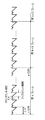
- FIG. 1 is a diagram showing a configuration example of the solid-state image sensor according to the first embodiment.
- FIG. 2 is an explanatory diagram showing an example of a multi-pixel one-cell structure in a Bayer array composed of pixels corresponding to RGB in the first embodiment.
- FIG. 3A is a diagram showing an example of a circuit configuration having a vertical 2-pixel 1-cell structure in FIG.
- FIG. 3B is a diagram showing an example of a circuit configuration having a vertical 4-pixel 1-cell structure in FIG.
- FIG. 4 is a diagram showing an example in which the solid-state image sensor according to the first embodiment is configured as a laminated back-illuminated image sensor.
- FIG. 1 is a diagram showing a configuration example of the solid-state image sensor according to the first embodiment.
- FIG. 2 is an explanatory diagram showing an example of a multi-pixel one-cell structure in a Bayer array composed of pixels corresponding to RGB in the first embodiment.
- FIG. 3A is a diagram showing an example of a circuit configuration
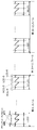
- FIG. 5A is a diagram showing an example of the pixel cross-sectional structure of the laminated back-illuminated image sensor of FIG. 4 according to the first embodiment.
- FIG. 5B is a diagram showing an example of the pixel cross-sectional structure of the laminated back-illuminated image sensor as the solid-state image sensor according to the second embodiment.
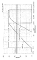
- FIG. 6A is a diagram showing an example of the potential change of the storage capacity element according to the exposure time.
- FIG. 6B is a diagram showing another example of the potential change of the storage capacitance element according to the exposure time.
- FIG. 7A is a diagram showing the potential change of the plug portion of the storage capacitance element according to the exposure time when the analog gain is 0 dB.
- FIG. 7B is a diagram showing the potential change of the plug portion of the storage capacitance element according to the exposure time when the analog gain is 6 dB.
- FIG. 7C is a diagram showing the potential change of the plug portion of the storage capacitance element according to the exposure time when the analog gain is 12 dB.
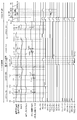
- FIG. 8 is a time chart of several frames showing an example of a signal reading operation associated with n exposure operations of the solid-state image sensor which is the basis of the first embodiment.
- FIG. 9 is a 1H (1 horizontal period) time chart showing an example of a signal reading operation associated with one exposure operation of the solid-state image sensor which is the basis of the first embodiment.
- FIG. 10 is a diagram showing a reading order of several frames in the first embodiment.
- FIG. 11 is a diagram showing the reading order of pixel signals in the CDS within the 1H period.
- FIG. 12 is a time chart showing an operation example of pixel readout accompanied by gain control according to the first embodiment.
- FIG. 13 is a diagram showing the relationship between the subject illuminance and the gain (SN ratio) according to the first embodiment.
- FIG. 14A is a diagram showing the potential at the main points of FIG.
- FIG. 14B is a diagram showing the potential at the main points of FIG.
- FIG. 14C is a diagram showing the potential at the main points of FIG.
- FIG. 15A is an explanatory diagram showing the concept of pixel mixing.
- FIG. 15B is a diagram for explaining each point of FIG. 15A.
- FIG. 15C is a diagram for explaining each point of FIG. 15A.
- FIG. 16 is an explanatory diagram of the scanning period of FIG. 15A.
- FIG. 17 is a diagram showing the timing of charge accumulation of the photodiode and the storage capacitance element.
- FIG. 18 is a diagram showing the timing of charge accumulation of the photodiode and the storage capacitance element.
- FIG. 19A is a diagram showing a configuration example of a signal processing unit that performs WDR synthesis using two frames.
- FIG. 19B is a diagram showing a configuration example of a signal processing unit that performs WDR synthesis using two frames.
- FIG. 20 is a diagram showing [1] charge accumulation level, [2] FD potential, [3] value after AD conversion, and [4] SN with respect to the product of illuminance and exposure time.
- FIG. 20 is a diagram showing [1] charge accumulation level, [2] FD potential, [3] value after AD conversion, and [4] SN with respect to the product of illuminance and exposure time.
- FIG. 21 is a diagram showing deterioration of SN due to the attenuation ratio of exposure (high illuminance).
- FIG. 22 is a diagram showing the signal charge amount and the FD potential of the first Read1 for reading the low-light frame and the second Read2 for reading the high-light frame.
- FIG. 23 is a diagram showing the effect of the present embodiment, that is, the effect of reducing the area of the storage capacitance element and expanding the dynamic range.
- FIG. 24A is a diagram showing a circuit configuration example of a vertical 2-pixel 1-cell structure according to the second embodiment.
- FIG. 24B is a diagram showing a circuit configuration example of a vertical 4-pixel 1-cell structure according to the second embodiment.
- FIG. 25 is a diagram showing the reading order of several frames in the second embodiment.
- FIG. 26 is a diagram showing the reading order of pixel signals in the CDS within the 1H period.
- FIG. 27 is a time chart showing an operation example of pixel readout accompanied by gain control according to the second embodiment.
- FIG. 28A is a diagram showing the potential at the main points of FIG. 27.
- FIG. 28B is a diagram (continued) showing the potential at the main points of FIG. 27.
- FIG. 28C is a diagram (continued) showing the potential at the main points of FIG. 27.
- FIG. 29A is an explanatory diagram showing the concept of pixel mixing.
- FIG. 29B is a diagram for explaining each point of FIG. 29A.
- FIG. 30 is an explanatory diagram of the scanning period of FIG. 29A.
- FIG. 31 is a diagram showing the timing of charge accumulation of the photodiode and the storage capacitance element.
- FIG. 32 is a diagram showing the timing of charge accumulation of the photodiode and the storage capacitance element.
- FIG. 33 is a diagram showing [1] charge accumulation level, [2] FD potential, [3] value after AD conversion, and [4] SN with respect to the product of illuminance and exposure time.
- FIG. 34 is a diagram showing the deterioration of SN due to the attenuation ratio of exposure (high illuminance).
- FIG. 35 is a diagram showing the signal charge amount and FD potential of the first Read1 for reading the low-light frame, the second Read2 for reading the medium-light frame, and the third Read3 for reading the high-light frame.
- FIG. 36 is a diagram showing the relationship between the subject illuminance and the gain (SN ratio) according to the second embodiment.
- FIG. 37 is a diagram showing the effect of the present embodiment, that is, the effect of reducing the area of the storage capacitance element and expanding the dynamic range.
- FIG. 38A is a diagram showing a circuit configuration example of a vertical 2-pixel 1-cell structure according to the third embodiment.
- FIG. 38B is a diagram showing a circuit configuration example of a vertical 4-pixel 1-cell structure according to the third embodiment.
- FIG. 39 is a diagram showing the reading order of pixel signals in the CDS within the 1H period according to the third embodiment.
- FIG. 40A is a time chart showing an operation example of pixel readout accompanied by gain control according to the third embodiment.
- FIG. 40A is a time chart showing an operation example of pixel readout accompanied by gain control according to the third embodiment.
- FIG. 40B is a time chart (continued) showing an operation example of pixel readout accompanied by gain control according to the third embodiment.
- FIG. 41A is an explanatory diagram showing the concept of pixel mixing.
- FIG. 41B is a diagram for explaining each point of FIG. 41A.
- FIG. 41C is a diagram for explaining each point of FIG. 41A.
- FIG. 42A is a diagram showing the potential at the main points of FIGS. 40A and 40B.
- 42B is a diagram (continued) showing the potential at the main points of FIGS. 40A and 40B.
- 42C is a diagram (continued) showing the potential at the main points of FIGS. 40A and 40B.
- 42D is a diagram (continued) showing the potential at the main points of FIGS.
- FIG. 40A and 40B. 42E is a diagram (continued) showing the potential at the main points of FIGS. 40A and 40B.
- FIG. 43 is an explanatory diagram of the scanning period of FIG. 41A.
- FIG. 44 is a diagram showing the timing of charge accumulation of the photodiode and the storage capacitance element.
- FIG. 45 is a diagram showing the timing of charge accumulation of the photodiode and the storage capacitance element.
- FIG. 46 is a diagram showing [1] charge accumulation level, [2] FD potential, [3] value after AD conversion, and [4] SN with respect to the product of illuminance and exposure time.
- FIG. 47 is a diagram showing deterioration of SN due to the attenuation ratio of exposure (high illuminance).
- FIG. 48 is a diagram showing the signal charge amount and the FD potential of the first Read1 for reading the low-light frame and the second Read2 for reading the high-light frame.
- FIG. 49 is a diagram showing the relationship between the subject illuminance and the gain (SN ratio) according to the third embodiment.
- FIG. 50 is a diagram showing the effect of the present embodiment, that is, the effect of reducing the area of the storage capacitance element and expanding the dynamic range.
- FIG. 51A is a diagram showing a circuit configuration example of a vertical 2-pixel 1-cell structure according to the fourth embodiment.
- FIG. 51B is a diagram showing a circuit configuration example of a vertical 4-pixel 1-cell structure according to the fourth embodiment.
- FIG. 52 is a diagram showing the reading order of several frames in the fourth embodiment.
- FIG. 51A is a diagram showing a circuit configuration example of a vertical 2-pixel 1-cell structure according to the fourth embodiment.
- FIG. 51B is a diagram showing a circuit configuration example of a vertical 4-pixel 1-cell structure according
- FIG. 53 is a diagram showing the reading order of pixel signals in the CDS within the 1H period.
- FIG. 54A is a time chart showing an operation example of pixel readout accompanied by gain control according to the fourth embodiment.
- FIG. 54B is a time chart (continued) showing an operation example of pixel readout accompanied by gain control according to the fourth embodiment.
- FIG. 55A is a diagram showing the potential at the main points of FIGS. 54A and 54B.
- FIG. 55B is a diagram (continued) showing the potential at the main points of FIGS. 54A and 54B.
- FIG. 55C is a diagram (continued) showing the potential at the main points of FIGS. 54A and 54B.
- FIG. 54A is a time chart showing an operation example of pixel readout accompanied by gain control according to the fourth embodiment.
- FIG. 55A is a diagram showing the potential at the main points of FIGS. 54A and 54B.
- FIG. 55B is a diagram (continue
- FIG. 55D is a diagram (continued) showing the potential at the key points of FIGS. 54A and 54B.
- FIG. 55E is a diagram (continued) showing the potential at the key points of FIGS. 54A and 54B.
- FIG. 56A is an explanatory diagram showing the concept of pixel mixing.
- FIG. 56B is a diagram for explaining each point of FIG. 56A.
- FIG. 56C is a diagram for explaining each point of FIG. 56A.
- FIG. 57 is an explanatory diagram of the scanning period of FIG. 56A.
- FIG. 58 is a diagram showing the timing of charge accumulation of the photodiode and the storage capacitance element.
- FIG. 59 is a diagram showing the timing of charge accumulation of the photodiode and the storage capacitance element.
- FIG. 60 is a diagram showing [1] charge accumulation level, [2] FD potential, [3] value after AD conversion, and [4] SN with respect to the product of illuminance and exposure time.
- FIG. 61 is a diagram showing deterioration of SN due to the attenuation ratio of exposure (high illuminance).
- FIG. 62 is a diagram showing the signal charge amount and FD potential of the first Read1 for reading the low-light frame, the second Read2 for reading the medium-light frame, and the third Read3 for reading the high-light frame. is there.
- FIG. 63 is a diagram showing the relationship between the subject illuminance and the gain (SN ratio) according to the fourth embodiment.
- FIG. 64 is a diagram showing the effect of the present embodiment, that is, the effect of reducing the area of the storage capacitance element and expanding the dynamic range.
- FIG. 65A is a diagram showing a circuit configuration example of a vertical 2-pixel 1-cell structure according to the fifth embodiment.
- FIG. 65B is a diagram showing a circuit configuration example of a vertical 4-pixel 1-cell structure according to the fifth embodiment.
- FIG. 66 is a diagram showing the reading order of several frames in the fifth embodiment.
- FIG. 67 is a diagram showing the reading order of pixel signals in the CDS within the 1H period.
- FIG. 68A is a time chart showing an operation example of pixel readout accompanied by gain control according to the fifth embodiment.
- FIG. 68B is a time chart (continued) showing an operation example of pixel readout accompanied by gain control according to the fifth embodiment.
- FIG. 69A is a diagram showing the potential at the main points of FIGS. 68A and 68B.
- FIG. 69B is a diagram (continued) showing the potential at the main points of FIGS. 68A and 68B.
- FIG. 69C is a diagram (continued) showing the potential at the main points of FIGS. 68A and 68B.
- FIG. 70A is an explanatory diagram showing the concept of pixel mixing.
- FIG. 70B is a diagram for explaining each point of FIG. 70A.
- FIG. 70C is a diagram for explaining each point of FIG. 70A.
- FIG. 70A is an explanatory diagram showing the concept of pixel mixing.
- FIG. 70B is a diagram for explaining each point of FIG. 70A.
- FIG. 70C is a diagram for explaining each point of FIG. 70A
- FIG. 71 is an explanatory diagram of the scanning period of FIG. 70A.
- FIG. 72 is a diagram showing the timing of charge accumulation of the photodiode and the storage capacitance element.
- FIG. 73 is a diagram showing the timing of charge accumulation of the photodiode and the storage capacitance element.
- FIG. 74 is a diagram showing [1] charge accumulation level, [2] FD potential, [3] value after AD conversion, and [4] SN with respect to the product of illuminance and exposure time.
- FIG. 75 is a diagram showing deterioration of SN due to the attenuation ratio of exposure (high illuminance).
- FIG. 76 is a diagram showing the signal charge amount and the FD potential of the first Read1 for reading the low-light frame and the second Read2 for reading the high-light frame.
- FIG. 77 is a diagram showing the relationship between the subject illuminance and the gain (SN ratio) according to the fifth embodiment.
- FIG. 78 is a diagram showing a configuration example of the image pickup apparatus according to the sixth embodiment.
- FIG. 79 is a diagram showing another configuration example of the imaging device according to the sixth embodiment.
- FIG. 80 is a diagram showing an example of mounting the imaging device according to the sixth embodiment in an automobile.
- FIG. 81 is a diagram showing an example of an imaging range in the mounting example of FIG. 80 according to the sixth embodiment.
- FIG. 82 is an explanatory diagram of the LED flicker.
- FIG. 82 is an explanatory diagram of the LED flicker.
- the horizontal axis in the figure indicates the frequency of the flicker, that is, the frequency in which the LED is turned on and off in one cycle.
- the vertical axis shows the flicker duty, that is, the ratio of lighting in the cycle of lighting and extinguishing.
- the flicker frequency of a traffic light is about 90 Hz
- the flicker frequency of a car headlight is about 1000 Hz.
- the first problem is the omission of LED light (light emission that repeats turning on and off, pulsed light) (problem 1).
- the cause is a mismatch between the exposure timing by the rolling shutter and the LED lighting timing, especially when the exposure time is short in the light (Cause 1).
- the second issue is pixel saturation (issue 2).
- the cause is that when the duty of the LED flicker is large or the exposure time is long, the pixels reach the saturation level and the white balance is lost (cause 2).
- the countermeasures for these (problem 1) and (problem 2) are to increase the saturation level of the pixels so that the saturation / sensitivity ratio is high and expand the dynamic range.
- an overflow element (OF1 to OF (m)) and a storage capacity element (C1 to C (m)) are set as one set, and an overflow element group composed of multiple stages (m ⁇ 2) is provided in series.
- the electric charge overflowing from the photodiode is received by the storage capacitance element via the overflow element. Further, the electric charge overflowing from the storage capacity element is received by the storage capacity element via the overflow element. Then, the signal charge accumulated in the storage capacitance element is redistributed and attenuated during the exposure period.
- the storage capacity element small with high-sensitivity pixels, in other words, increasing the saturation level without sacrificing sensitivity.
- the gain in the pixel is increased, and the noise generated in the pixel amplification transistor or the analog circuit is affected by the amount of light received.
- the voltage (pixel signal) may be increased. That is, for a dark subject, it is possible to output a high-quality image with a high SN (Signal to Noise ratio).
- high saturation pixels with a high saturation / sensitivity ratio are used to lower the intra-pixel gain, thereby expanding the dynamic range and enabling long-term exposure time. That is, for a bright subject, the gradation according to the subject is accurately reproduced to enable the output of an image without overexposure, and further, the flicker can be suppressed.
- the present inventors use highly saturated pixels with a high saturation / sensitivity ratio as a technique for expanding the dynamic range and suppressing flicker to improve the image quality in low illuminance and expand the dynamic range and flicker in high illuminance.
- a solid-state image sensor that achieves both suppression.
- Long exposure was for low illuminance with a long exposure time
- Middle exposure was for medium illuminance with a medium exposure time
- Short exposure was for high illuminance with a short exposure time.
- the exposure time is basically the same for all frames. That is, the terms Long, Middle, and Short do not imply different lengths of exposure time herein. Therefore, in this document, Long exposure is defined as low illuminance exposure, Middle exposure is defined as medium illuminance exposure, and Short exposure is defined as high illuminance exposure.
- the contact or plug part for connecting the wiring and the silicon substrate becomes a source of dark characteristics (dark current, noise, fixed roughness), it is necessary to take measures for the characteristics and reliability.
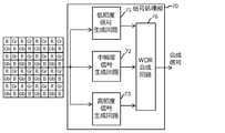
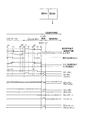
- FIG. 1 is a block diagram showing a configuration example of the solid-state image sensor 100 according to the first embodiment.
- the solid-state image sensor 100 shown in the figure includes a pixel array unit 10, a horizontal scanning circuit 12, a vertical scanning circuit 14, a plurality of vertical signal lines 19, a timing control unit 20, a column processing unit 26, a reference signal generation unit 27, and an output circuit. 28, and a signal processing unit 70. Further, the solid-state image sensor 100 includes an MCLK terminal that receives an input of a master clock signal from the outside, a DATA terminal for transmitting and receiving commands or data to and from the outside, a D1 terminal for transmitting video data to the outside, and the like. In addition to this, it is equipped with terminals to which the power supply voltage and ground voltage are supplied.
- the pixel array unit 10 has a plurality of pixel circuits 3 arranged in a matrix.
- the plurality of pixel circuits 3 are arranged in n rows and m columns in FIG.
- Each pixel circuit 3 includes a high-sensitivity pixel, a storage capacity element, and an overflow element.
- the overflow element is also called an overflow gate.
- the horizontal scanning circuit 12 outputs the AD-converted pixel signal to the horizontal signal line 18 by sequentially scanning the memories 256 in the plurality of column AD circuits 25. This scan may be in the same order as the column AD circuit 25.
- the vertical scanning circuit 14 scans a horizontal scanning line group (also referred to as a row control line group) 15 provided for each row of the pixel circuit 3 in the pixel array unit 10 in units of rows. As a result, the vertical scanning circuit 14 selects the pixel circuit 3 line by line, and simultaneously outputs pixel signals from the pixel circuit 3 belonging to the selected line to m vertical signal lines 19.
- the number of horizontal scanning line groups 15 is the same as the number of rows of the pixel circuit 3. In FIG. 1, n horizontal scanning line groups 15 (V1, V2, ..., Vn in FIG. 1) are provided.
- Each of the horizontal scanning line groups 15 includes a reset control line ⁇ RS, a transfer control line for accumulated charge ⁇ TGC1, ⁇ TGC2, ⁇ TGC3, a gain control line ⁇ GC1, ⁇ GC2, a selection control line ⁇ SEL, an overflow control line ⁇ OF1, ⁇ OF2, and ⁇ OF3.
- the vertical signal line 19 is provided for each column of the pixel circuit 3 in the pixel array unit 10, and propagates the pixel signal from the pixel circuit 3 belonging to the selected row to the column AD circuit 25.
- the plurality of vertical signal lines 19 are composed of m vertical signal lines H1 to Hm in FIG.
- the plurality of ADC input lines are composed of m lines of ADC input lines ADIN1 to ADINm in FIG.
- the timing control unit 20 controls the entire solid-state image sensor 100 by generating various control signal groups.
- the various control signal groups include control signal groups CN1, CN2, CN4, CN5, CN8, and counter clock signal CK0.
- the timing control unit 20 receives the master clock MCLK via the terminal, generates various internal clocks, and controls the horizontal scanning circuit 12 and the vertical scanning circuit 14.
- the column processing unit 26 includes a column AD circuit 25 provided for each column.
- Each column AD circuit 25 AD-converts the pixel signal from the vertical signal line 19.
- Each of the column AD circuits 25 includes a voltage comparator 252, a counter unit 254, and a memory 256.
- the voltage comparator 252 compares the analog pixel signal from the vertical signal line 19 with the reference signal RAMP including the lamp waveform (that is, the triangular wave) generated by the reference signal generation unit 27. For example, the former is more than the latter. When it becomes large, the output signal indicating the comparison result is inverted.
- the counter unit 254 counts the time from the start of the change of the triangular wave in the reference signal RAMP to the inversion of the output signal of the voltage comparator 252. Since the time until inversion is determined according to the value of the analog pixel signal, the count value becomes the value of the digitized pixel signal.
- the memory 256 holds the count value of the counter unit 254, that is, the digital pixel signal.
- the reference signal generation unit 27 generates a reference signal RAMP including a triangular wave, and outputs the reference signal RAMP to the positive input terminal of the voltage comparator 252 in each column AD circuit 25.
- the output circuit 28 outputs a digital pixel signal to the video data terminal D1.
- the signal processing unit 70 has a WDR synthesis circuit 76, and synthesizes a low-light signal, a medium-light signal, and a high-light signal. As a result, the signal processing unit 70 aims to achieve both expansion of the dynamic range and suppression of flicker.
- FIG. 2 is an explanatory diagram showing an example of a multi-pixel 1-cell structure in a Bayer array composed of pixels corresponding to RGB in the first embodiment.
- FIG. 3A is a diagram showing an example of a circuit configuration having a vertical 2-pixel 1-cell structure in FIG.
- FIG. 3B is a diagram showing an example of a circuit configuration having a vertical 4-pixel 1-cell structure in FIG.
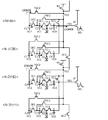
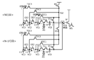
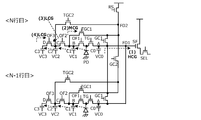
- FIG. 3A and 3B are diagrams showing a circuit example of the pixel circuit 3 according to the first embodiment.
- the pixel circuit 3 in the figure shows the photodiode PD, the transfer transistor TG, the overflow gate OF1, the storage capacitance element C1, the storage transfer transistor TGC1, the overflow gate OF2, the storage capacitance element C2, and the storage transfer. It includes a transistor TGC2, a stray diffusion layer FD1, a parasitic capacitance C0, a stray diffusion layer FD2, a reset transistor RS, a gain control transistor GC1, a gain control transistor GC2, an amplification transistor SF, and a selection transistor SEL.
- the horizontal scanning line group 15 includes a reset control line ⁇ RS, a read control line ⁇ TG, ⁇ TGC1, ⁇ TGC2, a gain control line ⁇ GC1, ⁇ GC2, a selection control line ⁇ SEL, an overflow control line ⁇ OF1, and an overflow control line ⁇ OF2.
- the photodiode PD is a photoelectric conversion element such as a photodiode, which performs photoelectric conversion with a predetermined sensitivity, that is, generates an electric charge according to the amount of received light.
- the photodiode PD is provided with a MIM capacity or a MOS capacity on the wiring layer on the side opposite to the light receiving side of the photodiode PD. This can be achieved by increasing the opening area of. It is also possible to provide a trench capacity in the cell.
- the solid-state image sensor 100 can also be configured as a laminated back-illuminated image sensor.
- FIG. 4 is a diagram showing an example in which the solid-state image sensor according to the first embodiment is configured as a laminated back-illuminated image sensor.
- a laminated BSI (Back Side Illumination) type CIS is used, a storage capacity element is mounted on the wiring layer side of the pixel chip (top chip), and the wiring layer side of the logic chip (bottom chip).
- the bonding is performed by Pixcel-to-Pixcel, but it is not necessary to expand the pixel area and the increase in the chip area can be suppressed.
- the capacitance C0 connected to the floating diffusion layer FD holds the signal charge (for example, an electron) transferred from the photodiode PD, converts the held signal charge into a voltage, and converts the converted voltage into the gate of the amplification transistor SF. Supply to.
- the actual capacitance of the stray diffusion layer FD is not only the capacitance of the stray diffusion layer FD itself, but also the gate capacitance of the amplification transistor SF, the gate-drain capacitance of the amplification transistor SF, and when the gain control transistor GC1 is on.
- the stray capacitance of the drain wiring of the gain control transistor GC1 is included.
- the transfer transistor TG is a switch transistor that turns on and off according to the read control signal ⁇ TG.
- the transfer transistor TG transfers the signal charge photoelectrically converted by the photodiode PD to the floating diffusion layer FD when the read control signal ⁇ TR is at a high level.
- the overflow gate OF1 is an overflow gate / switch transistor that turns on and off according to the read control signal ⁇ OF1. When the read control signal ⁇ OF1 is at a high level, the overflow gate OF1 transfers the signal charge photoelectrically converted by the photodiode PD to the storage capacitance element C1 via the overflow gate OF1.
- the signal charge photoelectrically converted by the photodiode PD overflows, it is transferred to the storage capacitance element C1 by adjusting the control voltage of the overflow gate OF1. Alternatively, it is transferred when the potential exceeds a preset value.
- the overflow gate OF2 can also be designed as an overflow gate / switch transistor capable of redistributing charges by turning on / off the read control signal ⁇ OF2.
- the overflow gate OF2 transfers the signal charge photoelectrically converted by the photodiode PD to the storage capacitance element C2 via the overflow gate OF2.
- the storage capacitance element C2 transfers the signal charge by adjusting the control voltage of the overflow gate OF2. Alternatively, transfer is performed when the potential exceeds a preset value.
- the charge of C2 when the charge is redistributed by turning on / off the read control signal ⁇ OF2 is attenuated 1 / M times.
- the attenuation ratio M is determined by (C1 + C2) / C2.
- the reset transistor RS is a switch transistor that turns on and off according to the reset control signal ⁇ RS.
- the reset transistor RS sets the power supply voltage applied to the drain as the reset level to the floating diffusion layer FD via the gain control transistor GC1. That is, the reset transistor RS resets the floating diffusion layer FD to the reset level when the reset control signal ⁇ RS is at a high level.
- the gain control transistor GC1 electrically disconnects or connects the floating diffusion layer FD1 and the floating diffusion layer FD2 according to the gain control signal ⁇ GC1. As a result, the signal charge in the floating diffusion layer FD1 is changed to a conversion gain that converts it into a voltage. That is, in the transfer of the signal charge from the photodiode PD to the floating diffusion layer FD1, if the gain control transistor GC1 is turned off, the conversion gain of the floating diffusion layer FD can be further increased.
- the gain control transistor GC2 electrically disconnects or connects the floating diffusion layer FD2 having a vertical 2-pixel 1-cell structure in response to the gain control signal ⁇ GC2. As a result, the signal charge in the floating diffusion layer FD2 is changed to a conversion gain that converts it into a voltage. That is, in the transfer of the signal charge from the photodiode PD to the floating diffusion layer FD2, if the gain control transistor GC2 is turned on, the conversion gain of the floating diffusion layer FD can be further lowered.
- the electric charge in the adjacent row that is, the transfer of the electric charge through the storage transfer transistor TGC1 and the storage transfer transistor TGC2 can be turned ON / OFF, and the charge can be redistributed.
- the amplification transistor SF forms a source follower together with the load current source 30 connected to the vertical signal line 19, and outputs the gate voltage, that is, the voltage of the stray diffusion layer FD to the vertical signal line 19 as an analog pixel signal.
- the selection transistor SEL is a switch transistor that turns on and off according to the selection control signal ⁇ SEL.
- the selection transistor SEL electrically connects the source of the amplification transistor SF and the vertical signal line 19 when the selection control signal ⁇ SEL is at a high level.
- FIG. 5A is a diagram showing an example of the pixel cross-sectional structure of the laminated back-illuminated image sensor of FIG. 4 in the first embodiment.
- FIG. 5B is a diagram showing an example of the pixel cross-sectional structure of the laminated back-illuminated image sensor as the solid-state image sensor according to the second embodiment described later.
- the wiring connected to the substrate at one end of the MIM capacity or MOS capacity is a poly plug using polysilicon wiring instead of metal wiring, damage to the connection portion is reduced and darkness characteristics ( Dark current, noise, fixed roughness) can be suppressed.
- the wiring connected to the substrate at one end of the gate wiring of the amplification transistor SF is a polysilicon plug (polysilicon contact (n)) using polysilicon wiring instead of metal wiring, damage to the connection portion is reduced and dark characteristics (darkness characteristics) Dark current, noise, fixed roughness) can be suppressed.
- the potentials (A, B, C) of the plug portion that stores the signal charges (negative charges) constituting the capacitive element increase in dark characteristics (dark current, noise, fixed roughness) when the potential with respect to GND is high. .. Therefore, the potential on the opposite side of the storage capacitance element (VC1, VC2, VC3) can be set to an intermediate potential between the GND and the pixel potential during exposure to improve the dark characteristics.
- TDDB Time Dependent Dilectric Breakdown
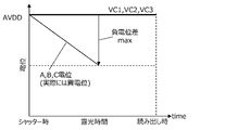
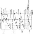
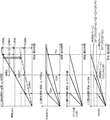
- FIG. 6A is a diagram showing an example of the potential change of the storage capacity element according to the exposure time.
- FIG. 6B is a diagram showing another example of the potential change of the storage capacitance element according to the exposure time.
- the horizontal axis shows the exposure time.
- the vertical axis shows the electric potential.
- FIG. 6B shows a case where only the negative side of the storage capacitance element is used.
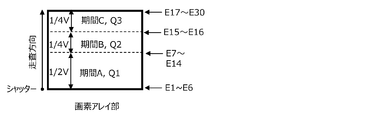
- the potentials of one of the storage capacitance elements VC1, VC2, and VC3 are the pixel potentials at the time of shuttering, and the potentials A, B, and C of the storage capacitance elements are also the pixel potentials at the time of shuttering.
- A-VC1, B-VC2, C-VC3) become negative and spread.
- the potential difference of the storage capacitance element can be used only on one side, the amplitude is narrow and the dynamic range is narrow. Moreover, since the A, B, and C potentials are high, the dark current tends to be bad.
- FIG. 6A shows the case where the positive side and the negative side of the storage capacitance element are used.
- the potentials of one of the storage capacity elements VC1, VC2, and VC3 are intermediate potentials at the time of shuttering, and the potentials of A, B, and C of the storage capacity elements are pixel potentials at the time of shuttering.
- the potential difference (A-VC1, B-VC2, C-VC3) is a positive potential at first, and gradually becomes a negative potential and increases.
- the amplitude and dynamic range can be expanded twice as much as in the case of FIG. 6B. Moreover, since the A, B, and C potentials are low, the dark current becomes good.
- the potentials of one of the storage capacitance elements VC1, VC2, and VC3 can be further lowered, so that the dark characteristics of the potentials (A, B, C) of the plug portion are deteriorated. Can be suppressed.
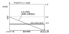
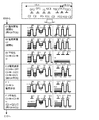
- 7A, 7B, and 7C are diagrams showing the potential change of the plug portion of the storage capacitance element according to the exposure time when the analog gains are 0 dB, 6 dB, and 12 dB, respectively.
- the potential of the plug portion of the storage capacitance element may also be set to 1 / 2V: 1 / 4V: 1 / 8V as shown in the figure by providing gain interlocking.
- the potentials of VC1, VC2, and VC3 at the time of shuttering are 1 / 2V, and by setting the A, B, and C potentials to 0 dB (reference ratio), the A, B, and C potentials are lowered, so that the dark current is improved. (Compared to FIG. 7B).
- the potentials of VC1, VC2, and VC3 at the time of shuttering are 1 / 4V, and by setting the A, B, and C potentials to -6 dB (reference ratio), the A, B, and C potentials are lowered, so that the dark current is good. To become.
- the potentials of VC1, VC2, and VC3 at the time of shuttering are 1 / 8V, and by setting the A, B, and C potentials to -12 dB (reference ratio), the A, B, and C potentials are lowered, so that the dark current is good. To become.
- FIG. 8 is a time chart of several frames showing an example of a signal reading operation accompanying n exposure operations of the solid-state image sensor 100 which is the basis of the first embodiment.
- FIG. 9 is a 1H (1 horizontal period) time chart showing an example of a signal reading operation associated with one exposure operation of the solid-state image sensor 100 which is the basis of the first embodiment.
- the reference signal RAMP becomes a triangular wave in each of the down count period (t10 to t14) and the upcount period (t20 to t24).
- the down count period is a period for AD conversion of the level of the reset component Vrst in the analog pixel signal output from the amplification transistor SF.
- the counter unit 254 downcounts the time from the start of the downcount period (start of change of the triangular wave) to the inversion of the output of the voltage comparator 252. This count value is the AD conversion result itself of the reset component Vrst of the analog pixel signal.
- the upcount period is a period for AD conversion of the level of the data component (signal component Vsig + reset component Vrst) of the analog pixel signal output from the amplification transistor SF.
- the counter unit upcounts the time from the start of the upcount period (start of change of the triangular wave) to the inversion of the output of the voltage comparator 252. This upcount converts the data component (Vsig + Vrst) of the analog pixel signal into a digital value.
- the count value at the end of the upcount period is CDS (Correlated Double Sample: Correlation Double Detection) in which the reset component is subtracted from the data component. Represents the result of. That is, the count value at the end of the up-count period is the digital value itself representing the signal component Vsig.
- CDS Correlated Double Sample: Correlation Double Detection
- FIG. 10 shows the reading order of several frames in the first embodiment.
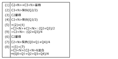
- FIG. 11 shows the CDS order of 1H, which is HCG (R: reset component) ⁇ HCG (S: signal component) ⁇ LCG (S: signal component) ⁇ LCG (R: reset component).
- FIG. 12 is a modification of the basic FIG. 9 in this CDS order.
- the pixel reset noise is canceled in the transition from HCG (R: reset component) to HCG (S: signal component).
- the DC offset reset coupling
- the pixel reset noise cannot be canceled and remains as kTC noise. Will be done.
- the kTC noise in this Short exposure appears on the low signal side.
- the kTC noise is represented by ⁇ (kTC) in terms of the amount of electric charge. This noise must be set to be well below the signal level.
- ⁇ kTC
- the latter SN needs to be sufficiently better than the former SN.
- FIG. 12 is a time chart showing an operation example of pixel readout accompanied by gain control according to the first embodiment.
- T * (* is a number) in FIG. 12 indicates the event No. in FIG. E * indicates the event numbers of FIGS. 14A, 14B, and 14C.
- timing is not limited to FIG. 12 as long as the same effect as that of the present embodiment can be obtained.
- the gain for converting the signal charge in the floating diffusion layer FD1 into a voltage can be switched between a high gain and a low gain according to the on and off of the gain control transistor GC1.
- the period from HCG (R: reset component) to HCG (S: signal component) shows the operation of reading the signal charge from the photodiode PD to the floating diffusion layer FD1 in a state where the conversion gain of the floating diffusion layer FD1 is high.
- LCG (S: signal component) ⁇ LCG (R: reset component) is an operation of reading a signal charge from the storage capacitance element C1 and the storage capacitance element C2 to the floating diffusion layer FD2 in a state where the conversion gain of the floating diffusion layer FD2 is low. Is shown.
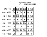
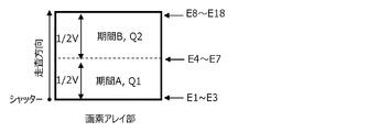
- the gain control transistor GC2 is mixed / separated in order to redistribute the pixel signal in the ⁇ N> row and the pixel signal in the ⁇ N-1> row (detailed description of the potential diagram will be described later). ..
- FIG. 15A is an explanatory diagram showing the concept of pixel mixing.
- FIG. 15B is a diagram for explaining each point of FIG. 15A.
- FIG. 15C is a diagram for explaining each point of FIG. 15A.
- FIG. 16 is an explanatory diagram of the scanning period of FIG. 15A. A detailed description of the potential diagram will be described below.
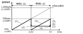
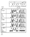
- the electric charge overflowing from the photodiode PD is accumulated only in the storage capacitance element C1 ⁇ N> ((1) in FIGS. 15A to 15C), and the stored charge increases as the exposure time increases. If the capacitance element that stores the electric charge is insufficient, it cannot receive 100 klux, and the dynamic range becomes insufficient.
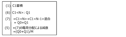
- the charge amount of C1 ⁇ N> becomes Q1 in the 1 / 2V period (1/2 vertical synchronization period) corresponding to half of the 1V period (1 vertical synchronization period), and becomes C2 ⁇ N>.
- the charge is redistributed and the charge becomes Q1 / M ((2) in the figure), and the charge is retained until the end period of the 1V period. After that, the unnecessary charge of C1 ⁇ N> is discharged.
- the damping ratio M is determined by the capacitance ratio (C1 + C2) / C2.
- the signal charge of (Q0 + Q1 + Q2) / M is obtained by reading the charge Q1 / M of C2 ⁇ N> and the charge (Q0 + Q2) / M of C2 ⁇ N-1> and mixing them by FD. ((5) in the figure).
- the feature of this embodiment is that the capacitance area is reduced by driving the storage capacitance element to use the capacitance of the adjacent row from which the electric charge has already been discharged.
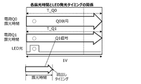
- LED light may be missed if the exposure is intermittent such as a chopper during the 1V exposure period, but the feature of the exposure method of the present embodiment is continuous exposure (PD and accumulation). Since it is a capacitive element), it can be achieved by reliably capturing the LED light.
- the photodiode PD continues to be exposed for a 1V period (1 vertical synchronization period), and the amount of charge is Q0.
- the storage capacitance element C1 ⁇ N> that receives the electric charge overflowing from the photodiode PD becomes a Q1 signal from 0 to 1 / 2V period, and becomes a Q2 signal from 1/2 to 1V period. Further, since the exposure is completely performed during the 1V period, it is possible to capture the LED light.
- the transition from 0 to 1 / 2V to 1/2 to 1V there is a possibility that a non-exposure period occurs at a level of several H, which is a level that does not affect the image quality of the LED light.
- the feature of this embodiment is that the two frames of Long and Short that synthesize WDR are exposed at exactly the same timing, and since the same pixels are used, false color, coloring, and blurring do not occur. There is.
- FIGS. 19A and 20 show an outline of the WDR synthesis method.
- the signal processing unit 70 of FIG. 19A includes a low-light signal generation circuit 71, a high-light signal generation circuit 73, and a WDR synthesis circuit 76.
- FIG. 19A is a diagram showing a configuration example of a signal processing unit that performs WDR synthesis using two frames.
- the WDR is synthesized with the Long exposure (low illuminance) as the signal charge of Q0 and the Short exposure (high illuminance) as the signal charge of (Q0 + Q1 + Q2) / M.
- the horizontal axes of [1], [2], [3], and [4] in FIG. 20 indicate the product of illuminance and exposure time, illuminance for a certain period of time, or exposure time at a constant illuminance.
- [1] indicates the charge accumulation level.
- [2] indicates the FD potential.
- [3] shows the value after AD conversion.
- [4] indicates SN.
- FIG. 21 shows the deterioration of SN due to the attenuation ratio M of short exposure (high illuminance). Since the SN is determined by the shot noise, for example, if the attenuation ratio M is doubled, the SN at the boundary will decrease by 3 dB.
- the capacitance ratio of the storage capacitance element (C1) and the storage capacitance element (C2) can be set by an arbitrary attenuation ratio M, but the deterioration of SN at the boundary at the time of synthesis after WDR is an index.
- FIG. 22 is a diagram showing the signal charge amount and the FD potential of the first Read1 for reading the low-light frame and the second Read2 for reading the high-light frame.
- FIG. 13 is a diagram showing the relationship between the subject illuminance and the gain (SN ratio) according to the first embodiment.
- the first Read1 is actually synthesized as a WDR Long frame (low-light frame)
- the second Read2 is actually synthesized as a WDR Short frame (high-light frame).
- the SN of the connecting portion of the frame is 26 dB or more
- the dynamic range is 120 dB or more.
- the dynamic range is extended from very dark illuminance (0.1 Lux) to very bright illuminance (100,000 Lux: equivalent to sunlight).
- the details of the WDR synthesis circuit 76 constituting the signal processing unit 70 are shown in FIG. 19A.
- the pixel signal of the first low-light frame (Long exposure) and the pixel signal of the second high-light frame (Short exposure) are combined.
- WDR function wide dynamic range function
- the pixel signal (Long exposure) of the first low-light frame is set to have a high intra-pixel gain
- the pixel signal (Short exposure) of the second high-light frame is set to have a low intra-pixel gain to improve noise and increase in low light. It is also possible to expand the dynamic range with illuminance.
- FIG. 23 shows the effect of this embodiment, that is, the effect of reducing the area of the storage capacitance element and expanding the dynamic range.
- the dynamic range can be expanded in a state where the storage capacitance element is reduced, and the received signal is not missed at all even for the high-luminance LED light.
- the case No. It is based on 1.
- the notation of "equivalent” in the figure is the case No. of (* 1).
- Case No. (* 2) It means that they are equivalent to each other.
- the FD1 is reset, and the charge of the PD section is discharged by turning on the reset transistor RS ⁇ N>, the transfer transistor TG ⁇ N>, and the gain control transistor GC1 ⁇ N>.
- the exposure starts in the period A, and the reset transistor RS ⁇ N>, the transfer transistor TG ⁇ N>, and the gain control transistor GC1 ⁇ N> are turned off.
- E3 the charge is accumulated in the period A, the signal charge Q0 is accumulated in the photodiode PD, and the overflowed charge is accumulated as Q1 in the storage capacitance element C1 ⁇ N> via the overflow gate OF1 ⁇ N>.
- E7 is the start of exposure in period B, and turns off the storage transfer transistor TGC1 ⁇ N> and the reset transistor RS ⁇ N>.
- E8 is the charge accumulation in the period B, the signal charge Q0 is accumulated in the photodiode PD, and the overflowed charge is accumulated in the storage capacitance element C1 ⁇ N> via the overflow gate OF1 ⁇ N>.
- E9 is a reset of the FD1 ⁇ N>, and the charge of the FD1 portion is discharged by turning on the reset transistor RS ⁇ N> and the gain control transistor GC1 ⁇ N>.
- E10 is a reset of HCG, and the reset transistor RS ⁇ N> and the gain control transistor GC1 ⁇ N> are turned off to enter the HCG state.
- E11 transfers the charge Q0 of the photodiode PD to the FD1 section by turning on the transfer transistor TG ⁇ N>.
- E12 reads out the charge Q0 of the photodiode PD accumulated in the FD1 portion by turning off the transfer transistor TG ⁇ N> (HCG signal).
- the charge Q2 of the storage transfer transistor TGC1 ⁇ N> is averaged and redistributed to Q0 of the FD1 part. Therefore, the gain control transistor GC2 ⁇ N>, the storage transfer transistor TGC1 ⁇ N>, and the storage transfer transistor TGC2 ⁇ N-1> are turned on to average the charges of Q0 and Q2.
- the E14 turns off the storage transfer transistor TGC1 ⁇ N> and the storage transfer transistor TGC2 ⁇ N-1>, and redistributes the charges of Q0 and Q2.
- the attenuation ratio M becomes (C1 ⁇ N> + C2 ⁇ N-1>) / C2 ⁇ N-1>, and the charge amount of C2 ⁇ N-1> becomes (Q0 + Q2) / M. ..
- E16 by turning on the storage transfer transistors TGC2 ⁇ N> and TGC2 ⁇ N-1>, the charge amount Q1 / M of C2 ⁇ N> and the charge amount (Q0 + Q2) / M of C2 ⁇ N-1> are set. When mixed, the total charge becomes (Q0 + Q1 + Q2) / M (LCG signal).
- the FD2 signal is read out.
- the problem with the overflow of electric charge overflowing from the photodiode PD is color mixing and linearity deviation due to leakage to other elements. Therefore, the height of the potential barrier at each overflow requires the following conditions. That is, the electric charge overflowing from the photodiode PD flows in the order of overflow gate OF1, OF2 ⁇ transfer transistor TG, storage transfer transistor TGC1, TGC2 ⁇ separation layer.
- the voltage of the overflow gate manufacturing variations occur and the saturation level tends to vary. Therefore, in particular, it is desirable that the voltages of the overflow gate OF1 and the overflow gate OF2 are controlled by trimming or the like before shipment to suppress saturation variation.
- Emodiment 2 The solid-state image sensor 100 according to the second embodiment will be described from the viewpoint of the difference from the first embodiment.
- the number of controls of the horizontal scanning line group 15 is different, but other than that, the configuration is the same.
- FIG. 2 shows a Bayer configuration composed of RGB
- FIG. 24A is a circuit configuration of the vertical 2 pixels and 1 cell
- FIG. 24B is a circuit configuration of the vertical 4 pixels and 1 cell.
- the control lines are all the same.
- 24A and 24B are diagrams showing a circuit example of the pixel circuit 3 according to the second embodiment.
- an overflow gate OF2 a storage capacity element C2, a storage transfer transistor TGC3, and a charge of the storage capacity element C3 are provided.
- the horizontal scanning line group 15 includes a read control line ⁇ TGC3 and an overflow control line ⁇ OF2.
- the overflow gate OF1 is an overflow gate / switch transistor that turns on and off according to the read control signal ⁇ OF1. When the read control signal ⁇ OF1 is at a high level, the overflow gate OF1 transfers the signal charge photoelectrically converted by the photodiode PD to the storage capacitance element C1 via the overflow gate OF1.
- the storage capacitance element C1 can be poured by adjusting the control voltage of the overflow gate OF1. Alternatively, transfer is performed when the potential exceeds a preset value.
- the overflow gate OF2 is an overflow gate / switch transistor that turns on and off according to the read control signal ⁇ OF2. When the read control signal ⁇ OF2 is at a high level, the overflow gate OF2 transfers the signal charge photoelectrically converted by the photodiode PD to the storage capacitance element C2 via the overflow gate OF2.
- the storage capacitance element C2 can be poured by adjusting the control voltage of the overflow gate OF2. Alternatively, it is poured when the potential exceeds a preset value.
- the overflow gate OF2 can also be designed as an overflow gate / switch transistor capable of redistributing charges by turning on / off the read control signal ⁇ OF2.
- the overflow gate OF2 transfers the signal charge photoelectrically converted by the photodiode PD to the storage capacitance element C2 via the overflow gate OF2.
- the storage capacitance element C3 transfers the signal charge by adjusting the control voltage of the overflow gate OF2. Alternatively, it is transferred when the potential exceeds a preset value.
- the overflow gate OF3 is an overflow gate / switch transistor that turns on and off according to the read control signal ⁇ OF3.
- the overflow gate OF3 transfers the signal charge photoelectrically converted by the photodiode PD to the storage capacitance element C3 via the overflow gate OF3.
- the attenuation ratio M when the charge is redistributed by turning on / off the read control signal ⁇ OF3 is determined by (C1 + C2) / C2.
- the gain control transistor GC2 electrically disconnects or connects the floating diffusion layer FD2 having a vertical 2-pixel 1-cell structure in response to the gain control signal ⁇ GC2. As a result, the signal charge in the floating diffusion layer FD2 is changed to a conversion gain that converts it into a voltage. That is, in the transfer of the signal charge from the photodiode PD to the floating diffusion layer FD2, if the gain control transistor GC2 is turned on, the conversion gain of the floating diffusion layer FD can be further lowered.
- the electric charge in the adjacent row that is, the transfer of the electric charge through the storage transfer transistor TGC1 and the storage transfer transistor TGC3 can be turned ON / OFF, and the charge can be redistributed.
- FIG. 25 shows the reading order of several frames in the second embodiment.
- FIG. 26 shows the CDS order of 1H, HCG (R: reset component) ⁇ HCG (S: signal component) ⁇ MCG (S: signal component) ⁇ LCG (S: signal component) ⁇ LCG (R: reset component) ⁇ It becomes MCG (R: reset component).
- FIG. 27 is a modification of the basic FIG. 9 in this CDS order. The pixel reset noise is canceled in the transition from HCG (R: reset component) to HCG (S: signal component).
- the kTC noise in this Short exposure appears on the low signal side.
- the kTC noise is represented by ⁇ (kTC) in terms of the amount of electric charge. It must be set to be sufficiently lower than the signal level. As described above, at the boundary between Short exposure (high illuminance) and Long exposure (low illuminance), the latter SN needs to be sufficiently better than the former SN.
- FIG. 27 is a time chart in which the main part is enlarged at 1 V (1 vertical synchronization period) showing an operation example of pixel readout accompanied by gain control according to the second embodiment.
- T * in FIG. 27 indicates the event No. in FIG. E * indicates the event numbers of FIGS. 28A, 28B, and 28C.
- timing is not limited to FIG. 27 as long as the same effect as that of the present embodiment can be obtained.
- the gain GC1 that converts the signal charge in the floating diffusion layer FD1 into a voltage can be switched between a high gain and a low gain according to the on and off of the gain control transistor GC1.
- the period from HCG (R: reset component) to HCG (S: signal component) shows the operation of reading the signal charge from the photodiode PD to the floating diffusion layer FD1 in a state where the conversion gain of the floating diffusion layer FD1 is high.
- MCG (S: signal component) ⁇ LCG (S: signal component) ⁇ LCG (R: reset component) ⁇ MCG (R: reset component) is the storage capacitance element C1 in a state where the conversion gain of the floating diffusion layer FD2 is low.
- the operation of reading the signal charge from the storage capacitance element C2 to the floating diffusion layer FD2 is shown.
- the gain control transistor GC2 is mixed / separated in order to redistribute the charge of the pixel signal in the ⁇ N> row and the pixel signal in the ⁇ N-1> row. (Detailed explanation of the potential diagram will be described below).
- FIG. 29A, 29B, and 30 show the concept of pixel mixing.
- FIG. 29A is an explanatory diagram showing the concept of pixel mixing.
- FIG. 29B is a diagram for explaining each point of FIG. 29A.
- FIG. 30 is an explanatory diagram of the scanning period of FIG. 29A. A detailed description of the potential diagram will be described below.
- the electric charge overflowing from the photodiode PD is accumulated at C2 ⁇ N>, and the electric charge of the accumulator element C2 increases as the exposure time increases ((1) in FIG. 29A). If the capacitance element that stores the electric charge is insufficient, it cannot receive 100 klux, and the dynamic range becomes insufficient.
- the charge amount of C1 ⁇ N> is Q1 in the 1 / 2V period corresponding to half of the 1V (1 vertical synchronization period) period. Then, the charge amount Q2 of C2 ⁇ N> is redistributed with C3 ⁇ N>, and the charge amount of C3 ⁇ N> becomes Q2 / M ((2) in the figure) and is held until the end period of 1V. deep. After that, the unnecessary charge of C2 ⁇ N> is discharged.
- the feature of this embodiment is that the capacitance area is reduced by driving the storage capacitance element to use the capacitance of the adjacent row from which the electric charge has already been discharged.
- the feature of the exposure method of the present embodiment is that during the exposure period of 1V period (1 vertical synchronization period), if the exposure is intermittent such as a chopper, LED light may be missed, but continuous exposure (PD and Since it is a storage capacity element), it can be achieved by reliably capturing LED light.
- FIGS. 31 and 32 show the timing of charge accumulation of the photodiode PD, the storage capacity element C1, and the storage capacity element C2.
- the photodiode PD continues to be exposed for a 1V period (1 vertical synchronization period), and the amount of charge is Q0.
- the storage capacitance element C1 ⁇ N> that receives the electric charge overflowing from the photodiode PD continues to be exposed for a 1V period (1 vertical synchronization period), and the amount of electric charge is Q1.
- the storage capacity element C2 ⁇ N> that receives the electric charge overflowing from the storage capacity element C1 ⁇ N> becomes a Q2 signal from 0 to 1 / 2V period and becomes a Q3 signal from 1/2 to 1V period.
- the feature of this embodiment is that the three frames of Long, Middle, and Short that synthesize WDR are exposed at exactly the same timing, and the same pixels are used completely, so that false color, coloring, and blurring occur. It is to stop.
- the signal processing unit 70 of FIG. 19B includes a low-light signal generation circuit 71, a medium-light signal generation circuit 72, a high-light signal generation circuit 73, and a WDR synthesis circuit 76.
- WDR WDR is synthesized as Q0 signal charge for Long exposure (low illuminance), Q0 + Q1 signal charge for Middle exposure (medium illuminance), and (Q0 + Q1 + Q2 + Q3) / M signal charge for Short exposure (high illuminance).
- FIGS. 33 [1] [2] [3] [4] indicate the product of illuminance and exposure time, illuminance for a certain period of time, or exposure time at a constant illuminance.
- [1] indicates the charge accumulation level.
- [2] indicates the FD potential.
- [3] shows the value after AD conversion.
- [4] indicates SN.
- FIG. 34 shows the deterioration of SN due to the attenuation ratio M of short exposure (high illuminance). Since the SN is determined by the shot noise, for example, if the attenuation ratio M is doubled, the SN at the boundary will decrease by 3 dB.
- the capacitance ratio of the storage capacitance element (C1) and the storage capacitance element (C2) can be set by an arbitrary attenuation ratio M, but the deterioration of SN at the boundary at the time of synthesis after WDR is an index.
- the SN of the connecting portion is improved as compared with the first embodiment.
- FIG. 35 is a diagram showing the signal charge amount and FD potential of the first Read1 for reading the low-light frame, the second Read2 for reading the medium-light frame, and the third Read3 for reading the high-light frame. is there.
- FIG. 36 is a diagram showing the relationship between the subject illuminance and the gain (SN ratio) according to the second embodiment.
- the first Read1 is actually a WDR Long frame (low-light frame)
- the second Read2 is a WDR Middle frame (medium-light frame)
- the third Read3 is a WDR Short frame (high-light frame). It is synthesized as.
- the SN of the connecting portion of the frame is 26 dB or more, and the dynamic range is 120 dB or more.
- the details of the WDR synthesis circuit 76 constituting the signal processing unit 70 are shown in FIG. 19B.
- the pixel signal (Long) of the first low-light frame, the pixel signal (Middle) of the second medium-light frame, and the pixel signal (Short) of the third high-light frame are combined.
- WDR function wide dynamic range function
- the pixel signal (Long) of the first low-illumination frame is set to have a high intra-pixel gain, and the pixel signal (Middle) of the second medium-illumination frame and the pixel signal (Short) of the third high-illumination frame are gained within the pixel. Is set low to improve noise in low light and expand the dynamic range in high light.
- FIG. 37 shows the effect of this embodiment, that is, the effect of reducing the area of the storage capacitance element and expanding the dynamic range.
- the dynamic range can be expanded in a state where the storage capacitance element is reduced, and the received signal is not missed at all even for the high-luminance LED light.
- the case No. It is based on 1.
- E1 is a reset of the FD1 and discharges the electric charge of the PD section by turning on the reset transistor RS ⁇ N>, the transfer transistor TG ⁇ N>, and the gain control transistor GC1 ⁇ N>.
- E2 is the start of exposure in the period A, and turns off the reset transistor RS ⁇ N>, the transfer transistor TG ⁇ N>, and the gain control transistor GC1 ⁇ N>.
- E3 is the charge accumulation in the period A, the signal charge Q0 is accumulated in the photodiode PD, the accumulation Q1 is further accumulated in the storage capacitance element C1 ⁇ N>, and the overflowed charge is accumulated through the overflow gate OF2. It is stored in the storage capacity element C2 ⁇ N>.
- E4 the charge Q2 accumulated in C2 ⁇ N> is first averaged in order to redistribute the charge with C3 ⁇ N>. Turn on the overflow gate OF3 ⁇ N>.
- E7 is the start of exposure in period B, and turns off the storage transfer transistor TGC2 ⁇ N> and the reset transistor RS.
- E8 is the charge accumulation in the period B, the signal charge Q0 is accumulated in the photodiode PD, Q1 is accumulated in the storage capacitance element C1 ⁇ N>, and the overflowed charge is stored capacity via the overflow gate OF2.
- Q3 is accumulated in the element C2 ⁇ N>.
- E9 is a reset of the FD1 and discharges the electric charge of the FD1 part by turning on the reset transistor RS ⁇ N> and the gain control transistor GC1 ⁇ N>.
- E10 is a reset of HCG, and the reset transistor RS ⁇ N> and the gain control transistor GC1 ⁇ N> are turned off to enter the HCG state.
- E11 transfers the electric charge of the photodiode PD to the FD1 unit by turning on the transfer transistor TG ⁇ N>.
- E12 reads out the charge Q0 of the photodiode PD accumulated in the FD1 portion by turning off the transfer transistor TG ⁇ N> (HCG signal).
- E13 reads the charge Q1 of the storage capacitance element C1 ⁇ N> into Q0 of the FD1 unit, averages it, and redistributes the charge.
- the signal for MCG is read out as Q0 + Q1 (MCG signal).
- the E15 turns on the above Q0 and Q1, the storage transfer transistors TGC2 ⁇ N> and TGC3 ⁇ N-1>, and sets the charges of Q0 + Q1 and C2 ⁇ N> to zero and the charges of C3 ⁇ N-1> to zero. Average.
- the storage transfer transistors TGC2 ⁇ N> and TGC3 ⁇ N-1> are turned off to redistribute the charges.
- the charge of C3 ⁇ N-1> is (Q3 + Q0 + Q1) / M.
- the charge amount Q2 / M of the storage capacitance element C3 ⁇ N> and the charge amount (Q0 + Q1 + Q3) / M of C3 ⁇ N-1> are mixed, and the total charge becomes (Q0 + Q1 + Q2 + Q3) / M.
- the attenuation ratio M (C2 ⁇ N> + C3 ⁇ N-1>) / C3 ⁇ N-1>.
- the problem with the overflow of electric charge overflowing from the photodiode PD is color mixing and linearity deviation due to leakage to other elements. Therefore, the height of the potential barrier at each overflow needs to be as follows. That is, the electric charge overflowing from the photodiode PD flows in the order of overflow gate OF1, 2 ⁇ transfer transistor TG, storage transfer transistor TGC1, 2 ⁇ separation layer.
- the voltage of the overflow gate manufacturing variations occur and the saturation level tends to vary. Therefore, in particular, it is desirable that the voltages of the overflow gate OF1 and the overflow gate OF2 be trimmed before shipment to suppress saturation variation.
- the solid-state image sensor 100 according to the third embodiment will be described from the viewpoint of the difference from the first embodiment.
- the number of controls of the horizontal scanning line group 15 is different, but other than that, the configuration is the same.
- FIG. 2 shows a Bayer configuration composed of RGB
- FIG. 38A is a circuit configuration of the vertical 2 pixels and 1 cell
- FIG. 38B is a circuit configuration of the vertical 4 pixels and 1 cell.
- the control lines are all the same.
- 38A and 38B have a configuration in which the storage capacitance element C2 is provided but the storage transfer transistor TGC2 is not provided in the third embodiment.
- the overflow gate OF2 has a device structure in which electric charges flow in both directions, and the electric charge of the storage capacitance element C2 is obtained by turning on the overflow gate OF2 and the storage transfer transistor TGC1. , The same effect can be obtained.
- the read control line ⁇ TGC2 is omitted.
- the overflow gate OF1 is an overflow gate / switch transistor that turns on and off according to the read control signal ⁇ OF1. When the read control signal ⁇ OF1 is at a high level, the overflow gate OF1 transfers the signal charge photoelectrically converted by the photodiode PD to the storage capacitance element C1 via the overflow gate OF1.
- the storage capacitance element C1 is transferred by adjusting the control voltage of the overflow gate OF1. Alternatively, it is transferred when the potential exceeds a preset value.
- the overflow gate OF2 is an overflow gate / switch transistor that turns on and off according to the read control signal ⁇ OF2. When the read control signal ⁇ OF2 is at a high level, the overflow gate OF2 transfers the signal charge photoelectrically converted by the photodiode PD to the storage capacitance element C2 via the overflow gate OF2.
- the storage capacitance element C2 transfers by adjusting the preset control voltage of the overflow gate OF2.
- the charge can be redistributed by turning the control voltage of the overflow gate OF2 ON / OFF.
- the storage capacity element C1 ⁇ N-1> in which the charge has already been discharged redistributes the signal charge photoelectrically converted by the storage capacity element C1 ⁇ N> by turning on / off the control voltage of the gain control transistor GC2. Can be done.
- the attenuation ratio M at this time is (C1 ⁇ N> + C1 ⁇ N-1>) / C1 ⁇ N>.
- FIG. 39 is a diagram showing the reading order of pixel signals in the CDS within the 1H period according to the third embodiment.
- FIG. 39 shows the CDS order of 1H, which is HCG (R: reset component) ⁇ HCG (S: signal component) ⁇ LCG (S: signal component) ⁇ LCG (R: reset component).
- 40A and 40B are the basics of FIG. 9 modified to this CDS order.
- the pixel reset noise is canceled in the transition from HCG (R: reset component) to HCG (S: signal component).
- the DC offset reset coupling
- the pixel reset noise cannot be canceled and remains as kTC noise. Will be done.
- the kTC noise in this Short exposure appears on the low signal side.
- the kTC noise is represented by ⁇ (kTC) in terms of the amount of electric charge. It must be set to be sufficiently lower than the signal level. As described above, at the boundary between Short exposure (high illuminance) and Long exposure (low illuminance), the latter SN needs to be sufficiently better than the former SN.
- FIGS. 40A and 40B are time charts in which the main part is enlarged in a 1V period (1 vertical synchronization period) showing an operation example of pixel readout accompanied by gain control according to the third embodiment.
- T * in FIGS. 40A and 40B indicates the event No. in FIG. E * indicates the event numbers of FIGS. 42A, 42B, and 42C.
- timing is not limited to FIGS. 40A and 40B as long as the same effect as that of the present embodiment can be obtained.
- the gain GC1 that converts the signal charge in the floating diffusion layer FD1 into a voltage can be switched between a high gain and a low gain according to the on and off of the gain control transistor GC1.
- the period from HCG (R: reset component) to HCG (S: signal component) shows the operation of reading the signal charge from the photodiode PD to the floating diffusion layer FD1 in a state where the conversion gain of the floating diffusion layer FD1 is high.
- LCG (S: signal component) ⁇ LCG (R: reset component) is an operation of reading a signal charge from the storage capacitance element C1 and the storage capacitance element C2 to the floating diffusion layer FD2 in a state where the conversion gain of the floating diffusion layer FD2 is low. Is shown.
- the gain control transistor GC2 is mixed / separated in order to redistribute the pixel signal in the ⁇ N> row and the pixel signal in the ⁇ N-1> row (detailed description of the potential diagram will be described later). ..
- FIG. 41A, 41B, 41C, and 43 show the concept of pixel mixing.
- FIG. 41A is an explanatory diagram showing the concept of pixel mixing.
- FIG. 41B is a diagram for explaining each point of FIG. 41A.
- FIG. 41C is a diagram for explaining each point of FIG. 41A. A detailed description of the potential diagram will be described below.
- the electric charge overflowing from the photodiode PD is accumulated at the same time as C1 ⁇ N> and C2 ⁇ N> ((1) in the figure), and the accumulated electric charge increases as the exposure time increases. If the capacitance element that stores the electric charge is insufficient, it cannot receive 100 klux, and the dynamic range becomes insufficient.
- the charge amount Q1 of C1 ⁇ N> is C2 ⁇ N> and the electric charge in the 1 / 2V period (1/2 vertical synchronization period) corresponding to half of the 1V period (1 vertical synchronization period).
- the charge amount of C2 ⁇ N> becomes Q1 / 2 ((2) in the figure), and the charge amount is kept continuously. After that, the unnecessary charge of C1 ⁇ N> is discharged.
- C1 ⁇ N> accumulation starts again from the 1 / 2V period (1/2 vertical synchronization period) ((3) in the figure). Then, in the 3/4 V period (3/4 vertical synchronization period), the charge amount of C1 ⁇ N> becomes Q2, the charge is redistributed with C1 ⁇ N-1>, and the charge amount of C1 ⁇ N> becomes Q2 / 2. ((4) in the figure). After that, the unnecessary charge of C1 ⁇ N-1> is discharged.
- the charge amount of C2 ⁇ N> is Q1 / 2 of the charge amount of C2 ⁇ N>, and the charge amount of C1 ⁇ N> is Q2 / 2, so that the total charge is (Q1 + Q2) / 2. ((5) in the figure).
- the charge amount Q0 of the photodiode PD read out to the FD2 unit in advance and the charge amount Q3 of C1 ⁇ N> redistribute the charges of C1 ⁇ N> and C1 ⁇ N-1> to C1 ⁇ N>.
- the amount of electric charge of is (Q0 + Q3) / 2.
- the gain control transistor GC2 the charge is redistributed by C1 ⁇ N> and C1 ⁇ N-1>, and the charge amount of C1 ⁇ N> becomes (Q0 + Q3) / 4 ((7) in the figure). ) Keep it.
- the signal charge of (Q0 + Q1 + Q2 + Q3) / 4 is obtained by reading out the charge (Q1 + Q2) / 4 of C2 ⁇ N> and the charge (Q0 + Q3) / 4 of C1 ⁇ N> and mixing them by FD (Q0 + Q1 + Q2 + Q3) / 4. (8) in the figure can be done.
- the feature of this embodiment is that the capacitance area is reduced by driving the storage capacitance element to use the capacitance of the adjacent row from which the electric charge has already been discharged.
- the feature of the exposure method of the present embodiment is that during the 1V exposure period, the LED light may be missed if the exposure is intermittent such as a chopper, but it is a continuous exposure (PD and storage capacity element). This is what can be done by reliably capturing the LED light.
- FIGS. 44 and 45 show the timing of charge accumulation of the photodiode PD and the storage capacitance element C1.
- the photodiode PD continues to be exposed during the 1V period (1 vertical synchronization period), and the amount of charge is Q0.
- the storage capacitance element C1 ⁇ N> that receives the electric charge overflowing from the photodiode PD becomes a Q1 signal from 0 to 1 / 2V, becomes a Q2 signal from 1/2 to 3/4V, and becomes a Q2 signal from 3/4 to 3/4V. Is a Q3 signal.
- the exposure is completely performed during the period of 1 V, it is possible to capture the LED light. However, in some cases, the transition from 0 to 1 / 2V to 1/2 to 3/4V to 3/4 to 4 / 4V may cause a non-exposure period at several H levels, but the LED It is a level that does not affect the image quality of light.
- a feature of this embodiment is that two frames, a Long frame (low-light frame) and a Short frame (high-light frame) that synthesize WDR, are exposed at exactly the same timing and completely use the same pixels. Therefore, false color, coloring, and blurring will not occur.
- WDR WDR is synthesized as a signal charge of Q0 for Long exposure (low illuminance) and (Q0 + Q1 + Q2 + Q3) / M for Short exposure (high illuminance).
- FIGS. 46 [1] [2] [3] [4] indicates the product of illuminance and exposure time, illuminance for a certain period of time, or exposure time at a constant illuminance.
- [1] indicates the charge accumulation level.
- [2] indicates the FD potential.
- [3] shows the value after AD conversion.
- [4] indicates SN.
- FIG. 47 shows the deterioration of SN due to the attenuation ratio M of short exposure (high illuminance). Since the SN is determined by the shot noise, for example, if the attenuation ratio M is doubled, the SN at the boundary will decrease by 3 dB.
- the capacitance ratio of the storage capacitance element (C1) and the storage capacitance element (C2) can be set by an arbitrary attenuation ratio M, but the deterioration of SN at the boundary at the time of synthesis after WDR is an index.
- FIG. 48 shows the signal charge amount and FD potential of the first Read1 and the second Read2.
- FIG. 49 is a composite of the first Read1 as a WDR Long frame (low-light frame) and the second Read2 as a WDR Short frame (high-light frame).
- the SN of the connecting portion of the frame is 26 dB or more, and the dynamic range is 120 dB or more.
- the details of the WDR synthesis circuit 76 constituting the signal processing unit 70 are shown in FIG. 19A.
- the pixel signal (Long) of the first low-light frame and the pixel signal (Short) of the second high-light frame are combined.
- WDR function wide dynamic range function
- the pixel signal (Long frame) of the first low-light frame is set to have a high intra-pixel gain
- the pixel signal (Short frame) of the second high-light frame is set to have a low intra-pixel gain to improve noise in low light. And expand the dynamic range in high light.
- FIG. 50 shows the effect of this embodiment, that is, the effect of reducing the area of the storage capacitance element and expanding the dynamic range.
- the dynamic range can be expanded in a state where the storage capacitance element is reduced, and the received signal is not missed at all even for the high-luminance LED light.
- the case No. It is based on 1.
- case No. 0 is the case No. It is omitted because it is inferior in area to 1.
- [3.6-pixel potential structure] 42A-42E show potential diagrams at the main points of FIGS. 40A and 40B.
- E1 is a reset of the FD1, and the charge of the PD section is discharged by turning on the reset transistor RS ⁇ N>, the transfer transistor TG ⁇ N>, and the gain control transistor GC1 ⁇ N>.
- E2 is the start of exposure in the period A, and turns off the reset transistor RS ⁇ N>, the transfer transistor TG ⁇ N>, and the gain control transistor GC1 ⁇ N>.
- E3 is the charge accumulation in the period A, the signal charge Q0 is accumulated in the photodiode PD, and the overflowed charge is accumulated in the storage capacitance element C1 ⁇ N> via the overflow gate OF1 ⁇ N>.
- E4 averages the charge accumulated in C1 ⁇ N> with C2 ⁇ N>.
- E7 is the start of exposure in period B, and turns off the storage transfer transistor TGC1 ⁇ N> and the reset transistor RS ⁇ N>.
- E8 is the charge accumulation in the period B, the signal charge Q0 is accumulated in the photodiode PD, and the overflowed charge is accumulated in the storage capacitance element C1 ⁇ N> via the overflow gate OF1 ⁇ N>.
- E9 averages C1 ⁇ N> and C1 ⁇ N-1> by turning on the gain control transistor GC2 ⁇ N>.
- the E10 redistributes the charges of C1 ⁇ N> and C1 ⁇ N-1> by turning off the gain control transistor GC2 ⁇ N>.
- the accumulated charge of C1 ⁇ N> is Q2 / 2.
- E11 is a reset of FD2, and discharges the electric charge of C1 ⁇ N-1> by turning on the reset transistor RS ⁇ N> and the gain control transistor GC2 ⁇ N>.
- E13 turns off the overflow gate OF2 ⁇ N>, redistributes the charges of C1 ⁇ N> and C2 ⁇ N>, and C2 ⁇ N> becomes (Q1 + Q2) / 4.
- E14 is the charge discharge of C1 ⁇ N>, and turns on the storage transfer transistor TGC1 ⁇ N> and the reset transistor RS ⁇ N>.
- E15 is the start of exposure in period C, and turns off the storage transfer transistor TGC1 ⁇ N> and the reset transistor RS ⁇ N>.
- E16 is the charge accumulation in the period C, the signal charge Q0 is accumulated in the photodiode PD, and the overflowed charge is accumulated in the storage capacitance element C1 ⁇ N> via the overflow gate OF1.
- E17 is a reset of the FD1 and discharges the electric charge of the FD1 part by turning on the reset transistor RS ⁇ N> and the gain control transistor GC1 ⁇ N>.
- E18 is a reset of HCG, and the reset transistor RS ⁇ N> and the gain control transistor GC1 ⁇ N> are turned off to enter the HCG state.
- E19 transfers the electric charge of the photodiode PD to the FD1 unit by turning on the transfer transistor TG ⁇ N>.
- the E20 reads out the charge of the photodiode PD accumulated in the FD1 section by turning off the transfer transistor TG ⁇ N> (HCG signal).
- the E25 is averaged again by turning on the gain control transistor GC2, the storage transfer transistor TGC1 ⁇ N>, and the storage transfer transistor TGC1 ⁇ N-1>.
- C1 ⁇ N> + C2 ⁇ N> (Q0 + Q1 + Q2 + Q3) / 4 (for LCG).
- the problem with the overflow of electric charge overflowing from the photodiode PD is color mixing and linearity deviation due to leakage to other elements. Therefore, the height of the potential barrier at each overflow needs to be as follows. That is, the electric charge overflowing from the photodiode PD flows in the order of overflow gate OF1, 2 ⁇ transfer transistor TG, storage transfer transistor TGC1, 2 ⁇ separation layer.
- the voltage of the overflow gate manufacturing variations occur and the saturation level tends to vary. Therefore, in particular, it is desirable that the voltages of the overflow gate OF1 and the overflow gate OF2 be trimmed before shipment to suppress saturation variation.
- the solid-state image sensor 100 according to the fourth embodiment will be described from the viewpoint of the difference from the second embodiment.
- the number of controls of the horizontal scanning line group 15 is different, but other than that, the configuration is the same.
- FIG. 2 shows a Bayer configuration composed of RGB
- FIG. 51A is a circuit configuration of the vertical 2 pixels and 1 cell
- FIG. 51B is a circuit configuration of the vertical 4 pixels and 1 cell.
- the control lines are all the same.
- 51A and 51B do not have an element or a path in which the electric charge of the storage capacitance element (C3) is transferred to the floating region (FD2) through the storage transfer transistor (TGC3) with respect to the fourth embodiment (C3). Yes).
- the overflow gate OF3 has a device structure in which electric charges flow in both directions, and the electric charge of the storage capacitance element C3 is obtained by turning on the overflow gate OF3 and the storage transfer transistor TGC2. , The same effect can be obtained.
- the read control line ⁇ TGC3 is omitted.
- FIG. 52 shows the reading order of several frames in the fourth embodiment.
- FIG. 53 shows the CDS order of 1H, HCG (R: reset component) ⁇ HCG (S: signal component) ⁇ MCG (S: signal component) ⁇ LCG (S: signal component) ⁇ LCG (R: reset component) ⁇ It becomes MCG (R: reset component).
- 54A and 54B are basic CDS sequences modified from FIG. The pixel reset noise is canceled in the transition from HCG (R: reset component) to HCG (S: signal component).
- the kTC noise in this Short exposure appears on the low signal side.
- the kTC noise is represented by ⁇ (kTC) in terms of the amount of electric charge. It must be set to be sufficiently lower than the signal level. As described above, at the boundary between the Short frame (high-light frame) and the Long frame (low-light frame), the latter SN needs to be sufficiently better than the former SN.
- FIGS. 54A and 54B are time charts in which the main part is enlarged at 1 V (1 vertical synchronization period) showing an operation example of pixel readout accompanied by gain control according to the fourth embodiment.
- T * in FIGS. 54A and 54B indicates the event No. in FIG. E * indicates the event numbers of FIGS. 55A, 55B, and 55C.
- timing is not limited to FIGS. 54A and 54B as long as the same effect as that of the present embodiment can be obtained.
- the gain GC1 that converts the signal charge in the floating diffusion layer FD1 into a voltage can be switched between a high gain and a low gain according to the on and off of the gain control transistor GC1.
- the period from HCG (R: reset component) to HCG (S: signal component) shows the operation of reading the signal charge from the photodiode PD to the floating diffusion layer FD1 in a state where the conversion gain of the floating diffusion layer FD1 is high.
- MCG (S: signal component) ⁇ LCG (S: signal component) ⁇ LCG (R: reset component) ⁇ MCG (R: reset component) is the storage capacitance element C1 in a state where the conversion gain of the floating diffusion layer FD2 is low.
- the operation of reading the signal charge from the storage capacitance element C2 to the floating diffusion layer FD2 is shown.
- GC2 is mixed / separated in order to redistribute the pixel signal in the ⁇ N> row and the pixel signal in the ⁇ N-1> row (detailed description of the potential diagram will be described later).
- FIG. 56A is an explanatory diagram showing the concept of pixel mixing.
- 56B and 56C are diagrams for explaining each point of FIG. 56A. A detailed description of the potential diagram will be described below.
- the electric charge overflowing from the photodiode PD is accumulated at C1 ⁇ N>, and the accumulated electric charge increases as the exposure time increases. If the capacitance element that stores the electric charge is insufficient, it cannot receive 100 klux, and the dynamic range becomes insufficient.
- the charge amount of C1 ⁇ N> becomes Q1 in the 1 / 2V (1/2 vertical synchronization period) period corresponding to half of the 1V (1 vertical synchronization period) period, and the overflowing charge is further charged. Since the overflow gate OF3 is in the ON state, it is accumulated in C2 ⁇ N> and C3 ⁇ N>, and the amount of electric charge becomes Q2 ((1) in the figure).
- the charge amount Q0 of the photodiode PD read out to the FD2 unit in advance, the charge amount Q1 of C1 ⁇ N>, and the charge amount Q4 of C2 ⁇ N> charge C2 ⁇ N> and C2 ⁇ N-1>.
- the charge amount of C2 ⁇ N> becomes (Q0 + Q1 + Q4) / 2.
- the gain control transistor GC2 the charge is redistributed by C2 ⁇ N> and C2 ⁇ N-1>, and the charge amount of C2 ⁇ N> becomes (Q0 + Q1 + Q4) / 4 ((7) in the figure. )) Keep it.
- the signal charge of (Q0 + Q1 + Q2 + Q3) / 4 is obtained by reading out the charge (Q0 + Q1 + Q4) / 4 of C2 ⁇ N> and the charge (Q2 + Q3) / 4 of C3 ⁇ N> and mixing them by FD. Can be done.
- the feature of this embodiment is that the capacitance area is reduced by driving the storage capacitance element to use the capacitance of the adjacent row from which the electric charge has already been discharged.
- the feature of the exposure method of the present embodiment is that during the 1V exposure period, the LED light may be missed if the exposure is intermittent such as a chopper, but the exposure is continuous (PD and storage capacity element). This is what can be done by reliably capturing the LED light.
- FIGS. 58 and 59 show the timing of charge accumulation in the photodiode PD and the storage capacitance element C1.
- the photodiode PD continues to be exposed during the 1V period, and the amount of charge is Q0.
- the storage capacitance element C1 ⁇ N> that receives the electric charge overflowing from the photodiode PD is a Q1 signal from 0 to 1V.
- the storage capacitance element C2 ⁇ N> that receives the charge overflowing from C1 ⁇ N> becomes a Q2 signal from 0 to 1 / 2V and a Q3 signal from 1/2 to 3/4V, and becomes a Q3 signal from 3/4 to 4 / 4V. Up to Q4 signal.
- the exposure is completely performed during the period of 1 V, it is possible to capture the LED light.
- the transition from 0 to 1 / 2V to 1/2 to 3/4V to 3/4 to 4 / 4V may cause a non-exposure period at several H levels, but the LED There is no effect on the image quality of light.
- the feature of this embodiment is that the three frames of the Long frame (low illuminance frame), the Middle frame (medium illuminance frame), and the Short frame (high illuminance frame) that synthesize WDR are exposed at exactly the same timing and are completely exposed. Since the same pixel is used for, false color, coloring, and blurring do not occur.
- FIGS. 19B and 60 show an outline of the WDR synthesis method.
- the Long frame (low-light frame) has a Q0 signal charge
- the Middle frame (medium-light frame) has a Q0 + Q1 signal charge
- the Short frame (high-light frame) has a (Q0 + Q1 + Q2 + Q3 + Q4) / M signal charge. Synthesize.
- FIGS. 60 [1] [2] [3] [4] indicate the product of illuminance and exposure time, illuminance for a certain period of time, or exposure time at a constant illuminance.
- [1] indicates the charge accumulation level.
- [2] indicates the FD potential.
- [3] shows the value after AD conversion.
- [4] indicates SN.
- FIG. 61 shows the deterioration of SN due to the attenuation ratio M of short exposure (high illuminance). Since the SN is determined by the shot noise, for example, if the attenuation ratio M is doubled, the SN at the boundary will decrease by 3 dB.
- the capacitance ratio of the storage capacitance element (C1) and the storage capacitance element (C2) can be set by an arbitrary attenuation ratio M, but the deterioration of SN at the boundary at the time of synthesis after WDR is an index.
- FIG. 62 shows the signal charge amount and FD potential of the first Read1, the second Read2, and the third Read3.
- the first Read1 is actually a WDR Long frame (low-light frame)
- the second Read2 is a WDR Middle frame (medium-light frame)
- the third Read3 is a WDR Short frame (high-light frame). It is synthesized as.
- the SN of the connecting portion of the frame is 26 dB or more, and the dynamic range is 120 dB or more.
- the details of the WDR synthesis circuit 76 constituting the signal processing unit 70 are shown in FIG. 19B.
- the pixel signal (Long) of the first low-light frame, the pixel signal (Middle) of the second medium-light frame, and the pixel signal (Short) of the third high-light frame are combined.
- WDR function wide dynamic range function
- the pixel signal (Long) of the first low-illumination frame is set to have a high intra-pixel gain, and the pixel signal (Middle) of the second medium-illumination frame and the pixel signal (Short) of the third high-illumination frame are gained within the pixel. Is set low to improve noise in low light and expand the dynamic range in high light.
- FIG. 64 shows the effect of this embodiment, that is, the effect of reducing the area of the storage capacitance element and expanding the dynamic range.
- the dynamic range can be expanded in a state where the storage capacitance element is reduced, and the received signal is not missed at all even for the high-luminance LED light.
- the case No. It is based on 1.
- case No. 0 is the case No. It is omitted because it is inferior in area to 1.
- E1 is a reset of the FD1, and the charge of the PD section is discharged by turning on the reset transistor RS ⁇ N>, the transfer transistor TG ⁇ N>, and the gain control transistor GC1 ⁇ N>.
- E2 is the start of exposure in the period A, and turns off the reset transistor RS ⁇ N>, the transfer transistor TG ⁇ N>, and the gain control transistor GC1 ⁇ N>.
- E3 is the charge accumulation in the period A, the signal charge Q0 is accumulated in the photodiode PD, and the overflowed charge continues to be accumulated in the storage capacitance element C1 ⁇ N> via the overflow gate OF1 ⁇ N>, and further.
- the overflowing charge accumulates in C2 ⁇ N> via the overflow gate OF2 ⁇ N>.
- E4 averages the accumulated charge with C3 ⁇ N> by turning on the overflow gate OF3 ⁇ N> at C2 ⁇ N>.
- E7 is the start of exposure in period B, and turns off the storage transfer transistor TGC1 ⁇ N> and the reset transistor RS ⁇ N>.
- E8 is the charge accumulation in the period B, the signal charge Q0 is accumulated in the photodiode PD, Q1 is accumulated in the accumulated charge C1, and the overflowed charge is stored in the storage capacitance element via the overflow gate OF2 ⁇ N>. It is accumulated as Q3 in C2 ⁇ N>.
- E9 averages C2 ⁇ N> and C2 ⁇ N-1> by turning on the gain control transistor GC2 ⁇ N>, the storage transfer transistor TGC2 ⁇ N>, and the storage transfer transistor TGC2 ⁇ N-1>. I do.
- the E10 recharges C3 ⁇ N> and C3 ⁇ N-1> by turning off the gain control transistor GC2 ⁇ N>, the storage transfer transistor TGC2 ⁇ N>, and the storage transfer transistor TGC2 ⁇ N-1>. Make a distribution.
- the accumulated charge of C3 ⁇ N> is Q3 / 2.
- E11 is a reset of the FD2, and discharges the electric charge of the FD2 portion by turning on the reset transistor RS and the gain control transistor GC2.
- E13 turns off the overflow gate OF3, redistributes the charges of C3 ⁇ N> and C2 ⁇ N>, and C3 ⁇ N> becomes (Q2 + Q3) / 4.
- E14 is the charge discharge of C2 ⁇ N>, and is performed by turning on the storage transfer transistor TGC2 ⁇ N> and the reset transistor RS ⁇ N>.
- E15 is the start of exposure in period C, and turns off the storage transfer transistor TGC2 ⁇ N> and the reset transistor RS ⁇ N>.
- E16 is the charge accumulation in the period C, the signal charge Q0 is accumulated in the photodiode PD, and the overflowed charge is accumulated in the storage capacitance element C1 ⁇ N> via the overflow gate OF1 ⁇ N>, and further overflows.
- the charged charge is accumulated from the overflow gate OF2 ⁇ N> to C2 ⁇ N>.
- E17 is a reset of the FD1 and discharges the electric charge of the FD1 part by turning on the reset transistor RS ⁇ N> and the gain control transistor GC1 ⁇ N>.
- E18 is a reset of HCG, and the reset transistor RS ⁇ N> and the gain control transistor GC1 ⁇ N> are turned off to enter the HCG state.
- E19 transfers the electric charge of the photodiode PD to the FD1 unit by turning on the transfer transistor TG ⁇ N>.
- the transfer transistor TG is turned off, and the charge Q0 of the photodiode PD accumulated in the FD1 section is read out (HCG signal).
- E21 turns on the storage transfer transistor TGC1 ⁇ N>, reads a signal to FD1, and reads the total value Q0 + Q1 of the charge Q0 of the photodiode PD and the charge Q1 of C1 ⁇ N> (MCG signal).
- the E22 reads out Q4 of C2 ⁇ N> by turning on the gain control transistor GC2 ⁇ N>, the storage transfer transistor TGC2 ⁇ N>, and the storage transfer transistor TGC2 ⁇ N-1>.
- the charge Q0 of the photodiode PD that has already been read out and the charge Q1 of C1 ⁇ N> are mixed, and the total becomes Q0 + Q1 + Q4.
- the averaging of C2 ⁇ N> and C2 ⁇ N-1> is carried out by turning on the gain control transistor GC2, the storage transfer transistor TGC2 ⁇ N>, and the storage transfer transistor TGC2 ⁇ N-1>. Will be done.
- E26 by turning off the gain control transistor GC2, the storage transfer transistor TGC2 ⁇ N>, and the storage transfer transistor TGC2 ⁇ N-1>, C3 ⁇ N> and C2 ⁇ N-1> are redistributed.
- the solid-state image sensor 100 according to the fifth embodiment will be described from the viewpoint of the difference from the first embodiment.
- the number of controls of the horizontal scanning line group 15 is different, but other than that, the configuration is the same.
- the former pixel dynamic range is attenuated to match the latter circuit dynamic range. It is valid.
- FIG. 2 shows a Bayer configuration composed of RGB
- FIG. 65A is a circuit configuration of the vertical 2 pixels and 1 cell
- FIG. 65B is a circuit configuration of the vertical 4 pixels and 1 cell.
- the control lines are all the same.
- 65A and 65B are diagrams showing a circuit example of the pixel circuit 3 according to the fifth embodiment. From the first embodiment, the overflow gate OF2, the storage capacitance element C2, and the storage transfer transistor TGC2 are deleted.
- the horizontal scanning line group 15 includes a read control line ⁇ TGC2 and an overflow control line ⁇ OF2.
- the overflow gate OF1 is an overflow gate / switch transistor that turns on and off according to the read control signal ⁇ OF1. When the read control signal ⁇ OF1 is at a high level, the overflow gate OF1 transfers the signal charge photoelectrically converted by the photodiode PD to the storage capacitance element C1 via the overflow gate OF1.
- the storage capacitance element C1 can be poured by adjusting the control voltage of the overflow gate OF1. Alternatively, transfer is performed when the potential exceeds a preset value.
- the gain control transistor GC2 electrically disconnects or connects the floating diffusion layer FD2 having a vertical 2-pixel 1-cell structure in response to the gain control signal ⁇ GC2. As a result, the signal charge in the floating diffusion layer FD2 is changed to a conversion gain that converts it into a voltage. That is, in the transfer of the signal charge from the photodiode PD to the floating diffusion layer FD2, if the gain control transistor GC2 is turned on, the conversion gain of the floating diffusion layer FD can be further lowered.
- the electric charge in the adjacent row that is, the transfer of the electric charge through the storage transfer transistor TGC1 and the storage transfer transistor TGC3 can be turned ON / OFF, and the charge can be redistributed.
- FIG. 66 shows the reading order of several frames in the fifth embodiment.
- FIG. 67 shows the CDS order of 1H, which is HCG (R: reset component) ⁇ HCG (S: signal component) ⁇ LCG (S: signal component) ⁇ LCG (R: reset component).
- 68A and 68B are the basic changes of FIG. 9 to this CDS order.
- the pixel reset noise is canceled in the transition from HCG (R: reset component) to HCG (S: signal component).
- the DC offset reset coupling
- the pixel reset noise cannot be canceled and remains as kTC noise. Will be done.
- the kTC noise in this Short exposure appears on the low signal side.
- the kTC noise is represented by ⁇ (kTC) in terms of the amount of electric charge. It must be set to be sufficiently lower than the signal level. As described above, at the boundary between Short exposure (high illuminance) and Long exposure (low illuminance), it is necessary to make the latter SN sufficiently better than the former SN.
- 68A and 68B are time charts in which the main part is enlarged in a 1V period (1 vertical synchronization period) showing an operation example of pixel reading with gain control according to the fifth embodiment.
- T * in FIGS. 68A and 68B indicates the event No. in FIG.
- E * indicates the event numbers of FIGS. 69A, 69B, and 69C.
- timing is not limited to FIGS. 68A and 68B as long as the same effect as that of the present embodiment can be obtained.
- the charges mixed in FD1 and FD2 are not separated by GC2 ⁇ N> as in the first and second embodiments, and GC2 ⁇ N> is the same as GC1 ⁇ N>. May be turned on.
- the gain GC1 that converts the signal charge in the floating diffusion layer FD1 into a voltage can be switched between a high gain and a low gain according to the on and off of the gain control transistor GC1.
- the period from HCG (R: reset component) to HCG (S: signal component) shows the operation of reading the signal charge from the photodiode PD to the floating diffusion layer FD1 in a state where the conversion gain of the floating diffusion layer FD1 is high.
- LCG (S: signal component) ⁇ LCG (R: reset component) is an operation of reading a signal charge from the storage capacitance element C1 and the storage capacitance element C2 to the floating diffusion layer FD2 in a state where the conversion gain of the floating diffusion layer FD2 is low. Is shown.
- the gain control transistor GC2 is mixed / separated in order to redistribute the pixel signal in the ⁇ N> row and the pixel signal in the ⁇ N-1> row (detailed explanation of the potential diagram will be described later).
- FIG. 70A, 70B and 70C show the concept of pixel mixing.
- FIG. 70A is an explanatory diagram showing the concept of pixel mixing.
- 70B and 70C are diagrams for explaining each point of FIG. 70A.
- FIG. 71 is an explanatory diagram of the scanning period of FIG. 70A. A detailed description of the potential diagram will be described below.
- the charge overflowing from the photodiode PD is accumulated at C1 ⁇ N>, and the accumulated charge C1 increases as the exposure time increases ((1) in the figure). If there are enough capacitive elements to store electric charge, it can receive 100 kLux, and the dynamic range is satisfactory.
- the feature of this embodiment is that the capacitance area is reduced by driving the storage capacitance element to use the capacitance of the adjacent row from which the electric charge has already been discharged.
- the exposure method of the present embodiment is continuous exposure (PD). Because it is a storage capacity element), it is possible to capture the LED light reliably.
- FIGS. 72 and 73 show the timing of charge accumulation in the photodiode PD and the storage capacitance element C1.
- the photodiode PD continues to be exposed during the 1V period (1 vertical synchronization period), and the amount of charge is Q0.
- the storage capacitance element C1 ⁇ N> that receives the electric charge overflowing from the photodiode PD continues to be exposed during the 1V period (1 vertical synchronization period), and the amount of electric charge is Q1. Further, since the exposure is completely performed during the period of 1 V, it is possible to capture the LED light.
- the feature of this embodiment is that the two frames of the Long frame (low illuminance frame) and the Short frame (high illuminance frame) that synthesize WDR are exposed at exactly the same timing, and the same pixels are completely used. Therefore, false color, coloring, and blurring do not occur.
- 19A and 74 show an outline of the WDR synthesis method.
- the WDR is synthesized with the Long exposure (low illuminance) as the signal charge of Q0 and the Short exposure (high illuminance) as the signal charge of (Q0 + Q1) / M.
- FIGS. 74 [1] [2] [3] [4] indicates the product of illuminance and exposure time, illuminance for a certain period of time, or exposure time at a constant illuminance.
- [1] indicates the charge accumulation level.
- [2] indicates the FD potential.
- [3] shows the value after AD conversion.
- [4] indicates SN.
- FIG. 75 shows the deterioration of SN due to the attenuation ratio M of short exposure (high illuminance). Since the SN is determined by the shot noise, for example, if the attenuation ratio M is doubled, the SN at the boundary will decrease by 3 dB.
- the capacitance ratio of the storage capacitance element (C1) and the storage capacitance element (C2) can be set by an arbitrary attenuation ratio M, but the deterioration of SN at the boundary at the time of synthesis after WDR is an index.
- FIG. 76 shows the signal charge amount and FD potential of the first Read1 and the second Read2.
- FIG. 77 is a composite of the first Read1 as a WDR Long frame (low-light frame) and the second Read2 as a WDR Short frame (high-light frame).
- the SN of the connecting portion of the frame is 26 dB or more, and the dynamic range is 120 dB or more.
- FIGS. 19A or 19B The details of the WDR synthesis circuit 76 constituting the signal processing unit 70 are shown in FIGS. 19A or 19B.
- the pixel signal (Long) of the first low-light frame and the pixel signal (Short) of the second high-light frame are combined.
- WDR function wide dynamic range function
- the pixel signal (Long frame) of the first low-light frame is set to have a high intra-pixel gain
- the pixel signal (Short frame) of the second high-light frame is set to have a low intra-pixel gain to improve noise in low light. And expand the dynamic range in high light.
- E1 is a reset of the FD1 and discharges the electric charge of the PD section by turning on the reset transistor RS ⁇ N>, the transfer transistor TG ⁇ N>, and the gain control transistor GC1 ⁇ N>.
- E2 is the start of exposure in the period A, and turns off the reset transistor RS ⁇ N>, the transfer transistor TG ⁇ N>, and the gain control transistor GC1 ⁇ N>.
- E3 is the charge accumulation in the period A, the signal charge Q0 is accumulated in the photodiode PD, and the accumulation Q1 is further accumulated in the storage capacitance element C1 ⁇ N>.
- E9 is a reset of the FD1 and discharges the electric charge of the FD1 part by turning on the reset transistor RS ⁇ N> and the gain control transistor GC1 ⁇ N>.
- E10 is a reset of HCG, and the reset transistor RS ⁇ N> and the gain control transistor GC1 ⁇ N> are turned off to enter the HCG state.
- E11 transfers the electric charge of the photodiode PD to the FD1 unit by turning on the transfer transistor TG ⁇ N>.
- E12 reads out the charge Q0 of the photodiode PD accumulated in the FD1 portion by turning off the transfer transistor TG ⁇ N> (HCG signal).
- E13 reads the charge Q1 of the storage transfer transistor C1 ⁇ N> into Q0 of the FD1 unit, turns on GC2 ⁇ N>, averages it with C1 ⁇ N-1>, and redistributes the charge.
- the LCG signal is attenuated as (Q0 + Q1) / M.
- the charge amount (Q0 + Q1) / M of the storage transfer transistor C1 ⁇ N> is read (LCG signal).
- the attenuation ratio M (C1 ⁇ N> + C1 ⁇ N-1) / C1 ⁇ N>.
- the problem with the overflow of electric charge overflowing from the photodiode PD is color mixing and linearity deviation due to leakage to other elements. Therefore, the height of the potential barrier at each overflow needs to be as follows. That is, the electric charge overflowing from the photodiode PD flows in the order of overflow gate OF1, 2 ⁇ transfer transistor TG, storage transfer transistor TGC1, 2 ⁇ separation layer.
- the voltage of the overflow gate manufacturing variations occur and the saturation level tends to vary. Therefore, in particular, it is desirable that the voltages of the overflow gate OF1 and the overflow gate OF2 be trimmed before shipment to suppress saturation variation.
- the image pickup device provided in the present embodiment includes one or more solid-state image pickup devices 100 according to the above-described first to fifth embodiments. The details will be described below.
- the view system of FIG. 78 is a block diagram showing a configuration example of the imaging device according to the sixth embodiment.
- the image pickup device in the figure is provided with a CIS (CMOS Image Sensor) 91, an ISP (Image Signal Processor) 92, and a monitor 9, and is, for example, a digital camera or a smartphone camera.
- CIS91 is the solid-state image sensor 100 shown in each embodiment.
- the ISP 92 receives an image signal from the CIS 91 and performs image processing such as enlargement / reduction, compression coding, and decoding of the image.
- the monitor 93 is a monitor for user confirmation at the time of imaging.
- CIS91 and ISP92 may be one-chip SoC (System on Chip) 90 or different chips.
- SoC System on Chip
- the signal processing unit 70 may be provided in the CIS 91 or the CIS 92. Further, a part of the signal processing unit 70 may be realized by software instead of a circuit.
- the ADAS (advanced driver assistance system) and the sensing system in automatic driving of FIG. 79 are block diagrams showing other configuration examples of the imaging device according to the sixth embodiment.
- the image pickup device shown in the figure includes a CIS (CMOS Image Sensor) 91, an ISP (Image Signal Processor) 92, a sensor 94, a sensor ECU (Electronic Control Unit) 95, a warning unit 96, and a control unit 97. It is a camera system to be installed.
- CIS91 and ISP92 are the same as the signal processing unit 70.
- the sensor 94 is, for example, a radar sensor for distance measurement and a lidar (Light Detection and Ringing) sensor for distance measurement.
- the sensor ECU 95 controls the warning unit 96 and the control unit 97 that have received the signals from the ISP 92 and the sensor 94.
- the warning unit 96 is, for example, various status indicator lights or warning lights in an instrument panel of an automobile.
- the control unit 97 controls, for example, an actuator that moves a steering wheel, a brake, or the like of an automobile.
- the imaging device of FIG. 1 is connected to a monitor in the view system and supports sensing systems such as ADAS (Advanced Driver Assistance System) and automatic driving.
- sensing systems such as ADAS (Advanced Driver Assistance System) and automatic driving.
- the sensor ECU In the sensing system, the sensor ECU is used. Warnings or controls (steering, braking, etc.) may be implemented.
- FIG. 80 is a diagram showing an example of mounting the image pickup device according to the sixth embodiment on the automobile M1.
- FIG. 81 is a diagram showing an example of an imaging range in the mounting example of FIG. 80 according to the sixth embodiment.
- the mounting location D1 is a front portion of the automobile M1.
- the mounting location D2 is the left side portion of the vehicle body of the automobile M1.
- the mounting location D3 is the right side portion of the vehicle body of the automobile M1.
- the mounting location D4 is the left door mirror.
- the mounting location D5 is a right door mirror.
- the mounting location D6 is a rearview mirror.
- the mounting location D7 is a rear central portion of the automobile M1.
- the mounting location D8 is the rear left side portion of the automobile M1.
- the mounting location D9 is a rear right portion of the automobile M1.
- the imaging ranges S1 to S9 shown in FIG. 81 correspond to the imaging cameras at the mounting locations D1 to D9.
- the image pickup device as a view camera or a sensing camera may cover the front, surround, side, rear, and intelligent rear of a transportation device (vehicle, automobile) according to the target range of imaging. It can be in the mounting position.
- the imaging device includes the imaging device shown in FIG. 1, and is one of a view system, an ADAS (advanced driver assistance system) sensing system, and an automatic driving sensing system. Configure the system.
- ADAS advanced driver assistance system
- the image pickup device may be mounted on one or more of the front side, the left side, the right side, and the rearview mirror of the transportation device.
- the distance measuring devices include a photodiode PD that generates a signal charge according to the amount of light received, an overflow element group that accumulates the signal charge overflowing in the photodiode PD, and a photo.
- the floating diffusion layer FD that selectively holds the signal charge transferred from the diode PD and the signal charge transferred from the overflow element group is provided, and the overflow element group includes overflow elements OF1 to OFm and a storage capacity element C1.
- ⁇ Cm is one set, and it is composed of m sets (m ⁇ 2) connected in series in stages.
- the overflow elements OF1 to OFm are the signal charge overflowing with the photodiode PD or the storage capacitance elements C1 to C in the previous stage.
- the signal charge of (m-1) is transferred to the storage capacitance elements C1 to Cm in the same set as the overflow element.
- the signal charges accumulated in the storage capacitance elements C1 to Cm are attenuated by charge redistribution using the storage capacitance elements C1 to Cm during the exposure time, after the end of the exposure time, or after the end of the exposure time. May be done.
- the signal charge is used to generate a low-light frame and a high-light frame having different exposure brightness for the wide dynamic range function (WDR function), and the signal charge of the photodiode PD is used for the low-light frame.
- WDR function wide dynamic range function
- the signal charge of the photodiode PD is used for the low-light frame.
- Is used, for a high-light frame it is used for the signal charge attenuated by the charge redistribution, and the pixel signals of the same coordinates of the low-light frame and the high-light frame are each signal from the same pixel. It is a charge and may have the same exposure time.
- 1V (1 vertical scanning period) is divided into a first exposure period A and a second exposure period B, and during the first exposure period A, the signal charge overflowing from the photodiode PD is accumulated in the eleventh. It is stored in the capacitance element C (m-1), and after the first exposure period A, the signal charge of the twelfth storage capacitance element Cm is recharged with the eleventh storage capacitance element C (m-1). It is retained as the distributed signal charge, the signal charge of the eleventh storage capacitance element C (m-1) is discharged, and during the second exposure period B, the signal charge overflowing from the photodiode PD is stored in the eleventh storage.
- the eleventh storage capacity element C (m-1) is the storage capacity element C (m-1) immediately before the final stage, and the twelfth storage capacity element Cm is the storage capacity element Cm in the final stage.
- the thirteenth storage capacity element Cm may be the storage capacity element Cm of the final stage in the adjacent pixels in the adjacent row.
- one vertical scanning period is divided into a first exposure period A, a second exposure period B, and a third exposure period C, and during the first exposure period A, the signal charge overflowing from the photodiode PD is charged.
- the 21st storage capacity element Cm-1 and the 22nd storage capacity element Cm retain the signal charge while redistributing and attenuating the charge, and after the first exposure period A, the 21st storage capacity element Cm.
- the signal charge of -1 is discharged, and the signal charge overflowing from the photodiode PD is stored in the 21st storage capacitance element Cm-1 during the second exposure period B, and after the second exposure period B, the second exposure period B is performed.
- the storage capacity element Cm of the 22 holds the signal charge attenuated by redistributing the charge with the 21st storage capacity element Cm-1, discharges the signal charge of the 21st storage capacity element Cm-1, and is the third.
- the signal charge overflowing from the photodiode PD is further accumulated in the 21st storage capacity element Cm-1, and after the third exposure period C, the signal charge of the 21st storage capacity element Cm-1.
- the signal charge, the photodiode PD signal, and the storage capacitance element Cm-1 in the 23rd adjacent row hold the signal charge that has been redistributed and attenuated, and then the signal of the 21st storage capacitance element Cm-1.
- the charge and the signal charge of the 22nd storage capacitance element Cm may be mixed in the floating diffusion layer and read out.
- the 21st storage capacity element C (m-1) is the storage capacity element C (m-1) one stage before the final stage
- the 22nd storage capacity element Cm is the storage capacity element Cm in the final stage.
- the 23rd storage capacity element Cm may be the storage capacity element C (m-1) in the previous stage of the final stage in the adjacent pixels in the adjacent row.
- an exposure period A having the same length as one vertical scanning period is set, and the signal charge overflowing from the photodiode PD is accumulated in the 31st storage capacitance element Cm during the exposure period A, and after the exposure period A, it is accumulated.
- the photodiode PD signal and the signal charge stored in the 31st storage capacitance element Cm are redistributed and attenuated with the storage capacitance element Cm in the 32nd adjacent row to retain the signal charge and mixed in the floating diffusion layer. You may read it out.
- the 31st storage capacity element Cm may be the final stage storage capacity element Cm
- the 32nd storage capacity element Cm may be the final stage storage capacity element Cm in the adjacent pixel in the adjacent row. ..
- the solid-state imaging device 100 has a pixel array in which pixel cells including a plurality of unit pixels are arranged, and the unit pixels include a photodiode PD, an overflow element group, a first transfer transistor TG, and a capacitive element. It has C0, a first storage transfer transistor TGC1, a second storage transfer transistor TGC2, and a floating diffusion layer FD, and the floating diffusion layer includes a first floating region FD1 and a second floating region FD2.
- the signal charge of the photodiode PD is transferred to the first floating region FD1 having the capacitance element C0 through the first transfer transistor TG, and the signal charge of the photodiode PD is transferred to the storage capacitance element C1 of the first stage through the overflow element OF1 of the first stage. Then, the signal charge of the first-stage storage capacitance element C1 is transferred to the second floating region FD2 through the first storage transfer transistor TGC1, and the signal charge of the first-stage storage capacitance element C1 is 2 through the second-stage overflow element OF2.
- the signal charge of the storage capacity element C2 of the second stage is transferred to the second floating region FD2 through the transfer transistor TGC2 for the second stage, and the pixel cell is transferred to the first floating region.
- the gain control transistor GC1 that controls whether or not the FD1 and the second floating region FD2 are connected may be provided.
- the unit pixel further includes a third-stage storage transfer transistor TGC3, and the signal charge of the second-stage storage capacity element C2 is transferred to the third-stage storage capacity element C3 through the second-stage overflow element OF2. Then, the signal charge of the third-stage storage capacitance element C3 may be transferred to the second floating region FD2 through the third storage transfer transistor TGC3.
- the pixel cell may not have the second storage transfer transistor TGC2, and the second-stage overflow element OF2 may have the characteristics of a bidirectional switch.
- the pixel cell may not have the third storage transfer transistor TGC3, and the third-stage overflow element OF3 may have the characteristics of a bidirectional switch.
- the configuration may be such that the second-stage storage capacitance element C2, the second storage transfer transistor TGC2, and the second-stage overflow element OF2 are deleted.
- the pixel cell has a reset transistor RS, an amplification transistor SF, and a selection transistor SEL, and a plurality of unit pixels included in the pixel cell share a reset transistor RS, an amplification transistor SF, and a selection transistor SEL, and a plurality of unit pixels.
- the floating diffusion layer of a unit pixel may be connected by a gain control transistor GC2.
- one end (voltage application side) of the storage capacitance element is set to an intermediate potential between the pixel power supply and GND, and the maximum positive voltage difference is applied by connecting to the pixel power supply at the time of shuttering, and during exposure,
- the voltage at the other end (signal charge storage side) of the storage capacitance element may be configured to be able to decrease from the pixel voltage to the maximum negative voltage difference with the exposure time.
- the dynamic range of the signal is increased and the voltage at the other end (signal charge storage side) of the storage capacitance element is lowered, the dark current characteristic of the pixel can be improved.
- one end of the storage capacity element may be made of polysilicon.
- the gain control element (GC2) is provided every two rows, and when the pixel cell has a vertical 4-pixel 1-cell structure, the gain control element (GC2) is provided every four rows. It may have GC2).
- the signal charge from the unit pixel is used to generate two frames, a low-light frame and a high-light frame for the wide dynamic range function (WDR function), and the high-light frame is the signal charge attenuated by charge redistribution.
- WDR function wide dynamic range function
- the pixel signals from the low-light frame and the high-light frame may have the same exposure time.
- the signal from the unit pixel is used to generate three frames, a low-light frame, a medium-light frame, and a high-light frame for the wide dynamic range function (WDR function), and the high-light frame is attenuated by charge redistribution.
- WDR function wide dynamic range function
- the pixel signals from the low-light frame, the medium-light frame, and the high-light frame may have the same exposure time.
- the reading order of the pixel signals for CDS is as follows: first, the reset component for the high-light frame (HGC-R), then the signal component for the high-light frame (HGC-S), and then.
- the signal component for the low-light frame (LGC-S) may be followed by the reset component for the low-light frame (LGC-R).
- the reading order of the pixel signals for CDS is the reset component (HGC-R) for the high-light frame, the signal component (HGC-S) for the high-light frame, and the medium-light frame.
- the signal component (MGC-S), the signal component for the low-light frame (LGC-S), the reset component for the low-light frame (LGC-R), and the reset component for the medium-light frame (MGC-R) are in this order. You may.
- the solid-state imaging device has a top chip and a bottom chip, the top chip is a back-illuminated image sensor, the bottom chip is equipped with a circuit element, and a capacitance element is placed on the uppermost layer on the wiring side.
- the top chip and the bottom chip are bonded to each other on the wiring side, and the capacity element of the bottom chip may be used as the storage capacity element of the unit pixel of the top chip.
- the solid-state image sensor 100 uses the photodiode PD that generates a signal charge according to the amount of light received, the storage capacitance element C1 that stores the signal charge that overflows in the photodiode PD, and the signal charge that overflows in the photodiode PD. It includes an overflow element OF1 transferred to the storage capacity element C1, a signal charge transferred from the photodiode PD, and a floating diffusion layer that selectively holds the signal charge transferred from the storage capacity element C1.
- the image pickup device is an image pickup device provided with the above-mentioned solid-state image pickup device 100, and corresponds to at least one of a view system for transportation equipment, an ADAS (advanced driver assistance system) sensing system, and an automatic driving sensing system.
- the imaging device is mounted on at least one of the front, surround, side, rear, and room mirrors of the transportation device.
- the present disclosure is available for solid-state image sensors and image sensors.
Landscapes
- Engineering & Computer Science (AREA)
- Multimedia (AREA)
- Signal Processing (AREA)
- Transforming Light Signals Into Electric Signals (AREA)
- Solid State Image Pick-Up Elements (AREA)
Priority Applications (3)
| Application Number | Priority Date | Filing Date | Title |
|---|---|---|---|
| CN202080039147.5A CN113906732B (zh) | 2019-05-31 | 2020-05-14 | 固体摄像装置及使用该固体摄像装置的摄像装置 |
| JP2021522204A JP7535506B2 (ja) | 2019-05-31 | 2020-05-14 | 固体撮像装置、及びそれを用いる撮像装置 |
| US17/513,622 US12101568B2 (en) | 2019-05-31 | 2021-10-28 | Solid-state imaging apparatus and imaging apparatus including a plurality of overflow elements and storage capacitive elements |
Applications Claiming Priority (2)
| Application Number | Priority Date | Filing Date | Title |
|---|---|---|---|
| JP2019103378 | 2019-05-31 | ||
| JP2019-103378 | 2019-05-31 |
Related Child Applications (1)
| Application Number | Title | Priority Date | Filing Date |
|---|---|---|---|
| US17/513,622 Continuation US12101568B2 (en) | 2019-05-31 | 2021-10-28 | Solid-state imaging apparatus and imaging apparatus including a plurality of overflow elements and storage capacitive elements |
Publications (1)
| Publication Number | Publication Date |
|---|---|
| WO2020241289A1 true WO2020241289A1 (ja) | 2020-12-03 |
Family
ID=73552573
Family Applications (1)
| Application Number | Title | Priority Date | Filing Date |
|---|---|---|---|
| PCT/JP2020/019359 Ceased WO2020241289A1 (ja) | 2019-05-31 | 2020-05-14 | 固体撮像装置、及びそれを用いる撮像装置 |
Country Status (4)
| Country | Link |
|---|---|
| US (1) | US12101568B2 (https=) |
| JP (1) | JP7535506B2 (https=) |
| CN (1) | CN113906732B (https=) |
| WO (1) | WO2020241289A1 (https=) |
Cited By (5)
| Publication number | Priority date | Publication date | Assignee | Title |
|---|---|---|---|---|
| JP2022119066A (ja) * | 2021-02-03 | 2022-08-16 | キヤノン株式会社 | 撮像装置、撮像システムおよび移動体 |
| JP2022126602A (ja) * | 2021-02-18 | 2022-08-30 | セミコンダクター・コンポーネンツ・インダストリーズ・リミテッド・ライアビリティ・カンパニー | 結合ゲート構造を有する画像ピクセル |
| JP2023032549A (ja) * | 2021-08-27 | 2023-03-09 | キヤノン株式会社 | 光電変換装置、光電変換システム、および移動体 |
| WO2024043069A1 (ja) * | 2022-08-22 | 2024-02-29 | ソニーセミコンダクタソリューションズ株式会社 | 固体撮像装置 |
| WO2024100767A1 (ja) * | 2022-11-08 | 2024-05-16 | ソニーセミコンダクタソリューションズ株式会社 | 光検出装置、光検出装置の制御方法及び電子機器 |
Families Citing this family (4)
| Publication number | Priority date | Publication date | Assignee | Title |
|---|---|---|---|---|
| US12185000B2 (en) | 2022-07-06 | 2024-12-31 | Omnivision Technologies, Inc. | Pixel circuit for high dynamic range image sensor |
| US12177589B2 (en) | 2023-01-13 | 2024-12-24 | Omnivision Technologies, Inc.Omnivision Technologies, Inc. | High K metal-insulator-metal (MIM) capacitor network for lag mitigation |
| US12096141B2 (en) | 2023-01-13 | 2024-09-17 | Omnivision Technologies, Inc. | LOFIC circuit for in pixel metal-insulator-metal(MIM) capacitor lag correction and associated correction methods |
| KR20250163634A (ko) * | 2024-05-14 | 2025-11-21 | 삼성전자주식회사 | 이미지 센서 및 이미지 센서의 구동 방법 |
Citations (5)
| Publication number | Priority date | Publication date | Assignee | Title |
|---|---|---|---|---|
| JP2008104150A (ja) * | 2006-09-20 | 2008-05-01 | Sanyo Electric Co Ltd | 光検出装置 |
| JP2009165186A (ja) * | 2009-04-23 | 2009-07-23 | Tohoku Univ | 光センサおよび固体撮像装置 |
| US20170134675A1 (en) * | 2015-11-09 | 2017-05-11 | Semiconductor Components Industries, Llc | Pixels with high dynamic range and a global shutter scanning mode |
| JP2018085709A (ja) * | 2016-11-11 | 2018-05-31 | 日本放送協会 | 読出し制御回路、固体撮像素子、および撮像素子の駆動方法 |
| JP2019080305A (ja) * | 2017-10-20 | 2019-05-23 | ソニーセミコンダクタソリューションズ株式会社 | 固体撮像素子、固体撮像素子の駆動方法および電子機器 |
Family Cites Families (7)
| Publication number | Priority date | Publication date | Assignee | Title |
|---|---|---|---|---|
| US6888122B2 (en) * | 2002-08-29 | 2005-05-03 | Micron Technology, Inc. | High dynamic range cascaded integration pixel cell and method of operation |
| CN100525401C (zh) * | 2004-04-12 | 2009-08-05 | 国立大学法人东北大学 | 固体摄像装置、光传感器及固体摄像装置的动作方法 |
| JP4497366B2 (ja) | 2005-02-04 | 2010-07-07 | 国立大学法人東北大学 | 光センサおよび固体撮像装置 |
| US7821560B2 (en) * | 2005-04-07 | 2010-10-26 | Tohoku Universityu | Optical sensor, solid-state imaging device, and operating method of solid-state imaging device |
| RU2509321C2 (ru) * | 2008-06-26 | 2014-03-10 | Трикселль | Детектор рентгеновского излучения с широким динамическим диапазоном и улучшенным отношением сигнал - шум |
| US9461088B2 (en) * | 2014-12-01 | 2016-10-04 | Omnivision Technologies, Inc. | Image sensor pixel with multiple storage nodes |
| US9942492B2 (en) * | 2016-06-16 | 2018-04-10 | Semiconductor Components Industries, Llc | Image sensors having high dynamic range functionalities |
-
2020
- 2020-05-14 CN CN202080039147.5A patent/CN113906732B/zh active Active
- 2020-05-14 WO PCT/JP2020/019359 patent/WO2020241289A1/ja not_active Ceased
- 2020-05-14 JP JP2021522204A patent/JP7535506B2/ja active Active
-
2021
- 2021-10-28 US US17/513,622 patent/US12101568B2/en active Active
Patent Citations (5)
| Publication number | Priority date | Publication date | Assignee | Title |
|---|---|---|---|---|
| JP2008104150A (ja) * | 2006-09-20 | 2008-05-01 | Sanyo Electric Co Ltd | 光検出装置 |
| JP2009165186A (ja) * | 2009-04-23 | 2009-07-23 | Tohoku Univ | 光センサおよび固体撮像装置 |
| US20170134675A1 (en) * | 2015-11-09 | 2017-05-11 | Semiconductor Components Industries, Llc | Pixels with high dynamic range and a global shutter scanning mode |
| JP2018085709A (ja) * | 2016-11-11 | 2018-05-31 | 日本放送協会 | 読出し制御回路、固体撮像素子、および撮像素子の駆動方法 |
| JP2019080305A (ja) * | 2017-10-20 | 2019-05-23 | ソニーセミコンダクタソリューションズ株式会社 | 固体撮像素子、固体撮像素子の駆動方法および電子機器 |
Cited By (7)
| Publication number | Priority date | Publication date | Assignee | Title |
|---|---|---|---|---|
| JP2022119066A (ja) * | 2021-02-03 | 2022-08-16 | キヤノン株式会社 | 撮像装置、撮像システムおよび移動体 |
| JP7610422B2 (ja) | 2021-02-03 | 2025-01-08 | キヤノン株式会社 | 撮像装置、撮像システムおよび移動体 |
| JP2022126602A (ja) * | 2021-02-18 | 2022-08-30 | セミコンダクター・コンポーネンツ・インダストリーズ・リミテッド・ライアビリティ・カンパニー | 結合ゲート構造を有する画像ピクセル |
| JP7807256B2 (ja) | 2021-02-18 | 2026-01-27 | セミコンダクター・コンポーネンツ・インダストリーズ・リミテッド・ライアビリティ・カンパニー | 結合ゲート構造を有する画像ピクセル |
| JP2023032549A (ja) * | 2021-08-27 | 2023-03-09 | キヤノン株式会社 | 光電変換装置、光電変換システム、および移動体 |
| WO2024043069A1 (ja) * | 2022-08-22 | 2024-02-29 | ソニーセミコンダクタソリューションズ株式会社 | 固体撮像装置 |
| WO2024100767A1 (ja) * | 2022-11-08 | 2024-05-16 | ソニーセミコンダクタソリューションズ株式会社 | 光検出装置、光検出装置の制御方法及び電子機器 |
Also Published As
| Publication number | Publication date |
|---|---|
| CN113906732A (zh) | 2022-01-07 |
| US20220053152A1 (en) | 2022-02-17 |
| CN113906732B (zh) | 2024-08-16 |
| JPWO2020241289A1 (https=) | 2020-12-03 |
| JP7535506B2 (ja) | 2024-08-16 |
| US12101568B2 (en) | 2024-09-24 |
Similar Documents
| Publication | Publication Date | Title |
|---|---|---|
| JP7535506B2 (ja) | 固体撮像装置、及びそれを用いる撮像装置 | |
| US10847556B2 (en) | Solid-state imaging apparatus and imaging apparatus | |
| JP7660551B2 (ja) | 固体撮像装置、及びそれを用いる撮像装置 | |
| EP3306914B1 (en) | Solid-state imaging device, method of driving solid-state imaging device, imaging system, and movable object | |
| CN107409179B (zh) | 固态成像装置、固态成像装置的驱动方法和电子设备 | |
| JP3944829B2 (ja) | 固体撮像装置およびその駆動方法 | |
| US20170318250A1 (en) | Imaging device, driving method, and electronic apparatus | |
| WO2017169216A1 (ja) | 固体撮像素子、固体撮像素子の駆動方法、及び、電子機器 | |
| US11336844B2 (en) | Imaging device, imaging system, and movable object | |
| CN101321238A (zh) | 固体摄像装置 | |
| JP6937736B2 (ja) | 固体撮像装置および撮像装置 | |
| JP2012015599A (ja) | 撮像装置及びその制御方法 | |
| US20220070396A1 (en) | Solid-state imaging apparatus, imaging apparatus, and imaging method | |
| CN115209068A (zh) | 固态摄像装置、固态摄像装置的驱动方法、以及电子设备 | |
| JP2008172607A (ja) | 固体撮像装置、撮像装置 | |
| JP2022159117A (ja) | 固体撮像装置、固体撮像装置の駆動方法、および電子機器 | |
| JP2019193169A (ja) | 撮像装置、撮像システム、および、移動体 | |
| JP2020108022A (ja) | 撮像装置、撮像システム、移動体及び撮像装置の制御方法 | |
| JP2007088972A (ja) | 固体撮像装置、固体撮像装置の駆動方法および撮像装置 | |
| Iida et al. | A 3.0 µm-pixels and 1.5 µm-pixels combined CMOS Image Sensor for Viewing and Sensing Applications with 106dB Dynamic Range High-Sensitivity LED-Flicker Mitigation and Motion Blur-less | |
| CN118923125A (zh) | 固体摄像装置 |
Legal Events
| Date | Code | Title | Description |
|---|---|---|---|
| 121 | Ep: the epo has been informed by wipo that ep was designated in this application |
Ref document number: 20813806 Country of ref document: EP Kind code of ref document: A1 |
|
| ENP | Entry into the national phase |
Ref document number: 2021522204 Country of ref document: JP Kind code of ref document: A |
|
| NENP | Non-entry into the national phase |
Ref country code: DE |
|
| 122 | Ep: pct application non-entry in european phase |
Ref document number: 20813806 Country of ref document: EP Kind code of ref document: A1 |