WO2020235233A1 - トリミング回路およびトリミング方法 - Google Patents
トリミング回路およびトリミング方法 Download PDFInfo
- Publication number
- WO2020235233A1 WO2020235233A1 PCT/JP2020/015432 JP2020015432W WO2020235233A1 WO 2020235233 A1 WO2020235233 A1 WO 2020235233A1 JP 2020015432 W JP2020015432 W JP 2020015432W WO 2020235233 A1 WO2020235233 A1 WO 2020235233A1
- Authority
- WO
- WIPO (PCT)
- Prior art keywords
- diode
- fuse resistor
- main body
- trimming
- resistor
- Prior art date
- Legal status (The legal status is an assumption and is not a legal conclusion. Google has not performed a legal analysis and makes no representation as to the accuracy of the status listed.)
- Ceased
Links
Images








Classifications
-
- H—ELECTRICITY
- H10—SEMICONDUCTOR DEVICES; ELECTRIC SOLID-STATE DEVICES NOT OTHERWISE PROVIDED FOR
- H10W—GENERIC PACKAGES, INTERCONNECTIONS, CONNECTORS OR OTHER CONSTRUCTIONAL DETAILS OF DEVICES COVERED BY CLASS H10
- H10W20/00—Interconnections in chips, wafers or substrates
- H10W20/40—Interconnections external to wafers or substrates, e.g. back-end-of-line [BEOL] metallisations or vias connecting to gate electrodes
- H10W20/49—Adaptable interconnections, e.g. fuses or antifuses
- H10W20/493—Fuses, i.e. interconnections changeable from conductive to non-conductive
-
- H—ELECTRICITY
- H10—SEMICONDUCTOR DEVICES; ELECTRIC SOLID-STATE DEVICES NOT OTHERWISE PROVIDED FOR
- H10D—INORGANIC ELECTRIC SEMICONDUCTOR DEVICES
- H10D12/00—Bipolar devices controlled by the field effect, e.g. insulated-gate bipolar transistors [IGBT]
-
- H—ELECTRICITY
- H10—SEMICONDUCTOR DEVICES; ELECTRIC SOLID-STATE DEVICES NOT OTHERWISE PROVIDED FOR
- H10D—INORGANIC ELECTRIC SEMICONDUCTOR DEVICES
- H10D30/00—Field-effect transistors [FET]
- H10D30/60—Insulated-gate field-effect transistors [IGFET]
-
- H—ELECTRICITY
- H10—SEMICONDUCTOR DEVICES; ELECTRIC SOLID-STATE DEVICES NOT OTHERWISE PROVIDED FOR
- H10D—INORGANIC ELECTRIC SEMICONDUCTOR DEVICES
- H10D8/00—Diodes
- H10D8/50—PIN diodes
-
- H—ELECTRICITY
- H10—SEMICONDUCTOR DEVICES; ELECTRIC SOLID-STATE DEVICES NOT OTHERWISE PROVIDED FOR
- H10D—INORGANIC ELECTRIC SEMICONDUCTOR DEVICES
- H10D84/00—Integrated devices formed in or on semiconductor substrates that comprise only semiconducting layers, e.g. on Si wafers or on GaAs-on-Si wafers
- H10D84/80—Integrated devices formed in or on semiconductor substrates that comprise only semiconducting layers, e.g. on Si wafers or on GaAs-on-Si wafers characterised by the integration of at least one component covered by groups H10D12/00 or H10D30/00, e.g. integration of IGFETs
- H10D84/811—Combinations of field-effect devices and one or more diodes, capacitors or resistors
-
- H—ELECTRICITY
- H10—SEMICONDUCTOR DEVICES; ELECTRIC SOLID-STATE DEVICES NOT OTHERWISE PROVIDED FOR
- H10D—INORGANIC ELECTRIC SEMICONDUCTOR DEVICES
- H10D84/00—Integrated devices formed in or on semiconductor substrates that comprise only semiconducting layers, e.g. on Si wafers or on GaAs-on-Si wafers
- H10D84/80—Integrated devices formed in or on semiconductor substrates that comprise only semiconducting layers, e.g. on Si wafers or on GaAs-on-Si wafers characterised by the integration of at least one component covered by groups H10D12/00 or H10D30/00, e.g. integration of IGFETs
- H10D84/82—Integrated devices formed in or on semiconductor substrates that comprise only semiconducting layers, e.g. on Si wafers or on GaAs-on-Si wafers characterised by the integration of at least one component covered by groups H10D12/00 or H10D30/00, e.g. integration of IGFETs of only field-effect components
- H10D84/83—Integrated devices formed in or on semiconductor substrates that comprise only semiconducting layers, e.g. on Si wafers or on GaAs-on-Si wafers characterised by the integration of at least one component covered by groups H10D12/00 or H10D30/00, e.g. integration of IGFETs of only field-effect components of only insulated-gate FETs [IGFET]
-
- H—ELECTRICITY
- H10—SEMICONDUCTOR DEVICES; ELECTRIC SOLID-STATE DEVICES NOT OTHERWISE PROVIDED FOR
- H10D—INORGANIC ELECTRIC SEMICONDUCTOR DEVICES
- H10D89/00—Aspects of integrated devices not covered by groups H10D84/00 - H10D88/00
- H10D89/60—Integrated devices comprising arrangements for electrical or thermal protection, e.g. protection circuits against electrostatic discharge [ESD]
- H10D89/601—Integrated devices comprising arrangements for electrical or thermal protection, e.g. protection circuits against electrostatic discharge [ESD] for devices having insulated gate electrodes, e.g. for IGFETs or IGBTs
- H10D89/611—Integrated devices comprising arrangements for electrical or thermal protection, e.g. protection circuits against electrostatic discharge [ESD] for devices having insulated gate electrodes, e.g. for IGFETs or IGBTs using diodes as protective elements
-
- H—ELECTRICITY
- H10—SEMICONDUCTOR DEVICES; ELECTRIC SOLID-STATE DEVICES NOT OTHERWISE PROVIDED FOR
- H10W—GENERIC PACKAGES, INTERCONNECTIONS, CONNECTORS OR OTHER CONSTRUCTIONAL DETAILS OF DEVICES COVERED BY CLASS H10
- H10W20/00—Interconnections in chips, wafers or substrates
- H10W20/01—Manufacture or treatment
- H10W20/031—Manufacture or treatment of conductive parts of the interconnections
- H10W20/064—Manufacture or treatment of conductive parts of the interconnections by modifying the conductivity of conductive parts, e.g. by alloying
-
- H—ELECTRICITY
- H10—SEMICONDUCTOR DEVICES; ELECTRIC SOLID-STATE DEVICES NOT OTHERWISE PROVIDED FOR
- H10D—INORGANIC ELECTRIC SEMICONDUCTOR DEVICES
- H10D30/00—Field-effect transistors [FET]
- H10D30/60—Insulated-gate field-effect transistors [IGFET]
- H10D30/64—Double-diffused metal-oxide semiconductor [DMOS] FETs
- H10D30/66—Vertical DMOS [VDMOS] FETs
- H10D30/668—Vertical DMOS [VDMOS] FETs having trench gate electrodes, e.g. UMOS transistors
-
- H—ELECTRICITY
- H10—SEMICONDUCTOR DEVICES; ELECTRIC SOLID-STATE DEVICES NOT OTHERWISE PROVIDED FOR
- H10D—INORGANIC ELECTRIC SEMICONDUCTOR DEVICES
- H10D8/00—Diodes
- H10D8/411—PN diodes having planar bodies
-
- H—ELECTRICITY
- H10—SEMICONDUCTOR DEVICES; ELECTRIC SOLID-STATE DEVICES NOT OTHERWISE PROVIDED FOR
- H10D—INORGANIC ELECTRIC SEMICONDUCTOR DEVICES
- H10D84/00—Integrated devices formed in or on semiconductor substrates that comprise only semiconducting layers, e.g. on Si wafers or on GaAs-on-Si wafers
- H10D84/80—Integrated devices formed in or on semiconductor substrates that comprise only semiconducting layers, e.g. on Si wafers or on GaAs-on-Si wafers characterised by the integration of at least one component covered by groups H10D12/00 or H10D30/00, e.g. integration of IGFETs
- H10D84/82—Integrated devices formed in or on semiconductor substrates that comprise only semiconducting layers, e.g. on Si wafers or on GaAs-on-Si wafers characterised by the integration of at least one component covered by groups H10D12/00 or H10D30/00, e.g. integration of IGFETs of only field-effect components
- H10D84/83—Integrated devices formed in or on semiconductor substrates that comprise only semiconducting layers, e.g. on Si wafers or on GaAs-on-Si wafers characterised by the integration of at least one component covered by groups H10D12/00 or H10D30/00, e.g. integration of IGFETs of only field-effect components of only insulated-gate FETs [IGFET]
- H10D84/85—Complementary IGFETs, e.g. CMOS
- H10D84/856—Complementary IGFETs, e.g. CMOS the complementary IGFETs having different architectures than each other, e.g. high-voltage and low-voltage CMOS
Definitions
- the present invention relates to a trimming circuit and a trimming method.
- a trimming circuit is used to correct fluctuations in circuit characteristics due to manufacturing variations in semiconductor integrated circuits.
- a circuit having a fuse resistor formed of a polysilicon layer is known (for example, Patent Document 1). Further, a trimming circuit in which external terminals dedicated to trimming are provided at both ends of a fuse resistor is known (for example, Patent Document 2).
- Patent Document 1 Japanese Patent Application Laid-Open No. 2018-22848
- Patent Document 2 Japanese Patent Application Laid-Open No. 2000-340656
- the trimming circuit has a main body portion in which the voltage of the output terminal fluctuates depending on whether or not the fuse resistor is blown, and an adjusting unit whose characteristics fluctuate depending on the output voltage of the main body portion. It is desirable that the voltage of the output terminal of the main body can be confirmed even after the trimming is executed and the fuse resistor is blown.
- the trimming circuit may include a main body that outputs a voltage depending on whether or not the fuse resistor is blown.
- the main body may include a fuse resistor, a pad for trimming, an output terminal, and a diode.
- the fuse resistor may be formed by a polysilicon layer arranged on the semiconductor substrate via an insulating film.
- the pad may be connected to one end of the fuse resistor.
- the output terminal may be electrically connected to the connection point between the fuse resistor and the pad.
- the output terminal may output a voltage depending on whether or not the fuse resistor is blown.
- the diode may be formed on the semiconductor substrate. One end of the diode may be connected to the other end of the fuse resistor.
- the diode may have a second conductive type semiconductor region formed on the first conductive type semiconductor substrate.
- the trimming circuit may include a first resistance portion. One end of the first resistor may be connected to the connection point between the fuse resistor and the diode. The other end of the first resistance portion may be connected to the first potential.
- the trimming circuit may include a second resistor portion. One end of the second resistor may be connected to the connection point between the fuse resistor and the pad. The other end of the second resistance portion may be connected to the second potential.
- the trimming circuit may be equipped with a protection diode.
- the protection diode may be connected between the other end of the second resistor and the output terminal.
- the trimming circuit may include a transistor section.
- the transistor portion may be formed on the semiconductor substrate.
- the control terminal of the transistor unit may be connected to the output terminal of the main body unit.
- the diode may be a vertical diode.
- the other end of the diode may be connected to the substrate electrode of the semiconductor substrate.
- the first conductive type may be n type.
- the second conductive type may be a p type.
- the other end of the fuse resistor and the anode of the diode may be connected.
- the trimming circuit may include a first resistor section. One end of the first resistor may be connected to the connection point between the fuse resistor and the anode of the diode. The other end of the first resistance portion may be connected to the high potential wiring.
- the trimming circuit may include a second resistor portion. One end of the second resistor may be connected to the connection point between the fuse resistor and the pad. The other end of the second resistor may be connected to the ground wiring.
- the first conductive type may be a p type.
- the second conductive type may be n type.
- the other end of the fuse resistor and the cathode of the diode may be connected.
- the trimming circuit may include a first resistor section. One end of the first resistor may be connected to the connection point between the fuse resistor and the cathode of the diode. The other end of the first resistor may be connected to the ground wiring.
- the trimming circuit may include a second resistor portion. One end of the second resistor may be connected to the connection point between the fuse resistor and the pad. The other end of the second resistor may be connected to the high potential wiring.
- the trimming circuit may include a plurality of main bodies.
- a diode may be provided in common for a plurality of main bodies.
- the other end of the fuse resistor of each main body may be connected to the diode.
- the trimming circuit may be provided in common with a plurality of main body portions, and may include a first resistance portion in which one end is connected to the diode and the other end is connected to the high potential wiring.
- the other end of the fuse resistor of each main body may be connected to one end of the first resistance portion.
- the trimming circuit may be provided in common with a plurality of main body portions, and may include a first resistance portion in which one end is connected to the diode and the other end is connected to the ground wiring.
- the other end of the fuse resistor of each main body may be connected to one end of the first resistance portion.
- the other end of the fuse resistor of each main body may be connected to the cathode of the diode.
- the other end of the fuse resistor of each main body may be connected to the anode of the diode.
- the trimming method may include a step of adjusting the potential of the semiconductor substrate and the voltage applied to the pad so that a forward current flows through the diode.
- the trimming method may include a step of cutting the fuse resistor by allowing a forward current to flow through the fuse resistor.
- the trimming method may include a step of generating a state in which the fuse resistor is virtually blown by applying a predetermined voltage to the pad before the step of passing a forward current through the diode.
- the pad and the output terminal may be electrically connected.
- the voltage may be selectively applied to the pad of the main body to cut the fuse resistor.
- a high potential and a ground potential may be applied to each main body.
- the ground potential applied to the main body to cut the fuse resistor may be changed.
- FIG. 1 It is a figure which shows the schematic structure of the trimming circuit 100 which concerns on one Embodiment of this invention. It is a circuit diagram which shows an example of the main body part 20 in the trimming circuit 100 which concerns on one Embodiment of this invention. It is a flowchart which shows an example of the trimming method. It is a circuit diagram which shows an example of the main body part 21 of the trimming circuit of the comparative example. It is a circuit diagram which shows another example of the main body part 20 in the trimming circuit 100. This is an example of a semiconductor device 200 to which the trimming circuit 100 is applied. It is sectional drawing which shows an example of the vertical diode used for the trimming circuit 100. It is sectional drawing which shows an example of a diffusion diode as a comparative example.
- FIG. 1 is a diagram showing a schematic configuration of a trimming circuit 100 according to an embodiment of the present invention.
- the trimming circuit 100 adjusts the resistance value between the internal terminals T1 and T2 in one example.
- a resistor is connected between the internal terminals T1 and T2 as an element to be adjusted.
- a plurality of adjusted elements 2 may be connected in series between the internal terminals T1 and T2.
- the trimming circuit 100 may adjust the resistance value between the internal terminals T1 and T2 by switching whether or not to short-circuit both ends of each element 2 to be adjusted.
- the number of elements to be adjusted 2 and the resistance value may be changed as appropriate.
- the element to be adjusted 2 is not limited to a resistor, and may be another element such as a MOSFET.
- the trimming circuit 100 adjusts the electrical characteristics of, for example, a series MOSFET circuit in which MOSFETs are connected in series.
- the trimming circuit 100 includes a main body portion 20 and a transistor portion 10.
- one main body portion 20 and one transistor portion 10 are included in one set.
- the trimming circuit 100 may include a plurality of sets of the main body portion 20 and the transistor portion 10. The number of sets of the main body 20 and the transistor 10 may be appropriately changed. As the number of sets of the main body 20 and the transistor 10 increases, the electrical characteristics such as resistance and current between the terminals T1 and T2 can be finely adjusted, and the adjustment accuracy can be improved.
- the transistor unit 10 may be a MOS transistor.
- the transistor section 10 shown in FIG. 1 is an n-channel MOSFET.
- the adjusted element 2 is provided between the drain 12 of the transistor portion 10 and the source 13. That is, the adjusted element 2 whose electrical characteristics such as electric current are to be adjusted and the transistor portion 10 are connected in parallel.
- the gate 11 of the transistor unit 10 may be connected to the output terminal OUT of the main body unit 20.
- the transistor unit 10 is an example of a switching element formed on a semiconductor substrate and having a control terminal (gate terminal) connected to an output terminal OUT of the main body 20.
- the transistor 10 when the output terminal OUT of the main body 20 reaches the Lo level (low level), the transistor 10 is turned off. As a result, both ends of the corresponding element 2 to be adjusted are not short-circuited.
- the transistor 10 when the output terminal OUT of the main body 20 reaches the Hi level (high level), the transistor 10 is turned on. When the transistor portion 10 is turned on, both ends of the corresponding element 2 to be adjusted are short-circuited.
- the transistor unit 10 is turned on when the output terminal OUT of the main body 20 reaches the Lo level, and the transistor unit 10 is turned off when the output terminal OUT of the main body 20 reaches the Hi level.
- Part 10 may be configured.
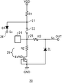
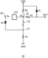
- FIG. 2 is a circuit diagram showing an example of the main body 20 in the trimming circuit 100.
- the trimming circuit 100 includes a fuse resistor 22, a pad for trimming 24, a first diode D1, and an output terminal OUT.
- the trimming circuit 100 may include a first resistance element R1, a second resistance portion 29, a third resistance element R3, and a protection diode ZL.
- the first resistance element R1 is an example of the first resistance part.
- the second resistance portion 29 of this example may include a second resistance element R2 and a resistance element LVND.
- the resistance element LVND is a high resistance element using a transistor.
- the second resistance element R2 and the resistance element LVND are connected in series.
- the third resistance element R3 is an example of the third resistance part.
- the first resistance portion, the second resistance portion, and the third resistance portion are not limited to these cases.
- the trimming circuit 100 is a circuit that outputs a voltage So depending on whether or not the fuse resistor 22 is blown to the output terminal OUT.
- the trimming circuit 100 changes the voltage So applied to the output terminal OUT according to the blow of the fuse resistor 22, and determines on / off of the transistor portion 10 as described above.
- the trimming circuit 100 also changes the voltage So when virtual cutting is executed to generate a state in which the fuse resistor 22 is virtually cut.
- One end of the fuse resistor 22 is connected to the pad 24 at the connection point 28.
- the other end of the fuse resistor 22 is connected to one end of the first diode D1 at the connection point 27.
- the other end of the fuse resistor 22 is connected to the anode of the first diode D1.
- the output terminal OUT is electrically connected to the connection point 28 between the fuse resistor 22 and the pad 24.
- the output terminal OUT is electrically connected to the connection point 28 via the third resistance element R3.
- the output terminal OUT outputs a voltage according to whether or not the fuse resistor 22 is blown.
- first resistance element R1 is connected to the connection point 27 between the fuse resistor 22 and the anode of the first diode D1.
- the other end of the first resistance element R1 is connected to the first potential.
- One end of the second resistor portion 29 is connected to a connection point 28 between one end of the fuse resistor 22 and the pad 24.
- the other end of the second resistance portion 29 is connected to the second potential. That is, one end of the fuse resistor 22 is connected to the second potential via the second resistor portion 29.
- the second resistance element R2 is connected to the connection point 28 and the resistance element LVND is connected to the second potential, but conversely, the resistance element LVND is connected to the connection point 28 and the second resistance element R2. May be connected to the second potential.
- the first potential may be higher than the second potential.
- the second potential corresponds to the potential of the ground wiring GND (ground potential)
- the first potential corresponds to the potential of the high-potential wiring VDD.
- the second potential may be a Lo level substantially equal to the ground potential
- the first potential may be a Hi level substantially equal to the potential of the high potential wiring VDD.
- One end of the fuse resistor 22 may be connected to the high potential wiring VDD via the first resistance element R1.
- the other end of the second resistance portion 29, particularly the gate and drain of the resistance element LVND, may be connected to the ground wiring GND.
- the connection point 27 in this example is a point on the high potential wiring VDD side of the connection point 28.
- the connection point 27 may be arranged between the fuse resistor 22 and the high potential wiring VDD.
- the connection point 28 may be arranged between the fuse resistor 22 and the ground wiring GND.
- the protection diode ZL is connected between the other end of the second resistance portion 29 and the output terminal OUT.
- the anode of the protection diode ZL is connected to the ground wiring GND which is the second potential
- the cathode of the protection diode ZL is connected to the output terminal OUT.
- the fuse resistor 22, the pad for trimming 24, the first diode D1, the first resistance element R1, the second resistance portion 29, the third resistance element R3, and the protection diode ZL may be formed on the semiconductor substrate.
- the transistor portion 10 shown in FIG. 1 may also be formed on the same semiconductor substrate.
- the fuse resistor 22 is, for example, a polysilicon fuse formed of a polysilicon layer.
- the first diode D1 has a second conductive type semiconductor region on the first conductive type semiconductor substrate. In one example, the first conductive type is n-type and the second conductive type is p-type.
- the substrate electrode 26 is an electrode for fixing the potential Sc of the first conductive type semiconductor substrate.
- the substrate electrode 26 may be a back surface electrode arranged on the back surface of the semiconductor substrate, or may be an electrode arranged on the front surface side.
- the first resistor element R1 is a pull-up resistor for pulling up (dividing the voltage) the output terminal OUT to the potential of the high potential wiring VDD when the trimming circuit 100 is not performing trimming, and the fuse resistor 22. It is also a current limiting resistor that limits the current flowing through.
- the second resistor portion 29 is a pull-down resistor for pulling down (dividing the voltage) the output terminal OUT to the ground potential in a state where the fuse resistor 22 is cut.
- the second resistance portion 29 and the third resistance element R3 are also current limiting resistors that limit the current flowing through the fuse resistor 22.
- the level may be adjusted so that the transistor portion 10 is turned on.
- the output voltage S O of the output terminal OUT is pulled up (partial pressure) by the high potential wiring VDD.
- the voltage applied to the high-potential wiring VDD is divided by the first resistance element R1 and the second resistance portion 29.
- the voltage applied to the high-potential wiring VDD is 5V and the electrical resistance values of the first resistance element R1, the second resistance portion 29, and the fuse resistance 22 are 100k ⁇ , 10k ⁇ , and 100 ⁇ , respectively.
- a voltage of about 4.5 V is applied to the output terminal OUT. That is, a voltage So of Hi level (a voltage higher than the threshold voltage of the transistor constituting the transistor unit 10) is applied to the output terminal OUT.
- the transistor portion 10 which is a MOSFET for current adjustment is turned on, and both ends of the corresponding element 2 to be adjusted are maintained in a short state.
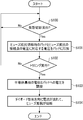
- FIG. 3 is a flowchart showing an example of the trimming method. Virtual disconnection and normal disconnection will be described with reference to FIG.
- the trimming circuit 100 can perform virtual cutting in order to confirm the electrical characteristics of the element 2 to be adjusted after the fuse resistor 22 is blown.
- the trimming circuit 100 creates a state in which the fuse resistor 22 is virtually blown.
- the trimming circuit 100 executes virtual cutting (step S100: YES)
- the voltage Sp applied to the trimming pad 24 may be adjusted.
- the external voltage source or the internal voltage source pads a voltage Sp corresponding to the voltage of the connection point 28 when the fuse resistor 22 is actually connected in order to generate a virtual cut state of the fuse resistor 22.
- Apply to 24 step S101.
- the external voltage source or the internal voltage source may apply the voltage of the ground wiring (for example, 0V voltage) to the pad 24.
- Step S101 is a step of generating a state in which the fuse resistor 22 is virtually cut by applying a predetermined voltage to the pad 24 before the step of passing a forward current through the first diode D1. Correspond.
- a Lo level voltage So is applied to the output terminal OUT in the same manner as when the fuse resistor 22 is blown.
- the transistor portion 10 which is a MOSFET for current adjustment is turned off, and both ends of the corresponding element 2 to be adjusted are not short-circuited. That is, virtual disconnection is realized.
- the characteristics of the adjustment target are measured, and the cutting result of the target fuse resistor 22 is evaluated. If the evaluation result does not satisfy the target and another trimming state can be set, the process branches to the No side in step S102.
- the transistor portion 10, the fuse resistor 22, and the trimming pad 24 may be prepared for each of the plurality of elements 2 to be adjusted and provided in parallel. Also in this case, each fuse resistor 22 can be virtually cut individually.
- Whether or not to perform trimming may be determined based on the result obtained by the virtual disconnection (step S102). For example, the fuse resistor 22 that selectively blows from the plurality of fuse resistors 22 is determined so that the resistance value or the current value between the terminals T1 and the terminal T2 falls within the target range.
- step S102 the potential Sc of the first conductive type semiconductor substrate and the voltage applied to the pad 24 are adjusted so that a forward current flows through the first diode D1 (step S103).
- the substrate electrode 26 of the semiconductor substrate is used as the ground potential.
- a voltage higher than the voltage applied to the high-potential wiring VDD may be applied to the trimming pad 24 by an external voltage source or an internal voltage source.
- a voltage of 10 V or more and 30 V or less is applied to the pad 24 by an external voltage source or an internal voltage source.
- a current flows through the fuse resistor 22, and the fuse resistor 22 is cut by Joule heat (step S104). Since the first diode D1 is connected in the forward direction, a forward current flows to the substrate electrode 26 through the fuse resistor 22 and the first diode D1. Therefore, a current sufficient to blow the fuse resistor 22 can be passed without being affected by the first resistance element R1 and the second resistance portion 29.
- the ground potential to which the second resistor portion 29 is connected may be adjusted.
- the ground potential when a voltage for cutting the fuse resistor 22 is applied to the pad 24, the ground potential may be raised as compared with the case where no voltage is applied to the pad 24. As a result, it is possible to suppress the flow of current from the pad 24 to the second resistance portion 29.
- the ground potential When a voltage for cutting the fuse resistor 22 is applied to the pad 24, the ground potential may be higher than the substrate potential Sc.
- the ground potential may be the same as the high potential wiring VDD. This makes it easier for a current to flow through the fuse resistor 22, and the fuse resistor 22 can be easily blown.
- the trimming circuit 100 is in a state where the fuse resistor 22 is cut off.
- the fuse resistor 22 is blown, the second resistor section 29 pulls down the output terminal OUT to the ground potential.
- a voltage divided by the second resistance portion 29 and the third resistance element R3 is applied to the output terminal OUT. Therefore, a Lo level voltage So is applied to the output terminal OUT.
- the transistor portion 10 which is a MOSFET for current adjustment is turned off, and both ends of the corresponding element 2 to be adjusted are changed to a state in which they are not short-circuited.
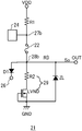
- FIG. 4 is a circuit diagram showing an example of the main body 21 of the trimming circuit of the comparative example.
- the trimming pad 24 is connected to the connection point 27b between the fuse resistor 22 and the first resistance element R1, and the connection point 28b between the fuse resistor 22 and the second resistance portion 29 is connected to the first. 1 diode D1 is connected.
- the output terminal OUT is connected to the connection point 28b between the first diode D1 and the fuse resistor 22.
- the pad 24 and the output terminal OUT are electrically separated from each other when the fuse resistor 22 is blown.
- the pad 24 and the output terminal OUT are electrically connected even when the fuse resistor 22 is blown. Therefore, the trimming pad 24 can be reused for monitoring the voltage at the output terminal OUT. Specifically, the voltage So at the output terminal OUT can be measured even after trimming. In addition, the presence or absence of deterioration (leakage) caused by trimming on the element can be confirmed, and high reliability in the circuit can be ensured.
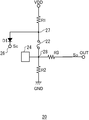
- FIG. 5 is a circuit diagram showing another example of the main body 20 in the trimming circuit 100.
- the main body 20 shown in FIG. 5 has a structure similar to that of the main body 20 shown in FIG. 2, except that the protection diode ZL is omitted.
- FIG. 6 is an example of the semiconductor device 200 to which the trimming circuit 100 is applied.
- the trimming circuit 100 of this embodiment can be applied to various semiconductor devices 200.
- the output stage circuit unit 210 and the control circuit unit 230 are formed on the same semiconductor substrate 30.
- the semiconductor device 200 is an IPS (intelligent power switch).
- the output stage circuit unit 210 may include a trench gate type power semiconductor.
- the output stage circuit unit 210 may be a vertical MOSFET (metal-oxide-semiconductor field-effect transistor) or an IGBT (insulated gate bipolar transistor). In this example, it is a vertical MOSFET having a trench gate.
- the conductive type of the semiconductor substrate 30 is n type.
- the semiconductor substrate 30 includes an n-type drift layer 201.
- An n + type layer as the contact layer 202 is formed on one surface (back surface in the figure) of the semiconductor substrate 30 by diffusion of impurities or the like.
- a drain electrode 203 is formed on the contact layer 202.
- the drain electrode 203 is formed of a conductive material such as metal.
- the main surface on which the drain electrode 203 is formed is referred to as a back surface, and the main surface on the opposite side of the back surface is referred to as a front surface.
- a p-type base layer 212 is formed on the front surface, which is the other surface of the semiconductor substrate 30.
- an n + type layer 214 is formed so as to surround the p + type layer 213.
- a trench gate is formed on the semiconductor substrate 30. The trench gate penetrates the p-type base layer 212 and reaches the n-type drift layer 201.
- the trench gate includes a conductive portion 215 filled in the trench and an insulating film 216 that electrically separates the conductive portion 215 from the semiconductor substrate 30.
- the source electrode 220 is formed so as to cover the p + type layer 213.
- the source electrode 220 is made of a conductive material.
- An insulating film 222 is formed above the trench gate. The insulating film 222 insulates the trench gate and the source electrode 220.
- n displayed as a component means an element having a large number of electrons as a carrier
- p means an element having a large number of holes
- + means a relatively high impurity concentration.
- Means that, and "-” means that the impurity concentration is relatively low.
- the control circuit unit 230 may include a CMOS circuit unit in which an n-channel type MOS transistor 240 and a p-channel type MOS transistor 250 are combined on the front surface side of the semiconductor substrate 30.
- the n-channel type MOS transistor 240 has a p-well region 241 formed in the n-type semiconductor substrate 30.
- An n + type source region 242 and a drain region 243 are formed inside the p-well region 241, respectively.
- the source electrode 246 is connected to the source region 242, and the drain electrode 247 is connected to the drain region 243.
- the source electrode 246 and the drain electrode 247 are formed of a conductive material such as metal.
- a gate electrode 244 is provided on the front surface of the semiconductor substrate 30 via a gate insulating film 245.
- a source region 242 is provided on one side of the gate electrode 244, and a drain region 243 is provided on the other side of the gate electrode 244.
- the p-channel type MOS transistor 250 has a p-well region 251 formed in the n-type semiconductor substrate 30, and has an n-well region 252 inside the p-well region 251.
- a p + type source region 253 and a drain region 254 are formed inside the n-well region 252, respectively.
- the source electrode 257 is connected to the source region 253, and the drain electrode 258 is connected to the drain region 254.
- a gate electrode 255 is provided on the front surface of the semiconductor substrate 30 via a gate insulating film 256.
- the trimming circuit 100 may be configured on the semiconductor substrate 30 in the above-mentioned semiconductor device 200.
- the trimming circuit 100 may be used to set various voltages in the semiconductor device 200.
- FIG. 7 is a cross-sectional view showing an example of a vertical diode used in the trimming circuit 100.
- the first diode D1 is formed on the semiconductor substrate 30.
- the semiconductor substrate 30 is an n-type semiconductor substrate 30.
- a second conductive type first semiconductor region 42 is formed on the front surface side of the semiconductor substrate 30.
- the first semiconductor region 42 is a p-type diffusion layer formed on the n-type semiconductor substrate 30.
- a PN junction is formed by the first semiconductor region 42 and the semiconductor substrate 30. This PN junction functions as the first diode D1.
- the first diode D1 may be a vertical diode.
- the vertical diode means a diode in which a current flows in the thickness direction of the semiconductor substrate 30.
- the anode is arranged on the front surface side of the semiconductor substrate 30, and the cathode is arranged on the back surface side of the semiconductor substrate 30.
- a substrate electrode 26 is connected to the cathode.
- the substrate electrode 26 may be provided on the front surface side of the semiconductor substrate 30 because the potential of the semiconductor substrate 30 may be fixed.
- a second conductive type second semiconductor region 44 may be formed in a part of the first semiconductor region 42.
- the second semiconductor region 44 has a higher impurity concentration than the first semiconductor region 42.
- the second semiconductor region 44 is a p + diffusion layer.
- An insulating film 46 is partially provided on the semiconductor substrate 30.
- the insulating film 46 may be a LOCOS oxide film.
- FIG. 8 is a cross-sectional view showing an example of a diffusion diode as a comparative example.
- the diffuse diode has a p-well region 52 in the semiconductor substrate 30. Then, an n-type cathode region 53 and a p + -type anode region 54 are formed in the p-well region 52.
- the n-type drift layer 201, the p-well region 52, and the n-type cathode region 53 of the semiconductor substrate 30 operate as vertical npn parasitic transistors. It ends up.
- FIG. 9 is a cross-sectional view showing an example of a polysilicon diode as a comparative example.
- the polysilicon diode has polysilicon 60 arranged on the semiconductor substrate 30 via an insulating layer 62. Impurities are doped in polysilicon 60 to form p-type regions, n-type regions, and n + -type regions. An anode electrode is formed in the p-type region, and a cathode electrode is formed in the n + type region.
- the operating resistance becomes large. Therefore, in order to lower the resistance value, the area occupied by the polysilicon 60 must be increased. Therefore, it is difficult to prevent the expansion of the circuit area.
- the vertical diode described above with reference to FIG. 7 When the vertical diode described above with reference to FIG. 7 is used as the first diode D1, there is no parasitic operation and the operating resistance is smaller than that of the polysilicon diode. Therefore, it is desirable to use a vertical diode as the first diode D1 in which a current flows in the forward direction to blow the fuse resistor 22.
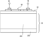
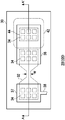
- FIG. 10 is a plan view showing a configuration example of the main body 20.
- FIG. 11 is a cross-sectional view showing a configuration example of the main body portion 20.
- FIG. 11 shows a cross section of the main body 20 along the AA'line in FIG.
- the first resistance element R1, the second resistance unit 29, the third resistance element R3, and the protection diode ZL are omitted in FIG. 10 for convenience of explanation, and in FIG. 11, only the electrical connection relationship is shown by the circuit symbol. ing.
- the transistor portion 10, the first resistance element R1, the second resistance portion 29, the third resistance element R3, and the protection diode ZL may be formed on the actual semiconductor substrate 30.
- the first diode D1 and the fuse resistor 22 are formed on the semiconductor substrate 30.
- the semiconductor substrate 30 is a first conductive type semiconductor substrate 30.
- the first diode D1 is the vertical diode described in FIG. 7.
- a contact portion 34 is connected to the second semiconductor region 44 of the second conductive type.
- the contact portion 34 may be formed of a conductive material.
- the polysilicon layer 32 is provided on the semiconductor substrate 30 via the insulating film 46.
- the fuse resistor 22 is formed of a polysilicon layer 32.
- the fuse resistor 22 is formed with a narrow width W at the center so that it can be easily blown.
- one end of the fuse resistor 22 is connected to the metal wiring 36 via the contact portion 34.
- the insulating film 46 is partially removed, and the second semiconductor region 44 is partially exposed.
- the second semiconductor region 44 is connected to the metal wiring 36 via the contact portion 34.
- the metal wiring 36 and the contact portion 34 electrically connect the anode of the first diode D1 and the fuse resistor 22, and function as the connection point 27 shown in FIG.
- the metal wiring 36 may be connected to the high potential wiring VDD via the first resistance element R1.
- the other end of the fuse resistor 22 is connected to the metal wiring 37 via the contact portion 34.
- the metal wiring 37 functions as a connection point 28 for connecting the fuse resistor 22 to the pad 24 and the second resistor portion 29.
- the metal wiring 37 may have a connecting portion 38 that connects to the trimming pad 24.
- the metal wiring 37 may be electrically connected to the output terminal OUT via the third resistance element R3. Further, the metal wiring 37 may be electrically connected to the ground potential GND via the second resistance portion 29.
- An interlayer insulating film 47 may be formed between the polysilicon layer 32, the second semiconductor region 44, the insulating film 46, and the metal wirings 36 and 37. That is, the metal wiring 36 and the metal wiring 37 may be formed on the interlayer insulating film 47. In this case, the contact portion 34 is formed through the opening in the interlayer insulating film 47.
- the trimming circuit 100 of this example virtual cutting can be realized in which the electrical characteristics of the element to be adjusted are confirmed after the fuse resistor 22 is blown before the fuse resistor 22 is blown.
- the trimming pad 24 connected to one end of the fuse resistor 22 is required, but the existing substrate electrode 26 such as the back electrode may be used as the terminal on the other end side of the fuse resistor 22. It can be done, and there is no need to provide an external terminal dedicated to trimming. Further, it is not necessary to provide a resistance bypass circuit that can withstand a large current that blows the fuse resistor 22. Therefore, it is possible to realize the trimming circuit 100 that has both miniaturization and a virtual cutting function as compared with the conventional case.
- the first diode D1 has a second conductive type first semiconductor region 42 formed on the first conductive type semiconductor substrate 30.
- the first diode D1 may not be formed by the polysilicon layer 32 but may be formed by an impurity diffusion layer formed on the semiconductor substrate 30. Therefore, since the fuse resistor 22 and the first diode D1 are not formed in the same layer, they may be formed in a laminated manner. As a result, the area on the semiconductor substrate 30 can be effectively utilized to reduce the area of the trimming circuit 100.
- the trimming circuit 100 of this example even if the fuse resistor 22 is blown, the pad 24 and the output terminal OUT are electrically connected via the metal wiring 37 and the third resistance element R3. Therefore, the trimming pad 24 can be reused for monitoring the voltage at the output terminal OUT. Specifically, the voltage So at the output terminal OUT can be measured even after trimming. In addition, the presence or absence of deterioration (leakage) caused by trimming on the element can be confirmed, and high reliability in the circuit can be ensured.
- FIG. 12 is a circuit diagram showing an example of the main body 20 using the p-type semiconductor substrate 30.
- the first conductive type is the p type and the second conductive type is the n type. Therefore, in the main body 20 of this example, in the configurations shown in FIGS. 7, 10, and 11, the n-type semiconductor substrate 30 is the p-type semiconductor substrate 30, and the p-type first semiconductor region 42 is the n-type semiconductor. It has a configuration in which the p + type second semiconductor region 44 is defined as an n + type semiconductor region. Due to the orientation of the PN junction, the substrate electrode 26 side becomes the anode. Other configurations are the same as those shown in FIGS. 7, 10, and 11.
- the trimming circuit 100 of this example includes a fuse resistor 22, a pad for trimming 24, a first diode D1, a first resistor element R1, a second resistor element R2, a third resistor element R3, and a protection diode Di.
- One end of the fuse resistor 22 is connected to the pad 24.
- the other end of the fuse resistor 22 is connected to one end of the first diode D1.
- the other end of the fuse resistor 22 is connected to the cathode of the first diode D1.
- first resistance element R1 is connected to a connection point 27 between one end of the fuse resistor 22 and the cathode of the first diode D1.
- the other end of the first resistance element R1 is connected to the first potential.
- the first potential may be the ground potential GND.
- One end of the second resistance element R2 is connected to the connection point 28 between the fuse resistor 22 and the pad 24.
- the other end of the second resistance element R2 is connected to the second potential.
- the second potential is the potential of the high potential wiring.
- the output terminal OUT is electrically connected to the connection point 28 between the fuse resistor 22 and the pad 24.
- the output terminal OUT is electrically connected to the connection point 28 via the third resistance element R3. The output terminal OUT outputs a voltage according to whether or not the fuse resistor 22 is blown.
- FIG. 13 is a circuit diagram showing a comparative example of the main body 20 using the p-type semiconductor substrate 30.
- a trimming pad 24 is connected to one end of the fuse resistor 22, and a first diode D1 is connected to the other end of the fuse resistor 22.
- the output terminal OUT is connected to the connection point 27b between the first diode D1 and the fuse resistor.
- the trimming pad 24 is provided only at one end of the fuse resistor 22, it is possible to prevent the circuit area from expanding.
- the pad 24 and the output terminal OUT are electrically separated from each other when the fuse resistor 22 is blown.
- the pad 24 and the output terminal OUT are electrically connected even when the fuse resistor 22 is blown. Therefore, the trimming pad 24 can be reused for monitoring the voltage at the output terminal OUT. Specifically, the voltage So at the output terminal OUT can be measured even after trimming. In addition, the presence or absence of deterioration (leakage) caused by trimming on the element can be confirmed, and high reliability in the circuit can be ensured.
- the trimming circuit 100 of this example can also realize virtual cutting for confirming the electrical characteristics of the element to be adjusted after cutting the fuse resistor 22 before cutting the fuse resistor 22.
- the external voltage source or the internal voltage source applies a voltage Sp corresponding to the voltage at the connection point 28 between the pad 24 and the fuse resistor 22 to the pad 24 when the fuse resistor 22 is blown.
- the first resistor element R1 pulls up (divides) the connection point 28 to the potential of the high potential wiring VDD. Therefore, the external voltage source or the internal voltage source may apply the voltage of the high potential wiring VDD to the pad 24.
- the existing substrate electrode 26 such as the back surface electrode can be utilized as the control terminal of the fuse resistor 22, and the number of external terminals dedicated to trimming can be reduced. Further, it is not necessary to provide a resistance bypass circuit that can withstand a large current that blows the fuse resistor 22. Therefore, it is possible to realize a trimming circuit 100 having a small circuit area and capable of virtual cutting. Further, according to the main body 20 of the trimming circuit 100 shown in FIG. 12, the pad 24 and the output terminal OUT are electrically connected even when the fuse resistor 22 is blown. Therefore, the trimming pad 24 can be reused for monitoring the voltage at the output terminal OUT.
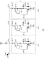
- FIG. 14 is a diagram showing another configuration example of the trimming circuit 100.
- the trimming circuit 100 of this example includes a plurality of main bodies 20.
- the trimming circuit 100 of this example includes main body portions 20-1, 20-2, 20-3, ....
- the k-th main body portion 20 may be referred to as a main body portion 20-k.
- a branch number of k is attached to the code of each component in the main body portion 20-k.
- Each main body 20 is provided corresponding to the element 2 to be adjusted.
- Each main body 20 may be connected to the gate of the transistor 10 shown in FIG.
- each main body 20 has the same structure as the main body 20 of any of the embodiments described with reference to FIGS. 1 to 13.
- each main body 20 has the same structure as the main body 20 shown in FIG.
- the third resistance element R3 is omitted.
- the main body 20 in each embodiment may or may not have the third resistance element R3.
- the second resistance element R2 is arranged between the pad 24 and the output terminal OUT.
- the second resistance element R2 may be arranged between the pad 24 and the output terminal OUT as in FIG. 14, and between the pad 24 and the resistance element LVND as in FIG. It may be placed in.
- the first diode D1 is commonly provided for the plurality of main bodies 20. That is, each main body 20 is not provided with a separate first diode D1.
- the common first diode D1 is connected to the fuse resistor 22 of each main body 20.
- the anode is connected to a plurality of fuse resistors 22.
- One end of the fuse resistor 22-k of this example is connected to the pad 24-k, and the other end is connected to the first diode D1.
- the output terminal OUTk and the resistance element LVNDk are connected to the one end of the fuse resistor 22-k via the second resistance element R2-1.
- the first resistance element R1 is connected to the other end of the fuse resistance 22-k.
- the first resistance element R1 is also provided in common with the plurality of main body portions 20.
- One end of the first resistance element R1 is connected to the first diode D1, and the other end is connected to the high potential wiring VDD.
- a connection point 27-k is provided for each main body portion 20-k. The anode of the first diode D1, one end of the first resistance element R1, and the other end of the fuse resistor 22-k are connected to the connection point 27-k.
- the scale of the device can be reduced. Further, by providing the first resistance element R1 in common to the plurality of main body portions 20, the scale of the apparatus can be reduced.
- the fuse resistors 22 to be cut are selected one by one, and a predetermined high voltage is sequentially applied to the pads 24-k corresponding to the fuse resistors 22-k to be cut.
- the operation of connecting the fuse resistor 22 in each main body 20 is the same as the example of FIG.
- the high voltage is a voltage higher than the voltage applied to the high potential wiring VDD.
- a ground potential may be applied to the unselected pads 24.
- the ground potential applied to the main body 20 selected to cut the fuse resistor 22 may be changed. For example, when the fuse resistor 22-k is blown, the ground potential applied to the main body 20-k is increased.
- the ground potential of the main body 20-k may be controlled to the same potential as the potential applied to the pad 24-k. As a result, it is possible to suppress the flow of current from the pad 24-k to the second resistance portion 29-k.
- each main body 20 can be set in the virtual disconnect state in parallel. Further, a part of the main body 20 may be selectively set to the virtual disconnection state.
- the resistance values of the first resistance element R1 and the second resistance element R2 may be sufficiently smaller than the resistance values of the resistance element LVND. By increasing the resistance value of the resistance element LVND, the current flowing through the main body 20 can be reduced.
- FIG. 15 is a diagram showing another configuration example of the trimming circuit 100.
- the trimming circuit 100 of this example includes a plurality of main bodies 20.
- the first diode D1 and the first resistance element R1 are commonly provided for the plurality of main body portions 20 as in the example of FIG.
- the first diode D1 of this example is connected to each fuse resistor 22-k and a connection point 27-k with the ground potential. Further, the first resistance element R1 is connected between each connection point 27 and the ground potential.
- the main body 20 of this example outputs a voltage corresponding to the high voltage VDD from the output terminal OUT when the fuse resistor 22 is blown. Further, the main body 20 of this example outputs a voltage corresponding to the ground potential from the output terminal OUT when the fuse resistor 22 is not blown.
- each main body 20 the fuse resistor 22, the first diode D1 and the first resistance element R1 are connected. One end of each fuse resistor 22-k is connected to the pad 24-k, and the other end is connected to the first diode D1 and the first resistance element R1.
- the second resistance element R2-k is connected to the connection point 28-k between the pad 24-k and the fuse resistor 22-k. One end of the second resistance element R2-k is connected to the connection point 28-k, and the other end is connected to the resistance element LVNDk.
- One end of the resistance element LVNDk is connected to the second resistance element R2-k, and the other end is connected to the high potential wiring VDD.
- the connection point between the resistance element LVNDk and the second resistance element R2-k is connected to the output terminal OUTk.
- a protection diode ZL may be provided between the output terminal OUTk and the ground potential.
- the scale of the device can be reduced by providing the first diode D1 in common for the plurality of main bodies 20. Further, by providing the first resistance element R1 in common to the plurality of main body portions 20, the scale of the apparatus can be reduced.
- the fuse resistors 22 to be cut are selected one by one, and a predetermined high voltage is sequentially applied to the pads 24-k corresponding to the fuse resistors 22-k to be cut.
- the high voltage may be higher than the voltage applied to the high potential wiring VDD.
- a ground potential may be applied to the unselected pads 24.
- the ground potential applied to the main body 20 selected to cut the fuse resistor 22 may be increased.
- the ground potential may be increased even in the main body portion 20 which is not selected.
- a voltage for virtual disconnection may be applied to each pad 24 in parallel. That is, each main body 20 can be set in the virtual disconnect state in parallel. Further, a part of the main body 20 may be selectively set to the virtual disconnection state.
- FIG. 16 is a diagram showing another configuration example of the trimming circuit 100.
- the trimming circuit 100 of this example differs from the example of FIG. 14 in that the directions of the anode and the cathode of the first diode D1 are reversed from the example of FIG.
- Other structures are similar to the example in FIG. That is, in the first diode D1 of this example, the fuse resistor 22 of each main body 20 is connected to the cathode, and the substrate potential Sc is applied to the anode.
- One end of each fuse resistor 22-k is connected to the pad 24-k, and the other end is connected to the cathode of the first diode D1 via a connection point 27-k.
- a low voltage is selectively applied to the pad 24-k of the main body 20-k that cuts the fuse resistor 22-k.
- the low voltage is such that a forward current flows from the first diode D1 to the pad 24-k. That is, the low potential is lower than the forward voltage of the first diode D1 with respect to the substrate voltage Sc.
- the low voltage is a voltage lower than the ground potential.
- FIG. 17 is a diagram showing another configuration example of the trimming circuit 100.
- the trimming circuit 100 of this example differs from the example of FIG. 15 in that the directions of the anode and the cathode of the first diode D1 are reversed from the example of FIG.
- Other structures are similar to the example in FIG. That is, in the first diode D1 of this example, the fuse resistor 22 of each main body 20 is connected to the cathode, and the substrate potential Sc is applied to the anode.
- One end of each fuse resistor 22-k is connected to the pad 24-k, and the other end is connected to the cathode of the first diode D1 via a connection point 27-k.
- a low voltage is selectively applied to the pad 24-k of the main body 20-k that cuts the fuse resistor 22-k.
- the low voltage is such that a forward current flows from the first diode D1 to the pad 24-k. That is, the low potential is lower than the forward voltage of the first diode D1 with respect to the substrate voltage Sc.
- the low voltage is a voltage lower than the ground potential.
- a voltage for virtual disconnection may be applied to each pad 24 in parallel. That is, each main body 20 can be set in the virtual disconnect state in parallel. Further, a part of the main body 20 may be selectively set to the virtual disconnection state.
- FIG. 18 is a diagram showing another configuration example of the first diode D1.
- the first diode D1 in each embodiment may have the structure of FIG.
- the first diode D1 of this example is formed on the semiconductor substrate 30. As shown in FIG. 6 and the like, the semiconductor substrate 30 may be formed with elements other than the first diode D1.
- the semiconductor substrate 30 is an n-type semiconductor substrate 30.
- a p-type first semiconductor region 42 is formed on the front surface side of the semiconductor substrate 30.
- a PN junction is formed by the first semiconductor region 42 and the semiconductor substrate 30. This PN junction functions as the first diode D1.
- the first diode D1 may be a vertical diode.
- the anode is arranged on the front surface side of the semiconductor substrate 30, and the cathode is arranged on the back surface side of the semiconductor substrate 30.
- a substrate electrode 26 is connected to the cathode.
- the substrate electrode 26 may be provided on the front surface side of the semiconductor substrate 30 because the potential of the semiconductor substrate 30 may be fixed.
- a p + type second semiconductor region 44 may be formed in a part of the first semiconductor region 42.
- the second semiconductor region 44 has a higher impurity concentration than the first semiconductor region 42.
- An insulating film 46 is partially provided on the semiconductor substrate 30.
- the insulating film 46 may be a LOCOS oxide film.
- the insulating film 46 exposes at least a part of the second semiconductor region 44.
- a polysilicon layer 32 that functions as wiring may be provided above the insulating film 46.
- An interlayer insulating film 47 is provided so as to cover the insulating film 46, the second semiconductor region 44, and the polysilicon layer 32.
- the interlayer insulating film 47 is formed with through holes for forming the contact portion 34.
- a metal wiring 36 is provided on the interlayer insulating film 47. The metal wiring 36 is connected to the polysilicon layer 32 and the second semiconductor region 44 by the contact portion 34.
- FIG. 19 is a diagram illustrating the protection diode ZL and the protection diode Di.
- the protection diode provided between the output terminal OUT and the ground potential GND is referred to as the protection diode Di
- the protection diode provided between the output terminal OUT and the high potential wiring VDD is referred to as the protection diode ZL.
- Each main body 20 may be provided with one or both of the protection diode Di and the protection diode ZL.
- the output terminal OUT When the transistor unit 10 connected to the output terminal OUT includes an n-channel MOS transistor, the output terminal OUT may be provided with a protection diode ZL. As a result, it is possible to prevent an excessively high voltage from being applied to the transistor portion 10.
- the output terminal OUT When the transistor unit 10 connected to the output terminal OUT includes a p-channel MOS transistor, the output terminal OUT may be provided with a protection diode Di. As a result, it is possible to prevent an excessively low voltage from being applied to the transistor portion 10.
- the transistor unit 10 includes both an n-channel MOS transistor such as a CMOS circuit and a p-channel MOS transistor, both the protection diode Di and the protection diode ZL may be provided.
- a protection diode Di may be provided in a part of the main body 20, and a protection diode ZL may be provided in a part of the main body 20. Further, both the protection diode Di and the protection diode ZL may be provided in all the main body portions 20.
- insulation Layer 100 ... trimming circuit, 200 ... semiconductor device, 201 ... drift layer, 202 ... contact layer, 203 ... drain electrode, 210 ... output stage circuit section, 212 ... p-type base layer, 213 ... p + type layer, 214 ... n + type layer, 215 ... conductive part, 216 ... insulating film, 220 ... source electrode, 222 ... insulating film, 230 ... control circuit unit, 240 ... MOS transistor, 241 ... p-well region, 242 ... source region, 243 ... drain region, 244 ... gate electrode, 245 ... gate insulating film , 246 ... source electrode, 247 ... drain electrode, 250 ... MOS transistor, 251 ... p-well region, 252 ... n-well region, 253 ... source region, 254 ... drain Region, 255 ... Gate electrode, 256 ... Gate insulating film, 257 ... Source electrode, 258 ... Drain electrode
Landscapes
- Semiconductor Integrated Circuits (AREA)
- Metal-Oxide And Bipolar Metal-Oxide Semiconductor Integrated Circuits (AREA)
Abstract
ヒューズ抵抗の切断の有無に応じた電圧を出力するトリミング回路であって、半導体基板に絶縁膜を介して配置されるポリシリコン層により形成されるヒューズ抵抗と、ヒューズ抵抗の一端に接続されるトリミング用のパッドと、ヒューズ抵抗とパッドとの接続点に電気的に接続されており、ヒューズ抵抗の切断の有無に応じた電圧を出力する出力端子と、半導体基板に形成されており、ヒューズ抵抗の他端に一端が接続されるダイオードと、を備えているトリミング回路を提供する。
Description
本発明は、トリミング回路およびトリミング方法に関する。
半導体集積回路における製造バラつきによる回路特性の変動を補正するために、トリミング回路が用いられる。トリミング回路として、ポリシリコン層により形成されたヒューズ抵抗を備える回路が知られている(例えば、特許文献1)。また、ヒューズ抵抗の両端のそれぞれにトリミング専用の外部端子を設けたトリミング回路が知られている(例えば、特許文献2)。
[先行技術文献]
[特許文献]
[特許文献1] 特開2018-22848号公報
[特許文献2] 特開2000-340656号公報
[先行技術文献]
[特許文献]
[特許文献1] 特開2018-22848号公報
[特許文献2] 特開2000-340656号公報
トリミング回路は、ヒューズ抵抗の切断の有無により出力端子の電圧が変動する本体部と、本体部の出力電圧によって特性が変動する調整部とを有する。トリミングが実行されて、ヒューズ抵抗が切断された後においても、本体部の出力端子の電圧を確認できることが望ましい。
本発明の一態様は、トリミング回路を提供する。トリミング回路は、ヒューズ抵抗の切断の有無に応じた電圧を出力する本体部を備えてよい。本体部は、ヒューズ抵抗と、トリミング用のパッドと、出力端子と、ダイオードと、を備えてよい。ヒューズ抵抗は、半導体基板に絶縁膜を介して配置されるポリシリコン層により形成されてよい。パッドは、ヒューズ抵抗の一端に接続されてよい。出力端子は、ヒューズ抵抗とパッドとの接続点に電気的に接続されてよい。出力端子は、ヒューズ抵抗の切断の有無に応じた電圧を出力してよい。ダイオードは、半導体基板に形成されてよい。ダイオードは、ヒューズ抵抗の他端に一端が接続されてよい。
ダイオードは、第1導電型の半導体基板に形成された第2導電型の半導体領域を有してよい。
トリミング回路は、第1抵抗部を備えてよい。第1抵抗部の一端は、ヒューズ抵抗とダイオードとの接続点に接続されてよい。第1抵抗部の他端は、第1電位に接続されてよい。
トリミング回路は、第2抵抗部を備えてよい。第2抵抗部の一端は、ヒューズ抵抗とパッドとの接続点に接続されてよい。第2抵抗部の他端は、第2電位に接続されてよい。
トリミング回路は、保護ダイオードを備えてよい。保護ダイオードは、第2抵抗部の他端と出力端子との間に接続されてよい。
トリミング回路は、トランジスタ部を備えてよい。トランジスタ部は、半導体基板に形成されてよい。本体部の出力端子に、トランジスタ部の制御端子が接続されてよい。
ダイオードは、縦型ダイオードであってよい。ダイオードの他端が、半導体基板の基板電極に接続されてよい。
第1導電型は、n型であってよい。第2導電型は、p型であってよい。ヒューズ抵抗の他端とダイオードのアノードとが接続されてよい。トリミング回路は、第1抵抗部を備えてよい。第1抵抗部の一端は、ヒューズ抵抗とダイオードのアノードとの接続点に接続されてよい。第1抵抗部の他端は、高電位配線に接続されてよい。トリミング回路は、第2抵抗部を備えてよい。第2抵抗部の一端は、ヒューズ抵抗とパッドとの接続点に接続されてよい。第2抵抗部の他端は、グランド配線に接続されてよい。
第1導電型は、p型であってよい。第2導電型は、n型であってよい。ヒューズ抵抗の他端とダイオードのカソードとが接続されてよい。トリミング回路は、第1抵抗部を備えてよい。第1抵抗部の一端は、ヒューズ抵抗とダイオードのカソードとの接続点に接続されてよい。第1抵抗部の他端は、グランド配線に接続されてよい。トリミング回路は、第2抵抗部を備えてよい。第2抵抗部の一端は、ヒューズ抵抗とパッドとの接続点に接続されてよい。第2抵抗部の他端は、高電位配線に接続されてよい。
トリミング回路は、複数の本体部を備えてよい。ダイオードが、複数の本体部に対して共通に設けられてよい。ダイオードには、それぞれの本体部のヒューズ抵抗の他端が接続されていてよい。
トリミング回路は、複数の本体部に対して共通に設けられ、ダイオードに一端が接続され、他端が高電位配線に接続される第1抵抗部を備えてよい。第1抵抗部の一端には、それぞれの本体部のヒューズ抵抗の他端が接続されていてよい。
トリミング回路は、複数の本体部に対して共通に設けられ、ダイオードに一端が接続され、他端がグランド配線に接続される第1抵抗部を備えてよい。第1抵抗部の一端には、それぞれの本体部のヒューズ抵抗の他端が接続されていてよい。
ダイオードのカソードに、それぞれの本体部のヒューズ抵抗の他端が接続されていてよい。
ダイオードのアノードに、それぞれの本体部のヒューズ抵抗の他端が接続されていてよい。
本発明の他の態様は、上記のトリミング回路を用いて、被調整素子の電気特性を調整するトリミング方法であってよい。トリミング方法は、ダイオードに順方向電流が流れるように半導体基板の電位と、パッドに印加する電圧を調整する段階を備えてよい。トリミング方法は、順方向電流がヒューズ抵抗を流れることによってヒューズ抵抗を切断する段階を備えてよい。
トリミング方法は、ダイオードに順方向電流を流す段階の前に、パッドに、予め定められた電圧を印加することにより、ヒューズ抵抗が仮想的に切断された状態を生成する段階を備えてよい。
ヒューズ抵抗を切断した後において、パッドと出力端子とは電気的に接続されていてよい。
電圧を調整する段階において、ヒューズ抵抗を切断すべき本体部のパッドに、選択的に電圧を印加してよい。
それぞれの本体部には、高電位およびグランド電位が印加されてよい。電圧を調整する段階において、ヒューズ抵抗を切断すべき本体部に印加するグランド電位を変更してよい。
なお、上記の発明の概要は、本発明の必要な特徴の全てを列挙したものではない。また、これらの特徴群のサブコンビネーションもまた、発明となりうる。
以下、発明の実施の形態を通じて本発明を説明するが、以下の実施形態は請求の範囲にかかる発明を限定するものではない。また、実施形態の中で説明されている特徴の組み合わせの全てが発明の解決手段に必須であるとは限らない。
図1は、本発明の一実施形態に係るトリミング回路100の概略構成を示す図である。トリミング回路100は、一例において、内部端子T1、T2間の抵抗値を調整する。内部端子T1、T2間には、被調整素子として抵抗が接続されている。内部端子T1およびT2の間には、複数の被調整素子2が直列接続されてよい。トリミング回路100は、それぞれの被調整素子2の両端を、短絡するか否かを切り替えることで、内部端子T1、T2間の抵抗値を調整してよい。被調整素子2の数および抵抗値は、適宜に変更されてよい。また、被調整素子2は、抵抗に限られず、MOSFET等の他の素子であってもよい。この場合、トリミング回路100は、例えばMOSFETが直列接続した直列MOSFET回路の電気特性を調整する。
本例において、トリミング回路100は、本体部20とトランジスタ部10とを備える。本例では、一つの本体部20と、一つのトランジスタ部10とが一つのセットになっている。トリミング回路100は、複数セットの本体部20およびトランジスタ部10を備えてよい。本体部20とトランジスタ部10のセット数は、適宜に変更されてよい。本体部20とトランジスタ部10のセット数が増えるほど、端子T1、T2間の抵抗、電流等の電気特性をきめ細かく調整することができ、調整精度を高めることができる。
トランジスタ部10は、MOSトランジスタであってよい。例えば、図1に示すトランジスタ部10は、nチャネル型MOSFETである。トランジスタ部10のドレイン12とソース13との間に被調整素子2が設けられる。すなわち、電流等の電気特性を調整したい被調整素子2とトランジスタ部10とが並列に接続される。トランジスタ部10のゲート11は、本体部20の出力端子OUTに接続されてよい。トランジスタ部10は、半導体基板に形成され、本体部20の出力端子OUTに制御端子(ゲート端子)が接続されるスイッチング素子の一例である。
本例では、本体部20の出力端子OUTがLoレベル(低レベル)になると、トランジスタ部10はオフになる。これにより、対応する被調整素子2の両端は短絡されていない状態となる。一方、本体部20の出力端子OUTがHiレベル(高レベル)になると、トランジスタ部10はオンとなる。トランジスタ部10がオンとなると、対応する被調整素子2の両端はショート(短絡)状態となる。但し、この場合に限られず、本体部20の出力端子OUTがLoレベルになるとトランジスタ部10がオンとなり、本体部20の出力端子OUTがHiレベルになると、トランジスタ部10がオフとなるようにトランジスタ部10を構成してもよい。
図2は、トリミング回路100における本体部20の一例を示す回路図である。トリミング回路100は、ヒューズ抵抗22、トリミング用のパッド24、第1ダイオードD1、および出力端子OUTを備える。トリミング回路100は、第1抵抗素子R1、第2抵抗部29、第3抵抗素子R3、および保護ダイオードZLを備えてよい。第1抵抗素子R1は、第1抵抗部の一例である。本例の第2抵抗部29は、第2抵抗素子R2と、抵抗素子LVNDとを備えてよい。抵抗素子LVNDは、トランジスタを用いた高抵抗素子である。本例では、第2抵抗素子R2と抵抗素子LVNDとが直列に接続されている。第3抵抗素子R3は、第3抵抗部の一例である。但し、第1抵抗部、第2抵抗部、および第3抵抗部は、これらの場合に限られない。
トリミング回路100は、ヒューズ抵抗22の切断の有無に応じた電圧Soを出力端子OUTへ出力する回路である。トリミング回路100は、ヒューズ抵抗22の切断に応じて出力端子OUTへ印加される電圧Soを変化させて、上述したとおりトランジスタ部10のオン・オフを決定する。また、ヒューズ抵抗22が仮想的に切断された状態を生成する仮想切断が実行される場合にも、トリミング回路100は、電圧Soを変化させる。
ヒューズ抵抗22の一端は、接続点28においてパッド24と接続されている。ヒューズ抵抗22の他端は、接続点27において第1ダイオードD1の一端に接続されている。本例では、ヒューズ抵抗22の他端は、第1ダイオードD1のアノードに接続されている。出力端子OUTは、ヒューズ抵抗22とパッド24との接続点28に電気的に接続されている。本例では、出力端子OUTは、第3抵抗素子R3を介して接続点28に電気的に接続されている。出力端子OUTは、ヒューズ抵抗22の切断の有無に応じた電圧を出力する。
第1抵抗素子R1の一端は、ヒューズ抵抗22と第1ダイオードD1のアノードとの接続点27に接続される。一方、第1抵抗素子R1の他端は、第1電位に接続される。第2抵抗部29の一端は、ヒューズ抵抗22の一端とパッド24との接続点28に接続される。一方、第2抵抗部29の他端は、第2電位に接続される。すなわち、ヒューズ抵抗22の一端は、第2抵抗部29を介して第2電位に接続される。本例では、第2抵抗素子R2が接続点28に接続され、抵抗素子LVNDが第2電位に接続されているが、逆に、抵抗素子LVNDが接続点28に接続され、第2抵抗素子R2が第2電位に接続されてもよい。
本例において、第1電位は、第2電位より高電位であってよい。本例において、第2電位は、グランド配線GNDの電位(グランド電位)に対応し、第1電位は、高電位配線VDDの電位に対応する。第2電位は、グランド電位に略等しいLoレベルであってよく、第1電位は、高電位配線VDDの電位に略等しいHiレベルであってよい。ヒューズ抵抗22の一端は、第1抵抗素子R1を介して高電位配線VDDに接続されてよい。第2抵抗部29の他端、特に抵抗素子LVNDのゲートとドレインとは、グランド配線GNDに接続されてよい。本例の接続点27は、接続点28よりも、高電位配線VDD側の点である。接続点27は、ヒューズ抵抗22と高電位配線VDDの間に配置されてよい。接続点28は、ヒューズ抵抗22とグランド配線GNDとの間に配置されてよい。
保護ダイオードZLは、第2抵抗部29の他端と出力端子OUTとの間に接続される。本例では、保護ダイオードZLのアノードは、第2電位であるグランド配線GNDに接続され、保護ダイオードZLのカソードは、出力端子OUTに接続される。
ヒューズ抵抗22、トリミング用のパッド24、第1ダイオードD1、第1抵抗素子R1、第2抵抗部29、第3抵抗素子R3および保護ダイオードZLは、半導体基板上に形成されてよい。図1に示されるトランジスタ部10も、同じ半導体基板上に形成されてよい。ヒューズ抵抗22は、例えばポリシリコン層により形成されたポリシリコンヒューズである。第1ダイオードD1は、第1導電型の半導体基板に第2導電型の半導体領域を有する。一例において、第1導電型はn型であって、第2導電型はp型である。
第1ダイオードD1の一端は、半導体基板の基板電極26に接続されてよい。基板電極26は、第1導電型の半導体基板の電位Scを固定する電極である。基板電極26は、半導体基板の裏面に配置される裏面電極であってもよく、おもて側に配置される電極であってもよい。
第1抵抗素子R1は、トリミング回路100がトリミングを実行していない状態において、出力端子OUTを高電位配線VDDの電位にプルアップ(分圧)するためのプルアップ抵抗であるとともに、ヒューズ抵抗22に流れる電流を制限する電流制限抵抗でもある。一方、第2抵抗部29は、ヒューズ抵抗22が切断された状態において出力端子OUTをグランド電位にプルダウン(分圧)するためのプルダウン抵抗である。第2抵抗部29および第3抵抗素子R3も、ヒューズ抵抗22に流れる電流を制限する電流制限抵抗でもある。第1抵抗素子R1、第2抵抗部29、および第3抵抗素子R3の抵抗値は、トリミング未実施であってヒューズ抵抗22が切断されていない状態において、出力端子OUTに印加される電圧SOが、トランジスタ部10がオンするレベルとなるように調整されてよい。
[非トリミング時]
トリミング回路100がトリミングを実行していない状態においては、出力端子OUTの出力電圧SOは、高電位配線VDDによりプルアップ(分圧)されている。一例において、高電位配線VDDに印加された電圧が第1抵抗素子R1および第2抵抗部29によって分圧される。例えば、高電位配線VDDに印加された電圧が5Vであり、第1抵抗素子R1、第2抵抗部29、およびヒューズ抵抗22の電気抵抗値が、それぞれ100kΩ、10kΩ、および100Ωであるとすると、出力端子OUTには、約4.5Vの電圧が印加される。すなわち、出力端子OUTには、Hiレベル(トランジスタ部10を構成するトランジスタの閾値電圧より高い電圧)の電圧Soが印加される。これにより、電流調整用のMOSFETであるトランジスタ部10はオンし、対応する被調整素子2の両端はショート状態を維持する。
トリミング回路100がトリミングを実行していない状態においては、出力端子OUTの出力電圧SOは、高電位配線VDDによりプルアップ(分圧)されている。一例において、高電位配線VDDに印加された電圧が第1抵抗素子R1および第2抵抗部29によって分圧される。例えば、高電位配線VDDに印加された電圧が5Vであり、第1抵抗素子R1、第2抵抗部29、およびヒューズ抵抗22の電気抵抗値が、それぞれ100kΩ、10kΩ、および100Ωであるとすると、出力端子OUTには、約4.5Vの電圧が印加される。すなわち、出力端子OUTには、Hiレベル(トランジスタ部10を構成するトランジスタの閾値電圧より高い電圧)の電圧Soが印加される。これにより、電流調整用のMOSFETであるトランジスタ部10はオンし、対応する被調整素子2の両端はショート状態を維持する。
図3は、トリミング方法の一例を示すフローチャートである。図3を参照しつつ、仮想切断および通常切断を説明する。
[仮想切断時]
トリミング回路100は、ヒューズ抵抗22の切断後における被調整素子2の電気特性を確認するために仮想切断を実行することができる。トリミング回路100は、ヒューズ抵抗22が仮想的に切断された状態を生成する。トリミング回路100が、仮想切断を実行する場合には(ステップS100:YES)、トリミング用のパッド24に印加される電圧Spが調整されてよい。
トリミング回路100は、ヒューズ抵抗22の切断後における被調整素子2の電気特性を確認するために仮想切断を実行することができる。トリミング回路100は、ヒューズ抵抗22が仮想的に切断された状態を生成する。トリミング回路100が、仮想切断を実行する場合には(ステップS100:YES)、トリミング用のパッド24に印加される電圧Spが調整されてよい。
トリミング回路100において、外部電圧源または内部電圧源は、ヒューズ抵抗22の仮想切断状態を生成するために、実際にヒューズ抵抗22が接続されたときの接続点28の電圧に対応する電圧Spをパッド24に印加する(ステップS101)。本例では、実際にヒューズ抵抗22が切断された場合には、第2抵抗部29が接続点28をグランド電位にプルダウン(分圧)する。したがって、外部電圧源または内部電圧源は、グランド配線の電圧(例えば、0V電圧)をパッド24に印加してよい。ステップS101は、第1ダイオードD1に順方向電流を流す段階の前に、パッド24に、予め定められた電圧を印加することにより、ヒューズ抵抗22が仮想的に切断された状態を生成する段階に対応する。
トリミング用のパッド24に、0Vの電圧Spが印加されることにより、ヒューズ抵抗22が切断された場合と同様に、出力端子OUTにLoレベルの電圧Soが印加される。これにより、電流調整用のMOSFETであるトランジスタ部10はオフし、対応する被調整素子2の両端は短絡されていない状態となる。すなわち、仮想切断が実現される。この段階で、調整対象の特性が測定され、対象となったヒューズ抵抗22の切断結果が評価される。評価結果が目標を満たさず、かつ別のトリミング状態が設定できる場合は、ステップS102でNo側に分岐する。トランジスタ部10、ヒューズ抵抗22、およびトリミング用のパッド24を複数の被調整素子2に対しそれぞれ用意して並列的に設けてもよい。この場合も、各ヒューズ抵抗22を個別に仮想切断することができる。
[通常切断時]
仮想切断により得られた結果に基づいて、トリミングを実行するか否かが決定されてよい(ステップS102)。例えば、端子T1と端子T2との間の抵抗値または電流値が目標範囲になるように、複数のヒューズ抵抗22のうちから選択的に切断するヒューズ抵抗22が決定される。
仮想切断により得られた結果に基づいて、トリミングを実行するか否かが決定されてよい(ステップS102)。例えば、端子T1と端子T2との間の抵抗値または電流値が目標範囲になるように、複数のヒューズ抵抗22のうちから選択的に切断するヒューズ抵抗22が決定される。
トリミング実行時には(ステップS102:YES)、第1ダイオードD1に順方向電流が流れるように第1導電型の半導体基板の電位Scと、パッド24に印加する電圧を調整する(ステップS103)。本例では、半導体基板の基板電極26をグランド電位とする。そして、トリミング用のパッド24に、高電位配線VDDに印加される電圧より高い電圧が外部電圧源または内部電圧源によって印加されてよい。
例えば、外部電圧源または内部電圧源によって、パッド24には、10V以上30V以下の電圧が印加される。これにより、ヒューズ抵抗22に電流が流れて、ヒューズ抵抗22がジュール熱により切断される(ステップS104)。第1ダイオードD1は、順方向に接続されることになるので、順方向電流が、ヒューズ抵抗22および第1ダイオードD1を通じて基板電極26へ流れる。したがって、第1抵抗素子R1および第2抵抗部29の影響を受けずに、ヒューズ抵抗22を切断するのに十分な電流を流すことができる。他の例では、ヒューズ抵抗22を切断する場合には、第2抵抗部29が接続するグランド電位を調整してもよい。例えば、パッド24にヒューズ抵抗22を切断するための電圧を印加する場合には、パッド24に電圧を印加しない場合に比べて、グランド電位を上昇させてよい。これにより、パッド24から第2抵抗部29に電流が流れることを抑制できる。パッド24にヒューズ抵抗22を切断するための電圧を印加する場合、グランド電位を、基板電位Scより高くしてよい。当該グランド電位を、高電位配線VDDと同電位にしてもよい。これにより、ヒューズ抵抗22に電流を流しやすくなり、ヒューズ抵抗22を容易に切断できる。
トリミング後には、トリミング回路100は、ヒューズ抵抗22が切断された状態となる。ヒューズ抵抗22が切断された状態においては、第2抵抗部29が、出力端子OUTをグランド電位にプルダウンする。具体的には、出力端子OUTは、第2抵抗部29と第3抵抗素子R3によって分圧された電圧が印加される。したがって、出力端子OUTには、Loレベルの電圧Soが印加される。これにより、電流調整用のMOSFETであるトランジスタ部10はオフし、対応する被調整素子2の両端は短絡されていない状態に変化する。
図4は、比較例のトリミング回路の本体部21の一例を示す回路図である。比較例のトリミング回路においては、ヒューズ抵抗22と第1抵抗素子R1との接続点27bにトリミング用のパッド24が接続されており、ヒューズ抵抗22と第2抵抗部29との接続点28bに第1ダイオードD1が接続されている。第1ダイオードD1とヒューズ抵抗22の接続点28bに出力端子OUTが接続されている。比較例のトリミング回路においても、トリミング用のパッド24をヒューズ抵抗22の両端にそれぞれ設けないため、回路面積の拡大を防止することができる。しかしながら、比較例のトリミング回路においては、ヒューズ抵抗22が切断された状態において、パッド24と出力端子OUTとが電気的に切り離されてしまう。
一方、図2に示される本発明のトリミング回路100の本体部20によれば、ヒューズ抵抗22が切断された状態においても、パッド24と出力端子OUTとが電気的に接続されている。したがって、トリミング用のパッド24を、出力端子OUTにおける電圧の監視に再活用することができる。具体的には、トリミング後においても、出力端子OUTにおける電圧Soを測定することができる。また、トリミングが素子に与える劣化(リーク)の有無を確認することができ、回路における高信頼性を確保することができる。
なお、保護ダイオードZLは、省略することもできる。
図5は、トリミング回路100における本体部20の他の例を示す回路図である。図5に示される本体部20は、保護ダイオードZLが省略されていることを除いて、図2に示される本体部20と同様の構造を有する。
図5は、トリミング回路100における本体部20の他の例を示す回路図である。図5に示される本体部20は、保護ダイオードZLが省略されていることを除いて、図2に示される本体部20と同様の構造を有する。
図6は、トリミング回路100が適用される半導体装置200の一例である。本実施形態のトリミング回路100は、種々の半導体装置200に適用することができる。一例において、半導体装置200は、出力段回路部210と、制御回路部230とが同一の半導体基板30上に形成されている。一例において、半導体装置200は、IPS(インテリジェント パワー スイッチ)である。
出力段回路部210は、トレンチゲート型のパワー半導体を含んでよい。出力段回路部210は、縦型のMOSFET(metal-oxide-semiconductor field-effect transistor)であってもよく、IGBT(絶縁ゲートバイポーラトランジスタ)であってもよい。本例では、トレンチゲートを有する縦型MOSFETである。
本例では、半導体基板30の導電型は、n型である。半導体基板30は、n-型ドリフト層201を備える。半導体基板30の一方の面(図では裏面)には、不純物拡散等によりコンタクト層202としてのn+型層が形成される。コンタクト層202にはドレイン電極203が形成されている。ドレイン電極203は、金属等の導電性材料で形成される。なお、半導体基板30の主面のうちドレイン電極203が形成される主面を裏面とし、裏面の反対側の主面をおもて面と称する。
半導体基板30の他方の面である、おもて面にはp型ベース層212が形成されている。p型ベース層212の表面には、p+型層213を囲んでn+型層214が形成されている。半導体基板30には、トレンチゲートが形成されている。トレンチゲートは、p型ベース層212を突き抜けてn-型ドリフト層201まで達している。トレンチゲートはトレンチ内に充填された導電部215と、導電部215を半導体基板30から電気的に分離する絶縁膜216とを備える。ソース電極220がp+型層213を覆って形成されている。ソース電極220は導電性材料によって形成される。トレンチゲートの上方には、絶縁膜222が形成されている。絶縁膜222は、トレンチゲートとソース電極220とを絶縁する。
なお、本発明において構成要素として表示する「n」は電子を多数キャリアとする要素を意味し、「p」は正孔を多数キャリアとする要素を意味し、「+」は比較的高不純物濃度であることを意味し、「-」は比較的低不純物濃度であることを意味する。
制御回路部230は、半導体基板30のおもて面側において、nチャンネル型のMOSトランジスタ240とpチャンネル型のMOSトランジスタ250とを組み合わせたCMOS回路部を含んでよい。nチャンネル型のMOSトランジスタ240は、n型の半導体基板30内に形成されたpウェル領域241を有する。そしてpウェル領域241の内部に、それぞれn+型のソース領域242とドレイン領域243が形成されている。ソース領域242にはソース電極246が接続され、ドレイン領域243にはドレイン電極247に接続される。ソース電極246およびドレイン電極247は、金属等の導電性材料によって形成される。半導体基板30のおもて面上には、ゲート絶縁膜245を介してゲート電極244が設けられる。ゲート電極244の一方の側方にはソース領域242が設けられ、ゲート電極244の他方の側方にはドレイン領域243が設けられる。
pチャンネル型のMOSトランジスタ250は、n型の半導体基板30内に形成されたpウェル領域251を有し、そのpウェル領域251の内部にnウェル領域252を有する。nウェル領域252の内部に、それぞれp+型のソース領域253とドレイン領域254が形成されている。ソース領域253には、ソース電極257が接続され、ドレイン領域254には、ドレイン電極258が接続される。半導体基板30のおもて面上には、ゲート絶縁膜256を介してゲート電極255が設けられる。
本発明の実施形態であるトリミング回路100は、上記の半導体装置200における半導体基板30上に構成されてよい。トリミング回路100は、半導体装置200における種々の電圧を設定するために用いられてよい。
図7は、トリミング回路100に用いられる縦型ダイオードの一例を示す断面図である。図7に示されるとおり、トリミング回路100において、第1ダイオードD1が半導体基板30に形成されている。本例では、半導体基板30は、n型半導体基板30である。図7に示されるとおり、半導体基板30のおもて面側に第2導電型の第1半導体領域42が形成されている。一例において、第1半導体領域42は、n型半導体基板30に形成されたp型拡散層である。第1半導体領域42と半導体基板30とによってPN接合が形成される。このPN接合が第1ダイオードD1として機能する。
第1ダイオードD1は、縦型ダイオードであってよい。本明細書において、縦型ダイオードとは、半導体基板30の厚み方向に電流が流れるダイオードをいう。本例では、アノードが半導体基板30のおもて面側に配置され、カソードが半導体基板30の裏面側に配置されている。カソードには、基板電極26が接続されている。しかしながら、縦型ダイオードであっても、基板電極26は、半導体基板30の電位を固定すればよいので、半導体基板30のおもて面側に設けられてもよい。
第1半導体領域42の一部には、第2導電型の第2半導体領域44が形成されてよい。第2半導体領域44は、不純物濃度が第1半導体領域42より高い。一例では、第2半導体領域44は、p+拡散層である。半導体基板30上には、絶縁膜46が部分的に設けられる。絶縁膜46は、LOCOS酸化膜であってよい。
図8は、比較例として拡散ダイオードの一例を示す断面図である。拡散ダイオードは、半導体基板30内にpウェル領域52を有する。そして、pウェル領域52内にn型のカソード領域53と、p+型のアノード領域54とが形成される。第1ダイオードD1として、このような拡散ダイオードを用いる場合には、半導体基板30のn-型ドリフト層201、pウェル領域52、n型のカソード領域53が、縦型のnpn寄生トランジスタとして動作してしまう。
図9は、比較例としてポリシリコンダイオードの一例を示す断面図である。ポリシリコンダイオードは、半導体基板30上に絶縁層62を介して配置されたポリシリコン60を有する。ポリシリコン60に不純物がドーピングされていることによってp型領域、n型領域、およびn+型領域が形成されてよい。p型領域には、アノード電極が形成され、n+型領域にはカソード電極が形成されている。このようなポリシリコンダイオードにおいては、動作抵抗が大きくなる。したがって、抵抗値を低くするためには、ポリシリコン60の占める面積を大きくしなければならない。したがって、回路面積の拡大を防止することが難しい。
図7を用いて上述された縦型ダイオードを第1ダイオードD1として用いる場合には、寄生動作もなく、動作抵抗もポリシリコンダイオードの場合に比べて小さい。したがって、ヒューズ抵抗22を切断するために順方向に電流が流す第1ダイオードD1としては、縦型ダイオードを用いることが望ましい。
図10は、本体部20の構成例を示す平面図である。図11は、本体部20の構成例を示す断面図である。図11は、図10におけるA‐A´線に沿った本体部20の断面を示している。なお、第1抵抗素子R1、第2抵抗部29、第3抵抗素子R3、保護ダイオードZLは、図10では説明の簡便のために省略し、図11では回路シンボルにより電気的接続関係だけ示されている。なお、実際の半導体基板30には、トランジスタ部10、第1抵抗素子R1、第2抵抗部29、第3抵抗素子R3、保護ダイオードZLが形成されてよい。
図10に示されるとおり、トリミング回路100において、第1ダイオードD1およびヒューズ抵抗22が半導体基板30に形成されている。半導体基板30は、第1導電型の半導体基板30である。第1ダイオードD1は、図7において説明した縦型ダイオードである。
第2導電型の第2半導体領域44には、コンタクト部34が接続される。コンタクト部34は、導電性物質で形成されてよい。ポリシリコン層32は、半導体基板30上に絶縁膜46を介して設けられる。ヒューズ抵抗22は、ポリシリコン層32で形成されている。ヒューズ抵抗22は切断しやすいように中央部の幅Wが狭く形成されている。
図11に示されるとおり、ヒューズ抵抗22の一の端部は、コンタクト部34を介してメタル配線36に接続する。第1ダイオードD1のうち第2半導体領域44が形成されている領域において、絶縁膜46が一部除去されており、第2半導体領域44が部分的に露出している。第2半導体領域44は、コンタクト部34を介してメタル配線36に接続する。メタル配線36およびコンタクト部34は、第1ダイオードD1のアノードとヒューズ抵抗22とを電気的に接続しており、図2に示した接続点27として機能する。メタル配線36は、第1抵抗素子R1を介して高電位配線VDDに接続されてよい。
ヒューズ抵抗22の他の端部は、コンタクト部34を介して、メタル配線37に接続する。メタル配線37は、ヒューズ抵抗22をパッド24および第2抵抗部29と接続する接続点28として機能する。メタル配線37は、図10に示されるように、トリミング用のパッド24に連結する連結部38を有してよい。メタル配線37は、第3抵抗素子R3を介して出力端子OUTに電気的に接続されてよい。また、メタル配線37は、第2抵抗部29を介して、グランド電位GNDに電気的に接続されてよい。なお、ポリシリコン層32、第2半導体領域44、および絶縁膜46と、メタル配線36、37との間には、層間絶縁膜47が形成されてよい。すなわち、層間絶縁膜47上にメタル配線36およびメタル配線37が形成されてよい。この場合、コンタクト部34は、層間絶縁膜47内の開口を貫通して形成される。
本例のトリミング回路100によれば、ヒューズ抵抗22を切断する前にヒューズ抵抗22の切断後における被調整素子の電気特性を確認する仮想切断が実現できる。本例においても、ヒューズ抵抗22の一端に接続されるトリミング用のパッド24は必要であるが、ヒューズ抵抗22の他端側の端子としては、既存の裏面電極等の基板電極26を用いることができ、トリミング専用の外部端子を設ける必要がない。また、ヒューズ抵抗22を溶断する大電流に耐えうる抵抗バイパス回路を設ける必要がない。したがって、従来に比べて小型化と仮想切断機能とを両立したトリミング回路100を実現できる。
本例のトリミング回路100によれば、第1ダイオードD1は、第1導電型の半導体基板30に形成された第2導電型の第1半導体領域42を有する。本例において第1ダイオードD1は、ポリシリコン層32により形成されず、半導体基板30に形成された不純物拡散層によって構成されてよい。したがって、ヒューズ抵抗22と第1ダイオードD1とは同一層に形成されないため、積層して形成されてもよい。これにより、半導体基板30上の領域を有効活用して、トリミング回路100の小面積化を実現できる。
本例のトリミング回路100によれば、ヒューズ抵抗22が切断されても、パッド24と出力端子OUTとは、メタル配線37および第3抵抗素子R3を介して電気的に接続されている。したがって、トリミング用のパッド24を、出力端子OUTにおける電圧の監視に再活用することができる。具体的には、トリミング後においても、出力端子OUTにおける電圧Soを測定することができる。また、トリミングが素子に与える劣化(リーク)の有無を確認することができ、回路における高信頼性を確保することができる。
上記の例では、n型半導体基板30を用いてトリミング回路100の本体部20を構成する場合を説明した。しかしながら、半導体基板30としてp型半導体基板30を用いても、トリミング回路100を実現できる。図12は、p型半導体基板30を用いた本体部20の一例を示す回路図である。
本例では、第1導電型がp型であり、第2導電型がn型である。したがって、本例の本体部20は、図7、図10、および図11に示した構成において、n型半導体基板30をp型半導体基板30とし、p型の第1半導体領域42をn型半導体領域とし、p+型の第2半導体領域44をn+型半導体領域とした構成を有する。PN接合の向きに起因して、基板電極26側がアノードとなる。その他の構成は、図7、図10、および図11に示した構成と同様である。
本例のトリミング回路100は、ヒューズ抵抗22、トリミング用のパッド24、第1ダイオードD1、第1抵抗素子R1、第2抵抗素子R2、第3抵抗素子R3、および保護ダイオードDiを備える。ヒューズ抵抗22の一端は、パッド24と接続されている。
ヒューズ抵抗22の他端は、第1ダイオードD1の一端に接続されている。本例では、ヒューズ抵抗22の他端は、第1ダイオードD1のカソードに接続されている。
第1抵抗素子R1の一端は、ヒューズ抵抗22の一端と第1ダイオードD1のカソードとの接続点27に接続されている。第1抵抗素子R1の他端は、第1電位に接続される。図12の例においては、第1電位はグランド電位GNDであってよい。第2抵抗素子R2の一端は、ヒューズ抵抗22とパッド24との接続点28に接続されている。第2抵抗素子R2の他端は、第2電位に接続される。図12の例においては、第2電位は、高電位配線の電位である。本例においても、出力端子OUTは、ヒューズ抵抗22とパッド24との接続点28に電気的に接続されている。本例では、出力端子OUTは、第3抵抗素子R3を介して接続点28に電気的に接続されている。出力端子OUTは、ヒューズ抵抗22の切断の有無に応じた電圧を出力する。
図13は、p型半導体基板30を用いた本体部20の比較例を示す回路図である。比較例のトリミング回路においては、ヒューズ抵抗22の一端にトリミング用のパッド24が接続されており、ヒューズ抵抗22の他端に第1ダイオードD1が接続されている。第1ダイオードD1とヒューズ抵抗の接続点27bに出力端子OUTが接続されている。比較例のトリミング回路においても、トリミング用のパッド24をヒューズ抵抗22の一端にのみ設けるので、回路面積の拡大を防止することができる。しかしながら、比較例のトリミング回路においては、ヒューズ抵抗22が切断された状態において、パッド24と出力端子OUTとが電気的に切り離されてしまう。
一方、図12に示される本発明のトリミング回路100の本体部20によれば、ヒューズ抵抗22が切断された状態においても、パッド24と出力端子OUTとが電気的に接続されている。したがって、トリミング用のパッド24を、出力端子OUTにおける電圧の監視に再活用することができる。具体的には、トリミング後においても、出力端子OUTにおける電圧Soを測定することができる。また、トリミングが素子に与える劣化(リーク)の有無を確認することができ、回路における高信頼性を確保することができる。
本例のトリミング回路100によっても、ヒューズ抵抗22を切断する前にヒューズ抵抗22の切断後における被調整素子の電気特性を確認する仮想切断が実現できる。トリミング回路100において、外部電圧源または内部電圧源は、ヒューズ抵抗22の切断時においてパッド24とヒューズ抵抗22の接続点28の電圧に対応する電圧Spをパッド24に印加する。本例では、実際にヒューズ抵抗22が切断された場合には、第1抵抗素子R1が接続点28を高電位配線VDDの電位にプルアップ(分圧)する。したがって、外部電圧源または内部電圧源は、高電位配線VDDの電圧をパッド24に印加してよい。
図12に示されるトリミング回路100においても、ヒューズ抵抗22の制御端子として、既存の裏面電極等の基板電極26を活用することができ、トリミング専用の外部端子を設ける数を削減できる。また、ヒューズ抵抗22を溶断する大電流に耐えうる抵抗バイパス回路を設ける必要がなくなる。したがって、回路面積が小さく、仮想切断が可能なトリミング回路100を実現できる。また、図12に示されるトリミング回路100の本体部20によれば、ヒューズ抵抗22が切断された状態においても、パッド24と出力端子OUTとが電気的に接続されている。したがって、トリミング用のパッド24を、出力端子OUTにおける電圧の監視に再活用することができる。
図14は、トリミング回路100の他の構成例を示す図である。本例のトリミング回路100は、複数の本体部20を備える。本例のトリミング回路100は、本体部20-1、20-2、20-3、・・・を備える。本明細書では、k番目の本体部20を、本体部20-kと称する場合がある。また、各図においては、本体部20-kにおける各構成要素の符号に、kの枝番を付している。それぞれの本体部20は、被調整素子2と対応して設けられている。それぞれの本体部20は、図1に示したトランジスタ部10のゲートに接続されてよい。
それぞれの本体部20は、図1から図13において説明したいずれかの態様の本体部20と同様の構造を有する。図14においては、それぞれの本体部20は、図2に示した本体部20と同様の構造を有する。ただし図14においては、第3抵抗素子R3を省略している。各実施例における本体部20は、第3抵抗素子R3を有していてよく、有していなくてもよい。また図14においては、第2抵抗素子R2を、パッド24と、出力端子OUTとの間に配置している。各実施例の本体部20において、第2抵抗素子R2は、図14と同様にパッド24と出力端子OUTとの間に配置してよく、図2と同様にパッド24と抵抗素子LVNDとの間に配置してもよい。
本例のトリミング回路100においては、第1ダイオードD1が、複数の本体部20に対して共通に設けられている。つまり、それぞれの本体部20には、個別の第1ダイオードD1が設けられていない。共通の第1ダイオードD1には、それぞれの本体部20のヒューズ抵抗22に接続されている。本例の第1ダイオードD1は、アノードが、複数のヒューズ抵抗22に接続されている。
本例のヒューズ抵抗22-kは、一端がパッド24-kに接続され、他端が第1ダイオードD1に接続されている。本例では、ヒューズ抵抗22-kの当該一端には、第2抵抗素子R2-1を介して、出力端子OUTkおよび抵抗素子LVNDkが接続されている。
また、ヒューズ抵抗22-kの当該他端には、第1抵抗素子R1が接続されている。本例では、第1抵抗素子R1も、複数の本体部20に対して共通に設けられている。第1抵抗素子R1の一端は、第1ダイオードD1に接続され、他端が高電位配線VDDに接続されている。本例では、それぞれの本体部20-kに対して、接続点27-kが設けられている。接続点27-kには、第1ダイオードD1のアノード、第1抵抗素子R1の一端、および、ヒューズ抵抗22-kの他端が接続されている。
複数の本体部20に対して第1ダイオードD1を共通に設けることで、装置規模を小さくできる。また、複数の本体部20に対して第1抵抗素子R1を共通に設けることで、装置規模を小さくできる。
本例においては、切断すべきヒューズ抵抗22を一つずつ選択し、切断すべきヒューズ抵抗22-kに対応するパッド24-kに、所定の高電圧を順番に印加する。それぞれの本体部20において、ヒューズ抵抗22を接続する動作は、図3の例と同様である。上述したように、当該高電圧は、高電位配線VDDに印加される電圧より高い電圧である。選択されていないパッド24には、例えばグランド電位が印加されてよい。
また、ヒューズ抵抗22を切断するべく選択された本体部20に印加するグランド電位を変更してもよい。例えばヒューズ抵抗22-kを切断する場合、本体部20-kに印加されるグランド電位を上昇させる。本体部20-kのグランド電位を、パッド24-kに印加する電位と同一の電位に制御してもよい。これにより、パッド24-kから第2抵抗部29-kに電流が流れることを抑制できる。
また、仮想切断を設定する場合、それぞれのパッド24に、並行して仮想切断のための電圧を印加してよい。つまり、それぞれの本体部20を、並行して仮想切断状態に設定できる。また、一部の本体部20を選択的に仮想切断状態に設定してもよい。
また、第1抵抗素子R1および第2抵抗素子R2の抵抗値は、抵抗素子LVNDの抵抗値よりも十分小さくてよい。抵抗素子LVNDの抵抗値を大きくすることで、本体部20に流れる電流を絞ることができる。
図15は、トリミング回路100の他の構成例を示す図である。本例のトリミング回路100は、複数の本体部20を備える。本例においても、図14の例と同様に、第1ダイオードD1および第1抵抗素子R1が、複数の本体部20に対して共通に設けられている。ただし本例の第1ダイオードD1は、それぞれのヒューズ抵抗22-kと、グランド電位との接続点27-kに接続されている。また、第1抵抗素子R1は、それぞれの接続点27と、グランド電位との間に接続されている。
本例の本体部20は、ヒューズ抵抗22が切断された状態では、高電圧VDDに応じた電圧を出力端子OUTから出力する。また本例の本体部20は、ヒューズ抵抗22が切断されていない状態では、グランド電位に応じた電圧を出力端子OUTから出力する。
それぞれの本体部20においては、ヒューズ抵抗22と、第1ダイオードD1および第1抵抗素子R1が接続されている。それぞれのヒューズ抵抗22-kは、一端がパッド24-kに接続され、他端が第1ダイオードD1および第1抵抗素子R1に接続されている。パッド24-kとヒューズ抵抗22-kとの接続点28-kには、第2抵抗素子R2-kが接続されている。第2抵抗素子R2-kは、一端が接続点28-kに接続され、他端が抵抗素子LVNDkに接続されている。
抵抗素子LVNDkは、一端が第2抵抗素子R2-kに接続され、他端が高電位配線VDDに接続されている。本例では、抵抗素子LVNDkと、第2抵抗素子R2-kとの接続点が、出力端子OUTkに接続されている。出力端子OUTkと、グランド電位との間には、保護ダイオードZLが設けられてよい。
本例においても、複数の本体部20に対して第1ダイオードD1を共通に設けることで、装置規模を小さくできる。また、複数の本体部20に対して第1抵抗素子R1を共通に設けることで、装置規模を小さくできる。
本例においては、切断すべきヒューズ抵抗22を一つずつ選択し、切断すべきヒューズ抵抗22-kに対応するパッド24-kに、所定の高電圧を順番に印加する。上述したように、当該高電圧は、高電位配線VDDに印加される電圧より高い電圧であってよい。選択されていないパッド24には、例えばグランド電位が印加されてよい。また、ヒューズ抵抗22を切断するべく選択された本体部20に印加するグランド電位を上昇させてもよい。これにより、パッド24-kから第2抵抗部29-kに電流が流れることを抑制できる。また、選択されていない本体部20においても、グランド電位を上昇させてよい。また、仮想切断を設定する場合、それぞれのパッド24に、並行して仮想切断のための電圧を印加してよい。つまり、それぞれの本体部20を、並行して仮想切断状態に設定できる。また、一部の本体部20を選択的に仮想切断状態に設定してもよい。
図16は、トリミング回路100の他の構成例を示す図である。本例のトリミング回路100は、第1ダイオードD1のアノードおよびカソードの向きを、図14の例と反転させた点で、図14の例と相違する。他の構造は、図14の例と同様である。つまり、本例の第1ダイオードD1は、カソードに、それぞれの本体部20のヒューズ抵抗22が接続され、アノードに、基板電位Scが印加されている。それぞれのヒューズ抵抗22-kは、一端がパッド24-kに接続され、他端が接続点27-kを介して第1ダイオードD1のカソードに接続されている。
本例においては、ヒューズ抵抗22-kを切断する本体部20-kのパッド24-kに、選択的に低電圧を印加する。当該低電圧は、第1ダイオードD1から、パッド24-kに順方向電流が流れる程度に低い電圧である。つまり当該低電位は、基板電圧Scに対して、第1ダイオードD1の順方向電圧以上低い。例えば当該低電圧は、グランド電位より低い電圧である。
図17は、トリミング回路100の他の構成例を示す図である。本例のトリミング回路100は、第1ダイオードD1のアノードおよびカソードの向きを、図15の例と反転させた点で、図15の例と相違する。他の構造は、図15の例と同様である。つまり、本例の第1ダイオードD1は、カソードに、それぞれの本体部20のヒューズ抵抗22が接続され、アノードに、基板電位Scが印加されている。それぞれのヒューズ抵抗22-kは、一端がパッド24-kに接続され、他端が接続点27-kを介して第1ダイオードD1のカソードに接続されている。
本例においては、ヒューズ抵抗22-kを切断する本体部20-kのパッド24-kに、選択的に低電圧を印加する。当該低電圧は、第1ダイオードD1から、パッド24-kに順方向電流が流れる程度に低い電圧である。つまり当該低電位は、基板電圧Scに対して、第1ダイオードD1の順方向電圧以上低い。例えば当該低電圧は、グランド電位より低い電圧である。また、仮想切断を設定する場合、それぞれのパッド24に、並行して仮想切断のための電圧を印加してよい。つまり、それぞれの本体部20を、並行して仮想切断状態に設定できる。また、一部の本体部20を選択的に仮想切断状態に設定してもよい。
図18は、第1ダイオードD1の他の構成例を示す図である。各実施例における第1ダイオードD1は、図18の構造を有してよい。本例の第1ダイオードD1は、半導体基板30に形成されている。半導体基板30には、図6等に示したように、第1ダイオードD1以外の素子も形成されていてよい。
本例では、半導体基板30は、n型半導体基板30である。図18に示されるとおり、半導体基板30のおもて面側にp型の第1半導体領域42が形成されている。第1半導体領域42と半導体基板30とによってPN接合が形成される。このPN接合が第1ダイオードD1として機能する。
第1ダイオードD1は、縦型ダイオードであってよい。本例では、アノードが半導体基板30のおもて面側に配置され、カソードが半導体基板30の裏面側に配置されている。カソードには、基板電極26が接続されている。しかしながら、縦型ダイオードであっても、基板電極26は、半導体基板30の電位を固定すればよいので、半導体基板30のおもて面側に設けられてもよい。
第1半導体領域42の一部には、p+型の第2半導体領域44が形成されてよい。第2半導体領域44は、不純物濃度が第1半導体領域42より高い。半導体基板30上には、絶縁膜46が部分的に設けられる。絶縁膜46は、LOCOS酸化膜であってよい。絶縁膜46は、第2半導体領域44の少なくとも一部を露出させている。
絶縁膜46の上方には、配線と機能するポリシリコン層32が設けられてよい。絶縁膜46、第2半導体領域44およびポリシリコン層32を覆って、層間絶縁膜47が設けられている。層間絶縁膜47には、コンタクト部34を形成するための貫通孔が形成されている。層間絶縁膜47の上には、メタル配線36が設けられている。メタル配線36は、コンタクト部34により、ポリシリコン層32および第2半導体領域44と接続されている。
図19は、保護ダイオードZLおよび保護ダイオードDiを説明する図である。本例では、出力端子OUTとグランド電位GNDとの間に設けられた保護ダイオードを保護ダイオードDiとし、出力端子OUTと高電位配線VDDとの間に設けられた保護ダイオードを保護ダイオードZLとする。それぞれの本体部20には、保護ダイオードDiおよび保護ダイオードZLの一方または両方が設けられてよい。
出力端子OUTに接続されるトランジスタ部10が、nチャネルMOSトランジスタを含む場合、出力端子OUTには、保護ダイオードZLが設けられてよい。これにより、トランジスタ部10に、高すぎる電圧が印加されるのを抑制できる。また、出力端子OUTに接続されるトランジスタ部10が、pチャネルMOSトランジスタを含む場合、出力端子OUTには、保護ダイオードDiが設けられてよい。これにより、トランジスタ部10に、低すぎる電圧が印加されるのを抑制できる。トランジスタ部10がCMOS回路などのnチャネルMOSトランジスタとpチャネルMOSトランジスタとの両方を含む場合は保護ダイオードDiと保護ダイオードZLの両方が設けられてよい。
図14から図17の例においては、一部の本体部20に保護ダイオードDiが設けられ、一部の本体部20に保護ダイオードZLが設けられてよい。また、全ての本体部20に、保護ダイオードDiと保護ダイオードZLの両方が設けられていてもよい。
各実施形態において同一の符号を付して説明した構成要素は、同様の特性、機能および構造を有してよい。なお枝番kを含む符号と、枝番kを含まない符号とは、枝番以外の符号が同一であれば、同一符号とする。
以上、本発明を実施の形態を用いて説明したが、本発明の技術的範囲は上記実施の形態に記載の範囲には限定されない。上記実施の形態に、多様な変更又は改良を加えることが可能であることが当業者に明らかである。その様な変更又は改良を加えた形態も本発明の技術的範囲に含まれ得ることが、請求の範囲の記載から明らかである。
請求の範囲、明細書、および図面中において示した装置、システム、プログラム、および方法における動作、手順、ステップ、および段階等の各処理の実行順序は、特段「より前に」、「先立って」等と明示しておらず、また、前の処理の出力を後の処理で用いるのでない限り、任意の順序で実現しうることに留意すべきである。請求の範囲、明細書、および図面中の動作フローに関して、便宜上「まず、」、「次に、」等を用いて説明したとしても、この順序で実施することが必須であることを意味するものではない。
2・・・被調整素子、10・・・トランジスタ部、11・・・ゲート、12・・・ドレイン、13・・・ソース、20・・・本体部、21・・・本体部、22・・・ヒューズ抵抗、24・・・パッド、26・・・基板電極、27・・・接続点、28・・・接続点、29・・・第2抵抗部、30・・・半導体基板、32・・・ポリシリコン層、34・・・コンタクト部、36・・・メタル配線、37・・・メタル配線、38・・・連結部、42・・・第1半導体領域、44・・・第2半導体領域、46・・・絶縁膜、47・・・層間絶縁膜、52・・・pウェル領域、53・・・カソード領域、54・・・アノード領域、60・・・ポリシリコン、62・・・絶縁層、100・・・トリミング回路、200・・・半導体装置、201・・・ドリフト層、202・・・コンタクト層、203・・・ドレイン電極、210・・・出力段回路部、212・・・p型ベース層、213・・・p+型層、214・・・n+型層、215・・・導電部、216・・・絶縁膜、220・・・ソース電極、222・・・絶縁膜、230・・・制御回路部、240・・・MOSトランジスタ、241・・・pウェル領域、242・・・ソース領域、243・・・ドレイン領域、244・・・ゲート電極、245・・・ゲート絶縁膜、246・・・ソース電極、247・・・ドレイン電極、250・・・MOSトランジスタ、251・・・pウェル領域、252・・・nウェル領域、253・・・ソース領域、254・・・ドレイン領域、255・・・ゲート電極、256・・・ゲート絶縁膜、257・・・ソース電極、258・・・ドレイン電極
Claims (19)
- ヒューズ抵抗の切断の有無に応じた電圧を出力する本体部を備えたトリミング回路であって、
前記本体部は、
半導体基板に絶縁膜を介して配置されるポリシリコン層により形成されるヒューズ抵抗と、
前記ヒューズ抵抗の一端に接続されるトリミング用のパッドと、
前記ヒューズ抵抗と前記パッドとの接続点に電気的に接続されており、前記ヒューズ抵抗の切断の有無に応じた電圧を出力する出力端子と、
前記半導体基板に形成されており、前記ヒューズ抵抗の他端に一端が接続されるダイオードと、を備えている、
トリミング回路。 - 前記ダイオードは、第1導電型の前記半導体基板に形成された第2導電型の半導体領域を有する、請求項1に記載のトリミング回路。
- 前記ヒューズ抵抗と前記ダイオードとの接続点に一端が接続され、他端が第1電位に接続される第1抵抗部を更に備える
請求項1または2に記載のトリミング回路。 - 前記ヒューズ抵抗と前記パッドとの接続点に一端が接続され、他端が第2電位に接続される第2抵抗部を更に備える
請求項1または2に記載のトリミング回路。 - 前記第2抵抗部の他端と前記出力端子との間に接続される保護ダイオードを更に備える
請求項4に記載のトリミング回路。 - 前記半導体基板に形成され、前記出力端子に制御端子が接続されるトランジスタ部を更に備える
請求項1から5の何れか1項に記載のトリミング回路。 - 前記ダイオードは、縦型ダイオードであり、
前記ダイオードの他端が、前記半導体基板の基板電極に接続されている
請求項1から6の何れか1項に記載のトリミング回路。 - 前記第1導電型は、n型であり、前記第2導電型は、p型であり、
前記ヒューズ抵抗の他端と前記ダイオードのアノードとが接続されており、
前記ヒューズ抵抗と前記ダイオードのアノードとの接続点に一端が接続され、他端が高電位配線に接続される第1抵抗部と、
前記ヒューズ抵抗と前記パッドとの接続点に一端が接続され、他端がグランド配線に接続される第2抵抗部と、
を更に備える
請求項2に記載のトリミング回路。 - 前記第1導電型は、p型であり、前記第2導電型は、n型であり、
前記ヒューズ抵抗の他端と前記ダイオードのカソードとが接続されており、
前記ヒューズ抵抗と前記ダイオードのカソードとの接続点に一端が接続され、他端がグランド配線に接続される第1抵抗部と、
前記ヒューズ抵抗と前記パッドとの接続点に一端が接続され、他端が高電位配線に接続される第2抵抗部と、
を更に備える
請求項2に記載のトリミング回路。 - 複数の前記本体部を備え、
前記ダイオードが、複数の前記本体部に対して共通に設けられ、
前記ダイオードには、それぞれの前記本体部の前記ヒューズ抵抗の前記他端が接続されている
請求項1に記載のトリミング回路。 - 複数の前記本体部に対して共通に設けられ、前記ダイオードに一端が接続され、他端が高電位配線に接続される第1抵抗部を更に備え、
前記第1抵抗部の前記一端には、それぞれの前記本体部の前記ヒューズ抵抗の前記他端が接続されている
請求項10に記載のトリミング回路。 - 複数の前記本体部に対して共通に設けられ、前記ダイオードに一端が接続され、他端がグランド配線に接続される第1抵抗部を更に備え、
前記第1抵抗部の前記一端には、それぞれの前記本体部の前記ヒューズ抵抗の前記他端が接続されている
請求項10に記載のトリミング回路。 - 前記ダイオードのカソードに、それぞれの前記本体部の前記ヒューズ抵抗の前記他端が接続されている
請求項10から12のいずれか一項に記載のトリミング回路。 - 前記ダイオードのアノードに、それぞれの前記本体部の前記ヒューズ抵抗の前記他端が接続されている
請求項10から12のいずれか一項に記載のトリミング回路。 - 請求項1から14の何れか1項に記載のトリミング回路を用いて、被調整素子の電気特性を調整するトリミング方法であって、
前記ダイオードに順方向電流が流れるように前記半導体基板の電位と、前記パッドに印加する電圧を調整する段階と、
前記順方向電流が前記ヒューズ抵抗を流れることによって前記ヒューズ抵抗を切断する段階と、
を備えるトリミング方法。 - 前記ダイオードに順方向電流を流す段階の前に、前記パッドに、予め定められた電圧を印加することにより、前記ヒューズ抵抗が仮想的に切断された状態を生成する段階を更に備える請求項15に記載のトリミング方法。
- 前記ヒューズ抵抗を切断した後において、前記パッドと前記出力端子とは電気的に接続されている、
請求項15または16に記載のトリミング方法。 - 前記トリミング回路は、複数の前記本体部を備え、前記ダイオードが、複数の前記本体部に対して共通に設けられ、前記ダイオードには、それぞれの前記本体部の前記ヒューズ抵抗の前記他端が接続されており、
前記電圧を調整する段階において、前記ヒューズ抵抗を切断すべき前記本体部の前記パッドに、選択的に電圧を印加する
請求項15から17のいずれか一項に記載のトリミング方法。 - それぞれの前記本体部には、高電位およびグランド電位が印加され、
前記電圧を調整する段階において、前記ヒューズ抵抗を切断すべき前記本体部に印加するグランド電位を変更する
請求項18に記載のトリミング方法。
Priority Applications (3)
| Application Number | Priority Date | Filing Date | Title |
|---|---|---|---|
| CN202080005737.6A CN112889151B (zh) | 2019-05-23 | 2020-04-03 | 微调电路和微调方法 |
| JP2021520643A JP7147970B2 (ja) | 2019-05-23 | 2020-04-03 | トリミング回路およびトリミング方法 |
| US17/235,956 US12033941B2 (en) | 2019-05-23 | 2021-04-21 | Trimming circuit and trimming method |
Applications Claiming Priority (4)
| Application Number | Priority Date | Filing Date | Title |
|---|---|---|---|
| JP2019096539 | 2019-05-23 | ||
| JP2019-096539 | 2019-05-23 | ||
| JP2019132095 | 2019-07-17 | ||
| JP2019-132095 | 2019-07-17 |
Related Child Applications (1)
| Application Number | Title | Priority Date | Filing Date |
|---|---|---|---|
| US17/235,956 Continuation US12033941B2 (en) | 2019-05-23 | 2021-04-21 | Trimming circuit and trimming method |
Publications (1)
| Publication Number | Publication Date |
|---|---|
| WO2020235233A1 true WO2020235233A1 (ja) | 2020-11-26 |
Family
ID=73458546
Family Applications (1)
| Application Number | Title | Priority Date | Filing Date |
|---|---|---|---|
| PCT/JP2020/015432 Ceased WO2020235233A1 (ja) | 2019-05-23 | 2020-04-03 | トリミング回路およびトリミング方法 |
Country Status (4)
| Country | Link |
|---|---|
| US (1) | US12033941B2 (ja) |
| JP (1) | JP7147970B2 (ja) |
| CN (1) | CN112889151B (ja) |
| WO (1) | WO2020235233A1 (ja) |
Cited By (2)
| Publication number | Priority date | Publication date | Assignee | Title |
|---|---|---|---|---|
| CN112630628A (zh) * | 2021-03-08 | 2021-04-09 | 上海伟测半导体科技股份有限公司 | 多晶硅工艺保险丝的熔断装置及方法 |
| JP2023079617A (ja) * | 2021-11-29 | 2023-06-08 | 株式会社東芝 | 半導体装置 |
Families Citing this family (3)
| Publication number | Priority date | Publication date | Assignee | Title |
|---|---|---|---|---|
| WO2021128114A1 (en) * | 2019-12-26 | 2021-07-01 | Suzhou Littelfuse Ovs Co., Ltd. | Step voltage identification for multiple inputs |
| JP7775618B2 (ja) * | 2021-10-05 | 2025-11-26 | 富士電機株式会社 | デバイス、半導体装置、ゲートドライバ、および、パワーモジュール |
| CN115407819A (zh) * | 2022-09-28 | 2022-11-29 | 上海积塔半导体有限公司 | 电压调节电路及其操作方法、以及芯片 |
Citations (6)
| Publication number | Priority date | Publication date | Assignee | Title |
|---|---|---|---|---|
| JPH04163934A (ja) * | 1990-10-26 | 1992-06-09 | Toshiba Corp | 半導体装置 |
| JPH05267464A (ja) * | 1992-03-18 | 1993-10-15 | Fujitsu Ltd | 半導体装置 |
| JPH07198794A (ja) * | 1993-12-28 | 1995-08-01 | Sony Corp | 検出用端子を有する半導体装置 |
| JP2000323650A (ja) * | 1999-05-11 | 2000-11-24 | Hitachi Ltd | トリミング回路 |
| JP2000340656A (ja) * | 1999-05-28 | 2000-12-08 | Fujitsu Ltd | トリミング回路 |
| JP2018022848A (ja) * | 2016-08-05 | 2018-02-08 | 富士電機株式会社 | トリミング回路およびトリミング方法 |
Family Cites Families (4)
| Publication number | Priority date | Publication date | Assignee | Title |
|---|---|---|---|---|
| KR20010019304A (ko) * | 1999-08-26 | 2001-03-15 | 김영환 | 고체 촬상 소자 |
| KR20100084726A (ko) * | 2009-01-19 | 2010-07-28 | (주)싸이닉솔루션 | 트리밍 장치 및 트리밍 장치가 형성된 웨이퍼 |
| JP5752994B2 (ja) * | 2011-05-24 | 2015-07-22 | セイコーインスツル株式会社 | トリミング回路及び半導体装置 |
| JP6115277B2 (ja) * | 2013-04-16 | 2017-04-19 | 富士電機株式会社 | 半導体装置 |
-
2020
- 2020-04-03 WO PCT/JP2020/015432 patent/WO2020235233A1/ja not_active Ceased
- 2020-04-03 CN CN202080005737.6A patent/CN112889151B/zh active Active
- 2020-04-03 JP JP2021520643A patent/JP7147970B2/ja active Active
-
2021
- 2021-04-21 US US17/235,956 patent/US12033941B2/en active Active
Patent Citations (6)
| Publication number | Priority date | Publication date | Assignee | Title |
|---|---|---|---|---|
| JPH04163934A (ja) * | 1990-10-26 | 1992-06-09 | Toshiba Corp | 半導体装置 |
| JPH05267464A (ja) * | 1992-03-18 | 1993-10-15 | Fujitsu Ltd | 半導体装置 |
| JPH07198794A (ja) * | 1993-12-28 | 1995-08-01 | Sony Corp | 検出用端子を有する半導体装置 |
| JP2000323650A (ja) * | 1999-05-11 | 2000-11-24 | Hitachi Ltd | トリミング回路 |
| JP2000340656A (ja) * | 1999-05-28 | 2000-12-08 | Fujitsu Ltd | トリミング回路 |
| JP2018022848A (ja) * | 2016-08-05 | 2018-02-08 | 富士電機株式会社 | トリミング回路およびトリミング方法 |
Cited By (3)
| Publication number | Priority date | Publication date | Assignee | Title |
|---|---|---|---|---|
| CN112630628A (zh) * | 2021-03-08 | 2021-04-09 | 上海伟测半导体科技股份有限公司 | 多晶硅工艺保险丝的熔断装置及方法 |
| JP2023079617A (ja) * | 2021-11-29 | 2023-06-08 | 株式会社東芝 | 半導体装置 |
| JP7672957B2 (ja) | 2021-11-29 | 2025-05-08 | 株式会社東芝 | 半導体装置 |
Also Published As
| Publication number | Publication date |
|---|---|
| JP7147970B2 (ja) | 2022-10-05 |
| CN112889151A (zh) | 2021-06-01 |
| US20210280515A1 (en) | 2021-09-09 |
| CN112889151B (zh) | 2024-07-12 |
| US12033941B2 (en) | 2024-07-09 |
| JPWO2020235233A1 (ja) | 2021-10-28 |
Similar Documents
| Publication | Publication Date | Title |
|---|---|---|
| JP7147970B2 (ja) | トリミング回路およびトリミング方法 | |
| US9318433B2 (en) | Semiconductor device | |
| US20010025963A1 (en) | Semiconductor device and the process of manufacturing the semiconductor device | |
| JP6610114B2 (ja) | 半導体装置および半導体装置の製造方法 | |
| US7916439B2 (en) | Semiconductor switch arrangement and an electronic device | |
| US7616417B2 (en) | Semiconductor device including protection circuit and switch circuit and its testing method | |
| US7741680B2 (en) | Electro-static discharge and latchup resistant semiconductor device | |
| KR100311578B1 (ko) | 반도체장치 | |
| US8779516B2 (en) | Semiconductor device | |
| US20130200428A1 (en) | Programmable scr for esd protection | |
| US6469325B1 (en) | Semiconductor integrated circuit device and its manufacture | |
| JPH03272180A (ja) | 半導体集積回路 | |
| US6825504B2 (en) | Semiconductor integrated circuit device and method of manufacturing the same | |
| JP6733410B2 (ja) | トリミング回路およびトリミング方法 | |
| US9520388B2 (en) | Method of forming a semiconductor device and structure therefor | |
| JP7642993B2 (ja) | トリミング方法 | |
| JP3431127B2 (ja) | 電子装置および電子スイッチ装置 | |
| JP2000236022A (ja) | フューズトリミング回路 | |
| JPH11251453A (ja) | 半導体集積装置 | |
| US9698139B1 (en) | Integrated circuits with electrostatic discharge protection | |
| JP2003100877A (ja) | 入力保護回路 | |
| JP3187773B2 (ja) | 入力保護素子を備えた半導体装置 | |
| JPH11297846A (ja) | 半導体装置 | |
| JP2003338555A (ja) | 電子スイッチ装置及びその製造方法 | |
| JPH11177023A (ja) | 半導体装置 |
Legal Events
| Date | Code | Title | Description |
|---|---|---|---|
| 121 | Ep: the epo has been informed by wipo that ep was designated in this application |
Ref document number: 20810660 Country of ref document: EP Kind code of ref document: A1 |
|
| ENP | Entry into the national phase |
Ref document number: 2021520643 Country of ref document: JP Kind code of ref document: A |
|
| NENP | Non-entry into the national phase |
Ref country code: DE |
|
| 122 | Ep: pct application non-entry in european phase |
Ref document number: 20810660 Country of ref document: EP Kind code of ref document: A1 |