WO2020234995A1 - Convertisseur a/n à fonction d'auto-correction - Google Patents
Convertisseur a/n à fonction d'auto-correction Download PDFInfo
- Publication number
- WO2020234995A1 WO2020234995A1 PCT/JP2019/020097 JP2019020097W WO2020234995A1 WO 2020234995 A1 WO2020234995 A1 WO 2020234995A1 JP 2019020097 W JP2019020097 W JP 2019020097W WO 2020234995 A1 WO2020234995 A1 WO 2020234995A1
- Authority
- WO
- WIPO (PCT)
- Prior art keywords
- voltage
- unit
- integration
- input
- reference voltage
- Prior art date
Links
Images


Classifications
-
- H—ELECTRICITY
- H03—ELECTRONIC CIRCUITRY
- H03M—CODING; DECODING; CODE CONVERSION IN GENERAL
- H03M1/00—Analogue/digital conversion; Digital/analogue conversion
- H03M1/10—Calibration or testing
- H03M1/1009—Calibration
- H03M1/1014—Calibration at one point of the transfer characteristic, i.e. by adjusting a single reference value, e.g. bias or gain error
- H03M1/1023—Offset correction
-
- H—ELECTRICITY
- H03—ELECTRONIC CIRCUITRY
- H03M—CODING; DECODING; CODE CONVERSION IN GENERAL
- H03M1/00—Analogue/digital conversion; Digital/analogue conversion
- H03M1/10—Calibration or testing
-
- H—ELECTRICITY
- H03—ELECTRONIC CIRCUITRY
- H03M—CODING; DECODING; CODE CONVERSION IN GENERAL
- H03M1/00—Analogue/digital conversion; Digital/analogue conversion
- H03M1/12—Analogue/digital converters
- H03M1/50—Analogue/digital converters with intermediate conversion to time interval
- H03M1/56—Input signal compared with linear ramp
Definitions
- the present invention relates to an AD converter with a self-calibration function that does not require a measuring instrument for calibration.
- the AD converter consists of a DA converter that outputs a known voltage and a comparator, and the smallest DA converter that sequentially changes the output value of the DA converter and changes the output of the comparator from a low output voltage to a high output voltage.
- the digital value when the output value of is set is used as the conversion value of the AD converter (Non-Patent Document 1). Fluctuations due to the offset and linearity of the DA converter over time lead to changes over time of the AD converter.
- Typical DA converters include an R-2R ladder circuit, a resistance string circuit (Non-Patent Document 2), and a PWM circuit (Non-Patent Document 3).
- R-2R ladder circuit a variable signal source with high resolution and high accuracy can be configured with a relatively small number of resistance elements.
- a resistor with high accuracy is required on the MSB side.
- the resistance string circuit has low power consumption and high monotonous increase, but since the linearity of the output with respect to the setting code depends on the uniformity of the resistance element and the layout, trial and error of layout design and manufacturing is required.
- the PWM circuit has the advantage of stable performance because it does not require a resistor element sequence and can be manufactured only with a digital circuit, but it is high for removing ripple noise that appears in the output.
- the next low-pass filter needs to be designed and manufactured with high frequency accuracy.
- Non-Patent Document 2 the offset voltage of the comparator, the unit voltage of the DA converter and its linearity change over time. Therefore, in order to maintain the conversion accuracy for a long period of time, periodic calibration is indispensable (Non-Patent Document 2).
- the present invention has been made in view of this problem, and an object of the present invention is to provide an AD converter with a self-calibration function that does not require a measuring instrument for calibration.
- the AD converter with a self-calibration function is an AD converter with a self-calibration function that does not require a measuring instrument for calibration, and is a calibration control unit that controls the operation of calibrating itself and a conversion target.
- a control unit that includes a conversion control unit that controls the operation of converting an input voltage into a digital signal, a reference voltage unit that outputs a reference voltage, an integration unit that generates an integrated voltage that integrates two or more unit voltages, and an input.
- a comparator that compares the integrated voltage with the input voltage or the reference voltage, and the integrated voltage is input to one input of the comparator and the input voltage or the reference voltage is input to the other input.
- An integration converter including a cross bar switch that switches the connection between the case of inputting the input voltage and the case of inputting the input voltage or the reference voltage to one input of the comparator and inputting the integrated voltage to the other input.
- the gist is to have.
- FIG. 1 It is a functional block diagram which shows the structural example of the AD compactor with self-calibration function which concerns on 1st Embodiment of this invention. It is a figure which shows the equivalent circuit of the integration part shown in FIG. It is a flowchart which shows the processing procedure of the polarity determination offset measurement processing unit shown in FIG. It is a flowchart which shows the processing procedure of the integration number measurement step. It is a figure which shows typically the relationship between the integration number of times and the integration voltage. It is a flowchart which shows the processing procedure of the integration unit correlation measurement processing unit shown in FIG. It is a flowchart which shows the processing procedure of the integration unit measurement processing unit shown in FIG. It is a figure which shows the other equivalent circuit of the integration part shown in FIG.
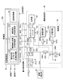
- FIG. 1 is a block diagram showing a configuration example of an AD converter with a self-calibration function according to the first embodiment of the present invention.
- the AD converter 100 with a self-calibration function shown in FIG. 1 is an AD converter that converts the input voltage into a digital value by comparing the integrated voltage and the input voltage generated by the charges sequentially accumulated in the capacitor Co with the comparator 34, and is a reference. It has at least two types of integration units, which are units of the voltage unit 10 and the amount of change in the integrated voltage of the capacitor Co. In the calibrated state, at least two types of integration units and the offset voltage of the comparator 34 are calibrated and converted.
- the integration conversion unit 30 that compares the input voltage and the integrated voltage to determine the digital value corresponding to the input voltage, and in the calibration state, the integration unit of the integration conversion unit 30 and the offset of the comparator 34 are offset by the calibration control unit 21. It is composed of a calibration control unit 21 that controls a process of calibrating a voltage and a control unit 20 having a conversion control unit 22 that controls a process of converting an input voltage into a digital value in a conversion state.
- the calibration control unit 21 determines the polarity of the offset voltage of the comparator 34 and measures the offset voltage.
- the polarity determination offset measurement processing unit 210 and the integration unit correlation measurement for deriving the relational expression of the correlation between the two types of integration units. It is composed of a processing unit 211 and an integration unit measurement processing unit 212 for measuring an integration unit.
- the integration conversion unit 30 has a sample hold unit 31 that holds an input value, has positive and negative inputs, determines that the positive input voltage exceeds the negative input voltage in the calibration state, and outputs a determination signal. Calibration with the comparer 34 and a crossbar switch 33 that switches the input to the comparer 34 to compare the sum and integrated voltage of the input voltage or reference voltage and the positive offset voltage of the comparer 34. In the state, the cross bar switch 33 and the reference voltage source are connected, and in the conversion state, the switching unit 32 that connects the sample hold unit 31 and the cross bar switch 33, the capacitor Co that generates an integrated voltage by the accumulated charge, and the capacitor.
- a positive current source 350 that stores an electric charge in Co
- a negative current source 351 that removes the electric charge accumulated in the capacitor Co
- a SW1 that connects and disconnects the capacitor Co and the positive current source 350
- It is composed of SW2 that connects and disconnects, SW3 that precharges the electric charge corresponding to the reference voltage to the capacitor Co, and SW4 that resets the electric charge accumulated in the capacitor Co.
- the integrating unit 35 is composed of SW1, SW2, SW4, a capacitor Co, a positive current source 350, and a negative current source 351.
- FIG. 2A shows an equivalent circuit model when s11 and s13 and s12 and s14 of the crossbar switch 33 are connected and a positive current source 350 and a capacitor Co are connected.
- the electrode connected to the current source side of the capacitor Co is positive (+), and the ground side is negative (-).
- the offset voltage of the comparator 34 is Vofc.
- FIG. 2B shows an equivalent circuit when s11 and s13 and s12 and s14 of the crossbar switch 33 are connected and a negative current source 351 and a capacitor Co are connected.
- the connection state of SW2 is repeated kn times, the charge (Co + Cp1) Vo, 0 before connecting the negative current source 351 and the capacitor Co is changed to In kn ⁇ t (In> 0) by the negative current source 351. Since the charge is removed, the integrated voltage is expressed by the following equation.
- the positive current source 350 can be used.
- the integrated voltage can be calculated from the number of times kp connected and the number of times kn connected to the negative current source 351.
- the integration unit at the time of connection to the positive current source 350 is described as the coarse adjustment positive integration unit
- the integration unit at the time of connection to the negative current source 351 is described as the fine adjustment negative integration unit.
- the offset voltage of the comparator 34 will be described as negative (Vofc ⁇ 0).
- the polarity determination offset measurement process, the integration unit correlation process, and the integration unit measurement process are performed with the a10 and b10 of the switching unit 32 connected.
- Each process of the calibration state is controlled by the polarity determination offset measurement processing unit 210, the integration unit correlation measurement processing unit 211, and the integration unit measurement processing unit 212.
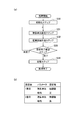
- FIG. 3 shows the processing flow in the polarity determination offset measurement processing unit 210, the integration unit, and the polarity setting table.
- SW1, SW2, and SW4 are disconnected, SW3 is connected, and s11 and s13 and s12 and s14 of the crossbar switch 33 are connected and s11.
- the comparison signal output from the comparator 34 is acquired in the state where s14 and s12 and s13 are connected, and the connected state of the crossbar switch 33 is set to the state where the low potential voltage is output. After that, the connection state of the crossbar switch 33 is not changed. Since Vofc ⁇ 0 for the sake of explanation, s11 and s13 and s12 and s14 are connected to the crossbar switch 33 after the completion of the polarity determination step S1.
- the integration unit is coarse adjustment and the polarity is positive.
- the number of integrations exceeds the reference voltage in the positive integration unit.
- the integration unit is fine adjustment and the polarity is negative.
- the number of integrations exceeding the reference voltage is measured in the negative integration unit.
- the integration unit 35 is controlled so as to read the first integration unit and polarity in the integration unit and polarity setting table and open / close only SW1.
- the process shifts to the integration count measurement process, and the integration is repeated until the integrated voltage ⁇ reference voltage + offset voltage is obtained based on the first polarity in the integration unit and polarity setting table.
- FIG. 4 shows the processing flow of the integration number measurement step S3.
- the magnitude relationship between the integrated voltage and the reference voltage + offset voltage is determined by the comparison signal output from the comparator 34.
- the offset voltage Vofc ⁇ 0 of the comparator 34 the sum of the reference voltage Vref and the offset voltage of the comparator 34 (Vref-Vofc in the equation because Vofc ⁇ 0) and the integrated voltage are input to the comparator 34, and the reference voltage is input.
- the comparator 34 outputs a low potential voltage comparison signal.
- the comparison signal becomes a high potential voltage, so that the comparison step of FIG. 4 can be processed.
- the integration unit 35 is set so as to be a fine adjustment negative integration unit. After the integration number measurement step S3 in the fine adjustment negative integration unit is completed, it is confirmed in the setting completion confirmation step S4 that there is no next setting in the integration unit and polarity setting table, and the process proceeds to the storage step S5.
- FIG. 5 shows an example of the relationship between the integrated voltage and the integrated number from the transition from the transition to the integrated number measurement step S3 to the transition to the storage step S5 for the first time in the polarity determination offset measurement process.
- VGp2 in equation (4) represents a coarse adjustment positive integration unit
- VGn1 in equation (5) represents a fine adjustment negative integration unit
- VGn1 ⁇ ko on the right side of the equation (3) represents the difference between the sum of the reference voltage and the offset voltage and the integrated voltage immediately before the storage step S5, and ⁇ ko is a real number of 0 or more and less than 1.
- FIG. 6 shows the processing flow in the integration unit correlation measurement processing unit 211 and the setting table of the integration unit and polarity.
- SW1, SW2, and SW4 are disconnected and SW3 is connected, and the capacitor Co is precharged with a charge corresponding to Vref (precharge step S20).
- the process proceeds to the excess coarse adjustment integration step S21, and the coarse adjustment positive integration unit is integrated by the number of integrations obtained by adding, for example, 2 to ko2 obtained by the polarity determination offset measurement process.
- the number to be added to ko2 may be any number as long as it is an integer of 1 or more.
- the subsequent processing is the same as the integration unit setting step S2 and subsequent processing of the polarity determination offset measurement processing. If the sum of the reference voltage and the offset voltage is equal to the sum of the reference voltage and the offset voltage at the kc + 1st time after the integration step is started for the first time in the integration unit correlation processing, kc is defined as the number of fine-tuning correlation integrations. In the storage step S24, kc is stored.
- VGn1 ⁇ kc on the right side of the equation (6) represents the difference between the sum of the reference voltage and the offset voltage and the integrated voltage immediately before the storage step S24, and ⁇ kc is a real number of 0 or more and less than 1.
- FIG. 7 shows the processing flow in the integration unit measurement processing unit 212.
- the integration unit measurement process is started, in the initialization step S30, SW1 to SW3 are disconnected, SW4 is connected and then disconnected, and the electric charge accumulated in the capacitor Co is reset.
- the subsequent processing is the same as the processing after the transition to the integration step for the first time in the polarity determination offset measurement processing. If the sum of the reference voltage and the offset voltage> the integrated voltage in the comparison step after the ki2 + 1th integration step, ki2 is defined as the number of coarse adjustment integrations.
- ki is defined as the number of fine adjustment integrations.
- ki2 and ki are stored.
- VGn1 ⁇ ki on the right side of the equation (7) represents the difference between the sum of the reference voltage and the offset voltage and the integrated voltage immediately before the storage step S34, and ⁇ ki is a real number of 0 or more and less than 1.
- ⁇ ki, ⁇ kc, and ⁇ ko contained in VGn1, VGp2, and Vofc are real numbers of 0 or more and less than 1, but their specific values are unknown. Due to the uncertainty of ⁇ ki, ⁇ kc, and ⁇ ko, the possible values of VGn1, VGp2, and Vofc have a range.
- the calibration value of VGn1, VGp2, and Vofc is determined by the median value in the range of VGn1, VGp2, and Vofc. The following equation is obtained by partially differentiating equation (10) with respect to ⁇ ki, ⁇ kc, and ⁇ ko.
- VGn1 increases monotonically with respect to ⁇ kc and decreases monotonically with respect to ⁇ ki and ⁇ ko. Therefore, the range of VGn1 is expressed by the following equation.
- the calibration value VGn1c of VGn1 can be obtained as shown in the following equation.
- VGp2 is monotonically increasing with respect to ⁇ ki and decreasing monotonically with respect to ⁇ ko.
- equation (20) if Ki> Ko, then ⁇ VGp2 / ⁇ ( ⁇ kc) ⁇ 0, and if Ki ⁇ Ko, then ⁇ VGp2 / ⁇ ( ⁇ kc)> 0. Therefore, in the case of Ki> Ko, VGp2 is monotonically decreasing with respect to ⁇ kc, and in the case of Ki ⁇ Ko, VGp2 is monotonically increasing with respect to ⁇ kc. From these relationships, the range of VGp2 in the case of Ki> Ko is given by the following equation, and by taking the median value, the calibration value VGp2c in the case of Ki> Ko becomes equation (22).
- Vofc is a monotonous decrease for ⁇ ki and a monotonous increase for ⁇ ko.
- equation (27) ⁇ Vofc / ⁇ ( ⁇ kc)> 0 in the case of (ko2 + 1) Ki> (ki2 + 1) Ko, and ⁇ Vofc in the case of (ko2 + 1) Ki ⁇ (ki2 + 1) Ko. / ⁇ ( ⁇ kc) ⁇ 0.
- the range of Vofc is given by equation (28), and by taking the median value, (ko2 + 1) Ki> (ki2 + 1) )
- the calibration value Vofcc in the case of Ko is given by Eq. (29).
- the integration units VGn1, VGp2 and the calibrated values of the offset voltage Vofc of the comparator VGn1c, VGp2c, Vofcc Can be obtained.
- FIG. 8 (a) shows an equivalent circuit model when the positive current source and the capacitor Co are connected with the cross bar switches 33 s11 and s14 and s12 and s13 connected.
- SW2 to SW4 are disconnected, SW1 is connected for a predetermined time ⁇ t, and then SW1 is disconnected repeatedly.
- the charge supplied from the positive current source is Ip kp ⁇ t.
- the integrated voltage is expressed by the following equation.
- FIG. 8B shows an equivalent circuit when s11 and s13 and s12 and s14 of the crossbar switch 33 are connected and a negative current source 351 and a capacitor Co are connected.
- the connection state of SW2 is repeated kn times, the charge (Co + Cp2) Vo, 0 before connecting the negative current source 351 and the capacitor Co is changed to In kn ⁇ t (In> 0) by the negative current source 351. Since the charge is removed, the integrated voltage is expressed by the following equation.
- the coarse adjustment offset integration number ko2 and the fine adjustment offset integration number ko are obtained from the processing flow of the polarity determination offset measurement processing unit 210 shown in FIG. From the equivalent circuit of FIG. 7, the positive input of the comparator is equivalently Vref + Vofc and the negative input is the integrated voltage. Therefore, the following relational expression holds for ko2 and ko and Vref, Vofc, VGn1, and VGp2. ..
- VGn1 ⁇ ko on the right side of equation (36) represents the difference between the sum of the reference voltage and offset voltage and the integrated voltage immediately before the storage step, and ⁇ ko is a real number greater than or equal to 0 and less than 1.
- the fine-tuned correlation integration number kc is obtained from the processing flow in the integration unit correlation measurement processing unit 211 shown in FIG.
- the following relational expressions hold for ko2 and kc, and for Vref, Vofc, VGn1, and VGp2.
- VGn1 ⁇ kc on the right side of the equation (37) represents the difference between the sum of the reference voltage and the offset voltage and the integrated voltage immediately before the storage step S34, and ⁇ kc is a real number of 0 or more and less than 1.
- the rough adjustment integration number ki2 and the fine adjustment integration number ki are obtained from the processing flow in the integration unit measurement processing unit shown in FIG.
- VGn1 ⁇ ki on the right side of the equation (38) represents the difference between the sum of the reference voltage and the offset voltage and the integrated voltage immediately before the storage step S34, and ⁇ ki is a real number of 0 or more and less than 1.
- Vofc has the same absolute value except for the sign.
- the calibration values of VGn1, VGp2, and Vofc are determined by the median of the range of VGn1, VGp2, and Vofc, as in the case of Vofc ⁇ 0. Since VGn1 when Vofc> 0 is the same as when Vofc ⁇ 0, the range of VGn1 is expressed by Eq. (16), and the calibration value VGn1c is Eq. (17). Similarly, for VGp2, the calibration value VGp2c when Vofc> 0 is Eq. (23) when Ki ⁇ Ko, and Eq. (24) when Ki> Ko.
- Vofc is a monotonous increase for ⁇ ki and a monotonous decrease for ⁇ ko.
- equation (43) ⁇ Vofc / ⁇ ( ⁇ kc) ⁇ 0 in the case of (ko2 + 1) Ki> (ki2 + 1) Ko, and ⁇ Vofc in the case of (ko2 + 1) Ki ⁇ (ki2 + 1) Ko. / ⁇ ( ⁇ kc)> 0.
- the range of Vofc is given by equation (44), and by taking the median value, (ko2 + 1) Ki> (ki2 + 1) )
- the calibration value Vofcc in the case of Ko is given by Eq. (45).
- FIG. 9 shows the processing flow of the conversion control unit 22 and the setting table of the integration unit and the polarity.
- the connection of the crossbar switch 33 based on the polarity of Vofc obtained by the polarity determination offset measurement process in the calibration state is maintained.
- a10 and c10 of the switching unit 32 are connected to hold the input voltage at the sample hold unit 31, and SW1 to SW3 are disconnected to reset the accumulated charge of the capacitor Co by connecting / disconnecting SW4. To do.
- the subsequent processing is the same as the integration unit measurement process except that the reference voltage of the integration unit measurement process becomes the input voltage.
- the coarse adjustment conversion integration number kv2 and the fine adjustment conversion integration number kv are obtained.
- the input voltage is Vin
- the following relational expression holds between kv2 and kv.
- Vofcc is different for Vofc ⁇ 0 and Vofc> 0, but considering the polarity of Vofc and the connection of the crossbar switch, it becomes
- the left side of 48) is Vin +
- VGn1c ⁇ kv on the right side of the equation (48) represents the difference between the sum of the input voltage and the offset voltage and the integrated voltage immediately before the storage step, and ⁇ kv is a real number of 0 or more and less than 1, but the specific value is unknown. Due to this uncertainty of ⁇ kv, the possible values of Vin have a range.
- the conversion value of Vin is determined by the median value of the Vin range.
- the range of Vin is given by the equation (49), and the converted value Vinc of Vin is expressed by the equation (50).
- the conversion value Vinc of the input voltage can be obtained by using the calibration values VGn1c, VGp2c, and Vofcc obtained in the calibration state.
- the offset of the comparator 34 and the capacity constituting the integration unit fluctuate due to aging
- the offset of the comparator 34 and the integration unit 35 which is the analog value output unit of the DA converter It is possible to provide an AD converter that can be calibrated and has high long-term stability.
- the integrated voltage can be integrated with a reference voltage or input voltage with a small number of integrations and with high accuracy as compared with the case of integrating with only a small integration unit. Can be accumulated up to.
- the calibration process and the conversion process can be performed with a small number of integrations and with high accuracy as compared with the case where the integration processing is performed only in a small integration unit.
- FIG. 10 shows a modified example of the first embodiment.
- the integration unit 55 using the variable positive current source 550 and the variable negative current source 551 and the calibration control unit 41 are subjected to multiple integration unit measurement processing. It differs in that part 410 is added. Further, the processing flow of the conversion control unit 42 is different.
- the variable positive current source 550 generates two types of integration units, a coarse adjustment positive integration unit and a fine adjustment positive integration unit that increase the integrated voltage, and a coarse adjustment positive integration unit and a fine adjustment positive integration unit are generated by the signal MAGP from the control unit. The current that produces is set.
- the variable negative current source 551 generates two types of integration units, a coarse adjustment negative integration unit and a fine adjustment negative integration unit that reduce the integrated voltage, and a coarse adjustment negative integration unit and a fine adjustment negative integration unit are generated by the signal MAGN from the control unit 40. The current that produces the unit is set.
- the coarse adjustment positive integration unit is VGp2
- the fine adjustment positive integration unit is VGp1
- the coarse adjustment negative integration unit is VGn2
- the fine adjustment negative integration unit is VGn1.
- the polarity determination offset measurement processing unit 210, the integration unit correlation measurement processing unit 211, the multiple integration unit measurement processing unit 410, and the integration unit measurement processing unit 212 of the calibration control unit 41 perform polarity determination offset measurement processing and integration, respectively. Carry out unit correlation processing, multiple integration unit measurement processing, and integration unit measurement processing.
- variable positive current source 550 set to generate the coarse adjustment positive integration unit VGp2 and the variable negative current source 551 to generate the fine adjustment negative integration unit VG1n
- the polarity determination offset measurement process and the integration unit correlation Carry out the measurement process. Since these processes are the same as in FIG. 1, they are omitted.
- Vofc when Vofc ⁇ 0, the relational expression between Eqs. (3) and (6) is established, and when Vofc> 0, the relational expression between Eqs. (36) and (37) is satisfied.
- the number of integrations ko2, the number of fine adjustment offset integrations ko, and the number of fine adjustment correlation integrations kc can be obtained.
- FIG. 11 shows the processing flow of the multiple integration unit measurement processing unit 410.
- SW1, SW2, and SW4 are disconnected, SW3 is connected, the capacitor Co is precharged, and the initial value of the integrated voltage is set as the reference voltage Vref (step S50).
- SW3 is disconnected, and in the first integration step S51, a variable positive current source is set to generate a coarse adjustment negative integration unit VGn2, and S is connected and disconnected from SW2 a predetermined number of times predetermined times to integrate. Remove ke2 VGn2 from the voltage.
- the same processing as after the integration unit setting step of the polarity determination offset measurement processing is performed.
- ke2 is defined as the second coarse adjustment negative coefficient integration number. Assuming that the sum of the reference voltage and the offset voltage is equal to the integrated voltage in the ke + 1st integration step after setting the fine adjustment negative integration unit, ke is defined as the first coarse adjustment negative coefficient integration number.
- ke is stored. For ke, the following equation holds when Vofc ⁇ 0.
- VGn1 ⁇ ke on the right side represents the difference between the sum of the reference voltage and offset voltage and the integrated voltage immediately before the storage step, and ⁇ ke is a real number of 0 or more and less than 1.
- the integration unit measurement process is performed in a state where the variable positive current source 550 is set to generate the coarse adjustment positive integration unit VGp2, and the variable negative current source 551 is set to generate the fine adjustment negative integration unit VG1n. Since this process is the same as in FIG. 1, it is omitted.
- Vofc when Vofc ⁇ 0, the relational expression of Eq. (7) is established, and when Vofc> 0, the rough adjustment integration number ki2 and the fine adjustment integration number ki, for which the relational expression of Eq. (38) is satisfied, are obtained. ..
- ⁇ kc, ⁇ ko, ⁇ ke contained in VGn2 are real numbers of 0 or more and less than 1, but the specific values are unknown. Due to the uncertainty of ⁇ kc, ⁇ ko, and ⁇ ke, the possible values of VGn2 have a range.
- the calibration value of VGn2 is determined by the median value of the range of VGn2.
- the calibration value VGn1c is used for VGn1.
- the following equation is obtained by partially differentiating equation (53) with respect to ⁇ kc, ⁇ ko, and ⁇ ke.
- VGn1c ⁇ 0, kp2> ko2 was used to derive the inequality sign in the above equation. From equations (54) to (56), VGn2 is monotonically increasing with respect to ⁇ ke and ⁇ ko and monotonically decreasing with respect to ⁇ kc. Therefore, the range of VGn2 is given by the equation (57), and the calibration value VGn2c is expressed by the equation (58) by taking the median value.
- the polarity determination offset measurement processing, integration unit correlation processing, multiple integration unit measurement processing, and integration unit measurement processing in the calibration state are used to calibrate the integration units VGn1, VGp2, VGn2 and the offset voltage Vofc of the comparator.
- the values VGn1c, VGp2c, VGn2c and Vofcc can be obtained.
- FIG. 12 shows the processing flow of the conversion control unit that is executed in the conversion state.
- the connection of the crossbar switch 33 based on the polarity of Vofc obtained by the polarity determination offset measurement process in the calibration state is maintained.
- the processing of the conversion control unit 42 is started, in the reference voltage comparison step S60, a10 and c10 of the switching unit 32 are connected, the input voltage is held by the sample holding unit 31, and SW1, SW2, and SW4 are disconnected. By connecting SW3, the capacitor Co is precharged with a charge corresponding to the reference voltage. After that, the input voltage held by the sample hold unit 31 and the reference voltage are compared by the comparator 34, and the SW3 is disconnected. If the input voltage is larger, the process proceeds to the setting table 1 reading step S61, and if the input voltage is smaller, the process proceeds to the setting table 2 reading step S62. In the following, as an example, the case where the input voltage is small will be described.
- the coarse adjustment negative is the number of integrations in the integration unit and polarity setting table 2.
- the conversion integration number kvn2 the coarse adjustment positive conversion integration number kv2 which is the integration number in the coarse adjustment positive integration unit
- the fine adjustment negative conversion integration number kv which is the integration number in the fine adjustment negative integration unit
- Vofcc is different for Vofc ⁇ 0 and Vofc> 0, but considering the polarity of Vofc and the connection of the crossbar switch, the formula is
- VGn1c ⁇ kv on the right side of the equation (59) represents the difference between the sum of the input voltage and the offset voltage and the integrated voltage immediately before the storage step, and ⁇ kv is a real number of 0 or more and less than 1, but the specific value is unknown. Due to this uncertainty of ⁇ kv, the possible values of Vin have a range. The conversion value of Vin is determined by the median value of the Vin range. The conversion value Vinc of Vin is expressed by the equation (60).
- the integration unit and polarity setting table 1 is read, so that kv2 and kv can be obtained by the processing up to the storage step.
- the conversion value of Vin in this case is the same as that in the equation (50).
- the conversion value Vinc of the input voltage can be obtained by using the calibration values VGn1c, VGp2c, VGn2c, and Vofcc obtained in the calibration state.
- the offset of the comparator 34 and the capacity constituting the integration unit fluctuate due to aging
- the offset of the comparator 34 and the integration unit 55 which is an analog value output unit of the DA converter It is possible to provide an AD converter that can be calibrated and has high long-term stability.
- FIG. 13 shows a block diagram of the AD converter according to the second embodiment of the present invention.
- the AD converter 300 with a self-calibration function shown in FIG. 13 is composed of N conversion units 1 to N, a parallel processing control unit 60, and a reference voltage unit 10.
- the control unit 20 * and the integration conversion unit 30 * of the individual conversion units are the same as the control unit 40 * and the integration conversion unit 50 * of the first embodiment or the modified example, respectively.
- the operation control / comparison signal inside the conversion unit represents a bundle of signals including both the operation control signal and the comparison signal of the first embodiment or the modified example.
- the parallel processing control unit 60 controls the processing of the control unit of each conversion unit by the setting data, and receives the conversion data including the calibration value of the integration unit and the offset voltage and the digital value of the input voltage from the conversion unit that has executed the conversion processing. Then, the input voltage calibrated from the digital value included in the conversion data is output as parallel processing conversion data.
- FIG. 14 shows a diagram illustrating the processing state of each unit in this case.
- the parallel processing control unit 60 receives the parallel setting data including the instruction to start the processing, the parallel processing control unit 60 transmits the setting data including the instruction to start the polarity determination offset measurement processing to the conversion unit 1.
- the conversion unit 1 starts the polarity determination offset measurement process.
- the parallel processing control unit 60 transmits setting data including an instruction to start the integration unit correlation processing to the conversion unit 1, and includes an instruction to start the polarity determination offset measurement processing to the conversion unit 2.
- the conversion unit 1 starts the integration unit correlation process
- the conversion unit 2 starts the polarity determination offset measurement process.
- each conversion unit shifts one process by one to perform calibration state processing and conversion processing, so that each conversion unit performs calibration and conversion in sequence, and in any one conversion unit, It is possible to both carry out the conversion process. Therefore, the conversion process can be continuously performed in units of one process using the conversion unit that has been calibrated at all times.
- the AD converter 300 with a self-calibration function calibrates the conversion units 1 to N in which N of the above-mentioned AD converters 100 and 200 with a self-calibration function are arranged, and the conversion units 1 to N. It is provided with a parallel processing control unit 60 that controls so that the operation of calibrating each of the AD converters 100 and 200 with a calibration function and the operation of converting an input voltage into a digital signal are not synchronized. As a result, the AD converter 300 with a self-calibration function can operate at high speed.
- the AD converter 100 with a self-calibration function described above is an AD converter with a self-calibration function that does not require a measuring instrument for calibration, and has a calibration control unit 21 that controls the operation of calibrating itself and an input voltage to be converted.
- a control unit 20 including a conversion control unit 22 that controls an operation of converting a digital signal into a digital signal, a reference voltage unit 10 that outputs a reference voltage, and an integration unit 35 that generates an integrated voltage obtained by integrating two or more unit voltages.
- a comparator 34 that has two inputs and compares the integrated voltage with the input voltage or reference voltage, and inputs the integrated voltage to one input of the comparator 34 and inputs the input voltage or reference voltage to the other input.
- It includes an integration conversion unit including a cross bar switch 33 for switching a connection between a case and a case where an input voltage or a reference voltage is input to one input of the comparator 34 and an integrated voltage is input to the other input.
- the calibration control unit 21 crosses the input reference voltage and the integrated voltage of the comparator 34 so that the low potential voltage is output to the output of the comparator 34 after the integrated voltage is precharged with the reference voltage.
- the polarity determination offset measurement processing unit 210 which switches with the bar switch 33 to determine the polarity of the offset voltage of the comparator 34, obtains the number of integrations at which the integrated voltage becomes the reference voltage, and measures the offset voltage of the comparator 34, and the integrated. After discharging the voltage, the comparator 34 is made to compare the reference voltage and the integrated voltage, and the integrated unit measurement processing unit 211 that measures the integrated unit from the integrated number of times when the integrated voltage exceeding the reference voltage is obtained, and the polarity determination offset.
- the integration unit correlation measurement unit 211 that derives the correlation equation between two types of integration units using the integration voltage obtained by adding an integer of 1 or more to the integration number obtained by the measurement processing unit 210 and integrating the unit voltage. To be equipped. As a result, the integration units VGn1 and VGp2 and the calibration values of the offset voltage Vofc of the comparator, VGn1c, VGp2c and Vofcc, can be obtained.
- the polarity determination offset measurement processing unit 210 determines the polarity of the offset voltage of the comparator 34, and if the polarity is positive, the integration voltage obtained by integrating the coarse adjustment positive integration unit having a positive polarity on the integration unit 35 is obtained. , The first integration number exceeding the reference voltage is measured, and then the fine adjustment negative integration unit whose absolute value is smaller than the coarse adjustment positive integration unit whose polarity is negative is integrated, and the integrated voltage exceeds the reference voltage. The number of times is measured, and if the polarity is negative, the integrated voltage obtained by integrating the coarse adjustment negative integration unit having a negative polarity on the integrating unit 35 measures the first integrated number of times exceeding the reference voltage, and then the polarity is positive.
- the second integration number in which the integrated voltage obtained by integrating the fine adjustment positive integration unit whose absolute value is smaller than the coarse adjustment positive integration unit exceeds the reference voltage is measured.
- the integrated voltage can be integrated up to the reference voltage or the input voltage with a small number of integrations and with high accuracy as compared with the case of integrating with only a small integration unit.
- the AD converters 100, 200, and 300 with a self-calibration function according to the present embodiment do not require a measuring instrument for calibration and can calibrate themselves by remote control. Therefore, the AD converter with a self-calibration function of the present invention is suitable for use in combination with a large number of sensors in remote locations.
- AD converter with self-calibration function 10 Reference voltage unit 20, 40: Control unit 21, 41: Calibration control unit 22, 42: Conversion control unit 30, 50: Integration conversion unit 31: Sample hold unit 32 : Switching unit 33: Cross bar switch 34: Comparator 35, 55: Integration unit 60: Parallel processing control unit 210: Polarity determination offset measurement processing unit 211: Integration unit correlation measurement processing unit 212: Integration unit measurement processing unit 350: Positive current source 351: Negative current source 410: Multiple integration unit measurement processing unit 550: Variable positive current source 551: Variable negative current source
Abstract
L'invention concerne un convertisseur A/N ayant une fonction d'auto-correction pour laquelle aucun équipement de mesure pour la correction d'épreuves n'est nécessaire. Un convertisseur A/N ayant une fonction d'auto-correction pour laquelle aucun équipement de mesure pour la correction d'épreuves n'est requis est pourvu de : une unité de commande 20 comprenant une unité de commande de correction d'épreuve 21 pour commander une opération d'auto-correction d'épreuve et une unité de commande de conversion 22 pour commander une opération de conversion d'une tension d'entrée, qui doit être convertie en un signal numérique ; une unité de tension de référence 10 pour délivrer une tension de référence ; et une unité de conversion d'intégration 30 comprenant une unité d'intégration 35 pour générer une tension intégrée obtenue par intégration de deux types ou plus de tensions unitaires, un comparateur 34 ayant deux entrées pour comparer la tension intégrée à une tension d'entrée ou à la tension de référence, et un commutateur crossbar 33 pour commuter des connexions entre un cas d'entrée de la tension intégrée à une entrée du comparateur 34 et l'entrée de la tension d'entrée ou de la tension de référence à l'autre entrée et un cas d'entrée de la tension d'entrée ou de la tension de référence à une entrée du comparateur 34 et l'entrée de la tension intégrée à l'autre entrée.
Priority Applications (3)
| Application Number | Priority Date | Filing Date | Title |
|---|---|---|---|
| US17/608,106 US11770127B2 (en) | 2019-05-21 | 2019-05-21 | Self-calibration function-equipped AD converter |
| JP2021519937A JP7315868B2 (ja) | 2019-05-21 | 2019-05-21 | 自己校正機能付きadコンバータ |
| PCT/JP2019/020097 WO2020234995A1 (fr) | 2019-05-21 | 2019-05-21 | Convertisseur a/n à fonction d'auto-correction |
Applications Claiming Priority (1)
| Application Number | Priority Date | Filing Date | Title |
|---|---|---|---|
| PCT/JP2019/020097 WO2020234995A1 (fr) | 2019-05-21 | 2019-05-21 | Convertisseur a/n à fonction d'auto-correction |
Publications (1)
| Publication Number | Publication Date |
|---|---|
| WO2020234995A1 true WO2020234995A1 (fr) | 2020-11-26 |
Family
ID=73459080
Family Applications (1)
| Application Number | Title | Priority Date | Filing Date |
|---|---|---|---|
| PCT/JP2019/020097 WO2020234995A1 (fr) | 2019-05-21 | 2019-05-21 | Convertisseur a/n à fonction d'auto-correction |
Country Status (3)
| Country | Link |
|---|---|
| US (1) | US11770127B2 (fr) |
| JP (1) | JP7315868B2 (fr) |
| WO (1) | WO2020234995A1 (fr) |
Cited By (1)
| Publication number | Priority date | Publication date | Assignee | Title |
|---|---|---|---|---|
| WO2022264307A1 (fr) * | 2021-06-16 | 2022-12-22 | 日本電信電話株式会社 | Convertisseur an équipé d'une fonction d'auto-étalonnage |
Families Citing this family (1)
| Publication number | Priority date | Publication date | Assignee | Title |
|---|---|---|---|---|
| US11714437B2 (en) * | 2019-05-28 | 2023-08-01 | Nippon Telegraph And Telephone Corporation | Variable reference voltage source |
Citations (2)
| Publication number | Priority date | Publication date | Assignee | Title |
|---|---|---|---|---|
| JPH0575465A (ja) * | 1991-09-12 | 1993-03-26 | Hitachi Ltd | フイールド機器用a/d変換器 |
| US20050197796A1 (en) * | 2004-08-16 | 2005-09-08 | Daigle Clayton H. | Calibrating analog-to-digital systems using a precision reference and a pulse-width modulation circuit to reduce local and large signal nonlinearities |
Family Cites Families (7)
| Publication number | Priority date | Publication date | Assignee | Title |
|---|---|---|---|---|
| US5117227A (en) * | 1991-09-27 | 1992-05-26 | Hewlett-Packard Company | Continuously integrating high-resolution analog-to-digital converter |
| JP2010010921A (ja) * | 2008-06-25 | 2010-01-14 | Fujitsu Ltd | Ad変換装置及びad変換方法 |
| JP2010199799A (ja) * | 2009-02-24 | 2010-09-09 | Renesas Electronics Corp | アナログデジタル変換回路 |
| EP2629428A1 (fr) * | 2012-02-16 | 2013-08-21 | Imec | Convertisseur analogique/numérique et son procédé d'étalonnage |
| JP6243281B2 (ja) * | 2014-04-15 | 2017-12-06 | 日本電信電話株式会社 | センサ回路 |
| JP7079914B2 (ja) * | 2018-11-12 | 2022-06-03 | 日本電信電話株式会社 | 自己校正機能付きadコンバータ |
| JP7089182B2 (ja) * | 2018-11-19 | 2022-06-22 | 日本電信電話株式会社 | 可変基準電圧源 |
-
2019
- 2019-05-21 US US17/608,106 patent/US11770127B2/en active Active
- 2019-05-21 WO PCT/JP2019/020097 patent/WO2020234995A1/fr active Application Filing
- 2019-05-21 JP JP2021519937A patent/JP7315868B2/ja active Active
Patent Citations (2)
| Publication number | Priority date | Publication date | Assignee | Title |
|---|---|---|---|---|
| JPH0575465A (ja) * | 1991-09-12 | 1993-03-26 | Hitachi Ltd | フイールド機器用a/d変換器 |
| US20050197796A1 (en) * | 2004-08-16 | 2005-09-08 | Daigle Clayton H. | Calibrating analog-to-digital systems using a precision reference and a pulse-width modulation circuit to reduce local and large signal nonlinearities |
Cited By (1)
| Publication number | Priority date | Publication date | Assignee | Title |
|---|---|---|---|---|
| WO2022264307A1 (fr) * | 2021-06-16 | 2022-12-22 | 日本電信電話株式会社 | Convertisseur an équipé d'une fonction d'auto-étalonnage |
Also Published As
| Publication number | Publication date |
|---|---|
| JP7315868B2 (ja) | 2023-07-27 |
| JPWO2020234995A1 (fr) | 2020-11-26 |
| US20220337262A1 (en) | 2022-10-20 |
| US11770127B2 (en) | 2023-09-26 |
Similar Documents
| Publication | Publication Date | Title |
|---|---|---|
| US9407839B2 (en) | Solid-state imaging device | |
| JP7079914B2 (ja) | 自己校正機能付きadコンバータ | |
| US20130044014A1 (en) | Successive approximation analog to digital converter with capacitor mismatch calibration and method thereof | |
| US20120194367A1 (en) | Continuous ramp generator design and its calibration for cmos image sensors using single-ramp adcs | |
| WO2009136630A1 (fr) | Dispositif de capteur | |
| US9191018B2 (en) | Analog-digital converter | |
| US10128861B2 (en) | Analog to digital conversion circuit | |
| WO2020234995A1 (fr) | Convertisseur a/n à fonction d'auto-correction | |
| JP7239863B2 (ja) | 自己校正機能付きadコンバータ | |
| EP1398880A2 (fr) | Circuit de conversion analogique-numérique | |
| JP2013150117A (ja) | アナログデジタル変換器および受信機 | |
| US9823285B2 (en) | Charge measurement | |
| JP2002124877A (ja) | A/d変換装置および固体撮像装置 | |
| JP7089182B2 (ja) | 可変基準電圧源 | |
| WO2022264307A1 (fr) | Convertisseur an équipé d'une fonction d'auto-étalonnage | |
| JP7406168B2 (ja) | 自己校正機能付きadコンバータ | |
| JP7125648B2 (ja) | 可変基準電圧源 | |
| JP5763558B2 (ja) | 測定装置及びそれを用いた測定方法 | |
| JP2014039218A (ja) | Ad変換器 |
Legal Events
| Date | Code | Title | Description |
|---|---|---|---|
| 121 | Ep: the epo has been informed by wipo that ep was designated in this application |
Ref document number: 19929675 Country of ref document: EP Kind code of ref document: A1 |
|
| ENP | Entry into the national phase |
Ref document number: 2021519937 Country of ref document: JP Kind code of ref document: A |
|
| NENP | Non-entry into the national phase |
Ref country code: DE |
|
| 122 | Ep: pct application non-entry in european phase |
Ref document number: 19929675 Country of ref document: EP Kind code of ref document: A1 |