WO2020234995A1 - A/d converter with self-proofreading function - Google Patents
A/d converter with self-proofreading function Download PDFInfo
- Publication number
- WO2020234995A1 WO2020234995A1 PCT/JP2019/020097 JP2019020097W WO2020234995A1 WO 2020234995 A1 WO2020234995 A1 WO 2020234995A1 JP 2019020097 W JP2019020097 W JP 2019020097W WO 2020234995 A1 WO2020234995 A1 WO 2020234995A1
- Authority
- WO
- WIPO (PCT)
- Prior art keywords
- voltage
- unit
- integration
- input
- reference voltage
- Prior art date
Links
Images


Classifications
-
- H—ELECTRICITY
- H03—ELECTRONIC CIRCUITRY
- H03M—CODING; DECODING; CODE CONVERSION IN GENERAL
- H03M1/00—Analogue/digital conversion; Digital/analogue conversion
- H03M1/10—Calibration or testing
- H03M1/1009—Calibration
- H03M1/1014—Calibration at one point of the transfer characteristic, i.e. by adjusting a single reference value, e.g. bias or gain error
- H03M1/1023—Offset correction
-
- H—ELECTRICITY
- H03—ELECTRONIC CIRCUITRY
- H03M—CODING; DECODING; CODE CONVERSION IN GENERAL
- H03M1/00—Analogue/digital conversion; Digital/analogue conversion
- H03M1/10—Calibration or testing
-
- H—ELECTRICITY
- H03—ELECTRONIC CIRCUITRY
- H03M—CODING; DECODING; CODE CONVERSION IN GENERAL
- H03M1/00—Analogue/digital conversion; Digital/analogue conversion
- H03M1/12—Analogue/digital converters
- H03M1/50—Analogue/digital converters with intermediate conversion to time interval
- H03M1/56—Input signal compared with linear ramp
Definitions
- the present invention relates to an AD converter with a self-calibration function that does not require a measuring instrument for calibration.
- the AD converter consists of a DA converter that outputs a known voltage and a comparator, and the smallest DA converter that sequentially changes the output value of the DA converter and changes the output of the comparator from a low output voltage to a high output voltage.
- the digital value when the output value of is set is used as the conversion value of the AD converter (Non-Patent Document 1). Fluctuations due to the offset and linearity of the DA converter over time lead to changes over time of the AD converter.
- Typical DA converters include an R-2R ladder circuit, a resistance string circuit (Non-Patent Document 2), and a PWM circuit (Non-Patent Document 3).
- R-2R ladder circuit a variable signal source with high resolution and high accuracy can be configured with a relatively small number of resistance elements.
- a resistor with high accuracy is required on the MSB side.
- the resistance string circuit has low power consumption and high monotonous increase, but since the linearity of the output with respect to the setting code depends on the uniformity of the resistance element and the layout, trial and error of layout design and manufacturing is required.
- the PWM circuit has the advantage of stable performance because it does not require a resistor element sequence and can be manufactured only with a digital circuit, but it is high for removing ripple noise that appears in the output.
- the next low-pass filter needs to be designed and manufactured with high frequency accuracy.
- Non-Patent Document 2 the offset voltage of the comparator, the unit voltage of the DA converter and its linearity change over time. Therefore, in order to maintain the conversion accuracy for a long period of time, periodic calibration is indispensable (Non-Patent Document 2).
- the present invention has been made in view of this problem, and an object of the present invention is to provide an AD converter with a self-calibration function that does not require a measuring instrument for calibration.
- the AD converter with a self-calibration function is an AD converter with a self-calibration function that does not require a measuring instrument for calibration, and is a calibration control unit that controls the operation of calibrating itself and a conversion target.
- a control unit that includes a conversion control unit that controls the operation of converting an input voltage into a digital signal, a reference voltage unit that outputs a reference voltage, an integration unit that generates an integrated voltage that integrates two or more unit voltages, and an input.
- a comparator that compares the integrated voltage with the input voltage or the reference voltage, and the integrated voltage is input to one input of the comparator and the input voltage or the reference voltage is input to the other input.
- An integration converter including a cross bar switch that switches the connection between the case of inputting the input voltage and the case of inputting the input voltage or the reference voltage to one input of the comparator and inputting the integrated voltage to the other input.
- the gist is to have.
- FIG. 1 It is a functional block diagram which shows the structural example of the AD compactor with self-calibration function which concerns on 1st Embodiment of this invention. It is a figure which shows the equivalent circuit of the integration part shown in FIG. It is a flowchart which shows the processing procedure of the polarity determination offset measurement processing unit shown in FIG. It is a flowchart which shows the processing procedure of the integration number measurement step. It is a figure which shows typically the relationship between the integration number of times and the integration voltage. It is a flowchart which shows the processing procedure of the integration unit correlation measurement processing unit shown in FIG. It is a flowchart which shows the processing procedure of the integration unit measurement processing unit shown in FIG. It is a figure which shows the other equivalent circuit of the integration part shown in FIG.
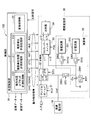
- FIG. 1 is a block diagram showing a configuration example of an AD converter with a self-calibration function according to the first embodiment of the present invention.
- the AD converter 100 with a self-calibration function shown in FIG. 1 is an AD converter that converts the input voltage into a digital value by comparing the integrated voltage and the input voltage generated by the charges sequentially accumulated in the capacitor Co with the comparator 34, and is a reference. It has at least two types of integration units, which are units of the voltage unit 10 and the amount of change in the integrated voltage of the capacitor Co. In the calibrated state, at least two types of integration units and the offset voltage of the comparator 34 are calibrated and converted.
- the integration conversion unit 30 that compares the input voltage and the integrated voltage to determine the digital value corresponding to the input voltage, and in the calibration state, the integration unit of the integration conversion unit 30 and the offset of the comparator 34 are offset by the calibration control unit 21. It is composed of a calibration control unit 21 that controls a process of calibrating a voltage and a control unit 20 having a conversion control unit 22 that controls a process of converting an input voltage into a digital value in a conversion state.
- the calibration control unit 21 determines the polarity of the offset voltage of the comparator 34 and measures the offset voltage.
- the polarity determination offset measurement processing unit 210 and the integration unit correlation measurement for deriving the relational expression of the correlation between the two types of integration units. It is composed of a processing unit 211 and an integration unit measurement processing unit 212 for measuring an integration unit.
- the integration conversion unit 30 has a sample hold unit 31 that holds an input value, has positive and negative inputs, determines that the positive input voltage exceeds the negative input voltage in the calibration state, and outputs a determination signal. Calibration with the comparer 34 and a crossbar switch 33 that switches the input to the comparer 34 to compare the sum and integrated voltage of the input voltage or reference voltage and the positive offset voltage of the comparer 34. In the state, the cross bar switch 33 and the reference voltage source are connected, and in the conversion state, the switching unit 32 that connects the sample hold unit 31 and the cross bar switch 33, the capacitor Co that generates an integrated voltage by the accumulated charge, and the capacitor.
- a positive current source 350 that stores an electric charge in Co
- a negative current source 351 that removes the electric charge accumulated in the capacitor Co
- a SW1 that connects and disconnects the capacitor Co and the positive current source 350
- It is composed of SW2 that connects and disconnects, SW3 that precharges the electric charge corresponding to the reference voltage to the capacitor Co, and SW4 that resets the electric charge accumulated in the capacitor Co.
- the integrating unit 35 is composed of SW1, SW2, SW4, a capacitor Co, a positive current source 350, and a negative current source 351.
- FIG. 2A shows an equivalent circuit model when s11 and s13 and s12 and s14 of the crossbar switch 33 are connected and a positive current source 350 and a capacitor Co are connected.
- the electrode connected to the current source side of the capacitor Co is positive (+), and the ground side is negative (-).
- the offset voltage of the comparator 34 is Vofc.
- FIG. 2B shows an equivalent circuit when s11 and s13 and s12 and s14 of the crossbar switch 33 are connected and a negative current source 351 and a capacitor Co are connected.
- the connection state of SW2 is repeated kn times, the charge (Co + Cp1) Vo, 0 before connecting the negative current source 351 and the capacitor Co is changed to In kn ⁇ t (In> 0) by the negative current source 351. Since the charge is removed, the integrated voltage is expressed by the following equation.
- the positive current source 350 can be used.
- the integrated voltage can be calculated from the number of times kp connected and the number of times kn connected to the negative current source 351.
- the integration unit at the time of connection to the positive current source 350 is described as the coarse adjustment positive integration unit
- the integration unit at the time of connection to the negative current source 351 is described as the fine adjustment negative integration unit.
- the offset voltage of the comparator 34 will be described as negative (Vofc ⁇ 0).
- the polarity determination offset measurement process, the integration unit correlation process, and the integration unit measurement process are performed with the a10 and b10 of the switching unit 32 connected.
- Each process of the calibration state is controlled by the polarity determination offset measurement processing unit 210, the integration unit correlation measurement processing unit 211, and the integration unit measurement processing unit 212.
- FIG. 3 shows the processing flow in the polarity determination offset measurement processing unit 210, the integration unit, and the polarity setting table.
- SW1, SW2, and SW4 are disconnected, SW3 is connected, and s11 and s13 and s12 and s14 of the crossbar switch 33 are connected and s11.
- the comparison signal output from the comparator 34 is acquired in the state where s14 and s12 and s13 are connected, and the connected state of the crossbar switch 33 is set to the state where the low potential voltage is output. After that, the connection state of the crossbar switch 33 is not changed. Since Vofc ⁇ 0 for the sake of explanation, s11 and s13 and s12 and s14 are connected to the crossbar switch 33 after the completion of the polarity determination step S1.
- the integration unit is coarse adjustment and the polarity is positive.
- the number of integrations exceeds the reference voltage in the positive integration unit.
- the integration unit is fine adjustment and the polarity is negative.
- the number of integrations exceeding the reference voltage is measured in the negative integration unit.
- the integration unit 35 is controlled so as to read the first integration unit and polarity in the integration unit and polarity setting table and open / close only SW1.
- the process shifts to the integration count measurement process, and the integration is repeated until the integrated voltage ⁇ reference voltage + offset voltage is obtained based on the first polarity in the integration unit and polarity setting table.
- FIG. 4 shows the processing flow of the integration number measurement step S3.
- the magnitude relationship between the integrated voltage and the reference voltage + offset voltage is determined by the comparison signal output from the comparator 34.
- the offset voltage Vofc ⁇ 0 of the comparator 34 the sum of the reference voltage Vref and the offset voltage of the comparator 34 (Vref-Vofc in the equation because Vofc ⁇ 0) and the integrated voltage are input to the comparator 34, and the reference voltage is input.
- the comparator 34 outputs a low potential voltage comparison signal.
- the comparison signal becomes a high potential voltage, so that the comparison step of FIG. 4 can be processed.
- the integration unit 35 is set so as to be a fine adjustment negative integration unit. After the integration number measurement step S3 in the fine adjustment negative integration unit is completed, it is confirmed in the setting completion confirmation step S4 that there is no next setting in the integration unit and polarity setting table, and the process proceeds to the storage step S5.
- FIG. 5 shows an example of the relationship between the integrated voltage and the integrated number from the transition from the transition to the integrated number measurement step S3 to the transition to the storage step S5 for the first time in the polarity determination offset measurement process.
- VGp2 in equation (4) represents a coarse adjustment positive integration unit
- VGn1 in equation (5) represents a fine adjustment negative integration unit
- VGn1 ⁇ ko on the right side of the equation (3) represents the difference between the sum of the reference voltage and the offset voltage and the integrated voltage immediately before the storage step S5, and ⁇ ko is a real number of 0 or more and less than 1.
- FIG. 6 shows the processing flow in the integration unit correlation measurement processing unit 211 and the setting table of the integration unit and polarity.
- SW1, SW2, and SW4 are disconnected and SW3 is connected, and the capacitor Co is precharged with a charge corresponding to Vref (precharge step S20).
- the process proceeds to the excess coarse adjustment integration step S21, and the coarse adjustment positive integration unit is integrated by the number of integrations obtained by adding, for example, 2 to ko2 obtained by the polarity determination offset measurement process.
- the number to be added to ko2 may be any number as long as it is an integer of 1 or more.
- the subsequent processing is the same as the integration unit setting step S2 and subsequent processing of the polarity determination offset measurement processing. If the sum of the reference voltage and the offset voltage is equal to the sum of the reference voltage and the offset voltage at the kc + 1st time after the integration step is started for the first time in the integration unit correlation processing, kc is defined as the number of fine-tuning correlation integrations. In the storage step S24, kc is stored.
- VGn1 ⁇ kc on the right side of the equation (6) represents the difference between the sum of the reference voltage and the offset voltage and the integrated voltage immediately before the storage step S24, and ⁇ kc is a real number of 0 or more and less than 1.
- FIG. 7 shows the processing flow in the integration unit measurement processing unit 212.
- the integration unit measurement process is started, in the initialization step S30, SW1 to SW3 are disconnected, SW4 is connected and then disconnected, and the electric charge accumulated in the capacitor Co is reset.
- the subsequent processing is the same as the processing after the transition to the integration step for the first time in the polarity determination offset measurement processing. If the sum of the reference voltage and the offset voltage> the integrated voltage in the comparison step after the ki2 + 1th integration step, ki2 is defined as the number of coarse adjustment integrations.
- ki is defined as the number of fine adjustment integrations.
- ki2 and ki are stored.
- VGn1 ⁇ ki on the right side of the equation (7) represents the difference between the sum of the reference voltage and the offset voltage and the integrated voltage immediately before the storage step S34, and ⁇ ki is a real number of 0 or more and less than 1.
- ⁇ ki, ⁇ kc, and ⁇ ko contained in VGn1, VGp2, and Vofc are real numbers of 0 or more and less than 1, but their specific values are unknown. Due to the uncertainty of ⁇ ki, ⁇ kc, and ⁇ ko, the possible values of VGn1, VGp2, and Vofc have a range.
- the calibration value of VGn1, VGp2, and Vofc is determined by the median value in the range of VGn1, VGp2, and Vofc. The following equation is obtained by partially differentiating equation (10) with respect to ⁇ ki, ⁇ kc, and ⁇ ko.
- VGn1 increases monotonically with respect to ⁇ kc and decreases monotonically with respect to ⁇ ki and ⁇ ko. Therefore, the range of VGn1 is expressed by the following equation.
- the calibration value VGn1c of VGn1 can be obtained as shown in the following equation.
- VGp2 is monotonically increasing with respect to ⁇ ki and decreasing monotonically with respect to ⁇ ko.
- equation (20) if Ki> Ko, then ⁇ VGp2 / ⁇ ( ⁇ kc) ⁇ 0, and if Ki ⁇ Ko, then ⁇ VGp2 / ⁇ ( ⁇ kc)> 0. Therefore, in the case of Ki> Ko, VGp2 is monotonically decreasing with respect to ⁇ kc, and in the case of Ki ⁇ Ko, VGp2 is monotonically increasing with respect to ⁇ kc. From these relationships, the range of VGp2 in the case of Ki> Ko is given by the following equation, and by taking the median value, the calibration value VGp2c in the case of Ki> Ko becomes equation (22).
- Vofc is a monotonous decrease for ⁇ ki and a monotonous increase for ⁇ ko.
- equation (27) ⁇ Vofc / ⁇ ( ⁇ kc)> 0 in the case of (ko2 + 1) Ki> (ki2 + 1) Ko, and ⁇ Vofc in the case of (ko2 + 1) Ki ⁇ (ki2 + 1) Ko. / ⁇ ( ⁇ kc) ⁇ 0.
- the range of Vofc is given by equation (28), and by taking the median value, (ko2 + 1) Ki> (ki2 + 1) )
- the calibration value Vofcc in the case of Ko is given by Eq. (29).
- the integration units VGn1, VGp2 and the calibrated values of the offset voltage Vofc of the comparator VGn1c, VGp2c, Vofcc Can be obtained.
- FIG. 8 (a) shows an equivalent circuit model when the positive current source and the capacitor Co are connected with the cross bar switches 33 s11 and s14 and s12 and s13 connected.
- SW2 to SW4 are disconnected, SW1 is connected for a predetermined time ⁇ t, and then SW1 is disconnected repeatedly.
- the charge supplied from the positive current source is Ip kp ⁇ t.
- the integrated voltage is expressed by the following equation.
- FIG. 8B shows an equivalent circuit when s11 and s13 and s12 and s14 of the crossbar switch 33 are connected and a negative current source 351 and a capacitor Co are connected.
- the connection state of SW2 is repeated kn times, the charge (Co + Cp2) Vo, 0 before connecting the negative current source 351 and the capacitor Co is changed to In kn ⁇ t (In> 0) by the negative current source 351. Since the charge is removed, the integrated voltage is expressed by the following equation.
- the coarse adjustment offset integration number ko2 and the fine adjustment offset integration number ko are obtained from the processing flow of the polarity determination offset measurement processing unit 210 shown in FIG. From the equivalent circuit of FIG. 7, the positive input of the comparator is equivalently Vref + Vofc and the negative input is the integrated voltage. Therefore, the following relational expression holds for ko2 and ko and Vref, Vofc, VGn1, and VGp2. ..
- VGn1 ⁇ ko on the right side of equation (36) represents the difference between the sum of the reference voltage and offset voltage and the integrated voltage immediately before the storage step, and ⁇ ko is a real number greater than or equal to 0 and less than 1.
- the fine-tuned correlation integration number kc is obtained from the processing flow in the integration unit correlation measurement processing unit 211 shown in FIG.
- the following relational expressions hold for ko2 and kc, and for Vref, Vofc, VGn1, and VGp2.
- VGn1 ⁇ kc on the right side of the equation (37) represents the difference between the sum of the reference voltage and the offset voltage and the integrated voltage immediately before the storage step S34, and ⁇ kc is a real number of 0 or more and less than 1.
- the rough adjustment integration number ki2 and the fine adjustment integration number ki are obtained from the processing flow in the integration unit measurement processing unit shown in FIG.
- VGn1 ⁇ ki on the right side of the equation (38) represents the difference between the sum of the reference voltage and the offset voltage and the integrated voltage immediately before the storage step S34, and ⁇ ki is a real number of 0 or more and less than 1.
- Vofc has the same absolute value except for the sign.
- the calibration values of VGn1, VGp2, and Vofc are determined by the median of the range of VGn1, VGp2, and Vofc, as in the case of Vofc ⁇ 0. Since VGn1 when Vofc> 0 is the same as when Vofc ⁇ 0, the range of VGn1 is expressed by Eq. (16), and the calibration value VGn1c is Eq. (17). Similarly, for VGp2, the calibration value VGp2c when Vofc> 0 is Eq. (23) when Ki ⁇ Ko, and Eq. (24) when Ki> Ko.
- Vofc is a monotonous increase for ⁇ ki and a monotonous decrease for ⁇ ko.
- equation (43) ⁇ Vofc / ⁇ ( ⁇ kc) ⁇ 0 in the case of (ko2 + 1) Ki> (ki2 + 1) Ko, and ⁇ Vofc in the case of (ko2 + 1) Ki ⁇ (ki2 + 1) Ko. / ⁇ ( ⁇ kc)> 0.
- the range of Vofc is given by equation (44), and by taking the median value, (ko2 + 1) Ki> (ki2 + 1) )
- the calibration value Vofcc in the case of Ko is given by Eq. (45).
- FIG. 9 shows the processing flow of the conversion control unit 22 and the setting table of the integration unit and the polarity.
- the connection of the crossbar switch 33 based on the polarity of Vofc obtained by the polarity determination offset measurement process in the calibration state is maintained.
- a10 and c10 of the switching unit 32 are connected to hold the input voltage at the sample hold unit 31, and SW1 to SW3 are disconnected to reset the accumulated charge of the capacitor Co by connecting / disconnecting SW4. To do.
- the subsequent processing is the same as the integration unit measurement process except that the reference voltage of the integration unit measurement process becomes the input voltage.
- the coarse adjustment conversion integration number kv2 and the fine adjustment conversion integration number kv are obtained.
- the input voltage is Vin
- the following relational expression holds between kv2 and kv.
- Vofcc is different for Vofc ⁇ 0 and Vofc> 0, but considering the polarity of Vofc and the connection of the crossbar switch, it becomes
- the left side of 48) is Vin +
- VGn1c ⁇ kv on the right side of the equation (48) represents the difference between the sum of the input voltage and the offset voltage and the integrated voltage immediately before the storage step, and ⁇ kv is a real number of 0 or more and less than 1, but the specific value is unknown. Due to this uncertainty of ⁇ kv, the possible values of Vin have a range.
- the conversion value of Vin is determined by the median value of the Vin range.
- the range of Vin is given by the equation (49), and the converted value Vinc of Vin is expressed by the equation (50).
- the conversion value Vinc of the input voltage can be obtained by using the calibration values VGn1c, VGp2c, and Vofcc obtained in the calibration state.
- the offset of the comparator 34 and the capacity constituting the integration unit fluctuate due to aging
- the offset of the comparator 34 and the integration unit 35 which is the analog value output unit of the DA converter It is possible to provide an AD converter that can be calibrated and has high long-term stability.
- the integrated voltage can be integrated with a reference voltage or input voltage with a small number of integrations and with high accuracy as compared with the case of integrating with only a small integration unit. Can be accumulated up to.
- the calibration process and the conversion process can be performed with a small number of integrations and with high accuracy as compared with the case where the integration processing is performed only in a small integration unit.
- FIG. 10 shows a modified example of the first embodiment.
- the integration unit 55 using the variable positive current source 550 and the variable negative current source 551 and the calibration control unit 41 are subjected to multiple integration unit measurement processing. It differs in that part 410 is added. Further, the processing flow of the conversion control unit 42 is different.
- the variable positive current source 550 generates two types of integration units, a coarse adjustment positive integration unit and a fine adjustment positive integration unit that increase the integrated voltage, and a coarse adjustment positive integration unit and a fine adjustment positive integration unit are generated by the signal MAGP from the control unit. The current that produces is set.
- the variable negative current source 551 generates two types of integration units, a coarse adjustment negative integration unit and a fine adjustment negative integration unit that reduce the integrated voltage, and a coarse adjustment negative integration unit and a fine adjustment negative integration unit are generated by the signal MAGN from the control unit 40. The current that produces the unit is set.
- the coarse adjustment positive integration unit is VGp2
- the fine adjustment positive integration unit is VGp1
- the coarse adjustment negative integration unit is VGn2
- the fine adjustment negative integration unit is VGn1.
- the polarity determination offset measurement processing unit 210, the integration unit correlation measurement processing unit 211, the multiple integration unit measurement processing unit 410, and the integration unit measurement processing unit 212 of the calibration control unit 41 perform polarity determination offset measurement processing and integration, respectively. Carry out unit correlation processing, multiple integration unit measurement processing, and integration unit measurement processing.
- variable positive current source 550 set to generate the coarse adjustment positive integration unit VGp2 and the variable negative current source 551 to generate the fine adjustment negative integration unit VG1n
- the polarity determination offset measurement process and the integration unit correlation Carry out the measurement process. Since these processes are the same as in FIG. 1, they are omitted.
- Vofc when Vofc ⁇ 0, the relational expression between Eqs. (3) and (6) is established, and when Vofc> 0, the relational expression between Eqs. (36) and (37) is satisfied.
- the number of integrations ko2, the number of fine adjustment offset integrations ko, and the number of fine adjustment correlation integrations kc can be obtained.
- FIG. 11 shows the processing flow of the multiple integration unit measurement processing unit 410.
- SW1, SW2, and SW4 are disconnected, SW3 is connected, the capacitor Co is precharged, and the initial value of the integrated voltage is set as the reference voltage Vref (step S50).
- SW3 is disconnected, and in the first integration step S51, a variable positive current source is set to generate a coarse adjustment negative integration unit VGn2, and S is connected and disconnected from SW2 a predetermined number of times predetermined times to integrate. Remove ke2 VGn2 from the voltage.
- the same processing as after the integration unit setting step of the polarity determination offset measurement processing is performed.
- ke2 is defined as the second coarse adjustment negative coefficient integration number. Assuming that the sum of the reference voltage and the offset voltage is equal to the integrated voltage in the ke + 1st integration step after setting the fine adjustment negative integration unit, ke is defined as the first coarse adjustment negative coefficient integration number.
- ke is stored. For ke, the following equation holds when Vofc ⁇ 0.
- VGn1 ⁇ ke on the right side represents the difference between the sum of the reference voltage and offset voltage and the integrated voltage immediately before the storage step, and ⁇ ke is a real number of 0 or more and less than 1.
- the integration unit measurement process is performed in a state where the variable positive current source 550 is set to generate the coarse adjustment positive integration unit VGp2, and the variable negative current source 551 is set to generate the fine adjustment negative integration unit VG1n. Since this process is the same as in FIG. 1, it is omitted.
- Vofc when Vofc ⁇ 0, the relational expression of Eq. (7) is established, and when Vofc> 0, the rough adjustment integration number ki2 and the fine adjustment integration number ki, for which the relational expression of Eq. (38) is satisfied, are obtained. ..
- ⁇ kc, ⁇ ko, ⁇ ke contained in VGn2 are real numbers of 0 or more and less than 1, but the specific values are unknown. Due to the uncertainty of ⁇ kc, ⁇ ko, and ⁇ ke, the possible values of VGn2 have a range.
- the calibration value of VGn2 is determined by the median value of the range of VGn2.
- the calibration value VGn1c is used for VGn1.
- the following equation is obtained by partially differentiating equation (53) with respect to ⁇ kc, ⁇ ko, and ⁇ ke.
- VGn1c ⁇ 0, kp2> ko2 was used to derive the inequality sign in the above equation. From equations (54) to (56), VGn2 is monotonically increasing with respect to ⁇ ke and ⁇ ko and monotonically decreasing with respect to ⁇ kc. Therefore, the range of VGn2 is given by the equation (57), and the calibration value VGn2c is expressed by the equation (58) by taking the median value.
- the polarity determination offset measurement processing, integration unit correlation processing, multiple integration unit measurement processing, and integration unit measurement processing in the calibration state are used to calibrate the integration units VGn1, VGp2, VGn2 and the offset voltage Vofc of the comparator.
- the values VGn1c, VGp2c, VGn2c and Vofcc can be obtained.
- FIG. 12 shows the processing flow of the conversion control unit that is executed in the conversion state.
- the connection of the crossbar switch 33 based on the polarity of Vofc obtained by the polarity determination offset measurement process in the calibration state is maintained.
- the processing of the conversion control unit 42 is started, in the reference voltage comparison step S60, a10 and c10 of the switching unit 32 are connected, the input voltage is held by the sample holding unit 31, and SW1, SW2, and SW4 are disconnected. By connecting SW3, the capacitor Co is precharged with a charge corresponding to the reference voltage. After that, the input voltage held by the sample hold unit 31 and the reference voltage are compared by the comparator 34, and the SW3 is disconnected. If the input voltage is larger, the process proceeds to the setting table 1 reading step S61, and if the input voltage is smaller, the process proceeds to the setting table 2 reading step S62. In the following, as an example, the case where the input voltage is small will be described.
- the coarse adjustment negative is the number of integrations in the integration unit and polarity setting table 2.
- the conversion integration number kvn2 the coarse adjustment positive conversion integration number kv2 which is the integration number in the coarse adjustment positive integration unit
- the fine adjustment negative conversion integration number kv which is the integration number in the fine adjustment negative integration unit
- Vofcc is different for Vofc ⁇ 0 and Vofc> 0, but considering the polarity of Vofc and the connection of the crossbar switch, the formula is
- VGn1c ⁇ kv on the right side of the equation (59) represents the difference between the sum of the input voltage and the offset voltage and the integrated voltage immediately before the storage step, and ⁇ kv is a real number of 0 or more and less than 1, but the specific value is unknown. Due to this uncertainty of ⁇ kv, the possible values of Vin have a range. The conversion value of Vin is determined by the median value of the Vin range. The conversion value Vinc of Vin is expressed by the equation (60).
- the integration unit and polarity setting table 1 is read, so that kv2 and kv can be obtained by the processing up to the storage step.
- the conversion value of Vin in this case is the same as that in the equation (50).
- the conversion value Vinc of the input voltage can be obtained by using the calibration values VGn1c, VGp2c, VGn2c, and Vofcc obtained in the calibration state.
- the offset of the comparator 34 and the capacity constituting the integration unit fluctuate due to aging
- the offset of the comparator 34 and the integration unit 55 which is an analog value output unit of the DA converter It is possible to provide an AD converter that can be calibrated and has high long-term stability.
- FIG. 13 shows a block diagram of the AD converter according to the second embodiment of the present invention.
- the AD converter 300 with a self-calibration function shown in FIG. 13 is composed of N conversion units 1 to N, a parallel processing control unit 60, and a reference voltage unit 10.
- the control unit 20 * and the integration conversion unit 30 * of the individual conversion units are the same as the control unit 40 * and the integration conversion unit 50 * of the first embodiment or the modified example, respectively.
- the operation control / comparison signal inside the conversion unit represents a bundle of signals including both the operation control signal and the comparison signal of the first embodiment or the modified example.
- the parallel processing control unit 60 controls the processing of the control unit of each conversion unit by the setting data, and receives the conversion data including the calibration value of the integration unit and the offset voltage and the digital value of the input voltage from the conversion unit that has executed the conversion processing. Then, the input voltage calibrated from the digital value included in the conversion data is output as parallel processing conversion data.
- FIG. 14 shows a diagram illustrating the processing state of each unit in this case.
- the parallel processing control unit 60 receives the parallel setting data including the instruction to start the processing, the parallel processing control unit 60 transmits the setting data including the instruction to start the polarity determination offset measurement processing to the conversion unit 1.
- the conversion unit 1 starts the polarity determination offset measurement process.
- the parallel processing control unit 60 transmits setting data including an instruction to start the integration unit correlation processing to the conversion unit 1, and includes an instruction to start the polarity determination offset measurement processing to the conversion unit 2.
- the conversion unit 1 starts the integration unit correlation process
- the conversion unit 2 starts the polarity determination offset measurement process.
- each conversion unit shifts one process by one to perform calibration state processing and conversion processing, so that each conversion unit performs calibration and conversion in sequence, and in any one conversion unit, It is possible to both carry out the conversion process. Therefore, the conversion process can be continuously performed in units of one process using the conversion unit that has been calibrated at all times.
- the AD converter 300 with a self-calibration function calibrates the conversion units 1 to N in which N of the above-mentioned AD converters 100 and 200 with a self-calibration function are arranged, and the conversion units 1 to N. It is provided with a parallel processing control unit 60 that controls so that the operation of calibrating each of the AD converters 100 and 200 with a calibration function and the operation of converting an input voltage into a digital signal are not synchronized. As a result, the AD converter 300 with a self-calibration function can operate at high speed.
- the AD converter 100 with a self-calibration function described above is an AD converter with a self-calibration function that does not require a measuring instrument for calibration, and has a calibration control unit 21 that controls the operation of calibrating itself and an input voltage to be converted.
- a control unit 20 including a conversion control unit 22 that controls an operation of converting a digital signal into a digital signal, a reference voltage unit 10 that outputs a reference voltage, and an integration unit 35 that generates an integrated voltage obtained by integrating two or more unit voltages.
- a comparator 34 that has two inputs and compares the integrated voltage with the input voltage or reference voltage, and inputs the integrated voltage to one input of the comparator 34 and inputs the input voltage or reference voltage to the other input.
- It includes an integration conversion unit including a cross bar switch 33 for switching a connection between a case and a case where an input voltage or a reference voltage is input to one input of the comparator 34 and an integrated voltage is input to the other input.
- the calibration control unit 21 crosses the input reference voltage and the integrated voltage of the comparator 34 so that the low potential voltage is output to the output of the comparator 34 after the integrated voltage is precharged with the reference voltage.
- the polarity determination offset measurement processing unit 210 which switches with the bar switch 33 to determine the polarity of the offset voltage of the comparator 34, obtains the number of integrations at which the integrated voltage becomes the reference voltage, and measures the offset voltage of the comparator 34, and the integrated. After discharging the voltage, the comparator 34 is made to compare the reference voltage and the integrated voltage, and the integrated unit measurement processing unit 211 that measures the integrated unit from the integrated number of times when the integrated voltage exceeding the reference voltage is obtained, and the polarity determination offset.
- the integration unit correlation measurement unit 211 that derives the correlation equation between two types of integration units using the integration voltage obtained by adding an integer of 1 or more to the integration number obtained by the measurement processing unit 210 and integrating the unit voltage. To be equipped. As a result, the integration units VGn1 and VGp2 and the calibration values of the offset voltage Vofc of the comparator, VGn1c, VGp2c and Vofcc, can be obtained.
- the polarity determination offset measurement processing unit 210 determines the polarity of the offset voltage of the comparator 34, and if the polarity is positive, the integration voltage obtained by integrating the coarse adjustment positive integration unit having a positive polarity on the integration unit 35 is obtained. , The first integration number exceeding the reference voltage is measured, and then the fine adjustment negative integration unit whose absolute value is smaller than the coarse adjustment positive integration unit whose polarity is negative is integrated, and the integrated voltage exceeds the reference voltage. The number of times is measured, and if the polarity is negative, the integrated voltage obtained by integrating the coarse adjustment negative integration unit having a negative polarity on the integrating unit 35 measures the first integrated number of times exceeding the reference voltage, and then the polarity is positive.
- the second integration number in which the integrated voltage obtained by integrating the fine adjustment positive integration unit whose absolute value is smaller than the coarse adjustment positive integration unit exceeds the reference voltage is measured.
- the integrated voltage can be integrated up to the reference voltage or the input voltage with a small number of integrations and with high accuracy as compared with the case of integrating with only a small integration unit.
- the AD converters 100, 200, and 300 with a self-calibration function according to the present embodiment do not require a measuring instrument for calibration and can calibrate themselves by remote control. Therefore, the AD converter with a self-calibration function of the present invention is suitable for use in combination with a large number of sensors in remote locations.
- AD converter with self-calibration function 10 Reference voltage unit 20, 40: Control unit 21, 41: Calibration control unit 22, 42: Conversion control unit 30, 50: Integration conversion unit 31: Sample hold unit 32 : Switching unit 33: Cross bar switch 34: Comparator 35, 55: Integration unit 60: Parallel processing control unit 210: Polarity determination offset measurement processing unit 211: Integration unit correlation measurement processing unit 212: Integration unit measurement processing unit 350: Positive current source 351: Negative current source 410: Multiple integration unit measurement processing unit 550: Variable positive current source 551: Variable negative current source
Abstract
Provided is an A/D converter with self-proofreading function for which no measuring equipment for proofreading is required. An A/D converter with self-proofreading function for which no measuring equipment for proofreading is required is provided with: a control unit 20 comprising a proofreading control unit 21 for controlling an operation of self-proofreading and a conversion control unit 22 for controlling an operation of converting an input voltage, which is to be converted, to a digital signal; a reference voltage unit 10 for outputting a reference voltage; and an integration conversion unit 30 comprising an integrating unit 35 for generating an integrated voltage obtained by integrating two or more types of unit voltages, a comparator 34 having two inputs for comparing the integrated voltage with an input voltage or with the reference voltage, and a crossbar switch 33 for switching connections between a case of inputting the integrated voltage to one input of the comparator 34 and inputting the input voltage or the reference voltage to the other input and a case of inputting the input voltage or the reference voltage to the one input of the comparator 34 and inputting the integrated voltage to the other input.
Description
本発明は、校正のための測定器を必要としない自己校正機能付きADコンバータに関する。
The present invention relates to an AD converter with a self-calibration function that does not require a measuring instrument for calibration.
ADコンバータは周知のように既知の電圧を出力するDAコンバータと比較器で構成され、DAコンバータの出力値を順次変化させ比較器の出力が低出力電圧から高出力電圧に変化する最小のDAコンバータの出力値を設定した時のデジタル値をADコンバータの変換値として使用する(非特許文献1)。DAコンバータのオフセットや線形性の経時変化による変動がADコンバータの経時変化につながる。
As is well known, the AD converter consists of a DA converter that outputs a known voltage and a comparator, and the smallest DA converter that sequentially changes the output value of the DA converter and changes the output of the comparator from a low output voltage to a high output voltage. The digital value when the output value of is set is used as the conversion value of the AD converter (Non-Patent Document 1). Fluctuations due to the offset and linearity of the DA converter over time lead to changes over time of the AD converter.
代表的なDAコンバータにはR-2Rラダー回路、抵抗ストリング回路(非特許文献2)、PWM回路(非特許文献3)がある。R-2Rラダー回路では、比較的少ない抵抗素子数で高分解能・高精度な可変信号源を構成可能である。しかし、設定コードに対する出力の精度を高めるためにはMSB側に高い精度の抵抗が必要である。
Typical DA converters include an R-2R ladder circuit, a resistance string circuit (Non-Patent Document 2), and a PWM circuit (Non-Patent Document 3). In the R-2R ladder circuit, a variable signal source with high resolution and high accuracy can be configured with a relatively small number of resistance elements. However, in order to improve the accuracy of the output with respect to the setting code, a resistor with high accuracy is required on the MSB side.
抵抗ストリング回路は低消費電力で単調増加性が高いが、設定コードに対する出力の線形性が抵抗素子の均一性とレイアウトに依存するため、レイアウト設計と製造の試行錯誤が必要である。
The resistance string circuit has low power consumption and high monotonous increase, but since the linearity of the output with respect to the setting code depends on the uniformity of the resistance element and the layout, trial and error of layout design and manufacturing is required.
PWM回路では、R-2Rラダー回路や抵抗ストリング回路のように抵抗素子列が不要でデジタル回路のみで製造できるため性能が安定しているという利点はあるが、出力に現れるリプルノイズ除去のための高次の低域通過フィルタに周波数精度の高い設計と製造が必要なる。
Unlike the R-2R ladder circuit and resistance string circuit, the PWM circuit has the advantage of stable performance because it does not require a resistor element sequence and can be manufactured only with a digital circuit, but it is high for removing ripple noise that appears in the output. The next low-pass filter needs to be designed and manufactured with high frequency accuracy.
R-2Rラダー回路と抵抗ストリング回路に関しては、製造の最終段階での抵抗素子の調整や設定コードと出力の関係の補正により、線形性や精度を向上させることが可能である。しかし、この場合ではR-2Rラダー回路と抵抗ストリング回路の出力を確認しながら調整や補正を行うため、回路の外部に基準となる測定器が必要となる。
Regarding the R-2R ladder circuit and resistance string circuit, it is possible to improve the linearity and accuracy by adjusting the resistance element at the final stage of manufacturing and correcting the relationship between the setting code and the output. However, in this case, since adjustment and correction are performed while checking the outputs of the R-2R ladder circuit and the resistance string circuit, a reference measuring instrument is required outside the circuit.
また、比較器のオフセット電圧、及びDAコンバータの単位電圧とその線形性は、時間が経過すれば変化する。よって、長期間にわたって変換精度を維持するためには、定期的な校正が不可欠である(非特許文献2)。
Also, the offset voltage of the comparator, the unit voltage of the DA converter and its linearity change over time. Therefore, in order to maintain the conversion accuracy for a long period of time, periodic calibration is indispensable (Non-Patent Document 2).
しかしながら、比較器のオフセット電圧、及びDAコンバータの単位電圧の調整には、ADコンバータの外部に基準となる測定器が必要である。例えば遠隔地に配置されたADコンバータを校正するためには、測定器を携えて出かけなければならない。よって、遠隔地にある複数のADコンバータを校正するのは、困難であるという課題がある。
However, in order to adjust the offset voltage of the comparator and the unit voltage of the DA converter, a reference measuring instrument is required outside the AD converter. For example, in order to calibrate an AD converter located in a remote location, it is necessary to go out with a measuring instrument. Therefore, there is a problem that it is difficult to calibrate a plurality of AD converters in remote locations.
本発明は、この課題に鑑みてなされたものであり、校正のための測定器が不要な自己校正機能付きADコンバータを提供することを目的とする。
The present invention has been made in view of this problem, and an object of the present invention is to provide an AD converter with a self-calibration function that does not require a measuring instrument for calibration.
本発明の一態様に係る自己校正機能付きADコンバータは、校正のための測定器を必要としない自己校正機能付きADコンバータであって、自らを校正する動作を制御する校正制御部と変換対象の入力電圧をデジタル信号に変換する動作を制御する変換制御部を含む制御部と、基準電圧を出力する基準電圧部と、2種以上の単位電圧を積算した積算電圧を生成する積算部と、入力を2個有し前記積算電圧と、前記入力電圧又は前記基準電圧とを比較する比較器と、前記比較器の一方の入力に前記積算電圧を入力し他方の入力に前記入力電圧又は前記基準電圧を入力する場合と、前記比較器の一方の入力に前記入力電圧又は前記基準電圧を入力し他方の入力に前記積算電圧を入力する場合とで接続を切替えるクロス・バースイッチとを含む積算変換部とを備えることを要旨とする。
The AD converter with a self-calibration function according to one aspect of the present invention is an AD converter with a self-calibration function that does not require a measuring instrument for calibration, and is a calibration control unit that controls the operation of calibrating itself and a conversion target. A control unit that includes a conversion control unit that controls the operation of converting an input voltage into a digital signal, a reference voltage unit that outputs a reference voltage, an integration unit that generates an integrated voltage that integrates two or more unit voltages, and an input. A comparator that compares the integrated voltage with the input voltage or the reference voltage, and the integrated voltage is input to one input of the comparator and the input voltage or the reference voltage is input to the other input. An integration converter including a cross bar switch that switches the connection between the case of inputting the input voltage and the case of inputting the input voltage or the reference voltage to one input of the comparator and inputting the integrated voltage to the other input. The gist is to have.
本発明によれば、校正のために外部に測定器が不要な自己校正機能付きADコンバータを提供することができる。
According to the present invention, it is possible to provide an AD converter with a self-calibration function that does not require an external measuring instrument for calibration.
以下、本発明の実施形態について図面を用いて説明する。複数の図面中同一のものには同じ参照符号を付し、説明は繰り返さない。
Hereinafter, embodiments of the present invention will be described with reference to the drawings. The same reference numerals are given to the same objects in a plurality of drawings, and the description is not repeated.
〔第1実施形態〕
図1は本発明の第1実施形態に係る自己校正機能付きADコンバータの構成例を示すブロック図である。図1に示す自己校正機能付きADコンバータ100は、コンデンサCoに順次蓄積した電荷により生じる積算電圧と入力電圧とを比較器34により比較して入力電圧をデジタル値に変換するADコンバータであり、基準電圧部10と、コンデンサCoの積算電圧の変化量の単位である積算単位を少なくとも2種有しており校正状態時においては少なくとも2種の積算単位と比較器34のオフセット電圧を校正し、変換状態においては入力電圧に対応したデジタル値を決定するために入力電圧と積算電圧を比較する積算変換部30と、校正状態では校正制御部21により積算変換部30の積算単位と比較器34のオフセット電圧を校正する処理の制御を実施する校正制御部21と変換状態では入力電圧をデジタル値に変換する処理の制御を実施する変換制御部22とを有する制御部20とで構成される。 [First Embodiment]
FIG. 1 is a block diagram showing a configuration example of an AD converter with a self-calibration function according to the first embodiment of the present invention. TheAD converter 100 with a self-calibration function shown in FIG. 1 is an AD converter that converts the input voltage into a digital value by comparing the integrated voltage and the input voltage generated by the charges sequentially accumulated in the capacitor Co with the comparator 34, and is a reference. It has at least two types of integration units, which are units of the voltage unit 10 and the amount of change in the integrated voltage of the capacitor Co. In the calibrated state, at least two types of integration units and the offset voltage of the comparator 34 are calibrated and converted. In the state, the integration conversion unit 30 that compares the input voltage and the integrated voltage to determine the digital value corresponding to the input voltage, and in the calibration state, the integration unit of the integration conversion unit 30 and the offset of the comparator 34 are offset by the calibration control unit 21. It is composed of a calibration control unit 21 that controls a process of calibrating a voltage and a control unit 20 having a conversion control unit 22 that controls a process of converting an input voltage into a digital value in a conversion state.
図1は本発明の第1実施形態に係る自己校正機能付きADコンバータの構成例を示すブロック図である。図1に示す自己校正機能付きADコンバータ100は、コンデンサCoに順次蓄積した電荷により生じる積算電圧と入力電圧とを比較器34により比較して入力電圧をデジタル値に変換するADコンバータであり、基準電圧部10と、コンデンサCoの積算電圧の変化量の単位である積算単位を少なくとも2種有しており校正状態時においては少なくとも2種の積算単位と比較器34のオフセット電圧を校正し、変換状態においては入力電圧に対応したデジタル値を決定するために入力電圧と積算電圧を比較する積算変換部30と、校正状態では校正制御部21により積算変換部30の積算単位と比較器34のオフセット電圧を校正する処理の制御を実施する校正制御部21と変換状態では入力電圧をデジタル値に変換する処理の制御を実施する変換制御部22とを有する制御部20とで構成される。 [First Embodiment]
FIG. 1 is a block diagram showing a configuration example of an AD converter with a self-calibration function according to the first embodiment of the present invention. The
校正制御部21は、比較器34のオフセット電圧の極性を判定するとともにオフセット電圧を測定する極性判定オフセット計測処理部210と、2種の積算単位間の相関の関係式を導出する積算単位相関計測処理部211と、積算単位を計測する積算単位計測処理部212とで構成される。
The calibration control unit 21 determines the polarity of the offset voltage of the comparator 34 and measures the offset voltage. The polarity determination offset measurement processing unit 210 and the integration unit correlation measurement for deriving the relational expression of the correlation between the two types of integration units. It is composed of a processing unit 211 and an integration unit measurement processing unit 212 for measuring an integration unit.
積算変換部30は、入力値を保持するサンプルホールド部31と、正と負の入力を有し校正状態時に正の入力電圧が負の入力電圧を越えたことを判定して判定信号を出力する比較器34と、比較器34で入力電圧または基準電圧および正である比較器34のオフセット電圧の和と積算電圧を比較するように比較器34への入力を切替えるクロス・バースイッチ33と、校正状態ではクロス・バースイッチ33と基準電圧源を接続し、変換状態ではサンプルホールド部31とクロス・バースイッチ33を接続する切替部32と、蓄積した電荷により積算電圧を発生させるコンデンサCoと、コンデンサCoに電荷を蓄積させる正電流源350と、コンデンサCoに蓄積した電荷を除去する負電流源351と、コンデンサCoと正電流源350を接続・切断するSW1と、コンデンサCoと負電流源351を接続・切断するSW2と、コンデンサCoに基準電圧に相当する電荷をプリチャージするSW3と、コンデンサCoに蓄積された電荷をリセットするSW4とで構成される。SW1、SW2、SW4、コンデンサCo、正電流源350と負電流源351で積算部35を構成している。
The integration conversion unit 30 has a sample hold unit 31 that holds an input value, has positive and negative inputs, determines that the positive input voltage exceeds the negative input voltage in the calibration state, and outputs a determination signal. Calibration with the comparer 34 and a crossbar switch 33 that switches the input to the comparer 34 to compare the sum and integrated voltage of the input voltage or reference voltage and the positive offset voltage of the comparer 34. In the state, the cross bar switch 33 and the reference voltage source are connected, and in the conversion state, the switching unit 32 that connects the sample hold unit 31 and the cross bar switch 33, the capacitor Co that generates an integrated voltage by the accumulated charge, and the capacitor. A positive current source 350 that stores an electric charge in Co, a negative current source 351 that removes the electric charge accumulated in the capacitor Co, a SW1 that connects and disconnects the capacitor Co and the positive current source 350, and a capacitor Co and a negative current source 351. It is composed of SW2 that connects and disconnects, SW3 that precharges the electric charge corresponding to the reference voltage to the capacitor Co, and SW4 that resets the electric charge accumulated in the capacitor Co. The integrating unit 35 is composed of SW1, SW2, SW4, a capacitor Co, a positive current source 350, and a negative current source 351.
本実施形態での積算動作について説明する。積算は所定の時間単位の整数倍の時間の間で正電流源350(または負電流源351)からコンデンサCoに電荷を供給(または除去)することで実施される。図2(a)にクロス・バースイッチ33のs11とs13およびs12とs14を接続し正電流源350とコンデンサCoを接続した場合の等価回路モデルを示す。本等価回路ではコンデンサCoの電流源側に接続されている電極をプラス(+)とし、グランド側をマイナス(-)としている。比較器34のオフセット電圧をVofcとしている。正電流源350で積算する時ではSW2からSW4を切断状態にしてSW1を所定の時間Δtのあいだ接続状態にした後SW1を切断状態にすることを繰返す。これをkp回繰返した時の正電流源350から供給される電荷はIp kp Δt となる。比較器34の正の入力側に存在する寄生容量Cp1を考慮すると、積算電圧は以下の式で表される。
The integration operation in this embodiment will be described. The integration is performed by supplying (or removing) an electric charge from the positive current source 350 (or the negative current source 351) to the capacitor Co for an integral multiple of a predetermined time unit. FIG. 2A shows an equivalent circuit model when s11 and s13 and s12 and s14 of the crossbar switch 33 are connected and a positive current source 350 and a capacitor Co are connected. In this equivalent circuit, the electrode connected to the current source side of the capacitor Co is positive (+), and the ground side is negative (-). The offset voltage of the comparator 34 is Vofc. When integrating with the positive current source 350, SW2 to SW4 are disconnected, SW1 is connected for a predetermined time Δt, and then SW1 is disconnected repeatedly. When this is repeated kp times, the charge supplied from the positive current source 350 becomes Ip kp Δt. Considering the parasitic capacitance Cp1 existing on the positive input side of the comparator 34, the integrated voltage is expressed by the following equation.
負電流で積算する場合では、SW1、SW3、SW4を切断状態にして所定の時間ΔtのあいだSW2を接続状態にした後切断状態にすることを繰返す。クロス・バースイッチ33のs11とs13およびs12とs14を接続し負電流源351とコンデンサCoを接続した時の等価回路を図2(b)に示す。SW2を接続状態にすることをkn回繰返した時では、負電流源351とコンデンサCoを接続する前の電荷(Co+Cp1)Vo,0から負電流源351によってIn knΔt (In>0)の電荷が除去されるため、積算電圧は以下の式で表される。
When integrating with a negative current, SW1, SW3, and SW4 are disconnected, SW2 is connected for a predetermined time Δt, and then disconnected. FIG. 2B shows an equivalent circuit when s11 and s13 and s12 and s14 of the crossbar switch 33 are connected and a negative current source 351 and a capacitor Co are connected. When the connection state of SW2 is repeated kn times, the charge (Co + Cp1) Vo, 0 before connecting the negative current source 351 and the capacitor Co is changed to In knΔt (In> 0) by the negative current source 351. Since the charge is removed, the integrated voltage is expressed by the following equation.
したがって、正電流源350に接続した時の積算単位Δt Ip/(Co+Cp1)と負電流源351に接続した時の積算単位Δt In/(Co+Cp1)が分かれば、正電流源350に接続した回数kpと負電流源351に接続した回数knから積算電圧は算出できる。本実施形態例ではIp>Inとして、正電流源350への接続時の積算単位を粗調整正積算単位と記述し、負電流源351への接続時を微調整負積算単位と記述する。また、以下の説明では比較器34のオフセット電圧を負(Vofc<0)として説明する。
Therefore, if the integration unit Δt Ip / (Co + Cp1) when connected to the positive current source 350 and the integration unit Δt In / (Co + Cp1) when connected to the negative current source 351 are known, the positive current source 350 can be used. The integrated voltage can be calculated from the number of times kp connected and the number of times kn connected to the negative current source 351. In the present embodiment, Ip> In, the integration unit at the time of connection to the positive current source 350 is described as the coarse adjustment positive integration unit, and the integration unit at the time of connection to the negative current source 351 is described as the fine adjustment negative integration unit. Further, in the following description, the offset voltage of the comparator 34 will be described as negative (Vofc <0).
本実施形態の校正状態では、切替部32のa10とb10を接続した状態で、極性判定オフセット計測処理、積算単位相関処理、積算単位計測処理を実施する。校正状態のそれぞれの処理は、極性判定オフセット計測処理部210、積算単位相関計測処理部211、積算単位計測処理部212によって制御される。
In the calibration state of this embodiment, the polarity determination offset measurement process, the integration unit correlation process, and the integration unit measurement process are performed with the a10 and b10 of the switching unit 32 connected. Each process of the calibration state is controlled by the polarity determination offset measurement processing unit 210, the integration unit correlation measurement processing unit 211, and the integration unit measurement processing unit 212.
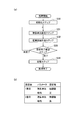
極性判定オフセット計測処理部210での処理フローと積算単位および極性の設定表を図3に示す。極性判定オフセット計測処理が開始されると極性判定ステップS1において、SW1、SW2、SW4を切断状態、SW3を接続状態とし、クロス・バースイッチ33のs11とs13およびs12とs14を接続した状態とs11とs14およびs12とs13を接続した状態とで比較器34から出力される比較信号を取得し、クロス・バースイッチ33の接続状態を低電位電圧が出力される状態にする。以降、クロス・バースイッチ33の接続状態は変化させない。説明上Vofc<0としているため、極性判定ステップS1完了後クロス・バースイッチ33はs11とs13およびs12とs14が接続される。
FIG. 3 shows the processing flow in the polarity determination offset measurement processing unit 210, the integration unit, and the polarity setting table. When the polarity determination offset measurement process is started, in the polarity determination step S1, SW1, SW2, and SW4 are disconnected, SW3 is connected, and s11 and s13 and s12 and s14 of the crossbar switch 33 are connected and s11. The comparison signal output from the comparator 34 is acquired in the state where s14 and s12 and s13 are connected, and the connected state of the crossbar switch 33 is set to the state where the low potential voltage is output. After that, the connection state of the crossbar switch 33 is not changed. Since Vofc <0 for the sake of explanation, s11 and s13 and s12 and s14 are connected to the crossbar switch 33 after the completion of the polarity determination step S1.
この後、SW3を切断状態にして、基準電圧を超える積算回数を計測する。極性判定オフセット計測処理においては、図3(b)の積算単位および極性の設定表に記載したように、はじめに積算単位が粗調整で極性が正の粗調整正積算単位で基準電圧を超える積算回数を計測し、次に積算単位が微調整で極性が負の微調整負積算単位で基準電圧を超える積算回数を計測する。
After this, switch SW3 to the disconnected state and measure the number of integrations exceeding the reference voltage. In the polarity determination offset measurement process, as described in the integration unit and polarity setting table of FIG. 3B, first, the integration unit is coarse adjustment and the polarity is positive. The number of integrations exceeds the reference voltage in the positive integration unit. Then, the integration unit is fine adjustment and the polarity is negative. The number of integrations exceeding the reference voltage is measured in the negative integration unit.
極性判定ステップS1直後の積算単位設定ステップS2では、積算単位および極性の設定表の1番目の積算単位と極性を読んでSW1のみを開閉するように積算部35を制御する。次に積算回数計測処理に遷移し積算単位および極性の設定表の1番目の極性に基づき積算電圧<基準電圧+オフセット電圧となるまで積算を繰返す。図4に積算回数計測ステップS3の処理フローを示す。積算単位の極性が正の時では、積算電圧>基準電圧+オフセット電圧となるまで積算を繰返し、積算単位の極性が負の時では積算電圧<基準電圧+オフセット電圧となるまで積算ステップS10と比較ステップS11を繰返す。積算電圧と基準電圧+オフセット電圧の大小関係の判定は比較器34から出力される比較信号で判定する。比較器34のオフセット電圧Vofc<0の場合、比較器34には基準電圧Vrefおよび比較器34のオフセット電圧の和(Vofc<0のため式上ではVref-Vofc)と積算電圧が入力され、基準電圧とオフセット電圧の和>積算電圧の場合には比較器34から低電位電圧の比較信号が出力される。基準電圧とオフセット電圧の和<積算電圧となると比較信号が高電位電圧となるため図4の比較ステップの処理が可能となる。
In the integration unit setting step S2 immediately after the polarity determination step S1, the integration unit 35 is controlled so as to read the first integration unit and polarity in the integration unit and polarity setting table and open / close only SW1. Next, the process shifts to the integration count measurement process, and the integration is repeated until the integrated voltage <reference voltage + offset voltage is obtained based on the first polarity in the integration unit and polarity setting table. FIG. 4 shows the processing flow of the integration number measurement step S3. When the polarity of the integration unit is positive, the integration is repeated until the integration voltage> reference voltage + offset voltage, and when the polarity of the integration unit is negative, the integration is compared with the integration step S10 until the integration voltage <reference voltage + offset voltage. Step S11 is repeated. The magnitude relationship between the integrated voltage and the reference voltage + offset voltage is determined by the comparison signal output from the comparator 34. When the offset voltage Vofc <0 of the comparator 34, the sum of the reference voltage Vref and the offset voltage of the comparator 34 (Vref-Vofc in the equation because Vofc <0) and the integrated voltage are input to the comparator 34, and the reference voltage is input. When the sum of the voltage and the offset voltage> the integrated voltage, the comparator 34 outputs a low potential voltage comparison signal. When the sum of the reference voltage and the offset voltage is equal to the integrated voltage, the comparison signal becomes a high potential voltage, so that the comparison step of FIG. 4 can be processed.
積算回数計測ステップS3の後、設定完了確認ステップS4において積算単位および極性の設定表に次の設定の有無を確認し、次の設定がある場合では未完了として積算単位設定ステップS2に遷移する。図3(b)の場合では微調整負積算単位となるように積算部35を設定する。微調整負積算単位での積算回数計測ステップS3が完了した後、設定完了確認ステップS4において積算単位および極性の設定表に次の設定が無いことを確認し記憶ステップS5に遷移する。
After the integration number measurement step S3, in the setting completion confirmation step S4, the presence or absence of the following settings is confirmed in the integration unit and polarity setting table, and if there is the next setting, the integration unit setting step S2 is performed as incomplete. In the case of FIG. 3B, the integration unit 35 is set so as to be a fine adjustment negative integration unit. After the integration number measurement step S3 in the fine adjustment negative integration unit is completed, it is confirmed in the setting completion confirmation step S4 that there is no next setting in the integration unit and polarity setting table, and the process proceeds to the storage step S5.
極性判定オフセット計測処理ではじめて積算回数計測ステップS3に遷移した時から記憶ステップS5に遷移までの積算電圧と積算回数の関係の例を図5に示す。ko2+1回目の積算ステップS30後の比較ステップS31で基準電圧とオフセット電圧の和>積算電圧となったとすると、ko2を粗調整オフセット積算回数と定義する。また、微調整負積算単位に設定してから積算ステップを開始してからko+1回目で基準電圧とオフセット電圧の和<積算電圧とすると、koを微調整オフセット積算回数と定義する。記憶ステップS5ではko2およびkoを記憶する。
FIG. 5 shows an example of the relationship between the integrated voltage and the integrated number from the transition from the transition to the integrated number measurement step S3 to the transition to the storage step S5 for the first time in the polarity determination offset measurement process. If the sum of the reference voltage and the offset voltage> the integrated voltage in the comparison step S31 after the ko2 + 1th integration step S30, ko2 is defined as the number of coarse adjustment offset integrations. Further, if the sum of the reference voltage and the offset voltage is equal to the ko + 1th time after the integration step is started after setting the fine adjustment negative integration unit, ko is defined as the number of fine adjustment offset integrations. In the storage step S5, ko2 and ko are stored.
式(1)と式(2)より基準電圧およびオフセット電圧の和と積算電圧には以下の方程式が成立する。
From equations (1) and (2), the following equation holds for the sum of the reference voltage and offset voltage and the integrated voltage.

式(4)のVGp2は粗調整正積算単位を表し、式(5)のVGn1は微調整負積算単位を表す。式(3)の右辺のVGn1δkoは基準電圧およびオフセット電圧の和と記憶ステップS5直前の積算電圧の差を表し、δkoは0以上1未満の実数である。
VGp2 in equation (4) represents a coarse adjustment positive integration unit, and VGn1 in equation (5) represents a fine adjustment negative integration unit. VGn1δko on the right side of the equation (3) represents the difference between the sum of the reference voltage and the offset voltage and the integrated voltage immediately before the storage step S5, and δko is a real number of 0 or more and less than 1.
積算単位相関計測処理部211での処理フローと積算単位および極性の設定表を図6に示す。積算単位相関処理が開始されると、プリチャージ処理においてSW1、SW2、SW4を切断状態、SW3を接続状態としてコンデンサCoにVrefに相当する電荷をプリチャージする(プリチャージステップS20)。この後、SW3を切断状態にして、過剰粗調整積算ステップS21に遷移し、極性判定オフセット計測処理で得られたko2に例えば2を加算した積算回数で粗調整正積算単位を積算する。ko2に加算する数は、1以上の整数であれば幾つであっても良い。
FIG. 6 shows the processing flow in the integration unit correlation measurement processing unit 211 and the setting table of the integration unit and polarity. When the integration unit correlation process is started, in the precharge process, SW1, SW2, and SW4 are disconnected and SW3 is connected, and the capacitor Co is precharged with a charge corresponding to Vref (precharge step S20). After that, the SW3 is disconnected, the process proceeds to the excess coarse adjustment integration step S21, and the coarse adjustment positive integration unit is integrated by the number of integrations obtained by adding, for example, 2 to ko2 obtained by the polarity determination offset measurement process. The number to be added to ko2 may be any number as long as it is an integer of 1 or more.
以降の処理は、極性判定オフセット計測処理の積算単位設定ステップS2以降と同じである。積算単位相関処理ではじめて積算ステップを開始してからkc+1回目で基準電圧とオフセット電圧の和<積算電圧とすると、kcを微調整相関積算回数と定義する。記憶ステップS24ではkcを記憶する。
The subsequent processing is the same as the integration unit setting step S2 and subsequent processing of the polarity determination offset measurement processing. If the sum of the reference voltage and the offset voltage is equal to the sum of the reference voltage and the offset voltage at the kc + 1st time after the integration step is started for the first time in the integration unit correlation processing, kc is defined as the number of fine-tuning correlation integrations. In the storage step S24, kc is stored.
積算単位相関処理では以下の方程式が成立する。
The following equation holds in the integration unit correlation process.
式(6)の右辺のVGn1δkcは基準電圧およびオフセット電圧の和と記憶ステップS24直前の積算電圧の差を表し、δkcは0以上1未満の実数である。
VGn1δkc on the right side of the equation (6) represents the difference between the sum of the reference voltage and the offset voltage and the integrated voltage immediately before the storage step S24, and δkc is a real number of 0 or more and less than 1.
積算単位計測処理部212での処理フローを図7に示す。積算単位計測処理が開始されると、初期化ステップS30において、SW1からSW3を切断状態、SW4を接続状態にした後切断状態にしてコンデンサCoに蓄積された電荷をリセットする。このあとの処理は、極性判定オフセット計測処理ではじめて積算ステップに遷移した以降の処理と同じである。ki2+1回目の積算ステップ後の比較ステップで基準電圧とオフセット電圧の和>積算電圧となったとすると、ki2を粗調整積算回数と定義する。また、積算単位計測処理で微調整負積算単位に設定してからki+1回目で基準電圧とオフセット電圧の和<積算電圧とすると、kiを微調整積算回数と定義する。記憶ステップS34ではki2とkiを記憶する。
FIG. 7 shows the processing flow in the integration unit measurement processing unit 212. When the integration unit measurement process is started, in the initialization step S30, SW1 to SW3 are disconnected, SW4 is connected and then disconnected, and the electric charge accumulated in the capacitor Co is reset. The subsequent processing is the same as the processing after the transition to the integration step for the first time in the polarity determination offset measurement processing. If the sum of the reference voltage and the offset voltage> the integrated voltage in the comparison step after the ki2 + 1th integration step, ki2 is defined as the number of coarse adjustment integrations. Further, if the sum of the reference voltage and the offset voltage is equal to the sum of the reference voltage and the offset voltage at the first ki + 1 after setting the fine adjustment negative integration unit in the integration unit measurement process, ki is defined as the number of fine adjustment integrations. In the storage step S34, ki2 and ki are stored.
積算単位計測処理では以下の方程式が成立する。
The following equation holds in the integration unit measurement process.
式(7)の右辺のVGn1δkiは基準電圧およびオフセット電圧の和と記憶ステップS34直前の積算電圧の差を表し、δkiは0以上1未満の実数である。
VGn1δki on the right side of the equation (7) represents the difference between the sum of the reference voltage and the offset voltage and the integrated voltage immediately before the storage step S34, and δki is a real number of 0 or more and less than 1.
以降の式展開では表記を簡単にするためKo=ko+δko、Kc=kc+δkc、Ki=ki+δkiとする。
In the following formula expansion, Ko = ko + δko, Kc = kc + δkc, Ki = ki + δki to simplify the notation.
式(6)と式(3)の差をとることによりVGn1とVGp2の関係式が以下のように導出できる。
By taking the difference between equations (6) and (3), the relational expression between VGn1 and VGp2 can be derived as follows.

式(8)を式(3)に代入するとVofcとVGn1の関係式が導出できる。
By substituting equation (8) into equation (3), the relational expression between Vofc and VGn1 can be derived.

式(8)と式(9)を式(6)に代入することによりVGn1の式を得る。
The equation of VGn1 is obtained by substituting the equations (8) and (9) into the equation (6).

式(10)を式(8)、式(9)に代入することで、それぞれVGp2とVofcの表式を得る。
By substituting the equation (10) into the equations (8) and (9), the expressions of VGp2 and Vofc are obtained, respectively.

通常、Vref>|Vofc|であるため、ki2>ko2となる。VGn1、VGp2、Vofcに含まれるδki、δkc、δkoは0以上1未満の実数であるが、具体的な値は不明である。このδki、δkc、δkoの不確かさのためVGn1、VGp2、Vofcのとり得る値は範囲を持つ。VGn1、VGp2、Vofcの校正値は、VGn1、VGp2、Vofcの範囲の中央値により決定する。式(10)をδki、δkc、δkoで偏微分すると以下の式を得る。
Normally, it is Vref> | Vofc |, so ki2> ko2. Δki, δkc, and δko contained in VGn1, VGp2, and Vofc are real numbers of 0 or more and less than 1, but their specific values are unknown. Due to the uncertainty of δki, δkc, and δko, the possible values of VGn1, VGp2, and Vofc have a range. The calibration value of VGn1, VGp2, and Vofc is determined by the median value in the range of VGn1, VGp2, and Vofc. The following equation is obtained by partially differentiating equation (10) with respect to δki, δkc, and δko.

式(13)から式(15)よりVGn1はδkcに対しては単調増加でありδkiとδkoに対しては単調減少である。したがって、VGn1の範囲は以下の式で表される。
From equations (13) to (15), VGn1 increases monotonically with respect to δkc and decreases monotonically with respect to δki and δko. Therefore, the range of VGn1 is expressed by the following equation.
式(16)から中央値を導出することによりVGn1の校正値VGn1cが以下の式のように得られる。
By deriving the median value from equation (16), the calibration value VGn1c of VGn1 can be obtained as shown in the following equation.
式(11)をδki、δkc、δkoで偏微分すると以下の式を得る。
The following equation is obtained by partially differentiating equation (11) with respect to δki, δkc, and δko.

式(18)と式(19)より、VGp2はδkiに対しては単調増加であり、δkoに対しては単調減少である。式(20)においてKi>Koの場合は∂VGp2/∂(δkc)<0となり、Ki<Koの場合は∂VGp2/∂(δkc)>0となる。したがって、Ki>Koの場合ではVGp2はδkcに対して単調減少であり、Ki<Koの場合ではVGp2はδkcに対して単調増加となる。これらの関係よりKi>Koの場合ではVGp2の範囲は次の式で与えられ、その中央値をとることによりKi>Koの場合の校正値VGp2cは式(22)となる。
From equations (18) and (19), VGp2 is monotonically increasing with respect to δki and decreasing monotonically with respect to δko. In equation (20), if Ki> Ko, then ∂VGp2 / ∂ (δkc) <0, and if Ki <Ko, then ∂VGp2 / ∂ (δkc)> 0. Therefore, in the case of Ki> Ko, VGp2 is monotonically decreasing with respect to δkc, and in the case of Ki <Ko, VGp2 is monotonically increasing with respect to δkc. From these relationships, the range of VGp2 in the case of Ki> Ko is given by the following equation, and by taking the median value, the calibration value VGp2c in the case of Ki> Ko becomes equation (22).

また、Ki<Koの場合ではVGp2の範囲は式(23)で与えられ、その中央値をとることによりKi>Koの場合の校正値VGp2cは式(24)となる。
Also, in the case of Ki <Ko, the range of VGp2 is given by equation (23), and by taking the median value, the calibration value VGp2c in the case of Ki> Ko becomes equation (24).

式(12)をδki、δkc、δkoで偏微分すると以下の式を得る。
The following equation is obtained by partially differentiating equation (12) with respect to δki, δkc, and δko.

式(25)と式(26)よりVofcはδkiに対しては単調減少であり、δkoに対しては単調増加である。式(27)において(ko2+1)Ki > (ki2+1)Koの場合では∂Vofc/∂(δkc)>0となり、(ko2+1)Ki < (ki2+1)Koの場合では∂Vofc/∂(δkc)<0となる。これらの関係より(ko2+1)Ki > (ki2+1)Koの場合ではVofcの範囲は式(28)で与えられ、その中央値をとることにより(ko2+1)Ki > (ki2+1)Koの場合の校正値Vofccは式(29)となる。
From equations (25) and (26), Vofc is a monotonous decrease for δki and a monotonous increase for δko. In equation (27), ∂Vofc / ∂ (δkc)> 0 in the case of (ko2 + 1) Ki> (ki2 + 1) Ko, and ∂Vofc in the case of (ko2 + 1) Ki <(ki2 + 1) Ko. / ∂ (δkc) <0. From these relationships, in the case of (ko2 + 1) Ki> (ki2 + 1) Ko, the range of Vofc is given by equation (28), and by taking the median value, (ko2 + 1) Ki> (ki2 + 1) ) The calibration value Vofcc in the case of Ko is given by Eq. (29).

また、(ko2+1)Ki < (ki2+1)Koの場合ではVofcの範囲は式(30)で与えられ、その中央値をとることにより(ko2+1)Ki < (ki2+1)Koの場合の校正値Vofccは式(31)となる。
In the case of (ko2 + 1) Ki <(ki2 + 1) Ko, the range of Vofc is given by Eq. (30), and by taking the median value, (ko2 + 1) Ki <(ki2 + 1) Ko The calibration value Vofcc in the case of is given by Eq. (31).

以上の説明で示したように校正状態における極性判定オフセット計測処理、積算単位相関処理、積算単位計測処理により、積算単位VGn1、VGp2と比較器のオフセット電圧Vofcの校正値であるVGn1c、VGp2c、Vofccを得ることができる。
As shown in the above explanation, by the polarity determination offset measurement processing, integration unit correlation processing, and integration unit measurement processing in the calibration state, the integration units VGn1, VGp2 and the calibrated values of the offset voltage Vofc of the comparator VGn1c, VGp2c, Vofcc Can be obtained.
上述ではVofc<0の場合で説明したが、Vofc>0の場合ではクロス・バースイッチ33のs11とs14およびs12とs13を接続した状態で比較器34から低電位電圧が出力される。このため、クロス・バースイッチ33のs 11とs14およびs12とs13を接続した状態で以降の極性判定オフセット計測処理、積算単位相関処理、積算単位計測処理を実施する。Vofc>0の場合の極性判定オフセット計測処理、積算単位相関処理、積算単位計測処理の処理フローはそれぞれ図3、図6、図7に示した処理フローと同じである。
In the above, the case of Vofc <0 was explained, but in the case of Vofc> 0, the low potential voltage is output from the comparator 34 with the crossbar switches 33 s11 and s14 and s12 and s13 connected. Therefore, the subsequent polarity determination offset measurement processing, integration unit correlation processing, and integration unit measurement processing are performed with the crossbar switches 33 s11 and s14 and s12 and s13 connected. The processing flows of the polarity determination offset measurement processing, the integration unit correlation processing, and the integration unit measurement processing when Vofc> 0 are the same as the processing flows shown in FIGS. 3, 6, and 7, respectively.
クロス・バースイッチ33のs11とs14およびs12とs13を接続した状態で正電流源とコンデンサCoを接続した場合の等価回路モデルを図8(a)に示す。正電流源350で積算する時ではSW2からSW4を切断状態にしてSW1を所定の時間Δtのあいだ接続状態にした後SW1を切断状態にすることを繰返す。これをkp回繰返した時の正電流源から供給される電荷はIp kp Δt となる。比較器34の負の入力側に存在する寄生容量Cp2を考慮すると、積算電圧は以下の式で表される。
FIG. 8 (a) shows an equivalent circuit model when the positive current source and the capacitor Co are connected with the cross bar switches 33 s11 and s14 and s12 and s13 connected. When integrating with the positive current source 350, SW2 to SW4 are disconnected, SW1 is connected for a predetermined time Δt, and then SW1 is disconnected repeatedly. When this is repeated kp times, the charge supplied from the positive current source is Ip kp Δt. Considering the parasitic capacitance Cp2 existing on the negative input side of the comparator 34, the integrated voltage is expressed by the following equation.
負電流で積算する場合では、SW1、SW3、SW4を切断状態にして所定の時間ΔtのあいだSW2を接続状態にした後切断状態にすることを繰返す。クロス・バースイッチ33のs11とs13およびs12とs14を接続し負電流源351とコンデンサCoを接続した時の等価回路を図8(b)に示す。SW2を接続状態にすることをkn回繰返した時では、負電流源351とコンデンサCoを接続する前の電荷(Co+Cp2)Vo,0から負電流源351によってIn knΔt (In>0)の電荷が除去されるため、積算電圧は以下の式で表される。
When integrating with a negative current, SW1, SW3, and SW4 are disconnected, SW2 is connected for a predetermined time Δt, and then disconnected. FIG. 8B shows an equivalent circuit when s11 and s13 and s12 and s14 of the crossbar switch 33 are connected and a negative current source 351 and a capacitor Co are connected. When the connection state of SW2 is repeated kn times, the charge (Co + Cp2) Vo, 0 before connecting the negative current source 351 and the capacitor Co is changed to In knΔt (In> 0) by the negative current source 351. Since the charge is removed, the integrated voltage is expressed by the following equation.
式(1)と式(2)で表されるVofc<0の場合と比較すると、Vofc>0の場合は比較器34の入力をクロス・バースイッチ33で切り替えたために寄生容量が異なるのみで他はVofc<0の場合と同じとなる。このため、Vofc>0の場合の粗調整正積算単位VGp2と微調整負積算単位VGn1は以下の式となる。
Compared with the case of Vofc <0 represented by the equations (1) and (2), in the case of Vofc> 0, the input of the comparator 34 is switched by the crossbar switch 33, so that the parasitic capacitance is different. Is the same as for Vofc <0. Therefore, when Vofc> 0, the coarse adjustment positive integration unit VGp2 and the fine adjustment negative integration unit VGn1 are given by the following equations.

図3に示した極性判定オフセット計測処理部210の処理フローにより粗調整オフセット積算回数ko2と微調整オフセット積算回数koを得る。図7の等価回路から比較器の正の入力は等価的にVref+Vofcとなり負の入力は積算電圧となるため、ko2およびkoとVref、Vofc、VGn1、VGp2には以下の関係式が成立する。
The coarse adjustment offset integration number ko2 and the fine adjustment offset integration number ko are obtained from the processing flow of the polarity determination offset measurement processing unit 210 shown in FIG. From the equivalent circuit of FIG. 7, the positive input of the comparator is equivalently Vref + Vofc and the negative input is the integrated voltage. Therefore, the following relational expression holds for ko2 and ko and Vref, Vofc, VGn1, and VGp2. ..
式(36)の右辺のVGn1δkoは基準電圧およびオフセット電圧の和と記憶ステップ直前の積算電圧の差を表し、δkoは0以上1未満の実数である。
VGn1δko on the right side of equation (36) represents the difference between the sum of the reference voltage and offset voltage and the integrated voltage immediately before the storage step, and δko is a real number greater than or equal to 0 and less than 1.
図6に示した積算単位相関計測処理部211での処理フローにより微調整相関積算回数kcを得る。ko2およびkcと、Vref、Vofc、VGn1、VGp2には以下の関係式が成立する。
The fine-tuned correlation integration number kc is obtained from the processing flow in the integration unit correlation measurement processing unit 211 shown in FIG. The following relational expressions hold for ko2 and kc, and for Vref, Vofc, VGn1, and VGp2.
式(37)の右辺のVGn1δkcは基準電圧およびオフセット電圧の和と記憶ステップS34直前の積算電圧の差を表し、δkcは0以上1未満の実数である。
VGn1δkc on the right side of the equation (37) represents the difference between the sum of the reference voltage and the offset voltage and the integrated voltage immediately before the storage step S34, and δkc is a real number of 0 or more and less than 1.
図7に示した積算単位計測処理部での処理フローにより粗調整積算回数ki2と微調整積算回数kiを得る。ki2およびkiと、Vref、Vofc、VGn1、VGp2には以下の関係式が成立する。
The rough adjustment integration number ki2 and the fine adjustment integration number ki are obtained from the processing flow in the integration unit measurement processing unit shown in FIG. The following relational expressions hold for ki2 and ki, Vref, Vofc, VGn1, and VGp2.
式(38)の右辺のVGn1δkiは基準電圧およびオフセット電圧の和と記憶ステップS34直前の積算電圧の差を表し、δkiは0以上1未満の実数である。
VGn1δki on the right side of the equation (38) represents the difference between the sum of the reference voltage and the offset voltage and the integrated voltage immediately before the storage step S34, and δki is a real number of 0 or more and less than 1.
以降の式展開では表記を簡単にするためKo=ko+δko、Kc=kc+δkc、Ki=ki+δkiとする。
In the following formula expansion, Ko = ko + δko, Kc = kc + δkc, Ki = ki + δki to simplify the notation.
式(37)と式(36)の差をとることによりVGn1とVGp2の関係式が導出でき、VGn1とVGp2の関係式はVofc>0の場合も式(8)となる。式(8)を式(36)に代入するとVofcとVGn1の関係式が導出できる。
By taking the difference between equations (37) and (36), the relational expression between VGn1 and VGp2 can be derived, and the relational expression between VGn1 and VGp2 becomes equation (8) even when Vofc> 0. By substituting Eq. (8) into Eq. (36), the relational expression between Vofc and VGn1 can be derived.

式(8)と式(39)を式(38)に代入することによりVofc>0の場合のVGn1を導出できる。結果的にVofc>0の場合のVGn1は式(10)となる。このためVofc>0の場合のVGp2は式(11)となる。式(10)を式(39)に代入することでVofcが得られ以下の式で表される。
By substituting equations (8) and (39) into equation (38), VGn1 when Vofc> 0 can be derived. As a result, VGn1 when Vofc> 0 is given by Eq. (10). Therefore, VGp2 when Vofc> 0 is given by Eq. (11). By substituting Eq. (10) into Eq. (39), Vofc is obtained and expressed by the following equation.
Vofc<0の場合と比較するとVGn1とVGp2は同じであり、Vofcは符号が異なるのみで絶対値は同じである。
Compared with the case of Vofc <0, VGn1 and VGp2 are the same, and Vofc has the same absolute value except for the sign.
Vofc>0の場合もVofc<0の場合と同様にVGn1、VGp2、Vofcの校正値は、VGn1、VGp2、Vofcの範囲の中央値により決定する。Vofc>0の場合のVGn1はVofc<0の場合と同じであるためVGn1の範囲は式(16)で表され、校正値VGn1cは式(17)となる。VGp2も同様にVofc>0の場合の校正値VGp2cはKi<Koの場合では式(23)となり、Ki>Koの場合では式(24)となる。
When Vofc> 0, the calibration values of VGn1, VGp2, and Vofc are determined by the median of the range of VGn1, VGp2, and Vofc, as in the case of Vofc <0. Since VGn1 when Vofc> 0 is the same as when Vofc <0, the range of VGn1 is expressed by Eq. (16), and the calibration value VGn1c is Eq. (17). Similarly, for VGp2, the calibration value VGp2c when Vofc> 0 is Eq. (23) when Ki <Ko, and Eq. (24) when Ki> Ko.
Vofc>0の場合のVofcはVofc<0の場合と符号が異なるだけであるため、式(40)をδki、δkc、δkoで偏微分すると以下の式を得る。
Since Vofc in the case of Vofc> 0 only has a different sign from the case of Vofc <0, the following equation is obtained by partially differentiating equation (40) with respect to δki, δkc, and δko.

式(41)と式(42)よりVofcはδkiに対しては単調増加であり、δkoに対しては単調減少である。式(43)において(ko2+1)Ki > (ki2+1)Koの場合では∂Vofc/∂(δkc)<0となり、(ko2+1)Ki < (ki2+1)Koの場合では∂Vofc/∂(δkc)>0となる。これらの関係より(ko2+1)Ki > (ki2+1)Koの場合ではVofcの範囲は式(44)で与えられ、その中央値をとることにより(ko2+1)Ki > (ki2+1)Koの場合の校正値Vofccは式(45)となる。
From equations (41) and (42), Vofc is a monotonous increase for δki and a monotonous decrease for δko. In equation (43), ∂Vofc / ∂ (δkc) <0 in the case of (ko2 + 1) Ki> (ki2 + 1) Ko, and ∂Vofc in the case of (ko2 + 1) Ki <(ki2 + 1) Ko. / ∂ (δkc)> 0. From these relationships, in the case of (ko2 + 1) Ki> (ki2 + 1) Ko, the range of Vofc is given by equation (44), and by taking the median value, (ko2 + 1) Ki> (ki2 + 1) ) The calibration value Vofcc in the case of Ko is given by Eq. (45).

また、(ko2+1)Ki < (ki2+1)Koの場合ではVofcの範囲は式(46)で与えられ、その中央値をとることにより(ko2+1)Ki < (ki2+1)Koの場合の校正値Vofccは式(47)となる。
In the case of (ko2 + 1) Ki <(ki2 + 1) Ko, the range of Vofc is given by Eq. (46), and by taking the median value, (ko2 + 1) Ki <(ki2 + 1) Ko The calibration value Vofcc in the case of is given by Eq. (47).

以上の説明で示したようにVofc>0の場合でも校正状態における極性判定オフセット計測処理、積算単位相関処理、積算単位計測処理により、積算単位VGn1、VGp2と比較器のオフセット電圧Vofcの校正値であるVGn1c、VGp2c、Vofccを得ることができる。
As shown in the above explanation, even when Vofc> 0, the calibration values of the integration units VGn1 and VGp2 and the offset voltage Vofc of the comparator are used by the polarity judgment offset measurement processing, integration unit correlation processing, and integration unit measurement processing in the calibration state. You can get some VGn1c, VGp2c, Vofcc.
変換状態の処理は変換制御部22で制御される。変換制御部22の処理フローと積算単位および極性の設定表を図9に示す。変換状態においては、校正状態の極性判定オフセット計測処理で得られたVofcの極性に基づいたクロス・バースイッチ33の接続を維持する。初期化ステップS40において切替部32のa10とc10を接続してサンプルホールド部31で入力電圧をホールドするとともに、SW1~SW3を切断してSW4の接続・切断によりコンデンサCoの蓄積された電荷をリセットする。
The processing of the conversion state is controlled by the conversion control unit 22. FIG. 9 shows the processing flow of the conversion control unit 22 and the setting table of the integration unit and the polarity. In the conversion state, the connection of the crossbar switch 33 based on the polarity of Vofc obtained by the polarity determination offset measurement process in the calibration state is maintained. In the initialization step S40, a10 and c10 of the switching unit 32 are connected to hold the input voltage at the sample hold unit 31, and SW1 to SW3 are disconnected to reset the accumulated charge of the capacitor Co by connecting / disconnecting SW4. To do.
以降の処理は積算単位計測処理の基準電圧が入力電圧となること以外は積算単位計測処理と同じである。この処理により粗調整変換積算回数kv2と微調整変換積算回数kvを得る。入力電圧をVinとするとkv2およびkvと以下の関係式が成立する。
The subsequent processing is the same as the integration unit measurement process except that the reference voltage of the integration unit measurement process becomes the input voltage. By this process, the coarse adjustment conversion integration number kv2 and the fine adjustment conversion integration number kv are obtained. When the input voltage is Vin, the following relational expression holds between kv2 and kv.
Vofc<0とVofc>0の場合とではVofccは異なるが、Vofcの極性とクロス・バースイッチの接続を考慮すると、Vofc<0とVofc>0の両方の場合で|Vofcc|となるため式(48)の左辺をVin+|Vofcc|とした。式(48)の右辺のVGn1cδkvは入力電圧およびオフセット電圧の和と記憶ステップ直前の積算電圧の差を表し、δkvは0以上1未満の実数であるが具体的な値は不明である。このδkvの不確かさのためVinのとり得る値は範囲を持つ。Vinの変換値はVinの範囲の中央値により決定する。Vinの範囲は式(49)となりVinの変換値Vincは式(50)で表される。
Vofcc is different for Vofc <0 and Vofc> 0, but considering the polarity of Vofc and the connection of the crossbar switch, it becomes | Vofcc | in both cases of Vofc <0 and Vofc> 0. The left side of 48) is Vin + | Vofcc |. VGn1cδkv on the right side of the equation (48) represents the difference between the sum of the input voltage and the offset voltage and the integrated voltage immediately before the storage step, and δkv is a real number of 0 or more and less than 1, but the specific value is unknown. Due to this uncertainty of δkv, the possible values of Vin have a range. The conversion value of Vin is determined by the median value of the Vin range. The range of Vin is given by the equation (49), and the converted value Vinc of Vin is expressed by the equation (50).

以上の変換制御部22の処理により、校正状態で得た校正値VGn1c、VGp2c、Vofccを用いて入力電圧の変換値Vincを得ることができる。
By the above processing of the conversion control unit 22, the conversion value Vinc of the input voltage can be obtained by using the calibration values VGn1c, VGp2c, and Vofcc obtained in the calibration state.
以上の説明で示した実施形態により、比較器34のオフセットや積算単位を構成する容量等が経時変化により変動しても、比較器34のオフセットとDAコンバータのアナログ値出力部である積算部35の校正が可能であり長期安定性の高いADコンバータを提供できる。
According to the embodiment shown in the above description, even if the offset of the comparator 34 and the capacity constituting the integration unit fluctuate due to aging, the offset of the comparator 34 and the integration unit 35 which is the analog value output unit of the DA converter It is possible to provide an AD converter that can be calibrated and has high long-term stability.
校正値の精度を高くするためには積算単位を小さくすればよいが、1種類の積算単位のみを使用した場合では高精度化のために積算単位を小さくすると校正状態での各処理における積算回数が多くなり処理に要する時間が長くなる。本実施形態のように粗調整と微調整の2種の積算単位を設けることにより、小さな積算単位のみで積算する場合と比較して少ない積算回数でかつ高精度に積算電圧を基準電圧または入力電圧にまで積算することができる。これにより、校正処理と変換処理が小さな積算単位のみで積算する場合と比較して少ない積算回数でかつ高精度に実施できる。
In order to improve the accuracy of the calibration value, it is sufficient to reduce the integration unit, but when only one type of integration unit is used, if the integration unit is reduced to improve the accuracy, the number of integrations in each process in the calibration state Will increase and the time required for processing will increase. By providing two types of integration units, coarse adjustment and fine adjustment, as in the present embodiment, the integrated voltage can be integrated with a reference voltage or input voltage with a small number of integrations and with high accuracy as compared with the case of integrating with only a small integration unit. Can be accumulated up to. As a result, the calibration process and the conversion process can be performed with a small number of integrations and with high accuracy as compared with the case where the integration processing is performed only in a small integration unit.
図10に第1実施形態の変形例を示す。図10に示す自己校正機能付きADコンバータ200は、上記の第1実施形態から、可変正電流源550と可変負電流源551を使用した積算部55と、校正制御部41に多重積算単位計測処理部410が追加された点で異なる。また、変換制御部42の処理フローが異なる。
FIG. 10 shows a modified example of the first embodiment. In the AD converter 200 with a self-calibration function shown in FIG. 10, from the first embodiment described above, the integration unit 55 using the variable positive current source 550 and the variable negative current source 551 and the calibration control unit 41 are subjected to multiple integration unit measurement processing. It differs in that part 410 is added. Further, the processing flow of the conversion control unit 42 is different.
可変正電流源550では積算電圧を増加させる粗調整正積算単位、微調整正積算単位の2種の積算単位を生成し、制御部からの信号MAGPにより粗調整正積算単位と微調整正積算単位を生成する電流が設定される。可変負電流源551では積算電圧を減少させる粗調整負積算単位、微調整負積算単位の2種の積算単位を生成し、制御部40からの信号MAGNにより粗調整負積算単位と微調整負積算単位を生成する電流が設定される。
The variable positive current source 550 generates two types of integration units, a coarse adjustment positive integration unit and a fine adjustment positive integration unit that increase the integrated voltage, and a coarse adjustment positive integration unit and a fine adjustment positive integration unit are generated by the signal MAGP from the control unit. The current that produces is set. The variable negative current source 551 generates two types of integration units, a coarse adjustment negative integration unit and a fine adjustment negative integration unit that reduce the integrated voltage, and a coarse adjustment negative integration unit and a fine adjustment negative integration unit are generated by the signal MAGN from the control unit 40. The current that produces the unit is set.
以下の説明において粗調整正積算単位をVGp2、微調整正積算単位をVGp1、粗調整負積算単位をVGn2、微調整負積算単位をVGn1とする。
In the following explanation, the coarse adjustment positive integration unit is VGp2, the fine adjustment positive integration unit is VGp1, the coarse adjustment negative integration unit is VGn2, and the fine adjustment negative integration unit is VGn1.
校正状態においては、校正制御部41の極性判定オフセット計測処理部210、積算単位相関計測処理部211、多重積算単位計測処理部410、積算単位計測処理部212により、それぞれ極性判定オフセット計測処理、積算単位相関処理、多重積算単位計測処理、積算単位計測処理を実施する。
In the calibration state, the polarity determination offset measurement processing unit 210, the integration unit correlation measurement processing unit 211, the multiple integration unit measurement processing unit 410, and the integration unit measurement processing unit 212 of the calibration control unit 41 perform polarity determination offset measurement processing and integration, respectively. Carry out unit correlation processing, multiple integration unit measurement processing, and integration unit measurement processing.
可変正電流源550を設定して粗調整正積算単位VGp2を生成させ、可変負電流源551を設定して微調整負積算単位VG1nを生成させた状態で、極性判定オフセット計測処理と積算単位相関計測処理を実施する。これらの処理は図1の場合と同じであるため割愛する。これらの処理によりVofc<0の場合では式(3)と式(6)の関係式が成立し、Vofc>0の場合では式(36)と式(37)の関係式が成立する粗調整オフセット積算回数ko2、微調整オフセット積算回数ko、微調整相関積算回数kcが得られる。
With the variable positive current source 550 set to generate the coarse adjustment positive integration unit VGp2 and the variable negative current source 551 to generate the fine adjustment negative integration unit VG1n, the polarity determination offset measurement process and the integration unit correlation Carry out the measurement process. Since these processes are the same as in FIG. 1, they are omitted. By these processes, when Vofc <0, the relational expression between Eqs. (3) and (6) is established, and when Vofc> 0, the relational expression between Eqs. (36) and (37) is satisfied. The number of integrations ko2, the number of fine adjustment offset integrations ko, and the number of fine adjustment correlation integrations kc can be obtained.
図11に多重積算単位計測処理部410の処理フローを示す。多重積算単位計測処理が開始されると、SW1、SW2、SW4を切断しSW3を接続してコンデンサCoをプリチャージし積算電圧の初期値を基準電圧Vrefとする(ステップS50)。この後SW3を切断して、第1積算ステップS51において、可変正電流源を設定して粗調整負積算単位VGn2を生成させ、S予め決定する所定の回数ke2回SW2を接続・切断して積算電圧からke2 VGn2を除去する。あとは、極性判定オフセット計測処理の積算単位設定ステップ以降と同じ処理を実施する。
FIG. 11 shows the processing flow of the multiple integration unit measurement processing unit 410. When the multiple integration unit measurement process is started, SW1, SW2, and SW4 are disconnected, SW3 is connected, the capacitor Co is precharged, and the initial value of the integrated voltage is set as the reference voltage Vref (step S50). After that, SW3 is disconnected, and in the first integration step S51, a variable positive current source is set to generate a coarse adjustment negative integration unit VGn2, and S is connected and disconnected from SW2 a predetermined number of times predetermined times to integrate. Remove ke2 VGn2 from the voltage. After that, the same processing as after the integration unit setting step of the polarity determination offset measurement processing is performed.
ke2+1回目の積算ステップで基準電圧+オフセット電圧>積算電圧となったとするとke2を第2の粗調整負係数積算回数と定義する。微調整負積算単位に設定してからke+1回目の積算ステップで基準電圧とオフセット電圧の和<積算電圧となったとすると、keを第1の粗調整負係数積算回数と定義する。記憶ステップS55ではkeを記憶する。keに関してはVofc<0の場合では以下の式が成立する。
If the reference voltage + offset voltage> integrated voltage in the ke2 + 1st integration step, ke2 is defined as the second coarse adjustment negative coefficient integration number. Assuming that the sum of the reference voltage and the offset voltage is equal to the integrated voltage in the ke + 1st integration step after setting the fine adjustment negative integration unit, ke is defined as the first coarse adjustment negative coefficient integration number. In the storage step S55, ke is stored. For ke, the following equation holds when Vofc <0.
式(51)において右辺のVGn1δkeは基準電圧およびオフセット電圧の和と記憶ステップ直前の積算電圧の差を表し、δkeは0以上1未満の実数である。
In equation (51), VGn1δke on the right side represents the difference between the sum of the reference voltage and offset voltage and the integrated voltage immediately before the storage step, and δke is a real number of 0 or more and less than 1.
Vofc>0の場合では以下の式(52)が成立する。
When Vofc> 0, the following equation (52) holds.
積算単位計測処理は、可変正電流源550を設定して粗調整正積算単位VGp2を生成させ、可変負電流源551を設定して微調整負積算単位VG1nを生成させた状態で実施する。この処理は図1の場合と同じであるため割愛する。この処理によりVofc<0の場合では式(7)の関係式が成立し、Vofc>0の場合では式(38)の関係式が成立する粗調整積算回数ki2と微調整積算回数kiが得られる。
The integration unit measurement process is performed in a state where the variable positive current source 550 is set to generate the coarse adjustment positive integration unit VGp2, and the variable negative current source 551 is set to generate the fine adjustment negative integration unit VG1n. Since this process is the same as in FIG. 1, it is omitted. By this process, when Vofc <0, the relational expression of Eq. (7) is established, and when Vofc> 0, the rough adjustment integration number ki2 and the fine adjustment integration number ki, for which the relational expression of Eq. (38) is satisfied, are obtained. ..
VGp2、VGn1、Vofcとko2、ko、kc、ki2、ki1の関係式は図1の実施形態の場合と同じであるため、VGp2、VGn1、Vofcの校正値は図1の実施形態で導出したそれぞれの校正値と同じである。
Since the relational expressions between VGp2, VGn1, Vofc and ko2, ko, kc, ki2, and ki1 are the same as in the embodiment of FIG. 1, the calibration values of VGp2, VGn1, and Vofc are derived in the embodiment of FIG. 1, respectively. It is the same as the calibration value of.
VGn2に関しては、Vofc<0の場合では、式(51)と式(3)の差をとり式(8)と式(10)を代入して以下の式(53)が得られる。
Regarding VGn2, in the case of Vofc <0, the following equation (53) is obtained by taking the difference between equations (51) and (3) and substituting equations (8) and (10).

式(53)においてKo=ko+δko、Kc=kc+δkc、Ke=ke+δkeとした。
In equation (53), Ko = ko + δko, Kc = kc + δkc, and Ke = ke + δke.
VGn2に含まれるδkc、δko、δkeは0以上1未満の実数であるが、具体的な値は不明である。このδkc、δko、δkeの不確かさのためVGn2のとり得る値は範囲を持つ。VGn2の校正値はVGn2の範囲の中央値により決定する。また、VGn1には校正値VGn1cを用いる。式(53)をδkc、δko、δkeで偏微分すると以下の式を得る。
Δkc, δko, δke contained in VGn2 are real numbers of 0 or more and less than 1, but the specific values are unknown. Due to the uncertainty of δkc, δko, and δke, the possible values of VGn2 have a range. The calibration value of VGn2 is determined by the median value of the range of VGn2. The calibration value VGn1c is used for VGn1. The following equation is obtained by partially differentiating equation (53) with respect to δkc, δko, and δke.

上式の不等号の導出にはVGn1c<0、kp2>ko2を用いた。式(54)から式(56)によりVGn2はδkeとδkoに対しては単調増加であり、δkcに対しては単調減少である。このためVGn2の範囲は式(57)となり、この中央値をとることにより校正値VGn2cは式(58)で表される。
VGn1c <0, kp2> ko2 was used to derive the inequality sign in the above equation. From equations (54) to (56), VGn2 is monotonically increasing with respect to δke and δko and monotonically decreasing with respect to δkc. Therefore, the range of VGn2 is given by the equation (57), and the calibration value VGn2c is expressed by the equation (58) by taking the median value.

以上の説明で示したように校正状態における極性判定オフセット計測処理、積算単位相関処理、多重積算単位計測処理、積算単位計測処理により、積算単位VGn1、VGp2、VGn2と比較器のオフセット電圧Vofcの校正値であるVGn1c、VGp2c、VGn2c、Vofccを得ることができる。
As shown in the above explanation, the polarity determination offset measurement processing, integration unit correlation processing, multiple integration unit measurement processing, and integration unit measurement processing in the calibration state are used to calibrate the integration units VGn1, VGp2, VGn2 and the offset voltage Vofc of the comparator. The values VGn1c, VGp2c, VGn2c and Vofcc can be obtained.
変換状態で実施する変換制御部の処理フローを図12に示す。変換状態においては、校正状態の極性判定オフセット計測処理で得られたVofcの極性に基づいたクロス・バースイッチ33の接続を維持する。変換制御部42の処理が開始されると基準電圧比較ステップS60において、切替部32のa10とc10を接続してサンプルホールド部31で入力電圧をホールドするとともに、SW1、SW2、SW4を切断してSW3の接続によりコンデンサCoを基準電圧に相当する電荷でプリチャージする。この後、サンプルホールド部31でホールドされた入力電圧と基準電圧を比較器34で比較するとともにSW3を切断する。入力電圧のほうが大きい場合は設定表1読込ステップS61へ遷移し、入力電圧のほうが小さい場合は設定表2読込ステップS62に遷移する。以下では例として、入力電圧が小さい場合で説明する。
FIG. 12 shows the processing flow of the conversion control unit that is executed in the conversion state. In the conversion state, the connection of the crossbar switch 33 based on the polarity of Vofc obtained by the polarity determination offset measurement process in the calibration state is maintained. When the processing of the conversion control unit 42 is started, in the reference voltage comparison step S60, a10 and c10 of the switching unit 32 are connected, the input voltage is held by the sample holding unit 31, and SW1, SW2, and SW4 are disconnected. By connecting SW3, the capacitor Co is precharged with a charge corresponding to the reference voltage. After that, the input voltage held by the sample hold unit 31 and the reference voltage are compared by the comparator 34, and the SW3 is disconnected. If the input voltage is larger, the process proceeds to the setting table 1 reading step S61, and if the input voltage is smaller, the process proceeds to the setting table 2 reading step S62. In the following, as an example, the case where the input voltage is small will be described.
設定表1読込ステップS61に遷移した時は、積算単位および極性の設定表2を読込んだ後、積算単位および極性の設定表2に従って、粗調整負積算単位での積算回数である粗調整負変換積算回数kvn2、粗調整正積算単位での積算回数である粗調整正変換積算回数kv2、微調整負積算単位での積算回数である微調整負変換積算回数kvを得て、記憶ステップS66でkvn2、kv2、kvを記憶する。入力電圧とkvn2、kv2、kvの間には以下の関係式が成立する。
When transitioning to the setting table 1 reading step S61, after reading the integration unit and polarity setting table 2, the coarse adjustment negative is the number of integrations in the integration unit and polarity setting table 2. Obtain the conversion integration number kvn2, the coarse adjustment positive conversion integration number kv2 which is the integration number in the coarse adjustment positive integration unit, and the fine adjustment negative conversion integration number kv which is the integration number in the fine adjustment negative integration unit, and in the storage step S66. Memorize kvn2, kv2, kv. The following relational expression holds between the input voltage and kvn2, kv2, and kv.
Vofc<0とVofc>0の場合とではVofccは異なるが、Vofcの極性とクロス・バースイッチの接続を考慮すると、Vofc<0とVofc>0の両方の場合で|Vofcc|となるため式(59)の左辺をVin+|Vofcc|とした。式(59)の右辺のVGn1cδkvは入力電圧およびオフセット電圧の和と記憶ステップ直前の積算電圧の差を表し、δkvは0以上1未満の実数であるが具体的な値は不明である。このδkvの不確かさのためVinのとり得る値は範囲を持つ。Vinの変換値はVinの範囲の中央値により決定する。Vinの変換値Vincは式(60)で表される。
Vofcc is different for Vofc <0 and Vofc> 0, but considering the polarity of Vofc and the connection of the crossbar switch, the formula is | Vofcc | for both Vofc <0 and Vofc> 0 ( The left side of 59) is Vin + | Vofcc |. VGn1cδkv on the right side of the equation (59) represents the difference between the sum of the input voltage and the offset voltage and the integrated voltage immediately before the storage step, and δkv is a real number of 0 or more and less than 1, but the specific value is unknown. Due to this uncertainty of δkv, the possible values of Vin have a range. The conversion value of Vin is determined by the median value of the Vin range. The conversion value Vinc of Vin is expressed by the equation (60).
基準電圧比較ステップS60において入力電圧が大きい場合では、積算単位および極性の設定表1を読込むため、記憶ステップまでの処理で、kv2、kvが得られる。この場合のVinの変換値は式(50)と同じとなる。
When the input voltage is large in the reference voltage comparison step S60, the integration unit and polarity setting table 1 is read, so that kv2 and kv can be obtained by the processing up to the storage step. The conversion value of Vin in this case is the same as that in the equation (50).
以上の変換制御部42の処理により、校正状態で得た校正値VGn1c、VGp2c、VGn2c、Vofccを用いて入力電圧の変換値Vincを得ることができる。
By the above processing of the conversion control unit 42, the conversion value Vinc of the input voltage can be obtained by using the calibration values VGn1c, VGp2c, VGn2c, and Vofcc obtained in the calibration state.
以上の説明で示した実施形態により、比較器34のオフセットや積算単位を構成する容量等が経時変化により変動しても、比較器34のオフセットとDAコンバータのアナログ値出力部である積算部55の校正が可能であり長期安定性の高いADコンバータを提供できる。
According to the embodiment shown in the above description, even if the offset of the comparator 34 and the capacity constituting the integration unit fluctuate due to aging, the offset of the comparator 34 and the integration unit 55 which is an analog value output unit of the DA converter It is possible to provide an AD converter that can be calibrated and has high long-term stability.
〔第2実施形態〕
図13に本発明の第2実施形態に係るADコンバータのブロック図を示す。図13に示す自己校正機能付きADコンバータ300はN個の変換ユニット1~N、並列処理制御部60、基準電圧部10で構成される。個々の変換ユニットの制御部20*と積算変換部30*は、それぞれ第1実施形態または変形例の制御部40*と積算変換部50*と同じである。また、変換ユニット内部の動作制御・比較信号は、第1実施形態または変形例の動作制御信号と比較信号の両方を含む信号の束を表している。 [Second Embodiment]
FIG. 13 shows a block diagram of the AD converter according to the second embodiment of the present invention. TheAD converter 300 with a self-calibration function shown in FIG. 13 is composed of N conversion units 1 to N, a parallel processing control unit 60, and a reference voltage unit 10. The control unit 20 * and the integration conversion unit 30 * of the individual conversion units are the same as the control unit 40 * and the integration conversion unit 50 * of the first embodiment or the modified example, respectively. Further, the operation control / comparison signal inside the conversion unit represents a bundle of signals including both the operation control signal and the comparison signal of the first embodiment or the modified example.
図13に本発明の第2実施形態に係るADコンバータのブロック図を示す。図13に示す自己校正機能付きADコンバータ300はN個の変換ユニット1~N、並列処理制御部60、基準電圧部10で構成される。個々の変換ユニットの制御部20*と積算変換部30*は、それぞれ第1実施形態または変形例の制御部40*と積算変換部50*と同じである。また、変換ユニット内部の動作制御・比較信号は、第1実施形態または変形例の動作制御信号と比較信号の両方を含む信号の束を表している。 [Second Embodiment]
FIG. 13 shows a block diagram of the AD converter according to the second embodiment of the present invention. The
並列処理制御部60では、設定データにより各変換ユニットの制御部の処理を制御するとともに変換処理を実行した変換ユニットから積算単位およびオフセット電圧の校正値と入力電圧のデジタル値を含む変換データを受信し、変換データ内に含まれるデジタル値から校正した入力電圧を並列処理変換データとして出力する。
The parallel processing control unit 60 controls the processing of the control unit of each conversion unit by the setting data, and receives the conversion data including the calibration value of the integration unit and the offset voltage and the digital value of the input voltage from the conversion unit that has executed the conversion processing. Then, the input voltage calibrated from the digital value included in the conversion data is output as parallel processing conversion data.
変換ユニットが例えば図1の実施形態のADコンバータの制御部と積算変換部で構成されている場合では、校正状態での処理の数である3と変換状態の処理の数1の和の4が変換ユニットの数となる(N=4)。
When the conversion unit is composed of, for example, the control unit and the integration conversion unit of the AD converter according to the embodiment of FIG. 1, the sum of 3 which is the number of processes in the calibration state and 1 which is the number of processes in the conversion state is 4. It is the number of conversion units (N = 4).
この場合の各ユニットの処理の状態を説明する図を図14に示す。処理を開始する命令を含む並列設定データを並列処理制御部60が受信すると、並列処理制御部60は極性判定オフセット計測処理を開始する命令を含む設定データを変換ユニット1に送信する。変換ユニット1は極性判定オフセット計測処理を開始する。
FIG. 14 shows a diagram illustrating the processing state of each unit in this case. When the parallel processing control unit 60 receives the parallel setting data including the instruction to start the processing, the parallel processing control unit 60 transmits the setting data including the instruction to start the polarity determination offset measurement processing to the conversion unit 1. The conversion unit 1 starts the polarity determination offset measurement process.
この処理が完了したら、並列処理制御部60は変換ユニット1に対し積算単位相関処理を開始する命令を含む設定データを送信するとともに、変換ユニット2に対し極性判定オフセット計測処理を開始する命令を含む設定データを送信する。変換ユニット1は積算単位相関処理を、変換ユニット2は極性判定オフセット計測処理を開始する。以降、各変換ユニットが1処理ずつずらして校正状態の処理と変換処理を実施することで、各変換ユニットは校正と変換を順次連続して実施することと、いずれかの1個の変換ユニットでは変換処理を実施することを両立できる。このため、常に校正の実施された変換ユニットを用いて1処理の時間単位で変換処理を連続して実施できる。
When this processing is completed, the parallel processing control unit 60 transmits setting data including an instruction to start the integration unit correlation processing to the conversion unit 1, and includes an instruction to start the polarity determination offset measurement processing to the conversion unit 2. Send the setting data. The conversion unit 1 starts the integration unit correlation process, and the conversion unit 2 starts the polarity determination offset measurement process. After that, each conversion unit shifts one process by one to perform calibration state processing and conversion processing, so that each conversion unit performs calibration and conversion in sequence, and in any one conversion unit, It is possible to both carry out the conversion process. Therefore, the conversion process can be continuously performed in units of one process using the conversion unit that has been calibrated at all times.
このように、本実施形態に係る自己校正機能付きADコンバータ300は、上記の自己校正機能付きADコンバータ100,200をN個並べた変換ユニット1~Nと、変換ユニット1~Nを校正する自己校正機能付きADコンバータ100,200のそれぞれを校正する動作と入力電圧をデジタル信号に変換する動作とが同期しないように制御する並列処理制御部60とを備える。これにより、自己校正機能付きADコンバータ300は高速に動作することができる。
As described above, the AD converter 300 with a self-calibration function according to the present embodiment calibrates the conversion units 1 to N in which N of the above-mentioned AD converters 100 and 200 with a self-calibration function are arranged, and the conversion units 1 to N. It is provided with a parallel processing control unit 60 that controls so that the operation of calibrating each of the AD converters 100 and 200 with a calibration function and the operation of converting an input voltage into a digital signal are not synchronized. As a result, the AD converter 300 with a self-calibration function can operate at high speed.
以上説明した自己校正機能付きADコンバータ100は、校正のための測定器を必要としない自己校正機能付きADコンバータであって、自らを校正する動作を制御する校正制御部21と変換対象の入力電圧をデジタル信号に変換する動作を制御する変換制御部22を含む制御部20と、基準電圧を出力する基準電圧部10と、2種以上の単位電圧を積算した積算電圧を生成する積算部35と、入力を2個有し積算電圧と、入力電圧又は基準電圧とを比較する比較器34と、比較器34の一方の入力に積算電圧を入力し他方の入力に入力電圧又は基準電圧を入力する場合と、比較器34の一方の入力に入力電圧又は基準電圧を入力し他方の入力に積算電圧を入力する場合とで接続を切替えるクロス・バースイッチ33とを含む積算変換部とを備える。これにより、校正のために外部に測定器が不要な自己校正機能付きADコンバータを提供することができる。
The AD converter 100 with a self-calibration function described above is an AD converter with a self-calibration function that does not require a measuring instrument for calibration, and has a calibration control unit 21 that controls the operation of calibrating itself and an input voltage to be converted. A control unit 20 including a conversion control unit 22 that controls an operation of converting a digital signal into a digital signal, a reference voltage unit 10 that outputs a reference voltage, and an integration unit 35 that generates an integrated voltage obtained by integrating two or more unit voltages. , A comparator 34 that has two inputs and compares the integrated voltage with the input voltage or reference voltage, and inputs the integrated voltage to one input of the comparator 34 and inputs the input voltage or reference voltage to the other input. It includes an integration conversion unit including a cross bar switch 33 for switching a connection between a case and a case where an input voltage or a reference voltage is input to one input of the comparator 34 and an integrated voltage is input to the other input. This makes it possible to provide an AD converter with a self-calibration function that does not require an external measuring instrument for calibration.
また、校正制御部21は、積算電圧を基準電圧でプリチャージした後に、比較器34の出力に低電位電圧が出力されるように該比較器34の入力の基準電圧と積算電圧とをクロス・バースイッチ33で切替えて該比較器34のオフセット電圧の極性を判定し、積算電圧が基準電圧となる積算回数を求めて比較器34のオフセット電圧を計測する極性判定オフセット計測処理部210と、積算電圧を放電した後に、比較器34に基準電圧と積算電圧との比較を行わせ、基準電圧を越える積算電圧が得られる積算回数から積算単位を計測する積算単位計測処理部211と、極性判定オフセット計測処理部210で求めた積算回数に1以上の整数を加算した積算回数で単位電圧を積算した積算電圧を用いて2種の積算単位の間の相関式を導出する積算単位相関計測部211とを備える。これにより、積算単位VGn1、VGp2と比較器のオフセット電圧Vofcの校正値であるVGn1c、VGp2c、Vofccを得ることができる。
Further, the calibration control unit 21 crosses the input reference voltage and the integrated voltage of the comparator 34 so that the low potential voltage is output to the output of the comparator 34 after the integrated voltage is precharged with the reference voltage. The polarity determination offset measurement processing unit 210, which switches with the bar switch 33 to determine the polarity of the offset voltage of the comparator 34, obtains the number of integrations at which the integrated voltage becomes the reference voltage, and measures the offset voltage of the comparator 34, and the integrated. After discharging the voltage, the comparator 34 is made to compare the reference voltage and the integrated voltage, and the integrated unit measurement processing unit 211 that measures the integrated unit from the integrated number of times when the integrated voltage exceeding the reference voltage is obtained, and the polarity determination offset. With the integration unit correlation measurement unit 211 that derives the correlation equation between two types of integration units using the integration voltage obtained by adding an integer of 1 or more to the integration number obtained by the measurement processing unit 210 and integrating the unit voltage. To be equipped. As a result, the integration units VGn1 and VGp2 and the calibration values of the offset voltage Vofc of the comparator, VGn1c, VGp2c and Vofcc, can be obtained.
また、極性判定オフセット計測処理部210は、比較器34のオフセット電圧の極性を判定し、該極性が正である場合は積算部35に極性が正の粗調整正積算単位を積算した積算電圧が、基準電圧を越える第1積算回数を計測し、その後、極性が負の粗調整正積算単位よりも絶対値の小さな微調整負積算単位を積算した前記積算電圧が、基準電圧を越える第2積算回数を計測し、該極性が負である場合は積算部35に極性が負の粗調整負積算単位を積算した積算電圧が、基準電圧を越える第1積算回数を計測し、その後、極性が正の粗調整正積算単位よりも絶対値の小さな微調整正積算単位を積算した前記積算電圧が、前記基準電圧を越える第2積算回数を計測する。これにより、小さな積算単位のみで積算する場合と比較して少ない積算回数でかつ高精度に積算電圧を基準電圧または入力電圧にまで積算することができる。
Further, the polarity determination offset measurement processing unit 210 determines the polarity of the offset voltage of the comparator 34, and if the polarity is positive, the integration voltage obtained by integrating the coarse adjustment positive integration unit having a positive polarity on the integration unit 35 is obtained. , The first integration number exceeding the reference voltage is measured, and then the fine adjustment negative integration unit whose absolute value is smaller than the coarse adjustment positive integration unit whose polarity is negative is integrated, and the integrated voltage exceeds the reference voltage. The number of times is measured, and if the polarity is negative, the integrated voltage obtained by integrating the coarse adjustment negative integration unit having a negative polarity on the integrating unit 35 measures the first integrated number of times exceeding the reference voltage, and then the polarity is positive. The second integration number in which the integrated voltage obtained by integrating the fine adjustment positive integration unit whose absolute value is smaller than the coarse adjustment positive integration unit exceeds the reference voltage is measured. As a result, the integrated voltage can be integrated up to the reference voltage or the input voltage with a small number of integrations and with high accuracy as compared with the case of integrating with only a small integration unit.
本実施形態に係る自己校正機能付きADコンバータ100,200,300は、校正のための測定器を必要とせず、遠隔操作で自らを校正することができる。したがって、本発明の自己校正機能付きADコンバータは、遠隔地にある多数のセンサと組み合わせて用いるのに好適である。
The AD converters 100, 200, and 300 with a self-calibration function according to the present embodiment do not require a measuring instrument for calibration and can calibrate themselves by remote control. Therefore, the AD converter with a self-calibration function of the present invention is suitable for use in combination with a large number of sensors in remote locations.
つまり、多数のセンサが配置された現場に作業者が出掛けなくても、遠隔操作で各々のセンサを校正することが可能になる。
In other words, it is possible to calibrate each sensor by remote control even if the worker does not go to the site where many sensors are arranged.
なお、本発明は、上記の実施形態に限定されるものではなく、特許請求項の範囲に記載された要旨の範囲内で変形が可能である。
Note that the present invention is not limited to the above embodiment, and can be modified within the scope of the gist described in the claims.
100,200,300:自己校正機能付きADコンバータ
10:基準電圧部
20,40:制御部
21,41:校正制御部
22,42:変換制御部
30,50:積算変換部
31:サンプルホールド部
32:切替部
33:クロス・バースイッチ
34:比較器
35,55:積算部
60:並列処理制御部
210:極性判定オフセット計測処理部
211:積算単位相関計測処理部
212:積算単位計測処理部
350:正電流源
351:負電流源
410:多重積算単位計測処理部
550:可変正電流源
551:可変負電流源
100, 200, 300: AD converter with self-calibration function 10:Reference voltage unit 20, 40: Control unit 21, 41: Calibration control unit 22, 42: Conversion control unit 30, 50: Integration conversion unit 31: Sample hold unit 32 : Switching unit 33: Cross bar switch 34: Comparator 35, 55: Integration unit 60: Parallel processing control unit 210: Polarity determination offset measurement processing unit 211: Integration unit correlation measurement processing unit 212: Integration unit measurement processing unit 350: Positive current source 351: Negative current source 410: Multiple integration unit measurement processing unit 550: Variable positive current source 551: Variable negative current source
10:基準電圧部
20,40:制御部
21,41:校正制御部
22,42:変換制御部
30,50:積算変換部
31:サンプルホールド部
32:切替部
33:クロス・バースイッチ
34:比較器
35,55:積算部
60:並列処理制御部
210:極性判定オフセット計測処理部
211:積算単位相関計測処理部
212:積算単位計測処理部
350:正電流源
351:負電流源
410:多重積算単位計測処理部
550:可変正電流源
551:可変負電流源
100, 200, 300: AD converter with self-calibration function 10:
Claims (5)
- 校正のための測定器を必要としない自己校正機能付きADコンバータであって、
自らを校正する動作を制御する校正制御部と変換対象の入力電圧をデジタル信号に変換する動作を制御する変換制御部を含む制御部と、
基準電圧を出力する基準電圧部と、
2種以上の単位電圧を積算した積算電圧を生成する積算部と、入力を2個有し前記積算電圧と、前記入力電圧又は前記基準電圧とを比較する比較器と、前記比較器の一方の入力に前記積算電圧を入力し他方の入力に前記入力電圧又は前記基準電圧を入力する場合と、前記比較器の一方の入力に前記入力電圧又は前記基準電圧を入力し他方の入力に前記積算電圧を入力する場合とで接続を切替えるクロス・バースイッチとを含む積算変換部と
を備えることを特徴とする自己校正機能付きADコンバータ。 An AD converter with a self-calibration function that does not require a measuring instrument for calibration.
A control unit that includes a calibration control unit that controls the operation of calibrating itself, a conversion control unit that controls the operation of converting the input voltage to be converted into a digital signal, and a control unit.
The reference voltage section that outputs the reference voltage and
One of an integrating unit that generates an integrated voltage that integrates two or more unit voltages, a comparator that has two inputs and compares the integrated voltage with the input voltage or the reference voltage, and one of the comparators. When the integrated voltage is input to the input and the input voltage or the reference voltage is input to the other input, and when the input voltage or the reference voltage is input to one input of the comparator and the integrated voltage is input to the other input. An AD converter with a self-calibration function, which is provided with an integration conversion unit including a cross bar switch for switching the connection between when inputting and. - 前記校正制御部は、
前記積算電圧を前記基準電圧でプリチャージした後に、前記比較器の出力に低電位電圧が出力されるように該比較器の入力の前記基準電圧と前記積算電圧とを前記クロス・バースイッチで切替えて該比較器のオフセット電圧の極性を判定し、前記積算電圧が前記基準電圧となる積算回数を求めて前記比較器のオフセット電圧を計測する極性判定オフセット計測処理部と、
前記積算電圧を放電した後に、前記比較器に前記基準電圧と前記積算電圧との比較を行わせ、前記基準電圧を越える前記積算電圧が得られる積算回数から積算単位を計測する積算単位計測処理部と、
前記極性判定オフセット計測処理部で求めた前記積算回数に1以上の整数を加算した積算回数で前記単位電圧を積算した積算電圧を用いて2種の積算単位の間の相関式を導出する積算単位相関計測部と
を備えることを特徴とする請求項1に記載の自己校正機能付きADコンバータ。 The calibration control unit
After precharging the integrated voltage with the reference voltage, the reference voltage and the integrated voltage at the input of the comparator are switched by the crossbar switch so that a low potential voltage is output to the output of the comparator. The polarity determination offset measurement processing unit that determines the polarity of the offset voltage of the comparator, obtains the number of integrations at which the integrated voltage becomes the reference voltage, and measures the offset voltage of the comparator.
After discharging the integrated voltage, the comparator is made to compare the reference voltage with the integrated voltage, and the integrated unit measurement processing unit measures the integrated unit from the number of times the integrated voltage exceeding the reference voltage is obtained. When,
An integration unit for deriving a correlation equation between two types of integration units using the integration voltage obtained by adding an integer of 1 or more to the integration number obtained by the polarity determination offset measurement processing unit and integrating the unit voltage. The AD converter with a self-calibration function according to claim 1, further comprising a correlation measurement unit. - 前記極性判定オフセット計測処理部は、
前記比較器のオフセット電圧の極性を判定し、該極性が正である場合は前記積算部に極性が正の粗調整正積算単位を積算した前記積算電圧が、前記基準電圧を越える第1積算回数を計測し、その後、極性が負の前記粗調整正積算単位よりも絶対値の小さな微調整負積算単位を積算した前記積算電圧が、前記基準電圧を越える第2積算回数を計測し、該極性が負である場合は前記積算部に極性が負の粗調整負積算単位を積算した前記積算電圧が、前記基準電圧を越える第1積算回数を計測し、その後、極性が正の前記粗調整正積算単位よりも絶対値の小さな微調整正積算単位を積算した前記積算電圧が、前記基準電圧を越える第2積算回数を計測することを特徴とする請求項2に記載の自己校正機能付きADコンバータ。 The polarity determination offset measurement processing unit
The polarity of the offset voltage of the comparator is determined, and if the polarity is positive, the integrated voltage obtained by integrating the coarse adjustment positive integration unit having a positive polarity on the integrating unit exceeds the reference voltage. Then, the second integration number in which the integrated voltage obtained by integrating the fine adjustment negative integration unit having a smaller absolute value than the coarse adjustment positive integration unit having a negative polarity exceeds the reference voltage is measured, and the polarity is measured. When is negative, the first integration number in which the integrated voltage obtained by integrating the coarse adjustment negative integration unit having a negative polarity in the integration unit exceeds the reference voltage is measured, and then the coarse adjustment positive with a positive polarity. The AD converter with a self-calibration function according to claim 2, wherein the integrated voltage obtained by integrating the finely adjusted positive integration unit having an absolute value smaller than the integration unit measures the second integration frequency exceeding the reference voltage. .. - 前記粗調整正積算単位と粗調整負積算単位のそれぞれは、絶対値の大きな第1積算単位電圧と、該第1積算単位電圧よりも絶対値の小さな第2積算単位電圧とを備えることを特徴とする請求項3に記載の自己校正機能付きADコンバータ。 Each of the coarse-adjusted positive integration unit and the coarse-adjusted negative integration unit includes a first integration unit voltage having a large absolute value and a second integration unit voltage having an absolute value smaller than the first integration unit voltage. The AD converter with a self-calibration function according to claim 3.
- 請求項1乃至4の何れかに記載した自己校正機能付きADコンバータをN個並べた変換ユニットと、
前記変換ユニットを校正する自己校正機能付きADコンバータのそれぞれを校正する動作と入力電圧をデジタル信号に変換する動作とが同期しないように制御する並列処理制御部と
を備えることを特徴とする自己校正機能付きADコンバータ。
A conversion unit in which N AD converters with a self-calibration function according to any one of claims 1 to 4 are arranged.
The self-calibration is provided with a parallel processing control unit that controls so that the operation of calibrating each of the AD converters with a self-calibration function for calibrating the conversion unit and the operation of converting the input voltage into a digital signal are not synchronized. AD converter with function.
Priority Applications (3)
| Application Number | Priority Date | Filing Date | Title |
|---|---|---|---|
| US17/608,106 US11770127B2 (en) | 2019-05-21 | 2019-05-21 | Self-calibration function-equipped AD converter |
| PCT/JP2019/020097 WO2020234995A1 (en) | 2019-05-21 | 2019-05-21 | A/d converter with self-proofreading function |
| JP2021519937A JP7315868B2 (en) | 2019-05-21 | 2019-05-21 | AD converter with self-calibration function |
Applications Claiming Priority (1)
| Application Number | Priority Date | Filing Date | Title |
|---|---|---|---|
| PCT/JP2019/020097 WO2020234995A1 (en) | 2019-05-21 | 2019-05-21 | A/d converter with self-proofreading function |
Publications (1)
| Publication Number | Publication Date |
|---|---|
| WO2020234995A1 true WO2020234995A1 (en) | 2020-11-26 |
Family
ID=73459080
Family Applications (1)
| Application Number | Title | Priority Date | Filing Date |
|---|---|---|---|
| PCT/JP2019/020097 WO2020234995A1 (en) | 2019-05-21 | 2019-05-21 | A/d converter with self-proofreading function |
Country Status (3)
| Country | Link |
|---|---|
| US (1) | US11770127B2 (en) |
| JP (1) | JP7315868B2 (en) |
| WO (1) | WO2020234995A1 (en) |
Cited By (1)
| Publication number | Priority date | Publication date | Assignee | Title |
|---|---|---|---|---|
| WO2022264307A1 (en) * | 2021-06-16 | 2022-12-22 | 日本電信電話株式会社 | Ad converter equipped with self-calibration function |
Families Citing this family (1)
| Publication number | Priority date | Publication date | Assignee | Title |
|---|---|---|---|---|
| JP7125648B2 (en) * | 2019-05-28 | 2022-08-25 | 日本電信電話株式会社 | Variable reference voltage source |
Citations (2)
| Publication number | Priority date | Publication date | Assignee | Title |
|---|---|---|---|---|
| JPH0575465A (en) * | 1991-09-12 | 1993-03-26 | Hitachi Ltd | A/d converter for field equipment |
| US20050197796A1 (en) * | 2004-08-16 | 2005-09-08 | Daigle Clayton H. | Calibrating analog-to-digital systems using a precision reference and a pulse-width modulation circuit to reduce local and large signal nonlinearities |
Family Cites Families (7)
| Publication number | Priority date | Publication date | Assignee | Title |
|---|---|---|---|---|
| US5117227A (en) * | 1991-09-27 | 1992-05-26 | Hewlett-Packard Company | Continuously integrating high-resolution analog-to-digital converter |
| JP2010010921A (en) * | 2008-06-25 | 2010-01-14 | Fujitsu Ltd | A/d converter and method for a/d conversion |
| JP2010199799A (en) | 2009-02-24 | 2010-09-09 | Renesas Electronics Corp | Analog/digital conversion circuit |
| EP2629428A1 (en) * | 2012-02-16 | 2013-08-21 | Imec | A/D Converter and Method for Calibrating the Same |
| JP6243281B2 (en) | 2014-04-15 | 2017-12-06 | 日本電信電話株式会社 | Sensor circuit |
| JP7079914B2 (en) * | 2018-11-12 | 2022-06-03 | 日本電信電話株式会社 | AD converter with self-calibration function |
| JP7089182B2 (en) * | 2018-11-19 | 2022-06-22 | 日本電信電話株式会社 | Variable reference voltage source |
-
2019
- 2019-05-21 US US17/608,106 patent/US11770127B2/en active Active
- 2019-05-21 JP JP2021519937A patent/JP7315868B2/en active Active
- 2019-05-21 WO PCT/JP2019/020097 patent/WO2020234995A1/en active Application Filing
Patent Citations (2)
| Publication number | Priority date | Publication date | Assignee | Title |
|---|---|---|---|---|
| JPH0575465A (en) * | 1991-09-12 | 1993-03-26 | Hitachi Ltd | A/d converter for field equipment |
| US20050197796A1 (en) * | 2004-08-16 | 2005-09-08 | Daigle Clayton H. | Calibrating analog-to-digital systems using a precision reference and a pulse-width modulation circuit to reduce local and large signal nonlinearities |
Cited By (1)
| Publication number | Priority date | Publication date | Assignee | Title |
|---|---|---|---|---|
| WO2022264307A1 (en) * | 2021-06-16 | 2022-12-22 | 日本電信電話株式会社 | Ad converter equipped with self-calibration function |
Also Published As
| Publication number | Publication date |
|---|---|
| US11770127B2 (en) | 2023-09-26 |
| US20220337262A1 (en) | 2022-10-20 |
| JP7315868B2 (en) | 2023-07-27 |
| JPWO2020234995A1 (en) | 2020-11-26 |
Similar Documents
| Publication | Publication Date | Title |
|---|---|---|
| US9407839B2 (en) | Solid-state imaging device | |
| JP7079914B2 (en) | AD converter with self-calibration function | |
| US8451151B2 (en) | Successive approximation analog to digital converter with capacitor mismatch calibration and method thereof | |
| WO2009136630A1 (en) | Sensor device | |
| US9191018B2 (en) | Analog-digital converter | |
| US10128861B2 (en) | Analog to digital conversion circuit | |
| WO2020234995A1 (en) | A/d converter with self-proofreading function | |
| JP7239863B2 (en) | AD converter with self-calibration function | |
| EP1398880A2 (en) | Analog-digital conversion circuit | |
| WO2020105417A1 (en) | Variable reference voltage source | |
| JP2013150117A (en) | Analog-digital converter and receiver | |
| US9823285B2 (en) | Charge measurement | |
| JP2002124877A (en) | A-d converter and solid stage image sensor | |
| JP2004080581A (en) | Voltage comparator, analog/digital converter, and analog/digital conversion circuit | |
| WO2022264307A1 (en) | Ad converter equipped with self-calibration function | |
| JP7406168B2 (en) | AD converter with self-calibration function | |
| JP7125648B2 (en) | Variable reference voltage source | |
| JP5763558B2 (en) | Measuring apparatus and measuring method using the same | |
| JP2014039218A (en) | Ad converter |
Legal Events
| Date | Code | Title | Description |
|---|---|---|---|
| 121 | Ep: the epo has been informed by wipo that ep was designated in this application |
Ref document number: 19929675 Country of ref document: EP Kind code of ref document: A1 |
|
| ENP | Entry into the national phase |
Ref document number: 2021519937 Country of ref document: JP Kind code of ref document: A |
|
| NENP | Non-entry into the national phase |
Ref country code: DE |
|
| 122 | Ep: pct application non-entry in european phase |
Ref document number: 19929675 Country of ref document: EP Kind code of ref document: A1 |