WO2020230604A1 - 電圧レギュレータ及び車載用のバックアップ電源 - Google Patents
電圧レギュレータ及び車載用のバックアップ電源 Download PDFInfo
- Publication number
- WO2020230604A1 WO2020230604A1 PCT/JP2020/017929 JP2020017929W WO2020230604A1 WO 2020230604 A1 WO2020230604 A1 WO 2020230604A1 JP 2020017929 W JP2020017929 W JP 2020017929W WO 2020230604 A1 WO2020230604 A1 WO 2020230604A1
- Authority
- WO
- WIPO (PCT)
- Prior art keywords
- voltage
- transistor
- conductive path
- electrically connected
- resistor
- Prior art date
- Legal status (The legal status is an assumption and is not a legal conclusion. Google has not performed a legal analysis and makes no representation as to the accuracy of the status listed.)
- Ceased
Links
Images

Classifications
-
- G—PHYSICS
- G05—CONTROLLING; REGULATING
- G05F—SYSTEMS FOR REGULATING ELECTRIC OR MAGNETIC VARIABLES
- G05F1/00—Automatic systems in which deviations of an electric quantity from one or more predetermined values are detected at the output of the system and fed back to a device within the system to restore the detected quantity to its predetermined value or values, i.e. retroactive systems
- G05F1/10—Regulating voltage or current
- G05F1/46—Regulating voltage or current wherein the variable actually regulated by the final control device is DC
- G05F1/56—Regulating voltage or current wherein the variable actually regulated by the final control device is DC using semiconductor devices in series with the load as final control devices
- G05F1/565—Regulating voltage or current wherein the variable actually regulated by the final control device is DC using semiconductor devices in series with the load as final control devices sensing a condition of the system or its load in addition to means responsive to deviations in the output of the system, e.g. current, voltage, power factor
- G05F1/569—Regulating voltage or current wherein the variable actually regulated by the final control device is DC using semiconductor devices in series with the load as final control devices sensing a condition of the system or its load in addition to means responsive to deviations in the output of the system, e.g. current, voltage, power factor for protection
-
- G—PHYSICS
- G05—CONTROLLING; REGULATING
- G05F—SYSTEMS FOR REGULATING ELECTRIC OR MAGNETIC VARIABLES
- G05F1/00—Automatic systems in which deviations of an electric quantity from one or more predetermined values are detected at the output of the system and fed back to a device within the system to restore the detected quantity to its predetermined value or values, i.e. retroactive systems
- G05F1/10—Regulating voltage or current
- G05F1/46—Regulating voltage or current wherein the variable actually regulated by the final control device is DC
- G05F1/56—Regulating voltage or current wherein the variable actually regulated by the final control device is DC using semiconductor devices in series with the load as final control devices
-
- H—ELECTRICITY
- H02—GENERATION; CONVERSION OR DISTRIBUTION OF ELECTRIC POWER
- H02J—CIRCUIT ARRANGEMENTS OR SYSTEMS FOR SUPPLYING OR DISTRIBUTING ELECTRIC POWER; SYSTEMS FOR STORING ELECTRIC ENERGY
- H02J1/00—Circuit arrangements for DC mains or DC distribution networks
- H02J1/14—Balancing the load in a network
-
- H—ELECTRICITY
- H02—GENERATION; CONVERSION OR DISTRIBUTION OF ELECTRIC POWER
- H02J—CIRCUIT ARRANGEMENTS OR SYSTEMS FOR SUPPLYING OR DISTRIBUTING ELECTRIC POWER; SYSTEMS FOR STORING ELECTRIC ENERGY
- H02J7/00—Circuit arrangements for charging or depolarising batteries or for supplying loads from batteries
- H02J7/14—Circuit arrangements for charging or depolarising batteries or for supplying loads from batteries for charging batteries from dynamo-electric generators driven at varying speed, e.g. on vehicle
- H02J7/1469—Regulation of the charging current or voltage otherwise than by variation of field
- H02J7/1492—Regulation of the charging current or voltage otherwise than by variation of field by means of controlling devices between the generator output and the battery
-
- H—ELECTRICITY
- H02—GENERATION; CONVERSION OR DISTRIBUTION OF ELECTRIC POWER
- H02J—CIRCUIT ARRANGEMENTS OR SYSTEMS FOR SUPPLYING OR DISTRIBUTING ELECTRIC POWER; SYSTEMS FOR STORING ELECTRIC ENERGY
- H02J9/00—Circuit arrangements for emergency or stand-by power supply, e.g. for emergency lighting
- H02J9/04—Circuit arrangements for emergency or stand-by power supply, e.g. for emergency lighting in which the distribution system is disconnected from the normal source and connected to a standby source
- H02J9/06—Circuit arrangements for emergency or stand-by power supply, e.g. for emergency lighting in which the distribution system is disconnected from the normal source and connected to a standby source with automatic change-over, e.g. UPS systems
- H02J9/061—Circuit arrangements for emergency or stand-by power supply, e.g. for emergency lighting in which the distribution system is disconnected from the normal source and connected to a standby source with automatic change-over, e.g. UPS systems for DC powered loads
-
- H—ELECTRICITY
- H10—SEMICONDUCTOR DEVICES; ELECTRIC SOLID-STATE DEVICES NOT OTHERWISE PROVIDED FOR
- H10D—INORGANIC ELECTRIC SEMICONDUCTOR DEVICES
- H10D8/00—Diodes
- H10D8/20—Breakdown diodes, e.g. avalanche diodes
- H10D8/25—Zener diodes
-
- H—ELECTRICITY
- H02—GENERATION; CONVERSION OR DISTRIBUTION OF ELECTRIC POWER
- H02J—CIRCUIT ARRANGEMENTS OR SYSTEMS FOR SUPPLYING OR DISTRIBUTING ELECTRIC POWER; SYSTEMS FOR STORING ELECTRIC ENERGY
- H02J2310/00—The network for supplying or distributing electric power characterised by its spatial reach or by the load
- H02J2310/40—The network being an on-board power network, i.e. within a vehicle
- H02J2310/48—The network being an on-board power network, i.e. within a vehicle for electric vehicles [EV] or hybrid vehicles [HEV]
Definitions
- This disclosure relates to a voltage regulator and an in-vehicle backup power supply.
- the gate voltage of the external FET is controlled by an operational amplifier into which a reference voltage is input, and the output of the external FET is connected by resistance division. Then, feedback is added by inputting the midpoint of the resistance division to the operational amplifier, and a desired voltage is output.
- a voltage regulator such as a linear regulator has a function to output a predetermined output voltage from the input voltage, but if an overcurrent occurs on the output side, such a function is interrupted and the output is output. It is desirable to forcibly stop it.
- it is determined whether or not the failure is a short circuit by using a comparator, and if the output of the LDO output voltage drops below a predetermined voltage, it is regarded as a short circuit and protected by shutting down the LDO. Is supposed to do.
- the circuit scale becomes complicated in the technology that requires an operational amplifier and a comparator as in Patent Document 1.
- the voltage regulator which is one of the disclosures, is A voltage regulator in which an input voltage is input based on the power supplied through the first conductive path and an output voltage is output to the second conductive path.
- a switch having a control terminal and provided between the first conductive path and the second conductive path, A first resistance portion, one end of which is electrically connected to the first conductive path and the other end of which is electrically connected to the switch.
- An NPN-type first transistor whose base is electrically connected to the conductive path between the first resistance portion and the switch either directly or via a resistor.
- a second resistor portion one end of which is electrically connected to the first conductive path and the other end of which is electrically connected to the emitter of the first transistor.
- a third resistor portion one end of which is electrically connected to the conductive path between the first resistance portion and the switch, and the other end of which is electrically connected to the collector of the first transistor.
- PNP type second transistor and A ground-side resistor whose one end is electrically connected to the emitter of the second transistor and the other end is electrically connected to the ground.
- a Zener diode whose anode is electrically connected to the conductive path between the emitter of the second transistor and the ground-side resistor, and whose cathode is electrically connected to the second conductive path.
- a control unit that applies an operating voltage to the base of the second transistor, Have, The collector of the first transistor is electrically connected to the collector of the second transistor and the control terminal.
- the second transistor is energized when the control unit is in an operating state in which the operating voltage is applied to the base of the second transistor.
- the Zener diode sets the voltage of the second conductive path to a voltage corresponding to the voltage across the Zener diode.
- the ground-side resistance portion is an addition value obtained by adding the value of the current flowing through the second resistance portion, the value of the current flowing through the third resistance portion, and the value of the current flowing through the Zener diode in the operating state.
- the corresponding current flows,
- the control unit stops the output of the operating voltage when the voltage of the second conductive path becomes equal to or lower than the threshold value.
- the vehicle-mounted backup power supply of the present disclosure is A power storage unit that is electrically connected to the first conductive path, With the above voltage regulator, The control unit applies the operating voltage to the base of the second transistor when the backup condition is satisfied.
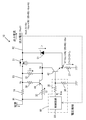
- FIG. 1 is a circuit diagram illustrating the configuration of the voltage regulator of the embodiment.
- FIG. 2 is associated with a graph showing the relationship between the output current and each voltage in the voltage regulator of the embodiment, a graph showing the relationship between the output current and each current, and a graph showing the relationship between the output current and the output voltage. It is explanatory drawing which illustrates.
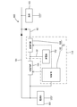
- FIG. 3 is a block diagram illustrating an electrical configuration of an in-vehicle power supply system in which the voltage regulator of the embodiment is applied to a discharge circuit.
- the collector of the first transistor is electrically connected to the collector and the control terminal of the second transistor. Then, the second transistor is energized when the control unit is in the operating state in which the operating voltage is applied to the base of the second transistor. Then, the Zener diode sets the voltage of the second conductive path to a voltage corresponding to the voltage across the Zener diode in the above operating state.
- the ground-side resistance portion is a current corresponding to the added value obtained by adding the value of the current flowing through the second resistance portion, the value of the current flowing through the third resistance portion, and the value of the current flowing through the Zener diode in the operating state. Flows. Then, the control unit stops the output of the operating voltage when the voltage of the second conductive path becomes equal to or less than the threshold value.
- the voltage regulator having the above configuration can realize a configuration in which the output can be forcibly stopped when the output current flowing through the second conductive path increases beyond the reference, while suppressing the complexity of the circuit scale.
- the main elements other than the control unit can be mainly composed of passive elements, there is a great merit in simplifying and downsizing the circuit.
- the vehicle-mounted backup power supply which is an example of the present disclosure, can be a power supply having the same effect as the above-mentioned voltage regulator by having a configuration provided with the above-mentioned voltage regulator.
- the above voltage regulator has the following actions and operations. First, when the second transistor is in the non-energized state, no current flows through the third resistor, and when the second transistor is in the energized state, the third resistor has one end of the switch on the first resistance side and a control terminal. It is desirable that a third current flows according to the potential difference between the two. Then, it is desirable that the switch is turned on when the third current flows. Then, it is desirable that the voltage at the other end of the first resistance portion is set to a value corresponding to the current flowing through the switch by interposing the first resistance portion between the first conductive path and the switch.
- the emitter is connected to the first conductive path via the second resistance portion, and the base is electrically connected to the conductive path between the first resistance portion and the switch directly or via another member. It is desirable that the first transistor is energized when the first current flowing through the first resistance portion exceeds a certain value, and the second current flows through the second resistance portion. When the first current flowing through the first resistance portion is equal to or less than a certain value, it is desirable that the first transistor is not energized and the second current does not flow through the second resistance portion. When the second transistor is energized, it is desirable that the emitter voltage of the second transistor is a fixed value based on the base voltage of the second transistor and the voltage between the base emitters.
- a fixed current based on the emitter voltage of the second transistor and the resistance value of the ground-side resistance portion flows through the ground-side resistance portion.
- the value of the fixed current is a value corresponding to the sum of the value of the second current, the value of the third current, and the value of the current flowing through the Zener diode from the cathode side to the anode side. Then, it is desirable that the current flowing through the Zener diode from the cathode side to the anode side decreases as the second current increases.
- the Zener diode breaks down. It is desirable not to do so.
- the voltage applied to the second conductive path is a value corresponding to the sum of the voltage across the Zener diode and the emitter voltage of the second transistor when a current flows from the cathode side to the anode side in the Zener diode. It is desirable that it is.
- the control unit stops the output of the operating voltage, and accordingly, the second transistor is de-energized and the switch is turned off. It is desirable to operate so as to. According to such a configuration, most or all the elements other than the control unit can be composed of passive elements, which is advantageous in terms of suppressing the circuit scale and reducing the cost.
- the voltage regulator 10 shown in FIG. 1 has a configuration in which an input voltage is input based on the power supplied through the first conductive path 91 and an output voltage is output to the second conductive path 92.
- the voltage regulator 10 includes a switch 21, a resistor (first resistor section) 31, a resistor (second resistor section) 32, a resistor (third resistor section) 33, a resistor 34, and a resistor (ground side resistor section). It has 37, a transistor (first transistor) 41, a transistor (second transistor) 42, a Zener diode 51, and a control unit 60.
- the switch 21 is configured as a P-channel MOSFET.
- the switch 21 is provided between the first conductive path 91 and the second conductive path 92.
- the source of the switch 21 is electrically connected to the third conductive path 93.
- the source of the switch 21 and the third conductive path 93 have the same potential.
- the drain of the switch 21 is electrically connected to the second conductive path 92.
- the drain of the switch 21 and the second conductive path 92 have the same potential.
- the gate (control terminal) of the switch 21 is electrically connected to the collector of the transistor 41, which will be described later, the other end of the resistor 33, and the collector of the transistor 42.
- the gate of the switch 21, the collector of the transistor 41, the other end of the resistor 33, and the collector of the transistor 42 have the same potential.
- the resistor 31 is provided between the first conductive path 91 and the third conductive path 93. One end of the resistor 31 is electrically connected to the first conductive path 91. One end of the resistor 31 and the first conductive path 91 have the same potential. One end of the resistor 31 and the first conductive path 91 have the same potential. The other end of the resistor 31 is electrically connected to the source of the switch 21 via a third conductive path 93. The other end of the resistor 31 and the third conductive path 93 have the same potential.
- the resistor 32 is provided between the first conductive path 91 and the transistor 41. One end of the resistor 32 is electrically connected to the first conductive path 91. The other end of the resistor 32 is electrically connected to the emitter of the transistor 41. The other end of the resistor 32 and the emitter of the transistor 41 have the same potential.
- the resistor 33 is provided between the first conductive path 91 and the transistor 41. One end of the resistor 33 is electrically connected to the third conductive path 93. One end of the resistor 33 and the third conductive path 93 have the same potential. The other end of the resistor 33 is electrically connected to the collector of the transistor 41, the collector of the transistor 42, and the gate of the switch 21.
- the resistor 34 is provided between the third conductive path 93 and the transistor 41. One end of the resistor 34 is electrically connected to the third conductive path 93. One end of the resistor 34 and the third conductive path 93 have the same potential. The other end of the resistor 34 is electrically connected to the base of the transistor 41. The other end of the resistor 34 and the base of the transistor 41 have the same potential.
- the transistor 41 is configured as an NPN type bipolar transistor.
- the base of the transistor 41 is electrically connected to the other end of the resistor 34.
- the emitter of the transistor 41 is electrically connected to the other end of the resistor 32.
- the collector of the transistor 41 is electrically connected to the other end of the resistor 33, the collector of the transistor 42, and the gate of the switch 21.
- the transistor 42 is configured as a PNP type bipolar transistor.
- the base of the transistor 41 is electrically connected to the other end of the resistor 35 and one end of the resistor 36, which will be described later.
- the base of the transistor 41, the other end of the resistor 35, and one end of the resistor 36 have the same potential.
- the collector of the transistor 42 is electrically connected to the collector of the transistor 41, the other end of the resistor 33, and the gate of the switch 21.
- the emitter of the transistor 42 is electrically connected to one end of a resistor 37, which will be described later, and the anode of the Zener diode 51.
- the emitter of the transistor 42, one end of the resistor 37, and the anode of the Zener diode 51 have the same potential.
- the transistor 42 is energized when the control unit 60, which will be described later, applies an operating voltage to the base.
- the control unit 60 functions to apply an operating voltage to the base of the transistor 42. It includes a control circuit 61, a resistor 35, and a resistor 36. The control unit 60 stops the output of the operating voltage when the voltage of the second conductive path 92 becomes equal to or less than the threshold value described later.
- the control circuit 61 is configured as, for example, a microcomputer, and has a memory such as a CPU, ROM, or RAM. The control circuit 61 operates based on, for example, the electric power supplied from the power source, and can operate based on the electric power from the backup power source even when the electric power supply from the power source is interrupted.
- the control circuit 61 applies an operating voltage to the base of the transistor 42 via the resistor 35.
- the control circuit 61 has a function of detecting the output voltage of the second conductive path 92.
- the resistor 35 is provided between the control circuit 61 and the transistor 42. One end of the resistor 35 is electrically connected to the output terminal of the control circuit 61. One end of the resistor 35 and the output terminal of the control circuit 61 have the same potential. The other end of the resistor 35 is electrically connected to one end of the resistor 36 and the base of the transistor 42.
- the resistor 36 is provided between the resistor 35 and the transistor 42. One end of the resistor 36 is electrically connected to the other end of the resistor 35 and the base of the transistor 42. The other end of the resistor 36 is electrically connected to the ground and is used as the ground potential.
- the resistor 37 is provided between the transistor 42 and the ground. One end of the resistor 37 is electrically connected to the emitter of the transistor 42 and the anode of the Zener diode 51. The other end of the resistor 37 is electrically connected to the ground and has a ground potential.
- the resistor 37 corresponds to an added value obtained by adding the value of the current flowing through the resistor 32, the value of the current flowing through the resistor 33, and the value of the current flowing through the Zener diode 51, which will be described later, when the transistor 42 is in the operating state. Current flows.
- the Zener diode 51 is provided between the second conductive path 92 and the resistor 37.
- the anode of the Zener diode 51 is electrically connected to the conductive path between the emitter of the transistor 42 and one end of the resistor 37.
- the cathode of the Zener diode 51 is electrically connected to the second conductive path 92.
- the cathode of the Zener diode 51 and the second conductive path 92 have the same potential.
- the Zener diode 51 sets the voltage of the second conductive path 92 to a voltage corresponding to the voltage across the two when the transistor 42 is in the operating state.
- the control unit 60 applies an operating voltage having a voltage value of Vcc to the base of the transistor 42.
- the transistor 42 is energized, and a current flows from the collector to the emitter.
- the voltage value Vout of the output voltage output from the voltage regulator 10 to the second conductive path 92 is represented by the sum V7 + Vz of the voltage value V7 of the voltage across the resistor 37 and the Zener voltage Vz of the Zener diode 51.
- the output current flowing through the second conductive path 92 increases.
- the voltage value of the power supply voltage is V
- the voltage value of the voltage applied to the third conductive path 93 is Vs
- the voltage value of the voltage across the resistor 31 is represented by VVs.
- VVs becomes as large as the voltage value Vbe of the base-emitter voltage of the transistor 41 at the timing when the output current becomes Ia shown in FIG. 2, the collector current having the current value I2 starts to flow in the transistor 41.
- the voltage value Vout of the output voltage of the second conductive path 92 is equal to or less than the threshold value (for example, a value smaller than the output voltage value Vout1 until the transistor 41 shown in FIG. 2 is energized). Is detected and the output of the operating voltage is stopped. As a result, the voltage regulator 10 can detect the overcurrent flowing through the second conductive path 92 and stop the operation.
- the power supply system 100 shown in FIG. 3 includes an in-vehicle power supply unit 101 (hereinafter, also referred to as a power supply unit 101), a backup power supply 110, a load 103, and a charging circuit 105, and supplies electric power to the load 103. It is configured as a system to get.
- the backup power supply 110 includes an in-vehicle power storage unit 102 (hereinafter, also referred to as a power storage unit 102), a control unit 60, and a discharge circuit 106.
- the power supply unit 101 functions as a main power source.
- the power storage unit 102 functions as a backup power source and becomes a power supply source when the power supply from the power supply unit 101 is interrupted.
- the power storage unit 102 is electrically connected to the first conductive path 91.
- the charging circuit 105 is a circuit that performs a charging operation to charge the power storage unit 102 based on the power supply from the power supply unit 101.
- the discharge circuit 106 is a circuit that performs a discharge operation to discharge the electric power stored in the power storage unit 102.
- the discharge circuit 106 is electrically connected to the first conductive path 91 and the second conductive path 92.
- the voltage regulator 10 is composed of the discharge circuit 106 and the control unit 60.
- the control unit 60 gives a discharge instruction signal instructing the discharge of the power storage unit 102 or a discharge stop signal instructing the discharge stop of the power storage unit 102 to the discharge circuit 106, and the discharge current is transmitted from the power storage unit 102 to the load 103.
- a discharge operation for flowing and a cutoff operation for cutting off the discharge current are performed.
- the control unit 60 transmits a discharge instruction signal according to the establishment of the backup condition. That is, the control unit 60 applies an operating voltage to the base of the transistor 42.
- the backup condition is satisfied, for example, when the voltage of the conductive path 191 drops below a predetermined threshold value.
- the discharge circuit 106 When a discharge instruction signal is given from the control unit 60, the discharge circuit 106 performs a step-down operation using the voltage of the first conductive path 91 to which the output voltage of the storage unit 102 is applied as an input voltage, and performs a step-down operation to the second output side. The discharge operation is performed so as to apply the changed output voltage to the conductive path 92.
- the discharge circuit 106 stops such a discharge operation and shuts off the second conductive path 92 and the power storage unit 102 so as to make a non-conducting state. I do.
- the discharge circuit 106 When the discharge circuit 106 is performing the discharge operation, the output current (discharge current) output from the discharge circuit 106 is supplied to the load 103.
- the voltage regulator 10 detects an overcurrent and stops the discharge operation of the discharge circuit 106 when a ground fault or the like occurs in the conductive path (second conductive path 92 or the like) between the discharge circuit 106 and the load 103. be able to.
- the collector of the transistor 41 is electrically connected to the collector of the transistor 42 and the gate of the switch 21. Then, the transistor 42 is energized when the control unit 60 is in an operating state in which an operating voltage is applied to the base of the transistor 42. Then, the Zener diode 51 sets the voltage of the second conductive path 92 to a voltage corresponding to the voltage across the Zener diode 51 in the above operating state. Then, in the resistor 37, a current corresponding to the sum of the value of the current flowing through the resistor 32, the value of the current flowing through the resistor 33, and the value of the current flowing through the Zener diode 51 in the operating state flows.
- the control unit 60 stops the output of the operating voltage when the voltage of the second conductive path 92 becomes equal to or less than the threshold value. By doing so, it is possible to realize a configuration in which the output can be forcibly stopped when the output current flowing through the second conductive path 92 increases beyond the reference, while suppressing the complexity of the circuit scale.
- the main elements other than the control unit 60 can be mainly composed of passive elements, there is a great merit in simplifying and downsizing the circuit.
- the voltage regulator 10 of the present disclosure has the following actions and operations. First, when the transistor 42 is in the non-energized state, no current flows through the resistor 33, and when the transistor 42 is in the energized state, the resistance 33 has a potential difference between one end of the switch 21 on the resistance 31 side and the gate of the switch 21. The corresponding third current flows. Then, the switch 21 is turned on when the third current flows. Then, by interposing the resistor 31 between the first conductive path 91 and the switch 21, the voltage at the other end of the resistor 31 is set to a value corresponding to the current flowing through the switch 21.
- the emitter is connected to the first conductive path 91 via the resistor 32, and the base is electrically connected to the third conductive path 93 between the resistor 31 and the switch 21 either directly or via another member.
- the transistor 41 is energized and the second current flows through the resistor 32.
- the transistor 41 is not energized and the second current does not flow through the resistor 32.
- the emitter voltage of the transistor 42 is a fixed value based on the base voltage of the transistor 42 and the voltage between the base emitters.
- the value of the fixed current is a value corresponding to the sum of the value of the second current, the value of the third current, and the value of the current flowing through the Zener diode 51 from the cathode side to the anode side. Then, the current flowing through the Zener diode 51 from the cathode side to the anode side decreases as the second current increases.
- the Zener diode 51 when the current flowing through the Zener diode 51 from the cathode side to the anode side becomes a predetermined current value or less (that is, when the voltage applied to the second conductive path 92 becomes a predetermined voltage value or less), the Zener diode 51 Is designed not to break down.
- the voltage applied to the second conductive path 92 corresponds to the sum of the voltage across the Zener diode 51 and the emitter voltage of the transistor 42 when a current flows from the cathode side to the anode side in the Zener diode 51. It is a value.
- the control unit 60 stops the output of the operating voltage, and accordingly, the transistor 42 is de-energized and the switch 21 is turned off. Operate to be in a state.
- most or all the elements other than the control unit 60 can be composed of passive elements, which is advantageous in terms of suppressing the circuit scale and reducing the cost.
- the embodiments disclosed this time are exemplary in all respects and not restrictive.
- the following embodiments can be adopted.
- the voltage value Vout of the output voltage is adjusted to a desired value by arbitrarily changing the resistance values of the resistors 35 and 36 and changing the value of the voltage applied from the control unit 60 to the base of the transistor 42. can do.
- the base of the transistor 41 is electrically connected to the other end of the resistor 34, but may be directly electrically connected to the third conductive path 93 without passing through the resistor 34.
Landscapes
- Engineering & Computer Science (AREA)
- Power Engineering (AREA)
- Radar, Positioning & Navigation (AREA)
- Automation & Control Theory (AREA)
- Physics & Mathematics (AREA)
- Electromagnetism (AREA)
- General Physics & Mathematics (AREA)
- Emergency Management (AREA)
- Business, Economics & Management (AREA)
- Continuous-Control Power Sources That Use Transistors (AREA)
- Stand-By Power Supply Arrangements (AREA)
- Charge And Discharge Circuits For Batteries Or The Like (AREA)
- Direct Current Feeding And Distribution (AREA)
Priority Applications (2)
| Application Number | Priority Date | Filing Date | Title |
|---|---|---|---|
| US17/610,969 US11709514B2 (en) | 2019-05-15 | 2020-04-27 | Voltage regulator and in-vehicle backup power supply |
| CN202080031456.8A CN113728290B (zh) | 2019-05-15 | 2020-04-27 | 电压调节器及车载用的备用电源 |
Applications Claiming Priority (2)
| Application Number | Priority Date | Filing Date | Title |
|---|---|---|---|
| JP2019091924A JP7082758B2 (ja) | 2019-05-15 | 2019-05-15 | 電圧レギュレータ及び車載用のバックアップ電源 |
| JP2019-091924 | 2019-05-15 |
Publications (2)
| Publication Number | Publication Date |
|---|---|
| WO2020230604A1 true WO2020230604A1 (ja) | 2020-11-19 |
| WO2020230604A9 WO2020230604A9 (ja) | 2021-02-25 |
Family
ID=73222859
Family Applications (1)
| Application Number | Title | Priority Date | Filing Date |
|---|---|---|---|
| PCT/JP2020/017929 Ceased WO2020230604A1 (ja) | 2019-05-15 | 2020-04-27 | 電圧レギュレータ及び車載用のバックアップ電源 |
Country Status (4)
| Country | Link |
|---|---|
| US (1) | US11709514B2 (enExample) |
| JP (1) | JP7082758B2 (enExample) |
| CN (1) | CN113728290B (enExample) |
| WO (1) | WO2020230604A1 (enExample) |
Cited By (1)
| Publication number | Priority date | Publication date | Assignee | Title |
|---|---|---|---|---|
| JP7558468B1 (ja) * | 2024-02-29 | 2024-09-30 | 三菱電機株式会社 | 電源回路 |
Families Citing this family (1)
| Publication number | Priority date | Publication date | Assignee | Title |
|---|---|---|---|---|
| EP4014101A4 (en) * | 2019-08-13 | 2023-05-10 | Saab Ab | CIRCUIT ARRANGEMENT WITH ADJUSTABLE ZENER VOLTAGE |
Citations (2)
| Publication number | Priority date | Publication date | Assignee | Title |
|---|---|---|---|---|
| JPH11305855A (ja) * | 1998-04-27 | 1999-11-05 | Mitsubishi Electric Corp | 電源装置 |
| JP2010055450A (ja) * | 2008-08-29 | 2010-03-11 | Kenwood Corp | 定電圧回路 |
Family Cites Families (12)
| Publication number | Priority date | Publication date | Assignee | Title |
|---|---|---|---|---|
| US3626278A (en) * | 1969-03-12 | 1971-12-07 | Hitachi Ltd | Collector follower-type transistorized voltage regulator |
| US3697861A (en) * | 1971-04-29 | 1972-10-10 | Collins Radio Co | Short circuit protected voltage regulator |
| US5563500A (en) * | 1994-05-16 | 1996-10-08 | Thomson Consumer Electronics, Inc. | Voltage regulator having complementary type transistor |
| JP3282378B2 (ja) * | 1994-06-24 | 2002-05-13 | 松下電工株式会社 | パワー素子駆動保護回路及びmosfet駆動保護回路 |
| US5773965A (en) * | 1995-10-24 | 1998-06-30 | Rohm Co., Ltd. | Switching power supply apparatus for converting a high DC voltage into a low DC voltage |
| JP3112069B2 (ja) * | 1997-03-24 | 2000-11-27 | エヌイーシーワイヤレスネットワークス株式会社 | 電圧安定化回路 |
| JP2005198439A (ja) | 2004-01-08 | 2005-07-21 | Matsushita Electric Ind Co Ltd | Ldo出力ショート保護システム |
| JP4597596B2 (ja) * | 2004-07-13 | 2010-12-15 | パイオニア株式会社 | 車両用電源装置 |
| US7205752B2 (en) * | 2004-09-07 | 2007-04-17 | Flextronics Ap, Llc | Master-slave critical conduction mode power converter |
| CN100533327C (zh) * | 2006-05-29 | 2009-08-26 | 华硕电脑股份有限公司 | 具有过电流保护的电压调节电路 |
| US8779735B2 (en) * | 2011-03-15 | 2014-07-15 | Infineon Technologies Ag | System and method for an overcurrent protection and interface circuit between an energy source and a load |
| JP6812935B2 (ja) * | 2017-09-20 | 2021-01-13 | 株式会社オートネットワーク技術研究所 | 車載用判定回路及び車載用電源装置 |
-
2019
- 2019-05-15 JP JP2019091924A patent/JP7082758B2/ja active Active
-
2020
- 2020-04-27 US US17/610,969 patent/US11709514B2/en active Active
- 2020-04-27 CN CN202080031456.8A patent/CN113728290B/zh active Active
- 2020-04-27 WO PCT/JP2020/017929 patent/WO2020230604A1/ja not_active Ceased
Patent Citations (2)
| Publication number | Priority date | Publication date | Assignee | Title |
|---|---|---|---|---|
| JPH11305855A (ja) * | 1998-04-27 | 1999-11-05 | Mitsubishi Electric Corp | 電源装置 |
| JP2010055450A (ja) * | 2008-08-29 | 2010-03-11 | Kenwood Corp | 定電圧回路 |
Cited By (2)
| Publication number | Priority date | Publication date | Assignee | Title |
|---|---|---|---|---|
| JP7558468B1 (ja) * | 2024-02-29 | 2024-09-30 | 三菱電機株式会社 | 電源回路 |
| WO2025182038A1 (ja) * | 2024-02-29 | 2025-09-04 | 三菱電機株式会社 | 回路、電圧補償回路、電源回路、および、レベルシフト回路 |
Also Published As
| Publication number | Publication date |
|---|---|
| CN113728290A (zh) | 2021-11-30 |
| US20220229454A1 (en) | 2022-07-21 |
| US11709514B2 (en) | 2023-07-25 |
| CN113728290B (zh) | 2022-12-09 |
| WO2020230604A9 (ja) | 2021-02-25 |
| JP7082758B2 (ja) | 2022-06-09 |
| JP2020187560A (ja) | 2020-11-19 |
Similar Documents
| Publication | Publication Date | Title |
|---|---|---|
| US10955866B2 (en) | Voltage regulator | |
| US8502513B2 (en) | Voltage regulator | |
| US11031771B2 (en) | Power supply control apparatus | |
| US7061302B2 (en) | Semiconductor integrated circuit device | |
| US10761549B2 (en) | Voltage sensing mechanism to minimize short-to-ground current for low drop-out and bypass mode regulators | |
| US10654428B2 (en) | Power supply control device | |
| JP5667946B2 (ja) | ハイサイドスイッチ回路 | |
| US10135234B2 (en) | Preventive apparatus | |
| US9531261B2 (en) | Power supply control device | |
| JP7082758B2 (ja) | 電圧レギュレータ及び車載用のバックアップ電源 | |
| JP2010193033A (ja) | 過電流保護回路 | |
| US11841721B2 (en) | Voltage regulator and in-vehicle backup power supply | |
| JP2001238347A (ja) | 電源制御回路 | |
| US20250015797A1 (en) | Control device | |
| US10599198B2 (en) | Load driving device | |
| CN112368907A (zh) | 电路装置 | |
| JP2009240007A (ja) | 電源回路 | |
| US11870427B2 (en) | Power supply control device | |
| JP2018101882A (ja) | 出力ドライバ回路 | |
| KR100828260B1 (ko) | 역 접속 전원 차단 회로 및 이를 포함하는 모터 회로 | |
| JP2002312040A (ja) | 負荷制御装置 |
Legal Events
| Date | Code | Title | Description |
|---|---|---|---|
| 121 | Ep: the epo has been informed by wipo that ep was designated in this application |
Ref document number: 20804897 Country of ref document: EP Kind code of ref document: A1 |
|
| NENP | Non-entry into the national phase |
Ref country code: DE |
|
| 122 | Ep: pct application non-entry in european phase |
Ref document number: 20804897 Country of ref document: EP Kind code of ref document: A1 |