WO2020213232A1 - Cu合金ターゲット - Google Patents
Cu合金ターゲット Download PDFInfo
- Publication number
- WO2020213232A1 WO2020213232A1 PCT/JP2020/004644 JP2020004644W WO2020213232A1 WO 2020213232 A1 WO2020213232 A1 WO 2020213232A1 JP 2020004644 W JP2020004644 W JP 2020004644W WO 2020213232 A1 WO2020213232 A1 WO 2020213232A1
- Authority
- WO
- WIPO (PCT)
- Prior art keywords
- film
- alloy
- cap
- cap film
- main body
- Prior art date
- Legal status (The legal status is an assumption and is not a legal conclusion. Google has not performed a legal analysis and makes no representation as to the accuracy of the status listed.)
- Ceased
Links
Images


Classifications
-
- C—CHEMISTRY; METALLURGY
- C22—METALLURGY; FERROUS OR NON-FERROUS ALLOYS; TREATMENT OF ALLOYS OR NON-FERROUS METALS
- C22C—ALLOYS
- C22C9/00—Alloys based on copper
- C22C9/01—Alloys based on copper with aluminium as the next major constituent
-
- C—CHEMISTRY; METALLURGY
- C23—COATING METALLIC MATERIAL; COATING MATERIAL WITH METALLIC MATERIAL; CHEMICAL SURFACE TREATMENT; DIFFUSION TREATMENT OF METALLIC MATERIAL; COATING BY VACUUM EVAPORATION, BY SPUTTERING, BY ION IMPLANTATION OR BY CHEMICAL VAPOUR DEPOSITION, IN GENERAL; INHIBITING CORROSION OF METALLIC MATERIAL OR INCRUSTATION IN GENERAL
- C23C—COATING METALLIC MATERIAL; COATING MATERIAL WITH METALLIC MATERIAL; SURFACE TREATMENT OF METALLIC MATERIAL BY DIFFUSION INTO THE SURFACE, BY CHEMICAL CONVERSION OR SUBSTITUTION; COATING BY VACUUM EVAPORATION, BY SPUTTERING, BY ION IMPLANTATION OR BY CHEMICAL VAPOUR DEPOSITION, IN GENERAL
- C23C14/00—Coating by vacuum evaporation, by sputtering or by ion implantation of the coating forming material
- C23C14/22—Coating by vacuum evaporation, by sputtering or by ion implantation of the coating forming material characterised by the process of coating
- C23C14/34—Sputtering
- C23C14/3407—Cathode assembly for sputtering apparatus, e.g. Target
-
- C—CHEMISTRY; METALLURGY
- C22—METALLURGY; FERROUS OR NON-FERROUS ALLOYS; TREATMENT OF ALLOYS OR NON-FERROUS METALS
- C22C—ALLOYS
- C22C9/00—Alloys based on copper
- C22C9/06—Alloys based on copper with nickel or cobalt as the next major constituent
-
- C—CHEMISTRY; METALLURGY
- C22—METALLURGY; FERROUS OR NON-FERROUS ALLOYS; TREATMENT OF ALLOYS OR NON-FERROUS METALS
- C22C—ALLOYS
- C22C9/00—Alloys based on copper
- C22C9/10—Alloys based on copper with silicon as the next major constituent
-
- C—CHEMISTRY; METALLURGY
- C23—COATING METALLIC MATERIAL; COATING MATERIAL WITH METALLIC MATERIAL; CHEMICAL SURFACE TREATMENT; DIFFUSION TREATMENT OF METALLIC MATERIAL; COATING BY VACUUM EVAPORATION, BY SPUTTERING, BY ION IMPLANTATION OR BY CHEMICAL VAPOUR DEPOSITION, IN GENERAL; INHIBITING CORROSION OF METALLIC MATERIAL OR INCRUSTATION IN GENERAL
- C23C—COATING METALLIC MATERIAL; COATING MATERIAL WITH METALLIC MATERIAL; SURFACE TREATMENT OF METALLIC MATERIAL BY DIFFUSION INTO THE SURFACE, BY CHEMICAL CONVERSION OR SUBSTITUTION; COATING BY VACUUM EVAPORATION, BY SPUTTERING, BY ION IMPLANTATION OR BY CHEMICAL VAPOUR DEPOSITION, IN GENERAL
- C23C14/00—Coating by vacuum evaporation, by sputtering or by ion implantation of the coating forming material
- C23C14/22—Coating by vacuum evaporation, by sputtering or by ion implantation of the coating forming material characterised by the process of coating
- C23C14/34—Sputtering
-
- G—PHYSICS
- G02—OPTICS
- G02F—OPTICAL DEVICES OR ARRANGEMENTS FOR THE CONTROL OF LIGHT BY MODIFICATION OF THE OPTICAL PROPERTIES OF THE MEDIA OF THE ELEMENTS INVOLVED THEREIN; NON-LINEAR OPTICS; FREQUENCY-CHANGING OF LIGHT; OPTICAL LOGIC ELEMENTS; OPTICAL ANALOGUE/DIGITAL CONVERTERS
- G02F1/00—Devices or arrangements for the control of the intensity, colour, phase, polarisation or direction of light arriving from an independent light source, e.g. switching, gating or modulating; Non-linear optics
- G02F1/01—Devices or arrangements for the control of the intensity, colour, phase, polarisation or direction of light arriving from an independent light source, e.g. switching, gating or modulating; Non-linear optics for the control of the intensity, phase, polarisation or colour
- G02F1/13—Devices or arrangements for the control of the intensity, colour, phase, polarisation or direction of light arriving from an independent light source, e.g. switching, gating or modulating; Non-linear optics for the control of the intensity, phase, polarisation or colour based on liquid crystals, e.g. single liquid crystal display cells
- G02F1/133—Constructional arrangements; Operation of liquid crystal cells; Circuit arrangements
- G02F1/1333—Constructional arrangements; Manufacturing methods
- G02F1/1343—Electrodes
-
- G—PHYSICS
- G02—OPTICS
- G02F—OPTICAL DEVICES OR ARRANGEMENTS FOR THE CONTROL OF LIGHT BY MODIFICATION OF THE OPTICAL PROPERTIES OF THE MEDIA OF THE ELEMENTS INVOLVED THEREIN; NON-LINEAR OPTICS; FREQUENCY-CHANGING OF LIGHT; OPTICAL LOGIC ELEMENTS; OPTICAL ANALOGUE/DIGITAL CONVERTERS
- G02F1/00—Devices or arrangements for the control of the intensity, colour, phase, polarisation or direction of light arriving from an independent light source, e.g. switching, gating or modulating; Non-linear optics
- G02F1/01—Devices or arrangements for the control of the intensity, colour, phase, polarisation or direction of light arriving from an independent light source, e.g. switching, gating or modulating; Non-linear optics for the control of the intensity, phase, polarisation or colour
- G02F1/13—Devices or arrangements for the control of the intensity, colour, phase, polarisation or direction of light arriving from an independent light source, e.g. switching, gating or modulating; Non-linear optics for the control of the intensity, phase, polarisation or colour based on liquid crystals, e.g. single liquid crystal display cells
- G02F1/133—Constructional arrangements; Operation of liquid crystal cells; Circuit arrangements
- G02F1/136—Liquid crystal cells structurally associated with a semi-conducting layer or substrate, e.g. cells forming part of an integrated circuit
- G02F1/1362—Active matrix addressed cells
- G02F1/1368—Active matrix addressed cells in which the switching element is a three-electrode device
-
- H—ELECTRICITY
- H10—SEMICONDUCTOR DEVICES; ELECTRIC SOLID-STATE DEVICES NOT OTHERWISE PROVIDED FOR
- H10D—INORGANIC ELECTRIC SEMICONDUCTOR DEVICES
- H10D30/00—Field-effect transistors [FET]
- H10D30/60—Insulated-gate field-effect transistors [IGFET]
- H10D30/67—Thin-film transistors [TFT]
-
- H—ELECTRICITY
- H10—SEMICONDUCTOR DEVICES; ELECTRIC SOLID-STATE DEVICES NOT OTHERWISE PROVIDED FOR
- H10D—INORGANIC ELECTRIC SEMICONDUCTOR DEVICES
- H10D64/00—Electrodes of devices having potential barriers
- H10D64/01—Manufacture or treatment
- H10D64/011—Manufacture or treatment of electrodes ohmically coupled to a semiconductor
-
- H—ELECTRICITY
- H10—SEMICONDUCTOR DEVICES; ELECTRIC SOLID-STATE DEVICES NOT OTHERWISE PROVIDED FOR
- H10D—INORGANIC ELECTRIC SEMICONDUCTOR DEVICES
- H10D64/00—Electrodes of devices having potential barriers
- H10D64/20—Electrodes characterised by their shapes, relative sizes or dispositions
- H10D64/27—Electrodes not carrying the current to be rectified, amplified, oscillated or switched, e.g. gates
-
- H—ELECTRICITY
- H10—SEMICONDUCTOR DEVICES; ELECTRIC SOLID-STATE DEVICES NOT OTHERWISE PROVIDED FOR
- H10D—INORGANIC ELECTRIC SEMICONDUCTOR DEVICES
- H10D64/00—Electrodes of devices having potential barriers
- H10D64/60—Electrodes characterised by their materials
- H10D64/66—Electrodes having a conductor capacitively coupled to a semiconductor by an insulator, e.g. MIS electrodes
-
- H—ELECTRICITY
- H10—SEMICONDUCTOR DEVICES; ELECTRIC SOLID-STATE DEVICES NOT OTHERWISE PROVIDED FOR
- H10P—GENERIC PROCESSES OR APPARATUS FOR THE MANUFACTURE OR TREATMENT OF DEVICES COVERED BY CLASS H10
- H10P14/00—Formation of materials, e.g. in the shape of layers or pillars
- H10P14/40—Formation of materials, e.g. in the shape of layers or pillars of conductive or resistive materials
- H10P14/42—Formation of materials, e.g. in the shape of layers or pillars of conductive or resistive materials using a gas or vapour
-
- H—ELECTRICITY
- H10—SEMICONDUCTOR DEVICES; ELECTRIC SOLID-STATE DEVICES NOT OTHERWISE PROVIDED FOR
- H10P—GENERIC PROCESSES OR APPARATUS FOR THE MANUFACTURE OR TREATMENT OF DEVICES COVERED BY CLASS H10
- H10P14/00—Formation of materials, e.g. in the shape of layers or pillars
- H10P14/40—Formation of materials, e.g. in the shape of layers or pillars of conductive or resistive materials
- H10P14/42—Formation of materials, e.g. in the shape of layers or pillars of conductive or resistive materials using a gas or vapour
- H10P14/44—Physical vapour deposition [PVD]
- H10P14/45—Sputtering
-
- H—ELECTRICITY
- H10—SEMICONDUCTOR DEVICES; ELECTRIC SOLID-STATE DEVICES NOT OTHERWISE PROVIDED FOR
- H10D—INORGANIC ELECTRIC SEMICONDUCTOR DEVICES
- H10D64/00—Electrodes of devices having potential barriers
- H10D64/20—Electrodes characterised by their shapes, relative sizes or dispositions
- H10D64/23—Electrodes carrying the current to be rectified, amplified, oscillated or switched, e.g. sources, drains, anodes or cathodes
Definitions
- the present invention relates to the field of wiring film used for minute semiconductor devices, and particularly to the technical field of electrode layer and wiring film in contact with a substrate.
- Si oxide thin film that serves as a gate insulating film for the TFT on a large area substrate ( It is necessary to form a Si oxide thin film that serves as a protective film for SiO x ) or TFT.
- the Si oxide thin film used for the gate insulating film and the protective film is formed on the substrate on which the wiring film has already been formed, a CVD method capable of forming a film at a low temperature is used, but the performance and protection of the TFT are used. In order to improve the characteristics of the film, it is desirable to raise the formation temperature of the Si oxide thin film by CVD as high as possible.
- Si diffuses into the wiring film, and peeling occurs between the Si oxide thin film and the wiring film.
- the present invention was created to solve the above-mentioned inconveniences of the prior art, and an object thereof is a wiring film having high adhesion to a Si oxide thin film, a Cu alloy target for forming the wiring film, and a Cu alloy target.
- An object of the present invention is to provide a semiconductor element in which the wiring film is used.
- the present invention is a Cu alloy target composed of a Cap film alloy, and when the number of atoms of the Cap film alloy is 100 at%, the Cap film alloy contains Cu exceeding 50 at% and an additive metal.
- 0.5 at% or more of Al and the added metal is made of three kinds of metal materials composed of 0.5 at% or more of Mg, 0.5 at% or more of Si, and 3 at% or more of Ni.
- it is a Cu alloy target containing at least one kind of metal material.
- the present invention is a Cu alloy target in which the additive metal is Mg of 0.5 at% or more and less than 7 at%.
- the additive metal is a Cu alloy target in which Si is 0.5 at% or more and less than 15 at%.
- the additive metal is a Cu alloy target in which Ni is 3 at% or more and less than 50 at%.
- the present invention is a Cu alloy target composed of a Cap film alloy, and when the number of atoms of the Cap film alloy is 100 at%, the Cap film alloy contains Cu exceeding 50 at% and 0. It is a Cu alloy target containing 5 at% or more of Ca.
- the wiring film can be patterned by a single etching.
- Sectional drawing for demonstrating the semiconductor device of an example of this invention and the liquid crystal display device of an example of this invention.
- A)-(c) Cross-sectional view (1) for explaining the manufacturing process of the semiconductor device of the example of the present invention and the liquid crystal display device of the present invention.
- A)-(c) Cross-sectional view (2) for explaining the manufacturing process of the semiconductor device of the example of the present invention and the liquid crystal display device of the present invention.
- Cross-sectional view (4) for explaining the manufacturing process of the semiconductor device of one example of the present invention and the liquid crystal display device of one example of the present invention.
- Reference numeral 2 in FIG. 1 is a liquid crystal display device according to an embodiment of the present invention, and a cross-sectional view of TFT 11 of the first example of the present invention is shown.
- the TFT 11 has a gate electrode film 32.
- the gate electrode film 32 is elongated and is arranged on the surface of a substrate 31 made of either one or both of glass and resin.
- the material constituting the substrate 31 also includes a substrate formed of a material composed of a resin and glass as a result of containing glass fibers in the resin.
- a gate insulating film 33 made of Si oxide (SiO x ) is arranged on the gate electrode film 32 at least in the width direction.
- a semiconductor layer 34 is arranged on the gate insulating film 33 with a length protruding from the gate electrode film 32 on both ends in the width direction of the gate electrode film 32, and the gate electrode film 32 has one end and the other end of the semiconductor layer 34.
- the source electrode film 51 is arranged on one side of the semiconductor layer 34, and the drain electrode film 52 is arranged on the other side.
- a recess 55 is provided between the source electrode film 51 and the drain electrode film 52, and the source electrode film 51 and the drain electrode film 52 are electrically separated by the recess 55, and the source electrode film 51 and the drain electrode film are separated from each other. Different voltages can be applied between 52.
- a protective insulating film 41 made of Si oxide is formed on the source electrode film 51, the drain electrode film 52, and the recess 55 between them, and the protective insulating film 41 is used here as a protective film. ing.
- the portion of the semiconductor layer 34 in contact with the source electrode film 51 and its periphery is designated as the source region 71
- the portion in contact with the drain electrode film 52 and its periphery is designated as the drain region 72
- the source region 71 and the drain region 72 Assuming that the space is the channel region 73, when a gate voltage is applied to the gate electrode film 32 while a voltage is applied between the source electrode film 51 and the drain electrode film 52 to form a channel layer in the channel region 73, the source region 71 is formed. And the drain region 72 are connected by a channel layer with low resistance, and as a result, the source electrode film 51 and the drain electrode film 52 are electrically connected, and the TFT 11 is conducted.
- the polarity of the semiconductor in the channel region 73 is the same as the polarity of the semiconductor in the source region 71 and the polarity of the semiconductor in the drain region 72, and the polarity of the channel layer is the same as the polarity of the semiconductor in the channel region 73.
- the polarity of the semiconductor in the channel region 73 is different from the polarity of the semiconductor in the source region 71 and the polarity of the semiconductor in the drain region 72, and the polarity of the channel layer is the polarity of the semiconductor in the source region 71 and the polarity of the semiconductor in the drain region 72.
- the case where the polarities are the same is also included in the present invention.
- the channel layer disappears, the source electrode film 51 and the drain electrode film 52 become high resistance, and are electrically separated.
- a pixel electrode 82 is arranged on the liquid crystal display unit 12, and a liquid crystal 83 is arranged on the pixel electrode 82.
- the upper electrode 81 is located on the liquid crystal 83, and when a voltage is applied between the pixel electrode 82 and the upper electrode 81, the polarization property of the light passing through the liquid crystal 83 is changed, and a polarizing filter (not shown). Light transmission is controlled.
- the pixel electrode 82 is electrically connected to the source electrode film 51 and the drain electrode film 52 (here, the drain electrode film 52), and when the TFT 11 is turned ON / OFF, the voltage application to the pixel electrode 82 is started / ended. Is done.
- the pixel electrode 82 is composed of a part of the transparent conductive layer 42 connected to the drain electrode film 52.
- the transparent conductive layer 42 is made of, for example, ITO.
- a wiring film 35 is arranged below the transparent conductive layer 42.
- the wiring film 35 and the gate electrode film 32 each have a low-resistance main body film 39 and a Cap film 38 arranged on the main body film 39 and having a higher resistance than the main body film 39.
- Both the source electrode film 51 and the drain electrode film 52 have a low-resistance main body film 49 and a Cap film 48 that is arranged on the main body film 49 and has a higher resistance than the main body film 49.
- reference numeral 80 is a sputtering device, and the sputtering device 80 connects the gate electrode film 32 and the wiring film 35, and the source electrode film 51 and the drain electrode film 52. It shall be formed.
- the sputtering apparatus 80 has a vacuum chamber 89, and first to third cathode electrodes 86a to 86c are arranged inside the vacuum chamber 89, and the first cathode electrode 86a is an alloy for an adhesion layer.
- a first target 88a made of is arranged, a second target 88b made of pure copper is arranged on the second cathode electrode 86b, and a Cu alloy target 88c made of a cap film alloy is arranged on the third cathode electrode 86c. Is placed.
- the Cu alloy target 88c is a Cu alloy target composed of an alloy for a Cap film, and is a Cu alloy target formed by an alloy for a Cap film containing an aluminum atom (Al) and an alloy for a Cap film containing a calcium atom (Ca).
- Al aluminum atom
- Ca calcium atom
- the Al-containing cap film alloy contains copper atoms (Cu) exceeding 50 at%, an additive metal, and 0.5 at% or more of Al when the number of atoms of the Cap film alloy is 100 at%.
- the added metals are three kinds of metals composed of 0.5 at% or more of magnesium atom (Mg), 0.5 at% or more of silicon atom (Si), and 3 at% or more of nickel atom (Ni). Among the materials, it contains at least one kind of metallic material.
- the Ca-containing cap film alloy is a Cu alloy target containing more than 50 at% Cu and 0.5 at% or more Ca when the number of atoms of the Cap film alloy is 100 at%.
- a Cu alloy target formed by molding one of the two types of Cap film alloys is arranged inside the vacuum chamber 89 of the sputtering apparatus 80 as a Cu alloy target 88c.
- the vacuum chamber 89 is evacuated by the vacuum exhaust device 86, and at the time of sputtering, a sputtering gas composed of a rare gas such as Ar gas is introduced into the inside of the vacuum chamber 89 from the gas source 87, and the first to third are used.
- Sputtering voltage is applied to the first to third cathode electrodes 86a to 86c by the sputtering power supplies 85a to 85c of the above, and sputtering of the first target 88a, the second target 88b, and the Cu alloy target 88c is started.
- the substrate 31 is carried into the vacuum chamber 89, the substrate 31 which is the object of film formation is carried into the inside of the vacuum chamber 89 of the sputtering apparatus 80, and the carried-in substrate 31 is used as the first and second targets 88a and 88b. They face each other in this order, a close contact layer is formed by sputtering the first target 88a, a low resistance layer is formed on the close contact layer by sputtering the second target 88b, and the close contact layer and the low resistance layer are formed on the substrate 31. It forms a main body film which is a low resistance layer having a two-layer structure composed of two layers.
- the substrate 31 on which the main body film is formed is sputtered with the Cu alloy target 88c to form a Cap film on the main body film.
- the Cap film contacts the low resistance layer.
- Reference numeral 36 in FIG. 2A indicates an adhesion layer
- reference numeral 37 indicates a low resistance layer
- reference numeral 39 indicates a main body film
- Reference numeral 38 indicates a Cap film.
- oxygen gas or a gas having an oxygen atom in the chemical structure is not introduced into the vacuum chamber 89, and oxygen is not contained in the thin films 36 to 38. There is.
- the substrate 31 on which the patterned resist film 44 is formed on the Cap film 38 and the main body film 39 and the Cap film 38 are formed is used as an etching solution for etching Cu.
- the Cap film 38 in the portion exposed between the resist film 44 and the resist film 44 is etched with the same etching solution, and then the main body film 39 in the portion exposed by etching the Cap film 38 presses the Cap film 38. It is etched by the same etching solution as the etched etching solution.
- FIG. 2C shows the state, the main body film 39 and the Cap film 38 are partially removed, and the gate electrode film 32 and the wiring film 35 are formed on the substrate 31 by the remaining portion. ..
- the surface of the substrate 31 other than the portion where the gate electrode film 32 and the wiring film 35 are located is exposed.
- the substrate 31 is carried into the CVD apparatus, and the substrate 31 is brought into the CVD apparatus at 200 ° C. or higher and 350 ° C. or higher.
- the temperature is raised to °C or less, silane gas is introduced as a raw material gas into the CVD apparatus, oxygen gas is introduced as a reaction gas, and argon gas is introduced as a diluting gas, and the raw material gas and the reaction gas are chemically vapor deposition. React (CVD method).
- Si oxide When Si oxide is generated by the chemical reaction, Si oxide is deposited on the surface of the substrate 31, the surface of the gate electrode film 32, and the surface of the wiring film 35, as shown in FIG. 3A. , A gate insulating film 33 made of a Si oxide thin film is formed.
- the substrate 31 is moved to another film forming apparatus, a thin film made of a semiconductor material (for example, Si semiconductor or an oxide semiconductor) is formed on the gate insulating film 33, and the thin film is patterned on the gate insulating film 33.
- the semiconductor layer 34 as shown in 3 (b) is formed.
- the substrate 31 on which the semiconductor layer 34 is formed is carried into the vacuum chamber 89 of the sputtering apparatus 80, and the first target 88a, the second target 88b, and the Cu alloy target 88c are sputtered, and FIG. 3 (c) ),
- the adhesion layer 46 is formed on the semiconductor layer 34
- the low resistance layer 47 is formed on the adhesion layer 46
- the main body film 49 composed of the adhesion layer 46 and the low resistance layer 47 is obtained.
- a Cap film 48 is formed on the main body film 49.
- the Cap film 48 comes into contact with the low resistance layer 47.
- the metal layer composed of the main body film 49 and the Cap film 48 is patterned to form the source electrode film 51 and the drain electrode film 52 as shown in FIG. 4A.
- the source electrode film 51 and the drain electrode film 52 have a main body film 49 and a cap film 48, respectively, the source electrode film 51 contacts the source region 71, and the drain electrode film 52 contacts the drain region 72. ..
- the source electrode film 51 and the drain electrode film 52 are located on one side of the semiconductor layer 34 in the width direction and on the opposite side, and are in contact with the gate electrode film 32 and the gate electrode film 32 in between. 33 is located.
- the substrate 31 in this state is carried into the CVD device, the temperature of the substrate 31 is raised to 250 ° C. or higher and 350 ° C. or lower, silane gas is used as a raw material gas, oxygen gas is used as a reaction gas, and argon gas is used inside the CVD device. It is introduced as a diluting gas, Si oxide is deposited by a CVD method, and patterning is performed to obtain a protective insulating film 41 made of Si oxide as shown in FIG. 4 (b).
- a connection hole 43 used as a via hole, a contact hole, or the like is formed in the protective insulating film 41 by patterning, and a drain electrode film 52, a source electrode film 51, a wiring film 35, or the like is formed on the bottom surface of the connection hole 43.
- the surfaces of the cap films 38 and 48 to be provided are exposed, and a patterned transparent conductive layer is formed on the protective insulating film 41 in that state.
- Reference numeral 42 in FIG. 5 is a patterned transparent conductive layer
- reference numeral 82 is a pixel electrode composed of the transparent conductive layer 42.
- the liquid crystal display device 2 shown in FIG. 1 is obtained.
- a gate insulating film 33 made of Si oxide is formed on the surface of the gate electrode film 32 and the surface of the wiring film 35 by the CVD method, and the surface of the drain electrode film 52 and the source are formed.
- a protective insulating film 41 made of Si oxide is formed on the surface of the electrode film 51 by the CVD method.
- the protective insulating film 41 and the gate insulating film 33 are in contact with the Cap films 38 and 48, and the oxidation of Cu in the Cap films 38 and 48 and the diffusion of Si into the Cap films 38 and 48 are prevented.
- the peeling between the gate insulating film 33 and the gate electrode film 32 and the wiring film 35 and the peeling between the protective insulating film 41 and the source electrode film 51 and the drain electrode film 52 are prevented.
- the first and second targets made of Cu alloy or pure Cu are sputtered to form a main body film made of an adhesion layer and a low resistance layer on the surface of a glass substrate, and then Cu arranged in the sputtering apparatus 80.
- the alloy target was sputtered to form a Cap film on the main body film, and a wiring film composed of the main body film and the Cap film was obtained.
- the temperature of the glass substrate on which the wiring film was formed was raised, the raw material gas, oxygen gas, and dilution gas were introduced and chemically reacted, and an insulating film made of Si oxide was formed on the Cap film in contact with the Cap film. ..
- a two-layer film consisting of a wiring film and an insulating film on a glass substrate is cut into a 1 cm ⁇ 1 cm square to form 100 square squares consisting of small pieces of the two-layer film, and adhesive tape is attached to each square. Then, the adhesive tape was peeled off from the bilayer film.
- ⁇ Cu-Al-Mg> When the number of atoms of the Cap film alloy is 100 at%, Al is contained in the range of 0 at% or more and 25 at% or less, and Mg, which is a metal material, is contained in the range of 0.5 at% or more and 7 at% or less as an additive metal.
- a Cu alloy target is produced by producing a contained alloy for a Cap film, a Cap film is formed on the main body film by sputtering, and an insulating film is formed on the Cap film by a CVD method in a temperature range of 200 ° C. or higher and 350 ° C. or lower. It was formed and a peeling test was performed.
- Table 1 below shows the film formation conditions consisting of the Al content, Mg content, and CVD temperature, and the peeling test results corresponding to each film formation condition.
- the Cap film contains 0.5 at% or more of Al and 0.5 at% or more of Mg because all of them are good products.
- Mg may be contained in the range of less than 7 at%, but it is not limited to less than 7 at% because there is a possibility that a Cu alloy target can be formed even if it is 7 at% or more.
- Table 2 below shows the film formation conditions consisting of the Al content and Si content and the CVD temperature, and the peeling test results corresponding to each film formation condition.
- Al is contained in an amount of 0.5 at% or more and Si is contained in an amount of 0.5 at% or more because all of them are good products.
- Si When Al is contained in an amount of 25 at% or more, or when Si is contained in an amount of 15 at% or more, a Cu alloy target cannot be created by the current technology. Therefore, Si may be contained in a range of less than 15 at%, but it is not limited to a range of less than 15 at% because there is a possibility that a Cu alloy target can be formed even if it is 15 at% or more.
- ⁇ Cu-Al-Ni> When the number of atoms of the cap film alloy is 100 at%, Al is contained in the range of 0 at% or more and 25 at% or less, and Ni, which is a metal material, is contained in the range of 3 at% or more and 50 at% or less as an additive metal.
- a cap film alloy is produced to produce a Cu alloy target, a cap film is formed on the main body film by sputtering, and an insulating film is formed on the cap film by a CVD method in a temperature range of 200 ° C. or higher and 350 ° C. or lower. , A peeling test was performed.
- Table 3 shows the film forming conditions consisting of the Al content and Ni content and the CVD temperature, and the peeling test results corresponding to each film forming condition.
- Al is contained in an amount of 0.5 at% or more and Ni is contained in an amount of 3 at% or more because all of them are good products.
- Ni when Al is contained in an amount of 25 at% or more, or when Ni is contained in an amount of 50 at% or more, a Cu alloy target cannot be created by the current technology. Therefore, Ni may be contained in a range of less than 50 at%.
- ⁇ Cu-Ca> When the number of atoms of the Cap film alloy is 100 at%, a Cap film alloy containing Ca, which is a metal material, in the range of 0 at% or more and 10 at% or less is produced as an additive metal to manufacture a Cu alloy target. Then, a Cap film was formed on the main body film by sputtering, and an insulating film was formed on the Cap film by a CVD method in a temperature range of 200 ° C. or higher and 350 ° C. or lower, and a peeling test was performed.
- Table 4 below shows the film formation conditions consisting of the Cu content and the CVD temperature and the peeling test results corresponding to each film formation condition.
- Ca is contained in an amount of 0.5 at% or more because all of them are good products.
- Ca is contained in an amount of 7 at% or more, a Cu alloy target cannot be created with the current technology. Therefore, Ca may be contained in a range of less than 7 at%, but it is not limited to a range of less than 7 at% because a Cu alloy target may be formed even if it is contained in an amount of 7 at% or more.
- ⁇ Cu-Al> As a comparative example, when the number of atoms of the Cap film alloy is 100 at%, a Cap film alloy containing Al in the range of 0 at% or more and 25 at% or less is prepared to produce a Cu alloy target, and the Cu alloy target is manufactured by sputtering. A Cap film was formed on the main body film, an insulating film was formed on the Cap film by a CVD method in a temperature range of 200 ° C. or higher and 350 ° C. or lower, and a peeling test was performed.
- Table 5 shows the film forming conditions consisting of the Al content and the CVD temperature and the peeling test results corresponding to each film forming condition.
- the Cu alloy target composed of the Cap film alloy contains Cu exceeding 50 at%, an additive metal, and Al of 0.5 at% or more when the number of atoms of the Cap film alloy is 100 at%.
- the added metal contains at least one of three types of metal materials composed of 0.5 at% or more of Mg, 0.5 at% or more of Si, and 3 at% or more of Ni. Good.
- the Cu alloy target composed of the Cap film alloy contains Cu exceeding 50 at% and Ca of 0.5 at% or more. It may be contained.
- the composition of the Cap film obtained by sputtering the Cu alloy target is the same as the composition of the Cu alloy target, and in the semiconductor element, the wiring film having the above composition is a gate electrode film, a source electrode film, a drain electrode film, or the like. It can be used as a wiring film that connects these electrode films.
- a Cap film made of an alloy for Cap film and a main body film having a resistance smaller than that of the Cap film are provided.
- 0.5 at% or more of Al, and the added metal is composed of 0.5 at% or more of Mg, 0.5 at% or more of Si, and 3 at% or more of Ni.
- the invention of a wiring film containing at least one kind of metal material and in which the Cap film is in contact with an insulating film containing a Si oxide can be obtained.
- the Cap film alloy obtains the invention of a wiring film containing Cu exceeding 50 at% and Ca of 0.5 at% or more. Can be done.
- the semiconductor layer has a semiconductor layer, a gate insulating film arranged in contact with the semiconductor layer, and a gate electrode film facing the semiconductor layer with the gate insulating film in between. Is provided with a channel region in a portion facing the gate electrode film, a source region and a drain region are provided on both sides of the channel region, and the source region and the drain region are provided with a source electrode film and a drain electrode.
- the gate electrode film is a semiconductor device in which the films are in contact with each other, and the gate electrode film has a Cap film made of an alloy for Cap film and a main body film having a resistance smaller than that of the Cap film, and the Cap film and the main body
- the Cap film alloy contains Cu exceeding 50 at%, added metals, and Al of 0.5 at% or more.
- the additive metal contains at least one metal material among three types of metal materials composed of 0.5 at% or more of Mg, 0.5 at% or more of Si, and 3 at% or more of Ni. Is contained, the gate insulating film contains a Si oxide, and the invention of the semiconductor device in which the Cap film is contacted with the gate insulating film can be obtained.
- the semiconductor layer has a semiconductor layer, a gate insulating film arranged in contact with the semiconductor layer, and a gate electrode film facing the semiconductor layer with the gate insulating film in between. Is provided with a channel region in a portion facing the gate electrode film, a source region and a drain region are provided on both sides of the channel region, and the source region and the drain region are provided with a source electrode film and a drain electrode.
- a semiconductor device in which the films are in contact with each other, and the gate electrode film has a Cap film made of an alloy for a Cap film and a main body film having a resistance smaller than that of the Cap film, and the Cap film and the main body are provided.
- the cap film alloy contains Cu exceeding 50 at% and Ca of 0.5 at% or more.
- the invention of the semiconductor device in which the gate insulating film contains a Si oxide and the Cap film is in contact with the gate insulating film can be obtained.
- the semiconductor layer has a semiconductor layer, a gate insulating film arranged in contact with the semiconductor layer, and a gate electrode film facing the semiconductor layer with the gate insulating film in between. Is provided with a channel region in a portion facing the gate electrode film, a source region and a drain region are provided on both sides of the channel region, and the source region and the drain region are provided with one surface of the source electrode membrane. One side of the drain electrode film is in contact with each other, and the opposite surface of the source electrode film and the opposite surface of the drain electrode film are in contact with the insulating film, and either the source electrode film or the drain electrode film is in contact with the insulating film.
- One or both electrode films have a Cap film made of an alloy for Cap film and a main body film having a resistance smaller than that of the Cap film, and have a laminated structure of the Cap film and the main body film, and the Cap film is formed.
- the cap film alloy contains Cu exceeding 50 at%, an additive metal, and Al of 0.5 at% or more, and the additive metal contains 0.
- At least one of three types of metal materials composed of 5.5 at% or more of Mg, 0.5 at% or more of Si, and 3 at% or more of Ni is contained, and the insulating film is a Si oxide. It is possible to obtain an invention of a semiconductor device containing the above and in which the Cap film is in contact with the insulating film.
- the semiconductor layer has a semiconductor layer, a gate insulating film arranged in contact with the semiconductor layer, and a gate electrode film facing the semiconductor layer with the gate insulating film in between. Is provided with a channel region in a portion facing the gate electrode film, a source region and a drain region are provided on both sides of the channel region, and the source region and the drain region are provided with one surface of the source electrode film. One side of the drain electrode film is in contact with each other, and the opposite surface of the source electrode film and the opposite surface of the drain electrode film are semiconductor devices in contact with the insulating film, and either the source electrode film or the drain electrode film.
- One or both electrode films have a Cap film made of an alloy for Cap film and a main body film having a resistance smaller than that of the Cap film, and has a laminated structure of the Cap film and the main body film, and the Cap film is formed.
- the cap film alloy contains Cu exceeding 50 at% and Ca of 0.5 at% or more
- the insulating film contains Si oxide. It is possible to obtain an invention of a semiconductor device in which the Cap film is in contact with the insulating film.
- the substrate the wiring film provided on the surface of the substrate, the pixel electrode layer arranged on the substrate, the liquid crystal arranged on the pixel electrode layer, and the liquid crystal arranged on the liquid crystal.
- the pixel electrode layer is a liquid crystal display device electrically connected to the wiring film
- the wiring film is a Cap film made of an alloy for a Cap film and the Cap.
- the additive metal contains at least 5 at% of Al, and the additive metal is at least three kinds of metal materials composed of 0.5 at% or more of Mg, 0.5 at% or more of Si, and 3 at% or more of Ni. It is possible to obtain the invention of a liquid crystal display device containing one or more metal materials in which the Cap film is in contact with an insulating film containing a Si oxide.
- the substrate the wiring film provided on the surface of the substrate, the pixel electrode layer arranged on the substrate, the liquid crystal arranged on the pixel electrode layer, and the liquid crystal arranged on the liquid crystal.
- the pixel electrode layer is a liquid crystal display device electrically connected to the wiring film
- the wiring film is a Cap film made of an alloy for a Cap film and the Cap.
- the Cap film alloy contains Cu exceeding 50 at% and 0.5 at% or more. It is possible to obtain the invention of a liquid crystal display device containing Ca and the Cap film is in contact with an insulating film containing a Si oxide.
- the additive metal is Mg of 0.5 at% or more and less than 7%. Further, in the first, third, fifth and seventh inventions, it is possible to obtain an invention in which the additive metal is Si of 0.5 at% or more and less than 15%.
- the additive metal is Ni of 3 at% or more and less than 50%.
- a Si oxide thin film is formed on the Cap film by the CVD method in close contact with the Cap film.
Landscapes
- Chemical & Material Sciences (AREA)
- Engineering & Computer Science (AREA)
- Materials Engineering (AREA)
- Mechanical Engineering (AREA)
- Metallurgy (AREA)
- Organic Chemistry (AREA)
- Physics & Mathematics (AREA)
- Nonlinear Science (AREA)
- Mathematical Physics (AREA)
- Crystallography & Structural Chemistry (AREA)
- Chemical Kinetics & Catalysis (AREA)
- General Physics & Mathematics (AREA)
- Optics & Photonics (AREA)
- Microelectronics & Electronic Packaging (AREA)
- Internal Circuitry In Semiconductor Integrated Circuit Devices (AREA)
- Electrodes Of Semiconductors (AREA)
- Liquid Crystal (AREA)
- Physical Vapour Deposition (AREA)
Abstract
電極膜32、51、52や配線膜35は、本体膜39、49上にCap膜38、48が配置されており、本体膜39、49の抵抗値は、Cap膜38、48よりも小さくされている。Cap膜38、48は、Cap膜用合金で構成された本発明のCu合金ターゲット88cのスパッタリングによって形成されている。Cap膜用合金は、Cap膜用合金の原子数を100at%としたときに、50at%を超えるCuを含有しており、0.5at%以上のAlを含有する場合は、0.5at%以上のMgと、0.5at%以上のSiと、3at%以上のNiと、から成る三種の金属材料のうち、少なくとも一種以上の金属材料を含有する添加金属を含有し、又は、0.5at%以上のCaを添加金属として含有する。Cap膜38、48と、Cap膜38、48上にCVD法によって形成されたSi酸化物薄膜との間の密着力は大きく、剥離しない。
Description
本発明は、微小な半導体デバイスに使用される配線膜の分野に係り、特に、基板に接触する電極層や配線膜の技術分野に関する。
FPD(フラットパネルディスプレイ)や薄膜太陽電池等、近年製造される電気製品は広い基板上にTFTを配置する必要があり、そのため、大面積基板上にTFTのゲート絶縁膜となるSi酸化物薄膜(SiOx)や、TFTの保護膜となるSi酸化物薄膜を形成する必要がある。
そして近年では、大面積のFPDの中で輝度を均一にするために基板上の配線膜には低抵抗のCu薄膜が用いられており、Cu薄膜と基板との間の密着力を向上させる技術や、Cu薄膜と半導体層との間の密着力を向上させる技術が開発されている。
ゲート絶縁膜や保護膜に用いられるSi酸化物薄膜は、既に配線膜が形成された基板上に形成されるため、低温で成膜可能なCVD方法が用いられているが、TFTの性能や保護膜の特性を向上させるためには、CVDによるSi酸化物薄膜の形成温度はできるだけ高くすることが望ましい。
CVD法でSi酸化物薄膜を形成する際には原料ガスにO2ガスやN2Oガスが添加され、又は化学反応中に酸素が遊離され、配線膜中のCuが酸化されると、Si酸化物薄膜とCu薄膜との間に剥離が発生する。
また、原料ガスにSiH4ガス等のシラン系ガスが用いられると、Siが配線膜中に拡散し、Si酸化物薄膜と配線膜との間に剥離が発生する。
このため、純Cu薄膜上にCuNi薄膜を積層させ、Si酸化物薄膜がCuNi薄膜の表面に形成されるようにして剥離を防止する技術が開発されているが、剥離を十分に防止できていないという問題がある。
本発明は上記従来技術の不都合を解決するために創作されたものであり、その目的は、Si酸化物薄膜に対する密着性が高い配線膜と、その配線膜を形成するためのCu合金ターゲットと、その配線膜が用いられた半導体素子と、を提供することにある。
本発明は、Cap膜用合金から成るCu合金ターゲットであって、前記Cap膜用合金の原子数を100at%としたときに、前記Cap膜用合金は、50at%を超えるCuと、添加金属と、0.5at%以上のAlとを含有し、前記添加金属は、0.5at%以上のMgと、0.5at%以上のSiと、3at%以上のNiと、から成る三種の金属材料のうち、少なくとも一種以上の金属材料を含有するCu合金ターゲットである。
また、本発明は、前記添加金属が、0.5at%以上7at%未満のMgであるCu合金ターゲットである。
また、本発明は、前記添加金属は、0.5at%以上15at%未満のSiであるCu合金ターゲットである。
また、本発明は、前記添加金属は、3at%以上50at%未満のNiであるCu合金ターゲットである。
そして本発明は、Cap膜用合金から成るCu合金ターゲットであって、前記Cap膜用合金の原子数を100at%としたときに、前記Cap膜用合金は、50at%を超えるCuと、0.5at%以上のCaとを含有するCu合金ターゲットである。
また、本発明は、前記添加金属が、0.5at%以上7at%未満のMgであるCu合金ターゲットである。
また、本発明は、前記添加金属は、0.5at%以上15at%未満のSiであるCu合金ターゲットである。
また、本発明は、前記添加金属は、3at%以上50at%未満のNiであるCu合金ターゲットである。
そして本発明は、Cap膜用合金から成るCu合金ターゲットであって、前記Cap膜用合金の原子数を100at%としたときに、前記Cap膜用合金は、50at%を超えるCuと、0.5at%以上のCaとを含有するCu合金ターゲットである。
Cap膜とSi酸化物膜との間の密着性は高いので、配線膜とSi酸化物膜とが剥離しないで済む。
本発明に用いたCap膜はCu合金なので、配線膜は一回のエッチングでパターニングすることができる。
図1の符号2は、本発明の実施例の液晶表示装置であり、本発明の第一例のTFT11の断面図が示されている。
このTFT11を説明すると、該TFT11は、ゲート電極膜32を有している。ゲート電極膜32は細長であり、ガラス又は樹脂のうち、いずれか一方又は両方から成る基板31の表面に配置されている。この基板31を構成する材料には、樹脂中にガラス繊維が含有され、その結果樹脂とガラスとから成る材料で形成された基板も含まれる。
ゲート電極膜32上には、少なくとも幅方向に亘ってSi酸化物(SiOx)から成るゲート絶縁膜33が配置されている。ゲート絶縁膜33上には、ゲート電極膜32の幅方向両端上でゲート電極膜32からはみ出る長さで半導体層34が配置され、ゲート電極膜32は、半導体層34の一端と他端との間に位置するようにされており、半導体層34の片側上にはソース電極膜51が配置され、反対側上にはドレイン電極膜52が配置されている。
ソース電極膜51とドレイン電極膜52の間には凹部55が設けられ、この凹部55によってソース電極膜51とドレイン電極膜52とは電気的に分離されており、ソース電極膜51とドレイン電極膜52の間に異なる電圧を印加できるようにされている。
ソース電極膜51上と、ドレイン電極膜52上と、その間の凹部55上には、Si酸化物から成る保護絶縁膜41が形成されており、保護絶縁膜41は、ここでは保護膜として用いられている。
半導体層34のうちソース電極膜51が接触した部分とその周囲とをソース領域71とし、ドレイン電極膜52が接触した部分とその周囲とをドレイン領域72とし、ソース領域71とドレイン領域72との間をチャネル領域73とすると、ソース電極膜51とドレイン電極膜52の間に電圧を印加した状態でゲート電極膜32にゲート電圧を印加してチャネル領域73にチャネル層を形成すると、ソース領域71とドレイン領域72とがチャネル層によって低抵抗で接続され、その結果、ソース電極膜51とドレイン電極膜52とが電気的に接続され、TFT11が導通する。
ここでは、チャネル領域73の半導体の極性がソース領域71の半導体の極性とドレイン領域72の半導体の極性と同極性であり、チャネル層の極性はチャネル領域73の半導体の極性と同極性である。
但し、チャネル領域73の半導体の極性が、ソース領域71の半導体の極性とドレイン領域72の半導体の極性と異なり、チャネル層の極性がソース領域71の半導体の極性とドレイン領域72の半導体の極性と同極性になる場合も本発明に含まれる。
ゲート電圧の印加を停止すると、チャネル層は消滅し、ソース電極膜51とドレイン電極膜52との間は高抵抗になり、電気的に分離される。
液晶表示部12には画素電極82が配置されており、画素電極82上には液晶83が配置されている。液晶83上には上部電極81が位置しており、画素電極82と上部電極81との間に電圧が印加されると、液晶83を通る光の偏光性が変更され、偏光フィルタ(不図示)の光通過性が制御される。
画素電極82はソース電極膜51やドレイン電極膜52(ここではドレイン電極膜52)と電気的に接続されており、TFT11がON・OFFすることで、画素電極82への電圧印加の開始・終了が行われる。
ここでは画素電極82は、ドレイン電極膜52に接続された透明導電層42の一部から成る。透明導電層42は例えばITOで構成される。
透明導電層42の下方には、配線膜35が配置されている。
この配線膜35とゲート電極膜32とは、低抵抗の本体膜39と、本体膜39上に配置され、本体膜39よりも抵抗率が大きいCap膜38とをそれぞれ有しており、また、ソース電極膜51とドレイン電極膜52とも、低抵抗の本体膜49と、本体膜49上に配置され、本体膜49よりも抵抗率が大きいCap膜48とをそれぞれ有している。
このTFT11の製造工程を説明すると、図6を参照し、符号80はスパッタリング装置であり、このスパッタリング装置80によってゲート電極膜32と配線膜35と、及びソース電極膜51とドレイン電極膜52とを形成するものとする。
スパッタリング装置80は真空槽89を有しており、真空槽89の内部には、第一~第三のカソード電極86a~86cが配置されており、第一のカソード電極86aには密着層用合金から成る第一のターゲット88aが配置され、第二のカソード電極86bには純銅から成る第二のターゲット88bが配置され、第三のカソード電極86cには、Cap膜用合金から成るCu合金ターゲット88cが配置されている。
Cu合金ターゲット88cはCap膜用合金から成るCu合金ターゲットであり、アルミニウム原子(Al)を含有するCap膜用合金が成形されたCu合金ターゲットと、カルシウム原子(Ca)を含有するCap膜用合金が成形されたCu合金ターゲットの二種類が用意されている。
Alを含有するCap膜用合金は、Cap膜用合金の原子数を100at%としたときに、50at%を超える銅原子(Cu)と、添加金属と、0.5at%以上のAlとを含有しており、添加金属は、0.5at%以上のマグネシウム原子(Mg)と、0.5at%以上のシリコン原子(Si)と、3at%以上のニッケル原子(Ni)と、から成る三種の金属材料のうち、少なくとも一種以上の金属材料を含有する。
Caを含有するCap膜用合金は、Cap膜用合金の原子数を100at%としたときに、50at%を超えるCuと、0.5at%以上のCaとを含有するCu合金ターゲットである。
この例では二種類のCap膜用合金のうちのいずれか一方のCap膜用合金が成形されたCu合金ターゲットがCu合金ターゲット88cとしてスパッタリング装置80の真空槽89の内部に配置されている。
真空槽89は真空排気装置86によって真空排気されており、スパッタリングの際には、Arガス等の希ガスから成るスパッタリングガスをガス源87から真空槽89の内部に導入し、第一~第三のスパッタ電源85a~85cによって第一~第三のカソード電極86a~86cにスパッタ電圧を印加し、第一のターゲット88aと、第二のターゲット88bと、Cu合金ターゲット88cのスパッタリングを開始する。
真空槽89の内部に基板31を搬入し、成膜対象物である基板31をスパッタリング装置80の真空槽89の内部に搬入し、搬入した基板31を第一、第2のターゲット88a、88bにこの順番で対面させ、第一のターゲット88aのスパッタリングによって密着層を形成し、第二のターゲット88bのスパッタリングによって密着層上に低抵抗層を形成し、基板31上に密着層と低抵抗層とから成る二層構造の低抵抗層である本体膜を形成する。
次いで、本体膜が形成された基板31をCu合金ターゲット88cのスパッタリングによって本体膜上にCap膜を形成する。Cap膜は低抵抗層と接触する。
図2(a)の符号36は密着層を示しており、符号37は低抵抗層を示しており、符号39は本体膜を示している。符号38はCap膜を示している。
各薄膜36~38を形成するときには、真空槽89の内部には酸素ガスや化学構造中に酸素原子を有するガスは導入されず、各薄膜36~38中には酸素は含有されないようになっている。
次に、図2(b)に示すように、Cap膜38上にパターニングしたレジスト膜44を形成し、本体膜39とCap膜38とが形成された基板31を、Cuをエッチングするエッチング液に浸漬すると、レジスト膜44とレジスト膜44との間に露出する部分のCap膜38は同じエッチング液でエッチングされ、次いで、Cap膜38のエッチングによって露出された部分の本体膜39がCap膜38をエッチングしたエッチング液と同じエッチング液によってエッチングされる。
図2(c)はその状態を示しており、本体膜39とCap膜38とは部分的に除去され、残った部分によって、ゲート電極膜32と配線膜35とが基板31上に形成される。
ゲート電極膜32と配線膜35とが位置する部分以外の基板31の表面は露出されており、レジスト膜44を除去した後、基板31をCVD装置内に搬入し、基板31を200℃以上350℃以下の温度に昇温させ、CVD装置の中にシランガスを原料ガスとして導入し、酸素ガスを反応ガスとして導入し、また、アルゴンガスを希釈ガスとして導入し、原料ガスと反応ガスとを化学反応させる(CVD法)。
化学反応によってSi酸化物が生成されると、図3(a)に示すように、基板31の表面と、ゲート電極膜32の表面と、配線膜35の表面とに、Si酸化物が堆積され、Si酸化物薄膜から成るゲート絶縁膜33が形成される。
次に、他の成膜装置に基板31を移動させ、ゲート絶縁膜33上に半導体材料(例えばSi半導体や酸化物半導体)から成る薄膜を形成し、パターニングしてゲート絶縁膜33上に、図3(b)に示すような半導体層34を形成する。
半導体層34が形成された基板31をスパッタリング装置80の真空槽89の内部に搬入し、第一のターゲット88aと、第二のターゲット88bと、Cu合金ターゲット88cとをスパッタリングし、図3(c)に示されているように、半導体層34上に密着層46を形成し、密着層46上に低抵抗層47を形成し、密着層46と低抵抗層47とから成る本体膜49を得た後、本体膜49上にCap膜48を形成する。Cap膜48は低抵抗層47と接触する。
次いで、本体膜49とCap膜48とから成る金属層をパターニングし、図4(a)に示すように、ソース電極膜51と、ドレイン電極膜52とを形成する。ソース電極膜51とドレイン電極膜52とは、それぞれ本体膜49とCap膜48とを有しており、ソース電極膜51はソース領域71と接触し、ドレイン電極膜52はドレイン領域72と接触する。
ソース電極膜51とドレイン電極膜52は、半導体層34のうちの幅方向片側上とその反対側上とに位置しており、間にゲート電極膜32とゲート電極膜32と接触したゲート絶縁膜33とが位置している。
この状態の基板31をCVD装置内に搬入し、基板31を250℃以上350℃以下の温度に昇温させ、CVD装置の内部にシランガスを原料ガスとし、酸素ガスを反応ガスとし、アルゴンガスを希釈ガスとして導入し、CVD法によりSi酸化物を堆積させ、パターニングして図4(b)に示すように、Si酸化物から成る保護絶縁膜41を得る。
保護絶縁膜41にはパターニングによってヴィアホールやコンタクトホール等として用いられる接続孔43が形成されており、接続孔43の底面には、ドレイン電極膜52、ソース電極膜51、又は配線膜35等が有するCap膜38、48の表面が露出され、その状態で保護絶縁膜41上にパターニングされた透明導電層が形成されている。図5の符号42は、パターニングされた透明導電層であり、符号82は透明導電層42によって構成された画素電極を示している。
そして、液晶83と上部電極81とが後工程で画素電極82上に配置されると、図1に示す液晶表示装置2が得られる。
以上により、TFT11は、ゲート電極膜32の表面と、配線膜35の表面とにSi酸化物から成るゲート絶縁膜33がCVD法によって形成されており、また、ドレイン電極膜52の表面と、ソース電極膜51の表面とにはSi酸化物から成る保護絶縁膜41がCVD法によって形成されている。保護絶縁膜41やゲート絶縁膜33はCap膜38、48と接触しており、Cap膜38、48中のCuの酸化やCap膜38、48中へのSiの拡散が防止されているから、ゲート絶縁膜33とゲート電極膜32及び配線膜35との間の剥離と、保護絶縁膜41とソース電極膜51及びドレイン電極膜52との間の剥離が防止されている。
<剥離試験>
異なる組成のCap膜用合金から成る複数のCu合金ターゲットを製造し、スパッタリング装置80にCu合金ターゲットとして順番に配置した。
異なる組成のCap膜用合金から成る複数のCu合金ターゲットを製造し、スパッタリング装置80にCu合金ターゲットとして順番に配置した。
先ず、Cu合金又は純Cuから成る第一、第二のターゲットをスパッタリングして密着層と低抵抗層とから成る本体膜をガラス基板の表面に形成し、次いで、スパッタリング装置80に配置されたCu合金ターゲットをスパッタリングして本体膜上にCap膜を形成し、本体膜とCap膜とから成る配線膜を得た。
配線膜が形成されたガラス基板を昇温させ、原料ガスと酸素ガスと希釈ガスとを導入して化学反応させ、Si酸化物から成る絶縁膜をCap膜上にCap膜と接触させて形成した。
ガラス基板上の配線膜と絶縁膜とから成る二層膜を1cm×1cmの正方形に切断し、二層膜の小片から成る正方形のマスを100個形成し、各マス上に接着テープを貼付し、次いで接着テープを二層膜から剥離させた。
このとき、配線膜と絶縁膜との間で剥離したマスの数をCap膜用合金の組成毎に計数した。
剥離個数が0/100の場合を良品(○)、1/100以上10/100以下の場合を並品(△)、11/100以上49/100以下を使用不可品(×)、50/100以上を不良品(××)と判定する。
剥離試験結果を下記表1~表4に示す。
<Cu-Al-Mg>
Cap膜用合金の原子数を100at%としたときに、Alを0at%以上25at%以下の範囲で含有させ、添加金属として、金属材料であるMgを0.5at%以上7at%以下の範囲で含有させたCap膜用合金を作成してCu合金ターゲットを製造し、スパッタリングによって本体膜上にCap膜を形成し、200℃以上350℃以下の温度範囲のCVD法によってCap膜上に絶縁膜を形成し、剥離試験を行った。
Cap膜用合金の原子数を100at%としたときに、Alを0at%以上25at%以下の範囲で含有させ、添加金属として、金属材料であるMgを0.5at%以上7at%以下の範囲で含有させたCap膜用合金を作成してCu合金ターゲットを製造し、スパッタリングによって本体膜上にCap膜を形成し、200℃以上350℃以下の温度範囲のCVD法によってCap膜上に絶縁膜を形成し、剥離試験を行った。
Al含有率及びMg含有率とCVDの温度とから成る成膜条件と、各成膜条件に対応した剥離試験結果とを下記表1に記載する。

表1から、Cap膜は、Alを0.5at%以上含有し、Mgを0.5at%以上含有すれば、全て良品になるので好ましい。
なお、Alを25at%以上含有させた場合や、Mgを7at%以上含有させた場合には、現状の技術ではCu合金ターゲットを作成することができない。そのため、Mgは7at%未満の範囲で含有させればよいが、7at%以上でもCu合金ターゲットを形成できる可能性があるので7at%未満に限定されるものではない。
<Cu-Al-Si>
次に、Cap膜用合金の原子数を100at%としたときに、Alを0at%以上25at%以下の範囲で含有させ、添加金属として、金属材料であるSiを0.5at%以上15at%以下の範囲で含有させたCap膜用合金を作成してCu合金ターゲットを製造し、スパッタリングによって本体膜上にCap膜を形成し、200℃以上350℃以下の温度範囲のCVD法によってCap膜上に絶縁膜を形成し、剥離試験を行った。
次に、Cap膜用合金の原子数を100at%としたときに、Alを0at%以上25at%以下の範囲で含有させ、添加金属として、金属材料であるSiを0.5at%以上15at%以下の範囲で含有させたCap膜用合金を作成してCu合金ターゲットを製造し、スパッタリングによって本体膜上にCap膜を形成し、200℃以上350℃以下の温度範囲のCVD法によってCap膜上に絶縁膜を形成し、剥離試験を行った。
Al含有率及びSi含有率とCVDの温度とから成る成膜条件と、各成膜条件に対応した剥離試験結果とを下記表2に記載する。
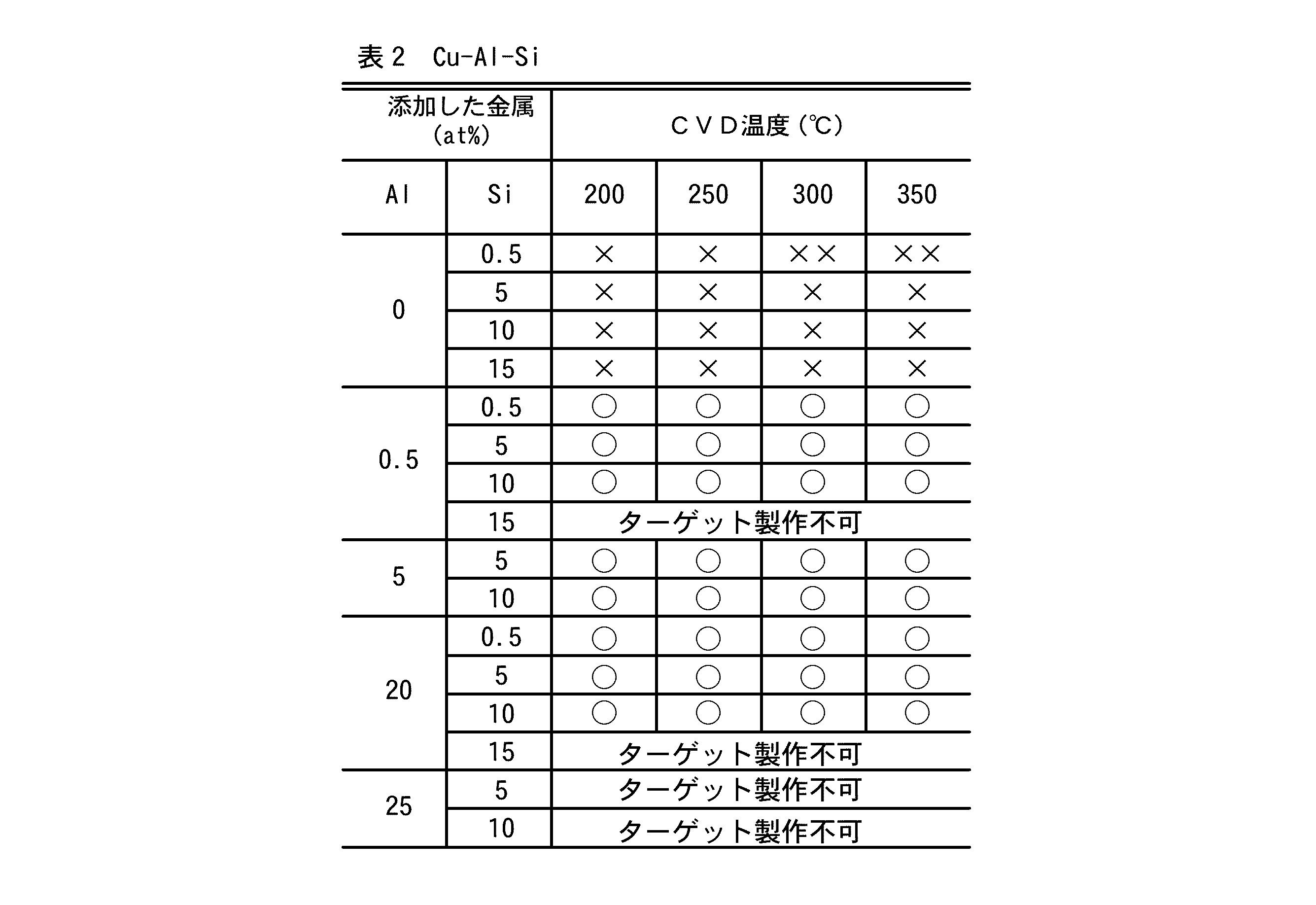
表2から、Alを0.5at%以上含有し、Siを0.5at%以上含有すれば、全て良品になるので好ましい。
なお、Alを25at%以上含有させた場合や、Siを15at%以上含有させた場合には、現状の技術ではCu合金ターゲットを作成することができない。そのため、Siは15at%未満の範囲で含有させればよいが、15at%以上でもCu合金ターゲットを形成できる可能性があるので15at%未満の範囲に限定されるものではない。
<Cu-Al-Ni>
Cap膜用合金の原子数を100at%としたときに、Alを0at%以上25at%以下の範囲で含有させ、添加金属として、金属材料であるNiを3at%以上50at%以下の範囲で含有させたCap膜用合金を作成してCu合金ターゲットを製造し、スパッタリングによって本体膜上にCap膜を形成し、200℃以上350℃以下の温度範囲のCVD法によってCap膜上に絶縁膜を形成し、剥離試験を行った。
Cap膜用合金の原子数を100at%としたときに、Alを0at%以上25at%以下の範囲で含有させ、添加金属として、金属材料であるNiを3at%以上50at%以下の範囲で含有させたCap膜用合金を作成してCu合金ターゲットを製造し、スパッタリングによって本体膜上にCap膜を形成し、200℃以上350℃以下の温度範囲のCVD法によってCap膜上に絶縁膜を形成し、剥離試験を行った。
Al含有率及びNi含有率とCVDの温度とから成る成膜条件と、各成膜条件に対応した剥離試験結果とを下記表3に記載する。
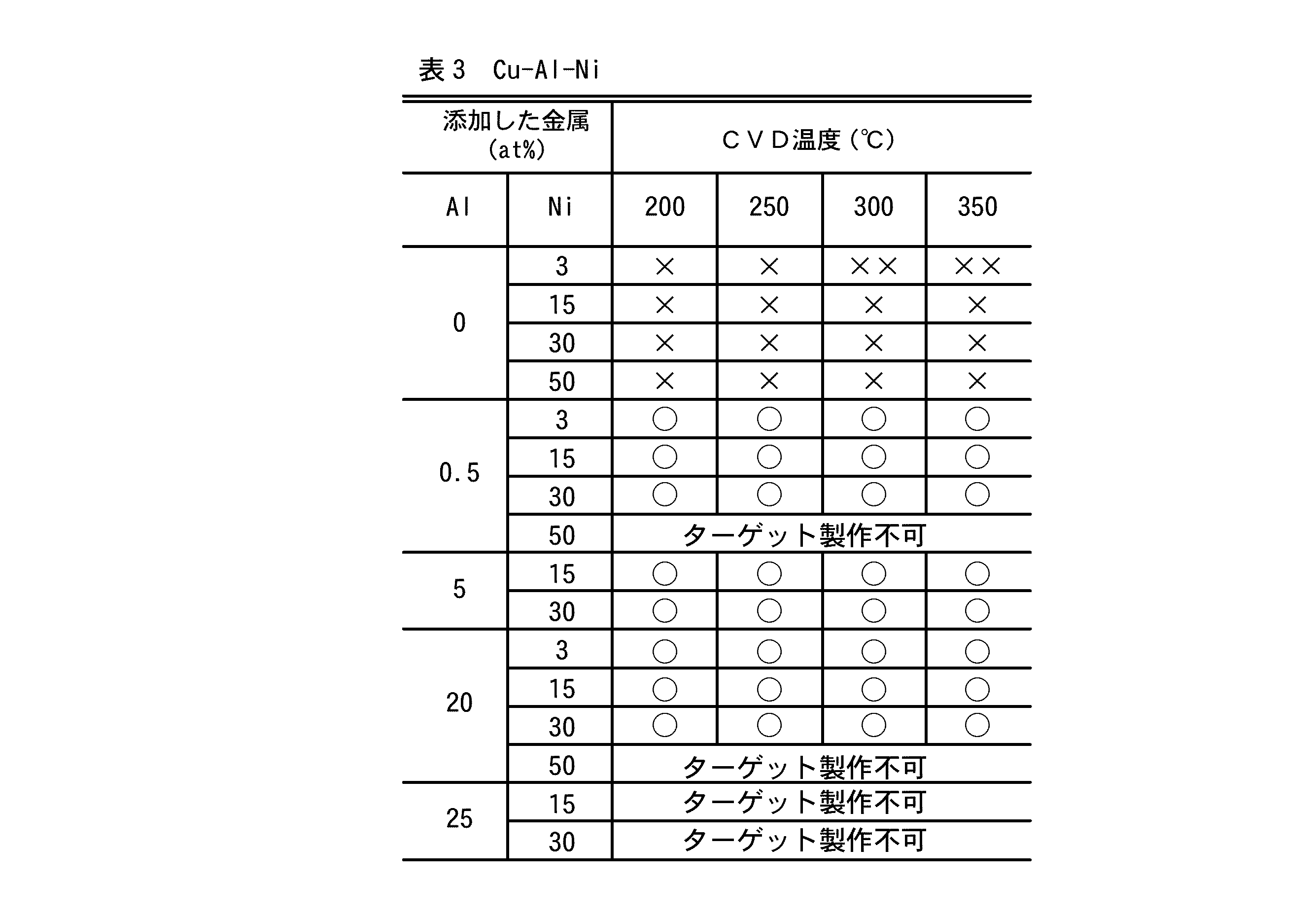
表3から、Alを0.5at%以上含有し、Niを3at%以上含有すれば、全て良品になるので好ましい。
なお、 Alを25at%以上含有させた場合や、Niを50at%以上含有させた場合には、現状の技術ではCu合金ターゲットを作成することができない。そのため、Niは50at%未満の範囲で含有させればよい。
<Cu-Ca>
Cap膜用合金の原子数を100at%としたときに、添加金属として、金属材料であるCaを0at%以上10at%以下の範囲で含有させたCap膜用合金を作成してCu合金ターゲットを製造し、スパッタリングによって本体膜上にCap膜を形成し、200℃以上350℃以下の温度範囲のCVD法によってCap膜上に絶縁膜を形成し、剥離試験を行った。
Cap膜用合金の原子数を100at%としたときに、添加金属として、金属材料であるCaを0at%以上10at%以下の範囲で含有させたCap膜用合金を作成してCu合金ターゲットを製造し、スパッタリングによって本体膜上にCap膜を形成し、200℃以上350℃以下の温度範囲のCVD法によってCap膜上に絶縁膜を形成し、剥離試験を行った。
Cu含有率とCVDの温度とから成る成膜条件と、各成膜条件に対応した剥離試験結果とを下記表4に記載する。

表4から、Caを0.5at%以上含有すれば、全て良品になるので好ましい。
なお、 Caを7at%以上含有させると、現状の技術ではCu合金ターゲットを作成することができない。そのため、Caは7at%未満の範囲で含有させればよいが、7at%以上含有させてもCu合金ターゲットが形成できる可能性があるので7at%未満の範囲に限定されるものではない。
<Cu-Al>
比較例として、Cap膜用合金の原子数を100at%としたときに、Alを0at%以上25at%以下の範囲で含有させたCap膜用合金を作成してCu合金ターゲットを製造し、スパッタリングによって本体膜上にCap膜を形成し、200℃以上350℃以下の温度範囲のCVD法によってCap膜上に絶縁膜を形成し、剥離試験を行った。
比較例として、Cap膜用合金の原子数を100at%としたときに、Alを0at%以上25at%以下の範囲で含有させたCap膜用合金を作成してCu合金ターゲットを製造し、スパッタリングによって本体膜上にCap膜を形成し、200℃以上350℃以下の温度範囲のCVD法によってCap膜上に絶縁膜を形成し、剥離試験を行った。
Al含有率とCVDの温度とから成る成膜条件と、各成膜条件に対応した剥離試験結果とを下記表5に記載する。
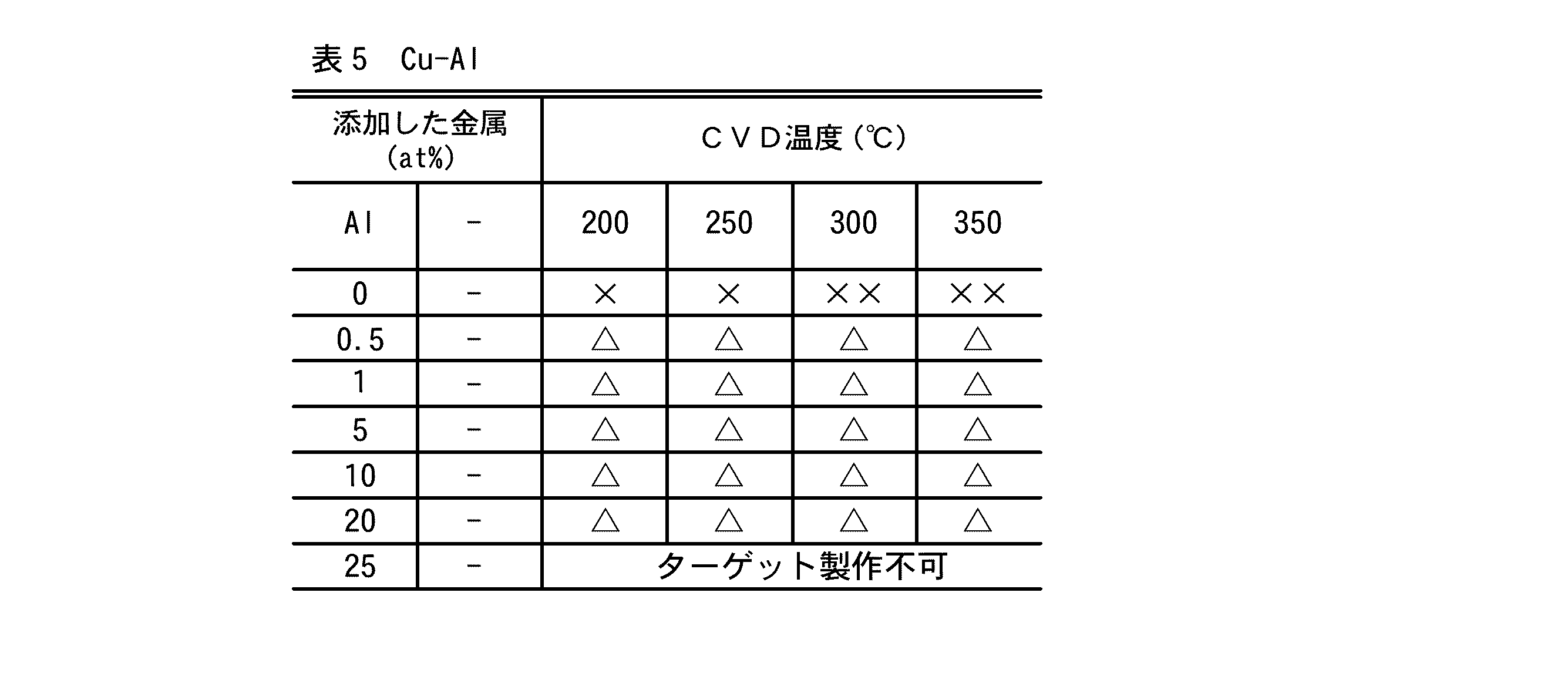
Alを0.5at%以上含有させると、使用不可品や不良品は発生せず、実使用に耐えられる配線膜と絶縁膜とが得られるが、並品ばかりであり、良品は得られていない。従って、Alだけを添加したときには好ましい範囲を得ることができないことが分かる。
なお、Alを25at%以上添加すると、現状の技術ではCu合金ターゲットを作成することができない。
<結論>
以上により、Cap膜用合金から成るCu合金ターゲットは、Cap膜用合金の原子数を100at%としたときに、50at%を超えるCuと、添加金属と、0.5at%以上のAlとを含有し、添加金属は、0.5at%以上のMgと、0.5at%以上のSiと、3at%以上のNiと、から成る三種の金属材料のうち、少なくとも一種以上の金属材料を含有すればよい。
以上により、Cap膜用合金から成るCu合金ターゲットは、Cap膜用合金の原子数を100at%としたときに、50at%を超えるCuと、添加金属と、0.5at%以上のAlとを含有し、添加金属は、0.5at%以上のMgと、0.5at%以上のSiと、3at%以上のNiと、から成る三種の金属材料のうち、少なくとも一種以上の金属材料を含有すればよい。
また、Cap膜用合金から成るCu合金ターゲットは、Cap膜用合金の原子数を100at%としたときに、Cap膜用合金は、50at%を超えるCuと、0.5at%以上のCaとを含有してもよい。
Cu合金ターゲットをスパッタリングして得られたCap膜の組成は、Cu合金ターゲットの組成と同じであり、半導体素子では、上記組成の配線膜はゲート電極膜、ソース電極膜、又はドレイン電極膜や、それらの電極膜同士を接続する配線膜に用いることができる。
なお、本発明とは別の発明について、上記説明と実施例の記載とから、1番目にCap膜用合金から成るCap膜と、前記Cap膜よりも抵抗率が小さい本体膜と、を有し、前記Cap膜と前記本体膜との積層構造にされた配線膜であって、前記Cap膜用合金の原子数を100at%としたときに、前記Cap膜用合金は、50at%を超えるCuと、添加金属と、0.5at%以上のAlとを含有し、前記添加金属は、0.5at%以上のMgと、0.5at%以上のSiと、3at%以上のNiと、から成る三種の金属材料のうち、少なくとも一種以上の金属材料を含有し、前記Cap膜はSi酸化物を含有する絶縁膜と接触された配線膜の発明を得ることができる。
また、二番目にCap膜用合金から成るCap膜と、前記Cap膜よりも抵抗率が小さい本体膜と、を有し、前記Cap膜と前記本体膜との積層構造にされた配線膜であって、前記Cap膜用合金の原子数を100at%としたときに、前記Cap膜用合金は、50at%を超えるCuと、0.5at%以上のCaとを含有する配線膜の発明を得ることができる。
また、3番目に、半導体層と、前記半導体層と接触して配置されたゲート絶縁膜と、前記ゲート絶縁膜を間にして前記半導体層と対向するゲート電極膜とを有し、前記半導体層には、前記ゲート電極膜と対向する部分にチャネル領域が設けられ、前記チャネル領域の両側にソース領域とドレイン領域とが設けられ、前記ソース領域と前記ドレイン領域には、ソース電極膜とドレイン電極膜がそれぞれ接触された半導体装置であって、前記ゲート電極膜は、Cap膜用合金から成るCap膜と、前記Cap膜よりも抵抗率が小さい本体膜とを有し、前記Cap膜と前記本体膜との積層構造にされ、前記Cap膜用合金の原子数を100at%としたときに、前記Cap膜用合金は、50at%を超えるCuと、添加金属と、0.5at%以上のAlとを含有し、前記添加金属には、0.5at%以上のMgと、0.5at%以上のSiと、3at%以上のNiと、から成る三種の金属材料のうち、少なくとも一種以上の金属材料が含有され、前記ゲート絶縁膜はSi酸化物を含有し、前記ゲート絶縁膜には前記Cap膜が接触された半導体装置の発明を得ることができる。
また、4番目に、半導体層と、前記半導体層と接触して配置されたゲート絶縁膜と、前記ゲート絶縁膜を間にして前記半導体層と対向するゲート電極膜とを有し、前記半導体層には、前記ゲート電極膜と対向する部分にチャネル領域が設けられ、前記チャネル領域の両側にソース領域とドレイン領域とが設けられ、前記ソース領域と前記ドレイン領域には、ソース電極膜とドレイン電極膜がそれぞれ接触された半導体装置であって、前記ゲート電極膜は、Cap膜用合金から成るCap膜と、前記Cap膜よりも抵抗率が小さい本体膜とを有し、前記Cap膜と前記本体膜との積層構造にされ、前記Cap膜用合金の原子数を100at%としたときに、前記Cap膜用合金は、50at%を超えるCuと、0.5at%以上のCaとを含有し、前記ゲート絶縁膜はSi酸化物を含有し、前記ゲート絶縁膜には前記Cap膜が接触された半導体装置の発明を得ることができる。
また、5番目に、半導体層と、前記半導体層と接触して配置されたゲート絶縁膜と、前記ゲート絶縁膜を間にして前記半導体層と対向するゲート電極膜とを有し、前記半導体層には、前記ゲート電極膜と対向する部分にチャネル領域が設けられ、前記チャネル領域の両側にソース領域とドレイン領域とが設けられ、前記ソース領域と前記ドレイン領域には、ソース電極膜の片面とドレイン電極膜の片面がそれぞれ接触され、前記ソース電極膜の反対面と前記ドレイン電極膜の反対面とは絶縁膜に接触した半導体装置であって、前記ソース電極膜と前記ドレイン電極膜のいずれか一方又は両方の電極膜はCap膜用合金から成るCap膜と、前記Cap膜よりも抵抗率が小さい本体膜とを有し、前記Cap膜と前記本体膜との積層構造にされ、前記Cap膜用合金の原子数を100at%としたときに、前記Cap膜用合金は、50at%を超えるCuと、添加金属と、0.5at%以上のAlとを含有し、前記添加金属には、0.5at%以上のMgと、0.5at%以上のSiと、3at%以上のNiと、から成る三種の金属材料のうち、少なくとも一種以上の金属材料が含有され、前記絶縁膜はSi酸化物を含有し、前記Cap膜が前記絶縁膜に接触された半導体装置の発明を得ることができる。
また、6番目に、半導体層と、前記半導体層と接触して配置されたゲート絶縁膜と、前記ゲート絶縁膜を間にして前記半導体層と対向するゲート電極膜とを有し、前記半導体層には、前記ゲート電極膜と対向する部分にチャネル領域が設けられ、前記チャネル領域の両側にソース領域とドレイン領域とが設けられ、前記ソース領域と前記ドレイン領域には、ソース電極膜の片面とドレイン電極膜の片面がそれぞれ接触され、前記ソース電極膜の反対面と前記ドレイン電極膜の反対面とは絶縁膜に接触した半導体装置であって、前記ソース電極膜と前記ドレイン電極膜のいずれか一方又は両方の電極膜はCap膜用合金から成るCap膜と、前記Cap膜よりも抵抗率が小さい本体膜とを有し、前記Cap膜と前記本体膜との積層構造にされ、前記Cap膜用合金の原子数を100at%としたときに、前記Cap膜用合金は、50at%を超えるCuと、0.5at%以上のCaとを含有し、前記絶縁膜はSi酸化物を含有し、前記Cap膜が前記絶縁膜に接触された半導体装置の発明を得ることができる。
また、7番目に、基板と、前記基板表面に設けられた配線膜と、前記基板上に配置された画素電極層と、前記画素電極層上に配置された液晶と、前記液晶上に配置された上部電極層と、を有し、前記画素電極層は、前記配線膜に電気的に接続された液晶表示装置であって、前記配線膜は、Cap膜用合金から成るCap膜と、前記Cap膜よりも抵抗率が小さい本体膜とを有し、前記Cap膜用合金の原子数を100at%としたときに、前記Cap膜用合金は、50at%を超えるCuと、添加金属と、0.5at%以上のAlとを含有し、前記添加金属は、0.5at%以上のMgと、0.5at%以上のSiと、3at%以上のNiと、から成る三種の金属材料のうち、少なくとも一種以上の金属材料を含有し、前記Cap膜はSi酸化物を含有する絶縁膜に接触された液晶表示装置の発明を得ることができる。
また、8番目に、基板と、前記基板表面に設けられた配線膜と、前記基板上に配置された画素電極層と、前記画素電極層上に配置された液晶と、前記液晶上に配置された上部電極層と、を有し、前記画素電極層は、前記配線膜に電気的に接続された液晶表示装置であって、前記配線膜は、Cap膜用合金から成るCap膜と、前記Cap膜よりも抵抗率が小さい本体膜とを有し、前記Cap膜用合金の原子数を100at%としたときに、前記Cap膜用合金は、50at%を超えるCuと、0.5at%以上のCaとを含有し、前記Cap膜はSi酸化物を含有する絶縁膜に接触された液晶表示装置の発明を得ることができる。
以上説明した1、3、5、7番目の発明では、前記添加金属が、0.5at%以上7%未満のMgである発明を得ることができる。
また、1、3、5、7番目の発明では、前記添加金属が、0.5at%以上15%未満のSiである発明を得ることができる。
また、1、3、5、7番目の発明では、前記添加金属が、0.5at%以上15%未満のSiである発明を得ることができる。
1、3、5、7番目の発明では、前記添加金属が、3at%以上50%未満のNiである発明を得ることができる。
Cap膜上には、CVD法によってSi酸化物薄膜がCap膜に密着して形成される。
Cap膜上には、CVD法によってSi酸化物薄膜がCap膜に密着して形成される。
11……TFT
35……配線膜
31……基板
32……ゲート電極膜
33……ゲート絶縁膜
34……半導体層
36……密着層
37……低抵抗層
41……保護絶縁膜
43……接続孔
51……ソース電極膜
52……ドレイン電極膜
71……ソース領域
72……ドレイン領域
73……チャネル領域
81……上部電極
82……画素電極
83……液晶
88c……Cu合金ターゲット
35……配線膜
31……基板
32……ゲート電極膜
33……ゲート絶縁膜
34……半導体層
36……密着層
37……低抵抗層
41……保護絶縁膜
43……接続孔
51……ソース電極膜
52……ドレイン電極膜
71……ソース領域
72……ドレイン領域
73……チャネル領域
81……上部電極
82……画素電極
83……液晶
88c……Cu合金ターゲット
Claims (5)
- Cap膜用合金から成るCu合金ターゲットであって、
前記Cap膜用合金の原子数を100at%としたときに、前記Cap膜用合金は、50at%を超えるCuと、添加金属と、0.5at%以上のAlとを含有し、
前記添加金属は、0.5at%以上のMgと、0.5at%以上のSiと、3at%以上のNiと、から成る三種の金属材料のうち、少なくとも一種以上の金属材料を含有するCu合金ターゲット。 - 前記添加金属は、0.5at%以上7at%未満のMgである請求項1記載のCu合金ターゲット。
- 前記添加金属は、0.5at%以上15at%未満のSiである請求項1記載のCu合金ターゲット。
- 前記添加金属は、3at%以上50at%未満のNiである請求項1記載のCu合金ターゲット。
- Cap膜用合金から成るCu合金ターゲットであって、
前記Cap膜用合金の原子数を100at%としたときに、前記Cap膜用合金は、50at%を超えるCuと、0.5at%以上のCaとを含有するCu合金ターゲット。
Priority Applications (3)
| Application Number | Priority Date | Filing Date | Title |
|---|---|---|---|
| US16/965,185 US20210230718A1 (en) | 2019-04-19 | 2020-02-06 | Cu ALLOY TARGET |
| KR1020207016854A KR20200123082A (ko) | 2019-04-19 | 2020-02-06 | Cu 합금 타깃 |
| JP2020529771A JPWO2020213232A1 (ja) | 2019-04-19 | 2020-02-06 | Cu合金ターゲット |
Applications Claiming Priority (2)
| Application Number | Priority Date | Filing Date | Title |
|---|---|---|---|
| JP2019080031 | 2019-04-19 | ||
| JP2019-080031 | 2019-04-19 |
Publications (1)
| Publication Number | Publication Date |
|---|---|
| WO2020213232A1 true WO2020213232A1 (ja) | 2020-10-22 |
Family
ID=72838185
Family Applications (1)
| Application Number | Title | Priority Date | Filing Date |
|---|---|---|---|
| PCT/JP2020/004644 Ceased WO2020213232A1 (ja) | 2019-04-19 | 2020-02-06 | Cu合金ターゲット |
Country Status (5)
| Country | Link |
|---|---|
| US (1) | US20210230718A1 (ja) |
| JP (1) | JPWO2020213232A1 (ja) |
| KR (1) | KR20200123082A (ja) |
| TW (1) | TW202041688A (ja) |
| WO (1) | WO2020213232A1 (ja) |
Citations (3)
| Publication number | Priority date | Publication date | Assignee | Title |
|---|---|---|---|---|
| JP2011049543A (ja) * | 2009-07-27 | 2011-03-10 | Kobe Steel Ltd | 配線構造およびその製造方法、並びに配線構造を備えた表示装置 |
| WO2011162177A1 (ja) * | 2010-06-21 | 2011-12-29 | 株式会社アルバック | 半導体装置、半導体装置を有する液晶表示装置、半導体装置の製造方法 |
| JP2017208533A (ja) * | 2016-05-13 | 2017-11-24 | 株式会社神戸製鋼所 | 積層配線膜および薄膜トランジスタ素子 |
Family Cites Families (2)
| Publication number | Priority date | Publication date | Assignee | Title |
|---|---|---|---|---|
| JPH06177117A (ja) * | 1992-12-07 | 1994-06-24 | Japan Energy Corp | スパッタターゲットとこれを使用する半導体装置の製造方法 |
| WO2018189965A1 (ja) * | 2017-04-13 | 2018-10-18 | 株式会社アルバック | 液晶表示装置、有機el表示装置、半導体素子、配線膜、配線基板、ターゲット |
-
2020
- 2020-02-06 JP JP2020529771A patent/JPWO2020213232A1/ja active Pending
- 2020-02-06 KR KR1020207016854A patent/KR20200123082A/ko not_active Ceased
- 2020-02-06 WO PCT/JP2020/004644 patent/WO2020213232A1/ja not_active Ceased
- 2020-02-06 US US16/965,185 patent/US20210230718A1/en not_active Abandoned
- 2020-02-27 TW TW109106377A patent/TW202041688A/zh unknown
Patent Citations (3)
| Publication number | Priority date | Publication date | Assignee | Title |
|---|---|---|---|---|
| JP2011049543A (ja) * | 2009-07-27 | 2011-03-10 | Kobe Steel Ltd | 配線構造およびその製造方法、並びに配線構造を備えた表示装置 |
| WO2011162177A1 (ja) * | 2010-06-21 | 2011-12-29 | 株式会社アルバック | 半導体装置、半導体装置を有する液晶表示装置、半導体装置の製造方法 |
| JP2017208533A (ja) * | 2016-05-13 | 2017-11-24 | 株式会社神戸製鋼所 | 積層配線膜および薄膜トランジスタ素子 |
Also Published As
| Publication number | Publication date |
|---|---|
| JPWO2020213232A1 (ja) | 2021-05-06 |
| US20210230718A1 (en) | 2021-07-29 |
| TW202041688A (zh) | 2020-11-16 |
| KR20200123082A (ko) | 2020-10-28 |
Similar Documents
| Publication | Publication Date | Title |
|---|---|---|
| JP5017282B2 (ja) | 配線膜の形成方法 | |
| JP4970622B2 (ja) | 半導体装置、半導体装置を有する液晶表示装置、半導体装置の製造方法 | |
| KR101175970B1 (ko) | 배선층, 반도체 장치, 액정 표시 장치 | |
| JP5963804B2 (ja) | 半導体装置の製造方法 | |
| US20070228575A1 (en) | Wiring material and wiring board using the same | |
| WO2012132871A1 (ja) | Cu合金膜、及びそれを備えた表示装置または電子装置 | |
| JPWO2008081805A1 (ja) | 配線膜の形成方法、トランジスタ、及び電子装置 | |
| JP4913267B2 (ja) | 配線層、半導体装置、半導体装置を有する液晶表示装置 | |
| JP2008124450A (ja) | ターゲット、成膜方法、薄膜トランジスタ、薄膜トランジスタ付パネル、薄膜トランジスタの製造方法、及び薄膜トランジスタ付パネルの製造方法 | |
| JP2009280834A (ja) | ターゲット、配線膜形成方法、薄膜トランジスタの製造方法 | |
| WO2008047511A1 (en) | Al-Ni-B ALLOY MATERIAL FOR REFLECTION FILM | |
| JP6768180B1 (ja) | Cu合金ターゲット、配線膜、半導体装置、液晶表示装置 | |
| JPWO2020213232A1 (ja) | Cu合金ターゲット | |
| JP7339016B2 (ja) | 表示装置、配線膜、配線膜製造方法 | |
| JP2006330662A (ja) | 表示デバイスの素子構造 | |
| JP2008306043A (ja) | 配線膜の形成方法、トランジスタ、及び電子装置 | |
| JP2020012190A (ja) | 密着膜用ターゲット、配線層、半導体装置、液晶表示装置 |
Legal Events
| Date | Code | Title | Description |
|---|---|---|---|
| ENP | Entry into the national phase |
Ref document number: 2020529771 Country of ref document: JP Kind code of ref document: A |
|
| 121 | Ep: the epo has been informed by wipo that ep was designated in this application |
Ref document number: 20791208 Country of ref document: EP Kind code of ref document: A1 |
|
| NENP | Non-entry into the national phase |
Ref country code: DE |
|
| 122 | Ep: pct application non-entry in european phase |
Ref document number: 20791208 Country of ref document: EP Kind code of ref document: A1 |