WO2020209043A1 - 電子部品用テープおよび電子部品の加工方法 - Google Patents
電子部品用テープおよび電子部品の加工方法 Download PDFInfo
- Publication number
- WO2020209043A1 WO2020209043A1 PCT/JP2020/012847 JP2020012847W WO2020209043A1 WO 2020209043 A1 WO2020209043 A1 WO 2020209043A1 JP 2020012847 W JP2020012847 W JP 2020012847W WO 2020209043 A1 WO2020209043 A1 WO 2020209043A1
- Authority
- WO
- WIPO (PCT)
- Prior art keywords
- tape
- resin layer
- thickness
- semiconductor wafer
- electronic components
- Prior art date
- Legal status (The legal status is an assumption and is not a legal conclusion. Google has not performed a legal analysis and makes no representation as to the accuracy of the status listed.)
- Ceased
Links
Images

Classifications
-
- C—CHEMISTRY; METALLURGY
- C09—DYES; PAINTS; POLISHES; NATURAL RESINS; ADHESIVES; COMPOSITIONS NOT OTHERWISE PROVIDED FOR; APPLICATIONS OF MATERIALS NOT OTHERWISE PROVIDED FOR
- C09J—ADHESIVES; NON-MECHANICAL ASPECTS OF ADHESIVE PROCESSES IN GENERAL; ADHESIVE PROCESSES NOT PROVIDED FOR ELSEWHERE; USE OF MATERIALS AS ADHESIVES
- C09J7/00—Adhesives in the form of films or foils
- C09J7/20—Adhesives in the form of films or foils characterised by their carriers
- C09J7/22—Plastics; Metallised plastics
- C09J7/25—Plastics; Metallised plastics based on macromolecular compounds obtained otherwise than by reactions involving only carbon-to-carbon unsaturated bonds
- C09J7/255—Polyesters
-
- C—CHEMISTRY; METALLURGY
- C09—DYES; PAINTS; POLISHES; NATURAL RESINS; ADHESIVES; COMPOSITIONS NOT OTHERWISE PROVIDED FOR; APPLICATIONS OF MATERIALS NOT OTHERWISE PROVIDED FOR
- C09J—ADHESIVES; NON-MECHANICAL ASPECTS OF ADHESIVE PROCESSES IN GENERAL; ADHESIVE PROCESSES NOT PROVIDED FOR ELSEWHERE; USE OF MATERIALS AS ADHESIVES
- C09J201/00—Adhesives based on unspecified macromolecular compounds
-
- C—CHEMISTRY; METALLURGY
- C09—DYES; PAINTS; POLISHES; NATURAL RESINS; ADHESIVES; COMPOSITIONS NOT OTHERWISE PROVIDED FOR; APPLICATIONS OF MATERIALS NOT OTHERWISE PROVIDED FOR
- C09J—ADHESIVES; NON-MECHANICAL ASPECTS OF ADHESIVE PROCESSES IN GENERAL; ADHESIVE PROCESSES NOT PROVIDED FOR ELSEWHERE; USE OF MATERIALS AS ADHESIVES
- C09J7/00—Adhesives in the form of films or foils
- C09J7/20—Adhesives in the form of films or foils characterised by their carriers
- C09J7/22—Plastics; Metallised plastics
- C09J7/24—Plastics; Metallised plastics based on macromolecular compounds obtained by reactions involving only carbon-to-carbon unsaturated bonds
-
- C—CHEMISTRY; METALLURGY
- C09—DYES; PAINTS; POLISHES; NATURAL RESINS; ADHESIVES; COMPOSITIONS NOT OTHERWISE PROVIDED FOR; APPLICATIONS OF MATERIALS NOT OTHERWISE PROVIDED FOR
- C09J—ADHESIVES; NON-MECHANICAL ASPECTS OF ADHESIVE PROCESSES IN GENERAL; ADHESIVE PROCESSES NOT PROVIDED FOR ELSEWHERE; USE OF MATERIALS AS ADHESIVES
- C09J7/00—Adhesives in the form of films or foils
- C09J7/20—Adhesives in the form of films or foils characterised by their carriers
- C09J7/22—Plastics; Metallised plastics
- C09J7/25—Plastics; Metallised plastics based on macromolecular compounds obtained otherwise than by reactions involving only carbon-to-carbon unsaturated bonds
-
- C—CHEMISTRY; METALLURGY
- C09—DYES; PAINTS; POLISHES; NATURAL RESINS; ADHESIVES; COMPOSITIONS NOT OTHERWISE PROVIDED FOR; APPLICATIONS OF MATERIALS NOT OTHERWISE PROVIDED FOR
- C09J—ADHESIVES; NON-MECHANICAL ASPECTS OF ADHESIVE PROCESSES IN GENERAL; ADHESIVE PROCESSES NOT PROVIDED FOR ELSEWHERE; USE OF MATERIALS AS ADHESIVES
- C09J7/00—Adhesives in the form of films or foils
- C09J7/30—Adhesives in the form of films or foils characterised by the adhesive composition
- C09J7/35—Heat-activated
-
- H—ELECTRICITY
- H10—SEMICONDUCTOR DEVICES; ELECTRIC SOLID-STATE DEVICES NOT OTHERWISE PROVIDED FOR
- H10P—GENERIC PROCESSES OR APPARATUS FOR THE MANUFACTURE OR TREATMENT OF DEVICES COVERED BY CLASS H10
- H10P52/00—Grinding, lapping or polishing of wafers, substrates or parts of devices
-
- H—ELECTRICITY
- H10—SEMICONDUCTOR DEVICES; ELECTRIC SOLID-STATE DEVICES NOT OTHERWISE PROVIDED FOR
- H10P—GENERIC PROCESSES OR APPARATUS FOR THE MANUFACTURE OR TREATMENT OF DEVICES COVERED BY CLASS H10
- H10P72/00—Handling or holding of wafers, substrates or devices during manufacture or treatment thereof
- H10P72/70—Handling or holding of wafers, substrates or devices during manufacture or treatment thereof for supporting or gripping
-
- C—CHEMISTRY; METALLURGY
- C09—DYES; PAINTS; POLISHES; NATURAL RESINS; ADHESIVES; COMPOSITIONS NOT OTHERWISE PROVIDED FOR; APPLICATIONS OF MATERIALS NOT OTHERWISE PROVIDED FOR
- C09J—ADHESIVES; NON-MECHANICAL ASPECTS OF ADHESIVE PROCESSES IN GENERAL; ADHESIVE PROCESSES NOT PROVIDED FOR ELSEWHERE; USE OF MATERIALS AS ADHESIVES
- C09J2203/00—Applications of adhesives in processes or use of adhesives in the form of films or foils
- C09J2203/326—Applications of adhesives in processes or use of adhesives in the form of films or foils for bonding electronic components such as wafers, chips or semiconductors
-
- C—CHEMISTRY; METALLURGY
- C09—DYES; PAINTS; POLISHES; NATURAL RESINS; ADHESIVES; COMPOSITIONS NOT OTHERWISE PROVIDED FOR; APPLICATIONS OF MATERIALS NOT OTHERWISE PROVIDED FOR
- C09J—ADHESIVES; NON-MECHANICAL ASPECTS OF ADHESIVE PROCESSES IN GENERAL; ADHESIVE PROCESSES NOT PROVIDED FOR ELSEWHERE; USE OF MATERIALS AS ADHESIVES
- C09J2301/00—Additional features of adhesives in the form of films or foils
- C09J2301/30—Additional features of adhesives in the form of films or foils characterized by the chemical, physicochemical or physical properties of the adhesive or the carrier
- C09J2301/312—Additional features of adhesives in the form of films or foils characterized by the chemical, physicochemical or physical properties of the adhesive or the carrier parameters being the characterizing feature
Definitions
- the present invention relates to a tape for electronic parts and a processing method for electronic parts. More specifically, the present invention relates to a tape for electronic parts that can be mainly applied to a thin film grinding process of a semiconductor wafer, and a method for processing an electronic part using the tape for electronic parts.
- the back surface of the semiconductor wafer is usually subjected to backside grinding, etching, or the like in order to reduce the thickness of the semiconductor wafer after pattern formation.
- a semiconductor wafer surface protection tape is attached to the pattern surface for the purpose of protecting the pattern on the semiconductor wafer surface.
- the semiconductor wafer surface protection tape is generally used by laminating an adhesive layer on a base film and attaching an adhesive layer to the back surface of the semiconductor wafer (see, for example, Patent Document 1). ).
- the semiconductor wafer surface protection tape cannot be sufficiently adhered to and held on the wafer surface due to the high bumps. Then, cutting water and silicon grinding debris injected during grinding infiltrate through the gap between the semiconductor wafer surface protection tape and the wafer, and a phenomenon called sea page that contaminates the wafer surface occurs.
- an intermediate layer having a storage elastic modulus of 1 ⁇ 10 4 to 1 ⁇ 10 6 Pa is provided between the base film and the pressure-sensitive adhesive layer.
- the provided semiconductor wafer surface protection tape has been proposed (see, for example, Patent Document 2). Further, a semiconductor wafer surface protection tape in which a thermoplastic resin intermediate layer having a JIS-A hardness of 10 to 55 and a thickness of 25 to 400 ⁇ m is provided between the base film and the pressure-sensitive adhesive layer has also been proposed (for example). , Patent Documents 3 and 4).
- Japanese Unexamined Patent Publication No. 2000-8010 Japanese Unexamined Patent Publication No. 2014-17336 Japanese Patent No. 4054113 Japanese Patent No. 37733558
- the semiconductor wafer surface protection tape described in the above-mentioned patent document when the semiconductor wafer surface protection tape is intended to follow the unevenness of the semiconductor wafer surface, the semiconductor wafer surface protection tape is attached to the semiconductor wafer. At that time, since it is necessary to heat the semiconductor wafer surface protection tape to make it flexible, there is a problem that it takes time for bonding.
- an object of the present invention is to provide a tape for electronic parts and a processing method for electronic parts, which can sufficiently follow a semiconductor wafer having bumps having a large height in a short time.
- the tape for electronic components according to the present invention has at least one resin layer, and the resin layer is measured at 60 ° C. to 80 ° C. using a nanoindenter according to ISO14577.
- the feature is that the indenter indentation depth of the nanoindenter at any temperature is 10,000 nm to 50,000 nm, the thickness of the resin layer is 50 ⁇ m to 300 ⁇ m, and the total thickness is 450 ⁇ m or less.
- the resin layer has a thermal conductivity of at least 0.30 W / m ⁇ K or more at 60 to 80 ° C.
- the tape for electronic components is preferably attached to the circuit forming surface of a semiconductor wafer provided with a step of 10 ⁇ m or more.
- the thickness of the resin layer of the tape for electronic components is preferably 1 time or more and 2 times or less of the step.
- the method for processing an electronic component according to the present invention is to apply the above-mentioned tape for electronic components to a temperature of 50 to 100 ° C. on a circuit forming surface of a semiconductor wafer provided with a step of 10 ⁇ m or more. It is characterized by having a bonding step of bonding with the above, and a grinding step of grinding a surface of the semiconductor wafer opposite to the circuit forming surface after the bonding step.
- the bonding speed in the bonding step is 3 mm / S or more.
- the tape for electronic components it is possible to sufficiently follow a semiconductor wafer having bumps having a large height in a short time.
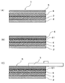
- FIG. 1 is a cross-sectional view schematically showing the structure of the tape 1 for electronic components according to the embodiment of the present invention.
- the tape 1 for electronic components has a base film 2, and a resin layer 3 is provided on at least one side of the base film 2.
- the pressure-sensitive adhesive layer 4 is provided on the upper surface of the resin layer 3, and the release-treated surface of the release film 5 whose surface has been released-treated is in contact with the pressure-sensitive adhesive layer 4 on the upper surface of the pressure-sensitive adhesive layer 4. It is laminated on.
- a release film is provided in the present embodiment, the release film 5 does not necessarily have to be provided.
- Base film 2 Known plastics, rubbers, etc. can be used as the base film 2 of the tape 1 for electronic components of the present invention.
- the base film 2 in particular, when a radiation-curable composition is used for the pressure-sensitive adhesive layer 4, it is preferable to select a base film 2 having good radiation transmission at a wavelength at which the composition is cured.
- radiation is a general term for, for example, light such as ultraviolet rays, laser light, or ionizing radiation such as an electron beam, and hereinafter, these are collectively referred to as radiation.
- Examples of resins that can be selected as such a base film 2 include high-density polyethylene (HDPE), low-density polyethylene (LDPE), polypropylene (PP), ethylene-vinyl acetate copolymer (EVA), and ethylene acrylic acid.
- Polyethylenes such as copolymers and ethylene methacrylate copolymers and their metal crosslinks (ionomers), polyesters such as polyethylene terephthalate (PET), polyethylene terephthalate (PEN), and polyethylene terephthalate (PBT), Further, a film formed by cross-linking an acrylic resin can be used.
- Each resin may be used alone as a single-layer base material, may be mixed by combining resins, or may have a multi-layer structure of different resins. Further, additives may be added as long as the physical properties are not affected, such as blending a coloring pigment or the like for recognizing and identifying the semiconductor wafer surface protective adhesive tape 1.
- the base film 2 preferably has a tensile elastic modulus of 0.01 to 10 GPa at 25 ° C., preferably 0.1 to 5 GPa, in order to handle the tape 1 for electronic components and suppress warpage during thin film grinding of the semiconductor wafer 6. More preferred. Further, when the base film 2 is the outermost surface, it is required to withstand the processing heat due to heat bonding of the electronic component tape 1 and polishing of the semiconductor wafer 6, and the back surface of the tape when the electronic component tape 1 is peeled off. When used in a step of heat-pressing and peeling a heat-sealing film, the melting point is preferably 70 to 170 ° C, more preferably 90 to 140 ° C.
- the thickness of the base film 2 is not particularly limited and may be set as appropriate, but is preferably 10 to 300 ⁇ m, more preferably 25 to 100 ⁇ m.
- the method for producing the base film 2 is not particularly limited. Conventional methods such as a calendar method, a T-die extrusion method, an inflation method, and the like can be used. In addition, an independently formed film and another film can be bonded together with an adhesive or the like to form a base film.
- the surface of the base film 2 on the side where the resin layer 3 is provided may be appropriately subjected to a treatment such as a corona treatment or a primer layer in order to improve the adhesion with the resin layer 3. It is also preferable that the surface of the base film 2 on the side where the resin layer 3 is not provided is textured or coated with a lubricant, whereby the effect of preventing blocking during storage of the tape 1 for electronic components of the present invention can be obtained. be able to.
- the surface of the base film 2 on the side where the resin layer 3 is not provided is provided with heat seal and adhesiveness. It is also preferable to provide a coating or a resin layer to have.
- the melting point of these heat seal layers is preferably 70 to 170 ° C, more preferably 90 to 140 ° C.
- the heat seal layer is effective.
- the nano indenter of the resin layer 3 As the resin constituting the resin layer 3, the nano indenter of the resin layer 3 is used, and the pressing depth of the indenter of the nano indenter at any temperature of 60 ° C. to 80 ° C. measured according to ISO14577 is 10,000 nm.
- a known resin can be used without particular limitation as long as it has a temperature of about 50,000 nm.
- resins that can be selected as the resin layer 3 include polyethylene, ethylene-vinyl acetate copolymer, ethylene-ethyl acrylate copolymer, ethylene-methyl acrylate copolymer, ethylene-acrylic acid copolymer, and ionomer. Examples thereof include homopolymers and copolymers of ⁇ -olefins such as. Each resin may be used alone as a single layer, these resins may be combined and mixed, or a multi-layer structure of different resins may be formed.
- the resin layer 3 has an indenter indentation depth of 10,000 nm to 50,000 nm at any temperature of 60 ° C. to 80 ° C. measured in accordance with ISO14577 using a nanoindenter. If the indenter pushing depth of the nanoindenter is less than 10000 nm at any temperature of 60 ° C to 80 ° C, it takes time for the tape 1 for electronic components to sufficiently follow the unevenness 61 on the surface of the semiconductor wafer 6. ..
- the indenter pushing depth of the nanoindenter exceeds 50,000 nm at any temperature of 60 ° C to 80 ° C, it will be deformed too much by heat bonding, and the thickness accuracy of the electronic component tape 1 will deteriorate. Since the resin layer 3 protrudes from the side surface of the semiconductor wafer 6, burrs and lumps are formed when the tape 1 for electronic components is cut along the side surface of the semiconductor wafer 6 to contaminate the semiconductor wafer 6. When burrs or the like are generated in the cut portion of the resin layer 3, when the back surface of the semiconductor wafer 6 is ground or polished, the burrs or the like are caught in the processed surface, and edge cracks or cracks are generated in the semiconductor wafer 6.
- the frictional heat generated by processing during polishing of the semiconductor wafer 6 such as dry polishing may exceed 60 ° C., which may cause damage to the semiconductor wafer 6 or poor thickness accuracy.
- the end portion of the electronic component tape 1 is softened, and the electronic component tape 1 is transported or stored in a scroll shape.
- misattachment at the edges and peripheral contamination due to softened resin are also possible.
- the indenter indentation depth of the nanoindenter conforms to ISO14577-1: 2002, and a load is applied to the Berkovich indenter made of diamond of the nanoindenter using the nanoindenter, and the indenter is applied to the sample surface at 10 mN. This is the indenter reaching depth when the depth at which the force is applied is set to zero and the sample is pushed in until a force of 50 mN is applied.
- the indentation depth of the nanoindenter indenter at 60 to 80 ° C. of the resin layer 3 can be adjusted by, for example, the density of the resin or the comonomer content ratio in the case of a comonomer copolymer.
- the comonomer content is preferably 10 to 50% by mass, more preferably 25 to 45%.
- the density is preferably 0.87 to 0.93, more preferably 0.88 to 0.90.
- the molecular weight of the resin can be adjusted, and the weight average molecular weight is preferably 10,000 to 200,000, more preferably 40,000 to 80,000.
- the thermal conductivity of the resin layer 3 at 60 to 80 ° C. is at least 0.30 W / m ⁇ K or more, and more preferably 0.4 W / m ⁇ K or more at 70 ° C. Thermal conductivity is measured according to JIS A1412. In order to make the thermal conductivity of the resin layer 3 at 60 to 80 ° C. to 0.30 W / m ⁇ K or more, a resin having such characteristics may be used, or a thermally conductive filler may be contained. ..
- the thermally conductive filler is preferably one or more selected from inorganic nitrides, inorganic oxides, and metals, and specific examples thereof include inorganic nitrides such as aluminum nitride and boron nitride. , Inorganic oxides such as alumina, silicon oxide and magnesium oxide, metals such as gold, silver, nickel and aluminum, and anti-blocking agents such as talc, calcium carbonate and silicon dioxide. Of these, aluminum nitride, which exhibits insulating properties and high thermal conductivity, is preferable. More preferably, surface-treated aluminum nitride is used for improving water resistance. These may be used alone or in admixture of two or more.
- the content ratio of the filler in the resin layer 3 is preferably 3 to 60% by mass, more preferably 20 to 50% by mass, based on the total mass of the resin layer 3.
- the resin layer 3 may contain a stabilizer, a lubricant, an antioxidant, a pigment, a plasticizer, or the like, if necessary. However, depending on the type and content of the additive, the pressure-sensitive adhesive layer and the semiconductor wafer may be contaminated. In that case, it is preferable to provide a barrier layer between the resin layer 3 and the pressure-sensitive adhesive layer.
- the thickness of the resin layer 3 is 50 to 300 ⁇ m, preferably 150 to 270 ⁇ m. If the thickness of the resin layer 3 is less than 50 ⁇ m, it becomes difficult for the tape 1 for electronic components to sufficiently follow the unevenness 61 on the surface of the semiconductor wafer 6. If the thickness of the resin layer 3 is more than 300 ⁇ m, the thermal conductivity is deteriorated and it takes time for the resin layer 3 to be flexible when the tape 1 for electronic components is heat-bonded to the surface of the semiconductor wafer 6. It takes time for the tape 1 for electronic components to sufficiently follow the unevenness 61 on the surface of the semiconductor wafer 6.
- the thickness of the resin layer 3 is preferably 1 time or more and 2 times or less the step on the surface of the semiconductor wafer 6. If the thickness of the resin layer 3 is less than one times the step on the surface of the semiconductor wafer 6, the tape 1 for electronic components may not be able to sufficiently follow the unevenness 61 on the surface of the semiconductor wafer 6. When the thickness of the resin layer 3 is more than twice the step on the surface of the semiconductor wafer 6, the thermal conductivity deteriorates and the resin layer 3 becomes flexible when the tape 1 for electronic components is heat-bonded to the surface of the semiconductor wafer 6. Since it takes time to perform the process, it takes time for the electronic component tape 1 to sufficiently follow the unevenness 61 on the surface of the semiconductor wafer 6.
- the method of laminating the resin layer 3 is not particularly limited, but for example, a method of laminating with a base film 2 prepared in advance while extruding into a film with a T-die extruder, a base film.
- a method of laminating with a base film 2 prepared in advance while extruding into a film with a T-die extruder, a base film examples thereof include a method of forming a film of the base film 2 and the base film 3 and dry laminating or heat laminating, and a method of forming the base film 2 and the resin layer 3 at the same time by coextrusion.
- the coextrusion method include an inflation method and the like in addition to the T-die extrusion method.
- the pressure-sensitive adhesive composition constituting the pressure-sensitive adhesive layer 4 is not particularly limited, and conventional ones can be used, but a copolymer containing (meth) acrylic acid ester as a constituent component or (meth) acrylic. Examples thereof include a copolymer having an acid ester as a constituent component. Examples of the monomer component constituting the polymer containing an acrylic acid ester as a component include methyl, ethyl, n-pull pill, isopul pill, n-butyl, t-butyl, isobutyl, amyl, isoamyl, hexyl, and heptyl.
- Examples thereof include alkyl acrylates or alkyl methacrylates having a branched alkyl group. These alkyl (meth) acrylates may be used alone or in combination of two or more.
- carboxyl group-containing monomers such as acrylic acid, methacrylic acid, carboxyethyl (meth) acrylate, carboxypentyl (meth) acrylate, itaconic acid, maleic acid, fumaric acid, and crotonic acid, maleic anhydride, itaconic anhydride, and the like.
- Acid anhydride monomer 2-hydroxyethyl (meth) acrylate, 2-hydroxypropyl (meth) acrylate, 4-hydroxybutyl (meth) acrylate, 6-hydroxyhexyl (meth) acrylate, (meth) acrylic acid Hydroxyl group-containing monomers such as 8-hydroxyoctyl, 10-hydroxydecyl (meth) acrylate, 12-hydroxylauryl (meth) acrylate and (4-hydroxymethylcyclohexyl) methyl (meth) acrylate, styrene sulfonic acid, allyl sulfonic Acids, sulfonic acid group-containing monomers such as 2- (meth) acrylamide-2-methylpropanesulfonic acid, (meth) acrylamidepropanesulfonic acid, sulfopropyl (meth) acrylate and (meth) acryloyloxynaphthalene sulfonic acid, 2-hydroxy Phosphate-containing monomers such
- the acrylic resin can contain the following polyfunctional monomers as constituent components. Examples are hexanediol di (meth) acrylate, (poly) ethylene glycol di (meth) acrylate, (poly) propylene glycol di (meth) acrylate, neopentyl glycol di (meth) acrylate, pentaerythritol di (meth).
- Acrylate trimethylolpropane tri (meth) acrylate, tetramethylolmethanetetra (meth) acrylate, pentaerythritol tri (meth) acrylate, pentaerythritol tetra (meth) acrylate, dipentaerythritol monohydroxypenta (meth) acrylate, dipentaerythritol Hexa (meth) acrylate, epoxy (meth) acrylate, polyester (meth) acrylate, urethane (meth) acrylate and the like can be mentioned.
- These polyfunctional monomers may be used alone or in combination of two or more.
- acrylic acid ester examples include ethyl acrylate, butyl acrylate, 2-ethylhexyl acrylate, glycidyl acrylate, and 2-hydroxyethyl acrylate. Further, an acrylic polymer such as one in which the above acrylic acid ester is replaced with a methacrylic acid ester and a curing agent can be used.
- the curing agent described in JP-A-2007-146104 can be used.
- Epoxy compounds having two or more epoxy groups in the molecule such as benzene, N, N, N'-tetraglycidyl-m-xylene diisocyanate, 2,4-tolylene diisocyanate, 2,6-tolylene diisocyanate , 1,3-Xylylene diisocyanate, 1,4-xylylene diisocyanate, diphenylmethane-4,4'-diisocyanate and other isocyanate compounds having two or more isocyanate groups in the molecule, tetramethylol-tri- ⁇ -aziridini Luprop
- the content of the curing agent may be adjusted according to the desired adhesive strength and storage elastic modulus, and is preferably 0.01 to 10 parts by mass, more preferably 0.1 parts by mass with respect to 100 parts by mass of the polymer. ⁇ 5 parts by mass.
- the photopolymerizable compound and the photopolymerization initiator in the pressure-sensitive adhesive layer 4 as described above, it is cured by irradiating with ultraviolet rays, and the pressure-sensitive adhesive layer 4 can reduce the adhesive strength.
- a photopolymerizable compound include photopolymerizable carbon in a molecule that can be three-dimensionally networked by light irradiation as disclosed in JP-A-60-196956 and JP-A-60-223139. -Low molecular weight compounds having at least two carbon double bonds are widely used.
- trimethylolpropan triacrylate pentaerythritol triacrylate, pentaerythritol tetraacrylate, dipentaerythritol monohydroxypentaacrylate, dipentaerythritol hexaacrylate or 1,4-butylene glycol diacrylate, 1,6-hexanediol.
- Diacrylate, polyethylene glycol diacrylate, commercially available oligoester acrylate and the like are used.
- the photopolymerization initiator described in JP-A-2007-146104 or JP-A-2004-186429 can be used.
- Isopropylbenzoin ether, isobutylbenzoin ether, benzophenone, Michler's ketone, chlorothioxanthone, benzylmethyl ketal, ⁇ -hydroxycyclohexylphenylketone, 2-hydroxymethylphenylpropane and the like can be used in combination.
- a photopolymerizable pressure-sensitive adhesive comprising a polymer having a photopolymerizable carbon-carbon double bond in the polymer, a photopolymerization initiator, and a resin composition containing a curing agent can be used. It can.
- the polymer having a carbon-carbon double bond in the polymer is a single amount such as a (meth) acrylic acid ester having an alkyl group having 4 to 12 carbon atoms, more preferably 8 carbon atoms in the side chain.
- a (meth) acrylic polymer obtained by homopolymerizing or copolymerizing one or more of the body and the copolymerizable modified monomer by an arbitrary method is preferable.
- the pressure-sensitive adhesive composition constituting the pressure-sensitive adhesive layer 4 can be blended with a tackifier, a pressure-sensitive adhesive, a surfactant, or the like, or other modifiers, if necessary.
- the pressure-sensitive adhesive layer 4 can be formed, for example, by applying the pressure-sensitive adhesive composition on the release film 5, drying it, and transferring it to the resin layer 3.
- the thickness of the pressure-sensitive adhesive layer 4 is preferably 1 to 130 ⁇ m, more preferably 1 to 40 ⁇ m, and even more preferably 1 to 20 ⁇ m.
- the role of the pressure-sensitive adhesive layer 4 in the present invention is mainly to secure adhesiveness and peelability to the surface of the semiconductor wafer 6. If the pressure-sensitive adhesive layer 4 is thick, depending on its storage elastic modulus, it may hinder the followability to the semiconductor wafer 6 or cause adhesive residue on the semiconductor wafer 6.
- the total thickness of the pressure-sensitive adhesive layer 4 and the resin layer 3 is preferably equal to or greater than the uneven height of the surface of the semiconductor wafer 6. It is more preferable that the thickness of the resin layer 3 alone is 1.0 to 2.0 times the uneven height of the surface of the semiconductor wafer 6.
- the surface protective adhesive tape 1 may be provided with a release film 5 on the adhesive layer 4.
- the release film 5 is also called a separator, a release layer, or a release liner, and is provided for the purpose of protecting the pressure-sensitive adhesive layer 4 and for the purpose of smoothing the pressure-sensitive adhesive.
- Examples of the constituent material of the release film 5 include synthetic resin films such as polyethylene, polypropylene, and polyethylene terephthalate, and paper.
- the surface of the release film 5 may be subjected to a release treatment such as a silicone treatment, a long chain alkyl treatment, or a fluorine treatment, if necessary, in order to improve the peelability from the pressure-sensitive adhesive layer 4.
- the thickness of the release film 5 is usually about 10 to 100 ⁇ m, preferably about 25 to 50 ⁇ m.
- the tape 1 for electronic components of the present invention has a total thickness of 450 ⁇ m or less.
- the total thickness is the thickness in a state of being used as a tape for electronic parts, and when the release film 5 is provided, it is the thickness of the tape 1 for electronic parts after the release film 5 is peeled off. is there. If the total thickness of the electronic component tape 1 is more than 450 ⁇ m, the thermal conductivity deteriorates and the resin layer 3 takes time to be flexible when the electronic component tape 1 is heat-bonded to the surface of the semiconductor wafer 6. Therefore, it takes time for the tape 1 for electronic components to sufficiently follow the unevenness 61 on the surface of the semiconductor wafer 6.
- the release film 5 of the electronic component tape 1 is peeled from the adhesive layer 4, and as shown in FIG. 2 (B), the circuit of the semiconductor wafer 6.
- a bonding step of bonding the tape 1 for electronic components is performed so that the pressure-sensitive adhesive layer 4 serves as a bonding surface on the pattern surface (surface).
- the pushing depth of the indenter of the nanoindenter at any temperature of 60 ° C. to 80 ° C.
- the tape 1 sufficiently follows the unevenness 61 on the surface of the semiconductor wafer 6 in a short time.
- the bonding speed is preferably 3 mm / S or more. Heating at the time of bonding is performed by heating a chuck table or a bonding roller that holds the semiconductor wafer 6.
- a cutting step of cutting the electronic component tape 1 along the side surface of the semiconductor wafer 6 is performed by the cutter blade attached to the bonding machine while being held by the chuck table. ..
- the cutter blade may be heated to about 70 to 150 ° C. in order to improve the cutability.
- the semiconductor wafer surface protective tape 1 is preferably used for a tape having a height difference of 61 uneven surfaces such as bumps formed on the circuit forming surface, that is, a step of the circuit forming surface of 10 ⁇ m or more, and having a step of 100 ⁇ m or more. It is more preferably used for those having a step of 180 ⁇ m or more.
- the back surface of the semiconductor wafer 6, that is, the surface side without the circuit pattern, is ground by the grinder 7 until the thickness of the semiconductor wafer 6 reaches a predetermined thickness, for example, 10 to 200 ⁇ m. Grinding process is carried out. After that, a polishing step such as dry polishing may be carried out for finishing.
- a polishing step such as dry polishing may be carried out for finishing.
- the tape 1 for electronic components sufficiently follows the unevenness 61 on the surface of the semiconductor wafer 6, the sea page can be suppressed. Further, since the unevenness of the surface of the tape 1 for electronic parts is suppressed, the force from the grinder 7 is uniformly applied to the back surface of the semiconductor wafer 6, the semiconductor wafer 6 is ground and polished with high thickness accuracy, and dimples are also suppressed. Will be done.
- the adhesive force of the pressure-sensitive adhesive layer 4 is reduced by irradiating with energy rays, and the electronic component tape 1 is peeled off from the semiconductor wafer 6. Even if a dicing / die bonding film (not shown) is attached to the ground / polished surface side of the semiconductor wafer 6 without a circuit pattern after irradiating with energy rays and before peeling off the tape 1 for electronic components. Good.
- the pressure-sensitive adhesive layer 4 is provided on the upper surface of the resin layer, but the pressure-sensitive adhesive layer 4 may not be provided if it is not necessary.
- the semiconductor wafer 6 is directly attached to the resin layer, the back surface of the semiconductor wafer 6 is ground and polished, and after the grinding and polishing are completed, the tape 1 for electronic components is peeled off from the semiconductor wafer 6.
- the present invention is not limited to this, and is not limited to this, and is used for dicing and transporting electronic components having irregularities on the surface. It can be used for surface protection.
- the electronic component include, in addition to the semiconductor wafer 6, glass having irregularities having a step of about 200 ⁇ m on the surface, a package having bumps having a height of about 200 ⁇ m, and the like.
- Adhesive Layer Composition A Coronate L (trade name, manufactured by Nippon Polyurethane Industry Co., Ltd.) 1.0 mass with respect to 100 parts by mass of a copolymer composed of 80 parts by mass of 2-ethylhexyl acrylate, 15 parts by mass of 2-hydroxyacrylate, and 5 parts by mass of methacrylic acid. Parts were added and mixed to obtain an adhesive composition A.
- resin B1 an ethylene-butylacrate copolymer (EBA) having a butyl acrylate content of 30% and a weight average molecular weight of 100,000 was prepared.
- the storage elastic modulus of the resin B1 at 70 ° C. was 9.0 ⁇ 10 4 Pa, the MFR was 30 g / 10 min, and the molecular weight distribution was 5.8.
- Resin B2 As the resin B2, an ⁇ -olefin resin having a density of 0.88 and a weight average molecular weight of 40,000 was prepared.
- the storage elastic modulus of the resin B2 at 70 ° C. was 1.4 ⁇ 10 5 Pa, the MFR was 40 g / 10 min, and the molecular weight distribution was 2.4.
- Resin B3 As the resin B3, an ethylene-vinyl acetate acrylate copolymer (EVA) having a vinyl acetate acrylate content of 30% and a weight average molecular weight of 50,000 was prepared.
- EVA ethylene-vinyl acetate acrylate copolymer
- Example 1 Resin B1 was extruded to a thickness of 300 ⁇ m onto a polyethylene terephthalate (PET) film having a thickness of 50 ⁇ m as a base film to form a resin layer, and the resin layer side was subjected to corona treatment. Next, the pressure-sensitive adhesive composition A was applied onto a polyethylene terephthalate (PET) separator having a thickness of 40 ⁇ m so that the film thickness after drying was 10 ⁇ m, and dried to obtain a pressure-sensitive adhesive layer. Then, the pressure-sensitive adhesive layer was bonded to the resin layer surface and transferred to obtain a tape for electronic parts according to Example 1 having a thickness of 360 ⁇ m.
- PET polyethylene terephthalate
- Resin B1 was extruded to a thickness of 300 ⁇ m onto a high-density polyethylene (HD) film having a thickness of 130 ⁇ m as a base film to form a resin layer, and the resin layer side was subjected to corona treatment.
- the pressure-sensitive adhesive composition A was applied onto a polyethylene terephthalate (PET) separator having a thickness of 40 ⁇ m so that the film thickness after drying was 10 ⁇ m, and dried to obtain a pressure-sensitive adhesive layer.
- PET polyethylene terephthalate
- the pressure-sensitive adhesive layer was bonded to the resin layer surface and transferred to obtain a tape for electronic parts according to Example 2 having a thickness of 440 ⁇ m.
- Example 3 20 parts by mass of an aluminum oxide filler was added to 100 parts by mass of the resin B1 and mixed to obtain a resin composition.
- the resin layer organism was extruded to a thickness of 300 ⁇ m onto a high-density polyethylene (HD) film having a thickness of 130 ⁇ m as a base film to form a resin layer, and the resin layer side was subjected to corona treatment.
- the pressure-sensitive adhesive composition A was applied onto a polyethylene terephthalate (PET) separator having a thickness of 40 ⁇ m so that the film thickness after drying was 10 ⁇ m, and dried to obtain a pressure-sensitive adhesive layer.
- PET polyethylene terephthalate
- Resin B1 was extruded to a thickness of 300 ⁇ m onto a high-density polyethylene (HD) film having a thickness of 60 ⁇ m as a base film to form a resin layer, and the resin layer side was subjected to corona treatment.
- the pressure-sensitive adhesive composition A was applied onto a polyethylene terephthalate (PET) separator having a thickness of 40 ⁇ m so that the film thickness after drying was 10 ⁇ m, and dried to obtain a pressure-sensitive adhesive layer.
- PET polyethylene terephthalate
- the pressure-sensitive adhesive layer was bonded to the resin layer surface and transferred to obtain a tape for electronic parts according to Example 4 having a thickness of 310 ⁇ m.
- Resin B2 was extruded to a thickness of 300 ⁇ m onto a high-density polyethylene (HD) film having a thickness of 60 ⁇ m as a base film to form a resin layer, and the resin layer side was subjected to corona treatment.
- the pressure-sensitive adhesive composition A was applied onto a polyethylene terephthalate (PET) separator having a thickness of 40 ⁇ m so that the film thickness after drying was 10 ⁇ m, and dried to obtain a pressure-sensitive adhesive layer.
- PET polyethylene terephthalate
- the pressure-sensitive adhesive layer was bonded to the resin layer surface and transferred to obtain a tape for electronic parts according to Example 5 having a thickness of 310 ⁇ m.
- Resin B3 was extruded to a thickness of 300 ⁇ m onto a polyethylene terephthalate (PET) film having a thickness of 50 ⁇ m as a base film to form a resin layer, and the resin layer side was subjected to corona treatment.
- the pressure-sensitive adhesive composition A was applied onto a polyethylene terephthalate (PET) separator having a thickness of 40 ⁇ m so that the film thickness after drying was 10 ⁇ m, and dried to obtain a pressure-sensitive adhesive layer.
- the pressure-sensitive adhesive layer was bonded to the resin layer surface and transferred to obtain a tape for electronic parts according to Example 6 having a thickness of 360 ⁇ m.
- Resin B1 was extruded to a thickness of 390 ⁇ m onto a polyethylene terephthalate (PET) film having a thickness of 50 ⁇ m as a base film to form a resin layer, and the resin layer side was subjected to corona treatment.
- the pressure-sensitive adhesive composition A was applied onto a polyethylene terephthalate (PET) separator having a thickness of 40 ⁇ m so that the film thickness after drying was 10 ⁇ m, and dried to obtain a pressure-sensitive adhesive layer.
- the pressure-sensitive adhesive layer was bonded to the resin layer surface and transferred to obtain a tape for electronic parts according to Comparative Example 1 having a thickness of 450 ⁇ m.
- Resin B1 was extruded to a thickness of 300 ⁇ m onto a high-density polyethylene (HD) film having a thickness of 190 ⁇ m as a base film to form a resin layer, and the resin layer side was subjected to corona treatment.
- the pressure-sensitive adhesive composition A was applied onto a polyethylene terephthalate (PET) separator having a thickness of 40 ⁇ m so that the film thickness after drying was 10 ⁇ m, and dried to obtain a pressure-sensitive adhesive layer.
- PET polyethylene terephthalate
- the pressure-sensitive adhesive layer was bonded to the resin layer surface and transferred to obtain a tape for electronic parts according to Comparative Example 2 having a thickness of 500 ⁇ m.
- Resin B4 was extruded to a thickness of 300 ⁇ m onto a polyethylene terephthalate (PET) film having a thickness of 50 ⁇ m as a base film to form a resin layer, and the resin layer side was subjected to corona treatment.
- the pressure-sensitive adhesive composition A was applied onto a polyethylene terephthalate (PET) separator having a thickness of 40 ⁇ m so that the film thickness after drying was 10 ⁇ m, and dried to obtain a pressure-sensitive adhesive layer.
- the pressure-sensitive adhesive layer was bonded to the resin layer surface and transferred to obtain a tape for electronic parts according to Comparative Example 3 having a thickness of 360 ⁇ m.
- Resin B5 was extruded to a thickness of 300 ⁇ m onto a polyethylene terephthalate (PET) film having a thickness of 50 ⁇ m as a base film to form a resin layer, and the resin layer side was subjected to corona treatment.
- the pressure-sensitive adhesive composition A was applied onto a polyethylene terephthalate (PET) separator having a thickness of 40 ⁇ m so that the film thickness after drying was 10 ⁇ m, and dried to obtain a pressure-sensitive adhesive layer.
- the pressure-sensitive adhesive layer was bonded to the resin layer surface and transferred to obtain a tape for electronic parts according to Comparative Example 4 having a thickness of 360 ⁇ m.
- the thickness was measured from the electronic component tape side using a dial gauge.
- ⁇ ⁇ 60 ⁇ m was determined to have good followability. Those with good followability at all linear speeds were evaluated as non-defective products, and although the followability was not good at linear speeds of 5 m / min, the followability was good at linear speeds of 3 m / min and 2 m / min. Those with good followability were evaluated as defective products only when the linear speed was 2 m / min, and those with poor followability even when the linear speed was 2 m / min were evaluated as defective products. It was evaluated by XX.
- the indenter indentation depth at 70 ° C. measured in accordance with ISO14577 using a nanoindenter is 15,000 nm to 50,000 nm, and the thickness of the resin layer is 240 ⁇ m to 300 ⁇ m. Since the total thickness was 440 ⁇ m or less, good results were obtained in the evaluation of the bonding speed and the environmental stability.
- the thermal conductivity of the resin layer at 70 ° C. was 0.7 W / m ⁇ K, which was higher than in other examples, so that the evaluation of the bonding speed was excellent.
- Example 4 the total thickness of the tape for electronic components was 310 ⁇ m, which was thinner than in other Examples, so that the evaluation of the bonding speed was excellent.
- Example 6 is inferior to Examples 1 to 5 in terms of environmental stability, the indentation depth at 70 ° C. measured using a nanoindenter is as large as 50,000 nm, so that the evaluation of the bonding speed is good. became.
- Comparative Example 1 the thickness of the resin layer exceeded 300 ⁇ m, and in Comparative Example 2, the total thickness exceeded 450 ⁇ m, resulting in inferior results in the evaluation of the bonding speed.
- Comparative Example 3 since the indenter indentation depth at 70 ° C. measured according to ISO14577 using a nanoindenter was less than 10000 nm, the result was inferior in the evaluation of the bonding speed.
- Comparative Example 4 since the indenter indentation depth at 70 ° C. measured according to ISO14577 using a nanoindenter exceeds 50,000 nm, the result is inferior in the evaluation of environmental stability.
Landscapes
- Chemical & Material Sciences (AREA)
- Organic Chemistry (AREA)
- Chemical Kinetics & Catalysis (AREA)
- Adhesive Tapes (AREA)
- Adhesives Or Adhesive Processes (AREA)
- Mechanical Treatment Of Semiconductor (AREA)
- Dicing (AREA)
- Container, Conveyance, Adherence, Positioning, Of Wafer (AREA)
Abstract
高さが大きなバンプを有する半導体ウエハに対しても短時間で十分に追従させることができる電子部品用テープおよび電子部品の加工方法を提供する。少なくとも一層の樹脂層3を有し、樹脂層3は、ナノインデンターを用いISO14577に準拠して測定される60℃~80℃のいずれかの温度における圧子の押し込み深さが10000nm~50000nmであり、樹脂層3の厚みが50μm~300μmで、総厚みが450μm以下であることを特徴とする。
Description
本発明は、電子部品用テープおよび電子部品の加工方法に関する。さらに詳しくは、主に半導体ウエハの薄膜研削工程に適用できる電子部品用テープとこの電子部品用テープを用いた電子部品の加工方法に関する。
半導体ウエハの製造工程においては、パターン形成後の半導体ウエハは、通常、その厚さを薄くするため、半導体ウエハ裏面に裏面研削加工、エッチング等の処理を施す。この際、半導体ウエハ表面のパターンを保護する目的で該パターン面に半導体ウエハ表面保護用テープが貼り付けられる。半導体ウエハ表面保護用テープは、一般的に、基材フィルムに粘着剤層が積層されてなり、半導体ウエハの裏面に粘着剤層を貼付して用いるようになっている(例えば、特許文献1参照)。
近年、携帯電話やパソコンなどの小型化、高機能化に伴い、従来の半導体チップの接続方法であるワイヤーボンディングに比べ、省スペースで実装可能なフリップチップ実装が開発されている。フリップチップ実装は、半導体チップ表面と基板を電気的に接続する際、半導体ウエハ表面に形成されたボール状や円柱状のバンプによって接続する。このようなバンプは、従来は高さ(厚さ)が100μm以下のものが主流であったが、更なる半導体チップの小型化の要求に対し、接合信頼性を確保するために高さ(厚さ)が200μmを超えるようなバンプを再配線するWLCSP(Wafer level Chip Size Package)等が提案されている。
従来の半導体ウエハ表面保護用テープを用いて上記のようなウエハの裏面研削を行う場合、高さのあるバンプのため半導体ウエハ表面保護用テープはウエハ表面に十分に密着して保持できない。そうすると、半導体ウエハ表面保護用テープとウエハとの隙間から研削時に噴射される切削水とシリコンの研削屑が浸入し、ウエハ表面を汚染するシーページと呼ばれる現象が発生する。
そこで、半導体ウエハ表面の凹凸に半導体ウエハ表面保護用テープを追従させるために、基材フィルムと粘着剤層との間に貯蔵弾性率が1×10⁴~1×10⁶Paである中間層を設けた半導体ウエハ表面保護用テープが提案されている(例えば、特許文献2参照)。また、基材フィルムと粘着剤層との間にJIS-A硬度が10~55、厚みが25~400μmである熱可塑性樹脂中間層を設けた半導体ウエハ表面保護用テープも提案されている(例えば、特許文献3,4参照)。
しかしながら、上述の特許文献に記載の半導体ウエハ表面保護用テープでは、半導体ウエハ表面保護用テープを半導体ウエハ表面の凹凸に追従させようとした場合、半導体ウエハ表面保護用テープを半導体ウエハに貼合する際に、半導体ウエハ表面保護用テープを加熱して柔軟化する必要があるため、貼合に時間を要するという問題があった。
そこで、本発明は、高さが大きなバンプを有する半導体ウエハに対しても短時間で十分に追従させることができる電子部品用テープおよび電子部品の加工方法を提供することを目的とする。
上記課題を解決するために、本願発明による電子部品用テープは、少なくとも一層の樹脂層を有し、前記樹脂層は、ナノインデンターを用いISO14577に準拠して測定される60℃~80℃のいずれかの温度における前記ナノインデンターの圧子の押し込み深さが10000nm~50000nmであり、前記樹脂層の厚みが50μm~300μmで、総厚みが450μm以下であることを特徴とする。
また、上記電子部品用テープは、前記樹脂層は、60~80℃での熱伝導率が、少なくとも0.30W/m・K以上であることが好ましい。
上記電子部品用テープは、10μm以上の段差が設けられている半導体ウエハの回路形成面に貼合されることが好ましい。
上記電子部品用テープは、前記樹脂層の厚みが前記段差の1倍以上2倍以下であることが好ましい。
また、上記課題を解決するために、本願発明による電子部品の加工方法は、10μm以上の段差が設けられている半導体ウエハの回路形成面に、上述の電子部品用テープを50~100℃の温度で貼合する貼合工程と、前記貼合工程の後に、前記半導体ウエハの回路形成面とは反対側の面を研削する研削工程とを有することを特徴とする。
上記電子部品の加工方法は、前記貼合工程における貼合速度が3mm/S以上であることが好ましい。
本発明に係る電子部品用テープによれば、高さが大きなバンプを有する半導体ウエハに対しても短時間で十分に追従させることができる。
以下に、本発明の実施の形態を図面に基づいて詳細に説明する。図1は、本発明の実施形態に係る電子部品用テープ1の構造を模式的に示す断面図である。
図1に示すように、本実施形態に係る電子部品用テープ1は、基材フィルム2を有しており、基材フィルム2の少なくとも片面側には、樹脂層3が設けられている。樹脂層3の上面には粘着剤層4が設けられており、粘着剤層4の上面には、表面が離型処理された剥離フィルム5の離型処理面が粘着剤層4側に接するように積層されていている。なお、本実施の形態においては剥離フィルムが設けられているが、剥離フィルム5は必ずしも設ける必要はない。
以下、本実施形態の電子部品用テープ1の各構成要素について詳細に説明する。
(基材フィルム2)
本発明の電子部品用テープ1の基材フィルム2として、公知のプラスチック、ゴム等を用いることができる。基材フィルム2は、特に、粘着剤層4に放射線硬化性の組成物を使用する場合には、その組成物が硬化する波長の放射線の透過性の良いものを選択するのがよい。なお、ここで、放射線とは、例えば、紫外線のような光、あるいはレーザー光、または電子線のような電離性放射線を総称していうものであり、以下、これらを総称して放射線という。
本発明の電子部品用テープ1の基材フィルム2として、公知のプラスチック、ゴム等を用いることができる。基材フィルム2は、特に、粘着剤層4に放射線硬化性の組成物を使用する場合には、その組成物が硬化する波長の放射線の透過性の良いものを選択するのがよい。なお、ここで、放射線とは、例えば、紫外線のような光、あるいはレーザー光、または電子線のような電離性放射線を総称していうものであり、以下、これらを総称して放射線という。
このような基材フィルム2として選択し得る樹脂の例としては、高密度ポリエチレン(HDPE)、低密度ポリエチレン(LDPE)、ポリプロピレン(PP)、エチレン-酢酸ビニル共重合体(EVA)、エチレンアクリル酸共重合体やエチレンメタクリル酸共重合体とそれらの金属架橋体(アイオノマー)等のポリオレフィン類や、ポリエチレンテレフタレート(PET)、ポリエチレンテレナフタレート(PEN)、ポリエチレンテレブタレート(PBT)等のポリエステル類、またアクリル樹脂を架橋させフィルム状にしたものを使用することができる。各々の樹脂は、単独で単層基材として使用してもよく、樹脂を組み合わせて混合したり、異なる樹脂の複層構成としてもよい。また、半導体ウエハ表面保護粘着テープ1を認識・識別するための着色用顔料などを配合するなど、物性に影響が出ない範囲で添加物を加えてもよい。
基材フィルム2は、電子部品用テープ1としてのハンドリング性や半導体ウエハ6の薄膜研削時の反り抑制のため、25℃における引張弾性率が0.01~10GPaが好ましく、0.1~5GPaが更に好ましい。
更に基材フィルム2が最表面である場合は、電子部品用テープ1の加熱貼合や半導体ウエハ6の研磨などによる加工熱に耐えることが求められるとともに、電子部品用テープ1の剥離時にテープ背面にヒートシールフィルムを加熱圧着し剥離する工程に用いられる場合には、融点が70~170℃であることが好ましく、90~140℃であると更に好ましい。
更に基材フィルム2が最表面である場合は、電子部品用テープ1の加熱貼合や半導体ウエハ6の研磨などによる加工熱に耐えることが求められるとともに、電子部品用テープ1の剥離時にテープ背面にヒートシールフィルムを加熱圧着し剥離する工程に用いられる場合には、融点が70~170℃であることが好ましく、90~140℃であると更に好ましい。
基材フィルム2の厚さは、特に限定されるものではなく、適宜に設定してよいが、10~300μm、更には25~100μmが好ましい。
上記基材フィルム2の製造方法は特に限定されない。カレンダー法、Tダイ押出法、インフレーション法等など従来の方法を用いることができる。また、独立に製膜したフィルムと他のフィルムを接着剤等で貼り合わせて基材フィルムとすることもできる。
基材フィルム2の樹脂層3が設けられる側の表面には、樹脂層3との密着性を向上させるために、コロナ処理やプライマー層を設ける等の処理を適宜施してもよい。なお、基材フィルム2の樹脂層3が設けられない側の表面をシボ加工もしくは滑剤コーティングすることも好ましく、これによって、本発明の電子部品用テープ1の保管時のブロッキング防止等の効果を得ることができる。
電子部品用テープ1の剥離時にテープ背面にヒートシールフィルムを加熱圧着し剥離する工程に用いられる場合には、基材フィルム2の樹脂層3が設けられない側の表面にヒートシールと接着性を有するコートや樹脂層を設けることも好ましい。これらヒートシール層の融点は70~170℃であることが好ましく、90~140℃であることが更に好ましい。特に基材フィルム2として、PETなどの高融点材料を用いた場合にはヒートシール層が有効である。
(樹脂層3)
樹脂層3を構成する樹脂としては、樹脂層3のナノインデンターを用いISO14577に準拠して測定される60℃~80℃のいずれかの温度における前記ナノインデンターの圧子の押し込み深さが10000nm~50000nmとなるものであれば、特に限定されず公知の樹脂を用いることができる。
樹脂層3を構成する樹脂としては、樹脂層3のナノインデンターを用いISO14577に準拠して測定される60℃~80℃のいずれかの温度における前記ナノインデンターの圧子の押し込み深さが10000nm~50000nmとなるものであれば、特に限定されず公知の樹脂を用いることができる。
樹脂層3として選択し得る樹脂の例としては、ポリエチレン、エチレン-酢酸ビニル共重合体、エチレン-アクリル酸エチル共重合体、エチレン-アクリル酸メチル共重合体、エチレン-アクリル酸共重合体、アイオノマー等のα-オレフィンの単独重合体または共重合体が挙げられる。各々の樹脂は、単独で単層として使用してもよく、これらの樹脂を組み合わせて混合したり、異なる樹脂の複層構成としてもよい。
樹脂層3は、ナノインデンターを用いISO14577に準拠して測定される60℃~80℃のいずれかの温度におけるナノインデンターの圧子の押し込み深さが10000nm~50000nmである。ナノインデンターの圧子の押し込み深さが60℃~80℃のいずれの温度においても10000nm未満であると、電子部品用テープ1を半導体ウエハ6表面の凹凸61に十分に追従させるのに時間を要する。
ナノインデンターの圧子の押し込み深さが60℃~80℃のいずれの温度においても50000nmを超えると、加熱貼合により変形しすぎるため、電子部品用テープ1の厚さ精度が悪くなることや、半導体ウエハ6の側面に樹脂層3がはみ出ることにより、半導体ウエハ6側面に沿って電子部品用テープ1をカットする際にバリやダマとなり半導体ウエハ6を汚染する。樹脂層3の切断部分にバリ等が発生すると、半導体ウエハ6の裏面を研削または研磨した際に、バリ等が加工面に巻き込まれ、半導体ウエハ6にエッジクラックが生じたり割れを生じたりする。また、半導体ウエハ6のドライポリッシュなどの研磨時に加工による摩擦熱で60℃を超えることもあり、半導体ウエハ6の破損や厚さ精度不良になることが考えられる。更に、電子部品用テープ1の輸送や保管において高温時は60℃を超えることもあり、電子部品用テープ1の端部が軟化し、電子部品用テープ1を巻物状にして輸送や保管した場合に端部での誤着や軟化した樹脂による周辺汚染も考えられる。
ナノインデンターの圧子の押し込み深さは、ISO14577‐1:2002に準じ、ナノインデンターを用いて、該ナノインデンターのダイヤモンドからなるバーコビッチ圧子に荷重を印加して、該圧子を試料面に10mNの力がかかる深さをゼロとしそこから50mNの力が加わるまで押し込んだときの圧子到達深さである。
樹脂層3の60~80℃におけるナノインデンターの圧子の押し込み深さは、例えば、樹脂の密度やコモノマー共重合体の場合はコモノマー含有比率で調整することが可能である。エチレン-酢酸ビニル共重合体、エチレン-メチルアクリレート共重合体、エチレン-ブチルアクリレートの場合は、コモノマー含有率10~50質量%が好ましく、25~45%が更に好ましい。α-オレフィンの場合は密度が0.87~0.93であることが好ましく、0.88~0.90が更に好ましい。また、樹脂の分子量で調整が可能で、重量平均分子量が10000~200000が好ましく、40000~80000が更に好ましい。
樹脂層3の60~80℃での熱伝導率が、少なくとも0.30W/m・K以上であり、より好ましくは70℃において0.4W/m・K以上である。熱伝導率は、JIS A1412に準拠して測定される。樹脂層3の60~80℃での熱伝導率を0.30W/m・K以上とするためには、そのような特性を有する樹脂を用いる他、熱伝導性充填材を含有させてもよい。熱伝導性充填材としては、無機窒化物、無機酸化物、金属から選ばれる一種又は二種以上のものであることあることが好ましく、具体例としては、窒化アルミ、窒化ホウ素等の無機窒化物、アルミナ、酸化ケイ素、酸化マグネシウム等の無機酸化物、金、銀、ニッケル、アルミニウム等の金属、タルク、炭酸カルシウム、二酸化ケイ素などのアンチブロッキング剤が挙げられる。なかでも絶縁性と高熱伝導を示す窒化アルミが好ましい。さらに好ましくは耐水性向上の為、表面処理された窒化アルミが挙げられる。これらは、1種或いは2種以上混合して使用しても構わない。樹脂層3中のフィラーの含有割合は、樹脂層3の総質量に対して、3~60質量%が好ましく、より好ましくは20~50質量%である。
樹脂層3には必要に応じて、安定剤、滑剤、酸化防止剤、顔料、可塑剤等を含有していてもよい。しかし、添加剤の種類、含有量によっては、粘着剤層や半導体ウエハが汚染されることもあるため、その場合は樹脂層3と粘着剤層との間にバリヤー層を設けるとよい。
樹脂層3の厚みは50~300μmであり、150~270μmが好ましい。樹脂層3の厚みが50μm未満であると、電子部品用テープ1を半導体ウエハ6表面の凹凸61に十分に追従させることが困難になる。樹脂層3の厚みが300μm超であると、電子部品用テープ1を半導体ウエハ6表面に加熱貼合させる際に、熱伝導性が悪くなり樹脂層3が柔軟化するのに時間がかかるため、電子部品用テープ1を半導体ウエハ6表面の凹凸61に十分に追従させるのに時間を要する。
また、樹脂層3の厚みは、半導体ウエハ6表面の段差の1倍以上2倍以下であることが好ましい。樹脂層3の厚みが半導体ウエハ6表面の段差の1倍未満であると、電子部品用テープ1を半導体ウエハ6表面の凹凸61に十分に追従させることができないおそれがある。樹脂層3の厚みが半導体ウエハ6表面の段差の2倍超であると、電子部品用テープ1を半導体ウエハ6表面に加熱貼合させる際に、熱伝導性が悪くなり樹脂層3が柔軟化するのに時間がかかるため、電子部品用テープ1を半導体ウエハ6表面の凹凸61に十分に追従させるのに時間を要する。
樹脂層3の積層方法は、特に制限されるものではないが、例えば、Tダイ押出機でフィルム状に押出成形しながら、予め用意しておいた基材フィルム2とラミネートする方法、基材フィルム2と基材フィルム3をそれぞれ製膜してドライラミネートや熱ラミネートする方法や、基材フィルム2と樹脂層3を共押出により同時に製膜する方法等が挙げられる。共押出の方法は、Tダイ押出法のほかに、インフレーション法等が挙げられる。
(粘着剤層4)
粘着剤層4を構成する粘着剤組成物は、特に制限するものではなく、従来のものを用いることができるが、(メタ)アクリル酸エステルを構成成分とする単独重合体や、(メタ)アクリル酸エステルを構成成分として有する共重合体を挙げることができる。アクリル酸エステルを構成成分として含む重合体を構成する単量体成分としては、例えば、メチル、エチル、n-プルピル、イソプルピル、n-ブチル、t-ブチル、イソブチル、アミル、イソアミル、ヘキシル、ヘプチル、シクロヘキシル、2-エチルヘキシル、オクチル、イソオクチル、ノニル、イソノニル、デシル、イソデシル、ウンデシル、ラウリル、トリデシル、テトラデシル、ステアリル、オクタデシル、及びドデシルなどの炭素数30以下、好ましくは炭素数4~18の直鎖又は分岐のアルキル基を有するアルキルアクリレート又はアルキルメタクリレートが挙げられる。これらアルキル(メタ)アクリレートは単独で用いてもよく、2種以上を併用してもよい。
粘着剤層4を構成する粘着剤組成物は、特に制限するものではなく、従来のものを用いることができるが、(メタ)アクリル酸エステルを構成成分とする単独重合体や、(メタ)アクリル酸エステルを構成成分として有する共重合体を挙げることができる。アクリル酸エステルを構成成分として含む重合体を構成する単量体成分としては、例えば、メチル、エチル、n-プルピル、イソプルピル、n-ブチル、t-ブチル、イソブチル、アミル、イソアミル、ヘキシル、ヘプチル、シクロヘキシル、2-エチルヘキシル、オクチル、イソオクチル、ノニル、イソノニル、デシル、イソデシル、ウンデシル、ラウリル、トリデシル、テトラデシル、ステアリル、オクタデシル、及びドデシルなどの炭素数30以下、好ましくは炭素数4~18の直鎖又は分岐のアルキル基を有するアルキルアクリレート又はアルキルメタクリレートが挙げられる。これらアルキル(メタ)アクリレートは単独で用いてもよく、2種以上を併用してもよい。
上記以外のアクリル樹脂中の構成成分としては、以下の単量体を含むことができる。例えば、アクリル酸、メタクリル酸、カルボキシエチル(メタ)アクリレート、カルボキシペンチル(メタ)アクリレート、イタコン酸、マレイン酸、フマル酸、及びクロトン酸などのカルボキシル基含有モノマー、無水マレイン酸や無水イタコン酸などの酸無水物モノマー、(メタ)アクリル酸2-ヒドロキシエチル、(メタ)アクリル酸2-ヒドロキシプロピル、(メタ)アクリル酸4-ヒドロキシブチル、(メタ)アクリル酸6-ヒドロキシヘキシル、(メタ)アクリル酸8-ヒドロキシオクチル、(メタ)アクリル酸10-ヒドロキシデシル、(メタ)アクリル酸12-ヒドロキシラウリル及び(4-ヒドロキシメチルシクロヘキシル)メチル(メタ)アクリレートなどのヒドロキシル基含有モノマー、スチレンスルホン酸、アリルスルホン酸、2-(メタ)アクリルアミド-2-メチルプロパンスルホン酸、(メタ)アクリルアミドプロパンスルホン酸、スルホプロピル(メタ)アクリレート及び(メタ)アクリロイルオキシナフタレンスルホン酸などのスルホン酸基含有モノマー、2-ヒドロキシエチルアクリロイルホスフェートなどのリン酸基含有モノマー、(メタ)アクリルアミド、(メタ)アクリル酸N-ヒドロキシメチルアミド、(メタ)アクリル酸アルキルアミノアルキルエステル(例えば、ジメチルアミノエチルメタクリレート、t-ブチルアミノエチルメタクリレート等)、N-ビニルピロリドン、アクリロイルモルフオリン、酢酸ビニル、スチレン、アクリロニトリル等が挙げられる。これらモノマー成分は単独で用いてもよく、2種以上を併用してもよい。
また、アクリル樹脂としては、構成成分として、以下の多官能性単量体を含むことができる。その例としては、ヘキサンジオールジ(メタ)アクリレート、(ポリ)エチレングリコールジ(メタ)アクリレート、(ポリ)プロピレングリコールジ(メタ)アクリレート、ネオペンチルグリコールジ(メタ)アクリレート、ペンタエリスリトールジ(メタ)アクリレート、トリメチロールプロパントリ(メタ)アクリレート、テトラメチロールメタンテトラ(メタ)アクリレート、ペンタエリスリトールトリ(メタ)アクリレート、ペンタエリスリトールテトラ(メタ)アクリレート、ジペンタエリスリトールモノヒドロキシペンタ(メタ)アクリレート、ジペンタエリスリトールヘキサ(メタ)アクリレート、エポキシ(メタ)アクリレート、ポリエステル(メタ)アクリレート、及びウレタン(メタ)アクリレートなどが挙げられる。これら多官能性単量体は単独で用いてもよく、2種以上を併用してもよい。
アクリル酸エステルとしては、アクリル酸エチル、アクリル酸ブチル、アクリル酸2-エチルヘキシル、アクリル酸グリシジル、アクリル酸2-ヒドロキシエチルなどを挙げることができる。また上記のアクリル酸エステルをたとえばメタクリル酸エステルに代えたものなどのアクリル系ポリマーと硬化剤を用いてなるものを使用することができる。
硬化剤としては、特開2007-146104号公報に記載の硬化剤を使用することができる。例えば、1,3-ビス(N,N-ジグリシジルアミノメチル)シクロヘキサン、1,3-ビス(N,N-ジグリシジルアミノメチル)トルエン、1,3-ビス(N,N-ジグリシジルアミノメチル)ベンゼン、N,N,N,N'-テトラグリシジル-m-キシレンジアミンなどの分子中に2個以上のエポキシ基を有するエポキシ化合物、2,4-トリレンジイソシアネート、2,6-トリレンジイソシアネート、1,3-キシリレンジイソシアネート、1,4-キシレンジイソシアネート、ジフェニルメタン-4,4'-ジイソシアネートなどの分子中に2個以上のイソシアネート基を有するイソシアネート系化合物、テトラメチロール-トリ-β-アジリジニルプロピオネート、トリメチロール-トリ-β-アジリジニルプロピオネート、トリメチロールプロパン-トリ-β-アジリジニルプロピオネート、トリメチロールプロパン-トリ-β-(2-メチルアジリジン)プロピオネートなどの分子中に2個以上のアジリジニル基を有するアジリジン系化合物等が挙げられる。硬化剤の含有量は、所望の粘着力や貯蔵弾性率に応じて調整すれば良く、上記重合体100質量部に対して、0.01~10質量部が好ましく、さらに好ましくは、0.1~5質量部である。
上記のような粘着剤層4中に光重合性化合物及び光重合開始剤を含ませることによって、紫外線を照射することにより硬化し、粘着剤層4は粘着力を低下させることが出来る。このような光重合性化合物としては、たとえば特開昭60-196956号公報および特開昭60-223139号公報に開示されているような光照射によって三次元網状化しうる分子内に光重合性炭素-炭素二重結合を少なくとも2個以上有する低分子量化合物が広く用いられる。
具体的には、トリメチロールプロパントリアクリレート、ペンタエリスリトールトリアクリレート、ペンタエリスリトールテトラアクリレート、ジペンタエリスリトールモノヒドロキシペンタアクリレート、ジペンタエリスリトールヘキサアクリレートあるいは1,4-ブチレングリコールジアクリレート、1,6-ヘキサンジオールジアクリレート、ポリエチレングリコールジアクリレート、市販のオリゴエステルアクリレートなどが用いられる。
光重合開始剤としては、特開2007-146104又は特開2004-186429号公報に記載の光重合開始剤を使用することができる。イソプロピルベンゾインエーテル、イソブチルベンゾインエーテル、ベンゾフェノン、ミヒラーズケトン、クロロチオキサントン、ベンジルメチルケタール、α-ヒドロキシシクロヘキシルフェニルケトン、2-ヒドロキシメチルフェニルプロパン等を併用することができる。
粘着剤層4として、重合体中に光重合性炭素-炭素二重結合を有する重合体、光重合開始剤、及び硬化剤を含む樹脂組成物を用いてなる光重合性粘着剤を用いることができる。重合体中に炭素-炭素二重結合を有する重合体としては、側鎖に炭素原子数が4~12、さらに好ましくは炭素原子数8のアルキル基を有する(メタ)アクリル酸エステルなどの単量体や共重合性改質単量体を1種または2種以上を任意の方法で単独重合または共重合した(メタ)アクリル系重合体が好ましい。
その他、粘着剤層4を構成する粘着剤組成物には、必要に応じて粘着付与剤、粘着調整剤、界面活性剤等、あるいはその他の改質剤等を配合することができる。また、無機化合物フィラーを適宜加えてもよい。
粘着剤層4は、例えば、粘着剤組成物を剥離フィルム5上に塗布、乾燥させて樹脂層3に転写することで形成することができる。本発明において粘着剤層4の厚さは、好ましくは1~130μm、より好ましくは1~40μm、更に好ましくは1~20μmである。本発明における粘着剤層4の役割は主に半導体ウエハ6表面への粘着性および剥離性の確保である。粘着剤層4が厚いと、その貯蔵弾性率によっては半導体ウエハ6への追従性を妨げることや、半導体ウエハ6への糊残りの要因となる可能性がある。
粘着剤層4と樹脂層3の合計厚さは半導体ウエハ6表面の凹凸高さ以上であることが好ましい。樹脂層3単独の厚さが半導体ウエハ6表面の凹凸高さの1.0~2.0倍であることが更に好ましい。
(剥離フィルム5)
また、表面保護用粘着テープ1には、剥離フィルム5が粘着剤層4上に設けられていてもよい。剥離フィルム5は、セパレータや剥離層、剥離ライナーとも呼ばれ、粘着剤層4を保護する目的のため、また粘着剤を平滑にする目的のために、設けられる。剥離フィルム5の構成材料としては、ポリエチレン、ポリプロピレン、ポリエチレンテレフタレート等の合成樹脂フィルムや紙などが挙げられる。剥離フィルム5の表面には粘着剤層4からの剥離性を高めるため、必要に応じてシリコーン処理、長鎖アルキル処理、フッ素処理等の剥離処理が施されていても良い。また、必要に応じて、粘着剤層4が環境紫外線等意図しない紫外線の暴露によって反応してしまわないように、紫外線防止処理を施すことも好ましい。剥離フィルム5の厚みは、通常10~100μm、好ましくは25~50μm程度である。
また、表面保護用粘着テープ1には、剥離フィルム5が粘着剤層4上に設けられていてもよい。剥離フィルム5は、セパレータや剥離層、剥離ライナーとも呼ばれ、粘着剤層4を保護する目的のため、また粘着剤を平滑にする目的のために、設けられる。剥離フィルム5の構成材料としては、ポリエチレン、ポリプロピレン、ポリエチレンテレフタレート等の合成樹脂フィルムや紙などが挙げられる。剥離フィルム5の表面には粘着剤層4からの剥離性を高めるため、必要に応じてシリコーン処理、長鎖アルキル処理、フッ素処理等の剥離処理が施されていても良い。また、必要に応じて、粘着剤層4が環境紫外線等意図しない紫外線の暴露によって反応してしまわないように、紫外線防止処理を施すことも好ましい。剥離フィルム5の厚みは、通常10~100μm、好ましくは25~50μm程度である。
本発明の電子部品用テープ1は、総厚みが450μm以下である。本発明において総厚みとは、電子部品用テープとして使用される状態での厚みであり、剥離フィルム5が設けられている場合には剥離フィルム5を剥離した後の電子部品用テープ1の厚みである。電子部品用テープ1の総厚みが450μm超であると、電子部品用テープ1を半導体ウエハ6表面に加熱貼合させる際に、熱伝導性が悪くなり樹脂層3が柔軟化するのに時間がかかるため、電子部品用テープ1を半導体ウエハ6表面の凹凸61に十分に追従させるのに時間を要する。
<使用方法>
次に、本発明の電子部品用テープ1の使用方法、すなわち半導体ウエハ6の加工方法について、説明する。
次に、本発明の電子部品用テープ1の使用方法、すなわち半導体ウエハ6の加工方法について、説明する。
具体的には、まず、図2(A)に示すように、電子部品用テープ1の剥離フィルム5を粘着剤層4から剥離し、図2(B)に示すように、半導体ウエハ6の回路パターン面(表面)に、粘着剤層4が貼合面となるように、電子部品用テープ1を貼合する貼合工程が実施される。このとき、50~100℃の温度で加熱して貼合することが好まく、60~80℃の温度で加熱して貼合することがより好ましい。このとき、樹脂層3のナノインデンターを用いISO14577に準拠して測定される60℃~80℃のいずれかの温度におけるナノインデンターの圧子の押し込み深さが10000nm以上であるので、電子部品用テープ1は、短時間で半導体ウエハ6表面の凹凸61に十分に追従する。貼合速度は3mm/S以上であることが好ましい。貼合時の加熱は、半導体ウエハ6を保持するチャックテーブルや貼合ローラーの加温により実施される。
貼合工程の後、チャックテーブルに保持された状態で、貼合機に付属されているカッター刃によって、半導体ウエハ6の側面に沿って、電子部品用テープ1を切断する切断工程が実施される。カット性を上げるため、カッター刃が70~150℃程度に加熱されることもある。
半導体ウエハ表面保護テープ1は、回路形成面に形成されているバンプなどの凹凸61面の高低差すなわち回路形成面の段差が10μm以上であるものに好適に用いられ、段差が100μm以上であるものに更に好適に用いられ、段差が180μm以上であるものに特に好適に用いられる。
その後、図2(C)に示すように、半導体ウエハ6の裏面すなわち回路パターンのない面側を半導体ウエハ6の厚さが所定の厚さ、例えば10~200μmになるまで、研削機7により研削する研削工程が実施される。その後、仕上げにドライポリッシュなどの研磨工程を実施してもよい。このとき、電子部品用テープ1は、半導体ウエハ6表面の凹凸61に十分に追従しているため、シーページ抑制することができる。また、電子部品用テープ1の表面の凹凸が抑制されるため、半導体ウエハ6の裏面には研削機7からの力が均一にかかり半導体ウエハ6が厚さ精度よく研削・研磨され、ディンプルも抑制される。
その後、電子部品用テープ1が光重合性の場合は、エネルギー線を照射して粘着剤層4の粘着力を低下させ、半導体ウエハ6から電子部品用テープ1を剥離する。なお、エネルギー線を照射した後電子部品用テープ1を剥離する前に、半導体ウエハ6の回路パターンのない研削・研磨した面側に、ダイシング・ダイボンディングフィルム(図示しない)を貼合してもよい。
なお、本実施の形態においては、樹脂層の上面に粘着剤層4を設けるようにしたが、粘着剤層4を設ける必要がなければ設けなくてもよい。この場合、樹脂層に直接半導体ウエハ6を貼合して半導体ウエハ6の裏面を研削・研磨し、研削・研磨が終了した後、半導体ウエハ6から電子部品用テープ1を剥離する。
なお、本実施の形態においては、電子部品用テープ1を半導体ウエハ6の研削・研磨に使用する例について説明したが、これに限定されず、表面に凹凸を有する電子部品のダイシングや搬送用等の表面保護の用途に用いることができる。電子部品としては、半導体ウエハ6の他に、例えば段差が200μm程度の凸凹を表面に有するガラスや、高さ200μm程度のバンプを有するパッケージ等が挙げられる。
<実施例>
以下、本発明を実施例に基づきさらに詳細に説明するが、本発明はこれら実施例に限定されるものではない。
以下、本発明を実施例に基づきさらに詳細に説明するが、本発明はこれら実施例に限定されるものではない。
〔粘着剤層組成物の調製〕
[粘着剤層組成物A]
2-エチルヘキシルアクリレート80質量部、2-ヒドロキシアクリレート15質量部、メタクリル酸5質量部からなる共重合体100質量部に対して、コロネートL(商品名、日本ポリウレタン工業株式会社製)1.0質量部を加えて混合して、粘着剤組成物Aを得た。
[粘着剤層組成物A]
2-エチルヘキシルアクリレート80質量部、2-ヒドロキシアクリレート15質量部、メタクリル酸5質量部からなる共重合体100質量部に対して、コロネートL(商品名、日本ポリウレタン工業株式会社製)1.0質量部を加えて混合して、粘着剤組成物Aを得た。
〔樹脂層を構成する樹脂の準備〕
[樹脂B1]
樹脂B1として、ブチルアクリレート含有率が30%、重量平均分子量が100000のエチレン-ブチルアクレート共重合体(EBA)を準備した。樹脂B1の70℃における貯蔵弾性率は9.0×10⁴Pa、MFRは30g/10min、分子量分布は5.8であった。
[樹脂B1]
樹脂B1として、ブチルアクリレート含有率が30%、重量平均分子量が100000のエチレン-ブチルアクレート共重合体(EBA)を準備した。樹脂B1の70℃における貯蔵弾性率は9.0×10⁴Pa、MFRは30g/10min、分子量分布は5.8であった。
[樹脂B2]
樹脂B2として、密度が0.88、重量平均分子量が40000のαオレフィン樹脂を準備した。樹脂B2の70℃における貯蔵弾性率は1.4×10⁵Pa、MFRは40g/10min、分子量分布は2.4であった。
[樹脂B3]
樹脂B3として、酢酸ビニルアクリレート含有率が30%、重量平均分子量が50000のエチレン―酢酸ビニルアクリレート共重合体(EVA)を準備した。樹脂B3の70℃における貯蔵弾性率は6.8×10⁴Pa、MFRは60g/10min、分子量分布は6.3であった。
[樹脂B4]
樹脂B4として、密度が0.90、重量平均分子量が50000のαオレフィン樹脂を準備した。樹脂B4の70℃における貯蔵弾性率は2.5×10⁵Pa、MFRは20g/10min、分子量分布は2.4であった。
[樹脂B5]
樹脂B5として、酢酸ビニルアクリレート含有率が40%、重量平均分子量が40000のエチレン―酢酸ビニルアクリレート共重合体(EVA)を準備した。樹脂B5の70℃における貯蔵弾性率は3.6×10⁴Pa、MFRは70g/10min、分子量分布は6.3であった。
〔電子部品用テープの作製〕
[実施例1]
基材フィルムとしての厚さ50μmのポリエチレンテレフタレート(PET)フィルム上に、樹脂B1を厚さ300μmで押出して樹脂層を形成し、樹脂層側にコロナ処理を施した。次に、厚さ40μmのポリエチレンテレフタレート(PET)のセパレータ上に、乾燥後の膜厚が10μmとなるように粘着剤組成物Aを塗布し、乾燥させて粘着剤層を得た。その後、粘着剤層を上記樹脂層面と貼り合わせて転写し、厚さ360μmの実施例1に係る電子部品用テープを得た。
[実施例1]
基材フィルムとしての厚さ50μmのポリエチレンテレフタレート(PET)フィルム上に、樹脂B1を厚さ300μmで押出して樹脂層を形成し、樹脂層側にコロナ処理を施した。次に、厚さ40μmのポリエチレンテレフタレート(PET)のセパレータ上に、乾燥後の膜厚が10μmとなるように粘着剤組成物Aを塗布し、乾燥させて粘着剤層を得た。その後、粘着剤層を上記樹脂層面と貼り合わせて転写し、厚さ360μmの実施例1に係る電子部品用テープを得た。
[実施例2]
基材フィルムとしての厚さ130μmの高密度ポリエチレン(HD)フィルム上に、樹脂B1を厚さ300μmで押出して樹脂層を形成し、樹脂層側にコロナ処理を施した。次に、厚さ40μmのポリエチレンテレフタレート(PET)のセパレータ上に、乾燥後の膜厚が10μmとなるように粘着剤組成物Aを塗布し、乾燥させて粘着剤層を得た。その後、粘着剤層を上記樹脂層面と貼り合わせて転写し、厚さ440μmの実施例2に係る電子部品用テープを得た。
基材フィルムとしての厚さ130μmの高密度ポリエチレン(HD)フィルム上に、樹脂B1を厚さ300μmで押出して樹脂層を形成し、樹脂層側にコロナ処理を施した。次に、厚さ40μmのポリエチレンテレフタレート(PET)のセパレータ上に、乾燥後の膜厚が10μmとなるように粘着剤組成物Aを塗布し、乾燥させて粘着剤層を得た。その後、粘着剤層を上記樹脂層面と貼り合わせて転写し、厚さ440μmの実施例2に係る電子部品用テープを得た。
[実施例3]
樹脂B1を100質量部に対して、酸化アルミニウムフィラー20質量部を加えて混合し、樹脂組成物を得た。
基材フィルムとしての厚さ130μmの高密度ポリエチレン(HD)フィルム上に、上記樹脂層生物を厚さ300μmで押出して樹脂層を形成し、樹脂層側にコロナ処理を施した。次に、厚さ40μmのポリエチレンテレフタレート(PET)のセパレータ上に、乾燥後の膜厚が10μmとなるように粘着剤組成物Aを塗布し、乾燥させて粘着剤層を得た。その後、粘着剤層を上記樹脂層面と貼り合わせて転写し、厚さ440μmの実施例3に係る電子部品用テープを得た。
樹脂B1を100質量部に対して、酸化アルミニウムフィラー20質量部を加えて混合し、樹脂組成物を得た。
基材フィルムとしての厚さ130μmの高密度ポリエチレン(HD)フィルム上に、上記樹脂層生物を厚さ300μmで押出して樹脂層を形成し、樹脂層側にコロナ処理を施した。次に、厚さ40μmのポリエチレンテレフタレート(PET)のセパレータ上に、乾燥後の膜厚が10μmとなるように粘着剤組成物Aを塗布し、乾燥させて粘着剤層を得た。その後、粘着剤層を上記樹脂層面と貼り合わせて転写し、厚さ440μmの実施例3に係る電子部品用テープを得た。
[実施例4]
基材フィルムとしての厚さ60μmの高密度ポリエチレン(HD)フィルム上に、樹脂B1を厚さ300μmで押出して樹脂層を形成し、樹脂層側にコロナ処理を施した。次に、厚さ40μmのポリエチレンテレフタレート(PET)のセパレータ上に、乾燥後の膜厚が10μmとなるように粘着剤組成物Aを塗布し、乾燥させて粘着剤層を得た。その後、粘着剤層を上記樹脂層面と貼り合わせて転写し、厚さ310μmの実施例4に係る電子部品用テープを得た。
基材フィルムとしての厚さ60μmの高密度ポリエチレン(HD)フィルム上に、樹脂B1を厚さ300μmで押出して樹脂層を形成し、樹脂層側にコロナ処理を施した。次に、厚さ40μmのポリエチレンテレフタレート(PET)のセパレータ上に、乾燥後の膜厚が10μmとなるように粘着剤組成物Aを塗布し、乾燥させて粘着剤層を得た。その後、粘着剤層を上記樹脂層面と貼り合わせて転写し、厚さ310μmの実施例4に係る電子部品用テープを得た。
[実施例5]
基材フィルムとしての厚さ60μmの高密度ポリエチレン(HD)フィルム上に、樹脂B2を厚さ300μmで押出して樹脂層を形成し、樹脂層側にコロナ処理を施した。次に、厚さ40μmのポリエチレンテレフタレート(PET)のセパレータ上に、乾燥後の膜厚が10μmとなるように粘着剤組成物Aを塗布し、乾燥させて粘着剤層を得た。その後、粘着剤層を上記樹脂層面と貼り合わせて転写し、厚さ310μmの実施例5に係る電子部品用テープを得た。
[実施例6]
基材フィルムとしての厚さ50μmのポリエチレンテレフタレート(PET)フィルム上に、樹脂B3を厚さ300μmで押出して樹脂層を形成し、樹脂層側にコロナ処理を施した。次に、厚さ40μmのポリエチレンテレフタレート(PET)のセパレータ上に、乾燥後の膜厚が10μmとなるように粘着剤組成物Aを塗布し、乾燥させて粘着剤層を得た。その後、粘着剤層を上記樹脂層面と貼り合わせて転写し、厚さ360μmの実施例6に係る電子部品用テープを得た。
[比較例1]
基材フィルムとしての厚さ50μmのポリエチレンテレフタレート(PET)フィルム上に、樹脂B1を厚さ390μmで押出して樹脂層を形成し、樹脂層側にコロナ処理を施した。次に、厚さ40μmのポリエチレンテレフタレート(PET)のセパレータ上に、乾燥後の膜厚が10μmとなるように粘着剤組成物Aを塗布し、乾燥させて粘着剤層を得た。その後、粘着剤層を上記樹脂層面と貼り合わせて転写し、厚さ450μmの比較例1に係る電子部品用テープを得た。
基材フィルムとしての厚さ50μmのポリエチレンテレフタレート(PET)フィルム上に、樹脂B1を厚さ390μmで押出して樹脂層を形成し、樹脂層側にコロナ処理を施した。次に、厚さ40μmのポリエチレンテレフタレート(PET)のセパレータ上に、乾燥後の膜厚が10μmとなるように粘着剤組成物Aを塗布し、乾燥させて粘着剤層を得た。その後、粘着剤層を上記樹脂層面と貼り合わせて転写し、厚さ450μmの比較例1に係る電子部品用テープを得た。
[比較例2]
基材フィルムとしての厚さ190μmの高密度ポリエチレン(HD)フィルム上に、樹脂B1を厚さ300μmで押出して樹脂層を形成し、樹脂層側にコロナ処理を施した。次に、厚さ40μmのポリエチレンテレフタレート(PET)のセパレータ上に、乾燥後の膜厚が10μmとなるように粘着剤組成物Aを塗布し、乾燥させて粘着剤層を得た。その後、粘着剤層を上記樹脂層面と貼り合わせて転写し、厚さ500μmの比較例2に係る電子部品用テープを得た。
基材フィルムとしての厚さ190μmの高密度ポリエチレン(HD)フィルム上に、樹脂B1を厚さ300μmで押出して樹脂層を形成し、樹脂層側にコロナ処理を施した。次に、厚さ40μmのポリエチレンテレフタレート(PET)のセパレータ上に、乾燥後の膜厚が10μmとなるように粘着剤組成物Aを塗布し、乾燥させて粘着剤層を得た。その後、粘着剤層を上記樹脂層面と貼り合わせて転写し、厚さ500μmの比較例2に係る電子部品用テープを得た。
[比較例3]
基材フィルムとしての厚さ50μmのポリエチレンテレフタレート(PET)フィルム上に、樹脂B4を厚さ300μmで押出して樹脂層を形成し、樹脂層側にコロナ処理を施した。次に、厚さ40μmのポリエチレンテレフタレート(PET)のセパレータ上に、乾燥後の膜厚が10μmとなるように粘着剤組成物Aを塗布し、乾燥させて粘着剤層を得た。その後、粘着剤層を上記樹脂層面と貼り合わせて転写し、厚さ360μmの比較例3に係る電子部品用テープを得た。
基材フィルムとしての厚さ50μmのポリエチレンテレフタレート(PET)フィルム上に、樹脂B4を厚さ300μmで押出して樹脂層を形成し、樹脂層側にコロナ処理を施した。次に、厚さ40μmのポリエチレンテレフタレート(PET)のセパレータ上に、乾燥後の膜厚が10μmとなるように粘着剤組成物Aを塗布し、乾燥させて粘着剤層を得た。その後、粘着剤層を上記樹脂層面と貼り合わせて転写し、厚さ360μmの比較例3に係る電子部品用テープを得た。
[比較例4]
基材フィルムとしての厚さ50μmのポリエチレンテレフタレート(PET)フィルム上に、樹脂B5を厚さ300μmで押出して樹脂層を形成し、樹脂層側にコロナ処理を施した。次に、厚さ40μmのポリエチレンテレフタレート(PET)のセパレータ上に、乾燥後の膜厚が10μmとなるように粘着剤組成物Aを塗布し、乾燥させて粘着剤層を得た。その後、粘着剤層を上記樹脂層面と貼り合わせて転写し、厚さ360μmの比較例4に係る電子部品用テープを得た。
基材フィルムとしての厚さ50μmのポリエチレンテレフタレート(PET)フィルム上に、樹脂B5を厚さ300μmで押出して樹脂層を形成し、樹脂層側にコロナ処理を施した。次に、厚さ40μmのポリエチレンテレフタレート(PET)のセパレータ上に、乾燥後の膜厚が10μmとなるように粘着剤組成物Aを塗布し、乾燥させて粘着剤層を得た。その後、粘着剤層を上記樹脂層面と貼り合わせて転写し、厚さ360μmの比較例4に係る電子部品用テープを得た。
[特性測定および評価試験]
上記実施例及び比較例の電子部品用テープについて、特性測定および評価試験を下記のように行った。その結果を表1に示す。
上記実施例及び比較例の電子部品用テープについて、特性測定および評価試験を下記のように行った。その結果を表1に示す。
(1)ナノインデンターの圧子の押し込み深さの測定
実施例および比較例に係る樹脂層について、ISO14577‐1:2002に準じ試料片を作製した。試料片のポアソン比は0.25であった。KLA CORPORATION製のNano Indenter G200(商品名)を用いて、各試料片の70℃におけるナノインデンターの圧子の押し込み深さを測定した。圧子には直径1mmのフラットパンチ圧子を用い、最大荷重50mN、最大荷重印加までの時間1秒、最大荷重保持時間0.5秒の条件で測定した。その結果を表1および表2に示す。
実施例および比較例に係る樹脂層について、ISO14577‐1:2002に準じ試料片を作製した。試料片のポアソン比は0.25であった。KLA CORPORATION製のNano Indenter G200(商品名)を用いて、各試料片の70℃におけるナノインデンターの圧子の押し込み深さを測定した。圧子には直径1mmのフラットパンチ圧子を用い、最大荷重50mN、最大荷重印加までの時間1秒、最大荷重保持時間0.5秒の条件で測定した。その結果を表1および表2に示す。
(2)基材フィルムの熱伝導率の測定
実施例および比較例に係る基材フィルムについて、JIS―R1611に準じLINSESIS社製のXFA500(商品名)を用いて、70℃における熱伝導率を、充電電圧350V、パルス長5mSの条件で測定した。その結果を表1および表2に示す。
実施例および比較例に係る基材フィルムについて、JIS―R1611に準じLINSESIS社製のXFA500(商品名)を用いて、70℃における熱伝導率を、充電電圧350V、パルス長5mSの条件で測定した。その結果を表1および表2に示す。
(3)樹脂層の熱伝導率の測定
実施例および比較例に係る樹脂層について、JIS―R1611に準じLINSESIS社製のXFA500(商品名)を用いて、70℃における熱伝導率を測定した。その結果を表1および表2に示す。
実施例および比較例に係る樹脂層について、JIS―R1611に準じLINSESIS社製のXFA500(商品名)を用いて、70℃における熱伝導率を測定した。その結果を表1および表2に示す。
(4)貼合速度の評価
貼り付け機としてリンテック株式会社製のRAD3510F/8(商品名)を用いて、半導体ウエハに実施例及び比較例に係る電子部品用テープを貼合温度70℃で貼合した。半導体ウエハとしては、表面に高さ200μm、ピッチ400μmのバンプを有し、幅100μmのスクライブでチップサイズが5mm角の8インチ径の半導体ウエハを用いた。線速2m/min、3m/min、および5m/minで貼合し、次の方法で追従性良好であるか否かを確認した。電子部品用テープ貼合後の状態で、ダイヤルゲージを用いて電子部品用テープ側から厚さを測定した。半導体ウエハ中心部の厚さをαμm、バンプのない半導体ウエハ端部の厚さをβμmとしたとき、α-β≦60μmを追従性良好と判定した。全ての線速で追従性良好であったものを良品として○で評価し、線速5m/minでは追従性良好ではないものの、線速3m/minおよび2m/minのとき追従性良好であったものを許容品として△で評価し、線速2m/minのときのみ追従性良好であったものを不良品として×、線速2m/minのときも追従性良好でなかったものを不良品として××で評価した。
貼り付け機としてリンテック株式会社製のRAD3510F/8(商品名)を用いて、半導体ウエハに実施例及び比較例に係る電子部品用テープを貼合温度70℃で貼合した。半導体ウエハとしては、表面に高さ200μm、ピッチ400μmのバンプを有し、幅100μmのスクライブでチップサイズが5mm角の8インチ径の半導体ウエハを用いた。線速2m/min、3m/min、および5m/minで貼合し、次の方法で追従性良好であるか否かを確認した。電子部品用テープ貼合後の状態で、ダイヤルゲージを用いて電子部品用テープ側から厚さを測定した。半導体ウエハ中心部の厚さをαμm、バンプのない半導体ウエハ端部の厚さをβμmとしたとき、α-β≦60μmを追従性良好と判定した。全ての線速で追従性良好であったものを良品として○で評価し、線速5m/minでは追従性良好ではないものの、線速3m/minおよび2m/minのとき追従性良好であったものを許容品として△で評価し、線速2m/minのときのみ追従性良好であったものを不良品として×、線速2m/minのときも追従性良好でなかったものを不良品として××で評価した。
(5)環境安定性の評価
ロール状に巻いた実施例および比較例に係る電子部品用テープを60℃または70℃の環境下で24時間放置した後、目視により、ロール端面への樹脂はみ出しの有無を確認した。70℃で樹脂のはみ出しが確認されないものを最良品として◎で評価し、60℃で樹脂のはみ出しが確認されないものを良品として○で評価し、樹脂のはみ出しが確認できるものを不良品として×で評価した。その結果を表1および表2に示す。
ロール状に巻いた実施例および比較例に係る電子部品用テープを60℃または70℃の環境下で24時間放置した後、目視により、ロール端面への樹脂はみ出しの有無を確認した。70℃で樹脂のはみ出しが確認されないものを最良品として◎で評価し、60℃で樹脂のはみ出しが確認されないものを良品として○で評価し、樹脂のはみ出しが確認できるものを不良品として×で評価した。その結果を表1および表2に示す。

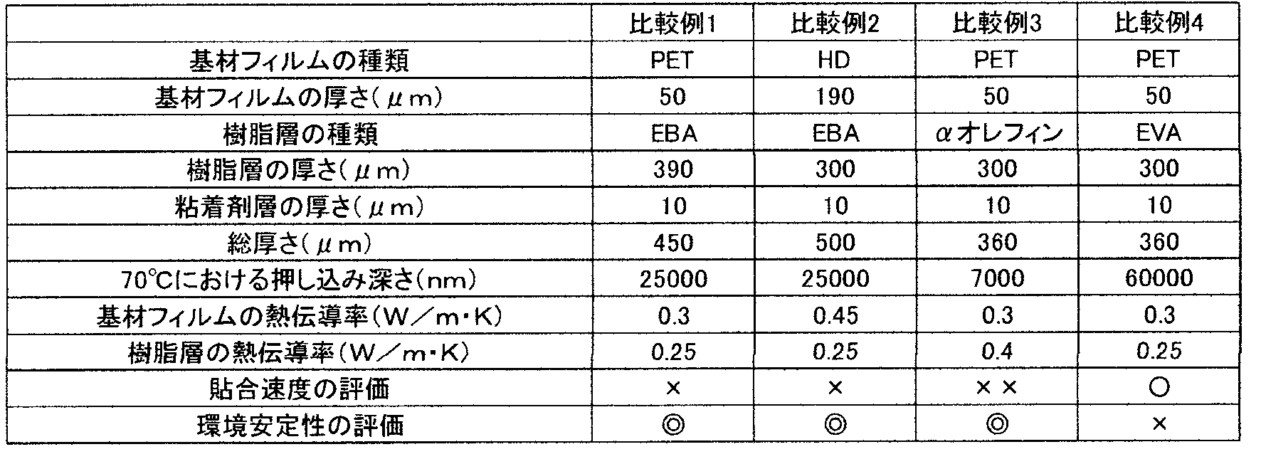
表1に示すように、実施例1~6は、ナノインデンターを用いISO14577に準拠して測定される70℃における圧子の押し込み深さが15000nm~50000nmであり、樹脂層の厚みが240μm~300μmで、総厚みが440μm以下であるため、貼合速度および環境安定性の評価において良好な結果となった。特に、実施例3は、樹脂層の70℃における熱伝導率が0.7W/m・Kと他の実施例より高いため、貼合速度の評価において優良な結果となった。また、実施例4,5は、電子部品用テープの総厚みが310μmと他の実施例よりも薄いため、貼合速度の評価において優良な結果となった。実施例6は環境安定性において、実施例1~5には劣るものの、ナノインデンターを用いて測定される70℃での押し込み深さが50000nmと大きいため貼合速度の評価において良好な結果となった。
一方、表2に示すように、比較例1は樹脂層の厚みが300μmを超え、比較例2は総厚みが450μmを超えるため、貼合速度の評価において劣る結果となった。比較例3は、ナノインデンターを用いISO14577に準拠して測定される70℃における圧子の押し込み深さが10000nm未満であるため、貼合速度の評価において劣る結果となった。比較例4は、ナノインデンターを用いISO14577に準拠して測定される70℃における圧子の押し込み深さが50000nmを超えるため、環境安定性の評価において劣る結果となった。
1:電子部品用テープ
2:基材フィルム
3:樹脂層
4:粘着剤層
5:剥離フィルム
6:半導体ウエハ
61:凹凸
7:研削機
2:基材フィルム
3:樹脂層
4:粘着剤層
5:剥離フィルム
6:半導体ウエハ
61:凹凸
7:研削機
Claims (6)
- 少なくとも一層の樹脂層を有し、
前記樹脂層は、ナノインデンターを用いISO14577に準拠して測定される60℃~80℃のいずれかの温度における前記ナノインデンターの圧子の押し込み深さが10000nm~50000nmであり、
前記樹脂層の厚みが50μm~300μmで、総厚みが450μm以下であることを特徴とする電子部品用テープ。 - 前記樹脂層は、60~80℃での熱伝導率が、少なくとも0.30W/m・K以上であることを特徴とする請求項1に記載の電子部品用テープ。
- 10μm以上の段差が設けられている半導体ウエハの回路形成面に貼合されることを特徴とする請求項1または請求項2に記載の電子部品用テープ。
- 前記樹脂層の厚みが前記段差の1倍以上2倍以下であることを特徴とする請求項3に記載の電子部品用テープ。
- 10μm以上の段差が設けられている半導体ウエハの回路形成面に、請求項1から請求項3のいずれか一項に記載の電子部品用テープを50~100℃の温度で貼合する貼合工程と、
前記貼合工程の後に、前記半導体ウエハの回路形成面とは反対側の面を研削する研削工程とを有することを特徴とする電子部品の加工方法。 - 前記貼合工程における貼合速度が3mm/S以上であることを特徴とする請求項5に記載の電子部品の加工方法。
Priority Applications (2)
| Application Number | Priority Date | Filing Date | Title |
|---|---|---|---|
| KR1020207028418A KR102466287B1 (ko) | 2019-04-08 | 2020-03-24 | 전자 부품용 테이프, 및 전자 부품의 가공 방법 |
| CN202080002305.XA CN112055735B (zh) | 2019-04-08 | 2020-03-24 | 电子部件用胶带及电子部件的加工方法 |
Applications Claiming Priority (2)
| Application Number | Priority Date | Filing Date | Title |
|---|---|---|---|
| JP2019-073512 | 2019-04-08 | ||
| JP2019073512A JP6678796B1 (ja) | 2019-04-08 | 2019-04-08 | 電子部品用テープおよび電子部品の加工方法 |
Publications (1)
| Publication Number | Publication Date |
|---|---|
| WO2020209043A1 true WO2020209043A1 (ja) | 2020-10-15 |
Family
ID=70057933
Family Applications (1)
| Application Number | Title | Priority Date | Filing Date |
|---|---|---|---|
| PCT/JP2020/012847 Ceased WO2020209043A1 (ja) | 2019-04-08 | 2020-03-24 | 電子部品用テープおよび電子部品の加工方法 |
Country Status (5)
| Country | Link |
|---|---|
| JP (1) | JP6678796B1 (ja) |
| KR (1) | KR102466287B1 (ja) |
| CN (1) | CN112055735B (ja) |
| TW (1) | TWI764114B (ja) |
| WO (1) | WO2020209043A1 (ja) |
Families Citing this family (2)
| Publication number | Priority date | Publication date | Assignee | Title |
|---|---|---|---|---|
| JP2024126165A (ja) * | 2023-03-07 | 2024-09-20 | アールエム東セロ株式会社 | 粘着性フィルムおよび電子装置の製造方法 |
| KR20250056080A (ko) * | 2023-10-18 | 2025-04-25 | 주식회사 엘지화학 | 표면 보호 필름 |
Citations (3)
| Publication number | Priority date | Publication date | Assignee | Title |
|---|---|---|---|---|
| JP2009269940A (ja) * | 2008-04-30 | 2009-11-19 | Nikon Corp | 携帯機器用外装膜、携帯機器用外装部材、及び携帯機器用塗料 |
| JP2011187832A (ja) * | 2010-03-10 | 2011-09-22 | Hitachi Maxell Ltd | ウェハ裏面研削用粘着シート、その製造方法及びその使用方法 |
| JP2012167247A (ja) * | 2011-01-25 | 2012-09-06 | Hitachi Maxell Ltd | 防水用両面粘着テープ |
Family Cites Families (8)
| Publication number | Priority date | Publication date | Assignee | Title |
|---|---|---|---|---|
| JP4054113B2 (ja) | 1998-06-25 | 2008-02-27 | 三井化学株式会社 | 半導体ウエハの裏面研削用粘着フィルム及びそれを用いる半導体ウエハの裏面研削方法 |
| JP3773358B2 (ja) | 1998-07-01 | 2006-05-10 | 三井化学株式会社 | 半導体ウエハの裏面研削用粘着フィルム及びそれを用いる半導体ウエハの裏面研削方法 |
| WO2011105217A1 (ja) * | 2010-02-23 | 2011-09-01 | 株式会社 きもと | 粘着シート |
| JP5242830B1 (ja) | 2012-07-06 | 2013-07-24 | 古河電気工業株式会社 | 半導体ウェハ表面保護用粘着テープおよび半導体ウェハの製造方法 |
| JP6528259B2 (ja) * | 2014-08-19 | 2019-06-12 | リンテック株式会社 | 表面保護フィルム |
| JP6490459B2 (ja) * | 2015-03-13 | 2019-03-27 | 古河電気工業株式会社 | ウェハ固定テープ、半導体ウェハの処理方法および半導体チップ |
| SG11201804425RA (en) * | 2016-03-03 | 2018-09-27 | Lintec Corp | Adhesive tape for semiconductor processing and method for producing semiconductor device |
| JP7079200B2 (ja) * | 2017-03-31 | 2022-06-01 | 古河電気工業株式会社 | 半導体ウェハ表面保護用粘着テープ及び半導体ウェハの加工方法 |
-
2019
- 2019-04-08 JP JP2019073512A patent/JP6678796B1/ja active Active
-
2020
- 2020-03-23 TW TW109109561A patent/TWI764114B/zh active
- 2020-03-24 WO PCT/JP2020/012847 patent/WO2020209043A1/ja not_active Ceased
- 2020-03-24 KR KR1020207028418A patent/KR102466287B1/ko active Active
- 2020-03-24 CN CN202080002305.XA patent/CN112055735B/zh active Active
Patent Citations (3)
| Publication number | Priority date | Publication date | Assignee | Title |
|---|---|---|---|---|
| JP2009269940A (ja) * | 2008-04-30 | 2009-11-19 | Nikon Corp | 携帯機器用外装膜、携帯機器用外装部材、及び携帯機器用塗料 |
| JP2011187832A (ja) * | 2010-03-10 | 2011-09-22 | Hitachi Maxell Ltd | ウェハ裏面研削用粘着シート、その製造方法及びその使用方法 |
| JP2012167247A (ja) * | 2011-01-25 | 2012-09-06 | Hitachi Maxell Ltd | 防水用両面粘着テープ |
Also Published As
| Publication number | Publication date |
|---|---|
| TWI764114B (zh) | 2022-05-11 |
| TW202045658A (zh) | 2020-12-16 |
| JP2020174064A (ja) | 2020-10-22 |
| KR102466287B1 (ko) | 2022-11-14 |
| CN112055735A (zh) | 2020-12-08 |
| CN112055735B (zh) | 2022-11-18 |
| KR20200126415A (ko) | 2020-11-06 |
| JP6678796B1 (ja) | 2020-04-08 |
Similar Documents
| Publication | Publication Date | Title |
|---|---|---|
| JP5117629B1 (ja) | ウェハ加工用粘着テープ | |
| JP7079200B2 (ja) | 半導体ウェハ表面保護用粘着テープ及び半導体ウェハの加工方法 | |
| JP5055097B2 (ja) | 検査用粘着シート | |
| JP6053909B2 (ja) | 半導体ウエハ表面保護用粘着テープおよびその製造方法 | |
| KR102290466B1 (ko) | 필름상 소성 재료, 및 지지 시트를 가지는 필름상 소성 재료 | |
| JP2014192464A (ja) | 半導体ウェハ表面保護用粘着テープ | |
| JP2015185691A (ja) | 半導体ウェハ加工用粘着テープ、該粘着テープの製造方法および半導体ウェハの加工方法 | |
| JP5697061B1 (ja) | 半導体ウェハ加工用粘着テープおよび半導体ウェハの加工方法 | |
| CN112055736B (zh) | 电子部件用胶带及电子部件的加工方法 | |
| JP5100902B1 (ja) | 半導体ウエハ表面保護用粘着テープ | |
| JP6678796B1 (ja) | 電子部品用テープおよび電子部品の加工方法 | |
| TW201927964A (zh) | 工件加工用片材及加工畢工件之製造方法 | |
| KR102267114B1 (ko) | 반도체 가공용 점착 테이프 | |
| KR20170128210A (ko) | 반도체 웨이퍼 가공용 점착 테이프 | |
| JP5863873B2 (ja) | 半導体ウェハの裏面研削加工用表面保護粘着テープおよび半導体ウェハの研削加工方法 | |
| WO2017068659A1 (ja) | 半導体ウェハの裏面研削加工用表面保護粘着テープおよび半導体ウェハの研削加工方法 | |
| JP5764600B2 (ja) | 半導体ウェハの裏面研削加工用表面保護粘着テープおよび半導体ウェハの加工方法 | |
| JP5255717B1 (ja) | 半導体加工用表面保護粘着テープ | |
| JP2025152519A (ja) | 半導体ウェハ表面保護用テープ | |
| TW201714997A (zh) | 半導體晶圓之內面硏磨加工用表面保護黏著帶及半導體晶圓之硏磨加工方法 |
Legal Events
| Date | Code | Title | Description |
|---|---|---|---|
| ENP | Entry into the national phase |
Ref document number: 20207028418 Country of ref document: KR Kind code of ref document: A |
|
| 121 | Ep: the epo has been informed by wipo that ep was designated in this application |
Ref document number: 20787616 Country of ref document: EP Kind code of ref document: A1 |
|
| NENP | Non-entry into the national phase |
Ref country code: DE |
|
| 122 | Ep: pct application non-entry in european phase |
Ref document number: 20787616 Country of ref document: EP Kind code of ref document: A1 |