WO2020204073A1 - 硬化膜形成用組成物、波長変換膜、発光表示素子、及び波長変換膜の形成方法 - Google Patents
硬化膜形成用組成物、波長変換膜、発光表示素子、及び波長変換膜の形成方法 Download PDFInfo
- Publication number
- WO2020204073A1 WO2020204073A1 PCT/JP2020/015031 JP2020015031W WO2020204073A1 WO 2020204073 A1 WO2020204073 A1 WO 2020204073A1 JP 2020015031 W JP2020015031 W JP 2020015031W WO 2020204073 A1 WO2020204073 A1 WO 2020204073A1
- Authority
- WO
- WIPO (PCT)
- Prior art keywords
- group
- forming
- composition
- cured film
- wavelength conversion
- Prior art date
- Legal status (The legal status is an assumption and is not a legal conclusion. Google has not performed a legal analysis and makes no representation as to the accuracy of the status listed.)
- Ceased
Links
Images

Classifications
-
- B—PERFORMING OPERATIONS; TRANSPORTING
- B82—NANOTECHNOLOGY
- B82Y—SPECIFIC USES OR APPLICATIONS OF NANOSTRUCTURES; MEASUREMENT OR ANALYSIS OF NANOSTRUCTURES; MANUFACTURE OR TREATMENT OF NANOSTRUCTURES
- B82Y20/00—Nanooptics, e.g. quantum optics or photonic crystals
-
- C—CHEMISTRY; METALLURGY
- C08—ORGANIC MACROMOLECULAR COMPOUNDS; THEIR PREPARATION OR CHEMICAL WORKING-UP; COMPOSITIONS BASED THEREON
- C08F—MACROMOLECULAR COMPOUNDS OBTAINED BY REACTIONS ONLY INVOLVING CARBON-TO-CARBON UNSATURATED BONDS
- C08F290/00—Macromolecular compounds obtained by polymerising monomers on to polymers modified by introduction of aliphatic unsaturated end or side groups
- C08F290/02—Macromolecular compounds obtained by polymerising monomers on to polymers modified by introduction of aliphatic unsaturated end or side groups on to polymers modified by introduction of unsaturated end groups
- C08F290/06—Polymers provided for in subclass C08G
-
- C—CHEMISTRY; METALLURGY
- C09—DYES; PAINTS; POLISHES; NATURAL RESINS; ADHESIVES; COMPOSITIONS NOT OTHERWISE PROVIDED FOR; APPLICATIONS OF MATERIALS NOT OTHERWISE PROVIDED FOR
- C09D—COATING COMPOSITIONS, e.g. PAINTS, VARNISHES OR LACQUERS; FILLING PASTES; CHEMICAL PAINT OR INK REMOVERS; INKS; CORRECTING FLUIDS; WOODSTAINS; PASTES OR SOLIDS FOR COLOURING OR PRINTING; USE OF MATERIALS THEREFOR
- C09D175/00—Coating compositions based on polyureas or polyurethanes; Coating compositions based on derivatives of such polymers
- C09D175/04—Polyurethanes
- C09D175/14—Polyurethanes having carbon-to-carbon unsaturated bonds
-
- C—CHEMISTRY; METALLURGY
- C09—DYES; PAINTS; POLISHES; NATURAL RESINS; ADHESIVES; COMPOSITIONS NOT OTHERWISE PROVIDED FOR; APPLICATIONS OF MATERIALS NOT OTHERWISE PROVIDED FOR
- C09D—COATING COMPOSITIONS, e.g. PAINTS, VARNISHES OR LACQUERS; FILLING PASTES; CHEMICAL PAINT OR INK REMOVERS; INKS; CORRECTING FLUIDS; WOODSTAINS; PASTES OR SOLIDS FOR COLOURING OR PRINTING; USE OF MATERIALS THEREFOR
- C09D201/00—Coating compositions based on unspecified macromolecular compounds
- C09D201/02—Coating compositions based on unspecified macromolecular compounds characterised by the presence of specified groups, e.g. terminal or pendant functional groups
-
- C—CHEMISTRY; METALLURGY
- C09—DYES; PAINTS; POLISHES; NATURAL RESINS; ADHESIVES; COMPOSITIONS NOT OTHERWISE PROVIDED FOR; APPLICATIONS OF MATERIALS NOT OTHERWISE PROVIDED FOR
- C09D—COATING COMPOSITIONS, e.g. PAINTS, VARNISHES OR LACQUERS; FILLING PASTES; CHEMICAL PAINT OR INK REMOVERS; INKS; CORRECTING FLUIDS; WOODSTAINS; PASTES OR SOLIDS FOR COLOURING OR PRINTING; USE OF MATERIALS THEREFOR
- C09D7/00—Features of coating compositions, not provided for in group C09D5/00; Processes for incorporating ingredients in coating compositions
- C09D7/40—Additives
- C09D7/60—Additives non-macromolecular
- C09D7/61—Additives non-macromolecular inorganic
-
- C—CHEMISTRY; METALLURGY
- C09—DYES; PAINTS; POLISHES; NATURAL RESINS; ADHESIVES; COMPOSITIONS NOT OTHERWISE PROVIDED FOR; APPLICATIONS OF MATERIALS NOT OTHERWISE PROVIDED FOR
- C09D—COATING COMPOSITIONS, e.g. PAINTS, VARNISHES OR LACQUERS; FILLING PASTES; CHEMICAL PAINT OR INK REMOVERS; INKS; CORRECTING FLUIDS; WOODSTAINS; PASTES OR SOLIDS FOR COLOURING OR PRINTING; USE OF MATERIALS THEREFOR
- C09D7/00—Features of coating compositions, not provided for in group C09D5/00; Processes for incorporating ingredients in coating compositions
- C09D7/40—Additives
- C09D7/60—Additives non-macromolecular
- C09D7/61—Additives non-macromolecular inorganic
- C09D7/62—Additives non-macromolecular inorganic modified by treatment with other compounds
-
- G—PHYSICS
- G02—OPTICS
- G02B—OPTICAL ELEMENTS, SYSTEMS OR APPARATUS
- G02B5/00—Optical elements other than lenses
- G02B5/20—Filters
Definitions
- the present invention relates to a composition for forming a cured film, a wavelength conversion film, a light emitting display element, and a method for forming a wavelength conversion film.
- semiconductor nanoparticles obtained by forming semiconductors such as cadmium sulfide (CdS), cadmium telluride (CdTe), and indium phosphide (InP) to a nanometer size have been attracting attention. Since such semiconductor nanoparticles exhibit broad optical absorption and special optical characteristics of emitting fluorescence with a narrow spectrum width, various applications are currently being studied. For example, the above-mentioned semiconductor nanoparticles have come to be used for displays and illuminations using organic electroluminescence (EL) elements, micro-sized light emitting diode elements (micro LED elements), and the like (Japanese Patent Laid-Open No. 2014-174406). See Gazette).
- EL organic electroluminescence
- micro LED elements micro-sized light emitting diode elements
- a method of forming a wavelength conversion film containing semiconductor nanoparticles by coating a curable composition containing semiconductor nanoparticles is widely used.
- a composition containing semiconductor nanoparticles, a polymerizable compound, a polymerization initiator, a polymer and the like is known (see JP-A-2015-28139).
- the polymerizable compound a polyfunctional acrylate such as 1,9-nonanediol diacrylate is used.
- the composition for forming the wavelength conversion film is required to have fluorescence performance such as a high fluorescence quantum yield in the obtained wavelength conversion film and a narrow half-value width of the fluorescence spectrum.
- a wavelength conversion film may be cured by heating, and it is important that the wavelength conversion film has good fluorescence performance even when the wavelength conversion film is obtained by heating.
- the composition has good dispersion stability and coatability.
- the conventional compositions containing semiconductor nanoparticles and using polyfunctional acrylate as the polymerizable compound are still improved in terms of the fluorescence performance of these obtained wavelength conversion films and the handleability of the composition. There is room for.
- the present invention has been made based on the above circumstances, and is a cured film-forming composition having good dispersion stability and coatability, and also good fluorescence performance of the obtained wavelength conversion film. It is an object of the present invention to provide a wavelength conversion film and a light emitting display element formed from a composition for forming a cured film, and a method for forming the wavelength conversion film.
- the invention made to solve the above problems is a composition for forming a cured film containing (A) semiconductor nanoparticles and (B) urethane (meth) acrylate having a plurality of polymerizable groups.
- Another invention made to solve the above problems is a wavelength conversion film formed from the cured film forming composition.
- Yet another invention made to solve the above problems is a light emitting display device provided with the wavelength conversion film.
- Yet another invention made to solve the above problems includes a step of directly or indirectly forming a coating film on a substrate and a step of heating the coating film, and the coating film is composed of the cured film forming composition.
- This is a method for forming a wavelength conversion film formed of an object.
- a cured film-forming composition having good dispersion stability and coatability, and also having good fluorescence performance of the obtained wavelength conversion film, and a wavelength formed from such a cured film-forming composition. It is possible to provide a conversion film, a light emitting display element, and a method for forming the wavelength conversion film.
- FIG. 1 is a cross-sectional view schematically showing a light emitting display element according to an embodiment of the present invention.
- the composition for forming a cured film according to an embodiment of the present invention contains (A) semiconductor nanoparticles and (B) urethane (meth) acrylate having a plurality of polymerizable groups.
- the cured film-forming composition by using (B) urethane (meth) acrylate as a polymerizable compound together with (A) semiconductor nanoparticles, dispersion stability and coatability are improved, and wavelength conversion can be obtained.
- the fluorescence performance of the film is also good.
- the wavelength conversion film obtained from the cured film forming composition has a high fluorescence quantum yield and a narrow half width of the fluorescence spectrum.
- the narrower the half width of the fluorescence spectrum the more the wavelength can be converted into fluorescence with high color purity.
- the wavelength conversion film formed from the cured film forming composition has a sufficient fluorescence quantum yield even after being heat-treated.
- the cured film-forming composition preferably further contains one or both of (C) light diffusing particles and (D) polymer in order to improve dispersion stability, coatability, fluorescence performance, and the like.
- the cured film-forming composition can further contain (E) an antioxidant, (F) a dispersion medium, (G) a radiation-sensitive compound, and the like.
- (A) Semiconductor nanoparticles) (A) Semiconductor nanoparticles have nanocrystals containing a semiconductor substance.
- the semiconductor nanoparticles (A) preferably have a ligand that covers at least a part of the nanocrystals.
- the semiconductor nanoparticles can be particles containing semiconductors and having an average particle size of 1 nm or more and 1,000 nm or less. The average particle size is an arithmetic mean value of diameters measured using a transmission electron microscope (TEM) for 20 arbitrarily selected particles.
- TEM transmission electron microscope
- the above-mentioned diameter means an average value ((major axis + minor axis) / 2) of a major axis and a minor axis (diameter orthogonal to the major axis) (hereinafter, the same applies to the average particle size).
- Nanocrystals are crystals containing semiconductor substances. Examples of the material constituting the nanocrystal include Group 2 element, Group 11 element, Group 12 element, Group 13 element, Group 14 element, Group 15 element, Group 16 element, and a compound containing a combination thereof.
- Examples of the above elements include Be (berylium), Mg (magnium), Ca (calcium), Sr (strontium), Ba (barium), Cu (copper), Ag (silver), Au (gold), Zn (zinc). , B (boron), Al (aluminum), Ga (gallium), In (indium), Tell (talium), C (carbon), Si (silicon), Ge (germanium), Sn (tin), N (nitrogen) , P (phosphorus), As (arsenic), Sb (antimony), Bi (bismuth), O (oxygen), S (silicon), Se (selenium), Te (tellurium), Po (polonium) and the like.
- the nanocrystal preferably contains at least two or more elements selected from the group consisting of Group 2 elements, Group 11 elements, Group 12 elements, Group 13 elements, Group 14 elements, Group 15 elements and Group 16 elements. Further, the nanocrystal preferably contains a Group 13 element (Al, Ga, In, etc.), and more preferably contains In.
- the semiconductor material constituting the nanocrystal include BN, BP, BAs, AlN, AlP, AlAs, GaN, GaAs, GaSb, InN, InP, InAs, InSb and the like.
- the semiconductor substance a compound of a Group 13 element (Al, Ga, In, etc.) and a Group 15 element (N, P, As, etc.) is preferable, and InP is more preferable.
- the nanocrystal may be a homogeneous structure type composed of one kind of compound or a core-shell type composed of two or more kinds of compounds.
- Core-shell nanocrystals are constructed by forming a core structure with one type of compound and coating the core structure with another type of compound. For example, by coating the semiconductor of the core with a semiconductor having a larger bandgap, excitons (electron-hole pairs) generated by photoexcitation are confined in the core. As a result, the probability of non-radiative transition on the nanocrystal surface is reduced and the fluorescence quantum yield is improved.
- the core is at least two or more selected from the group consisting of Group 2 elements, Group 11 elements, Group 12 elements, Group 13 elements, Group 14 elements, Group 15 elements and Group 16 elements. It is preferably a semiconductor material containing an element. Further, the core is more preferably a semiconductor substance which is a compound of a group 13 element and a group 15 element, or a semiconductor substance containing In, and particularly preferably InP. On the other hand, the shell is preferably a compound containing a Group 12 element (Zn, Cd, etc.) and a Group 16 element (S, Se, etc.), and more preferably ZnS.
- core-shell type nanocrystals examples include InP / ZnS, InP / ZnSe, CuInS 2 / ZnS and (ZnS / AgInS 2 ) solid solution / ZnS, and InP / ZnS is preferable.
- the InP / ZnS is a nanocrystal having InP as a core and ZnS as a shell (the same applies to other notations), and the core-shell type nanocrystal is a core / multi-layer shell type nanocrystal.
- InP / ZnSe / ZnS, InP / GaP / ZnS, and the like can be mentioned.
- InP is the core and the others are shells.
- InP / ZnSe / ZnS is preferable.
- a known method such as thermal decomposition of an organometallic compound in a coordinating organic solvent can be used.
- a precursor for forming a shell on the core surface is added to the reaction system to form a shell on the core surface, and then the reaction is carried out. It is obtained by stopping and separating from the solvent.
- the method of controlling the average particle size of nanocrystals include a method of adjusting the reaction temperature, reaction time, and the like. It is also possible to use a commercially available product.
- InP / ZnS which is a core-shell type nanocrystal, can also be synthesized by referring to, for example, the method described in the technical document "Chemistry of Materials. 2015, 27, 4893-4898".
- the ligand coats at least a portion of the nanocrystal.
- the ligand electrostatically stabilizes the surface of the nanocrystal.
- the ligands are carboxy group (-COOH), thiol group (-SH), phosphono group (-PO (OH) 2 ), amide group (-CONR 2 or -CONCOR: R, respectively, each of which is a hydrogen atom or hydrocarbon. It is preferable to have a group x which is a group) or a combination thereof. These groups, ions (e.g., -COO -) may be present in the form of. Since the group x is well adsorbed on the surface of the nanocrystal, good dispersibility can be exhibited. Among the groups x, a carboxy group and a thiol group are preferable, and a thiol group is more preferable.
- the ether group (-O-), the ester group (-COO-), and the siloxane group (-SiR 2- O-: R are each independently a hydrogen atom or a hydrocarbon group. ) Or a combination thereof, which is preferably a first ligand having a group y.
- the group y is a group that exhibits good dispersibility with respect to the (F) dispersion medium, particularly the polar dispersion medium.
- an ether group and an ester group are preferable, and an ether group is more preferable.
- the first ligand is preferably one represented by the following formula (4).
- X is a carboxy group, a group represented by the following formula (a), a group represented by the following formula (b), a thiol group, a phosphono group or an amide group.
- Y is a single bond, an oxygen atom or a sulfur atom.
- Z is an ether group (oxygen atom), an ester group or a siloxane group.
- R 6 is a divalent chain hydrocarbon group having 1 to 5 carbon atoms.
- R 7 is a monovalent chain hydrocarbon group having 1 to 8 carbon atoms.
- r is a natural number. When r is 2 or more, the plurality of R 6s and Z may be the same or different from each other.
- a carboxy group a group represented by the above formula (a), a group represented by the above formula (b), and a thiol group are preferable, and a thiol group is more preferable.
- Y a single bond and a sulfur atom are preferable, and a single bond is preferable.
- X is a thiol group, a phosphono group or an amide group
- Y is preferably a single bond.
- an ether group and an ester group are preferable, and an ether group is more preferable.
- Z is an ether group
- ⁇ (R 6 ⁇ Z) r ⁇ R 7 in the formula (1) forms a polyoxyalkylene chain.
- R 6 a divalent chain hydrocarbon group having 2 to 4 carbon atoms is preferable, and a divalent chain hydrocarbon group having 2 carbon atoms is more preferable.
- R 6 is preferably an alkanediyl group, most preferably an ethane-1,2-diyl group.
- Examples of the monovalent chain hydrocarbon group having 1 to 8 carbon atoms represented by R 7, methyl group, an ethyl group, an alkyl group such as propyl, ethenyl, alkenyl groups such as propenyl group and an ethynyl group, Alkinyl groups such as, etc. can be mentioned, but alkyl groups are preferable.
- the carbon number of R 7 is preferably 5 or less, more preferably 3 or less, and even more preferably 1. That is, as R 7 , a methyl group is most preferable. When the number of carbon atoms of R 7 is small, the dispersibility in the polar dispersion medium is further improved.
- the upper limit of r in the above formula (4) is, for example, 500, preferably 50.
- the lower limit of r is 1, but 2 is preferable, and 5 is more preferable.
- a second ligand having a hydrocarbon group (group z) having 6 to 20 carbon atoms may be used together with the above group x. Since the group z is a group that exhibits particularly good dispersibility with respect to a non-polar dispersion medium, a dispersion medium in which both a polar dispersion medium and a non-polar dispersion medium coexist by using a first ligand and a second ligand in combination. Among them, (A) the dispersibility of the semiconductor nanoparticles is further improved. Further, by using the second ligand, the compatibility with other components when forming the wavelength conversion film can be enhanced.
- the group x of the second ligand is the same as the group x of the first ligand, and is a group that can be adsorbed well on the surface of the nanocrystal.
- As the group x contained in the second ligand a carboxy group and a thiol group are preferable, and a thiol group is more preferable.
- Examples of the hydrocarbon group having 6 to 20 carbon atoms which is a group z, include an aliphatic hydrocarbon group such as an alkyl group, an alkenyl group, an alkynyl group and a cycloalkyl group, and an aromatic hydrocarbon group such as a phenyl group and a naphthyl group.
- an aliphatic hydrocarbon group is preferable, and an alkyl group is more preferable.
- As the lower limit of the number of carbon atoms of the group z 8 is preferable, and 10 is more preferable.
- As the upper limit of the number of carbon atoms 18 is preferable, and 16 is more preferable.
- the first ligand and the second ligand can be coordinated to the surface of the nanocrystal by a conventionally known method.
- These ligands are used when synthesizing nanocrystals and may be ligands attached (coordinated) to the surface of the nanocrystals, or coordinated to the surface of the nanocrystals by ligand exchange after synthesizing the nanocrystals. It may be made to. However, the ligand is not completely exchanged even by the ligand exchange, and the original ligand and the new ligand may coexist.
- both the first ligand and the second ligand are usually coordinated on the surface of the nanocrystal. It becomes a state.
- the lower limit of the content of the first ligand with respect to the total content of the first ligand and the second ligand is preferably 30% by mass, more preferably 50% by mass, still more preferably 60% by mass.
- the upper limit of the content of the first ligand with respect to the total content of the first ligand and the second ligand may be 99% by mass or 90% by mass.
- the content of the first ligand in the total ligands of the (A) semiconductor nanoparticles is also preferably within the above range.
- the content of the ligand such as the first ligand in the (A) semiconductor nanoparticles can be measured by the method described in Examples described later.
- the lower limit of the average particle size of the semiconductor nanoparticles is preferably 0.5 nm, more preferably 1.0 nm.
- the upper limit of the average particle size is preferably 20 nm, more preferably 10 nm.
- the wavelength region of fluorescence of (A) semiconductor nanoparticles can be controlled by appropriately selecting the constituent materials and average particle diameter of the nanocrystals.
- the shape of the nanocrystal is not particularly limited, and may be, for example, spherical, rod-shaped, disk-shaped, or other shape, but spherical or rod-shaped is preferable. If the semiconductor nanoparticles are spherical, the surface energy of the particles becomes small, so that the dispersion stability can be improved. Further, if the semiconductor nanoparticles are rod-shaped, the light utilization efficiency can be improved by polarized light emission.
- the lower limit of the content of the (A) semiconductor nanoparticles in the total solid content of the cured film forming composition is preferably 1% by mass, more preferably 5% by mass, and even more preferably 8% by mass.
- the upper limit of this content is preferably 50% by mass, more preferably 30% by mass, and even more preferably 20% by mass.
- the solid content means a component other than the (F) dispersion medium.
- (B) Urethane (meth) acrylate) (B) Urethane (meth) acrylate has a plurality of polymerizable groups.
- the urethane (meth) acrylate refers to a (meth) acrylate having a urethane bond (-NHCOO-).
- the urethane (meth) acrylate has a (meth) acryloyl group as a polymerizable group, but may further have other polymerizable groups such as an epoxy group and a vinyl group.
- the lower limit of the number of polymerizable groups contained in the urethane (meth) acrylate may be 2, but 4 is preferable, 6 is more preferable, 8 is more preferable, 9 is more preferable, and 10 is more preferable. More preferably, 12 is particularly preferable.
- the upper limit of the number of the polymerizable groups is, for example, 30, preferably 24, and more preferably 18.
- the urethane (meth) acrylate (B) preferably has an isocyanuric acid structure, a triazine structure, or a combination thereof.
- B When the urethane (meth) acrylate has such a structure, the coatability, dispersion stability, fluorescence performance of the obtained wavelength conversion film, and the like are improved.
- the isocyanuric acid structure include a structure represented by the following formula (5).
- Examples of the triazine structure include a structure represented by the following formula (6).
- the lower limit of the molecular weight of the urethane (meth) acrylate (B) is, for example, 300, preferably 600, more preferably 1,000, and even more preferably 1,800.
- the upper limit of this molecular weight is, for example, 10,000, preferably 6,000, more preferably 5,000, and even more preferably 4,000.
- R 1 is an m-valent organic group having 1 to 60 carbon atoms.
- a plurality of R 2 are each independently a group containing one or more (meth) acryloyl groups.
- m is 2 or 3.
- An organic group is a group containing one or more carbon atoms.
- Examples of the m-valent organic group having 1 to 60 carbon atoms represented by R 1 include an m-valent hydrocarbon group and a group in which a part or all of the hydrogen atoms of the m-valent hydrocarbon group are substituted with a substituent. Examples thereof include a group containing a group containing CO, CS, O, S, NR'or a combination of two or more of these between carbon-carbon of an m-valent hydrocarbon group. R'is a hydrogen atom or a hydrocarbon group having 1 to 6 carbon atoms. Examples of the above-mentioned hydrocarbon group include a chain hydrocarbon group, an alicyclic hydrocarbon group, an aromatic hydrocarbon group, and a group composed of a combination thereof.
- substituents examples include a hydroxy group, a carboxy group, an amino group, a cyano group, a nitro group, a sulfonamide group and the like.
- substituents examples include a hydroxy group, a carboxy group, an amino group, a cyano group, a nitro group, a sulfonamide group and the like.
- group in which two or more of CO, CS, O, S and NR'are combined include -COO-, -CONR'-, -NR' COO- and the like.
- the lower limit of the number of carbon atoms of the organic group represented by R 1 , 4 is preferable, 10 is more preferable, and 16 is further preferable.
- the upper limit of the number of carbon atoms 50 is preferable, 40 is more preferable, and 30 is further preferable.
- M is preferably 3.
- the m-valent organic group having 1 to 60 carbon atoms represented by R 1 is preferably a group containing a heterocyclic structure, and more preferably a group containing a heterocyclic structure containing nitrogen.
- the nitrogen-containing heterocyclic structure include a triazine structure and an isocyanuric acid structure.
- M-valent organic group having 1 to 60 carbon atoms represented by R 1 is a group consisting of only heterocyclic structure containing nitrogen, and the hydrocarbon group (more preferably a heterocyclic structure containing a nitrogen chain hydrocarbon group ) Is preferred.
- R 1 examples include groups represented by the following formulas (3-1) and (3-2), and in particular, a group represented by formula (3-1) is preferable.
- R 1 is represented by the following formula (3-1) or (3-2), m is 3.
- the plurality of R 5 each independently, an alkanediyl group having a single bond or a C 1-12.
- alkanediyl group As the R 5, alkanediyl group. As the lower limit of the number of carbon atoms of this alkanediyl group, 2 is preferable, and 4 is more preferable. On the other hand, as the upper limit of the number of carbon atoms, 10 is preferable, and 8 is more preferable.
- the alkanediyl group may be linear or branched, but is preferably linear.
- R 2 is a group containing one or more (meth) acryloyl groups, and forms a urethane bond in the formula (1) via a polyvalent organic group according to the number of one or more (meth) acryloyloxy groups. It is preferably a group that binds to the contained oxygen atom. Having a group represented by R 2 (meth) is not particularly limited as the number of acryloyl groups, 2 is preferable as the lower limit, 3 is more preferable. On the other hand, the upper limit is preferably 10 and more preferably 5.
- Suitable R 2 includes a group represented by the following formula (2).
- R 3 is a single bond or an alkanediyl group having 1 to 3 carbon atoms.
- R 4 is a (meth) acryloyl groups.
- n is 1 or 2.
- p is 0 or 1.
- q is an integer of 1 to 3.
- the R 3 preferably alkanediyl group having 1 to 3 carbon atoms, methylene bridge is more preferable.
- the R 4, acryloyl group is preferred.
- n 2 is preferable for n.
- the p is preferably 1.
- q is preferably 3.
- (B) urethane (meth) acrylate examples include U-6HA, UA-1100H, U-6LPA, U-15HA, U-6H, U-10HA, U-10PA, Shin Nakamura Chemical Industry Co., Ltd. UA-53H, UA-33H, UN-904 of Negami Kogyo Co., Ltd., UA-306H of Kyoeisha Chemical Co., Ltd., UA-306T, UA-306I, UA-510H, Laromer UA-9048 of BASF, UA- Examples thereof include 9050, PR9052, EBECRYL 220, 5129, 8301, KRM8200, 8200AE, 8452 of Daicel Ornex Co., Ltd.
- the lower limit of the content of (B) urethane (meth) acrylate 50 parts by mass is preferable, 100 parts by mass is more preferable, and 200 parts by mass is further preferable with respect to 100 parts by mass of (A) semiconductor nanoparticles.
- the upper limit of this content is preferably 1,000 parts by mass, more preferably 500 parts by mass, and even more preferably 400 parts by mass.
- the light diffusing particles are components that increase the fluorescence quantum yield (wavelength conversion efficiency) by increasing the amount of light incident on the semiconductor nanoparticles by light diffusion.
- the fluorescence quantum yield can be further increased.
- Light-diffusing particles differ from semiconductor nanoparticles in that they do not fluoresce.
- the light diffusing particles (C) preferably contain a metal oxide, and more preferably metal oxide particles.
- metal oxides Al 2 O 3 , SiO 2 , ZnO, ZrO 2 , BaTIO 3 , TIO 2 , Ta 2 O 5 , Ti 3 O 5 , ITO (tin-doped indium oxide), IZO (zinc-doped) Indium oxide), ATO (antimony-doped tin oxide), AZO (aluminum-doped zinc oxide), Nb 2 O 3 , SnO, CeO 2 , MgO or a combination thereof is preferable, and titanium oxide (TIM 2 and Ti). 3 O 5 ) and cerium oxide (CeO 2 ) are more preferable. Titanium oxide has an excellent ability to scatter the excitation light, and the excitation light is more likely to be incident on the quantum dots.
- the light diffusing particles (C) are particles having titanium oxide (TiO 2 and Ti 3 O 5 ) and aluminum oxide (Al 2 O 3 ) that covers at least a part of the surface of the titanium oxide. Is preferable. Since titanium oxide is a material that exerts a strong photocatalytic action, the wavelength conversion film may be deteriorated by light, and the wavelength conversion function of (A) semiconductor nanoparticles may be deteriorated. Therefore, when the light diffusing particles (C) are titanium oxide, the photocatalytic function can be reduced by coating the surface with aluminum oxide, and a good fluorescence quantum yield can be obtained.
- the lower limit of the average particle size of the light diffusing particles is preferably 5 nm, more preferably 10 nm, and even more preferably 30 nm.
- Sufficient light diffusivity can be exhibited by setting the average particle size of the light diffusing particles to the above lower limit or more.
- the upper limit of the average particle size is preferably 500 nm, more preferably 300 nm, and even more preferably 250 nm.
- (C) light diffusing particles As the lower limit of the content of (C) light diffusing particles, 10 parts by mass is preferable, and 50 parts by mass is more preferable with respect to 100 parts by mass of (A) semiconductor nanoparticles.
- the upper limit of this content 500 parts by mass is preferable, 300 parts by mass is more preferable, and 200 parts by mass is further preferable.
- the content of the light diffusing particles By setting the content of the light diffusing particles to the above upper limit or less, the dispersibility and coatability can be further improved, and thus the fluorescence quantum yield can be further increased.
- the polymer (D) usually functions as a binder resin as a base material for the obtained cured film.
- the (B) urethane (meth) acrylate is not contained in the (D) polymer.
- Part or all of the polymer may function as a dispersant.
- the cured film-forming composition further contains the (D) polymer, deterioration of (A) semiconductor nanoparticles due to heating in the obtained wavelength conversion film can be suppressed and the fluorescence performance can be further enhanced.
- the polymer (D) include acrylic resin, polyimide, polysiloxane, aromatic polyether, novolak resin, and the like, and acrylic resin is particularly preferable.
- the polymer (D) preferably has an acidic group.
- (D) Since the polymer has an acidic group, dispersion stability and the like are enhanced, and it exhibits good alkali solubility. When the polymer (D) is alkali-soluble, good patterning with an alkaline developer or the like is possible.
- the acidic group include a carboxy group, a sulfonic acid group, a phosphoric acid group, a phenolic hydroxyl group and the like, and a carboxy group is preferable.
- the hydrogen atom in the acidic group may be substituted with a metal atom or the like, or may be dissociated.
- the polymer (D) preferably has a side chain containing an acidic group, and more preferably has a side chain containing an acidic group and having 5 to 15 carbon atoms.
- the side chain refers to a monovalent group that is a portion branched from the main chain.
- the lower limit of the number of carbon atoms in the side chain is preferably 6 and more preferably 7.
- the upper limit of the number of carbon atoms is more preferably 13.
- the acidic group is preferably located at the tip opposite to the main chain side of the chain side chain.
- the side chain containing an acidic group is represented by * -COO-R-COOH (R is a divalent organic group having 3 to 13 carbon atoms. * Indicates a bond with the main chain).
- R is a divalent hydrocarbon group and a group containing -COO- between carbons of the hydrocarbon group are preferable, and a group containing -COO- between carbons of the divalent hydrocarbon group is preferable. More preferred.
- R may contain a plurality of -COO-.
- As the lower limit of the carbon number of R 4 is preferable, and 5 is more preferable.
- the upper limit of the number of carbon atoms in R is preferably 11.
- the polymer (D) preferably contains a structural unit having an acidic group, and more preferably contains a structural unit having a side chain containing an acidic group.
- the monomer giving such a structural unit include acrylic acid, methacrylic acid, crotonic acid, maleic acid, fumaric acid, citraconic acid, mesaconic acid, itaconic acid, and mono [2- (meth) acryloyloxyethyl. ], Monosuccinate (2-acryloyloxyethyl), Monosuccinate (2-methacryloyloxyethyl), ⁇ -carboxy-polycaprolactone monoacrylate, Monohexahydrophthalate (2-methacryloyloxyethyl), etc.
- monophthalate [2- (meth) acryloyloxyethyl], monosuccinate (2-acryloyloxyethyl), monosuccinate (2-methacryloyloxyethyl), ⁇ -carboxy-polycaprolactone monoacrylate, hexa
- monophthalate 2- (meth) acryloyloxyethyl
- monosuccinate (2-acryloyloxyethyl
- monosuccinate (2-methacryloyloxyethyl)
- ⁇ -carboxy-polycaprolactone monoacrylate hexa
- Those having a side chain having 5 to 15 carbon atoms such as monohydrophthalate (2-methacryloyloxyethyl) are preferable.
- the lower limit of the content ratio of the structural unit containing an acidic group in the polymer 5% by mass is preferable, and 10% by mass is more preferable.
- the upper limit of the content ratio is preferably 50% by mass, more preferably 40% by mass, and particularly preferably 30% by mass. When it is within the above numerical range, the alkali developability and dispersion stability are excellent.
- the polymer (D) preferably has a chain hydrocarbon group having 4 to 20 carbon atoms.
- the polymer (D) has a chain hydrocarbon group having 4 to 20 carbon atoms, the dispersion stability and coatability are improved, and the fluorescence performance of the obtained wavelength conversion film is also improved.
- the chain hydrocarbon group an alkyl group is preferable. Further, as the lower limit of the number of carbon atoms of this chain hydrocarbon group, 6 is preferable, and 8 is more preferable. On the other hand, as the upper limit of the number of carbon atoms, 16 is preferable, and 12 is more preferable.
- the polymer (D) preferably contains a structural unit having a chain hydrocarbon group having 4 to 20 carbon atoms.
- Examples of the monomer giving such a structural unit include butyl (meth) acrylate, hexyl (meth) acrylate, 2-ethylhexyl (meth) acrylate, isodecyl (meth) acrylate, lauryl (meth) acrylate, and tridecyl (meth).
- examples thereof include (meth) acrylic acid alkyl esters such as acrylate and stearyl (meth) acrylate.
- the lower limit of the content ratio of the structural unit containing the chain hydrocarbon group having 4 to 20 carbon atoms in the polymer (D) is preferably 5% by mass, more preferably 10% by mass.
- the upper limit of the content ratio is preferably 40% by mass, more preferably 30% by mass.
- the polymer (D) preferably contains a structural unit having a hydrocarbon group other than a chain hydrocarbon group having 4 to 20 carbon atoms, and more preferably contains a structural unit having a cyclic hydrocarbon group.
- the cyclic hydrocarbon group include an aryl group and a cycloalkyl group, and a cycloalkyl group is preferable.
- the lower limit of the carbon number of the hydrocarbon group other than the chain hydrocarbon group having 4 to 20 carbon atoms may be 1, but 2 is preferable, and 4 is more preferable. Further, as the upper limit of the number of carbon atoms, 20 is preferable, 12 is more preferable, and 8 is further preferable.
- Examples of the monomer giving such a structural unit include (meth) acrylic acid alkyl esters, (meth) acrylic acid cycloalkyl esters, and (meth) acrylic acid aryl esters having an alkyl group having 1 to 3 carbon atoms. Examples thereof include (meth) acrylic acid esters, with (meth) acrylic acid cycloalkyl esters and (meth) acrylic acid aryl esters being preferred, and (meth) acrylic acid cycloalkyl esters being more preferred.
- Examples of the (meth) acrylic acid cycloalkyl ester include cyclohexyl (meth) acrylate, tricyclo [5.2.1.0 2,6 ] decane-8-yl (meth) acrylate, and isobornyl (meth) acrylate.
- the lower limit of the content ratio of the structural unit containing a hydrocarbon group other than the chain hydrocarbon group having 4 to 20 carbon atoms in the polymer (D) is preferably 10% by mass, more preferably 30% by mass.
- the upper limit of the content ratio is preferably 80% by mass, more preferably 70% by mass, and even more preferably 60% by mass.
- the lower limit of the total content ratio of the structural unit containing an acidic group, the structural unit having a chain hydrocarbon group having 4 to 20 carbon atoms, and the structural unit having a cyclic hydrocarbon group is 80. In some cases, it is preferably by mass%, and in some cases, 90% by mass, 95% by mass, and even 99% by mass are more preferable. It is preferable that the polymer (D) simultaneously contains a structural unit having an acidic group and a structural unit having a chain hydrocarbon group having 4 to 20 carbon atoms.
- the (D) polymer may further have other structural units.
- Examples of the monomer giving such a structural unit include unsaturated dicarboxylic acid diesters, maleimide compounds, unsaturated aromatic compounds, conjugated diene, unsaturated compounds having a tetrahydrofuran skeleton, and other unsaturated compounds.
- the polymer (D) having each of the above structural units can be obtained by polymerizing a monomer giving each structural unit by a known method.
- the lower limit of the weight average molecular weight (Mw) of the polymer (D) is preferably 3,000, more preferably 6,000, and even more preferably 10,000.
- the upper limit of the weight average molecular weight (Mw) is preferably 50,000, more preferably 30,000, and even more preferably 20,000.
- the lower limit of the content of the polymer (D) 10 parts by mass is preferable, 100 parts by mass is more preferable, and 200 parts by mass is further preferable with respect to 100 parts by mass of the semiconductor nanoparticles (A).
- the upper limit of this content 1,000 parts by mass is preferable, and 500 parts by mass is more preferable.
- the antioxidant (E) can suppress oxidative deterioration of (A) semiconductor nanoparticles, (D) polymer and the like due to heat or light irradiation. Therefore, when the cured film-forming composition further contains the (E) antioxidant, the fluorescence quantum yield of the wavelength conversion film obtained particularly through heat treatment or the like can be further increased.
- Examples of the (E) antioxidant include phenol-based antioxidants, phosphorus-based antioxidants, sulfur-based antioxidants, benzophenone-based antioxidants, and the like. Of these, phenolic antioxidants are preferred. By using a phenolic antioxidant, the fluorescence quantum yield of the wavelength conversion film obtained through heat treatment or the like can be further increased.
- phenolic antioxidant examples include 2,4,6-tris (3', 5'-di-t-butyl-4'-hydroxybenzyl) mecitylene and 2,4-bis- (n-octylthio) -6. -(4-Hydroxy-3,5-di-t-butylanilino) -1,3,5-triazine, pentaerythritol tetrakis [3- (3,5-di-t-butyl-4-hydroxyphenyl) propionate (eg) BASF's "Irganox 1010"), 2,6-di-t-butyl-4-nonylphenol, thiodiethylenebis [3- (3,5-di-t-butyl-4-hydroxyphenyl) propionate] (eg, BASF) "Irganox 1035”), 2,2'-methylenebis- (6- (1-methylcyclohexyl) -p-cresol), N, N-hex
- phosphorus antioxidants include tris (isodecyl) phosphite, tris (tridecyl) phosphite, phenylisooctylphosphite, phenylisodecylphosphite, phenyldi (tridecyl) phosphite, diphenylisooctylphosphite, and diphenyliso Decylphosfite, Diphenyltridecylphosfite, Triphenylphosphite, Tris (nonylphenyl) phosphite, 4,4'-isopropyridene diphenolalkylphosphite, trisnonylphenylphosphite, trisdinonylphenylphosphite, tris (2,4-di-t-butylphenyl) phosphite, tris (biphenyl)
- the lower limit of the content of (E) antioxidant 10 parts by mass is preferable, and 30 parts by mass is more preferable with respect to 100 parts by mass of (A) semiconductor nanoparticles.
- the content of the antioxidant (E) By setting the content of the antioxidant (E) to the above lower limit or more, sufficient antioxidant performance can be exhibited and the fluorescence quantum yield can be increased.
- the upper limit of this content 200 parts by mass is preferable, and 100 parts by mass is more preferable.
- the content of the (E) antioxidant By setting the content of the (E) antioxidant to the above upper limit or less, the content ratio of the (A) semiconductor nanoparticles is increased, and thus better fluorescence performance can be exhibited.
- ((F) Dispersion medium When the cured film-forming composition further contains the (F) dispersion medium, the uniform dispersibility and coatability of each component are improved.
- the (F) dispersion medium include a polar dispersion medium and a non-polar dispersion medium, but it is preferable to include a polar dispersion medium from the viewpoint of further enhancing dispersion stability.
- polar dispersion medium examples include alcohols, alkyl ethers of polyhydric alcohols, monoalkyl ether monoesters of polyhydric alcohols, hydroxycarboxylic acid esters, carboxylic acids, ethers, ketones, amides, amines or these. Combinations can be mentioned.
- alcohols examples include monoalcohols such as methanol, ethanol, propanol, n-butanol, n-pentanol, n-hexanol, and isopropanol; ethylene glycol, propylene glycol, diethylene glycol, dipropylene glycol, triethylene glycol, and tripropylene.
- Monoalcohols such as methanol, ethanol, propanol, n-butanol, n-pentanol, n-hexanol, and isopropanol
- ethylene glycol propylene glycol
- diethylene glycol dipropylene glycol
- triethylene glycol triethylene glycol
- tripropylene examples of polyhydric alcohols such as glycol can be mentioned.
- polyhydric alcohol alkyl ethers examples include ethylene glycol monomethyl ether, propylene glycol monomethyl ether, ethylene glycol monoethyl ether, propylene glycol monoethyl ether, ethylene glycol monopropyl ether, propylene glycol monopropyl ether, and ethylene glycol monobutyl ether.
- Monoalkyl ethers of polyhydric alcohols such as propylene glycol monobutyl ether; ethylene glycol dimethyl ether, propylene glycol dimethyl ether, ethylene glycol diethyl ether, propylene glycol diethyl ether, ethylene glycol dipropyl ether, propylene glycol dipropyl ether, ethylene glycol dibutyl ether, Examples thereof include polyalkyl ethers of polyhydric alcohols such as propylene glycol dibutyl ether.
- Examples of the monoalkyl ether monoesters of polyhydric alcohols include esters of monoalkyl ethers of polyhydric alcohols and carboxylic acids, and esters of monoalkyl ethers of polyhydric alcohols and acetic acid are preferable.
- Specific examples of monoalkyl ether monoesters of polyhydric alcohols include ethylene glycol monomethyl ether acetate, propylene glycol monomethyl ether acetate, ethylene glycol monoethyl ether acetate, propylene glycol monoethyl ether acetate, ethylene glycol monopropyl ether acetate, and propylene.
- Glycol monopropyl ether acetate, ethylene glycol monobutyl ether acetate, propylene glycol monobutyl ether acetate and the like can be mentioned.
- hydroxycarboxylic acid esters include methyl glycolate, ethyl glycolate, methyl lactate, ethyl lactate, methyl hydroxypropionate, ethyl hydroxypropionate, methyl hydroxybutyrate, ethyl hydroxybutyrate and the like.
- carboxylic acids examples include formic acid and acetic acid.
- ethers include cyclic or chain alkyl ethers. Specific examples of ethers include tetrahydrofuran, 1,4-dioxane, dimethoxyethane, diethyl ether, dimethyl ether and the like.
- ketones examples include acetone, methyl ethyl ketone and the like.
- the ketones may have a substituent, and among them, hydroxyketones are preferable.
- hydroxyketones include ⁇ -hydroxyketones such as hydroxyacetone, 1-hydroxy-2-butanone, 1-hydroxy-2-pentanone, 3-hydroxy-2-butanone, and 3-hydroxy-3-pentanone; 4 ⁇ -Hydroxyketones such as -hydroxy-2-butanone, 3-methyl-4-hydroxy-2-butanone, diacetone alcohol, 4-hydroxy-5,5-dimethyl-2-hexanone; 5-hydroxy-2- Examples thereof include pentanone and 5-hydroxy-2-hexanone.
- amides include N, N-dimethylformamide, N, N-dimethylacetamide and the like.
- amines examples include triethylamine, pyridine and the like.
- alkyl ethers of polyhydric alcohols and monoalkyl ether monoesters of polyhydric alcohols are preferable, and monoalkyl ether monoesters of polyhydric alcohols are more preferable.
- non-polar dispersion medium examples include aromatic hydrocarbons such as benzene, toluene, xylene and ethylbenzene, and hydrocarbons such as aliphatic hydrocarbons such as hexane and cyclohexane.
- the content of the polar dispersion medium in the dispersion medium may be substantially 100% by mass.
- the content of the (F) dispersion medium is not particularly limited, but the lower limit of the content of the (F) dispersion medium in the cured film-forming composition is preferably 20% by mass, more preferably 30% by mass. On the other hand, as the upper limit of this content, 90% by mass is preferable, and 80% by mass is more preferable. By setting the content of the dispersion medium (F) within the above range, the dispersion stability, coatability and the like can be further improved.
- the cured film-forming composition can further contain (G) a radiation-sensitive compound.
- radiation sensitivity can be imparted to the cured film-forming composition.
- Examples of the (G) radiation-sensitive compound include a radiation-sensitive radical polymerization initiator, a radiation-sensitive acid generator, a radiation-sensitive base generator, and a combination thereof.
- a radiation-sensitive radical polymerization initiator because the curing reaction of (B) urethane (meth) acrylate can be accelerated by irradiation with radiation.
- the radiation-sensitive radical polymerization initiator include, for example, O-acyloxime compound, ⁇ -aminoketone compound, ⁇ -hydroxyketone compound, acylphosphine oxide compound and the like.
- O-acyloxime compound examples include 1- [9-ethyl-6- (2-methylbenzoyl) -9. H. -Carbazole-3-yl] -ethane-1-oneoxime-O-acetate, 1- [9-ethyl-6-benzoyl-9. H. -Carbazole-3-yl] -octane-1-one oxime-O-acetate, 1- [9-ethyl-6- (2-methylbenzoyl) -9. H. -Carbazole-3-yl] -ethane-1-one oxime-O-benzoate, 1- [9-n-butyl-6- (2-ethylbenzoyl) -9. H.
- O-acyloxime compounds include, for example, NCI-831, NCI-930 (above, manufactured by ADEKA Corporation), DFI-020, DFI-091 (above, manufactured by Daito Chemix Corp.) Irgacure OXE01, OXE02, OXE03. (The above is manufactured by BASF) or the like can also be used.
- Examples of the ⁇ -aminoketone compound include 2-benzyl-2-dimethylamino-1- (4-morpholinophenyl) -butane-1-one and 2-dimethylamino-2- (4-methylbenzyl) -1- (4).
- -Morpholine-4-yl-phenyl) -butane-1-one, 2-methyl-1- (4-methylthiophenyl) -2-morpholinopropane-1-one and the like can be mentioned.
- Examples of the ⁇ -hydroxyketone compound include 1-phenyl-2-hydroxy-2-methylpropan-1-one, 1- (4-i-propylphenyl) -2-hydroxy-2-methylpropan-1-one, and the like. Examples thereof include 4- (2-hydroxyethoxy) phenyl- (2-hydroxy-2-propyl) ketone and 1-hydroxycyclohexylphenyl ketone.
- acylphosphine oxide compound examples include 2,4,6-trimethylbenzoyldiphenylphosphine oxide and bis (2,4,6-trimethylbenzoyl) -phenylphosphine oxide.
- an O-acyloxime compound and an acylphosphine oxide compound are preferable from the viewpoint of further promoting the curing reaction by radiation.
- the radiation-sensitive acid generator include iodonium salt-based radiation-sensitive acid generators such as diphenyliodonium trifluoromethanesulfonate and diphenyliodonium pyrene sulfonate; Sulfonium salt-based radiation-sensitive acid generators such as triphenylsulfonium trifluoromethanesulfonate and triphenylsulfonium hexafluoroantimonate; Tetrahydrothiophenium salt-based radiation-sensitive acid generators such as 4-hydroxy-1-naphthyltetrahydrothiophenium trifluoromethanesulfonate and 4-methoxy-1-naphthyltetrahydrothiophenium trifluoromethanesulfonate; Trifluoromethylsulfonyloxybicyclo [2.2.1] Imidosulfonate-based radiation-sensitive acid generators such as hept-5-endicarboxyimide and
- Oxime sulfonate-based radiation-sensitive acid generator examples thereof include quinone diazide compounds such as 1,2-naphthoquinone diazide sulfonic acid ester of trihydroxybenzophenone and 1,2-naphthoquinone diazido sulfonic acid ester of tetrahydroxybenzophenone.
- the radiation-sensitive base generator examples include 4- (methylthiobenzoyl) -1-methyl-1-morpholinoetan, (4-morpholinobenzoyl) -1-benzyl-1-dimethylaminopropane, and 2-benzyl-.
- Heterocyclic group-containing radioactive properties such as 2-dimethylamino-1- (4-morpholinophenyl) -butanone, N- (2-nitrobenzyloxycarbonyl) pyrrolidine, 1- (anthraquinone-2-yl) ethylimidazole carboxylate, etc.
- Base generator 2-Nitrobenzylcyclohexylcarbamate, [[(2,6-dinitrobenzyl) oxy] carbonyl] cyclohexylamine, bis [[(2-nitrobenzyl) oxy] carbonyl] hexane-1,6-diamine, triphenylmethanol, o -Carbamoyl hydroxylamide, o-carbamoyl oxime, hexaammine cobalt (III) tris (triphenylmethylborate), 1,2-dicyclohexyl-4,4,5,5-tetramethylbiguanidium n-butyltriphenylborate And so on.
- the lower limit of the content of the (G) radiation-sensitive compound 1 part by mass is preferable, 10 parts by mass is more preferable, and 30 parts by mass is further preferable with respect to 100 parts by mass of the semiconductor nanoparticles (A).
- the upper limit of the content is preferably 200 parts by mass, more preferably 100 parts by mass.
- the cured film forming composition may contain other components other than the above-mentioned components (A) to (G).
- other components include a thermal polymerization initiator, an adhesion aid, a storage stabilizer, and a polymerizable compound other than urethane (meth) acrylate.
- As the upper limit of the content of the other components in the cured film forming composition 10 parts by mass is preferable with respect to 100 parts by mass of (A) semiconductor nanoparticles, and 1 part by mass is more preferable. ..
- the cured film forming composition can be prepared by a known method.
- the cured film-forming composition can be prepared, for example, by mixing (A) semiconductor nanoparticles, (B) urethane (meth) acrylate and, if necessary, arbitrary components in (F) dispersion medium.
- the wavelength conversion film according to the embodiment of the present invention is a cured film formed from the cured film forming composition. Since the wavelength conversion film is obtained from the cured film-forming composition, the fluorescence quantum yield is high, and as a result, for example, high color reproducibility can be obtained.
- the wavelength conversion film may or may not be patterned, but if the wavelength conversion film is patterned, it can be applied to a light emitting layer useful as a sub-pixel. ..
- the method for forming the wavelength conversion film is not particularly limited, and may be, for example, a method of curing by irradiation or a method of curing by heating. However, since the cured film-forming composition is used, a wavelength conversion film having a high fluorescence quantum yield can be obtained even by a method of curing by heating. A specific method for forming the wavelength conversion film will be described later.
- the wavelength conversion film is suitable for use as a light emitting layer of a light emitting display element.
- a light emitting display element e.g., a liquid crystal display, a liquid crystal display, or a liquid crystal display, or a liquid crystal display, or a liquid crystal display, or a liquid crystal display, or a liquid crystal display, or a liquid crystal display, or a liquid crystal display, or a liquid crystal display, or a liquid crystal display element.
- FIG. 1 is a cross-sectional view schematically showing a light emitting display element 100 according to an embodiment of the present invention.
- the light emitting display element 100 has a wavelength conversion substrate 11 formed by providing a light emitting layer 13 (13a, 13b, 13c) and a black matrix 14 on the first base material 12, and an adhesive layer 15 on the wavelength conversion substrate 11. It has a light source substrate 18 bonded via the light source substrate 18.
- the light emitting layer 13 is a wavelength conversion film according to an embodiment of the present invention.
- the first base material 12 is a transparent base material, and specific examples will be described later.
- the light emitting layer 13 of the wavelength conversion substrate 11 is formed by patterning using the above-mentioned cured film forming composition. Since the light emitting layer 13 is formed by using the cured film forming composition, it is possible to obtain a light emitting layer having a high fluorescence quantum yield of semiconductor nanoparticles and having high color reproducibility, for example.
- the wavelength conversion substrate 11 converts the excitation light from the light source 17 of the light source substrate 18 by the semiconductor nanoparticles contained in each of the light emitting layers 13 to emit fluorescence of a desired wavelength.
- the first light emitting layer 13a, the second light emitting layer 13b, and the third light emitting layer 13c are configured to contain different semiconductor nanoparticles, and can emit different fluorescence.
- the first light emitting layer 13a converts the excitation light into red light
- the second light emitting layer 13b converts the excitation light into green light
- the third light emitting layer 13c converts the excitation light into blue light. It can be configured to convert to light.
- the semiconductor nanoparticles contained in each of the light emitting layers 13a, 13b, and 13c are selected so as to have the desired fluorescence characteristics. Therefore, in forming the light emitting layers 13a, 13b, and 13c of the wavelength conversion substrate 11, for example, three kinds of cured film forming compositions containing semiconductor nanoparticles having different light emitting characteristics are prepared.
- the lower limit of the average thickness of the light emitting layer 13 of the wavelength conversion substrate 11 is preferably 100 nm, more preferably 1 ⁇ m.
- the upper limit of the average thickness is preferably 100 ⁇ m.
- a black matrix 14 is arranged between the light emitting layers 13 on the first base material 12.
- the black matrix 14 can be formed by patterning according to a known method using a known light-shielding material.
- the black matrix 14 is not an indispensable component of the wavelength conversion board 11, and the wavelength conversion board 11 may be configured not to be provided with the black matrix 14.
- the adhesive layer 15 is formed by using a known adhesive that transmits ultraviolet light or blue light. As shown in FIG. 1, the adhesive layer 15 does not need to be provided so as to cover the entire surface of each light emitting layer 13 on the first base material 12, and may be provided only on the outer edge of the wavelength conversion substrate 11. Is.
- the light source substrate 18 includes a second base material 16 and a light source 17 arranged on the wavelength conversion board 11 side of the second base material 16. Ultraviolet light or blue light is emitted from the light source 17 as excitation light, respectively.
- the light source 17 (17a, 17b, 17c) is not particularly limited, and an ultraviolet light emitting organic EL element, a blue light emitting organic EL element, an ultraviolet light emitting LED element, a blue light emitting LED element, or the like having a known structure can be used. Therefore, it can be produced by a known production method.
- the main emission peak is preferably 360 nm or more and 435 nm or less, and for blue light, the main emission peak is preferably more than 435 nm and 480 nm or less.
- the light source 17 preferably has directivity so that the respective emitted lights irradiate the opposing light emitting layers 13.
- the light emitting display element 100 converts the excitation light from the first light source 17a into wavelengths by the semiconductor nanoparticles of the first light emitting layer 13a of the wavelength conversion substrate 11.
- the excitation light from the second light source 17b is wavelength-converted by the semiconductor nanoparticles of the second light emitting layer 13b of the wavelength conversion substrate 11
- the excitation light from the third light source 17c is wavelength-converted by the third light emitting layer 13c of the wavelength conversion substrate 11.
- Wavelength conversion is performed by the semiconductor nanoparticles of. In this way, the excitation light from each light source 17 is converted into visible light having a desired wavelength and used for display.
- the portion provided with the first light emitting layer 13a constitutes a sub-pixel that displays red. That is, the first light emitting layer 13a of the wavelength conversion substrate 11 converts the excitation light from the opposite first light source 17a of the light source substrate 18 into red light. Further, the portion provided with the second light emitting layer 13b constitutes a sub-pixel that displays green. That is, the second light emitting layer 13b converts the excitation light from the opposite second light source 17b of the light source substrate 18 into green light. Further, the portion provided with the third light emitting layer 13c constitutes a sub-pixel that displays blue.
- the third light emitting layer 13c converts the ultraviolet light from the opposite third light source 17c of the light source substrate 18 into blue light.
- the first light source 17a, the second light source 17b, and the third light source 17c are shown separately, but basically the same light source, particularly a blue excitation light source, is preferable, and the first light emitting layer 13a, An embodiment in which each color is converted by the second light emitting layer 13b and the third light emitting layer 13c is preferable.
- the wavelength conversion substrate 11 is configured by dispersing light scattering particles in the resin instead of the third light emitting layer 13c. It is also possible to use a light scattering layer. By doing so, the blue light, which is the excitation light, can be used as it is without wavelength conversion.
- the light emitting display element 100 constitutes an image by three types of sub pixels: a sub pixel having a first light emitting layer 13a, a sub pixel having a second light emitting layer 13b, and a sub pixel having a third light emitting layer 13c. It constitutes one pixel that is the smallest unit.
- the light emitting display element 100 having the above configuration is red, green, or red, green, or for each sub-pixel provided with the first light emitting layer 13a, the sub pixel having the second light emitting layer 13b, and the sub pixel having the third light emitting layer 13c.
- the emission of blue light is controlled and full-color display is performed.
- the light emitting display element 100 it is possible to provide a color filter between the light emitting layer 13 and the first base material 12. That is, a red color filter is provided between the first light emitting layer 13a and the first base material 12, a green color filter is provided between the second light emitting layer 13b and the first base material 12, and the third light emitting layer is provided. A blue color filter can be provided between the 13c and the first base material 12. As a result, the purity of the displayed color can be increased.
- the color filter a color filter known for a display element or the like can be formed and used by a known method.
- the method for forming a wavelength conversion film according to an embodiment of the present invention includes a step of directly or indirectly forming a coating film on a substrate (coating film forming step) and a step of heating the coating film (heating step).
- the coating film is formed by the cured film forming composition.
- the cured film-forming composition contains (G) a radiation-sensitive compound or the like
- the forming method causes radiation to at least a part of the coating film between the coating film forming step and the heating step.
- a step of irradiating (exposing) the coating film (irradiation step) and a step of developing the coating film after the irradiation (development step) may be further provided.
- each step will be described.
- a coating film is formed by directly or indirectly applying the cured film forming composition onto a substrate. After applying the cured film-forming composition, the solvent or the like may be removed by heating (pre-baking) the coated surface.
- the material of the substrate on which the coating film is formed is not particularly limited, and examples thereof include glass, quartz, silicon, and resin.
- Specific examples of the resin include polyethylene terephthalate, polyethylene naphthalate, polybutylene terephthalate, polyether sulfone, polycarbonate, polyimide, an addition polymer of a cyclic olefin, a ring-opening polymer of a cyclic olefin, and a hydrogenated product thereof. Be done. Further, if desired, these substrates may be subjected to pretreatment such as chemical treatment with a silane coupling agent, plasma treatment, ion plating, sputtering, vacuum deposition or the like.
- the coating method of the cured film forming composition is not particularly limited, and for example, a spray method, a roll coating method, a rotary coating method (spin coating method), a slit die coating method, a bar coating method, or the like can be adopted. It can. Among these coating methods, the spin coating method and the slit die coating method are preferable.
- the heating (pre-baking) conditions differ depending on the type of each component, the mixing ratio, etc., but for example, if the heating time is 70 ° C. or higher and 130 ° C. or lower, preferably 100 ° C. or lower, and 1 minute or longer and 10 minutes or shorter. Good.
- the irradiation step At least a part of the coating film formed on the substrate is irradiated with radiation.
- the radiation may be irradiated through a photomask having a pattern of a desired shape.
- a part of the irradiated radiation passes through the photomask, and a part of the radiation is irradiated to the coating film.
- Examples of radiation used for irradiation include visible light, ultraviolet rays, far ultraviolet rays, electron beams, and X-rays. Among these radiations, radiation having a wavelength in the range of 190 nm or more and 450 nm or less is preferable, and radiation containing ultraviolet rays having a wavelength of 365 nm is more preferable.
- the “integrated irradiation amount” refers to an integrated value of values measured by an illuminance meter (for example, “OAI model 356” of OAI Optical Associates Inc.) at a wavelength of 365 nm of radiation.
- the developer used for development is at least one of alkaline compounds such as sodium hydroxide, potassium hydroxide, sodium carbonate, sodium silicate, sodium metasilicate, ammonia, tetramethylammonium hydroxide, tetraethylammonium hydroxide and the like.
- alkaline compounds such as sodium hydroxide, potassium hydroxide, sodium carbonate, sodium silicate, sodium metasilicate, ammonia, tetramethylammonium hydroxide, tetraethylammonium hydroxide and the like.
- An aqueous solution in which is dissolved can be used.
- An appropriate amount of a water-soluble organic solvent such as methanol or ethanol can be added to the aqueous solution of the alkaline compound to be used.
- Examples of the developing method include a liquid filling method, a dipping method, a rocking dipping method, a spray method and the like.
- the developing time varies depending on the composition of the cured film-forming composition, but the lower limit of the developing time is preferably 5 seconds, more preferably 10 seconds.
- the upper limit of the developing time is preferably 300 seconds, more preferably 180 seconds.
- a desired pattern can be obtained by, for example, washing with running water for a time of 30 seconds or more and 90 seconds or less after the development treatment, and then drying with compressed air or compressed nitrogen.
- Heating process In the heating step, the coating film is heated by an appropriate heating device such as a hot plate or an oven (post-baking). As a result, a wavelength conversion film sufficiently cured on the substrate can be obtained.
- an appropriate heating device such as a hot plate or an oven (post-baking).
- the lower limit of the heating temperature in this step is preferably 100 ° C, more preferably 140 ° C. By setting the heating temperature to the above lower limit or higher, more sufficient curing can be performed. Further, the upper limit of the heating temperature is preferably 250 ° C., more preferably 220 ° C. By setting the heating temperature to the above upper limit or less, deterioration of semiconductor nanoparticles and the like can be suppressed, and the fluorescence quantum yield of the obtained wavelength conversion film can be further increased.
- the lower limit of the heating time is preferably 5 minutes, and the upper limit is preferably 30 minutes.
- the lower limit of the heating time is preferably 10 minutes, and the upper limit is preferably 180 minutes.
- the first method of forming the light emitting layer including the above step is repeated using each of the three types of cured film forming compositions.
- the light emitting layer 13a, the second light emitting layer 13b, and the third light emitting layer 13c may be formed, respectively.
- the composition for forming a cured film of the present invention can also be used as a composition for an inkjet.
- the dodecane thiol added last will adhere to the outer surface of the ZnS shell as a ligand (second ligand). That is, the obtained semiconductor nanoparticles (A-2) have a core-shell type nanocrystal in which the InP core is coated with a ZnS shell, and dodecanethiol that adheres to the nanocrystal as a ligand.
- the average particle size of the obtained semiconductor nanoparticles (A-2) was measured using a transmission electron microscope (“JEM-2010F” of JEOL Ltd.). Specifically, the major axis and the minor axis of 20 arbitrarily selected particles were measured, the diameter of each particle ((major axis + minor axis) / 2) was obtained, and the average value was calculated.
- the average particle size of the semiconductor nanoparticles (A-2) was 4.8 nm.
- the contents of the first ligand and the second ligand of the semiconductor nanoparticles (A-3) were measured by a nuclear magnetic resonance apparatus (using AVANCE III HD manufactured by BRUKER, the solid content concentration of the sample in CDCl 3 became 2% by mass.
- the semiconductor nanoparticles were dissolved in this manner and measured by the standard sequence of 1 H NMR measurement), the content of the first ligand was 40% by mass based on the total content of the first ligand and the second ligand.
- n is about 20.
- Synthesis Example 6 Synthesis of Polymer (D-2) Same as Synthesis Example 5 except that 20 parts by mass of monosuccinate (2-methacryloyloxyethyl) in Synthesis Example 5 was changed to 20 parts by mass of 2-ethylhexyl methacrylate. A propylene glycol monomethyl ether acetate solution of the polymer (D-2) was obtained. The Mw of the obtained polymer (D-2) was 13,300, and the Mn was 7,000.
- Synthesis of Polymer (D-3) The same as in Synthesis Example 5 except that the amount of cyclohexyl methacrylate in Synthesis Example 5 was 50 parts by mass and 20 parts by mass of 2-ethylhexyl methacrylate was further charged. A propylene glycol monomethyl ether acetate solution of the polymer (D-3) was obtained. The Mw of the obtained polymer (D-3) was 13,700, and the Mn was 7,100.
- Synthesis Example 8 Synthesis of Polymer (D-4) Except that the amount of cyclohexyl methacrylate in Synthesis Example 5 was 94 parts by mass, 4 parts by mass of monosuccinate (2-methacryloyloxyethyl), and 2 parts by mass of methacrylic acid. Obtained a propylene glycol monomethyl ether acetate solution of the polymer (D-4) in the same manner as in Synthesis Example 5. The Mw of the obtained polymer (D-4) was 13,600, and the Mn was 7,100.
- A Semiconductor nanoparticles-A-2: Semiconductor nanoparticles (A-2) obtained in Synthesis Example 2 above.
- A-3 Semiconductor nanoparticles (A-3) obtained in Synthesis Example 3 above.
- A-4 Semiconductor nanoparticles (A-4) obtained in Synthesis Example 4 above.
- Urethane (meth) acrylate and other (meth) acrylate ⁇ B-1 Urethane (meth) acrylate (has an isocyanuric acid structure and urethane bond, has 15 polymerizable groups, and has a molecular weight of about 2300. Urethane acrylate represented by the following formula "U-15HA” manufactured by Shin-Nakamura Chemical Co., Ltd.)
- Urethane (meth) acrylate (urethane acrylate represented by the following formula having a triazine structure and a urethane bond, having a polymerizable group number of 6 and having a molecular weight of about 1019).
- C Light-diffusing particles-C-1: Titanium oxide particles coated with aluminum oxide (average particle size 150 nm, Sakai Chemical Co., Ltd. "A-190")
- C-2 Cerium oxide particles (average particle size 60 nm, SOLVAY's "ZENUS HC60”)
- G Radiation-sensitive compounds G-1: 2,2-dimethoxy-1,2-diphenylethane-1-one ("Omnirad651" from IGM Resins VV) and 2-methyl-1-[ 4- (Methylthio) Phenyl] -2-morpholinopropane-1-one (“Omnirad907” from IGM Resins VV), a mixture with a mass ratio of 1: 1 ⁇ G-2: 2,4,6- A mixture of trimethylbenzoyldiphenylphosphine oxide (“Lucillin LR8953X” from IGM Resins BV) and an O-acyloxime compound (“NCI-930” from ADEKA) with a mass ratio of 1: 1 ⁇ G-3: bis (2,4,6-trimethylbenzoyl) -phenylphosphine oxide ("Omnirad819" from IGM Resins VV) and ethane, 1- [9-ethyl-6- (2-methylbenzoyl) -9
- Example 1 In 100 parts by mass of the dispersion medium (F-1), 10 parts by mass of semiconductor nanoparticles (A-4), 30 parts by mass of urethane (meth) acrylate (B-1), 10 parts by mass of light diffusing particles (C-1), 5 parts by mass of the antioxidant (E-1) and 5 parts by mass of the radiation-sensitive compound (G-1) were added to prepare the composition for forming a cured film of Example 1.
- Example 2 to 16 and Comparative Examples 1 and 2 Each composition for forming a cured film was prepared in the same manner as in Example 1 except that the types and amounts of each compounding component were as shown in Table 1 below.
- the fluorescence quantum yield was measured at 25 ° C. using an absolute PL fluorescence quantum yield measuring device (“C11347-01” manufactured by Hamamatsu Photonics Co., Ltd.) for the wavelength conversion film obtained by the following forming method.
- the wavelength of the excitation light was 450 nm.
- the wavelength conversion film obtained by the following forming method was heat-treated (post-baked) at 180 ° C. for 20 minutes in a clean oven, and then the fluorescence quantum yield was measured by the same method as described above.
- the former fluorescence quantum yield (untreated) and the latter fluorescence quantum yield (after heat treatment) were evaluated according to the following criteria.
- Each cured film-forming composition was applied on a non-alkali glass substrate with a spinner, and then prebaked on a hot plate at 90 ° C. for 2 minutes to form a coating film.
- the obtained coating film was irradiated with radiation containing wavelengths of 365 nm, 405 nm and 436 nm using a high-pressure mercury lamp without using a photomask at an integrated irradiation dose of 700 J / m 2 on average.
- a wavelength conversion film having a thickness of 5 ⁇ m was formed.
- AA Less than 45 nm A: 45 nm or more and less than 50 nm B: 50 nm or more and less than 55 nm C: 55 nm or more In the case of AA, A and B, it was judged that the half width was sufficiently narrow and the fluorescence performance was good.
- the evaluation results are shown in Table 1.
- the arithmetic mean surface roughness (Ra) of the surface of the wavelength conversion film (after heat treatment) is measured using a stylus type profilometer (trade name "Alpha-Step IQ surface Profiler ASIQ", manufactured by KLA-tencor). However, it was evaluated according to the following criteria. A: Ra less than 500 angstroms B: Ra 500 angstroms or more and less than 1000 angstroms C: Ra 1000 angstroms or more In the cases of A and B, it was judged that the coatability was good. The evaluation results are shown in Table 1.
- the cured film-forming compositions of Examples 1 to 16 using urethane (meth) acrylate as the polymerizable compound have the fluorescence performance (fluorescence quantum yield and full width at half maximum) of the obtained wavelength conversion film. ) Is good, and it can be seen that the dispersion stability and coatability are also good.
- the cured film forming compositions of Comparative Examples 1 and 2 containing no urethane (meth) acrylate did not give good results in all of the obtained wavelength conversion film's fluorescence performance, dispersion stability and coatability. ..
- composition for forming a cured film of the present invention can be suitably used as a material for forming a wavelength conversion film or the like of a light emitting display element.
- Wavelength conversion substrate 10
- First substrate 13
- Light emitting layer (wavelength conversion film) 13a 1st light emitting layer 13b 2nd light emitting layer 13c 3rd light emitting layer 14
- Black matrix 15 Adhesive layer 16 2nd base material 17
- Light source substrate 100 Light emitting display element
Landscapes
- Chemical & Material Sciences (AREA)
- Engineering & Computer Science (AREA)
- Life Sciences & Earth Sciences (AREA)
- Organic Chemistry (AREA)
- Wood Science & Technology (AREA)
- Materials Engineering (AREA)
- Physics & Mathematics (AREA)
- Optics & Photonics (AREA)
- Nanotechnology (AREA)
- Inorganic Chemistry (AREA)
- Health & Medical Sciences (AREA)
- Biophysics (AREA)
- General Physics & Mathematics (AREA)
- Crystallography & Structural Chemistry (AREA)
- Chemical Kinetics & Catalysis (AREA)
- Medicinal Chemistry (AREA)
- Polymers & Plastics (AREA)
- Paints Or Removers (AREA)
- Macromonomer-Based Addition Polymer (AREA)
- Optical Filters (AREA)
- Materials For Photolithography (AREA)
- Liquid Crystal (AREA)
- Luminescent Compositions (AREA)
Abstract
本発明の硬化膜形成用組成物は、(A)半導体ナノ粒子、及び(B)複数の重合性基を有するウレタン(メタ)アクリレートを含有する硬化膜形成用組成物である。本発明の波長変換膜は、当該硬化膜形成用組成物から形成される波長変換膜である。本発明の発光表示素子は、当該波長変換膜を備える発光表示素子である。本発明によれば、分散安定性及び塗布性が良好であり、得られる波長変換膜の蛍光性能も良好である硬化膜形成用組成物、このような硬化膜形成用組成物から形成される波長変換膜及び発光表示素子、並びに上記波長変換膜の形成方法を提供することができる。
Description
本発明は、硬化膜形成用組成物、波長変換膜、発光表示素子、及び波長変換膜の形成方法に関する。
近年、硫化カドミウム(CdS)、テルル化カドミウム(CdTe)、リン化インジウム(InP)等の半導体をナノメートルサイズの大きさに形成して得られた半導体ナノ粒子が注目を集めている。このような半導体ナノ粒子は、ブロードな光吸収を示すとともにスペクトル幅の狭い蛍光を発するという特殊な光学特性を示すため、現在各種の応用が検討されている。例えば有機エレクトロルミネッセンス(EL)素子、マイクロサイズの発光ダイオード素子(マイクロLED素子)等を用いたディスプレイや照明等に、上述の半導体ナノ粒子が用いられるようになってきている(特開2014-174406号公報参照)。
半導体ナノ粒子を含む波長変換膜の形成には、半導体ナノ粒子を含有する硬化性の組成物の塗工により形成する方法が広く用いられている。このような組成物としては、半導体ナノ粒子、重合性化合物、重合開始剤及び重合体等を含む組成物が知られている(特開2015-28139号公報参照)。上記公報において重合性化合物としては、1,9-ノナンジオールジアクリレート等の多官能アクリレートが使用されている。
波長変換膜を形成するための組成物には、得られる波長変換膜における蛍光量子収率が高いこと、蛍光スペクトルの半値幅が狭いことなどの蛍光性能が求められる。特に、このような波長変換膜は、加熱により硬化される場合もあり、加熱を経て波長変換膜が得られた場合においても良好な蛍光性能を有することが重要となる。また、組成物として、分散安定性や塗布性も良好であることが望ましい。しかし、半導体ナノ粒子を含有し、重合性化合物として多官能アクリレートが用いられた従来の組成物においては、これらの得られる波長変換膜の蛍光性能や組成物の取扱性などの面から、未だ改善の余地がある。
本発明は、以上のような事情に基づいてなされたものであり、分散安定性及び塗布性が良好であり、得られる波長変換膜の蛍光性能も良好である硬化膜形成用組成物、このような硬化膜形成用組成物から形成される波長変換膜及び発光表示素子、並びに上記波長変換膜の形成方法を提供することを目的とする。
上記課題を解決するためになされた発明は、(A)半導体ナノ粒子、及び(B)複数の重合性基を有するウレタン(メタ)アクリレートを含有する硬化膜形成用組成物である。
上記課題を解決するためになされた別の発明は、当該硬化膜形成用組成物から形成される波長変換膜である。
上記課題を解決するためになされたさらに別の発明は、当該波長変換膜を備える発光表示素子である。
上記課題を解決するためになされたさらに別の発明は、基板上に直接又は間接に塗膜を形成する工程、及び上記塗膜を加熱する工程を備え、上記塗膜を当該硬化膜形成用組成物により形成する波長変換膜の形成方法である。
本発明によれば、分散安定性及び塗布性が良好であり、得られる波長変換膜の蛍光性能も良好である硬化膜形成用組成物、このような硬化膜形成用組成物から形成される波長変換膜及び発光表示素子、並びに上記波長変換膜の形成方法を提供することができる。
<硬化膜形成用組成物>
本発明の一実施形態に係る硬化膜形成用組成物は、(A)半導体ナノ粒子、及び(B)複数の重合性基を有するウレタン(メタ)アクリレートを含有する。当該硬化膜形成用組成物においては、(A)半導体ナノ粒子と共に、重合性化合物として(B)ウレタン(メタ)アクリレートを用いることにより、分散安定性及び塗布性が良好となり、かつ得られる波長変換膜の蛍光性能も良好なものとなる。蛍光性能に関し、当該硬化膜形成用組成物から得られる波長変換膜は、蛍光量子収率が高いこと及び蛍光スペクトルの半値幅が狭いことが挙げられる。なお、蛍光スペクトルの半値幅が狭いほど、色純度の高い蛍光に波長変換できることを示す。さらに当該硬化膜形成用組成物から形成される波長変換膜は、加熱処理を経た場合も十分な蛍光量子収率を有する。
本発明の一実施形態に係る硬化膜形成用組成物は、(A)半導体ナノ粒子、及び(B)複数の重合性基を有するウレタン(メタ)アクリレートを含有する。当該硬化膜形成用組成物においては、(A)半導体ナノ粒子と共に、重合性化合物として(B)ウレタン(メタ)アクリレートを用いることにより、分散安定性及び塗布性が良好となり、かつ得られる波長変換膜の蛍光性能も良好なものとなる。蛍光性能に関し、当該硬化膜形成用組成物から得られる波長変換膜は、蛍光量子収率が高いこと及び蛍光スペクトルの半値幅が狭いことが挙げられる。なお、蛍光スペクトルの半値幅が狭いほど、色純度の高い蛍光に波長変換できることを示す。さらに当該硬化膜形成用組成物から形成される波長変換膜は、加熱処理を経た場合も十分な蛍光量子収率を有する。
当該硬化膜形成用組成物は、分散安定性、塗布性、蛍光性能等を高めることなどのため、(C)光拡散粒子及び(D)重合体の一方又は双方をさらに含有することが好ましい。当該硬化膜形成用組成物は、さらに(E)酸化防止剤、(F)分散媒、(G)感放射線性化合物等を含有することができる。以下、各成分について詳説する。
((A)半導体ナノ粒子)
(A)半導体ナノ粒子は、半導体物質を含むナノ結晶を有する。(A)半導体ナノ粒子は、このナノ結晶の少なくとも一部を被覆するリガンドを有することが好ましい。なお、半導体ナノ粒子とは、半導体を含み、平均粒径が1nm以上1,000nm以下である粒子とすることができる。平均粒径とは、任意に選択した20個の粒子に対して、透過型電子顕微鏡(TEM)を用いて測定した直径の算術平均値である。また、上記直径とは、長径と短径(長径に直交する径)との平均値((長径+短径)/2)をいう(以下、平均粒径について同様である。)。
(A)半導体ナノ粒子は、半導体物質を含むナノ結晶を有する。(A)半導体ナノ粒子は、このナノ結晶の少なくとも一部を被覆するリガンドを有することが好ましい。なお、半導体ナノ粒子とは、半導体を含み、平均粒径が1nm以上1,000nm以下である粒子とすることができる。平均粒径とは、任意に選択した20個の粒子に対して、透過型電子顕微鏡(TEM)を用いて測定した直径の算術平均値である。また、上記直径とは、長径と短径(長径に直交する径)との平均値((長径+短径)/2)をいう(以下、平均粒径について同様である。)。
(ナノ結晶)
ナノ結晶は、半導体物質を含む結晶体である。ナノ結晶を構成する材料としては、2族元素、11族元素、12族元素、13族元素、14族元素、15族元素、16族元素の元素及びこれらの組み合わせを含む化合物等が挙げられる。
ナノ結晶は、半導体物質を含む結晶体である。ナノ結晶を構成する材料としては、2族元素、11族元素、12族元素、13族元素、14族元素、15族元素、16族元素の元素及びこれらの組み合わせを含む化合物等が挙げられる。
上記元素としては、例えばBe(ベリリウム)、Mg(マグネシウム),Ca(カルシウム)、Sr(ストロンチウム)、Ba(バリウム)、Cu(銅)、Ag(銀)、Au(金)、Zn(亜鉛)、B(ホウ素)、Al(アルミニウム)、Ga(ガリウム)、In(インジウム)、Tl(タリウム)、C(炭素)、Si(珪素)、Ge(ゲルマニウム)、Sn(錫)、N(窒素)、P(リン)、As(ヒ素)、Sb(アンチモン)、Bi(ビスマス)、O(酸素)、S(硫黄)、Se(セレン)、Te(テルル)、Po(ポロニウム)等が挙げられる。
ナノ結晶は、2族元素、11族元素、12族元素、13族元素、14族元素、15族元素及び16族元素からなる群より選択される少なくとも2種以上の元素を含むことが好ましい。また、ナノ結晶は、13族元素(Al、Ga、In等)を含むことが好ましく、Inを含むことがより好ましい。
具体的にナノ結晶を構成する半導体物質としては、例えばBN、BP、BAs、AlN、AlP、AlAs、GaN、GaAs、GaSb、InN、InP、InAs、InSb等が挙げられる。上記半導体物質としては、13族元素(Al、Ga、In等)と15族元素(N、P、As等)との化合物が好ましく、InPがより好ましい。
ナノ結晶は、1種の化合物からなる均質構造型であってもよいし、2種以上の化合物からなるコアシェル型であってもよい。コアシェル型のナノ結晶は、ある種類の化合物でコア構造を形成し、別の種類の化合物でコア構造を被覆して構成される。例えばバンドギャップのより大きい半導体を用いてコアの半導体を被覆することにより、光励起によって生成された励起子(電子-正孔対)がコア内に閉じ込められる。その結果、ナノ結晶表面での無輻射遷移の確率が減少し、蛍光量子収率が向上する。
コアシェル型のナノ結晶の場合、コアが、2族元素、11族元素、12族元素、13族元素、14族元素、15族元素及び16族元素からなる群より選択される少なくとも2種以上の元素を含む半導体物質であることが好ましい。さらには、コアは、13族元素と15族元素との化合物である半導体物質であること、あるいはInを含む半導体物質であることがより好ましく、InPであることが特に好ましい。一方、シェルは、12族元素(Zn、Cd等)と16族元素(S、Se等)とを含む化合物であることが好ましく、ZnSであることがより好ましい。
コアシェル型のナノ結晶としては、InP/ZnS、InP/ZnSe、CuInS2/ZnS及び(ZnS/AgInS2)固溶体/ZnS等を挙げることができ、InP/ZnSが好ましい。なお、上記InP/ZnSは、InPをコアとし、ZnSをシェルとするナノ結晶である(他の表記も同様である。)また、コアシェル型のナノ結晶としては、コア/複層シェル型のものもあり、InP/ZnSe/ZnS、InP/GaP/ZnS等を挙げることができる。なお、上記各コア/複層シェル型のものの例示においては、InPがコアであり、他がシェルである。これらのコア/複層シェル型のナノ結晶の中では、InP/ZnSe/ZnSが好ましい。
ナノ結晶を得る方法としては、例えば配位性有機溶媒中で有機金属化合物を熱分解するなどの公知の方法を利用することができる。また、コアシェル型のナノ結晶は、例えば反応により均質なコアを形成した後、反応系内にコア表面にシェルを形成するための前駆体を添加し、コア表面にシェルを形成した後、反応を停止させ、溶媒から分離することで得られる。ナノ結晶の平均粒径を制御する方法としては、例えば反応温度や反応時間等を調整する方法が挙げられる。なお、市販されているものを利用することも可能である。また、コアシェル型ナノ結晶であるInP/ZnSは、例えば技術文献「Chemistry of Materials.2015,27,4893-4898」に記載されている方法を参照して合成することもできる。
(リガンド)
リガンドは、ナノ結晶の少なくとも一部を被覆する。リガンドは、ナノ結晶の表面を静電的に安定化させる。
リガンドは、ナノ結晶の少なくとも一部を被覆する。リガンドは、ナノ結晶の表面を静電的に安定化させる。
リガンドは、カルボキシ基(-COOH)、チオール基(-SH)、ホスホノ基(-PO(OH)2)、アミド基(-CONR2又は-CONCOR:Rは、それぞれ独立して水素原子又は炭化水素基である。)又はこれらの組み合わせである基xを有することが好ましい。これらの基は、イオン(例えば-COO-)の状態で存在していてもよい。基xは、ナノ結晶の表面に良好に吸着するため、良好な分散性を発揮することができる。基xの中でも、カルボキシ基及びチオール基が好ましく、チオール基がより好ましい。
(第1リガンド)
リガンドは、上記基xと共に、エーテル基(-O-)、エステル基(-COO-)、シロキサン基(-SiR2-O-:Rは、それぞれ独立して水素原子又は炭化水素基である。)又はこれらの組み合わせである基yをさらに有する第1リガンドであることが好ましい。基yは、(F)分散媒、特に極性分散媒に対する良好な分散性を発揮する基である。基yの中でも、エーテル基及びエステル基が好ましく、エーテル基がより好ましい。
リガンドは、上記基xと共に、エーテル基(-O-)、エステル基(-COO-)、シロキサン基(-SiR2-O-:Rは、それぞれ独立して水素原子又は炭化水素基である。)又はこれらの組み合わせである基yをさらに有する第1リガンドであることが好ましい。基yは、(F)分散媒、特に極性分散媒に対する良好な分散性を発揮する基である。基yの中でも、エーテル基及びエステル基が好ましく、エーテル基がより好ましい。
第1リガンドとしては、下記式(4)で表されるものであることが好ましい。
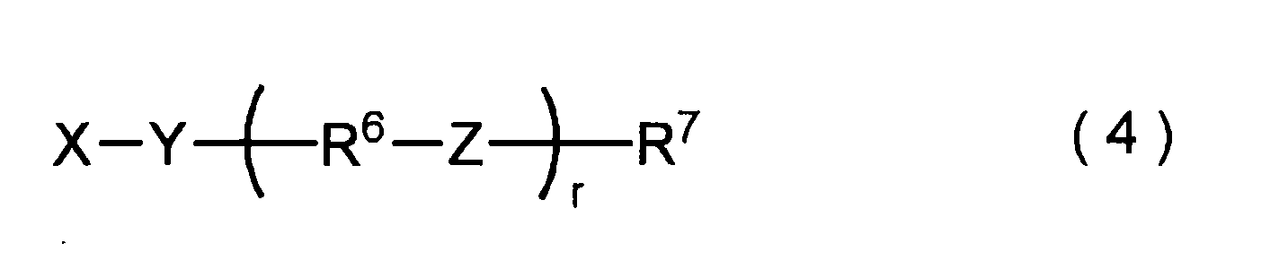
式(4)中、Xは、カルボキシ基、下記式(a)で表わされる基、下記式(b)で表される基、チオール基、ホスホノ基又はアミド基である。Yは、単結合、酸素原子又は硫黄原子である。Zは、エーテル基(酸素原子)、エステル基又はシロキサン基である。R6は、炭素数1~5の2価の鎖状炭化水素基である。R7は、炭素数1~8の1価の鎖状炭化水素基である。rは、自然数である。rが2以上の場合、複数のR6は及びZは、それぞれ同一であっても異なっていてもよい。

式(a)及び(b)中、*は、他部位との結合箇所を示す。
上記Xとしては、カルボキシ基、上記式(a)で表わされる基、上記式(b)で表される基、及びチオール基が好ましく、チオール基がより好ましい。
上記Yとしては、単結合及び硫黄原子が好ましく、単結合が好ましい。また、Xがチオール基、ホスホノ基又はアミド基である場合、Yは単結合であることが好ましい。
上記Zとしては、エーテル基及びエステル基が好ましく、エーテル基がより好ましい。なお、Zがエーテル基である場合、式(1)中の-(R6-Z)r-R7は、ポリオキシアルキレン鎖を形成する。
上記R6で表される炭素数1~5の2価の鎖状炭化水素基としては、メタンジイル基、エタン-1,2-ジイル基、プロパン-1,2-ジイル基、プロパン-1,3-ジイル基、ブタン-1,2-ジイル基、ブタン-1,3-ジイル基等のアルカンジイル基、エテン-1,2-ジイル基等のアルケンジイル基等を挙げることができる。R6としては、炭素数2~4の2価の鎖状炭化水素基が好ましく、炭素数2の2価の鎖状炭化水素基がより好ましい。また、R6は、アルカンジイル基であることも好ましく、エタン-1,2-ジイル基が最も好ましい。
上記R7で表される炭素数1~8の1価の鎖状炭化水素基としては、メチル基、エチル基、プロピル基等のアルキル基、エテニル基、プロペニル基等のアルケニル基、及びエチニル基等のアルキニル基を挙げることができるが、アルキル基が好ましい。また、R7の炭素数は、5以下が好ましく、3以下がより好ましく、1がさらに好ましい。すなわち、R7としては、メチル基が最も好ましい。R7の炭素数が少ない場合、特に極性分散媒中での分散性がより向上する。
上記式(4)におけるrの上限としては、例えば500であり、50が好ましい。上記rの下限は1であるが、2が好ましく、5がより好ましい。
(第2リガンド)
リガンドとしては、上記基xと共に、炭素数6~20の炭化水素基(基z)をさらに有する第2リガンドが用いられていてもよい。基zは特に非極性分散媒に対する良好な分散性を発揮する基であるため、第1リガンドと第2リガンドとを併用することにより、極性分散媒及び非極性分散媒が両存するような分散媒中において、(A)半導体ナノ粒子の分散性がより向上する。また、第2リガンドを用いることで、波長変換膜を形成する際の他の成分との相溶性を高めることもできる。
リガンドとしては、上記基xと共に、炭素数6~20の炭化水素基(基z)をさらに有する第2リガンドが用いられていてもよい。基zは特に非極性分散媒に対する良好な分散性を発揮する基であるため、第1リガンドと第2リガンドとを併用することにより、極性分散媒及び非極性分散媒が両存するような分散媒中において、(A)半導体ナノ粒子の分散性がより向上する。また、第2リガンドを用いることで、波長変換膜を形成する際の他の成分との相溶性を高めることもできる。
第2リガンドの基xは、第1リガンドの基xと同様であり、ナノ結晶の表面に良好に吸着することのできる基である。第2リガンドが有する基xとしては、カルボキシ基及びチオール基が好ましく、チオール基がより好ましい。
基zである炭素数6~20の炭化水素基としては、アルキル基、アルケニル基、アルキニル基、シクロアルキル基等の脂肪族炭化水素基や、フェニル基、ナフチル基等の芳香族炭化水素基を挙げることができるが、脂肪族炭化水素基が好ましく、アルキル基がより好ましい。基zの炭素数の下限としては、8が好ましく、10がより好ましい。一方、この炭素数の上限としては、18が好ましく、16がより好ましい。
第1リガンド及び第2リガンドは、従来公知の方法により、ナノ結晶の表面に配位させることができる。これらのリガンドは、ナノ結晶を合成するときに用られ、ナノ結晶の表面に付着(配位)したリガンドであってもよいし、ナノ結晶を合成した後にリガンド交換によりナノ結晶の表面に配位させたものであってもよい。但し、リガンド交換によっても完全にはリガンドが交換されず、元のリガンドと新しいリガンドとが共存することがある。すなわち、第2リガンドが配位したナノ結晶を合成した後、第1リガンドとのリガンド交換を行った場合、ナノ結晶の表面には、通常第1リガンドと第2リガンドとの両方が配位した状態となる。
第1リガンドと第2リガンドとの合計含有量に対する第1リガンドの含有量の下限は、30質量%が好ましく、50質量%がより好ましく、60質量%がさらに好ましい。また、第1リガンドと第2リガンドとの合計含有量に対する第1リガンドの含有量の上限は、99質量%であってよく、90質量%であってもよい。第1リガンドの含有量が上記範囲内、特に上記下限以上であれば、(D)重合体や(F)分散媒等との親和性が良好になる結果、より良好な蛍光量子収率や分散特性を発揮することができる。また同様に、(A)半導体ナノ粒子が有する全リガンドに占める第1リガンドの含有量も、上記の範囲内であることが好ましい。なお、(A)半導体ナノ粒子中の第1リガンド等のリガンドの含有量は、後述する実施例に記載の方法にて測定することができる。
(A)半導体ナノ粒子の平均粒径の下限としては、0.5nmが好ましく、1.0nmがより好ましい。また、上記平均粒径の上限としては、20nmが好ましく、10nmがより好ましい。平均粒径を上記下限以上とすることで、半導体ナノ粒子の蛍光特性の安定性が高まる。一方、平均粒径を上記上限以下とすることで、量子閉じ込め効果を十分に得ることができ、蛍光特性が向上する。また、平均粒径を上記上限以下とすることで、より良好な分散安定性を発揮することができる。
なお、(A)半導体ナノ粒子の蛍光の波長領域は、ナノ結晶の構成材料や平均粒径を適宜選択することにより制御できる。また、ナノ結晶の形状は特に限定されず、例えば球状、棒状、円盤状、その他の形状であってもよいが、球状及び棒状が好ましい。半導体ナノ粒子が球状であれば、粒子の表面エネルギーが小さくなるため、分散安定性を高めることが出来る。また、半導体ナノ粒子が棒状であれば、偏光発光により光の利用効率を向上させることができる。
当該硬化膜形成用組成物の全固形分に占める(A)半導体ナノ粒子の含有量の下限としては、1質量%が好ましく、5質量%がより好ましく、8質量%がさらに好ましい。(A)半導体ナノ粒子の含有量を上記下限以上とすることで、得られる波長変換膜における発光を十分なものとすることができる。一方、この含有量の上限としては、50質量%が好ましく、30質量%がより好ましく、20質量%がさらに好ましい。(A)半導体ナノ粒子の含有量を上記上限以下とすることで、分散安定性や塗布性をより高めることなどができる。なお、固形分とは、(F)分散媒以外の成分をいう。
((B)ウレタン(メタ)アクリレート)
(B)ウレタン(メタ)アクリレートは、複数の重合性基を有する。ウレタン(メタ)アクリレートとは、ウレタン結合(-NHCOO-)を有する(メタ)アクリレートをいう。ウレタン(メタ)アクリレートは、重合性基として(メタ)アクリロイル基を有するが、エポキシ基、ビニル基等の他の重合性基をさらに有していてもよい。(メタ)アクリロイル基とは、アクリロイル基(-CO-CH=CH2)又はメタクリロイル基(-CO-C(CH3)=CH2)をいい、アクリロイル基であることが好ましい。
(B)ウレタン(メタ)アクリレートは、複数の重合性基を有する。ウレタン(メタ)アクリレートとは、ウレタン結合(-NHCOO-)を有する(メタ)アクリレートをいう。ウレタン(メタ)アクリレートは、重合性基として(メタ)アクリロイル基を有するが、エポキシ基、ビニル基等の他の重合性基をさらに有していてもよい。(メタ)アクリロイル基とは、アクリロイル基(-CO-CH=CH2)又はメタクリロイル基(-CO-C(CH3)=CH2)をいい、アクリロイル基であることが好ましい。
(B)ウレタン(メタ)アクリレートが有する重合性基の数の下限としては、2であってよいが、4が好ましく、6がより好ましく、8がさらに好ましく、9がよりさらに好ましく、10がよりさらに好ましく、12が特に好ましい。一方、この重合性基の数の上限としては、例えば30であり、24が好ましく、18がより好ましい。このような数の重合性基を有する(B)ウレタン(メタ)アクリレートを用いることで、塗布性、分散安定性及び得られる波長変換膜の蛍光性能等がより良好なものとなる。
(B)ウレタン(メタ)アクリレートは、イソシアヌル酸構造、トリアジン構造又はこれらの組み合わせを有することが好ましい。(B)ウレタン(メタ)アクリレートがこのような構造を有する場合、塗布性、分散安定性及び得られる波長変換膜の蛍光性能等がより良好なものとなる。イソシアヌル酸構造としては、下記式(5)で表される構造が挙げられる。トリアジン構造としては、下記式(6)で表される構造が挙げられる。
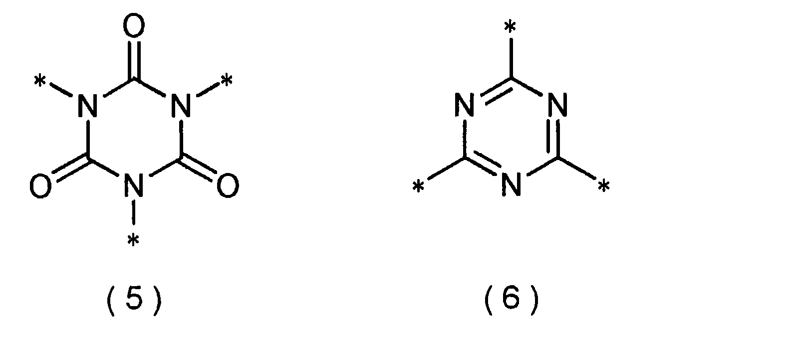
式(5)及び(6)中、*は、他部位との結合箇所を示す。
(B)ウレタン(メタ)アクリレートの分子量の下限としては、例えば300であり、600が好ましく、1,000がより好ましく、1,800がさらに好ましい。一方、この分子量の上限としては、例えば10,000であり、6,000が好ましく、5,000がより好ましく、4,000がさらに好ましい。分子量が上記範囲の(B)ウレタン(メタ)アクリレートを用いることで、塗布性、分散安定性及び得られる波長変換膜の蛍光性能等がより良好なものとなる。(B)ウレタン(メタ)アクリレートが重合体である場合には、重合体の重量平均分子量が上記の数値の範囲内であることが好ましい。重合体の重量平均分子量の測定方法は、実施例に記載したものと同様である。
(B)ウレタン(メタ)アクリレートの好適な形態としては、下記式(1)で表される化合物を挙げることができる。

式(1)中、R1は、炭素数1~60のm価の有機基である。複数のR2は、それぞれ独立して、1又は複数の(メタ)アクリロイル基を含む基である。mは、2又は3である。有機基とは、1以上の炭素原子を含む基をいう。
R1で表される炭素数1~60のm価の有機基としては、m価の炭化水素基、m価の炭化水素基が有する水素原子の一部又は全部を置換基で置換した基、m価の炭化水素基の炭素-炭素間に、CO、CS、O、S、NR’又はこれらのうちの2種以上を組み合わせた基を含む基等が挙げられる。R’は、水素原子又は炭素数1~6の炭化水素基である。上記炭化水素基としては、鎖状炭化水素基、脂環式炭化水素基、芳香族炭化水素基、これらの組み合わせからなる基等が挙げられる。上記置換基としては、ヒドロキシ基、カルボキシ基、アミノ基、シアノ基、ニトロ基、スルホンアミド基等が挙げられる。CO、CS、O、S及びNR’のうちの2種以上を組み合わせた基としては、-COO-、-CONR’-、-NR’COO-等が挙げられる。
R1で表される有機基の炭素数の下限としては、4が好ましく、10がより好ましく、16がさらに好ましい。一方、この炭素数の上限としては、50が好ましく、40がより好ましく、30がさらに好ましい。
mは、3であることが好ましい。
R1で表される炭素数1~60のm価の有機基としては、複素環構造を含む基であることが好ましく、窒素を含む複素環構造を含む基であることがより好ましい。窒素を含む複素環構造としては、トリアジン構造及びイソシアヌル酸構造が挙げられる。R1で表される炭素数1~60のm価の有機基は、窒素を含む複素環構造のみからなる基、及び窒素を含む複素環構造と炭化水素基(より好ましくは鎖状炭化水素基)とからなる基が好ましい。
好適なR1としては、下記式(3-1)及び(3-2)で表される基が挙げられ、特に、式(3-1)で表される基が好ましい。なお、R1が下記式(3-1)又は(3-2)で表されるとき、mは3である。
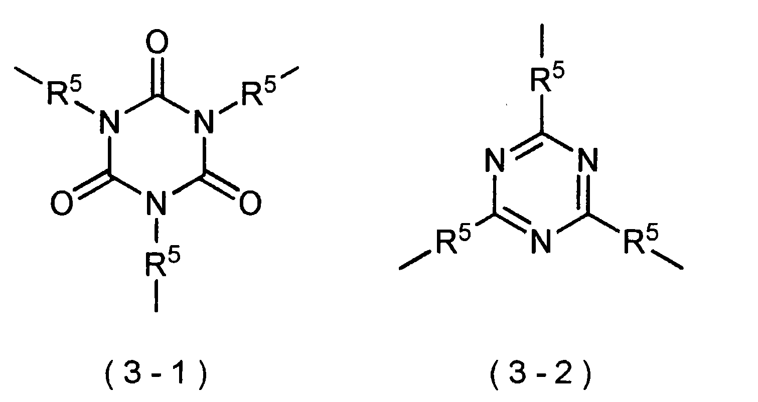
式(3-1)及び(3-2)中、複数のR5は、それぞれ独立して、単結合又は炭素数1~12のアルカンジイル基である。
上記R5としては、アルカンジイル基が好ましい。このアルカンジイル基の炭素数の下限としては、2が好ましく、4がより好ましい。一方、この炭素数の上限としては、10が好ましく、8がより好ましい。このアルカンジイル基は、直鎖状及び分岐鎖状のいずれであってもよいが、直鎖状であることが好ましい。
R2は、1又は複数の(メタ)アクリロイル基を含む基であり、1又は複数の(メタ)アクリロイルオキシ基の数に応じた多価の有機基を介して式(1)におけるウレタン結合に含まれる酸素原子に結合する基であることが好ましい。R2で表される基が有する(メタ)アクリロイル基の数としては特に限定されないが、その下限としては2が好ましく、3がより好ましい。一方、その上限としては10が好ましく、5がより好ましい。
好適なR2としては、下記式(2)で表される基が挙げられる。

式(2)中、R3は、単結合又は炭素数1~3のアルカンジイル基である。R4は、(メタ)アクリロイル基である。nは、1又は2である。pは、0又は1である。qは、1~3の整数である。
R3としては、炭素数1~3のアルカンジイル基が好ましく、メタンジイル基がより好ましい。
R4としては、アクリロイル基が好ましい。
nは、2が好ましい。pは、1が好ましい。qは、3が好ましい。
(B)ウレタン(メタ)アクリレートの市販品としては、新中村化学工業(株)のU-6HA、UA-1100H、U-6LPA、U-15HA、U-6H、U-10HA、U-10PA、UA-53H、UA-33H、根上工業(株)のUN-904、共栄社化学(株)のUA-306H、UA-306T、UA-306I、UA-510H、BASF社のLaromer UA-9048、UA-9050、PR9052、ダイセルオルネクス(株)のEBECRYL 220、5129、8301、KRM8200、8200AE、8452等が挙げられる。
(B)ウレタン(メタ)アクリレートの含有量の下限としては、(A)半導体ナノ粒子100質量部に対して、50質量部が好ましく、100質量部がより好ましく、200質量部がさらに好ましい。(B)ウレタン(メタ)アクリレートの含有量を上記下限以上とすることで、良好な硬化性等を発揮することができる。一方、この含有量の上限としては、1,000質量部が好ましく、500質量部がより好ましく、400質量部がさらに好ましい。(B)ウレタン(メタ)アクリレートの含有量を上記上限以下とすることで、(A)半導体ナノ粒子の含有比率が高まることなどにより、より良好な蛍光性能を発現することなどができる。
((C)光拡散粒子)
(C)光拡散粒子は、光拡散により半導体ナノ粒子に入射される光の量を増加させることにより、蛍光量子収率(波長変換効率)を高める成分である。当該硬化膜形成用組成物が(C)光拡散粒子を含有することで、蛍光量子収率をより高めることなどができる。なお、光拡散粒子は蛍光を発しないという点で半導体ナノ粒子とは異なる。
(C)光拡散粒子は、光拡散により半導体ナノ粒子に入射される光の量を増加させることにより、蛍光量子収率(波長変換効率)を高める成分である。当該硬化膜形成用組成物が(C)光拡散粒子を含有することで、蛍光量子収率をより高めることなどができる。なお、光拡散粒子は蛍光を発しないという点で半導体ナノ粒子とは異なる。
(C)光拡散粒子は、金属酸化物を含むことが好ましく、金属酸化物粒子であることがより好ましい。金属酸化物の中でも、Al2O3、SiO2、ZnO、ZrO2、BaTiO3、TiO2、Ta2O5、Ti3O5、ITO(スズをドープした酸化インジウム)、IZO(亜鉛をドープした酸化インジウム)、ATO(アンチモンをドープした酸化スズ)、AZO(アルミニウムをドープした酸化亜鉛)、Nb2O3、SnO、CeO2、MgO又はこれらの組み合わせが好ましく、酸化チタン(TiO2及びTi3O5)及び酸化セリウム(CeO2)がより好ましい。酸化チタンは励起光を散乱させる能力が優れており、励起光がより量子ドットに入射しやすくなる。
また、(C)光拡散粒子は、酸化チタン(TiO2及びTi3O5)と、この酸化チタンの表面の少なくとも一部を被覆する酸化アルミニウム(Al2O3)とを有する粒子であることが好ましい。酸化チタンは光触媒作用を強く発揮する材料のため、光によって波長変換膜が劣化し、(A)半導体ナノ粒子の波長変換機能を低下させる場合がある。そこで、(C)光拡散粒子が酸化チタンの場合、表面を酸化アルミニウムによって被覆することで光触媒機能を低減させ、良好な蛍光量子収率を得ることができる。
(C)光拡散粒子の平均粒径の下限としては、5nmが好ましく、10nmがより好ましく、30nmがさらに好ましい。(C)光拡散粒子の平均粒径を上記下限以上とすることで、十分な光拡散性を発揮することができる。一方、この平均粒径の上限としては、500nmが好ましく、300nmがより好ましく、250nmがさらに好ましい。(C)光拡散粒子の平均粒径を上記上限以下とすることで、十分な光拡散性、分散性、塗布性等を発揮することができる。
(C)光拡散粒子の含有量の下限としては、(A)半導体ナノ粒子100質量部に対して、10質量部が好ましく、50質量部がより好ましい。(C)光拡散粒子の含有量を上記下限以上とすることで、十分な光拡散性が発揮され、蛍光量子収率を高めることができる。一方、この含有量の上限としては、500質量部が好ましく、300質量部がより好ましく、200質量部がさらに好ましい。(C)光拡散粒子の含有量を上記上限以下とすることで、分散性や塗布性がより向上することなどにより、蛍光量子収率をより高めることができる。
((D)重合体)
(D)重合体は、通常、得られる硬化膜の母材となるバインダー樹脂として機能するものである。なお、(B)ウレタン(メタ)アクリレートは、(D)重合体には含まれない。(D)重合体の一部又は全部は、分散剤として機能するものであってもよい。当該硬化膜形成用組成物が(D)重合体をさらに含むことで、得られる波長変換膜における加熱に伴う(A)半導体ナノ粒子の劣化が抑制され蛍光性能をより高めることなどができる。(D)重合体としては、アクリル樹脂、ポリイミド、ポリシロキサン、芳香族ポリエーテル、ノボラック樹脂等が挙げられ、中でもアクリル樹脂が好ましい。
(D)重合体は、通常、得られる硬化膜の母材となるバインダー樹脂として機能するものである。なお、(B)ウレタン(メタ)アクリレートは、(D)重合体には含まれない。(D)重合体の一部又は全部は、分散剤として機能するものであってもよい。当該硬化膜形成用組成物が(D)重合体をさらに含むことで、得られる波長変換膜における加熱に伴う(A)半導体ナノ粒子の劣化が抑制され蛍光性能をより高めることなどができる。(D)重合体としては、アクリル樹脂、ポリイミド、ポリシロキサン、芳香族ポリエーテル、ノボラック樹脂等が挙げられ、中でもアクリル樹脂が好ましい。
(D)重合体は、酸性基を有することが好ましい。(D)重合体が酸性基を有することにより、分散安定性等が高まり、また、良好なアルカリ可溶性を示す。(D)重合体がアルカリ可溶性である場合、アルカリ現像液などによる良好なパターニングが可能となる。酸性基としては、カルボキシ基、スルホン酸基、リン酸基、フェノール性水酸基等を挙げることができ、カルボキシ基が好ましい。なお、酸性基における水素原子は、金属原子等で置換されていてもよく、解離していてもよい。
(D)重合体は、酸性基を含む側鎖を有することが好ましく、酸性基を含む炭素数5~15の側鎖を有することがより好ましい。側鎖とは、主鎖から分岐した部分である1価の基をいう。(D)重合体がこのような側鎖を有する場合、(A)半導体ナノ粒子との親和性がより良好になる結果、分散性等が特に高まる。上記側鎖の炭素数の下限は、6が好ましく、7がより好ましい。この炭素数の上限は、13がより好ましい。酸性基は、鎖状の側鎖の主鎖側とは反対側の先端に位置していることが好ましい。
酸性基を含む側鎖としては、*-COO-R-COOH(Rは、炭素数3~13の2価の有機基である。*は、主鎖との結合箇所を示す。)で表される基が好ましい。Rとしては、2価の炭化水素基、及びこの炭化水素基の炭素-炭素間に-COO-を含む基が好ましく、2価の炭化水素基の炭素―炭素間に-COO-を含む基がより好ましい。Rには複数の-COO-が含まれていてよい。Rの炭素数の下限としては、4が好ましく、5がより好ましい。Rの炭素数の上限としては、11が好ましい。
(D)重合体は、酸性基を有する構造単位を含むことが好ましく、酸性基を含む側鎖を有する構造単位を含むことがより好ましい。このような構造単位を与える単量体としては、例えばアクリル酸、メタクリル酸、クロトン酸、マレイン酸、フマル酸、シトラコン酸、メサコン酸、イタコン酸、フタル酸モノ[2-(メタ)アクリロイルオキシエチル]、コハク酸モノ(2-アクリロイルオキシエチル)、コハク酸モノ(2-メタクリロイルオキシエチル)、ω-カルボキシ-ポリカプロラクトンモノアクリレート、ヘキサヒドロフタル酸モノ(2-メタクリロイルオキシエチル)等を挙げることができる。これらの中でも、フタル酸モノ[2-(メタ)アクリロイルオキシエチル]、コハク酸モノ(2-アクリロイルオキシエチル)、コハク酸モノ(2-メタクリロイルオキシエチル)、ω-カルボキシ-ポリカプロラクトンモノアクリレート、ヘキサヒドロフタル酸モノ(2-メタクリロイルオキシエチル)等、炭素数5~15の側鎖を与えるものが好ましい。
(D)重合体における酸性基を含む構造単位の含有割合の下限としては、5質量%が好ましく、10質量%がより好ましい。また、この含有割合の上限としては、50質量%が好ましく、40質量%がより好ましく、30質量%が特に好ましい。上記の数値の範囲内であると、アルカリ現像性と分散安定性とに優れる。
(D)重合体は、炭素数4~20の鎖状炭化水素基を有するものが好ましい。(D)重合体が炭素数4~20の鎖状炭化水素基を有することにより、分散安定性及び塗布性が高まり、得られる波長変換膜の蛍光性能もより良好なものとなる。上記鎖状炭化水素基としては、アルキル基が好ましい。また、この鎖状炭化水素基の炭素数の下限としては、6が好ましく、8がより好ましい。一方、この炭素数の上限としては、16が好ましく、12がより好ましい。
(D)重合体は、炭素数4~20の鎖状炭化水素基を有する構造単位を含むことが好ましい。このような構造単位を与える単量体としては、例えばブチル(メタ)アクリレート、ヘキシル(メタ)アクリレート、2-エチルヘキシル(メタ)アクリレート、イソデシル(メタ)アクリレート、ラウリル(メタ)アクリレート、トリデシル(メタ)アクリレート、ステアリル(メタ)アクリレート等の(メタ)アクリル酸アルキルエステルなどが挙げられる。
(D)重合体における炭素数4~20の鎖状炭化水素基を含む構造単位の含有割合の下限としては、5質量%が好ましく、10質量%がより好ましい。また、この含有割合の上限としては、40質量%が好ましく、30質量%がより好ましい。
(D)重合体は、炭素数4~20の鎖状炭化水素基以外の炭化水素基を有する構造単位を含むことが好ましく、環状炭化水素基を有する構造単位を含むことがより好ましい。環状炭化水素基としては、アリール基やシクロアルキル基等が挙げられ、シクロアルキル基が好ましい。炭素数4~20の鎖状炭化水素基以外の炭化水素基の炭素数の下限としては、1であってよいが、2が好ましく、4がより好ましい。また、この炭素数の上限としては、20が好ましく、12がより好ましく、8がさらに好ましい。このような構造単位を与える単量体としては、炭素数1~3のアルキル基を有する(メタ)アクリル酸アルキルエステル、(メタ)アクリル酸シクロアルキルエステル、(メタ)アクリル酸アリールエステル等の(メタ)アクリル酸エステルが挙げられ、(メタ)アクリル酸シクロアルキルエステル及び(メタ)アクリル酸アリールエステルが好ましく、(メタ)アクリル酸シクロアルキルエステルがより好ましい。(メタ)アクリル酸シクロアルキルエステルとしては、シクロヘキシル(メタ)アクリレート、トリシクロ[5.2.1.02,6]デカン-8-イル(メタ)アクリレート、イソボルニル(メタ)アクリレート等が挙げられる。
(D)重合体における炭素数4~20の鎖状炭化水素基以外の炭化水素基を含む構造単位の含有割合の下限としては、10質量%が好ましく、30質量%がより好ましい。また、この含有割合の上限としては、80質量%が好ましく、70質量%がより好ましく、60質量%がさらに好ましい。
また、(D)重合体において、酸性基を含む構造単位、炭素数4~20の鎖状炭化水素基を有する構造単位、及び環状炭化水素基を有する構造単位の合計含有割合の下限が、80質量%であることが好ましいこともあり、90質量%、95質量%、さらには99質量%がより好ましいこともある。
(D)重合体が、酸性基を有する構造単位と、炭素数4~20の鎖状炭化水素基を有する構造単位とを同時に含むものが好ましい。
(D)重合体が、酸性基を有する構造単位と、炭素数4~20の鎖状炭化水素基を有する構造単位とを同時に含むものが好ましい。
(D)重合体は、さらにその他の構造単位を有していてもよい。このような構造単位を与える単量体としては、不飽和ジカルボン酸ジエステル、マレイミド化合物、不飽和芳香族化合物、共役ジエン、テトラヒドロフラン骨格を有する不飽和化合物、その他の不飽和化合物等が挙げられる。
上記各構造単位を有する(D)重合体は、各構造単位を与えるモノマーを公知の方法により重合することにより得ることができる。
(D)重合体の重量平均分子量(Mw)の下限としては、3,000が好ましく、6,000がより好ましく、10,000がさらに好ましい。一方、この重量平均分子量(Mw)の上限としては、50,000が好ましく、30,000がより好ましく、20,000がさらに好ましい。(D)重合体の重量平均分子量(Mw)が上記範囲であることにより、分散安定性や塗布性をより高めることなどができる。
なお、本明細書における重量平均分子量(Mw)の測定方法は、実施例に記載した。
(D)重合体の含有量の下限としては、(A)半導体ナノ粒子100質量部に対して、10質量部が好ましく、100質量部がより好ましく、200質量部がさらに好ましい。一方、この含有量の上限としては、1,000質量部が好ましく、500質量部がより好ましい。(D)重合体の含有量を上記範囲とすることで、分散安定性及び塗布性並びに得られる波長変換膜の蛍光性能をより良好なものとすることができる。
((E)酸化防止剤)
(E)酸化防止剤は、熱や光照射による(A)半導体ナノ粒子、(D)重合体等の酸化劣化を抑制することができる。従って当該硬化膜形成用組成物が(E)酸化防止剤をさらに含有する場合、特に加熱処理等を経て得られる波長変換膜の蛍光量子収率をより高めることができる。
(E)酸化防止剤は、熱や光照射による(A)半導体ナノ粒子、(D)重合体等の酸化劣化を抑制することができる。従って当該硬化膜形成用組成物が(E)酸化防止剤をさらに含有する場合、特に加熱処理等を経て得られる波長変換膜の蛍光量子収率をより高めることができる。
(E)酸化防止剤としては、フェノール系酸化防止剤、リン系酸化防止剤、イオウ系酸化防止剤、ベンゾフェノン系酸化防止剤等を挙げることができる。これらの中でも、フェノール系酸化防止剤が好ましい。フェノール系酸化防止剤を用いることで、加熱処理等を経て得られる波長変換膜の蛍光量子収率をより高めることができる。
フェノール系酸化防止剤としては、例えば2,4,6-トリス(3’,5’-ジ-t-ブチル-4’-ヒドロキシベンジル)メシチレン、2,4-ビス-(n-オクチルチオ)-6-(4-ヒドロキシ-3,5-ジ-t-ブチルアニリノ)-1,3,5-トリアジン、ペンタエリスリトールテトラキス[3-(3,5-ジ-t-ブチル-4-ヒドロキシフェニル)プロピオネート(例えばBASF社の「Irganox1010」)、2,6-ジ-t-ブチル-4-ノニルフェノール、チオジエチレンビス[3-(3,5-ジ-t-ブチル-4-ヒドロキシフェニル)プロピオネート](例えばBASF社の「Irganox1035」)、2,2’-メチレンビス-(6-(1-メチルシクロヘキシル)-p-クレゾール)、N,N-ヘキサメチレンビス(3,5-ジ-t-ブチル-4-ヒドロキシ-ヒドロシンナムアミド)、2,5-ジ-t-ブチルヒドロキノン、2,5-ジ-t-アミル-ヒドロキノン、2,4-ジメチル-6-(1-メチルシクロヘキシル)-フェノール、6-t-ブチル-o-クレゾール、6-t-ブチル-2,4-キシレノール、2,4-ジメチル-6-(1-メチルペンタデシル)フェノール、2,4-ビス(オクチルチオメチル)-o-クレゾール、2,4-ビス(ドデシルチオメチル)-o-クレゾール、エチレンビス(オキシエチレン)ビス[3-(3-t-ブチル-4-ヒドロキシ-5-メチルフェニル)プロピオネート](例えばBASF社の「Irganox245」)、3,9-ビス[2-〔3-(t-ブチル-4-ヒドロキシ-5-メチルフェニル)プロピオニルオキシ〕-1,1-ジメチルエチル]-2,4,8,10-テトラオキサスピロ[5.5]ウンデカン(例えば住友化学社の「スミライザーGA-80」)、トリエチレングリコールビス[3-(3-t-ブチル-4-ヒドロキシ-5-メチルフェニル)プロピオネート(例えばADEKA社の「アデカスタブAO-70」)、2-t-アミルフェノール、2-t-ブチルフェノール、2,4-ジ-t-ブチルフェノール、1,1,3-トリス-(2’-メチル-4’-ヒドロキシ-5’-t-ブチルフェニル)-ブタン、4,4’-ブチリデン-ビス-(2-t-ブチル-5-メチルフェノール)等を挙げることができる。
リン系酸化防止剤としては、例えばトリス(イソデシル)フォスファイト、トリス(トリデシル)フォスファイト、フェニルイソオクチルフォスファイト、フェニルイソデシルフォスファイト、フェニルジ(トリデシル)フォスファイト、ジフェニルイソオクチルフォスファイト、ジフェニルイソデシルフォスファイト、ジフェニルトリデシルフォスファイト、トリフェニルフォスファイト、トリス(ノニルフェニル)フォスファイト、4,4’-イソプロピリデンジフェノールアルキルフォスファイト、トリスノニルフェニルフォスファイト、トリスジノニルフェニルフォスファイト、トリス(2,4-ジ-t-ブチルフェニル)フォスファイト、トリス(ビフェニル)フォスファイト、ジステアリルペンタエリスリトールジフォスファイト、ジ(2,4-ジ-t-ブチルフェニル)ペンタエリスリトールジフォスファイト、ジ(ノニルフェニル)ペンタエリスリトールジフォスファイト、フェニルビスフェノールAペンタエリスリトールジフォスファイト、テトラトリデシル4,4’-ブチリデンビス(3-メチル-6-t-ブチルフェノール)ジフォスファイト、ヘキサトリデシル1,1,3-トリス(2-メチル-4-ヒドロキシ-5-t-ブチルフェニル)ブタントリフォスファイト、3,5-ジ-t-ブチル-4-ヒドロキシベンジルフォスファイトジエチルエステル、1,3-ビス(ジフェノキシフォスフォニロキシ)-ベンゼン、亜リン酸エチルビス(2,4-ジ-t-ブチル-6-メチルフェニル)、トリ-o-トリルホスフィン等を挙げることができる。
(E)酸化防止剤の含有量の下限としては、(A)半導体ナノ粒子100質量部に対して、10質量部が好ましく、30質量部がより好ましい。(E)酸化防止剤の含有量を上記下限以上とすることで、十分な酸化防止性能が発揮され、蛍光量子収率を高めることができる。一方、この含有量の上限としては、200質量部が好ましく、100質量部がより好ましい。(E)酸化防止剤の含有量を上記上限以下とすることで、(A)半導体ナノ粒子の含有比率が高まることなどにより、より良好な蛍光性能を発現することなどができる。
((F)分散媒)
当該硬化膜形成用組成物がさらに(F)分散媒を含有することで、各成分の均一分散性や塗布性が向上する。(F)分散媒としては、極性分散媒及び非極性分散媒を挙げることができるが、分散安定性をより高める観点などから、極性分散媒を含むことが好ましい。
当該硬化膜形成用組成物がさらに(F)分散媒を含有することで、各成分の均一分散性や塗布性が向上する。(F)分散媒としては、極性分散媒及び非極性分散媒を挙げることができるが、分散安定性をより高める観点などから、極性分散媒を含むことが好ましい。
極性分散媒としては、アルコール類、多価アルコールのアルキルエーテル類、多価アルコールのモノアルキルエーテルモノエステル類、ヒドロキシカルボン酸エステル類、カルボン酸類、エーテル類、ケトン類、アミド類、アミン類又はこれらの組み合わせを挙げることができる。
アルコール類としては、例えばメタノール、エタノール、プロパノール、n-ブタノール、n-ペンタノール、n-ヘキサノール、イソプロパノール等のモノアルコール類;エチレングリコール、プロピレングリコール、ジエチレングリコール、ジプロピレングリコール、トリエチレングリコール、トリプロピレングリコール等の多価アルコール類を挙げることができる。
多価アルコールのアルキルエーテル類としては、例えばエチレングリコールモノメチルエーテル、プロピレングリコールモノメチルエーテル、エチレングリコールモノエチルエーテル、プロピレングリコールモノエチルエーテル、エチレングリコールモノプロピルエーテル、プロピレングリコールモノプロピルエーテル、エチレングリコールモノブチルエーテル、プロピレングリコールモノブチルエーテル等の多価アルコールのモノアルキルエーテル類;エチレングリコールジメチルエーテル、プロピレングリコールジメチルエーテル、エチレングリコールジエチルエーテル、プロピレングリコールジエチルエーテル、エチレングリコールジプロピルエーテル、プロピレングリコールジプロピルエーテル、エチレングリコールジブチルエーテル、プロピレングリコールジブチルエーテル等の多価アルコールのポリアルキルエーテル類などを挙げることができる。
多価アルコールのモノアルキルエーテルモノエステル類としては、多価アルコールのモノアルキルエーテルとカルボン酸とのエステルが挙げられ、多価アルコールのモノアルキルエーテルと酢酸とのエステルが好ましい。多価アルコールのモノアルキルエーテルモノエステル類の具体例としては、エチレングリコールモノメチルエーテルアセテート、プロピレングリコールモノメチルエーテルアセテート、エチレングリコールモノエチルエーテルアセテート、プロピレングリコールモノエチルエーテルアセテート、エチレングリコールモノプロピルエーテルアセテート、プロピレングリコールモノプロピルエーテルアセテート、エチレングリコールモノブチルエーテルアセテート、プロピレングリコールモノブチルエーテルアセテート等を挙げることができる。
ヒドロキシカルボン酸エステル類としては、例えばグリコール酸メチル、グリコール酸エチル、乳酸メチル、乳酸エチル、ヒドロキシプロピオン酸メチル、ヒドロキシプロピオン酸エチル、ヒドロキシ酪酸メチル、ヒドロキシ酪酸エチル等を挙げることができる。
カルボン酸類としては、例えばギ酸、酢酸等を挙げることができる。
エーテル類としては、環状又は鎖状のアルキルエーテルなどが挙げられる。エーテル類の具体例としては、例えばテトラヒドロフラン、1,4-ジオキサン、ジメトキシエタン、ジエチルエーテル、ジメチルエーテル等を挙げることができる。
ケトン類としては、例えばアセトン、メチルエチルケトン等を挙げることができる。ケトン類は、置換基を有していてもよく、中でもヒドロキシケトン類が好ましい。ヒドロキシケトン類としては、例えばヒドロキシアセトン、1-ヒドロキシ-2-ブタノン、1-ヒドロキシ-2-ペンタノン、3-ヒドロキシ-2-ブタノン、3-ヒドロキシ-3-ペンタノン等のα-ヒドロキシケトン類;4-ヒドロキシ-2-ブタノン、3-メチル-4-ヒドロキシ-2-ブタノン、ジアセトンアルコール、4-ヒドロキシ-5,5-ジメチル-2-ヘキサノン等のβ-ヒドロキシケトン類;5-ヒドロキシ-2-ペンタノン、5-ヒドロキシ-2-ヘキサノンなどを挙げることができる。
アミド類としては、例えばN,N-ジメチルホルムアミド、N,N-ジメチルアセトアミド等を挙げることできる。
アミン類としては、例えばトリエチルアミン、ピリジン等を挙げることができる。
極性分散媒の中でも、多価アルコールのアルキルエーテル類及び多価アルコールのモノアルキルエーテルモノエステル類が好ましく、多価アルコールのモノアルキルエーテルモノエステル類がより好ましい。
非極性分散媒としては、ベンゼン、トルエン、キシレン、エチルベンゼン等の芳香族炭化水素、ヘキサン、シクロヘキサン等の脂肪族炭化水素などの炭化水素を挙げることができる。
(F)分散媒に占める極性分散媒の含有量の下限としては、30質量%が好ましく、50質量%がより好ましく、70質量%がさらに好ましく、90質量%がさらに好ましい。(F)分散媒に占める極性分散媒の含有量は、実質的に100質量%であってもよい。
(F)分散媒の含有量は特に限定されないが、当該硬化膜形成用組成物に占める(F)分散媒の含有量の下限としては、20質量%が好ましく、30質量%がより好ましい。一方、この含有量の上限としては、90質量%が好ましく、80質量%がより好ましい。(F)分散媒の含有量を上記範囲とすることで、分散安定性、塗布性等をより良好なものとすることができる。
((G)感放射線性化合物)
当該硬化膜形成用組成物は、さらに(G)感放射線性化合物を含有することができる。この場合、当該硬化膜形成用組成物に感放射線性を付与できる。
当該硬化膜形成用組成物は、さらに(G)感放射線性化合物を含有することができる。この場合、当該硬化膜形成用組成物に感放射線性を付与できる。
(G)感放射線性化合物としては、例えば感放射線性ラジカル重合開始剤、感放射線性酸発生剤、感放射線性塩基発生剤、これらの組み合わせ等が挙げられる。これらの中でも、放射線の照射により(B)ウレタン(メタ)アクリレートの硬化反応を促進させることができることから、感放射線性ラジカル重合開始剤を用いることが好ましい。
感放射線性ラジカル重合開始剤の具体例としては、例えばO-アシルオキシム化合物、α-アミノケトン化合物、α-ヒドロキシケトン化合物、アシルホスフィンオキシド化合物等が挙げられる。
O-アシルオキシム化合物としては、例えば1-〔9-エチル-6-(2-メチルベンゾイル)-9.H.-カルバゾール-3-イル〕-エタン-1-オンオキシム-O-アセテート、1-[9-エチル-6-ベンゾイル-9.H.-カルバゾール-3-イル]-オクタン-1-オンオキシム-O-アセテート、1-[9-エチル-6-(2-メチルベンゾイル)-9.H.-カルバゾール-3-イル]-エタン-1-オンオキシム-O-ベンゾエート、1-[9-n-ブチル-6-(2-エチルベンゾイル)-9.H.-カルバゾール-3-イル]-エタン-1-オンオキシム-O-ベンゾエート、エタノン,1-[9-エチル-6-(2-メチル-4-テトラヒドロフラニルベンゾイル)-9.H.-カルバゾール-3-イル]-,1-(O-アセチルオキシム)、エタノン,1-[9-エチル-6-(2-メチル-4-テトラヒドロピラニルベンゾイル)-9.H.-カルバゾール-3-イル]-,1-(O-アセチルオキシム)、エタノン,1-[9-エチル-6-(2-メチル-5-テトラヒドロフラニルベンゾイル)-9.H.-カルバゾール-3-イル]-,1-(O-アセチルオキシム)、エタノン,1-[9-エチル-6-{2-メチル-4-(2,2-ジメチル-1,3-ジオキソラニル)メトキシベンゾイル}-9.H.-カルバゾール-3-イル]-,1-(O-アセチルオキシム)、エタノン,1-[9-エチル-6-(2-メチル-4-テトラヒドロフラニルメトキシベンゾイル)-9.H.-カルバゾール-3-イル]-,1-(O-アセチルオキシム)、1,2-オクタンジオン-1-[4-(フェニルチオ)-2-(O-ベンゾイルオキシム)]、エタノン,1-[9-エチル-6-(2-メチルベンゾイル)-9.H.-カルバゾール-3-イル]-,1-(O-アセチルオキシム)等が挙げられる。
O-アシルオキシム化合物の市販品としては、例えばNCI-831、NCI-930(以上、株式会社ADEKA社製)、DFI-020、DFI-091(以上、ダイトーケミックス株式会社製)イルガキュアOXE01、OXE02、OXE03(以上、BASF社製)等を使用することもできる。
α-アミノケトン化合物としては、例えば2-ベンジル-2-ジメチルアミノ-1-(4-モルホリノフェニル)-ブタン-1-オン、2-ジメチルアミノ-2-(4-メチルベンジル)-1-(4-モルホリン-4-イル-フェニル)-ブタン-1-オン、2-メチル-1-(4-メチルチオフェニル)-2-モルホリノプロパン-1-オン等が挙げられる。
α-ヒドロキシケトン化合物としては、例えば1-フェニル-2-ヒドロキシ-2-メチルプロパン-1-オン、1-(4-i-プロピルフェニル)-2-ヒドロキシ-2-メチルプロパン-1-オン、4-(2-ヒドロキシエトキシ)フェニル-(2-ヒドロキシ-2-プロピル)ケトン、1-ヒドロキシシクロヘキシルフェニルケトン等が挙げられる。
アシルホスフィンオキシド化合物としては、例えば2,4,6-トリメチルベンゾイルジフェニルホスフィンオキシド、ビス(2,4,6-トリメチルベンゾイル)-フェニルホスフィンオキシド等が挙げられる。
感放射線性ラジカル重合開始剤としては、放射線による硬化反応をより促進させる観点から、O-アシルオキシム化合物及びアシルホスフィンオキシド化合物が好ましい。
感放射線性酸発生剤の具体例としては、例えば
ジフェニルヨードニウムトリフルオロメタンスルホネート、ジフェニルヨードニウムピレンスルホネート等のヨードニウム塩系感放射線性酸発生剤;
トリフェニルスルホニウムトリフルオロメタンスルホネート、トリフェニルスルホニウムヘキサフルオロアンチモネート等のスルホニウム塩系感放射線性酸発生剤;
4-ヒドロキシ-1-ナフチルテトラヒドロチオフェニウムトリフルオロメタンスルホネート、4-メトキシ-1-ナフチルテトラヒドロチオフェニウムトリフルオロメタンスルホネート等のテトラヒドロチオフェニウム塩系感放射線性酸発生剤;
トリフルオロメチルスルホニルオキシビシクロ[2.2.1]ヘプト-5-エンジカルボキシイミド、スクシンイミドトリフルオロメチルスルホネート等のイミドスルホネート系感放射線性酸発生剤;
(5-プロピルスルホニルオキシイミノ-5H-チオフェン-2-イリデン)-(2-メチルフェニル)アセトニトリル、(5-オクチルスルホニルオキシイミノ-5H-チオフェン-2-イリデン)-(2-メチルフェニル)アセトニトリル等のオキシムスルホネート系感放射線性酸発生剤;
トリヒドロキシベンゾフェノンの1,2-ナフトキノンジアジドスルホン酸エステル、テトラヒドロキシベンゾフェノンの1,2-ナフトキノンジアジドスルホン酸エステル等のキノンジアジド化合物等が挙げられる。
ジフェニルヨードニウムトリフルオロメタンスルホネート、ジフェニルヨードニウムピレンスルホネート等のヨードニウム塩系感放射線性酸発生剤;
トリフェニルスルホニウムトリフルオロメタンスルホネート、トリフェニルスルホニウムヘキサフルオロアンチモネート等のスルホニウム塩系感放射線性酸発生剤;
4-ヒドロキシ-1-ナフチルテトラヒドロチオフェニウムトリフルオロメタンスルホネート、4-メトキシ-1-ナフチルテトラヒドロチオフェニウムトリフルオロメタンスルホネート等のテトラヒドロチオフェニウム塩系感放射線性酸発生剤;
トリフルオロメチルスルホニルオキシビシクロ[2.2.1]ヘプト-5-エンジカルボキシイミド、スクシンイミドトリフルオロメチルスルホネート等のイミドスルホネート系感放射線性酸発生剤;
(5-プロピルスルホニルオキシイミノ-5H-チオフェン-2-イリデン)-(2-メチルフェニル)アセトニトリル、(5-オクチルスルホニルオキシイミノ-5H-チオフェン-2-イリデン)-(2-メチルフェニル)アセトニトリル等のオキシムスルホネート系感放射線性酸発生剤;
トリヒドロキシベンゾフェノンの1,2-ナフトキノンジアジドスルホン酸エステル、テトラヒドロキシベンゾフェノンの1,2-ナフトキノンジアジドスルホン酸エステル等のキノンジアジド化合物等が挙げられる。
感放射線性塩基発生剤の具体例としては、例えば4-(メチルチオベンゾイル)-1-メチル-1-モルホリノエタン、(4-モルホリノベンゾイル)-1-ベンジル-1-ジメチルアミノプロパン、2-ベンジル-2-ジメチルアミノ-1-(4-モルホリノフェニル)-ブタノン、N-(2-ニトロベンジルオキシカルボニル)ピロリジン、1-(アントラキノン-2-イル)エチルイミダゾールカルボキシレート等の複素環基含有感放射線性塩基発生剤;
2-ニトロベンジルシクロヘキシルカルバメート、[[(2,6-ジニトロベンジル)オキシ]カルボニル]シクロヘキシルアミン、ビス[[(2-ニトロベンジル)オキシ]カルボニル]ヘキサン-1,6-ジアミン、トリフェニルメタノール、o-カルバモイルヒドロキシルアミド、o-カルバモイルオキシム、ヘキサアンミンコバルト(III)トリス(トリフェニルメチルボレート)、1,2-ジシクロヘキシル-4,4,5,5-テトラメチルビグアニジウムn-ブチルトリフェニルボラート等が挙げられる。
2-ニトロベンジルシクロヘキシルカルバメート、[[(2,6-ジニトロベンジル)オキシ]カルボニル]シクロヘキシルアミン、ビス[[(2-ニトロベンジル)オキシ]カルボニル]ヘキサン-1,6-ジアミン、トリフェニルメタノール、o-カルバモイルヒドロキシルアミド、o-カルバモイルオキシム、ヘキサアンミンコバルト(III)トリス(トリフェニルメチルボレート)、1,2-ジシクロヘキシル-4,4,5,5-テトラメチルビグアニジウムn-ブチルトリフェニルボラート等が挙げられる。
(G)感放射線性化合物の含有量の下限としては、(A)半導体ナノ粒子100質量部に対して、1質量部が好ましく、10質量部がより好ましく、30質量部がさらに好ましい。また、上記含有量の上限としては、200質量部が好ましく、100質量部がより好ましい。(G)感放射線性化合物の含有量を上記範囲とすることにより、当該硬化膜形成用組成物の放射線感度や得られる波長変換膜の硬度などをより高めることができる。
(その他の成分)
当該硬化膜形成用組成物は、上述した(A)~(G)成分以外のその他の成分を含有していてもよい。その他の成分としては、熱重合開始剤、接着助剤、保存安定剤、ウレタン(メタ)アクリレート以外の重合性化合物等を挙げることができる。当該硬化膜形成用組成物における上記その他の成分の含有量の上限としては、(A)半導体ナノ粒子100質量部に対して10質量部が好ましいことがあり、1質量部がより好ましいことがある。
当該硬化膜形成用組成物は、上述した(A)~(G)成分以外のその他の成分を含有していてもよい。その他の成分としては、熱重合開始剤、接着助剤、保存安定剤、ウレタン(メタ)アクリレート以外の重合性化合物等を挙げることができる。当該硬化膜形成用組成物における上記その他の成分の含有量の上限としては、(A)半導体ナノ粒子100質量部に対して10質量部が好ましいことがあり、1質量部がより好ましいことがある。
当該硬化膜形成用組成物は、公知の方法により調製することが可能である。当該硬化膜形成用組成物は、例えば(F)分散媒中で、(A)半導体ナノ粒子、(B)ウレタン(メタ)アクリレート及び必要に応じて任意成分を混合することにより調製できる。
<波長変換膜>
本発明の一実施形態に係る波長変換膜は、当該硬化膜形成用組成物から形成される硬化膜である。当該波長変換膜は当該硬化膜形成用組成物から得られるため、蛍光量子収率が高く、その結果例えば高い色再現性を有することができる。当該波長変換膜は、パターン化されていてもよいし、パターン化されていなくてもよいが、当該波長変換膜がパターン化されていると、サブ画素として有用な発光層に適用することができる。当該波長変換膜の形成方法は、特に限定されず、例えば放射線照射により硬化させる方法であっても、加熱により硬化させる方法であってもよい。但し、当該硬化膜形成用組成物を用いているため、加熱により硬化させる方法であっても、蛍光量子収率の高い波長変換膜を得ることができる。当該波長変換膜の具体的な形成方法は後述する。
本発明の一実施形態に係る波長変換膜は、当該硬化膜形成用組成物から形成される硬化膜である。当該波長変換膜は当該硬化膜形成用組成物から得られるため、蛍光量子収率が高く、その結果例えば高い色再現性を有することができる。当該波長変換膜は、パターン化されていてもよいし、パターン化されていなくてもよいが、当該波長変換膜がパターン化されていると、サブ画素として有用な発光層に適用することができる。当該波長変換膜の形成方法は、特に限定されず、例えば放射線照射により硬化させる方法であっても、加熱により硬化させる方法であってもよい。但し、当該硬化膜形成用組成物を用いているため、加熱により硬化させる方法であっても、蛍光量子収率の高い波長変換膜を得ることができる。当該波長変換膜の具体的な形成方法は後述する。
当該波長変換膜は、発光表示素子の発光層としての利用に適している。以下、当該発光表示素子の好適な実施形態について説明する。
<発光表示素子>
図1は、本発明の一実施形態に係る発光表示素子100を模式的に示す断面図である。発光表示素子100は、第1基材12上に発光層13(13a、13b、13c)及びブラックマトリクス14を設けて構成された波長変換基板11と、波長変換基板11上に接着剤層15を介して貼り合わされた光源基板18とを有する。発光層13が、本発明の一実施形態に係る波長変換膜である。
図1は、本発明の一実施形態に係る発光表示素子100を模式的に示す断面図である。発光表示素子100は、第1基材12上に発光層13(13a、13b、13c)及びブラックマトリクス14を設けて構成された波長変換基板11と、波長変換基板11上に接着剤層15を介して貼り合わされた光源基板18とを有する。発光層13が、本発明の一実施形態に係る波長変換膜である。
第1基材12は、透明の基材であり、具体例は後述する。
波長変換基板11の発光層13は、上述した硬化膜形成用組成物を用い、パターニングして形成される。発光層13は、当該硬化膜形成用組成物を用いて形成しているため、半導体ナノ粒子の蛍光量子収率が高く、例えば色再現性の高い発光層とすることができる。
波長変換基板11は、発光層13のそれぞれが含有する半導体ナノ粒子により、光源基板18の光源17からの励起光を波長変換し、所望とする波長の蛍光を発する。波長変換基板11では、第1発光層13aと第2発光層13bと第3発光層13cとが、それぞれ異なる半導体ナノ粒子を含んで構成され、異なる蛍光を発することができる。例えば波長変換基板11は、第1発光層13aが励起光を赤色の光に変換し、第2発光層13bが励起光を緑色の光に変換し、第3発光層13cが励起光を青色の光に変換するように構成することができる。
その場合、各発光層13a、13b、13cは、それぞれが所望とする蛍光特性を有するように、含有する半導体ナノ粒子の選択がなされる。そのため、波長変換基板11の各発光層13a、13b、13cの形成においては、異なる発光特性の半導体ナノ粒子を含む、例えば3種の硬化膜形成用組成物が準備される。
波長変換基板11の発光層13の平均厚さの下限としては、100nmが好ましく、1μmがより好ましい。また、上記平均厚さの上限としては、100μmが好ましい。上記平均厚さを上記下限以上とすることで、励起光を特に十分吸収することができるため、光変換効率が高まり、発光表示素子の輝度を高めることができる。
第1基材12上の各発光層13の間には、ブラックマトリクス14が配置されている。ブラックマトリクス14は、公知の遮光性の材料を用い、公知の方法に従ってパターニングして形成することができる。なお、ブラックマトリクス14は、波長変換基板11において、必須の構成要素ではなく、波長変換基板11は、ブラックマトリクス14を設けない構成とすることも可能である。
接着剤層15は、紫外光又は青色光を透過する公知の接着剤を用いて形成される。なお、接着剤層15は、図1に示すように、第1基材12上に各発光層13の全面を被覆するように設ける必要はなく、波長変換基板11の外縁のみに設けることも可能である。
光源基板18は、第2基材16と、第2基材16の波長変換基板11側に配置された光源17とを備えている。光源17からはそれぞれ励起光として紫外光又は青色光が出射される。
光源17(17a、17b、17c)としては、特に限定されるものではなく、公知の構造の紫外発光有機EL素子、青色発光有機EL素子、紫外発光LED素子、青色発光LED素子等の使用が可能であり、公知の製造方法により作製することが可能である。ここで、紫外光としては、主発光ピークが360nm以上435nm以下であることが好ましく、青色光としては、主発光ピークが435nmを超えて480nm以下であることが好ましい。光源17は、それぞれの出射光が対向する発光層13を照射するように、指向性を有していることが好ましい。
発光表示素子100は、第1光源17aからの励起光を波長変換基板11の第1発光層13aの半導体ナノ粒子により波長変換する。同様に、第2光源17bからの励起光を波長変換基板11の第2発光層13bの半導体ナノ粒子により波長変換し、第3光源17cからの励起光を波長変換基板11の第3発光層13cの半導体ナノ粒子により波長変換する。このようにして、各光源17からの励起光が、それぞれ所望とする波長の可視光に変換されて表示に用いられる。
発光表示素子100においては、第1発光層13aの設けられた部分が、赤色表示を行うサブ画素を構成する。すなわち、波長変換基板11の第1発光層13aは、光源基板18の対向する第1光源17aからの励起光を赤色光に変換する。また、第2発光層13bの設けられた部分が、緑色表示を行うサブ画素を構成する。すなわち、第2発光層13bは、光源基板18の対向する第2光源17bからの励起光を緑色光に変換する。また、第3発光層13cの設けられた部分が、青色表示を行うサブ画素を構成する。例えば励起光として紫外光を用いる場合、第3発光層13cは、光源基板18の対向する第3光源17cからの紫外光を青色光に変換する。図1では第1光源17a、第2光源17b、第3光源17cを分けて図示しているが、基本的には同一光源、特に青色の励起光源であることが好ましく、第1発光層13a、第2発光層13b、第3発光層13cにより各色に変換する実施態様が好ましい。
なお、発光表示素子100においては、第3光源17cからの励起光として青色光を用いる場合、波長変換基板11は、第3発光層13cの代わりに樹脂中に光散乱粒子を分散して構成された光散乱層を用いることも可能である。こうすることで、励起光である青色光を波長変換することなく、そのままの波長特性で使用することができる。
発光表示素子100は、第1発光層13aを備えたサブ画素、第2発光層13bを備えたサブ画素及び第3発光層13cを備えたサブ画素の3種のサブ画素により、画像を構成する最小単位となる1つの画素を構成する。
以上の構成を有する発光表示素子100は、第1発光層13aを備えたサブ画素、第2発光層13bを備えたサブ画素及び第3発光層13cを備えたサブ画素毎に、赤色、緑色又は青色の光の発光が制御され、フルカラーの表示が行われる。
なお、発光表示素子100においては、発光層13と第1基材12との間に、カラーフィルタを設けることが可能である。すなわち、第1発光層13aと第1基材12との間に赤色のカラーフィルタを設け、第2発光層13bと第1基材12との間に緑色のカラーフィルタを設け、第3発光層13cと第1基材12との間に青色のカラーフィルタを設けることができる。これにより、表示の色の純度を高めることができる。ここで、カラーフィルタとしては、表示素子用等として公知のものを公知の方法で形成して用いることができる。
<波長変換膜の形成方法>
本発明の一実施形態に係る波長変換膜の形成方法は、基板上に直接又は間接に塗膜を形成する工程(塗膜形成工程)、及び上記塗膜を加熱する工程(加熱工程)を備え、上記塗膜を当該硬化膜形成用組成物により形成する。当該硬化膜形成用組成物が(G)感放射線性化合物等を含有するときなどは、当該形成方法は、上記塗膜形成工程と加熱工程との間に、上記塗膜の少なくとも一部に放射線を照射(露光)する工程(放射線照射工程)、及び放射線照射後の塗膜を現像する工程(現像工程)をさらに備えていてよい。以下、各工程についてそれぞれ説明する。
本発明の一実施形態に係る波長変換膜の形成方法は、基板上に直接又は間接に塗膜を形成する工程(塗膜形成工程)、及び上記塗膜を加熱する工程(加熱工程)を備え、上記塗膜を当該硬化膜形成用組成物により形成する。当該硬化膜形成用組成物が(G)感放射線性化合物等を含有するときなどは、当該形成方法は、上記塗膜形成工程と加熱工程との間に、上記塗膜の少なくとも一部に放射線を照射(露光)する工程(放射線照射工程)、及び放射線照射後の塗膜を現像する工程(現像工程)をさらに備えていてよい。以下、各工程についてそれぞれ説明する。
(塗膜形成工程)
塗膜形成工程では、例えば当該硬化膜形成用組成物を基板上に直接又は間接に塗布することにより塗膜を形成する。当該硬化膜形成用組成物を塗布後、塗布面を加熱(プレベーク)することにより溶媒等を除去してもよい。
塗膜形成工程では、例えば当該硬化膜形成用組成物を基板上に直接又は間接に塗布することにより塗膜を形成する。当該硬化膜形成用組成物を塗布後、塗布面を加熱(プレベーク)することにより溶媒等を除去してもよい。
塗膜を形成する基板の材質としては、特に限定されるものではないが、例えばガラス、石英、シリコン、樹脂等が挙げられる。上記樹脂の具体例としては、例えばポリエチレンテレフタレート、ポリエチレンナフタレート、ポリブチレンテレフタレート、ポリエーテルスルホン、ポリカーボネート、ポリイミド、環状オレフィンの付加重合体、環状オレフィンの開環重合体、その水素添加物等が挙げられる。また、これらの基板には、所望により、シランカップリング剤等による薬剤処理、プラズマ処理、イオンプレーティング、スパッタリング、真空蒸着等の前処理を施しておいてもよい。
当該硬化膜形成用組成物の塗布方法としては特に限定されず、例えばスプレー法、ロールコート法、回転塗布法(スピンコート法)、スリットダイ塗布法、バー塗布法等の方法を採用することができる。これらの塗布方法の中でも、スピンコート法及びスリットダイ塗布法が好ましい。加熱(プレベーク)の条件は、各成分の種類、配合割合等によっても異なるが、例えば70℃以上130℃以下、好ましくは100℃以下の温度で、1分以上10分以下の加熱時間とすればよい。
(放射線照射工程)
放射線照射工程では、基板上に形成された塗膜の少なくとも一部に放射線を照射する。塗膜の一部にのみ放射線を照射する際には、例えば所望の形状のパターンを有するフォトマスクを介して放射線を照射してもよい。このフォトマスクを用いることにより、照射された放射線の一部がフォトマスクを通過し、その一部の放射線が塗膜に照射される。
放射線照射工程では、基板上に形成された塗膜の少なくとも一部に放射線を照射する。塗膜の一部にのみ放射線を照射する際には、例えば所望の形状のパターンを有するフォトマスクを介して放射線を照射してもよい。このフォトマスクを用いることにより、照射された放射線の一部がフォトマスクを通過し、その一部の放射線が塗膜に照射される。
照射に使用される放射線としては、可視光線、紫外線、遠紫外線、電子線、X線等が挙げられる。これらの放射線の中でも、波長が190nm以上450nm以下の範囲にある放射線が好ましく、365nmの紫外線を含む放射線がより好ましい。
放射線照射工程における積算照射量(露光量)の下限としては、100J/m2が好ましく、200J/m2がより好ましい。また、上記積算照射量の上限としては、2,000J/m2が好ましく、1,000J/m2がより好ましい。なお、本明細書において「積算照射量」とは、放射線の波長365nmにおける強度を照度計(例えばOAI Optical Associates Inc.社の「OAI model 356」)により測定した値の積算値をいう。
(現像工程)
現像工程では、放射線照射後の塗膜を現像して不要な部分を除去する。現像に使用される現像液としては、例えば水酸化ナトリウム、水酸化カリウム、炭酸ナトリウム、ケイ酸ナトリウム、メタケイ酸ナトリウム、アンモニア、テトラメチルアンモニウムヒドロキシド、テトラエチルアンモニウムヒドロキシド等のアルカリ性化合物の少なくとも1種を溶解した水溶液を使用することができる。上述のアルカリ性化合物の水溶液には、メタノール、エタノール等の水溶性有機溶媒を適当量添加して使用することもできる。
現像工程では、放射線照射後の塗膜を現像して不要な部分を除去する。現像に使用される現像液としては、例えば水酸化ナトリウム、水酸化カリウム、炭酸ナトリウム、ケイ酸ナトリウム、メタケイ酸ナトリウム、アンモニア、テトラメチルアンモニウムヒドロキシド、テトラエチルアンモニウムヒドロキシド等のアルカリ性化合物の少なくとも1種を溶解した水溶液を使用することができる。上述のアルカリ性化合物の水溶液には、メタノール、エタノール等の水溶性有機溶媒を適当量添加して使用することもできる。
現像方法としては、例えば液盛り法、ディッピング法、揺動浸漬法、スプレー法等が挙げられる。現像時間は、硬化膜形成用組成物の組成によって異なるが、その現像時間の下限としては、5秒が好ましく、10秒がより好ましい。また、現像時間の上限としては、300秒が好ましく、180秒がより好ましい。現像処理に続いて、例えば流水洗浄を30秒以上90秒以下の時間で行った後、圧縮空気や圧縮窒素で乾燥させることにより、所望のパターンが得られる。
(加熱工程)
加熱工程では、塗膜を、ホットプレート、オーブン等の適当な加熱装置により加熱する(ポストベーク)。これにより基板上に十分な硬化がされた波長変換膜が得られる。
加熱工程では、塗膜を、ホットプレート、オーブン等の適当な加熱装置により加熱する(ポストベーク)。これにより基板上に十分な硬化がされた波長変換膜が得られる。
本工程の加熱温度の下限としては100℃が好ましく、140℃がより好ましい。加熱温度を上記下限以上とすることで、より十分な硬化を行うことができる。また、上記加熱温度の上限としては250℃が好ましく、220℃がより好ましい。加熱温度を上記上限以下とすることで、半導体ナノ粒子等の劣化を抑え、得られる波長変換膜の蛍光量子収率をより高めることができる。加熱をホットプレートで行う場合、加熱時間の下限としては、5分が好ましく、上限としては30分が好ましい。また、加熱をオーブン中で行う場合、加熱時間の下限としては10分が好ましく、上限としては180分が好ましい。
上述した発光表示素子100の発光層の形成に上記方法を適用する場合は、3種の硬化膜形成用組成物をそれぞれ用いて、上述した工程を含む発光層の形成方法を繰り返して、第1発光層13a、第2発光層13b及び第3発光層13cをそれぞれ形成すればよい。なお、実施例において具体例を示してはいないが、本発明の硬化膜形成用組成物は、インクジェット用の組成物として使用することもできる。
以下、本発明を実施例に基づいて具体的に説明するが、本発明はこれらの実施例に限定されるものではない。
[重量平均分子量(Mw)及び数平均分子量(Mn)]
下記条件によるゲルパーミエーションクロマトグラフィー(GPC)によりMw及びMnを測定した。
装置:昭和電工社の「GPC-101」
カラム:昭和電工社の「GPC-KF-801」、「GPC-KF-802」、「GPC-KF-803」及び「GPC-KF-804」を連結したもの
移動相:テトラヒドロフラン
カラム温度:40℃
流速:1.0mL/分
試料濃度:1.0質量%
試料注入量:100μL
検出器:示差屈折計
標準物質:単分散ポリスチレン
下記条件によるゲルパーミエーションクロマトグラフィー(GPC)によりMw及びMnを測定した。
装置:昭和電工社の「GPC-101」
カラム:昭和電工社の「GPC-KF-801」、「GPC-KF-802」、「GPC-KF-803」及び「GPC-KF-804」を連結したもの
移動相:テトラヒドロフラン
カラム温度:40℃
流速:1.0mL/分
試料濃度:1.0質量%
試料注入量:100μL
検出器:示差屈折計
標準物質:単分散ポリスチレン
[合成例1]半導体ナノ粒子(A-1)の合成
(In(OLA)3溶液(溶液A)の調製)
真空ライン及び窒素ラインへの連結管、熱電対温度計並びにセプタムを3つの口に取り付け、攪拌子を入れた3つ口フラスコを用意した。この3つ口フラスコ中で、酢酸インジウム(In(OAc)3)0.57g、オレイン酸(OLA)1.66g及びオクタデセン(ODE)7.52gを混合した。この後、混合物を減圧下、260℃まで加熱し、260℃で1時間保持し、副生する酢酸、水及び酸素を除いた。これにより、溶液Aを得た。
(In(OLA)3溶液(溶液A)の調製)
真空ライン及び窒素ラインへの連結管、熱電対温度計並びにセプタムを3つの口に取り付け、攪拌子を入れた3つ口フラスコを用意した。この3つ口フラスコ中で、酢酸インジウム(In(OAc)3)0.57g、オレイン酸(OLA)1.66g及びオクタデセン(ODE)7.52gを混合した。この後、混合物を減圧下、260℃まで加熱し、260℃で1時間保持し、副生する酢酸、水及び酸素を除いた。これにより、溶液Aを得た。
(P(SiMe3)3・オクタデセン溶液(溶液B)の調製)
グローブボックス中でトリス(トリメチルシリル)ホスフィン(P(SiMe3)3)0.25g及びODE0.98gを混合し、得られた溶液Bを耐圧バイアルに封入した。
グローブボックス中でトリス(トリメチルシリル)ホスフィン(P(SiMe3)3)0.25g及びODE0.98gを混合し、得られた溶液Bを耐圧バイアルに封入した。
(InPコアの合成)
上記調製した溶液Aを300℃に加熱し、別途調製し脱気した、亜鉛ミリスチン酸塩の20質量%ODE溶液を添加した。その後、上記調製した溶液Bをキャニュラにより迅速に溶液Aが入ったフラスコに圧送した。圧送後、反応液温度は265℃に低下したので、反応温度を270℃にし、2時間反応を進行させた。その後、反応液を室温まで冷却した。なお、In(OLA)3、P(SiMe3)3、及びコア合成の際のリガンドとなる亜鉛ミリスチン酸塩が、それぞれ2mmol、1mmol及び3mmolのモル数となるように、溶液A、溶液B及び亜鉛ミリスチン酸塩を用いた。
上記調製した溶液Aを300℃に加熱し、別途調製し脱気した、亜鉛ミリスチン酸塩の20質量%ODE溶液を添加した。その後、上記調製した溶液Bをキャニュラにより迅速に溶液Aが入ったフラスコに圧送した。圧送後、反応液温度は265℃に低下したので、反応温度を270℃にし、2時間反応を進行させた。その後、反応液を室温まで冷却した。なお、In(OLA)3、P(SiMe3)3、及びコア合成の際のリガンドとなる亜鉛ミリスチン酸塩が、それぞれ2mmol、1mmol及び3mmolのモル数となるように、溶液A、溶液B及び亜鉛ミリスチン酸塩を用いた。
(コア分散液の調製)
上記反応液の入ったフラスコをグローブボックス中に移し、内容液をビーカーに移した。反応液が入ったビーカーにトルエン8gを加えた後、n-ブタノール100gを加え、粒子を沈降させた。その後、遠心分離を行ってから粒子を沈降分離させた。沈降した粒子から上澄み溶媒を除き、粒子を再びトルエン20gに分散させた。同様の操作を5回繰り返し行った。その後、再分散液にn-ブタノール100gを加え、粒子を再度沈降させ、真空乾燥(50℃、1.0Torr、1時間)により粒子を乾燥させた。本乾燥粒子にヘキサン10gを加え再分散させ、InPコアのヘキサン分散液を得た。
上記反応液の入ったフラスコをグローブボックス中に移し、内容液をビーカーに移した。反応液が入ったビーカーにトルエン8gを加えた後、n-ブタノール100gを加え、粒子を沈降させた。その後、遠心分離を行ってから粒子を沈降分離させた。沈降した粒子から上澄み溶媒を除き、粒子を再びトルエン20gに分散させた。同様の操作を5回繰り返し行った。その後、再分散液にn-ブタノール100gを加え、粒子を再度沈降させ、真空乾燥(50℃、1.0Torr、1時間)により粒子を乾燥させた。本乾燥粒子にヘキサン10gを加え再分散させ、InPコアのヘキサン分散液を得た。
(ZnSシェルの合成)
得られたコア分散液から、InPコアが100mg含有する量のコア分散液を取り出した。取り出したコア分散液をZn(OLA)23.75mmol/ODE5g溶液と混合した後、真空下60℃で1時間加熱し、ヘキサンを十分に取り除いた。なお、Zn(OLA)2とドデカンチオールとの反応により、ZnSシェルが形成される。フラスコの中を窒素で戻し、窒素雰囲気にした。その後、この溶液を200℃まで加熱し、30分間同温度で維持し、InPコアをZnSシェルが被覆したコアシェル型のナノ結晶からなる半導体ナノ粒子(A-1)を得た。
得られたコア分散液から、InPコアが100mg含有する量のコア分散液を取り出した。取り出したコア分散液をZn(OLA)23.75mmol/ODE5g溶液と混合した後、真空下60℃で1時間加熱し、ヘキサンを十分に取り除いた。なお、Zn(OLA)2とドデカンチオールとの反応により、ZnSシェルが形成される。フラスコの中を窒素で戻し、窒素雰囲気にした。その後、この溶液を200℃まで加熱し、30分間同温度で維持し、InPコアをZnSシェルが被覆したコアシェル型のナノ結晶からなる半導体ナノ粒子(A-1)を得た。
[合成例2]半導体ナノ粒子(A-2)の合成
(リガンド添加)
上記合成例1で得られたコアシェル型のナノ結晶からなる半導体ナノ粒子(A-1)を含む反応液を210℃に加熱し、ドデカンチオール3.75mmol/ODE5g溶液を30分かけて添加し、その後1.5時間同温度で維持した。さらに、Zn(OLA)3/ODE溶液を添加した後、ドデカンチオールをシリンジポンプより適当な時間かけて混合溶液に添加することにより、半導体ナノ粒子(A-2)を合成した。なお、最後に添加したドデカンチオールが、リガンド(第2リガンド)としてZnSシェルの外面に付着することとなる。すなわち、得られたこの半導体ナノ粒子(A-2)は、InPコアにZnSシェルが被覆したコアシェル型のナノ結晶と、リガンドとしてこのナノ結晶に付着するドデカンチオールとを有する。
(リガンド添加)
上記合成例1で得られたコアシェル型のナノ結晶からなる半導体ナノ粒子(A-1)を含む反応液を210℃に加熱し、ドデカンチオール3.75mmol/ODE5g溶液を30分かけて添加し、その後1.5時間同温度で維持した。さらに、Zn(OLA)3/ODE溶液を添加した後、ドデカンチオールをシリンジポンプより適当な時間かけて混合溶液に添加することにより、半導体ナノ粒子(A-2)を合成した。なお、最後に添加したドデカンチオールが、リガンド(第2リガンド)としてZnSシェルの外面に付着することとなる。すなわち、得られたこの半導体ナノ粒子(A-2)は、InPコアにZnSシェルが被覆したコアシェル型のナノ結晶と、リガンドとしてこのナノ結晶に付着するドデカンチオールとを有する。
合成された半導体ナノ粒子(A-2)を含む反応液が入ったビーカー中でトルエン10gを加えた後、n-ブタノール150gを加え、粒子を沈降させ遠心分離により粒子を分離した。沈降した粒子から上澄み溶媒を除き、粒子を再びトルエン20gに分散した。その後、分散液にn-ブタノール1100gを加え、粒子を沈降させ遠心分離により粒子を分離した。同様の操作を5回行った後、粒子を真空乾燥(50℃、133Pa、1時間)により乾燥させた。
(平均粒径の測定)
得られた半導体ナノ粒子(A-2)について、透過型電子顕微鏡(日本電子社の「JEM-2010F」)を用いて平均粒径を測定した。具体的には、任意に選択した20個の粒子の長径及び短径をそれぞれ測定し、各粒子の直径((長径+短径)/2)を求め、平均値を算出した。半導体ナノ粒子(A-2)の平均粒径は、4.8nmであった。
得られた半導体ナノ粒子(A-2)について、透過型電子顕微鏡(日本電子社の「JEM-2010F」)を用いて平均粒径を測定した。具体的には、任意に選択した20個の粒子の長径及び短径をそれぞれ測定し、各粒子の直径((長径+短径)/2)を求め、平均値を算出した。半導体ナノ粒子(A-2)の平均粒径は、4.8nmであった。
(シェル被覆状況の判定)
上記半導体ナノ粒子(A-2)のTEM測定のEDS(エネルギー分散型X線分析)を用いた元素マッピングにより、ZnSのみを含む粒子がコアシェルナノ結晶100個あたり1個未満であることを確認した。これより、実質的に全てのZn及びSが、In及びPを含むコアシェルナノ結晶を被覆していることを確認した。
上記半導体ナノ粒子(A-2)のTEM測定のEDS(エネルギー分散型X線分析)を用いた元素マッピングにより、ZnSのみを含む粒子がコアシェルナノ結晶100個あたり1個未満であることを確認した。これより、実質的に全てのZn及びSが、In及びPを含むコアシェルナノ結晶を被覆していることを確認した。
[合成例3]半導体ナノ粒子(A-3)の合成
(リガンド交換)
100mgの上記合成例2で得られた半導体ナノ粒子(A-2)を含むトルエン分散液を調製した。この分散液に、リガンドとなる下記式で表されるポリエチレングリコールメチルエーテルチオールを加え70℃で1時間加熱した。その後、洗浄、乾燥を繰り返し、半導体ナノ粒子(A-3)の分散液を得た。半導体ナノ粒子(A-3)は、半導体ナノ粒子(A-2)のリガンドのドデカンチオールの一部が、ポリエチレングリコールメチルエーテルチオールに交換されたものである。半導体ナノ粒子(A-3)の第1リガンドと第2リガンドの含有量を核磁気共鳴装置にて測定(BRUKER社製AVANCEIII HDを用い、CDCl3にサンプルの固形分濃度が2質量%になるように半導体ナノ粒子を溶解させ、1H NMR測定の標準シークエンスにより測定)したところ、第1リガンドと第2リガンドの合計含有量に対する第1リガンドの含有量は40質量%であった。
(リガンド交換)
100mgの上記合成例2で得られた半導体ナノ粒子(A-2)を含むトルエン分散液を調製した。この分散液に、リガンドとなる下記式で表されるポリエチレングリコールメチルエーテルチオールを加え70℃で1時間加熱した。その後、洗浄、乾燥を繰り返し、半導体ナノ粒子(A-3)の分散液を得た。半導体ナノ粒子(A-3)は、半導体ナノ粒子(A-2)のリガンドのドデカンチオールの一部が、ポリエチレングリコールメチルエーテルチオールに交換されたものである。半導体ナノ粒子(A-3)の第1リガンドと第2リガンドの含有量を核磁気共鳴装置にて測定(BRUKER社製AVANCEIII HDを用い、CDCl3にサンプルの固形分濃度が2質量%になるように半導体ナノ粒子を溶解させ、1H NMR測定の標準シークエンスにより測定)したところ、第1リガンドと第2リガンドの合計含有量に対する第1リガンドの含有量は40質量%であった。
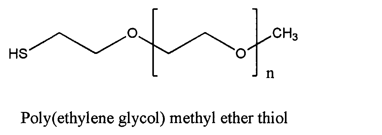
[合成例4]半導体ナノ粒子(A-4)の合成
上記合成例3で記載のリガンド交換のうち、ポリエチレングリコールメチルエーテルチオールを加え70℃で1時間加熱する工程と、n-ブタノール12gを加え、粒子を沈降させ遠心分離により粒子を分離する工程とを2回繰り返して行ったこと以外は、合成例3と同様の操作を行った。これにより、第1リガンドと第2リガンドの合計量に対する第1リガンドの含有量が60質量%である半導体ナノ粒子(A-4)を得た。
上記合成例3で記載のリガンド交換のうち、ポリエチレングリコールメチルエーテルチオールを加え70℃で1時間加熱する工程と、n-ブタノール12gを加え、粒子を沈降させ遠心分離により粒子を分離する工程とを2回繰り返して行ったこと以外は、合成例3と同様の操作を行った。これにより、第1リガンドと第2リガンドの合計量に対する第1リガンドの含有量が60質量%である半導体ナノ粒子(A-4)を得た。
[合成例5]重合体(D-1)の合成
攪拌機を備えたフラスコに、プロピレングリコールモノメチルエーテルアセテート200質量部、シクロヘキシルメタクリレート70質量部、コハク酸モノ(2-メタクリロイルオキシエチル)20質量部、メタクリル酸10質量部、2,2’-アゾビスイソブチロニトリル3.0質量部、及びペンタエリスリトールテトラキス(3-メルカプトプロピオネート)7.0質量部を仕込んで窒素置換した。混合溶液を80℃にて保持して4時間重合した。その後、反応溶液の温度を100℃に昇温させ、さらに1時間重合した後、室温に冷却した。これにより、シクロヘキシルメタクリレートとコハク酸モノ(2-メタクリロイルアクリレート)とメタクリル酸の共重合体(D-1)のプロピレングリコールモノメチルエーテルアセテート溶液を得た。得られた重合体(D-1)のMwは13,500、Mnは7,100であった。なお、合成例5~8において、得られた重合体における各構造単位の含有割合は、対応する単量体の仕込量の比率と同じとみなすことができる。
攪拌機を備えたフラスコに、プロピレングリコールモノメチルエーテルアセテート200質量部、シクロヘキシルメタクリレート70質量部、コハク酸モノ(2-メタクリロイルオキシエチル)20質量部、メタクリル酸10質量部、2,2’-アゾビスイソブチロニトリル3.0質量部、及びペンタエリスリトールテトラキス(3-メルカプトプロピオネート)7.0質量部を仕込んで窒素置換した。混合溶液を80℃にて保持して4時間重合した。その後、反応溶液の温度を100℃に昇温させ、さらに1時間重合した後、室温に冷却した。これにより、シクロヘキシルメタクリレートとコハク酸モノ(2-メタクリロイルアクリレート)とメタクリル酸の共重合体(D-1)のプロピレングリコールモノメチルエーテルアセテート溶液を得た。得られた重合体(D-1)のMwは13,500、Mnは7,100であった。なお、合成例5~8において、得られた重合体における各構造単位の含有割合は、対応する単量体の仕込量の比率と同じとみなすことができる。
[合成例6]重合体(D-2)の合成
合成例5のコハク酸モノ(2-メタクリロイルオキシエチル)20質量部を2-エチルヘキシルメタクリレート20質量部とした以外は、合成例5と同様にして重合体(D-2)のプロピレングリコールモノメチルエーテルアセテート溶液を得た。得られた重合体(D-2)のMwは13,300、Mnは7,000であった。
合成例5のコハク酸モノ(2-メタクリロイルオキシエチル)20質量部を2-エチルヘキシルメタクリレート20質量部とした以外は、合成例5と同様にして重合体(D-2)のプロピレングリコールモノメチルエーテルアセテート溶液を得た。得られた重合体(D-2)のMwは13,300、Mnは7,000であった。
[合成例7]重合体(D-3)の合成
合成例5のシクロヘキシルメタクリレートの仕込量を50質量部にし、さらに2-エチルヘキシルメタクリレート20質量部を仕込んだ以外は、合成例5と同様にして重合体(D-3)のプロピレングリコールモノメチルエーテルアセテート溶液を得た。得られた重合体(D-3)のMwは13,700、Mnは7,100であった。
合成例5のシクロヘキシルメタクリレートの仕込量を50質量部にし、さらに2-エチルヘキシルメタクリレート20質量部を仕込んだ以外は、合成例5と同様にして重合体(D-3)のプロピレングリコールモノメチルエーテルアセテート溶液を得た。得られた重合体(D-3)のMwは13,700、Mnは7,100であった。
[合成例8]重合体(D-4)の合成
合成例5のシクロヘキシルメタクリレートの仕込量を94質量部、コハク酸モノ(2-メタクリロイルオキシエチル)4質量部、メタクリル酸2質量部とした以外は、合成例5と同様にして重合体(D-4)のプロピレングリコールモノメチルエーテルアセテート溶液を得た。得られた重合体(D-4)のMwは13,600、Mnは7,100であった。
合成例5のシクロヘキシルメタクリレートの仕込量を94質量部、コハク酸モノ(2-メタクリロイルオキシエチル)4質量部、メタクリル酸2質量部とした以外は、合成例5と同様にして重合体(D-4)のプロピレングリコールモノメチルエーテルアセテート溶液を得た。得られた重合体(D-4)のMwは13,600、Mnは7,100であった。
以下に実施例及び比較例で用いた各成分を示す。
(A)半導体ナノ粒子
・A-2:上記合成例2で得られた半導体ナノ粒子(A-2)
・A-3:上記合成例3で得られた半導体ナノ粒子(A-3)
・A-4:上記合成例4で得られた半導体ナノ粒子(A-4)
(A)半導体ナノ粒子
・A-2:上記合成例2で得られた半導体ナノ粒子(A-2)
・A-3:上記合成例3で得られた半導体ナノ粒子(A-3)
・A-4:上記合成例4で得られた半導体ナノ粒子(A-4)
(B)ウレタン(メタ)アクリレート及びその他の(メタ)アクリレート
・B-1:ウレタン(メタ)アクリレート(イソシアヌル酸構造及びウレタン結合を有し、重合性基数が15であり、分子量が約2300である下記式で表されるウレタンアクリレート 新中村化学社製の「U-15HA」)
・B-1:ウレタン(メタ)アクリレート(イソシアヌル酸構造及びウレタン結合を有し、重合性基数が15であり、分子量が約2300である下記式で表されるウレタンアクリレート 新中村化学社製の「U-15HA」)

・B-2:ウレタン(メタ)アクリレート(ウレタン結合を有し、イソシアヌル酸構造又はトリアジン構造を有さず、重合性基数が10であり、分子量が約4900であるウレタンアクリレート 根上工業社製の「UN-904」)
・B-3:ウレタン(メタ)アクリレート(ウレタン構造を有し、重合性基数が9であり、分子量が約1400であるウレタンアクリレート 新中村化学社製の「UA-33H」)
・B-4:ウレタン(メタ)アクリレート(ウレタン構造を有し、重合性基数が6であり、分子量が約760である下記式で表されるウレタンアクリレート 新中村化学社製の「U-6LPA」)

B-5:ウレタン(メタ)アクリレート(トリアジン構造及びウレタン結合を有し、重合性基数が6であり、分子量が約1019である下記式で表されるウレタンアクリレート)
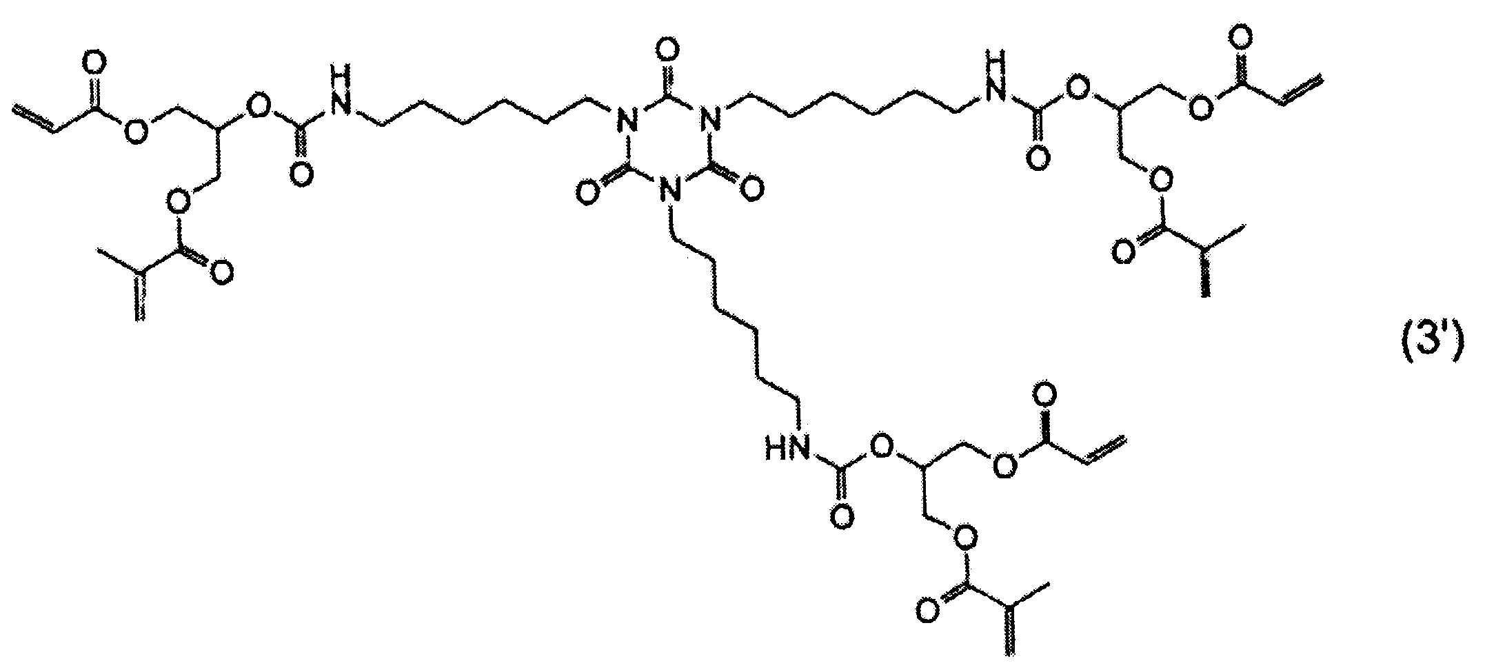
・b-1:ジペンタエリスリトールヘキサアクリレート
(C)光拡散粒子
・C-1:酸化アルミニウムでコーティングされた酸化チタン粒子(平均粒径150nm、 堺化学社の「A-190」)
・C-2:酸化セリウム粒子(平均粒径60nm SOLVAY社の「ZENUS HC60」)
・C-1:酸化アルミニウムでコーティングされた酸化チタン粒子(平均粒径150nm、 堺化学社の「A-190」)
・C-2:酸化セリウム粒子(平均粒径60nm SOLVAY社の「ZENUS HC60」)
(D)重合体
・D-1:上記合成例5で得られた重合体(D-1)
・D-2:上記合成例6で得られた重合体(D-2)
・D-3:上記合成例7で得られた重合体(D-3)
・D-4:上記合成例8で得られた重合体(D-4)
・D-1:上記合成例5で得られた重合体(D-1)
・D-2:上記合成例6で得られた重合体(D-2)
・D-3:上記合成例7で得られた重合体(D-3)
・D-4:上記合成例8で得られた重合体(D-4)
(E)酸化防止剤
・E-1:フェノール系酸化防止剤(3,9-ビス[2-〔3-(t-ブチル-4-ヒドロキシ-5-メチルフェニル)プロピオニルオキシ〕-1,1-ジメチルエチル]-2,4,8,10-テトラオキサスピロ[5.5]ウンデカン(住友化学社の「スミライザーGA-80」)
・E-1:フェノール系酸化防止剤(3,9-ビス[2-〔3-(t-ブチル-4-ヒドロキシ-5-メチルフェニル)プロピオニルオキシ〕-1,1-ジメチルエチル]-2,4,8,10-テトラオキサスピロ[5.5]ウンデカン(住友化学社の「スミライザーGA-80」)
(F)分散媒
・F-1:プロピレングリコールモノメチルエーテルアセテート
・F-2:トルエン
・F-1:プロピレングリコールモノメチルエーテルアセテート
・F-2:トルエン
(G)感放射線性化合物
・G-1:2,2-ジメトキシ-1,2--ジフェニルエタン-1-オン(IGM Resins B.V.社の「Omnirad651」)と2-メチル-1-[4-(メチルチオ)フェニル]-2-モルフォリノプロパン-1-オン(IGM Resins B.V.社の「Omnirad907」)との質量比1:1の混合物
・G-2:2,4,6-トリメチルベンゾイルジフェニルホスフィンオキシド(IGM Resins B.V.社の「ルシリンLR8953X」)とO-アシルオキシム化合物(ADEKA社の「NCI-930」)との質量比1:1の混合物
・G-3:ビス(2,4,6-トリメチルベンゾイル)-フェニルフォスフィンオキサイド(IGM Resins B.V.社の「Omnirad819」)とエタノン,1-[9-エチル-6-(2-メチルベンゾイル)-9H-カルバゾール-3-イル]-,1-(O-アセチルオキシム)(BASF社の「Irgacure OXE02」)との質量比1:1の混合物
・G-1:2,2-ジメトキシ-1,2--ジフェニルエタン-1-オン(IGM Resins B.V.社の「Omnirad651」)と2-メチル-1-[4-(メチルチオ)フェニル]-2-モルフォリノプロパン-1-オン(IGM Resins B.V.社の「Omnirad907」)との質量比1:1の混合物
・G-2:2,4,6-トリメチルベンゾイルジフェニルホスフィンオキシド(IGM Resins B.V.社の「ルシリンLR8953X」)とO-アシルオキシム化合物(ADEKA社の「NCI-930」)との質量比1:1の混合物
・G-3:ビス(2,4,6-トリメチルベンゾイル)-フェニルフォスフィンオキサイド(IGM Resins B.V.社の「Omnirad819」)とエタノン,1-[9-エチル-6-(2-メチルベンゾイル)-9H-カルバゾール-3-イル]-,1-(O-アセチルオキシム)(BASF社の「Irgacure OXE02」)との質量比1:1の混合物
[実施例1]
分散媒(F-1)100質量部に、半導体ナノ粒子(A-4)10質量部、ウレタン(メタ)アクリレート(B-1)30質量部、光拡散粒子(C-1)10質量部、酸化防止剤(E-1)5質量部、及び感放射線性化合物(G-1)5質量部を加え、実施例1の硬化膜形成用組成物を調製した。
分散媒(F-1)100質量部に、半導体ナノ粒子(A-4)10質量部、ウレタン(メタ)アクリレート(B-1)30質量部、光拡散粒子(C-1)10質量部、酸化防止剤(E-1)5質量部、及び感放射線性化合物(G-1)5質量部を加え、実施例1の硬化膜形成用組成物を調製した。
[実施例2~16、及び比較例1、2]
各配合成分の種類及び配合量を下記表1に記載の通りとしたこと以外は、実施例1と同様にして各硬化膜形成用組成物を調製した。
各配合成分の種類及び配合量を下記表1に記載の通りとしたこと以外は、実施例1と同様にして各硬化膜形成用組成物を調製した。
得られた各硬化膜形成用組成物について、下記の方法に従い評価した。
[蛍光量子収率]
蛍光量子収率は、下記形成方法により得られた波長変換膜について、絶対PL蛍光量子収率測定装置(浜松ホトニクス社の「C11347-01」)を用いて、25℃において測定した。励起光の波長は450nmとした。また、別途、下記形成方法により得られた波長変換膜をクリーンオーブンにて180℃、20分の加熱処理(ポストベーク)を行った後に、上記と同様の方法で蛍光量子収率を測定した。前者の蛍光量子収率(未処理)及び後者の蛍光量子収率(熱処理後)について、以下の基準にて評価した。
・蛍光量子収率(未処理)
AA:60%以上
A :55%以上60%未満
B :50%以上55%未満
C :50%未満
・蛍光量子収率(熱処理後)
AA:55%以上
A :50%以上55%未満
B :40%以上50%未満
C :40%未満
AA、A及びBの場合、蛍光量子収率が高く、蛍光性能が良好であると判断した。評価結果を表1に示す。
蛍光量子収率は、下記形成方法により得られた波長変換膜について、絶対PL蛍光量子収率測定装置(浜松ホトニクス社の「C11347-01」)を用いて、25℃において測定した。励起光の波長は450nmとした。また、別途、下記形成方法により得られた波長変換膜をクリーンオーブンにて180℃、20分の加熱処理(ポストベーク)を行った後に、上記と同様の方法で蛍光量子収率を測定した。前者の蛍光量子収率(未処理)及び後者の蛍光量子収率(熱処理後)について、以下の基準にて評価した。
・蛍光量子収率(未処理)
AA:60%以上
A :55%以上60%未満
B :50%以上55%未満
C :50%未満
・蛍光量子収率(熱処理後)
AA:55%以上
A :50%以上55%未満
B :40%以上50%未満
C :40%未満
AA、A及びBの場合、蛍光量子収率が高く、蛍光性能が良好であると判断した。評価結果を表1に示す。
(波長変換膜の形成方法)
無アルカリガラス基板上に、各硬化膜形成用組成物をスピンナにより塗布した後、90℃のホットプレート上で2分間プレベークすることにより塗膜を形成した。次に、得られた塗膜に、フォトマスクを介さずに、高圧水銀ランプを用いて365nm、405nm及び436nmの各波長を含む放射線を700J/m2の積算照射量で照射することにより、平均厚さ5μmの波長変換膜を形成した。
無アルカリガラス基板上に、各硬化膜形成用組成物をスピンナにより塗布した後、90℃のホットプレート上で2分間プレベークすることにより塗膜を形成した。次に、得られた塗膜に、フォトマスクを介さずに、高圧水銀ランプを用いて365nm、405nm及び436nmの各波長を含む放射線を700J/m2の積算照射量で照射することにより、平均厚さ5μmの波長変換膜を形成した。
[半値幅]
上記方法にて得られた波長変換膜(加熱処理後)について、絶対PL蛍光量子収率測定装置(浜松ホトニクス社の「C11347-01」)を用いて、25℃において蛍光半値幅を測定した。励起光の波長は450nmとした。半値幅は、その値が小さいほど加熱処理後においても色純度の高い蛍光に波長変換できているため良いことを示す。半値幅について、以下の基準で評価した。
AA:45nm未満
A :45nm以上50nm未満
B :50nm以上55nm未満
C :55nm以上
AA、A及びBの場合、半値幅が十分に狭く、蛍光性能が良好であると判断した。評価結果を表1に示す。
上記方法にて得られた波長変換膜(加熱処理後)について、絶対PL蛍光量子収率測定装置(浜松ホトニクス社の「C11347-01」)を用いて、25℃において蛍光半値幅を測定した。励起光の波長は450nmとした。半値幅は、その値が小さいほど加熱処理後においても色純度の高い蛍光に波長変換できているため良いことを示す。半値幅について、以下の基準で評価した。
AA:45nm未満
A :45nm以上50nm未満
B :50nm以上55nm未満
C :55nm以上
AA、A及びBの場合、半値幅が十分に狭く、蛍光性能が良好であると判断した。評価結果を表1に示す。
[塗布性]
上記波長変換膜(加熱処理後)の表面の算術平均表面粗さ(Ra)を、触針式段差計(商品名「Alpha-Step IQ surface Profiler ASIQ」、KLA-tencor社製)を用いて測定し、以下の基準にて評価した。
A:Ra 500オングストローム未満
B:Ra 500オングストローム以上1000オングストローム未満
C:Ra 1000オングストローム以上
A及びBの場合、塗布性が良好であると判断した。評価結果を表1に示す。
上記波長変換膜(加熱処理後)の表面の算術平均表面粗さ(Ra)を、触針式段差計(商品名「Alpha-Step IQ surface Profiler ASIQ」、KLA-tencor社製)を用いて測定し、以下の基準にて評価した。
A:Ra 500オングストローム未満
B:Ra 500オングストローム以上1000オングストローム未満
C:Ra 1000オングストローム以上
A及びBの場合、塗布性が良好であると判断した。評価結果を表1に示す。
[分散安定性]
各硬化膜形成用組成物を調製後、攪拌機を用い10分攪拌し、2時間経過後の沈降の様子を確認し、以下の基準にて評価した。
AA:沈降が見られなかった
A :殆ど沈降がなかった
B :沈降が一部見られた
C :沈降が多く見られた
AA、A及びBの場合、分散安定性が良好であると判断した。評価結果を表1に示す。
各硬化膜形成用組成物を調製後、攪拌機を用い10分攪拌し、2時間経過後の沈降の様子を確認し、以下の基準にて評価した。
AA:沈降が見られなかった
A :殆ど沈降がなかった
B :沈降が一部見られた
C :沈降が多く見られた
AA、A及びBの場合、分散安定性が良好であると判断した。評価結果を表1に示す。

表1に示されるように、重合性化合物としてウレタン(メタ)アクリレートを用いた実施例1~16の硬化膜形成用組成物は、得られる波長変換膜の蛍光性能(蛍光量子収率及び半値幅)が良好であり、分散安定性及び塗布性も良好であることがわかる。一方、ウレタン(メタ)アクリレートを含まない比較例1、2の硬化膜形成用組成物は、得られる波長変換膜の蛍光性能、分散安定性及び塗布性の全てが良好な結果にはならなかった。
本発明の硬化膜形成用組成物は、発光表示素子の波長変換膜等の形成材料として好適に用いることができる。
11 波長変換基板
12 第1基材
13 発光層(波長変換膜)
13a 第1発光層
13b 第2発光層
13c 第3発光層
14 ブラックマトリクス
15 接着剤層
16 第2基材
17 光源
17a 第1光源
17b 第2光源
17c 第3光源
18 光源基板
100 発光表示素子
12 第1基材
13 発光層(波長変換膜)
13a 第1発光層
13b 第2発光層
13c 第3発光層
14 ブラックマトリクス
15 接着剤層
16 第2基材
17 光源
17a 第1光源
17b 第2光源
17c 第3光源
18 光源基板
100 発光表示素子
Claims (18)
- (A)半導体ナノ粒子、及び
(B)複数の重合性基を有するウレタン(メタ)アクリレート
を含有する硬化膜形成用組成物。 - 上記(B)ウレタン(メタ)アクリレートが、4以上30以下の(メタ)アクリレート基を有する請求項1に記載の硬化膜形成用組成物。
- 上記(A)半導体ナノ粒子がリガンドを有し、
上記リガンドが、カルボキシ基、チオール基、ホスホノ基、アミド基又はこれらの組み合わせを有する請求項1又は請求項2に記載の硬化膜形成用組成物。 - 上記(B)ウレタン(メタ)アクリレートが、イソシアヌル酸構造、トリアジン構造又はこれらの組み合わせを有する請求項1、請求項2又は請求項3に記載の硬化膜形成用組成物。
- 上記(B)ウレタン(メタ)アクリレートの分子量が、600以上6,000以下である請求項1から請求項4のいずれか1項に記載の硬化膜形成用組成物。
- 上記(B)ウレタン(メタ)アクリレートが、下記式(1)で表される請求項1から請求項5のいずれか1項に記載の硬化膜形成用組成物。

(式(1)中、R1は、炭素数1~60のm価の有機基である。複数のR2は、それぞれ独立して、1又は複数の(メタ)アクリロイル基を含む基である。mは、2又は3である。) - 上記式(1)中のR2が、下記式(2)で表される請求項6に記載の硬化膜形成用組成物。

(式(2)中、R3は、単結合又は炭素数1~3のアルカンジイル基である。R4は、(メタ)アクリロイル基である。nは、1又は2である。pは、0又は1である。qは、1~3の整数である。) - 上記式(1)中のR1が下記式(3-1)又は(3-2)で表され、mが3である請求項6又は請求項7に記載の硬化膜形成用組成物。

(式(3-1)及び(3-2)中、複数のR5は、それぞれ独立して、単結合又は炭素数1~12のアルカンジイル基である。) - (C)光拡散粒子
をさらに含有する請求項1から請求項8のいずれか1項に記載の硬化膜形成用組成物。 - (D)重合体
をさらに含有する請求項1から請求項9のいずれか1項に記載の硬化膜形成用組成物。 - 上記(D)重合体が、酸性基を有する請求項10に記載の硬化膜形成用組成物。
- 上記(D)重合体が、酸性基を有する構造単位を5質量%以上含む、請求項10又は請求項11に記載の硬化膜形成用組成物。
- 上記(D)重合体が、上記酸性基を含む炭素数5~15の側鎖を有する請求項11又は請求項12に記載の硬化膜形成用組成物。
- 上記(D)重合体が、炭素数4~20の鎖状炭化水素基を有する請求項10から請求項13のいずれか1項に記載の硬化膜形成用組成物。
- 上記(D)重合体が、酸性基を有する構造単位と、炭素数4~20の鎖状炭化水素基を有する構造単位とを同時に含む、請求項10に記載の硬化膜形成用組成物。
- 請求項1から請求項15のいずれか1項に記載の硬化膜形成用組成物から形成される波長変換膜。
- 請求項16に記載の波長変換膜を備える発光表示素子。
- 基板上に直接又は間接に塗膜を形成する工程、及び
上記塗膜を加熱する工程
を備え、
上記塗膜を請求項1から請求項15のいずれか1項に記載の硬化膜形成用組成物により形成する波長変換膜の形成方法。
Applications Claiming Priority (2)
| Application Number | Priority Date | Filing Date | Title |
|---|---|---|---|
| JP2019-070724 | 2019-04-02 | ||
| JP2019070724A JP2022084963A (ja) | 2019-04-02 | 2019-04-02 | 硬化膜形成用組成物、波長変換膜、発光表示素子、及び波長変換膜の形成方法 |
Publications (1)
| Publication Number | Publication Date |
|---|---|
| WO2020204073A1 true WO2020204073A1 (ja) | 2020-10-08 |
Family
ID=72667910
Family Applications (1)
| Application Number | Title | Priority Date | Filing Date |
|---|---|---|---|
| PCT/JP2020/015031 Ceased WO2020204073A1 (ja) | 2019-04-02 | 2020-04-01 | 硬化膜形成用組成物、波長変換膜、発光表示素子、及び波長変換膜の形成方法 |
Country Status (3)
| Country | Link |
|---|---|
| JP (1) | JP2022084963A (ja) |
| TW (1) | TW202104535A (ja) |
| WO (1) | WO2020204073A1 (ja) |
Cited By (2)
| Publication number | Priority date | Publication date | Assignee | Title |
|---|---|---|---|---|
| WO2023163516A1 (ko) * | 2022-02-23 | 2023-08-31 | 삼성디스플레이 주식회사 | 경화성 조성물, 이를 이용한 막 및 디스플레이 장치 |
| WO2024043110A1 (ja) * | 2022-08-22 | 2024-02-29 | 富士フイルム株式会社 | 感光性組成物、膜および光センサ |
Families Citing this family (2)
| Publication number | Priority date | Publication date | Assignee | Title |
|---|---|---|---|---|
| CN114628566B (zh) * | 2022-03-28 | 2023-06-09 | 东莞市中麒光电技术有限公司 | 光色转换结构、发光单元及发光单元制作方法 |
| TW202526507A (zh) * | 2023-08-30 | 2025-07-01 | 日商日產化學股份有限公司 | 圖型形成用組成物及其用途 |
Citations (5)
| Publication number | Priority date | Publication date | Assignee | Title |
|---|---|---|---|---|
| JPH05272096A (ja) * | 1992-03-25 | 1993-10-19 | Mitsubishi Paper Mills Ltd | 蓄光発光性シート及びその製造方法 |
| JP2009536679A (ja) * | 2006-05-10 | 2009-10-15 | スリーエム イノベイティブ プロパティズ カンパニー | 蛍光無機ナノ粒子を含有する組成物及びコーティング |
| JP2015028139A (ja) * | 2013-06-24 | 2015-02-12 | Jsr株式会社 | 硬化性樹脂組成物、硬化膜、発光素子、波長変換フィルムおよび発光層の形成方法 |
| JP2017032918A (ja) * | 2015-08-05 | 2017-02-09 | Jsr株式会社 | 硬化膜形成用組成物、硬化膜、発光表示素子、フィルム及び硬化膜の形成方法 |
| WO2017086362A1 (ja) * | 2015-11-20 | 2017-05-26 | Jsr株式会社 | ナノ粒子集合体及びその製造方法、ナノ粒子集合体組成物、波長変換層、並びにリガンド |
-
2019
- 2019-04-02 JP JP2019070724A patent/JP2022084963A/ja active Pending
-
2020
- 2020-04-01 TW TW109111221A patent/TW202104535A/zh unknown
- 2020-04-01 WO PCT/JP2020/015031 patent/WO2020204073A1/ja not_active Ceased
Patent Citations (5)
| Publication number | Priority date | Publication date | Assignee | Title |
|---|---|---|---|---|
| JPH05272096A (ja) * | 1992-03-25 | 1993-10-19 | Mitsubishi Paper Mills Ltd | 蓄光発光性シート及びその製造方法 |
| JP2009536679A (ja) * | 2006-05-10 | 2009-10-15 | スリーエム イノベイティブ プロパティズ カンパニー | 蛍光無機ナノ粒子を含有する組成物及びコーティング |
| JP2015028139A (ja) * | 2013-06-24 | 2015-02-12 | Jsr株式会社 | 硬化性樹脂組成物、硬化膜、発光素子、波長変換フィルムおよび発光層の形成方法 |
| JP2017032918A (ja) * | 2015-08-05 | 2017-02-09 | Jsr株式会社 | 硬化膜形成用組成物、硬化膜、発光表示素子、フィルム及び硬化膜の形成方法 |
| WO2017086362A1 (ja) * | 2015-11-20 | 2017-05-26 | Jsr株式会社 | ナノ粒子集合体及びその製造方法、ナノ粒子集合体組成物、波長変換層、並びにリガンド |
Cited By (3)
| Publication number | Priority date | Publication date | Assignee | Title |
|---|---|---|---|---|
| WO2023163516A1 (ko) * | 2022-02-23 | 2023-08-31 | 삼성디스플레이 주식회사 | 경화성 조성물, 이를 이용한 막 및 디스플레이 장치 |
| WO2024043110A1 (ja) * | 2022-08-22 | 2024-02-29 | 富士フイルム株式会社 | 感光性組成物、膜および光センサ |
| EP4579342A4 (en) * | 2022-08-22 | 2026-01-14 | Fujifilm Corp | PHOTOSENSITIVE COMPOSITION, FILM AND OPTICAL SENSOR |
Also Published As
| Publication number | Publication date |
|---|---|
| TW202104535A (zh) | 2021-02-01 |
| JP2022084963A (ja) | 2022-06-08 |
Similar Documents
| Publication | Publication Date | Title |
|---|---|---|
| TWI824082B (zh) | 量子點、量子點分散體、量子點光轉換組合物、自發光感光性樹脂組合物、量子點發光二極體、量子點膜、濾色器、光轉換層疊基材及影像顯示裝置 | |
| KR102638805B1 (ko) | 감광성 조성물 및 색 변환 필름 | |
| WO2019167751A1 (ja) | 半導体ナノ粒子含有組成物、波長変換膜、発光表示素子、及び波長変換膜の形成方法 | |
| JP7482810B2 (ja) | 光変換硬化性組成物、量子ドット発光ダイオード、量子ドットフィルム、前記組成物を用いて形成される硬化膜および前記硬化膜を含む画像表示装置 | |
| JP7008699B2 (ja) | 自発光感光性樹脂組成物、これを利用して製造されたカラーフィルターおよび画像表示装置 | |
| JP6171923B2 (ja) | 硬化性樹脂組成物、硬化膜、発光素子、波長変換フィルムおよび発光層の形成方法 | |
| JP6834213B2 (ja) | 樹脂組成物、膜、波長変換部材、及び膜の形成方法 | |
| KR102116971B1 (ko) | 감광성 수지 조성물 및 표시장치 | |
| WO2006103908A1 (ja) | 半導体ナノクリスタル用有機配位子 | |
| TWI708828B (zh) | 感光性圖案形成用材料 | |
| TWI742244B (zh) | 彩色濾光片及影像顯示裝置 | |
| JP6754499B2 (ja) | 自発光感光性樹脂組成物、これを利用して製造されたカラーフィルターおよび画像表示装置 | |
| KR20180063188A (ko) | 감광성 조성물 및 색 변환 필름 | |
| TW202104535A (zh) | 硬化膜形成用組成物、波長轉換膜、發光顯示元件及波長轉換膜的形成方法 | |
| KR102520299B1 (ko) | 감광성 조성물, 색 변환 매체, 광학 디바이스 및 그의 제조 방법 | |
| JP2023107228A (ja) | 量子ドット、量子ドット分散液、光変換硬化性組成物、前記組成物を用いて形成される硬化膜および前記硬化膜を含む画像表示装置 | |
| KR20230113051A (ko) | 양자점, 양자점 분산액, 광변환 경화성 조성물, 상기 조성물을 이용하여 형성되는 경화막 및 상기 경화막을 포함하는 화상표시장치 | |
| JP2021033093A (ja) | 半導体ナノ粒子含有組成物、波長変換膜及び発光表示素子 | |
| KR20190108710A (ko) | 황색 경화성 수지 조성물, 이를 포함하는 컬러필터 및 화상표시장치 | |
| TWI908138B (zh) | 可固化組成物、使用所述組成物的固化層及包括所述固化層的顯示裝置 | |
| TWI924393B (zh) | 可固化組成物、使用該組成物的固化層、包括固化層的彩色濾光片、及包括彩色濾光片的顯示裝置 | |
| JP7487134B2 (ja) | 光変換インク組成物、カラーフィルタ、及び画像表示装置 | |
| TWI916866B (zh) | 可固化組成物、使用所述組成物的固化層及包括所述固化層的顯示裝置 | |
| TW202535986A (zh) | 可固化組成物、使用該組成物的固化層、包括固化層的彩色濾光片、及包括彩色濾光片的顯示裝置 | |
| TW202336208A (zh) | 量子點、量子點分散液、光轉換固化性組合物、使用該組合物形成的固化膜及圖像顯示裝置 |
Legal Events
| Date | Code | Title | Description |
|---|---|---|---|
| 121 | Ep: the epo has been informed by wipo that ep was designated in this application |
Ref document number: 20783999 Country of ref document: EP Kind code of ref document: A1 |
|
| NENP | Non-entry into the national phase |
Ref country code: DE |
|
| 122 | Ep: pct application non-entry in european phase |
Ref document number: 20783999 Country of ref document: EP Kind code of ref document: A1 |
|
| NENP | Non-entry into the national phase |
Ref country code: JP |