WO2020203036A1 - 光検出装置および電子機器 - Google Patents
光検出装置および電子機器 Download PDFInfo
- Publication number
- WO2020203036A1 WO2020203036A1 PCT/JP2020/009644 JP2020009644W WO2020203036A1 WO 2020203036 A1 WO2020203036 A1 WO 2020203036A1 JP 2020009644 W JP2020009644 W JP 2020009644W WO 2020203036 A1 WO2020203036 A1 WO 2020203036A1
- Authority
- WO
- WIPO (PCT)
- Prior art keywords
- transistor
- power supply
- gate
- drain
- voltage
- Prior art date
- Legal status (The legal status is an assumption and is not a legal conclusion. Google has not performed a legal analysis and makes no representation as to the accuracy of the status listed.)
- Ceased
Links
Images















Classifications
-
- H—ELECTRICITY
- H04—ELECTRIC COMMUNICATION TECHNIQUE
- H04N—PICTORIAL COMMUNICATION, e.g. TELEVISION
- H04N25/00—Circuitry of solid-state image sensors [SSIS]; Control thereof
- H04N25/70—SSIS architectures; Circuits associated therewith
- H04N25/76—Addressed sensors, e.g. MOS or CMOS sensors
-
- H—ELECTRICITY
- H04—ELECTRIC COMMUNICATION TECHNIQUE
- H04N—PICTORIAL COMMUNICATION, e.g. TELEVISION
- H04N25/00—Circuitry of solid-state image sensors [SSIS]; Control thereof
- H04N25/70—SSIS architectures; Circuits associated therewith
- H04N25/71—Charge-coupled device [CCD] sensors; Charge-transfer registers specially adapted for CCD sensors
- H04N25/75—Circuitry for providing, modifying or processing image signals from the pixel array
-
- H—ELECTRICITY
- H04—ELECTRIC COMMUNICATION TECHNIQUE
- H04N—PICTORIAL COMMUNICATION, e.g. TELEVISION
- H04N25/00—Circuitry of solid-state image sensors [SSIS]; Control thereof
- H04N25/70—SSIS architectures; Circuits associated therewith
- H04N25/76—Addressed sensors, e.g. MOS or CMOS sensors
- H04N25/77—Pixel circuitry, e.g. memories, A/D converters, pixel amplifiers, shared circuits or shared components
- H04N25/772—Pixel circuitry, e.g. memories, A/D converters, pixel amplifiers, shared circuits or shared components comprising A/D, V/T, V/F, I/T or I/F converters
-
- H—ELECTRICITY
- H04—ELECTRIC COMMUNICATION TECHNIQUE
- H04N—PICTORIAL COMMUNICATION, e.g. TELEVISION
- H04N25/00—Circuitry of solid-state image sensors [SSIS]; Control thereof
- H04N25/70—SSIS architectures; Circuits associated therewith
- H04N25/76—Addressed sensors, e.g. MOS or CMOS sensors
- H04N25/78—Readout circuits for addressed sensors, e.g. output amplifiers or A/D converters
Definitions
- the present disclosure relates to a photodetector capable of detecting light and an electronic device provided with such a photodetector.
- Patent Document 1 discloses an imaging device that performs AD conversion based on a signal having a lamp waveform and a pixel signal.
- the photodetector includes a first pixel, a reference signal generation unit, and a first comparison unit.
- the first pixel is configured to be capable of generating a first pixel signal.
- the reference signal generation unit is configured to be able to generate a reference signal.
- the first comparison unit can generate a first power supply voltage based on the power supply voltage and the bias voltage supplied from the first power supply node, and can output the first power supply voltage from the output terminal. It has a circuit and a first comparison circuit that can operate based on a first power supply voltage and can perform a comparison operation based on a first pixel signal and a reference signal.
- the electronic device is provided with the above-mentioned photodetector, and corresponds to, for example, a smartphone, a digital camera, a video camera, a notebook personal computer, or the like.
- the first pixel generates the first pixel signal
- the reference signal generation unit generates the reference signal.
- the first power supply circuit generates a first power supply voltage based on the power supply voltage and the bias voltage supplied from the first power supply node. Then, the comparison operation is performed based on the first pixel signal and the first signal by the first comparison circuit that can operate based on the first power supply voltage.
- FIG. 1 shows a configuration example of an image pickup apparatus 1 to which the photodetector according to the embodiment is applied.
- the image pickup apparatus 1 includes a pixel array 11, a drive unit 12, a reference signal generation unit 13, a reading unit 20, a signal processing unit 14, and an image pickup control unit 15.
- the pixel array 11 has a plurality of pixels P arranged in a matrix.
- the pixel P is configured to generate a pixel voltage Vpix according to the amount of light received.
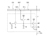
- FIG. 2 shows an example of one configuration of pixel P.
- the pixel array 11 has a plurality of control lines TGL, a plurality of control lines RSTL, a plurality of control line SELLs, and a plurality of signal lines VSL.
- the control line TGL extends in the horizontal direction (horizontal direction in FIG. 2), and one end thereof is connected to the drive unit 12.
- a control signal STG is supplied to the control line TGL by the drive unit 12.
- the control line RSTL extends in the horizontal direction, and one end thereof is connected to the drive unit 12.
- a control signal SRST is supplied to the control line RSTL by the drive unit 12.
- the control line SELL extends in the horizontal direction, and one end thereof is connected to the drive unit 12.
- a control signal SSEL is supplied to the control line SELL by the drive unit 12.
- the signal line VSL extends in the vertical direction (vertical direction in FIG. 2), and one end thereof is connected to the reading unit 20.
- This signal line VSL transmits the signal SIG generated by the pixel P to the reading unit 20.
- Pixel P has a photodiode PD, a transistor TG, a floating diffusion FD, and transistors RST, AMP, and SEL.
- the transistors TG, RST, AMP, and SEL are N-type MOS (Metal Oxide Semiconductor) transistors in this example.
- the photodiode PD is a photoelectric conversion element that generates an amount of electric charge according to the amount of light received and stores the generated electric charge inside.
- the anode of the photodiode PD is grounded and the cathode is connected to the source of the transistor TG.
- the gate of the transistor TG is connected to the control line TGL, the source is connected to the cathode of the photodiode PD, and the drain is connected to the floating diffusion FD.
- the floating diffusion FD is configured to accumulate the electric charge transferred from the photodiode PD via the transistor TG.
- the floating diffusion FD is configured by using, for example, a diffusion layer formed on the surface of a semiconductor substrate. In FIG. 2, the floating diffusion FD is shown using the symbol of the capacitive element.
- the gate of the transistor RST is connected to the control line RSTL, the power supply voltage VDD is supplied to the drain, and the source is connected to the floating diffusion FD.
- the gate of the transistor AMP is connected to the floating diffusion FD, the power supply voltage VDD is supplied to the drain, and the source is connected to the drain of the transistor SEL.
- the gate of the transistor SEL is connected to the control line SELL, the drain is connected to the source of the transistor AMP, and the source is connected to the signal line VSL.
- the pixel P is electrically connected to the signal line VSL by turning on the transistor SEL based on the control signal SSEL supplied to the control line SELL.
- the transistor AMP is connected to the constant current source CS (described later) of the reading unit 20 and operates as a so-called source follower.
- the pixel P outputs a signal SIG including a voltage corresponding to the voltage in the floating diffusion FD to the signal line VSL.
- the pixel P outputs the reset voltage V reset in the P phase period TP of the two periods (P phase period TP and D phase period TD) in which the reading unit 20 performs AD conversion.
- the pixel voltage Vpix corresponding to the amount of received light is output in the D phase period TD.
- the pixel P outputs a signal SIG including these reset voltage Vreset and pixel voltage Vpix to the signal line VSL.
- the drive unit 12 (FIG. 1) is configured to sequentially drive a plurality of pixels P in the pixel array 11 in pixel line L units based on an instruction from the image pickup control unit 15. Specifically, the drive unit 12 supplies a plurality of control signals STG to each of the plurality of control lines TGL in the pixel array 11, supplies a plurality of control signals SRST to each of the plurality of control lines RSTL, and a plurality of control lines. By supplying a plurality of control signals SSEL to the SELL, a plurality of pixels P in the pixel array 11 are driven in units of pixel lines L.
- the reference signal generation unit 13 is configured to generate a reference signal RAMP based on an instruction from the imaging control unit 15.
- the reference signal RAMP has a so-called lamp waveform in which the voltage level gradually changes with the passage of time in two periods (P-phase period TP and D-phase period TD) in which the reading unit 20 performs AD conversion.
- the reference signal generation unit 13 supplies the reference signal RAMP to the reading unit 20.
- the reading unit 20 is configured to generate the image signal DATA0 by performing AD conversion based on the signal SIG supplied from the pixel array 11 via the signal line VSL based on the instruction from the imaging control unit 15. Will be done.
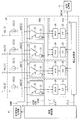
- FIG. 3 shows an example of a configuration of the reading unit 20.
- the reading unit 20 includes a plurality of constant current sources CS (constant current sources CS [0], CS [1], CS [2], CS [2], ...) And a plurality of AD conversion units ADC (AD conversion unit ADC). It has [0], ADC [1], ADC [2], ADC [3] ...) and a transfer scanning unit 29.
- a plurality of constant current sources CS are provided corresponding to a plurality of signal line VSLs.
- the 0th constant current source CS [0] is provided corresponding to the 0th signal line VSL [0]
- the 1st constant current source CS [1] is the 1st signal line.
- the second constant current source CS [2] is provided corresponding to the VSL [1]
- the second constant current source CS [2] is provided corresponding to the second signal line VSL [2]
- the third constant current source CS [3] is provided. It is provided corresponding to the third signal line VSL [3].
- One end of the constant current source CS is connected to the corresponding signal line VSL and the other end is grounded.
- Each of the plurality of constant current sources CS is configured to pass a predetermined current through the corresponding signal line VSL.
- a plurality of AD conversion units ADC are provided corresponding to a plurality of signal line VSLs.
- the 0th AD conversion unit ADC [0] is provided corresponding to the 0th signal line VSL [0]
- the 1st AD conversion unit ADC [1] is the 1st signal line.
- the second AD conversion unit ADC [2] is provided corresponding to the VSL [1]
- the second AD conversion unit ADC [2] is provided corresponding to the second signal line VSL [2]
- the third AD conversion unit ADC [3] is provided. It is provided corresponding to the third signal line VSL [2]. The same applies to the fourth and subsequent items.
- Each of the plurality of AD conversion units ADC is configured to convert the voltage of the signal SIG into a digital code CODE by performing AD conversion based on the signal SIG supplied from the pixel array 11.
- the AD conversion unit ADC has a comparison unit 21, a counter 24, and a latch 25.
- the comparison unit 21 is configured to generate a signal CMPO by performing a comparison operation based on the reference signal RAMP supplied from the reference signal generation unit 13 and the signal SIG supplied from the pixels P via the signal line VSL. To.
- the comparison unit 21 sets an operating point based on the control signals AZSW and AZN supplied from the image pickup control unit 15, and then performs a comparison operation.
- the comparison unit 21 has a power supply circuit 22 and a comparison circuit 23.
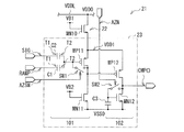
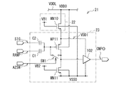
- FIG. 4A shows a configuration example of the comparison unit 21.
- the power supply voltage VDD0, the ground voltage VSS0, and the bias voltages VB1 and VB2 are supplied to the comparison unit 21.
- the power supply voltage VDD0 is supplied from the image pickup control unit 15 via the power supply line VDDL.
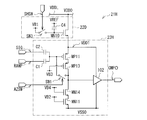
- the power supply circuit 22 of the comparison unit 21 has a transistor MN10.
- the comparison circuit 23 of the comparison unit 21 includes capacitive elements C1 and C2, transistors MP11, MN11, MP12 and MN12, switches SW1 and SW2, and capacitive elements C3.
- the transistors MP11 and MP12 are P-type MOS transistors, and the transistors MN10 to MN12 are N-type MOS transistors.
- the power supply voltage VDD0 is supplied to the back gates of the transistors MP11 and MP12
- the ground voltage VSS0 is supplied to the back gates of the transistors MN10 to MN12.
- a bias voltage VB1 is supplied to the gate of the transistor MN10, the drain is connected to the power supply line VDDL, and the source is connected to the sources of the transistors MP11 and MP12.
- the transistor MN10 operates as a so-called source follower to output the power supply voltage VDD1 from the source.
- Capacitive elements C1 and C2 have one end (terminal T1) and the other end (terminal T2).
- One end of the capacitive element C1 is connected to the reference signal generation unit 13, and the other end is connected to the other end of the capacitive element C2, the gate of the transistor MP11, and one end of the switch SW1.
- a reference signal RAMP generated by the reference signal generation unit 13 is supplied to one end of the capacitive element C1.
- One end of the capacitive element C2 is connected to the signal line VSL, and the other end is connected to the other end of the capacitive element C1, the gate of the transistor MP11, and one end of the switch SW1.
- the signal SIG generated by the pixel P is supplied to one end of the capacitive element C2.
- the gate of the transistor MP11 is connected to the other ends of the capacitive elements C1 and C2 and one end of the switch SW1, the drain is connected to the drain of the transistor MN11, the gate of the transistor MP12, and the other end of the switch SW1, and the sources are the transistors MN10 and MP12. Connected to the source of.
- the bias voltage VB2 is supplied to the gate of the transistor MN11, the drain is connected to the drain of the transistor MP11, the gate of the transistor MP12, and the other end of the switch SW1, and the ground voltage VSS0 is supplied to the source.
- the transistor MN11 is a load of the transistor MP11 and operates as a constant current source.
- the switch SW1 is configured to be turned on and off based on the control signal AZSW, one end is connected to the other end of the capacitive elements C1 and C2 and the gate of the transistor MP11, and the other end is the drain of the transistors MP11 and MN11 and the gate of the transistor MP12. Connected to.
- the transistors MP11, MN11, and switch SW1 form the first stage circuit 101 of the comparison circuit 23.
- the gate of the transistor MP12 is connected to the drain of the transistors MP11 and MN11 and the other end of the switch SW1, the drain is connected to the drain of the transistor MN12 and one end of the switch SW2, and the source is connected to the source of the transistors MN10 and MP11.
- the gate of the transistor MN12 is connected to one end of the capacitive element C3 and the other end of the switch SW2, the drain is connected to the drain of the transistor MP12 and one end of the switch SW2, and the ground voltage VSS0 is supplied to the source.
- the switch SW2 is configured to be turned on and off based on the control signal AZN, one end is connected to the drain of the transistors MP12 and MN12, and the other end is connected to the gate of the transistor MN12 and one end of the capacitive element C3.
- One end of the capacitive element C3 is connected to the gate of the transistor MN12 and the other end of the switch SW2, and the ground voltage VSS0 is supplied to the other end.
- the capacitance element C3 may be configured by using a MOS capacitor or the like, or may be configured by using, for example, the parasitic capacitance of the gate of the transistor MN12, the parasitic capacitance of the switch SW2, the parasitic capacitance of the wiring, or the like.
- the transistors MP12, MN12, the switch SW2, and the capacitive element C3 form a subsequent circuit 102 of the comparison circuit 23.
- the power supply circuit 22 generates the power supply voltage VDD1, and the comparison circuit 23 operates based on the power supply voltage VDD1 to perform the comparison operation based on the signal SIG and the reference signal RAMP. .. Specifically, the current generated by the transistor MN11 operating as a constant current source flows through the transistor MN10, and the transistor MN10 operates as a so-called source follower. As a result, the power supply circuit 22 generates the power supply voltage VDD1. In the comparison circuit 23, the operating point is set by turning on the switches SW1 and SW2, as will be described later.
- the comparison circuit 23 performs a comparison operation based on the reset voltage Vreset included in the reference signal RAMP and the signal SIG in the P-phase period TP, and is included in the reference signal RAMP and the signal SIG in the D-phase period TD.
- the comparison operation is performed based on the pixel voltage Vpix.
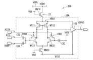
- the comparison unit 21 is configured as shown in FIG. 4A, but the present invention is not limited to this, and the comparison unit 21 may be configured as shown in FIG. 4B.
- the ground voltage VSS0 is supplied from the image pickup control unit 15 via the ground wire VSSL.
- the comparison unit 21A has a power supply circuit 22A and a comparison circuit 23A.
- the power supply circuit 22A has a transistor MP20.
- the comparison circuit 23A includes capacitive elements C11 and C12, transistors MN21, MP21, MN22 and MP22, switches SW11 and SW12, and capacitive elements C13.
- the transistors MP20 to MP22 are P-type MOS transistors, and the transistors MN21 and MN22 are N-type MOS transistors.
- a bias voltage VB1 is supplied to the gate of the transistor MP20, the drain is connected to the ground wire VSSL, and the source is connected to the sources of the transistors MN21 and MN22.
- the transistor MP20 outputs the ground voltage VSS1 from the source by operating as a so-called source follower.
- Capacitive elements C11 and C12 have one end and the other end.
- One end of the capacitive element C11 is connected to the reference signal generation unit 13, and the other end is connected to the other end of the capacitive element C12, the gate of the transistor MN21, and one end of the switch SW11.
- a reference signal RAMP generated by the reference signal generation unit 13 is supplied to one end of the capacitance element C11.
- One end of the capacitive element C12 is connected to the signal line VSL, and the other end is connected to the other end of the capacitive element C11, the gate of the transistor MN21, and one end of the switch SW11.
- the signal SIG generated by the pixel P is supplied to one end of the capacitive element C12.
- the gate of the transistor MN21 is connected to the other ends of the capacitive elements C11 and C12 and one end of the switch SW11, the drain is connected to the drain of the transistor MP21, the gate of the transistor MN22, and the other end of the switch SW11, and the sources are the transistors MP20 and MN22. Connected to the source of.
- the bias voltage VB2 is supplied to the gate of the transistor MP21, the drain is connected to the drain of the transistor MN21, the gate of the transistor MN22, and the other end of the switch SW11, and the power supply voltage VDD0 is supplied to the source.
- the transistor MP21 is a load of the transistor MN21 and operates as a constant current source.
- the switch SW11 is configured to be turned on and off based on the control signal AZSW, one end is connected to the other ends of the capacitive elements C11 and C12 and the gate of the transistor MN21, and the other end is the drain of the transistors MN21 and MP21 and the gate of the transistor MN22. Connected to.
- the transistors MN21, MP21, and switch SW11 form the first stage circuit 101 of the comparison circuit 23A.
- the gate of the transistor MN22 is connected to the drain of the transistors MN21 and MP21 and the other end of the switch SW11, the drain is connected to the drain of the transistor MP22 and one end of the switch SW12, and the source is connected to the source of the transistors MP20 and MN21.
- the gate of the transistor MP22 is connected to one end of the capacitive element C13 and the other end of the switch SW12, the drain is connected to the drain of the transistor MN22 and one end of the switch SW12, and the power supply voltage VDD0 is supplied to the source.
- the switch SW12 is configured to be turned on and off based on the control signal AZN, one end is connected to the drains of the transistors MN22 and MP22, and the other end is connected to the gate of the transistor MP22 and one end of the capacitive element C13.
- One end of the capacitive element C13 is connected to the gate of the transistor MP22 and the other end of the switch SW12, and the power supply voltage VDD0 is supplied to the other end.
- the transistors MN22, MP22, the switch SW12, and the capacitive element C13 form a subsequent circuit 102 of the comparison circuit 23A.
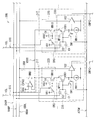
- FIG. 5 shows a connection example of the power line VDDL and the plurality of comparison units 21.
- the transistor MN11 of the comparison circuit 23 is shown using the symbol of the constant current source, and the subsequent circuit 102 (transistor MP12, MN12, switch SW2, and capacitance element C3) of the comparison circuit 23 is shown in the amplifier circuit. It is shown using a symbol.
- the imaging control unit 15 supplies the power supply voltage VDD0 to the plurality of comparison units 21 via the power supply line VDDL.
- the power supply circuit 22 (transistor MN10) generates a power supply voltage VDD1 based on the power supply voltage VDD0, and supplies the generated power supply voltage VDD1 to the comparison circuit 23.
- the comparison circuit 23 is adapted to generate a signal CMPO by performing a comparison operation based on the reference signal RAMP and the signal SIG.
- the counter 24 (FIG. 3) counts the pulse of the clock signal CLK supplied from the image pickup control unit 15 based on the signal CMPO supplied from the comparison unit 21 and the control signal CTL supplied from the image pickup control unit 15. It is configured to perform a counting operation.
- the latch 25 is configured to generate a digital code CODE based on the count value obtained by the counter 24 and hold the digital code CODE. Specifically, the latch 25 corresponds to the difference (CNTD-CNTP) between the count value CNTP obtained by the counter 24 in the P-phase period TP and the count value CNTD obtained by the counter 24 in the D-phase period TD. Generate a digital code CODE. Then, the latch 25 outputs this digital code CODE to the bus wiring BUS based on the control signal supplied from the transfer scanning unit 29.
- the transfer scanning unit 29 controls the latch 25s of the plurality of AD conversion units ADCs so as to sequentially output the digital code CODE to the bus wiring BUS based on the control signal CTL2 supplied from the image pickup control unit 15. It is composed of. Using this bus wiring BUS, the reading unit 20 sequentially transfers a plurality of digital code CODEs supplied from the plurality of AD conversion units ADC to the signal processing unit 14 as the image signal DATA0.
- the signal processing unit 14 (FIG. 1) generates an image signal DATA by performing predetermined signal processing on the image signal DATA0 based on an instruction from the imaging control unit 15, and outputs the image signal DATA. It is configured as follows.
- the image pickup control unit 15 controls the operation of the image pickup device 1 by supplying control signals to the drive unit 12, the reference signal generation unit 13, the reading unit 20, and the signal processing unit 14 and controlling the operation of these circuits. It is configured to do. Specifically, the image pickup control unit 15 supplies a control signal to the drive unit 12, so that the drive unit 12 sequentially drives a plurality of pixels P in the pixel array 11 in units of pixel lines L. Control. Further, the imaging control unit 15 controls the reference signal generation unit 13 to generate the reference signal RAMP by supplying the control signal to the reference signal generation unit 13.
- the imaging control unit 15 supplies the power supply voltage VDD0 and the bias voltages VB1 and VB2 to the reading unit 20, and also supplies the control signals AZSW, AZN, CTL, CTL2 and the clock signal CLK to the reading unit. 20 is controlled to generate the image signal DATA0 by performing AD conversion based on the signal SIG. Further, the imaging control unit 15 controls the operation of the signal processing unit 14 by supplying a control signal to the signal processing unit 14.
- each block shown in FIG. 1 may be formed on, for example, one semiconductor substrate or a plurality of semiconductor substrates.
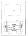
- FIG. 6 shows a mounting example of the image pickup apparatus 1 when formed on one semiconductor substrate 200.
- a pixel array 11 is arranged on the semiconductor substrate 200, and a drive unit 12 is arranged on the left side of the pixel array 11.
- a reading unit 20 is arranged below the pixel array 11.
- a constant current source unit 201 including a plurality of constant current sources CS
- a comparison circuit unit 202 including a plurality of comparison units 21, a counter unit 203 including a plurality of counters 24, and a plurality of latches 25 are used.
- the latch portion 204 including the latch portion 204 and the transfer scanning portion 29 are arranged in this order.
- a reference signal generation unit 13 and an imaging control unit 15 are arranged on the left side of the reading unit 20.
- a signal processing unit 14 is arranged to the right of the pixel array 11 and the reading unit 20.
- FIG. 7 shows a mounting example of the image pickup apparatus 1 when formed on two semiconductor substrates 211 and 212.
- the pixel array 11 is arranged on the semiconductor substrate 211, and the reading unit 20, the driving unit 12, the reference signal generation unit 13, the signal processing unit 14, and the imaging control unit 15 are arranged on the semiconductor substrate 212.
- the semiconductor substrates 211 and 212 are superposed on each other.
- a plurality of signal line VSLs arranged on the semiconductor substrate 211 are electrically connected to the reading unit 20 arranged on the semiconductor substrate 212 via, for example, a TSV (Through Silicon Via), and the semiconductor substrate 211 is formed.
- TSV Thinough Silicon Via
- a plurality of control lines TGL, RSTL, and SELL arranged in the above are electrically connected to a drive unit 12 arranged on the semiconductor substrate 212 via, for example, a TSV.
- a reading unit 20 is arranged on the semiconductor substrate 212, a driving unit 12, a reference signal generation unit 13, and an imaging control unit 15 are arranged on the left side of the reading unit 20, and a signal processing unit is arranged on the right side of the reading unit 20. 14 is arranged.
- a constant current source unit 201 including a plurality of constant current sources CS, a comparison circuit unit 202 including a plurality of comparison units 21, a counter unit 203 including a plurality of counters 24, and a plurality of latches 25 are used.
- the latch portion 204 including the latch portion 204 and the transfer scanning portion 29 are arranged in this order.
- the semiconductor manufacturing process specialized in the formation of pixels is used by mainly arranging the pixel array 11 on the semiconductor substrate 211.
- the semiconductor substrate 211 can be manufactured. That is, since the semiconductor substrate 211 has no circuit other than the pixel array 11, for example, even if a special manufacturing process is used to form the pixels, the manufacturing process affects the circuits other than the pixel array 11. None.
- the semiconductor manufacturing process specialized in the formation of pixels can be used in the image pickup device 1, the image pickup characteristics in the image pickup device 1 can be improved.
- the pixel P corresponds to a specific example of the "first pixel” in the present disclosure.
- the comparison unit 21 corresponds to a specific example of the “first comparison unit” in the present disclosure.
- the power supply circuit 22 corresponds to a specific example of the “first power supply circuit” in the present disclosure.
- the comparison circuit 23 corresponds to a specific example of the “first comparison circuit” in the present disclosure.
- the transistor MN10 corresponds to a specific example of the "first power supply transistor” in the present disclosure.
- the capacitive element C1 corresponds to a specific example of the "first capacitive element” in the present disclosure.
- the capacitive element C2 corresponds to a specific example of the "second capacitive element” in the present disclosure.
- the transistor MP11 corresponds to a specific example of the "first transistor” in the present disclosure.
- the switch SW1 corresponds to a specific example of the "first switch” in the present disclosure.
- the transistor MN11 corresponds to a specific example of the "first current source” in the present disclosure.
- the transistor MP12 corresponds to a specific example of the "second transistor” in the present disclosure.
- the transistor MN12 corresponds to a specific example of the "third transistor” in the present disclosure.
- the switch SW2 corresponds to a specific example of the "second switch” in the present disclosure.
- the drive unit 12 sequentially drives a plurality of pixels P in the pixel array 11 in pixel line L units based on an instruction from the image pickup control unit 15.
- the pixel P outputs the reset voltage Vreset as a signal SIG
- the D-phase period TD outputs the pixel voltage Vpix corresponding to the received light amount as a signal SIG.
- the reference signal generation unit 13 generates the reference signal RAMP based on the instruction from the image pickup control unit 15.
- the reading unit 20 generates the image signal DATA0 by performing AD conversion based on the signal SIG supplied from the pixel array 11 via the signal line VSL based on the instruction from the imaging control unit 15.
- the signal processing unit 14 generates the image signal DATA by performing predetermined signal processing on the image signal DATA0 based on the instruction from the image pickup control unit 15.
- the image pickup control unit 15 controls the operation of the image pickup device 1 by supplying control signals to the drive unit 12, the reference signal generation unit 13, the reading unit 20, and the signal processing unit 14 and controlling the operation of these circuits.
- the plurality of pixels P accumulate electric charges according to the amount of light received, and output the pixel voltage Vpix according to the amount of light received as a signal SIG. Then, the reading unit 20 performs AD conversion based on this signal SIG. This operation will be described in detail below.
- FIG. 8 shows an example of an operation of scanning a plurality of pixels P in the pixel array 11.
- the image pickup apparatus 1 performs the exposure start drive D1 in order from the top in the vertical direction with respect to the pixel array 11 during the period from timing t0 to t1.
- the drive unit 12 sequentially selects the pixel line L by generating, for example, the control signals STG and SRST, and sequentially turns on the transistors TG and RST in the pixel P for a predetermined length of time. To do.
- the voltage of the floating diffusion FD and the voltage of the cathode of the photodiode PD are set to the power supply voltage VDD.
- the photodiode PD begins to accumulate electric charges according to the amount of light received. In this way, the exposure period T starts sequentially in the plurality of pixels P.
- the image pickup device 1 performs read drive D2 in order from the top in the vertical direction with respect to the pixel array 11 during the period from timing t2 to t3. Specifically, the drive unit 12 sequentially selects the pixel line L by generating control signals STG and SRST, as will be described later. As a result, the pixel P outputs the reset voltage Vreset as a signal SIG in the P-phase period TP, and outputs the pixel voltage Vpix as a signal SIG in the D-phase period TD.
- the reading unit 20 generates a digital code CODE by performing AD conversion based on this signal SIG.
- the image pickup apparatus 1 repeats such an exposure start drive D1 and a read drive D2. As a result, the image pickup device 1 can obtain a series of captured images.
- the read drive D2 will be described in detail.
- the operation of the pixel P1 and the AD conversion unit ADC (AD conversion unit ADC1) connected to the pixel P1 and the pixel P1 will be described in detail, focusing on a certain pixel P (pixel P1) among the plurality of pixels P.
- FIG. 9 shows an operation example of the read drive D2 in the pixel P1 of interest
- (A) shows the waveform of the control signal SSEL
- (B) shows the waveform of the control signal SRST
- (C) shows the waveform of the control signal SRST.
- the waveform of the control signal STG is shown
- (D) shows the waveform of the signal SIG
- (E) shows the waveform of the control signal AZSW
- (F) shows the waveform of the reference signal RAMP
- G) shows the AD conversion unit.
- the waveform of the gate voltage Vg of the transistor MP11 in the comparison unit 21 of the ADC1 is shown
- (H) shows the waveform of the signal CMPO in the AD conversion unit ADC1.
- the waveform of the control signal AZN is the same as the waveform of the control signal AZSW.
- the pixel P1 performs a reset operation to output a reset voltage Vreset, and the AD conversion unit ADC1 performs AD conversion based on the reset voltage Vreset in the P phase period TP. I do. Then, after that, the pixel P1 performs a charge transfer operation to output the pixel voltage Vpix, and the AD conversion unit ADC1 performs AD conversion based on the pixel voltage Vpix in the D phase period TD. This operation will be described in detail below.
- the drive unit 12 changes the voltage of the control signal SSEL from a low level to a high level (FIG. 9A).
- the transistor SEL is turned on, and the pixel P1 is electrically connected to the signal line VSL.
- the drive unit 12 changes the voltage of the control signal SRST from a low level to a high level (FIG. 9B).
- the transistor RST is turned on, and the voltage of the floating diffusion FD is set to the power supply voltage VDD (reset operation).
- the pixel P1 outputs a voltage (reset voltage Vreset) corresponding to the voltage of the floating diffusion FD at this time. In this way, the voltage of the signal SIG becomes the reset voltage Vreset (FIG. 9 (D)).
- the reference signal generation unit 13 sets the reference signal RAMP to the voltage V1 (FIG. 9 (F)). Further, at this timing t11, the imaging control unit 15 changes the voltages of the control signals AZSW and AZN from a low level to a high level (FIG. 9 (E)). As a result, in the comparison unit 21 of the AD conversion unit ADC1, both the switches SW1 and SW2 are turned on. When the switch SW1 is turned on, the gate voltage Vg of the transistor MP11 becomes the same voltage (voltage V2) as the drain voltage of the transistor MP11 (FIG. 9 (G)), and the voltages of the capacitive elements C1 and C2 are set. To.
- the comparison unit 21 performs the operating point setting operation.
- the drive unit 12 changes the voltage of the control signal SRST from a high level to a low level (FIG. 9B). As a result, in the pixel P1, the transistor RST is turned off.
- the imaging control unit 15 changes the voltages of the control signals AZSW and AZN from a high level to a low level (FIG. 9 (E)).
- the comparison unit 21 of the AD conversion unit ADC1 both the switches SW1 and SW2 are turned off, and the operating point setting operation is completed.
- the comparison unit 21 operates so as to compare the gate voltage Vg and the voltage V2.
- the reference signal generation unit 13 reduces the voltage of the reference signal RAMP from the voltage V1 to the voltage V4 (FIG. 9 (F)).
- the comparison unit 21 of the AD conversion unit ADC1 the gate voltage Vg of the transistor MP11 becomes lower than the voltage V2 (FIG. 9 (G)), so that the voltage of the signal CMPO decreases (FIG. 9 (H)).
- the comparison unit 21 compares the gate voltage Vg with the voltage V2, and since the gate voltage Vg is lower than this voltage V2, the voltage of the signal CMPO is set to a low level.
- the AD conversion unit ADC1 performs AD conversion based on the reset voltage Vreset. Specifically, first, at the timing t15, the reference signal generation unit 13 starts increasing the voltage of the reference signal RAMP from the voltage V4 by a predetermined degree of change (FIG. 9F). In response to this, in the comparison unit 21 of the AD conversion unit ADC1, the gate voltage Vg of the transistor MP11 begins to increase (FIG. 9 (G)). Further, at this timing t15, the imaging control unit 15 starts generating the clock signal CLK. The counter 24 of the AD conversion unit ADC1 counts the pulse of the clock signal CLK by performing a counting operation.
- the comparison unit 21 of the AD conversion unit ADC1 changes the voltage of the signal CMPO from a low level to a high level (FIG. 9 (H)). That is, the comparison unit 21 compares the gate voltage Vg and the voltage V2, and since the gate voltage Vg exceeds this voltage V2, the voltage of the signal CMPO is changed from a low level to a high level.
- the counter 24 of the AD conversion unit ADC1 stops the counting operation based on the transition of the signal CMPO. At this time, the count value of the counter 24 is CNTP.
- the latch 25 of the AD conversion unit ADC1 latches this count value CNTP as a count value in the P phase period TP. Then, the counter 24 is reset.
- the reference signal generation unit 13 sets the voltage of the reference signal RAMP to the voltage V1 with the end of the P-phase period TP. Further, the imaging control unit 15 stops the generation of the clock signal CLK at this timing t17.
- the drive unit 12 changes the voltage of the control signal STG from a low level to a high level (FIG. 9 (C)).
- the transistor TG is turned on, and the charge generated by the photodiode PD is transferred to the floating diffusion FD (charge transfer operation).
- the pixel P1 outputs a voltage (pixel voltage Vpix) corresponding to the voltage of the floating diffusion FD at this time.
- the voltage of the signal SIG becomes the pixel voltage Vpix (FIG. 9 (D)).
- FIG. 9 shows an example of two pixel voltages Vpix (pixel voltages Vpix1 and Vpix2) that are different from each other.
- the gate voltage Vg of the transistor MP11 decreases in the comparison unit 21 of the AD conversion unit ADC1 (FIG. 9 (G)).
- the gate voltage Vg changes by a voltage corresponding to the pixel voltage Vpix.
- the voltage of the signal CMPO decreases (FIG. 9 (H)). That is, the comparison unit 21 compares the gate voltage Vg and the voltage V2, and since the gate voltage Vg is lower than this voltage V2, the voltage of the signal CMPO is set to a low level.
- the drive unit 12 changes the voltage of the control signal STG from a high level to a low level (FIG. 9 (C)). As a result, the transistor TG is turned off in the pixel P1.
- the reference signal generation unit 13 reduces the voltage of the reference signal RAMP from the voltage V1 to the voltage V4 (FIG. 9 (F)).
- the gate voltage Vg of the transistor MP11 decreases (FIG. 9 (G)).
- the AD conversion unit ADC1 performs AD conversion based on the pixel voltage Vpix. Specifically, first, at the timing t20, the reference signal generation unit 13 starts to increase the voltage of the reference signal RAMP from the voltage V4 by a predetermined degree of change (FIG. 9F). In response to this, in the comparison unit 21 of the AD conversion unit ADC1, the gate voltage Vg of the transistor MP11 begins to increase (FIG. 9 (G)). Further, at this timing t20, the imaging control unit 15 starts generating the clock signal CLK. The counter 24 of the AD conversion unit ADC1 counts the pulse of the clock signal CLK by performing a counting operation.
- the comparison unit 21 of the AD conversion unit ADC1 changes the voltage of the signal CMPO from a low level to a high level (FIG. 9 (H)). That is, the comparison unit 21 compares the gate voltage Vg and the voltage V2, and since the gate voltage Vg exceeds the voltage V2, the voltage of the signal CMPO is changed from a low level to a high level.
- the comparison unit 21 of the AD conversion unit ADC1 changes the voltage of the signal CMPO from a low level to a high level (FIG. 9 (H)).
- the counter 24 of the AD conversion unit ADC1 stops the counting operation based on the transition of this signal CMPO. At this time, the count value of the counter 24 is CNT.
- the latch 25 of the AD conversion unit ADC1 latches this count value CNT as a count value in the D phase period TD. Then, the counter 24 is reset.
- the reference signal generation unit 13 sets the voltage of the reference signal RAMP to the voltage V1 with the end of the D-phase period TD (FIG. 9 (F)). Further, the imaging control unit 15 stops the generation of the clock signal CLK at this timing t23. Then, the drive unit 12 changes the voltage of the control signal SSEL from a high level to a low level at this timing t23 (FIG. 9A). As a result, in the pixel P1, the transistor SEL is turned off, and the pixel P1 is electrically disconnected from the signal line VSL.
- the latch 25 of the AD conversion unit ADC1 determines the difference (CNTD-CNTP) between the count value CNTP obtained by the counter 24 in the P-phase period TP and the count value CNTD obtained by the counter 24 in the D-phase period TD. Generate the corresponding digital code CODE.
- the image pickup apparatus 1 acquires the count value CNTP by performing the counting operation based on the reset voltage Vreset in the P-phase period TP, and counts by performing the counting operation based on the pixel voltage Vpix in the D-phase period TD. Changed to get the value CNT. Then, in the image pickup apparatus 1, the digital code CODE corresponding to the difference between the count values CNTP and CNTD (CNTD-CNTP) is generated. Since the image pickup apparatus 1 performs such correlation double sampling, the noise component included in the pixel voltage Vpix can be removed, and as a result, the image quality of the captured image can be improved.
- each of the plurality of comparison units 21 has a power supply circuit 22.
- interference between a plurality of AD conversion units ADC can be suppressed. That is, for example, when the power supply circuit 22 is not provided in each of the plurality of comparison units 21, noise is generated in the power supply voltage VDD0 due to the transient current when the comparison unit 21 transitions the signal CMPO in a certain AD conversion unit ADC. May occur. In this case, this noise may affect the operation of other AD conversion units via the power supply line VDDL.
- the power supply circuit 22 is provided in each of the plurality of comparison units 21, noise of the power supply voltage VDD0 generated by the transient current when the comparison unit 21 transitions the signal CMPO in a certain AD conversion unit ADC.
- the possibility of streaking in the captured image can be reduced.
- the image quality of the captured image can be improved in the image pickup device 1.
- each of the plurality of comparison units has a power supply circuit, the image quality of the captured image can be improved.
- the comparison circuit 23 of the comparison unit 21 shown in FIG. 4A is provided with four transistors MP11, MN11, MP12, and MN12, but the present invention is not limited to this.
- the transistor MN13 may be further provided as in the comparison circuit 23B of the comparison unit 21B shown in FIG. 10A.
- This transistor MN13 is an N-type MOS transistor, a signal CMPO is supplied to the gate, the drain is connected to the source of the transistors MN10, MP11, MP12, and the source is the drain of the transistors MP11, MN11, the gate of the transistor MP12. It is connected to the other end of the switch SW1.
- the transistor MN13 corresponds to a specific example of the "fourth transistor” in the present disclosure.
- the transistor MN13 controls the drain voltage of the transistor MN11 operating as a constant current source so as not to become too low based on the voltage of the signal CMPO. Thereby, for example, the constant current property of the transistor MN11 can be maintained, and the interference between the plurality of AD conversion units ADC can be suppressed.
- the present modification is applied to the comparison unit 21 (FIG. 4A), but for example, the present modification may be applied to the comparison unit 21A (FIG. 4B).
- the transistor MP23 may be provided as in the comparison circuit 23C of the comparison unit 21C shown in FIG. 10B.
- This transistor MP23 is a P-type MOS transistor, and a signal CMPO is supplied to the gate, the drain is connected to the source of the transistors MP20, MN21, and MN22, and the source is the drain of the transistors MN21 and MP21 and the gate of the transistor MN22. It is connected to the other end of the switch SW11.
- the transistor MP23 is controlled based on the voltage of the signal CMPO so that the drain voltage of the transistor MP21 operating as a constant current source does not become too high. Thereby, for example, the constant current property of the transistor MP21 can be maintained, and the interference between the plurality of AD conversion units ADC can be suppressed.
- the bias voltage VB1 is always supplied to the gate of the transistor MN10, but the present invention is not limited to this. Instead of this, for example, a sample hold circuit may be provided to supply the bias voltage VB1 to the gate of the transistor MN10 only for a predetermined period. An example in which this modification is applied to the comparison unit 21B shown in FIG. 10A will be described in detail below.
- FIG. 11A shows a configuration example of the comparison unit 21D according to this modification.
- the comparison unit 21D has a power supply circuit 22D and a comparison circuit 23B.
- the power supply circuit 22D has a capacitance element C4 and a switch SW3. One end of the capacitive element C4 is connected to the gate of the transistor MN10 and one end of the switch SW3, and a DC voltage VREF is supplied to the other end. This voltage VREF is generated by the imaging control unit 15.
- the capacitance element C4 may be configured by using a MOS capacitor or the like, or may be configured by using, for example, the parasitic capacitance of the gate of the transistor MN10, the parasitic capacitance of the switch SW3, the parasitic capacitance of the wiring, or the like.
- the switch SW3 is configured to be turned on and off based on the control signal SHSW, one end is connected to the gate of the transistor MN10 and one end of the capacitive element C4, and the bias voltage VB1 is supplied to the other end.
- the control signal SHSW is generated by the imaging control unit 15.
- the capacitive element C4 and the switch SW3 form a sample hold circuit.
- the capacitive element C4 corresponds to a specific example of the "fourth capacitive element” in the present disclosure.
- the switch SW3 corresponds to a specific example of the "fourth switch” in the present disclosure.
- the switch SW3 is turned on during the period when the switches SW1 and SW2 are turned on, and is turned off during the period when the switches SW1 and SW2 are turned off. Specifically, in the read drive D2 shown in FIG. 9, the switch SW3 is turned on during the period from timing t11 to t13. As a result, the gate voltage of the transistor MN10 is set to the bias voltage VB1. Then, the switch SW3 is turned off during the period from timing t13 to t23. As a result, the gate voltage of the transistor MN10 is maintained at this bias voltage VB1. In the comparison unit 21D, the switch SW3 is turned off during the P-phase period TP and the D-phase period TD.
- FIG. 11B shows a configuration example of the comparison unit 21E when the present modification is applied to the comparison unit 21C (FIG. 10B).
- the comparison unit 21E has a power supply circuit 22E and a comparison circuit 23C.
- the power supply circuit 22E has a capacitance element C14 and a switch SW13. One end of the capacitive element C14 is connected to the gate of the transistor MP20 and one end of the switch SW13, and the voltage VREF is supplied to the other end.
- the switch SW13 is configured to be turned on and off based on the control signal SHSW, one end is connected to the gate of the transistor MP20 and one end of the capacitive element C14, and the bias voltage VB1 is supplied to the other end.
- the comparison unit 21E can suppress the interference between the plurality of AD conversion units ADC as in the comparison unit 21D.
- the bias voltage VB2 is always supplied to the gate of the transistor MN11 operating as a current source, but the present invention is limited to this. is not.
- a sample hold circuit may be provided to supply the bias voltage VB2 to the gate of the transistor MN11 only for a predetermined period.
- FIG. 12A shows a configuration example of the comparison unit 21F according to this modification.
- the comparison unit 21F has a power supply circuit 22D and a comparison circuit 23F.
- the comparison circuit 23F has a capacitance element C5 and a switch SW4. One end of the capacitive element C5 is connected to the gate of the transistor MN11 and one end of the switch SW4, and a DC voltage VREF is supplied to the other end. This voltage VREF is generated by the imaging control unit 15.
- the capacitance element C5 may be configured by using a MOS capacitor or the like, or may be configured by using, for example, the parasitic capacitance of the gate of the transistor MN11, the parasitic capacitance of the switch SW4, the parasitic capacitance of the wiring, or the like.
- the switch SW4 is configured to be turned on and off based on the control signal SHSW2, one end is connected to the gate of the transistor MN11 and one end of the capacitive element C5, and the bias voltage VB2 is supplied to the other end.
- the control signal SHSW2 is generated by the image pickup control unit 15.
- the capacitive element C5 and the switch SW4 form a sample hold circuit.
- the switch SW4 corresponds to a specific example of the "sixth switch" in the present disclosure.
- the switch SW4 is turned on during the period when the switches SW1 and SW2 are turned on, and is turned off during the period when the switches SW1 and SW2 are turned off. Specifically, in the read drive D2 shown in FIG. 9, the switch SW4 is turned on during the period from timing t11 to t13. As a result, the gate voltage of the transistor MN11 is set to the bias voltage VB2. Then, the switch SW4 is turned off during the period from timing t13 to t23. As a result, the gate voltage of the transistor MN11 is maintained at this bias voltage VB2. In the comparison unit 21F, the switch SW4 is turned off during the P-phase period TP and the D-phase period TD.
- FIG. 12B shows a configuration example of the comparison unit 21G when the present modification is applied to the comparison unit 21E (FIG. 11B).
- the comparison unit 21G has a power supply circuit 22E and a comparison circuit 23G.
- the comparison circuit 23G has a capacitance element C15 and a switch SW14. One end of the capacitive element C15 is connected to the gate of the transistor MP21 and one end of the switch SW14, and the voltage VREF is supplied to the other end.
- the switch SW14 is configured to be turned on and off based on the control signal SHSW2, one end is connected to the gate of the transistor MP21 and one end of the capacitive element C15, and the bias voltage VB2 is supplied to the other end.
- the comparison unit 21G can suppress interference between the plurality of AD conversion units ADCs, as in the comparison unit 21F.
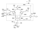
- the first stage circuit 101 of the comparison circuit 23 is configured by using the two transistors MP11 and MN11, but the present invention is not limited to this. Instead of this, for example, as in the comparison unit 21H shown in FIG. 13, the first stage circuit 101 may be configured by using more transistors.
- the first stage circuit 101 of the comparison unit 21H has transistors MN11, MP11, MP13, and MN14.
- the transistor MP13 is a P-type MOS transistor, a bias voltage VB3 is supplied to the gate, the drain is connected to the drain of the transistor MN14, the input terminal of the subsequent circuit 102, and the other end of the switch SW1, and the source is the transistor MP11. Connected to the drain of.
- the bias voltage VB3 is generated by the image pickup control unit 15.
- the transistor MP11 is source-grounded, and the transistor MP13 is gate-grounded. As a result, the transistor MP11 and the transistor MP13 form a cascode circuit.
- the transistor MN14 is an N-type MOS transistor, a bias voltage VB4 is supplied to the gate, the drain is connected to the drain of the transistor MP13, the input terminal of the subsequent circuit 102, and the other end of the switch SW1, and the source is the transistor MN11. Connected to the drain of.
- the bias voltage VB4 is generated by the image pickup control unit 15.
- the transistors MN11 and MN14 form a cascode circuit.
- the small signal gain can be increased, so that a more stable comparison operation can be realized. Further, by providing the transistors MP13 and MN14, kickback noise from the subsequent circuit 102 can be reduced.
- the transistor MN10 operates as a source follower in the power supply circuit 22, but the present invention is not limited to this. Instead of this, for example, a plurality of transistors may be provided so that the plurality of transistors operate as a multi-stage source follower. The present modification will be described in detail below with some examples.
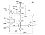
- FIG. 14 shows a configuration example of the comparison unit 21J according to this modification.
- the comparison unit 21J has a power supply circuit 22J and a comparison circuit 23.
- the power supply circuit 22J includes transistors MN10 and MN15, a capacitance element C6, and a switch SW5.
- a bias voltage VB1 is supplied to the gate of the transistor MN10, the drain is connected to the power supply line VDDL, and the source is connected to the drain of the transistor MN15.
- the transistor MN15 is an N-type MOS transistor, the gate is connected to one end of the capacitive element C6 and one end of the switch SW5, the drain is connected to the source of the transistor MN10, and the source is the source of the transistor MP11 and the power supply of the subsequent circuit 102. Connected to the terminal.
- One end of the capacitive element C6 is connected to the gate of the transistor MN15 and one end of the switch SW5, and a DC voltage VREF is supplied to the other end.
- the voltage VREF is generated by the imaging control unit 15.
- the switch SW5 is configured to be turned on and off based on the control signal SHSW, one end is connected to the gate of the transistor MN15 and one end of the capacitive element C6, and the bias voltage VB5 is supplied to the other end.
- the control signal SHSW and the bias voltage VB5 are generated by the image pickup control unit 15.
- the capacitive element C6 and the switch SW5 form a sample hold circuit.
- the switch SW5 is turned on during the period when the switch SW1 is turned on, and is turned off during the period when the switch SW1 is turned off.
- the transistor MN15 corresponds to a specific example of the "second power supply transistor" in the present disclosure.
- the switch SW5 corresponds to a specific example of the "fifth switch” in the present disclosure.
- the comparison unit 21J the current generated by the transistor MN11 operating as a constant current source flows through the transistors MN10 and MN15, and the transistors MN10 and MN15 operate as a two-stage source follower.
- the power supply circuit 22J generates the power supply voltage VDD1.
- the comparison unit 21J is provided with a two-stage source follower, noise of the power supply voltage VDD0 generated by the transient current when the comparison unit 21J transitions the signal CMPO in a certain AD conversion unit ADC.
- FIG. 15 shows a configuration example of another comparison unit 21K according to this modification.
- the comparison unit 21K has a power supply circuit 22K and a comparison circuit 23.
- the power supply circuit 22K includes transistors MN10 and MN15, an operational amplifier OPA, a capacitance element C6, and a switch SW5.
- the gate of the transistor MN10 is connected to the output terminal of the operational amplifier OPA, the drain is connected to the power supply line VDDL, and the source is connected to the drain of the transistor MN15 and the inverting input terminal of the operational amplifier OPA.
- a bias voltage VB1 is supplied to the non-inverting input terminal of the operational amplifier OPA, the inverting input terminal is connected to the source of the transistor MN10 and the drain of the transistor MN15, and the output terminal is connected to the gate of the transistor MN10.
- the gate of the transistor MN15 is connected to one end of the capacitive element C6 and one end of the switch SW5, the drain is connected to the source of the transistor MN10 and the inverting input terminal of the operational amplifier OPA, and the source is the source of the transistor MP11 and the power supply terminal of the subsequent circuit 102. Connected to. One end of the capacitive element C6 is connected to the gate of the transistor MN15 and one end of the switch SW5, and a DC voltage VREF is supplied to the other end. The voltage VREF is generated by the imaging control unit 15.
- the switch SW5 is configured to be turned on and off based on the control signal SHSW, one end is connected to the gate of the transistor MN15 and one end of the capacitive element C6, and the bias voltage VB5 is supplied to the other end.
- the control signal SHSW and the bias voltage VB5 are generated by the image pickup control unit 15.
- the capacitive element C6 and the switch SW5 form a sample hold circuit.
- the switch SW5 is turned on during the period when the switch SW1 is turned on, and is turned off during the period when the switch SW1 is turned off.
- the comparison unit 21K a negative feedback operation is performed so that the source voltage of the transistor MN10 becomes equal to the bias voltage VB1. Then, the current generated by the transistor MN11 operating as a constant current source flows through the transistors MN10 and MN15, and the transistors MN10 and MN15 operate as a two-stage source follower. Then, the power supply circuit 22K generates the power supply voltage VDD1. As a result, the comparison unit 21K can suppress interference between the plurality of AD conversion units ADCs, as in the comparison unit 21J.
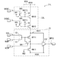
- FIG. 16 shows a configuration example of another comparison unit 21L according to this modification.
- the comparison unit 21L has a power supply circuit 22L and a comparison circuit 23.
- the power supply circuit 22L includes transistors MN10 and MN15, capacitive elements C4 and C6, and switches SW3 and SW5.
- the gate of the transistor MN10 is connected to one end of the capacitive element C4 and one end of the switch SW3, the drain is connected to the power supply line VDDL, and the source is connected to the drain of the transistor MN15.
- One end of the capacitive element C4 is connected to the gate of the transistor MN10 and one end of the switch SW3, and a DC voltage VREF1 is supplied to the other end.
- the voltage VREF1 is generated by the image pickup control unit 15.
- the switch SW3 is configured to be turned on and off based on the control signal SHSW1, one end is connected to the gate of the transistor MN10 and one end of the capacitive element C4, and the bias voltage VB1 is supplied to the other end.
- the control signal SHSW1 and the bias voltage VB1 are generated by the image pickup control unit 15.
- the switch SW3 is turned on during the period when the switch SW1 is turned on, and is turned off during the period when the switch SW1 is turned off.
- the gate of the transistor MN15 is connected to one end of the capacitive element C6 and one end of the switch SW5, the drain is connected to the source of the transistor MN10, and the source is connected to the source of the transistor MP11 and the power supply terminal of the subsequent circuit 102.
- One end of the capacitive element C6 is connected to the gate of the transistor MN15 and one end of the switch SW5, and the DC voltage VREF2 is supplied to the other end.
- the voltage VREF2 is generated by the image pickup control unit 15.
- the switch SW5 is configured to be turned on and off based on the control signal SHSW2, one end is connected to the gate of the transistor MN15 and one end of the capacitive element C6, and the bias voltage VB5 is supplied to the other end.
- the control signal SHSW2 and the bias voltage VB5 are generated by the image pickup control unit 15.
- the switch SW5 is turned on during the period when the switch SW1 is turned on, and is turned off during the period when the switch SW1 is turned off.
- the comparison unit 21L the current generated by the transistor MN11 operating as a constant current source flows through the transistors MN10 and MN15, and the transistors MN10 and MN15 operate as a two-stage source follower. Then, the power supply circuit 22L generates the power supply voltage VDD1. As a result, the comparison unit 21L can suppress interference between the plurality of AD conversion units ADCs, as in the comparison unit 21J.
- FIG. 18 shows a configuration example of the comparison unit 21M according to this modification.
- the comparison unit 21M has a power supply circuit 22M.
- the back gate of the transistor MN10 is connected to the source of the transistor MN10.
- the transistor MN10 is formed in, for example, a P-well that is electrically insulated from the P-type semiconductor substrate by a deep N-well.
- the gate-source voltage Vgs of the transistor MN10 can be reduced, so that, for example, the power supply voltage VDD0 can be made lower, and power consumption can be reduced.
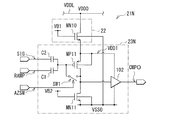
- FIG. 19 shows a configuration example of another comparison unit 21N according to this modification.
- the comparison unit 21N has a comparison circuit 23N.
- the back gate of the transistor MP11 is connected to the source of the transistor MP11.
- the absolute value of the gate-source voltage Vgs of the transistor MP11 can be reduced, so that, for example, the power supply voltage VDD0 can be made lower and the power consumption can be reduced.
- This comparison unit 21N is effective when a manufacturing process in which a deep N well cannot be formed is used.
- FIG. 20 shows a configuration example of another comparison unit 21P according to this modification.
- the comparison unit 21P has a power supply circuit 22M and a comparison circuit 23N. That is, the back gate of the transistor MN10 is connected to the source of the transistor MN10, and the back gate of the transistor MP11 is connected to the source of the transistor MP11.
- the absolute value of the gate-source voltage Vgs of the transistors MN10 and MP11 can be reduced together, so that, for example, the power supply voltage VDD0 can be made lower and the power consumption can be reduced.
- the comparison unit 21P since both back gates of the transistors MP11 and MN10 are connected to the sources of these transistors, these back gates are individually driven with the AD conversion unit ADC as a unit. Therefore, it is possible to suppress interference between a plurality of AD conversion units ADC.
- FIG. 21 shows a configuration example of the reading unit 20Q in the imaging device 1Q according to this modification.
- the reading unit 20Q has a plurality of comparison units 21Q and a voltage generating unit 16Q.
- Each of the plurality of comparison units 21Q has a power supply circuit 22Q.
- the back gates of the transistors MN10 of the plurality of power supply circuits 22Q are connected to each other.
- a DC voltage VDC is supplied to the back gates of these transistors MN10.
- These plurality of transistors MN10 are formed in one P-well.
- the voltage generation unit 16Q is configured to generate a voltage VDC.
- the voltage VDC is set to a voltage such that the PN junction composed of the source and P well of the transistor MN10 is reverse biased.
- the voltage VDC is supplied to the back gates of the plurality of transistors MN10.
- the absolute value of the gate-source voltage Vgs of the transistor MN10 can be reduced, so that, for example, the power supply voltage VDD0 can be made lower and the power consumption can be reduced. Can be done.
- the image pickup apparatus 1Q since a plurality of transistors MN10 are provided in one P well, for example, the area of the well contact can be reduced as compared with the case where a plurality of transistors MN10 are provided in each of the plurality of P wells. Therefore, the layout area can be reduced.
- the output terminal of the power supply circuit 22 is connected to the comparison circuit 23 in each comparison unit 21 of the plurality of AD conversion units ADC, but the present invention is not limited to this. Instead of this, for example, the output terminals of the power supply circuits 22 of the two or more AD conversion unit ADCs may be connected to each other, and these output terminals may be connected to the comparison circuit 23 of the two or more AD conversion unit ADCs. ..
- the present modification will be described in detail below.
- the reading unit 20R has a plurality of AD conversion units ADC.
- the output terminals of the power supply circuit 22 in the two AD conversion units ADC are connected to each other.
- the output terminal of the power supply circuit 22 of the 0th AD conversion unit ADC [0] and the output terminal of the power supply circuit 22 of the 1st AD conversion unit ADC [1] are connected to each other.
- these two power supply circuits 22 generate the power supply voltage VDD1.
- the comparison circuit 23 of the 0th AD conversion unit ADC [0] and the comparison circuit 23 of the 1st AD conversion unit ADC [1] operate based on the power supply voltage VDD1.
- the output terminal of the power supply circuit 22 of the second AD conversion unit ADC [2] and the output terminal of the power supply circuit 22 of the third AD conversion unit ADC [3] are connected to each other. As a result, these two power supply circuits 22 generate the power supply voltage VDD1.
- the comparison circuit 23 of the second AD conversion unit ADC [2] and the comparison circuit 23 of the third AD conversion unit ADC [3] operate based on the power supply voltage VDD1. The same applies to the fourth and subsequent items.
- the two power supply circuits 22 since the two power supply circuits 22 generate the power supply voltage VDD1, the output impedance of the circuit that generates the power supply voltage VDD1 can be lowered, and the power supply voltage VDD1 is included as compared with the case of the above embodiment.
- the circuit noise can be reduced to 1 / ⁇ 2.
- the output terminals of the power supply circuits 22 in the two AD conversion units ADC are connected to each other, but the present invention is not limited to this. Instead of this, the output terminals of the power supply circuits 22 in the three or more AD conversion unit ADCs may be connected to each other.
- the circuit noise included in the power supply voltage VDD1 can be set to 1 / ⁇ N.
- the subsequent circuit 102 operates based on the power supply voltage VDD1, but the present invention is not limited to this, and instead, for example, FIG. 24 Like the reading unit 20S shown in the above, the subsequent circuit 102 may operate based on the power supply voltage VDD0.
- the reading unit 20S has a plurality of comparison units 21S.
- Each of the plurality of comparison units 21S has a comparison circuit 23S.
- the subsequent circuit 102 of the comparison circuit 23S operates based on the power supply voltage VDD0. As a result, in this modification, the influence of the operation of the subsequent circuit 102 on the power supply voltage VDD1 can be suppressed.
- each comparison unit 21 of the plurality of AD conversion units ADC has a power supply circuit 22, but a power supply circuit may be further provided in addition to these power supply circuits 22.
- the present modification will be described in detail below.
- FIGS. 25 and 26 show a configuration example of the reading unit 20T in the imaging device 1T according to this modified example.
- the reading unit 20T has a plurality of AD conversion units ADC and a plurality of power supply circuits 28T.
- Each of the plurality of power supply circuits 28T is configured to generate a power supply voltage VDD0 based on the power supply voltage VDDA supplied via the power supply line VDDL. Then, the power supply circuit 28T supplies the generated power supply voltage VDD0 to the comparison unit 21T of the two AD conversion units ADC in this example.
- the power supply circuit 28T has a transistor MN0.
- the transistor MN0 is an N-type MOS transistor, a bias voltage VB0 is supplied to the gate, the drain is connected to the power supply line VDDL, and the source is connected to the two comparison units 21T.
- the power supply voltage VDDA and the bias voltage VB0 are generated by the image pickup control unit 15.
- the comparison unit 21T has a power supply circuit 22D and a comparison circuit 23S.
- the drain of the transistor MN10 of the power supply circuit 22D is connected to the source of the transistor MN0 of the power supply circuit 28T.
- the power supply circuit 28T and the power supply circuit 22D operate as a two-stage source follower.
- the reading unit 20T is provided with a two-stage source follower, noise of the power supply voltage VDD0 generated by the transient current when the comparison unit 21T transitions the signal CMPO in a certain AD conversion unit ADC.
- the power supply circuit 28T supplies the generated power supply voltage VDD0 to the two comparison units 21T in this example, the number of power supply circuits 28T can be suppressed, so that the circuit area can be reduced. It can be made smaller.
- the power supply circuit 28T supplied the generated power supply voltage VDD0 to the two comparison units 21T in this example, but the present invention is not limited to this. Instead of this, it may be supplied to three or more comparison units 21T.
- the power supply circuit 28T is configured by using the transistor MN0, but the present invention is not limited to this, and instead, for example, the reading unit 20U shown in FIG. 27
- the power supply circuit 28U may be configured by using the transistor MN0 and the operational amplifier OPA0.
- a bias voltage VB0 is supplied to the non-inverting input terminal of the operational amplifier OPA0, the inverting input terminal is connected to the source of the transistor MN0, and the output terminal is connected to the gate of the transistor MN0.
- the power supply circuit 28U can generate a stable power supply voltage VDD0.
- interference between a plurality of AD conversion units ADC can be suppressed.
- a variable resistance element may be provided between the output terminals of the power supply circuits of the two AD conversion unit ADCs adjacent to each other among the plurality of AD conversion unit ADCs. The present modification will be described in detail below.
- FIG. 28 shows a configuration example of the reading unit 20V in the imaging device 1V according to this modification.
- the reading unit 20V includes a plurality of comparison units 21T, a plurality of transistors 18V, and a voltage generating unit 17V.
- the transistor 18V is an N-type MOS transistor, and is provided between the output terminals of the power supply circuit 22D of two AD conversion unit ADCs adjacent to each other among the plurality of AD conversion unit ADCs.
- the source of the transistor 18V is connected to the output terminal of a power supply circuit 22D, the drain is connected to the output terminal of the power supply circuit 22D adjacent to the power supply circuit 22D, and the control voltage Vctrl is supplied to the gate.
- the resistance value between the drain and the source of the transistor 18V changes according to this control voltage Vctrl. That is, the transistor 18V functions as a variable resistance element.
- the voltage generation unit 17V is configured to generate a control voltage Vctrl.
- the reading unit 20 (FIG. 5) according to the above embodiment.
- the possibility of streaking in the captured image can be reduced, and as a result, the image quality of the captured image can be improved.
- the resistance value of the transistor 18V is reduced, the resistance value between the output terminals of the plurality of power supply circuits 22D is reduced. Therefore, as in the case of the reading unit 20S (FIG. 24) according to the modification 8, the resistance value is reduced.
- the output impedance can be lowered, and the circuit noise included in the power supply voltage VDD1 can be reduced.
- variable resistance element is configured by using an N-type MOS transistor, but the present invention is not limited to this, and instead, for example, a P-type MOS transistor is used to configure the variable resistance element. You may.
- all of the plurality of AD conversion unit ADCs are connected via the transistor 18V, but the present invention is not limited to this. Instead, for example, a plurality of AD conversion unit ADCs are divided into a plurality of groups each including two or more AD conversion unit ADCs, and AD conversion unit ADCs belonging to the same group are divided into groups via a transistor 18V. You may connect. Further, the even-numbered plurality of AD conversion unit ADCs may be connected via the transistor 18V, and the odd-numbered plurality of AD conversion unit ADCs may be connected via the transistor 18V.
- the 0th AD conversion unit ADC [0] and the 2nd AD conversion unit ADC [2] are connected via the transistor 18V (transistor 18V1), and the second AD conversion unit ADC [2] is connected.
- the fourth AD conversion unit ADC [4] is connected via the transistor 18V (transistor 18V2), and similarly, the first AD conversion unit ADC [1] and the third AD conversion unit ADC [3] are connected to the transistor. It may be connected via 18V (transistor 18V3), and the third AD conversion unit ADC [3] and the fifth AD conversion unit ADC [5] may be connected via the transistor 18V (transistor 18V4).
- one voltage generating unit 17V is provided, and the voltage generating unit 17V controls the resistance values of all the transistors 18V, but the present invention is not limited to this. Instead of this, for example, a plurality of voltage generators may be provided, and the plurality of voltage generators may control the resistance values of transistors 18V that are different from each other.
- the output terminals of the power supply circuits 22 of the two AD conversion units ADC that are not adjacent to each other may be connected to each other.
- the nth AD conversion unit ADC [n] constitutes a group (first group), and the output terminals of the power supply circuits 22 of the plurality of AD conversion unit ADCs belonging to the first group are connected to each other.
- the ADC [n + 9] constitutes another group (second group), and the output terminals of the power supply circuits 22 of the plurality of AD conversion unit ADCs belonging to the second group are connected to each other. That is, the power supply circuits 22 of the AD conversion unit ADC [n + 4] provided between the AD conversion unit ADC [n + 3] and the AD conversion unit ADC [n + 5] to which the power supply circuits 22 are connected to each other are connected to these power supply circuits 22.
- the boundary of the image can be blurred, so that the streaking can be made inconspicuous.
- Interference occurs between a plurality of AD conversion unit ADCs belonging to the first group, and similarly, interference occurs between a plurality of AD conversion unit ADCs belonging to the second group.
- the degree of interference between the plurality of AD conversion unit ADCs belonging to the first group is different from the degree of interference between the plurality of AD conversion unit ADCs belonging to the second group. Therefore, by arranging the AD conversion unit ADC belonging to the second group between the plurality of AD conversion unit ADCs belonging to the first group, the boundary of the image based on the difference in the degree of interference can be blurred.
- the comparison circuit 23 is composed of a single-ended circuit, but the present invention is not limited to this, and instead, for example, the comparison circuit is a differential type. It may be configured by the circuit of.
- the comparison units 31A and 31B according to this modification will be described in detail below.
- FIG. 30A shows a configuration example of the comparison unit 31A.
- the comparison unit 31A has a power supply circuit 22 and a comparison circuit 33A.
- the comparison circuit 33A includes capacitive elements C31 to C33, transistors MN31 to MN33, switches SW31 and SW32, and transistors MP31 and MP32.
- the transistors MN31 to MN33 are N-type MOS transistors, and the transistors MP31 and MP32 are P-type MOS transistors.
- Capacitive elements C31 and C32 have one end and the other end.
- a reference signal RAMP is supplied to one end of the capacitive element C31, and the other end is connected to the other end of the capacitive element C32, the gate of the transistor MN31, and one end of the switch SW31.
- a signal SIG is supplied to one end of the capacitive element C32, and the other end is connected to the other end of the capacitive element C31, the gate of the transistor MN31, and one end of the switch SW31.
- a DC voltage VREF is applied to one end of the capacitive element C33, and the other end is connected to the gate of the transistor MN32 and one end of the switch SW32.
- the gate of the transistor MN31 is connected to the other end of the capacitive elements C31 and C32 and one end of the switch SW31, the drain is connected to the drain of the transistor MP31, the gate of the transistors MP31 and MP32, and the other end of the switch SW31, and the source is the transistor MN32. It is connected to the source of the transistor and the drain of the transistor MN33.
- the gate of the transistor MM32 is connected to the other end of the capacitive element C33 and one end of the switch SW32, the drain is connected to the drain of the transistor MP32, the other end of the switch SW32, and the input terminal of the subsequent circuit 102, and the source is the source of the transistor MN31. And connected to the drain of transistor MN33.
- the bias voltage VB2 is supplied to the gate of the transistor MN33, the drain is connected to the source of the transistors MN31 and MN32, and the ground voltage VSS0 is supplied to the source.
- the transistor MN33 operates as a current source, and the transistors MN31 and MN32 operate as a differential pair.
- the switch SW31 is configured to be turned on and off based on the control signal AZSW, one end of the switch SW31 is connected to the other end of the capacitive elements C31 and C32 and the gate of the transistor MN31, and the other end is the drain of the transistors MN31 and MP31 and the other end. It is connected to the gates of the transistors MP31 and MP32.
- the switch SW32 is configured to be turned on and off based on the control signal AZSW, one end of the switch SW32 is connected to the other end of the capacitive element C33 and the gate of the transistor MN32, and the other end is the drain of the transistors MN32 and MP32 and the subsequent circuit 102. It is connected to the input terminal of.
- the gate of the transistor MP31 is connected to the gate of the transistor MP32, the drain of the transistors MP31 and MN31, and the other end of the switch SW31, and the drain is connected to the gate of the transistors MP31 and MP32, the drain of the transistor MN31 and the other end of the switch SW31.
- the source is connected to the source of the transistors MN10 and MP32 and the power supply terminal of the subsequent circuit 102.
- the gate of the transistor MP32 is connected to the gate of the transistor MP31, the drain of the transistors MP31 and MN31, and the other end of the switch SW31, and the drain is connected to the input terminal of the subsequent circuit 102, the drain of the transistor MN32, and the other end of the switch SW32.
- the source is connected to the source of the transistors MN10 and MP31 and the power supply terminal of the subsequent circuit 102.
- the transistors MP31 and MP32 operate as loads of the transistors MN31 and MN32 which are differential pairs.
- the transistor MN31 corresponds to a specific example of the "first transistor” in the present disclosure.
- the transistor MN32 corresponds to a specific example of the "fifth transistor” in the present disclosure.
- the capacitive element C33 corresponds to a specific example of the "third capacitive element” in the present disclosure.
- the switch SW32 corresponds to a specific example of the "third switch” in the present disclosure.
- the transistors MP31 and MP32 correspond to a specific example of the "load circuit” in the present disclosure.
- the transistor MN33 corresponds to a specific example of the "first current source” in the present disclosure.
- FIG. 30B shows a configuration example of the comparison unit 31B.
- the comparison unit 31B has a power supply circuit 22A and a comparison circuit 33B.
- the comparison circuit 33B includes capacitive elements C41 to C43, transistors MP1 to MP43, switches SW41 and SW42, and transistors MN41 and MN42.
- the transistors MP41 to MP43 are P-type MOS transistors, and the transistors MN41 and MN42 are N-type MOS transistors.
- the capacitance elements C41 to C43 of the comparison unit 31B correspond to the capacitance elements C31 to C33 of the comparison unit 31A, respectively, and the transistors MP41 to MP43 of the comparison unit 31B correspond to the transistors MN31 to MN33 of the comparison unit 31A, respectively.
- the switches SW41 and SW42 of the comparison unit 31B correspond to the switches SW31 and SW32 of the comparison unit 31A, respectively, and the transistors MN41 and MN42 of the comparison unit 31B correspond to the transistors MP31 and MP32 of the comparison unit 31A, respectively.
- the comparison circuit 23 synthesizes the voltage of the signal SIG and the voltage of the reference signal RAMP using the capacitance elements C1 and C2, and is based on the combined voltage.
- the comparison operation is performed, but the comparison operation is not limited to this.
- the comparison units 51A and 51B according to this modification will be described in detail below.
- FIG. 31A shows a configuration example of the comparison unit 51A.
- the comparison unit 51A has a power supply circuit 22 and a comparison circuit 53A.
- the comparison circuit 53A has capacitive elements C51 and C52.
- a reference signal RAMP is supplied to one end of the capacitive element C51, and the other end is connected to the gate of the transistor MN31 and one end of the switch SW31.
- a signal SIG is supplied to one end of the capacitive element C52, and the other end is connected to the gate of the transistor MN32 and one end of the switch SW32.
- the capacitive element C51 corresponds to a specific example of the "first capacitive element” in the present disclosure.
- the capacitive element C52 corresponds to a specific example of the "second capacitive element” in the present disclosure.
- FIG. 31B shows a configuration example of the comparison unit 51B.
- the comparison unit 51B has a power supply circuit 22A and a comparison circuit 53B.
- the comparison circuit 53B has capacitive elements C61 and C62.
- a reference signal RAMP is supplied to one end of the capacitive element C61, and the other end is connected to the gate of the transistor MP41 and one end of the switch SW41.
- a signal SIG is supplied to one end of the capacitive element C62, and the other end is connected to the gate of the transistor MP42 and one end of the switch SW42.
- FIG. 32 shows a usage example of the image pickup apparatus 1 according to the above embodiment.
- the image pickup device 1 described above can be used in various cases for sensing light such as visible light, infrared light, ultraviolet light, and X-ray, as described below.
- Devices that take images for viewing such as digital cameras and portable devices with camera functions.
- For safe driving such as automatic stop and recognition of the driver's condition, in front of the car Devices and user gestures used for traffic, such as in-vehicle sensors that photograph the rear, surroundings, and interior of vehicles, surveillance cameras that monitor traveling vehicles and roads, and distance measurement sensors that measure distance between vehicles.
- devices and endoscopes used in home appliances such as televisions, refrigerators, and air conditioners, and devices that perform angiography by receiving infrared light.
- Equipment used for medical and healthcare surveillance cameras for crime prevention, cameras for person authentication, etc.
- devices used for security skin measuring instruments for photographing skin
- scalp Equipment used for beauty such as a microscope for taking pictures
- Equipment used for sports such as action cameras and wearable cameras for sports applications
- Camera for monitoring the condition of fields and crops, etc.
- the technology according to the present disclosure can be applied to various products.
- the technology according to the present disclosure is realized as a device mounted on a moving body of any kind such as an automobile, an electric vehicle, a hybrid electric vehicle, a motorcycle, a bicycle, a personal mobility, an airplane, a drone, a ship, and a robot. You may.
- FIG. 33 is a block diagram showing a schematic configuration example of a vehicle control system, which is an example of a mobile control system to which the technique according to the present disclosure can be applied.
- the vehicle control system 12000 includes a plurality of electronic control units connected via the communication network 12001.
- the vehicle control system 12000 includes a drive system control unit 12010, a body system control unit 12020, an outside information detection unit 12030, an in-vehicle information detection unit 12040, and an integrated control unit 12050.
- a microcomputer 12051, an audio image output unit 12052, and an in-vehicle network I / F (interface) 12053 are shown as a functional configuration of the integrated control unit 12050.
- the drive system control unit 12010 controls the operation of the device related to the drive system of the vehicle according to various programs.
- the drive system control unit 12010 provides a driving force generator for generating the driving force of the vehicle such as an internal combustion engine or a driving motor, a driving force transmission mechanism for transmitting the driving force to the wheels, and a steering angle of the vehicle. It functions as a control device such as a steering mechanism for adjusting and a braking device for generating a braking force of a vehicle.
- the body system control unit 12020 controls the operation of various devices mounted on the vehicle body according to various programs.
- the body system control unit 12020 functions as a keyless entry system, a smart key system, a power window device, or a control device for various lamps such as headlamps, back lamps, brake lamps, blinkers or fog lamps.
- the body system control unit 12020 may be input with radio waves transmitted from a portable device that substitutes for the key or signals of various switches.
- the body system control unit 12020 receives inputs of these radio waves or signals and controls a vehicle door lock device, a power window device, a lamp, and the like.
- the vehicle exterior information detection unit 12030 detects information outside the vehicle equipped with the vehicle control system 12000.
- an imaging unit 12031 is connected to the vehicle exterior information detection unit 12030.
- the vehicle outside information detection unit 12030 causes the image pickup unit 12031 to capture an image of the outside of the vehicle and receives the captured image.
- the vehicle exterior information detection unit 12030 may perform object detection processing or distance detection processing such as a person, a vehicle, an obstacle, a sign, or characters on the road surface based on the received image.
- the imaging unit 12031 is an optical sensor that receives light and outputs an electric signal according to the amount of the light received.
- the image pickup unit 12031 can output an electric signal as an image or can output it as distance measurement information. Further, the light received by the imaging unit 12031 may be visible light or invisible light such as infrared light.
- the in-vehicle information detection unit 12040 detects the in-vehicle information.
- a driver state detection unit 12041 that detects the driver's state is connected to the in-vehicle information detection unit 12040.
- the driver state detection unit 12041 includes, for example, a camera that images the driver, and the in-vehicle information detection unit 12040 determines the degree of fatigue or concentration of the driver based on the detection information input from the driver state detection unit 12041. It may be calculated, or it may be determined whether the driver is dozing.
- the microcomputer 12051 calculates the control target value of the driving force generator, the steering mechanism, or the braking device based on the information inside and outside the vehicle acquired by the vehicle exterior information detection unit 12030 or the vehicle interior information detection unit 12040, and the drive system control unit.
- a control command can be output to 12010.
- the microcomputer 12051 realizes ADAS (Advanced Driver Assistance System) functions including vehicle collision avoidance or impact mitigation, follow-up driving based on inter-vehicle distance, vehicle speed maintenance driving, vehicle collision warning, vehicle lane deviation warning, and the like. It is possible to perform cooperative control for the purpose of.
- ADAS Advanced Driver Assistance System
- the microcomputer 12051 controls the driving force generator, the steering mechanism, the braking device, and the like based on the information around the vehicle acquired by the vehicle exterior information detection unit 12030 or the vehicle interior information detection unit 12040. It is possible to perform coordinated control for the purpose of automatic driving that runs autonomously without depending on the operation.
- the microcomputer 12051 can output a control command to the body system control unit 12020 based on the information outside the vehicle acquired by the vehicle exterior information detection unit 12030.
- the microcomputer 12051 controls the headlamps according to the position of the preceding vehicle or the oncoming vehicle detected by the external information detection unit 12030, and performs cooperative control for the purpose of antiglare such as switching the high beam to the low beam. It can be carried out.
- the audio image output unit 12052 transmits an output signal of at least one of audio and image to an output device capable of visually or audibly notifying information to the passenger or the outside of the vehicle.
- an audio speaker 12061, a display unit 12062, and an instrument panel 12063 are exemplified as output devices.
- the display unit 12062 may include, for example, at least one of an onboard display and a heads-up display.
- FIG. 34 is a diagram showing an example of the installation position of the imaging unit 12031.
- the vehicle 12100 has imaging units 12101, 12102, 12103, 12104, 12105 as imaging units 12031.
- the imaging units 12101, 12102, 12103, 12104, 12105 are provided at positions such as the front nose, side mirrors, rear bumpers, back doors, and the upper part of the windshield in the vehicle interior of the vehicle 12100, for example.
- the imaging unit 12101 provided on the front nose and the imaging unit 12105 provided on the upper part of the windshield in the vehicle interior mainly acquire an image in front of the vehicle 12100.
- the imaging units 12102 and 12103 provided in the side mirrors mainly acquire images of the side of the vehicle 12100.
- the imaging unit 12104 provided on the rear bumper or the back door mainly acquires an image of the rear of the vehicle 12100.
- the images in front acquired by the imaging units 12101 and 12105 are mainly used for detecting a preceding vehicle, a pedestrian, an obstacle, a traffic light, a traffic sign, a lane, or the like.
- FIG. 23 shows an example of the photographing range of the imaging units 12101 to 12104.
- the imaging range 12111 indicates the imaging range of the imaging unit 12101 provided on the front nose
- the imaging ranges 12112 and 12113 indicate the imaging range of the imaging units 12102 and 12103 provided on the side mirrors, respectively
- the imaging range 12114 indicates the imaging range of the imaging units 12102 and 12103.
- the imaging range of the imaging unit 12104 provided on the rear bumper or the back door is shown. For example, by superimposing the image data captured by the imaging units 12101 to 12104, a bird's-eye view image of the vehicle 12100 as viewed from above can be obtained.
- At least one of the imaging units 12101 to 12104 may have a function of acquiring distance information.
- at least one of the image pickup units 12101 to 12104 may be a stereo camera composed of a plurality of image pickup elements, or may be an image pickup element having pixels for phase difference detection.
- the microcomputer 12051 has a distance to each three-dimensional object within the imaging range 12111 to 12114 based on the distance information obtained from the imaging units 12101 to 12104, and a temporal change of this distance (relative velocity with respect to the vehicle 12100).
- a predetermined speed for example, 0 km / h or more.
- the microcomputer 12051 can set an inter-vehicle distance to be secured in front of the preceding vehicle in advance, and can perform automatic braking control (including follow-up stop control), automatic acceleration control (including follow-up start control), and the like. In this way, it is possible to perform coordinated control for the purpose of automatic driving or the like in which the vehicle travels autonomously without depending on the operation of the driver.
- the microcomputer 12051 converts three-dimensional object data related to a three-dimensional object into two-wheeled vehicles, ordinary vehicles, large vehicles, pedestrians, utility poles, and other three-dimensional objects based on the distance information obtained from the imaging units 12101 to 12104. It can be classified and extracted and used for automatic avoidance of obstacles. For example, the microcomputer 12051 identifies obstacles around the vehicle 12100 into obstacles that are visible to the driver of the vehicle 12100 and obstacles that are difficult to see. Then, the microcomputer 12051 determines the collision risk indicating the risk of collision with each obstacle, and when the collision risk is equal to or higher than the set value and there is a possibility of collision, the microcomputer 12051 via the audio speaker 12061 or the display unit 12062. By outputting an alarm to the driver and performing forced deceleration and avoidance steering via the drive system control unit 12010, driving support for collision avoidance can be provided.
- At least one of the imaging units 12101 to 12104 may be an infrared camera that detects infrared rays.
- the microcomputer 12051 can recognize a pedestrian by determining whether or not a pedestrian is present in the captured image of the imaging units 12101 to 12104.
- pedestrian recognition includes, for example, a procedure for extracting feature points in an image captured by an imaging unit 12101 to 12104 as an infrared camera, and pattern matching processing for a series of feature points indicating the outline of an object to determine whether or not the pedestrian is a pedestrian. It is done by the procedure to determine.
- the audio image output unit 12052 When the microcomputer 12051 determines that a pedestrian is present in the captured images of the imaging units 12101 to 12104 and recognizes the pedestrian, the audio image output unit 12052 outputs a square contour line for emphasizing the recognized pedestrian.
- the display unit 12062 is controlled so as to superimpose and display. Further, the audio image output unit 12052 may control the display unit 12062 so as to display an icon or the like indicating a pedestrian at a desired position.
- the above is an example of a vehicle control system to which the technology according to the present disclosure can be applied.
- the technique according to the present disclosure can be applied to the imaging unit 12031 among the configurations described above.
- the image quality of the captured image can be improved.
- the vehicle control system 12000 it is possible to improve the accuracy of the vehicle collision avoidance or collision mitigation function, the follow-up running function based on the inter-vehicle distance, the vehicle speed maintenance running function, the vehicle collision warning function, the vehicle lane deviation warning function, and the like. it can.
- FIG. 35 shows a configuration example of the distance measuring device 900 according to this application example.
- the distance measuring device 900 is configured to measure the distance to the object to be measured OBJ by an indirect method.
- the distance measuring device 900 includes a light emitting unit 901, an optical system 902, a photodetector unit 910, and a control unit 903.
- the light emitting unit 901 is configured to emit an optical pulse L0 toward the measurement object OBJ.
- the light emitting unit 901 emits an optical pulse L0 by performing a light emitting operation in which light emission and non-light emission are alternately repeated based on an instruction from the control unit 903.
- the light emitting unit 901 has, for example, a light source that emits infrared light. This light source is configured by using, for example, a laser light source or an LED (Light Emitting Diode).
- the optical system 902 includes a lens that forms an image on the light receiving surface S of the photodetector 910.
- An optical pulse (reflected light pulse L1) emitted from the light emitting unit 901 and reflected by the measurement object OBJ is incident on the optical system 902.
- the light detection unit 910 is configured to generate a distance image PIC by detecting light based on an instruction from the control unit 903. Each of the plurality of pixel values included in the distance image PIC indicates a value for the distance D to the measurement target OBJ. Then, the photodetector 910 outputs the generated distance image PIC as an image signal DATA.
- the control unit 903 is configured to control the operation of the distance measuring device 900 by supplying control signals to the light emitting unit 901 and the light detection unit 910 and controlling these operations.
- FIG. 36 shows an example of a configuration of the photodetector 910.
- the light detection unit 910 includes a pixel array 911, a drive unit 912, a reference signal generation unit 913, a reading unit 919, a signal processing unit 914, and an imaging control unit 915.
- the pixel array 911, the drive unit 912, the reference signal generation unit 913, the reading unit 919, the signal processing unit 914, and the image pickup control unit 915 may be formed on one semiconductor substrate.
- the pixel array 911 is formed on one semiconductor substrate, and the drive unit 912, the reference signal generation unit 913, the read unit 919, the signal processing unit 914, and the image pickup control unit 915 are formed on another semiconductor substrate. These two semiconductor substrates may be overlapped with each other.
- the pixel array 911 has a plurality of pixels 920 arranged in a matrix.
- the pixel 920 is configured to generate a pixel voltage Vpix according to the amount of light received.
- FIG. 37 shows an example of the configuration of the pixel 920.
- the pixel array 911 includes a plurality of control lines 931A, a plurality of control lines 931B, a plurality of control lines 932A, a plurality of control lines 932A, a plurality of control lines 933, a plurality of signal lines 939A, and a plurality of signals. It has a line 939B.
- Pixel 920 has a photodiode 921, floating diffusion 923A, 923B, and transistors 922A, 922B, 924A, 924B, 925A, 925B, 926A, 926B.
- a circuit including a photodiode 921, a floating diffusion 923A, and transistors 922A, 924A, 925A, and 926A is also called a tap A.
- a circuit including a photodiode 921, a floating diffusion 923B, and transistors 922B, 924B, 925B, and 926B is also referred to as a tap B.
- the gate of transistor 922A is connected to control line 931A, the source is connected to photodiode 921, and the drain is connected to floating diffusion 923A.
- the floating diffusion 923A is configured to store the charge supplied from the photodiode 921 via the transistor 922A.
- the gate of the transistor 924A is connected to the control line 932A, the drain is supplied with the power supply voltage VDD, and the source is connected to the floating diffusion 923A.
- the gate of transistor 925A is connected to floating diffusion 923A, the drain is supplied with a power supply voltage VDD, and the source is connected to the drain of transistor 926A.
- the gate of transistor 926A is connected to control line 933, the drain is connected to the source of transistor 925A, and the source is connected to signal line 939A.
- the floating diffusion 923A is reset when the transistor 924A is turned on, and the floating diffusion 923B is reset when the transistor 924B is turned on.
- the electric charge generated by the photodiode 921 is selectively accumulated in the floating diffusion 923A and the floating diffusion 923B.
- the transistors 926A and 926B are turned on, the pixel 920 outputs a pixel signal corresponding to the amount of electric charge accumulated in the floating diffusion 923A to the signal line 939A, and the electric charge accumulated in the floating diffusion 923B.
- a pixel signal corresponding to the amount of is output to the signal line 939B.
- the drive unit 912 (FIG. 36) is configured to sequentially drive a plurality of pixels 920 in the pixel array 911 in pixel line L units based on an instruction from the image pickup control unit 915.
- the reference signal generation unit 913 is configured to generate the reference signal RAMP based on the instruction from the image pickup control unit 915.
- the reading unit 919 generates the image signal DATA0 by performing AD conversion based on the pixel signals supplied from the pixel array 911 via the signal lines 939A and 939B based on the instruction from the imaging control unit 915. It is composed of.
- the signal processing unit 914 generates a distance image PIC by performing predetermined signal processing on the image signal DATA0 based on the instruction from the image pickup control unit 915, and outputs the image signal DATA including the distance image PIC. It is configured to.
- the image pickup control unit 915 supplies control signals to the drive unit 912, the reference signal generation unit 913, the reading unit 919, and the signal processing unit 914, and controls the operation of these circuits to control the operation of the light detection unit 910. Configured to control.
- FIG. 38 shows an operation example of the distance measuring device 900
- FIG. 38 (A) shows the waveform of the light pulse L0 emitted from the light emitting unit 901
- FIG. 38 (B) shows the light detection unit.
- the waveform of the reflected light pulse L1 detected by 910 is shown.
- the light emitting unit 901 emits an optical pulse L0 having a pulse waveform having a duty ratio of 50% based on an instruction from the control unit 903 (FIG. 38 (A)).
- This optical pulse L0 travels toward the object to be measured OBJ.
- the light pulse L0 is reflected by the measurement object OBJ, and the reflected reflected light pulse L1 travels toward the photodetector 910.
- the pixel 920 of the photodetector 910 detects the reflected light pulse L1 (FIG. 38 (B)).
- the reflected light pulse L1 detected by the pixel 920 has a waveform obtained by delaying the waveform of the light pulse L0 shown in FIG. 38 (A) by the delay time DL.
- This delay time DL is the time during which the light travels in the order of the light emitting unit 901, the measurement object OBJ, and the photodetector unit 910, and corresponds to the flight time of the light.
- the flight time of this light corresponds to the distance between the distance measuring device 900 and the object to be measured OBJ.
- the floating diffusion 923A of the pixel 920 accumulates the signal charge Q1 according to the amount of light received by the photodiode 921 during the period 941 when the light emitting unit 901 emits light, and the floating diffusion 923B of the pixel 920 is the light emitting unit 901.
- the signal charge Q2 corresponding to the amount of light received by the photodiode 921 is accumulated.
- the signal processing unit 914 obtains the charge ratio between the signal charge Q1 and the signal charge Q2.
- the charge amount of the signal charge Q1 is proportional to the length of the period 951, and the charge amount of the signal charge Q2 is proportional to the length of the period 952.
- the delay time DL is short, the signal charge Q1 increases and the signal charge Q2 decreases, and when the delay time DL is long, the signal charge Q1 decreases and the signal charge Q2 increases. In this way, the charge ratio of the signal charge Q1 and the signal charge Q2 changes according to the delay time DL.
- the delay time DL can be obtained with high accuracy, and as a result, the distance to the measurement target OBJ can be measured with high accuracy.
- the present technology can be applied to the reading unit 919. As a result, the image quality of the distance image can be improved.
- the example of the distance measuring device 900 to which the technology according to the present disclosure can be applied has been described above.
- the technique according to the present disclosure can be applied to such a ranging device 900.
- the distance measuring device 900 can improve the image quality of the distance image.
- the pixel P is configured as shown in FIG. 2, but the present invention is not limited to this, and pixels having various configurations can be used.
- this technology can have the following configuration. According to the present technology having the following configuration, the image quality can be improved.
- a first pixel capable of generating a first pixel signal and A reference signal generator that can generate a reference signal
- a first power supply circuit capable of generating a first power supply voltage based on a power supply voltage and a bias voltage supplied from the first power supply node and outputting the first power supply voltage from an output terminal, and the first power supply circuit.
- An optical with a first comparison unit having a first comparison circuit capable of operating based on the power supply voltage of the above and capable of performing a comparison operation based on the first pixel signal and the reference signal. Detection device.
- the first pixel can output the first pixel signal from the output terminal.
- the reference signal generation unit can output the reference signal from the output terminal.
- the first comparison circuit is A first transistor having a gate, a drain, and a source, A first capacitive element having a first terminal connected to the output terminal of the reference signal generation unit and a second terminal connected to the gate of the first transistor, and the first pixel. A second capacitive element having a first terminal connected to the output terminal and a second terminal connected to the gate of the first transistor.
- the photodetector according to (2) further comprising a first switch capable of connecting the gate of the first transistor and the drain of the first transistor when turned on. (4) The source of the first transistor is connected to the output terminal of the first power supply circuit.
- the photodetector according to (3) wherein the drain of the first transistor is connected to the first current source.
- the first comparison circuit is A gate connected to the drain of the first transistor, a second transistor having a drain and a source, and the like.
- a third transistor having a gate, a drain connected to the drain of the second transistor, and a source connected to the second power node.
- the first comparison unit includes a gate connected to the drain of the second transistor, a drain connected to the output terminal of the first power supply circuit, and the first transistor.
- the photodetector according to (5) above further comprising a fourth transistor having a source connected to a drain.
- the source of the first transistor is connected to the first current source.
- the first comparison circuit is A fifth transistor having a gate, a drain, and a source connected to the first current source. With the third capacitive element connected to the gate of the fifth transistor, A third switch capable of connecting the gate of the fifth transistor and the drain of the fifth transistor by being turned on,
- the photodetector according to (3) which has an output terminal of the first power supply circuit, a drain of the first transistor, and a load circuit connected to the drain of the fifth transistor. .. (8)
- the first pixel can output the first pixel signal from the output terminal.
- the reference signal generation unit can output the reference signal from the output terminal.
- the first comparison circuit is A first transistor having a gate, a drain, and a source connected to the first current source.
- a fifth transistor having a gate, a drain, and a source connected to the first current source.
- a first capacitive element having a first terminal connected to the output terminal of the reference signal generation unit and a second terminal connected to the gate of the first transistor.
- a second capacitive element having a first terminal connected to the output terminal of the first pixel and a second terminal connected to the gate of the fifth transistor.
- the photodetector according to (2) which has an output terminal of the first power supply circuit, a drain of the first transistor, and a load circuit connected to the drain of the fifth transistor. .. (9)
- the load circuit is A first load transistor having a gate, a drain connected to the drain of the first transistor, and a source connected to the output terminal of the first power supply circuit.
- a second having a gate connected to the gate of the first load transistor, a drain connected to the drain of the fifth transistor, and a source connected to the output terminal of the first power supply circuit.
- the first pixel can output the first pixel signal from the output terminal.
- the reference signal generation unit can output the reference signal from the output terminal.
- the first comparison circuit is A first transistor having a gate, a drain, and a source connected to the output terminal of the first power supply circuit.
- a sixth transistor having a gate, a drain connected to the first current source, and a source connected to the drain of the first transistor.
- a first capacitive element having a first terminal connected to the output terminal of the reference signal generation unit and a second terminal connected to the gate of the first transistor, and the first pixel.
- a second capacitive element having a first terminal connected to the output terminal and a second terminal connected to the gate of the first transistor.
- the photodetector according to (2) further comprising a first switch capable of connecting the gate of the first transistor and the drain of the sixth transistor when turned on.
- the bias voltage includes a first bias voltage.
- the first power supply circuit is connected to a gate to which the first bias voltage can be supplied, a drain connected to the first power supply node, and the source of the first transistor.
- the bias voltage includes a first bias voltage and a second bias voltage.
- the first power supply circuit A first power supply transistor having a gate to which the first bias voltage can be supplied, a drain connected to the first power supply node, and a source.
- the first power supply circuit further comprises a fourth switch capable of supplying the first bias voltage to the gate of the first power supply transistor by being turned on. 12) The photodetector.
- the first power supply circuit includes a non-inverting input terminal to which the first bias voltage can be supplied, an inverting input terminal connected to the source of the first power supply transistor, and the above.
- a voltage generator capable of outputting a predetermined voltage from the output terminal.
- the photodetector according to (11) or (12), wherein the first power supply transistor further includes a back gate connected to the output terminal of the voltage generating unit.
- the first power supply circuit further includes a fifth switch capable of supplying the second bias voltage to the gate of the second power supply transistor by being turned on. Light detector.
- the first current source has a first current source transistor having a gate, a drain, and a source connected to the second power supply node.
- the first current source is A first current source transistor having a gate, a drain, and a source connected to the second power node.
- the first current source further comprises a sixth switch capable of supplying a third bias voltage to the gate of the first current source transistor by being turned on.
- Photodetector. (23) A second pixel capable of generating a second pixel signal and A second power supply circuit capable of generating a second power supply voltage based on the power supply voltage supplied from the first power supply node and the bias voltage and outputting the second power supply voltage from the output terminal.
- a second comparison unit having a second comparison circuit that can operate based on the second power supply voltage and can perform the comparison operation based on the second pixel signal and the reference signal.
- the light detection device according to any one of (1) to (22) above.
- a third pixel capable of generating a third pixel signal and A third power supply circuit capable of generating a third power supply voltage based on the power supply voltage supplied from the first power supply node and the bias voltage and outputting the third power supply voltage from the output terminal.
- a third comparison unit having a third comparison circuit that can operate based on the third power supply voltage and can perform the comparison operation based on the third pixel signal and the reference signal.
- the output terminal of the third power supply circuit is electrically insulated from the output terminal of the first power supply circuit and electrically insulated from the output terminal of the second power supply circuit.
- a variable resistance element having a first terminal connected to the output terminal of the first power supply circuit and a second terminal connected to the output terminal of the second power supply circuit.
- the photodetector according to (23) above.
- a photodetector and a processing unit that controls the operation of the photodetector are provided.
- the photodetector A first pixel capable of generating a first pixel signal and A reference signal generator that can generate a reference signal,
- a first power supply circuit capable of generating a first power supply voltage based on a power supply voltage and a bias voltage supplied from the first power supply node and outputting the first power supply voltage from an output terminal, and the first power supply circuit.
- An electronic device having a first comparison unit having a first comparison circuit capable of operating based on the power supply voltage of the above and capable of performing a comparison operation based on the first pixel signal and the reference signal. ..
Landscapes
- Engineering & Computer Science (AREA)
- Multimedia (AREA)
- Signal Processing (AREA)
- Transforming Light Signals Into Electric Signals (AREA)
- Solid State Image Pick-Up Elements (AREA)
Abstract
Description
1.実施の形態
2.撮像装置の使用例
3.移動体への応用例
4.測距装置への応用例
[構成例]
図1は、一実施の形態に係る光検出装置を適用した撮像装置1の一構成例を表すものである。撮像装置1は、画素アレイ11と、駆動部12と、参照信号生成部13と、読出部20と、信号処理部14と、撮像制御部15とを備えている。
続いて、本実施の形態の撮像装置1の動作および作用について説明する。
まず、図1を参照して、撮像装置1の全体動作概要を説明する。駆動部12は、撮像制御部15からの指示に基づいて、画素ラインL単位で、画素アレイ11における複数の画素Pを順次駆動する。画素Pは、P相期間TPにおいて、リセット電圧Vresetを信号SIGとして出力し、D相期間TDにおいて、受光量に応じた画素電圧Vpixを信号SIGとして出力する。参照信号生成部13は、撮像制御部15からの指示に基づいて、参照信号RAMPを生成する。読出部20は、撮像制御部15からの指示に基づいて、画素アレイ11から信号線VSLを介して供給された信号SIGに基づいてAD変換を行うことにより、画像信号DATA0を生成する。信号処理部14は、撮像制御部15からの指示に基づいて、画像信号DATA0に対して、所定の信号処理を行うことにより画像信号DATAを生成する。撮像制御部15は、駆動部12、参照信号生成部13、読出部20、および信号処理部14に制御信号を供給し、これらの回路の動作を制御することにより、撮像装置1の動作を制御する
撮像装置1において、複数の画素Pは、受光量に応じて電荷を蓄積し、受光量に応じた画素電圧Vpixを信号SIGとして出力する。そして、読出部20は、この信号SIGに基づいてAD変換を行う。以下に、この動作について詳細に説明する。
以上のように本実施の形態では、複数の比較部のそれぞれが電源回路を有するようにしたので、撮像画像の画質を高めることができる。
上記実施の形態では、例えば、図4Aに示した比較部21の比較回路23に4つのトランジスタMP11,MN11,MP12,MN12を設けるようにしたが、これに限定されるものではない。例えば、図10Aに示す比較部21Bの比較回路23Bのように、さらにトランジスタMN13を設けてもよい。このトランジスタMN13は、N型のMOSトランジスタであり、ゲートには信号CMPOが供給され、ドレインはトランジスタMN10,MP11,MP12のソースに接続され、ソースはトランジスタMP11,MN11のドレイン、トランジスタMP12のゲート、スイッチSW1の他端に接続される。ここで、トランジスタMN13は、本開示における「第4のトランジスタ」の一具体例に対応する。トランジスタMN13は、信号CMPOの電圧に基づいて、定電流源として動作するトランジスタMN11のドレイン電圧が低くなりすぎないように制御する。これにより、例えば、トランジスタMN11における定電流性を維持することができるとともに、複数のAD変換部ADCの間の干渉を抑えることができる。
上記実施の形態では、例えば、図4Aに示した比較部21の電源回路22において、トランジスタMN10のゲートにバイアス電圧VB1を常に供給するようにしたが、これに限定されるものではない。これに代えて、例えば、サンプル・ホールド回路を設け、所定の期間にのみ、トランジスタMN10のゲートにバイアス電圧VB1を供給してもよい。以下に、図10Aに示した比較部21Bに本変形例を適用した場合の例について詳細に説明する。
上記実施の形態では、例えば、図4Aに示した比較部21の比較回路23において、電流源として動作するトランジスタMN11のゲートにバイアス電圧VB2を常に供給するようにしたが、これに限定されるものではない。これに代えて、例えば、サンプル・ホールド回路を設け、所定の期間にのみ、トランジスタMN11のゲートにバイアス電圧VB2を供給してもよい。以下に、図11Aに示した比較部21Dに本変形例を適用した場合の例について詳細に説明する。
上記実施の形態では、例えば、図4Aに示した比較部21のように、2つのトランジスタMP11,MN11を用いて比較回路23の初段回路101を構成したが、これに限定されるものではない。これに代えて、例えば、図13に示す比較部21Hのように、より多くのトランジスタを用いて初段回路101を構成してもよい。この比較部21Hの初段回路101は、トランジスタMN11,MP11,MP13,MN14を有している。
上記実施の形態では、例えば、図4Aに示した比較部21のように、電源回路22において、トランジスタMN10がソースフォロワとして動作するようにしたが、これに限定されるものではない。これに代えて、例えば、複数のトランジスタを設け、これらの複数のトランジスタが複数段のソースフォロワとして動作するようにしてもよい。以下に、本変形例について、いくつか例を挙げて詳細に説明する。
上記実施の形態では、図17に示すように、トランジスタMN10,MN11のバックゲートに接地電圧VSS0を供給するとともに、トランジスタMP11のバックゲートに電源電圧VDD0を供給したが、これに限定されるものではない。以下に、本変形例について、いくつか例を挙げて説明する。
また、複数のAD変換部ADCの電源回路におけるトランジスタMN10のバックゲートを互いに接続してもよい。図21は、本変形例に係る撮像装置1Qにおける読出部20Qの一構成例を表すものである。読出部20Qは、複数の比較部21Qと、電圧生成部16Qとを有している。複数の比較部21Qのそれぞれは、電源回路22Qを有している。複数の電源回路22QのトランジスタMN10のバックゲートは、互いに接続される。これらのトランジスタMN10のバックゲートには、直流の電圧VDCが供給される。これらの複数のトランジスタMN10は、1つのPウェルに形成される。電圧生成部16Qは、電圧VDCを生成するように構成される。電圧VDCは、トランジスタMN10のソースとPウェルにより構成されるPN接合が逆バイアスになるような電圧に設定される。
上記実施の形態では、複数のAD変換部ADCのそれぞれの比較部21において、電源回路22の出力端子を比較回路23に接続するようにしたが、これに限定されるものではない。これに代えて、例えば、2以上のAD変換部ADCの電源回路22の出力端子を互いに接続し、これらの出力端子を、この2以上のAD変換部ADCの比較回路23に接続してもよい。以下に、本変形例について詳細に説明する。
上記実施の形態では、複数のAD変換部ADCのそれぞれの比較部21が電源回路22を有するようにしたが、これらの電源回路22とは別にさらに電源回路を設けてもよい。以下に、本変形例について詳細に説明する。
また、複数のAD変換部ADCのうちの互いに隣り合う2つのAD変換部ADCの電源回路の出力端子の間に、可変抵抗素子を設けてもよい。以下に、本変形例について詳細に説明する。
また、図29に示す読出部20Wのように、互いに隣り合っていない2つのAD変換部ADCの電源回路22の出力端子が、互いに接続されていてもよい。この例では、n番目のAD変換部ADC[n]、(n+2)番目のAD変換部ADC[n+2]、(n+3)番目のAD変換部ADC[n+3]、および(n+5)番目のAD変換部ADC[n+5]がグループ(第1のグループ)を構成し、この第1のグループに属する複数のAD変換部ADCの電源回路22の出力端子が互いに接続される。また、(n+4)番目のAD変換部ADC[n+4]、(n+6)番目のAD変換部ADC[n+6]、(n+7)番目のAD変換部ADC[n+7]、および(n+9)番目のAD変換部ADC[n+9]が他のグループ(第2のグループ)を構成し、この第2のグループに属する複数のAD変換部ADCのの電源回路22の出力端子が互いに接続される。すなわち、互いに電源回路22が接続されたAD変換部ADC[n+3]およびAD変換部ADC[n+5]の間に設けられたAD変換部ADC[n+4]の電源回路22は、これらの電源回路22とは接続されていない。これにより、例えば撮像画像にストリーキングが生じた場合でも、その画像の境界をぼかすことができるので、ストリーキングが目立たないようにすることができる。第1のグループに属する複数のAD変換部ADCの間で干渉が生じ、同様に、第2のグループに属する複数のAD変換部ADCの間で干渉が生じる。第1のグループに属する複数のAD変換部ADCの間の干渉の程度は、第2のグループに属する複数のAD変換部ADCの間の干渉の程度とは異なる。よって、第1のグループに属する複数のAD変換部ADCの間に、第2のグループに属するAD変換部ADCを配置することにより、干渉の程度の違いに基づく画像の境界をぼかすことができる。
上記実施の形態では、図4Aに示したように、比較回路23をシングルエンド型の回路により構成したが、これに限定されるものではなく、これに代えて、例えば、比較回路を差動型の回路により構成してもよい。以下に、本変形例に係る比較部31A,31Bについて、詳細に説明する。
上記実施の形態では、例えば図4Aに示したように、比較回路23は、容量素子C1,C2を用いて、信号SIGの電圧および参照信号RAMPの電圧を合成し、合成された電圧に基づいて比較動作を行うようにしたが、これに限定されるものではない。以下に、本変形例に係る比較部51A,51Bについて、詳細に説明する。
また、これらの変形例のうちの2以上を組み合わせてもよい。
図32は、上記実施の形態に係る撮像装置1の使用例を表すものである。上述した撮像装置1は、例えば、以下のように、可視光や、赤外光、紫外光、X線等の光をセンシングする様々なケースに使用することができる。
・自動停止等の安全運転や、運転者の状態の認識等のために、自動車の前方や後方、周囲、車内等を撮影する車載用センサ、走行車両や道路を監視する監視カメラ、車両間等の測距を行う測距センサ等の、交通の用に供される装置
・ユーザのジェスチャを撮影して、そのジェスチャに従った機器操作を行うために、テレビジョンや、冷蔵庫、エアーコンディショナ等の家電に供される装置
・内視鏡や、赤外光の受光による血管撮影を行う装置等の、医療やヘルスケアの用に供される装置
・防犯用途の監視カメラや、人物認証用途のカメラ等の、セキュリティの用に供される装置
・肌を撮影する肌測定器や、頭皮を撮影するマイクロスコープ等の、美容の用に供される装置
・スポーツ用途等向けのアクションカメラやウェアラブルカメラ等の、スポーツの用に供される装置
・畑や作物の状態を監視するためのカメラ等の、農業の用に供される装置
本開示に係る技術(本技術)は、様々な製品へ応用することができる。例えば、本開示に係る技術は、自動車、電気自動車、ハイブリッド電気自動車、自動二輪車、自転車、パーソナルモビリティ、飛行機、ドローン、船舶、ロボット等のいずれかの種類の移動体に搭載される装置として実現されてもよい。
次に、本技術を測距装置に応用した場合の一例について、詳細に説明する。
参照信号を生成可能な参照信号生成部と、
第1の電源ノードから供給された電源電圧およびバイアス電圧に基づいて第1の電源電圧を生成可能であり前記第1の電源電圧を出力端子から出力可能な第1の電源回路と、前記第1の電源電圧に基づいて動作可能であり、前記第1の画素信号および前記参照信号に基づいて比較動作を行うことが可能な第1の比較回路とを有する第1の比較部と
を備えた光検出装置。
(2)前記第1の比較回路は、第2の電源ノードに接続された第1の電流源を有する
前記(1)に記載の光検出装置。
(3)前記第1の画素は、前記第1の画素信号を出力端子から出力可能であり、
前記参照信号生成部は、前記参照信号を出力端子から出力可能であり、
前記第1の比較回路は、
ゲートと、ドレインと、ソースとを有する第1のトランジスタと、
前記参照信号生成部の前記出力端子に接続された第1の端子と、前記第1のトランジスタの前記ゲートに接続された第2の端子とを有する第1の容量素子と
前記第1の画素の前記出力端子に接続された第1の端子と、前記第1のトランジスタの前記ゲートに接続された第2の端子とを有する第2の容量素子と、
オン状態になることにより前記第1のトランジスタの前記ゲートおよび前記第1のトランジスタの前記ドレインを接続可能な第1のスイッチと
を有する
前記(2)に記載の光検出装置。
(4)前記第1のトランジスタの前記ソースは、前記第1の電源回路の前記出力端子に接続され、
前記第1のトランジスタの前記ドレインは前記第1の電流源に接続された
前記(3)に記載の光検出装置。
(5)前記第1の比較回路は、
前記第1のトランジスタの前記ドレインに接続されたゲートと、ドレインと、ソースとを有する第2のトランジスタと、
ゲートと、前記第2のトランジスタのドレインに接続されたドレインと、前記第2の電源ノードに接続されたソースとを有する第3のトランジスタと、
オン状態になることにより前記第3のトランジスタの前記ゲートと前記第3のトランジスタの前記ドレインとを接続可能な第2のスイッチと
をさらに有する
前記(4)に記載の光検出装置。
(6)前記第1の比較部は、前記第2のトランジスタの前記ドレインに接続されたゲートと、前記第1の電源回路の前記出力端子に接続されたドレインと、前記第1のトランジスタの前記ドレインに接続されたソースとを有する第4のトランジスタをさらに有する
前記(5)に記載の光検出装置。
(7)前記第1のトランジスタの前記ソースは、前記第1の電流源に接続され、
前記第1の比較回路は、
ゲートと、ドレインと、前記第1の電流源に接続されたソースとを有する第5のトランジスタと、
前記第5のトランジスタの前記ゲートに接続された第3の容量素子と、
オン状態になることにより前記第5のトランジスタの前記ゲートおよび前記第5のトランジスタの前記ドレインを接続可能な第3のスイッチと、
前記第1の電源回路の前記出力端子と、前記第1のトランジスタの前記ドレインと、前記第5のトランジスタの前記ドレインとに接続された負荷回路と
を有する
前記(3)に記載の光検出装置。
(8)前記第1の画素は、前記第1の画素信号を出力端子から出力可能であり、
前記参照信号生成部は、前記参照信号を出力端子から出力可能であり、
前記第1の比較回路は、
ゲートと、ドレインと、前記第1の電流源に接続されたソースとを有する第1のトランジスタと、
ゲートと、ドレインと、前記第1の電流源に接続されたソースとを有する第5のトランジスタと、
前記参照信号生成部の前記出力端子に接続された第1の端子と、前記第1のトランジスタの前記ゲートに接続された第2の端子とを有する第1の容量素子と、
前記第1の画素の前記出力端子に接続された第1の端子と、前記第5のトランジスタの前記ゲートに接続された第2の端子とを有する第2の容量素子と、
オン状態になることにより前記第1のトランジスタの前記ゲートおよび前記第1のトランジスタの前記ドレインを接続可能な第1のスイッチと、
オン状態になることにより前記第5のトランジスタの前記ゲートおよび前記第5のトランジスタの前記ドレインを接続可能な第3のスイッチと、
前記第1の電源回路の前記出力端子と、前記第1のトランジスタの前記ドレインと、前記第5のトランジスタの前記ドレインとに接続された負荷回路と
を有する
前記(2)に記載の光検出装置。
(9)前記負荷回路は、
ゲートと、前記第1のトランジスタの前記ドレインに接続されたドレインと、前記第1の電源回路の前記出力端子に接続されたソースとを有する第1の負荷トランジスタと、
前記第1の負荷トランジスタの前記ゲートに接続されたゲートと、前記第5のトランジスタのドレインに接続されたドレインと、前記第1の電源回路の前記出力端子に接続されたソースとを有する第2の負荷トランジスタと
を有する
前記(7)または(8)に記載の光検出装置。
(10)前記第1の画素は、前記第1の画素信号を出力端子から出力可能であり、
前記参照信号生成部は、前記参照信号を出力端子から出力可能であり、
前記第1の比較回路は、
ゲートと、ドレインと、前記第1の電源回路の前記出力端子に接続されたソースとを有する第1のトランジスタと、
ゲートと、前記第1の電流源に接続されたドレインと、前記第1のトランジスタの前記ドレインに接続されたソースとを有する第6のトランジスタと、
前記参照信号生成部の前記出力端子に接続された第1の端子と、前記第1のトランジスタの前記ゲートに接続された第2の端子とを有する第1の容量素子と
前記第1の画素の前記出力端子に接続された第1の端子と、前記第1のトランジスタの前記ゲートに接続された第2の端子とを有する第2の容量素子と、
オン状態になることにより前記第1のトランジスタの前記ゲートおよび前記第6のトランジスタの前記ドレインを接続可能な第1のスイッチと
を有する
前記(2)に記載の光検出装置。
(11)前記バイアス電圧は、第1のバイアス電圧を含み、
前記第1の電源回路は、前記第1のバイアス電圧が供給されることが可能なゲートと、前記第1の電源ノードに接続されたドレインと、前記第1のトランジスタの前記ソースに接続されたソースとを有する第1の電源トランジスタを有する
前記(3)から(10)のいずれかに記載の光検出装置。
(12)前記バイアス電圧は、第1のバイアス電圧および第2のバイアス電圧を含み、
前記第1の電源回路は、
前記第1のバイアス電圧が供給されることが可能なゲートと、前記第1の電源ノードに接続されたドレインと、ソースとを有する第1の電源トランジスタと、
前記第2のバイアス電圧が供給されることが可能なゲートと、前記第1の電源トランジスタの前記ソースに接続されたドレインと、前記第1のトランジスタの前記ソースに接続されたソースとを有する第2の電源トランジスタと
前記(3)から(10)のいずれかに記載の光検出装置。
(13)前記第1の電源回路は、オン状態になることにより前記第1のバイアス電圧を前記第1の電源トランジスタの前記ゲートに供給可能な第4のスイッチをさらに有する
前記(11)または(12)に記載の光検出装置。
(14)前記第1の電源回路は、前記第1の電源トランジスタの前記ゲートに接続された第4の容量素子をさらに有する
前記(13)に記載の光検出装置。
(15)前記第1の電源回路は、前記第1のバイアス電圧が供給されることが可能な非反転入力端子と、前記第1の電源トランジスタの前記ソースに接続された反転入力端子と、前記第1の電源トランジスタの前記ゲートに接続された出力端子とを有する演算増幅器をさらに有する
前記(11)または(12)に記載の光検出装置。
(16)前記第1の電源トランジスタは、前記第1の電源トランジスタの前記ソースと接続されたバックゲートをさらに有する
前記(11)または(12)に記載の光検出装置。
(17)所定の電圧を出力端子から出力可能な電圧生成部をさらに備え、
前記第1の電源トランジスタは、前記電圧生成部の前記出力端子に接続されたバックゲートをさらに有する
前記(11)または(12)に記載の光検出装置。
(18)前記第1の電源回路は、オン状態になることにより前記第2のバイアス電圧を前記第2の電源トランジスタの前記ゲートに供給可能な第5のスイッチをさらに有する
前記(12)に記載の光検出装置。
(19)前記第1のトランジスタは、前記第1のトランジスタの前記ソースと接続されたバックゲートをさらに有する
前記(3)から(6)に記載の光検出装置。
(20)前記第1の電流源は、ゲートと、ドレインと、前記第2の電源ノードに接続されたソースとを有する第1の電流源トランジスタを有する
前記(2)から(19)のいずれかに記載の光検出装置。
(21)前記第1の電流源は、
ゲートと、ドレインと、前記第2の電源ノードに接続されたソースとを有する第1の電流源トランジスタと、
ゲートと、ドレインと、前記第1の電流源トランジスタの前記ドレインに接続されたソースとを有する第2の電流源トランジスタと
を有する
前記(2)から(19)のいずれかに記載の光検出装置。
(22)前記第1の電流源は、オン状態になることにより第3のバイアス電圧を前記第1の電流源トランジスタの前記ゲートに供給可能な第6のスイッチをさらに有する
前記(20)に記載の光検出装置。
(23)第2の画素信号を生成可能な第2の画素と、
前記第1の電源ノードから供給された前記電源電圧および前記バイアス電圧に基づいて第2の電源電圧を生成可能であり前記第2の電源電圧を出力端子から出力可能な第2の電源回路と、前記第2の電源電圧に基づいて動作可能であり、前記第2の画素信号および前記参照信号に基づいて前記比較動作を行うことが可能な第2の比較回路とを有する第2の比較部と
をさらに備えた
前記(1)から(22)のいずれかに記載の光検出装置。
(24)前記第2の電源回路の前記出力端子は、前記第1の電源回路の前記出力端子に接続された
前記(23)に記載の光検出装置。
(25)第3の画素信号を生成可能な第3の画素と、
前記第1の電源ノードから供給された前記電源電圧および前記バイアス電圧に基づいて第3の電源電圧を生成可能であり前記第3の電源電圧を出力端子から出力可能な第3の電源回路と、前記第3の電源電圧に基づいて動作可能であり、前記第3の画素信号および前記参照信号に基づいて前記比較動作を行うことが可能な第3の比較回路とを有する第3の比較部と
をさらに備え、
前記第3の電源回路の前記出力端子は、前記第1の電源回路の前記出力端子と電気的に絶縁されるとともに、前記第2の電源回路の前記出力端子と電気的に絶縁され、
前記第3の比較部は、前記第1の比較部および前記第2の比較部の間に配置された
前記(24)に記載の光検出装置。
(26)前記第1の電源回路の前記出力端子に接続された第1の端子と、前記第2の電源回路の前記出力端子に接続された第2の端子とを有する可変抵抗素子をさらに備えた
前記(23)に記載の光検出装置。
(27)第3の電源ノードから供給された他の電源電圧に基づいて前記電源電圧を生成可能であり、前記電源電圧を前記第1の電源ノードに出力可能な第4の電源回路をさらに備えた
前記(23)に記載の光検出装置。
(28)光検出装置と
前記光検出装置の動作を制御する処理部と
を備え、
前記光検出装置は、
第1の画素信号を生成可能な第1の画素と、
参照信号を生成可能な参照信号生成部と、
第1の電源ノードから供給された電源電圧およびバイアス電圧に基づいて第1の電源電圧を生成可能であり前記第1の電源電圧を出力端子から出力可能な第1の電源回路と、前記第1の電源電圧に基づいて動作可能であり、前記第1の画素信号および前記参照信号に基づいて比較動作を行うことが可能な第1の比較回路とを有する第1の比較部と
を有する
電子機器。
Claims (28)
- 第1の画素信号を生成可能な第1の画素と、
参照信号を生成可能な参照信号生成部と、
第1の電源ノードから供給された電源電圧およびバイアス電圧に基づいて第1の電源電圧を生成可能であり前記第1の電源電圧を出力端子から出力可能な第1の電源回路と、前記第1の電源電圧に基づいて動作可能であり、前記第1の画素信号および前記参照信号に基づいて比較動作を行うことが可能な第1の比較回路とを有する第1の比較部と
を備えた光検出装置。 - 前記第1の比較回路は、第2の電源ノードに接続された第1の電流源を有する
請求項1に記載の光検出装置。 - 前記第1の画素は、前記第1の画素信号を出力端子から出力可能であり、
前記参照信号生成部は、前記参照信号を出力端子から出力可能であり、
前記第1の比較回路は、
ゲートと、ドレインと、ソースとを有する第1のトランジスタと、
前記参照信号生成部の前記出力端子に接続された第1の端子と、前記第1のトランジスタの前記ゲートに接続された第2の端子とを有する第1の容量素子と
前記第1の画素の前記出力端子に接続された第1の端子と、前記第1のトランジスタの前記ゲートに接続された第2の端子とを有する第2の容量素子と、
オン状態になることにより前記第1のトランジスタの前記ゲートおよび前記第1のトランジスタの前記ドレインを接続可能な第1のスイッチと
を有する
請求項2に記載の光検出装置。 - 前記第1のトランジスタの前記ソースは、前記第1の電源回路の前記出力端子に接続され、
前記第1のトランジスタの前記ドレインは前記第1の電流源に接続された
請求項3に記載の光検出装置。 - 前記第1の比較回路は、
前記第1のトランジスタの前記ドレインに接続されたゲートと、ドレインと、ソースとを有する第2のトランジスタと、
ゲートと、前記第2のトランジスタのドレインに接続されたドレインと、前記第2の電源ノードに接続されたソースとを有する第3のトランジスタと、
オン状態になることにより前記第3のトランジスタの前記ゲートと前記第3のトランジスタの前記ドレインとを接続可能な第2のスイッチと
をさらに有する
請求項4に記載の光検出装置。 - 前記第1の比較部は、前記第2のトランジスタの前記ドレインに接続されたゲートと、前記第1の電源回路の前記出力端子に接続されたドレインと、前記第1のトランジスタの前記ドレインに接続されたソースとを有する第4のトランジスタをさらに有する
請求項5に記載の光検出装置。 - 前記第1のトランジスタの前記ソースは、前記第1の電流源に接続され、
前記第1の比較回路は、
ゲートと、ドレインと、前記第1の電流源に接続されたソースとを有する第5のトランジスタと、
前記第5のトランジスタの前記ゲートに接続された第3の容量素子と、
オン状態になることにより前記第5のトランジスタの前記ゲートおよび前記第5のトランジスタの前記ドレインを接続可能な第3のスイッチと、
前記第1の電源回路の前記出力端子と、前記第1のトランジスタの前記ドレインと、前記第5のトランジスタの前記ドレインとに接続された負荷回路と
を有する
請求項3に記載の光検出装置。 - 前記第1の画素は、前記第1の画素信号を出力端子から出力可能であり、
前記参照信号生成部は、前記参照信号を出力端子から出力可能であり、
前記第1の比較回路は、
ゲートと、ドレインと、前記第1の電流源に接続されたソースとを有する第1のトランジスタと、
ゲートと、ドレインと、前記第1の電流源に接続されたソースとを有する第5のトランジスタと、
前記参照信号生成部の前記出力端子に接続された第1の端子と、前記第1のトランジスタの前記ゲートに接続された第2の端子とを有する第1の容量素子と、
前記第1の画素の前記出力端子に接続された第1の端子と、前記第5のトランジスタの前記ゲートに接続された第2の端子とを有する第2の容量素子と、
オン状態になることにより前記第1のトランジスタの前記ゲートおよび前記第1のトランジスタの前記ドレインを接続可能な第1のスイッチと、
オン状態になることにより前記第5のトランジスタの前記ゲートおよび前記第5のトランジスタの前記ドレインを接続可能な第3のスイッチと、
前記第1の電源回路の前記出力端子と、前記第1のトランジスタの前記ドレインと、前記第5のトランジスタの前記ドレインとに接続された負荷回路と
を有する
請求項2に記載の光検出装置。 - 前記負荷回路は、
ゲートと、前記第1のトランジスタの前記ドレインに接続されたドレインと、前記第1の電源回路の前記出力端子に接続されたソースとを有する第1の負荷トランジスタと、
前記第1の負荷トランジスタの前記ゲートに接続されたゲートと、前記第5のトランジスタのドレインに接続されたドレインと、前記第1の電源回路の前記出力端子に接続されたソースとを有する第2の負荷トランジスタと
を有する
請求項7に記載の光検出装置。 - 前記第1の画素は、前記第1の画素信号を出力端子から出力可能であり、
前記参照信号生成部は、前記参照信号を出力端子から出力可能であり、
前記第1の比較回路は、
ゲートと、ドレインと、前記第1の電源回路の前記出力端子に接続されたソースとを有する第1のトランジスタと、
ゲートと、前記第1の電流源に接続されたドレインと、前記第1のトランジスタの前記ドレインに接続されたソースとを有する第6のトランジスタと、
前記参照信号生成部の前記出力端子に接続された第1の端子と、前記第1のトランジスタの前記ゲートに接続された第2の端子とを有する第1の容量素子と
前記第1の画素の前記出力端子に接続された第1の端子と、前記第1のトランジスタの前記ゲートに接続された第2の端子とを有する第2の容量素子と、
オン状態になることにより前記第1のトランジスタの前記ゲートおよび前記第6のトランジスタの前記ドレインを接続可能な第1のスイッチと
を有する
請求項2に記載の光検出装置。 - 前記バイアス電圧は、第1のバイアス電圧を含み、
前記第1の電源回路は、前記第1のバイアス電圧が供給されることが可能なゲートと、前記第1の電源ノードに接続されたドレインと、前記第1のトランジスタの前記ソースに接続されたソースとを有する第1の電源トランジスタを有する
請求項3に記載の光検出装置。 - 前記バイアス電圧は、第1のバイアス電圧および第2のバイアス電圧を含み、
前記第1の電源回路は、
前記第1のバイアス電圧が供給されることが可能なゲートと、前記第1の電源ノードに接続されたドレインと、ソースとを有する第1の電源トランジスタと、
前記第2のバイアス電圧が供給されることが可能なゲートと、前記第1の電源トランジスタの前記ソースに接続されたドレインと、前記第1のトランジスタの前記ソースに接続されたソースとを有する第2の電源トランジスタと
請求項3に記載の光検出装置。 - 前記第1の電源回路は、オン状態になることにより前記第1のバイアス電圧を前記第1の電源トランジスタの前記ゲートに供給可能な第4のスイッチをさらに有する
請求項11に記載の光検出装置。 - 前記第1の電源回路は、前記第1の電源トランジスタの前記ゲートに接続された第4の容量素子をさらに有する
請求項13に記載の光検出装置。 - 前記第1の電源回路は、前記第1のバイアス電圧が供給されることが可能な非反転入力端子と、前記第1の電源トランジスタの前記ソースに接続された反転入力端子と、前記第1の電源トランジスタの前記ゲートに接続された出力端子とを有する演算増幅器をさらに有する
請求項11に記載の光検出装置。 - 前記第1の電源トランジスタは、前記第1の電源トランジスタの前記ソースと接続されたバックゲートをさらに有する
請求項11に記載の光検出装置。 - 所定の電圧を出力端子から出力可能な電圧生成部をさらに備え、
前記第1の電源トランジスタは、前記電圧生成部の前記出力端子に接続されたバックゲートをさらに有する
請求項11に記載の光検出装置。 - 前記第1の電源回路は、オン状態になることにより前記第2のバイアス電圧を前記第2の電源トランジスタの前記ゲートに供給可能な第5のスイッチをさらに有する
請求項12に記載の光検出装置。 - 前記第1のトランジスタは、前記第1のトランジスタの前記ソースと接続されたバックゲートをさらに有する
請求項3に記載の光検出装置。 - 前記第1の電流源は、ゲートと、ドレインと、前記第2の電源ノードに接続されたソースとを有する第1の電流源トランジスタを有する
請求項2に記載の光検出装置。 - 前記第1の電流源は、
ゲートと、ドレインと、前記第2の電源ノードに接続されたソースとを有する第1の電流源トランジスタと、
ゲートと、ドレインと、前記第1の電流源トランジスタの前記ドレインに接続されたソースとを有する第2の電流源トランジスタと
を有する
請求項2に記載の光検出装置。 - 前記第1の電流源は、オン状態になることにより第3のバイアス電圧を前記第1の電流源トランジスタの前記ゲートに供給可能な第6のスイッチをさらに有する
請求項20に記載の光検出装置。 - 第2の画素信号を生成可能な第2の画素と、
前記第1の電源ノードから供給された前記電源電圧および前記バイアス電圧に基づいて第2の電源電圧を生成可能であり前記第2の電源電圧を出力端子から出力可能な第2の電源回路と、前記第2の電源電圧に基づいて動作可能であり、前記第2の画素信号および前記参照信号に基づいて前記比較動作を行うことが可能な第2の比較回路とを有する第2の比較部と
をさらに備えた
請求項1に記載の光検出装置。 - 前記第2の電源回路の前記出力端子は、前記第1の電源回路の前記出力端子に接続された
請求項23に記載の光検出装置。 - 第3の画素信号を生成可能な第3の画素と、
前記第1の電源ノードから供給された前記電源電圧および前記バイアス電圧に基づいて第3の電源電圧を生成可能であり前記第3の電源電圧を出力端子から出力可能な第3の電源回路と、前記第3の電源電圧に基づいて動作可能であり、前記第3の画素信号および前記参照信号に基づいて前記比較動作を行うことが可能な第3の比較回路とを有する第3の比較部と
をさらに備え、
前記第3の電源回路の前記出力端子は、前記第1の電源回路の前記出力端子と電気的に絶縁されるとともに、前記第2の電源回路の前記出力端子と電気的に絶縁され、
前記第3の比較部は、前記第1の比較部および前記第2の比較部の間に配置された
請求項24に記載の光検出装置。 - 前記第1の電源回路の前記出力端子に接続された第1の端子と、前記第2の電源回路の前記出力端子に接続された第2の端子とを有する可変抵抗素子をさらに備えた
請求項23に記載の光検出装置。 - 第3の電源ノードから供給された他の電源電圧に基づいて前記電源電圧を生成可能であり、前記電源電圧を前記第1の電源ノードに出力可能な第4の電源回路をさらに備えた
請求項23に記載の光検出装置。 - 光検出装置と
前記光検出装置の動作を制御する処理部と
を備え、
前記光検出装置は、
第1の画素信号を生成可能な第1の画素と、
参照信号を生成可能な参照信号生成部と、
第1の電源ノードから供給された電源電圧およびバイアス電圧に基づいて第1の電源電圧を生成可能であり前記第1の電源電圧を出力端子から出力可能な第1の電源回路と、前記第1の電源電圧に基づいて動作可能であり、前記第1の画素信号および前記参照信号に基づいて比較動作を行うことが可能な第1の比較回路とを有する第1の比較部と
を有する
電子機器。
Priority Applications (6)
| Application Number | Priority Date | Filing Date | Title |
|---|---|---|---|
| CN202510588862.9A CN120602802A (zh) | 2019-03-29 | 2020-03-06 | 光检测装置和电子设备 |
| JP2021511294A JP7535999B2 (ja) | 2019-03-29 | 2020-03-06 | 光検出装置および電子機器 |
| CN202080013552.XA CN113454986B (zh) | 2019-03-29 | 2020-03-06 | 光检测装置和电子设备 |
| KR1020217030252A KR102941952B1 (ko) | 2019-03-29 | 2020-03-06 | 광 검출 장치 및 전자 기기 |
| US17/441,822 US12063446B2 (en) | 2019-03-29 | 2020-03-06 | Photodetection device and electronic apparatus |
| DE112020001622.6T DE112020001622T5 (de) | 2019-03-29 | 2020-03-06 | Fotodetektionsvorrichtung und elektronische einrichtung |
Applications Claiming Priority (2)
| Application Number | Priority Date | Filing Date | Title |
|---|---|---|---|
| JP2019068359 | 2019-03-29 | ||
| JP2019-068359 | 2019-03-29 |
Publications (1)
| Publication Number | Publication Date |
|---|---|
| WO2020203036A1 true WO2020203036A1 (ja) | 2020-10-08 |
Family
ID=72667821
Family Applications (1)
| Application Number | Title | Priority Date | Filing Date |
|---|---|---|---|
| PCT/JP2020/009644 Ceased WO2020203036A1 (ja) | 2019-03-29 | 2020-03-06 | 光検出装置および電子機器 |
Country Status (7)
| Country | Link |
|---|---|
| US (1) | US12063446B2 (ja) |
| JP (1) | JP7535999B2 (ja) |
| KR (1) | KR102941952B1 (ja) |
| CN (2) | CN113454986B (ja) |
| DE (1) | DE112020001622T5 (ja) |
| TW (1) | TWI837280B (ja) |
| WO (1) | WO2020203036A1 (ja) |
Families Citing this family (3)
| Publication number | Priority date | Publication date | Assignee | Title |
|---|---|---|---|---|
| JP2022096480A (ja) * | 2020-12-17 | 2022-06-29 | ソニーセミコンダクタソリューションズ株式会社 | 固体撮像素子 |
| US11509848B2 (en) * | 2021-01-11 | 2022-11-22 | Microsoft Technology Licensing, Llc | Photodiode assembly |
| JP2025517266A (ja) * | 2022-05-31 | 2025-06-05 | 京東方科技集團股▲ふん▼有限公司 | 画素回路、表示パネル、駆動方法及び表示装置 |
Citations (4)
| Publication number | Priority date | Publication date | Assignee | Title |
|---|---|---|---|---|
| JP2006081241A (ja) * | 2004-09-07 | 2006-03-23 | Sony Corp | 電源制御方法および電源制御装置並びに電子機器および撮像装置 |
| JP2009118035A (ja) * | 2007-11-05 | 2009-05-28 | Seiko Epson Corp | 固体撮像装置およびそれを用いた電子機器 |
| JP2013172270A (ja) * | 2012-02-20 | 2013-09-02 | Sony Corp | 比較器、ad変換器、固体撮像装置、カメラシステム、および電子機器 |
| WO2016121353A1 (ja) * | 2015-01-28 | 2016-08-04 | パナソニックIpマネジメント株式会社 | 固体撮像装置およびカメラ |
Family Cites Families (11)
| Publication number | Priority date | Publication date | Assignee | Title |
|---|---|---|---|---|
| KR20070019682A (ko) | 2003-12-22 | 2007-02-15 | 아크조 노벨 엔.브이. | 셀룰로스 에테르를 함유하는 4차 질소를 포함하는 종이 |
| JP4524652B2 (ja) * | 2005-07-06 | 2010-08-18 | ソニー株式会社 | Ad変換装置並びに半導体装置 |
| US8305474B2 (en) * | 2008-03-21 | 2012-11-06 | STMicroelectronics (R&D) Ltd. | Analog-to-digital conversion in image sensors |
| JP5858695B2 (ja) * | 2011-09-08 | 2016-02-10 | キヤノン株式会社 | 固体撮像装置及び固体撮像装置の駆動方法 |
| JP5880478B2 (ja) * | 2013-03-29 | 2016-03-09 | ソニー株式会社 | コンパレータ、固体撮像素子、電子機器、および、駆動方法 |
| KR102664223B1 (ko) * | 2016-02-11 | 2024-05-09 | 삼성전자주식회사 | 이미지 센서의 리드-아웃 회로 및 이를 포함하는 이미지 센서 |
| EP3846449B1 (en) * | 2016-04-15 | 2024-11-06 | Sony Group Corporation | Solid-state image sensor, electronic apparatus, and control method of solid-state image sensor |
| JP7029890B2 (ja) * | 2017-03-02 | 2022-03-04 | ソニーセミコンダクタソリューションズ株式会社 | 撮像素子、撮像素子の制御方法、及び、電子機器 |
| JP2019068359A (ja) | 2017-10-04 | 2019-04-25 | アイホン株式会社 | インターホンシステム |
| TWI846800B (zh) * | 2019-03-29 | 2024-07-01 | 日商索尼半導體解決方案公司 | 光檢測裝置及電子機器 |
| US11381713B2 (en) * | 2020-11-10 | 2022-07-05 | Warner Bros. Entertainment Inc. | Perfless and cadenceless scanning and digitization of motion picture film |
-
2020
- 2020-01-17 TW TW109101670A patent/TWI837280B/zh active
- 2020-03-06 JP JP2021511294A patent/JP7535999B2/ja active Active
- 2020-03-06 CN CN202080013552.XA patent/CN113454986B/zh active Active
- 2020-03-06 CN CN202510588862.9A patent/CN120602802A/zh active Pending
- 2020-03-06 DE DE112020001622.6T patent/DE112020001622T5/de active Pending
- 2020-03-06 KR KR1020217030252A patent/KR102941952B1/ko active Active
- 2020-03-06 WO PCT/JP2020/009644 patent/WO2020203036A1/ja not_active Ceased
- 2020-03-06 US US17/441,822 patent/US12063446B2/en active Active
Patent Citations (4)
| Publication number | Priority date | Publication date | Assignee | Title |
|---|---|---|---|---|
| JP2006081241A (ja) * | 2004-09-07 | 2006-03-23 | Sony Corp | 電源制御方法および電源制御装置並びに電子機器および撮像装置 |
| JP2009118035A (ja) * | 2007-11-05 | 2009-05-28 | Seiko Epson Corp | 固体撮像装置およびそれを用いた電子機器 |
| JP2013172270A (ja) * | 2012-02-20 | 2013-09-02 | Sony Corp | 比較器、ad変換器、固体撮像装置、カメラシステム、および電子機器 |
| WO2016121353A1 (ja) * | 2015-01-28 | 2016-08-04 | パナソニックIpマネジメント株式会社 | 固体撮像装置およびカメラ |
Also Published As
| Publication number | Publication date |
|---|---|
| JPWO2020203036A1 (ja) | 2020-10-08 |
| CN113454986B (zh) | 2025-05-23 |
| US12063446B2 (en) | 2024-08-13 |
| KR20210142635A (ko) | 2021-11-25 |
| CN120602802A (zh) | 2025-09-05 |
| DE112020001622T5 (de) | 2021-12-30 |
| US20220201232A1 (en) | 2022-06-23 |
| JP7535999B2 (ja) | 2024-08-19 |
| KR102941952B1 (ko) | 2026-03-19 |
| TWI837280B (zh) | 2024-04-01 |
| TW202042545A (zh) | 2020-11-16 |
| CN113454986A (zh) | 2021-09-28 |
Similar Documents
| Publication | Publication Date | Title |
|---|---|---|
| US11509840B2 (en) | Solid-state imaging device, signal processing chip, and electronic apparatus | |
| JP7562512B2 (ja) | 光検出装置および電子機器 | |
| JPWO2019239722A1 (ja) | 固体撮像素子、撮像装置、および、固体撮像素子の制御方法 | |
| WO2020255759A1 (ja) | 測距装置、測距方法、および、測距システム | |
| WO2020162129A1 (ja) | 光源装置および電子機器 | |
| CN110710197A (zh) | 模拟数字转换器、固态成像元件和模拟数字转换器的控制方法 | |
| JP7535999B2 (ja) | 光検出装置および電子機器 | |
| US11381764B2 (en) | Sensor element and electronic device | |
| US12200385B2 (en) | Imaging device and electronic apparatus | |
| WO2022024615A1 (ja) | 撮像装置およびその駆動方法 | |
| WO2022004289A1 (ja) | 光検出装置、および電子機器 | |
| WO2021261229A1 (ja) | 光検出装置、および電子機器 | |
| WO2022196079A1 (ja) | 固体撮像素子及び撮像装置 | |
| WO2022130832A1 (ja) | 固体撮像素子 | |
| JP7129983B2 (ja) | 撮像装置 | |
| WO2021220682A1 (ja) | 撮像装置 | |
| JP7638961B2 (ja) | 撮像装置 | |
| WO2023089958A1 (ja) | 固体撮像素子 |
Legal Events
| Date | Code | Title | Description |
|---|---|---|---|
| 121 | Ep: the epo has been informed by wipo that ep was designated in this application |
Ref document number: 20782420 Country of ref document: EP Kind code of ref document: A1 |
|
| ENP | Entry into the national phase |
Ref document number: 2021511294 Country of ref document: JP Kind code of ref document: A |
|
| 122 | Ep: pct application non-entry in european phase |
Ref document number: 20782420 Country of ref document: EP Kind code of ref document: A1 |
|
| WWG | Wipo information: grant in national office |
Ref document number: 202080013552.X Country of ref document: CN |