WO2020195622A1 - タッチパネルおよびタッチパネルの製造方法 - Google Patents
タッチパネルおよびタッチパネルの製造方法 Download PDFInfo
- Publication number
- WO2020195622A1 WO2020195622A1 PCT/JP2020/009012 JP2020009012W WO2020195622A1 WO 2020195622 A1 WO2020195622 A1 WO 2020195622A1 JP 2020009012 W JP2020009012 W JP 2020009012W WO 2020195622 A1 WO2020195622 A1 WO 2020195622A1
- Authority
- WO
- WIPO (PCT)
- Prior art keywords
- touch panel
- insulating layer
- transparent insulating
- conductive film
- layer
- Prior art date
- Legal status (The legal status is an assumption and is not a legal conclusion. Google has not performed a legal analysis and makes no representation as to the accuracy of the status listed.)
- Ceased
Links
Images






Classifications
-
- G—PHYSICS
- G06—COMPUTING OR CALCULATING; COUNTING
- G06F—ELECTRIC DIGITAL DATA PROCESSING
- G06F3/00—Input arrangements for transferring data to be processed into a form capable of being handled by the computer; Output arrangements for transferring data from processing unit to output unit, e.g. interface arrangements
- G06F3/01—Input arrangements or combined input and output arrangements for interaction between user and computer
- G06F3/03—Arrangements for converting the position or the displacement of a member into a coded form
- G06F3/041—Digitisers, e.g. for touch screens or touch pads, characterised by the transducing means
-
- G—PHYSICS
- G06—COMPUTING OR CALCULATING; COUNTING
- G06F—ELECTRIC DIGITAL DATA PROCESSING
- G06F3/00—Input arrangements for transferring data to be processed into a form capable of being handled by the computer; Output arrangements for transferring data from processing unit to output unit, e.g. interface arrangements
- G06F3/01—Input arrangements or combined input and output arrangements for interaction between user and computer
- G06F3/03—Arrangements for converting the position or the displacement of a member into a coded form
- G06F3/041—Digitisers, e.g. for touch screens or touch pads, characterised by the transducing means
- G06F3/044—Digitisers, e.g. for touch screens or touch pads, characterised by the transducing means by capacitive means
Definitions
- the present invention relates to a touch panel having an image display module and a bent conductive film that functions as a touch sensor, and a method for manufacturing the touch panel, in particular, depending on the aging of an active area that has a narrow frame and is an input area of the touch panel.
- the present invention relates to a touch panel that suppresses a change in resistance and a method for manufacturing the touch panel.
- the touch panel has a touch sensor including a detection electrode for detecting touch and a take-out wiring electrically connected to the detection electrode.
- the take-out wiring takes out an electric signal from the detection electrode, circulates around the detection electrode, and is arranged up to a position where it is connected to an FPC (flexible printed circuit board).
- the FPC and the take-out wiring are electrically connected at the connection portion with the FPC, and are connected to an IC (integrated circuit) that controls the touch sensor through the FPC. As a result, the touch sensor can be driven.
- the frame of the touch panel has been narrowed.
- the area occupied by the screen display of the touch panel is increased, the practical screen size is increased, and the design is highly designed.
- the connection portion between the touch sensor and the FPC is arranged in the same plane of one substrate, and the FPC connected to the touch sensor is curved and connected to the control mechanism on the back side of the touch sensor.
- the area occupied by the connecting portion of the FPC and the curved portion of the FPC is large, which is insufficient for narrowing the frame.
- various measures have been taken such as wiring around the outer periphery of the screen and arrangement of flexible printed wiring boards.
- Patent Document 1 describes one substrate having a plurality of regions, at least a planar region, and a side surface region continuous with the planar region and bent with respect to the planar region, and a planar region of the substrate.
- a touch sensor having a provided touch sensor unit and an antenna provided in a region different from the plane region of the substrate is described.
- the substrate is made of a flexible transparent substrate, the touch sensor unit includes a detection unit and a peripheral wiring unit, and at least the detection unit is composed of a thin metal wire.
- the sensing electrode or the wiring portion is bent.
- Patent Document 2 describes a base material having translucency and flexibility, a plurality of first electrode portions having translucency and arranged in a first direction in a detection region on the base material, and translucency.
- the plurality of second electrode portions arranged in the second direction intersecting the first direction in the detection region on the base material, and the plurality of first electrode portions and the plurality of second electrode portions are electrically connected to each other.
- a plurality of lead-out wires extending from the detection region on the base material to the peripheral region outside the detection region are provided, a bent portion is provided in the peripheral region of the base material, and the lead-out wiring is provided on the bent portion.
- an input device having a flexible laminate provided with a covering material provided to cover at least a portion of the flexible laminate provided on the bent portion.
- Patent Document 3 describes a panel-integrated touch sensor including a sensor film having a sensor electrode and an operation panel covering the sensor film.
- the sensor film is formed by providing sensor electrodes on a resin film as a base material, and the sensor electrodes are coated with a resist layer. Further, a wiring extends from the sensor electrode, and this wiring is connected to an electrode terminal provided at an end portion of the resin film. Then, this electrode terminal is connected to a certain analysis circuit unit such as an IC chip provided externally, and the detection signal obtained from the sensor electrode is analyzed.
- the resist layer is an insulating film provided to prevent conduction between the sensor electrodes and to protect the sensor electrodes from ultraviolet rays, scratches, and the like. As described above, Patent Document 3 exemplifies the formation of an insulating film in order to protect the sensor electrode from ultraviolet rays, scratches, and the like.
- the lead-out wiring has a flexible laminated body provided on the bent portion, and at least a part of the flexible laminated body provided on the bent portion.
- a covering material is provided so as to cover the above.
- Patent Document 3 exemplifies the formation of an insulating film on a sensor electrode. Similar to Patent Document 1, the active area of the touch panel is configured to cover the flexible laminate with a covering material as in Patent Document 2 and to form an insulating film on the sensor electrode as in Patent Document 3. Then, the resistance changes with time.
- An object of the present invention is to provide a touch panel and a method for manufacturing a touch panel, which solves the above-mentioned problems based on the prior art and suppresses a change in resistance with time in an active area which is an input area of a touch panel.
- the present inventor has found as a result of diligent experimental research that the above-mentioned object can be achieved by the following configuration.
- the image display module, the first transparent insulating layer, the conductive film, the second transparent insulating layer, and the cover portion are laminated in this order, and are conductive on the display surface side of the image display module.
- a touch panel on which a conductive film is arranged, the conductive film is electrically connected to a detection portion composed of a conductive layer and one end thereof on at least one surface of a transparent flexible base material.
- the other end has a take-out wiring part connected to the external connection terminal, the conductive film is bent at a predetermined bending position, and the external connection terminal is opposite to the display surface side of the image display module.
- a touch panel which has a bent portion arranged on the side and has a side surface of a second transparent insulating layer orthogonal to the stacking direction and a bent portion of the conductive film covered with a sealing layer. It is to provide.
- the sealing layer is preferably composed of an adhesive layer having electrical insulating properties.
- the sealing layer preferably has a gas permeability of sulfur gas using a gas chromatography method of 10-2 g / m 2 / day or less.
- the flexible base material has a band-shaped projecting portion, and the projecting portion is provided with a take-out wiring portion.
- at least one of the first transparent insulating layer and the second transparent insulating layer contains a metal stabilizer.
- the metal stabilizer preferably contains a compound having a mercaptothiazole skeleton or a mercaptothiadiazole skeleton, or a compound selected from salts thereof.
- the image display module, the first transparent insulating layer, the conductive layer, and the second transparent insulating layer are laminated in this order, and the conductive layer is arranged on the display surface side of the image display module.
- the touch panel is provided, wherein at least one of a first transparent insulating layer and a second transparent insulating layer contains a metal stabilizer.
- the metal stabilizer preferably contains a compound having a mercaptothiazole skeleton or a mercaptothiadiazole skeleton, or a compound selected from salts thereof.
- the image display module, the first transparent insulating layer, the conductive film, the second transparent insulating layer, and the cover portion are laminated in this order, and are conductive on the display surface side of the image display module.
- a method for manufacturing a touch panel on which a conductive film is arranged In a conductive film, a detection portion composed of a conductive layer is formed on at least one surface of a transparent flexible base material, and one end is electrically connected to the detection portion. The other end is connected to the external connection terminal, and the conductive film is bent at a predetermined bending position to make the external connection terminal the display surface side of the image display module.
- the process of arranging on the opposite side, the side surface of the second transparent insulating layer in the direction orthogonal to the stacking direction, and the conductive film are bent at the predetermined bending positions, and the external connection terminal is on the display surface side of the image display module.
- the present invention provides a method for manufacturing a touch panel, which comprises a step of forming a sealing layer that covers a bent portion arranged on the opposite side to the above. It is preferable to form the sealing layer by any one of a sticking method, a sputtering method, a vapor deposition method, a spray coating method, and a dispenser method.
- the touch panel of the present invention can suppress a change in resistance over time in the input area of the touch panel, that is, the active area. Further, according to the method for manufacturing a touch panel, it is possible to obtain a touch panel that suppresses a change in resistance with time in the input area of the touch panel, that is, the active area.
- FIG. 1 It is a schematic cross-sectional view which shows one step of the manufacturing method of the touch panel of embodiment of this invention. It is a schematic cross-sectional view which shows the reference example of the touch panel which has a conductive film. It is a schematic diagram which shows the reference example of a conductive film.
- light means active light rays or radiation.
- exposure refers to not only exposure to the emission line spectrum of a mercury lamp, far ultraviolet rays represented by an excimer laser, X-rays, EUV light, etc., but also particles such as electron beams and ion beams. Drawing with lines is also included in the exposure.
- (meth) acrylate represents both acrylate and methacrylate, or either
- (meth) acrylic represents both acrylic and methacrylic, or either.
- (meth) acryloyl represents both or either of acryloyl and methacryloyl.
- transparency means that the light transmittance is 40% or more in the visible light wavelength range of 380 to 780 nm, preferably 80% or more, and more preferably 90% or more. Is.
- the light transmittance is measured by using "Plastic-How to determine the total light transmittance and the total light reflectance" specified in JIS (Japanese Industrial Standards) K 7375: 2008.
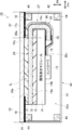
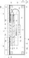
- FIG. 1 is a schematic cross-sectional view showing an example of a touch panel according to the embodiment of the present invention
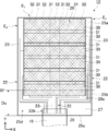
- FIG. 2 is a schematic view showing a first example of a conductive film of the touch panel according to the embodiment of the present invention
- FIG. 3 is a schematic cross-sectional view showing the configuration of the detection unit of the conductive film of the first example of the embodiment of the present invention.
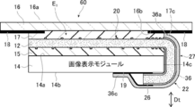
- the touch panel 10 of the first example shown in FIG. 1 has a conductive film 12, an image display module 14, a cover portion 16, a first transparent insulating layer 15, and a second transparent insulating layer 17.
- the image display module 14 the first transparent insulating layer 15, the conductive film 12, the second transparent insulating layer 17, and the cover portion 16 are laminated in this order in the stacking direction Dt.
- the conductive film 12 is arranged on the display surface 14a side of the image display module 14.
- the conductive film 12 and the image display module 14 are laminated via the first transparent insulating layer 15.
- the conductive film 12 and the cover portion 16 are laminated via a second transparent insulating layer 17.
- the first transparent insulating layer 15 is provided over the entire display surface 14a of the image display module 14.
- the first transparent insulating layer 15 and the second transparent insulating layer 17 have the same area.
- the first transparent insulating layer 15 and the second transparent insulating layer 17 have the same size when viewed from the surface 16a side of the cover portion 16.
- the first transparent insulating layer 15 arranged on the display surface 14a side of the image display module 14 so that the display object (not shown) displayed on the display surface 14a of the image display module 14 can be visually recognized, the conductive layer 15. It is preferable that the sex film 12, the second transparent insulating layer 17, and the cover portion 16 are all transparent.
- the touch panel 10 has a housing 40 that surrounds the image display module 14 and the conductive film 12.
- the image display module 14 and the conductive film 12 are housed in the interior 40a of the housing 40.
- the housing 40 has a bottom plate 41 having a shape similar to that of the cover portion 16 and a side plate 42 surrounding the outer edge of the bottom plate 41.
- cushioning materials 44 are provided at the corners of the bottom plate 41 and the side plates 42 and at the corners of the side plates 42 and the cover portion 16.
- the side plate 42 of the housing 40 is attached to the back surface 16b of the cover portion 16.
- the cushioning material 44 protects the image display module 14 and the conductive film 12 from external impacts and the like.
- the buffer material 44 can be constructed by using an ethylene-propylene sponge, a chloroprene sponge, a styrene-butadiene sponge, a nitrile rubber sponge, or the like.
- the surface 16a of the cover portion 16 is the touch surface of the touch panel 10 and serves as the operation surface.
- the touch panel 10 is input-operated using the surface 16a of the cover portion 16 as an operation surface.
- the touch surface is a surface that detects contact with a finger or a stylus pen.
- the surface 16a of the cover portion 16 serves as a visible surface of a display object (not shown) displayed on the display surface 14a of the image display module 14.
- a controller 13 is provided on the back surface 14b of the image display module 14.
- the conductive film 12 is bent so as to surround the side surface 14c of the image display module 14.
- the conductive film 12 and the controller 13 are electrically connected by a flexible wiring member such as a flexible circuit board 19.
- a decorative layer 18 having a light-shielding function is provided on the back surface 16b of the cover portion 16.
- the decorative layer 18 is provided, for example, along the outer edge of the cover portion 16 when viewed from the surface 16a side of the cover portion 16.
- the area where the decorative layer 18 is provided is the frame portion Df.
- the frame portion Df is formed by the decorative layer 18 so that the components under the frame portion Df are not visible.
- the narrow width of the frame portion Df is called a narrow frame. Narrowing the width of the frame portion Df is called narrowing the frame.
- the conductive film 12 has a bent portion 27 protruding from the first transparent insulating layer 15 and the second transparent insulating layer 17, and is in a direction orthogonal to the stacking direction Dt.
- the side surface 17c of the second transparent insulating layer 17 in Dw and the bent portion 27 of the conductive film 12 are covered with the sealing layer 36.
- the end portion 36a of the sealing layer 36 may reach the surface of the decorative layer 18 of the cover portion 16. Further, it is preferable that the end portion 36a of the sealing layer 36 is in contact with the cover portion 16 and the end portion 36c is in contact with the surface of the image display module 14 opposite to the display surface 14a, that is, the back surface 14b.
- the sealing layer 36 has such a structure, sulfurization of the conductive layer by the sealing layer 36 can be further suppressed.
- the flexible circuit board 19 is narrower than the flexible base material 25.
- the sealing layer 36 covers the flexible circuit board 19 and is provided in contact with the back surface 14b of the image display module 14.
- the sealing layer 36 the sulfurization of the electrically conductive layer of the conductive film 12 is suppressed, and suppresses the resistance change over time of the active area is an input area E 1 of the detection unit 20 of the touch panel 10.
- the sealing layer 36 is made of an electrically insulating material. For example, the degassing from the housing 40 and the buffer material 44 even sulfur gases (hydrogen sulfide gas or volatile sulfur (S 8) or the like) is generated by the sealing layer 36, the sulfur gases the conductive film 12 Infiltration into the interface with the second transparent insulating layer 17 is suppressed.
- the sealing layer 36 does not need to be configured to cover the entire surface of the conductive film 12, it is possible to suppress a decrease in the light transmittance and maintain the light transmittance.
- the input region E 1 of the detector 20 as described above, i.e., it is possible to suppress the resistance change over time of the active area. Furthermore, it is possible to achieve both narrowing the frame and maintaining the light transmittance.
- the controller 13 is composed of a known one used for detecting the touch sensor.
- the controller 13 detects the position where the capacitance is changed by the contact of a finger or the like on the surface 16a of the cover portion 16 which is the touch surface.
- the capacitance type touch panel includes a mutual capacity type touch panel and a self-capacitance type touch panel, but is not particularly limited.
- the cover portion 16 protects the conductive film 12.
- the structure of the cover portion 16 is not particularly limited.
- the cover portion 16 is preferably transparent so that a display object (not shown) displayed on the display surface 14a of the image display module 14 can be visually recognized.
- a plastic film, a plastic plate, a glass plate, or the like is used for the cover portion 16. It is preferable that the thickness of the cover portion 16 is appropriately selected according to each application.
- raw materials for the above-mentioned plastic films and plastic plates include polyesters such as polyethylene terephthalate (PET) and polyethylene naphthalate (PEN); polyethylene (PE), polypropylene (PP), polystyrene, and EVA (vinyl acetate copolymerized polyethylene).
- cover portion 16 a polarizing plate, a circular polarizing plate, or the like may be used. Since the surface 16a of the cover portion 16 is a touch surface as described above, a hard coat layer may be provided on the surface 16a if necessary.
- the thickness of the cover portion 16 is, for example, 0.1 to 1.3 mm, and particularly preferably 0.1 to 0.7 mm.
- the configuration of the first transparent insulating layer 15 is particularly limited as long as it is transparent and has electrical insulating properties, and the conductive film 12 and the image display module 14 can be stably fixed. It is not something that is done.
- an optically transparent resin OCR, Optical Clear Resin
- OCA optically transparent adhesive
- UV Ultra Violet
- the first transparent insulating layer 15 may be partially hollow.
- the second transparent insulating layer 17 is transparent and has electrical insulating properties, and if the conductive film 12 and the cover portion 16 can be stably fixed, the configuration thereof is particularly high. It is not limited.
- the second transparent insulating layer 17, the same one as that of the first transparent insulating layer 15 can be used.
- the image display module 14 includes a display surface 14a for displaying a display object such as an image, and includes, for example, a liquid crystal display device.
- the image display module 14 is not limited to the liquid crystal display device, and may be an organic EL (Organic electroluminescence) display device.
- the image display module 14 includes a cathode ray tube (CRT) display device, a vacuum fluorescent display (VFD), a plasma display panel (PDP), a surface electric field display (SED), a field emission display (FED), and an electron. Paper etc. can be used.
- the image display module 14 is appropriately used depending on its intended use, but in order to make the touch panel 10 thinner, it is preferably in the form of a panel such as a liquid crystal display panel and an organic EL panel.
- the decorative layer 18 has a light-shielding function as described above, and by covering the components such as the detection unit 20 and the take-out wiring unit 22 of the conductive film 12 under the decorative layer 18, the detection unit 18 Components such as 20 and the take-out wiring portion 22 are made invisible.
- the decorative layer 18 the configuration is not particularly limited as long as the components such as the detection unit 20 and the take-out wiring unit 22 can be made invisible, and a known decorative layer can be used.
- Various printing methods such as a screen printing method, a gravure printing method and an offset printing method, a transfer method, and a thin-film deposition method can be used for forming the decorative layer.
- the decorative layer 18 is formed on the back surface 16b of the cover portion 16, but is not limited to this, and may be formed directly on the components such as the detection portion 20 and the take-out wiring portion 22. Invisible means that the constituent under the decorative layer 18 cannot be seen, and when 10 observers see it, it means that no one can see it.
- the conductive film 12 functions as a touch sensor on the touch panel 10.
- the configuration of the conductive film 12 is not particularly limited as long as it functions as a touch sensor.
- the conductive film 12 has a detection unit 20 formed of a conductive layer on at least one surface of the transparent flexible base material 25, one end of which is electrically connected to the detection unit 20, and the other end of which is external. It has an take-out wiring portion 22 to which the connection terminal 26 is connected.
- the detection unit 20 and the take-out wiring unit 22 are provided on the front surface 25a and the back surface 25b of the flexible base material 25, respectively.
- the conductive film 12 having the flexible base material 25 is flexible and can be bent. When the conductive film 12 is polygonal, at least one side of the conductive film 12 is bent.
- the input operation is an input region E 1 which can be the person used.
- the take-out wiring portion 22 is arranged in the outer area E 2 located outside the input area E 1 .
- the sealing layer 36, sulfide in the input region E 1 of the detector 20, i.e., sulfide in the active area is suppressed, the resistance change with time of the active area can be suppressed.
- the conductive film 12 is bent at the bent position Bf determined by the design specifications and the like, and the external connection terminal 26 of the take-out wiring portion 22 is opposite to the display surface 14a side of the image display module 14. It is arranged on the side, that is, on the back surface 14b side.
- a flexible wiring member such as a flexible circuit board 19 is electrically connected to the external connection terminal 26.
- the bending position Bf of the above-mentioned conductive film 12 is the folding of the flexible base material 25. This is the planned song position.
- the flexible base material 25 is bent at the planned bending position.
- the folding position Bf of the conductive film 12 described above and the bending position of the flexible base material 25 described above are such that the conductive film 12 is incorporated in the touch panel 10 or the conductive film 12 is a single body. The difference is that they are in the same position.
- the above-mentioned bent portion 27 is a range Dc from the bent position Bf to the outer edge 25c of the flexible base material 25. That is, the bent portion 27 is a range from the bent position Bf to the end of the flexible base material 25 on the side where the detection portion 20 is not provided in the Y direction.
- An external connection terminal 26 is provided on the bent portion 27.
- the sealing layer 36 is formed in the bent portion 27, that is, the range Dc.
- the conductive film 12 shown in FIG. 2 has a configuration in which only the take-out wiring part 22 is provided out of the detection part 20 and the take-out wiring part 22 and the detection part 20 is not provided at the bent position Bf. Further, the region from the bent position Bf to the end portion 20c of the detection unit 20 is the frame region Ds corresponding to the frame portion Df.
- the detection unit 20 has, for example, a plurality of first detection electrodes 30 and a plurality of second detection electrodes 32.
- the plurality of first detection electrodes 30 are band-shaped electrodes extending in the X direction in parallel with each other, and may be electrically insulated from each other in the Y direction with an interval 31 in the Y direction orthogonal to the X direction. It is provided on the surface 25a (see FIG. 2) of the flexible base material 25.
- the plurality of second detection electrodes 32 are band-shaped electrodes extending in the Y direction in parallel with each other, and the flexible base material 25 is electrically insulated from each other in the X direction with a spacing 31 in the X direction. It is provided on the back surface 25b (see FIG. 2) of the above.
- the plurality of first detection electrodes 30 and the plurality of second detection electrodes 32 are provided at right angles, but are electrically insulated from each other by the flexible base material 25.
- the interval 31 between the first detection electrode 30 and the second detection electrode 32 is a region that is separated from the first detection electrode 30 or the second detection electrode 32 and is not electrically connected. Therefore, as described above, the plurality of first detection electrodes 30 are electrically insulated from each other in the Y direction, and the plurality of second detection electrodes 32 are electrically insulated from each other in the X direction. is there.
- the detection unit 20 is provided with six first detection electrodes 30 and five second detection electrodes 32, but the number is not particularly limited and may be a plurality.
- the first detection electrode 30 and the second detection electrode 32 are composed of, for example, a thin metal wire 33 (see FIG. 3).
- the thin metal wires 33 are arranged in a mesh pattern, for example. The pattern of the thin metal wire 33 will be described in detail later.
- Both the first detection electrode 30 and the second detection electrode 32 correspond to the conductive layer.
- the take-out wiring unit 22 is a member that plays a role of applying a voltage to the first detection electrode 30 and the second detection electrode 32.
- One end of the take-out wiring portion 22 is electrically connected to the first detection electrode 30 or the second detection electrode 32.
- An external connection terminal 26 is provided at the terminal portion 22b, which is the other end.
- the take-out wiring portion 22 may be configured by the conductive layer.
- the take-out wiring unit 22 is composed of a plurality of lead-out wirings 23. One end of each of the drawer wirings 23 is electrically connected to the first detection electrode 30 or the second detection electrode 32 described above. The other ends of the lead-out wiring 23 are collectively electrically connected to one external connection terminal 26.
- the other end of the plurality of lead-out wirings 23 is the terminal portion 22b of the take-out wiring portion 22.
- the number of outlet wirings 23 of the extraction wiring unit 22 is the same as the number of detection electrodes electrically connected.
- the take-out wiring portion 22 is electrically connected to the first detection electrode 30 at the end in the X direction, and the take-out wiring portion 22 is electrically connected to the second detection electrode 32 at one end in the Y direction. It is electrically connected, and the take-out wiring portion 22 is routed from three directions to the first detection electrode 30 and the second detection electrode 32. It is preferable that the detection unit 20 and the take-out wiring unit 22 have an integral configuration. In this case, the detection unit 20 and the take-out wiring unit 22 are formed by, for example, a lithography method.
- FIG. 14 is a schematic cross-sectional view showing a reference example of a touch panel having a conductive film
- FIG. 15 is a schematic view showing a reference example of the conductive film.
- the same components as those of the touch panel 10 shown in FIG. 1 and the conductive film 12 shown in FIG. 2 are designated by the same reference numerals, and detailed description thereof will be omitted.
- the detection unit 20 and the take-out wiring unit 22 are provided on the front surface 104a and the back surface 104b of the substrate 104, respectively, like the conductive film 102 shown in FIG.
- the outer edge 104c of the substrate 104 is the end of the substrate 104 in the Y direction on the side where the detection unit 20 is not provided.
- the external connection terminal 26 and the detection unit 20 are provided on the same surface of the substrate 104 on the front surface 104a or on the same surface of the back surface 104b.
- the flexible circuit board 19 is electrically connected to the external connection terminal 26 provided at the terminal portion 22b of the take-out wiring portion 22.
- the conductive film 102 shown in FIG. 15 has a configuration in which the flexible circuit board 19 is bent without bending the conductive film 102.
- the flexible circuit board 19 has a bent position Bf, and the flexible circuit board 19 is bent at the bent position Bf and electrically connected to the controller 13 as shown in FIG.
- the sealing layer 36 (see FIG. 14) is formed in the region 105 from the end 20c of the detection unit 20 to the outer edge 104c of the substrate 104.
- the sealing layer 36 allows the sulfur gas to be secondly transparently insulated from the conductive film 12. Infiltration into the interface with the layer 17 cannot be suppressed. Therefore, the sulfurization of the conductive layer of the conductive film 102 cannot be suppressed, and the conductive layer is sulfurized due to the infiltration of sulfur gas.
- the electrical resistance of the conductive layer increases due to sulfurization, and the resistance changes over time in the active area.
- the conductive layer may be colored due to sulfurization, and the appearance of the conductive layer may be deteriorated, so that the conductive layer may be visually recognized.
- the curvature of the bent portion becomes larger than when the conductive film 12 (see FIG. 2) is bent. From this, it is not possible to realize a narrow frame.
- the conductive film 12 shown in FIG. 2 has flexibility, and the conductive film 12 itself can be bent. Therefore, as compared with the case where the flexible circuit board 19 is bent like the conductive film 102 shown in FIG. 15, the conductive film 12 shown in FIG. 2 can have a smaller bending curvature, whereby the touch panel 10 (FIG. (See 1) can be narrowed.
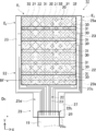
- FIG. 4 is a schematic view showing a second example of the conductive film of the touch panel according to the embodiment of the present invention.
- the conductive film 12 of the second example shown in FIG. 4 is different from the conductive film 12 shown in FIG. 2 in that the bending position Bf of the conductive film 12 is different from that of the take-out wiring portion 22. Since the configuration is the same as that of the conductive film 12 shown in FIG. 2 except that the space 25d between the flexible base material 25 and the outer edge 25c is narrow, detailed description thereof will be omitted.
- the frame region Ds can be made substantially zero, and a narrower frame can be realized.
- the width of the decorative layer 18 can be reduced, resulting in a narrower frame.
- the width of the decorative layer 18 is narrower than that of the touch panel 10 shown in FIG. 1, and the frame portion Df can be made into a narrower frame. ..
- the structure of the conductive film 12 is not limited to the above. For example, the configuration shown in FIGS. 5 to 7 may be used.
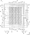
- FIG. 5 is a schematic view showing a third example of the conductive film of the touch panel according to the embodiment of the present invention
- FIG. 6 is a schematic view showing a fourth example of the conductive film of the touch panel according to the embodiment of the present invention
- FIG. 7 is a schematic view showing a fifth example of the conductive film of the touch panel according to the embodiment of the present invention.
- the same components as those of the conductive film 12 shown in FIG. 2 are designated by the same reference numerals, and detailed description thereof will be omitted.
- the same components as those of the conductive film 12 shown in FIG. 5 are designated by the same reference numerals, and detailed description thereof will be omitted.
- the conductive film 12 shown in FIG. 5 has a configuration other than the point where the flexible base material 25 has a band-shaped projecting portion 29, except that the conductive film 12 shown in FIG. Since it is the same as 12, the detailed description thereof will be omitted.
- the protruding portion 29 is provided with a take-out wiring portion 22, and the protruding portion 29 has a terminal portion 22b of the take-out wiring portion 22.
- the flexible circuit board 19 is electrically connected to the external connection terminal 26 provided at the terminal portion 22b.
- the bent position Bf is at the protruding portion 29.
- the protruding portion 29 can be formed by punching out or partially cutting the flexible base material 25.
- the sealing layer 36 (FIG. 1) is formed in the range Dc from the bent position Bf to the outer edge 25c of the flexible base material 25, that is, the bent portion 27 composed of the protruding portion 29 (FIG. 1). See) is formed.
- the position of the protruding portion 29 is set to the center in the X direction in the conductive film 12 shown in FIG. 5, but the position is not limited to this.
- the position of the protruding portion 29 is appropriately determined according to the layout of the detecting portion 20 and the taking-out wiring portion 22 and the like. Further, depending on the size of the detection unit 20, a plurality of portions connected to the flexible circuit board 19 may be provided. In this case, the number of protruding portions 29 is the same as the number of portions connected to the flexible circuit board 19. Therefore, the number of the protruding portions 29 is not limited to one, and may be a plurality. The plurality of protruding portions 29 can be bent.
- the conductive film 12 shown in FIG. 6 has the same configuration as the conductive film 12 shown in FIG. 5 except that the bending position Bf is different from that of the conductive film 12 shown in FIG. Detailed description will be omitted. Similar to the conductive film 12 shown in FIG. 4 above, the conductive film 12 shown in FIG. 6 has a detection unit 20 and a take-out wiring part 22 at the bent position Bf, and the detection part 20 and the take-out wiring part 22 are provided. Can be folded. As shown in FIG. 6, in the conductive film 12, the frame region Ds can be made substantially zero by bending the conductive film 12 at the bending position Bf where the detection unit 20 is located, and a narrower frame can be realized.
- the width of the decorative layer 18 can be reduced, and a touch panel with a narrower frame can be obtained.
- the conductive film 12 shown in FIG. 6 is composed of a range Dc from the bent position Bf to the outer edge 25c of the flexible base material 25, that is, a part of the flexible base material 25 and a protruding portion 29.
- a sealing layer 36 is formed on the bent portion 27 to be formed.
- the number of the first detection electrodes 30, the number of the second detection electrodes 32, and the take-out wiring portion 22 are pulled out in two directions as compared with the conductive film 12 shown in FIG. Since the other configurations are the same as those of the conductive film 12 shown in FIG. 2, detailed description thereof will be omitted.
- the take-out wiring portion 22 is pulled out from each of the outer edges 25c on both sides in the Y direction where the first detection electrode 30 of the flexible base material 25 extends, and the take-out wiring portion 22
- An external connection terminal 26 is provided at the terminal portion 22b of the above.
- the flexible circuit board 19 is electrically connected to the external connection terminal 26.
- the pull-out direction of the take-out wiring portion 22 is not limited to that shown in FIG. 7.
- the bending position Bf is provided at two points and can be bent at two points.
- the bent position Bf has a configuration in which only the extraction wiring unit 22 is present and the detection unit 20 is not included in the detection unit 20 and the extraction wiring unit 22, but the present invention is not limited to this, and the detection unit 20 and the extraction wiring are not limited to this.
- the conductive film 12 is configured to be bent at two points, but the present invention is not limited to this, and the conductive film 12 may be bent at one point.
- the flexible base material 25 may be bent at the take-out wiring portion 22 of the outer region E 2 in the X direction.
- the conductive film 12 shown in FIG. 7 can be bent at a maximum of four points.
- FIG. 8 is a schematic view showing the electrode configuration of the detection unit of the conductive film of the touch panel according to the embodiment of the present invention
- FIG. 9 shows the shape of the mesh pattern of the detection unit of the conductive film of the touch panel according to the embodiment of the present invention.
- the first detection electrode 30 and the second detection electrode 32 of the detection unit 20 are composed of the thin metal wire 33 as described above.
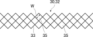
- the first detection electrode 30 and the second detection electrode 32 have, for example, as shown in FIG. 8, a mesh pattern in which a plurality of thin metal wires 33 intersect.
- the drawer wiring 23 can also have the same configuration as the first detection electrode 30 and the second detection electrode 32.
- the leader wiring 23 may have a mesh pattern in which a plurality of thin metal wires 33 intersect.
- the mesh pattern pattern is not particularly limited, and a triangle such as an equilateral triangle, an isosceles triangle, or a right-angled triangle, or a quadrangle. , Rectangle, rhombus, parallelogram, trapezoidal quadrangle, (regular) hexagon, (regular) octagonal (regular) n-sided, circle, ellipse, star, etc. preferable.
- the mesh of the mesh pattern is intended to have a shape including a plurality of openings 35 composed of intersecting thin metal wires 33.
- the opening 35 is an opening region surrounded by a thin metal wire 33.
- the upper limit of the length W of one side of the opening 35 is preferably 800 ⁇ m or less, more preferably 600 ⁇ m or less, further preferably 400 ⁇ m or less, and the lower limit is preferably 5 ⁇ m or more, more preferably 30 ⁇ m or more, still more preferably 80 ⁇ m or more.
- the conductive film 12 see FIG. 1 can be used with the image display module 14 (see FIG. 1).
- the display can be visually recognized without discomfort.
- the aperture ratio of the mesh pattern is preferably 85% or more, more preferably 90% or more, and further preferably 95% or more.
- the aperture ratio corresponds to the transmissive portion excluding the thin metal wire in the region provided with the conductive layer, that is, the ratio of the opening portion to the entire region provided with the conductive layer.
- the configuration of the detection unit 20 is limited to a configuration in which the first detection electrode 30 is provided on the front surface 25a of the flexible base material 25 and the second detection electrode 32 is provided on the back surface 25b. is not.
- the first detection electrode 30 and the second detection electrode 32 may be provided on separate flexible substrates and laminated.
- the flexible base material 25 provided with the first detection electrode 30 and the flexible base material 25 provided with the second detection electrode 32 are transparent and electrically insulated insulators. It may be a structure in which layers are laminated. The structure is not limited to the configuration in which the detection unit 20 is provided on the front surface 25a and the back surface 25b of the flexible base material 25, respectively. As shown in FIG.
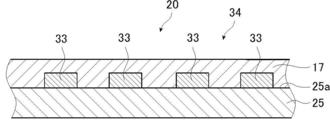
- the detection electrode 34 may be provided only on one surface of the flexible base material 25, for example, only on the surface 25a.
- the detection electrode 34 shown in FIG. 10 functions as the detection unit 20.
- the detection electrode 34 is composed of a plurality of thin metal wires 33 like the first detection electrode 30 (see FIG. 8), and the thin metal wires 33 are provided on the surface 25a.
- FIG. 10 is a schematic cross-sectional view showing an example of the configuration of the detection unit of the conductive film of the touch panel according to the embodiment of the present invention.
- the first detection electrode 30 and the second detection electrode 32 of the detection unit 20 are formed of conductive fibers such as silver nanowires, carbon nanotubes (CNT), and carbon nanobuds (CNB). It may be a combination of these.
- the flexible base material means that it can be bent, and specifically, it means that it does not crack even if it is bent with a radius of curvature of 1 mm.
- the flexible base material supports the detection portion and the take-out wiring portion, and is a flexible support.
- the type of the flexible base material is not limited as long as it can support the detection portion and the take-out wiring portion and has flexibility, and a transparent support is preferable.
- a plastic sheet is preferred.
- Specific examples of the materials constituting the flexible substrate include PET (polyethylene terephthalate) (258 ° C.), polycycloolefin (134 ° C.), polycarbonate (250 ° C.), (meth) acrylic resin (128 ° C.), and PEN.
- Polyethylene terephthalate (269 ° C), PE (polyethylene) (135 ° C), PP (polypropylene) (163 ° C), polystyrene (230 ° C), polyvinyl chloride (180 ° C), polyvinylidene chloride (212 ° C), PolyPVDF (vinylidene fluoride) (177 ° C), PAR (polyarylate) (250 ° C), PES (polyethersulfon) (225 ° C), high molecular weight acrylic resin, fluorene derivative (140 ° C), crystalline COP ( A plastic film having a melting point of about 290 ° C.
- the value in parentheses is the melting point or the glass transition temperature.
- the total light transmittance of the flexible substrate is preferably 85 to 100%.
- the thickness of the flexible base material is not particularly limited, but from the viewpoint of application to a touch panel, it can usually be arbitrarily selected in the range of 25 to 500 ⁇ m. When the function of the touch surface is also used in addition to the function of the flexible base material, it is possible to design with a thickness exceeding 500 ⁇ m.
- One preferred embodiment of the flexible substrate is a treated support that has been subjected to at least one treatment selected from the group consisting of atmospheric pressure plasma treatment, corona discharge treatment, and ultraviolet irradiation treatment.
- at least one treatment selected from the group consisting of atmospheric pressure plasma treatment, corona discharge treatment, and ultraviolet irradiation treatment.
- a configuration having an undercoat layer containing a polymer on the surface thereof may be used.
- the method for forming the undercoat layer is not particularly limited, and examples thereof include a method in which a composition for forming an undercoat layer containing a polymer is applied onto a flexible substrate and heat treatment is performed as necessary.
- the undercoat layer forming composition may contain a solvent, if necessary.
- the type of solvent is not particularly limited, and known solvents are exemplified.
- a latex containing fine particles of the polymer may be used as a composition for forming an undercoat layer containing a polymer.
- the thickness of the undercoat layer is not particularly limited, but is preferably 0.02 to 0.3 ⁇ m, more preferably 0.03 to 0.2 ⁇ m, in that the adhesion between the detection portion and the take-out wiring portion is more excellent.
- the line width of the thin metal wire constituting the detection unit and the take-out wiring unit is not particularly limited, but the upper limit is preferably 30 ⁇ m or less, more preferably 15 ⁇ m or less, further preferably 10 ⁇ m or less, particularly preferably 9 ⁇ m or less, and most preferably 7 ⁇ m or less.
- the lower limit is preferably 0.5 ⁇ m or more, more preferably 1.0 ⁇ m or more. Within the above range, low resistance electrodes can be formed relatively easily.
- the line width of the thin metal wire is preferably 500 ⁇ m or less, more preferably 50 ⁇ m or less, still more preferably 30 ⁇ m or less. Within the above range, a touch panel electrode having low resistance can be formed relatively easily.
- the thickness of the thin metal wire is not particularly limited, but is preferably 0.01 to 200 ⁇ m, more preferably 30 ⁇ m or less, further preferably 20 ⁇ m or less, particularly preferably 0.01 to 9 ⁇ m, and 0. Most preferably, it is 05 to 5 ⁇ m. Within the above range, it is relatively easy to form an electrode having excellent durability with a low resistance electrode.
- the material of the fine metal wire examples include metals or alloys such as gold (Au), silver (Ag), molybdenum (Mo), copper (Cu), titanium (Ti), aluminum (Al) and tungsten (W). Can be mentioned. Of these, silver is preferable because of the excellent conductivity of the thin metal wire. It is preferable that the fine metal wire contains a binder from the viewpoint of adhesion between the fine metal wire and the flexible base material. As the binder, a resin is preferable because the adhesion between the fine metal wire and the flexible base material is more excellent, and more specifically, a (meth) acrylic resin, a styrene resin, a vinyl resin, and a polyolefin resin.
- a binder a resin is preferable because the adhesion between the fine metal wire and the flexible base material is more excellent, and more specifically, a (meth) acrylic resin, a styrene resin, a vinyl resin, and a polyolefin resin.
- Polyester resin Polyurethane resin, Polyamide resin, Polycarbonate resin, Polydiene resin, Epoxy resin, Silicone resin, Cellulosic polymer, Chitosan polymer, at least one resin selected from the group.
- a copolymer composed of monomers constituting these resins can be mentioned.
- the thin metal wire containing the binder will be described in detail later.
- the method for producing the thin metal wire is not particularly limited, and a known method can be adopted.
- a method of exposing and developing a photoresist film on a metal foil formed on the surface of a flexible base material to form a resist pattern and etching the metal foil exposed from the resist pattern can be mentioned.
- a method of printing a paste containing metal fine particles or metal nanowires on both main surfaces of a flexible base material and performing metal plating on the paste can be mentioned.
- Another method is to form a patterned groove structure on the surface of the flexible base material in advance and embed a paste containing metal fine particles or metal nanowires in the grooves by screen printing.
- a method of forming a fine metal wire by pattern printing an ink containing metal fine particles or metal nanowires on the surface of a flexible base material by an inkjet method can be mentioned.
- a method using silver halide can be mentioned. More specifically, the methods described in paragraphs 0056 to 0114 of JP-A-2014-209332 can be mentioned. The method using silver halide will be described in detail later.
- a preferred form of the detection unit includes an embodiment including a mesh pattern made of fine silver wires, in which the first detection electrode is arranged on the front surface of the above-mentioned flexible base material and the second detection electrode is arranged on the back surface. preferable.
- the first detection electrode 30 and the second detection electrode 32 of the detection unit 20, and the extraction wiring 23 of the extraction wiring unit 22 are not limited to being composed of a thin metal wire, and are dispersed in the binder and the binder. It can also be composed of a conductive wire containing a metal portion.
- the above-mentioned binder contains a first polymer and a second polymer having a glass transition temperature lower than that of the first polymer.
- the glass transition temperature of the polymer means the glass transition temperature measured by the differential scanning calorimetry (DSC) method. The glass transition temperature is measured by using the "plastic transition temperature measuring method" specified in JIS K7121 (2012).
- first polymer and the second polymer examples include hydrophobic polymers (hydrophobic resins), and more specifically, acrylic resins, styrene resins, vinyl resins, polyolefin resins, and polyesters. At least one resin selected from the group consisting of based resins, polyurethane resins, polyamide resins, polycarbonate resins, polydiene resins, epoxy resins, silicone resins, cellulose polymers and chitosan polymers, or , Copolymers composed of monomers constituting these resins and the like.
- the polymer preferably contains a reactive group that reacts with a cross-linking agent described later.
- the polymer preferably has at least one unit selected from the group consisting of the following formulas A, B, C, and D.
- a polymer consisting of one unit selected from the group consisting of formulas A, B, C, and D is preferable from the viewpoint of lowering the glass transition temperature and making it easier to control.
- a polymer consisting of at least one unit selected from the group consisting of, C, and D is more preferable, and a polymer consisting of a unit represented by the formula D is further preferable.
- R 1 represents a methyl group or a halogen atom, preferably a methyl group, a chlorine atom or a bromine atom.
- p represents an integer of 0 to 2, preferably 0 or 1, more preferably 0.
- R 2 represents a methyl group or an ethyl group, and a methyl group is preferable.
- R 3 represents a hydrogen atom or a methyl group, and a hydrogen atom is preferable.
- L represents a divalent linking group, and a group represented by the following general formula (2) is preferable.
- R 30 represents a hydrogen atom, an alkyl group, an aryl group, or an acyl group, and may each have a substituent (for example, a halogen atom, a nitro group, a hydroxyl group, etc.).
- R 30 is preferably a hydrogen atom, an alkyl group having 1 to 10 carbon atoms (for example, a methyl group, an ethyl group, an n-butyl group, an n-octyl group, etc.), an acyl group (for example, an acetyl group, a benzoyl group, etc.).
- X 1 is an oxygen atom or NH-.
- X 2 represents an alkylene group, an arylene group, an alkylene arylene group, an arylene alkylene group, or an alkylene arylene alkylene group, and these groups include -O-, -S-, -OCO-, -CO-, and -COO.
- R 31 represents a linear or branched alkyl group having 1 to 6 carbon atoms, and includes a methyl group, an ethyl group, an isopropyl group and the like.
- Preferred examples of X 2 are dimethylene group, trimethylene group, tetramethylene group, o-phenylene group, m-phenylene group, p-phenylene group, -CH 2 CH 2 OCOCH 2 CH 2- , and -CH 2 CH 2 OCO (C 6 H 4 )-etc.
- r represents 0 or 1.
- q represents 0 or 1, preferably 0.
- R 4 represents an alkyl group having 1 to 80 carbon atoms, an alkenyl group, or an alkynyl group.
- the first polymer is preferably an alkyl group having 1 to 5 carbon atoms
- the second polymer is preferably an alkyl group having 1 to 5 carbon atoms.
- An alkyl group having 5 to 50 carbon atoms is preferable, an alkyl group having 5 to 30 carbon atoms is more preferable, and an alkyl group having 5 to 20 carbon atoms is further preferable.
- R 5 is a hydrogen atom, a methyl group, an ethyl group, a halogen atom, or a -CH 2 COOR 6
- a hydrogen atom, a methyl group, a halogen atom or a -CH 2 COOR 6 is preferably a hydrogen atom, a methyl group , Or -CH 2 COOR 6 is more preferred, and a hydrogen atom is particularly preferred.
- R 6 represents a hydrogen atom or an alkyl group having 1 to 80 carbon atoms, and may be the same as or different from R 4, and the carbon number of R 6 is preferably 1 to 70, more preferably 1 to 60.
- a polymer (copolymer) represented by the following general formula (1) can be mentioned from the viewpoint of being able to further prevent the infiltration of water.
- A, B, C, and D have already been described. Represents the repeating unit described above.
- x, y, z, and w represent the molar ratio of each repeating unit.
- x is 3 to 60 mol%, preferably 3 to 50 mol%, and more preferably 3 to 40 mol%.
- the y is 30 to 96 mol%, preferably 35 to 95 mol%, and more preferably 40 to 90 mol%.
- the z is 0.5 to 25 mol%, preferably 0.5 to 20 mol%, and more preferably 1 to 20 mol%.
- w is 0.5 to 40 mol%, preferably 0.5 to 30 mol%.
- it is particularly preferable that x is 3 to 40 mol%, y is 40 to 90 mol%, z is 0.5 to 20 mol%, and w is 0.5 to 10 mol%.
- the polymers represented by the general formula (1) the polymers represented by the following general formulas (2) and (3) are preferable.
- x, y, z and w are as defined above.
- a1, b1, c1, d1, and e1 represent the molar ratio of each monomer unit, a1 is 3 to 60 (mol%), b1 is 30 to 95 (mol%), and c1 is 0.5. ⁇ 25 (mol%), d1 represents 0.5-40 (mol%), and e1 represents 1-10 (mol%).
- the preferred range of a1 is the same as the preferred range of x described above, the preferred range of b1 is the same as the preferred range of y described above, the preferred range of c1 is the same as the preferred range of z described above, and d1
- the preferred range is the same as the preferred range of w described above.
- e1 is 1 to 10 mol%, preferably 2 to 9 mol%, and more preferably 2 to 8 mol%.
- the weight average molecular weight of the polymer represented by the general formula (1) is preferably 10 to 1,000,000, more preferably 2000 to 750,000, and even more preferably 3000 to 500,000.
- the polymer represented by the general formula (1) can be synthesized by referring to, for example, Japanese Patent No. 3305459 and Japanese Patent No. 3754745.
- the glass transition temperature of the first polymer and the second polymer is not particularly limited, but the glass transition temperature of the first polymer is preferably 0 ° C. or higher, more preferably 25 ° C. or higher. It is more preferable to exceed 40 ° C.
- the upper limit is not particularly limited, but is generally preferably 120 ° C. or lower.
- the glass transition temperature of the second polymer is not particularly limited, but is preferably 40 ° C. or lower, more preferably 25 ° C. or lower, further preferably less than 25 ° C., particularly preferably 0 ° C. or lower, and 0 ° C. Less than is most preferred.
- the lower limit is not particularly limited, but is generally preferably ⁇ 50 ° C. or higher.
- the difference (absolute value) between the glass transition temperature of the first polymer and the glass transition temperature of the second polymer is not particularly limited, but is generally preferably 20 to 100 ° C.
- the metal portion of the conductive wire is a portion that guarantees the conductive characteristics of the conductive wire, and the metal portion is made of metal.
- the metal constituting the metal part is a group consisting of gold (metal gold), silver (metal silver), copper (metal copper), nickel (metal nickel), and palladium (metal palladium) in that the conductive properties are more excellent. At least one metal more selected is preferred.
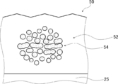
- FIG. 11 is an enlarged view of the conductive wire 50.
- FIG. 11 shows a form in which the metal portion 54 is formed into particles and dispersed in the conductive wire 50, but the form of the metal portion 54 is not limited to the particle shape, and the metal portion 54 is layered ( (Not shown) may be formed and dispersed in the conductive wire 50.
- the conductive wire 50 shown in FIG. 11 includes a binder 52 containing a first polymer and a second polymer, and a plurality of metal portions 54 dispersed in the binder 52.
- the metal portion 54 is in the form of
- the conductive wire may contain a material other than those described above.
- materials other than those described above include non-metal fine particles.
- non-metal fine particles include resin particles and metal oxide particles, and metal oxide particles are preferable.
- metal oxide particles include silicon oxide particles and titanium oxide particles.
- the average particle size of the non-metal fine particles is not particularly limited, but the equivalent sphere diameter is preferably 1 to 1000 nm, more preferably 10 to 500 nm, and even more preferably 20 to 200 nm. Within the above range, the detection unit tends to have more excellent transparency and more excellent conductivity.
- the sphere-equivalent diameter of the non-metal fine particles is obtained by calculating the sphere-equivalent diameter of any 50 particles using a transmission electron microscope and arithmetically averaging them.
- the conductive wire preferably has a metal stabilizer on the surface or inside of the metal portion or in the binder for the purpose of stabilizing the metal portion.
- the metal stabilizer the following materials can be used alone or in combination.
- Corrosion inhibitors according to Japanese Patent Application Laid-Open No. 2009-505358, paragraphs 0075 to 0086.
- Metal ion trapping agents described in JP-A-2009-188360, paragraphs 0077-0092.
- Japanese Patent Application Laid-Open No. 2014-0751115, paragraphs 0030 to 0066 Compounds for forming a silver ion diffusion inhibitory layer.
- Anticorrosive agents described in JP-A-2018-024784, paragraphs 0050 to 0057.
- the mercaptobenzothiazoles described in JP-A-2019-016488, paragraphs 0050 to 0057.
- metal stabilizer a specific compound described later can be preferably used.
- the following compounds or salts thereof are preferable as the metal stabilizer.
- a compound having a mercaptothiazole skeleton or a mercaptothiadiazole skeleton, or a compound selected from salts thereof is particularly effective for improving sulfurization resistance and is most preferable.
- the most preferable compounds include 2-mercaptobenzothiazole, 5-methyl-2-mercaptobenzothiazole, 2-amino-5-mercapto-1,3,4-thiadiazole, and 2-mercapto-5-methylthio-1. , 3,4-Thiadiazole, 2-mercapto-5-ethylthio-1,3,4-thiadiazole, 2-5-dimercapto-1,3,4-thiadiazole and derivatives or salts thereof.
- the introduction of the metal stabilizer is useful for improving the durability of the metal material in the bent portion and the non-folded portion, and particularly when silver is used for the metal portion, it is effective in suppressing migration and sulfurization, which is preferable.
- a method of introducing the metal stabilizer a method of applying a conductive film to a solution containing the metal stabilizers or contacting them by immersion during or after the formation of the conductive wire, or a method of fumigating these metal stabilizers.
- a method of depositing on a conductive film by a vapor phase reaction or the like can be preferably used. It is also preferable that the metal stabilizer is contained in the above-mentioned transparent insulating layer.
- the metal stabilizer in the transparent insulating layer in advance, it is not necessary to contact the conductive wire with the solvent required to dissolve the metal stabilizer, and damage to the conductive wire or the binder due to the solvent is avoided. It is preferable. Therefore, it is preferable that at least one of the first transparent insulating layer and the second transparent insulating layer contains a metal stabilizer. Further, the resistance change with time in the active area is an input area E 1 of the detection unit 20 of the touch panel 10 is likely to be generated in the touch panel of the configuration is no bent portion. However, since at least one of the first transparent insulating layer and the second transparent insulating layer contains a metal stabilizer, it is possible to suppress the resistance change even in the above-mentioned touch panel having no bent portion. ..
- the amount of these metal stabilizers used is not limited, but at least one of the transparent insulating layer and the conductive film may be contained in the range of 1 mg / m 2 to 10 g / m 2 per conductive layer. It is preferably contained in the range of 10 mg / m 2 to 1 g / m 2 , and more preferably.
- the shape of the conductive wire is not particularly limited, but it may be linear (straight line, curved line, or a combination thereof, etc.) so that better touch position detection performance can be obtained when applied to a touch panel. It is preferable to have it.
- the line width of the conductive wire is not particularly limited, but is preferably 30 ⁇ m or less, more preferably 15 ⁇ m or less, still more preferably 10 ⁇ m or less, from the viewpoint of the balance between the conductive characteristics of the conductive wire and the difficulty in visual recognition. It is particularly preferably 5 ⁇ m or less, most preferably 4 ⁇ m or less, preferably 0.5 ⁇ m or more, and more preferably 1.0 ⁇ m or more.
- the thickness of the conductive wire is not particularly limited, but is preferably 200 ⁇ m or less, more preferably 30 ⁇ m or less, further preferably 10 ⁇ m or less, and 0.3 to 5 ⁇ m in terms of the balance between thinning and conductive characteristics. Is particularly preferable, and 0.5 to 5 ⁇ m is most preferable.
- the method of manufacturing the detection unit will be described by taking the case where the metal portion of the conductive wire contains silver (metal silver) as an example. A method having the following steps is preferable in that more excellent productivity can be obtained.
- ⁇ Process A A silver halide-containing coating solution containing at least silver halide and a first polymer and a composition-adjusting coating solution containing at least a second polymer are simultaneously coated on a flexible base material in multiple layers.
- ⁇ Process B A step of exposing a silver halide photosensitive layer and then developing it to form a conductive wire containing metallic silver. In the following, each step will be described in detail.
- step A a silver halide-containing coating solution containing at least silver halide and a first polymer and a composition-adjusting coating solution containing at least a second polymer are simultaneously layered on a flexible substrate.
- This is a step of coating to form a silver halide photosensitive layer.
- the stacking order of each coating liquid in the case of simultaneous layer coating is not particularly limited.
- the silver halide-containing coating liquid and the composition-adjusting coating liquid may be laminated in this order from the flexible substrate side.
- the composition-adjusting coating liquid and the silver halide-containing coating liquid may be laminated in this order from the flexible substrate side.
- the composition-adjusting coating liquid, the silver halide-containing coating liquid, and the composition-adjusting coating liquid may be laminated in this order.
- coating on a flexible base material means that the coating is applied directly on the surface of the flexible base material or that a separate layer is arranged on the flexible base material and is applied on the layer. Also include.
- this step since the silver halide-containing coating liquid containing silver halide and the composition-adjusting coating liquid not containing silver halide are simultaneously coated in multiple layers, a two-layer coating film formed from both coating liquids is applied. Diffusion of the components proceeds at the interface of. More specifically, a coating film formed from a composition-adjusting coating film from a coating film formed from a silver halide-containing coating film (hereinafter, also referred to as coating film A) arranged on a flexible substrate.
- coating film A a coating film formed from a composition-adjusting coating film from a coating film formed from a silver halide-containing coating film (hereinafter, also referred to as coating film A) arranged on a flexible substrate.
- Diffusion of a part of silver halide and the first polymer proceeds in (hereinafter, also referred to as coating film B).
- the region on the coating film A side in the coating film B contains silver halide and the first polymer, and the content thereof is the silver halide and the first polymer in the coating film A. Less than the content of.
- region w Since the region on the coating film A side (hereinafter, also referred to as “region w”) in the coating film B contains silver halide transferred from the coating film A, this region w is subjected to the step B described later. Will form an upper region in the conductive wire.
- the content-mass ratio of the content of the second polymer to the total content of the content of the first polymer and the content of the second polymer becomes larger than that in the intermediate region. Cheap.
- the silver halide-containing coating liquid may contain at least silver halide and the first polymer, and may further contain the second polymer.
- the content of the first polymer in the silver halide-containing coating liquid and the content-mass ratio of the second polymer to the content of the second polymer are the contents of the first polymer in the composition-adjusting coating liquid. And it is preferably smaller than the content mass ratio of the second polymer to the content of the second polymer.
- the composition-adjusting coating liquid may contain at least the second polymer, and may further contain silver halide and / or the first polymer.
- the content thereof is not particularly limited, but the content of silver halide in the silver halide-containing coating liquid is determined in the composition-adjusting coating liquid. It is preferable that the content of silver halide is lower. By doing so, it is easy to obtain a detection unit having less reflection of external light.
- the composition-adjusting coating liquid further contains the first polymer
- the content of the first polymer and the content mass ratio of the first polymer to the content of the second polymer in the composition-adjusting coating liquid are determined to be silver halide. It is preferably smaller than the content of the first polymer and the content of the first polymer to the content of the second polymer in the coating liquid.
- the silver halide contained in the silver halide-containing coating liquid is not particularly limited, and known silver halide can be used.
- the halogen element contained in silver halide may be any of chlorine, bromine, iodine and fluorine, and these may be combined.
- silver chloride, silver bromide, or silver halide mainly composed of silver iodide is preferably used, and silver bromide or silver halide mainly composed of silver chloride is preferably used.
- Silver bromide, silver iodide bromide, or silver bromide is also preferably used.
- silver bromide More preferably, it is silver bromide, silver bromide, silver iodide bromide, or silver bromide, and most preferably silver bromide or iodide salt containing 50 mol% or more of silver chloride.
- Silver bromide is used.
- the "silver halide mainly composed of silver bromide” refers to silver halide having a molar fraction of bromide ions in the silver halide composition of 50% or more.
- the silver halide particles mainly composed of silver bromide may contain iodide ions and chloride ions in addition to bromide ions.
- the silver halide is in the form of solid particles, and the average particle size of silver halide is preferably 0.1 to 1000 nm (1 ⁇ m) in equivalent diameter of a sphere, more preferably 0.1 to 300 nm. It is more preferably about 200 nm.
- the spherical equivalent diameter of the silver halide particles is the diameter of particles having the same volume and having a spherical particle shape.
- the shape of the silver halide particles is not particularly limited, and may be various, for example, spherical, cubic, flat plate (hexagonal flat plate, triangular flat plate, tetragonal flat plate, etc.), octahedron, tetradecahedron, etc. Can be in shape.
- metal compounds belonging to Group VIII and Group VIIB such as rhodium compounds and iridium compounds and palladium compounds used for stabilizing or sensitizing silver halide
- paragraph 0039 of JP2009-188360A paragraph 0039 of JP2009-188360A.
- the description in paragraph 0042 can be referred to.
- the technical description in paragraph 0043 of JP2009-188360A can be referred to.
- the first polymer contained in the silver halide-containing coating liquid and sometimes contained in the composition-adjusting coating liquid and the first polymer contained in the composition-adjusting coating liquid and sometimes contained in the silver halide-containing coating liquid. 2 Since the form of the polymer is as described above, the description thereof will be omitted.
- the silver halide-containing coating liquid and the composition-adjusting coating liquid may contain components other than silver halide, the first polymer, and the second polymer, and these components are the silver halide-containing coating. It is common to the liquid and the composition-adjusting coating liquid, and is as described below.
- the silver halide-containing coating liquid and the composition-adjusting coating liquid may further contain gelatin.
- the type of gelatin is not particularly limited, and for example, acid-treated gelatin may be used in addition to lime-treated gelatin, and a hydrolyzate of gelatin, a gelatin enzymatic decomposition product, and an amino group or a carboxyl group are modified.
- Gelatin phthalated gelatin, acetylated gelatin
- the silver halide-containing coating liquid and the composition-adjusting coating liquid may further contain a solvent.
- a solvent examples include water, organic solvents (for example, alcohols such as methanol, ketones such as acetone, amides such as formamide, sulfoxides such as dimethyl sulfoxide, esters such as ethyl acetate, and ethers. Etc.), ionic liquids, and mixed solvents thereof.
- the silver halide-containing coating liquid and the composition-adjusting coating liquid may contain materials other than those described above.
- a cross-linking agent used for cross-linking the above-mentioned first polymer and second polymer.
- the inclusion of the cross-linking agent promotes cross-linking between the polymers, and even when gelatin is decomposed and removed in the step described later, the connection between the metallic silver is maintained, and as a result, the conductive properties are more excellent.
- the method of simultaneously coating the silver halide-containing coating liquid and the composition-adjusting coating liquid in multiple layers is not particularly limited, and a known method can be adopted.
- a die coating method is preferably used.
- the die coating method includes a slide coating method, an extrusion coating method, and a curtain coating method.
- the slide coating method or the extrusion coating is preferable, and the extrusion coating having high thin layer coating suitability is most preferable.
- the film (surface film) formed when the above-mentioned conductive film for a touch panel is applied on a predetermined substrate is easy to obtain. It is preferable to use a composition-adjusting coating liquid containing a second polymer having a composition such that the dry thickness of the coating film is 300 nm or more.
- the obtained coating film may be subjected to a drying treatment, if necessary.
- a drying treatment By carrying out the drying treatment, the solvent contained in the coating film obtained from the silver halide-containing coating solution and the coating film obtained from the composition-adjusting coating solution can be easily removed.
- a photosensitive layer containing silver halide can be formed on the flexible substrate.
- the above-mentioned "photosensitive layer containing silver halide” may be referred to as “silver halide photosensitive layer” or simply "photosensitive layer”.
- Step B is a step of exposing the silver halide photosensitive layer and then developing it to form a conductive wire containing metallic silver.
- silver halide is reduced to form a conductive wire containing metallic silver.
- the exposure process is performed in a pattern, and a conductive wire containing metallic silver is formed in the exposed portion.
- silver halide is eluted by the development process described later.
- a non-conductive wire containing the above-mentioned gelatin and the above-mentioned polymer is formed.
- the non-conductive wire is substantially free of metallic silver, and the non-conductive wire is intended as a region that does not exhibit conductivity.
- the exposure process is a process of exposing the photosensitive layer.
- silver halide in the photosensitive layer in the exposed region forms a latent image.
- a conductive wire is formed by a development process described later.
- the silver halide dissolves and flows out from the photosensitive layer during the development treatment described later, and a transparent film (non-conductive wire) is obtained.
- the light source used at the time of exposure is not particularly limited, and examples thereof include visible light, light such as ultraviolet rays, and radiation such as X-rays.
- the method of performing pattern exposure is not particularly limited, and for example, surface exposure using a photomask may be used, or scanning exposure using a laser beam may be used.
- the shape of the pattern is not particularly limited, and is appropriately adjusted according to the pattern of the conductive wire to be formed.
- the method of development processing is not particularly limited, but for example, it is possible to use a normal development processing technique used for silver halide photofilms, photographic papers, printing plate making films, emulsion masks for photomasks, and the like. it can.
- the type of developer used in the development process is not particularly limited, but for example, PQ (phenidone hydroquinone) developer, MQ (Metol hydroquinone) developer, and MAA (methol ascorbic acid) development.
- a liquid or the like can also be used.
- the developing process can include a fixing process performed for the purpose of removing and stabilizing the silver salt in the unexposed portion.
- the fixing process the technique of the fixing process used for silver halide photographic films, photographic papers, printing plate making films, emulsion masks for photomasks, and the like can be used.
- the fixing temperature in the fixing step is preferably about 20 ° C. to about 50 ° C., more preferably 25 to 45 ° C.
- the fixing time is preferably 5 seconds to 1 minute, more preferably 7 seconds to 50 seconds.
- the photosensitive layer that has been developed and fixed is preferably subjected to a washing treatment and a stabilizing treatment.
- steps A and B may have other steps other than the above-mentioned steps A and B.
- Other steps include, for example, After step B, step F in which the metallic silver of the conductive wires are fused to each other; After the step A and before the step B, the silver halide photosensitive layer is brought into contact with a metal-adsorptive substituent or a compound having a metal-adsorptive structure (hereinafter, also referred to as “specific compound”).
- a metal-adsorptive substituent or a compound having a metal-adsorptive structure hereinafter, also referred to as “specific compound”.
- step D for further consolidation of the conductive wire;
- Step E; and the like for removing gelatin can be mentioned.
- examples of other steps include an easy-adhesion layer forming step described later. Hereinafter, other steps will be described.
- Step F is a step of fusing the metallic silver (contained in the conductive wire) of the conductive wire to each other after the step B. As a result of the fusion of metallic silver to each other by this step, a detection unit having a conductive wire having more excellent conductivity can be obtained.
- the heating method is not particularly limited, and examples thereof include a treatment in which a flexible base material having a conductive wire is brought into contact with superheated steam.
- the superheated steam is not particularly limited, and may be superheated steam, or may be a mixture of superheated steam and another gas.
- the superheated steam is preferably brought into contact with the conductive wire within a supply time of 10 to 300 seconds. When the supply time is 10 seconds or more, the improvement in conductivity is large. Further, when it is 300 seconds or less, the conductivity is sufficiently improved, which is more preferable from the viewpoint of economy.
- the superheated steam is preferably brought into contact with the conductive wire in a supply amount in the range of 500 to 600 g / m 3 , and the temperature of the superheated steam is preferably controlled to 100 to 160 ° C. at 1 atm.
- heat treatment at 80 to 150 ° C. can be mentioned.
- the heating time is not particularly limited, but is preferably 0.1 to 5.0 hours, more preferably 0.5 to 1.0 hours, in that the above-mentioned effects are more excellent.
- Step C1 is a step carried out after step A and before step B to bring the silver halide photosensitive layer into contact with the specific compound.
- the metallic silver generated in the subsequent step B becomes more difficult to fuse with each other.
- the specific compound is brought into contact with the silver halide photosensitive layer, there is an effect that metallic silver is less likely to be fused to each other in a region closer to the surface (interfacial region) of the silver halide photosensitive layer. .. Therefore, especially in the conductive wire obtained by the subsequent step, the fusion of metallic silver to each other is more likely to be inhibited in the interface region. Further, even in this case, it is considered that the metallic silver is sufficiently fused with each other in the intermediate region of the conductive wire, and a detection unit having excellent conductivity can be obtained.
- the method for manufacturing the detection unit preferably includes step C1 or step C2 described later, and may include step C1 and step C2.
- the method for bringing the specific compound into contact with the silver halide photosensitive layer is not particularly limited, but typically, a solution in which the specific compound is dissolved and / or dispersed, and the silver halide photosensitive layer are used. There is a method of contacting. Further, a method may be used in which the gas containing the specific compound is brought into contact with the silver halide photosensitive layer.
- the method of contacting the solution containing the specific compound with the silver halide photosensitive layer is not particularly limited, but the method of immersing the silver halide photosensitive layer in the solution and the silver halide photosensitive layer A method of applying the solution to the solution is mentioned, and a method of immersing the silver halide photosensitive layer in the solution is more preferable.
- the method of immersing the silver halide photosensitive layer in the solution is preferable because it can be carried out more stably with a simpler device, and if it is washed after the immersion, the excess solution can be removed more easily.
- metallic silver is the above-mentioned compound on the surface of the silver halide photosensitive layer. It also has the characteristic of being easily adsorbed on. This makes it more likely that metallic silver is prevented from fusing to each other on the surface of the conductive wire.
- the specific compound is a compound having a metal-adsorptive substituent or a metal-adsorptive structure (hereinafter, these are also collectively referred to as "metal-adsorptive site").
- the metal adsorptive substituent is not particularly limited, but the metal adsorptive substituent includes a carboxyl group or a salt thereof, an acid amide group, an amino group, an imidazole group, a pyrazole group, a thiol group, a thioether group, and the like. And at least one selected from the group consisting of disulfide groups is preferable.
- the metal-adsorptive structure is not particularly limited, but a nitrogen-containing heterocycle is preferable, 5- or 6-membered ring azoles are preferable, and 5-membered ring azoles are more preferable.
- the nitrogen-containing heterocycle include a tetrazole ring, a triazole ring, an imidazole ring, a thiadiazole ring, an oxaziazole ring, a selenaziazole ring, an oxazole ring, a thiazole ring, a benzoxazole ring, a benzthiazole ring, a benzimidazole ring, and a pyrimidine.
- Ring, triazainden ring, tetraazainden ring, benzoindazole ring, benzotriazole ring, benzoxazole ring, benzothiazole ring, pyridine ring, quinoline ring, piperidine ring, piperazine ring, quinoxalin ring, morpholin ring, and pentaaza Inden ring and the like can be mentioned.
- These rings may have substituents, such as nitro group, halogen atom (eg, chlorine atom and bromine atom), cyano group, substituted or unsubstituted alkyl group (eg, methyl).
- aryl group eg, phenyl group, 4-methanesulfonamidephenyl group, 4-methylphenyl group, 3,4-dichloro) Phenyl group and naphthyl group groups
- alkenyl group eg, allyl group
- aralkyl group eg, benzyl group, 4-methylbenzyl group, and phenethyl group
- sulfonyl group eg, methane
- Sulfonyl group ethanesulfonyl group, and p-toluenesulfonyl group
- carbamoyl group eg, unsubstituted carbamoyl group, methylcarbamoyl group, and phenylcarbamoyl group
- sulfamoyl group eg, unsubstituted
- a compound having a nitrogen-containing 6-membered ring (nitrogen-containing 6-membered ring compound) is preferable, and as the nitrogen-containing 6-membered ring compound, a triazine ring, a pyrimidine ring, a pyridine ring, a pyrolin ring, a piperidine ring, and a pyridazine ring , Or a compound having a pyrazine ring is preferable, and a compound having a triazine ring or a pyrimidine ring is more preferable.
- nitrogen-containing 6-membered ring compounds may have a substituent, and the substituents include an alkyl group having 1 to 6 carbon atoms (preferably 1 to 3) and 1 to 6 carbon atoms (preferably 1 to 6). 3) alkoxy group, hydroxyl group, carboxyl group, mercapto group, alkoxyalkyl group having 1 to 6 carbon atoms (preferably 1 to 3), and hydroxyalkyl group having 1 to 6 carbon atoms (preferably 1 to 3) Can be mentioned.
- Specific examples of the nitrogen-containing 6-membered ring compound include triazine, methyltriazine, dimethyltriazine, hydroxyethyltriazine, pyrimidine, 4-methylpyrimidine, pyridine, and pyrroline.
- the above-mentioned compound may have one kind of metal-adsorbing site alone or two or more kinds, but the above-mentioned compound has two or more kinds of metal-adsorbing sites. Is preferable.
- Step C2 is a step that is carried out after step B and before step F to bring the conductive wire into contact with the specific compound.
- the metallic silver (included in the conductive wire) of the conductive wire becomes more difficult to fuse with each other.
- the specific compound is brought into contact with the conductive wire, there is an effect that metallic silver is less likely to be fused to each other in a region closer to the surface (interface region) of the conductive wire. Therefore, the fusion of metallic silver to each other is more likely to be hindered in the interface region of the conductive wire. Further, even in this case, it is considered that the metallic silver is sufficiently fused with each other in the intermediate region of the conductive wire, and a detection unit having excellent conductivity can be obtained.
- step C1 the method of bringing the conductive wire into contact with the specific compound, the form of the specific compound, and the like are the same as those in each form in step C1 already described, and thus the description thereof will be omitted.
- Step D is a step of compacting the conductive wire after the step B and before the above-mentioned step F.
- the conductivity of the conductive wire is further improved, and the adhesion of the conductive wire to the flexible base material is likely to be further improved.
- the method for compacting the conductive wire is not particularly limited, but for example, a calendar treatment step in which a flexible base material having the conductive wire is passed between at least a pair of rolls under pressure is preferable.
- a calendar treatment step in which a flexible base material having the conductive wire is passed between at least a pair of rolls under pressure is preferable.
- the consolidation process using the calendar roll will be referred to as a calendar process.
- Rolls used for calendaring include plastic rolls and metal rolls.
- a plastic roll is preferable from the viewpoint of preventing wrinkles.
- the pressure between the rolls is not particularly limited.
- the pressure between the rolls can be measured using a prescale (for high pressure) manufactured by FUJIFILM Corporation.
- the surface roughness Ra of the roll used for the calendar treatment is preferably 0 to 2.0 ⁇ m, more preferably 0.3 to 1.0 ⁇ m, in that the obtained conductive wire is less visible.
- the temperature of the consolidation treatment is not particularly limited, but is preferably 10 ° C. (no temperature control) to 100 ° C., and varies depending on the linear density and shape of the conductive wire pattern and the binder type, but is 10 ° C. (no temperature control). (No temperature control) to 50 ° C. is more preferable.
- Step E When at least one selected from the group consisting of the silver halide-containing coating liquid and the composition-adjusting coating liquid contains gelatin, step E is after step B and before step D. This is a step of removing gelatin from the conductive wire (contained in the conductive wire). By removing gelatin, as a result, the content of metallic silver in the conductive wire is relatively increased, so that a conductive wire having more excellent conductivity can be obtained.
- Step E may be a step of removing all of gelatin or a step of removing a part of gelatin. Further, in step E, in addition to the conductive wire, gelatin may be removed from a portion (for example, non-conductive wire) other than the conductive wire on the flexible base material.
- the method for removing gelatin is not particularly limited, and examples thereof include a method for decomposing and removing gelatin using a proteolytic enzyme and a method for decomposing and removing gelatin using a predetermined oxidizing agent.
- a method for decomposing and removing gelatin using a proteolytic enzyme for example, the method described in paragraphs 0084 to 0077 of JP-A-2014-209332 can be adopted.
- a method for decomposing and removing gelatin using an oxidizing agent for example, the methods described in paragraphs 0064 to 0066 of JP-A-2014-112512 can be adopted.
- an easy-adhesion layer (hereinafter, also referred to as “undercoat layer”) is formed on a flexible base material before step A, and a flexible group with an easy-adhesion layer (undercoat layer) is formed.
- the method of forming the undercoat layer on the flexible base material is not particularly limited, and examples thereof include a method of applying the composition for forming the undercoat layer on the flexible base material.
- the undercoat layer to be formed has a smaller absolute value of the difference in refractive index between the formed undercoat layer and other adjacent layers (flexible base material, non-conductive wire, etc.). It is preferable to be adjusted.
- the method for adjusting the difference in refractive index between the undercoat layer and other adjacent layers is not particularly limited, but the type of each component contained in the composition used for forming each layer is adjusted. There is a way to do it.
- the method for forming the easy-adhesion layer is not particularly limited, and examples thereof include a method in which the composition for forming the easy-adhesion layer is applied onto a flexible base material and heat-treated as necessary.
- the composition for forming an easy-adhesion layer may contain a solvent.
- the type of solvent is not particularly limited, and has already been described as a solvent that may be contained in a silver halide-containing coating liquid or the like.
- the thickness of the easy-adhesion layer is not particularly limited, but 0.02 to 0.3 ⁇ m is sufficient in that the adhesion between the flexible substrate, the silver halide photosensitive layer and the conductive wire is further improved. preferable.
- the easy-adhesion layer is not particularly limited, and for example, a suitable application example of the first adhesive layer described in JP-A-2008-208310 can be preferably used.
- the method for manufacturing the thin metal wire constituting the detection unit and the take-out wiring unit is not particularly limited to the above-mentioned method, and for example, a plating method, a thin-film deposition method, a printing method, or the like can be appropriately used.
- the thin metal wire can be composed of a metal plating film formed on the base layer by electroless plating the base layer for electroless plating.
- the catalyst ink containing at least metal fine particles is formed in a pattern on the base material, and then the base material is immersed in an electroless plating bath to form a metal plating film.
- the method for producing a metal film base material described in JP-A-2014-159620 can be used.
- a catalyst or a catalyst precursor is applied, and the substrate is immersed in an electrolytic plating bath. , Formed by forming a metal plating film.
- the method for producing a metal film base material described in JP2012-144761 can be applied.
- a method of forming a thin metal wire by a thin film deposition method will be described.
- a copper foil layer is formed by thin film deposition, and a copper wiring is formed from the copper foil layer by a photolithography method, whereby a thin metal wire can be formed.
- electrolytic copper foil can be used in addition to the vapor-deposited copper foil. More specifically, the step of forming the copper wiring described in Japanese Patent Application Laid-Open No. 2014-29614 can be used.
- a method of forming a thin metal wire by a printing method will be described. First, a conductive paste containing a conductive powder is applied to a substrate in the same pattern as the fine metal wire, and then heat treatment is performed to form the fine metal wire. The pattern formation using the conductive paste is performed by, for example, an inkjet method or a screen printing method. More specifically, as the conductive paste, the conductive paste described in JP-A-2011-28985 can be used.
- the sealing layer is for suppressing sulfurization of the conductive layer of the conductive film.
- the sealing layer is not particularly limited as long as it is a material that insulates electricity.
- the sealing layer is composed of an adhesive layer having electrical insulating properties.
- the adhesive layer for example, an adhesive tape can be used.
- the sealing layer is preferably made of a material having a gas permeability of sulfur gas (hydrogen sulfide gas) using a gas chromatography method of 10-2 g / m 2 / day or less. The lower limit of gas permeability is 0 g / m 2 / day.
- the GC-FPD Gas Chromatograph-Flame Photometric Detector
- the sealing layer is preferably composed of polyimide tape or silicone, Al 2 O 3 , SiON or urethane resin.
- the thickness of the sealing layer is preferably 30 nm or more and 200 ⁇ m or less. When the thickness of the sealing layer is 30 nm or less, the above-mentioned effect of suppressing sulfurization is difficult to obtain. On the other hand, if the thickness of the sealing layer exceeds 200 ⁇ m, the sealing layer becomes too thick, it takes a lot of time to form the sealing layer, and when it is attached, the followability to the bent portion is poor, or the sealing layer is sealed.
- the method for forming the sealing layer is not particularly limited as long as it can form the sealing layer on the entire surface of the bent portion, and is not particularly limited, and is a sticking method, a sputtering method, a vapor deposition method, a spray coating method, and coating.
- the method, the dispenser method, etc. can be used.
- the sticking method is a method of forming a sealing layer by sticking a tape having electrical insulation such as a polyimide tape.
- the first transparent insulating layer and the second transparent insulating layer are optically transparent resins (OCR, such as the above-mentioned optically transparent adhesive (OCA, Optical Clear Adhesive) and UV (Ultra Violet) cured resin. It is not limited to Optical Clear Resin).
- OCR optically transparent resins
- OCA optically transparent adhesive
- UV Ultra Violet
- the first transparent insulating layer and the second transparent insulating layer are transparent and have electrical insulating properties, and further have a function of protecting the detection unit and the take-out wiring unit.
- the first transparent insulating layer and the second transparent insulating layer have sufficiently low conductivity.
- the first transparent insulating layer and the second transparent insulating layer make the detection part and the take-out wiring part sufficiently low in conductivity between the metal thin wires and other members, so that the metal wires are electrically connected to each other. And the continuity with other members is suppressed and short circuits and the like are prevented.
- the first transparent insulating layer and the second transparent insulating layer are arranged so that a part of the detection part and the take-out wiring part is exposed, that is, a part of the detection part and the take-out wiring part is not covered. Good.
- an optically transparent adhesive and an optically transparent resin can be used as described above, but the present invention is not limited thereto, and the following Can be used as shown in.
- the first transparent insulating layer and the second transparent insulating layer are collectively referred to as a transparent insulating layer. It is preferable that the same transparent insulating layer in both the input region E 1 and the outer region E 2 is arranged from the viewpoint that the transparent insulating layer can be formed by one coating step.
- the transparent insulating layer As the transparent insulating layer, a layer having a crosslinked structure introduced and the indentation hardness of the transparent insulating layer adjusted to a predetermined range can be used. It is presumed that the cracks and breaks in the fine metal wires are caused by the stress associated with the bending form of the conductive film, including the storage environment conditions. Therefore, cracking and disconnection of the thin metal wire can be prevented by laying a transparent insulating layer having a function of relaxing the stress on the surface of the thin metal wire and reinforcing the strength of the thin metal wire. Specifically, in order to impart the function of reinforcing the strength to the transparent insulating layer, a crosslinked structure is introduced into the transparent insulating layer, and the superior rigidity of the transparent insulating layer is maintained. Further, the indentation hardness of the transparent insulating layer is adjusted within a predetermined range so that the transparent insulating layer is not cracked due to bending and the thin metal wire is not broken.
- the indentation hardness of the transparent insulating layer is 200 MPa or less, preferably 150 MPa or less, and more preferably 130 MPa or less.
- the lower limit is not particularly limited, but 10 MPa or more is preferable.
- the indentation hardness of the transparent insulating layer can be measured by a microhardness tester (picodenter).
- the main chain structure of the resin constituting the transparent insulating layer is a soft structure or a structure in which the distance between the cross-linking points is long.
- the transparent insulating layer preferably has an elastic modulus at 50 to 90 ° C. of 1 ⁇ 10 5 Pa or more, and more preferably 1 ⁇ 10 6 to 1 ⁇ 10 10 MPa.
- the metal fine wire having a coefficient of expansion lower than that of the flexible base material formed on the flexible base material also extends, which may cause disconnection of the metal fine wire.
- the elastic modulus of the transparent insulating layer at 50 to 90 ° C. is within the above range, the transparent insulating layer stretches hard even when the conductive film is used in a bent state in a high temperature and high humidity environment. Since it is difficult, cracks and breaks in thin metal wires are unlikely to occur.
- the elastic modulus of the transparent insulating layer at a temperature of 85 ° C. and a relative humidity of 85% is preferably 1 ⁇ 10 5 Pa or more, more preferably 1 ⁇ 10 6 Pa or more, and 1.5 ⁇ 10 It is more preferably 6 Pa or more.
- the upper limit is not particularly limited, but it is often 1 ⁇ 10 10 MPa or less. If the elastic modulus is within the above range, even if the conductive film is used in a bent state in a high temperature and high humidity environment, cracks and breaks in the fine metal wire are less likely to occur.
- the elastic modulus of the transparent insulating layer can be measured by a microhardness tester (picodenter) in a predetermined measurement environment, for example, at a temperature of 85 ° C. and a relative humidity of 85%.
- the coefficient of linear expansion of the transparent insulating layer is not particularly limited, but is preferably 1 to 500 ppm / ° C., more preferably 5 to 200 ppm / ° C., and even more preferably 5 to 150 ppm / ° C.
- the linear expansion rate of the transparent insulating layer can be calculated from the following two equations by measuring the curl value (curl radius of curvature) when heat is applied to the measurement sample made of the transparent insulating layer.
- the coefficient of linear expansion of the transparent insulating layer preferably has a small difference from the coefficient of linear expansion of the flexible base material in that the disconnection of the thin metal wire can be further suppressed, and the upper limit is that the difference is 300 ppm / ° C or less. It is preferably present, and more preferably 150 ppm / ° C. or lower. The lower limit is not particularly limited, but may be 0 ppm / ° C.
- the thickness of the transparent insulating layer is not particularly limited, but if the thickness is large, cracks are likely to occur in the transparent insulating layer when bent. From the viewpoint of suppressing cracks, better adhesion between the detection part and the take-out wiring part, and more excellent film strength, 1 to 20 ⁇ m is preferable, and 5 to 15 ⁇ m is more preferable.
- the transparent insulating layer has a property of transmitting light as described above.
- the total light transmittance of the conductive film including the transparent insulating layer is preferably 85% or more, more preferably 90% or more with respect to the visible light region (wavelength 400 to 700 nm).
- the above-mentioned total light transmittance is measured by a spectrocolorimeter CM-3600A (manufactured by Konica Minolta Co., Ltd.).
- the total light transmittance of the transparent insulating layer itself is preferably adjusted so that the conductive film exhibits the above-mentioned total light transmittance, and is preferably at least 85% or more.
- the transparent insulating layer preferably has excellent adhesion to the detection portion and the take-out wiring portion, and more specifically, it is more preferable that there is no peeling in the tape adhesion evaluation test by "610" manufactured by 3M. Further, since the transparent insulating layer is in contact with not only the detection part and the take-out wiring part but also the detection part and the take-out wiring part of the flexible base material (or the undercoat layer or the binder layer), the transparent insulating layer is flexible. It is preferable that the material has excellent adhesion to the base material (or the undercoat layer or the binder layer).
- the binder layer is a layer made of a binder arranged between fine metal wires on a flexible base material, and is often formed when the fine metal wires are manufactured by the silver halide method.
- the adhesion between the transparent insulating layer, the flexible base material, the detection portion, and the take-out wiring portion is high as described above, cracking and disconnection of the thin metal wire can be further suppressed.
- the difference in the refractive index between the refractive index of the transparent insulating layer and the refractive index of the flexible base material is small.
- the fine metal wires of the detection unit and the take-out wiring unit contain a binder component
- the resin component forming the layer and the above-mentioned binder component are the same material.
- the resin component forming the transparent insulating layer and the above-mentioned binder component are the same material.
- both the binder component and the resin component forming the transparent insulating layer are (meth) acrylic resins. Take as an example.
- an optically transparent adhesive sheet or an adhesive layer may be attached to the transparent insulating layer of the conductive film.
- the refractive index of the transparent insulating layer and the refractive index of the optically transparent adhesive sheet or the refractive index of the adhesive layer in order to suppress light scattering at the interface between the transparent insulating layer and the optically transparent adhesive sheet or the adhesive layer. The smaller the difference in refractive index from the rate, the more preferable.
- the transparent insulating layer includes a crosslinked structure. Since the crosslinked structure is included, even if the conductive film is used in a bent state in a high temperature and high humidity environment, the thin metal wire is less likely to be broken. In order to form the crosslinked structure, it is preferable to form a transparent insulating layer using a polyfunctional compound as described later.
- the material constituting the transparent insulating layer is not particularly limited as long as a layer exhibiting the above-mentioned characteristics can be obtained. Among them, a layer formed by using a composition for forming a transparent insulating layer containing a polymerizable compound having a polymerizable group is preferable because the characteristics of the transparent insulating layer can be easily controlled.
- a composition for forming a transparent insulating layer containing a polymerizable compound having a polymerizable group is preferable because the characteristics of the transparent insulating layer can be easily controlled.
- the method for forming the transparent insulating layer using the composition for forming the transparent insulating layer is not particularly limited.
- a method of applying a composition for forming a transparent insulating layer on a flexible base material, a detection part, and a take-out wiring part, and if necessary, curing the coating film to form a transparent insulating layer (coating method).
- a method of forming a transparent insulating layer on a temporary substrate and transferring it to the surfaces of the detection unit and the take-out wiring unit transfer method.
- the coating method is preferable from the viewpoint of easy control of the thickness.
- the method of coating the transparent insulating layer forming composition on the flexible base material and the detection portion and the take-out wiring portion is not particularly limited, and a known method (for example, a gravure coater, a comma coater, a bar) is used.
- a coating method such as a coater, knife coater, die coater or roll coater, an inkjet method, or a screen printing method) can be used.
- the composition for forming a transparent insulating layer is applied onto the flexible base material, the detection part, and the take-out wiring part, and if necessary, a drying treatment is performed to remove the residual solvent. It is preferable to form a coating film.
- the conditions of the drying treatment are not particularly limited, but it is preferably carried out at room temperature to 220 ° C. (preferably 50 to 120 ° C.) for 1 to 30 minutes (preferably 1 to 10 minutes) from the viewpoint of better productivity. .. From the viewpoint of productivity, it is preferable that the composition for forming a transparent insulating layer does not contain a solvent component and does not have a drying step.
- the curing treatment may be either a photocuring treatment or a thermosetting treatment.
- the photocuring treatment is preferable from the viewpoint of reducing damage to the flexible substrate and shortening the tact time.
- the method of exposure is not particularly limited, and examples thereof include a method of irradiating with active light rays or radiation.
- a UV (ultraviolet) lamp, light irradiation with visible light or the like is used as the irradiation with the active light.
- the light source include a mercury lamp, a metal halide lamp, a xenon lamp, a chemical lamp, a carbon arc lamp and the like.
- Examples of radiation include electron beams, X-rays, ion beams, far infrared rays, and the like.
- the exposure energy may be in 10 ⁇ 8000mJ / cm 2 or so, preferably in the range of 50 ⁇ 3000mJ / cm 2.
- the composition for forming a transparent insulating layer contains a polymerizable compound having a polymerizable group.
- the number of polymerizable groups contained in the polymerizable compound is not particularly limited, and may be one or plural. Among them, it is preferable to use a polymerizable compound having two or more polymerizable groups in that a crosslinked structure can be formed in the transparent insulating layer.
- the type of the polymerizable group is not particularly limited, and examples thereof include a radical polymerizable group such as a (meth) acryloyl group, a vinyl group, and an allyl group, and a cationically polymerizable group such as an epoxy group and an oxetane group.
- the polymerizable compound may be in any form selected from monomers, oligomers and polymers. That is, the polymerizable compound may be an oligomer having a polymerizable group or a polymer having a polymerizable group.
- the monomer a compound having a molecular weight of less than 1,000 is preferable.
- the oligomer and the polymer are polymers in which a finite number (generally 5 to 100) of monomers are bonded.
- An oligomer is a compound having a weight average molecular weight of 3000 or less, and a polymer is a compound having a weight average molecular weight of more than 3000.
- the polymerizable compound may be one kind or a plurality of kinds may be used in combination.
- a preferred embodiment of the composition for forming a transparent insulating layer includes a polymerizable compound (polyfunctional compound) having two or more polymerizable groups, and at least one of a urethane (meth) acrylate compound and an epoxy (meth) acrylate compound. Aspects are mentioned.
- the urethane (meth) acrylate compound having two or more polymerizable groups corresponds to the above-mentioned urethane (meth) acrylate compound and is not included in the polyfunctional compound.
- the epoxy (meth) acrylate compound having two or more polymerizable groups corresponds to the above-mentioned epoxy (meth) acrylate compound and is not included in the polyfunctional compound.
- the polyfunctional compound may have two or more polymerizable groups, and a compound having two or more (meth) acryloyl groups is preferable.
- examples of the bifunctional (meth) acrylate include ethylene glycol di (meth) acrylate, diethylene glycol di (meth) acrylate, triethylene glycol di (meth) acrylate, and tetraethylene glycol di (meth) acrylate.
- trifunctional (meth) acrylate examples include trimethylolpropane tri (meth) acrylate, ethylene oxide-modified trimethylolpropane tri (meth) acrylate, propylene oxide-modified trimethylolpropane tri (meth) acrylate, and tris (acryloxyethyl).
- tetrafunctional (meth) acrylate examples include ditrimethylolpropane tetra (meth) acrylate, pentaerythritol ethoxytetra (meth) acrylate, and pentaerythritol tetra (meth) acrylate.
- Examples of the pentafunctional or higher functional (meth) acrylate compound include dipentaerythritol penta (meth) acrylate, alkyl-modified dipentaerythritol penta (meth) acrylate, dipentaerythritol hexa (meth) acrylate, and caprolactone-modified dipentaerythritol hexa (). Examples thereof include meta) acrylate and polypentaerythritol polyacrylate.
- the content of the polyfunctional compound in the composition for forming a transparent insulating layer is not particularly limited, but in that the effect of the present invention is more excellent, it is 0 to 50 with respect to the total solid content in the composition for forming a transparent insulating layer. It is preferably by mass, more preferably 20 to 45% by mass.
- the urethane (meth) acrylate compound contains two or more photopolymerizable groups selected from the group consisting of an acryloyloxy group, an acryloyl group, a methacryloyloxy group, and a methacryloyl group in one molecule, and has a urethane bond.
- Such a compound can be produced, for example, by a urethanization reaction between isocyanate and a hydroxy group-containing (meth) acrylate compound.
- the urethane (meth) acrylate compound may be a so-called oligomer or a polymer.
- the above-mentioned photopolymerizable group is a radically polymerizable polymerizable group.
- a polyfunctional urethane (meth) acrylate compound containing two or more photopolymerizable groups in one molecule is useful for forming a high-hardness transparent insulating layer.
- the number of photopolymerizable groups contained in one molecule of the urethane (meth) acrylate compound is preferably at least 2, more preferably 2 to 10, and even more preferably 2 to 6.
- the two or more photopolymerizable groups contained in the urethane (meth) acrylate compound may be the same or different.
- As the photopolymerizable group an acryloyloxy group or a methacryloyloxy group is preferable.
- the number of urethane bonds contained in one molecule of the urethane (meth) acrylate compound may be one or more, and is preferably two or more in that the hardness of the transparent insulating layer to be formed becomes higher. ⁇ 5 is more preferable.
- the photopolymerizable group may be bonded to only one urethane bond directly or via a linking group, and the two urethane bonds may be formed. They may be bonded either directly or via a linking group.
- it is preferable that one or more photopolymerizable groups are bonded to each of the two urethane bonds bonded via the linking group.
- the urethane bond and the photopolymerizable group may be directly bonded, or the linking group may be present between the urethane bond and the photopolymerizable group.
- the linking group is not particularly limited, and examples thereof include a linear or branched saturated or unsaturated hydrocarbon group, a cyclic group, and a group consisting of a combination of two or more thereof.
- the number of carbon atoms of the above-mentioned hydrocarbon group is, for example, about 2 to 20, but is not particularly limited.
- examples of the cyclic structure contained in the cyclic group include an aliphatic ring (cyclohexane ring and the like), an aromatic ring (benzene ring, naphthalene ring and the like) and the like.
- the above-mentioned groups may be unsubstituted or have a substituent. Unless otherwise specified, the groups described in the present specification may have substituents or may be unsubstituted.
- the substituents include an alkyl group (for example, an alkyl group having 1 to 6 carbon atoms), a hydroxy group, an alkoxyl group (for example, an alkoxyl group having 1 to 6 carbon atoms), and a halogen atom (for example, an alkoxyl group having 1 to 6 carbon atoms).
- an alkyl group for example, an alkyl group having 1 to 6 carbon atoms
- a hydroxy group for example, an alkoxyl group (for example, an alkoxyl group having 1 to 6 carbon atoms)
- a halogen atom for example, an alkoxyl group having 1 to 6 carbon atoms.
- fluorine atom, chlorine atom, bromine atom cyano group, amino group, nitro group, acyl group, carboxyl group and the like can be mentioned.
- the above-mentioned urethane (meth) acrylate compound can be synthesized by a known method. It can also be obtained as a commercial product. Examples of the synthesis method include a method of reacting an isocyanate with a hydroxy group-containing compound such as an alcohol, a polyol, and / or a hydroxyl group-containing (meth) acrylate. In addition, if necessary, a method of esterifying the urethane compound obtained by the above reaction with (meth) acrylic acid can be mentioned.
- the term (meth) acrylic acid is used to include acrylic acid and methacrylic acid.
- isocyanate examples include aromatic-based, aliphatic-based, and alicyclic-based polyisocyanates, such as tolylene diisocyanate, diphenylmethane diisocyanate, hydrogenated diphenylmethane diisocyanate, polyphenylmethane polyisocyanate, and modified.
- Diphenylmethane diisocyanate hydrogenated xylylene diisocyanate, xylylene diisocyanate, hexamethylene diisocyanate, trimethylhexamethylene diisocyanate, tetramethylxylylene diisocyanate, isophorone diisocyanate, norbornene diisocyanate, 1,3-bis (isocyanatomethyl) cyclohexane, phenylenediisocyanate, Examples thereof include lysine diisocyanate, lysine triisocyanate, and naphthalene diisocyanate. These may be one kind or two or more kinds may be used in combination.
- Examples of the hydroxy group-containing (meth) acrylate described above include 2-hydroxyethyl acrylate, 2-hydroxypropyl acrylate, 2-hydroxybutyl acrylate, 4-hydroxybutyl acrylate, 2-hydroxyethylacryloyl phosphate, and 2-acryloyloxy.
- These may be one kind or two or more kinds may be used in combination.
- urethane (meth) acrylate compounds are not limited to the following, but for example, UA-306H, UA-306I, UA-306T, UA-510H, UF-8001G manufactured by Kyoeisha Chemical Co., Ltd. UA-101I, UA-101T, AT-600, AH-600, AI-600, U-4HA, U-6HA, U-6LPA, UA-32P, U-15HA, UA-1100H, Japan, manufactured by Shin-Nakamura Chemical Co., Ltd.
- UV-7640B UV-6630B, UV-7000B, UV-7510B, UV-7461TE, UV-3000B, UV-3200B, UV-3210EA, UV-3310EA, UV-3310B, Examples thereof include UV-3500BA, UV-3520TL, UV-3700B, UV-6100B, UV-6640B, UV-2000B, UV-10B, and UV-2250EA.
- UV-3520TL UV-3700B
- UV-6100B UV-6640B
- UV-2000B UV-10B
- UV-2250EA UV-2250EA
- UL-503LN Dainippon Ink and Chemical Industry Co., Ltd.
- Unidic 17-806, 17-813, V-4030, V-4000BA Daicel
- Examples thereof include EB-1290K manufactured by UCB, Hicorp AU-2010 manufactured by Tokushiki, and AU-2020 manufactured by Tokushiki.
- Examples of the hexafunctional or higher functional urethane (meth) acrylate compound include Art Resin UN-3320HA, Art Resin UN-3320HC, Art Resin UN-3320HS, Art Resin UN-904, and Nippon Synthetic Chemical Co., Ltd. manufactured by Negami Kogyo Co., Ltd.
- NK Oligo U-6PA NK Oligo U-10HA, manufactured by Shin Nakamura Chemical Industry Co., Ltd.
- UX-5000 manufactured by Yakuhin Co., Ltd. and the like can be mentioned.
- Examples of the 2- to trifunctional urethane (meth) acrylate compound include NATCO UV self-healing manufactured by Nagase Co., Ltd., EXP DX-40 manufactured by DIC Corporation, and the like.
- the molecular weight (weight average molecular weight Mw) of the above-mentioned urethane (meth) acrylate compound is preferably in the range of 300 to 10,000. When the molecular weight is in this range, a transparent insulating layer having excellent flexibility and surface hardness can be obtained.
- the epoxy (meth) acrylate compound refers to a compound obtained by an addition reaction between polyglycidyl ether and (meth) acrylic acid, and often has at least two (meth) acryloyl groups in the molecule. ..
- the total content of the urethane (meth) acrylate compound and the epoxy (meth) acrylate compound in the composition for forming a transparent insulating layer is not particularly limited, but the composition for forming a transparent insulating layer is in that the effect of the present invention is more excellent. 10 to 70% by mass is preferable, and 30 to 65% by mass is more preferable, based on the total solid content of the above.
- the composition for forming a transparent insulating layer may further contain a monofunctional monomer, and preferably contains a monofunctional (meth) acrylate.
- the monofunctional monomer functions as a diluting monomer for controlling the crosslink density in the transparent insulating layer.
- Examples of the monofunctional (meth) acrylate include butyl (meth) acrylate, amyl (meth) acrylate, 2-ethylhexyl (meth) acrylate, octyl (meth) acrylate, nonyl (meth) acrylate, dodecyl (meth) acrylate, and lauryl.
- Long-chain alkyl (meth) acrylates such as (meth) acrylate, hexadecyl (meth) acrylate, octadecyl (meth) acrylate, cyclohexyl (meth) acrylate, benzyl (meth) acrylate, phenoxyethyl (meth) acrylate, nonylphenoxyethyl (meth) ) Acrylate, tetrahydrofurfuryl (meth) acrylate, nonylphenoxyethyl tetrahydrofurfuryl (meth) acrylate, caprolactone-modified tetrafurfuryl (meth) acrylate, isobonyl (meth) acrylate, dicyclopentanyl (meth) acrylate, dicyclopentenyl It has a cyclic structure such as (meth) acrylate, dicyclopentenyloxyethyl (meth) acrylate
- Meta) acrylate glycidyl (meth) acrylate, methoxyethyl (meth) acrylate, butoxyethyl (meth) acrylate, 2-hydroxyethyl (meth) acrylate, 2-hydroxypropyl (meth) acrylate, 3-chloro-2-hydroxypropyl (Meta) acrylate, dimethylaminoethyl (meth) acrylate, 2- (meth) acryloyloxyethyl acid phosphate, and diethioethylaminoethyl (meth) acrylate, isomyristyl (meth) acrylate, isostearyl (meth) acrylate , 3-Hydroxypropyl (meth) acrylate, 4-hydroxybutyl (meth) acrylate, isobornyl (meth) acrylate, and esters of (meth) acrylic acid and polyhydric alcohol.
- the content of the monofunctional monomer in the composition for forming a transparent insulating layer is not particularly limited, but the effect of the present invention is more excellent, and the content is 0 to 40 with respect to the total solid content in the composition for forming a transparent insulating layer. It is preferably by mass, more preferably 0 to 20% by mass.
- the composition for forming a transparent insulating layer may further contain a polymerization initiator.
- the polymerization initiator may be either a photopolymerization initiator or a thermal polymerization initiator, but is preferably a photopolymerization initiator.
- the type of the photopolymerization initiator is not particularly limited, and known photopolymerization initiators (radical photopolymerization initiator, cationic photopolymerization initiator) can be used.
- the content of the polymerization initiator in the composition for forming a transparent insulating layer is not particularly limited, but from the viewpoint of curability, 0.1 to 10% by mass with respect to the total solid content in the composition for forming a transparent insulating layer. It is preferably 2 to 5% by mass, and more preferably 2 to 5% by mass. When two or more kinds of polymerization initiators are used, it is preferable that the total content of the polymerization initiators is in the above range.
- the composition for forming a transparent insulating layer includes the above-mentioned metal stabilizers, leveling agents, surface lubricants, antioxidants, corrosion inhibitors, light stabilizers, ultraviolet absorbers, polymerization inhibitors, silanes.
- Various conventionally known additives such as coupling agents, inorganic or organic fillers, metal powders, powders such as pigments, particles, or foils can be appropriately added depending on the intended use. ..
- paragraphs 0032 to 0034 of JP2012-229421A can be referred to.
- the present invention is not limited to these, and various additives generally used in the photopolymerizable composition can be used.
- the amount of the additive added to the composition for forming the transparent insulating layer may be appropriately adjusted and is not particularly limited.
- a known leveling agent can be used as long as it has an action of imparting wettability to the object to be coated and an action of lowering the surface tension of the composition for forming a transparent insulating layer.
- silicone-modified resin, fluorine-modified resin, alkyl-modified resin and the like can be mentioned.
- the composition for forming a transparent insulating layer may contain a solvent from the viewpoint of handleability, but it should be a solvent-free system from the viewpoint of suppressing VOC (volatile organic compounds) and reducing the tact time. Is preferable.
- the solvent that can be used is not particularly limited, and examples thereof include water and an organic solvent.
- the conductive film may be used in the form of a laminate having the conductive film, the adhesive sheet, and the release sheet in this order during handling and transportation.
- the release sheet functions as a protective sheet for preventing the conductive film from being scratched or the like when the touch panel laminate is conveyed.
- the release sheet can be peeled off when the conductive film is used, and the conductive film can be attached to a predetermined position for use.
- the conductive film may be handled in the form of a composite having, for example, a conductive film, an adhesive sheet, and a protective layer in this order. Even in such an embodiment, it is possible to prevent the conductive film from being scratched or the like.
- FIG. 12 is a schematic cross-sectional view showing one step of the touch panel manufacturing method of the embodiment of the present invention
- FIG. 13 is a schematic cross-sectional view showing one step of the touch panel manufacturing method of the embodiment of the present invention.
- FIGS. 12 and 13 the same components as those of the touch panel 10 shown in FIG. 1 are designated by the same reference numerals, and detailed description thereof will be omitted.
- the image display module 14, the first transparent insulating layer 15, the conductive film 12, the second transparent insulating layer 17, and the cover are used.
- the parts 16 are laminated in this order in the stacking direction Dt.
- the conductive film 12 is in a state in which the bent portion 27 protrudes from the first transparent insulating layer 15 and the second transparent insulating layer 17.
- the conductive film 12 is bent at the bent position Bf, the bent portion 27 is arranged on the back surface 14b side of the image display module 14, and the external connection terminal 26 of the take-out wiring portion 22 and the flexible circuit board 19 are electrically connected. Connect to the target.
- the state in which the first transparent insulating layer 15, the conductive film 12, the second transparent insulating layer 17, and the cover portion 16 are laminated is referred to as a touch panel laminate 60.
- the sealing layer 36 is provided on the bent portion 27 of the conductive film 12 and the side surface 17c of the second transparent insulating layer 17. Form. As described above, the end portion 36a of the sealing layer 36 may reach the surface of the decorative layer 18 of the cover portion 16. It is preferable that the end 36c of the sealing layer 36 is in contact with the back surface 14b of the image display module 14 as described above.
- the flexible circuit board 19 and the controller 13 are electrically connected, and the controller 13 is arranged on the back surface 14b of the image display module 14.
- the controller 13 may be arranged on the back surface 14b of the image display module 14 before forming the sealing layer 36.
- a housing 40 in which the cushioning material 44 is arranged inside 40a is prepared.
- the side plate 42 of the housing 40 is attached to the back surface 16b of the cover portion 16 of the touch panel laminate 60 on which the sealing layer 36 is formed, as shown in FIG.
- the bonding method is not particularly limited, and for example, bonding can be performed using an adhesive.
- the sealing layer 36 is provided with, for example, an adhesive tape having an electrical insulating property with respect to the touch panel laminate 60, and the side surface 17c of the bent portion 27 and the second transparent insulating layer 17. It is formed by the pasting method. Further, on the touch panel laminate 60, for example, a substance having electrical insulating property is applied to the bent portion 27 and the side surface 17c of the second transparent insulating layer 17 by using a spray coating method or a dispenser method. It is also possible to form a coating film to form the sealing layer 36.
- a material having an electrically insulating property is deposited on the bent portion 27 and the side surface 17c of the second transparent insulating layer 17 by using a sputtering method or a vapor deposition method.
- the sealing layer 36 can also be formed.
- the dimensional accuracy of the sealing layer can be improved, and the width of the frame portion Df of the touch panel 10 can be narrowed. Further, the defective rate at the time of forming the sealing layer can be reduced. That is, the yield of touch panel manufacturing can be improved.
- the width of the frame portion Df of the touch panel 10 can be 1.5 mm or less, although it depends on the thickness of the base material and each layer used for the touch panel laminate.
- the width of the frame portion Df of the touch panel 10 is preferably 0.5 mm or more and 1.5 mm or less.
- the present invention is basically configured as described above. Although the touch panel of the present invention and the method for manufacturing the touch panel have been described in detail above, the present invention is not limited to the above-described embodiment, and various improvements or changes may be made without departing from the gist of the present invention. Of course, the touch panel may be configured without a bent portion.
- the resistance value before and after the lapse of time on 10 days was measured, and the resistance change (%) [ ⁇ (resistance value after aging-resistance value before aging) / resistance value before aging ⁇ ⁇ 100] was examined.
- evaluation criteria A: The resistance change of the active area after aging is less than ⁇ 10%
- C The resistance value of the active area after aging is larger than twice the resistance value before aging.
- permeability of sealing layer For the permeability of the sealing layer, the Gas Chromatograph-Flame Photometric Detector (GC-FPD) method was used, the sample of the sealing layer used for coating was sandwiched between two cells, and the supply gas was ventilated to one side, and the other side was ventilated. An ultra-high purity gas (hydrogen sulfide) was aerated through the cell, the concentration of the permeated gas was measured, and the permeation amount of the gas per unit time and unit area was evaluated as the permeability.
- GC-FPD Gas Chromatograph-Flame Photometric Detector
- a PET (polyethylene terephthalate) film was coated with a sealing layer, and the transmittance was determined from the difference in the values of the PET film not coated.
- the test conditions are shown below. ⁇ Test conditions> Sample shape: diameter 110 mm, the feed gas: hydrogen sulfide (H 2 S), a feed gas concentration: 50 ppm, a gas flow rate: 10 ⁇ 50ml / min, sample temperature: 25 ° C.
- Example 1 ⁇ Manufacturing of laminate for touch panel> (Preparation of silver halide emulsion) To the following liquid 1 kept at 38 ° C. and pH 4.5, an amount corresponding to 90% of each of the following liquids 2 and 3 was added simultaneously for 20 minutes with stirring to form 0.16 ⁇ m nuclei particles. Subsequently, the following 4 and 5 liquids were added over 8 minutes, and the remaining 10% of the following 2 and 3 liquids were further added over 2 minutes to grow to 0.21 ⁇ m. Further, 0.15 g of potassium iodide was added and aged for 5 minutes to complete particle formation.
- Liquid 1 750 ml of water Gelatin 8.6g Sodium chloride 3g 1,3-Dimethylimidazolidine-2-thione 20 mg Sodium benzenethiosulfonate 10 mg Citric acid 0.7g Liquid 2: 300 ml of water Silver nitrate 150g Liquid 3: 300 ml of water Sodium chloride 38g Potassium bromide 32g Potassium hexachloroiridium (III) (0.005% KCl 20% aqueous solution) 5 ml Ammonium hexachlororodium acid (0.001% NaCl 20% aqueous solution) 7 ml Liquid 4: 100 ml of water Silver nitrate 50g Liquid 5: 100 ml of water Sodium chloride 13g Potassium bromide 11g Yellow blood salt 5 mg
- the finally obtained emulsion contained 0.08 mol% of silver iodide, and the ratio of silver bromide was 70 mol% of silver chloride and 30 mol% of silver bromide, with an average particle size of 0.22 ⁇ m and variation. It was a silver chloride bromide cubic particle emulsion having a coefficient of 9%.
- composition for forming a photosensitive layer 1,3,3a, 7-tetraazaindene 1.2 ⁇ 10 -4 mol / mol Ag, hydroquinone 1.2 ⁇ 10 ⁇ 2 mol / mol Ag, citric acid 3.0 ⁇ 10 -4 mol in the above emulsion 5.
- mol Ag, 2,4-dichloro-6-hydroxy-1,3,5-triazine sodium salt 0.90 g / mol Ag, and a small amount of hardener, and use citric acid to adjust the pH of the coating solution. Adjusted to 6.
- the composition for forming a photosensitive layer was prepared as described above.
- the polymer represented by the following formula (P-1) was synthesized with reference to Japanese Patent No. 3305459 and Japanese Patent No. 3754745.
- the above-mentioned polymer latex was applied to both sides of a polyethylene terephthalate (PET) film having a thickness of 40 ⁇ m to provide an undercoat layer having a thickness of 0.05 ⁇ m.
- a composition for forming a silver halide-free layer which was a mixture of the above-mentioned polymer latex and gelatin, was applied onto the undercoat layer to provide a silver halide-free layer having a thickness of 1.0 ⁇ m.
- the mixed mass ratio of polymer and gelatin was 2/1, and the polymer content was 0.65 g / m 2 .
- the above-mentioned composition for forming a photosensitive layer was applied onto the silver halide-free layer to provide a silver halide-containing photosensitive layer having a thickness of 2.5 ⁇ m.
- the mixed mass ratio (polymer / gelatin) of the polymer and gelatin in the silver halide-containing photosensitive layer was 0.5 / 1, and the polymer content was 0.22 g / m 2 .
- a composition for forming a protective layer in which the above-mentioned polymer latex and gelatin were mixed was applied onto the silver halide-containing photosensitive layer to provide a protective layer having a thickness of 0.15 ⁇ m.
- the mixed mass ratio of the polymer and gelatin (polymer / gelatin) was 0.1 / 1, and the content of the polymer was 0.015 g / m 2 .
- the prepared photosensitive layer was exposed to parallel light using a high-pressure mercury lamp as a light source through a photomask in which the detection unit (first detection electrode, second detection electrode) and the extraction wiring unit shown in FIG. 7 were arranged. .. After the exposure, it was developed with the following developer, further developed with a fixer (trade name: CN16X N3X-R: manufactured by FUJIFILM Corporation), rinsed with pure water, and then dried.
- a fixer trade name: CN16X N3X-R: manufactured by FUJIFILM Corporation
- Developer composition The following compounds are contained in 1 liter (L) of the developing solution. Hydroquinone 0.037 mol / L N-Methylaminophenol 0.016 mol / L Sodium metaborate 0.140 mol / L Sodium hydroxide 0.360 mol / L Sodium bromide 0.031 mol / L Potassium metabisulfate 0.187 mol / L
- Heat treatment Further, it was allowed to stand in a superheated steam tank at 120 ° C. for 130 seconds for heat treatment.
- gelatin decomposition treatment Further, it was immersed in a gelatin decomposition solution (40 ° C.) prepared as described below for 120 seconds, and then immersed in warm water (liquid temperature: 50 ° C.) for 120 seconds for washing.
- Triethanolamine and sulfuric acid were added to an aqueous solution of a proteolytic enzyme (Bioprese 30L manufactured by Nagase ChemteX Corporation) (concentration of proteolytic enzyme: 0.5% by mass) to adjust the pH to 8.5.
- a proteolytic enzyme Bioprese 30L manufactured by Nagase ChemteX Corporation
- UVF30T product name
- Asahi Chemical Laboratory Co., Ltd. which is a UV (Ultra Violet) curable resin
- a protruding portion thickness: 9 to 10 ⁇ m
- the protrusion is formed at the edge of the conductive film along the circumference of the conductive film.
- the protruding portion was formed by applying the above-mentioned UVF30T by screen printing and then exposing it by UV exposure (metal halide lamp, 1000 mJ / cm 2 ).
- the conductive film has a flexible base material, a detection portion (first detection electrode, second detection electrode), a take-out wiring portion, and a protruding portion.
- the obtained conductive film was used as an image display module, a liquid crystal display module, a first transparent insulating layer (8146-3 (product number) manufactured by 3M), a conductive film, and a second transparent insulating layer (3M). 8146-3 (Product No.)) and the cover layer were laminated in this order to obtain a laminated body for a touch panel.
- the light transmittance of the touch panel laminate was 95%.
- one side of the first take-out wiring area B 1 (see FIG. 7) of the conductive film was bent toward the back surface side of the liquid crystal display module and electrically connected to the FPC (flexible printed circuit board).
- the side surface of the second transparent insulating layer corresponding to one bent side and the bent portion are covered with an electrically insulating polyimide tape having a thickness of 100 ⁇ m to form a sealing layer.
- a housing in which a cushioning material was arranged (see FIG. 1) and a laminated body for a touch panel were laminated to obtain a touch panel.
- the width of the frame portion Df of the touch panel was 1.5 mm.
- a Kapton (registered trademark) tape was used as the polyimide tape.
- Ethylene-propylene sponge was used as the cushioning material.
- the second embodiment is different from the first embodiment in the following points, and the other configurations are the same as those of the first embodiment.
- two sides of the first take-out wiring area B 1 (see FIG. 7) and the second peripheral wiring area B 2 (see FIG. 7) of the conductive film are bent toward the back surface side of the liquid crystal display module, and the FPC. Electrically connected to (flexible printed board).
- the side surface and the bent portion of the second transparent insulating layer corresponding to each of the bent sides were covered with a polyimide tape having a thickness of 100 ⁇ m to form a sealing layer.
- a housing in which a cushioning material was arranged see FIG.
- the third embodiment is different from the first embodiment in the following points, and the other configurations are the same as those of the first embodiment.
- the first take-out wiring area B 1 (see FIG. 7), the second peripheral wiring area B 2 (see FIG. 7), and the third peripheral wiring area B 3 (see FIG. 7) of the conductive film. ) was bent toward the back side of the liquid crystal display module and electrically connected to the FPC.
- the side surface and the bent portion of the second transparent insulating layer corresponding to each of the bent sides were covered with a polyimide tape having a thickness of 100 ⁇ m to form a sealing layer. Then, a housing in which a cushioning material was arranged (see FIG. 1) and a laminated body for a touch panel were laminated to obtain a touch panel.
- a Kapton (registered trademark) tape was used as the polyimide tape.
- the fourth embodiment is different from the first embodiment in the following points, and the other configurations are the same as those of the first embodiment.
- the first take-out wiring area B 1 (see FIG. 7), the second peripheral wiring area B 2 (see FIG. 7), and the third peripheral wiring area B 3 (see FIG. 7) of the conductive film.
- the four sides of the fourth peripheral wiring area B 4 (see FIG. 7) were bent toward the back surface side of the liquid crystal display module and electrically connected to the FPC (flexible printed circuit board).
- the side surface and the bent portion of the second transparent insulating layer corresponding to each of the bent sides were covered with a polyimide tape having a thickness of 100 ⁇ m to form a sealing layer. Then, a housing in which a cushioning material was arranged (see FIG. 1) and a laminated body for a touch panel were laminated to obtain a touch panel.
- a Kapton (registered trademark) tape was used as the polyimide tape.
- Example 5 the side surface and the bent portion of the second transparent insulating layer corresponding to one bent side of the conductive film were covered with an air urethane clear (trade name) having a thickness of 20 ⁇ m by a spray coating method. After forming the sealing layer, it was bonded to the housing (see FIG. 1).
- an air urethane clear trade name
- Example 6 is different from Example 1 in the following points, and the other configurations are the same as those of Example 1.
- RF Radio
- An Al 2 O 3 layer having a thickness of 30 nm was formed by using a magnetron sputtering method to form a sealing layer.
- a housing in which a cushioning material was arranged see FIG. 1 and a laminated body for a touch panel were laminated to obtain a touch panel.
- an Al 2 O 3 sealing layer was formed under the condition of a film forming speed of 0.5 nm (5 ⁇ ) / sec in an atmosphere having a vacuum degree of 10 -4 Pa or less.
- Example 7 is different from Example 1 in the following points, and the other configurations are the same as those of Example 1.
- RF Radio
- a SiON layer having a thickness of 30 nm was formed by using a magnetron sputtering method, and a sealing layer was formed. Then, a housing in which a cushioning material was arranged (see FIG. 1) and a laminated body for a touch panel were laminated to obtain a touch panel.
- a sealing layer of the SION layer was formed under the condition of a film forming speed of 0.5 nm (5 ⁇ ) / sec in an atmosphere having a vacuum degree of 10 -4 Pa or less.
- the eighth embodiment is different from the first embodiment in the following points, and the other configurations are the same as those of the first embodiment.
- a thin-film deposition method is applied to the bent portion of the first take-out wiring region B 1 (see FIG. 7) of the conductive film and the side surface of the second transparent insulating layer corresponding to one bent side.
- An Al 2 O 3 layer having a thickness of 30 nm was formed using the film to form a sealing layer.
- a housing in which a cushioning material was arranged (see FIG. 1) and a laminated body for a touch panel were laminated to obtain a touch panel.
- an Al 2 O 3 sealing layer was formed under the condition of a film forming rate of 0.5 nm (5 ⁇ ) / sec in an atmosphere having a vacuum degree of 10 -4 Pa or less.
- the ninth embodiment is different from the first embodiment in the following points, and the other configurations are the same as those of the first embodiment.
- a thin-film deposition method is applied to the bent portion of the first take-out wiring region B 1 (see FIG. 7) of the conductive film and the side surface of the second transparent insulating layer corresponding to one bent side.
- a sealing layer was formed.
- a housing in which a cushioning material was arranged (see FIG. 1) and a laminated body for a touch panel were laminated to obtain a touch panel.
- a sealing layer of the SiOx layer was formed under the condition of a film formation rate of 0.5 nm (5 ⁇ ) / sec in an atmosphere having a vacuum degree of 10 -4 Pa or less.
- Comparative Example 1 was different from Example 1 in the following points, and the other configurations were the same as those of Example 1.
- the protrusion forming step of Example 1 was applied to the take-out wiring portions on both sides to obtain a conductive film.
- the obtained conductive film is laminated in the order of the liquid crystal display module, the first transparent insulating layer, the conductive film, the second transparent insulating layer, and the cover layer material, and one side of the take-out wiring region of the conductive film. was bent toward the back side of the liquid crystal display module and electrically connected to the FPC.
- the sealing layer was not formed.
- Comparative Example 1 has a configuration having an insulating film using UVF30T (product name) manufactured by Asahi Chemical Laboratory Co., Ltd., but has no sealing layer at the bent portion. Therefore, the permeability of the sealing layer was not evaluated, and "-" was written in the "Permeability of sealing layer” column of Table 1.
- Examples 1 to 9 were able to obtain better results regarding the resistance change in the active area as compared with Comparative Example 1. From Examples 1 to 9, better results were obtained for the resistance change in the active area when the sealing layer having excellent permeability, that is, difficult to allow gas to permeate was used. In addition. In the evaluation of the resistance change in the active area, ethylene-propylene sponge was used as the buffer material in Examples 1 to 9, but similar results were obtained by using chloroprene sponge, styrene-butadiene sponge, and nitrile rubber sponge. ..
- the touch panels of Examples 10 to 17 and Comparative Example 2 were produced, and the resistance change in the active area was evaluated for each touch panel. Further, the resistance change in the active area was also evaluated for each of the touch panels of Examples 1, 5 to 9 and Comparative Example 1 of the first embodiment. The results are shown in Table 2 below. Hereinafter, Examples 10 to 17 and Comparative Example 2 will be described.
- Example 10 In Example 10, with respect to Example 1, the first transparent insulating layer and the second transparent insulating layer were replaced with the above-mentioned 8146-3 (product number) manufactured by 3M Co., Ltd., and the adhesive was obtained by the following manufacturing method.
- the touch panel was prepared by the same method as in Example 1 except that it was prepared using the agent B.
- the temperature of the constant temperature bath was adjusted to 80 ° C., and 0.6 parts by mass of a photopolymerization initiator (trade name: Lucirin TPO, manufactured by BASF) and a photopolymerization initiator (trade name: IRGACURE184, manufactured by BASF) 2
- a photopolymerization initiator trade name: Lucirin TPO, manufactured by BASF
- a photopolymerization initiator trade name: IRGACURE184, manufactured by BASF
- a surface-treated surface of a predetermined 50 ⁇ m thick release film (light release film) was laminated on the obtained coating film.
- a parallel exposure machine manufactured by ORC Manufacturing Co., Ltd., model number: EXM-1172B-00
- the coating film sandwiched between the release films is irradiated with UV light so that the irradiation energy is 3 J / cm 2 , and the double-sided adhesive sheet is used.
- Example 11 differs from Example 5 only in that the first transparent insulating layer and the second transparent insulating layer are prepared by using the above-mentioned adhesive B, and the same method as in Example 5 except that. I made a touch panel with.
- Example 12 is the same method as in Example 6 except that the first transparent insulating layer and the second transparent insulating layer are prepared by using the above-mentioned pressure-sensitive adhesive B as compared with Example 6. I made a touch panel with.
- Example 13 is the same method as in Example 7 except that the first transparent insulating layer and the second transparent insulating layer are prepared by using the above-mentioned pressure-sensitive adhesive B as compared with Example 7. I made a touch panel with.
- Example 14 is the same method as in Example 8 except that the first transparent insulating layer and the second transparent insulating layer are prepared by using the above-mentioned pressure-sensitive adhesive B as compared with Example 8. I made a touch panel with.
- Example 15 is the same method as in Example 9 except that the first transparent insulating layer and the second transparent insulating layer are prepared by using the above-mentioned adhesive B as compared with Example 9. I made a touch panel with.
- the pressure-sensitive adhesive C prepares a pressure-sensitive adhesive by using 2-amino-5-mercapto-1,3,4-thiadiazole instead of 2-mercaptobenzothiazole as a metal stabilizer in the method for producing the pressure-sensitive adhesive B. Other than that, it was manufactured by the same manufacturing method as the adhesive B.
- Example 16 differs from Example 13 only in that the first transparent insulating layer and the second transparent insulating layer are prepared by using the above-mentioned adhesive C, and the same method as in Example 13 except that. I made a touch panel with.
- the pressure-sensitive adhesive D was manufactured by the same manufacturing method as the pressure-sensitive adhesive B, except that 2-mercaptobenzothiazole was not used, as opposed to the manufacturing method of the pressure-sensitive adhesive B.
- Adhesive D does not contain a metal stabilizer.
- Example 17 is the same method as in Example 13 except that the first transparent insulating layer and the second transparent insulating layer are prepared by using the above-mentioned pressure-sensitive adhesive D as compared with Example 13. I made a touch panel with. The first transparent insulating layer and the second transparent insulating layer of Example 17 do not contain a metal stabilizer.
- Comparative Example 2 differs from Comparative Example 1 only in that the first transparent insulating layer and the second transparent insulating layer were produced by using the above-mentioned adhesive B, which is a touch panel in the same manner as in Comparative Example 1. Was produced.
- each of the obtained touch panels is subjected to a thermal shock test under the following conditions, and the resistance change in the active area before and after the thermal shock test is measured by the method shown in the first embodiment described above. evaluated.
- the thermal shock test the temperature is changed alternately between the temperature of ⁇ 45 ° C. and the temperature of 85 ° C., the maintenance time of each temperature is 45 minutes, the time required for the temperature change is about 2 minutes, and the temperature is over 100 cycles. The change was repeated.
- the results are shown in Table 2 below.
- the above-mentioned thermal shock test is also carried out for Examples 1, 5 to 9 and Comparative Example 1 of the first embodiment, and the active area before and after the thermal shock test is measured.
- Examples 1 and 5 to 17 were able to obtain better results regarding the resistance change in the active area as compared with Comparative Examples 1 and 2. As shown in Examples 1 and 5 to 17, even when the sealing layer of the present invention is used, the resistance changes before and after the thermal shock test depending on the type of sealing layer material, whereas it is transparent. It was found that the use of a metal stabilizer in the insulating layer improved the resistance change before and after the thermal shock test.
Landscapes
- Engineering & Computer Science (AREA)
- General Engineering & Computer Science (AREA)
- Theoretical Computer Science (AREA)
- Human Computer Interaction (AREA)
- Physics & Mathematics (AREA)
- General Physics & Mathematics (AREA)
- Position Input By Displaying (AREA)
Abstract
タッチパネルの入力領域であるアクティブエリアにおける経時による抵抗変化を抑制するタッチパネルおよびタッチパネルの製造方法を提供する。画像表示モジュールと第1の透明絶縁層と導電性フィルムと第2の透明絶縁層とカバー部とが、この順で積層され、画像表示モジュールの表示面側に導電性フィルムが配置されたタッチパネルであって、導電性フィルムは透明な可撓性基材の少なくとも一方の表面に、導電層により構成された検出部と、一端が検出部に電気的に接続され、他端に外部接続端子が接続された取出し配線部とを有し、導電性フィルムは、定められた折曲位置で折り曲げられて外部接続端子が、画像表示モジュールの表示面側とは反対側に配置される、折曲部を有しており、積層方向と直交する第2の透明絶縁層の側面と、導電性フィルムの折曲部とが封止層で覆われている。
Description
本発明は、画像表示モジュールを備え、かつタッチセンサーとして機能する導電性フィルムが折り曲げられたタッチパネル、およびタッチパネルの製造方法に関し、特に、額縁が狭く、かつタッチパネルの入力領域であるアクティブエリアの経時による抵抗変化を抑制するタッチパネル、およびタッチパネルの製造方法に関する。
現在、タブレット型コンピューターおよびスマートフォン等の携帯情報機器を始めとした各種の電子機器において、液晶表示装置等の表示装置と組み合わせて用いられ、画面に接触することにより電子機器への入力操作を行うタッチパネルがある。タッチパネルは、タッチを検出する検出電極と、検出電極に電気的に接続される取出し配線とを備えるタッチセンサーを有する。
取出し配線は検出電極からの電気信号を取り出し、検出電極の周囲を取り回しFPC(フレキシブルプリント基板)と接続する位置まで配置される。FPCとの接続部分でFPCと取出し配線とが電気的に接続され、FPCを通じてタッチセンサーをコントロールするIC(integrated circuit)に接続される。これにより、タッチセンサーが駆動可能となる。
取出し配線は検出電極からの電気信号を取り出し、検出電極の周囲を取り回しFPC(フレキシブルプリント基板)と接続する位置まで配置される。FPCとの接続部分でFPCと取出し配線とが電気的に接続され、FPCを通じてタッチセンサーをコントロールするIC(integrated circuit)に接続される。これにより、タッチセンサーが駆動可能となる。
また、近年、タッチパネルの狭額縁化が進んでいる。タッチパネルを狭額縁とすることによりタッチパネルの画面表示が占める面積が広くなり、実用的な画面サイズが増加し、また意匠性が高いデザインとなる。
従来の構成においてはタッチセンサーとFPCの接続部は、1つの基板の同一平面内に配置され、タッチセンサーに接続したFPCが湾曲しタッチセンサーの背面側で制御機構と接続している。従来の構成では、FPCの接続部とFPCの湾曲部分の占める面積が広く、狭額縁化としては不十分な状態である。
現在、表示装置の狭額縁化に対する要求に対して、画面の外周における配線の引き回し、およびフレキシブルプリント配線板の配置等に様々な工夫がなされている。
従来の構成においてはタッチセンサーとFPCの接続部は、1つの基板の同一平面内に配置され、タッチセンサーに接続したFPCが湾曲しタッチセンサーの背面側で制御機構と接続している。従来の構成では、FPCの接続部とFPCの湾曲部分の占める面積が広く、狭額縁化としては不十分な状態である。
現在、表示装置の狭額縁化に対する要求に対して、画面の外周における配線の引き回し、およびフレキシブルプリント配線板の配置等に様々な工夫がなされている。
例えば、狭額縁化のために、例えば、特許文献1では、可撓性を有する基板を用いて配線を折り曲げている。
特許文献1には、複数の領域を有し、少なくとも平面領域と、この平面領域に連続し、かつ平面領域に対して折曲された側面領域とを備える1つの基板と、基板の平面領域に設けられたタッチセンサー部と、基板の平面領域とは異なる他の領域に設けられたアンテナとを有するタッチセンサーが記載されている。基板は可撓性を有する透明基板で構成され、タッチセンサー部は検出部と周辺配線部を備え、少なくとも検出部が金属細線で構成されている。特許文献1では、感知電極または配線部が折り曲げられている。
特許文献1には、複数の領域を有し、少なくとも平面領域と、この平面領域に連続し、かつ平面領域に対して折曲された側面領域とを備える1つの基板と、基板の平面領域に設けられたタッチセンサー部と、基板の平面領域とは異なる他の領域に設けられたアンテナとを有するタッチセンサーが記載されている。基板は可撓性を有する透明基板で構成され、タッチセンサー部は検出部と周辺配線部を備え、少なくとも検出部が金属細線で構成されている。特許文献1では、感知電極または配線部が折り曲げられている。
特許文献2には、透光性および可撓性を有する基材と、透光性を有し、基材の上の検出領域において第1方向に並ぶ複数の第1電極部と、透光性を有し、基材の上の検出領域において第1方向と交差する第2方向に並ぶ複数の第2電極部と、複数の第1電極部および複数の第2電極部のそれぞれと導通し、基材の上の検出領域から検出領域の外側の周辺領域まで延在する複数の引き出し配線とを備え、基材の周辺領域には屈曲部が設けられ、引き出し配線は、屈曲部の上に設けられた可撓性積層体を有し、屈曲部の上に設けられた可撓性積層体の少なくとも一部を覆うように設けられた被覆材を備える入力装置が記載されている。
特許文献3には、センサ電極を有するセンサフィルムと、このセンサフィルムを覆う操作パネルとを備えるパネル一体型タッチセンサーが記載されている。センサフィルムは、基材となる樹脂フィルム上にセンサ電極を設けたものであり、センサ電極はレジスト層で被覆している。また、センサ電極からは配線が延び、この配線は樹脂フィルムの端部に設けた電極端子につながっている。そしてこの電極端子を外部に設けたICチップなどのある解析回路部に接続し、センサ電極から得た検知信号を解析する。レジスト層は、センサ電極間の導通防止と、センサ電極を紫外線および引っ掻き等から保護するために設けられる絶縁性の被膜である。このように特許文献3には、センサ電極を紫外線および引っ掻き等から保護するため、絶縁性の被膜を形成することが例示されている。
上述の特許文献1のように、感知電極または配線部を折り曲げてタッチセンサーを作製すると、タッチパネルの入力領域であるアクティブエリアでは経時による抵抗変化が生じうる。
また、上述のように特許文献2では、引き出し配線は屈曲部の上に設けられた可撓性積層体を有しており、屈曲部の上に設けられた可撓性積層体の少なくとも一部を覆うように被覆材が設けられている。特許文献3では、センサ電極に絶縁性の被膜を形成することが例示されている。特許文献2のように可撓性積層体を被覆材で覆う構成とし、特許文献3のようにセンサ電極に絶縁性の被膜を形成する構成としても、特許文献1と同様に、タッチパネルのアクティブエリアでは経時による抵抗変化が生じる。
これらのアクティブエリアでの経時による抵抗変化は、タッチパネルの感度性能に影響を与えることがある。特に、タッチパネルの額縁部の幅を狭くするほど、アクティブエリアでの経時による抵抗変化は大きくなり、改善の余地があることが見出された。
本発明者は、鋭意実験研究したところ、上述のタッチパネルの入力領域であるアクティブエリアにおける経時による抵抗変化は、折り曲げ部からの硫化が原因であることを見出し、本発明に至った。
また、上述のように特許文献2では、引き出し配線は屈曲部の上に設けられた可撓性積層体を有しており、屈曲部の上に設けられた可撓性積層体の少なくとも一部を覆うように被覆材が設けられている。特許文献3では、センサ電極に絶縁性の被膜を形成することが例示されている。特許文献2のように可撓性積層体を被覆材で覆う構成とし、特許文献3のようにセンサ電極に絶縁性の被膜を形成する構成としても、特許文献1と同様に、タッチパネルのアクティブエリアでは経時による抵抗変化が生じる。
これらのアクティブエリアでの経時による抵抗変化は、タッチパネルの感度性能に影響を与えることがある。特に、タッチパネルの額縁部の幅を狭くするほど、アクティブエリアでの経時による抵抗変化は大きくなり、改善の余地があることが見出された。
本発明者は、鋭意実験研究したところ、上述のタッチパネルの入力領域であるアクティブエリアにおける経時による抵抗変化は、折り曲げ部からの硫化が原因であることを見出し、本発明に至った。
本発明の目的は、前述の従来技術に基づく問題点を解消し、タッチパネルの入力領域であるアクティブエリアにおける経時による抵抗変化を抑制するタッチパネルおよびタッチパネルの製造方法を提供することにある。
上述の目的を達成するために、本発明者は鋭意実験研究の結果、以下の構成により上述の目的を達成できることを見出した。
本発明は、画像表示モジュールと、第1の透明絶縁層と、導電性フィルムと、第2の透明絶縁層と、カバー部とが、この順で積層され、画像表示モジュールの表示面側に導電性フィルムが配置されたタッチパネルであって、導電性フィルムは、透明な可撓性基材の少なくとも一方の表面に、導電層により構成された検出部と、一端が検出部に電気的に接続され、他端が外部接続端子に接続された取出し配線部とを有し、導電性フィルムは、定められた折曲位置で折り曲げられて、外部接続端子が、画像表示モジュールの表示面側とは反対側に配置される、折曲部を有しており、積層方向と直交する第2の透明絶縁層の側面と、導電性フィルムの折曲部とが封止層で覆われている、タッチパネルを提供するものである。
本発明は、画像表示モジュールと、第1の透明絶縁層と、導電性フィルムと、第2の透明絶縁層と、カバー部とが、この順で積層され、画像表示モジュールの表示面側に導電性フィルムが配置されたタッチパネルであって、導電性フィルムは、透明な可撓性基材の少なくとも一方の表面に、導電層により構成された検出部と、一端が検出部に電気的に接続され、他端が外部接続端子に接続された取出し配線部とを有し、導電性フィルムは、定められた折曲位置で折り曲げられて、外部接続端子が、画像表示モジュールの表示面側とは反対側に配置される、折曲部を有しており、積層方向と直交する第2の透明絶縁層の側面と、導電性フィルムの折曲部とが封止層で覆われている、タッチパネルを提供するものである。
封止層は、末端がカバー部と、画像表示モジュールの表示面側とは反対側の面とに接触していることが好ましい。
封止層は、電気的な絶縁性を有する粘着層で構成されることが好ましい。
封止層は、ガスクロマトグラフィー法を用いた硫黄ガスのガス透過性が10-2g/m2/day以下であることが好ましい。
可撓性基材は、帯状の突出し部を有し、突出し部に取出し配線部が設けられていることが好ましい。
第1の透明絶縁層および第2の透明絶縁層の少なくとも一方が、金属安定化剤を含むことが好ましい。金属安定化剤が、メルカプトチアゾール骨格もしくはメルカプトチアジアゾール骨格を有する化合物またはこれらの塩から選ばれる化合物を含むことが好ましい。
また、本発明は、画像表示モジュールと、第1の透明絶縁層と、導電層と、第2の透明絶縁層とが、この順で積層され、画像表示モジュールの表示面側に導電層が配置されたタッチパネルであって、第1の透明絶縁層および第2の透明絶縁層のうち、少なくとも一方が金属安定化剤を含む、タッチパネルを提供するものである。
金属安定化剤が、メルカプトチアゾール骨格もしくはメルカプトチアジアゾール骨格を有する化合物またはこれらの塩から選ばれる化合物を含むことが好ましい。
封止層は、電気的な絶縁性を有する粘着層で構成されることが好ましい。
封止層は、ガスクロマトグラフィー法を用いた硫黄ガスのガス透過性が10-2g/m2/day以下であることが好ましい。
可撓性基材は、帯状の突出し部を有し、突出し部に取出し配線部が設けられていることが好ましい。
第1の透明絶縁層および第2の透明絶縁層の少なくとも一方が、金属安定化剤を含むことが好ましい。金属安定化剤が、メルカプトチアゾール骨格もしくはメルカプトチアジアゾール骨格を有する化合物またはこれらの塩から選ばれる化合物を含むことが好ましい。
また、本発明は、画像表示モジュールと、第1の透明絶縁層と、導電層と、第2の透明絶縁層とが、この順で積層され、画像表示モジュールの表示面側に導電層が配置されたタッチパネルであって、第1の透明絶縁層および第2の透明絶縁層のうち、少なくとも一方が金属安定化剤を含む、タッチパネルを提供するものである。
金属安定化剤が、メルカプトチアゾール骨格もしくはメルカプトチアジアゾール骨格を有する化合物またはこれらの塩から選ばれる化合物を含むことが好ましい。
本発明は、画像表示モジュールと、第1の透明絶縁層と、導電性フィルムと、第2の透明絶縁層と、カバー部とが、この順で積層され、画像表示モジュールの表示面側に導電性フィルムが配置されたタッチパネルの製造方法であって、導電性フィルムは、透明な可撓性基材の少なくとも一方の表面に、導電層により構成された検出部と、一端が検出部に電気的に接続され、他端が外部接続端子に接続された取出し配線部とを有し、導電性フィルムを、定められた折曲位置で折り曲げて外部接続端子を、画像表示モジュールの表示面側とは反対側に配置する工程と、積層方向と直交する方向における第2の透明絶縁層の側面と、導電性フィルムが定められた折曲位置で折り曲げられて外部接続端子が画像表示モジュールの表示面側とは反対側に配置される折曲部とを覆う封止層を形成する工程とを有する、タッチパネルの製造方法を提供するものである。
封止層を、貼り付け法、スパッタ法、蒸着法、スプレー塗布法、およびディスペンサー法のうち、いずれか1つの方法で形成することが好ましい。
封止層を、貼り付け法、スパッタ法、蒸着法、スプレー塗布法、およびディスペンサー法のうち、いずれか1つの方法で形成することが好ましい。
本発明のタッチパネルは、タッチパネルの入力領域、すなわち、アクティブエリアの経時による抵抗変化を抑制することができる。また、タッチパネルの製造方法によれば、タッチパネルの入力領域、すなわち、アクティブエリアの経時による抵抗変化を抑制するタッチパネルを得ることができる。
以下に、添付の図面に示す好適実施形態に基づいて、本発明のタッチパネルおよびタッチパネルの製造方法を詳細に説明する。
なお、以下に説明する図は、本発明を説明するための例示的なものであり、以下に示す図に本発明が限定されるものではない。
なお、以下において数値範囲を示す「~」とは両側に記載された数値を含む。例えば、εが数値α~数値βとは、εの範囲は数値αと数値βを含む範囲であり、数学記号で示せばα≦ε≦βである。
「平行」および「直交」等の角度は、特に記載がなければ、該当する技術分野で一般的に許容される誤差範囲を含む。
また、「同一」とは、該当する技術分野で一般的に許容される誤差範囲を含む。
なお、以下に説明する図は、本発明を説明するための例示的なものであり、以下に示す図に本発明が限定されるものではない。
なお、以下において数値範囲を示す「~」とは両側に記載された数値を含む。例えば、εが数値α~数値βとは、εの範囲は数値αと数値βを含む範囲であり、数学記号で示せばα≦ε≦βである。
「平行」および「直交」等の角度は、特に記載がなければ、該当する技術分野で一般的に許容される誤差範囲を含む。
また、「同一」とは、該当する技術分野で一般的に許容される誤差範囲を含む。
また、光とは、活性光線または放射線を意味する。本明細書中における「露光」とは、特に断らない限り、水銀灯の輝線スペクトル、エキシマレーザーに代表される遠紫外線、X線、EUV光等による露光のみならず、電子線、イオンビーム等の粒子線による描画も露光に含める。
また、「(メタ)アクリレート」はアクリレートおよびメタクリレートの双方、または、いずれかを表し、「(メタ)アクリル」はアクリルおよびメタクリルの双方、または、いずれかを表す。また、「(メタ)アクリロイル」はアクリロイルおよびメタクリロイルの双方、または、いずれかを表す。
なお、透明とは、特に断りがなければ、光透過率が、波長380~780nmの可視光波長域において、40%以上のことであり、好ましくは80%以上、より好ましくは90%以上のことである。
光透過率は、JIS(日本工業規格) K 7375:2008に規定される「プラスチック-全光線透過率および全光線反射率の求め方」を用いて測定されるものである。
また、「(メタ)アクリレート」はアクリレートおよびメタクリレートの双方、または、いずれかを表し、「(メタ)アクリル」はアクリルおよびメタクリルの双方、または、いずれかを表す。また、「(メタ)アクリロイル」はアクリロイルおよびメタクリロイルの双方、または、いずれかを表す。
なお、透明とは、特に断りがなければ、光透過率が、波長380~780nmの可視光波長域において、40%以上のことであり、好ましくは80%以上、より好ましくは90%以上のことである。
光透過率は、JIS(日本工業規格) K 7375:2008に規定される「プラスチック-全光線透過率および全光線反射率の求め方」を用いて測定されるものである。
(タッチパネル)
図1は本発明の実施形態のタッチパネルの一例を示す模式的断面図であり、図2は本発明の実施形態のタッチパネルの導電性フィルムの第1の例を示す模式図である。図3は本発明の実施形態の第1の例の導電性フィルムの検出部の構成を示す模式的断面図である。
図1に示す第1例のタッチパネル10は、導電性フィルム12と、画像表示モジュール14と、カバー部16と、第1の透明絶縁層15と、第2の透明絶縁層17とを有する。タッチパネル10は、画像表示モジュール14と、第1の透明絶縁層15と、導電性フィルム12と、第2の透明絶縁層17と、カバー部16とが、この順で積層方向Dtに積層され、画像表示モジュール14の表示面14a側に導電性フィルム12が配置されている。
図1は本発明の実施形態のタッチパネルの一例を示す模式的断面図であり、図2は本発明の実施形態のタッチパネルの導電性フィルムの第1の例を示す模式図である。図3は本発明の実施形態の第1の例の導電性フィルムの検出部の構成を示す模式的断面図である。
図1に示す第1例のタッチパネル10は、導電性フィルム12と、画像表示モジュール14と、カバー部16と、第1の透明絶縁層15と、第2の透明絶縁層17とを有する。タッチパネル10は、画像表示モジュール14と、第1の透明絶縁層15と、導電性フィルム12と、第2の透明絶縁層17と、カバー部16とが、この順で積層方向Dtに積層され、画像表示モジュール14の表示面14a側に導電性フィルム12が配置されている。
タッチパネル10では、導電性フィルム12と画像表示モジュール14とは第1の透明絶縁層15を介して積層されている。導電性フィルム12とカバー部16とは第2の透明絶縁層17を介して積層されている。
第1の透明絶縁層15は、画像表示モジュール14の表示面14a全域に設けられている。例えば、第1の透明絶縁層15と第2の透明絶縁層17とは、設けられる面積が同じである。この場合、カバー部16の表面16a側から見た際、第1の透明絶縁層15と第2の透明絶縁層17とは同じ大きさである。
タッチパネル10では、画像表示モジュール14の表示面14aに表示された表示物(図示せず)が視認できるように画像表示モジュール14の表示面14a側に配置される第1の透明絶縁層15、導電性フィルム12、第2の透明絶縁層17およびカバー部16はいずれも透明であることが好ましい。
第1の透明絶縁層15は、画像表示モジュール14の表示面14a全域に設けられている。例えば、第1の透明絶縁層15と第2の透明絶縁層17とは、設けられる面積が同じである。この場合、カバー部16の表面16a側から見た際、第1の透明絶縁層15と第2の透明絶縁層17とは同じ大きさである。
タッチパネル10では、画像表示モジュール14の表示面14aに表示された表示物(図示せず)が視認できるように画像表示モジュール14の表示面14a側に配置される第1の透明絶縁層15、導電性フィルム12、第2の透明絶縁層17およびカバー部16はいずれも透明であることが好ましい。
タッチパネル10は、画像表示モジュール14と導電性フィルム12とを囲む筐体40を有する。筐体40の内部40aに画像表示モジュール14と導電性フィルム12とが収納される。筐体40は、カバー部16と相似形の底板41と、底板41の外縁を囲む側板42とを有する。また、筐体40の内部40aには、例えば、底板41と側板42との角部と、側板42とカバー部16との角部とに、緩衝材44が設けられている。カバー部16の裏面16bに、筐体40の側板42が貼合されている。
緩衝材44は、画像表示モジュール14と導電性フィルム12とを外部からの衝撃等から保護するものである。緩衝材44は、エチレン-プロピレンスポンジ、クロロプレンスポンジ、スチレン-ブタジエンスポンジ、およびニトリルゴムスポンジ等を用いて構成することができる。
緩衝材44は、画像表示モジュール14と導電性フィルム12とを外部からの衝撃等から保護するものである。緩衝材44は、エチレン-プロピレンスポンジ、クロロプレンスポンジ、スチレン-ブタジエンスポンジ、およびニトリルゴムスポンジ等を用いて構成することができる。
タッチパネル10では、カバー部16の表面16aが、タッチパネル10のタッチ面であり、操作面となる。タッチパネル10は、カバー部16の表面16aを操作面として入力操作される。なお、タッチ面とは、指またはスタイラスペン等の接触を検出する面のことである。カバー部16の表面16aが、画像表示モジュール14の表示面14aに表示された表示物(図示せず)の視認面となる。
画像表示モジュール14の裏面14bにコントローラー13が設けられている。導電性フィルム12が、画像表示モジュール14の側面14cを囲むように折り曲げられている。導電性フィルム12とコントローラー13とが、例えば、フレキシブル回路基板19等の可撓性を有する配線部材で電気的に接続されている。
画像表示モジュール14の裏面14bにコントローラー13が設けられている。導電性フィルム12が、画像表示モジュール14の側面14cを囲むように折り曲げられている。導電性フィルム12とコントローラー13とが、例えば、フレキシブル回路基板19等の可撓性を有する配線部材で電気的に接続されている。
カバー部16の裏面16bに、遮光機能を有する加飾層18が設けられている。加飾層18は、例えば、カバー部16の表面16a側から見た場合における、カバー部16の外縁に沿って設けられる。加飾層18が設けられている領域が額縁部Dfである。額縁部Dfは加飾層18により、その下側にある構成物を視認させないものである。額縁部Dfの幅が狭いことを狭額縁という。額縁部Dfの幅を狭くすることを狭額縁化という。
タッチパネル10では、後に詳細に説明するが、導電性フィルム12は、第1の透明絶縁層15および第2の透明絶縁層17から突出した折曲部27を有し、積層方向Dtと直交する方向Dwにおける第2の透明絶縁層17の側面17cと、導電性フィルム12の折曲部27とが封止層36で覆われている。封止層36は、端部36aがカバー部16の加飾層18の表面に達してもよい。
また、封止層36は、端部36aがカバー部16に接触し、末端36cが画像表示モジュール14の表示面14aとは反対側の面、すなわち裏面14bに接触していることが好ましい。封止層36がこのような構成を有することにより、封止層36による導電層の硫化をより一層抑制することができる。ここで、図2に示すようにフレキシブル回路基板19は可撓性基材25よりも幅が狭い。封止層36はフレキシブル回路基板19を覆い、かつ画像表示モジュール14の裏面14bと接触して設けられる。
また、封止層36は、端部36aがカバー部16に接触し、末端36cが画像表示モジュール14の表示面14aとは反対側の面、すなわち裏面14bに接触していることが好ましい。封止層36がこのような構成を有することにより、封止層36による導電層の硫化をより一層抑制することができる。ここで、図2に示すようにフレキシブル回路基板19は可撓性基材25よりも幅が狭い。封止層36はフレキシブル回路基板19を覆い、かつ画像表示モジュール14の裏面14bと接触して設けられる。
封止層36は、導電性フィルム12の導電層の硫化を抑制し、タッチパネル10の検出部20の入力領域E1であるアクティブエリアの経時による抵抗変化を抑制するものである。封止層36は電気的な絶縁性を有するもので構成される。例えば、筐体40および緩衝材44からの脱ガスにより硫黄ガス(硫化水素ガスまたは揮発性硫黄(S8)等)が発生しても、封止層36により、硫黄ガスが導電性フィルム12と第2の透明絶縁層17との界面に浸入することが抑制される。導電層が硫化されると、導電層の電気抵抗が変化するが、上述のように硫黄ガスの浸入が抑制されるため、導電性フィルム12の導電層の硫化が抑制される。これにより、導電層の電気抵抗の変化が抑制され、アクティブエリアの経時による抵抗変化が抑制される。さらには、導電層の硫化が抑制されるため、導電層の外観の悪化が生じることがなく、導電層の視認が抑制される。
なお、硫化の発生原因となる硫黄ガス(硫化水素ガスまたは揮発性硫黄(S8)等)は、筐体40および緩衝材44から脱ガスにより発生することに限定されるものではない。
また、封止層36を導電性フィルム12の全面を被覆する構成とする必要がないため、光透過率の低下も抑制することができ、光透過率を維持することができる。
タッチパネル10では、上述のように検出部20の入力領域E1、すなわち、アクティブエリアの経時による抵抗変化を抑制することができる。さらには、狭額縁化と光透過率の維持との両立を図ることもできる。
なお、硫化の発生原因となる硫黄ガス(硫化水素ガスまたは揮発性硫黄(S8)等)は、筐体40および緩衝材44から脱ガスにより発生することに限定されるものではない。
また、封止層36を導電性フィルム12の全面を被覆する構成とする必要がないため、光透過率の低下も抑制することができ、光透過率を維持することができる。
タッチパネル10では、上述のように検出部20の入力領域E1、すなわち、アクティブエリアの経時による抵抗変化を抑制することができる。さらには、狭額縁化と光透過率の維持との両立を図ることもできる。
コントローラー13はタッチセンサーの検出に利用される公知のものにより構成される。タッチパネル10が静電容量方式の場合、タッチ面であるカバー部16の表面16aの指等の接触により、静電容量が変化した位置がコントローラー13で検出される。静電容量方式のタッチパネルには、相互容量方式のタッチパネルおよび自己容量方式のタッチパネルがあるが、特に限定されるものではない。
カバー部16は、導電性フィルム12を保護するものである。カバー部16は、その構成は、特に限定されるものではない。カバー部16は、画像表示モジュール14の表示面14aに表示された表示物(図示せず)が視認できるように透明であることが好ましい。カバー部16は、例えば、プラスチックフィルム、プラスチック板、およびガラス板等が用いられる。カバー部16の厚みはそれぞれの用途に応じて適宜選択することが好ましい。
上述のプラスチックフィルムおよびプラスチック板の原料としては、例えば、ポリエチレンテレフタレート(PET)、ポリエチレンナフタレート(PEN)等のポリエステル類;ポリエチレン(PE)、ポリプロピレン(PP)、ポリスチレン、EVA(酢酸ビニル共重合ポリエチレン)等のポリオレフィン類;ビニル系樹脂;その他、ポリカーボネート(PC)、ポリアミド、ポリイミド、アクリル樹脂、トリアセチルセルロース(TAC)、シクロオレフィン系樹脂(COP)、ポリフッ化ビニリデン(PVDF)、ポリアリレート(PAR)、ポリエーテルサルホン(PES)、高分子アクリル樹脂、フルオレン誘導体、および、結晶性COP等を用いることができる。
また、カバー部16としては、偏光板、円偏光板等を用いてもよい。
カバー部16の表面16aは、上述のようにタッチ面となるため、必要に応じて表面16aにハードコート層を設けてもよい。なお、カバー部16の厚みとしては、例えば、0.1~1.3mmであり、特に0.1~0.7mmが好ましい。
上述のプラスチックフィルムおよびプラスチック板の原料としては、例えば、ポリエチレンテレフタレート(PET)、ポリエチレンナフタレート(PEN)等のポリエステル類;ポリエチレン(PE)、ポリプロピレン(PP)、ポリスチレン、EVA(酢酸ビニル共重合ポリエチレン)等のポリオレフィン類;ビニル系樹脂;その他、ポリカーボネート(PC)、ポリアミド、ポリイミド、アクリル樹脂、トリアセチルセルロース(TAC)、シクロオレフィン系樹脂(COP)、ポリフッ化ビニリデン(PVDF)、ポリアリレート(PAR)、ポリエーテルサルホン(PES)、高分子アクリル樹脂、フルオレン誘導体、および、結晶性COP等を用いることができる。
また、カバー部16としては、偏光板、円偏光板等を用いてもよい。
カバー部16の表面16aは、上述のようにタッチ面となるため、必要に応じて表面16aにハードコート層を設けてもよい。なお、カバー部16の厚みとしては、例えば、0.1~1.3mmであり、特に0.1~0.7mmが好ましい。
第1の透明絶縁層15は、透明であり、かつ電気絶縁性を有するものであり、かつ安定して導電性フィルム12と画像表示モジュール14とを固定することができれば、その構成は、特に限定されるものではない。第1の透明絶縁層15としては、例えば、光学的に透明な粘着剤(OCA、Optical Clear Adhesive)およびUV(Ultra Violet)硬化樹脂等の光学的に透明な樹脂(OCR、Optical Clear Resin)を用いることができる。また、第1の透明絶縁層15は部分的に中空でもよい。
また、第2の透明絶縁層17は、透明であり、かつ電気絶縁性を有するものであり、かつ安定して導電性フィルム12とカバー部16とを固定することができれば、その構成は、特に限定されるものではない。第2の透明絶縁層17は第1の透明絶縁層15と同じものを用いることができる。
また、第2の透明絶縁層17は、透明であり、かつ電気絶縁性を有するものであり、かつ安定して導電性フィルム12とカバー部16とを固定することができれば、その構成は、特に限定されるものではない。第2の透明絶縁層17は第1の透明絶縁層15と同じものを用いることができる。
画像表示モジュール14は、画像等の表示物を表示する表示面14aを備えるものであり、例えば、液晶表示デバイスを有する。画像表示モジュール14は、液晶表示デバイスに限定されるものではなく、有機EL(Organic electro luminescence)表示装置でもよい。画像表示モジュール14は、上述のもの以外に、陰極線管(CRT)表示装置、真空蛍光ディスプレイ(VFD)、プラズマディスプレイパネル(PDP)、表面電界ディスプレイ(SED)、電界放出ディスプレイ(FED)、および電子ペーパー等を利用することができる。
画像表示モジュール14は、その用途に応じたものが適宜利用されるが、タッチパネル10の厚みを薄く構成するために、液晶表示パネル、および有機ELパネル等のパネルの形態とすることが好ましい。
画像表示モジュール14は、その用途に応じたものが適宜利用されるが、タッチパネル10の厚みを薄く構成するために、液晶表示パネル、および有機ELパネル等のパネルの形態とすることが好ましい。
加飾層18は、上述のように遮光機能を有するものであり、加飾層18の下にある導電性フィルム12の検出部20および取出し配線部22等の構成物を覆うことにより、検出部20および取出し配線部22等の構成物が不可視とされる。
加飾層18としては、検出部20および取出し配線部22等の構成物を不可視とすることができれば、その構成は特に限定されるものではなく、公知の加飾層を用いることができる。加飾層の形成には、スクリーン印刷法、グラビア印刷法およびオフセット印刷法等の各種の印刷法、転写法、ならびに蒸着法を用いることができる。加飾層18は、カバー部16の裏面16bに形成されるが、これに限定されるものではなく、検出部20および取出し配線部22等の構成物上に直接形成してもよい。
なお、不可視とは、加飾層18の下にある構成物を視認できないことをいい、10人の観察者が見た場合、1人も視認できないことを不可視という。
加飾層18としては、検出部20および取出し配線部22等の構成物を不可視とすることができれば、その構成は特に限定されるものではなく、公知の加飾層を用いることができる。加飾層の形成には、スクリーン印刷法、グラビア印刷法およびオフセット印刷法等の各種の印刷法、転写法、ならびに蒸着法を用いることができる。加飾層18は、カバー部16の裏面16bに形成されるが、これに限定されるものではなく、検出部20および取出し配線部22等の構成物上に直接形成してもよい。
なお、不可視とは、加飾層18の下にある構成物を視認できないことをいい、10人の観察者が見た場合、1人も視認できないことを不可視という。
(導電性フィルム)
導電性フィルム12について説明する。
導電性フィルム12は、タッチパネル10においてタッチセンサーとして機能するものである。導電性フィルム12の構成は、タッチセンサーとして機能するものであれば、その構成は、特に限定されるものではない。
例えば、導電性フィルム12は、透明な可撓性基材25の少なくとも一方の表面に、導電層により構成された検出部20と、一端が検出部20に電気的に接続され、他端に外部接続端子26が接続された取出し配線部22とを有する。導電性フィルム12では、可撓性基材25の表面25aおよび裏面25bに、それぞれ検出部20および取出し配線部22が設けられている。
可撓性基材25を有する導電性フィルム12は可撓性を有し、折り曲げることができる。導電性フィルム12が多角形の場合、少なくとも導電性フィルム12の一辺が折り曲げられる。
導電性フィルム12について説明する。
導電性フィルム12は、タッチパネル10においてタッチセンサーとして機能するものである。導電性フィルム12の構成は、タッチセンサーとして機能するものであれば、その構成は、特に限定されるものではない。
例えば、導電性フィルム12は、透明な可撓性基材25の少なくとも一方の表面に、導電層により構成された検出部20と、一端が検出部20に電気的に接続され、他端に外部接続端子26が接続された取出し配線部22とを有する。導電性フィルム12では、可撓性基材25の表面25aおよび裏面25bに、それぞれ検出部20および取出し配線部22が設けられている。
可撓性基材25を有する導電性フィルム12は可撓性を有し、折り曲げることができる。導電性フィルム12が多角形の場合、少なくとも導電性フィルム12の一辺が折り曲げられる。
検出部20は、使用者によって入力操作が可能な入力領域E1である。入力領域E1の外側に位置する外側領域E2に取出し配線部22が配置される。検出部20の入力領域E1のことを、アクティブエリアという。封止層36により、検出部20の入力領域E1における硫化、すなわち、アクティブエリアにおける硫化が抑制され、アクティブエリアの経時による抵抗変化が抑制される。
タッチパネル10では、導電性フィルム12は、設計仕様等により定められた折曲位置Bfで折り曲げられて、取出し配線部22の外部接続端子26が、画像表示モジュール14の表示面14a側とは反対面側、すなわち、裏面14b側に配置される。外部接続端子26に、例えば、フレキシブル回路基板19等の可撓性を有する配線部材が電気的に接続されている。
なお、導電性フィルム12単体の場合、すなわち、導電性フィルム12がタッチパネル10に組み込まれる前の状態であれば、上述の導電性フィルム12の折曲位置Bfは、可撓性基材25の折曲予定位置である。可撓性基材25は折曲予定位置で折り曲げられる。上述の導電性フィルム12の折曲位置Bfと、上述の可撓性基材25の折曲予定位置とは、導電性フィルム12がタッチパネル10に組み込まれているか、導電性フィルム12が単体であるかの違いであり、同じ位置である。
なお、導電性フィルム12単体の場合、すなわち、導電性フィルム12がタッチパネル10に組み込まれる前の状態であれば、上述の導電性フィルム12の折曲位置Bfは、可撓性基材25の折曲予定位置である。可撓性基材25は折曲予定位置で折り曲げられる。上述の導電性フィルム12の折曲位置Bfと、上述の可撓性基材25の折曲予定位置とは、導電性フィルム12がタッチパネル10に組み込まれているか、導電性フィルム12が単体であるかの違いであり、同じ位置である。
導電性フィルム12において、上述の折曲部27は、折曲位置Bfから可撓性基材25の外縁25c迄の範囲Dcである。すなわち、折曲部27は、折曲位置Bfから、可撓性基材25において検出部20が設けられていない側のY方向の端迄の範囲である。折曲部27に外部接続端子26が設けられている。上述のように折曲部27、すなわち、範囲Dcに封止層36が形成される。
図2に示す導電性フィルム12では、折曲位置Bfに、検出部20および取出し配線部22のうち、取出し配線部22だけがあり、検出部20がない構成である。また、折曲位置Bfから検出部20の端部20c迄の領域が額縁部Dfに相当する額縁領域Dsである。
図2に示す導電性フィルム12では、折曲位置Bfに、検出部20および取出し配線部22のうち、取出し配線部22だけがあり、検出部20がない構成である。また、折曲位置Bfから検出部20の端部20c迄の領域が額縁部Dfに相当する額縁領域Dsである。
検出部20は、例えば、複数の第1検出電極30と複数の第2検出電極32とを有する。複数の第1検出電極30は、互いに平行にX方向に延びる帯状の電極であり、互いにX方向と直交するY方向に間隔31をあけて、互いにY方向において電気的に絶縁された状態で可撓性基材25の表面25a(図2参照)上に設けられている。複数の第2検出電極32は、互いに平行にY方向に延びる帯状の電極であり、互いにX方向に間隔31をあけて、互いにX方向において電気的に絶縁された状態で可撓性基材25の裏面25b(図2参照)上に設けられている。複数の第1検出電極30と複数の第2検出電極32とは、直交して設けられているが、可撓性基材25により互いに電気的に絶縁されている。
なお、第1検出電極30および第2検出電極32における間隔31は、第1検出電極30または第2検出電極32と分断されており、電気的に接続されていない領域である。このため、上述のように、複数の第1検出電極30は互いにY方向において電気的に絶縁された状態であり、複数の第2検出電極32は互いにX方向において電気的に絶縁された状態である。
図2に示すように検出部20では、第1検出電極30が6つ、第2検出電極32が5つ設けられているが、その数は特に限定されるものではなく複数あればよい。
第1検出電極30と第2検出電極32とは、例えば、金属細線33(図3参照)により構成される。金属細線33は、例えば、メッシュパターン状に配置される。金属細線33のパターンについては後に詳細に説明する。第1検出電極30および第2検出電極32がいずれも導電層に該当する。
なお、第1検出電極30および第2検出電極32における間隔31は、第1検出電極30または第2検出電極32と分断されており、電気的に接続されていない領域である。このため、上述のように、複数の第1検出電極30は互いにY方向において電気的に絶縁された状態であり、複数の第2検出電極32は互いにX方向において電気的に絶縁された状態である。
図2に示すように検出部20では、第1検出電極30が6つ、第2検出電極32が5つ設けられているが、その数は特に限定されるものではなく複数あればよい。
第1検出電極30と第2検出電極32とは、例えば、金属細線33(図3参照)により構成される。金属細線33は、例えば、メッシュパターン状に配置される。金属細線33のパターンについては後に詳細に説明する。第1検出電極30および第2検出電極32がいずれも導電層に該当する。
取出し配線部22は、第1検出電極30および第2検出電極32に電圧を印加するための役割を担う部材である。取出し配線部22は、一端が第1検出電極30または第2検出電極32に電気的に接続されている。他端である終端部22bに外部接続端子26が設けられている。なお、導電層により取出し配線部22を構成してもよい。
取出し配線部22は、複数の引出し配線23により構成されている。引出し配線23は、それぞれ、一端が上述の第1検出電極30または第2検出電極32と電気的に接続されている。引出し配線23の他端は、まとめて1つの外部接続端子26に電気的に接続されている。複数の引出し配線23の他端は取出し配線部22の終端部22bである。
なお、取出し配線部22の引出し配線23の数は、電気的に接続される検出電極の数と同じである。
取出し配線部22は、複数の引出し配線23により構成されている。引出し配線23は、それぞれ、一端が上述の第1検出電極30または第2検出電極32と電気的に接続されている。引出し配線23の他端は、まとめて1つの外部接続端子26に電気的に接続されている。複数の引出し配線23の他端は取出し配線部22の終端部22bである。
なお、取出し配線部22の引出し配線23の数は、電気的に接続される検出電極の数と同じである。
図2に示すタッチパネル10では、第1検出電極30にはX方向の端に取出し配線部22が電気的に接続され、第2検出電極32にはY方向の一方の端に取出し配線部22が電気的に接続されており、第1検出電極30および第2検出電極32に対して3方向から取出し配線部22が引き回されている。
なお、検出部20と取出し配線部22とは一体構成であることが好ましい。この場合、検出部20と取出し配線部22とは、例えば、リソグラフィ法等により形成される。
なお、検出部20と取出し配線部22とは一体構成であることが好ましい。この場合、検出部20と取出し配線部22とは、例えば、リソグラフィ法等により形成される。
ここで、図14は導電性フィルムを有するタッチパネルの参考例を示す模式的断面図であり、図15は導電性フィルムの参考例を示す模式図である。
なお、図14および図15において、図1に示すタッチパネル10および図2に示す導電性フィルム12と同一構成物には同一符号を付して、その詳細な説明は省略する。
図14に示すタッチパネル100では、図15に示す導電性フィルム102のように、基板104の表面104aおよび裏面104bに、それぞれ検出部20および取出し配線部22が設けられている。基板104の外縁104cは、基板104において検出部20が設けられていない側のY方向の端である。
なお、図14および図15において、図1に示すタッチパネル10および図2に示す導電性フィルム12と同一構成物には同一符号を付して、その詳細な説明は省略する。
図14に示すタッチパネル100では、図15に示す導電性フィルム102のように、基板104の表面104aおよび裏面104bに、それぞれ検出部20および取出し配線部22が設けられている。基板104の外縁104cは、基板104において検出部20が設けられていない側のY方向の端である。
図15に示す導電性フィルム102では、外部接続端子26と検出部20とが基板104の表面104a同一または裏面104bの同一面内に設けられている。
取出し配線部22の終端部22bに設けられた外部接続端子26にフレキシブル回路基板19が電気的に接続されている。
図15に示す導電性フィルム102では、導電性フィルム102を折り曲げることなく、フレキシブル回路基板19を折り曲げる構成である。フレキシブル回路基板19に折曲位置Bfがあり、フレキシブル回路基板19が折曲位置Bfで折り曲げられて、図14に示すようにコントローラー13に電気的に接続されている。
取出し配線部22の終端部22bに設けられた外部接続端子26にフレキシブル回路基板19が電気的に接続されている。
図15に示す導電性フィルム102では、導電性フィルム102を折り曲げることなく、フレキシブル回路基板19を折り曲げる構成である。フレキシブル回路基板19に折曲位置Bfがあり、フレキシブル回路基板19が折曲位置Bfで折り曲げられて、図14に示すようにコントローラー13に電気的に接続されている。
導電性フィルム102では、検出部20の端部20cから基板104の外縁104cまでの領域105に封止層36(図14参照)が形成される。しかしながら、導電性フィルム102の構成では、例えば、筐体40および緩衝材44からの脱ガスにより硫黄ガスが発生した場合、封止層36により、硫黄ガスが導電性フィルム12と第2の透明絶縁層17との界面に浸入することが抑制することができない。このため、導電性フィルム102の導電層の硫化を抑制することができず、硫黄ガスの浸入により導電層が硫化する。導電層は硫化により電気抵抗が高くなり、アクティブエリアに経時による抵抗変化が生じる。さらには硫化により導電層に色が付く等して、導電層の外観が悪化し、導電層が視認されるおそれがある。
なお、フレキシブル回路基板19を折り曲げる場合、折り曲げ部分の曲率が、導電性フィルム12(図2参照)を折り曲げる場合に比して曲率が大きくなる。このことからも狭額縁化を実現できない。
なお、フレキシブル回路基板19を折り曲げる場合、折り曲げ部分の曲率が、導電性フィルム12(図2参照)を折り曲げる場合に比して曲率が大きくなる。このことからも狭額縁化を実現できない。
さらには、上述のように図2に示す導電性フィルム12は可撓性を有し、導電性フィルム12自体を折り曲げることができる。このため、図15に示す導電性フィルム102のようにフレキシブル回路基板19を折り曲げた場合に比して、図2に示す導電性フィルム12は折り曲げの曲率を小さくでき、これにより、タッチパネル10(図1参照)の狭額縁化が可能となる。
(導電性フィルムの他の例)
次に、導電性フィルム12の第2の例について説明する。
図4は本発明の実施形態のタッチパネルの導電性フィルムの第2の例を示す模式図である。
なお、図4において、図1に示すタッチパネル10および図2に示す導電性フィルム12と同一構成物には同一符号を付して、その詳細な説明は省略する。
図4に示す第2の例の導電性フィルム12は、図2に示す導電性フィルム12に比して、導電性フィルム12の折曲位置Bfの位置が異なる点、および取出し配線部22と可撓性基材25の外縁25cとの間のスペース25dが狭い点以外の構成は、図2に示す導電性フィルム12と同じであるため、その詳細な説明は省略する。
次に、導電性フィルム12の第2の例について説明する。
図4は本発明の実施形態のタッチパネルの導電性フィルムの第2の例を示す模式図である。
なお、図4において、図1に示すタッチパネル10および図2に示す導電性フィルム12と同一構成物には同一符号を付して、その詳細な説明は省略する。
図4に示す第2の例の導電性フィルム12は、図2に示す導電性フィルム12に比して、導電性フィルム12の折曲位置Bfの位置が異なる点、および取出し配線部22と可撓性基材25の外縁25cとの間のスペース25dが狭い点以外の構成は、図2に示す導電性フィルム12と同じであるため、その詳細な説明は省略する。
図4に示す導電性フィルム12の折曲位置Bfには、検出部20および取出し配線部22があり、検出部20および取出し配線部22が折り曲げられる。導電性フィルム12において、検出部20がある折曲位置Bfで折り曲げることにより、額縁領域Dsを実質的にゼロにすることができ、より狭額縁化を実現できる。これにより、図4に示す導電性フィルム12を用いたタッチパネル(図示せず)では、加飾層18(図1参照)の幅を小さくすることができ、より狭額縁化されたものとなる。
図4に示す導電性フィルム12を用いたタッチパネルは、図1に示すタッチパネル10に比して、加飾層18の幅が狭く、額縁部Dfがより狭額縁化された構成とすることができる。
なお、導電性フィルム12の構成としては、上述のものに限定されるものではない。例えば、図5~図7に示す構成でもよい。
図4に示す導電性フィルム12を用いたタッチパネルは、図1に示すタッチパネル10に比して、加飾層18の幅が狭く、額縁部Dfがより狭額縁化された構成とすることができる。
なお、導電性フィルム12の構成としては、上述のものに限定されるものではない。例えば、図5~図7に示す構成でもよい。
図5は本発明の実施形態のタッチパネルの導電性フィルムの第3の例を示す模式図であり、図6は本発明の実施形態のタッチパネルの導電性フィルムの第4の例を示す模式図であり、図7は本発明の実施形態のタッチパネルの導電性フィルムの第5の例を示す模式図である。
図5に示す導電性フィルム12において、図2に示す導電性フィルム12と同一構成物には同一符号を付して、その詳細な説明は省略する。図6に示す導電性フィルム12において、図5に示す導電性フィルム12と同一構成物には同一符号を付して、その詳細な説明は省略する。
図5に示す導電性フィルム12において、図2に示す導電性フィルム12と同一構成物には同一符号を付して、その詳細な説明は省略する。図6に示す導電性フィルム12において、図5に示す導電性フィルム12と同一構成物には同一符号を付して、その詳細な説明は省略する。
図5に示す導電性フィルム12は、図2に示す導電性フィルム12に比して、可撓性基材25が帯状の突出し部29を有する点以外の構成は、図2に示す導電性フィルム12と同じであるため、その詳細な説明は省略する。
突出し部29に取出し配線部22が設けられており、突出し部29に取出し配線部22の終端部22bがある。終端部22bに設けられた外部接続端子26にフレキシブル回路基板19が電気的に接続されている。
図5に示す導電性フィルム12では、折曲位置Bfは突出し部29にある。折曲位置Bfには検出部20および取出し配線部22のうち、取出し配線部22だけがある。なお、突出し部29は、可撓性基材25を打ち抜くこと、または部分的に切断することにより形成することができる。図5に示す導電性フィルム12では、折曲位置Bfから可撓性基材25の外縁25c迄の範囲Dc、すなわち、突出し部29で構成される折曲部27に封止層36(図1参照)が形成される。
突出し部29に取出し配線部22が設けられており、突出し部29に取出し配線部22の終端部22bがある。終端部22bに設けられた外部接続端子26にフレキシブル回路基板19が電気的に接続されている。
図5に示す導電性フィルム12では、折曲位置Bfは突出し部29にある。折曲位置Bfには検出部20および取出し配線部22のうち、取出し配線部22だけがある。なお、突出し部29は、可撓性基材25を打ち抜くこと、または部分的に切断することにより形成することができる。図5に示す導電性フィルム12では、折曲位置Bfから可撓性基材25の外縁25c迄の範囲Dc、すなわち、突出し部29で構成される折曲部27に封止層36(図1参照)が形成される。
また、突出し部29の位置は、図5に示す導電性フィルム12では、X方向における中央としたが、これに限定されるものではない。突出し部29の位置は、検出部20および取出し配線部22のレイアウト等に応じて適宜決定されるものである。
また、検出部20の大きさにより、フレキシブル回路基板19に接続する部分を複数設けることがある。この場合、突出し部29の数は、フレキシブル回路基板19に接続する箇所の数と同じになる。このため、突出し部29は1つに限定されるものではなく、複数あってもよい。複数の突出し部29を、それぞれ折り曲げる構成とすることができる。
また、検出部20の大きさにより、フレキシブル回路基板19に接続する部分を複数設けることがある。この場合、突出し部29の数は、フレキシブル回路基板19に接続する箇所の数と同じになる。このため、突出し部29は1つに限定されるものではなく、複数あってもよい。複数の突出し部29を、それぞれ折り曲げる構成とすることができる。
図6に示す導電性フィルム12は、図5に示す導電性フィルム12に比して、折曲位置Bfが異なる点以外の構成は、図5に示す導電性フィルム12と同じであるため、その詳細な説明は省略する。図6に示す導電性フィルム12は、上述の図4に示す導電性フィルム12と同じく、折曲位置Bfには、検出部20および取出し配線部22があり、検出部20および取出し配線部22が折り曲げられる。図6に示すように導電性フィルム12において、検出部20がある折曲位置Bfで折り曲げることにより、額縁領域Dsを実質的にゼロにすることができ、より狭額縁化を実現できる。これにより、タッチパネルを構成する場合、加飾層18(図1参照)の幅を小さくすることができ、より狭額縁化されたタッチパネルを得ることができる。
また、図6に示す導電性フィルム12では、折曲位置Bfから可撓性基材25の外縁25c迄の範囲Dc、すなわち、可撓性基材25の一部と、突出し部29とで構成される折曲部27に封止層36(図1参照)が形成される。
また、図6に示す導電性フィルム12では、折曲位置Bfから可撓性基材25の外縁25c迄の範囲Dc、すなわち、可撓性基材25の一部と、突出し部29とで構成される折曲部27に封止層36(図1参照)が形成される。
図7に示す導電性フィルム12は、図2に示す導電性フィルム12に比して、第1検出電極30の数および第2検出電極32の数、および取出し配線部22が2方向に引き出されている点が異なり、それ以外の構成は、図2に示す導電性フィルム12と同じであるため、その詳細な説明は省略する。
図7に示す導電性フィルム12は、可撓性基材25の第1検出電極30が延在するY方向の両側の外縁25cに、それぞれ取出し配線部22が引き出されており、取出し配線部22の終端部22bに外部接続端子26が設けられている。外部接続端子26にフレキシブル回路基板19が電気的に接続されている。
図7に示す導電性フィルム12は、可撓性基材25の第1検出電極30が延在するY方向の両側の外縁25cに、それぞれ取出し配線部22が引き出されており、取出し配線部22の終端部22bに外部接続端子26が設けられている。外部接続端子26にフレキシブル回路基板19が電気的に接続されている。
なお、取出し配線部22の引き出し方向は、図7に示すものに限定されるものではない。
例えば、折曲位置Bfは、2箇所設けられており、2箇所で折り曲げることができる。
折曲位置Bfは、検出部20および取出し配線部22のうち、取出し配線部22だけがあり、検出部20がない構成であるが、これに限定されるものではなく、検出部20および取出し配線部22があってもよい。
導電性フィルム12では、2箇所で折り曲げる構成としたが、これに限定されるものではなく、1箇所で折り曲げる構成でもよい。さらには可撓性基材25のX方向の外側領域E2の取出し配線部22で折り曲げる構成としてもよい。図7に示す導電性フィルム12は、最大4箇所で折り曲げる構成とすることができる。
例えば、折曲位置Bfは、2箇所設けられており、2箇所で折り曲げることができる。
折曲位置Bfは、検出部20および取出し配線部22のうち、取出し配線部22だけがあり、検出部20がない構成であるが、これに限定されるものではなく、検出部20および取出し配線部22があってもよい。
導電性フィルム12では、2箇所で折り曲げる構成としたが、これに限定されるものではなく、1箇所で折り曲げる構成でもよい。さらには可撓性基材25のX方向の外側領域E2の取出し配線部22で折り曲げる構成としてもよい。図7に示す導電性フィルム12は、最大4箇所で折り曲げる構成とすることができる。
(導電性フィルムの構成)
以下、導電性フィルムを構成する各部材について説明する。
<電極構成等>
図8は本発明の実施形態のタッチパネルの導電性フィルムの検出部の電極構成を示す模式図であり、図9は本発明の実施形態のタッチパネルの導電性フィルムの検出部のメッシュパターンの形状の一例を示す模式図である。
検出部20の第1検出電極30および第2検出電極32は、上述のように金属細線33により構成される。第1検出電極30および第2検出電極32は、例えば、図8に示すように、複数の金属細線33が交差してなるメッシュパターンを有する。
なお、引出し配線23についても、第1検出電極30および第2検出電極32と同じ構成とすることができる。引出し配線23は、複数の金属細線33が交差してなるメッシュパターンを有するものであってもよい。
以下、導電性フィルムを構成する各部材について説明する。
<電極構成等>
図8は本発明の実施形態のタッチパネルの導電性フィルムの検出部の電極構成を示す模式図であり、図9は本発明の実施形態のタッチパネルの導電性フィルムの検出部のメッシュパターンの形状の一例を示す模式図である。
検出部20の第1検出電極30および第2検出電極32は、上述のように金属細線33により構成される。第1検出電極30および第2検出電極32は、例えば、図8に示すように、複数の金属細線33が交差してなるメッシュパターンを有する。
なお、引出し配線23についても、第1検出電極30および第2検出電極32と同じ構成とすることができる。引出し配線23は、複数の金属細線33が交差してなるメッシュパターンを有するものであってもよい。
第1検出電極30、第2検出電極32および引出し配線23を、メッシュパターンを有する構成とする場合、メッシュパターンのパターンは特に制限されず、正三角形、二等辺三角形、直角三角形等の三角形、正方形、長方形、菱形、平行四辺形、台形等の四角形、(正)六角形、(正)八角形等の(正)n角形、円、楕円、星形等を組み合わせた幾何学図形であることが好ましい。
メッシュパターンのメッシュとは、図9に示すように、交差する金属細線33により構成される複数の開口部35を含んでいる形状を意図する。
メッシュパターンのメッシュとは、図9に示すように、交差する金属細線33により構成される複数の開口部35を含んでいる形状を意図する。
開口部35は、金属細線33で囲まれる開口領域である。開口部35の一辺の長さWは、上限は800μm以下が好ましく、600μm以下がより好ましく、400μm以下がさらに好ましく、下限は5μm以上が好ましく、30μm以上がより好ましく、80μm以上がさらに好ましい。開口部35の一辺の長さWが上述の範囲である場合には、さらに透明性も良好に保つことが可能であり、導電性フィルム12(図1参照)を画像表示モジュール14(図1参照)の表示面14a(図1参照)上に取り付けた際に、違和感なく表示を視認することができる。
可視光透過率の点から、メッシュパターンの開口率は85%以上であることが好ましく、90%以上であることがより好ましく、95%以上であることがさらに好ましい。開口率とは、導電層を設けられた領域において金属細線を除いた透過性部分、すなわち、開口部が導電層を設けられた領域全体に占める割合に相当する。
可視光透過率の点から、メッシュパターンの開口率は85%以上であることが好ましく、90%以上であることがより好ましく、95%以上であることがさらに好ましい。開口率とは、導電層を設けられた領域において金属細線を除いた透過性部分、すなわち、開口部が導電層を設けられた領域全体に占める割合に相当する。
検出部20の構成は、図3に示すように、可撓性基材25の表面25aに第1検出電極30が設けられ、裏面25bに第2検出電極32が設けられる構成に限定されるものではない。例えば、第1検出電極30と第2検出電極32とを、それぞれ別々の可撓性基材に設けて積層した構成でもよい。具体的には、第1検出電極30が設けられた可撓性基材25と、第2検出電極32が設けられた可撓性基材25とを、透明、かつ電気的に絶縁な絶縁体層を介して積層した構成でもよい。
可撓性基材25の表面25aおよび裏面25bに、それぞれ検出部20を設ける構成に限定されるものではない。図10に示すように、可撓性基材25の一方の面にだけ、例えば、表面25aにだけ検出電極34を有する構成でもよい。図10に示す検出電極34が検出部20として機能する。検出電極34は、第1検出電極30(図8参照)と同様に複数の金属細線33により構成されており、金属細線33が表面25aに設けられている。
なお、図10は本発明の実施形態のタッチパネルの導電性フィルムの検出部の構成の一例を示す模式的断面図である。
金属細線以外の構成として、検出部20の第1検出電極30および第2検出電極32は、銀ナノワイヤー、カーボンナノチューブ(CNT)、カーボンナノバッド(CNB)等の導電性繊維で形成されていてもよく、これらの組み合わせであってもよい。
可撓性基材25の表面25aおよび裏面25bに、それぞれ検出部20を設ける構成に限定されるものではない。図10に示すように、可撓性基材25の一方の面にだけ、例えば、表面25aにだけ検出電極34を有する構成でもよい。図10に示す検出電極34が検出部20として機能する。検出電極34は、第1検出電極30(図8参照)と同様に複数の金属細線33により構成されており、金属細線33が表面25aに設けられている。
なお、図10は本発明の実施形態のタッチパネルの導電性フィルムの検出部の構成の一例を示す模式的断面図である。
金属細線以外の構成として、検出部20の第1検出電極30および第2検出電極32は、銀ナノワイヤー、カーボンナノチューブ(CNT)、カーボンナノバッド(CNB)等の導電性繊維で形成されていてもよく、これらの組み合わせであってもよい。
<可撓性基材>
可撓性基材とは、折り曲げることができることを意味し、具体的には、曲率半径1mmで折り曲げても割れを生じないことを指す。
可撓性基材は、検出部、および取出し配線部を支持するものであり、かつ可撓性を有する支持体である。可撓性基材としては、検出部、および取出し配線部を支持でき、かつ可撓性を有するものであれば、その種類は限定されるものではなく、透明支持体であることが好ましく、特にプラスチックシートが好ましい。
可撓性基材を構成する材料の具体例としては、PET(ポリエチレンテレフタレート)(258℃)、ポリシクロオレフィン(134℃)、ポリカーボネート(250℃)、(メタ)アクリル樹脂(128℃)、PEN(ポリエチレンナフタレート)(269℃)、PE(ポリエチレン)(135℃)、PP(ポリプロピレン)(163℃)、ポリスチレン(230℃)、ポリ塩化ビニル(180℃)、ポリ塩化ビニリデン(212℃)、ポリPVDF(フッ化ビニリデン)(177℃)、PAR(ポリアリレート)(250℃)、PES(ポリエーテルサルホン)(225℃)、高分子アクリル樹脂、フルオレン誘導体(140℃)、結晶性COP(165℃)、または、TAC(トリアセチルセルロース)(290℃)等の融点が約290℃以下であるプラスチックフィルムが好ましく、(メタ)アクリル樹脂、PET、ポリシクロオレフィン、または、ポリカーボネートがより好ましい。( )内の数値は融点、または、ガラス転移温度である。
可撓性基材の全光線透過率は、85~100%であることが好ましい。
可撓性基材の厚みは特に制限されないが、タッチパネルへの応用の点からは、通常、25~500μmの範囲で任意に選択することができる。なお、可撓性基材の機能の他にタッチ面の機能をも兼ねる場合は、500μmを超えた厚みで設計することも可能である。
可撓性基材とは、折り曲げることができることを意味し、具体的には、曲率半径1mmで折り曲げても割れを生じないことを指す。
可撓性基材は、検出部、および取出し配線部を支持するものであり、かつ可撓性を有する支持体である。可撓性基材としては、検出部、および取出し配線部を支持でき、かつ可撓性を有するものであれば、その種類は限定されるものではなく、透明支持体であることが好ましく、特にプラスチックシートが好ましい。
可撓性基材を構成する材料の具体例としては、PET(ポリエチレンテレフタレート)(258℃)、ポリシクロオレフィン(134℃)、ポリカーボネート(250℃)、(メタ)アクリル樹脂(128℃)、PEN(ポリエチレンナフタレート)(269℃)、PE(ポリエチレン)(135℃)、PP(ポリプロピレン)(163℃)、ポリスチレン(230℃)、ポリ塩化ビニル(180℃)、ポリ塩化ビニリデン(212℃)、ポリPVDF(フッ化ビニリデン)(177℃)、PAR(ポリアリレート)(250℃)、PES(ポリエーテルサルホン)(225℃)、高分子アクリル樹脂、フルオレン誘導体(140℃)、結晶性COP(165℃)、または、TAC(トリアセチルセルロース)(290℃)等の融点が約290℃以下であるプラスチックフィルムが好ましく、(メタ)アクリル樹脂、PET、ポリシクロオレフィン、または、ポリカーボネートがより好ましい。( )内の数値は融点、または、ガラス転移温度である。
可撓性基材の全光線透過率は、85~100%であることが好ましい。
可撓性基材の厚みは特に制限されないが、タッチパネルへの応用の点からは、通常、25~500μmの範囲で任意に選択することができる。なお、可撓性基材の機能の他にタッチ面の機能をも兼ねる場合は、500μmを超えた厚みで設計することも可能である。
可撓性基材の好適態様の1つとしては、大気圧プラズマ処理、コロナ放電処理、および紫外線照射処理からなる群から選択される少なくとも1つの処理が施された処理済支持体が挙げられる。上述の処理が施されることにより、処理済支持体表面にはOH基等の親水性基が導入され、導電線の密着性がより向上する。
また、可撓性基材の他の好適態様としては、その表面上に高分子を含む下塗り層を有する構成でもよい。この下塗り層上に検出部および取出し配線部が形成されることにより、検出部および取出し配線部の密着性がより向上する。
下塗り層の形成方法は特に制限されないが、例えば、高分子を含む下塗り層形成用組成物を可撓性基材上に塗布して、必要に応じて加熱処理を施す方法が挙げられる。下塗り層形成用組成物には、必要に応じて、溶剤が含まれていてもよい。溶剤の種類は特に制限されず、公知の溶剤が例示される。また、高分子を含む下塗り層形成用組成物として、高分子の微粒子を含むラテックスを使用してもよい。
下塗り層の厚みは特に制限されないが、検出部および取出し配線部の密着性がより優れる点で、0.02~0.3μmが好ましく、0.03~0.2μmがより好ましい。
下塗り層の形成方法は特に制限されないが、例えば、高分子を含む下塗り層形成用組成物を可撓性基材上に塗布して、必要に応じて加熱処理を施す方法が挙げられる。下塗り層形成用組成物には、必要に応じて、溶剤が含まれていてもよい。溶剤の種類は特に制限されず、公知の溶剤が例示される。また、高分子を含む下塗り層形成用組成物として、高分子の微粒子を含むラテックスを使用してもよい。
下塗り層の厚みは特に制限されないが、検出部および取出し配線部の密着性がより優れる点で、0.02~0.3μmが好ましく、0.03~0.2μmがより好ましい。
<検出部、取出し配線部>
検出部、取出し配線部を構成する金属細線の線幅は特に制限されないが、上限は30μm以下が好ましく、15μm以下がより好ましく、10μm以下がさらに好ましく、9μm以下が特に好ましく、7μm以下が最も好ましく、下限は0.5μm以上が好ましく、1.0μm以上がより好ましい。上述の範囲であれば、低抵抗の電極を比較的容易に形成できる。
金属細線が取出し配線部の引出し配線として適用される場合には、金属細線の線幅は500μm以下が好ましく、50μm以下がより好ましく、30μm以下がさらに好ましい。上述の範囲であれば、低抵抗のタッチパネル電極を比較的容易に形成できる。
検出部、取出し配線部を構成する金属細線の線幅は特に制限されないが、上限は30μm以下が好ましく、15μm以下がより好ましく、10μm以下がさらに好ましく、9μm以下が特に好ましく、7μm以下が最も好ましく、下限は0.5μm以上が好ましく、1.0μm以上がより好ましい。上述の範囲であれば、低抵抗の電極を比較的容易に形成できる。
金属細線が取出し配線部の引出し配線として適用される場合には、金属細線の線幅は500μm以下が好ましく、50μm以下がより好ましく、30μm以下がさらに好ましい。上述の範囲であれば、低抵抗のタッチパネル電極を比較的容易に形成できる。
金属細線の厚みは特に制限されないが、0.01~200μmが好ましく、30μm以下であることがより好ましく、20μm以下であることがさらに好ましく、0.01~9μmであることが特に好ましく、0.05~5μmであることが最も好ましい。上述の範囲であれば、低抵抗の電極で、耐久性に優れた電極を比較的容易に形成できる。
金属細線の材料としては、例えば、金(Au)、銀(Ag)、モリブデン(Mo)、銅(Cu)、チタン(Ti)、アルミニウム(Al)およびタングステン(W)等の金属または合金等が挙げられる。なかでも、金属細線の導電性が優れる理由から、銀であることが好ましい。
金属細線の中には、金属細線と可撓性基材との密着性の観点から、バインダーが含まれていることが好ましい。
バインダーとしては、金属細線と可撓性基材との密着性がより優れる理由から、樹脂が好ましく、より具体的には、(メタ)アクリル系樹脂、スチレン系樹脂、ビニル系樹脂、ポリオレフィン系樹脂、ポリエステル系樹脂、ポリウレタン系樹脂、ポリアミド系樹脂、ポリカーボネート系樹脂、ポリジエン系樹脂、エポキシ系樹脂、シリコーン系樹脂、セルロース系重合体およびキトサン系重合体からなる群から選ばれる少なくともいずれかの樹脂、または、これらの樹脂を構成する単量体からなる共重合体等が挙げられる。
なお、バインダーが含まれる金属細線については、後に詳細に説明する。
金属細線の中には、金属細線と可撓性基材との密着性の観点から、バインダーが含まれていることが好ましい。
バインダーとしては、金属細線と可撓性基材との密着性がより優れる理由から、樹脂が好ましく、より具体的には、(メタ)アクリル系樹脂、スチレン系樹脂、ビニル系樹脂、ポリオレフィン系樹脂、ポリエステル系樹脂、ポリウレタン系樹脂、ポリアミド系樹脂、ポリカーボネート系樹脂、ポリジエン系樹脂、エポキシ系樹脂、シリコーン系樹脂、セルロース系重合体およびキトサン系重合体からなる群から選ばれる少なくともいずれかの樹脂、または、これらの樹脂を構成する単量体からなる共重合体等が挙げられる。
なお、バインダーが含まれる金属細線については、後に詳細に説明する。
金属細線の製造方法は特に制限されず、公知の方法を採用できる。例えば、可撓性基材表面上に形成された金属箔上のフォトレジスト膜を露光、現像処理してレジストパターンを形成し、レジストパターンから露出する金属箔をエッチングする方法が挙げられる。また、可撓性基材の両主面上に金属微粒子または金属ナノワイヤーを含むペーストを印刷し、ペーストに金属めっきを行う方法が挙げられる。また、可撓性基材表面にパターンニングした溝構造をあらかじめ形成し、その溝に金属微粒子または金属ナノワイヤーを含むペーストをスクリーン印刷で埋め込む方法が挙げられる。また、金属微粒子または金属ナノワイヤーを含むインクをインクジェット方式で可撓性基材表面状にパターン印刷を行い、金属細線を形成する方法が挙げられる。
さらに、上述の方法以外にハロゲン化銀を使用した方法が挙げられる。より具体的には、特開2014-209332号公報の段落0056~0114に記載の方法が挙げられる。ハロゲン化銀を使用した方法については、後に詳細に説明する。
さらに、上述の方法以外にハロゲン化銀を使用した方法が挙げられる。より具体的には、特開2014-209332号公報の段落0056~0114に記載の方法が挙げられる。ハロゲン化銀を使用した方法については、後に詳細に説明する。
検出部の好適な形態としては、銀細線からなるメッシュパターンを含む態様が挙げられ、上述の可撓性基材の表面に第1検出電極、裏面に第2検出電極が配置されていることが好ましい。
〔金属細線の他の例〕
検出部20の第1検出電極30および第2検出電極32、ならびに取出し配線部22の引出し配線23は、金属細線で構成することに限定されるものではなく、バインダー、および、バインダー中に分散した金属部を含有する導電線により構成することもできる。
導電線において、上述のバインダーは第1高分子と、第1高分子よりもガラス転移温度が低い第2高分子を含有する。なお、本明細書において、ポリマーのガラス転移温度は、示差走査熱量分析(DSC)法によって測定したガラス転移温度を意味する。ガラス転移温度は、JIS K7121(2012)に規定される「プラスチックの転移温度測定方法」を用いて測定されるものである。
検出部20の第1検出電極30および第2検出電極32、ならびに取出し配線部22の引出し配線23は、金属細線で構成することに限定されるものではなく、バインダー、および、バインダー中に分散した金属部を含有する導電線により構成することもできる。
導電線において、上述のバインダーは第1高分子と、第1高分子よりもガラス転移温度が低い第2高分子を含有する。なお、本明細書において、ポリマーのガラス転移温度は、示差走査熱量分析(DSC)法によって測定したガラス転移温度を意味する。ガラス転移温度は、JIS K7121(2012)に規定される「プラスチックの転移温度測定方法」を用いて測定されるものである。
第1高分子および第2高分子としては、例えば、疎水性ポリマー(疎水性樹脂)等が挙げられ、より具体的には、アクリル系樹脂、スチレン系樹脂、ビニル系樹脂、ポリオレフィン系樹脂、ポリエステル系樹脂、ポリウレタン系樹脂、ポリアミド系樹脂、ポリカーボネート系樹脂、ポリジエン系樹脂、エポキシ系樹脂、シリコーン系樹脂、セルロース系重合体およびキトサン系重合体、からなる群から選ばれる少なくともいずれかの樹脂、または、これらの樹脂を構成する単量体からなる共重合体等が挙げられる。
また、ポリマーには、後述する架橋剤と反応する反応性基が含まれることが好ましい。
また、ポリマーには、後述する架橋剤と反応する反応性基が含まれることが好ましい。
ポリマーとしては、以下の式A、B、C、および、Dからなる群より選択される少なくとも1種の単位を有することが好ましい。
中でも、第1高分子としては、よりガラス転移温度を低く制御しやすい観点から、式A、B、C、および、Dからなる群より選択される1種の単位からなる重合体が好ましく、B、C、および、Dからなる群より選択される少なくとも1種の単位からなる重合体がより好ましく、式Dで表される単位からなる重合体が更に好ましい。
中でも、第1高分子としては、よりガラス転移温度を低く制御しやすい観点から、式A、B、C、および、Dからなる群より選択される1種の単位からなる重合体が好ましく、B、C、および、Dからなる群より選択される少なくとも1種の単位からなる重合体がより好ましく、式Dで表される単位からなる重合体が更に好ましい。

R1は、メチル基またはハロゲン原子を表し、好ましくはメチル基、塩素原子、臭素原子を表す。pは0~2の整数を表し、0または1が好ましく、0がより好ましい。
R2は、メチル基またはエチル基を表し、メチル基が好ましい。
R3は、水素原子またはメチル基を表し、水素原子が好ましい。Lは、2価の連結基を表し、下記一般式(2)で表される基が好ましい。
一般式(2):-(CO-X1)r-X2- 式中X1は、酸素原子または-NR30-を表す。ここでR30は、水素原子、アルキル基、アリール基、またはアシル基を表し、それぞれ置換基(例えば、ハロゲン原子、ニトロ基、ヒドロキシル基等)を有してもよい。R30は、好ましくは水素原子、炭素数1~10のアルキル基(例えば、メチル基、エチル基、n-ブチル基、n-オクチル基等)、アシル基(例えば、アセチル基、ベンゾイル基等)である。X1として特に好ましいのは、酸素原子またはNH-である。
X2は、アルキレン基、アリーレン基、アルキレンアリーレン基、アリーレンアルキレン基、または、アルキレンアリーレンアルキレン基を表し、これらの基には-O-、-S-、-OCO-、-CO-、-COO-、-NH-、-SO2-、-N(R31)-、-N(R31)SO2-等が途中に挿入されてもよい。ここでR31は炭素数1~6の直鎖または分岐のアルキル基を表し、メチル基、エチル基、および、イソプロピル基等がある。X2の好ましい例として、ジメチレン基、トリメチレン基、テトラメチレン基、o-フェニレン基、m-フェニレン基、p-フェニレン基、-CH2CH2OCOCH2CH2-、および、-CH2CH2OCO(C6H4)-等が挙げられる。
rは0または1を表す。
qは0または1を表し、0が好ましい。
R3は、水素原子またはメチル基を表し、水素原子が好ましい。Lは、2価の連結基を表し、下記一般式(2)で表される基が好ましい。
一般式(2):-(CO-X1)r-X2- 式中X1は、酸素原子または-NR30-を表す。ここでR30は、水素原子、アルキル基、アリール基、またはアシル基を表し、それぞれ置換基(例えば、ハロゲン原子、ニトロ基、ヒドロキシル基等)を有してもよい。R30は、好ましくは水素原子、炭素数1~10のアルキル基(例えば、メチル基、エチル基、n-ブチル基、n-オクチル基等)、アシル基(例えば、アセチル基、ベンゾイル基等)である。X1として特に好ましいのは、酸素原子またはNH-である。
X2は、アルキレン基、アリーレン基、アルキレンアリーレン基、アリーレンアルキレン基、または、アルキレンアリーレンアルキレン基を表し、これらの基には-O-、-S-、-OCO-、-CO-、-COO-、-NH-、-SO2-、-N(R31)-、-N(R31)SO2-等が途中に挿入されてもよい。ここでR31は炭素数1~6の直鎖または分岐のアルキル基を表し、メチル基、エチル基、および、イソプロピル基等がある。X2の好ましい例として、ジメチレン基、トリメチレン基、テトラメチレン基、o-フェニレン基、m-フェニレン基、p-フェニレン基、-CH2CH2OCOCH2CH2-、および、-CH2CH2OCO(C6H4)-等が挙げられる。
rは0または1を表す。
qは0または1を表し、0が好ましい。
R4は、炭素数1~80のアルキル基、アルケニル基、または、アルキニル基を表し、第1高分子としては、炭素数1~5のアルキル基が好ましく、第2高分子としては、炭素数5~50のアルキル基が好ましく、炭素数5~30のアルキル基がより好ましく、炭素数5~20のアルキル基が更に好ましい。
R5は、水素原子、メチル基、エチル基、ハロゲン原子、または、-CH2COOR6を表し、水素原子、メチル基、ハロゲン原子、または、-CH2COOR6が好ましく、水素原子、メチル基、または、-CH2COOR6が更に好ましく、水素原子が特に好ましい。
R6は、水素原子または炭素数1~80のアルキル基を表し、R4と同じでも異なってもよく、R6の炭素数は1~70が好ましく、1~60がより好ましい。
R5は、水素原子、メチル基、エチル基、ハロゲン原子、または、-CH2COOR6を表し、水素原子、メチル基、ハロゲン原子、または、-CH2COOR6が好ましく、水素原子、メチル基、または、-CH2COOR6が更に好ましく、水素原子が特に好ましい。
R6は、水素原子または炭素数1~80のアルキル基を表し、R4と同じでも異なってもよく、R6の炭素数は1~70が好ましく、1~60がより好ましい。
第1高分子および2の他の好適形態としては、水分の浸入をより防止できる点より、以下の一般式(1)で表されるポリマー(共重合体)が挙げられる。
一般式(1): -(A)x-(B)y-(C)z-(D)w- なお、一般式(1)中、A、B、C、およびDはそれぞれ、すでに説明した上述の繰り返し単位を表す。
一般式(1): -(A)x-(B)y-(C)z-(D)w- なお、一般式(1)中、A、B、C、およびDはそれぞれ、すでに説明した上述の繰り返し単位を表す。
一般式(1)中、x、y、z、およびwは各繰り返し単位のモル比率を表す。
xとしては、3~60モル%、好ましくは3~50モル%、より好ましくは3~40モル%である。
yとしては、30~96モル%、好ましくは35~95モル%、より好ましくは40~90モル%である。
zとしては0.5~25モル%、好ましくは0.5~20モル%、より好ましくは1~20モル%である。
wとしては、0.5~40モル%、好ましくは0.5~30モル%である。
一般式(1)において、xは3~40モル%、yは40~90モル%、zは0.5~20モル%、wは0.5~10モル%の場合が特に好ましい。
xとしては、3~60モル%、好ましくは3~50モル%、より好ましくは3~40モル%である。
yとしては、30~96モル%、好ましくは35~95モル%、より好ましくは40~90モル%である。
zとしては0.5~25モル%、好ましくは0.5~20モル%、より好ましくは1~20モル%である。
wとしては、0.5~40モル%、好ましくは0.5~30モル%である。
一般式(1)において、xは3~40モル%、yは40~90モル%、zは0.5~20モル%、wは0.5~10モル%の場合が特に好ましい。
一般式(1)で表されるポリマーとしては、下記一般式(2)および一般式(3)で表されるポリマーが好ましい。

一般式(2)中、x、y、zおよびwは、上述の定義の通りである。
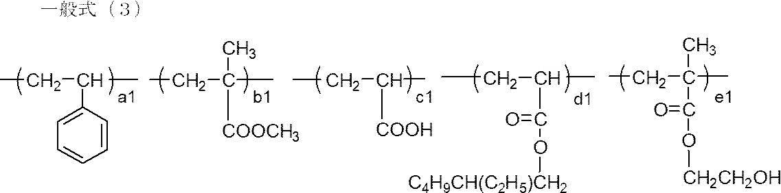
上述の式中、a1、b1、c1、d1、およびe1は各モノマー単位のモル比率を表し、a1は3~60(モル%)、b1は30~95(モル%)、c1は0.5~25(モル%)、d1は0.5~40(モル%)、e1は1~10(モル%)を表す。
a1の好ましい範囲は上述のxの好ましい範囲と同じであり、b1の好ましい範囲は上述のyの好ましい範囲と同じであり、c1の好ましい範囲は上述のzの好ましい範囲と同じであり、d1の好ましい範囲は上述のwの好ましい範囲と同じである。
e1は1~10モル%であり、好ましくは2~9モル%であり、より好ましくは2~8モル%である。
a1の好ましい範囲は上述のxの好ましい範囲と同じであり、b1の好ましい範囲は上述のyの好ましい範囲と同じであり、c1の好ましい範囲は上述のzの好ましい範囲と同じであり、d1の好ましい範囲は上述のwの好ましい範囲と同じである。
e1は1~10モル%であり、好ましくは2~9モル%であり、より好ましくは2~8モル%である。
一般式(1)で表されるポリマーの重量平均分子量は、1000~100万が好ましく、2000~75万がより好ましく、3000~50万が更に好ましい。
一般式(1)で表されるポリマーは、例えば、特許第3305459号および特許第3754745号公報等を参照して合成することができる。
一般式(1)で表されるポリマーは、例えば、特許第3305459号および特許第3754745号公報等を参照して合成することができる。
なお、第1高分子および第2高分子のガラス転移温度としては特に限定されるものではないが、第1高分子のガラス転移温度としては、0℃以上が好ましく、25℃以上がより好ましく、40℃を超えることが更に好ましい。上限としては特に限定されるものではないが、一般に120℃以下が好ましい。
また、第2高分子のガラス転移温度としては特に限定されるものではないが、40℃以下が好ましく、25℃以下がより好ましく、25℃未満が更に好ましく、0℃以下が特に好ましく、0℃未満が最も好ましい。下限としては特に限定されるものではないが、一般に-50℃以上が好ましい。
第1高分子のガラス転移温度と、第2高分子のガラス転移温度の差(絶対値)としては特に限定されるものではないが、一般に20~100℃が好ましい。
また、第2高分子のガラス転移温度としては特に限定されるものではないが、40℃以下が好ましく、25℃以下がより好ましく、25℃未満が更に好ましく、0℃以下が特に好ましく、0℃未満が最も好ましい。下限としては特に限定されるものではないが、一般に-50℃以上が好ましい。
第1高分子のガラス転移温度と、第2高分子のガラス転移温度の差(絶対値)としては特に限定されるものではないが、一般に20~100℃が好ましい。
導電線における金属部は、導電線の導電特性を担保する部分であり、金属部は金属により構成される。金属部を構成する金属としては、導電特性がより優れる点で、金(金属金)、銀(金属銀)、銅(金属銅)、ニッケル(金属ニッケル)、およびパラジウム(金属パラジウム)からなる群より選択される少なくとも1種の金属が好ましい。
なお、図11は導電線50の拡大図である。図11には、金属部54が粒子状になって導電線50に分散した形態を示しているが、金属部54の形態としては粒子状に限定されるものではなく、金属部54が層状(図示せず)となって導電線50に分散した形態であってもよい。
図11に示す導電線50は、第1高分子、および第2高分子を含有するバインダー52と、バインダー52中に分散した複数の金属部54とを含む。金属部54は上述のように粒子状である。
なお、図11は導電線50の拡大図である。図11には、金属部54が粒子状になって導電線50に分散した形態を示しているが、金属部54の形態としては粒子状に限定されるものではなく、金属部54が層状(図示せず)となって導電線50に分散した形態であってもよい。
図11に示す導電線50は、第1高分子、および第2高分子を含有するバインダー52と、バインダー52中に分散した複数の金属部54とを含む。金属部54は上述のように粒子状である。
導電線には上述の以外の材料が含有されていてもよい。上述の以外の材料としては、例えば、非金属の微粒子が挙げられる。非金属の微粒子としては、例えば、樹脂粒子、および、金属酸化物粒子等が挙げられ、金属酸化物粒子が好ましい。
金属酸化物粒子としては、例えば、酸化ケイ素粒子、および、酸化チタン粒子等が挙げられる。
金属酸化物粒子としては、例えば、酸化ケイ素粒子、および、酸化チタン粒子等が挙げられる。
非金属の微粒子の平均粒子径としては特に限定されるものではないが、球相当径で1~1000nmが好ましく、10~500nmがより好ましく、20~200nmが更に好ましい。上述の範囲内であれば、検出部はより優れた透明性を有しやすく、かつ、より優れた導電性を有しやすい。
非金属の微粒子の球相当径は、透過型電子顕微鏡を用いて、任意の50個分の球相当径を算出し、それらを算術平均したものである。
非金属の微粒子の球相当径は、透過型電子顕微鏡を用いて、任意の50個分の球相当径を算出し、それらを算術平均したものである。
<金属安定化剤>
また、導電線は金属部の安定化を目的として、金属安定化剤を金属部表面または内部、あるいはバインダー内に有することが好ましい。金属安定化剤としては以下のような素材を単独または併用して用いることができる。
また、導電線は金属部の安定化を目的として、金属安定化剤を金属部表面または内部、あるいはバインダー内に有することが好ましい。金属安定化剤としては以下のような素材を単独または併用して用いることができる。
特表2009-505358号公報、段落0075~0086記載の腐食防止剤類。
特開2009-188360号公報、段落0077~0092記載の金属イオントラップ剤類。
特開2012-146548号公報、段落0044~0047記載のメルカプト基を有する含窒素複素環化合物類。
特開2013-224397号公報、段落0018~0049記載の銀イオン拡散抑制層形成用組成物類。
特開2014-075115号公報、段落0030~0066銀イオン拡散抑制層形成用の化合物類。
特開2018-024784号公報、段落0050~0057記載の防錆剤類。
特開2019-016488号公報、段落0050~0057記載のメルカプトベンゾチアゾール類。
特開2009-188360号公報、段落0077~0092記載の金属イオントラップ剤類。
特開2012-146548号公報、段落0044~0047記載のメルカプト基を有する含窒素複素環化合物類。
特開2013-224397号公報、段落0018~0049記載の銀イオン拡散抑制層形成用組成物類。
特開2014-075115号公報、段落0030~0066銀イオン拡散抑制層形成用の化合物類。
特開2018-024784号公報、段落0050~0057記載の防錆剤類。
特開2019-016488号公報、段落0050~0057記載のメルカプトベンゾチアゾール類。
また、金属安定化剤として、後述の特定化合物を好ましく使用できる。
金属安定化剤としては以下の化合物またはその塩が好ましい。
2-メルカプトベンゾチアゾール、2-メルカプトベンゾイミダゾール、5-メルカプ-1-フェニル-1Hテトラゾール、1-(4-カルボキシフェニル)-5-メルカプト-1H-テトラゾール、3-メルカプト-1,2,4-トリアゾール、1-(m-スルホフェニル)-5-メルカプト-1H-テトラゾールナトリウム、2-メルカプトベンゾオキサゾール、1,2,3-ベンゾトリアゾール、1-(3-アセトアミドフェニル)-5-メルカプトテトラゾール、5-アミノ-2-メルカプトベンゾイミダゾール、6-アミノ-2-メルカプトベンゾチアゾール、チオシアヌル酸、6-(ジブチルアミノ)-1,3,5-トリアジン-2,4-ジチオール、2-メルカプトチアゾリン、ジエチルジチオカルバミン酸ジエチルアンモニウム、(2-ベンゾチアゾリルチオ)酢酸、3-(2-ベンゾチアゾリルチオ)プロピオン酸、6-(ジブチルアミノ)-1,3,5-トリアジン-2,4-ジチオール、2-アミノ-5-メルカプト-1,3,4-チアジアゾール、2-メルカプト-5-メチルチオ-1,3,4-チアジアゾール、2-メルカプト-5-エチルチオ-1,3,4-チアジアゾール、2-5-ジメルカプト-1,3,4-チアジアゾール、2-チオ酢酸-5メルカプト-1,3,4-チアジアゾール、2-アミノピリミジン、5,6-ジメチルベンゾイミダゾール、2-メルカプトピリミジン。
中でも、金属安定化剤として、メルカプトチアゾール骨格もしくはメルカプトチアジアゾール骨格を有する化合物、またはこれらの塩から選ばれる化合物は、硫化耐性向上に特に有効であり、最も好ましい。最も好ましい化合物の具体例としては、2-メルカプトベンゾチアゾール、5-メチル-2-メルカプトベンゾチアゾール、2-アミノ-5-メルカプト-1,3,4-チアジアゾール、2-メルカプト-5-メチルチオ-1,3,4-チアジアゾール、2-メルカプト-5-エチルチオ-1,3,4-チアジアゾール、2-5-ジメルカプト-1,3,4-チアジアゾールおよびこれらの誘導体または塩が挙げられる。
金属安定化剤としては以下の化合物またはその塩が好ましい。
2-メルカプトベンゾチアゾール、2-メルカプトベンゾイミダゾール、5-メルカプ-1-フェニル-1Hテトラゾール、1-(4-カルボキシフェニル)-5-メルカプト-1H-テトラゾール、3-メルカプト-1,2,4-トリアゾール、1-(m-スルホフェニル)-5-メルカプト-1H-テトラゾールナトリウム、2-メルカプトベンゾオキサゾール、1,2,3-ベンゾトリアゾール、1-(3-アセトアミドフェニル)-5-メルカプトテトラゾール、5-アミノ-2-メルカプトベンゾイミダゾール、6-アミノ-2-メルカプトベンゾチアゾール、チオシアヌル酸、6-(ジブチルアミノ)-1,3,5-トリアジン-2,4-ジチオール、2-メルカプトチアゾリン、ジエチルジチオカルバミン酸ジエチルアンモニウム、(2-ベンゾチアゾリルチオ)酢酸、3-(2-ベンゾチアゾリルチオ)プロピオン酸、6-(ジブチルアミノ)-1,3,5-トリアジン-2,4-ジチオール、2-アミノ-5-メルカプト-1,3,4-チアジアゾール、2-メルカプト-5-メチルチオ-1,3,4-チアジアゾール、2-メルカプト-5-エチルチオ-1,3,4-チアジアゾール、2-5-ジメルカプト-1,3,4-チアジアゾール、2-チオ酢酸-5メルカプト-1,3,4-チアジアゾール、2-アミノピリミジン、5,6-ジメチルベンゾイミダゾール、2-メルカプトピリミジン。
中でも、金属安定化剤として、メルカプトチアゾール骨格もしくはメルカプトチアジアゾール骨格を有する化合物、またはこれらの塩から選ばれる化合物は、硫化耐性向上に特に有効であり、最も好ましい。最も好ましい化合物の具体例としては、2-メルカプトベンゾチアゾール、5-メチル-2-メルカプトベンゾチアゾール、2-アミノ-5-メルカプト-1,3,4-チアジアゾール、2-メルカプト-5-メチルチオ-1,3,4-チアジアゾール、2-メルカプト-5-エチルチオ-1,3,4-チアジアゾール、2-5-ジメルカプト-1,3,4-チアジアゾールおよびこれらの誘導体または塩が挙げられる。
金属安定化剤の導入は、折り曲げ部および非折り曲げ部において金属材料の耐久性向上に有用であり、特に金属部に銀を用いる場合、マイグレーションおよび硫化の抑制に有効であり好ましい。金属安定化剤の導入方法としては、導電線の形成途中または形成後に、金属安定化剤類を含む溶液に導電性フィルムを塗布または浸漬により接触させる方法、またはこれら金属安定化剤類を薫蒸等により気相反応により導電性フィルムに堆積させる方法等を好ましく用いることができる。また、金属安定化剤は、前述の透明絶縁層内に含有させることも好ましい。特に、予め金属安定化剤を透明絶縁層に含有させることにより、金属安定化剤を溶解するために必要な溶媒と導電線との接触の必要がなくなり、溶媒による導電線またはバインダーのダメージを回避でき好ましい。このため、第1の透明絶縁層および第2の透明絶縁層のうち、少なくとも一方が金属安定化剤を含むことが好ましい。
また、タッチパネル10の検出部20の入力領域E1であるアクティブエリアにおける経時による抵抗変化は、折曲部がない構成のタッチパネルにおいても発生する可能性がある。しかしながら、第1の透明絶縁層および第2の透明絶縁層のうち、少なくとも一方が金属安定化剤を含むことにより、上述の折曲部がない構成のタッチパネルにおいても抵抗変化を抑制することができる。
また、タッチパネル10の検出部20の入力領域E1であるアクティブエリアにおける経時による抵抗変化は、折曲部がない構成のタッチパネルにおいても発生する可能性がある。しかしながら、第1の透明絶縁層および第2の透明絶縁層のうち、少なくとも一方が金属安定化剤を含むことにより、上述の折曲部がない構成のタッチパネルにおいても抵抗変化を抑制することができる。
これら金属安定化剤の使用量に制限はないが、透明絶縁層および導電性フィルムのうち、少なくとも一方に、導電層1層あたり、1mg/m2~10g/m2の範囲で含有させることが好ましく、10mg/m2~1g/m2の範囲で含有させることがさらに好ましい。
導電線においても、形状は特に限定されるものではないが、タッチパネルに適用した際により優れたタッチ位置の検出性能が得られるように、線状(直線、曲線、および、これらの組み合わせ等)であるのが好ましい。この際、導電線の線幅は特に限定されるものではないが、導電線の導電特性および視認しづらさのバランスの点から、30μm以下が好ましく、15μm以下がより好ましく、10μm以下が更に好ましく、5μm以下が特に好ましく、4μm以下が最も好ましく、0.5μm以上が好ましく、1.0μm以上がより好ましい。
導電線の厚みは特に限定されるものではないが、薄型化と導電特性のバランスの点で、200μm以下が好ましく、30μm以下がより好ましく、10μm以下が更に好ましく、0.3~5μmであることが特に好ましく、0.5~5μmであることが最も好ましい。
導電線の厚みは特に限定されるものではないが、薄型化と導電特性のバランスの点で、200μm以下が好ましく、30μm以下がより好ましく、10μm以下が更に好ましく、0.3~5μmであることが特に好ましく、0.5~5μmであることが最も好ましい。
<検出部の製造方法>
検出部の製造方法について、導電線の金属部が銀(金属銀)を含有する場合を例にして説明する。より優れた生産性が得られる点で以下工程を有する方法が好ましい。
検出部の製造方法について、導電線の金属部が銀(金属銀)を含有する場合を例にして説明する。より優れた生産性が得られる点で以下工程を有する方法が好ましい。
・工程A:
可撓性基材上に、少なくともハロゲン化銀と第1高分子とを含有するハロゲン化銀含有塗布液と、少なくとも第2高分子を含有する組成調整塗布液とを、同時重層塗布して、ハロゲン化銀感光性層を形成する工程。
・工程B:
ハロゲン化銀感光性層を露光した後、現像処理して金属銀を含有する導電線を形成する工程。
以下では、各工程について詳述する。
可撓性基材上に、少なくともハロゲン化銀と第1高分子とを含有するハロゲン化銀含有塗布液と、少なくとも第2高分子を含有する組成調整塗布液とを、同時重層塗布して、ハロゲン化銀感光性層を形成する工程。
・工程B:
ハロゲン化銀感光性層を露光した後、現像処理して金属銀を含有する導電線を形成する工程。
以下では、各工程について詳述する。
<工程A>
工程Aは、可撓性基材上に、少なくともハロゲン化銀と第1高分子とを含有するハロゲン化銀含有塗布液と、少なくとも第2高分子を含有する組成調整塗布液とを、同時重層塗布して、ハロゲン化銀感光性層を形成する工程である。
なお、同時重層塗布する場合の各塗布液の積層順序としては特に限定されるものではない。可撓性基材側から、ハロゲン化銀含有塗布液、および、組成調整塗布液をこの順に積層してもよい。逆に、可撓性基材側から、組成調整塗布液、および、ハロゲン化銀含有塗布液をこの順に積層してもよい。更に、組成調整塗布液、ハロゲン化銀含有塗布液、および、組成調整塗布液をこの順に積層してもよい。
工程Aは、可撓性基材上に、少なくともハロゲン化銀と第1高分子とを含有するハロゲン化銀含有塗布液と、少なくとも第2高分子を含有する組成調整塗布液とを、同時重層塗布して、ハロゲン化銀感光性層を形成する工程である。
なお、同時重層塗布する場合の各塗布液の積層順序としては特に限定されるものではない。可撓性基材側から、ハロゲン化銀含有塗布液、および、組成調整塗布液をこの順に積層してもよい。逆に、可撓性基材側から、組成調整塗布液、および、ハロゲン化銀含有塗布液をこの順に積層してもよい。更に、組成調整塗布液、ハロゲン化銀含有塗布液、および、組成調整塗布液をこの順に積層してもよい。
なお、「可撓性基材上に塗布」とは、可撓性基材表面上に直接塗布する場合、および、可撓性基材上に別途層が配置され、その層上に塗布する場合も含める。
本工程では、ハロゲン化銀を含むハロゲン化銀含有塗布液と、ハロゲン化銀を含まない組成調整塗布液とを同時重層塗布しているため、両者の塗布液より形成される2層の塗膜の界面にて成分の拡散が進行する。より具体的には、可撓性基材上に配置されるハロゲン化銀含有塗布液から形成される塗膜(以後、塗膜Aともいう)中から、組成調整塗布液から形成される塗膜(以後、塗膜Bともいう)中に一部のハロゲン化銀、および、第1高分子の拡散が進行する。その結果、塗膜B中の塗膜A側の領域にはハロゲン化銀、および、第1高分子が含まれ、その含有量は、塗膜A中のハロゲン化銀、および、第1高分子の含有量よりも少ない。
塗膜B中の塗膜A側の領域(以下「領域w」ともいう。)には、塗膜Aから移動したハロゲン化銀が含有されるため、後述する工程Bを経た後、この領域wは、導電線における上部領域を形成することとなる。このとき、導電線のうち、領域wにおいては第1高分子の含有量および第2高分子の含有量の合計量に対する第2高分子の含有量の含有質量比が、中間領域よりも大きくなりやすい。
本工程では、ハロゲン化銀を含むハロゲン化銀含有塗布液と、ハロゲン化銀を含まない組成調整塗布液とを同時重層塗布しているため、両者の塗布液より形成される2層の塗膜の界面にて成分の拡散が進行する。より具体的には、可撓性基材上に配置されるハロゲン化銀含有塗布液から形成される塗膜(以後、塗膜Aともいう)中から、組成調整塗布液から形成される塗膜(以後、塗膜Bともいう)中に一部のハロゲン化銀、および、第1高分子の拡散が進行する。その結果、塗膜B中の塗膜A側の領域にはハロゲン化銀、および、第1高分子が含まれ、その含有量は、塗膜A中のハロゲン化銀、および、第1高分子の含有量よりも少ない。
塗膜B中の塗膜A側の領域(以下「領域w」ともいう。)には、塗膜Aから移動したハロゲン化銀が含有されるため、後述する工程Bを経た後、この領域wは、導電線における上部領域を形成することとなる。このとき、導電線のうち、領域wにおいては第1高分子の含有量および第2高分子の含有量の合計量に対する第2高分子の含有量の含有質量比が、中間領域よりも大きくなりやすい。
なお、ハロゲン化銀含有塗布液は、少なくともハロゲン化銀と第1高分子とを含有すればよく、第2高分子を更に含有してもよい。この場合、ハロゲン化銀含有塗布液中における第1高分子の含有量および第2高分子の含有量に対する第2高分子の含有質量比は、組成調整塗布液中における第1高分子の含有量および第2高分子の含有量に対する第2高分子の含有質量比よりも小さいことが好ましい。
また、組成調整塗布液は、少なくとも第2高分子を含有すればよく、ハロゲン化銀、および/または、第1高分子を更に含有してもよい。組成調整塗布液が更にハロゲン化銀を含有する場合、その含有量としては特に限定されるものではないが、ハロゲン化銀含有塗布液中におけるハロゲン化銀の含有量より、組成調整塗布液中におけるハロゲン化銀の含有量の方が少ないことが好ましい。そのようにすることで、より外光反射の少ない検出部が得られやすい。
組成調整塗布液が更に第1高分子を含有する場合、組成調整塗布液中における第1高分子の含有量および第2高分子の含有量に対する第1高分子の含有質量比は、ハロゲン化銀含有塗布液における第1高分子の含有量および第2高分子の含有量に対する第1高分子の含有質量比よりも小さいことが好ましい。
組成調整塗布液が更に第1高分子を含有する場合、組成調整塗布液中における第1高分子の含有量および第2高分子の含有量に対する第1高分子の含有質量比は、ハロゲン化銀含有塗布液における第1高分子の含有量および第2高分子の含有量に対する第1高分子の含有質量比よりも小さいことが好ましい。
ハロゲン化銀含有塗布液に含有されるハロゲン化銀としては特に限定されるものではなく、公知のハロゲン化銀が使用できる。ハロゲン化銀に含有されるハロゲン元素は、塩素、臭素、ヨウ素およびフッ素のいずれであってもよく、これらを組み合わせでもよい。例えば、塩化銀、臭化銀、または、ヨウ化銀を主体としたハロゲン化銀が好ましく用いられ、更に臭化銀または塩化銀を主体としたハロゲン化銀が好ましく用いられる。塩臭化銀、沃塩臭化銀、または、沃臭化銀もまた好ましく用いられる。より好ましくは、塩臭化銀、臭化銀、沃塩臭化銀、または、沃臭化銀であり、最も好ましくは、塩化銀50モル%以上を含有する塩臭化銀、または、沃塩臭化銀が用いられる。
なお、ここで、「臭化銀を主体としたハロゲン化銀」とは、ハロゲン化銀組成中に占める臭化物イオンのモル分率が50%以上のハロゲン化銀をいう。この臭化銀を主体としたハロゲン化銀粒子は、臭化物イオンのほかに沃化物イオン、塩化物イオンを含有していてもよい。
なお、ここで、「臭化銀を主体としたハロゲン化銀」とは、ハロゲン化銀組成中に占める臭化物イオンのモル分率が50%以上のハロゲン化銀をいう。この臭化銀を主体としたハロゲン化銀粒子は、臭化物イオンのほかに沃化物イオン、塩化物イオンを含有していてもよい。
ハロゲン化銀は固体粒子状であり、ハロゲン化銀の平均粒子サイズは、球相当径で0.1~1000nm(1μm)であることが好ましく、0.1~300nmであることがより好ましく、1~200nmであることが更に好ましい。
なお、ハロゲン化銀粒子の球相当径とは、粒子形状が球形の同じ体積を有する粒子の直径である。
なお、ハロゲン化銀粒子の球相当径とは、粒子形状が球形の同じ体積を有する粒子の直径である。
ハロゲン化銀粒子の形状は特に限定されず、例えば、球状、立方体状、平板状(6角平板状、三角形平板状、4角形平板状等)、八面体状、および、14面体状等様々な形状であることができる。
また、ハロゲン化銀の安定化または高感化のために用いられるロジウム化合物、イリジウム化合物等のVIII族、VIIB族に属する金属化合物、パラジウム化合物の利用については、特開2009-188360号公報の段落0039~段落0042の記載を参照することができる。更に化学増感については、特開2009-188360号公報の段落0043の技術記載を参照することができる。
また、ハロゲン化銀の安定化または高感化のために用いられるロジウム化合物、イリジウム化合物等のVIII族、VIIB族に属する金属化合物、パラジウム化合物の利用については、特開2009-188360号公報の段落0039~段落0042の記載を参照することができる。更に化学増感については、特開2009-188360号公報の段落0043の技術記載を参照することができる。
ハロゲン化銀含有塗布液に含有され、組成調整塗布液に含有されることがある第1高分子、および、組成調整塗布液に含有され、ハロゲン化銀含有塗布液に含有されることがある第2高分子の形態としては既に説明したとおりであるため、説明は省略する。
ハロゲン化銀含有塗布液、および、組成調整塗布液は、ハロゲン化銀、第1高分子、および、第2高分子以外の成分を含有していてもよく、それらの成分はハロゲン化銀含有塗布液、および、組成調整塗布液において共通であり、以下に説明するとおりである。
ハロゲン化銀含有塗布液、および、組成調整塗布液は、ハロゲン化銀、第1高分子、および、第2高分子以外の成分を含有していてもよく、それらの成分はハロゲン化銀含有塗布液、および、組成調整塗布液において共通であり、以下に説明するとおりである。
ハロゲン化銀含有塗布液、および、組成調整塗布液は、更にゼラチンを含有してもよい。
ゼラチンの種類は特に限定されるものではなく、例えば、石灰処理ゼラチンの他、酸処理ゼラチンを用いてもよく、ゼラチンの加水分解物、ゼラチン酵素分解物、および、アミノ基またはカルボキシル基を修飾したゼラチン(フタル化ゼラチン、アセチル化ゼラチン)を使用することもできる。
ゼラチンの種類は特に限定されるものではなく、例えば、石灰処理ゼラチンの他、酸処理ゼラチンを用いてもよく、ゼラチンの加水分解物、ゼラチン酵素分解物、および、アミノ基またはカルボキシル基を修飾したゼラチン(フタル化ゼラチン、アセチル化ゼラチン)を使用することもできる。
ハロゲン化銀含有塗布液、および、組成調整塗布液は、更に溶媒を含有してもよい。使用される溶媒としては、例えば、水、有機溶媒(例えば、メタノール等のアルコール類、アセトン等のケトン類、ホルムアミド等のアミド類、ジメチルスルホキシド等のスルホキシド類、酢酸エチル等のエステル類、エーテル類等)、イオン性液体、および、これらの混合溶媒を挙げることができる。
ハロゲン化銀含有塗布液、および、組成調整塗布液には、必要に応じて、上述した材料以外の他の材料が含まれていてもよい。例えば、上述の第1高分子および第2高分子を架橋するために使用される架橋剤が含まれることが好ましい。架橋剤が含まれることによりポリマー間での架橋が進行し、後述する工程においてゼラチンが分解除去された際にも金属銀同士の連結が保たれ、結果として導電特性がより優れる。
ハロゲン化銀含有塗布液と組成調整塗布液とを同時重層塗布する方法は特に限定されるものではなく、公知の方法を採用することができ、例えば、ダイ塗布方式を用いることが好ましい。ダイ塗布方式にはスライド塗布方式、エクストルージョン塗布方式、カーテン塗布方式があるが、スライド塗布方式またはエクストルージョン塗布が好ましく、薄層塗布適性が高いエクストルージョン塗布が最も好ましい。
なお、上述の同時重層塗布する際には、上述したタッチパネル用導電性フィルムの第1実施態様の形態が得られやすい点から、所定の基板上に塗布した際に形成される膜(表面膜)の乾燥厚みが300nm以上となるような組成の第2高分子を含有する組成調整塗布液を使用することが好ましい。
また、同時重層塗布を実施した後、得られた塗膜に対して、必要に応じて、乾燥処理を施してもよい。乾燥処理を実施することにより、ハロゲン化銀含有塗布液より得られる塗膜および組成調整塗布液より得られる塗膜に含まれる溶媒を容易に除去することができる。
上述の処理により、ハロゲン化銀を含有する感光性層を可撓性基材上に形成することができる。なお、本明細書では、上述の「ハロゲン化銀を含有する感光性層」を「ハロゲン化銀感光性層」、または、単に「感光性層」ということがある。
<工程B>
工程Bは、ハロゲン化銀感光性層を露光した後、現像処理して金属銀を含有する導電線を形成する工程である。
本工程により、ハロゲン化銀が還元され、金属銀を含む導電線が形成される。なお、通常、露光処理はパターン状に実施され、露光部では金属銀を含む導電線が形成される。一方、非露光部では、後述する現像処理によってハロゲン化銀が溶出される。上述のゼラチンおよび上述の高分子を含む非導電線が形成される。非導電線には実質的に金属銀が含まれておらず、非導電線とは導電性を示さない領域を意図する。
以下では、本工程で実施される露光処理と現像処理とについて詳述する。
工程Bは、ハロゲン化銀感光性層を露光した後、現像処理して金属銀を含有する導電線を形成する工程である。
本工程により、ハロゲン化銀が還元され、金属銀を含む導電線が形成される。なお、通常、露光処理はパターン状に実施され、露光部では金属銀を含む導電線が形成される。一方、非露光部では、後述する現像処理によってハロゲン化銀が溶出される。上述のゼラチンおよび上述の高分子を含む非導電線が形成される。非導電線には実質的に金属銀が含まれておらず、非導電線とは導電性を示さない領域を意図する。
以下では、本工程で実施される露光処理と現像処理とについて詳述する。
露光処理は、感光性層に露光を行う処理である。感光性層に対してパターン状の露光を施すことにより、露光領域における感光性層中のハロゲン化銀が潜像を形成する。この潜像が形成された領域は、後述する現像処理によって導電線を形成する。一方、露光がなされなかった未露光領域では、後述する現像処理の際にハロゲン化銀が溶解して感光性層から流出し、透明な膜(非導電線)が得られる。
露光の際に使用される光源は特に限定されるものではなく、可視光線、紫外線等の光、または、X線等の放射線等が挙げられる。
パターン露光を行う方法は特に限定されるものではなく、例えば、フォトマスクを利用した面露光で行ってもよいし、レーザービームによる走査露光で行ってもよい。なお、パターンの形状は特に限定されるものではなく、形成したい導電線のパターンに合わせて適宜調整される。
露光の際に使用される光源は特に限定されるものではなく、可視光線、紫外線等の光、または、X線等の放射線等が挙げられる。
パターン露光を行う方法は特に限定されるものではなく、例えば、フォトマスクを利用した面露光で行ってもよいし、レーザービームによる走査露光で行ってもよい。なお、パターンの形状は特に限定されるものではなく、形成したい導電線のパターンに合わせて適宜調整される。
現像処理の方法は特に限定されるものではないが、例えば、銀塩写真フイルム、印画紙、印刷製版用フイルム、および、フォトマスク用エマルジョンマスク等に用いられる通常の現像処理の技術を用いることができる。
現像処理の際に使用される現像液の種類は特に限定されるものではないが、例えば、PQ(phenidone hydroquinone)現像液、MQ(Metol hydroquinone)現像液、および、MAA(メトール・アスコルビン酸)現像液等を用いることもできる。
現像処理は、未露光部分の銀塩を除去して安定化させる目的で行われる定着処理を含むことができる。定着処理は、銀塩写真フイルム、印画紙、印刷製版用フイルム、および、フォトマスク用エマルジョンマスク等に用いられる定着処理の技術を用いることができる。
定着工程における定着温度は、約20℃~約50℃が好ましく、25~45℃がより好ましい。また、定着時間は5秒~1分が好ましく、7秒~50秒がより好ましい。
現像、定着処理を施した感光性層は、水洗処理および安定化処理を施されるのが好ましい。
現像処理の際に使用される現像液の種類は特に限定されるものではないが、例えば、PQ(phenidone hydroquinone)現像液、MQ(Metol hydroquinone)現像液、および、MAA(メトール・アスコルビン酸)現像液等を用いることもできる。
現像処理は、未露光部分の銀塩を除去して安定化させる目的で行われる定着処理を含むことができる。定着処理は、銀塩写真フイルム、印画紙、印刷製版用フイルム、および、フォトマスク用エマルジョンマスク等に用いられる定着処理の技術を用いることができる。
定着工程における定着温度は、約20℃~約50℃が好ましく、25~45℃がより好ましい。また、定着時間は5秒~1分が好ましく、7秒~50秒がより好ましい。
現像、定着処理を施した感光性層は、水洗処理および安定化処理を施されるのが好ましい。
上述の工程Aおよび工程B以外のその他の工程を有していてもよい。
その他の工程としては、例えば、
工程Bの後に、導電線の金属銀同士を互いに融着させる工程F;
工程Aの後であって、工程Bの前に、ハロゲン化銀感光性層と、金属吸着性置換基または金属吸着性構造を有する化合物(以下、「特定化合物」ともいう。)と、を接触させる工程C1;
工程Bの後であって、工程Fの前に、導電線と特定化合物とを接触させる工程C2;
工程Bの後であって、工程Fの前に、更に、導電線を圧密化する工程D;
ハロゲン化銀含有塗布液、および、組成調整塗布液からなる群より選択される少なくとも1種が、ゼラチンを含有する場合に、工程Bの後であって、工程Dの前に、導電線中のゼラチンを除去する工程E;等が挙げられる。また、その他の工程としては、後述する易接着層形成工程等も挙げられる。以下では、その他の工程について説明する。
その他の工程としては、例えば、
工程Bの後に、導電線の金属銀同士を互いに融着させる工程F;
工程Aの後であって、工程Bの前に、ハロゲン化銀感光性層と、金属吸着性置換基または金属吸着性構造を有する化合物(以下、「特定化合物」ともいう。)と、を接触させる工程C1;
工程Bの後であって、工程Fの前に、導電線と特定化合物とを接触させる工程C2;
工程Bの後であって、工程Fの前に、更に、導電線を圧密化する工程D;
ハロゲン化銀含有塗布液、および、組成調整塗布液からなる群より選択される少なくとも1種が、ゼラチンを含有する場合に、工程Bの後であって、工程Dの前に、導電線中のゼラチンを除去する工程E;等が挙げられる。また、その他の工程としては、後述する易接着層形成工程等も挙げられる。以下では、その他の工程について説明する。
(工程F)
工程Fは、工程Bの後に、導電線の(導電線に含有される)金属銀同士を互いに融着させる工程である。本工程により、金属銀同士が融着する結果、より優れた導電性を有する導電線を備えた検出部が得られる。
工程Fは、工程Bの後に、導電線の(導電線に含有される)金属銀同士を互いに融着させる工程である。本工程により、金属銀同士が融着する結果、より優れた導電性を有する導電線を備えた検出部が得られる。
加熱の方法としては特に限定されるものではないが、導電線を有する可撓性基材を過熱蒸気に接触させる処理が挙げられる。
過熱蒸気としては特に限定されるものではなく、過熱水蒸気でよいし、過熱水蒸気に他のガスを混合させたものでもよい。
過熱蒸気は、供給時間10~300秒の範囲で導電線に接触させることが好ましい。供給時間が10秒以上であると、導電率の向上が大きい。また、300秒以下だと、十分に導電率が向上するため、経済性の点からより好ましい。
また、過熱蒸気は、供給量が500~600g/m3の範囲で導電線に接触させることが好ましく、過熱蒸気の温度は、1気圧で100~160℃に制御されることが好ましい。
過熱蒸気としては特に限定されるものではなく、過熱水蒸気でよいし、過熱水蒸気に他のガスを混合させたものでもよい。
過熱蒸気は、供給時間10~300秒の範囲で導電線に接触させることが好ましい。供給時間が10秒以上であると、導電率の向上が大きい。また、300秒以下だと、十分に導電率が向上するため、経済性の点からより好ましい。
また、過熱蒸気は、供給量が500~600g/m3の範囲で導電線に接触させることが好ましく、過熱蒸気の温度は、1気圧で100~160℃に制御されることが好ましい。
加熱処理の他の方法としては、80~150℃での加熱処理が挙げられる。
加熱時間は特に限定されるものではないが、上述の効果がより優れる点で、0.1~5.0時間が好ましく、0.5~1.0時間がより好ましい。
加熱時間は特に限定されるものではないが、上述の効果がより優れる点で、0.1~5.0時間が好ましく、0.5~1.0時間がより好ましい。
(工程C1)
工程C1は、工程Aの後であって、工程Bの前に実施され、ハロゲン化銀感光性層と、特定化合物とを接触させる工程である。本工程によって、後段の工程Bにおいて生じた金属銀同士がより融着しにくくなる。本工程においては、ハロゲン化銀感光性層に特定化合物を接触させるため、ハロゲン化銀感光性層のより表面に近い領域(界面領域)において、金属銀同士が融着しにくくなるという効果を有する。従って、特に後段の工程によって得られる導電線において、界面領域において金属銀同士の融着がより阻害されやすい。また、この場合であっても、導電線の中間領域においては、十分に金属銀同士が融着するものと考えられ、優れた導電性を有する検出部が得られる。
工程C1は、工程Aの後であって、工程Bの前に実施され、ハロゲン化銀感光性層と、特定化合物とを接触させる工程である。本工程によって、後段の工程Bにおいて生じた金属銀同士がより融着しにくくなる。本工程においては、ハロゲン化銀感光性層に特定化合物を接触させるため、ハロゲン化銀感光性層のより表面に近い領域(界面領域)において、金属銀同士が融着しにくくなるという効果を有する。従って、特に後段の工程によって得られる導電線において、界面領域において金属銀同士の融着がより阻害されやすい。また、この場合であっても、導電線の中間領域においては、十分に金属銀同士が融着するものと考えられ、優れた導電性を有する検出部が得られる。
検出部の製造方法は、工程C1または後述する工程C2を有することが好ましく、工程C1および工程C2を有していてもよい。
特定化合物とハロゲン化銀感光性層を接触させる方法としては特に限定されるものではないが、典型的には特定化合物が溶解、および/または、分散された溶液と、ハロゲン化銀感光性層とを接触させる方法が挙げられる。また、特定化合物を含有する気体と、ハロゲン化銀感光性層とを接触させる方法であってもよい。
特定化合物を含有する溶液とハロゲン化銀感光性層とを接触させる方法としては特に限定されるものではないが、溶液にハロゲン化銀感光性層を浸漬させる方法、および、ハロゲン化銀感光性層に溶液を塗布する方法等が挙げられ、溶液にハロゲン化銀感光性層を浸漬させる方法がより好ましい。溶液にハロゲン化銀感光性層を浸漬させる方法は、より簡便な装置で、より安定的に実施でき、また、浸漬後に洗浄すれば、余剰の溶液をより容易に除去できるため、好ましい。
また、ハロゲン化銀感光性層と、金属吸着性部位を有する化合物を含有する気体、および/または、溶液とを接触させる方法は、ハロゲン化銀感光性層の表面において、金属銀が上述の化合物に吸着されやすいという特徴も有する。これにより、導電線の表面において金属銀が互いに融着するのがより阻害されやすい。
特定化合物は、金属吸着性置換基または金属吸着性構造(以下、これらをあわせて「金属吸着性部位」ともいう。)を有する化合物である。
金属吸着性置換基としては、特に限定されるものではないが、金属吸着性置換基としては、カルボキシル基またはその塩、酸アミド基、アミノ基、イミダゾール基、ピラゾール基、チオール基、チオエーテル基、および、ジスルフィド基からなる群より選択される少なくとも1種が好ましい。
金属吸着性構造としては特に限定されるものではないが、含窒素ヘテロ環が好ましく、5または6員環アゾール類が好ましく、5員環アゾール類がより好ましい。
含窒素ヘテロ環としては、例えば、テトラゾール環、トリアゾール環、イミダゾール環、チアジアゾール環、オキサジアゾール環、セレナジアゾール環、オキサゾール環、チアゾール環、ベンズオキサゾール環、ベンズチアゾール環、ベンズイミダゾール環、ピリミジン環、トリアザインデン環、テトラアザインデン環、ベンゾインダゾール環、ベンゾトリアゾール環、ベンゾオキサゾール環、ベンゾチアゾール環、ピリジン環、キノリン環、ピペリジン環、ピペラジン環、キノキサリン環、モルホリン環、および、ペンタアザインデン環等が挙げられる。
これらの環は、置換基を有してもよく、置換基としては、ニトロ基、ハロゲン原子(例えば、塩素原子、および、臭素原子)、シアノ基、置換もしくは無置換のアルキル基(例えば、メチル基、エチル基、プロピル基、t-ブチル基、および、シアノエチル基の各基)、アリール基(例えば、フェニル基、4-メタンスルホンアミドフェニル基、4-メチルフェニル基、3,4-ジクロルフェニル基、および、ナフチル基の各基)、アルケニル基(例えば、アリル基)、アラルキル基(例えば、ベンジル基、4-メチルベンジル基、および、フェネチル基の各基)、スルホニル基(例えば、メタンスルホニル基、エタンスルホニル基、および、p-トルエンスルホニル基の各基)、カルバモイル基(例えば、無置換カルバモイル基、メチルカルバモイル基、および、フェニルカルバモイル基の各基)、スルファモイル基(例えば、無置換スルファモイル基、メチルスルファモイル基、および、フェニルスルファモイル基の各基)、カルボンアミド基(例えば、アセトアミド基、および、ベンズアミド基の各基)、スルホンアミド基(例えば、メタンスルホンアミド基、ベンゼンスルホンアミド基、および、p-トルエンスルホンアミド基の各基)、アシルオキシ基(例えば、アセチルオキシ基、および、ベンゾイルオキシ基の各基)、スルホニルオキシ基(例えば、メタンスルホニルオキシ基)、ウレイド基(例えば、無置換ウレイド基、メチルウレイド基、エチルウレイド基、および、フェニルウレイド基の各基)、アシル基(例えば、アセチル基、および、ベンゾイル基の各基)、オキシカルボニル基(例えば、メトキシカルボニル基、および、フェノキシカルボニル基の各基)、および、ヒドロキシル基等が挙げられる。置換基は、1つの環に複数置換してもよい。
含窒素ヘテロ環としては、例えば、テトラゾール環、トリアゾール環、イミダゾール環、チアジアゾール環、オキサジアゾール環、セレナジアゾール環、オキサゾール環、チアゾール環、ベンズオキサゾール環、ベンズチアゾール環、ベンズイミダゾール環、ピリミジン環、トリアザインデン環、テトラアザインデン環、ベンゾインダゾール環、ベンゾトリアゾール環、ベンゾオキサゾール環、ベンゾチアゾール環、ピリジン環、キノリン環、ピペリジン環、ピペラジン環、キノキサリン環、モルホリン環、および、ペンタアザインデン環等が挙げられる。
これらの環は、置換基を有してもよく、置換基としては、ニトロ基、ハロゲン原子(例えば、塩素原子、および、臭素原子)、シアノ基、置換もしくは無置換のアルキル基(例えば、メチル基、エチル基、プロピル基、t-ブチル基、および、シアノエチル基の各基)、アリール基(例えば、フェニル基、4-メタンスルホンアミドフェニル基、4-メチルフェニル基、3,4-ジクロルフェニル基、および、ナフチル基の各基)、アルケニル基(例えば、アリル基)、アラルキル基(例えば、ベンジル基、4-メチルベンジル基、および、フェネチル基の各基)、スルホニル基(例えば、メタンスルホニル基、エタンスルホニル基、および、p-トルエンスルホニル基の各基)、カルバモイル基(例えば、無置換カルバモイル基、メチルカルバモイル基、および、フェニルカルバモイル基の各基)、スルファモイル基(例えば、無置換スルファモイル基、メチルスルファモイル基、および、フェニルスルファモイル基の各基)、カルボンアミド基(例えば、アセトアミド基、および、ベンズアミド基の各基)、スルホンアミド基(例えば、メタンスルホンアミド基、ベンゼンスルホンアミド基、および、p-トルエンスルホンアミド基の各基)、アシルオキシ基(例えば、アセチルオキシ基、および、ベンゾイルオキシ基の各基)、スルホニルオキシ基(例えば、メタンスルホニルオキシ基)、ウレイド基(例えば、無置換ウレイド基、メチルウレイド基、エチルウレイド基、および、フェニルウレイド基の各基)、アシル基(例えば、アセチル基、および、ベンゾイル基の各基)、オキシカルボニル基(例えば、メトキシカルボニル基、および、フェノキシカルボニル基の各基)、および、ヒドロキシル基等が挙げられる。置換基は、1つの環に複数置換してもよい。
上述の化合物としては含窒素6員環を有する化合物(含窒素6員環化合物)が好ましく、含窒素6員環化合物としては、トリアジン環、ピリミジン環、ピリジン環、ピロリン環、ピペリジン環、ピリダジン環、または、ピラジン環を有する化合物が好ましく、トリアジン環またはピリミジン環を有する化合物がより好ましい。これらの含窒素6員環化合物は置換基を有していてもよく、置換基としては、炭素数1~6(好ましくは1~3)のアルキル基、炭素数1~6(好ましくは1~3)のアルコキシ基、水酸基、カルボキシル基、メルカプト基、炭素数1~6(好ましくは1~3)のアルコキシアルキル基、および、炭素数1~6(好ましくは1~3)のヒドロキシアルキル基が挙げられる。
含窒素6員環化合物の具体例としては、トリアジン、メチルトリアジン、ジメチルトリアジン、ヒドロキシエチルトリアジン、ピリミジン、4-メチルピリミジン、ピリジン、および、ピロリンが挙げられる。
含窒素6員環化合物の具体例としては、トリアジン、メチルトリアジン、ジメチルトリアジン、ヒドロキシエチルトリアジン、ピリミジン、4-メチルピリミジン、ピリジン、および、ピロリンが挙げられる。
上述の化合物は、金属吸着性部位の1種を単独で有しても、2種以上を有してもよいが、上述の化合物は、2種以上の金属吸着性部位を有していることが好ましい。
(工程C2)
工程C2は、工程Bの後であって、工程Fの前に実施され、導電線と、特定化合物とを接触させる工程である。本工程によって、導電線の(導電線に含まれる)金属銀同士がより融着しにくくなる。本工程においては、導電線に特定化合物を接触させるため、導電線のより表面に近い領域(界面領域)において、金属銀同士が融着しにくくなるという効果を有する。従って、導電線の界面領域において金属銀同士の融着がより阻害されやすい。また、この場合であっても、導電線の中間領域においては、十分に金属銀同士が融着するものと考えられ、優れた導電性を有する検出部が得られる。
工程C2は、工程Bの後であって、工程Fの前に実施され、導電線と、特定化合物とを接触させる工程である。本工程によって、導電線の(導電線に含まれる)金属銀同士がより融着しにくくなる。本工程においては、導電線に特定化合物を接触させるため、導電線のより表面に近い領域(界面領域)において、金属銀同士が融着しにくくなるという効果を有する。従って、導電線の界面領域において金属銀同士の融着がより阻害されやすい。また、この場合であっても、導電線の中間領域においては、十分に金属銀同士が融着するものと考えられ、優れた導電性を有する検出部が得られる。
なお、本工程において、導電線と特定化合物とを接触させる方法、および、特定化合物の形態等については、既に説明した工程C1における各形態と同様であるため、説明を省略する。
(工程D)
工程Dは、工程Bの後であって上述の工程Fの前に、導電線を圧密化する工程である。本工程によって、導電線の導電性がより向上するとともに、導電線の可撓性基材への密着性がより向上しやすい。
工程Dは、工程Bの後であって上述の工程Fの前に、導電線を圧密化する工程である。本工程によって、導電線の導電性がより向上するとともに、導電線の可撓性基材への密着性がより向上しやすい。
導電線を圧密化する方法としては特に限定されるものではないが、例えば、導電線を有する可撓性基材を、少なくとも一対のロール間を加圧下で通過させるカレンダ処理工程が好ましい。以下、カレンダーロールを用いた圧密化処理をカレンダ処理と記す。
カレンダ処理に用いられるロールとしては、プラスチックロールおよび金属ロールが挙げられる。シワ防止の点からプラスチックロールが好ましい。ロール間の圧力としては特に限定されるものではない。ロール間の圧力は、富士フイルム株式会社製プレスケール(高圧用)を用いて測定できる。
カレンダ処理に用いられるロールの表面粗さRaは、得られる導電線がより視認されにくい点で、0~2.0μmが好ましく、0.3~1.0μmがより好ましい。
カレンダ処理に用いられるロールの表面粗さRaは、得られる導電線がより視認されにくい点で、0~2.0μmが好ましく、0.3~1.0μmがより好ましい。
圧密化処理の温度は特に限定されるものではないが、10℃(温調なし)~100℃が好ましく、導電線のパターンの画線密度、形状、および、バインダー種によって異なるが、10℃(温調なし)~50℃がより好ましい。
(工程E)
ハロゲン化銀含有塗布液、および、組成調整塗布液からなる群より選択される少なくとも1種が、ゼラチンを含有する場合に、工程Eは、工程Bの後であって、工程Dの前に、導電線(導電線に含有される)のゼラチンを除去する工程である。ゼラチンを除去することにより、結果として導電線の金属銀の含有量が相対的に高まるため、より優れた導電性を有する導電線が得られる。
工程Eはゼラチンの全部を除去する工程であってもよいし、ゼラチンの一部を除去する工程であってもよい。また、工程Eにおいては、導電線に加えて、可撓性基材上の導電線以外の部分(例えば、非導電線)からゼラチンを除去してもよい。
ハロゲン化銀含有塗布液、および、組成調整塗布液からなる群より選択される少なくとも1種が、ゼラチンを含有する場合に、工程Eは、工程Bの後であって、工程Dの前に、導電線(導電線に含有される)のゼラチンを除去する工程である。ゼラチンを除去することにより、結果として導電線の金属銀の含有量が相対的に高まるため、より優れた導電性を有する導電線が得られる。
工程Eはゼラチンの全部を除去する工程であってもよいし、ゼラチンの一部を除去する工程であってもよい。また、工程Eにおいては、導電線に加えて、可撓性基材上の導電線以外の部分(例えば、非導電線)からゼラチンを除去してもよい。
ゼラチンを除去する方法としては特に限定されるものではないが、例えば、タンパク質分解酵素を用いて分解除去する方法、および、所定の酸化剤を用いて分解除去する方法が挙げられる。
なお、タンパク質分解酵素を用いてゼラチンを分解除去する方法としては、例えば、特開2014-209332号公報の段落0084~0077に記載の方法を採用できる。
また、酸化剤を用いてゼラチンを分解除去する方法としては、例えば、特開2014-112512号公報の段落0064~0066に記載の方法を採用できる。
なお、タンパク質分解酵素を用いてゼラチンを分解除去する方法としては、例えば、特開2014-209332号公報の段落0084~0077に記載の方法を採用できる。
また、酸化剤を用いてゼラチンを分解除去する方法としては、例えば、特開2014-112512号公報の段落0064~0066に記載の方法を採用できる。
(易接着層形成工程)
易接着層形成工程は、工程Aの前に、可撓性基材上に易接着層(以下、「下塗り層」ともいう。)を形成し、易接着層(下塗り層)付き可撓性基材を得る工程である。可撓性基材上に下塗り層を形成する方法としては特に限定されるものではないが、可撓性基材上に下塗り層形成用組成物を塗布する方法が挙げられる。下塗り層形成工程では、形成される下塗り層が、隣接する他の層(可撓性基材、および、非導電線等)との間で、屈折率の差の絶対値がより小さくなるよう、調整されることが好ましい。下塗り層と隣接する他の層との間の屈折率の差を調整する方法としては特に限定されるものではないが、各層の形成に用いられる組成物中に含有される各成分の種類を調整する方法が挙げられる。
易接着層形成工程は、工程Aの前に、可撓性基材上に易接着層(以下、「下塗り層」ともいう。)を形成し、易接着層(下塗り層)付き可撓性基材を得る工程である。可撓性基材上に下塗り層を形成する方法としては特に限定されるものではないが、可撓性基材上に下塗り層形成用組成物を塗布する方法が挙げられる。下塗り層形成工程では、形成される下塗り層が、隣接する他の層(可撓性基材、および、非導電線等)との間で、屈折率の差の絶対値がより小さくなるよう、調整されることが好ましい。下塗り層と隣接する他の層との間の屈折率の差を調整する方法としては特に限定されるものではないが、各層の形成に用いられる組成物中に含有される各成分の種類を調整する方法が挙げられる。
易接着層を形成する方法としては特に限定されるものではないが、易接着層形成用組成物を可撓性基材上に塗布して、必要に応じて加熱処理を施す方法が挙げられる。易接着層形成用組成物は、溶媒を含有してもよい。溶媒の種類は特に限定されるものではなく、ハロゲン化銀含有塗布液等が含有することがある溶媒として既に説明したとおりである。
易接着層の厚みは特に限定されるものではないが、可撓性基材と、ハロゲン化銀感光性層および導電線との密着性がより向上する点で、0.02~0.3μmが好ましい。
易接着層としては特に限定されるものではなく、例えば、特開2008-208310号公報に記載の第1接着層の好適な適用例を、好適に用いることができる。
易接着層の厚みは特に限定されるものではないが、可撓性基材と、ハロゲン化銀感光性層および導電線との密着性がより向上する点で、0.02~0.3μmが好ましい。
易接着層としては特に限定されるものではなく、例えば、特開2008-208310号公報に記載の第1接着層の好適な適用例を、好適に用いることができる。
<検出部の他の製造方法>
検出部、取出し配線部を構成する金属細線の製造方法は、上述の方法に、特に限定されるものではなく、例えば、めっき法、蒸着法および印刷法等が適宜利用可能である。
検出部、取出し配線部を構成する金属細線の製造方法は、上述の方法に、特に限定されるものではなく、例えば、めっき法、蒸着法および印刷法等が適宜利用可能である。
めっき法よる金属細線の形成方法について説明する。例えば、金属細線は、無電解めっき下地層に無電解めっきすることにより下地層上に形成される金属めっき膜で構成することができる。この場合、少なくとも金属微粒子を含有する触媒インクを基材上にパターン状に形成した後に、基材を無電解めっき浴に浸漬し、金属めっき膜を形成することで形成される。より具体的には、特開2014-159620号公報に記載の金属被膜基材の製造方法を利用することができる。また、少なくとも金属触媒前駆体と相互作用しうる官能基を有する樹脂組成物を基材上にパターン状に形成した後、触媒または触媒前駆体を付与し、基材を無電解めっき浴に浸漬し、金属めっき膜を形成することで形成される。より具体的には、特開2012-144761号公報に記載の金属被膜基材の製造方法を応用することができる。
また、蒸着法よる金属細線の形成方法について説明する。まず、蒸着により、銅箔層を形成し、フォトリソグラフィー法により銅箔層から銅配線を形成することにより、金属細線を形成することができる。銅箔層は、蒸着銅箔以外にも、電解銅箔が利用可能である。より具体的には、特開2014-29614号公報に記載の銅配線を形成する工程を利用することができる。
また、印刷法よる金属細線の形成方法について説明する。まず、導電性粉末を含有する導電性ペーストを金属細線と同じパターンで基板に塗布し、その後、加熱処理を施すことにより金属細線を形成することができる。導電性ペーストを用いたパターン形成は、例えば、インクジェット法またはスクリーン印刷法でなされる。導電性ペーストとしては、より具体的には、特開2011-28985号公報に記載の導電性ペーストを利用することができる。
また、印刷法よる金属細線の形成方法について説明する。まず、導電性粉末を含有する導電性ペーストを金属細線と同じパターンで基板に塗布し、その後、加熱処理を施すことにより金属細線を形成することができる。導電性ペーストを用いたパターン形成は、例えば、インクジェット法またはスクリーン印刷法でなされる。導電性ペーストとしては、より具体的には、特開2011-28985号公報に記載の導電性ペーストを利用することができる。
<封止層>
封止層は、導電性フィルムの導電層の硫化を抑制するためのものである。封止層は、電気を絶縁する材料であれば、特に限定されるものではない。例えば、封止層は、電気的な絶縁性を有する粘着層で構成される。粘着層としては、例えば、粘着テープを用いることができる。
また、封止層は、ガスクロマトグラフィー法を用いた硫黄ガス(硫化水素ガス)のガス透過性が10-2g/m2/day以下である材料により構成することが好ましい。ガス透過性の下限値は、0g/m2/dayである。本発明では、ガスクロマトグラフィー法にGC-FPD(Gas Chromatograph-Flame Photometric Detector)法を用いる。
封止層は、ポリイミドテープ、またはシリコーン、Al2O3、SiONもしくはウレタン樹脂で構成されることが好ましい。
また、封止層の厚みは30nm以上200μm以下であることが好ましい。封止層の厚みが30nm以下では、上述の硫化の抑制の効果が得られにくい。一方、封止層の厚みが200μmを超えると封止層が厚くなりすぎ、封止層の形成に多くの時間がかかったり、貼り付ける場合には折曲部への追従性が悪かったり、封止層が脆い材質の場合には割れが生じるおそれがある。
封止層の形成方法は、折曲部全面に封止層を形成することができる方法であれば、特に限定されるものではなく、貼り付け法、スパッタ法、蒸着法、スプレー塗布法、塗布法、およびディスペンサー法等を利用することができる。貼り付け法は、ポリイミドテープ等の電気絶縁性を有するテープを貼り付けることにより、封止層を形成する方法である。
封止層は、導電性フィルムの導電層の硫化を抑制するためのものである。封止層は、電気を絶縁する材料であれば、特に限定されるものではない。例えば、封止層は、電気的な絶縁性を有する粘着層で構成される。粘着層としては、例えば、粘着テープを用いることができる。
また、封止層は、ガスクロマトグラフィー法を用いた硫黄ガス(硫化水素ガス)のガス透過性が10-2g/m2/day以下である材料により構成することが好ましい。ガス透過性の下限値は、0g/m2/dayである。本発明では、ガスクロマトグラフィー法にGC-FPD(Gas Chromatograph-Flame Photometric Detector)法を用いる。
封止層は、ポリイミドテープ、またはシリコーン、Al2O3、SiONもしくはウレタン樹脂で構成されることが好ましい。
また、封止層の厚みは30nm以上200μm以下であることが好ましい。封止層の厚みが30nm以下では、上述の硫化の抑制の効果が得られにくい。一方、封止層の厚みが200μmを超えると封止層が厚くなりすぎ、封止層の形成に多くの時間がかかったり、貼り付ける場合には折曲部への追従性が悪かったり、封止層が脆い材質の場合には割れが生じるおそれがある。
封止層の形成方法は、折曲部全面に封止層を形成することができる方法であれば、特に限定されるものではなく、貼り付け法、スパッタ法、蒸着法、スプレー塗布法、塗布法、およびディスペンサー法等を利用することができる。貼り付け法は、ポリイミドテープ等の電気絶縁性を有するテープを貼り付けることにより、封止層を形成する方法である。
<第1の透明絶縁層および第2の透明絶縁層>
第1の透明絶縁層および第2の透明絶縁層は、上述の光学的に透明な粘着剤(OCA、Optical Clear Adhesive)およびUV(Ultra Violet)硬化樹脂等の光学的に透明な樹脂(OCR、Optical Clear Resin)に限定されるものではない。
第1の透明絶縁層および第2の透明絶縁層は、可撓性基材の表面および裏面において、検出部および取出し配線部がない領域、および検出部上および取出し配線部上にこれらを覆うように配置してもよい。この場合、第1の透明絶縁層および第2の透明絶縁層は、透明であり、かつ電気絶縁性を有するものであり、さらに検出部および取出し配線部を保護する機能を有する。第1の透明絶縁層および第2の透明絶縁層は、導通性が十分に低い。第1の透明絶縁層および第2の透明絶縁層により検出部および取出し配線部は、金属細線間の導電性、および他の部材と導電性が十分に低い状態とされ、金属細線同士の導通、および他の部材との導通が抑制され短絡等が防止される。
第1の透明絶縁層および第2の透明絶縁層を、検出部および取出し配線部の一部が露出するように、すなわち、検出部および取出し配線部の一部を覆わないように配置してもよい。第1の透明絶縁層および第2の透明絶縁層は、上述のように光学的に透明な粘着剤および光学的に透明な樹脂を用いることができるが、これに限定されるものではなく、以下に示すものを用いることができる。以下、第1の透明絶縁層および第2の透明絶縁層をまとめて、単に透明絶縁層という。
なお、1回の塗布工程によって透明絶縁層を形成できる点から、入力領域E1および外側領域E2の両方の同一の透明絶縁層が配置されることが好ましい。
第1の透明絶縁層および第2の透明絶縁層は、上述の光学的に透明な粘着剤(OCA、Optical Clear Adhesive)およびUV(Ultra Violet)硬化樹脂等の光学的に透明な樹脂(OCR、Optical Clear Resin)に限定されるものではない。
第1の透明絶縁層および第2の透明絶縁層は、可撓性基材の表面および裏面において、検出部および取出し配線部がない領域、および検出部上および取出し配線部上にこれらを覆うように配置してもよい。この場合、第1の透明絶縁層および第2の透明絶縁層は、透明であり、かつ電気絶縁性を有するものであり、さらに検出部および取出し配線部を保護する機能を有する。第1の透明絶縁層および第2の透明絶縁層は、導通性が十分に低い。第1の透明絶縁層および第2の透明絶縁層により検出部および取出し配線部は、金属細線間の導電性、および他の部材と導電性が十分に低い状態とされ、金属細線同士の導通、および他の部材との導通が抑制され短絡等が防止される。
第1の透明絶縁層および第2の透明絶縁層を、検出部および取出し配線部の一部が露出するように、すなわち、検出部および取出し配線部の一部を覆わないように配置してもよい。第1の透明絶縁層および第2の透明絶縁層は、上述のように光学的に透明な粘着剤および光学的に透明な樹脂を用いることができるが、これに限定されるものではなく、以下に示すものを用いることができる。以下、第1の透明絶縁層および第2の透明絶縁層をまとめて、単に透明絶縁層という。
なお、1回の塗布工程によって透明絶縁層を形成できる点から、入力領域E1および外側領域E2の両方の同一の透明絶縁層が配置されることが好ましい。
透明絶縁層としては、架橋構造が導入され、かつ透明絶縁層の押し込み硬度が所定の範囲に調整されたものを用いることができる。
金属細線のひび割れおよび断線は、保存環境条件を含めた導電性フィルムの折り曲げ形態に伴う応力により発生していると推測される。このため、金属細線の表面に、その応力を緩和すること、および、金属細線の強度を補強する機能を有した透明絶縁層を敷設することにより、金属細線のひび割れ、および断線が防止できる。具体的には、強度を補強する機能を透明絶縁層に付与するために、透明絶縁層に架橋構造が導入され、透明絶縁層の優位な剛性が維持される。また、折り曲げに伴い透明絶縁層にクラックが生じて金属細線が断線することに繋がらないように、透明絶縁層の押し込み硬度が所定の範囲内に調整されている。
金属細線のひび割れおよび断線は、保存環境条件を含めた導電性フィルムの折り曲げ形態に伴う応力により発生していると推測される。このため、金属細線の表面に、その応力を緩和すること、および、金属細線の強度を補強する機能を有した透明絶縁層を敷設することにより、金属細線のひび割れ、および断線が防止できる。具体的には、強度を補強する機能を透明絶縁層に付与するために、透明絶縁層に架橋構造が導入され、透明絶縁層の優位な剛性が維持される。また、折り曲げに伴い透明絶縁層にクラックが生じて金属細線が断線することに繋がらないように、透明絶縁層の押し込み硬度が所定の範囲内に調整されている。
透明絶縁層の押し込み硬度は、200MPa以下であり、150MPa以下が好ましく、130MPa以下がより好ましい。下限は特に制限されないが、10MPa以上が好ましい。押し込み硬度が200MPa以下の場合、所望の効果を得やすい。
透明絶縁層の押し込み硬度は、微小硬度試験機(ピコデンタ―)により測定することができる。
なお、透明絶縁層が上述の押し込み硬度を示すために、透明絶縁層を構成する樹脂の主鎖構造が柔らかい構造であること、または、架橋点間の距離が長い構造であることが好ましい。
透明絶縁層の押し込み硬度は、微小硬度試験機(ピコデンタ―)により測定することができる。
なお、透明絶縁層が上述の押し込み硬度を示すために、透明絶縁層を構成する樹脂の主鎖構造が柔らかい構造であること、または、架橋点間の距離が長い構造であることが好ましい。
透明絶縁層は、50~90℃における弾性率が1×10⁵Pa以上であることが好ましく、1×10⁶~1×10¹⁰MPaであることがより好ましい。可撓性基材が熱膨張すると、可撓性基材上に形成された可撓性基材よりも膨張率の低い金属細線も同様に延び、これにより金属細線の断線が生じることがある。それに対して、透明絶縁層の50~90℃における弾性率が上述の範囲内であれば、高温高湿環境下にて導電性フィルムを折り曲げた状態で使用しても、透明絶縁層が硬く延びにくいため、金属細線のひび割れおよび断線が生じにくい。
また、透明絶縁層の温度85℃および相対湿度85%での弾性率は、1×10⁵Pa以上であることが好ましく、1×10⁶Pa以上であることがより好ましく、1.5×10⁶Pa以上であることがさらに好ましい。上限は特に制限されないが、1×10¹⁰MPa以下の場合が多い。弾性率が上述の範囲内であれば、高温高湿環境下にて導電性フィルムを折り曲げた状態で使用しても、金属細線のひび割れおよび断線がより生じにくい。
なお、透明絶縁層の上述の弾性率は、所定の測定環境、例えば、温度85℃および相対湿度85%にて、微小硬度試験機(ピコデンター)により測定することができる。
また、透明絶縁層の温度85℃および相対湿度85%での弾性率は、1×10⁵Pa以上であることが好ましく、1×10⁶Pa以上であることがより好ましく、1.5×10⁶Pa以上であることがさらに好ましい。上限は特に制限されないが、1×10¹⁰MPa以下の場合が多い。弾性率が上述の範囲内であれば、高温高湿環境下にて導電性フィルムを折り曲げた状態で使用しても、金属細線のひび割れおよび断線がより生じにくい。
なお、透明絶縁層の上述の弾性率は、所定の測定環境、例えば、温度85℃および相対湿度85%にて、微小硬度試験機(ピコデンター)により測定することができる。
透明絶縁層の線膨張率は特に制限されないが、1~500ppm/℃が好ましく、5~200ppm/℃がより好ましく、5~150ppm/℃がさらに好ましい。透明絶縁層の線膨張率が上述の範囲内であれば、高温高湿環境下にて導電性フィルムを折り曲げた状態で使用しても金属細線のひび割れおよび断線がより生じにくい。
なお、透明絶縁層の線膨張率は、透明絶縁層からなる測定試料に熱を加えた際のカール値(カールの曲率半径)を測定し、以下の2つの式より算出することができる。
式1:(透明絶縁層の線膨張率-可撓性基材の線膨張率)×温度差=測定試料の歪み
式2:測定試料の歪み={(可撓性基材の弾性率×(可撓性基材の厚み)2}/{3×(1-可撓性基材のポアソン比)×透明絶縁層の弾性率×カールの曲率半径}
なお、金属細線の断線をより抑制できる点で、透明絶縁層の線膨張率は、可撓性基材の線膨張率との差が小さいことが好ましく、上限は、差分が300ppm/℃以下であることが好ましく、150ppm/℃以下であることがより好ましい。下限は特に制限されないが、0ppm/℃が挙げられる。
なお、透明絶縁層の線膨張率は、透明絶縁層からなる測定試料に熱を加えた際のカール値(カールの曲率半径)を測定し、以下の2つの式より算出することができる。
式1:(透明絶縁層の線膨張率-可撓性基材の線膨張率)×温度差=測定試料の歪み
式2:測定試料の歪み={(可撓性基材の弾性率×(可撓性基材の厚み)2}/{3×(1-可撓性基材のポアソン比)×透明絶縁層の弾性率×カールの曲率半径}
なお、金属細線の断線をより抑制できる点で、透明絶縁層の線膨張率は、可撓性基材の線膨張率との差が小さいことが好ましく、上限は、差分が300ppm/℃以下であることが好ましく、150ppm/℃以下であることがより好ましい。下限は特に制限されないが、0ppm/℃が挙げられる。
透明絶縁層の厚みは特に制限されないが、厚みが大きいと折り曲げた際に透明絶縁層にクラックが生じやすくなる。クラックを抑制しつつ、検出部および取出し配線部の密着性がより優れ、膜強度がより優れる観点から、1~20μmが好ましく、5~15μmがより好ましい。
透明絶縁層は、上述のように光を透過させる性質を有する。
なお、透明絶縁層を含む導電性フィルムの全光線透過率は、可視光領域(波長400~700nm)に対し、85%以上であることが好ましく、90%以上であることがより好ましい。
なお、上述の全光線透過率は、分光測色計CM-3600A(コニカミノルタ株式会社製)によって測定される。
なお、透明絶縁層自体の全光線透過率は、導電性フィルムが上述の全光線透過率を示すように調整されることが好ましく、少なくとも85%以上であることが好ましい。
なお、透明絶縁層を含む導電性フィルムの全光線透過率は、可視光領域(波長400~700nm)に対し、85%以上であることが好ましく、90%以上であることがより好ましい。
なお、上述の全光線透過率は、分光測色計CM-3600A(コニカミノルタ株式会社製)によって測定される。
なお、透明絶縁層自体の全光線透過率は、導電性フィルムが上述の全光線透過率を示すように調整されることが好ましく、少なくとも85%以上であることが好ましい。
透明絶縁層は、検出部および取出し配線部との密着性に優れることが好ましく、具体的には、3M社製「610」よるテープ密着力評価試験で剥離がないことがより好ましい。
また、透明絶縁層は、検出部および取出し配線部だけでなく、可撓性基材(または、下塗り層もしくはバインダー層)の検出部および取出し配線部の形成されていない領域とも接するため、可撓性基材(または、下塗り層もしくはバインダー層)との密着性に優れていることが好ましい。なお、バインダー層とは、可撓性基材上であって金属細線間に配置されるバインダーからなる層であり、ハロゲン化銀法により金属細線を製造する際に形成される場合が多い。
上述のように透明絶縁層と可撓性基材および検出部および取出し配線部との密着性が高い場合、金属細線のひび割れおよび断線をより抑制することができる。
また、透明絶縁層は、検出部および取出し配線部だけでなく、可撓性基材(または、下塗り層もしくはバインダー層)の検出部および取出し配線部の形成されていない領域とも接するため、可撓性基材(または、下塗り層もしくはバインダー層)との密着性に優れていることが好ましい。なお、バインダー層とは、可撓性基材上であって金属細線間に配置されるバインダーからなる層であり、ハロゲン化銀法により金属細線を製造する際に形成される場合が多い。
上述のように透明絶縁層と可撓性基材および検出部および取出し配線部との密着性が高い場合、金属細線のひび割れおよび断線をより抑制することができる。
導電性フィルムの表面反射を抑制する観点から、透明絶縁層の屈折率と、可撓性基材の屈折率との屈折率差が小さいほど好ましい。
また、検出部および取出し配線部の金属細線にバインダー成分が含まれている場合には、透明絶縁層の屈折率と、上述のバインダー成分の屈折率との屈折率差が小さいほど好ましく、透明絶縁層を形成する樹脂成分と、上述のバインダー成分とが同じ材料であることがより好ましい。
なお、透明絶縁層を形成する樹脂成分と、上述のバインダー成分とが同じ材料であるとは、バインダー成分および透明絶縁層を形成する樹脂成分のいずれもが(メタ)アクリル系樹脂である場合が一例として挙げられる。
また、検出部および取出し配線部の金属細線にバインダー成分が含まれている場合には、透明絶縁層の屈折率と、上述のバインダー成分の屈折率との屈折率差が小さいほど好ましく、透明絶縁層を形成する樹脂成分と、上述のバインダー成分とが同じ材料であることがより好ましい。
なお、透明絶縁層を形成する樹脂成分と、上述のバインダー成分とが同じ材料であるとは、バインダー成分および透明絶縁層を形成する樹脂成分のいずれもが(メタ)アクリル系樹脂である場合が一例として挙げられる。
さらに、上述のとおり導電性フィルムを用いてタッチパネルに構成する場合、導電性フィルムの透明絶縁層に、さらに光学的に透明な粘着シートまたは粘着層を貼り合せることがある。透明絶縁層と、光学的に透明な粘着シートまたは粘着層との界面での光散乱を抑制するため、透明絶縁層の屈折率と、光学的に透明な粘着シートの屈折率または粘着層の屈折率との屈折率差は小さいほど好ましい。
透明絶縁層は、架橋構造を含む。架橋構造が含まれることにより、高温高湿環境下にて導電性フィルムを折り曲げた状態で使用しても金属細線の断線が生じにくい。
架橋構造を形成するためには、後述するように、多官能化合物を用いて透明絶縁層を形成することが好ましい。
架橋構造を形成するためには、後述するように、多官能化合物を用いて透明絶縁層を形成することが好ましい。
透明絶縁層を構成する材料は、上述した特性を示す層が得られれば特に制限されない。
なかでも、透明絶縁層の特性の制御が容易である点から、重合性基を有する重合性化合物を含む透明絶縁層形成用組成物を用いて形成される層であることが好ましい。
以下では、透明絶縁層形成用組成物を用いた態様について詳述する。
なかでも、透明絶縁層の特性の制御が容易である点から、重合性基を有する重合性化合物を含む透明絶縁層形成用組成物を用いて形成される層であることが好ましい。
以下では、透明絶縁層形成用組成物を用いた態様について詳述する。
(透明絶縁層の形成方法)
透明絶縁層形成用組成物を用いて透明絶縁層を形成する方法は特に制限されない。例えば、可撓性基材および検出部および取出し配線部上に透明絶縁層形成用組成物を塗布して、必要に応じて塗膜に硬化処理を施し、透明絶縁層を形成する方法(塗布法)、または、仮基板上に透明絶縁層を形成して、検出部および取出し配線部表面に転写する方法(転写法)等が挙げられる。なかでも、厚みの制御がしやすい観点からは、塗布法が好ましい。
透明絶縁層形成用組成物を用いて透明絶縁層を形成する方法は特に制限されない。例えば、可撓性基材および検出部および取出し配線部上に透明絶縁層形成用組成物を塗布して、必要に応じて塗膜に硬化処理を施し、透明絶縁層を形成する方法(塗布法)、または、仮基板上に透明絶縁層を形成して、検出部および取出し配線部表面に転写する方法(転写法)等が挙げられる。なかでも、厚みの制御がしやすい観点からは、塗布法が好ましい。
塗布法の場合に、透明絶縁層形成用組成物を可撓性基材および検出部および取出し配線部上に塗布する方法は特に制限されず、公知の方法(例えば、グラビアコーター、コンマコーター、バーコーター、ナイフコーター、ダイコーターもしくはロールコーター等の塗布法式、インクジェット方式、または、スクリーン印刷方式等)を使用できる。
取り扱い性および製造効率の観点からは、透明絶縁層形成用組成物を可撓性基材および検出部および取出し配線部上に塗布し、必要に応じて乾燥処理を行って残存する溶剤を除去して、塗膜を形成する態様が好ましい。
なお、乾燥処理の条件は特に制限されないが、生産性がより優れる点で、室温~220℃(好ましくは50~120℃)で、1~30分間(好ましく1~10分間)実施することが好ましい。
生産性の観点からは、さらに、透明絶縁層形成用組成物は溶剤成分を含まず、乾燥工程がない状況が好ましい。
なお、乾燥処理の条件は特に制限されないが、生産性がより優れる点で、室温~220℃(好ましくは50~120℃)で、1~30分間(好ましく1~10分間)実施することが好ましい。
生産性の観点からは、さらに、透明絶縁層形成用組成物は溶剤成分を含まず、乾燥工程がない状況が好ましい。
なお、塗布法の場合、硬化処理としては、光硬化処理および熱硬化処理のいずれであってもよい。なかでも、可撓性基材へのダメージを軽減し、タクトタイムを短くする観点で、光硬化処理が好ましい。
露光する方法は特に制限されないが、例えば、活性光線または放射線を照射する方法が挙げられる。活性光線による照射としては、UV(紫外線)ランプ、および、可視光線等による光照射等が用いられる。光源としては、例えば、水銀灯、メタルハライドランプ、キセノンランプ、ケミカルランプ、および、カーボンアーク灯等が挙げられる。また、放射線としては、電子線、X線、イオンビーム、および、遠赤外線等が挙げられる。
塗膜を露光することにより、塗膜中の化合物に含まれる重合性基が活性化され、化合物間の架橋が生じ、層の硬化が進行する。露光エネルギーは10~8000mJ/cm2程度であればよく、好ましくは50~3000mJ/cm2の範囲である。
露光する方法は特に制限されないが、例えば、活性光線または放射線を照射する方法が挙げられる。活性光線による照射としては、UV(紫外線)ランプ、および、可視光線等による光照射等が用いられる。光源としては、例えば、水銀灯、メタルハライドランプ、キセノンランプ、ケミカルランプ、および、カーボンアーク灯等が挙げられる。また、放射線としては、電子線、X線、イオンビーム、および、遠赤外線等が挙げられる。
塗膜を露光することにより、塗膜中の化合物に含まれる重合性基が活性化され、化合物間の架橋が生じ、層の硬化が進行する。露光エネルギーは10~8000mJ/cm2程度であればよく、好ましくは50~3000mJ/cm2の範囲である。
透明絶縁層形成用組成物には、重合性基を有する重合性化合物が含まれる。重合性化合物中に含まれる重合性基の数は特に制限されず、1つであっても、複数であってもよい。なかでも、透明絶縁層中に架橋構造を形成し得る点で、2以上の重合性基を有する重合性化合物を用いることが好ましい。
重合性基の種類は特に制限されず、例えば、(メタ)アクリロイル基、ビニル基、アリル基等のラジカル重合性基、および、エポキシ基、オキセタン基等のカチオン重合性基等が挙げられる。なかでも、反応性の点で、ラジカル重合性基が好ましく、(メタ)アクリロイル基がより好ましい。
重合性化合物は、モノマー、オリゴマーおよびポリマーから選ばれるいずれの形態であってもよい。つまり、重合性化合物は、重合性基を有するオリゴマーであっても、重合性基を有するポリマーであってもよい。
なお、モノマーとしては分子量が1,000未満である化合物が好ましい。
また、オリゴマーおよびポリマーは、有限個(一般的には5~100個)のモノマーが結合した重合体である。オリゴマーとは重量平均分子量が3000以下である化合物であり、ポリマーとは重量平均分子量が3000超である化合物である。
重合性化合物は、1種であっても、複数種を併用してもよい。
重合性基の種類は特に制限されず、例えば、(メタ)アクリロイル基、ビニル基、アリル基等のラジカル重合性基、および、エポキシ基、オキセタン基等のカチオン重合性基等が挙げられる。なかでも、反応性の点で、ラジカル重合性基が好ましく、(メタ)アクリロイル基がより好ましい。
重合性化合物は、モノマー、オリゴマーおよびポリマーから選ばれるいずれの形態であってもよい。つまり、重合性化合物は、重合性基を有するオリゴマーであっても、重合性基を有するポリマーであってもよい。
なお、モノマーとしては分子量が1,000未満である化合物が好ましい。
また、オリゴマーおよびポリマーは、有限個(一般的には5~100個)のモノマーが結合した重合体である。オリゴマーとは重量平均分子量が3000以下である化合物であり、ポリマーとは重量平均分子量が3000超である化合物である。
重合性化合物は、1種であっても、複数種を併用してもよい。
透明絶縁層形成用組成物の好適態様としては、2以上の重合性基を有する重合性化合物(多官能化合物)、並びに、ウレタン(メタ)アクリレート化合物およびエポキシ(メタ)アクリレート化合物の少なくとも一方を含む態様が挙げられる。
なお、2以上の重合性基を有するウレタン(メタ)アクリレート化合物は、上述のウレタン(メタ)アクリレート化合物に該当し、多官能化合物には含まれない。また、2以上の重合性基を有するエポキシ(メタ)アクリレート化合物は、上述のエポキシ(メタ)アクリレート化合物に該当し、多官能化合物には含まれない。
なお、2以上の重合性基を有するウレタン(メタ)アクリレート化合物は、上述のウレタン(メタ)アクリレート化合物に該当し、多官能化合物には含まれない。また、2以上の重合性基を有するエポキシ(メタ)アクリレート化合物は、上述のエポキシ(メタ)アクリレート化合物に該当し、多官能化合物には含まれない。
多官能化合物としては、2以上の重合性基を有していればよく、2以上の(メタ)アクリロイル基を有する化合物が好ましい。
具体的には、2官能の(メタ)アクリレートとしては、例えば、エチレングリコールジ(メタ)アクリレート、ジエチレングリコールジ(メタ)アクリレート、トリエチレングリコールジ(メタ)アクリレート、テトラエチレングリコールジ(メタ)アクリレート、1,4-ブタンジオールジ(メタ)アクリレート、1,6-ヘキサンジオールジ(メタ)アクリレート、1,9-ノナンジオールジ(メタ)アクリレート、グリセリンジ(メタ)アクリレート、ネオペンチルグリコールジ(メタ)アクリレート、3-メチル-1,5ペンタンジオールジ(メタ)アクリレート、2-ブチル-2-エチル-1,3プロパンジ(メタ)アクリレート、ジメチロールトリシクロデカンジ(メタ)アクリレート、プロピレングリコールジ(メタ)アクリレート、ジプロピレングリコールジ(メタ)アクリレート、トリプロピレングリコールジ(メタ)アクリレート、テトラプロピレングリコールジ(メタ)アクリレート、ネオペンチルグリコールヒドロキシピバレートジ(メタ)アクリレート、1,3ブタンジオールジ(メタ)アクリレート、ジメチロールジシクロペンタンジアクリレート、ヘキサメチレングリコールジアクリレート、ヘキサエチレングリコールジ(メタ)アクリレート、ポリエチレングリコールジ(メタ)アクリレート、ポリプロピレングリコールジ(メタ)アクリレート、ブチレングリコールジ(メタ)アクリレート、2,2’-ビス(4-アクリロキシジエトキシフェニル)プロパン、および、ビスフェノールAテトラエチレングリコールジアクリレート等が挙げられる。
具体的には、2官能の(メタ)アクリレートとしては、例えば、エチレングリコールジ(メタ)アクリレート、ジエチレングリコールジ(メタ)アクリレート、トリエチレングリコールジ(メタ)アクリレート、テトラエチレングリコールジ(メタ)アクリレート、1,4-ブタンジオールジ(メタ)アクリレート、1,6-ヘキサンジオールジ(メタ)アクリレート、1,9-ノナンジオールジ(メタ)アクリレート、グリセリンジ(メタ)アクリレート、ネオペンチルグリコールジ(メタ)アクリレート、3-メチル-1,5ペンタンジオールジ(メタ)アクリレート、2-ブチル-2-エチル-1,3プロパンジ(メタ)アクリレート、ジメチロールトリシクロデカンジ(メタ)アクリレート、プロピレングリコールジ(メタ)アクリレート、ジプロピレングリコールジ(メタ)アクリレート、トリプロピレングリコールジ(メタ)アクリレート、テトラプロピレングリコールジ(メタ)アクリレート、ネオペンチルグリコールヒドロキシピバレートジ(メタ)アクリレート、1,3ブタンジオールジ(メタ)アクリレート、ジメチロールジシクロペンタンジアクリレート、ヘキサメチレングリコールジアクリレート、ヘキサエチレングリコールジ(メタ)アクリレート、ポリエチレングリコールジ(メタ)アクリレート、ポリプロピレングリコールジ(メタ)アクリレート、ブチレングリコールジ(メタ)アクリレート、2,2’-ビス(4-アクリロキシジエトキシフェニル)プロパン、および、ビスフェノールAテトラエチレングリコールジアクリレート等が挙げられる。
3官能の(メタ)アクリレートとしては、例えば、トリメチロールプロパントリ(メタ)アクリレート、エチレンオキサイド変性トリメチロールプロパントリ(メタ)アクリレート、プロピレンオキサイド変性トリメチロールプロパントリ(メタ)アクリレート、トリス(アクリロキシエチル)イソシアヌレート、カプロラクトン変性トリス(アクリロキシエチル)イソシアヌレート、ペンタエリスリトールトリ(メタ)アクリレート、ジペンタエリスリトールトリ(メタ)アクリレート、アルキル変性ジペンタエリスリトールトリ(メタ)アクリレート、テトラメチロールメタントリ(メタ)アクリレート、エチレンオキシド変性グリセロールトリアクリレート、プロピレンオキシド変性グリセロールトリアクリレート、εカプロラクトン変性トリメチロールプロパントリアクリレート、および、ペンタエリスリトールトリアクリレート等が挙げられる。
4官能の(メタ)アクリレートとしては、例えば、ジトリメチロールプロパンテトラ(メタ)アクリレート、ペンタエリスリトールエトキシテトラ(メタ)アクリレート、および、ペンタエリスリトールテトラ(メタ)アクリレートが挙げられる。
5官能以上の(メタ)アクリレート化合物としては、例えば、ジペンタエリスリトールペンタ(メタ)アクリレート、アルキル変性ジペンタエリスリトールペンタ(メタ)アクリレート、ジペンタエリスリトールヘキサ(メタ)アクリレート、カプロラクトン変性ジペンタエリスリトールヘキサ(メタ)アクリレート、および、ポリペンタエリスリトールポリアクリレート等が挙げられる。
透明絶縁層形成用組成物中における多官能化合物の含有量は特に制限されないが、本発明の効果がより優れる点で、透明絶縁層形成用組成物中の全固形分に対して、0~50質量%が好ましく、20~45質量%がより好ましい。
ウレタン(メタ)アクリレート化合物は、詳しくは、アクリロイルオキシ基、アクリロイル基、メタクリロイルオキシ基、および、メタクリロイル基からなる群から選ばれる光重合性基を1分子中に2つ以上含み、かつ、ウレタン結合を1分子中に1つ以上含む化合物であることが好ましい。このような化合物は、例えば、イソシアネートとヒドロキシ基含有(メタ)アクリレート化合物とのウレタン化反応によって製造することができる。なお、ウレタン(メタ)アクリレート化合物としては、いわゆるオリゴマーであっても、ポリマーであってもよい。
上述の光重合性基は、ラジカル重合可能な重合性基である。光重合性基を1分子中に2つ以上含む多官能のウレタン(メタ)アクリレート化合物は、高硬度な透明絶縁層を形成するうえで有用である。
ウレタン(メタ)アクリレート化合物1分子中に含まれる光重合性基の数は、少なくとも2つであることが好ましく、例えば、2~10つがより好ましく、2~6つがさらに好ましい。なお、ウレタン(メタ)アクリレート化合物に含まれる2つ以上の光重合性基は同一のものであっても、異なるものであってもよい。
光重合性基としては、アクリロイルオキシ基またはメタクリロイルオキシ基が好ましい。
上述の光重合性基は、ラジカル重合可能な重合性基である。光重合性基を1分子中に2つ以上含む多官能のウレタン(メタ)アクリレート化合物は、高硬度な透明絶縁層を形成するうえで有用である。
ウレタン(メタ)アクリレート化合物1分子中に含まれる光重合性基の数は、少なくとも2つであることが好ましく、例えば、2~10つがより好ましく、2~6つがさらに好ましい。なお、ウレタン(メタ)アクリレート化合物に含まれる2つ以上の光重合性基は同一のものであっても、異なるものであってもよい。
光重合性基としては、アクリロイルオキシ基またはメタクリロイルオキシ基が好ましい。
ウレタン(メタ)アクリレート化合物1分子中に含まれるウレタン結合の数は、1つ以上であればよく、形成される透明絶縁層の硬度がより高くなる点で、2つ以上が好ましく、例えば、2~5つがより好ましい。
なお、1分子中にウレタン結合を2つ含むウレタン(メタ)アクリレート化合物において、光重合性基は一方のウレタン結合のみに直接または連結基を介して結合していてもよく、2つのウレタン結合にそれぞれ直接または連結基を介して結合していてもよい。
一態様では、連結基を介して結合している2つのウレタン結合に、それぞれ1つ以上の光重合性基が結合していることが、好ましい。
なお、1分子中にウレタン結合を2つ含むウレタン(メタ)アクリレート化合物において、光重合性基は一方のウレタン結合のみに直接または連結基を介して結合していてもよく、2つのウレタン結合にそれぞれ直接または連結基を介して結合していてもよい。
一態様では、連結基を介して結合している2つのウレタン結合に、それぞれ1つ以上の光重合性基が結合していることが、好ましい。
上述のように、ウレタン(メタ)アクリレート化合物中において、ウレタン結合と光重合性基は直接結合していてもよく、ウレタン結合と光重合性基との間に連結基が存在していてもよい。連結基は特に限定されるものではなく、直鎖または分岐の飽和または不飽和の炭化水素基、環状基、およびこれらの2つ以上の組み合わせからなる基、等を挙げることができる。上述の炭化水素基の炭素数は、例えば、2~20程度であるが、特に限定されるものではない。また、環状基に含まれる環状構造としては、一例として、脂肪族環(シクロヘキサン環等)、芳香族環(ベンゼン環、ナフタレン環等)等が挙げられる。上述の基は、無置換であっても置換基を有していてもよい。
なお、本明細書において、特記しない限り、記載されている基は置換基を有してもよく無置換であってもよい。ある基が置換基を有する場合、置換基としては、アルキル基(例えば、炭素数1~6のアルキル基)、ヒドロキシ基、アルコキシル基(例えば、炭素数1~6のアルコキシル基)、ハロゲン原子(例えば、フッ素原子、塩素原子、臭素原子)、シアノ基、アミノ基、ニトロ基、アシル基、および、カルボキシル基等を挙げることができる。
なお、本明細書において、特記しない限り、記載されている基は置換基を有してもよく無置換であってもよい。ある基が置換基を有する場合、置換基としては、アルキル基(例えば、炭素数1~6のアルキル基)、ヒドロキシ基、アルコキシル基(例えば、炭素数1~6のアルコキシル基)、ハロゲン原子(例えば、フッ素原子、塩素原子、臭素原子)、シアノ基、アミノ基、ニトロ基、アシル基、および、カルボキシル基等を挙げることができる。
上述のウレタン(メタ)アクリレート化合物は、公知の方法で合成することができる。また、市販品として入手することも可能である。
合成方法の一例としては、例えば、アルコール、ポリオール、および/またはヒドロキシル基含有(メタ)アクリレート等のヒドロキシ基含有化合物とイソシアネートとを反応させる方法が挙げられる。また、必要に応じて、上述の反応によって得られたウレタン化合物を(メタ)アクリル酸でエステル化する方法を挙げることができる。なお、(メタ)アクリル酸とは、アクリル酸とメタクリル酸を包含する意味で用いるものとする。
合成方法の一例としては、例えば、アルコール、ポリオール、および/またはヒドロキシル基含有(メタ)アクリレート等のヒドロキシ基含有化合物とイソシアネートとを反応させる方法が挙げられる。また、必要に応じて、上述の反応によって得られたウレタン化合物を(メタ)アクリル酸でエステル化する方法を挙げることができる。なお、(メタ)アクリル酸とは、アクリル酸とメタクリル酸を包含する意味で用いるものとする。
上述のイソシアネートとしては、例えば、芳香族系、脂肪族系、および、脂環式系等のポリイソシアネートが挙げられ、トリレンジイソシアネート、ジフェニルメタンジイソシアネート、水添化ジフェニルメタンジイソシアネート、ポリフェニルメタンポリイソシアネート、変性ジフェニルメタンジイソシアネート、水添化キシリレンジイソシアネート、キシリレンジイソシアネート、ヘキサメチレンジイソシアネート、トリメチルヘキサメチレンジイソシアネート、テトラメチルキシリレンジイソシアネート、イソホロンジイソシアネート、ノルボルネンジイソシアネート、1,3-ビス(イソシアナトメチル)シクロヘキサン、フェニレンジイソシアネート、リジンジイソシアネート、リジントリイソシアネート、および、ナフタレンジイソシアネート等が挙げられる。これらは1種でもよく2種以上を併用してもよい。
上述のヒドロキシ基含有(メタ)アクリレートとしては、例えば、2-ヒドロキシエチルアクリレート、2-ヒドロキシプロピルアクリレート、2-ヒドロキシブチルアクリレート、4-ヒドロキシブチルアクリレート、2-ヒドロキシエチルアクリロイルホスフェート、2-アクリロイロキシエチル-2-ヒドロキシプロピルフタレート、グリセリンジアクリレート、2-ヒドロキシ-3-アクリロイロキシプロピルアクリレート、ペンタエリスリトールトリアクリレート、ジペンタエリスリトールペンタアクリレート、カプロラクトン変性2-ヒドロキシエチルアクリレート、および、シクロヘキサンジメタノールモノアクリレート等が挙げられる。これらは1種でもよく2種以上を併用してもよい。
ウレタン(メタ)アクリレート化合物の市販品としては、下記のものに限定されるものではないが、例えば、共栄社化学社製UA-306H、UA-306I、UA-306T、UA-510H、UF-8001G、UA-101I、UA-101T、AT-600、AH-600、AI-600、新中村化学社製U-4HA、U-6HA、U-6LPA、UA-32P、U-15HA、UA-1100H、日本合成化学工業社製紫光UV-1400B、同UV-1700B、同UV-6300B、同UV-7550B、同UV-7600B、同UV-7605B、同UV-7610B、同UV-7620EA、同UV-7630B、同UV-7640B、同UV-6630B、同UV-7000B、同UV-7510B、同UV-7461TE、同UV-3000B、同UV-3200B、同UV-3210EA、同UV-3310EA、同UV-3310B、同UV-3500BA、同UV-3520TL、同UV-3700B、同UV-6100B、同UV-6640B、同UV-2000B、同UV-2010B、同UV-2250EAを挙げることができる。また、日本合成化学工業社製紫光UV-2750B、共栄社化学社製UL-503LN、大日本インキ化学工業社製ユニディック17-806、同17-813、同V-4030、同V-4000BA、ダイセルUCB社製EB-1290K、トクシキ製ハイコープAU-2010、同AU-2020等も挙げられる。
6官能以上のウレタン(メタ)アクリレート化合物としては、例えば、根上工業(株)製のアートレジンUN-3320HA、アートレジンUN-3320HC、アートレジンUN-3320HS、アートレジンUN-904、日本合成化学(株)製の紫光UV-1700B、紫光UV-7605B、紫光UV-7610B、紫光UV-7630B、紫光UV-7640B、新中村化学工業(株)製のNKオリゴU-6PA、NKオリゴU-10HA、NKオリゴU-10PA、NKオリゴU-1100H、NKオリゴU-15HA、NKオリゴU-53H、NKオリゴU-33H、ダイセル・サイテック(株)製のKRM8452、EBECRYL1290、KRM8200、EBECRYL5129、KRM8904、日本化薬(株)製のUX-5000等を挙げることができる。
また、2~3官能のウレタン(メタ)アクリレート化合物としては、Nagase(株)製のナトコUV自己治癒、DIC株式会社製のEXP DX‐40等も挙げることができる。
6官能以上のウレタン(メタ)アクリレート化合物としては、例えば、根上工業(株)製のアートレジンUN-3320HA、アートレジンUN-3320HC、アートレジンUN-3320HS、アートレジンUN-904、日本合成化学(株)製の紫光UV-1700B、紫光UV-7605B、紫光UV-7610B、紫光UV-7630B、紫光UV-7640B、新中村化学工業(株)製のNKオリゴU-6PA、NKオリゴU-10HA、NKオリゴU-10PA、NKオリゴU-1100H、NKオリゴU-15HA、NKオリゴU-53H、NKオリゴU-33H、ダイセル・サイテック(株)製のKRM8452、EBECRYL1290、KRM8200、EBECRYL5129、KRM8904、日本化薬(株)製のUX-5000等を挙げることができる。
また、2~3官能のウレタン(メタ)アクリレート化合物としては、Nagase(株)製のナトコUV自己治癒、DIC株式会社製のEXP DX‐40等も挙げることができる。
上述のウレタン(メタ)アクリレート化合物の分子量(重量平均分子量Mw)は、300~10,000の範囲が好ましい。分子量がこの範囲であれば、柔軟性に優れ、且つ、表面硬度に優れた透明絶縁層を得ることができる。
また、エポキシ(メタ)アクリレート化合物としては、ポリグリシジルエーテルと(メタ)アクリル酸との付加反応により得られるものをいい、分子内に(メタ)アクリロイル基を少なくとも2個有している場合が多い。
透明絶縁層形成用組成物中におけるウレタン(メタ)アクリレート化合物およびエポキシ(メタ)アクリレート化合物の合計含有量は特に制限されないが、本発明の効果がより優れる点で、透明絶縁層形成用組成物中の全固形分に対して、10~70質量%が好ましく、30~65質量%がより好ましい。
透明絶縁層形成用組成物には、さらに、単官能モノマーが含まれていてもよく、単官能(メタ)アクリレートが含まれていることが好ましい。単官能モノマーは、透明絶縁層中での架橋密度を制御するための希釈モノマーとして機能する。
単官能(メタ)アクリレートとしては、例えば、ブチル(メタ)アクリレート、アミル(メタ)アクリレート、2-エチルヘキシル(メタ)アクリレート、オクチル(メタ)アクリレート、ノニル(メタ)アクリレート、ドデシル(メタ)アクリレート、ラウリル(メタ)アクリレート、ヘキサデシル(メタ)アクリレート、オクタデシル(メタ)アクリレート等の長鎖アルキル(メタ)アクリレート、シクロヘキシル(メタ)アクリレート、ベンジル(メタ)アクリレート、フェノキシエチル(メタ)アクリレート、ノニルフェノキシエチル(メタ)アクリレート、テトラヒドロフルフリル(メタ)アクリレート、ノニルフェノキシエチルテトラヒドロフルフリル(メタ)アクリレート、カプロラクトン変性テトラフルフリル(メタ)アクリレート、イソボニル(メタ)アクリレート、ジシクロペンタニル(メタ)アクリレート、ジシクロペンテニル(メタ)アクリレート、ジシクロペンテニロキシエチル(メタ)アクリレート、エチレンオキサイド変性ノニルフェノール(メタ)アクリレート、プロピレンオキサイド変性ノニルフェノール(メタ)アクリレート、2-エチルヘキシルカルビトール(メタ)アクリレート等の環状構造を有する(メタ)アクリレート、グリシジル(メタ)アクリレート、メトキシエチル(メタ)アクリレート、ブトキシエチル(メタ)アクリレート、2-ヒドロキシエチル(メタ)アクリレート、2-ヒドロキシプロピル(メタ)アクリレート、3-クロロ-2-ヒドロキシプロピル(メタ)アクリレート、ジメチルアミノエチル(メタ)アクリレート、2-(メタ)アクリロイロキシエチルアシッドホスフェート、および、ジエチエチルアミノエチル(メタ)アクリレート、イソミリスチル(メタ)アクリレート、イソステアリル(メタ)アクリレート、3-ヒドロキシプロピル(メタ)アクリレート、4-ヒドロキシブチル(メタ)アクリレート、イソボルニル(メタ)アクリレート、および、(メタ)アクリル酸と多価アルコールとのエステル等が挙げられる。
単官能(メタ)アクリレートとしては、例えば、ブチル(メタ)アクリレート、アミル(メタ)アクリレート、2-エチルヘキシル(メタ)アクリレート、オクチル(メタ)アクリレート、ノニル(メタ)アクリレート、ドデシル(メタ)アクリレート、ラウリル(メタ)アクリレート、ヘキサデシル(メタ)アクリレート、オクタデシル(メタ)アクリレート等の長鎖アルキル(メタ)アクリレート、シクロヘキシル(メタ)アクリレート、ベンジル(メタ)アクリレート、フェノキシエチル(メタ)アクリレート、ノニルフェノキシエチル(メタ)アクリレート、テトラヒドロフルフリル(メタ)アクリレート、ノニルフェノキシエチルテトラヒドロフルフリル(メタ)アクリレート、カプロラクトン変性テトラフルフリル(メタ)アクリレート、イソボニル(メタ)アクリレート、ジシクロペンタニル(メタ)アクリレート、ジシクロペンテニル(メタ)アクリレート、ジシクロペンテニロキシエチル(メタ)アクリレート、エチレンオキサイド変性ノニルフェノール(メタ)アクリレート、プロピレンオキサイド変性ノニルフェノール(メタ)アクリレート、2-エチルヘキシルカルビトール(メタ)アクリレート等の環状構造を有する(メタ)アクリレート、グリシジル(メタ)アクリレート、メトキシエチル(メタ)アクリレート、ブトキシエチル(メタ)アクリレート、2-ヒドロキシエチル(メタ)アクリレート、2-ヒドロキシプロピル(メタ)アクリレート、3-クロロ-2-ヒドロキシプロピル(メタ)アクリレート、ジメチルアミノエチル(メタ)アクリレート、2-(メタ)アクリロイロキシエチルアシッドホスフェート、および、ジエチエチルアミノエチル(メタ)アクリレート、イソミリスチル(メタ)アクリレート、イソステアリル(メタ)アクリレート、3-ヒドロキシプロピル(メタ)アクリレート、4-ヒドロキシブチル(メタ)アクリレート、イソボルニル(メタ)アクリレート、および、(メタ)アクリル酸と多価アルコールとのエステル等が挙げられる。
透明絶縁層形成用組成物中における単官能モノマーの含有量は特に制限されないが、本発明の効果がより優れる点で、透明絶縁層形成用組成物中の全固形分に対して、0~40質量%が好ましく、0~20質量%がより好ましい。
透明絶縁層形成用組成物には、さらに、重合開始剤が含まれていてもよい。重合開始剤は、光重合開始剤および熱重合開始剤のいずれでもよいが、光重合開始剤であることが好ましい。
光重合開始剤の種類は特に制限されず、公知の光重合開始剤(ラジカル光重合開始剤、カチオン光重合開始剤)を使用できる。例えば、アセトフェノン、2、2-ジエトキシアセトフェノン、p-ジメチルアセトフェノン、p-ジメチルアミノプロピオフェノン、ベンゾフェノン、2-クロロベンゾフェノン、ベンジル、ベンゾイン、ベンゾインメチルエーテル、ベンゾインエチルエーテル、ベンゾインイソプロピルエーテル、2,2-ジメトキシ-1,2-ジフェニルエタン-1-オン、1-シクロヘキシルフェニルケトン、1-ヒドロキシ-シクロヘキシル-フェニルケトン、2-ヒドロキシ-2-メチル-1-フェニル-プロパン-1-オン、1-[4-(2-ヒドロキシエトキシ)-フェニル]-2-ヒドロキシ-2-メチル-1-プロパン-1-オン、オリゴ(2-ヒドロキシ-2-メチル-1-(4-(1-メチルビニル)フェニル)プロパノン)、2-ヒドロキシ-1-{4-[4-(2-ヒドロキシ-2-メチル-プロピオニル)-ベンジル]-フェニル}-2-メチル-プロパン-1-オン、2-メチル-1-[4-(メチルチオ)フェニル]-2-モルフォリノプロパン-1-オン、2-ベンジル-2-ジメチルアミノ-1-(4-モルフォリノフェニル)-ブタノン-1、ビス(2,4,6-トリメチルベンゾイル)-フェニルホスフィンオキサイド、2,4,6-トリメチルベンゾイル-ジフェニル-ホスフィンオキサイド、ビス(2,6-ジメトキシベンゾイル)-2,4,4-トリメチル-ペンチルホスフィンオキサイド、エチル-(2,4,6-トリメチルベンゾイル)フェニルフォスフィネート、1,2-オクタンジオン,1-[4-(フェニルチオ)-,2-(O-ベンゾイルオキシム)]、メチルベンゾイルホルメート、4-メチルベンゾフェノン、4-フェニルベンソフェノン、2,4,6-トリメチルベンゾフェノン、4-ベンゾイル-4’-メチルジフェニルスルフィド、1-[4-(4-ベンゾイルフェニルスルファニル)フェニル]-2-メチル-2-(4-メチルフェニルスルホニル)プロパン-1-オン等のカルボニル化合物、および、チオキサントン、2-クロロチオキサントン、2-メチルチオキサントン、テトラメチルチウラムジスルフィド等の硫黄化合物等が挙げられる。重合開始剤は、1種を単独で、または、2種以上を組み合わせて使用できる。
光重合開始剤の種類は特に制限されず、公知の光重合開始剤(ラジカル光重合開始剤、カチオン光重合開始剤)を使用できる。例えば、アセトフェノン、2、2-ジエトキシアセトフェノン、p-ジメチルアセトフェノン、p-ジメチルアミノプロピオフェノン、ベンゾフェノン、2-クロロベンゾフェノン、ベンジル、ベンゾイン、ベンゾインメチルエーテル、ベンゾインエチルエーテル、ベンゾインイソプロピルエーテル、2,2-ジメトキシ-1,2-ジフェニルエタン-1-オン、1-シクロヘキシルフェニルケトン、1-ヒドロキシ-シクロヘキシル-フェニルケトン、2-ヒドロキシ-2-メチル-1-フェニル-プロパン-1-オン、1-[4-(2-ヒドロキシエトキシ)-フェニル]-2-ヒドロキシ-2-メチル-1-プロパン-1-オン、オリゴ(2-ヒドロキシ-2-メチル-1-(4-(1-メチルビニル)フェニル)プロパノン)、2-ヒドロキシ-1-{4-[4-(2-ヒドロキシ-2-メチル-プロピオニル)-ベンジル]-フェニル}-2-メチル-プロパン-1-オン、2-メチル-1-[4-(メチルチオ)フェニル]-2-モルフォリノプロパン-1-オン、2-ベンジル-2-ジメチルアミノ-1-(4-モルフォリノフェニル)-ブタノン-1、ビス(2,4,6-トリメチルベンゾイル)-フェニルホスフィンオキサイド、2,4,6-トリメチルベンゾイル-ジフェニル-ホスフィンオキサイド、ビス(2,6-ジメトキシベンゾイル)-2,4,4-トリメチル-ペンチルホスフィンオキサイド、エチル-(2,4,6-トリメチルベンゾイル)フェニルフォスフィネート、1,2-オクタンジオン,1-[4-(フェニルチオ)-,2-(O-ベンゾイルオキシム)]、メチルベンゾイルホルメート、4-メチルベンゾフェノン、4-フェニルベンソフェノン、2,4,6-トリメチルベンゾフェノン、4-ベンゾイル-4’-メチルジフェニルスルフィド、1-[4-(4-ベンゾイルフェニルスルファニル)フェニル]-2-メチル-2-(4-メチルフェニルスルホニル)プロパン-1-オン等のカルボニル化合物、および、チオキサントン、2-クロロチオキサントン、2-メチルチオキサントン、テトラメチルチウラムジスルフィド等の硫黄化合物等が挙げられる。重合開始剤は、1種を単独で、または、2種以上を組み合わせて使用できる。
透明絶縁層形成用組成物中、重合開始剤の含有量は特に制限されないが、硬化性の点から、透明絶縁層形成用組成物中の全固形分に対して、0.1~10質量%であることが好ましく、2~5質量%であることがより好ましい。なお、重合開始剤が2種以上使用される場合は、重合開始剤の総含有量が上述の範囲にあることが好ましい。
透明絶縁層形成用組成物には、上述以外にも、前述の金属安定化剤、レベリング剤、表面潤滑剤、酸化防止剤、腐食防止剤、光安定剤、紫外線吸収剤、重合禁止剤、シランカップリング剤、無機もしくは有機の充填剤、金属粉、顔料等の粉体、粒子状、または、箔状物等の従来公知の各種の添加剤を使用する用途に応じて適宜添加することができる。それらの詳細については、例えば、特開2012-229412号公報の段落0032~0034を参照できる。ただしこれらに限らず、光重合性組成物に一般に使用され得る各種添加剤を用いることができる。また、透明絶縁層形成用組成物への添加剤の添加量は適宜調整すればよく、特に限定されるものではない。
レベリング剤としては、透明絶縁層形成用組成物の塗布対象への濡れ性付与作用、表面張力の低下作用を有するものであれば、公知のレベリング剤を用いることができる。例えば、シリコーン変性樹脂、フッ素変性樹脂、および、アルキル変性樹脂等が挙げられる。
レベリング剤としては、透明絶縁層形成用組成物の塗布対象への濡れ性付与作用、表面張力の低下作用を有するものであれば、公知のレベリング剤を用いることができる。例えば、シリコーン変性樹脂、フッ素変性樹脂、および、アルキル変性樹脂等が挙げられる。
なお、透明絶縁層形成用組成物は、取扱い性の点から溶剤を含んでいてもよいが、VOC(揮発性有機化合物)抑制の観点およびタクトタイムの低減の観点から、無溶剤系とすることが好ましい。
なお、透明絶縁層形成用組成物が溶剤を含有する場合、使用できる溶剤は特に限定されず、例えば、水および有機溶剤が挙げられる。
なお、透明絶縁層形成用組成物が溶剤を含有する場合、使用できる溶剤は特に限定されず、例えば、水および有機溶剤が挙げられる。
なお、導電性フィルムは、取り扱い時、および搬送時においては、導電性フィルムと、粘着シートと、剥離シートとをこの順で有する積層体の形態で用いられてもよい。剥離シートは、タッチパネル積層体を搬送時に、導電性フィルムに傷等がつくことを防止するための保護シートとして機能する。このような態様であれば、導電性フィルムの使用時において剥離シートを剥がして、導電性フィルムを所定の位置に貼り付けて用いることができる。
また、導電性フィルムは、例えば、導電性フィルム、粘着シート、および保護層をこの順で有する複合体の形態で取り扱われてもよい。このような態様でも、導電性フィルムに傷等がつくことを防止することができる。
また、導電性フィルムは、例えば、導電性フィルム、粘着シート、および保護層をこの順で有する複合体の形態で取り扱われてもよい。このような態様でも、導電性フィルムに傷等がつくことを防止することができる。
(タッチパネルの製造方法)
図12は本発明の実施形態のタッチパネルの製造方法の一工程を示す模式的断面図であり、図13は本発明の実施形態のタッチパネルの製造方法の一工程を示す模式的断面図である。
なお、図12および図13において、図1に示すタッチパネル10と同一構成物には同一符号を付して、その詳細な説明は省略する。
図12は本発明の実施形態のタッチパネルの製造方法の一工程を示す模式的断面図であり、図13は本発明の実施形態のタッチパネルの製造方法の一工程を示す模式的断面図である。
なお、図12および図13において、図1に示すタッチパネル10と同一構成物には同一符号を付して、その詳細な説明は省略する。
図1に示すタッチパネル10の製造方法では、例えば、図12に示すように画像表示モジュール14と、第1の透明絶縁層15と、導電性フィルム12と、第2の透明絶縁層17と、カバー部16とを、この順で積層方向Dtに積層する。このとき、導電性フィルム12は、第1の透明絶縁層15および第2の透明絶縁層17から折曲部27が突出した状態である。
次に、導電性フィルム12を折曲位置Bfで折り曲げて、折曲部27を画像表示モジュール14の裏面14b側に配置し、取出し配線部22の外部接続端子26とフレキシブル回路基板19とを電気的に接続する。
なお、第1の透明絶縁層15と、導電性フィルム12と、第2の透明絶縁層17と、カバー部16とが積層された状態のものをタッチパネル用積層体60という。
次に、導電性フィルム12を折曲位置Bfで折り曲げて、折曲部27を画像表示モジュール14の裏面14b側に配置し、取出し配線部22の外部接続端子26とフレキシブル回路基板19とを電気的に接続する。
なお、第1の透明絶縁層15と、導電性フィルム12と、第2の透明絶縁層17と、カバー部16とが積層された状態のものをタッチパネル用積層体60という。
次に、図12に示すタッチパネル用積層体60に対して、図13に示すように、導電性フィルム12の折曲部27、および第2の透明絶縁層17の側面17cに封止層36を形成する。封止層36は、上述のように端部36aがカバー部16の加飾層18の表面に達してもよい。封止層36は、上述のように末端36cが画像表示モジュール14の裏面14bに接触していることが好ましい。
そして、フレキシブル回路基板19とコントローラー13(図1参照)とを電気的に接続し、コントローラー13を画像表示モジュール14の裏面14bに配置する。
なお、コントローラー13は、封止層36を形成する前に画像表示モジュール14の裏面14bに配置してもよい。
次に、図1に示す、内部40aに緩衝材44が配置された筐体40を用意する、
次に、図13に示す、封止層36が形成されたタッチパネル用積層体60のカバー部16の裏面16bに、筐体40の側板42を貼合する。これにより、図1に示すタッチパネル10を得ることができる。貼合方法は、特に限定されるものではなく、例えば、接着剤を用いて貼合することができる。
なお、コントローラー13は、封止層36を形成する前に画像表示モジュール14の裏面14bに配置してもよい。
次に、図1に示す、内部40aに緩衝材44が配置された筐体40を用意する、
次に、図13に示す、封止層36が形成されたタッチパネル用積層体60のカバー部16の裏面16bに、筐体40の側板42を貼合する。これにより、図1に示すタッチパネル10を得ることができる。貼合方法は、特に限定されるものではなく、例えば、接着剤を用いて貼合することができる。
なお、封止層36は、タッチパネル用積層体60に対して、上述のように、例えば、電気的な絶縁性を有する粘着テープを、折曲部27および第2の透明絶縁層17の側面17cに貼り付ける貼り付け法により形成する。
また、タッチパネル用積層体60に対して、例えば、スプレー塗布法またはディスペンサー法を用いて、折曲部27および第2の透明絶縁層17の側面17cに、電気的な絶縁性を有する物質を塗布し、塗膜を形成して封止層36を形成することもできる。
また、タッチパネル用積層体60に対して、例えば、スパッタ法または蒸着法を用いて、折曲部27および第2の透明絶縁層17の側面17cに、電気的な絶縁性を有する物質を堆積させて、封止層36を形成することもできる。
上述のように封止層を形成することにより、封止層の寸法精度を高くでき、タッチパネル10の額縁部Dfの幅を狭くすることができる。さらに、封止層の形成時における不良率を減少させることができる。すなわち、タッチパネルの製造の歩留まりを向上させることができる。
タッチパネル10の額縁部Dfの幅は、タッチパネル用積層体に用いる基材および各層の厚みにもよるが、1.5mm以下の幅とすることができる。タッチパネル10の額縁部Dfの幅は、好ましくは、0.5mm以上1.5mm以下である。
また、タッチパネル用積層体60に対して、例えば、スプレー塗布法またはディスペンサー法を用いて、折曲部27および第2の透明絶縁層17の側面17cに、電気的な絶縁性を有する物質を塗布し、塗膜を形成して封止層36を形成することもできる。
また、タッチパネル用積層体60に対して、例えば、スパッタ法または蒸着法を用いて、折曲部27および第2の透明絶縁層17の側面17cに、電気的な絶縁性を有する物質を堆積させて、封止層36を形成することもできる。
上述のように封止層を形成することにより、封止層の寸法精度を高くでき、タッチパネル10の額縁部Dfの幅を狭くすることができる。さらに、封止層の形成時における不良率を減少させることができる。すなわち、タッチパネルの製造の歩留まりを向上させることができる。
タッチパネル10の額縁部Dfの幅は、タッチパネル用積層体に用いる基材および各層の厚みにもよるが、1.5mm以下の幅とすることができる。タッチパネル10の額縁部Dfの幅は、好ましくは、0.5mm以上1.5mm以下である。
本発明は、基本的に以上のように構成されるものである。以上、本発明のタッチパネルおよびタッチパネルの製造方法について詳細に説明したが、本発明は上述の実施形態に限定されず、本発明の主旨を逸脱しない範囲において、種々の改良または変更をしてもよいのはもちろんであり、タッチパネルは折曲部がない構成でもよい。
以下に実施例を挙げて本発明の特徴をさらに具体的に説明する。以下の実施例に示す材料、試薬、物質量とその割合、および、操作等は本発明の趣旨から逸脱しない限り適宜変更することができる。従って、本発明の範囲は以下の実施例に限定されるものではない。
第1の実施例では、実施例1~9および比較例1のタッチパネルを作製した。各タッチパネルについて、以下に示す封止層の透過性を測定し、アクティブエリアの抵抗変化を評価した。その結果を下記表1に示す。
第1の実施例では、実施例1~9および比較例1のタッチパネルを作製した。各タッチパネルについて、以下に示す封止層の透過性を測定し、アクティブエリアの抵抗変化を評価した。その結果を下記表1に示す。
〔評価〕
(アクティブエリアの抵抗変化)
アクティブエリアの抵抗変化については、導電性フィルムと筺体とを貼合したタッチパネルを温度80℃の環境下に10日間おいた。タッチパネルにおいて、10日の経時前後のアクティブエリアの抵抗測定を実施し、以下に示す評価基準にて評価した。評価結果を下記表1に示す。
抵抗測定は、Fluke(登録商標) デジタルマルチメータ(ハンドヘルドタイプ)を用いて、タッチパネルの両端から出ているFPCのピアノ線部にテスター端子を当て、FPC間の抵抗値を測定した。10日の経時前後の抵抗値を測定し、抵抗変化(%)[{(経時後の抵抗値-経時前の抵抗値)/経時前の抵抗値}×100]を調べた。
(評価基準)
A:アクティブエリアの経時後の抵抗変化が±10%未満
B:アクティブエリアの経時後の抵抗変化が±10%以上、かつ、経時後の抵抗値が経時前の抵抗値の2倍以内
C:アクティブエリアの経時後の抵抗値が、経時前の抵抗値の2倍より大きい
(アクティブエリアの抵抗変化)
アクティブエリアの抵抗変化については、導電性フィルムと筺体とを貼合したタッチパネルを温度80℃の環境下に10日間おいた。タッチパネルにおいて、10日の経時前後のアクティブエリアの抵抗測定を実施し、以下に示す評価基準にて評価した。評価結果を下記表1に示す。
抵抗測定は、Fluke(登録商標) デジタルマルチメータ(ハンドヘルドタイプ)を用いて、タッチパネルの両端から出ているFPCのピアノ線部にテスター端子を当て、FPC間の抵抗値を測定した。10日の経時前後の抵抗値を測定し、抵抗変化(%)[{(経時後の抵抗値-経時前の抵抗値)/経時前の抵抗値}×100]を調べた。
(評価基準)
A:アクティブエリアの経時後の抵抗変化が±10%未満
B:アクティブエリアの経時後の抵抗変化が±10%以上、かつ、経時後の抵抗値が経時前の抵抗値の2倍以内
C:アクティブエリアの経時後の抵抗値が、経時前の抵抗値の2倍より大きい
(封止層の透過性)
封止層の透過性については、Gas Chromatograph-Flame Photometric Detector(GC-FPD)法を用い、被覆に用いた封止層の試料を2つのセルで挟み込み片方に供給ガスを通気させ、反対側のセルに超高純度ガス(硫化水素)を通気させ、透過したガスの濃度を測定し、単位時間、単位面積当たりのガスの透過量を透過度として評価した。
なお、カプトン(登録商標)テープ以外は、PET(ポリエチレンテレフタレート)フィルムに封止層を被膜し、被膜していないPETフィルムの値の差分から、透過度を求めた。なお、試験条件を以下に示す。
<試験条件>
試料形状:直径110mm、供給ガス:硫化水素(H2S)、供給ガス濃度:50ppm、ガス流量:10~50ml/min、試料温度:25℃
封止層の透過性については、Gas Chromatograph-Flame Photometric Detector(GC-FPD)法を用い、被覆に用いた封止層の試料を2つのセルで挟み込み片方に供給ガスを通気させ、反対側のセルに超高純度ガス(硫化水素)を通気させ、透過したガスの濃度を測定し、単位時間、単位面積当たりのガスの透過量を透過度として評価した。
なお、カプトン(登録商標)テープ以外は、PET(ポリエチレンテレフタレート)フィルムに封止層を被膜し、被膜していないPETフィルムの値の差分から、透過度を求めた。なお、試験条件を以下に示す。
<試験条件>
試料形状:直径110mm、供給ガス:硫化水素(H2S)、供給ガス濃度:50ppm、ガス流量:10~50ml/min、試料温度:25℃
以下、実施例1~9および比較例1について説明する。
〔実施例1〕
<タッチパネル用積層体の作製>
(ハロゲン化銀乳剤の調製)
38℃、pH4.5に保たれた下記1液に、下記の2液および3液の各々90%に相当する量を攪拌しながら同時に20分間にわたって加え、0.16μmの核粒子を形成した。続いて下記4液および5液を8分間にわたって加え、更に、下記の2液および3液の残りの10%の量を2分間にわたって加え、0.21μmまで成長させた。更に、ヨウ化カリウム0.15gを加え、5分間熟成し粒子形成を終了した。
〔実施例1〕
<タッチパネル用積層体の作製>
(ハロゲン化銀乳剤の調製)
38℃、pH4.5に保たれた下記1液に、下記の2液および3液の各々90%に相当する量を攪拌しながら同時に20分間にわたって加え、0.16μmの核粒子を形成した。続いて下記4液および5液を8分間にわたって加え、更に、下記の2液および3液の残りの10%の量を2分間にわたって加え、0.21μmまで成長させた。更に、ヨウ化カリウム0.15gを加え、5分間熟成し粒子形成を終了した。
1液:
水 750ml
ゼラチン 8.6g
塩化ナトリウム 3g
1,3-ジメチルイミダゾリジン-2-チオン 20mg
ベンゼンチオスルホン酸ナトリウム 10mg
クエン酸 0.7g
2液:
水 300ml
硝酸銀 150g
3液:
水 300ml
塩化ナトリウム 38g
臭化カリウム 32g
ヘキサクロロイリジウム(III)酸カリウム
(0.005%KCl 20%水溶液) 5ml
ヘキサクロロロジウム酸アンモニウム
(0.001%NaCl 20%水溶液) 7ml
4液:
水 100ml
硝酸銀 50g
5液:
水 100ml
塩化ナトリウム 13g
臭化カリウム 11g
黄血塩 5mg
水 750ml
ゼラチン 8.6g
塩化ナトリウム 3g
1,3-ジメチルイミダゾリジン-2-チオン 20mg
ベンゼンチオスルホン酸ナトリウム 10mg
クエン酸 0.7g
2液:
水 300ml
硝酸銀 150g
3液:
水 300ml
塩化ナトリウム 38g
臭化カリウム 32g
ヘキサクロロイリジウム(III)酸カリウム
(0.005%KCl 20%水溶液) 5ml
ヘキサクロロロジウム酸アンモニウム
(0.001%NaCl 20%水溶液) 7ml
4液:
水 100ml
硝酸銀 50g
5液:
水 100ml
塩化ナトリウム 13g
臭化カリウム 11g
黄血塩 5mg
その後、常法にしたがってフロキュレーション法によって水洗した。具体的には、温度を35℃に下げ、硫酸を用いてハロゲン化銀が沈降するまでpHを下げた(pH3.6±0.2の範囲であった)。次に、上澄み液を約3リットル除去した(第一水洗)。更に3リットルの蒸留水を加えてから、ハロゲン化銀が沈降するまで硫酸を加えた。再度、上澄み液を3リットル除去した(第二水洗)。第二水洗と同じ操作を更に1回繰り返して(第三水洗)、水洗・脱塩工程を終了した。水洗・脱塩後の乳剤をpH6.4、pAg7.5に調整し、ゼラチン2.5g、ベンゼンチオスルホン酸ナトリウム10mg、ベンゼンチオスルフィン酸ナトリウム3mg、チオ硫酸ナトリウム15mgと塩化金酸10mgを加え55℃にて最適感度を得るように化学増感を施し、安定剤として1,3,3a,7-テトラアザインデン100mg、防腐剤としてプロキセル(商品名、ICI Co.,Ltd.製)100mgを加えた。最終的に得られた乳剤は、沃化銀を0.08モル%含み、塩臭化銀の比率を塩化銀70モル%、臭化銀30モル%とする、平均粒子径0.22μm、変動係数9%のヨウ塩臭化銀立方体粒子乳剤であった。
(感光性層形成用組成物の調製)
上述の乳剤に1,3,3a,7-テトラアザインデン1.2×10⁻⁴モル/モルAg、ハイドロキノン1.2×10-2モル/モルAg、クエン酸3.0×10-4モル/モルAg、2,4-ジクロロ-6-ヒドロキシ-1,3,5-トリアジンナトリウム塩0.90g/モルAg、微量の硬膜剤を添加し、クエン酸を用いて塗布液pHを5.6に調整した。
上述の塗布液に、含有するゼラチンに対して、下記式(P-1)で表されるポリマーとジアルキルフェニルPEO硫酸エステルからなる分散剤を含有するポリマーラテックス(分散剤/ポリマーの質量比が2.0/100=0.02)とをポリマー/ゼラチン(質量比)=0.5/1になるように添加した。
さらに、架橋剤としてEPOXY RESIN DY 022(商品名:ナガセケムテックス社製)を添加した。なお、架橋剤の添加量は、後述するハロゲン化銀含有感光性層中における架橋剤の量が0.09g/m2となるように調整した。
以上のようにして感光性層形成用組成物を調製した。
なお、下記式(P-1)で表されるポリマーは、特許第3305459号および特許第3754745号を参照して合成した。
上述の乳剤に1,3,3a,7-テトラアザインデン1.2×10⁻⁴モル/モルAg、ハイドロキノン1.2×10-2モル/モルAg、クエン酸3.0×10-4モル/モルAg、2,4-ジクロロ-6-ヒドロキシ-1,3,5-トリアジンナトリウム塩0.90g/モルAg、微量の硬膜剤を添加し、クエン酸を用いて塗布液pHを5.6に調整した。
上述の塗布液に、含有するゼラチンに対して、下記式(P-1)で表されるポリマーとジアルキルフェニルPEO硫酸エステルからなる分散剤を含有するポリマーラテックス(分散剤/ポリマーの質量比が2.0/100=0.02)とをポリマー/ゼラチン(質量比)=0.5/1になるように添加した。
さらに、架橋剤としてEPOXY RESIN DY 022(商品名:ナガセケムテックス社製)を添加した。なお、架橋剤の添加量は、後述するハロゲン化銀含有感光性層中における架橋剤の量が0.09g/m2となるように調整した。
以上のようにして感光性層形成用組成物を調製した。
なお、下記式(P-1)で表されるポリマーは、特許第3305459号および特許第3754745号を参照して合成した。

(感光性層形成工程)
厚み40μmのポリエチレンテレフタレート(PET)フィルムの両面に上述のポリマーラテックスを塗布して、厚み0.05μmの下塗り層を設けた。
次に、下塗り層上に、上述のポリマーラテックスとゼラチンとを混合したハロゲン化銀不含有層形成用組成物を塗布して、厚み1.0μmのハロゲン化銀不含有層を設けた。なお、ポリマーとゼラチンとの混合質量比(ポリマー/ゼラチン)は2/1であり、ポリマーの含有量は0.65g/m2であった。
次に、ハロゲン化銀不含有層上に、上述の感光性層形成用組成物を塗布し、厚み2.5μmのハロゲン化銀含有感光性層を設けた。なお、ハロゲン化銀含有感光性層中のポリマーとゼラチンとの混合質量比(ポリマー/ゼラチン)は0.5/1であり、ポリマーの含有量は0.22g/m2であった。
次に、ハロゲン化銀含有感光性層上に、上述のポリマーラテックスとゼラチンとを混合した保護層形成用組成物を塗布して、厚み0.15μmの保護層を設けた。なお、ポリマーとゼラチンとの混合質量比(ポリマー/ゼラチン)は0.1/1であり、ポリマーの含有量は0.015g/m2であった。
厚み40μmのポリエチレンテレフタレート(PET)フィルムの両面に上述のポリマーラテックスを塗布して、厚み0.05μmの下塗り層を設けた。
次に、下塗り層上に、上述のポリマーラテックスとゼラチンとを混合したハロゲン化銀不含有層形成用組成物を塗布して、厚み1.0μmのハロゲン化銀不含有層を設けた。なお、ポリマーとゼラチンとの混合質量比(ポリマー/ゼラチン)は2/1であり、ポリマーの含有量は0.65g/m2であった。
次に、ハロゲン化銀不含有層上に、上述の感光性層形成用組成物を塗布し、厚み2.5μmのハロゲン化銀含有感光性層を設けた。なお、ハロゲン化銀含有感光性層中のポリマーとゼラチンとの混合質量比(ポリマー/ゼラチン)は0.5/1であり、ポリマーの含有量は0.22g/m2であった。
次に、ハロゲン化銀含有感光性層上に、上述のポリマーラテックスとゼラチンとを混合した保護層形成用組成物を塗布して、厚み0.15μmの保護層を設けた。なお、ポリマーとゼラチンとの混合質量比(ポリマー/ゼラチン)は0.1/1であり、ポリマーの含有量は0.015g/m2であった。
(露光処理および現像処理)
作製した感光性層に、図7に示す検出部(第1検出電極、第2検出電極)と取出し配線部を配したフォトマスクを介して高圧水銀ランプを光源とした平行光を用いて露光した。
露光後、下記の現像液で現像し、さらに定着液(商品名:CN16X用N3X-R:富士フイルム社製)を用いて現像処理を行った後、純水でリンスし、その後乾燥した。
作製した感光性層に、図7に示す検出部(第1検出電極、第2検出電極)と取出し配線部を配したフォトマスクを介して高圧水銀ランプを光源とした平行光を用いて露光した。
露光後、下記の現像液で現像し、さらに定着液(商品名:CN16X用N3X-R:富士フイルム社製)を用いて現像処理を行った後、純水でリンスし、その後乾燥した。
現像液の組成:
現像液1リットル(L)中に、以下の化合物が含まれる。
ハイドロキノン 0.037mol/L
N-メチルアミノフェノール 0.016mol/L
メタホウ酸ナトリウム 0.140mol/L
水酸化ナトリウム 0.360mol/L
臭化ナトリウム 0.031mol/L
メタ重亜硫酸カリウム 0.187mol/L
現像液1リットル(L)中に、以下の化合物が含まれる。
ハイドロキノン 0.037mol/L
N-メチルアミノフェノール 0.016mol/L
メタホウ酸ナトリウム 0.140mol/L
水酸化ナトリウム 0.360mol/L
臭化ナトリウム 0.031mol/L
メタ重亜硫酸カリウム 0.187mol/L
(加熱処理)
さらに、120℃の過熱蒸気槽に130秒間静置して、加熱処理を行った。
さらに、120℃の過熱蒸気槽に130秒間静置して、加熱処理を行った。
(ゼラチン分解処理)
さらに、下記のとおり調製したゼラチン分解液(40℃)に120秒浸漬し、その後、温水(液温:50℃)に120秒間浸漬して洗浄した。
さらに、下記のとおり調製したゼラチン分解液(40℃)に120秒浸漬し、その後、温水(液温:50℃)に120秒間浸漬して洗浄した。
ゼラチン分解液の調製:
タンパク質分解酵素(ナガセケムテックス社製ビオプラーゼ30L)の水溶液(タンパク質分解酵素の濃度:0.5質量%)に、トリエタノールアミン、硫酸を加えてpHを8.5に調製した。
タンパク質分解酵素(ナガセケムテックス社製ビオプラーゼ30L)の水溶液(タンパク質分解酵素の濃度:0.5質量%)に、トリエタノールアミン、硫酸を加えてpHを8.5に調製した。
(高分子架橋処理)
さらに、カルボジライトV-02-L2(商品名:日清紡社製)1%水溶液に30秒浸漬し、水溶液から取り出し、純水(室温)に60秒間浸漬し、洗浄した。
このようにして、PETフィルムの両面に検出電極および周辺配線を形成したフィルムAを得た。
さらに、カルボジライトV-02-L2(商品名:日清紡社製)1%水溶液に30秒浸漬し、水溶液から取り出し、純水(室温)に60秒間浸漬し、洗浄した。
このようにして、PETフィルムの両面に検出電極および周辺配線を形成したフィルムAを得た。
(第1剥離フィルムおよび粘着層の貼り合わせ)
OCA(3M社製8146-4(品番))フィルム(両面に剥離フィルムを有する粘着層)の一方の剥離フィルムを剥離することで他方の剥離フィルム(第1剥離フィルム)(厚み:50μm)および粘着層(75μm)からなるフィルムBを得た。得られたフィルムBの粘着層の面を、上述のフィルムAの第1の面(第1検出電極がある面)側に貼り合わせた。
OCA(3M社製8146-4(品番))フィルム(両面に剥離フィルムを有する粘着層)の一方の剥離フィルムを剥離することで他方の剥離フィルム(第1剥離フィルム)(厚み:50μm)および粘着層(75μm)からなるフィルムBを得た。得られたフィルムBの粘着層の面を、上述のフィルムAの第1の面(第1検出電極がある面)側に貼り合わせた。
(突出部形成工程)
UV(Ultra Violet)硬化性樹脂である、株式会社アサヒ化学研究所製UVF30T(製品名)を用いて、検出部を覆い、かつ複数の検出部の周囲を囲む絶縁膜を形成することによって、取出し配線部と絶縁膜とからなる突出部(厚み:9~10μm)を形成した。突出部は、導電性フィルムの周に沿って導電性フィルムの端に形成されている。なお、突出部は、上述のUVF30Tをスクリーン印刷により塗布した後に、UV露光(メタルハライドランプ、1000mJ/cm2)により露光することによって形成した。このようにして、第1剥離フィルムと、粘着層と、導電性フィルムとをこの順に備えるフィルムを得た。ここで、導電性フィルムは、可撓性基材と検出部(第1検出電極、第2検出電極)と取出し配線部と突出部とを有する。続いて、得た導電性フィルムを、画像表示モジュールである液晶表示モジュール、第1の透明絶縁層(3M社製 8146-3(品番))、導電性フィルム、第2の透明絶縁層(3M社製 8146-3(品番))、カバー層の順に積層しタッチパネル用積層体を得た。タッチパネル用積層体の光透過率は、95%であった。タッチパネル用積層体において、導電性フィルムの第1の取出し配線領域B1(図7参照)の1辺を液晶表示モジュールの裏面側に折り曲げ、FPC(フレキシブルプリント基板)と電気的に接続した。タッチパネル用積層体において、折り曲げられた1辺に対応する第2の透明絶縁層の側面と、折曲部とを、厚み100μmの電気的に絶縁性を有するポリイミドテープで覆い、封止層を形成した。その後、内部に緩衝材が配置された筺体(図1参照)と、タッチパネル用積層体とを貼合して、タッチパネルを得た。タッチパネルの額縁部Dfの幅は、1.5mmであった。なお、ポリイミドテープにはカプトン(登録商標)テープを用いた。緩衝材にはエチレン-プロピレンスポンジを用いた。
UV(Ultra Violet)硬化性樹脂である、株式会社アサヒ化学研究所製UVF30T(製品名)を用いて、検出部を覆い、かつ複数の検出部の周囲を囲む絶縁膜を形成することによって、取出し配線部と絶縁膜とからなる突出部(厚み:9~10μm)を形成した。突出部は、導電性フィルムの周に沿って導電性フィルムの端に形成されている。なお、突出部は、上述のUVF30Tをスクリーン印刷により塗布した後に、UV露光(メタルハライドランプ、1000mJ/cm2)により露光することによって形成した。このようにして、第1剥離フィルムと、粘着層と、導電性フィルムとをこの順に備えるフィルムを得た。ここで、導電性フィルムは、可撓性基材と検出部(第1検出電極、第2検出電極)と取出し配線部と突出部とを有する。続いて、得た導電性フィルムを、画像表示モジュールである液晶表示モジュール、第1の透明絶縁層(3M社製 8146-3(品番))、導電性フィルム、第2の透明絶縁層(3M社製 8146-3(品番))、カバー層の順に積層しタッチパネル用積層体を得た。タッチパネル用積層体の光透過率は、95%であった。タッチパネル用積層体において、導電性フィルムの第1の取出し配線領域B1(図7参照)の1辺を液晶表示モジュールの裏面側に折り曲げ、FPC(フレキシブルプリント基板)と電気的に接続した。タッチパネル用積層体において、折り曲げられた1辺に対応する第2の透明絶縁層の側面と、折曲部とを、厚み100μmの電気的に絶縁性を有するポリイミドテープで覆い、封止層を形成した。その後、内部に緩衝材が配置された筺体(図1参照)と、タッチパネル用積層体とを貼合して、タッチパネルを得た。タッチパネルの額縁部Dfの幅は、1.5mmであった。なお、ポリイミドテープにはカプトン(登録商標)テープを用いた。緩衝材にはエチレン-プロピレンスポンジを用いた。
〔実施例2〕
実施例2は、実施例1に比して、以下に示す点が異なり、それ以外の構成は実施例1と同じとした。実施例2は、導電性フィルムの第1の取出し配線領域B1(図7参照)および第2の周辺配線領域B2(図7参照)の2辺を液晶表示モジュールの裏面側に折り曲げ、FPC(フレキシブルプリント基板)と電気的に接続した。導電性フィルムの折り曲げられた2辺において、それぞれ折り曲げられた各辺に対応する第2の透明絶縁層の側面と折曲部とを厚み100μmのポリイミドテープで覆い、封止層を形成した。その後、内部に緩衝材が配置された筺体(図1参照)と、タッチパネル用積層体とを貼合して、タッチパネルを得た。なお、ポリイミドテープにはカプトン(登録商標)テープを用いた。
〔実施例3〕
実施例3は、実施例1に比して、以下に示す点が異なり、それ以外の構成は実施例1と同じとした。実施例3は、導電性フィルムの第1の取出し配線領域B1(図7参照)、第2の周辺配線領域B2(図7参照)、および第3の周辺配線領域B3(図7参照)の3辺を液晶表示モジュールの裏面側に折り曲げ、FPCと電気的に接続した。導電性フィルムの折り曲げられた3辺において、それぞれ折り曲げられた各辺に対応する第2の透明絶縁層の側面と折曲部とを厚み100μmのポリイミドテープで覆い、封止層を形成した。その後、内部に緩衝材が配置された筺体(図1参照)と、タッチパネル用積層体とを貼合して、タッチパネルを得た。なお、ポリイミドテープにはカプトン(登録商標)テープを用いた。
実施例2は、実施例1に比して、以下に示す点が異なり、それ以外の構成は実施例1と同じとした。実施例2は、導電性フィルムの第1の取出し配線領域B1(図7参照)および第2の周辺配線領域B2(図7参照)の2辺を液晶表示モジュールの裏面側に折り曲げ、FPC(フレキシブルプリント基板)と電気的に接続した。導電性フィルムの折り曲げられた2辺において、それぞれ折り曲げられた各辺に対応する第2の透明絶縁層の側面と折曲部とを厚み100μmのポリイミドテープで覆い、封止層を形成した。その後、内部に緩衝材が配置された筺体(図1参照)と、タッチパネル用積層体とを貼合して、タッチパネルを得た。なお、ポリイミドテープにはカプトン(登録商標)テープを用いた。
〔実施例3〕
実施例3は、実施例1に比して、以下に示す点が異なり、それ以外の構成は実施例1と同じとした。実施例3は、導電性フィルムの第1の取出し配線領域B1(図7参照)、第2の周辺配線領域B2(図7参照)、および第3の周辺配線領域B3(図7参照)の3辺を液晶表示モジュールの裏面側に折り曲げ、FPCと電気的に接続した。導電性フィルムの折り曲げられた3辺において、それぞれ折り曲げられた各辺に対応する第2の透明絶縁層の側面と折曲部とを厚み100μmのポリイミドテープで覆い、封止層を形成した。その後、内部に緩衝材が配置された筺体(図1参照)と、タッチパネル用積層体とを貼合して、タッチパネルを得た。なお、ポリイミドテープにはカプトン(登録商標)テープを用いた。
〔実施例4〕
実施例4は、実施例1に比して、以下に示す点が異なり、それ以外の構成は実施例1と同じとした。実施例4は、導電性フィルムの第1の取出し配線領域B1(図7参照)、第2の周辺配線領域B2(図7参照)、第3の周辺配線領域B3(図7参照)および第4の周辺配線領域B4(図7参照)の4辺を液晶表示モジュールの裏面側に折り曲げ、FPC(フレキシブルプリント基板)と電気的に接続した。導電性フィルムの折り曲げられた4辺において、それぞれ折り曲げられた各辺に対応する第2の透明絶縁層の側面と折曲部とを厚み100μmのポリイミドテープで覆い、封止層を形成した。その後、内部に緩衝材が配置された筺体(図1参照)と、タッチパネル用積層体とを貼合して、タッチパネルを得た。なお、ポリイミドテープにはカプトン(登録商標)テープを用いた。
〔実施例5〕
実施例5は、実施例1に比して、以下に示す点が異なり、それ以外の構成は実施例1と同じとした。実施例5は、導電性フィルムの折り曲げられた1辺に対応する第2の透明絶縁層の側面と折曲部とに、スプレー塗布法にて厚み20μmのエアーウレタンクリヤ(商品名)で覆って封止層を形成した後、筺体(図1参照)と貼合した。
実施例4は、実施例1に比して、以下に示す点が異なり、それ以外の構成は実施例1と同じとした。実施例4は、導電性フィルムの第1の取出し配線領域B1(図7参照)、第2の周辺配線領域B2(図7参照)、第3の周辺配線領域B3(図7参照)および第4の周辺配線領域B4(図7参照)の4辺を液晶表示モジュールの裏面側に折り曲げ、FPC(フレキシブルプリント基板)と電気的に接続した。導電性フィルムの折り曲げられた4辺において、それぞれ折り曲げられた各辺に対応する第2の透明絶縁層の側面と折曲部とを厚み100μmのポリイミドテープで覆い、封止層を形成した。その後、内部に緩衝材が配置された筺体(図1参照)と、タッチパネル用積層体とを貼合して、タッチパネルを得た。なお、ポリイミドテープにはカプトン(登録商標)テープを用いた。
〔実施例5〕
実施例5は、実施例1に比して、以下に示す点が異なり、それ以外の構成は実施例1と同じとした。実施例5は、導電性フィルムの折り曲げられた1辺に対応する第2の透明絶縁層の側面と折曲部とに、スプレー塗布法にて厚み20μmのエアーウレタンクリヤ(商品名)で覆って封止層を形成した後、筺体(図1参照)と貼合した。
〔実施例6〕
実施例6は、実施例1に比して、以下に示す点が異なり、それ以外の構成は実施例1と同じとした。実施例6は、導電性フィルムの第1の取出し配線領域B1(図7参照)の折曲部と、折り曲げられた1辺に対応する第2の透明絶縁層の側面とに、RF(Radio Frequency)マグネトロンスパッタ法を用いて厚み30nmのAl2O3層を形成し、封止層を形成した。その後、内部に緩衝材が配置された筺体(図1参照)と、タッチパネル用積層体とを貼合して、タッチパネルを得た。RFマグネトロンスパッタ法は、真空度10-4Pa以下の雰囲気で成膜速度0.5nm(5Å)/secの条件でAl2O3層の封止層を形成した。
実施例6は、実施例1に比して、以下に示す点が異なり、それ以外の構成は実施例1と同じとした。実施例6は、導電性フィルムの第1の取出し配線領域B1(図7参照)の折曲部と、折り曲げられた1辺に対応する第2の透明絶縁層の側面とに、RF(Radio Frequency)マグネトロンスパッタ法を用いて厚み30nmのAl2O3層を形成し、封止層を形成した。その後、内部に緩衝材が配置された筺体(図1参照)と、タッチパネル用積層体とを貼合して、タッチパネルを得た。RFマグネトロンスパッタ法は、真空度10-4Pa以下の雰囲気で成膜速度0.5nm(5Å)/secの条件でAl2O3層の封止層を形成した。
〔実施例7〕
実施例7は、実施例1に比して、以下に示す点が異なり、それ以外の構成は実施例1と同じとした。実施例7は、導電性フィルムの第1の取出し配線領域B1(図7参照)の折曲部と、折り曲げられた1辺に対応する第2の透明絶縁層の側面とに、RF(Radio Frequency)マグネトロンスパッタ法を用いて厚み30nmのSiON層を形成し、封止層を形成した。その後、内部に緩衝材が配置された筺体(図1参照)と、タッチパネル用積層体とを貼合して、タッチパネルを得た。RFマグネトロンスパッタ法は、真空度10-4Pa以下の雰囲気で成膜速度0.5nm(5Å)/secの条件でSiON層の封止層を形成した。
〔実施例8〕
実施例8は、実施例1に比して、以下に示す点が異なり、それ以外の構成は実施例1と同じとした。実施例8は、導電性フィルムの第1の取出し配線領域B1(図7参照)の折曲部と、折り曲げられた1辺に対応する第2の透明絶縁層の側面とに、蒸着法を用いて厚み30nmのAl2O3層を形成し、封止層を形成した。その後、内部に緩衝材が配置された筺体(図1参照)と、タッチパネル用積層体とを貼合して、タッチパネルを得た。蒸着法は、真空度10-4Pa以下の雰囲気で成膜速度0.5nm(5Å)/secの条件でAl2O3層の封止層を形成した。
実施例7は、実施例1に比して、以下に示す点が異なり、それ以外の構成は実施例1と同じとした。実施例7は、導電性フィルムの第1の取出し配線領域B1(図7参照)の折曲部と、折り曲げられた1辺に対応する第2の透明絶縁層の側面とに、RF(Radio Frequency)マグネトロンスパッタ法を用いて厚み30nmのSiON層を形成し、封止層を形成した。その後、内部に緩衝材が配置された筺体(図1参照)と、タッチパネル用積層体とを貼合して、タッチパネルを得た。RFマグネトロンスパッタ法は、真空度10-4Pa以下の雰囲気で成膜速度0.5nm(5Å)/secの条件でSiON層の封止層を形成した。
〔実施例8〕
実施例8は、実施例1に比して、以下に示す点が異なり、それ以外の構成は実施例1と同じとした。実施例8は、導電性フィルムの第1の取出し配線領域B1(図7参照)の折曲部と、折り曲げられた1辺に対応する第2の透明絶縁層の側面とに、蒸着法を用いて厚み30nmのAl2O3層を形成し、封止層を形成した。その後、内部に緩衝材が配置された筺体(図1参照)と、タッチパネル用積層体とを貼合して、タッチパネルを得た。蒸着法は、真空度10-4Pa以下の雰囲気で成膜速度0.5nm(5Å)/secの条件でAl2O3層の封止層を形成した。
〔実施例9〕
実施例9は、実施例1に比して、以下に示す点が異なり、それ以外の構成は実施例1と同じとした。実施例9は、導電性フィルムの第1の取出し配線領域B1(図7参照)の折曲部と、折り曲げられた1辺に対応する第2の透明絶縁層の側面とに、蒸着法を用いて厚み30nmのSiOx層を形成し、封止層を形成した。その後、内部に緩衝材が配置された筺体(図1参照)と、タッチパネル用積層体とを貼合して、タッチパネルを得た。蒸着法は、真空度10-4Pa以下の雰囲気で成膜速度0.5nm(5Å)/secの条件でSiOx層の封止層を形成した。
実施例9は、実施例1に比して、以下に示す点が異なり、それ以外の構成は実施例1と同じとした。実施例9は、導電性フィルムの第1の取出し配線領域B1(図7参照)の折曲部と、折り曲げられた1辺に対応する第2の透明絶縁層の側面とに、蒸着法を用いて厚み30nmのSiOx層を形成し、封止層を形成した。その後、内部に緩衝材が配置された筺体(図1参照)と、タッチパネル用積層体とを貼合して、タッチパネルを得た。蒸着法は、真空度10-4Pa以下の雰囲気で成膜速度0.5nm(5Å)/secの条件でSiOx層の封止層を形成した。
〔比較例1〕
比較例1は、実施例1に比して、以下に示す点が異なり、それ以外の構成は実施例1と同じとした。比較例1では、実施例1の突出部形成工程を両面の取出し配線部に施し、導電性フィルムを得た。続いて、得た導電性フィルムを液晶表示モジュール、第1の透明絶縁層、導電性フィルム、第2の透明絶縁層、およびカバー層材の順に積層し、導電性フィルムの取出し配線領域の1辺を液晶表示モジュールの裏面側に折り曲げ、FPCと電気的に接続した。比較例1では封止層を形成していない。
比較例1は、株式会社アサヒ化学研究所製UVF30T(製品名)を用いた絶縁膜を有する構成ではあるが、折曲部に封止層がない構成である。このため、封止層の透過性の評価は実施せず、表1の「封止層の透過性」の欄には「-」と記した。
比較例1は、実施例1に比して、以下に示す点が異なり、それ以外の構成は実施例1と同じとした。比較例1では、実施例1の突出部形成工程を両面の取出し配線部に施し、導電性フィルムを得た。続いて、得た導電性フィルムを液晶表示モジュール、第1の透明絶縁層、導電性フィルム、第2の透明絶縁層、およびカバー層材の順に積層し、導電性フィルムの取出し配線領域の1辺を液晶表示モジュールの裏面側に折り曲げ、FPCと電気的に接続した。比較例1では封止層を形成していない。
比較例1は、株式会社アサヒ化学研究所製UVF30T(製品名)を用いた絶縁膜を有する構成ではあるが、折曲部に封止層がない構成である。このため、封止層の透過性の評価は実施せず、表1の「封止層の透過性」の欄には「-」と記した。

表1に示すように、実施例1~9は、比較例1に比して、アクティブエリアの抵抗変化について良好な結果を得ることができた。
実施例1~9から透過性が優れた、すなわち、ガスを透過させにくい封止層を用いた方がアクティブエリアの抵抗変化について良好な結果が得られた。
なお。アクティブエリアの抵抗変化の評価において、実施例1~9では緩衝材にエチレン-プロピレンスポンジを用いたが、クロロプレンスポンジ、スチレン-ブタジエンスポンジ、およびニトリルゴムスポンジを使用しても同様の結果を得た。
実施例1~9から透過性が優れた、すなわち、ガスを透過させにくい封止層を用いた方がアクティブエリアの抵抗変化について良好な結果が得られた。
なお。アクティブエリアの抵抗変化の評価において、実施例1~9では緩衝材にエチレン-プロピレンスポンジを用いたが、クロロプレンスポンジ、スチレン-ブタジエンスポンジ、およびニトリルゴムスポンジを使用しても同様の結果を得た。
第2の実施例では、実施例10~17および比較例2のタッチパネルを作製し、各タッチパネルについて、アクティブエリアの抵抗変化を評価した。さらに、第1の実施例の実施例1、実施例5~9および比較例1の各タッチパネルについても、アクティブエリアの抵抗変化を評価した。その結果を下記表2に示す。
以下、実施例10~17および比較例2について説明する。
以下、実施例10~17および比較例2について説明する。
〔実施例10〕
実施例10は、実施例1に対し、第1の透明絶縁層および第2の透明絶縁層を、上述の3M社製 8146-3(品番)に代えて、以下の製造方法により得られた粘着剤Bを用いて作製したことだけが異なり、それ以外は実施例1と同じ方法でタッチパネルを作製した。
実施例10は、実施例1に対し、第1の透明絶縁層および第2の透明絶縁層を、上述の3M社製 8146-3(品番)に代えて、以下の製造方法により得られた粘着剤Bを用いて作製したことだけが異なり、それ以外は実施例1と同じ方法でタッチパネルを作製した。
<粘着剤Bの製造方法>
ポリイソプレン重合物の無水マレイン酸付加物と2-ヒドロキシエチルメタクリレートとのエステル化物(商品名UC203、(株)クラレ製、分子量36000)21.8質量部、ポリブタジエン(商品名Polyvest110、エボニックデグサ社製)11.4質量部、ジシクロペンテニルオキシエチルメタクリレート(商品名 FA512M、日立化成工業(株)製)5質量部、2-エチルヘキシメタクリレート(和光純薬社製)20質量部、テルペン系水素添加樹脂(商品名 クリアロンP-135、ヤスハラケミカル(株)製)38.8質量部および金属安定化剤として2-メルカプトベンゾチアゾール0.05質量部を130℃の恒温槽中で混練機にて混練した。続いて、恒温槽の温度を80℃に調整し、光重合開始剤(商品名 Lucirin TPO、BASF社製)0.6質量部、および、光重合開始剤(商品名 IRGACURE184、BASF社製)2.4質量部を投入し、混練機にて混練した後、所定の75μm厚剥離フィルム(重剥離フィルム)の表面処理面上に、形成される粘着層の厚みが50μm厚となるよう塗布した。得られた塗膜上に、所定の50μm厚剥離フィルム(軽剥離フィルム)の表面処理面を貼り合せた。平行露光機(オーク製作所社製、型番:EXM-1172B-00)を用いて、剥離フィルムで挟まれた塗膜に照射エネルギーが3J/cm2になるようにUV光を照射し、両面粘着シートを得た。
ポリイソプレン重合物の無水マレイン酸付加物と2-ヒドロキシエチルメタクリレートとのエステル化物(商品名UC203、(株)クラレ製、分子量36000)21.8質量部、ポリブタジエン(商品名Polyvest110、エボニックデグサ社製)11.4質量部、ジシクロペンテニルオキシエチルメタクリレート(商品名 FA512M、日立化成工業(株)製)5質量部、2-エチルヘキシメタクリレート(和光純薬社製)20質量部、テルペン系水素添加樹脂(商品名 クリアロンP-135、ヤスハラケミカル(株)製)38.8質量部および金属安定化剤として2-メルカプトベンゾチアゾール0.05質量部を130℃の恒温槽中で混練機にて混練した。続いて、恒温槽の温度を80℃に調整し、光重合開始剤(商品名 Lucirin TPO、BASF社製)0.6質量部、および、光重合開始剤(商品名 IRGACURE184、BASF社製)2.4質量部を投入し、混練機にて混練した後、所定の75μm厚剥離フィルム(重剥離フィルム)の表面処理面上に、形成される粘着層の厚みが50μm厚となるよう塗布した。得られた塗膜上に、所定の50μm厚剥離フィルム(軽剥離フィルム)の表面処理面を貼り合せた。平行露光機(オーク製作所社製、型番:EXM-1172B-00)を用いて、剥離フィルムで挟まれた塗膜に照射エネルギーが3J/cm2になるようにUV光を照射し、両面粘着シートを得た。
〔実施例11〕
実施例11は、実施例5に対し、第1の透明絶縁層および第2の透明絶縁層を、上述の粘着剤Bを用いて作製したことだけが異なり、それ以外は実施例5と同じ方法でタッチパネルを作製した。
実施例11は、実施例5に対し、第1の透明絶縁層および第2の透明絶縁層を、上述の粘着剤Bを用いて作製したことだけが異なり、それ以外は実施例5と同じ方法でタッチパネルを作製した。
〔実施例12〕
実施例12は、実施例6に対し、第1の透明絶縁層および第2の透明絶縁層を、上述の粘着剤Bを用いて作製したことだけが異なり、それ以外は実施例6と同じ方法でタッチパネルを作製した。
実施例12は、実施例6に対し、第1の透明絶縁層および第2の透明絶縁層を、上述の粘着剤Bを用いて作製したことだけが異なり、それ以外は実施例6と同じ方法でタッチパネルを作製した。
〔実施例13〕
実施例13は、実施例7に対し、第1の透明絶縁層および第2の透明絶縁層を、上述の粘着剤Bを用いて作製したことだけが異なり、それ以外は実施例7と同じ方法でタッチパネルを作製した。
実施例13は、実施例7に対し、第1の透明絶縁層および第2の透明絶縁層を、上述の粘着剤Bを用いて作製したことだけが異なり、それ以外は実施例7と同じ方法でタッチパネルを作製した。
〔実施例14〕
実施例14は、実施例8に対し、第1の透明絶縁層および第2の透明絶縁層を、上述の粘着剤Bを用いて作製したことだけが異なり、それ以外は実施例8と同じ方法でタッチパネルを作製した。
実施例14は、実施例8に対し、第1の透明絶縁層および第2の透明絶縁層を、上述の粘着剤Bを用いて作製したことだけが異なり、それ以外は実施例8と同じ方法でタッチパネルを作製した。
〔実施例15〕
実施例15は、実施例9に対し、第1の透明絶縁層および第2の透明絶縁層を、上述の粘着剤Bを用いて作製したことだけが異なり、それ以外は実施例9と同じ方法でタッチパネルを作製した。
実施例15は、実施例9に対し、第1の透明絶縁層および第2の透明絶縁層を、上述の粘着剤Bを用いて作製したことだけが異なり、それ以外は実施例9と同じ方法でタッチパネルを作製した。
<粘着剤Cの製造方法>
粘着剤Cは、粘着剤Bの製造方法に対し、金属安定化剤として2-メルカプトベンゾチアゾールの代わりに、2-アミノ-5-メルカプト-1,3,4-チアジアゾールを用いて粘着剤を作製したことだけが異なり、それ以外は粘着剤Bと同じ製造方法で製造した。
粘着剤Cは、粘着剤Bの製造方法に対し、金属安定化剤として2-メルカプトベンゾチアゾールの代わりに、2-アミノ-5-メルカプト-1,3,4-チアジアゾールを用いて粘着剤を作製したことだけが異なり、それ以外は粘着剤Bと同じ製造方法で製造した。
〔実施例16〕
実施例16は、実施例13に対し、第1の透明絶縁層および第2の透明絶縁層を、上述の粘着剤Cを用いて作製したことだけが異なり、それ以外は実施例13と同じ方法でタッチパネルを作製した。
実施例16は、実施例13に対し、第1の透明絶縁層および第2の透明絶縁層を、上述の粘着剤Cを用いて作製したことだけが異なり、それ以外は実施例13と同じ方法でタッチパネルを作製した。
<粘着剤Dの製造方法>
粘着剤Dは、粘着剤Bの製造方法に対し、2-メルカプトベンゾチアゾールを用いないことだけが異なり、それ以外は粘着剤Bと同じ製造方法で製造した。粘着剤Dは金属安定化剤を含有しない。
粘着剤Dは、粘着剤Bの製造方法に対し、2-メルカプトベンゾチアゾールを用いないことだけが異なり、それ以外は粘着剤Bと同じ製造方法で製造した。粘着剤Dは金属安定化剤を含有しない。
〔実施例17〕
実施例17は、実施例13に対し、第1の透明絶縁層および第2の透明絶縁層を、上述の粘着剤Dを用いて作製したことだけが異なり、それ以外は実施例13と同じ方法でタッチパネルを作製した。実施例17の第1の透明絶縁層および第2の透明絶縁層は金属安定化剤を含有しない。
実施例17は、実施例13に対し、第1の透明絶縁層および第2の透明絶縁層を、上述の粘着剤Dを用いて作製したことだけが異なり、それ以外は実施例13と同じ方法でタッチパネルを作製した。実施例17の第1の透明絶縁層および第2の透明絶縁層は金属安定化剤を含有しない。
〔比較例2〕
比較例2は、比較例1に対し、第1の透明絶縁層および第2の透明絶縁層を、上述の粘着剤Bを用いて作製したことだけが異なり、それは比較例1と同じ方法でタッチパネルを作製した。
比較例2は、比較例1に対し、第1の透明絶縁層および第2の透明絶縁層を、上述の粘着剤Bを用いて作製したことだけが異なり、それは比較例1と同じ方法でタッチパネルを作製した。
第2の実施例では、得られた各タッチパネルに対して、以下の条件にて熱衝撃試験を実施し、熱衝撃試験前後のアクティブエリアの抵抗変化を前述の第1の実施例に示す方法で評価した。
ここで、熱衝撃試験は温度-45℃と、温度85℃とに交互に温度を変化させ、各温度の維持時間を45分間とし、温度変更の所要時間を約2分間として、100サイクルにわたり温度変化を繰り返した。その結果を、下記表2に示す。
また、第2の実施例では、第1の実施例の実施例1、実施例5~9および比較例1に対しても、上述の熱衝撃試験を実施し、熱衝撃試験前後のアクティブエリアの抵抗変化を前述の第1の実施例に示す方法で評価した。その結果を表2に示す。なお。実施例1、実施例5~17および比較例1、2において金属安定化剤を含有しないものについては、下記表2の金属安定化剤の欄に「-」と記した。
ここで、熱衝撃試験は温度-45℃と、温度85℃とに交互に温度を変化させ、各温度の維持時間を45分間とし、温度変更の所要時間を約2分間として、100サイクルにわたり温度変化を繰り返した。その結果を、下記表2に示す。
また、第2の実施例では、第1の実施例の実施例1、実施例5~9および比較例1に対しても、上述の熱衝撃試験を実施し、熱衝撃試験前後のアクティブエリアの抵抗変化を前述の第1の実施例に示す方法で評価した。その結果を表2に示す。なお。実施例1、実施例5~17および比較例1、2において金属安定化剤を含有しないものについては、下記表2の金属安定化剤の欄に「-」と記した。

表2に示すように、実施例1、および実施例5~17は、比較例1、2に比して、アクティブエリアの抵抗変化について良好な結果を得ることができた。
実施例1、および実施例5~17に示すように、本発明の封止層を用いた場合でも、封止層材料の種類によっては熱衝撃試験前後で抵抗変化が見られるのに対し、透明絶縁層に金属安定化剤を用いることにより、熱衝撃試験前後での抵抗変化が改善することがわかった。
実施例1、および実施例5~17に示すように、本発明の封止層を用いた場合でも、封止層材料の種類によっては熱衝撃試験前後で抵抗変化が見られるのに対し、透明絶縁層に金属安定化剤を用いることにより、熱衝撃試験前後での抵抗変化が改善することがわかった。
10 タッチパネル
12 導電性フィルム
13 コントローラー
14 画像表示モジュール
14a 表示面
14b 裏面
14c 側面
15 第1の透明絶縁層
16 カバー部
16a 表面
16b 裏面
17 第2の透明絶縁層
18 加飾層
19 フレキシブル回路基板
20 検出部
20c 端部
22 取出し配線部
22b 終端部
23 引出し配線
25 可撓性基材
25a 表面
25b 裏面
25c 外縁
25d スペース
26 外部接続端子
27 折曲部
29 突出し部
30 第1検出電極
31 間隔
32 第2検出電極
33 金属細線
34 検出電極
35 開口部
36 封止層
36a 端部
36c 末端
50 導電線
52 バインダー
54 金属部
60 タッチパネル用積層体
100 タッチパネル
102、103 導電性フィルム
104 基板
104c 外縁
105 領域
B1 第1の取出し配線領域
B2 第2の周辺配線領域
B3 第3の周辺配線領域
B4 第4の周辺配線領域
Bf 折曲位置
Dc 範囲
Df 額縁部
Ds 額縁領域
Dt 積層方向
Dw 積層方向と直交する方向
E1 入力領域
E2 外側領域
12 導電性フィルム
13 コントローラー
14 画像表示モジュール
14a 表示面
14b 裏面
14c 側面
15 第1の透明絶縁層
16 カバー部
16a 表面
16b 裏面
17 第2の透明絶縁層
18 加飾層
19 フレキシブル回路基板
20 検出部
20c 端部
22 取出し配線部
22b 終端部
23 引出し配線
25 可撓性基材
25a 表面
25b 裏面
25c 外縁
25d スペース
26 外部接続端子
27 折曲部
29 突出し部
30 第1検出電極
31 間隔
32 第2検出電極
33 金属細線
34 検出電極
35 開口部
36 封止層
36a 端部
36c 末端
50 導電線
52 バインダー
54 金属部
60 タッチパネル用積層体
100 タッチパネル
102、103 導電性フィルム
104 基板
104c 外縁
105 領域
B1 第1の取出し配線領域
B2 第2の周辺配線領域
B3 第3の周辺配線領域
B4 第4の周辺配線領域
Bf 折曲位置
Dc 範囲
Df 額縁部
Ds 額縁領域
Dt 積層方向
Dw 積層方向と直交する方向
E1 入力領域
E2 外側領域
Claims (11)
- 画像表示モジュールと、第1の透明絶縁層と、導電性フィルムと、第2の透明絶縁層と、カバー部とが、この順で積層され、前記画像表示モジュールの表示面側に前記導電性フィルムが配置されたタッチパネルであって、
前記導電性フィルムは、透明な可撓性基材の少なくとも一方の表面に、導電層により構成された検出部と、一端が前記検出部に電気的に接続され、他端が外部接続端子に接続された取出し配線部とを有し、
前記導電性フィルムは、定められた折曲位置で折り曲げられて、前記外部接続端子が、前記画像表示モジュールの前記表示面側とは反対側に配置される、折曲部を有しており、
積層方向と直交する前記第2の透明絶縁層の側面と、前記導電性フィルムの前記折曲部とが封止層で覆われている、タッチパネル。 - 前記封止層は、末端が前記カバー部と、前記画像表示モジュールの前記表示面側とは反対側の面とに接触している、請求項1に記載のタッチパネル。
- 前記封止層は、電気的な絶縁性を有する粘着層で構成される、請求項1または2に記載のタッチパネル。
- 前記封止層は、ガスクロマトグラフィー法を用いた硫黄ガスのガス透過性が10-2g/m2/day以下である、請求項1~3のいずれか1項に記載のタッチパネル。
- 前記可撓性基材は、帯状の突出し部を有し、前記突出し部に前記取出し配線部が設けられている、請求項1~4のいずれか1項に記載のタッチパネル。
- 前記第1の透明絶縁層および前記第2の透明絶縁層の少なくとも一方が、金属安定化剤を含む、請求項1~5のいずれか1項に記載のタッチパネル。
- 前記金属安定化剤が、メルカプトチアゾール骨格もしくはメルカプトチアジアゾール骨格を有する化合物またはこれらの塩から選ばれる化合物を含む、請求項6に記載のタッチパネル。
- 画像表示モジュールと、第1の透明絶縁層と、導電層と、第2の透明絶縁層とが、この順で積層され、前記画像表示モジュールの表示面側に前記導電層が配置されたタッチパネルであって、
前記第1の透明絶縁層および前記第2の透明絶縁層のうち、少なくとも一方が金属安定化剤を含む、タッチパネル。 - 前記金属安定化剤が、メルカプトチアゾール骨格もしくはメルカプトチアジアゾール骨格を有する化合物またはこれらの塩から選ばれる化合物を含む、請求項8に記載のタッチパネル。
- 画像表示モジュールと、第1の透明絶縁層と、導電性フィルムと、第2の透明絶縁層と、カバー部とが、この順で積層され、前記画像表示モジュールの表示面側に前記導電性フィルムが配置されたタッチパネルの製造方法であって、
前記導電性フィルムは、透明な可撓性基材の少なくとも一方の表面に、導電層により構成された検出部と、一端が前記検出部に電気的に接続され、他端が外部接続端子に接続された取出し配線部とを有し、
前記導電性フィルムを、定められた折曲位置で折り曲げて前記外部接続端子を、前記画像表示モジュールの前記表示面側とは反対側に配置する工程と、
積層方向と直交する方向における前記第2の透明絶縁層の側面と、前記導電性フィルムが定められた折曲位置で折り曲げられて前記外部接続端子が前記画像表示モジュールの前記表示面側とは反対側に配置される折曲部とを覆う封止層を形成する工程とを有する、タッチパネルの製造方法。 - 前記封止層を、貼り付け法、スパッタ法、蒸着法、スプレー塗布法、およびディスペンサー法のうち、いずれか1つの方法で形成する、請求項10に記載のタッチパネルの製造方法。
Priority Applications (2)
| Application Number | Priority Date | Filing Date | Title |
|---|---|---|---|
| CN202080009834.2A CN113316758B (zh) | 2019-03-25 | 2020-03-04 | 触摸面板及触摸面板的制造方法 |
| JP2021508902A JP7352619B2 (ja) | 2019-03-25 | 2020-03-04 | タッチパネルおよびタッチパネルの製造方法 |
Applications Claiming Priority (4)
| Application Number | Priority Date | Filing Date | Title |
|---|---|---|---|
| JP2019056820 | 2019-03-25 | ||
| JP2019-056820 | 2019-03-25 | ||
| JP2019128621 | 2019-07-10 | ||
| JP2019-128621 | 2019-07-10 |
Publications (1)
| Publication Number | Publication Date |
|---|---|
| WO2020195622A1 true WO2020195622A1 (ja) | 2020-10-01 |
Family
ID=72610046
Family Applications (1)
| Application Number | Title | Priority Date | Filing Date |
|---|---|---|---|
| PCT/JP2020/009012 Ceased WO2020195622A1 (ja) | 2019-03-25 | 2020-03-04 | タッチパネルおよびタッチパネルの製造方法 |
Country Status (3)
| Country | Link |
|---|---|
| JP (1) | JP7352619B2 (ja) |
| CN (1) | CN113316758B (ja) |
| WO (1) | WO2020195622A1 (ja) |
Cited By (1)
| Publication number | Priority date | Publication date | Assignee | Title |
|---|---|---|---|---|
| JP2022158850A (ja) * | 2021-03-31 | 2022-10-17 | ティーピーケイ アドバンスド ソリューションズ インコーポレーテッド | タッチセンサ |
Families Citing this family (1)
| Publication number | Priority date | Publication date | Assignee | Title |
|---|---|---|---|---|
| CN112270891B (zh) * | 2020-11-03 | 2022-09-30 | 武汉天马微电子有限公司 | 显示面板及其制备方法、显示装置 |
Citations (4)
| Publication number | Priority date | Publication date | Assignee | Title |
|---|---|---|---|---|
| JP2010128854A (ja) * | 2008-11-28 | 2010-06-10 | Alps Electric Co Ltd | タッチパッド装置 |
| JP2010146418A (ja) * | 2008-12-21 | 2010-07-01 | Alpine Electronics Inc | 狭額縁lcd対応タッチパネル |
| WO2016158085A1 (ja) * | 2015-03-27 | 2016-10-06 | 富士フイルム株式会社 | タッチセンサーおよびタッチパネル |
| JP2019016488A (ja) * | 2017-07-05 | 2019-01-31 | 三菱製紙株式会社 | 導電性材料の処理方法 |
-
2020
- 2020-03-04 CN CN202080009834.2A patent/CN113316758B/zh active Active
- 2020-03-04 WO PCT/JP2020/009012 patent/WO2020195622A1/ja not_active Ceased
- 2020-03-04 JP JP2021508902A patent/JP7352619B2/ja active Active
Patent Citations (4)
| Publication number | Priority date | Publication date | Assignee | Title |
|---|---|---|---|---|
| JP2010128854A (ja) * | 2008-11-28 | 2010-06-10 | Alps Electric Co Ltd | タッチパッド装置 |
| JP2010146418A (ja) * | 2008-12-21 | 2010-07-01 | Alpine Electronics Inc | 狭額縁lcd対応タッチパネル |
| WO2016158085A1 (ja) * | 2015-03-27 | 2016-10-06 | 富士フイルム株式会社 | タッチセンサーおよびタッチパネル |
| JP2019016488A (ja) * | 2017-07-05 | 2019-01-31 | 三菱製紙株式会社 | 導電性材料の処理方法 |
Cited By (1)
| Publication number | Priority date | Publication date | Assignee | Title |
|---|---|---|---|---|
| JP2022158850A (ja) * | 2021-03-31 | 2022-10-17 | ティーピーケイ アドバンスド ソリューションズ インコーポレーテッド | タッチセンサ |
Also Published As
| Publication number | Publication date |
|---|---|
| CN113316758B (zh) | 2024-11-12 |
| CN113316758A (zh) | 2021-08-27 |
| JP7352619B2 (ja) | 2023-09-28 |
| JPWO2020195622A1 (ja) | 2020-10-01 |
Similar Documents
| Publication | Publication Date | Title |
|---|---|---|
| JP6609695B2 (ja) | タッチセンサー用導電シート、タッチセンサー用積層体、タッチセンサー、タッチパネル | |
| US10464290B2 (en) | Pressure-sensitive adhesive sheet for touch panel, laminate for touch panel, and capacitance-type touch panel | |
| JP6937829B2 (ja) | 複合部材およびデバイス | |
| US20190171103A1 (en) | Photosensitive resin composition, transfer film, protective film for touch panel, touch panel, manufacturing method of the same, and image display apparatus | |
| CN210691281U (zh) | 触摸面板及导电性薄膜 | |
| US20190235672A1 (en) | Conductive sheet for touch sensor, method for manufacturing conductive sheet for touch sensor, touch sensor, touch panel laminate, touch panel, and composition for forming transparent insulation layer | |
| JP7463465B2 (ja) | 転写フィルム、電極保護膜、積層体、静電容量型入力装置、及び、タッチパネルの製造方法 | |
| JP7352619B2 (ja) | タッチパネルおよびタッチパネルの製造方法 | |
| US12567515B2 (en) | Conductive film, touch panel, photosensitive resin composition, and method of manufacturing conductive film | |
| WO2015053261A1 (ja) | タッチパネル用粘着フィルム、タッチパネル用積層体、粘着層の剥離方法、タッチパネルの使用方法、タッチパネルシステム | |
| CN116324688A (zh) | 触摸面板用导电部件的制造方法及触摸面板用导电部件 | |
| CN213069767U (zh) | 触摸面板及导电性薄膜 | |
| WO2021200095A1 (ja) | 機能性導電部材前駆体 | |
| WO2021199808A1 (ja) | タッチパネルおよび導電性フィルム | |
| JP2017199323A (ja) | タッチセンサー用導電シート、タッチセンサー用導電シートの製造方法、タッチセンサー、タッチパネル積層体、タッチパネル、透明絶縁層形成用組成物 | |
| JP2016151748A (ja) | 感光性導電フィルム、それを用いた導電パターンの形成方法、導電パターン基板及びタッチパネルセンサ | |
| JP2021033319A (ja) | 機能性導電部材前駆体および機能性導電部材の製造方法 | |
| WO2015133223A1 (ja) | タッチパネル用粘着フィルムおよびタッチパネル用積層体 | |
| WO2024043032A1 (ja) | 導電性基板、タッチパネル | |
| JP2018018178A (ja) | タッチセンサー用導電シート、タッチセンサー用導電シートの製造方法、タッチセンサー、タッチパネル積層体、タッチパネル、透明絶縁層形成用組成物 | |
| CN117334374A (zh) | 导电性薄膜 | |
| JP2018018179A (ja) | タッチセンサー用導電シート、タッチセンサー用導電シートの製造方法、タッチセンサー、タッチパネル積層体、タッチパネル、透明絶縁層形成用組成物 | |
| JP2018018180A (ja) | タッチセンサー用導電シート、タッチセンサー用導電シートの製造方法、タッチセンサー、タッチパネル積層体、タッチパネル、透明絶縁層形成用組成物 | |
| JP2017071731A (ja) | 粘着剤組成物および導電材料積層体 |
Legal Events
| Date | Code | Title | Description |
|---|---|---|---|
| 121 | Ep: the epo has been informed by wipo that ep was designated in this application |
Ref document number: 20776736 Country of ref document: EP Kind code of ref document: A1 |
|
| ENP | Entry into the national phase |
Ref document number: 2021508902 Country of ref document: JP Kind code of ref document: A |
|
| NENP | Non-entry into the national phase |
Ref country code: DE |
|
| 122 | Ep: pct application non-entry in european phase |
Ref document number: 20776736 Country of ref document: EP Kind code of ref document: A1 |