WO2020195451A1 - モジュールおよびその製造方法 - Google Patents
モジュールおよびその製造方法 Download PDFInfo
- Publication number
- WO2020195451A1 WO2020195451A1 PCT/JP2020/007331 JP2020007331W WO2020195451A1 WO 2020195451 A1 WO2020195451 A1 WO 2020195451A1 JP 2020007331 W JP2020007331 W JP 2020007331W WO 2020195451 A1 WO2020195451 A1 WO 2020195451A1
- Authority
- WO
- WIPO (PCT)
- Prior art keywords
- opening
- layer
- insulating layer
- electrode
- metal layer
- Prior art date
- Legal status (The legal status is an assumption and is not a legal conclusion. Google has not performed a legal analysis and makes no representation as to the accuracy of the status listed.)
- Ceased
Links
Images





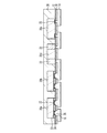
Classifications
-
- H—ELECTRICITY
- H05—ELECTRIC TECHNIQUES NOT OTHERWISE PROVIDED FOR
- H05K—PRINTED CIRCUITS; CASINGS OR CONSTRUCTIONAL DETAILS OF ELECTRIC APPARATUS; MANUFACTURE OF ASSEMBLAGES OF ELECTRICAL COMPONENTS
- H05K3/00—Apparatus or processes for manufacturing printed circuits
- H05K3/22—Secondary treatment of printed circuits
- H05K3/28—Applying non-metallic protective coatings
-
- H—ELECTRICITY
- H10—SEMICONDUCTOR DEVICES; ELECTRIC SOLID-STATE DEVICES NOT OTHERWISE PROVIDED FOR
- H10W—GENERIC PACKAGES, INTERCONNECTIONS, CONNECTORS OR OTHER CONSTRUCTIONAL DETAILS OF DEVICES COVERED BY CLASS H10
- H10W70/00—Package substrates; Interposers; Redistribution layers [RDL]
- H10W70/60—Insulating or insulated package substrates; Interposers; Redistribution layers
Definitions
- the present invention relates to a module and a manufacturing method thereof, for example, a module for mounting a semiconductor component and a manufacturing method thereof.
- voids or the like may be formed at the opening of the protective film.
- the present invention has been made in view of the above problems, and an object of the present invention is to suppress voids.
- the present invention provides a semiconductor component having a semiconductor layer having electrodes on its upper surface, a protective film provided on the semiconductor layer and having a first opening for exposing the electrodes, and a protective film provided on the protective film.
- An adhesive having a third opening that exposes the electrode and has a second opening larger than the first opening, an adhesive that adheres the protective film and the resin insulating layer, and exposes the electrode.
- This module is provided on a resin insulating layer and includes a metal layer in which the first opening, the second opening, and the third opening are embedded and connected to the electrode.
- all the outer circumferences of the second opening can be located outside the outer circumference of the first opening.
- At least a part of the adhesive may be provided on the side surface of the first opening.
- the planar shape of the electrode, the first opening and the second opening is substantially rectangular, and the electrode, the first opening and the second opening are adjacent to the side along the side of the semiconductor layer.
- the side of the second opening on the center side of the semiconductor layer may be located closer to the center of the semiconductor layer than the first opening.
- the metal layer can be thicker than the resin insulating layer.
- a recess is provided on the upper surface of the metal layer of the second opening, and the recess can be embedded by a conductive layer.
- a recess is provided on the upper surface of the metal layer of the second opening, and the resin insulating layer, the insulating layer provided on the metal layer, and the insulating layer are provided and penetrate the insulating layer.
- the configuration may include a wiring layer that connects to the metal layer at a location different from the recess through the fourth opening.
- a flexible resin insulating layer provided with a second opening that exposes a central portion located inside from the inside, and an upper surface of the semiconductor component provided on the lower surface of the resin insulating layer and adhere to the first opening.
- An adhesive having a third opening having an outer circumference located outside the outer circumference and inside the outer circumference of the second opening, and a stepped opening composed of the first opening, the second opening, and the third opening. It is a module including a metal layer that is in contact with the electrode and a conductive layer that fills a recess formed on the metal layer to flatten the upper surface.
- the metal layer can be configured by embedding a conductive paste in the recess and curing the metal layer.
- a semiconductor component provided with a semiconductor layer having an electrode on the upper surface and a protective film provided on the semiconductor layer and having a first opening for exposing the electrode is provided with a resin insulating layer via an adhesive.
- This is a method for manufacturing a module, which comprises a step of forming a first metal layer in which the first opening, the second opening and the third opening are embedded on the resin insulating layer and connected to the electrode. ..
- voids can be suppressed.
- FIG. 1 (a) to 1 (d) are cross-sectional views showing a method of manufacturing a module according to the first embodiment.
- FIG. 2 is a cross-sectional view of the module according to Comparative Example 1.
- 3 (a) and 3 (b) are cross-sectional views showing a method of manufacturing a module according to a modification 1 of the first embodiment.
- 4 (a) is a plan view of the module according to the second modification of the first embodiment
- FIG. 4 (b) is a cross-sectional view corresponding to AA of FIG. 4 (a).
- FIG. 5 is a plan view of the module according to Comparative Example 2.
- 6 (a) to 6 (c) are cross-sectional views of the module according to the third modification of the first embodiment.
- FIG. 7 is a cross-sectional view of the module according to Comparative Example 3.
- 8 (a) is a cross-sectional view of the module according to the second embodiment
- FIG. 8 (b) is a cross-sectional view of the module according to the first modification of the second embodiment.
- FIG. 9 is a cross-sectional view of the module according to the third embodiment.
- FIG. 10 is a cross-sectional view of the module according to the first modification of the third embodiment.
- the insulating adhesive 12 is applied to the lower surface of the insulating layer 10.
- the insulating layer 10 is a resin layer such as a polyimide layer and has flexibility.
- the thickness of the insulating layer 10 is, for example, 25 ⁇ m to 50 ⁇ m
- the adhesive 12 is a resin adhesive made of, for example, an epoxy resin.
- a spin coating method, a spray coating method, a screen printing method or an inkjet method is used.
- the thickness of the adhesive 12 is, for example, 5 ⁇ m to 20 ⁇ m after curing.
- openings 16a and 16b penetrating the insulating layer 10 and the adhesive 12 are formed.
- the openings 16a and 16b are formed, for example, by irradiating a laser beam.
- the size of the opening 16a is, for example, 30 ⁇ m to 500 ⁇ m.
- the semiconductor component 20 is arranged on the lower surface of the adhesive 12.
- the adhesive 12 is cured and the semiconductor component 20 and the insulating layer 10 are adhered to each other.
- the heat treatment is carried out at a temperature of, for example, 150 ° C to 300 ° C.
- the width D2 of the opening 16a of the insulating layer 10 and the width D3 of the opening 16b of the adhesive 12 are larger than the width D1 of the opening 26 of the protective film 24.
- the distance D4 between the end of the opening 26 of the protective film 24 and the end of the opening 16a of the insulating layer 10 is, for example, 1 ⁇ m to 100 ⁇ m, for example, 5 ⁇ m to 20 ⁇ m.
- the width D2 of the opening 16a is the width of the opening 16a on the lower surface of the insulating layer 10.
- the width D1 of the opening 26 is the width of the opening 26 on the upper surface of the protective film 24.
- the cross-sectional shape of the opening 16b may change when the adhesive 12 is softened by heat treatment.
- the smallest width of the opening 16b of the adhesive 12 is the width D3.
- the semiconductor component 20 is, for example, a transistor or diode such as an IGBT (Insulated Gate Bipolar Transistor), a bipolar transistor or a FET (Field Effect Transistor).
- a transistor or diode such as an IGBT (Insulated Gate Bipolar Transistor), a bipolar transistor or a FET (Field Effect Transistor).
- the transistor or diode a semiconductor made of Si, GaN, SiC or the like is used.
- the semiconductor component 20 includes a substrate 21 on which a transistor or a diode is formed, an electrode 22 provided on the upper surface of the substrate 21, and a protective film 24 having an opening 26 for exposing the electrode 22.
- the electrode 22 is provided on, for example, a protective film such as a silicon oxide film provided on the surface of the substrate 21.
- the substrate 21 includes a substrate 21a such as a sapphire substrate and a semiconductor layer 21b such as a GaN layer provided on the substrate 21a.
- a silicon-based substrate such as a power MOS (Metal Oxide Semiconductor) transistor or a bipolar transistor
- P-type and N-type diffusion layers are formed on the silicon substrate to form a horizontal or vertical type.
- a transistor is formed, and a silicon oxide film or a silicon nitride film is formed on the surface of the silicon substrate.
- An electrode 22 that is electrically connected to the diffusion layer is provided on the surface of the silicon substrate.
- the electrode 22 is, for example, a metal layer whose main material is gold, aluminum, copper, or the like.
- the protective film 24 is, for example, a resin insulating layer such as a polyimide resin, a silicon nitride film, or a glass-based inorganic insulating layer.
- the thickness of the substrate 21 is, for example, 50 ⁇ m to 200 ⁇ m, and the thickness of the protective film 24 is, for example, 1 ⁇ m to 20 ⁇ m.
- the metal layer 14 is formed on the insulating layer 10 and in the openings 16a, 16b and 26.
- the metal layer 14 contacts the electrode 22 through the openings 16a, 16b and 26.
- the metal layer 14 is formed by using, for example, copper as a main material and an electrolytic plating method.
- an adhesion layer mainly made of titanium or nickel and a seed layer mainly made of copper may be formed, and a metal layer may be formed on the seed layer.
- the thickness of the metal layer 14 is, for example, 20 ⁇ m to 100 ⁇ m. Since the metal layer 14 carries a large current, it may be thicker than the insulating layer 10.
- an adhesion layer and a metal layer are formed on the entire surface of the insulating layer 10 including the opening, and processed into a desired conductive pattern.
- the conductive pattern is composed of electrodes, pads, wiring, vias, or wiring integrated with the electrodes or pads.
- FIG. 2 is a cross-sectional view of the module according to Comparative Example 1.
- the width D2 of the opening 16a of the insulating layer 10 and the width D3 of the opening 16b of the adhesive 12 are smaller than the width D1 of the opening 26 of the protective film 24.
- the size of the opening 26 of the semiconductor component 20 is originally large, and the opening 16a opened in the insulating layer 10 is smaller than the opening 26.
- the opening 26 of the semiconductor component 20 is not provided and then the opening 26 is formed.
- openings 16a and 16b are formed in the insulating layer 10 and the adhesive 12, and the protective film 24 of the semiconductor component 20 is etched by using the insulating layer 10 and the adhesive 12 as masks.
- the etching is slightly overetched, the opening 26 becomes an overhang with respect to the openings 16a and 16b, and an eave is formed.
- the metal layer 14 may not be sufficiently filled in the opening 26, and a void 50 may be formed.
- the void 50 is formed, the resistance of the contact portion becomes relatively large. Since the semiconductor component 20 which is a transistor handles a large amount of electric power, the temperature may rise significantly, bubbles in the void may burst, and the mechanical and electrical reliability of the unfilled via portion may decrease.
- the semiconductor component 20 in which the opening 26 is formed in advance in the protective film 24 (resin insulating layer) which is a passivation film is prepared.
- the semiconductor component 20 is arranged on the insulating layer 10 and the adhesive 12 (resin insulating sheet) having openings 16a and 16b, and is aligned and fixed as shown in FIG. 1C.
- the electrodes 22 are exposed in the openings 16a and 16b of the insulating layer 10 and the adhesive 12.
- the insulating layer 10 has an opening 16a (second opening) larger than the opening 26 (first opening).
- the adhesive 12 has an opening 16b (third opening) that adheres the protective film 24 and the insulating layer 10 and exposes the electrode 22.
- this opening 16b is formed at the same time as the opening 16a by laser processing, it is the same as or smaller than the opening 16a and larger than the opening 26. Therefore, preferably, as shown in FIG. 1 (c), the surface of the protective film 24 appears with a slight width (interval D4) inside the opening 16b, and the opening 26 is further provided inside.
- the openings 26 and 16a and 16b have a stepped shape, and no eaves are provided.
- the adhesion layer and the metal layer 14 can be filled in a good state.
- the metal layer 14 (first metal layer) is provided on the insulating layer 10, and the openings 16a and 16b and the openings 26 are in contact with the embedded electrode 22. As a result, it is possible to suppress the formation of the void 50 and suppress the deterioration of the mechanical and electrical reliability of the via portion.
- the insulating layer 10 and the adhesive 12 are opened by one laser processing. Therefore, in laser processing, it is important that the outer circumferences of the opening 16a of the insulating layer 10 and the opening 16b of the adhesive 12 are located outside the outer circumference of the opening 26 of the protective film 24. Thereby, the formation of the void 50 can be further suppressed.
- [Modification 1 of Example 1] 3 (a) and 3 (b) are cross-sectional views showing a method of manufacturing a module according to a modification 1 of the first embodiment.
- the first embodiment is called a front via
- the modified example 1 of the first embodiment is called a rear via.
- the semiconductor component 20 having the opening 26 formed is bonded to the insulating layer 10 via the adhesive 12 after FIG. 1A of the first embodiment.
- openings 16a and 16b are formed in the insulating layer 10 and the adhesive 12.
- the adhesion layer and the metal layer 14 are coated and patterned.
- the openings 16a and 16b may be formed after the semiconductor component 20 is mounted on the insulating layer 10.
- a protective film 24 of the semiconductor component 20 having an opening 26 formed therein is prepared in advance, and an insulating layer 10 with an adhesive 12 is attached to the semiconductor component 20.
- the openings 16a and 16b are formed in the insulating layer 10 and the adhesive 12, and then the opening 26 is formed in the protective film 24 of the semiconductor component 20 as shown in FIG. 1 (c). May be formed.
- a method of forming the opening 26 in the protective film 24 by etching will be described.
- a mask having an opening smaller than the opening 16b and larger than the opening 26 to be formed is formed on the protective film 24.
- a mask is formed so as to cover the protective film 24 and the insulating layer 10, and an opening for etching is formed.
- the protective film 24 is etched through the opening of the mask to remove the mask.
- the opening 26 as shown in FIG. 1C is formed.
- the width D1 of the opening 26 is smaller than the width D3 of the opening 16b, and the protective film 24 is exposed between the opening 16b and the opening 26.
- FIG. 4 (a) is a plan view of the module according to the second modification of the first embodiment
- FIG. 4 (b) is a cross-sectional view corresponding to AA of FIG. 4 (a).
- the planar shape of the semiconductor component 20 is substantially rectangular.
- the semiconductor component 20 is, for example, 6 mm ⁇ 4 mm and has a thickness of 120 ⁇ m.
- Electrodes 22 are provided along the long sides of the semiconductor component 20.
- the opening 26 of the protective film 24 has a substantially rectangular shape, and the width D1 of the opening 26 is, for example, 650 ⁇ m.
- the opening 26 is provided on the electrode 22.
- the width D2 of the opening 16a of the insulating layer 10 is, for example, 700 ⁇ m, which is larger than D1.
- the end 52a of the opening 16a of the insulating layer 10 on the center side of the semiconductor component 20 is located on the protective film 24. That is, the end 52a of the opening 16a is located closer to the center of the semiconductor component 20 than the end 53a of the opening 26. However, the end 52b of the opening 16a on the outer peripheral side of the semiconductor component 20 is located inside the opening 26.
- the absolute value of the distance D4a between the end 52a of the opening 16a and the end 53a of the opening 26 on the central side of the semiconductor component 20 is the distance between the end 52b of the opening 16a and the end 53b of the opening 26 on the outside of the semiconductor component 20. Larger than D4b.
- the end 52b of the opening 16a is located in the opening 26, but the interval D4b can be reduced by making the width D2 of the opening 16a wider than the width D1 of the opening 26. Therefore, the generation of void 50 can be suppressed.
- the end 52b of the opening 16a is preferably provided outside the end 53b of the opening 26.
- the opening 16a may come off from the protective film 24. This may cause problems such as leakage of the plating solution when forming the metal layer 14, for example. Therefore, the end 52b of the opening 16a is provided inside the end 53b of the opening 26.
- the left opening 16a of FIG. 4B there is a slight eave on the left side of the opening 16a (outer peripheral side of the semiconductor component 20), but as it goes to the right, on the right side of the opening 16a (center side of the semiconductor component 20).
- the formation of the eaves is eliminated, and the openings 26 and 16a are formed in a stepped shape.
- the right opening 16a is the opposite.
- the upper side of the upper opening 26 and the lower side of the lower opening 26 have a small gap between them and the outer shape of the substrate 21a. This is to reduce the size of the semiconductor component 20 as much as possible.
- the opening 26 is elongated.
- FIG. 5 is a plan view of the module according to Comparative Example 2.
- a plurality of openings 16a of the insulating layer 10 are provided in the openings 26 of the semiconductor component 20.
- the diameter of the opening 16a is, for example, 400 ⁇ m.
- Comparative Example 2 since the eaves are formed between the openings 26 and 16a, voids are formed. Therefore, the mechanical and electrical reliability of the via portion may decrease.
- the second modification of the first embodiment at least a part of the outer circumference of the opening 16a of the insulating layer 10 is located outside the outer circumference of the opening 26 of the protective film 24.
- the formation of the void 50 can be suppressed.
- the void 50 can be further suppressed.
- the contact resistance electrical resistance and thermal resistance
- the planar shapes of the electrode 22, the opening 26 and 16a are substantially rectangular, and the electrode 22, the opening 26 and the opening 16a are provided adjacent to the side along the side (for example, the long side) of the semiconductor layer 21b.
- the side of the opening 16a on the center side of the semiconductor layer 21b is located closer to the center of the semiconductor layer 21b than the opening 26. Thereby, the formation of the void 50 can be suppressed.
- [Modification 3 of Example 1] 6 (a) to 6 (c) are cross-sectional views of the module according to the third modification of the first embodiment.
- the adhesive 12 when the adhesive 12 is heat-treated, the adhesive 12 may soften and have fluidity.
- the adhesive 12a of the adhesive 12 may cover the side surface of the opening 26.
- the width D3 of the opening 16b of the adhesive 12 is smaller than the width D1 of the opening 26 of the protective film 24.
- the side surface of the adhesive 12a is preferably forward tapered. As a result, the formation of void 50 is suppressed.
- the adhesive 12a may wet and spread on the upper surface of the protective film 24 without moving to the side surface of the opening 26.
- the width D3 of the opening 16b of the adhesive 12 is substantially the same as the width D1 of the opening 26 of the protective film 24.
- the adhesive 12 flows inside the width D1 or on the side wall of the opening 26.
- the adhesive 12a may spread to the side surface of the opening 26 even when the opening 16a is deviated from the opening 26 as in the modified example 2 of the first embodiment (left side). Aperture). Further, the adhesive 12a may wet and spread on the upper surface of the protective film 24 without moving to the side surface of the opening 26 (opening on the right side).
- FIG. 7 is a cross-sectional view of the module according to Comparative Example 3.
- the width D2 of the opening 16a of the insulating layer 10 is smaller than the width D1 of the opening 26 of the protective film 24.
- the void 50 is difficult to form when the adhesive 12 moves to the side surface of the protective film 24 and the opening 16b of the adhesive 12 becomes a forward taper.
- the width D2 of the opening 16a of the insulating layer 10 is small, even if the adhesive 12a spreads to the side surface of the protective film 24, it may have a reverse taper. In this case, the void 50 is formed between the adhesive 12a and the metal layer 14.
- the void 50 may be formed depending on the heat treatment condition or the type of the adhesive 12, and the void 50 may be formed. It may not be formed.
- Heat treatment is performed by making the width D2 of the opening 16a of the insulating layer 10 larger than the width D1 of the opening 26 of the protective film 24 as in the modified example 3 of the first embodiment (FIGS. 6A to 6C).
- the void 50 can be suppressed regardless of the situation of the above or the type of the adhesive 12.
- the relationship between the widths is D1 ⁇ D3 ⁇ D2.
- FIG. 8A is a cross-sectional view of the module according to the second embodiment.
- the openings 16a, 16b and 26 have a structure as shown in FIG. 1D, and no void is formed.
- the metal layer 14 cannot cover the opening 16a, and a recess 56 is formed on the upper surface of the metal layer 14. Therefore, voids may be formed in the recesses 56 when the metal layer 14 is mounted on the motherboard via solder. Therefore, the recess 56 can be made flat by embedding the recess 56 with the metal layer 18.
- the metal layer 18 is, for example, a conductive paste such as copper or silver paste in which copper particles or silver particles are dispersed in a resin paste, and is embedded in the recess 56.
- the metal layer 18 is a conductive layer obtained by curing a conductive paste by heat treatment.
- the recess 56 is provided on the upper surface of the metal layer 14 of the opening 16a.
- the recess 56 is embedded by a metal layer 18 (conductive layer).
- the recess 56 on the metal layer 14 can be flattened, and defects such as voids can be suppressed.
- the semiconductor component 20 has a transistor formed in the inner layer, an electrode 22 electrically connected to the transistor on the upper surface thereof, and an opening 26 (first opening) for exposing the electrode 22.
- a protective film 24 is provided.
- the insulating layer 10 (resin insulating layer) is provided with an opening 16a (second opening) that exposes a central portion located inside from the periphery of the electrode 22 of the semiconductor component 20.
- the adhesive 12 is provided on the lower surface of the insulating layer 10, adheres the upper surface of the semiconductor component 20, and has an outer circumference 16b (third opening) having an outer circumference located outside the outer circumference of the opening 26 and inside the outer circumference of the opening 16a. ).
- the metal layer 14 fills a stepped opening composed of openings 26, 16a and 16b and is in contact with the electrode 22.
- the metal layer 18 fills the recess 56 formed on the metal layer 14 to flatten the upper surface. As a result, voids and the like can be suppressed. Further, the metal layer 18 is obtained by embedding a conductive paste in the recess 56 and hardening the metal layer 18.
- FIG. 8B is a cross-sectional view of the module according to the first modification of the second embodiment.
- the insulating layer 30 is adhered onto the metal layer 14 via the adhesive 32.
- the recess 56 is embedded with the adhesive 32.
- An opening 36 is formed in the insulating layer 30 and the adhesive 32.
- a metal layer 34 for embedding the opening 36 is formed on the insulating layer 30.
- the adhesive 32 may be formed of a conductive paste as shown in FIG. 8A.
- the insulating layer 30 is provided on the insulating layer 10 and the metal layer 14.
- the metal layer 34 (wiring layer) is provided on the insulating layer 30 and is connected to the metal layer 14 at a position different from the recess 56 via an opening 36 (fourth opening) penetrating the insulating layer 30.
- FIG. 9 is a cross-sectional view of the module according to the third embodiment.
- the semiconductor parts 20a and 20b are mounted on the insulating layer 10 by using the adhesive 12 as in the first embodiment.
- the semiconductor component 20a is, for example, a GaN transistor or a SiC transistor.
- the semiconductor component 20b is a diode.
- the metal layer 14 functions as wiring and electrodes for electrically connecting the semiconductor components 20a and 20b.
- Metal layers 44 and 42 are provided on the upper surface and the lower surface of the insulating substrate 40.
- the insulating substrate 40 is, for example, a ceramic substrate.
- the metal layers 42 and 44 are, for example, copper layers.
- the upper surfaces of the semiconductor parts 20a and 20b are joined to the lower surface of the metal layer 42 by the bonding layer 46.
- the insulating substrate 40, the metal layers 42 and 44 function as a sheet sink that transiently stores the heat of the semiconductor parts 20a and 20b, and further functions as a heat radiating plate that releases heat to the outside.
- the bonding layer 46 is, for example, a resin adhesive, a conductive adhesive such as a metal paste, or a brazing material such as solder.
- a sealing member 48 is filled between the insulating layer 10 and the insulating substrate 40.
- the sealing member 48 is an insulator such as a resin (thermosetting resin such as epoxy resin or thermoplastic resin) and seals semiconductor parts 20a and 20b.
- a resin thermosetting resin such as epoxy resin or thermoplastic resin
- Other configurations are the same as those of Examples 1 and 2 and their modifications.
- FIG. 10 is a cross-sectional view of the module according to the first modification of the third embodiment. Similar to the third embodiment, the semiconductor parts 20a to 20c and the electronic parts 20d are adhered to the insulating layer 10 by using the adhesive 12.
- the semiconductor component 20a is, for example, a GaN transistor or a SiC transistor.
- the semiconductor component 20b is, for example, a diode.
- the semiconductor component 20c is, for example, an integrated circuit, and is a driver for driving power elements such as the semiconductor components 20a and 20b.
- the electronic component 20d is, for example, a discrete chip resistor, a chip capacitor and a chip inductor.
- the metal layer 14 is connected to the electrodes 22 of the semiconductor components 20a and 20b which are transistors, the semiconductor component 20c which is an integrated circuit, and the electronic component 20d, and constitutes a desired circuit. If necessary, a sealing member 38 is provided on the insulating layer 10 so as to cover the semiconductor parts 20a to 20c and the electronic parts 20d.
- the sealing member 38 is an insulator such as a resin. Other configurations are the same as those of Examples 1 and 2 and their modifications.
- a plurality of semiconductor parts 20a to 20c are provided, and the metal layer 14 electrically connects at least two electronic parts of the plurality of semiconductor parts 20a to 20c and the electronic parts 20d. Functions as wiring.
- the metal layer 14 is formed in the stepped openings 26 and 16a and 16b, so that the vicinity of the electrodes 22 of the semiconductor parts 20a to 20c is formed. The formation of the void 50 in the above can be suppressed.
Landscapes
- Engineering & Computer Science (AREA)
- Manufacturing & Machinery (AREA)
- Microelectronics & Electronic Packaging (AREA)
- Internal Circuitry In Semiconductor Integrated Circuit Devices (AREA)
Abstract
上面に電極が設けられた半導体層と、前記半導体層上に設けられ、前記電極を露出する第1開口を有する保護膜と、を備える半導体部品と、前記保護膜上に設けられ、前記電極を露出し前記第1開口より大きな第2開口を有する樹脂絶縁層と、前記保護膜と前記樹脂絶縁層とを接着し、前記電極を露出する第3開口を有する接着剤と、前記樹脂絶縁層上に設けられ、前記第1開口、前記第2開口および前記第3開口を埋め込み前記電極と接続する金属層と、を備えるモジュール。
Description
本発明はモジュールおよびその製造方法に関し、例えば半導体部品を搭載するモジュールおよびその製造方法に関する。
絶縁層の下面に接着剤を介し半導体部品を搭載し、絶縁層および接着剤を貫通する開口を介し絶縁層の上面から電子部品に接続する金属層を設けることが知られている(例えば特許文献1)。
しかしながら、半導体部品の電極上に開口を有する保護膜が設けられている場合、保護膜の開口においてボイド等が形成されることがある。
本発明は、上記課題に鑑みなされたものであり、ボイドを抑制することを目的とする。
本発明は、上面に電極が設けられた半導体層と、前記半導体層上に設けられ、前記電極を露出する第1開口を有する保護膜と、を備える半導体部品と、前記保護膜上に設けられ、前記電極を露出し前記第1開口より大きな第2開口を有する樹脂絶縁層と、前記保護膜と前記樹脂絶縁層とを接着し、前記電極を露出する第3開口を有する接着剤と、前記樹脂絶縁層上に設けられ、前記第1開口、前記第2開口および前記第3開口を埋め込み前記電極と接続する金属層と、を備えるモジュールである。
上記構成において、前記第2開口の外周は全て前記第1開口の外周より外側に位置する構成とすることができる。
上記構成において、前記接着剤の少なくとも一部は前記第1開口の側面に設けられる構成とすることができる。
上記構成において、前記電極、前記第1開口および前記第2開口の平面形状は略長方形であり、前記電極、前記第1開口および前記第2開口は前記半導体層の辺に沿い前記辺に隣接して設けられ、前記第2開口の前記半導体層の中心側の辺は前記第1開口より前記半導体層の中心側に位置する構成とすることができる。
上記構成において、前記金属層は前記樹脂絶縁層より厚い構成とすることができる。
上記構成において、前記第2開口の前記金属層の上面に凹部が設けられ、前記凹部は導電層により埋め込まれている構成とすることができる。
上記構成において、前記第2開口の前記金属層の上面に凹部が設けられ、前記樹脂絶縁層および前記金属層上に設けられた絶縁層と、前記絶縁層上に設けられ、前記絶縁層を貫通する第4開口を介し前記凹部と異なる箇所で前記金属層と接続する配線層と、を備える構成とすることができる。
本発明は、内層にトランジスタが形成され、上面にトランジスタと電気的に接続された電極が設けられ、前記電極を露出する第1開口を有する保護膜が設けられた半導体部品と、前記電極の周囲から内側に位置する中央部を露出する第2開口が設けられた可撓性の樹脂絶縁層と、前記樹脂絶縁層の下面に設けられ、前記半導体部品の上面を接着し、前記第1開口の外周よりも外側かつ前記第2開口の外周よりも内側に位置する外周を有する第3開口を有する接着剤と、前記第1開口、前記第2開口および前記第3開口からなるステップ状の開口部を埋め、前記電極と接触された金属層と、前記金属層上に形成された凹部を埋めて上面を平坦とする導電層とを備えるモジュールである。
上記構成において、前記金属層は、導電ペーストを前記凹部に埋設し、硬化されたものである構成とすることができる。
本発明は、上面に電極が設けられた半導体層と、前記半導体層上に設けられ、前記電極を露出する第1開口を有する保護膜と、を備える半導体部品を、接着剤を介し樹脂絶縁層の下面に接着する工程と、前記電極が露出するように、前記樹脂絶縁層に前記電極を露出し前記第1開口より大きな第2開口および前記接着剤に前記電極を露出する第3開口を形成する工程と、前記樹脂絶縁層上に、前記第1開口、前記第2開口および前記第3開口を埋め込み前記電極と接続する第1金属層を形成する工程と、を含むモジュールの製造方法である。
本発明によれば、ボイドを抑制することができる。
以下、図面を参照し本発明の実施例について説明する。
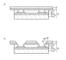
図1(a)から図1(d)は、実施例1に係るモジュールの製造方法を示す断面図である。図1(a)に示すように、絶縁層10の下面に絶縁性の接着剤12を塗布する。絶縁層10は例えばポリイミド層等の樹脂層であり、可撓性を有する。絶縁層10の厚さは例えば25μmから50μmであり、接着剤12は、例えばエポキシ樹脂等からなる樹脂接着剤である。接着剤12の塗布は、例えばスピンコート法、スプレコート法、スクリーン印刷法またはインクジェット法を用いる。接着剤12の厚さは硬化後で例えば5μmから20μmである。
図1(b)に示すように、絶縁層10および接着剤12を貫通する開口16aおよび16bを形成する。開口16aおよび16bは、例えばレーザ光を照射することにより形成する。開口16aの大きさは、例えば30μmから500μmである。
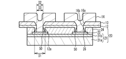
図1(c)に示すように、接着剤12の下面に半導体部品20を配置する。熱処理することにより、接着剤12を硬化させ半導体部品20と絶縁層10とを接着する。熱処理は例えば150℃から300℃の温度で実施する。絶縁層10の開口16aの幅D2および接着剤12の開口16bの幅D3は、保護膜24の開口26の幅D1より大きい。保護膜24の開口26の端と絶縁層10の開口16aの端との間隔D4は、例えば1μmから100μmであり、例えば5μmから20μmである。
開口16aの側面が傾斜している場合、開口16aの幅D2は絶縁層10の下面における開口16aの幅である。開口26の側面が傾斜している場合、開口26の幅D1は保護膜24の上面における開口26の幅である。開口16bの断面形状は、接着剤12が熱処理で軟化すると変わることがある。ここでは、接着剤12の開口16bの最も小さい幅を幅D3とする。
半導体部品20は、例えばIGBT(Insulated Gate Bipolar Transistor)、バイポーラトランジスタまたはFET(Field Effect Transistor)等のトランジスタまたはダイオードである。トランジスタまたはダイオードには、Si、GaNまたはSiC等を材料とする半導体が用いられる。半導体部品20は、トランジスタまたはダイオードが形成された基板21と、基板21の上面に設けられた電極22と、電極22を露出する開口26を有する保護膜24とを備える。電極22は、例えば基板21表面に設けられた酸化シリコン膜等の保護膜上に設けられている。例えば半導体部品20がGaNトランジスタの場合、基板21は、サファイア基板等の基板21aと基板21a上に設けられたGaN層等の半導体層21bを備える。例えば半導体部品20がパワーMOS(Metal Oxide Semiconductor)トランジスタまたはバイポーラトランジスタ等のシリコンを主材料とする基板を用いる場合、そのシリコン基板にP型およびN型の拡散層が形成され、横型または縦型のトランジスタが形成され、このシリコン基板の表面には、シリコン酸化膜またはシリコン窒化膜が形成されている。このシリコン基板の表面には、この拡散層と電気的に接続する電極22が設けられる。電極22は、例えば、金、アルミニウムまたは銅等を主材料とする金属層である。そして最表面には、一般にはパッシベーション膜と呼ばれる保護膜24が設けられる。この保護膜24は、例えばポリイミド樹脂等の樹脂絶縁層またはシリコン窒化膜もしくはガラス系の無機絶縁層である。基板21の厚さは例えば50μmから200μmであり、保護膜24の厚さは例えば1μmから20μmである。
図1(d)に示すように、絶縁層10上および開口16a、16bおよび26内に金属層14を形成する。金属層14は開口16a、16bおよび26を介し電極22に接触する。金属層14は例えば銅を主材料とし電解めっき法を用いて形成する。金属層14を形成する前に、チタンまたはニッケルを主材料とする密着層および銅を主材料とするシード層を形成し、シード層上に金属層を形成してもよい。金属層14の厚さは例えば20μmから100μmである。金属層14は大電流を流すため、絶縁層10より厚い場合もある。一般に、開口も含め絶縁層10の全面に、密着層と金属層が形成され、所望の導電パターンに加工される。なお、ここで導電パターンは、電極、パッド、配線、ビアまたは電極やパッドと一体の配線などで構成される。
[比較例1]
図2は、比較例1に係るモジュールの断面図である。図2に示すように、比較例1では、絶縁層10の開口16aの幅D2および接着剤12の開口16bの幅D3は保護膜24の開口26の幅D1より小さい。これには様々な要因がある。例えば半導体部品20の開口26のサイズがもともと大きく加工されており、開口26に対し絶縁層10に開けられた開口16aが小さい場合である。また例えば半導体部品20の開口26が設けられておらず、その後開口26を形成する場合である。絶縁層10および接着剤12に開口16aおよび16bが形成され、絶縁層10および接着剤12をマスクにして半導体部品20の保護膜24をエッチング加工する場合である。一般にはエッチングのときにややオーバーエッチングとするため、開口26は開口16aおよび16bに対しオーバーハングとなり、庇が形成される。
図2は、比較例1に係るモジュールの断面図である。図2に示すように、比較例1では、絶縁層10の開口16aの幅D2および接着剤12の開口16bの幅D3は保護膜24の開口26の幅D1より小さい。これには様々な要因がある。例えば半導体部品20の開口26のサイズがもともと大きく加工されており、開口26に対し絶縁層10に開けられた開口16aが小さい場合である。また例えば半導体部品20の開口26が設けられておらず、その後開口26を形成する場合である。絶縁層10および接着剤12に開口16aおよび16bが形成され、絶縁層10および接着剤12をマスクにして半導体部品20の保護膜24をエッチング加工する場合である。一般にはエッチングのときにややオーバーエッチングとするため、開口26は開口16aおよび16bに対しオーバーハングとなり、庇が形成される。
これにより、庇の部分は、開口26内に金属層14が十分に充填されず、ボイド50が形成される場合がある。ボイド50が形成されると、コンタクト部分の抵抗が比較的大きくなる。トランジスタである半導体部品20は、大電力を扱うため、大きく温度が上昇し、ボイド内の気泡が破裂したり、未充填のビア部の機械的および電気的な信頼性が低下することがある。
実施例1によれば、パッシベーション膜である保護膜24(樹脂絶縁層)に、予め開口26が形成された半導体部品20が用意される。続いて開口16aおよび16bが開けられた絶縁層10および接着剤12(樹脂絶縁シート)にこの半導体部品20が配置され、図1(c)のように位置合わせして固着される。その結果、絶縁層10および接着剤12の開口16aおよび16bには、電極22が露出する。絶縁層10は、開口26(第1開口)より大きな開口16a(第2開口)を有する。接着剤12は、保護膜24と絶縁層10とを接着し、電極22を露出する開口16b(第3開口)を有する。
この開口16bは、レーザ加工で開口16aと同時に形成されるため、開口16aと同じか、あるいは16aより小さく、開口26よりも大きい。よって好ましくは、図1(c)に示すように、開口16bの内側には、若干の幅(間隔D4)をもって保護膜24の表面が現れ、さらにその内側で開口26が設けられるとよい。
このように、断面図でみれば、開口26と16aおよび16bとは階段状となり、庇が設けられない。その結果、密着層、および金属層14は、良好な状態で充填が可能となる。金属層14(第1金属層)は、絶縁層10上に設けられ、開口16a、16bおよび開口26を埋め込み電極22と接触する。これにより、ボイド50が形成されることを抑制し、ビア部の機械的および電気的な信頼性の低下を抑制できる。
一般に、絶縁層10と接着剤12は一度のレーザ加工で開口される。よってレーザ加工では、絶縁層10の開口16aと接着剤12の開口16bの外周は保護膜24の開口26の外周より外側に位置させることが重要である。これにより、ボイド50の形成をより抑制できる。
[実施例1の変形例1]
図3(a)および図3(b)は、実施例1の変形例1に係るモジュールの製造方法を示す断面図である。実施例1は、先ビアと呼ばれ、実施例1の変形例1は、後ビアと呼ばれる。
図3(a)および図3(b)は、実施例1の変形例1に係るモジュールの製造方法を示す断面図である。実施例1は、先ビアと呼ばれ、実施例1の変形例1は、後ビアと呼ばれる。
ここでは、図3(a)に示すように、実施例1の図1(a)の後に絶縁層10に接着剤12を介して、開口26が形成された半導体部品20を接着している。そして、図3(b)に示すように、絶縁層10および接着剤12に開口16aおよび16bを形成する。その後、密着層、金属層14を被膜しパターニングする。この実施例1の変形例1のように、開口16aおよび16bは半導体部品20を絶縁層10に搭載した後に形成してもよい。
図3(a)では予め半導体部品20の保護膜24に開口26が形成されたものが用意され、接着剤12付きの絶縁層10が半導体部品20に貼られている。しかし接着剤12付きの絶縁層10を貼ってから、絶縁層10と接着剤12に開口16aおよび16bを形成し、その後、半導体部品20の保護膜24に図1(c)のように開口26を形成してもよい。
保護膜24に開口26をエッチングにより形成する方法を説明する。開口16bより小さく形成予定の開口26より大きな開口を有するマスクを保護膜24上に形成する。例えば保護膜24および絶縁層10上を覆うようにマスクを形成し、上記エッチング用の開口を形成する。そしてマスクの開口を介して保護膜24をエッチングし、マスクを除去する。これにより、図1(c)のような開口26が形成される。開口26の幅D1は開口16bの幅D3より小さくなり、開口16bと開口26との間に、保護膜24が露出する。
[実施例1の変形例2]
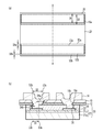
図4(a)は、実施例1の変形例2に係るモジュールの平面図、図4(b)は、図4(a)のA-Aに相当する断面図である。図4(a)および図4(b)に示すように、半導体部品20の平面形状は略長方形である。半導体部品20は例えば6mm×4mmであり、厚さは120μmである。半導体部品20の長辺に沿って電極22が設けられている。保護膜24の開口26は略長方形状であり、開口26の幅D1は例えば650μmである。開口26は電極22上に設けられている。絶縁層10の開口16aの幅D2は例えば700μmでありD1より大きい。
図4(a)は、実施例1の変形例2に係るモジュールの平面図、図4(b)は、図4(a)のA-Aに相当する断面図である。図4(a)および図4(b)に示すように、半導体部品20の平面形状は略長方形である。半導体部品20は例えば6mm×4mmであり、厚さは120μmである。半導体部品20の長辺に沿って電極22が設けられている。保護膜24の開口26は略長方形状であり、開口26の幅D1は例えば650μmである。開口26は電極22上に設けられている。絶縁層10の開口16aの幅D2は例えば700μmでありD1より大きい。
半導体部品20の中心側の絶縁層10の開口16aの端52aは保護膜24上に位置する。すなわち開口16aの端52aは開口26の端53aより半導体部品20の中心側に位置する。しかし、半導体部品20の外周側の開口16aの端52bは開口26の内側に位置する。これにより、半導体部品20の中心側における開口16aの端52aと開口26の端53aとの間隔D4aの絶対値は、半導体部品20の外側における開口16aの端52bと開口26の端53bとの間隔D4bより大きい。実施例1の変形例2においては、開口16aの端52bは開口26内に位置するが、開口16aの幅D2を開口26の幅D1より広くすることで、間隔D4bを小さくできる。このため、ボイド50の発生を抑制できる。開口16aの端52bは開口26の端53bより外側に設けることが好ましい。
しかし、開口16aが大きくなりすぎると、開口16aが保護膜24から外れてしまうことがある。これにより、例えば金属層14を形成するときにめっき液が漏れるなどの問題が生じることがある。そこで、開口16aの端52bを開口26の端53bより内側に設けている。
図4(b)の左の開口16aにおいて、開口16aの左側(半導体部品20の外周側)に若干の庇があるが、右に向かうにつれて、開口16aの右側(半導体部品20の中心側)では庇の形成はなくなり、開口26と16aは階段状に形成される。また右の開口16aはその逆となる。図4(a)に示すように、上の開口26の上側側辺および下の開口26の下側側辺は、基板21aの外形との間の隙間が小さい。これは半導体部品20のサイズをできるだけ小さくするためである。この開口26は細長く形成される。上の開口26の上側側辺および下の開口26の下側側辺に若干の庇が形成されるものの、上下の開口16aが半導体部品20の中心側に寄っているため、開口16aと26とを位置合わせするときに開口16aが開口26からずれても、金属層14を形成するためのめっき液が漏れることを抑制できる。
[比較例2]
図5は、比較例2に係るモジュールの平面図である。図5に示すように、比較例2では、絶縁層10の開口16aは半導体部品20の開口26内に複数個設けられている。開口16aの直径は例えば400μmである。比較例2では、開口26と16aとに間に庇が形成されるため、ボイドが形成される。よって、ビア部の機械的および電気的な信頼性の低下する可能性がある。
図5は、比較例2に係るモジュールの平面図である。図5に示すように、比較例2では、絶縁層10の開口16aは半導体部品20の開口26内に複数個設けられている。開口16aの直径は例えば400μmである。比較例2では、開口26と16aとに間に庇が形成されるため、ボイドが形成される。よって、ビア部の機械的および電気的な信頼性の低下する可能性がある。
実施例1の変形例2によれば、絶縁層10の開口16aの外周の少なくとも一部は保護膜24の開口26の外周より外側に位置する。これにより、ボイド50の形成を抑制できる。さらに、1つの開口26に1つの開口16aを設けることで、ボイド50をより抑制できる。また、金属層14と電極22との接触面積は大きくなるため、接触抵抗(電気抵抗および熱抵抗)を低くできる。
電極22、開口26および16aの平面形状は略長方形であり、電極22、開口26および開口16aは半導体層21bの辺(例えば長辺)に沿い辺に隣接して設けられている。開口16aの半導体層21bの中心側の辺は開口26より半導体層21bの中心側に位置する。これにより、ボイド50の形成を抑制できる。
[実施例1の変形例3]
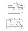
図6(a)から図6(c)は、実施例1の変形例3に係るモジュールの断面図である。実施例1の図1(c)において、接着剤12を熱処理すると接着剤12が軟化し流動性を有することがある。図6(a)に示すように、接着剤12の少なくとも一部の接着剤12aは開口26の側面を覆っていてもよい。この場合、接着剤12の開口16bの幅D3は保護膜24の開口26の幅D1より小さくなる。接着剤12aの側面は順テーパであることが好ましい。これにより、ボイド50の形成が抑制される。
図6(a)から図6(c)は、実施例1の変形例3に係るモジュールの断面図である。実施例1の図1(c)において、接着剤12を熱処理すると接着剤12が軟化し流動性を有することがある。図6(a)に示すように、接着剤12の少なくとも一部の接着剤12aは開口26の側面を覆っていてもよい。この場合、接着剤12の開口16bの幅D3は保護膜24の開口26の幅D1より小さくなる。接着剤12aの側面は順テーパであることが好ましい。これにより、ボイド50の形成が抑制される。
図6(b)に示すように、接着剤12aは開口26の側面まで移動しなくとも、保護膜24の上面に濡れ広がってもよい。この場合、接着剤12の開口16bの幅D3は保護膜24の開口26の幅D1と略同じとなる。または接着剤12は幅D1よりも内側か、開口26の側壁に流れる。
図6(c)に示すように、実施例1の変形例2のように、開口16aが開口26に対してずれている場合においても接着剤12aが開口26の側面まで広がってもよい(左側の開口)。また、接着剤12aは開口26の側面まで移動しなくとも、保護膜24の上面に濡れ広がってもよい(右側の開口)。
[比較例3]
図7は、比較例3に係るモジュールの断面図である。図7に示すように、比較例3では、絶縁層10の開口16aの幅D2は保護膜24の開口26の幅D1より小さい。接着剤12aに流動性がある場合、接着剤12が保護膜24の側面まで移動し、接着剤12の開口16bが順テーパとなるとボイド50は形成されにくい。しかしながら、絶縁層10の開口16aの幅D2が小さいと、接着剤12aが保護膜24の側面まで広がっても逆テーパとなることがある。この場合、接着剤12aと金属層14との間にボイド50が形成される。
図7は、比較例3に係るモジュールの断面図である。図7に示すように、比較例3では、絶縁層10の開口16aの幅D2は保護膜24の開口26の幅D1より小さい。接着剤12aに流動性がある場合、接着剤12が保護膜24の側面まで移動し、接着剤12の開口16bが順テーパとなるとボイド50は形成されにくい。しかしながら、絶縁層10の開口16aの幅D2が小さいと、接着剤12aが保護膜24の側面まで広がっても逆テーパとなることがある。この場合、接着剤12aと金属層14との間にボイド50が形成される。
接着剤12が流動性を有する場合には、開口16aの幅D2が開口26の幅D1より小さくても、熱処理の状況または接着剤12の種類によりボイド50が形成される場合と、ボイド50が形成されない場合がある。実施例1の変形例3(図6(a)から図6(c))のように、絶縁層10の開口16aの幅D2を保護膜24の開口26の幅D1より大きくすることで、熱処理の状況または接着剤12の種類によらず、ボイド50を抑制することができる。実施例1およびその変形例のように、各幅の関係はD1<D3≦D2となる。
図8(a)は、実施例2に係るモジュールの断面図である。開口16a、16bおよび26は図1(d)のような構造であり、ボイドは形成されない。しかし、図8(a)に示すように、絶縁層10の開口16aを大きくすると、金属層14が開口16aを覆うことができず、金属層14の上面に凹部56が形成される。そのため、金属層14を半田を介して、マザーボードへ実装するときに凹部56にボイドが形成されることがある。そこで、凹部56を金属層18で埋め込むことにより、凹部56を平坦にできる。金属層18は、例えば銅粒子または銀粒子を樹脂ペーストに分散させた銅または銀ペースト等の導電性ペーストであり、凹部56内に埋め込まれている。金属層18は、導電性ペーストを熱処理により硬化させた導電層である。
実施例2によれば、開口16aの金属層14の上面に凹部56が設けられている。凹部56は金属層18(導電層)により埋め込まれている。これにより、金属層14上の凹部56を平坦化でき、ボイド等の欠陥を抑制できる。
実施例2によれば、半導体部品20には、内層にトランジスタが形成され、上面にトランジスタと電気的に接続された電極22が設けられ、電極22を露出する開口26(第1開口)を有する保護膜24が設けられている。絶縁層10(樹脂絶縁層)には、半導体部品20の電極22の周囲から内側に位置する中央部を露出する開口16a(第2開口)が設けられている。接着剤12は、絶縁層10の下面に設けられ、半導体部品20の上面を接着し、開口26の外周よりも外側かつ開口16aの外周よりも内側に位置する外周を有する開口16b(第3開口)を有する。金属層14は、開口26、16aおよび16bからなるステップ状の開口部を埋め、電極22と接触されている。金属層18は、金属層14上に形成された凹部56を埋めて上面を平坦とする。これにより、ボイド等を抑制できる。また、金属層18は、導電ペーストを凹部56に埋設し、硬化されたものである。
[実施例2の変形例1]
図8(b)は、実施例2の変形例1に係るモジュールの断面図である。図8(b)に示すように、金属層14上に接着剤32を介し絶縁層30を接着する。これにより、凹部56は接着剤32により埋め込まれる。絶縁層30および接着剤32に開口36を形成する。絶縁層30上に開口36を埋め込む金属層34を形成する。なお、この接着剤32は、図8(a)のように、導電ペーストにより形成してもよい。
図8(b)は、実施例2の変形例1に係るモジュールの断面図である。図8(b)に示すように、金属層14上に接着剤32を介し絶縁層30を接着する。これにより、凹部56は接着剤32により埋め込まれる。絶縁層30および接着剤32に開口36を形成する。絶縁層30上に開口36を埋め込む金属層34を形成する。なお、この接着剤32は、図8(a)のように、導電ペーストにより形成してもよい。
実施例2の変形例1によれば、絶縁層30は絶縁層10および金属層14上に設けられている。金属層34(配線層)は、絶縁層30上に設けられ、絶縁層30を貫通する開口36(第4開口)を介し凹部56と異なる箇所で金属層14と接続する。このように、金属層34を用い再配線することで、凹部56の影響を低減できる。
図9は、実施例3に係るモジュールの断面図である。図9に示すように、実施例1と同様に、絶縁層10上に接着剤12を用い半導体部品20aおよび20bを搭載する。半導体部品20aは例えばGaNトランジスタまたはSiCトランジスタである。半導体部品20bはダイオードである。金属層14は、半導体部品20aと20bとを電気的に接続する配線および電極として機能する。
絶縁基板40の上面および下面には金属層44および42が設けられている。絶縁基板40は、例えばセラミックス基板である。金属層42および44は例えば銅層である。紙面において、半導体部品20aおよび20bの上面は接合層46により金属層42の下面に接合されている。絶縁基板40、金属層42および44は半導体部品20aおよび20bの熱を過渡的に貯めるシートシンクとして機能し、更には外部に熱を放出する放熱板として機能する。接合層46は、例えば樹脂接着剤、金属ペースト等の導電性接着剤、または半田等のロウ材である。絶縁層10と絶縁基板40との間は封止部材48が充填されている。封止部材48は、例えば樹脂(エポキシ樹脂等の熱硬化性樹脂または熱可塑性樹脂)等の絶縁体であり半導体部品20aおよび20bを封止する。その他の構成は実施例1から2およびその変形例と同じである。
[実施例3の変形例1]
図10は、実施例3の変形例1に係るモジュールの断面図である。実施例3と同様に、絶縁層10上に接着剤12を用い半導体部品20aから20cおよび電子部品20dが接着されている。半導体部品20aは例えばGaNトランジスタまたはSiCトランジスタである。半導体部品20bは例えばダイオードである。半導体部品20cは例えば集積回路であり、半導体部品20aおよび20b等のパワー素子を駆動するドライバである。電子部品20dは例えばディスクリートのチップ抵抗、チップコンデンサおよびチップインダクタである。金属層14は、トランジスタである半導体部品20a、20b、集積回路である半導体部品20cおよび電子部品20dの電極22に接続され、所望の回路を構成している。なお、必要により、絶縁層10上に半導体部品20aから20cおよび電子部品20dを覆うように封止部材38が設けられている。封止部材38は、例えば樹脂等の絶縁体である。その他の構成は実施例1から2およびその変形例と同じである。
図10は、実施例3の変形例1に係るモジュールの断面図である。実施例3と同様に、絶縁層10上に接着剤12を用い半導体部品20aから20cおよび電子部品20dが接着されている。半導体部品20aは例えばGaNトランジスタまたはSiCトランジスタである。半導体部品20bは例えばダイオードである。半導体部品20cは例えば集積回路であり、半導体部品20aおよび20b等のパワー素子を駆動するドライバである。電子部品20dは例えばディスクリートのチップ抵抗、チップコンデンサおよびチップインダクタである。金属層14は、トランジスタである半導体部品20a、20b、集積回路である半導体部品20cおよび電子部品20dの電極22に接続され、所望の回路を構成している。なお、必要により、絶縁層10上に半導体部品20aから20cおよび電子部品20dを覆うように封止部材38が設けられている。封止部材38は、例えば樹脂等の絶縁体である。その他の構成は実施例1から2およびその変形例と同じである。
実施例3およびその変形例1のモジュールでは、半導体部品20aから20cが複数設けられ、金属層14は複数の半導体部品20aから20cおよび電子部品20dのうち少なくとも2つの電子部品を電気的に接続する配線として機能する。実施例3およびその変形例1では、実施例1,2およびその変形例と同様に、ステップ状の開口26と16aおよび16bに金属層14を形成するため、半導体部品20aから20cの電極22付近におけるボイド50の形成を抑制できる。
以上、本発明の実施例について詳述したが、本発明はかかる特定の実施例に限定されるものではなく、特許請求の範囲に記載された本発明の要旨の範囲内において、種々の変形・変更が可能である。
10、30 絶縁層
12、12a、32 接着剤
14、34 金属層
16a、16b、26 開口
20、20a-20c 半導体部品
20d 電子部品
21a 基板
21b半導体層
22 電極
24 保護膜
12、12a、32 接着剤
14、34 金属層
16a、16b、26 開口
20、20a-20c 半導体部品
20d 電子部品
21a 基板
21b半導体層
22 電極
24 保護膜
Claims (10)
- 上面に電極が設けられた半導体層と、前記半導体層上に設けられ、前記電極を露出する第1開口を有する保護膜と、を備える半導体部品と、
前記保護膜上に設けられ、前記電極を露出し前記第1開口より大きな第2開口を有する樹脂絶縁層と、
前記保護膜と前記樹脂絶縁層とを接着し、前記電極を露出する第3開口を有する接着剤と、
前記樹脂絶縁層上に設けられ、前記第1開口、前記第2開口および前記第3開口を埋め込み前記電極と接続する金属層と、
を備えるモジュール。 - 前記第2開口の外周は全て前記第1開口の外周より外側に位置する請求項1に記載のモジュール。
- 前記接着剤の少なくとも一部は前記第1開口の側面に設けられる請求項1または2に記載のモジュール。
- 前記電極、前記第1開口および前記第2開口の平面形状は略長方形であり、前記電極、前記第1開口および前記第2開口は前記半導体層の辺に沿い前記辺に隣接して設けられ、前記第2開口の前記半導体層の中心側の辺は前記第1開口より前記半導体層の中心側に位置する請求項1から3のいずれか一項に記載のモジュール。
- 前記金属層は前記樹脂絶縁層より厚い請求項1から4のいずれか一項に記載のモジュール。
- 前記第2開口の前記金属層の上面に凹部が設けられ、
前記凹部は導電層により埋め込まれている請求項1から5いずれか一項に記載のモジュール。 - 前記第2開口の前記金属層の上面に凹部が設けられ、
前記樹脂絶縁層および前記金属層上に設けられた絶縁層と、
前記絶縁層上に設けられ、前記絶縁層を貫通する第4開口を介し前記凹部と異なる箇所で前記金属層と接続する配線層と、
を備える請求項1から5のいずれか一項に記載のモジュール。 - 内層にトランジスタが形成され、上面にトランジスタと電気的に接続された電極が設けられ、前記電極を露出する第1開口を有する保護膜が設けられた半導体部品と、
前記電極の周囲から内側に位置する中央部を露出する第2開口が設けられた可撓性の樹脂絶縁層と、
前記樹脂絶縁層の下面に設けられ、前記半導体部品の上面を接着し、前記第1開口の外周よりも外側かつ前記第2開口の外周よりも内側に位置する外周を有する第3開口を有する接着剤と、
前記第1開口、前記第2開口および前記第3開口からなるステップ状の開口部を埋め、前記電極と接触された金属層と、
前記金属層上に形成された凹部を埋めて上面を平坦とする導電層とを備えるモジュール。 - 前記導電層は、導電ペーストを前記凹部に埋設し、硬化されたものである請求項8に記載のモジュール。
- 上面に電極が設けられた半導体層と、前記半導体層上に設けられ、前記電極を露出する第1開口を有する保護膜と、を備える半導体部品を、接着剤を介し樹脂絶縁層の下面に接着する工程と、
前記電極が露出するように、前記樹脂絶縁層に前記電極を露出し前記第1開口より大きな第2開口および前記接着剤に前記電極を露出する第3開口を形成する工程と、
前記樹脂絶縁層上に、前記第1開口、前記第2開口および前記第3開口を埋め込み前記電極と接続する第1金属層を形成する工程と、
を含むモジュールの製造方法。
Applications Claiming Priority (2)
| Application Number | Priority Date | Filing Date | Title |
|---|---|---|---|
| JP2019064998 | 2019-03-28 | ||
| JP2019-064998 | 2019-03-28 |
Publications (1)
| Publication Number | Publication Date |
|---|---|
| WO2020195451A1 true WO2020195451A1 (ja) | 2020-10-01 |
Family
ID=72609228
Family Applications (1)
| Application Number | Title | Priority Date | Filing Date |
|---|---|---|---|
| PCT/JP2020/007331 Ceased WO2020195451A1 (ja) | 2019-03-28 | 2020-02-25 | モジュールおよびその製造方法 |
Country Status (1)
| Country | Link |
|---|---|
| WO (1) | WO2020195451A1 (ja) |
Cited By (1)
| Publication number | Priority date | Publication date | Assignee | Title |
|---|---|---|---|---|
| CN116110842A (zh) * | 2023-02-21 | 2023-05-12 | 上海华虹宏力半导体制造有限公司 | 一种半导体结构及其制备方法 |
Citations (5)
| Publication number | Priority date | Publication date | Assignee | Title |
|---|---|---|---|---|
| JP2002064162A (ja) * | 2000-08-21 | 2002-02-28 | Ibiden Co Ltd | 半導体チップ |
| JP2006286690A (ja) * | 2005-03-31 | 2006-10-19 | Casio Comput Co Ltd | 半導体装置およびその製造方法 |
| JP2009064914A (ja) * | 2007-09-05 | 2009-03-26 | Toshiba Corp | 半導体装置及び半導体装置の製造方法 |
| JP2012023409A (ja) * | 2011-10-31 | 2012-02-02 | Sanyo Electric Co Ltd | 回路装置およびその製造方法 |
| JP2012227444A (ja) * | 2011-04-21 | 2012-11-15 | Sumitomo Bakelite Co Ltd | 半導体装置の製造方法および半導体装置 |
-
2020
- 2020-02-25 WO PCT/JP2020/007331 patent/WO2020195451A1/ja not_active Ceased
Patent Citations (5)
| Publication number | Priority date | Publication date | Assignee | Title |
|---|---|---|---|---|
| JP2002064162A (ja) * | 2000-08-21 | 2002-02-28 | Ibiden Co Ltd | 半導体チップ |
| JP2006286690A (ja) * | 2005-03-31 | 2006-10-19 | Casio Comput Co Ltd | 半導体装置およびその製造方法 |
| JP2009064914A (ja) * | 2007-09-05 | 2009-03-26 | Toshiba Corp | 半導体装置及び半導体装置の製造方法 |
| JP2012227444A (ja) * | 2011-04-21 | 2012-11-15 | Sumitomo Bakelite Co Ltd | 半導体装置の製造方法および半導体装置 |
| JP2012023409A (ja) * | 2011-10-31 | 2012-02-02 | Sanyo Electric Co Ltd | 回路装置およびその製造方法 |
Cited By (1)
| Publication number | Priority date | Publication date | Assignee | Title |
|---|---|---|---|---|
| CN116110842A (zh) * | 2023-02-21 | 2023-05-12 | 上海华虹宏力半导体制造有限公司 | 一种半导体结构及其制备方法 |
Similar Documents
| Publication | Publication Date | Title |
|---|---|---|
| CN100487931C (zh) | 半导体发光元件及其制造方法和安装方法、发光器件 | |
| US9192049B2 (en) | Wiring substrate and semiconductor package | |
| JP5141076B2 (ja) | 半導体装置 | |
| JP4516320B2 (ja) | Led基板 | |
| JP6724449B2 (ja) | 半導体装置および半導体装置の製造方法 | |
| CN101447541A (zh) | 半导体器件 | |
| JP2006128455A (ja) | 半導体装置およびその製造方法 | |
| CN105575936B (zh) | 制造电路载体方法及制造和运行半导体装置的方法 | |
| CN107039364B (zh) | 半导体封装件及其制造方法 | |
| JP6392163B2 (ja) | 配線基板及びその製造方法、半導体装置 | |
| WO2018173511A1 (ja) | 半導体装置 | |
| US10424542B2 (en) | Semiconductor device | |
| TW201340261A (zh) | 半導體裝置及其製造方法 | |
| WO2020195451A1 (ja) | モジュールおよびその製造方法 | |
| JP2025061781A (ja) | 半導体装置 | |
| JP2020077857A (ja) | モジュールおよびその製造方法 | |
| TW201705439A (zh) | 半導體裝置 | |
| US20220285301A1 (en) | Semiconductor module and method of manufacturing semiconductor module | |
| JP2020155640A (ja) | モジュールおよびその製造方法 | |
| JPH05243287A (ja) | 混成集積回路装置およびその製造方法 | |
| JPH1027767A (ja) | 半導体装置の製造方法 | |
| WO2020202972A1 (ja) | モジュールおよびその製造方法 | |
| JP6989632B2 (ja) | 半導体装置 | |
| JP2020107685A (ja) | 半導体モジュール | |
| WO2018220868A1 (ja) | 半導体装置および半導体装置の製造方法 |
Legal Events
| Date | Code | Title | Description |
|---|---|---|---|
| 121 | Ep: the epo has been informed by wipo that ep was designated in this application |
Ref document number: 20779542 Country of ref document: EP Kind code of ref document: A1 |
|
| NENP | Non-entry into the national phase |
Ref country code: DE |
|
| 122 | Ep: pct application non-entry in european phase |
Ref document number: 20779542 Country of ref document: EP Kind code of ref document: A1 |
|
| NENP | Non-entry into the national phase |
Ref country code: JP |