WO2020195355A1 - 下地基板 - Google Patents
下地基板 Download PDFInfo
- Publication number
- WO2020195355A1 WO2020195355A1 PCT/JP2020/006312 JP2020006312W WO2020195355A1 WO 2020195355 A1 WO2020195355 A1 WO 2020195355A1 JP 2020006312 W JP2020006312 W JP 2020006312W WO 2020195355 A1 WO2020195355 A1 WO 2020195355A1
- Authority
- WO
- WIPO (PCT)
- Prior art keywords
- layer
- alignment layer
- base substrate
- region
- substrate
- Prior art date
- Legal status (The legal status is an assumption and is not a legal conclusion. Google has not performed a legal analysis and makes no representation as to the accuracy of the status listed.)
- Ceased
Links
Images


Classifications
-
- C—CHEMISTRY; METALLURGY
- C30—CRYSTAL GROWTH
- C30B—SINGLE-CRYSTAL GROWTH; UNIDIRECTIONAL SOLIDIFICATION OF EUTECTIC MATERIAL OR UNIDIRECTIONAL DEMIXING OF EUTECTOID MATERIAL; REFINING BY ZONE-MELTING OF MATERIAL; PRODUCTION OF A HOMOGENEOUS POLYCRYSTALLINE MATERIAL WITH DEFINED STRUCTURE; SINGLE CRYSTALS OR HOMOGENEOUS POLYCRYSTALLINE MATERIAL WITH DEFINED STRUCTURE; AFTER-TREATMENT OF SINGLE CRYSTALS OR A HOMOGENEOUS POLYCRYSTALLINE MATERIAL WITH DEFINED STRUCTURE; APPARATUS THEREFOR
- C30B25/00—Single-crystal growth by chemical reaction of reactive gases, e.g. chemical vapour-deposition growth
- C30B25/02—Epitaxial-layer growth
- C30B25/18—Epitaxial-layer growth characterised by the substrate
- C30B25/183—Epitaxial-layer growth characterised by the substrate being provided with a buffer layer, e.g. a lattice matching layer
-
- C—CHEMISTRY; METALLURGY
- C30—CRYSTAL GROWTH
- C30B—SINGLE-CRYSTAL GROWTH; UNIDIRECTIONAL SOLIDIFICATION OF EUTECTIC MATERIAL OR UNIDIRECTIONAL DEMIXING OF EUTECTOID MATERIAL; REFINING BY ZONE-MELTING OF MATERIAL; PRODUCTION OF A HOMOGENEOUS POLYCRYSTALLINE MATERIAL WITH DEFINED STRUCTURE; SINGLE CRYSTALS OR HOMOGENEOUS POLYCRYSTALLINE MATERIAL WITH DEFINED STRUCTURE; AFTER-TREATMENT OF SINGLE CRYSTALS OR A HOMOGENEOUS POLYCRYSTALLINE MATERIAL WITH DEFINED STRUCTURE; APPARATUS THEREFOR
- C30B23/00—Single-crystal growth by condensing evaporated or sublimed materials
-
- C—CHEMISTRY; METALLURGY
- C30—CRYSTAL GROWTH
- C30B—SINGLE-CRYSTAL GROWTH; UNIDIRECTIONAL SOLIDIFICATION OF EUTECTIC MATERIAL OR UNIDIRECTIONAL DEMIXING OF EUTECTOID MATERIAL; REFINING BY ZONE-MELTING OF MATERIAL; PRODUCTION OF A HOMOGENEOUS POLYCRYSTALLINE MATERIAL WITH DEFINED STRUCTURE; SINGLE CRYSTALS OR HOMOGENEOUS POLYCRYSTALLINE MATERIAL WITH DEFINED STRUCTURE; AFTER-TREATMENT OF SINGLE CRYSTALS OR A HOMOGENEOUS POLYCRYSTALLINE MATERIAL WITH DEFINED STRUCTURE; APPARATUS THEREFOR
- C30B29/00—Single crystals or homogeneous polycrystalline material with defined structure characterised by the material or by their shape
- C30B29/10—Inorganic compounds or compositions
- C30B29/16—Oxides
-
- C—CHEMISTRY; METALLURGY
- C30—CRYSTAL GROWTH
- C30B—SINGLE-CRYSTAL GROWTH; UNIDIRECTIONAL SOLIDIFICATION OF EUTECTIC MATERIAL OR UNIDIRECTIONAL DEMIXING OF EUTECTOID MATERIAL; REFINING BY ZONE-MELTING OF MATERIAL; PRODUCTION OF A HOMOGENEOUS POLYCRYSTALLINE MATERIAL WITH DEFINED STRUCTURE; SINGLE CRYSTALS OR HOMOGENEOUS POLYCRYSTALLINE MATERIAL WITH DEFINED STRUCTURE; AFTER-TREATMENT OF SINGLE CRYSTALS OR A HOMOGENEOUS POLYCRYSTALLINE MATERIAL WITH DEFINED STRUCTURE; APPARATUS THEREFOR
- C30B29/00—Single crystals or homogeneous polycrystalline material with defined structure characterised by the material or by their shape
- C30B29/10—Inorganic compounds or compositions
- C30B29/40—AIIIBV compounds wherein A is B, Al, Ga, In or Tl and B is N, P, As, Sb or Bi
- C30B29/403—AIII-nitrides
- C30B29/406—Gallium nitride
-
- C—CHEMISTRY; METALLURGY
- C30—CRYSTAL GROWTH
- C30B—SINGLE-CRYSTAL GROWTH; UNIDIRECTIONAL SOLIDIFICATION OF EUTECTIC MATERIAL OR UNIDIRECTIONAL DEMIXING OF EUTECTOID MATERIAL; REFINING BY ZONE-MELTING OF MATERIAL; PRODUCTION OF A HOMOGENEOUS POLYCRYSTALLINE MATERIAL WITH DEFINED STRUCTURE; SINGLE CRYSTALS OR HOMOGENEOUS POLYCRYSTALLINE MATERIAL WITH DEFINED STRUCTURE; AFTER-TREATMENT OF SINGLE CRYSTALS OR A HOMOGENEOUS POLYCRYSTALLINE MATERIAL WITH DEFINED STRUCTURE; APPARATUS THEREFOR
- C30B29/00—Single crystals or homogeneous polycrystalline material with defined structure characterised by the material or by their shape
- C30B29/60—Single crystals or homogeneous polycrystalline material with defined structure characterised by the material or by their shape characterised by shape
- C30B29/66—Crystals of complex geometrical shape, e.g. tubes, cylinders
-
- H—ELECTRICITY
- H10—SEMICONDUCTOR DEVICES; ELECTRIC SOLID-STATE DEVICES NOT OTHERWISE PROVIDED FOR
- H10P—GENERIC PROCESSES OR APPARATUS FOR THE MANUFACTURE OR TREATMENT OF DEVICES COVERED BY CLASS H10
- H10P14/00—Formation of materials, e.g. in the shape of layers or pillars
- H10P14/20—Formation of materials, e.g. in the shape of layers or pillars of semiconductor materials
- H10P14/29—Formation of materials, e.g. in the shape of layers or pillars of semiconductor materials characterised by the substrates
- H10P14/2901—Materials
- H10P14/2921—Materials being crystalline insulating materials
-
- H—ELECTRICITY
- H10—SEMICONDUCTOR DEVICES; ELECTRIC SOLID-STATE DEVICES NOT OTHERWISE PROVIDED FOR
- H10P—GENERIC PROCESSES OR APPARATUS FOR THE MANUFACTURE OR TREATMENT OF DEVICES COVERED BY CLASS H10
- H10P14/00—Formation of materials, e.g. in the shape of layers or pillars
- H10P14/20—Formation of materials, e.g. in the shape of layers or pillars of semiconductor materials
- H10P14/29—Formation of materials, e.g. in the shape of layers or pillars of semiconductor materials characterised by the substrates
- H10P14/2926—Crystal orientations
-
- H—ELECTRICITY
- H10—SEMICONDUCTOR DEVICES; ELECTRIC SOLID-STATE DEVICES NOT OTHERWISE PROVIDED FOR
- H10P—GENERIC PROCESSES OR APPARATUS FOR THE MANUFACTURE OR TREATMENT OF DEVICES COVERED BY CLASS H10
- H10P14/00—Formation of materials, e.g. in the shape of layers or pillars
- H10P14/20—Formation of materials, e.g. in the shape of layers or pillars of semiconductor materials
- H10P14/32—Formation of materials, e.g. in the shape of layers or pillars of semiconductor materials characterised by intermediate layers between substrates and deposited layers
- H10P14/3202—Materials thereof
- H10P14/3238—Materials thereof being insulating materials
-
- H—ELECTRICITY
- H10—SEMICONDUCTOR DEVICES; ELECTRIC SOLID-STATE DEVICES NOT OTHERWISE PROVIDED FOR
- H10P—GENERIC PROCESSES OR APPARATUS FOR THE MANUFACTURE OR TREATMENT OF DEVICES COVERED BY CLASS H10
- H10P14/00—Formation of materials, e.g. in the shape of layers or pillars
- H10P14/20—Formation of materials, e.g. in the shape of layers or pillars of semiconductor materials
- H10P14/32—Formation of materials, e.g. in the shape of layers or pillars of semiconductor materials characterised by intermediate layers between substrates and deposited layers
- H10P14/3242—Structure
- H10P14/3244—Layer structure
- H10P14/3248—Layer structure consisting of two layers
-
- H—ELECTRICITY
- H10—SEMICONDUCTOR DEVICES; ELECTRIC SOLID-STATE DEVICES NOT OTHERWISE PROVIDED FOR
- H10P—GENERIC PROCESSES OR APPARATUS FOR THE MANUFACTURE OR TREATMENT OF DEVICES COVERED BY CLASS H10
- H10P14/00—Formation of materials, e.g. in the shape of layers or pillars
- H10P14/20—Formation of materials, e.g. in the shape of layers or pillars of semiconductor materials
- H10P14/34—Deposited materials, e.g. layers
- H10P14/3402—Deposited materials, e.g. layers characterised by the chemical composition
- H10P14/3414—Deposited materials, e.g. layers characterised by the chemical composition being group IIIA-VIA materials
- H10P14/3416—Nitrides
-
- H—ELECTRICITY
- H10—SEMICONDUCTOR DEVICES; ELECTRIC SOLID-STATE DEVICES NOT OTHERWISE PROVIDED FOR
- H10P—GENERIC PROCESSES OR APPARATUS FOR THE MANUFACTURE OR TREATMENT OF DEVICES COVERED BY CLASS H10
- H10P14/00—Formation of materials, e.g. in the shape of layers or pillars
- H10P14/20—Formation of materials, e.g. in the shape of layers or pillars of semiconductor materials
- H10P14/34—Deposited materials, e.g. layers
- H10P14/3402—Deposited materials, e.g. layers characterised by the chemical composition
- H10P14/3434—Deposited materials, e.g. layers characterised by the chemical composition being oxide semiconductor materials
-
- H—ELECTRICITY
- H10—SEMICONDUCTOR DEVICES; ELECTRIC SOLID-STATE DEVICES NOT OTHERWISE PROVIDED FOR
- H10P—GENERIC PROCESSES OR APPARATUS FOR THE MANUFACTURE OR TREATMENT OF DEVICES COVERED BY CLASS H10
- H10P14/00—Formation of materials, e.g. in the shape of layers or pillars
- H10P14/20—Formation of materials, e.g. in the shape of layers or pillars of semiconductor materials
- H10P14/36—Formation of materials, e.g. in the shape of layers or pillars of semiconductor materials characterised by treatments done before the formation of the materials
Definitions
- the present invention relates to a base substrate used for crystal growth of a nitride or oxide of a Group 13 element.
- GaN gallium nitride
- MQW multiple quantum well layer in which a quantum well layer composed of an InGaN layer and a barrier layer composed of a GaN layer are alternately laminated, and a p-type GaN layer are sequentially laminated and formed. Is mass-produced.
- ⁇ -Ga 2 O 3 corundum phase type ⁇ -gallium oxide
- ⁇ -Ga 2 O 3 has a large bandgap of 5.3 eV, and is expected as a material for power semiconductor devices.
- Patent Document 1 Japanese Unexamined Patent Publication No. 2014-72533
- Patent Document 2 Japanese Unexamined Patent Publication No. 2016-25256 contains an n-type semiconductor layer containing a crystalline oxide semiconductor having a corundum structure as a main component and an inorganic compound having a hexagonal crystal structure as a main component.
- a semiconductor device comprising a p-type semiconductor layer and the electrode, in the embodiment, the c-plane sapphire substrate, an ⁇ -Ga 2 O 3 film having a corundum structure metastable phase as an n-type semiconductor layer, p-type It is disclosed that an ⁇ -Rh 2 O 3 film having a hexagonal crystal structure is formed as a semiconductor layer to produce a diode.
- the a-axis length (4.754 ⁇ ) of sapphire ( ⁇ -Al 2 O 3 ) and the a-axis length (4) of ⁇ -Ga 2 O 3 .983 ⁇ ) differs by about 5%, and this difference is the main cause of crystal defects.
- Non-Patent Document 1 Applied Physics Express, vol.9, pages 071101-1 to 071101-4
- a buffer layer between sapphire and ⁇ -Ga 2 O 3 Al x , Ga 1-x
- x 0.2 ⁇ 0.9
- example edge dislocation and screw dislocation is respectively becomes 3 ⁇ 10 8 / cm 2 and 6 ⁇ 10 8 / cm 2 is It is shown.
- Non-Patent Document 1 the method of introducing a buffer layer as disclosed in Non-Patent Document 1 is insufficient for application to power semiconductors that require high dielectric breakdown electric field characteristics, and it is desirable to further reduce crystal defects.
- the present inventors have now developed a corundum-type crystal structure having a larger a-axis length and / or c-axis length than sapphire on the surface on the side used for crystal growth of nitrides or oxides of Group 13 elements.
- an object of the present invention is a high-quality substrate provided with an alignment layer used for crystal growth of a nitride or oxide of a Group 13 element, in which crystal defects (dislocations) in the alignment layer are significantly reduced.
- the purpose is to provide a substrate.
- a base substrate provided with an alignment layer used for crystal growth of a nitride or oxide of a group 13 element, and the surface of the alignment layer on the side used for crystal growth.
- a base substrate which is composed of a material having a corundum-type crystal structure having an a-axis length and / or a c-axis length larger than that of sapphire, and has a plurality of pores in the alignment layer. ..
- AD aerosol deposition
- the base substrate according to the present invention is a base substrate provided with an alignment layer used for crystal growth of nitrides or oxides of Group 13 elements. That is, this base substrate is used for crystal growth of a semiconductor layer composed of nitrides or oxides of Group 13 elements on the alignment layer.
- the group 13 element is a group 13 element according to the periodic table formulated by IUPAC (International Union of Pure and Applied Chemistry), and specifically, boron (B), aluminum (Al), and gallium (Ga). ), Indium (In), Thallium (Tl) and Nihonium (Nh).
- the nitrides and oxides of the Group 13 elements are typically gallium nitride (GaN) and ⁇ -gallium oxide ( ⁇ -Ga 2 O 3 ).
- the orientation layer has a structure in which the crystal orientations are substantially aligned in the substantially normal direction. With such a configuration, it is possible to form a semiconductor layer having excellent quality, particularly excellent orientation, on the semiconductor layer. That is, when the semiconductor layer is formed on the oriented layer, the crystal orientation of the semiconductor layer generally follows the crystal orientation of the oriented layer. Therefore, the semiconductor film can be used as the alignment film by forming the base substrate with the alignment layer.
- the orientation layer may be a polycrystal, a mosaic crystal (a set of crystals whose crystal orientations are slightly deviated), or a single crystal. When the oriented layer is polycrystalline, it is preferable that the oriented layer is a biaxially oriented layer in which the twist direction (that is, the rotation direction around the substrate normal oriented substantially perpendicular to the substrate surface) is also substantially aligned.
- the surface of the alignment layer on the side used for crystal growth of nitrides or oxides of Group 13 elements (hereinafter, may be simply referred to as “surface” or “orientation layer surface”) is from sapphire ( ⁇ -Al 2 O 3 ). It is also composed of a material having a corundum-type crystal structure having a large a-axis length and / or c-axis length.
- the lattice constants (a-axis length and c-axis length) of ⁇ -Ga 2 O 3 which is an oxide of Group 13 elements, are larger than the lattice constant of ⁇ -Al 2 O 3. .. Therefore, by controlling the lattice constant of the alignment layer to be larger than ⁇ -Al 2 O 3 , when a semiconductor layer is formed on the alignment layer, a mismatch of the lattice constant between the semiconductor layer and the alignment layer is caused. It is suppressed, and as a result, crystal defects in the semiconductor layer are reduced.
- the in-plane lattice length (a-axis length) of ⁇ -Ga 2 O 3 is substantially larger than that of sapphire, which is about 5.
- the a-axis length of the alignment layer is controlled to be larger than ⁇ -Al 2 O 3 , crystal defects in the layer of ⁇ -Ga 2 O 3 are reduced.
- the lattice length (c-axis length) of ⁇ -Ga 2 O 3 in the in-plane direction is substantially larger than that of sapphire, about 3%.
- GaN which is a nitride of Group 13 elements, also has a large mismatch between sapphire and lattice constant.
- the lattice length (a-axis length) of GaN in the in-plane direction is substantially larger than that of sapphire, and there is a mismatch of about 16%. Therefore, by controlling the a-axis length of the alignment layer to be larger than ⁇ -Al 2 O 3 , crystal defects in the GaN layer are reduced.
- these semiconductor layers are formed directly on the sapphire substrate, stress is generated in the semiconductor layer due to the mismatch of lattice constants, and a large amount of crystal defects may be generated in the semiconductor layer.
- the substrate of the present invention has a plurality of pores in the alignment layer.
- the presence of these plurality of pores contributes to a significant reduction in crystal defects (dislocations) in the alignment layer.
- the mechanism is not clear, but it is thought that it is because dislocations are absorbed by the stomata and disappear.
- the number of pores in the alignment layer is preferably 1.0 ⁇ 10 4 to 1.0 ⁇ 10 9 / cm 2 , and more preferably 1.0 ⁇ 10 4 to 1.0 ⁇ 10 7 / cm 2 .
- the number of pores Ns in the surface layer region including the surface used for crystal growth is reduced compared to the number of pores Nd in the deep region away from the surface, which is the reduction of crystal defects (dislocations).
- the number of pores Nd and Ns can be represented by the number of pores (pieces / cm 2 ) per 1 cm 2 unit cross-sectional area when the alignment layer is viewed in cross section.
- the surface layer region and the deep layer region need only be determined relative to each other from the viewpoint of thickness and pore distribution, and need not be uniformly determined by the thickness as an absolute value.
- the surface layer region is the thickness of the oriented layer.
- the region is 20% thick from the surface
- the deep region is the region 80% thick below it.
- the surface layer region is a region from the surface of the alignment layer to a thickness of 8 ⁇ m
- the deep layer region is a region having a thickness of 8 to 40 ⁇ m.
- the ratio of the number of pores Nd in the deep region (that is, Nd / Ns) to the number of pores Ns in the surface layer region including the surface is preferably larger than 1.0, more preferably 2.0 or more, and there is no particular upper limit. .. Within such a range, dislocations are significantly reduced and preferably almost or completely eliminated.
- the number of pores Ns in the surface layer region is preferably small. Therefore, the ratio of the number of pores Nd in the deep region (that is, Nd / Ns) to the number of pores Ns in the surface layer region including the surface is not limited, but is actually preferably smaller than 60.
- the entire alignment layer is made of a material having a corundum-type crystal structure. This also has the effect of reducing crystal defects in the alignment layer and the semiconductor layer.
- the alignment layer is preferably formed on the surface of the sapphire substrate. ⁇ -Al 2 O 3 constituting the sapphire substrate has a corundum-type crystal structure, and by forming the alignment layer with a material having a corundum-type crystal structure, the crystal structure can be made the same as that of the sapphire substrate. As a result, crystal defects due to crystal structure mismatches are suppressed from occurring in the oriented layer. In this respect, it is preferable that the crystal defects in the alignment layer are reduced because the crystal defects in the semiconductor layer formed on the crystal defects are also reduced.
- the material having a corundum-type crystal structure include ⁇ -Al 2 O 3 , ⁇ -Cr 2 O 3 , ⁇ -Fe 2 O 3 , ⁇ -Ti 2 O 3 , and ⁇ -Ga 2 O 3 .
- Examples thereof include ⁇ -V 2 O 3 , ⁇ -Ir 2 O 3 , ⁇ -Rh 2 O 3 , ⁇ -In 2 O 3 , and solid solutions (mixed crystals) thereof.
- the materials having a corundum-type crystal structure constituting the oriented layer are ⁇ -Cr 2 O 3 , ⁇ -Fe 2 O 3 , ⁇ -Ti 2 O 3 , ⁇ -V 2 O 3 , ⁇ -Ga 2 O 3 , ⁇ .
- ⁇ -Al 2 O 3 is greater than the lattice constant (a-axis length and / or c-axis length), a nitride of Group 13 elements constituting the semiconductor layer and oxide Since the lattice constant is relatively close to that of GaN and ⁇ -Ga 2 O 3 , which are substances, it is possible to effectively suppress crystal defects in the semiconductor layer.
- a solid solution either a substitution type solid solution or an invading type solid solution may be used, but a substitution type solid solution is preferable.
- the orientation layer is composed of a material having a corundum-type crystal structure, the inclusion of trace components other than this is not excluded.
- the a-axis length of the material having a corundum-type crystal structure on the surface used for crystal growth of the oriented layer is larger than 4.754 ⁇ and 5.487 ⁇ or less, more preferably 4.850 to 5.000 ⁇ . More preferably, it is 4.900-5.000 ⁇ .
- the c-axis length of the material having a corundum-type crystal structure on the surface used for crystal growth of the alignment layer is larger than 12.990 ⁇ and 14.510 ⁇ or less, more preferably 13.000 to 13.800 ⁇ . .. More preferably, it is 13.400 to 13.600 ⁇ .
- the nitrides or oxides of the Group 13 elements constituting the semiconductor layer particularly the lattice constant of ⁇ -Ga 2 O 3 It becomes possible to bring it close to (a-axis length and / or c-axis length).
- the thickness of the oriented layer is preferably 10 ⁇ m or more, more preferably 40 ⁇ m or more.
- the upper limit of the thickness is not particularly limited, but is typically 100 ⁇ m or less.
- the crystal defect density on the surface of the oriented layer is preferably 1.0 ⁇ 10 8 / cm 2 or less, more preferably 1.0 ⁇ 10 6 / cm 2 or less, and further preferably 4.0 ⁇ 10 3 / cm 2 or less. There is no particular lower limit.
- the crystal defect refers to a through-blade dislocation, a through-spiral dislocation, a through-mixed dislocation, and a basal plane dislocation, and the crystal defect density is the total of each dislocation density.
- the basal plane dislocation is a problem when the underlying substrate including the alignment layer has an off angle, and when there is no off angle, the surface of the alignment layer is not exposed, so that it is not a problem.
- the alignment layer is formed on the sapphire substrate, it is preferable that an inclined composition region whose composition changes in the thickness direction exists in the alignment layer.
- the inclined composition regions are ⁇ -Cr 2 O 3 , ⁇ -Fe 2 O 3 , ⁇ -Ti 2 O 3 , ⁇ -V 2 O 3 , ⁇ -Ga 2 O 3 , ⁇ -In 2 O 3 and ⁇ . is composed of a solid solution of -rh 2 O 1 or more materials selected from the group consisting of 3 and ⁇ -Al 2 O 3, and a solid solution of alpha-Al 2 O 3 is the alignment layer from the sapphire substrate side It is preferable to provide a region (inclined composition region) having an inclined composition that decreases toward the surface side.
- the inclined composition region is a solid solution containing ⁇ -Al 2 O 3 , ⁇ -Cr 2 O 3, and ⁇ -Ti 2 O 3 , or ⁇ -Al 2 O 3 , ⁇ -Cr 2 O 3 , ⁇ -Ti 2 O. It is preferably composed of a solid solution containing 3 and ⁇ -Fe 2 O 3 . That is, it is desirable that the alignment layer is formed on the surface of the sapphire substrate, but the stress due to the difference in lattice constant (a-axis length and / or c-axis length) between the sapphire substrate and the alignment layer is relaxed, and the occurrence of crystal defects is suppressed.
- lattice constant a-axis length and / or c-axis length
- the a-axis length and / or c-axis length is different between the front surface and the back surface of the alignment layer, and it is more preferable that the front surface has a larger a-axis length and / or c-axis length than the back surface of the alignment layer. ..
- the lattice constant changes in the thickness direction even though the alignment layer is a single crystal, a mosaic crystal, or a biaxially oriented layer. Therefore, a single crystal, a mosaic crystal, or a biaxially oriented layer can be formed on substrates having different lattice constants in a state where the stress is relaxed.
- Such an inclined composition region can be formed by heat-treating the sapphire substrate and the orientation precursor layer at a temperature of 1000 ° C. or higher in the production of the base substrate described later. That is, when the heat treatment is performed at such a high temperature, a reaction occurs at the interface between the sapphire substrate and the alignment precursor layer, and the Al component in the sapphire substrate diffuses into the alignment precursor layer, or the component in the alignment precursor layer becomes. It diffuses in the sapphire substrate. As a result, an inclined composition region in which the solid solution amount of ⁇ -Al 2 O 3 changes in the thickness direction is formed. A thicker inclined composition region is preferable because stress due to a difference in lattice constant is more likely to be relaxed.
- the thickness of the inclined composition region is preferably 5 ⁇ m or more, more preferably 20 ⁇ m or more.
- the upper limit of the thickness is not particularly limited, but is typically 100 ⁇ m or less.
- the orientation layer is located near the surface and has a stable composition in the thickness direction, and the orientation layer is located far from the surface and the composition changes in the thickness direction. It has an inclined composition region.
- the composition stable region is a region in which the change in the content ratio of each metal element is less than 1.0 at%
- the inclined composition region is a region in which the change in the content ratio of each metal element is 1.0 at% or more. ..
- the composition stable region and the inclined composition region can be determined as follows.
- a cross-sectional sample of the alignment layer is prepared, energy dispersive X-ray analysis (EDS) is performed at any 10 locations near the surface of the alignment layer, and the average value of the detected metal element content ratio (at%) is calculated. calculate.
- EDS analysis is performed at any 10 locations 2 ⁇ m away from the surface in the thickness direction, and the average value of the content ratio (at%) at the 2 ⁇ m thickness points is calculated. At this time, the average value of the content ratios at the surface and the point where the thickness is 2 ⁇ m is compared, and whether the difference in the content ratio of at least one of all the detected metal elements is less than 1.0 at% or 1.0 at% or more.
- the region from the surface to the thickness of 2 ⁇ m can be assigned to either the composition stable region or the inclined composition region.
- calculate the average value of the metal element content ratio every 2 ⁇ m in the thickness direction and compare the average value of the metal element content ratio between a certain thickness point and a point 2 ⁇ m away from it in the thickness direction. Therefore, the attribution of the area between the points can be determined.
- the region between a point having a thickness of 24 ⁇ m and a point having a thickness of 26 ⁇ m from the surface can be determined to be attributed by calculating the average value of the metal element content ratio at each point and comparing them.
- the material having a corundum-type crystal structure is one or more materials selected from the group consisting of ⁇ -Cr 2 O 3 , ⁇ -Fe 2 O 3, and ⁇ -Ti 2 O 3, or a solid solution thereof.
- it preferably contains a solid solution containing ⁇ -Al 2 O 3 and one or more materials selected from the group consisting of ⁇ -Cr 2 O 3 , ⁇ -Fe 2 O 3 and ⁇ -Ti 2 O 3 .
- the inclined composition region is composed of a solid solution containing ⁇ -Cr 2 O 3 and ⁇ -Al 2 O 3 .
- the composition stable region may be a material having a lattice constant (a-axis length and / or c-axis length) larger than ⁇ -Al 2 O 3 , and may be a solid solution between a plurality of corundum-type materials. It may be a corundum type material single phase. That is, the material constituting the composition stable region is preferably (i) ⁇ -Cr 2 O 3 , ⁇ -Fe 2 O 3 , ⁇ -Ti 2 O 3 , ⁇ -V 2 O 3 , ⁇ -Ga 2 O.
- One or more materials selected from and a solid solution of ⁇ -Al 2 O 3 From the viewpoint of controlling the lattice constant, it is preferable to use the above-mentioned materials as a single phase containing no ⁇ -Al 2 O 3 or a solid solution thereof.
- the material constituting the alignment layer is not particularly limited as long as it has an alignment layer with respect to the surface of the base substrate, and is, for example, c-axis orientation, a-axis orientation, or m-axis orientation.
- the semiconductor film can be used as a c-axis alignment film, an a-axis alignment film, or an m-axis alignment film.
- the orientation layer is preferably a heteroepitaxial growth layer.
- both the sapphire substrate and the alignment layer have a corundum-type crystal structure. Therefore, when these lattice constants are close to each other, the crystal plane of the alignment layer is sapphire during heat treatment.
- Epitaxial growth may occur in which the substrates are arranged according to the crystal orientation of the substrate. By epitaxially growing the alignment layer in this way, it is possible to inherit the high crystallinity and crystal orientation peculiar to a single crystal of the sapphire substrate to the alignment layer.
- the arithmetic mean roughness Ra on the surface of the alignment layer is preferably 1 nm or less, more preferably 0.5 nm or less, and further preferably 0.2 nm or less.
- the base substrate has an area of preferably 20 cm 2 or more, more preferably 70 cm 2 or more, and further preferably 170 cm 2 or more on one side thereof.
- the upper limit of the size is not particularly limited, but is typically 700 cm 2 or less on one side.
- the substrate of the present invention preferably further includes a support substrate on the side opposite to the front surface (that is, the back surface side) of the alignment layer.
- the base substrate of the present invention can be a composite base substrate including a support substrate and an alignment layer provided on the support substrate.
- the support substrate is preferably a corundum single crystal such as a sapphire substrate or Cr 2 O 3 , and a sapphire substrate is particularly preferable.
- a corundum single crystal as the support substrate, it is possible to serve as a seed crystal for heteroepitaxial growth of the oriented layer. Further, by forming the structure including the corundum single crystal in this way, it is possible to obtain a semiconductor layer having excellent quality.
- the corundum single crystal has characteristics such as excellent mechanical properties, thermal properties, and chemical stability.
- sapphire has a high thermal conductivity of 42 W / m ⁇ K at room temperature and is excellent in thermal conductivity. Therefore, by using a composite base substrate provided with a sapphire substrate, it is possible to improve the thermal conductivity of the entire substrate. As a result, when a semiconductor layer is formed on the composite substrate, it is expected that the temperature distribution in the substrate surface will be suppressed from becoming non-uniform, and a semiconductor layer having a uniform film thickness can be obtained. To. Further, although the sapphire substrate has a large area, it is easily available, the overall cost can be reduced, and a semiconductor layer having a large area can be obtained.
- the sapphire substrate may have any azimuth plane. That is, it may have a-plane, c-plane, r-plane, and m-plane, and may have a predetermined off-angle with respect to these planes. Further, sapphire to which a dopant is added may be used in order to adjust the electrical characteristics. Known dopants can be used.
- a semiconductor layer composed of nitrides or oxides of Group 13 elements by using the orientation layer of the base substrate according to the present invention.
- a known method is possible for forming the semiconductor layer, but various CVD methods, HVPE methods, MBE methods, vapor deposition methods such as PLD method and sputtering method, hydrothermal method, liquid phase formation such as Na flux method, etc. Any of the membrane methods is preferred.
- the CVD method include a thermal CVD method, a plasma CVD method, a mist CVD method, an MO (organic metal) CVD method, and the like.
- the mist CVD method, the hydrothermal method, or the HVPE method is particularly preferable for forming the semiconductor layer composed of the oxide of the group 13 element.
- the base substrate of the present invention may be in the form of a self-standing substrate with a single alignment layer, or may be in the form of a composite base substrate with a support substrate such as a sapphire substrate. Therefore, if necessary, the alignment layer may be finally separated from a support substrate such as a sapphire substrate.
- the separation of the support substrate may be performed by a known method and is not particularly limited. For example, a method of applying a mechanical impact to separate the alignment layer, a method of applying heat and using thermal stress to separate the alignment layer, a method of applying vibration such as ultrasonic waves to separate the alignment layer, and an unnecessary part.
- the alignment layer may be installed on another support substrate after the sapphire substrate is separated.
- the material of the other support substrate is not particularly limited, but a suitable material may be selected from the viewpoint of material physical properties.
- a metal substrate such as Cu, a ceramic substrate such as SiC and AlN, and the like can be mentioned.
- a sapphire substrate is prepared, (b) a predetermined alignment precursor layer is prepared, and (c) the alignment precursor layer is heat-treated on the sapphire substrate to at least the sapphire substrate. It can be preferably produced by converting a nearby portion into an alignment layer and, if desired, performing processing such as (d) grinding or polishing to expose the surface of the alignment layer.
- This alignment precursor layer becomes an alignment layer by heat treatment, and is a material having a corundum-type crystal structure having an a-axis length and / or c-axis length larger than ⁇ -Al 2 O 3 , or an a-axis by heat treatment described later.
- the orientation precursor layer may contain trace components in addition to the material having a corundum-type crystal structure. According to such a manufacturing method, the growth of the alignment layer can be promoted by using the sapphire substrate as a seed crystal. That is, the high crystallinity and crystal orientation orientation peculiar to a single crystal of a sapphire substrate are inherited by the alignment layer.
- a sapphire substrate is prepared.
- the sapphire substrate used may have any azimuth plane. That is, it may have a-plane, c-plane, r-plane, and m-plane, and may have a predetermined off-angle with respect to these planes.
- c-plane sapphire since it is c-axis oriented with respect to the surface, it is possible to easily heteroepitaxially grow an oriented layer oriented c-axis on it.
- a sapphire substrate to which a dopant has been added in order to adjust the electrical characteristics.
- dopants can be used as such dopants.
- orientation precursor layer A material having a corundum-type crystal structure whose a-axis length and / or c-axis length is larger than sapphire, or a corundum-type crystal structure whose a-axis length and / or c-axis length is larger than sapphire by heat treatment.
- An orientation precursor layer containing the material to be used is prepared.
- the method for forming the alignment precursor layer is not particularly limited as long as the alignment layer having pores is formed after the heat treatment, and a known method can be adopted. Pore may be formed in the alignment precursor layer, and the alignment precursor layer may be dense or may have pores when the alignment layer is formed.
- pores are formed in the alignment precursor layer.
- methods for forming such an orientation precursor layer include AD (aerosol deposition) method, sol-gel method, hydrothermal method, sputtering method, thin-film deposition method, various CVD (chemical vapor deposition) methods, PLD method, and the like.
- Examples include the CVT (chemical vapor deposition) method, and a method of forming an orientation precursor layer directly on a sapphire substrate can be used.
- the CVD method include a thermal CVD method, a plasma CVD method, a mist CVD method, an MO (organic metal) CVD method, and the like.
- a method may be used in which a molded product of the orientation precursor is prepared in advance and the molded product is placed on a sapphire substrate.
- a molded product can be produced by molding the material of the orientation precursor by a method such as tape molding or press molding.
- a method in which a polycrystal prepared in advance by various CVD methods or sintering is used as the orientation precursor layer and placed on a sapphire substrate. In this case as well, it is preferable that the polycrystal contains pores.
- a method of forming a directly oriented precursor layer by using an aerosol deposition (AD) method, various CVD methods, or a sputtering method is preferable.
- the orientation precursor layer can be formed in a relatively short time, and it becomes easy to cause heteroepitaxial growth using the sapphire substrate as a seed crystal.
- the AD method does not require a high vacuum process, and is therefore preferable in terms of manufacturing cost.
- the sputtering method can be carried out using a target made of the same material as the orientation precursor layer, but a reaction sputtering method in which a metal target is used to form a film in an oxidizing atmosphere can also be used.
- a method of placing the molded product prepared in advance on sapphire is also preferable as a simple method.
- the method using a polycrystalline body prepared in advance as the orientation precursor layer requires two steps, a step of preparing the polycrystalline body and a step of heat treatment on the sapphire substrate. Further, in order to improve the adhesion between the polycrystal and the sapphire substrate, it is necessary to take measures such as keeping the surface of the polycrystal sufficiently smooth.
- known conditions can be used for any of the methods, a method of directly forming the orientation precursor layer by using the AD method and a method of placing the prefabricated molded product on the sapphire substrate will be described below. ..
- the AD method is a technology in which fine particles and fine particle raw materials are mixed with a gas to form an aerosol, and the aerosol is jetted at high speed from a nozzle to collide with a substrate to form a film, which has a feature of being able to form a film at room temperature.
- FIG. 1 shows an example of a film forming apparatus (aerosol deposition (AD) apparatus) used in such an AD method.
- the film forming apparatus 20 shown in FIG. 1 is configured as an apparatus used in the AD method of injecting raw material powder onto a substrate in an atmosphere of atmospheric pressure lower than atmospheric pressure.
- the film forming apparatus 20 includes an aerosol generation unit 22 that generates an aerosol of a raw material powder containing a raw material component, and a film forming unit 30 that injects the raw material powder onto a sapphire substrate 21 to form a film containing the raw material component.
- the aerosol generation unit 22 includes an aerosol generation chamber 23 that houses raw material powder and receives a carrier gas supply from a gas cylinder (not shown) to generate an aerosol, and a raw material supply pipe 24 that supplies the generated aerosol to the film forming unit 30.
- the aerosol generation chamber 23 and the aerosol in the aerosol are provided with a vibration exciter 25 that applies vibration at a frequency of 10 to 100 Hz.
- the film-forming unit 30 has a film-forming chamber 32 that injects aerosols onto the sapphire substrate 21, a substrate holder 34 that is arranged inside the film-forming chamber 32 and fixes the sapphire substrate 21, and a substrate holder 34 on the X-axis-Y-axis. It is equipped with an XY stage 33 that moves in a direction. Further, the film forming section 30 includes an injection nozzle 36 having a slit 37 formed at the tip thereof to inject aerosol into the sapphire substrate 21, and a vacuum pump 38 for reducing the pressure in the film forming chamber 32.
- the AD method causes pores in the film depending on the film forming conditions, or the film becomes a green compact.
- the form of the AD film is easily affected by the collision rate of the raw material powder with the substrate, the particle size of the raw material powder, the aggregated state of the raw material powder in the aerosol, the injection amount per unit time, and the like.
- the collision speed of the raw material powder with the substrate is affected by the differential pressure between the film forming chamber 32 and the injection nozzle 36, the opening area of the injection nozzle, and the like. Therefore, in order to control the number of pores in the orientation precursor layer, it is necessary to appropriately control these factors.
- the raw material powder of the alignment precursor can be molded to prepare the molded product.
- the orientation precursor layer is a press molded body.
- the press-molded product can be produced by press-molding the raw material powder of the orientation precursor based on a known method.
- the raw material powder is placed in a mold, preferably 100 to 400 kgf / cm 2 , more preferably 150. It may be produced by pressing at a pressure of about 300 kgf / cm 2 .
- the molding method is not particularly limited, and in addition to press molding, tape molding, extrusion molding, a doctor blade method, and any combination thereof can be used.
- additives such as a binder, a plasticizer, a dispersant, and a dispersion medium are appropriately added to the raw material powder to form a slurry, and the slurry is passed through a narrow slit-shaped discharge port to form a sheet. It is preferable to discharge and mold.
- the thickness of the molded product formed into a sheet is not limited, but is preferably 5 to 500 ⁇ m from the viewpoint of handling. Further, when a thick orientation precursor layer is required, a large number of these sheet molded products may be stacked and used as a desired thickness.
- the portion near the sapphire substrate becomes an orientation layer by the subsequent heat treatment on the sapphire substrate.
- the molded product may contain trace components such as a sintering aid in addition to the material having or bringing about a corundum-type crystal structure.
- a small amount of a known pore-forming agent may be added.
- (C) Heat treatment of the alignment precursor layer on the sapphire substrate The sapphire substrate on which the alignment precursor layer is formed is heat-treated at a temperature of 1000 ° C. or higher. By this heat treatment, at least a portion of the alignment precursor layer near the sapphire substrate can be converted into an alignment layer. Further, this heat treatment makes it possible to grow the oriented layer heteroepitaxially. That is, by forming the alignment layer with a material having a corundum-type crystal structure, heteroepitaxial growth occurs in which the material having a corundum-type crystal structure grows as a seed crystal using a sapphire substrate during heat treatment. At that time, the crystals are rearranged, and the crystals are arranged according to the crystal plane of the sapphire substrate.
- the crystal axes of the sapphire substrate and the alignment layer can be aligned.
- the sapphire substrate and the alignment layer can both be oriented in the c-axis with respect to the surface of the substrate.
- this heat treatment makes it possible to form a gradient composition region in a part of the alignment layer. That is, during the heat treatment, a reaction occurs at the interface between the sapphire substrate and the alignment precursor layer, the Al component in the sapphire substrate diffuses into the alignment precursor layer and / or the component in the alignment precursor layer is in the sapphire substrate.
- a gradient composition region composed of a solid solution containing ⁇ -Al 2 O 3 is formed.
- the orientation precursor layer is in a non-oriented state at the time of its production, that is, it is an amorphous or non-oriented polycrystal, and it is preferable to cause crystal rearrangement using sapphire as a seed crystal during this heat treatment step. By doing so, the crystal defects reaching the surface of the alignment layer can be effectively reduced. The reason for this is not clear, but it is thought that the rearrangement of the crystal structure of the solid-phase orientation precursor layer once formed using sapphire as a seed may also be effective in eliminating crystal defects.
- the heat treatment is not particularly limited as long as a corundum-type crystal structure is obtained and heteroepitaxial growth using a sapphire substrate as a seed occurs, and the heat treatment can be carried out in a known heat treatment furnace such as a tube furnace or a hot plate. Further, in addition to these heat treatments under normal pressure (pressless), pressure heat treatments such as hot press and HIP, and combinations of normal pressure heat treatments and pressure heat treatments can also be used.
- the heat treatment conditions can be appropriately selected depending on the material used for the alignment layer.
- the heat treatment atmosphere can be selected from air, vacuum, nitrogen and an inert gas atmosphere.
- the preferred heat treatment temperature also varies depending on the material used for the alignment layer, but is preferably 1000 to 2000 ° C, more preferably 1200 to 2000 ° C, for example.
- the heat treatment temperature and holding time are related to the thickness of the alignment layer generated by heteroepitaxial growth and the thickness of the inclined composition region formed by diffusion with the sapphire substrate, and are related to the type of material, the target alignment layer, and the thickness of the inclined composition region. It can be adjusted as appropriate depending on the size. However, when a prefabricated molded product is used as an orientation precursor layer, it needs to be densified except for forming predetermined pores by sintering during heat treatment. Therefore, atmospheric firing at high temperature, hot pressing, and HIP , Or a combination thereof is suitable.
- surface pressure is preferably 50 kgf / cm 2 or more, more preferably 100 kgf / cm 2 or more, particularly preferably preferably 200 kgf / cm 2 or more, the upper limit is not particularly limited ..
- the firing temperature is also not particularly limited as long as sintering and heteroepitaxial growth occur, but is preferably 1000 ° C. or higher, more preferably 1200 ° C. or higher, further preferably 1400 ° C. or higher, and particularly preferably 1600 ° C. or higher.
- the firing atmosphere can also be selected from atmosphere, vacuum, nitrogen and an inert gas atmosphere.
- the firing jig such as a mold, those made of graphite or alumina can be used.
- an oriented precursor layer or a surface layer having poor or unoriented orientation may exist or remain.
- the surface derived from the alignment precursor layer is subjected to processing such as grinding or polishing to expose the surface of the alignment layer.
- processing such as grinding or polishing to expose the surface of the alignment layer.
- a material having excellent orientation is exposed on the surface of the alignment layer, so that the semiconductor layer can be effectively epitaxially grown on the material.
- the method for removing the orientation precursor layer and the surface layer is not particularly limited, and examples thereof include a method for grinding and polishing and a method for ion beam milling. Polishing of the surface of the alignment layer is preferably performed by lapping using abrasive grains or chemical mechanical polishing (CMP).
- Semiconductor layer It is possible to form a semiconductor layer made of a nitride or oxide of a group 13 element by using the base substrate of the present invention.
- Known methods can be used for forming the semiconductor layer, but various CVD methods, HVPE methods, sublimation methods, MBE methods, PLD methods, sputtering methods and other vapor phase deposition methods, hydrothermal methods, Na flux methods and the like can be used. Any of the liquid phase film forming methods is preferable, and the mist CVD method, the hydrothermal method, or the HVPE method is particularly preferable. The mist CVD method will be described below.
- the raw material solution is atomized or dropletized to generate mist or droplets, and the mist or droplets are conveyed to a film forming chamber equipped with a substrate using a carrier gas, and the mist or droplets are transferred in the film forming chamber.
- a film forming chamber equipped with a substrate using a carrier gas, and the mist or droplets are transferred in the film forming chamber.
- FIG. 2 shows an example of a mist CVD apparatus.
- the susceptor 10 is made of quartz, and the surface on which the substrate 9 is placed is inclined from the horizontal plane.
- the raw material solution 4a used in the mist CVD method is not limited as long as it is a solution that can obtain a semiconductor layer made of a nitride or oxide of a Group 13 element, and for example, Ga and / or a solid solution of Ga.
- Examples thereof include an organic metal complex of the metal to be formed and a halide dissolved in a solvent.
- organometallic complexes include acetylacetonate complexes.
- the obtained raw material solution 4a is atomized or dropletized to generate mist or droplet 4b.
- a preferred example of the method of atomizing or atomizing is a method of vibrating the raw material solution 4a using an ultrasonic vibrator 6.
- the obtained mist or droplet 4b is conveyed to the film forming chamber using a carrier gas.
- the carrier gas is not particularly limited, but one or more of an inert gas such as oxygen, ozone and nitrogen, and a reducing gas such as hydrogen can be used.
- a substrate 9 is provided in the film forming chamber (quartz tube 7).
- the mist or droplet 4b conveyed to the film forming chamber is thermally decomposed and chemically reacted there to form a film on the substrate 9.
- the reaction temperature varies depending on the type of the raw material solution, but is preferably 300 to 800 ° C, more preferably 400 to 700 ° C.
- the atmosphere in the film forming chamber is not particularly limited as long as a desired semiconductor film can be obtained, and may be an oxygen gas atmosphere, an inert gas atmosphere, a vacuum or a reducing atmosphere, but an air atmosphere is preferable.
- the semiconductor layer manufactured using the underlying substrate of the present invention are typically those crystal defect density of the surface is significantly lower with 1.0 ⁇ 10 6 / cm 2 or less.
- Such a semiconductor layer having an extremely low crystal defect density is excellent in dielectric breakdown electric field characteristics and is suitable for use in power semiconductors.
- the crystal defect density of the semiconductor layer can be evaluated by plane TEM observation (plan view) or cross-section TEM observation using a general transmission electron microscope (TEM). For example, when observing a plan view using a H-90001UHR-I manufactured by Hitachi for a transmission electron microscope, the acceleration voltage may be 300 kV.
- the test piece may be cut out so as to include the film surface, and processed by ion milling so that the measurement field of view is 50 ⁇ m ⁇ 50 ⁇ m and the thickness of the test piece around the measurement field of view is 150 nm.
- the crystal defect density can be evaluated accurately.
- the crystal defect density is preferably 1.0 ⁇ 10 5 / cm 2 or less, more preferably 4.0 ⁇ 10 3 / cm 2 or less, and there is no particular lower limit.
- the formation of the ⁇ -Ga 2 O 3 layer using, the resulting ⁇ -Ga 2 O 3 layer, the density of the edge dislocation and screw dislocation respectively 3 ⁇ 10 8 / Cm 2 and 6 ⁇ 10 8 / cm 2 .
- Example 1 (1) Preparation of Orientation Precursor Layer Using sapphire (diameter 50.8 mm (2 inches), thickness 0.43 mm, c-plane, off-angle 0.2 °) as a substrate, the aerosol deposition shown in FIG. 1 is used. An AD film was formed on the seed substrate (sapphire substrate) by the (AD) apparatus.
- the AD film formation was performed twice by changing the crushing conditions of the raw material powder, and the film formation conditions were as follows.
- a commercially available Cr 2 O 3 powder and TiO 2 powder were wet-mixed and then pulverized with a pot mill to have a particle size D 50 of 0.4 ⁇ m.
- the carrier gas was N 2, and a ceramic nozzle having slits having a long side of 5 mm and a short side of 0.3 mm was used.
- the scanning conditions of the nozzle are 0.5 mm / s, movement of 55 mm perpendicular to the long side of the slit and in the forward direction, movement of 5 mm in the direction of the long side of the slit, and vertical and return to the long side of the slit.
- the total thickness of the AD films obtained by the first and second AD film formations was about 80 ⁇ m.
- the surface of the obtained substrate on the side derived from the AD film is ground with a grindstone having a count of up to # 2000 until the alignment layer is exposed, and then lap processing using diamond abrasive grains is performed. , The plate surface was further smoothed. Then, it was mirror-finished by chemical mechanical polishing (CMP) using colloidal silica to obtain a composite base substrate having an orientation layer on the sapphire substrate.
- CMP chemical mechanical polishing
- the surface of the substrate on the side derived from the AD film was designated as the "surface”.
- the amount of grinding and polishing was about 40 ⁇ m including the polycrystalline portion and the alignment layer, and the thickness of the alignment layer formed on the composite base substrate was about 40 ⁇ m.
- the reverse pole figure orientation mapping of the orientation layer cross section is 50 ⁇ m ⁇ It was carried out under the following conditions with a field of view of 100 ⁇ m.
- Cr, O, Al and Ti were also detected in the range of the thickness of the lower layer of the Cr—Ti—Al oxide layer of about 30 ⁇ m (that is, the thickness region of about 10 to 40 ⁇ m).
- the thickness region of about 10 to 40 ⁇ m the content ratios of each element of Cr, Ti, and Al differ greatly in the thickness direction, the Al concentration is high on the sapphire substrate side, and the Al concentration is low on the side close to the composition stable region. It was recognized that he was doing it.
- the difference in the Al content ratio between the surfaces separated by 2 ⁇ m in the thickness direction was 1.2 to 11.2 at%, so that this reaction layer has an inclined composition region. It was confirmed that this was done.
- XRD XRD in-plane measurement of the substrate surface was performed using a multifunctional high-resolution X-ray diffractometer (D8 DISCOVER, manufactured by Bruker AXS Corporation). Specifically, after adjusting the Z-axis according to the height of the substrate surface, the (11-20) plane is adjusted to Chi, Phi, ⁇ , and 2 ⁇ to set the shaft, and 2 ⁇ under the following conditions. - ⁇ measurement was performed.
- Tube voltage 40kV ⁇ Tube current: 40mA -Detector: Triple Ge (220) Analyzer -CuK ⁇ line converted to parallel monochromatic light (half-value width 28 seconds) with a Ge (022) asymmetric reflection monochromator-Step width: 0.001 ° -Scan speed: 1.0 second / step
- the a-axis length of the surface of the alignment layer was 4.954 ⁇ .
- the back surface of the alignment layer (the interface with the sapphire substrate) contained almost no Cr and Ti. Therefore, the a-axis length of the back surface of the alignment layer was estimated to be 4.754 ⁇ , suggesting that the a-axis length differs between the front surface and the back surface of the alignment layer.
- the number of pores having a pore diameter of 0.3 ⁇ m or more was taken as pores, and the number of pores was visually counted from the photographed secondary electron image and evaluated as the number of pores per 1 cm 2 unit cross section.
- the number of pores (Nd + Ns) in the alignment layer region was 1.4 ⁇ 10 6 / cm 2 , and the ratio Nd / Ns of Nd to Ns was 3.7.
- Example 2 in the above (1), as a raw material ⁇ the first AD deposition, the Cr 2 O 3 -TiO 2 mixed particle size D 50 of the pulverized powder was used after a 0.4 .mu.m, 2 nd AD As the raw material powder for film formation, the composite base substrate was prepared in the same manner as in Example 1 except that a Cr 2 O 3- TIO 2 mixed powder having a particle size D 50 after pulverization was 0.5 ⁇ m. It was prepared and evaluated.
- the total thickness of the AD film obtained by the first and second AD film formation was about 80 ⁇ m as in Example 1.
- the thickness of the alignment layer was about 60 ⁇ m, and the thickness of the polycrystalline portion was about 20 ⁇ m.
- surface grinding and polishing were performed to obtain a composite substrate.
- the amount of grinding and polishing was about 40 ⁇ m in total of the polycrystalline portion and the alignment layer as in Example 1, and the thickness of the alignment layer formed on the composite base substrate was about 40 ⁇ m.
- Inverse pole map of the cross section measured using EBSD The orientation map shows that the orientation layer is oriented in the same direction as the sapphire substrate in both the normal direction and the in-plane direction of the substrate, indicating that it is a biaxially oriented corundum layer. was done.
- the content ratios of each element of Cr, Ti, and Al differ greatly in the thickness direction, the Al concentration is high on the sapphire substrate side, and the Al concentration is low on the side close to the composition stable region. It was recognized that he was doing it.
- the difference in Al ratio between the surfaces separated by 2 ⁇ m in the thickness direction was 1.2 to 11.2 at%, so that this reaction layer formed the inclined composition region. It was confirmed that it was made. Further, only O and Al were detected under this inclined composition region, indicating that it was a sapphire substrate.
- the a-axis length of the back surface of the alignment layer was estimated to be 4.754 ⁇ , suggesting that the a-axis length differs between the front surface and the back surface of the alignment layer.
- the crystal defect density was 8.0 ⁇ 10 3 / cm 2 .
- the number of pores (Nd + Ns) in the alignment layer region is 3.6 ⁇ 10 5 / cm 2
- the ratio Nd / Ns of Nd to Ns is 5.0. there were.
- Example 3 In the above (1), as a raw material ⁇ the second AD deposition, except that the Cr 2 O 3 -TiO 2 mixed particle size D 50 of the pulverized powder was used which was 0.2 [mu] m, Example A composite base substrate was prepared and evaluated in the same manner as in 1.
- the total thickness of the AD film obtained by the first and second AD film formation was about 80 ⁇ m as in Example 1.
- the thickness of the alignment layer was about 60 ⁇ m, and the thickness of the polycrystalline portion was about 20 ⁇ m.
- surface grinding and polishing were performed to obtain a composite substrate.
- the amount of grinding and polishing was about 40 ⁇ m in total of the polycrystalline portion and the alignment layer as in Example 1, and the thickness of the alignment layer formed on the composite base substrate was about 40 ⁇ m.
- Inverse pole map of the cross section measured using EBSD The orientation map shows that the orientation layer is oriented in the same direction as the sapphire substrate in both the normal direction and the in-plane direction of the substrate, indicating that it is a biaxially oriented corundum layer. was done.
- the content ratios of each element of Cr, Ti, and Al differ greatly in the thickness direction, the Al concentration is high on the sapphire substrate side, and the Al concentration is low on the side close to the composition stable region. It was recognized that he was doing it.
- the difference in the Al content ratio between the surfaces separated by 2 ⁇ m in the thickness direction was 1.2 to 11.2 at%, so that this reaction layer has an inclined composition region. It was confirmed that this was done. Further, only O and Al were detected under this inclined composition region, indicating that it was a sapphire substrate.
- the a-axis length of the back surface of the alignment layer was estimated to be 4.754 ⁇ , suggesting that the a-axis length differs between the front surface and the back surface of the alignment layer.
- the crystal defect density was 4.0 ⁇ 10 4 / cm 2 .
- the number of pores (Nd + Ns) in the alignment layer region is 2.0 ⁇ 10 6 / cm 2 , and the ratio Nd / Ns of Nd to Ns is 0.5. there were.
- Example 4 in the above (1), as a raw material ⁇ the first AD deposition, except for using those of the particle size D 50 and 0.1 ⁇ m by grinding Cr 2 O 3 -TiO 2 mixed powder, Example A composite base substrate was prepared and evaluated in the same manner as in 1.
- the total thickness of the AD film obtained by the first and second AD film formation was about 80 ⁇ m as in Example 1.
- the thickness of the alignment layer was about 60 ⁇ m, and the thickness of the polycrystalline portion was about 20 ⁇ m.
- surface grinding and polishing were performed to obtain a composite substrate.
- the amount of grinding and polishing was about 40 ⁇ m in total of the polycrystalline portion and the alignment layer as in Example 1, and the thickness of the alignment layer formed on the composite base substrate was about 40 ⁇ m.
- Inverse pole map of the cross section measured using EBSD The orientation map shows that the orientation layer is oriented in the same direction as the sapphire substrate in both the normal direction and the in-plane direction of the substrate, indicating that it is a biaxially oriented corundum layer. was done.
- the content ratios of each element of Cr, Ti, and Al differ greatly in the thickness direction, the Al concentration is high on the sapphire substrate side, and the Al concentration is low on the side close to the composition stable region. It was recognized that he was doing it.
- the difference in the Al content ratio between the surfaces separated by 2 ⁇ m in the thickness direction was 1.2 to 11.2 at%, so that this reaction layer has an inclined composition region. It was confirmed that this was done. Further, only O and Al were detected under this inclined composition region, indicating that it was a sapphire substrate.
- the a-axis length of the back surface of the alignment layer was estimated to be 4.754 ⁇ , suggesting that the a-axis length differs between the front surface and the back surface of the alignment layer.
- the crystal defect density was 4.0 ⁇ 10 3 / cm 2 or less.
- the number of pores (Nd + Ns) in the alignment layer region is 2.0 ⁇ 10 7 / cm 2 , and the ratio Nd / Ns of Nd to Ns is 58.1. there were.
Landscapes
- Chemical & Material Sciences (AREA)
- Engineering & Computer Science (AREA)
- Crystallography & Structural Chemistry (AREA)
- Materials Engineering (AREA)
- Metallurgy (AREA)
- Organic Chemistry (AREA)
- Inorganic Chemistry (AREA)
- Chemical Kinetics & Catalysis (AREA)
- General Chemical & Material Sciences (AREA)
- Physics & Mathematics (AREA)
- Geometry (AREA)
- Crystals, And After-Treatments Of Crystals (AREA)
Abstract
13族元素の窒化物又は酸化物の結晶成長のために用いられる配向層を備え、当該配向層における結晶欠陥(転位)が顕著に低減された、高品質の下地基板が提供される。この下地基板は、13族元素の窒化物又は酸化物の結晶成長のために用いられる配向層を備えており、配向層の結晶成長に用いられる側の表面が、サファイアよりも大きいa軸長及び/又はc軸長を有するコランダム型結晶構造を有する材料で構成されており、かつ、配向層中に複数の気孔が存在するものである。
Description
本発明は、13族元素の窒化物又は酸化物の結晶成長のために用いられる下地基板に関する。
近年、窒化ガリウム(GaN)を用いた半導体デバイスが実用化されている。例えば、サファイア基板上に、n型GaN層、InGaN層からなる量子井戸層とGaN層からなる障壁層とが交互積層された多重量子井戸層(MQW)、及びp型GaN層が順に積層形成されたものが量産化されている。
また、サファイアと同じ結晶構造であるコランダム相型のα-酸化ガリウム(α-Ga2O3)の研究開発も盛んに行われている。実際、α-Ga2O3は、そのバンドギャップが5.3eVと大きく、パワー半導体素子用材料として期待を集めている。例えば、特許文献1(特開2014-72533号公報)には、コランダム型結晶構造を有する下地基板とコランダム型結晶構造を有する半導体層、コランダム型結晶構造を有する絶縁膜とから形成される半導体装置に関して、サファイア基板上に、半導体層としてα-Ga2O3膜を成膜した例が開示されている。また、特許文献2(特開2016-25256号公報)には、コランダム構造を有する結晶性酸化物半導体を主成分として含むn型半導体層と六方晶の結晶構造を有する無機化合物を主成分とするp型半導体層と電極を備えている半導体装置について、実施例において、c面サファイア基板上に、n型半導体層として準安定相であるコランダム構造を有するα-Ga2O3膜を、p型半導体層として六方晶の結晶構造を有するα-Rh2O3膜を形成して、ダイオードを作製することが開示されている。
ところで、これらの半導体デバイスにおいて、材料中の結晶欠陥が少ない方が、良好な特性を得ることができることが知られている。特に、パワー半導体は耐電圧特性に優れることが要求されるため、結晶欠陥を低減することが望ましい。これは、結晶欠陥の多寡によって絶縁破壊電界特性が左右されるためである。しかしながら、GaNやα-Ga2O3では、結晶欠陥の少ない単結晶基板が実用化されておらず、これらの材料とは格子定数が異なるサファイア基板上にヘテロエピタキシャル成長で形成されるのが一般的である。このため、サファイアとの格子定数の差に起因した結晶欠陥が生じやすい。例えば、サファイアc面上にα-Ga2O3を成膜する場合、サファイア(α-Al2O3)のa軸長(4.754Å)とα-Ga2O3のa軸長(4.983Å)は約5%異なり、この差が結晶欠陥の主たる原因となっている。
このような半導体層との格子定数差を緩和し、結晶欠陥を低減する取り組みとして、α-Ga2O3を成膜する際、サファイアとα-Ga2O3層間にバッファ層を形成することで、欠陥が低減することが報告されている。例えば、非特許文献1(Applied Physics Express, vol.9, pages 071101-1~071101-4)には、サファイアとα-Ga2O3層間にバッファ層として(Alx,Ga1-x)2O3層(x=0.2~0.9)を導入することで、刃状転位とらせん転位が、それぞれ3×10⁸/cm2及び6×108/cm2になるとされる例が示されている。
Riena Jinno et al., "Reduction in edge dislocation density in corundum-structured α-Ga2O3 layers on sapphire substrates with quasi-graded α-(Al,Ga)2O3 buffer layers", Applied Physics Express, Japan, The Japan Society of Applied Physics, June 1, 2016, vol.9, pages 071101-1 to 071101-4
しかしながら、非特許文献1に開示されるようなバッファ層を導入する手法は、高い絶縁破壊電界特性が必要なパワー半導体への適用には不十分であり、結晶欠陥を更に低減することが望ましい。
本発明者らは、今般、13族元素の窒化物又は酸化物の結晶成長のために用いられる側の表面を、サファイアよりも大きいa軸長及び/又はc軸長を有するコランダム型結晶構造を有する材料で構成し、かつ、当該材料で構成される配向層中に複数の気孔を存在させることで、当該配向層における結晶欠陥(転位)が顕著に低減された、高品質の下地基板を提供できるとの知見を得た。そして、このような高品質な下地基板を用いることで、優れた半導体層を形成することができるとの知見を得た。
したがって、本発明の目的は、13族元素の窒化物又は酸化物の結晶成長のために用いられる配向層を備え、当該配向層における結晶欠陥(転位)が顕著に低減された、高品質の下地基板を提供することにある。
本発明の一態様によれば、13族元素の窒化物又は酸化物の結晶成長のために用いられる配向層を備えた下地基板であって、前記配向層の前記結晶成長に用いられる側の表面が、サファイアよりも大きいa軸長及び/又はc軸長を有するコランダム型結晶構造を有する材料で構成されており、かつ、前記配向層中に複数の気孔が存在する、下地基板が提供される。
下地基板
本発明による下地基板は、13族元素の窒化物又は酸化物の結晶成長のために用いられる配向層を備えた下地基板である。すなわち、この下地基板は、配向層上に13族元素の窒化物又は酸化物で構成される半導体層を結晶成長させるために用いられる。ここで、13族元素はIUPAC(国際純正・応用化学連合)が策定した周期律表による第13族元素のことであり、具体的には、ホウ素(B)、アルミニウム(Al)、ガリウム(Ga)、インジウム(In)、タリウム(Tl)及びニホニウム(Nh)のいずれかである。また、13族元素の窒化物や酸化物は、典型的には、窒化ガリウム(GaN)とα-酸化ガリウム(α-Ga2O3)である。
本発明による下地基板は、13族元素の窒化物又は酸化物の結晶成長のために用いられる配向層を備えた下地基板である。すなわち、この下地基板は、配向層上に13族元素の窒化物又は酸化物で構成される半導体層を結晶成長させるために用いられる。ここで、13族元素はIUPAC(国際純正・応用化学連合)が策定した周期律表による第13族元素のことであり、具体的には、ホウ素(B)、アルミニウム(Al)、ガリウム(Ga)、インジウム(In)、タリウム(Tl)及びニホニウム(Nh)のいずれかである。また、13族元素の窒化物や酸化物は、典型的には、窒化ガリウム(GaN)とα-酸化ガリウム(α-Ga2O3)である。
配向層は、略法線方向に結晶方位が概ね揃った構成を有している。このような構成とすることで、その上に、優れた品質、特に配向性に優れた半導体層を形成することが可能となる。すなわち、配向層上に半導体層を形成する際、半導体層の結晶方位は配向層の結晶方位に概ね倣ったものとなる。したがって、下地基板を配向層を備えた構成とすることで、半導体膜を配向膜とすることが可能となる。なお、配向層は多結晶やモザイク結晶(結晶方位が若干ずれた結晶の集合)であってもよく、単結晶であってもよい。配向層が多結晶の場合、ツイスト方向(すなわち基板表面に対して略垂直に方位付けられた基板法線を中心とした回転方向)も概ね揃った二軸配向層であることが好ましい。
13族元素の窒化物又は酸化物の結晶成長に用いられる側の配向層表面(以下、単に「表面」又は「配向層表面」ということがある)は、サファイア(α-Al2O3)よりも大きいa軸長及び/又はc軸長を有するコランダム型結晶構造を有する材料で構成されている。このように配向層の格子定数を制御することで、その上に形成されることになる半導体層中の結晶欠陥を著しく低減することが可能となる。すなわち、半導体層を構成する13族元素の酸化物は、その格子定数がサファイア(α-Al2O3)より大きい。実際、下記表1に示すように、13族元素の酸化物であるα-Ga2O3は、その格子定数(a軸長及びc軸長)がα-Al2O3の格子定数より大きい。したがって、配向層の格子定数をα-Al2O3より大きくなるように制御することで、この配向層上に半導体層を形成したときに、半導体層と配向層の間の格子定数のミスマッチが抑制され、その結果、半導体層中の結晶欠陥が低減される。例えばサファイアのc面に対してα-Ga2O3が成膜される場合、α-Ga2O3の面内方向の格子長(a軸長)が実質的にはサファイアより大きく、約5%のミスマッチがある。このため、配向層のa軸長をα-Al2O3より大きくなるように制御することで、α-Ga2O3の層中の結晶欠陥が低減される。サファイアのm面に対してα-Ga2O3が成膜される場合、α-Ga2O3の面内方向の格子長(c軸長)が実質的にはサファイアより大きく、約3%のミスマッチがある。このため、配向層のc軸長をα-Al2O3より大きくなるように制御することで、α-Ga2O3の層中の結晶欠陥が低減される。また、13族元素の窒化物であるGaNもサファイアと格子定数のミスマッチが大きい。サファイアのc面に対してGaNが成膜される場合、GaNの面内方向の格子長(a軸長)が実質的にはサファイアより大きく、約16%のミスマッチがある。このため、配向層のa軸長をα-Al2O3より大きくなるように制御することで、GaN層中の結晶欠陥が低減される。これに対して、これらの半導体層をサファイア基板上に直接形成すると、格子定数のミスマッチに起因して半導体層中に応力が発生し、半導体層中に多量の結晶欠陥が発生する恐れがある。

本発明の下地基板は、配向層中に複数の気孔が存在する。これら複数の気孔の存在が、配向層における結晶欠陥(転位)の顕著な低減に寄与する。そのメカニズムは定かではないが、気孔に転位が吸収されて消滅するためではないかと考えられる。配向層中の気孔数は1.0×104~1.0×109個/cm2が好ましく、より好ましくは1.0×104~1.0×107個/cm2である。特に、配向層において、結晶成長に用いられる側の表面を含む表層領域における気孔数Nsが、表面から離れた深層領域における気孔数Ndよりも低減されているのが、結晶欠陥(転位)の低減をより効果的に実現できる点で好ましい。気孔数Nd及びNsは配向層を断面視した時の単位断面積1cm2当たりの気孔数(個/cm2)で表すことができる。表層領域と深層領域は厚さ及び気孔分布の観点から相対的に決定されればよく絶対値としての厚さで画一的に決定される必要は無いが、例えば、表層領域は配向層の厚さに対し、表面から20%の厚さの領域であり、深層領域はその下の80%の厚さの領域である。例えば配向層の厚さが40μmの場合、表層領域は配向層の表面から厚さ8μmまでの領域であり、深層領域は厚さ8~40μmの領域である。表面を含む表層領域における気孔数Nsに対する、深層領域における気孔数Ndの比(すなわちNd/Ns)は、1.0より大きいことが好ましく、より好ましくは2.0以上であり、特に上限はない。このような範囲内であると転位が著しく低減され、望ましくは殆ど又は完全に無くすことができる。一方、表層領域における気孔数Nsは、少ない方が好ましい。そのため、表面を含む表層領域における気孔数Nsに対する、深層領域における気孔数Ndの比(すなわちNd/Ns)は、上限はないものの、実際には、60よりも小さくすることが好ましい。
配向層の全体がコランダム型結晶構造を有する材料で構成されるのが好ましい。こうすることにおいても、配向層及び半導体層の結晶欠陥を低減する効果が得られる。配向層はサファイア基板の表面に形成されることが望ましい。サファイア基板を構成するα-Al2O3はコランダム型結晶構造を有しており、配向層をコランダム型結晶構造を有する材料で構成することで、その結晶構造をサファイア基板と同一とすることができ、その結果、結晶構造のミスマッチに起因する結晶欠陥が配向層中に生じるのが抑制される。この点、配向層中の結晶欠陥が低減されると、その上に形成される半導体層中の結晶欠陥も低減されるため好ましい。これは、配向層中に多量に結晶欠陥が存在すると、その上に形成される半導体層にも結晶欠陥が引き継がれ、その結果、半導体層中にも結晶欠陥が生じるためである。なお、コランダム型結晶構造を有する材料の具体例としては、α-Al2O3、α-Cr2O3、α-Fe2O3、α-Ti2O3、α-Ga2O3、α-V2O3、α-Ir2O3、α-Rh2O3、α-In2O3又はこれらの固溶体(混晶)等を挙げることができる。
配向層を構成するコランダム型結晶構造を有する材料は、α-Cr2O3、α-Fe2O3、α-Ti2O3、α-V2O3、α-Ga2O3、α-In2O3及びα-Rh2O3からなる群から選択される材料、又はα-Al2O3、α-Cr2O3、α-Fe2O3、α-Ti2O3、α-V2O3、α-Ga2O3、α-In2O3及びα-Rh2O3からなる群から選択される2種以上を含む固溶体を含むのが好ましく、特に好ましくはα-Cr2O3を含む材料、又はα-Cr2O3と異種材料との固溶体を含む材料である。上記表1に示すように、これらの材料はα-Al2O3より大きい格子定数(a軸長及び/又はc軸長)を有するとともに、半導体層を構成する13族元素の窒化物や酸化物であるGaNやα-Ga2O3と比較的格子定数が近いため、半導体層中の結晶欠陥を効果的に抑制することが可能になる。このような固溶体として置換型固溶体や侵入型固溶体のいずれであってもよいが、置換型固溶体が好ましい。ところで、配向層はコランダム型結晶構造を有する材料で構成されるものであるが、これ以外の微量成分の含有を排除するものではない。
配向層の結晶成長に用いられる側の表面におけるコランダム型結晶構造を有する材料のa軸長は4.754Åより大きく5.487Å以下であり、より好ましくは4.850~5.000Åである。さらに好ましくは4.900~5.000Åである。また、配向層の結晶成長に用いられる側の表面におけるコランダム型結晶構造を有する材料のc軸長は12.990Åより大きく14.510Å以下であり、より好ましくは13.000~13.800Åである。さらに好ましくは13.400~13.600Åである。配向層表面のa軸長及び/又はc軸長をこのような範囲内に制御することで、半導体層を構成する13族元素の窒化物又は酸化物、特にα-Ga2O3の格子定数(a軸長及び/又はc軸長)と近接させることが可能になる。
配向層の厚さは、好ましくは10μm以上、より好ましくは40μm以上である。厚さの上限は特に限定されるものではないが、典型的には100μm以下である。配向層の表面における結晶欠陥密度は、好ましくは1.0×10⁸/cm2以下、より好ましくは1.0×106/cm2以下、さらに好ましくは4.0×103/cm2以下であり、特に下限はない。なお、本明細書において、結晶欠陥とは、貫通刃状転位、貫通らせん転位、貫通混合転位、基底面転位を指し、結晶欠陥密度は各転位密度の合計のことである。なお、基底面転位は、配向層を含む下地基板にオフ角がある場合に問題となるものであり、オフ角がない場合は配向層の表面まで露出しないため、問題とならない。例えば、材料が貫通刃状転位を3×108/cm2、貫通らせん転位を6×108/cm2、貫通混合転位を4×108/cm2含むとすれば、結晶欠陥密度は1.3×109/cm2となる。
サファイア基板に配向層を形成する場合、配向層内に、厚さ方向に組成が変化する傾斜組成領域が存在するのが好ましい。例えば、傾斜組成領域は、α-Cr2O3、α-Fe2O3、α-Ti2O3、α-V2O3、α-Ga2O3、α-In2O3及びα-Rh2O3からなる群から選択される1種以上の材料とα-Al2O3との固溶体で構成され、かつ、α-Al2O3の固溶量がサファイア基板側から配向層表面側に向かって減少する傾斜組成となる領域(傾斜組成領域)を備えたものとすることが好ましい。特に、傾斜組成領域をα-Al2O3、α-Cr2O3及びα-Ti2O3を含む固溶体、又はα-Al2O3、α-Cr2O3、α-Ti2O3及びα-Fe2O3を含む固溶体で構成することが好ましい。すなわち、配向層はサファイア基板の表面に形成されることが望ましいが、サファイア基板と配向層間の格子定数(a軸長及び/又はc軸長)差による応力が緩和され、結晶欠陥の発生を抑制する効果がある。言い換えると、配向層の表面と裏面でa軸長及び/又はc軸長が異なることが好ましく、配向層の裏面より表面の方が大きなa軸長及び/又はc軸長となることがより好ましい。このような構造とすることで、配向層は、単結晶又はモザイク結晶若しくは二軸配向層であるにもかかわらず、格子定数が厚さ方向で変化する。このため、格子定数が異なる基板上に、応力が緩和された状態で、単結晶又はモザイク結晶若しくは二軸配向層を形成することができる。このような傾斜組成領域は、後述する下地基板の製造において、サファイア基板と配向前駆体層を1000℃以上の温度で熱処理することで形成することができる。すなわち、このような高温で熱処理すると、サファイア基板と配向前駆体層の界面で反応が生じて、サファイア基板中のAl成分が配向前駆体層中に拡散したり、配向前駆体層中の成分がサファイア基板中に拡散したりする。その結果、α-Al2O3の固溶量が厚さ方向で変化する傾斜組成領域が形成される。傾斜組成領域は厚い方が格子定数差による応力が緩和されやすいため、厚い方が好ましい。したがって、傾斜組成領域の厚さは、好ましくは5μm以上、より好ましくは20μm以上である。厚さの上限は、特に限定されるものではないが、典型的には100μm以下である。また、1000℃以上の熱処理を行うことで、配向層表面に到達する結晶欠陥を効果的に低減することができる。この理由は定かではないが、高温での熱処理によって結晶欠陥同士の対消滅が促進されるためと考えている。
本発明のより好ましい態様によれば、配向層が、表面近くに位置する、厚さ方向に組成が安定している組成安定領域と、表面から遠くに位置する、厚さ方向に組成が変化する傾斜組成領域とを有する。組成安定領域とは、各金属元素の含有比率の変化が1.0at%未満となる領域であり、傾斜組成領域とは各金属元素の含有比率の変化が1.0at%以上となる領域を指す。例えば、組成安定領域と傾斜組成領域は以下のようにして決定することができる。まず、配向層の断面試料を準備し、配向層表面付近の任意の10箇所においてエネルギー分散型X線分析(EDS)を実施し、検出された金属元素の含有比率(at%)の平均値を算出する。次に、表面から厚み方向に2μm離れた任意の10箇所においてEDS分析を実施し、厚さ2μm地点での含有比率(at%)の平均値を算出する。この時、表面と厚さ2μm地点での含有比率の平均値を比較し、検出された全ての金属元素のうち少なくとも1種の含有比率の差異が1.0at%未満か1.0at%以上かで、表面から厚さ2μmまでの領域に対し、組成安定領域と傾斜組成領域のいずれかに帰属できる。同様の方法で厚さ方向2μm毎に金属元素の含有比率の平均値を算出し、ある厚さ地点とそこから厚さ方向に2μm離れた地点間の金属元素の含有比率の平均値を比較することで、地点間の領域の帰属を決定することができる。例えば、表面から厚さ24μmの地点と厚さ26μmの地点の間の領域は、それぞれの地点での金属元素含有比率の平均値を算出して、比較することで帰属を決定できる。そして、例えば傾斜組成領域にAlを含有する場合、Al濃度が組成安定領域に向かって厚さ方向に低下するのがより好ましい。この態様においては、コランダム型結晶構造を有する材料が、α-Cr2O3、α-Fe2O3及びα-Ti2O3からなる群から選ばれる1種以上の材料若しくはそれらの固溶体、又はα-Al2O3と、α-Cr2O3、α-Fe2O3及びα-Ti2O3からなる群から選ばれる1種以上の材料とを含む固溶体を含むのが好ましい。特に好ましくは、傾斜組成領域はα-Cr2O3とα-Al2O3とを含む固溶体で構成される。また、組成安定領域はα-Al2O3より大きい格子定数(a軸長及び/又はc軸長)を有する材料であればよく、複数のコランダム型材料間の固溶体であってもよいし、コランダム型材料単相であってもよい。すなわち、組成安定領域を構成する材料は、好ましくは、(i)α-Cr2O3、α-Fe2O3、α-Ti2O3、α-V2O3、α-Ga2O3、α-In2O3及びα-Rh2O3からなる群から選択される1種の材料、又は(ii)α-Cr2O3、α-Fe2O3、α-Ti2O3、α-V2O3、α-Ga2O3、α-In2O3及びα-Rh2O3からなる群から選択される1種以上の材料を含む固溶体、又は(iii)α-Cr2O3、α-Fe2O3、α-Ti2O3、α-V2O3、α-Ga2O3、α-In2O3及びα-Rh2O3からなる群から選択される1種以上の材料とα-Al2O3の固溶体である。格子定数を制御する観点では、上記材料のうち、α-Al2O3を含まない単相、又はそれらの固溶体で構成する方が好ましい。
配向層を構成する材料は、下地基板の表面に対して配向層を有する限り特に限定されるものではなく、例えばc軸配向、a軸配向、又はm軸配向である。こうすることで、下地基板上に半導体層を形成したときに、この半導体膜をc軸配向膜、a軸配向膜、又はm軸配向膜とすることができる。
配向層はヘテロエピタキシャル成長層であるのが好ましい。例えば、配向層をサファイア基板上に成長させる場合、サファイア基板と配向層はいずれもコランダム型結晶構造を有するため、これらの格子定数が近接する場合には、熱処理中に配向層の結晶面がサファイア基板の結晶方位に倣って配列するエピタキシャル成長が起こる場合がある。このように配向層をエピタキシャル成長させることにより、サファイア基板の単結晶特有の高い結晶性と結晶配向を配向層に引き継ぐことが可能となる。
配向層の表面における算術平均粗さRaは、好ましくは1nm以下、より好ましくは0.5nm以下、さらに好ましくは0.2nm以下である。このように、配向層の表面を平滑にすることで、その上に設けられる半導体層の結晶性がより向上すると考えられる。
下地基板は、その片面が、好ましくは20cm2以上、より好ましくは70cm2以上、さらに好ましくは170cm2以上の面積を有する。このように下地基板を大面積化することにより、その上に形成する半導体層の大面積化が可能となる。したがって、一枚の半導体層から半導体素子を多数個取りすることが可能となり、製造コストの更なる低減が期待される。大きさの上限は特に限定されるものではないが、典型的には、片面700cm2以下である。
本発明の下地基板は、配向層の表面と反対側(すなわち裏面側)に支持基板をさらに備えているのが好ましい。すなわち、本発明の下地基板は支持基板と、支持基板上に設けられた配向層とを備えた複合下地基板であることができる。そして、支持基板はサファイア基板、Cr2O3等のコランダム単結晶であるのが好ましく、サファイア基板が特に好ましい。支持基板をコランダム単結晶とすることで、配向層がヘテロエピタキシャル成長するための種結晶を兼ねることが可能となる。また、このようにコランダム単結晶を備えた構成とすることで、品質の優れた半導体層を得ることが可能となる。すなわち、コランダム単結晶は優れた機械的特性、熱的特性、化学的安定等の特徴を有している。特に、サファイアは、その熱伝導率が常温で42W/m・Kと高く、熱伝導性に優れている。したがって、サファイア基板を備えた複合下地基板とすることで、基板全体の熱伝導性を優れたものとすることが可能になる。その結果、複合下地基板上に半導体層を成膜する際、基板面内での温度分布が不均一になることが抑制され、均一な膜厚を有する半導体層を得ることが可能になると期待される。また、サファイア基板は大面積なものの入手が容易であり、全体のコストを下げることができるとともに、大面積の半導体層を得ることができるという効果もある。
サファイア基板としては、いずれの方位面を有するものであってもよい。すなわち、a面、c面、r面、m面を有するものであってもよく、これらの面に対して所定のオフ角を有するものであってもよい。また、電気特性を調整するために、ドーパントを加えたサファイアであってもよい。このようなドーパントとしては公知のものが使用可能である。
本発明による下地基板の配向層を用いて、13族元素の窒化物又は酸化物で構成される半導体層を形成することが可能である。半導体層の形成手法は公知の手法が可能であるが、各種CVD法、HVPE法、MBE法、PLD法及びスパッタリング法等の気相成膜法、水熱法、Naフラックス法等の液相成膜法のいずれかが好ましい。CVD法の例としては、熱CVD法、プラズマCVD法、ミストCVD法、MO(有機金属)CVD法等が挙げられる。これらの中で、13族元素の酸化物で構成される半導体層を形成するには、ミストCVD法、水熱法、又はHVPE法が特に好ましい。
本発明の下地基板は、配向層単独の自立基板の形態であってもよいし、サファイア基板等の支持基板を伴った複合下地基板の形態であってもよい。したがって、必要に応じて、配向層は最終的にサファイア基板等の支持基板から分離されてもよい。支持基板の分離は、公知の手法により行えばよく、特に限定されない。例えば、機械的衝撃を加えて配向層を分離する手法、熱を加えて熱応力を利用して配向層を分離する手法、超音波等の振動を加えて配向層を分離する手法、不要部分をエッチングして配向層を分離する手法、レーザーリフトオフにより配向層を分離する手法、切削や研磨等の機械的加工により配向層を分離する手法等が挙げられる。また、サファイア基板上に配向層をヘテロエピタキシャル成長させる形態の場合、サファイア基板を分離後、配向層を別の支持基板に設置してもよい。別の支持基板の材質は特に限定はないが、材料物性の観点から好適なものを選択すればよい。例えば熱伝導率の観点では、Cu等の金属基板、SiC、AlN等のセラミックス基板等が挙げられる。
製造方法
本発明の下地基板は、(a)サファイア基板を準備し、(b)所定の配向前駆体層を作製し、(c)サファイア基板上で配向前駆体層を熱処理してその少なくともサファイア基板近くの部分を配向層に変換し、所望により(d)研削や研磨等の加工を施して配向層の表面を露出させることにより好ましく製造することができる。この配向前駆体層は、熱処理により配向層となるものであり、a軸長及び/又はc軸長がα-Al2O3より大きいコランダム型結晶構造を有する材料、あるいは後述する熱処理によってa軸長及び/又はc軸長がα-Al2O3より大きいコランダム型結晶構造となる材料を含む。また、配向前駆体層はコランダム型結晶構造を有する材料の他に、微量成分を含んでいてもよい。このような製造方法によれば、サファイア基板を種結晶として配向層の成長を促すことができる。すなわち、サファイア基板の単結晶特有の高い結晶性と結晶配向方位が配向層に引き継がれる。
本発明の下地基板は、(a)サファイア基板を準備し、(b)所定の配向前駆体層を作製し、(c)サファイア基板上で配向前駆体層を熱処理してその少なくともサファイア基板近くの部分を配向層に変換し、所望により(d)研削や研磨等の加工を施して配向層の表面を露出させることにより好ましく製造することができる。この配向前駆体層は、熱処理により配向層となるものであり、a軸長及び/又はc軸長がα-Al2O3より大きいコランダム型結晶構造を有する材料、あるいは後述する熱処理によってa軸長及び/又はc軸長がα-Al2O3より大きいコランダム型結晶構造となる材料を含む。また、配向前駆体層はコランダム型結晶構造を有する材料の他に、微量成分を含んでいてもよい。このような製造方法によれば、サファイア基板を種結晶として配向層の成長を促すことができる。すなわち、サファイア基板の単結晶特有の高い結晶性と結晶配向方位が配向層に引き継がれる。
(a)サファイア基板の準備
下地基板を作製するには、まず、サファイア基板を準備する。用いるサファイア基板は、いずれの方位面を有するものであってもよい。すなわち、a面、c面、r面、m面を有するものであってもよく、これらの面に対して所定のオフ角を有するものであってもよい。例えばc面サファイアを用いた場合、表面に対してc軸配向しているため、その上に、容易にc軸配向させた配向層をヘテロエピタキシャル成長させることが可能となる。また、電気特性を調整するために、ドーパントを加えたサファイア基板を用いることも可能である。このようなドーパントとしては公知のものが使用可能である。
下地基板を作製するには、まず、サファイア基板を準備する。用いるサファイア基板は、いずれの方位面を有するものであってもよい。すなわち、a面、c面、r面、m面を有するものであってもよく、これらの面に対して所定のオフ角を有するものであってもよい。例えばc面サファイアを用いた場合、表面に対してc軸配向しているため、その上に、容易にc軸配向させた配向層をヘテロエピタキシャル成長させることが可能となる。また、電気特性を調整するために、ドーパントを加えたサファイア基板を用いることも可能である。このようなドーパントとしては公知のものが使用可能である。
(b)配向前駆体層の作製
a軸長及び/又はc軸長がサファイアより大きいコランダム型結晶構造を有する材料、又は熱処理によってa軸長及び/又はc軸長がサファイアより大きいコランダム型結晶構造となる材料を含む配向前駆体層を作製する。配向前駆体層を形成する方法は、熱処理後に気孔を有する配向層が形成される限り特に限定されず、公知の手法が採用可能である。配向前駆体層中に気孔が形成されていてもよいし、配向前駆体層は緻密質であっても、配向層の形成時に気孔を生じるものでもよい。しかし、気孔形成の状態を制御する観点では、配向前駆体層中に気孔が形成されている方が好ましい。そのような配向前駆体層を形成する方法の例としては、AD(エアロゾルデポジション)法、ゾルゲル法、水熱法、スパッタリング法、蒸着法、各種CVD(化学気相成長)法、PLD法、CVT(化学輸送)法等が挙げられ、配向前駆体層を直接サファイア基板上に形成する手法が使用可能である。CVD法の例としては、熱CVD法、プラズマCVD法、ミストCVD法、MO(有機金属)CVD法等が挙げられる。あるいは、配向前駆体の成形体を予め作製し、この成形体をサファイア基板上に載置する手法であってもよい。このような成形体は、配向前駆体の材料を、テープ成形又はプレス成形等の手法で成形することで作製可能である。また、配向前駆体層として予め各種CVD法や焼結等で作製した多結晶体を使用し、サファイア基板上に載置する方法も用いることができる。この場合も多結晶体中に気孔を内包している方が好ましい。
a軸長及び/又はc軸長がサファイアより大きいコランダム型結晶構造を有する材料、又は熱処理によってa軸長及び/又はc軸長がサファイアより大きいコランダム型結晶構造となる材料を含む配向前駆体層を作製する。配向前駆体層を形成する方法は、熱処理後に気孔を有する配向層が形成される限り特に限定されず、公知の手法が採用可能である。配向前駆体層中に気孔が形成されていてもよいし、配向前駆体層は緻密質であっても、配向層の形成時に気孔を生じるものでもよい。しかし、気孔形成の状態を制御する観点では、配向前駆体層中に気孔が形成されている方が好ましい。そのような配向前駆体層を形成する方法の例としては、AD(エアロゾルデポジション)法、ゾルゲル法、水熱法、スパッタリング法、蒸着法、各種CVD(化学気相成長)法、PLD法、CVT(化学輸送)法等が挙げられ、配向前駆体層を直接サファイア基板上に形成する手法が使用可能である。CVD法の例としては、熱CVD法、プラズマCVD法、ミストCVD法、MO(有機金属)CVD法等が挙げられる。あるいは、配向前駆体の成形体を予め作製し、この成形体をサファイア基板上に載置する手法であってもよい。このような成形体は、配向前駆体の材料を、テープ成形又はプレス成形等の手法で成形することで作製可能である。また、配向前駆体層として予め各種CVD法や焼結等で作製した多結晶体を使用し、サファイア基板上に載置する方法も用いることができる。この場合も多結晶体中に気孔を内包している方が好ましい。
しかしながら、エアロゾルデポジション(AD)法、各種CVD法、又はスパッタリング法を用いて直接配向前駆体層を形成する手法が好ましい。これらの方法を用いることで配向前駆体層を比較的短時間で形成することが可能となり、サファイア基板を種結晶としたヘテロエピタキシャル成長を生じさせることが容易になる。特に、AD法は高真空のプロセスを必要としないため、製造コストの面でも好ましい。スパッタリング法は、配向前駆体層と同材料のターゲットを用いて実施することも可能であるが、金属ターゲットを使用して酸化雰囲気下で成膜する反応スパッタ法も用いることができる。予め作製した成形体をサファイア上に載置する手法も簡易な手法として好ましい。配向前駆体層として予め作製した多結晶体を用いる手法では、多結晶体を作製する工程と、サファイア基板上で熱処理する工程の二つが必要となる。また、多結晶体とサファイア基板の密着性を高めるため、多結晶体の表面を十分に平滑にしておく等の工夫も必要である。いずれの手法も公知の条件を用いることができるが、AD法を用いて配向前駆体層を直接形成する手法と、予め作製した成形体をサファイア基板上に載置する手法について、以下に説明する。
AD法は、微粒子や微粒子原料をガスと混合してエアロゾル化し、このエアロゾルをノズルから高速噴射して基板に衝突させ、被膜を形成する技術であり、常温で被膜を形成できるという特徴を有している。このようなAD法で用いられる成膜装置(エアロゾルデポジション(AD)装置)の一例を図1に示す。図1に示される成膜装置20は、大気圧より低い気圧の雰囲気下で原料粉末を基板上に噴射するAD法に用いられる装置として構成されている。この成膜装置20は、原料成分を含む原料粉末のエアロゾルを生成するエアロゾル生成部22と、原料粉末をサファイア基板21に噴射して原料成分を含む膜を形成する成膜部30とを備えている。エアロゾル生成部22は、原料粉末を収容し図示しないガスボンベからのキャリアガスの供給を受けてエアロゾルを生成するエアロゾル生成室23と、生成したエアロゾルを成膜部30へ供給する原料供給管24と、エアロゾル生成室23及びその中のエアロゾルに10~100Hzの振動数で振動が付与する加振器25とを備えている。成膜部30は、サファイア基板21にエアロゾルを噴射する成膜チャンバ32と、成膜チャンバ32の内部に配設されサファイア基板21を固定する基板ホルダ34と、基板ホルダ34をX軸-Y軸方向に移動するX-Yステージ33とを備えている。また、成膜部30は、先端にスリット37が形成されエアロゾルをサファイア基板21へ噴射する噴射ノズル36と、成膜チャンバ32を減圧する真空ポンプ38とを備えている。
AD法は、成膜条件によって膜中に気孔を生じる場合や、膜が圧粉体となることが知られている。例えば、AD膜の形態は、原料粉末の基板への衝突速度、原料粉末の粒径、エアロゾル中の原料粉末の凝集状態、単位時間当たりの噴射量等に影響を受けやすい。原料粉末の基板への衝突速度に関しては、成膜チャンバ32と噴射ノズル36内の差圧や、噴射ノズルの開口面積等に影響を受ける。このため、配向前駆体層中の気孔数を制御するには、これらのファクターを適切に制御することが必要である。
配向前駆体層を予め作製した成形体を用いる場合、配向前駆体の原料粉末を成形して成形体を作製することができる。例えば、プレス成形を用いる場合、配向前駆体層はプレス成形体である。プレス成形体は、配向前駆体の原料粉末を公知の手法に基づきプレス成形することで作製可能であり、例えば、原料粉末を金型に入れ、好ましくは100~400kgf/cm2、より好ましくは150~300kgf/cm2の圧力でプレスすることにより作製すればよい。また、成形方法は特に限定されず、プレス成形の他、テープ成形、押出し成形、ドクターブレード法、及びこれらの任意の組合せを用いることができる。例えば、テープ成形を用いる場合、原料粉末にバインダー、可塑剤、分散剤、分散媒等の添加物を適宜加えてスラリー化し、このスラリーをスリット状の細い吐出口を通過させることにより、シート状に吐出及び成形するのが好ましい。シート状に成形した成形体の厚さは限定されないが、ハンドリングの観点では5~500μmであるのが好ましい。また、厚い配向前駆体層が必要な場合はこのシート成形体を多数枚積み重ねて、所望の厚さとして使用すればよい。
これらの成形体はその後のサファイア基板上での熱処理によりサファイア基板近くの部分が配向層となるものである。上述したように、このような手法では後述する熱処理工程において成形体を焼結させ、所定の気孔を形成すること以外は緻密化させる必要がある。このため、成形体はコランダム型結晶構造を有する又はもたらす材料の他に、焼結助剤等の微量成分を含んでいてもよい。また、配向層に気孔を導入するという観点では、公知の造孔剤を微量添加してもよい。
(c)サファイア基板上配向前駆体層の熱処理
配向前駆体層が形成されたサファイア基板を1000℃以上の温度で熱処理する。この熱処理により、配向前駆体層の少なくともサファイア基板近くの部分を配向層に変換することが可能となる。また、この熱処理により、配向層をヘテロエピタキシャル成長させることが可能となる。すなわち、配向層をコランダム型結晶構造を有する材料で構成することで、熱処理時にコランダム型結晶構造を有する材料がサファイア基板を種結晶として結晶成長するヘテロエピタキシャル成長が生じる。その際、結晶の再配列が起こり、サファイア基板の結晶面に倣って結晶が配列する。この結果、サファイア基板と配向層の結晶軸を揃えることができる。例えば、c面サファイア基板を用いると、サファイア基板と配向層が下地基板の表面に対していずれもc軸配向した態様とすることが可能となる。その上、この熱処理により、配向層の一部に傾斜組成領域を形成することが可能となる。すなわち、熱処理の際に、サファイア基板と配向前駆体層の界面で反応が生じ、サファイア基板中のAl成分が配向前駆体層中に拡散する及び/又は配向前駆体層中の成分がサファイア基板中に拡散して、α-Al2O3を含む固溶体で構成される傾斜組成領域が形成される。
配向前駆体層が形成されたサファイア基板を1000℃以上の温度で熱処理する。この熱処理により、配向前駆体層の少なくともサファイア基板近くの部分を配向層に変換することが可能となる。また、この熱処理により、配向層をヘテロエピタキシャル成長させることが可能となる。すなわち、配向層をコランダム型結晶構造を有する材料で構成することで、熱処理時にコランダム型結晶構造を有する材料がサファイア基板を種結晶として結晶成長するヘテロエピタキシャル成長が生じる。その際、結晶の再配列が起こり、サファイア基板の結晶面に倣って結晶が配列する。この結果、サファイア基板と配向層の結晶軸を揃えることができる。例えば、c面サファイア基板を用いると、サファイア基板と配向層が下地基板の表面に対していずれもc軸配向した態様とすることが可能となる。その上、この熱処理により、配向層の一部に傾斜組成領域を形成することが可能となる。すなわち、熱処理の際に、サファイア基板と配向前駆体層の界面で反応が生じ、サファイア基板中のAl成分が配向前駆体層中に拡散する及び/又は配向前駆体層中の成分がサファイア基板中に拡散して、α-Al2O3を含む固溶体で構成される傾斜組成領域が形成される。
なお、各種CVD法、スパッタリング法、PLD法、CVT法等の方法では、1000℃以上の熱処理を経ることなくサファイア基板上にヘテロエピタキシャル成長を生じる場合があることが知られている。しかし、配向前駆体層はその作製時には配向していない状態、すなわち非晶質や無配向の多結晶であり、本熱処理工程時にサファイアを種結晶として結晶の再配列を生じさせることが好ましい。こうすることで、配向層表面に到達する結晶欠陥を効果的に低減することができる。この理由は定かではないが、一旦成膜された固相の配向前駆体層がサファイアを種として結晶構造の再配列を生じることも結晶欠陥の消滅に効果があるのではないかと考えている。
熱処理は、コランダム型結晶構造が得られ、サファイア基板を種としたヘテロエピタキシャル成長が生じるかぎり特に限定されず、管状炉やホットプレート等、公知の熱処理炉で実施することができる。また、これらの常圧(プレスレス)での熱処理だけでなく、ホットプレスやHIP等の加圧熱処理や、常圧熱処理と加圧熱処理の組み合わせも用いることができる。熱処理条件は、配向層に用いる材料によって適宜選択することができる。例えば、熱処理の雰囲気は、大気、真空、窒素及び不活性ガス雰囲気から選択することができる。好ましい熱処理温度も配向層に用いる材料によって変わるが、例えば1000~2000℃が好ましく、1200~2000℃がさらに好ましい。熱処理温度や保持時間はヘテロエピタキシャル成長で生じる配向層の厚さやサファイア基板との拡散で形成される傾斜組成領域の厚さと関係しており、材料の種類、狙いとする配向層、傾斜組成領域の厚さ等によって適宜調整することができる。ただし、予め作製した成形体を配向前駆体層として用いる場合、熱処理中に焼結し、所定の気孔を形成する以外は緻密化させる必要があるため、高温での常圧焼成、ホットプレス、HIP、又はそれらの組み合わせが好適である。例えば、ホットプレスを用いる場合、緻密化の観点では、面圧は50kgf/cm2以上が好ましく、より好ましくは100kgf/cm2以上、特に好ましくは200kgf/cm2以上が好ましく、上限は特に限定されない。一方、配向層に気孔を導入する観点では、プレス圧を適宜弱めることが好ましい。また、焼成温度も、焼結及びヘテロエピタキシャル成長が生じる限り、特に限定されないが、1000℃以上が好ましく、1200℃以上がさらに好ましく、1400℃以上がさらに好ましく、1600℃以上が特に好ましい。焼成雰囲気も大気、真空、窒素及び不活性ガス雰囲気から選択することができる。モールド等の焼成冶具は黒鉛製やアルミナ製のもの等が利用できる。
(d)配向層表面の露出
熱処理によりサファイア基板近くに形成される配向層の上には、配向前駆体層又は配向性に劣る若しくは無配向の表面層が存在又は残留しうる。この場合、配向前駆体層に由来する側の面に研削や研磨等の加工を施して配向層の表面を露出させるのが好ましい。こうすることで配向層の表面に優れた配向性を有する材料が露出することになるため、その上に効果的に半導体層をエピタキシャル成長させることができる。配向前駆体層や表面層を除去する手法は特に限定されるものではないが、例えば、研削及び研磨する手法やイオンビームミリングする手法を挙げることができる。配向層の表面の研磨は、砥粒を用いたラップ加工や化学機械研磨(CMP)により行われるのが好ましい。
熱処理によりサファイア基板近くに形成される配向層の上には、配向前駆体層又は配向性に劣る若しくは無配向の表面層が存在又は残留しうる。この場合、配向前駆体層に由来する側の面に研削や研磨等の加工を施して配向層の表面を露出させるのが好ましい。こうすることで配向層の表面に優れた配向性を有する材料が露出することになるため、その上に効果的に半導体層をエピタキシャル成長させることができる。配向前駆体層や表面層を除去する手法は特に限定されるものではないが、例えば、研削及び研磨する手法やイオンビームミリングする手法を挙げることができる。配向層の表面の研磨は、砥粒を用いたラップ加工や化学機械研磨(CMP)により行われるのが好ましい。
半導体層
本発明の下地基板を用いて、13族元素の窒化物又は酸化物からなる半導体層を形成することが可能である。半導体層の形成手法は公知の手法が可能であるが、各種CVD法、HVPE法、昇華法、MBE法、PLD法及びスパッタリング法等の気相成膜法、水熱法、Naフラックス法等の液相成膜法のいずれかが好ましく、ミストCVD法、水熱法、又はHVPE法が特に好ましい。ミストCVD法について以下に説明する。
本発明の下地基板を用いて、13族元素の窒化物又は酸化物からなる半導体層を形成することが可能である。半導体層の形成手法は公知の手法が可能であるが、各種CVD法、HVPE法、昇華法、MBE法、PLD法及びスパッタリング法等の気相成膜法、水熱法、Naフラックス法等の液相成膜法のいずれかが好ましく、ミストCVD法、水熱法、又はHVPE法が特に好ましい。ミストCVD法について以下に説明する。
ミストCVD法は、原料溶液を霧化又は液滴化してミスト又は液滴を発生させ、キャリアガスを用いてミスト又は液滴を基板を備えた成膜室に搬送し、成膜室内でミスト又は液滴を熱分解及び化学反応させて基板上に膜を形成及び成長させる手法であり、真空プロセスを必要とせず、短時間で大量のサンプルを作製することができる。ここで、図2にミストCVD装置の一例を示す。図2に示されるミストCVD装置1は、基板9を載置するサセプタ10と、希釈ガス源2aと、キャリアガス源2bと、希釈ガス源2aから送り出される希釈ガスの流量を調節するための流量調節弁3aと、キャリアガス源2bから送り出されるキャリアガスの流量を調節するための流量調節弁3bと、原料溶液4aが収容されるミスト発生源4と、水5aが入れられる容器5と、容器5の底面に取り付けられた超音波振動子6と、成膜室となる石英管7と、石英管7の周辺部に設置されたヒーター8と、排気口11を備えている。サセプタ10は石英からなり、基板9を載置する面が水平面から傾斜している。
ミストCVD法に用いる原料溶液4aとしては、13族元素の窒化物又は酸化物からなる半導体層が得られる溶液であれば、限定されるものではないが、例えば、Ga及び/又はGaと固溶体を形成する金属の有機金属錯体やハロゲン化物を溶媒に溶解させたものが挙げられる。有機金属錯体の例としては、アセチルアセトナート錯体が挙げられる。また、半導体層にドーパントを加える場合には、原料溶液にドーパント成分の溶液を加えてもよい。さらに、原料溶液には塩酸等の添加剤を加えてもよい。溶媒としては水やアルコール等を使用することができる。
次に、得られた原料溶液4aを霧化又は液滴化してミスト又は液滴4bを発生させる。霧化又は液滴化する方法の好ましい例としては、超音波振動子6を用いて原料溶液4aを振動させる手法が挙げられる。その後、得られたミスト又は液滴4bを、キャリアガスを用いて成膜室に搬送する。キャリアガスは特に限定されるものではないが、酸素、オゾン、窒素等の不活性ガス、及び水素等の還元ガスの一種または二種以上を用いることができる。
成膜室(石英管7)には基板9が備えられている。成膜室に搬送されたミスト又は液滴4bは、そこで熱分解及び化学反応されて、基板9上に膜を形成する。反応温度は原料溶液の種類に応じて異なるが、好ましくは300~800℃、より好ましくは400~700℃である。また、成膜室内の雰囲気は、所望の半導体膜が得られる限り特に限定されるものではなく、酸素ガス雰囲気、不活性ガス雰囲気、真空又は還元雰囲気であってよいが、大気雰囲気が好ましい。
このようにして本発明の下地基板を用いて作製した半導体層は、典型的には、表面の結晶欠陥密度が1.0×10⁶/cm2以下と著しく低いものである。このように結晶欠陥密度が著しく低い半導体層は、絶縁破壊電界特性に優れ、パワー半導体の用途に適している。なお、半導体層の結晶欠陥密度は、一般的な透過型電子顕微鏡(TEM)を用いた、平面TEM観察(プランビュー)、又は断面TEM観察にて評価することができる。例えば、透過型電子顕微鏡に日立製H-90001UHR-Iを用いてプランビュー観察する場合、加速電圧300kVで行えばよい。試験片は膜表面が含まれるように切り出し、測定視野50μm×50μm、測定視野周辺の試験片厚みが150nmとなるようにイオンミリングによって加工すればよい。このような試験片を10個準備し、計10視野のTEM像を観察することで、精度よく結晶欠陥密度を評価することができる。結晶欠陥密度は、好ましくは1.0×105/cm2以下、より好ましくは4.0×103/cm2以下であり、特に下限はない。
本発明者の知る限り、このように結晶欠陥密度が低い半導体層を得る技術は従来知られていない。例えば、非特許文献1には、サファイアとα-Ga2O3層間にバッファ層として(Alx、Ga1-x)2O3層(x=0.2~0.9)を導入した基板を用いてα-Ga2O3層を成膜することが開示されているが、得られたα-Ga2O3層は、その刃状転位とらせん転位の密度が、それぞれ3×10⁸/cm2及び6×108/cm2である。
本発明を以下の例によってさらに具体的に説明する。
例1
(1)配向前駆体層の作製
基板としてサファイア(直径50.8mm(2インチ)、厚さ0.43mm、c面、オフ角0.2°)を用いて、図1に示されるエアロゾルデポジション(AD)装置により種基板(サファイア基板)上にAD膜を形成した。
(1)配向前駆体層の作製
基板としてサファイア(直径50.8mm(2インチ)、厚さ0.43mm、c面、オフ角0.2°)を用いて、図1に示されるエアロゾルデポジション(AD)装置により種基板(サファイア基板)上にAD膜を形成した。
AD成膜は原料紛末の解砕条件を変えて2回行い、成膜条件は以下のとおりとした。
(1回目のAD成膜)
原料紛末として、市販のCr2O3粉末100重量部にTiO2粉末4.4重量部を添加し、湿式混合した混合粉末を作製し、その後ポットミルにて粉砕処理して粒径D50を0.3μmとしたものを用いた。キャリアガスはN2とし、長辺5mm×短辺0.3mmのスリットが形成されたセラミックス製のノズルを用いた。ノズルのスキャン条件は、0.5mm/sのスキャン速度で、スリットの長辺に対して垂直且つ進む方向に55mm移動、スリットの長辺方向に5mm移動、スリットの長辺に対して垂直且つ戻る方向に55mm移動、スリットの長辺方向且つ初期位置とは反対方向に5mm移動、とのスキャンを繰り返し、スリットの長辺方向に初期位置から55mm移動した時点で、それまでとは逆方向にスキャンを行い、初期位置まで戻るサイクルを1サイクルとし、これを150サイクル繰り返した。室温での1サイクルの成膜において、搬送ガスの設定圧力を0.06MPa、流量を6L/min、チャンバ内圧力を100Pa以下に調整した。
原料紛末として、市販のCr2O3粉末100重量部にTiO2粉末4.4重量部を添加し、湿式混合した混合粉末を作製し、その後ポットミルにて粉砕処理して粒径D50を0.3μmとしたものを用いた。キャリアガスはN2とし、長辺5mm×短辺0.3mmのスリットが形成されたセラミックス製のノズルを用いた。ノズルのスキャン条件は、0.5mm/sのスキャン速度で、スリットの長辺に対して垂直且つ進む方向に55mm移動、スリットの長辺方向に5mm移動、スリットの長辺に対して垂直且つ戻る方向に55mm移動、スリットの長辺方向且つ初期位置とは反対方向に5mm移動、とのスキャンを繰り返し、スリットの長辺方向に初期位置から55mm移動した時点で、それまでとは逆方向にスキャンを行い、初期位置まで戻るサイクルを1サイクルとし、これを150サイクル繰り返した。室温での1サイクルの成膜において、搬送ガスの設定圧力を0.06MPa、流量を6L/min、チャンバ内圧力を100Pa以下に調整した。
(2回目のAD成膜)
原料紛末として、市販のCr2O3粉末とTiO2粉末を湿式混合した後にポットミルにて粉砕処理して粒径D50を0.4μmとしたものを用いた。キャリアガスはN2とし、長辺5mm×短辺0.3mmのスリットが形成されたセラミックス製のノズルを用いた。ノズルのスキャン条件は、0.5mm/sのスキャン速度で、スリットの長辺に対して垂直且つ進む方向に55mm移動、スリットの長辺方向に5mm移動、スリットの長辺に対して垂直且つ戻る方向に55mm移動、スリットの長辺方向且つ初期位置とは反対方向に5mm移動、とのスキャンを繰り返し、スリットの長辺方向に初期位置から55mm移動した時点で、それまでとは逆方向にスキャンを行い、初期位置まで戻るサイクルを1サイクルとし、これを250サイクル繰り返した。室温での1サイクルの成膜において、搬送ガスの設定圧力を0.06MPa、流量を6L/min、チャンバ内圧力を100Pa以下に調整した。
原料紛末として、市販のCr2O3粉末とTiO2粉末を湿式混合した後にポットミルにて粉砕処理して粒径D50を0.4μmとしたものを用いた。キャリアガスはN2とし、長辺5mm×短辺0.3mmのスリットが形成されたセラミックス製のノズルを用いた。ノズルのスキャン条件は、0.5mm/sのスキャン速度で、スリットの長辺に対して垂直且つ進む方向に55mm移動、スリットの長辺方向に5mm移動、スリットの長辺に対して垂直且つ戻る方向に55mm移動、スリットの長辺方向且つ初期位置とは反対方向に5mm移動、とのスキャンを繰り返し、スリットの長辺方向に初期位置から55mm移動した時点で、それまでとは逆方向にスキャンを行い、初期位置まで戻るサイクルを1サイクルとし、これを250サイクル繰り返した。室温での1サイクルの成膜において、搬送ガスの設定圧力を0.06MPa、流量を6L/min、チャンバ内圧力を100Pa以下に調整した。
1回目及び2回目のAD成膜により得られたAD膜の合計厚さは約80μmであった。
(2)配向前駆体層の熱処理
AD膜が形成されたサファイア基板をAD装置から取り出し、窒素雰囲気中で1600℃にて4時間アニールした。
AD膜が形成されたサファイア基板をAD装置から取り出し、窒素雰囲気中で1600℃にて4時間アニールした。
(3)結晶成長厚さの測定
上記(1)及び(2)と同様の方法で別途作製した試料を準備し、板面と直交する方向で基板の中心部を通るように切断した。切断した試料に対してダイヤモンド砥粒を用いたラップ加工にて断面を平滑化し、コロイダルシリカを用いた化学機械研磨(CMP)により鏡面仕上げとした。得られた断面を走査型電子顕微鏡(株式会社日立ハイテクノロジーズ製、SU-5000)にて撮影した。研磨後の断面の反射電子像を観察すると、結晶方位の違いによるチャネリングコントラストにより、多結晶となって残留した配向前駆体層と、配向層とをそれぞれ特定することができた。こうして各層の厚さを見積もった結果、配向層の膜厚は約60μm、多結晶部の膜厚は約20μmであった。
上記(1)及び(2)と同様の方法で別途作製した試料を準備し、板面と直交する方向で基板の中心部を通るように切断した。切断した試料に対してダイヤモンド砥粒を用いたラップ加工にて断面を平滑化し、コロイダルシリカを用いた化学機械研磨(CMP)により鏡面仕上げとした。得られた断面を走査型電子顕微鏡(株式会社日立ハイテクノロジーズ製、SU-5000)にて撮影した。研磨後の断面の反射電子像を観察すると、結晶方位の違いによるチャネリングコントラストにより、多結晶となって残留した配向前駆体層と、配向層とをそれぞれ特定することができた。こうして各層の厚さを見積もった結果、配向層の膜厚は約60μm、多結晶部の膜厚は約20μmであった。
(4)研削及び研磨
得られた基板のAD膜に由来する側の面を配向層が露出するまで、#2000までの番手の砥石を用いて研削した後、ダイヤモンド砥粒を用いたラップ加工により、板面をさらに平滑化した。その後、コロイダルシリカを用いた化学機械研磨(CMP)により鏡面仕上げを施し、サファイア基板上に配向層を備えた複合下地基板とした。なお、基板のAD膜に由来する側の面を「表面」とした。研削及び研磨量は、多結晶部と配向層を合わせて約40μmであり、複合下地基板上に形成された配向層の厚さは約40μmとなった。
得られた基板のAD膜に由来する側の面を配向層が露出するまで、#2000までの番手の砥石を用いて研削した後、ダイヤモンド砥粒を用いたラップ加工により、板面をさらに平滑化した。その後、コロイダルシリカを用いた化学機械研磨(CMP)により鏡面仕上げを施し、サファイア基板上に配向層を備えた複合下地基板とした。なお、基板のAD膜に由来する側の面を「表面」とした。研削及び研磨量は、多結晶部と配向層を合わせて約40μmであり、複合下地基板上に形成された配向層の厚さは約40μmとなった。
(5)配向層の評価
(5a)断面EBSD
上記(4)で作製した複合下地基板に対し、板面と直交する方向で基板の中心部を通るように切断した。切断した試料に対してダイヤモンド砥粒を用いたラップ加工にて断面を平滑化し、コロイダルシリカを用いた化学機械研磨(CMP)により鏡面仕上げとした。次に、EBSD(Electron Back Scatter Diffraction Patterns)法にて、配向層断面の逆極点図マッピングを測定した。具体的にはEBSD(オックスフォード・インストゥルメンツ社製Nordlys Nano)を取り付けた走査型電子顕微鏡(日立ハイテクノロジーズ社製、SU-5000)を用いて、配向層断面の逆極点図方位マッピングを50μm×100μmの視野で以下の諸条件にて実施した。
<EBSD測定条件>
・加速電圧:15kV
・スポット強度:70
・ワーキングディスタンス:22.5mm
・ステップサイズ:0.5μm
・試料傾斜角:70°
・測定プログラム:Aztec(version 3.3)
・加速電圧:15kV
・スポット強度:70
・ワーキングディスタンス:22.5mm
・ステップサイズ:0.5μm
・試料傾斜角:70°
・測定プログラム:Aztec(version 3.3)
断面の逆極点図方位マップより、配向層内は基板法線方向及び面内方向共にサファイア基板と同じ方位に配向しており、二軸配向のコランダム層であることが示された。
(5b)断面EDS
次に、エネルギー分散型X線分析器(EDS)を用いて基板主面に直交する断面の組成分析を行った。その結果、基板表面から約40μmまでの厚さ領域ではCr、O、Al及びTiが検出された。この約10μmまでの厚さ領域では、厚み方向に2μm離れた面同士間でのCr、Al及びTiの各元素の含有比率の差異が1.0at%未満であったことから、約10μmの厚さを有するCr-Ti-Al酸化物層が組成安定領域として形成されていることが分かった。また、このCr-Ti-Al酸化物層の下層の厚さ約30μmの範囲(すなわち約10~40μmの厚さ領域)においてもCr、O、Al及びTiが検出された。この約10~40μmの厚さ領域内ではCr、Ti及びAlの各元素の含有比率が厚さ方向で大きく異なり、サファイア基板側ではAl濃度が高く、組成安定領域に近い側ではAl濃度が低下している様子が認められた。この約10~40μmの厚さ領域内では、厚み方向に2μm離れた面同士間でのAl含有比率の差が1.2~11.2at%であったことから、この反応層は傾斜組成領域を成していることが確認された。さらにこの傾斜組成領域の下ではO及びAlのみが検出され、サファイア基板であることが示された。また、上記(5a)の逆極点図マップと上記EDS分析の結果から、二軸に配向したコランダム層内にCr、Ti、Al及びOが存在することが示され、二軸配向層はCr2O3とTi2O3とAl2O3との固溶体であることが示唆された。
次に、エネルギー分散型X線分析器(EDS)を用いて基板主面に直交する断面の組成分析を行った。その結果、基板表面から約40μmまでの厚さ領域ではCr、O、Al及びTiが検出された。この約10μmまでの厚さ領域では、厚み方向に2μm離れた面同士間でのCr、Al及びTiの各元素の含有比率の差異が1.0at%未満であったことから、約10μmの厚さを有するCr-Ti-Al酸化物層が組成安定領域として形成されていることが分かった。また、このCr-Ti-Al酸化物層の下層の厚さ約30μmの範囲(すなわち約10~40μmの厚さ領域)においてもCr、O、Al及びTiが検出された。この約10~40μmの厚さ領域内ではCr、Ti及びAlの各元素の含有比率が厚さ方向で大きく異なり、サファイア基板側ではAl濃度が高く、組成安定領域に近い側ではAl濃度が低下している様子が認められた。この約10~40μmの厚さ領域内では、厚み方向に2μm離れた面同士間でのAl含有比率の差が1.2~11.2at%であったことから、この反応層は傾斜組成領域を成していることが確認された。さらにこの傾斜組成領域の下ではO及びAlのみが検出され、サファイア基板であることが示された。また、上記(5a)の逆極点図マップと上記EDS分析の結果から、二軸に配向したコランダム層内にCr、Ti、Al及びOが存在することが示され、二軸配向層はCr2O3とTi2O3とAl2O3との固溶体であることが示唆された。
(5c)XRD
多機能高分解能X線回折装置(ブルカー・エイエックスエス株式会社製、D8 DISCOVER)を用いて基板表面のXRDインプレーン測定を行った。具体的には基板表面の高さに合わせてZ軸を調整した後、(11-20)面に対してChi、Phi、ω、2θを調整して軸立てを行い、以下の条件にて2θ-ω測定を行った。
・管電圧:40kV
・管電流:40mA
・検出器:Tripple Ge(220) Analyzer
・Ge(022)非対称反射モノクロメーターにて平行単色光化(半値幅28秒)したCuKα線
・ステップ幅:0.001°
・スキャンスピード:1.0秒/ステップ
多機能高分解能X線回折装置(ブルカー・エイエックスエス株式会社製、D8 DISCOVER)を用いて基板表面のXRDインプレーン測定を行った。具体的には基板表面の高さに合わせてZ軸を調整した後、(11-20)面に対してChi、Phi、ω、2θを調整して軸立てを行い、以下の条件にて2θ-ω測定を行った。
・管電圧:40kV
・管電流:40mA
・検出器:Tripple Ge(220) Analyzer
・Ge(022)非対称反射モノクロメーターにて平行単色光化(半値幅28秒)したCuKα線
・ステップ幅:0.001°
・スキャンスピード:1.0秒/ステップ
その結果、配向層表面のa軸長は4.954Åであることが分かった。なお、EDS測定の結果、配向層裏面(サファイア基板との界面)はCr及びTiをほとんど含有していないことが示された。このため、配向層裏面のa軸長は4.754Åと見積もられ、配向層表面と裏面でa軸長が異なることが示唆された。
(5d)平面TEM
配向層の結晶欠陥密度を評価するため、透過型電子顕微鏡(日立製H-90001UHR-I)を用いた平面TEM観察(プランビュー)を実施した。配向層表面が含まれるように配向層の表面と平行に(すなわち水平方向に)試料片を切り出し、測定視野周辺の試料厚さ(T)が150nmとなるようにイオンミリングによって加工した。得られた切片のTEM観察を加速電圧300kV、測定視野50μm×50μmで10視野行い、結晶欠陥密度を評価した結果、結晶欠陥密度は8.0×10³/cm2であった。
配向層の結晶欠陥密度を評価するため、透過型電子顕微鏡(日立製H-90001UHR-I)を用いた平面TEM観察(プランビュー)を実施した。配向層表面が含まれるように配向層の表面と平行に(すなわち水平方向に)試料片を切り出し、測定視野周辺の試料厚さ(T)が150nmとなるようにイオンミリングによって加工した。得られた切片のTEM観察を加速電圧300kV、測定視野50μm×50μmで10視野行い、結晶欠陥密度を評価した結果、結晶欠陥密度は8.0×10³/cm2であった。
(5e)気孔観察
上記(5a)で作製した断面研磨試料に対し、走査型電子顕微鏡(株式会社日立ハイテクノロジーズ製、SU-5000)を用いて気孔の評価を行った。具体的には、二軸配向層(厚さ約40μm)の任意の領域に対し測定倍率500倍(1視野のサイズ:178μm×256μm)で二次電子像を25視野撮影し、二軸配向層中の深層領域(サファイア基板との界面から厚さ約32μmの領域)における気孔数Ndと、表層領域(二軸配向層表面から厚さ約8μmの領域)に含まれる気孔数Nsを評価した。気孔径が0.3μm以上のものを気孔として、撮影した二次電子像から気孔数を目視で数え、単位断面積1cm2当たりの気孔数として評価した。その結果、配向層領域における気孔数(Nd+Ns)は1.4×10⁶個/cm2であり、NdとNsの比Nd/Nsは3.7であった。
上記(5a)で作製した断面研磨試料に対し、走査型電子顕微鏡(株式会社日立ハイテクノロジーズ製、SU-5000)を用いて気孔の評価を行った。具体的には、二軸配向層(厚さ約40μm)の任意の領域に対し測定倍率500倍(1視野のサイズ:178μm×256μm)で二次電子像を25視野撮影し、二軸配向層中の深層領域(サファイア基板との界面から厚さ約32μmの領域)における気孔数Ndと、表層領域(二軸配向層表面から厚さ約8μmの領域)に含まれる気孔数Nsを評価した。気孔径が0.3μm以上のものを気孔として、撮影した二次電子像から気孔数を目視で数え、単位断面積1cm2当たりの気孔数として評価した。その結果、配向層領域における気孔数(Nd+Ns)は1.4×10⁶個/cm2であり、NdとNsの比Nd/Nsは3.7であった。
例2
上記(1)において、1回目のAD成膜の原料紛末として、Cr2O3-TiO2混合粉末の粉砕後の粒径D50を0.4μmとしたものを使用し、2回目のAD成膜の原料紛末として、Cr2O3-TiO2混合粉末の粉砕後の粒径D50を0.5μmとしたものを使用したこと以外は、例1と同様にして、複合下地基板の作製及び評価を行った。
上記(1)において、1回目のAD成膜の原料紛末として、Cr2O3-TiO2混合粉末の粉砕後の粒径D50を0.4μmとしたものを使用し、2回目のAD成膜の原料紛末として、Cr2O3-TiO2混合粉末の粉砕後の粒径D50を0.5μmとしたものを使用したこと以外は、例1と同様にして、複合下地基板の作製及び評価を行った。
1回目及び2回目のAD成膜により得られたAD膜の合計厚さは、例1と同様、約80μmであった。熱処理後のAD膜の走査型電子顕微鏡による断面観察の結果、配向層の膜厚は約60μm、多結晶部の膜厚は約20μmであった。例1と同様、表面研削及び研磨を行って複合下地基板とした。研削及び研磨量は、例1と同様、多結晶部と配向層を合わせて約40μmであり、複合下地基板上に形成された配向層の膜厚は約40μmとなった。EBSDを用いて測定した断面の逆極点図方位マップより、配向層内は基板法線方向及び面内方向共にサファイア基板と同じ方位に配向しており、二軸配向のコランダム層であることが示された。
複合下地基板の断面EDSより、基板表面から約10μmまでの厚さ領域ではCr、Ti、O及びAlが検出された。この約10μmまでの厚さ領域では、厚み方向に2μm離れた面同士間でのCr、Al及びTiの各元素の含有比率の差が1.0at%未満であったことから、約10μmの厚さを有するCr-Ti-Al酸化物層が組成安定領域として形成されていることが分かった。また、このCr-Ti-Al酸化物層の下層の厚さ約30μmの範囲(すなわち約10~40μmの厚さ領域)においてもCr、O、Al及びTiが検出された。この約10~40μmの厚さ領域内ではCr、Ti及びAlの各元素の含有比率が厚さ方向で大きく異なり、サファイア基板側ではAl濃度が高く、組成安定領域に近い側ではAl濃度が低下している様子が認められた。この約10~40μmの厚さ領域内では、厚み方向に2μm離れた面同士間でのAl比率の差が1.2~11.2at%であったことから、この反応層は傾斜組成領域を成していることが確認された。さらにこの傾斜組成領域の下ではO及びAlのみが検出され、サファイア基板であることが示された。また、逆極点図マップとEDS分析の結果から、二軸に配向したコランダム層内にCr、Ti、Al及びOが存在することが示され、二軸配向層はCr2O3とTi2O3とAl2O3との固溶体であることが示唆された。XRD測定より、配向層表面のa軸長は4.954Åであることが分かった。なお、EDS測定の結果、配向層裏面(サファイア基板との界面)はCr及びTiをほとんど含有していないことが示された。このため、配向層裏面のa軸長は4.754Åと見積もられ、配向層表面と裏面でa軸長が異なることが示唆された。平面TEM観察の結果、結晶欠陥密度は8.0×103/cm2であった。走査型電子顕微鏡の二次電子像による気孔観察より、配向層領域における気孔数(Nd+Ns)は3.6×105個/cm2であり、NdとNsの比Nd/Nsは5.0であった。
例3
上記(1)において、2回目のAD成膜の原料紛末として、Cr2O3-TiO2混合粉末の粉砕後の粒径D50を0.2μmとしたものを使用したこと以外は、例1と同様にして、複合下地基板の作製及び評価を行った。
上記(1)において、2回目のAD成膜の原料紛末として、Cr2O3-TiO2混合粉末の粉砕後の粒径D50を0.2μmとしたものを使用したこと以外は、例1と同様にして、複合下地基板の作製及び評価を行った。
1回目及び2回目のAD成膜により得られたAD膜の合計厚さは、例1と同様、約80μmであった。熱処理後のAD膜の走査型電子顕微鏡による断面観察の結果、配向層の膜厚は約60μm、多結晶部の膜厚は約20μmであった。例1と同様、表面研削及び研磨を行って複合下地基板とした。研削及び研磨量は、例1と同様、多結晶部と配向層を合わせて約40μmであり、複合下地基板上に形成された配向層の膜厚は約40μmとなった。EBSDを用いて測定した断面の逆極点図方位マップより、配向層内は基板法線方向及び面内方向共にサファイア基板と同じ方位に配向しており、二軸配向のコランダム層であることが示された。
複合下地基板の断面EDSより、基板表面から約10μmまでの厚さ領域ではCr、Ti、O及びAlが検出された。この約10μmまでの厚さ領域では、厚み方向に2μm離れた面同士間でのCr、Al及びTiの各元素の含有比率の差が1.0at%未満であったことから、約10μmの厚さを有するCr-Ti-Al酸化物層が組成安定領域として形成されていることが分かった。また、このCr-Ti-Al酸化物層の下層の厚さ約30μmの範囲(すなわち約10~40μmの厚さ領域)においてもCr、O、Al及びTiが検出された。この約10~40μmの厚さ領域内ではCr、Ti及びAlの各元素の含有比率が厚さ方向で大きく異なり、サファイア基板側ではAl濃度が高く、組成安定領域に近い側ではAl濃度が低下している様子が認められた。この約10~40μmの厚さ領域内では、厚み方向に2μm離れた面同士間でのAl含有比率の差が1.2~11.2at%であったことから、この反応層は傾斜組成領域を成していることが確認された。さらにこの傾斜組成領域の下ではO及びAlのみが検出され、サファイア基板であることが示された。また、逆極点図マップとEDS分析の結果から、二軸に配向したコランダム層内にCr、Ti、Al及びOが存在することが示され、二軸配向層はCr2O3とTi2O3とAl2O3との固溶体であることが示唆された。XRD測定より、配向層表面のa軸長は4.954Åであることが分かった。なお、EDS測定の結果、配向層裏面(サファイア基板との界面)はCr及びTiをほとんど含有していないことが示された。このため、配向層裏面のa軸長は4.754Åと見積もられ、配向層表面と裏面でa軸長が異なることが示唆された。平面TEM観察の結果、結晶欠陥密度は4.0×104/cm2であった。走査型電子顕微鏡の二次電子像による気孔観察より、配向層領域における気孔数(Nd+Ns)は2.0×106個/cm2であり、NdとNsの比Nd/Nsは0.5であった。
例4
上記(1)において、1回目のAD成膜の原料紛末として、Cr2O3-TiO2混合粉末を粉砕して粒径D50を0.1μmとしたものを使用したこと以外は、例1と同様にして、複合下地基板の作製及び評価を行った。
上記(1)において、1回目のAD成膜の原料紛末として、Cr2O3-TiO2混合粉末を粉砕して粒径D50を0.1μmとしたものを使用したこと以外は、例1と同様にして、複合下地基板の作製及び評価を行った。
1回目及び2回目のAD成膜により得られたAD膜の合計厚さは、例1と同様、約80μmであった。熱処理後のAD膜の走査型電子顕微鏡による断面観察の結果、配向層の膜厚は約60μm、多結晶部の膜厚は約20μmであった。例1と同様、表面研削及び研磨を行って複合下地基板とした。研削及び研磨量は、例1と同様、多結晶部と配向層を合わせて約40μmであり、複合下地基板上に形成された配向層の膜厚は約40μmとなった。EBSDを用いて測定した断面の逆極点図方位マップより、配向層内は基板法線方向及び面内方向共にサファイア基板と同じ方位に配向しており、二軸配向のコランダム層であることが示された。
複合下地基板の断面EDSより、基板表面から約10μmまでの厚さ領域ではCr、Ti、O及びAlが検出された。この約10μmまでの厚さ領域では、厚み方向に2μm離れた面同士間でのCr、Al及びTiの各元素の含有比率の差が1.0at%未満であったことから、約10μmの厚さを有するCr-Ti-Al酸化物層が組成安定領域として形成されていることが分かった。また、このCr-Ti-Al酸化物層の下層の厚さ約30μmの範囲(すなわち約10~40μmの厚さ領域)においてもCr、O、Al及びTiが検出された。この約10~40μmの厚さ領域内ではCr、Ti及びAlの各元素の含有比率が厚さ方向で大きく異なり、サファイア基板側ではAl濃度が高く、組成安定領域に近い側ではAl濃度が低下している様子が認められた。この約10~40μmの厚さ領域内では、厚み方向に2μm離れた面同士間でのAl含有比率の差が1.2~11.2at%であったことから、この反応層は傾斜組成領域を成していることが確認された。さらにこの傾斜組成領域の下ではO及びAlのみが検出され、サファイア基板であることが示された。また、逆極点図マップとEDS分析の結果から、二軸に配向したコランダム層内にCr、Ti、Al及びOが存在することが示され、二軸配向層はCr2O3とTi2O3とAl2O3との固溶体であることが示唆された。XRD測定より、配向層表面のa軸長は4.954Åであることが分かった。なお、EDS測定の結果、配向層裏面(サファイア基板との界面)はCr及びTiをほとんど含有していないことが示された。このため、配向層裏面のa軸長は4.754Åと見積もられ、配向層表面と裏面でa軸長が異なることが示唆された。平面TEM観察の結果、結晶欠陥密度は4.0×103/cm2以下であった。走査型電子顕微鏡の二次電子像による気孔観察より、配向層領域における気孔数(Nd+Ns)は2.0×107個/cm2であり、NdとNsの比Nd/Nsは58.1であった。
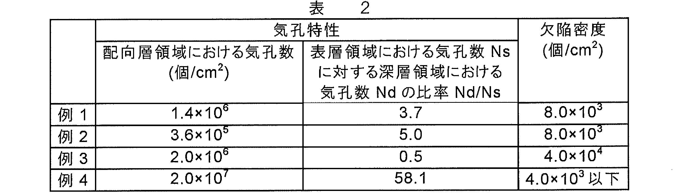
Claims (16)
- 13族元素の窒化物又は酸化物の結晶成長のために用いられる配向層を備えた下地基板であって、
前記配向層の前記結晶成長に用いられる側の表面が、サファイアよりも大きいa軸長及び/又はc軸長を有するコランダム型結晶構造を有する材料で構成されており、かつ、
前記配向層中に複数の気孔が存在する、下地基板。 - 前記配向層において、前記表面を含む表層領域における気孔数が、前記表面から離れた深層領域における気孔数よりも低減されている、請求項1に記載の下地基板。
- 前記配向層の前記a軸長及び/又はc軸長が、前記配向層の表面と裏面で異なる、請求項1又は2に記載の下地基板。
- 前記配向層の全体が前記コランダム型結晶構造を有する材料で構成される、請求項1~3のいずれか一項に記載の下地基板。
- 前記コランダム型結晶構造を有する材料が、α-Cr2O3、α-Fe2O3、α-Ti2O3、α-V2O3、α-Ga2O3、α-In2O3及びα-Rh2O3からなる群から選択される材料、又はα-Al2O3、α-Cr2O3、α-Fe2O3、α-Ti2O3、α-V2O3、α-Ga2O3、α-In2O3及びα-Rh2O3からなる群から選択される2種以上を含む固溶体を含む、請求項1~4のいずれか一項に記載の下地基板。
- 前記コランダム型結晶構造を有する材料が、α-Cr2O3を含む材料、又はα-Cr2O3と異種材料との固溶体を含む材料である、請求項1~5のいずれか一項に記載の下地基板。
- 前記コランダム型結晶構造を有する材料が、α-Cr2O3、α-Fe2O3及びα-Ti2O3からなる群から選ばれる1種以上の材料若しくはそれらの固溶体、又はα-Al2O3と、α-Cr2O3、α-Fe2O3及びα-Ti2O3からなる群から選ばれる1種以上の材料とを含む固溶体を含む、請求項1~5のいずれか一項に記載の下地基板。
- 前記表面における前記コランダム型結晶構造を有する材料のa軸長が4.754Åより大きく5.487Å以下である、請求項1~7のいずれか一項に記載の下地基板。
- 前記配向層内に、厚さ方向に組成が変化する傾斜組成領域が存在する、請求項1~8のいずれか一項に記載の下地基板。
- 前記傾斜組成領域の厚さが20μm以上である、請求項9に記載の下地基板。
- 前記配向層が、前記表面近くに位置する、厚さ方向に組成が安定している組成安定領域と、前記表面から遠くに位置する、厚さ方向に組成が変化する傾斜組成領域とを有する、請求項1~10のいずれか一項に記載の下地基板。
- 前記傾斜組成領域がα-Cr2O3とα-Al2O3とを含む固溶体で構成される、請求項9~11のいずれか一項に記載の下地基板。
- 前記傾斜組成領域においてAl濃度が前記組成安定領域に向かって厚さ方向に低下する、請求項9~12のいずれか一項に記載の下地基板。
- 前記配向層がヘテロエピタキシャル成長層である、請求項1~13のいずれか一項に記載の下地基板。
- 前記配向層の前記表面と反対側に支持基板をさらに備えた、請求項1~14のいずれか一項に記載の下地基板。
- 前記支持基板がサファイア基板である、請求項15に記載の下地基板。
Priority Applications (3)
| Application Number | Priority Date | Filing Date | Title |
|---|---|---|---|
| CN202080006855.9A CN113614293B (zh) | 2019-03-28 | 2020-02-18 | 基底基板 |
| JP2021508263A JP7124207B2 (ja) | 2019-03-28 | 2020-02-18 | 下地基板 |
| US17/443,828 US12421621B2 (en) | 2019-03-28 | 2021-07-28 | Underlying substrate |
Applications Claiming Priority (2)
| Application Number | Priority Date | Filing Date | Title |
|---|---|---|---|
| JP2019-063602 | 2019-03-28 | ||
| JP2019063602 | 2019-03-28 |
Related Child Applications (1)
| Application Number | Title | Priority Date | Filing Date |
|---|---|---|---|
| US17/443,828 Continuation US12421621B2 (en) | 2019-03-28 | 2021-07-28 | Underlying substrate |
Publications (1)
| Publication Number | Publication Date |
|---|---|
| WO2020195355A1 true WO2020195355A1 (ja) | 2020-10-01 |
Family
ID=72611798
Family Applications (1)
| Application Number | Title | Priority Date | Filing Date |
|---|---|---|---|
| PCT/JP2020/006312 Ceased WO2020195355A1 (ja) | 2019-03-28 | 2020-02-18 | 下地基板 |
Country Status (4)
| Country | Link |
|---|---|
| US (1) | US12421621B2 (ja) |
| JP (1) | JP7124207B2 (ja) |
| CN (1) | CN113614293B (ja) |
| WO (1) | WO2020195355A1 (ja) |
Cited By (1)
| Publication number | Priority date | Publication date | Assignee | Title |
|---|---|---|---|---|
| JPWO2024195374A1 (ja) * | 2023-03-23 | 2024-09-26 |
Families Citing this family (2)
| Publication number | Priority date | Publication date | Assignee | Title |
|---|---|---|---|---|
| CN113574215B (zh) * | 2019-03-28 | 2024-08-02 | 日本碍子株式会社 | 基底基板及其制造方法 |
| CN115652430B (zh) * | 2022-10-26 | 2025-12-30 | 杭州电子科技大学 | 一种层状Cr2O3晶体材料的制备方法 |
Citations (3)
| Publication number | Priority date | Publication date | Assignee | Title |
|---|---|---|---|---|
| JP2000106348A (ja) * | 1998-07-28 | 2000-04-11 | Matsushita Electronics Industry Corp | 化合物半導体層含有基板およびその製造方法ならびにこれを用いた半導体装置 |
| JP2014072533A (ja) * | 2013-10-10 | 2014-04-21 | Roca Kk | 半導体装置 |
| JP2016100593A (ja) * | 2014-11-26 | 2016-05-30 | 株式会社Flosfia | 結晶性積層構造体 |
Family Cites Families (12)
| Publication number | Priority date | Publication date | Assignee | Title |
|---|---|---|---|---|
| US6107213A (en) * | 1996-02-01 | 2000-08-22 | Sony Corporation | Method for making thin film semiconductor |
| US6344375B1 (en) * | 1998-07-28 | 2002-02-05 | Matsushita Electric Industrial Co., Ltd | Substrate containing compound semiconductor, method for manufacturing the same and semiconductor device using the same |
| EP0996145A3 (en) * | 1998-09-04 | 2000-11-08 | Canon Kabushiki Kaisha | Process for producing semiconductor substrate |
| JP4178936B2 (ja) * | 2002-12-11 | 2008-11-12 | 日本電気株式会社 | Iii族窒化物自立基板およびそれを用いた半導体素子ならびにそれらの製造方法 |
| JP2006282500A (ja) * | 2003-06-30 | 2006-10-19 | Kenichiro Miyahara | 薄膜形成用基板、薄膜基板、及び発光素子 |
| JP2005340379A (ja) * | 2004-05-25 | 2005-12-08 | Toshiba Ceramics Co Ltd | 化合物半導体及びその製造方法 |
| JP5955226B2 (ja) * | 2010-12-29 | 2016-07-20 | シャープ株式会社 | 窒化物半導体構造、窒化物半導体発光素子、窒化物半導体トランジスタ素子、窒化物半導体構造の製造方法および窒化物半導体素子の製造方法 |
| JP5343224B1 (ja) * | 2012-09-28 | 2013-11-13 | Roca株式会社 | 半導体装置および結晶 |
| JP5397795B1 (ja) * | 2013-06-21 | 2014-01-22 | Roca株式会社 | 半導体装置及びその製造方法、結晶及びその製造方法 |
| JP6349592B2 (ja) | 2014-07-22 | 2018-07-04 | 株式会社Flosfia | 半導体装置 |
| CN107068773B (zh) * | 2015-12-18 | 2021-06-01 | 株式会社Flosfia | 半导体装置 |
| CN106960781A (zh) * | 2017-03-28 | 2017-07-18 | 刘志斌 | 一种氮化镓薄膜及其制备方法和石墨烯薄膜及其制备方法 |
-
2020
- 2020-02-18 JP JP2021508263A patent/JP7124207B2/ja active Active
- 2020-02-18 CN CN202080006855.9A patent/CN113614293B/zh active Active
- 2020-02-18 WO PCT/JP2020/006312 patent/WO2020195355A1/ja not_active Ceased
-
2021
- 2021-07-28 US US17/443,828 patent/US12421621B2/en active Active
Patent Citations (3)
| Publication number | Priority date | Publication date | Assignee | Title |
|---|---|---|---|---|
| JP2000106348A (ja) * | 1998-07-28 | 2000-04-11 | Matsushita Electronics Industry Corp | 化合物半導体層含有基板およびその製造方法ならびにこれを用いた半導体装置 |
| JP2014072533A (ja) * | 2013-10-10 | 2014-04-21 | Roca Kk | 半導体装置 |
| JP2016100593A (ja) * | 2014-11-26 | 2016-05-30 | 株式会社Flosfia | 結晶性積層構造体 |
Non-Patent Citations (1)
| Title |
|---|
| HAI-SHENG QIAN, POERNOMO GUNAWAN, YUN-XIA ZHANG,GUO-FENG LIN, JIAN-WEI ZHENG, RONG XU: "Template-Free Synthesis of Highly Uniform α-GaOOH Spindles and Conversion to α-Ga 2 O 3 and β-Ga2O3", CRYSTAL GROWTH & DESIGN, vol. 8, no. 4, 28 February 2008 (2008-02-28), pages 1282 - 1287, XP055743532, ISSN: 1528-7483, DOI: 10.1021/cg701004w * |
Cited By (2)
| Publication number | Priority date | Publication date | Assignee | Title |
|---|---|---|---|---|
| JPWO2024195374A1 (ja) * | 2023-03-23 | 2024-09-26 | ||
| WO2024195374A1 (ja) * | 2023-03-23 | 2024-09-26 | 日本碍子株式会社 | 下地基板 |
Also Published As
| Publication number | Publication date |
|---|---|
| US20210355602A1 (en) | 2021-11-18 |
| US12421621B2 (en) | 2025-09-23 |
| JPWO2020195355A1 (ja) | 2021-10-14 |
| CN113614293A (zh) | 2021-11-05 |
| JP7124207B2 (ja) | 2022-08-23 |
| CN113614293B (zh) | 2024-08-02 |
Similar Documents
| Publication | Publication Date | Title |
|---|---|---|
| US12351941B2 (en) | Ground substrate and method for producing same | |
| JP6784871B1 (ja) | 半導体膜 | |
| JP7289357B2 (ja) | 半導体膜 | |
| US11942520B2 (en) | Semiconductor film | |
| US12421621B2 (en) | Underlying substrate | |
| JP7439117B2 (ja) | 下地基板及びその製造方法 | |
| WO2020194763A1 (ja) | 半導体膜 | |
| JP7320070B2 (ja) | 下地基板及びその製造方法 | |
| WO2020261574A1 (ja) | 半導体膜 | |
| WO2020261356A1 (ja) | 半導体膜 | |
| WO2020195497A1 (ja) | 半導体膜 |
Legal Events
| Date | Code | Title | Description |
|---|---|---|---|
| 121 | Ep: the epo has been informed by wipo that ep was designated in this application |
Ref document number: 20777576 Country of ref document: EP Kind code of ref document: A1 |
|
| ENP | Entry into the national phase |
Ref document number: 2021508263 Country of ref document: JP Kind code of ref document: A |
|
| NENP | Non-entry into the national phase |
Ref country code: DE |
|
| 122 | Ep: pct application non-entry in european phase |
Ref document number: 20777576 Country of ref document: EP Kind code of ref document: A1 |