WO2020194971A1 - ワークの両面研磨方法及びワークの両面研磨装置 - Google Patents
ワークの両面研磨方法及びワークの両面研磨装置 Download PDFInfo
- Publication number
- WO2020194971A1 WO2020194971A1 PCT/JP2019/051215 JP2019051215W WO2020194971A1 WO 2020194971 A1 WO2020194971 A1 WO 2020194971A1 JP 2019051215 W JP2019051215 W JP 2019051215W WO 2020194971 A1 WO2020194971 A1 WO 2020194971A1
- Authority
- WO
- WIPO (PCT)
- Prior art keywords
- work
- double
- polishing
- index
- wafer
- Prior art date
- Legal status (The legal status is an assumption and is not a legal conclusion. Google has not performed a legal analysis and makes no representation as to the accuracy of the status listed.)
- Ceased
Links
Images



Classifications
-
- B—PERFORMING OPERATIONS; TRANSPORTING
- B24—GRINDING; POLISHING
- B24B—MACHINES, DEVICES, OR PROCESSES FOR GRINDING OR POLISHING; DRESSING OR CONDITIONING OF ABRADING SURFACES; FEEDING OF GRINDING, POLISHING, OR LAPPING AGENTS
- B24B37/00—Lapping machines or devices; Accessories
- B24B37/005—Control means for lapping machines or devices
-
- B—PERFORMING OPERATIONS; TRANSPORTING
- B24—GRINDING; POLISHING
- B24B—MACHINES, DEVICES, OR PROCESSES FOR GRINDING OR POLISHING; DRESSING OR CONDITIONING OF ABRADING SURFACES; FEEDING OF GRINDING, POLISHING, OR LAPPING AGENTS
- B24B37/00—Lapping machines or devices; Accessories
- B24B37/04—Lapping machines or devices; Accessories designed for working plane surfaces
- B24B37/07—Lapping machines or devices; Accessories designed for working plane surfaces characterised by the movement of the work or lapping tool
- B24B37/08—Lapping machines or devices; Accessories designed for working plane surfaces characterised by the movement of the work or lapping tool for double side lapping
-
- B—PERFORMING OPERATIONS; TRANSPORTING
- B24—GRINDING; POLISHING
- B24B—MACHINES, DEVICES, OR PROCESSES FOR GRINDING OR POLISHING; DRESSING OR CONDITIONING OF ABRADING SURFACES; FEEDING OF GRINDING, POLISHING, OR LAPPING AGENTS
- B24B37/00—Lapping machines or devices; Accessories
- B24B37/11—Lapping tools
- B24B37/12—Lapping plates for working plane surfaces
-
- B—PERFORMING OPERATIONS; TRANSPORTING
- B24—GRINDING; POLISHING
- B24B—MACHINES, DEVICES, OR PROCESSES FOR GRINDING OR POLISHING; DRESSING OR CONDITIONING OF ABRADING SURFACES; FEEDING OF GRINDING, POLISHING, OR LAPPING AGENTS
- B24B37/00—Lapping machines or devices; Accessories
- B24B37/34—Accessories
-
- B—PERFORMING OPERATIONS; TRANSPORTING
- B24—GRINDING; POLISHING
- B24B—MACHINES, DEVICES, OR PROCESSES FOR GRINDING OR POLISHING; DRESSING OR CONDITIONING OF ABRADING SURFACES; FEEDING OF GRINDING, POLISHING, OR LAPPING AGENTS
- B24B49/00—Measuring or gauging equipment for controlling the feed movement of the grinding tool or work; Arrangements of indicating or measuring equipment, e.g. for indicating the start of the grinding operation
- B24B49/02—Measuring or gauging equipment for controlling the feed movement of the grinding tool or work; Arrangements of indicating or measuring equipment, e.g. for indicating the start of the grinding operation according to the instantaneous size and required size of the workpiece acted upon, the measuring or gauging being continuous or intermittent
- B24B49/03—Measuring or gauging equipment for controlling the feed movement of the grinding tool or work; Arrangements of indicating or measuring equipment, e.g. for indicating the start of the grinding operation according to the instantaneous size and required size of the workpiece acted upon, the measuring or gauging being continuous or intermittent according to the final size of the previously ground workpiece
-
- H—ELECTRICITY
- H10—SEMICONDUCTOR DEVICES; ELECTRIC SOLID-STATE DEVICES NOT OTHERWISE PROVIDED FOR
- H10P—GENERIC PROCESSES OR APPARATUS FOR THE MANUFACTURE OR TREATMENT OF DEVICES COVERED BY CLASS H10
- H10P52/00—Grinding, lapping or polishing of wafers, substrates or parts of devices
-
- H—ELECTRICITY
- H10—SEMICONDUCTOR DEVICES; ELECTRIC SOLID-STATE DEVICES NOT OTHERWISE PROVIDED FOR
- H10P—GENERIC PROCESSES OR APPARATUS FOR THE MANUFACTURE OR TREATMENT OF DEVICES COVERED BY CLASS H10
- H10P72/00—Handling or holding of wafers, substrates or devices during manufacture or treatment thereof
- H10P72/04—Apparatus for manufacture or treatment
- H10P72/0428—Apparatus for mechanical treatment or grinding or cutting
Definitions
- the present invention relates to a double-sided polishing method for a work and a double-sided polishing device for a work.
- Patent Document 1 proposes a method of controlling the amount of polishing of a work.
- the GBIR value may vary between batches, so it was desired to suppress it.
- An object of the present invention is to provide a double-sided polishing method for a work and a double-sided polishing device for a work, which can suppress variations in GBIR values of the work after polishing between batches.
- the gist structure of the present invention is as follows.
- the double-sided polishing method for the workpiece of the present invention After double-sided polishing in the previous batch, the measuring unit measures the thickness of the work at each of the plurality of measurement points in the plane of the work that has been double-sided polished, and the first calculation unit measures the plurality of measurement points.
- a pre-polishing index calculation step for calculating an index Xp obtained by integrating the thickness of the work measured at each measurement point in the plane of the work.
- a target polishing time calculation step for calculating the target polishing time Tt in the current batch using the prediction formula is characterized by including a double-sided polishing step in which the control unit controls the work to be double-sided polished using the target polishing time Tt calculated in the target polishing time calculation step, and performs the double-sided polishing.
- “measuring the thickness of the work” means not only directly measuring the thickness of the work but also measuring a parameter correlating with the thickness of the work and using the parameter to measure the thickness of the work. Is also included in the calculation.
- the “GBIR value” means the GBIR defined in the SEMI standard M1 and the SEMI standard MF1530.
- the index Xp is the sum of the thickness of the work measured at each of the measurement points for one of the two coordinate axes in the plane of the work, and further for the other coordinate axis. It is preferable to calculate by integrating.
- the two coordinate axes are composed of a coordinate axis in the radial direction of the work and a coordinate axis in the circumferential direction of the work.
- the index Xp is preferably obtained by integrating the thickness of the work measured at each of the measurement points in the circumferential direction of the work and further integrating in the radial direction of the work.
- the index Xp is The in-plane of the work is divided into a plurality of micro-planes including one or more of the measurement points.
- the thickness of the work on the minute surface was calculated based on the thickness of the work measured at each of the measurement points included in the minute surface. It is preferable that the calculated thickness of the work on the minute surface is calculated by integrating the thickness of the work in the surface of the work.
- the thickness of the work on the micro surface is preferably an average value of the thickness of the work measured at each of the measurement points for partitioning the micro surface.
- the measurement points are preferably located at equal intervals on at least one of the two coordinate axes in the plane of the work.
- A1, A2, A3, A4, ⁇ , ⁇ , and ⁇ is a coefficient obtained by regression analysis or a predetermined coefficient given in advance.
- A1, A2, A3, A4, ⁇ , ⁇ , and ⁇ at least one or more is preferably a coefficient obtained by regression analysis.
- the double-sided polishing step is performed.
- a rotary surface plate having an upper surface plate and a lower surface plate, a sun gear provided at the center of the rotary surface plate, an internal gear provided at an outer peripheral portion of the rotary surface plate, the upper surface plate and the lower surface plate.
- a batch provided with a carrier plate provided between the two and having one or more holding holes for holding the work, and polishing pads are attached to the lower surface of the upper surface plate and the upper surface of the lower surface plate, respectively. It is preferable to use a double-sided polishing device for the work of the processing method.
- the double-sided polishing step is performed.
- a step of relatively rotating the rotary surface plate and the carrier plate while supplying the polishing slurry onto the polishing pad and polishing both sides of the work using the calculated polishing time of the current batch may be included. preferable.
- the work is preferably a wafer.
- the double-sided polishing device for the workpiece of the present invention A rotary surface plate having an upper surface plate and a lower surface plate, a sun gear provided at the center of the rotary surface plate, an internal gear provided at an outer peripheral portion of the rotary surface plate, the upper surface plate and the lower surface plate.
- a carrier plate provided between the two and having one or more holding holes for holding the work is provided, and polishing pads are attached to the lower surface of the upper surface plate and the upper surface of the lower surface plate, respectively.
- a measuring unit that measures the thickness of the work that has undergone double-sided polishing
- the first calculation unit which calculates the index Xp by integrating the measured thickness of the work in the plane of the work
- the target polishing time Tt in the current batch is calculated using a predetermined prediction formula which is a relational expression between the target polishing time Tt in the current batch, the index Xp, and the index Xt set as the target in the previous batch.
- the second calculation part and It is characterized by further including a control unit that controls the work to be polished on both sides by using the calculated target polishing time Tt.
- the double-sided polishing method for wafers of the present invention it is possible to provide a double-sided polishing method for a workpiece and a double-sided polishing apparatus for a workpiece, which can suppress variations in GBIR values of the workpiece after polishing between batches.
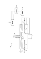
- FIG. 1 is a front view schematically showing a double-sided polishing apparatus for a work according to an embodiment of the present invention.
- the double-sided polishing apparatus 100 includes a rotary surface plate 6 having an upper surface plate 2 and a lower surface plate 4, a sun gear 8 provided at the center of the rotary surface plate 6, and an outer circumference of the rotary surface plate 6.
- a carrier plate 12 provided between an internal gear 10 provided in a portion and between an upper surface plate 2 and a lower surface plate 4 and having one or more holding holes (not shown) for holding a work (wafer in this example).
- holding holes not shown
- polishing pads are attached to the lower surface of the upper surface plate 2 and the upper surface of the lower surface plate 4, respectively. Further, the double-sided polishing apparatus 100 is provided with a slurry supply mechanism 14 for supplying a polishing slurry at the center of the upper surface plate 2.
- the double-sided polishing apparatus 100 further includes a control unit 16, a measurement unit 18, and a storage unit 20.
- the control unit 16 integrates the measured wafer thickness with the control unit (controller) that controls the rotation of the upper surface plate 2, the lower surface plate 4, the sun gear 8, and the internal gear 10 and indexes it.
- the first calculation unit (first calculator) for calculating Xp (details will be described later), the target polishing time Tt in the current batch, the index Xp, and the index Xt set as the target in the previous batch.
- the target polishing time Tt in the current batch is calculated (details will be described later), the second calculation unit (second calculator), and the batch processing are terminated. It has a determination unit (processor) for determining whether or not it is present.
- the first calculation unit and the second calculation unit may be configured as separate units or the same unit.
- the control unit is also configured to be able to control the wafer to be polished on both sides by using the calculated target polishing time Tt.
- the control unit 16 can be realized by a central processing unit (CPU) inside the computer.
- the measuring unit 18 is not particularly limited, but can be realized by using, for example, a spectroscopic interference displacement device.
- the wafer at each measurement point is compared with the wafer obtained by performing double-side polishing in the previous batch. Measure the thickness of.
- the storage unit 20 stores the target polishing time, the measured value of the wafer thickness, and the indexes Xp and Xt described later.
- the storage unit 20 can be any known memory, and can be realized by using, for example, a hard disk, a ROM, or a RAM.
- FIG. 2 is a flowchart showing a method of double-sided polishing of a work according to an embodiment of the present invention.
- the double-sided polishing method for the work according to the embodiment of the present invention shown in FIG. 2 can be performed using, for example, the double-sided polishing device for the work according to the embodiment of the present invention shown in FIG.
- a double-sided polishing method for a work according to an embodiment of the present invention will be described with reference to FIGS. 1 and 2.
- a wafer (silicon wafer in this example) is used as the work (hereinafter, described as a wafer).
- the measuring unit 18 sets a plurality of measuring points in the plane of the wafer (step S101).
- two coordinate axes are taken in the plane of the wafer, and in this example, the two coordinate axes consist of a coordinate axis in the radial direction of the wafer and a coordinate axis in the circumferential direction of the wafer.
- a plurality of measurement points having different radial distances from the center of the wafer in the plane of the wafer are set, and further, the radial distances from the center of the wafer in the plane of the wafer are the same.
- a plurality of measurement points are set in the circumferential direction of the wafer. It is preferable that the in-plane measurement points of the wafer are set so as to be uniformly located in the in-plane of the wafer.
- the setting of the measurement points in the present embodiment will be described more specifically.
- the measurement points are set at 1 mm intervals at equal intervals in the radial direction from the center of the wafer.
- the center of the wafer is also set as the measurement point.
- the above interval does not have to be 1 mm, and can be set in various ways according to the diameter of the wafer and the like.
- the measurement points are preferably set so as to be located at equal intervals in the radial direction as in this example, but they can also be set at non-equal intervals.
- measurement points are set at equal intervals of 1 ° in the circumferential direction of the wafer on the entire circumference of the wafer.
- the above interval does not have to be 1 ° and can be set in various ways.
- the thickness of the wafer is measured at each of a plurality of measurement points in the plane of the wafer subjected to double-side polishing (step).
- step 101 Part of the pre-polishing index calculation process).
- the thickness of the wafer is measured at all the measurement points of the above 106561 measurement points.
- the measuring unit 18 can measure the thickness of the wafer at all the above measurement points after double-sided polishing in the previous batch. It can.
- the spectral interference displacement device is provided so as to face the first sensor unit (not shown) for measuring the front surface of the wafer and the first sensor unit, and measures the back surface of the wafer. It has a second sensor unit (not shown) and a calculation unit (not shown), and performs the following measurements. The first sensor unit and the second sensor unit irradiate each measurement point on the front and back surfaces of the wafer with light in a wide wavelength band and receive the reflected light reflected at the center.
- the calculation unit analyzes the reflected light received by each sensor unit to calculate the thickness of the wafer at each measurement point.
- the measured wafer thickness is transmitted to the control unit 16 and stored in the storage unit 20.
- the thickness of the wafer can be measured by using various other measuring devices, or a parameter correlating with the thickness of the wafer is measured and the thickness of the wafer is calculated from the parameter. You can also do it.
- the first calculation unit calculates an index Xp obtained by integrating the thicknesses of the wafers measured at each of the plurality of measurement points (the following steps). S103 to step S105). Specifically, the index Xp can be calculated as follows.
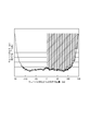
- FIG. 3 shows the radial position of the measurement point from the center of the wafer when the thickness of the wafer measured at each measurement point was averaged in the circumferential direction of the wafer, and the thickness was averaged in the circumferential direction. It is a figure which shows the relationship with the thickness of a wafer.
- FIG. 3 on the horizontal axis, one side in the radial direction of the wafer is shown as plus and the other side is shown as minus. As shown in FIGS.
- the thickness of the wafer measured at each of a plurality of measurement points having the same radial distance from the center of the wafer is integrated in the circumferential direction of the wafer ( In this example, averaging) (step S103: part of the pre-polishing index calculation step).
- averaging step S103: part of the pre-polishing index calculation step.
- the difference between the thickness averaged in the circumferential direction of the wafer and the predetermined reference thickness is calculated (step S104: a part of the pre-polishing index calculation step).
- the predetermined reference thickness is the entire circumferential direction of the radial region from the position of 2 mm inward in the radial direction of the wafer from the outer peripheral edge of the wafer to the position of 10 mm inward in the radial direction of the wafer from the outer peripheral edge of the wafer. It is the average thickness at the measurement point inside.
- the predetermined reference thickness can be an average value, a maximum value, or a minimum value of the thickness of the wafer in other regions, or can be arbitrarily set as appropriate.
- the thickness averaged in the circumferential direction of the wafer can be used as it is (step S104 is omitted) without calculating the difference using a predetermined reference thickness.
- the step S104 is followed by the step S103, but the step S104 is not limited to this case. The difference is calculated first, and then the difference is integrated in the circumferential direction of the wafer (average). It may be calculated at the same time.
- the index Xp obtained by further integrating the above differences in the radial direction of the wafer is calculated (step S105: a part of the pre-polishing index calculation step). Specifically, as shown in FIG. 3, the index Xp obtained by integrating the difference calculated in step S105 in the radial direction of the wafer is calculated.
- the interval between the horizontal axes is set to 12.5 mm only on one side (plus side) in the radial direction of the wafer, and the product is the product of the thickness of the wafer averaged in the circumferential direction of the vertical axis. Shows a rectangle.
- the index Xp can be calculated as the sum of the rectangular areas including the horizontal axis of 1 mm and the vertical axis of the wafer thickness.
- the index Xp is calculated by integrating (averaging) the thickness of the wafer measured at each measurement point in the circumferential direction of the wafer and further integrating it in the radial direction of the wafer. It is also possible to calculate by integrating (averaging) the thickness of the wafer measured in each in the radial direction of the wafer and further integrating in the circumferential direction of the wafer. Further, for the above index Xp, an average value obtained by dividing by the number of measurement points or the like can be further calculated, and the average value can be used as the index Xp.
- a coordinate axis in the radial direction of the wafer and a coordinate axis in the circumferential direction of the wafer are taken, and the index Xp is the wafer measured at each measurement point.
- the thickness of the wafer is integrated in the circumferential direction of the wafer and further integrated in the radial direction of the wafer to obtain the thickness.
- the in-plane Cartesian coordinates of the wafer (for example, orthogonal to the x-axis and the x-axis) are obtained.
- the y-axis) is taken, and the index Xp is obtained by integrating (including averaging) the thickness of the wafer measured at each measurement point on the x-axis and integrating (including averaging) on the y-axis, or y. It is also possible to calculate by integrating (including averaging) on the x-axis and integrating (including averaging) on the axis.
- the measurement points can be set at equal intervals of 1 mm on the x-axis and the y-axis.
- the above interval does not have to be 1 mm and can be set in various ways according to the diameter of the wafer and the like.
- the measurement points are preferably set so as to be located at equal intervals on the x-axis and / or the y-axis, but the measurement points should be set at non-equal intervals on either or both of the x-axis and the y-axis. You can also.
- the difference can be calculated using a predetermined reference thickness, or may not be used.
- the index Xp can be obtained by further calculating an average value divided by the number of measurement points or the like, and using the average value as the index Xp.
- step S106 the determination unit of the control unit 16 determines whether or not to end the batch processing. For this determination, for example, the calculated index Xp and a predetermined threshold value of the index can be used. If the first batch is not double-sided polished, the batch process is not normally completed, so step S106 can be skipped and the process can proceed to step S107 described later. However, even when the first batch of double-sided polishing is not performed, the determination in step S106 can be performed, and the determination result can be used to proceed to step S107 described later.
- the target polishing time Tt in the current batch and the pre-polishing index calculation are performed by the second calculation unit.
- the target polishing time Tt in the current batch is calculated by using a predetermined prediction formula which is a relational expression between the index Xp calculated in the process and the index Xt targeted in the previous batch (step S107: target polishing time). Calculation process).
- the predetermined prediction formula can be expressed by, for example, the following (Equation 1).
- each of A1, A2, A3, A4, ⁇ , ⁇ , and ⁇ is a coefficient obtained by regression analysis or a predetermined coefficient given in advance.
- At least one or more of A1, A2, A3, A4, ⁇ , ⁇ , and ⁇ are coefficients obtained by regression analysis.
- the prediction formula is not limited to the above example, and various formulas can be used.
- Equation 2 can be used for brevity.
- each of B1, B2, and B3 is a coefficient obtained by regression analysis or a predetermined coefficient given in advance.
- At least one or more of B1, B2, and B3 are coefficients obtained by regression analysis.
- an index Xt within a predetermined range (for example, a range required from the specifications) can be set based on past results and the like. From the second batch onward, the index targeted in the previous batch may be used.
- predetermined coefficients given in advance can be appropriately determined by using, for example, actual results in past batch processing.
- the coefficients obtained by the regression analysis are appropriately determined from the past results in the first batch, and the above prediction formulas (for example, (Equation 1) and (for example) It can be determined by regression analysis using Eq. 2)).
- the target polishing time in the current batch is used by using the above prediction formulas (for example, (Equation 1) and (Equation 2)). Tt can be calculated.
- the control unit 16 controls the wafer to be double-sided polished using the target polishing time Tt calculated in the target polishing time calculation step (step S107), and performs the double-sided polishing.
- Step S108 double-sided polishing step. Specifically, when the target polishing time Tt is calculated, the control unit 16 rotates the upper surface plate 2, the lower surface plate 4, the sun gear 8, and the internal gear 10. As a result, double-sided polishing of the wafer is started. Then, in double-sided polishing, the wafer is held on a carrier plate 12 provided with one or more holding holes for holding the wafer, the wafer is sandwiched between the rotary surface plates 6 composed of the upper surface plate 2 and the lower surface plate 4, and the slurry is supplied.
- the polishing time for double-sided polishing may be the calculated target polishing time Tt itself, or the calculated target polishing time Tt may be corrected (for example, a correction coefficient is added or multiplied). May be.
- step S106 the above steps are repeated until the determination unit of the control unit 16 determines that the batch processing is to be completed, and when it is determined that the batch processing is to be completed, the batch processing is terminated (step S109).
- FIG. 4 is a flowchart showing a double-sided polishing method for a work according to another embodiment of the present invention.
- a plurality of in-plane measurement points of the wafer are set (step S201), and after double-side polishing in the previous batch, a plurality of in-plane polishing of the wafer is performed.
- the thickness of the wafer is measured at each of the measurement points of (Step S202: Part of the pre-polishing index calculation step).
- the details of steps S201 and S202 are the same as those of steps S101 and S102 in the embodiment shown in FIG. 2, and thus the description thereof will be omitted.
- the index Xp is calculated as follows.
- the in-plane of the wafer is divided into a plurality of microplanes including one or more measurement points, and each of the plurality of microplanes is at each of the measurement points included in the microplanes.
- the wafer thickness on the minute surface is calculated (steps S203 to S206 below). The calculation can be performed by the first calculation unit.
- a predetermined reference plane is calculated using the measured wafer thickness (step S203: a part of the pre-polishing index calculation step).
- FIG. 5 is a diagram for explaining a method of calculating the reference plane.
- each measurement point in the circumferential direction of the wafer (in this example, the measurement points are set at equal intervals of 1 ° in the circumferential direction, so that each measurement point in the 360 direction is set.
- the maximum value of the wafer thickness in the radial region where the absolute value of the radial distance from the center of the wafer is 140 to 148 mm is adopted, and the maximum thickness of 360 wafers is used, and the minimum value is two.
- a reference plane having the minimum error is calculated as a plane consisting of the 360 points.
- FIG. 5 for the sake of simplicity, a plot of only 21 points in the circumferential direction is shown, but in this example, the maximum value of 360 points in the circumferential direction is used.
- FIG. 6 is a diagram for explaining a method of calculating the thickness of the wafer on the minute surface.
- the in-plane of the wafer is divided into a plurality of minute surfaces including one or more measurement points (step S204: one of the pre-polishing index calculation steps). Department).
- the measurement points are set at equal intervals of 1 mm in the radial direction of the wafer and at equal intervals of 1 ° in the circumferential direction of the wafer (shown in FIG. 2). Similar to the embodiment).
- FIG. 2 Similar to the embodiment.
- step S205 a part of the pre-polishing index calculation step.
- the thickness of the wafer on the micro surface is calculated based on the thickness of the wafer measured at each of the measurement points included in the micro surface (step S206: before polishing). Part of the index calculation process).
- each microfacet contains four measurement points (three if the center of the wafer is included).
- the average value of the thickness of the wafer measured at each of the four measurement points (three when the center of the wafer is included) when the reference plane calculated in step S203 is used as a reference is set to the wafer on the minute surface. It can be calculated and used as the thickness of.
- the calculated thickness of the wafer on the minute surface is integrated on the surface in the surface of the wafer to calculate the index Xp (steps S207 and S208 below). ). Specifically, first, the product of the area of the minute surface calculated in step S205 and the thickness of the wafer on the minute surface calculated in step S206 is calculated (step S207: a part of the pre-polishing index calculation step).
- step S208 a part of the pre-polishing index calculation step.
- the determination unit of the control unit 16 determines whether or not to end the batch processing (step S209).
- the target polishing time Tt in the current batch and the pre-polishing index calculation step are calculated by the second calculation unit.
- the target polishing time Tt in the current batch is calculated using a predetermined prediction formula which is a relational expression between the index Xp obtained and the index Xt targeted in the previous batch (step S210: target polishing time calculation step). ..
- step S210 the control unit 16 controls the wafer to be double-sided polished using the target polishing time Tt calculated in the target polishing time calculation step (step S210), and performs the double-sided polishing.
- Step S211 Double-sided polishing step.
- the process proceeds to the next batch, and for the polished wafer, the process returns to step S202, and steps S202 to S209 are repeated.
- step S209 the above steps are repeated until the determination unit of the control unit 16 determines that the batch processing is completed, and when it is determined that the batch processing is to be completed, the batch processing is terminated (step S211).
- the details of each of steps S209 to S212 are the same as those of steps S106 to S109 in the embodiment shown in FIG. 2, and thus the description thereof will be omitted.
- the above-mentioned reference plane determination method is only an example, and there are various other determination methods.
- the maximum value of the wafer thickness in the radial region where the absolute value of the radial distance from the center of the wafer is 140 to 148 mm is used, but the minimum value or the average value can also be used.
- the maximum value, the minimum value, and the average value in other regions can also be used.
- the reference plane does not necessarily have to be calculated, and step S203 may be omitted.
- the method of taking the minute surface is also various, and in the above example, the four measurement points most adjacent to each other in the circumferential direction and the radial direction of the wafer are included (the four points).
- a microplane (enclosed by measurement points) was used, but for example, a microplane surrounded by three measurement points forming a triangle in a plan view can be used, or a microplane surrounded by one measurement point can be used. It is also possible to partition into small microplanes (so that each microplane contains only one measurement point). Further, when the wafer is divided into minute surfaces, it is sufficient that the set of minute surfaces is uniformly arranged on 80% or more of the total area of the wafer, and it is not always necessary to divide the entire surface of the wafer.
- the thickness of the wafer on the minute surface is calculated by using the average value of four points, but it can also be calculated by using another method such as the maximum value and the minimum value.
- the thickness of the wafer measured at the measurement point can be used as it is as the thickness of the wafer on the minute surface.
- step S203 is performed before step S204 and step S205, but may be performed after or at the same time as step S204 and step S205.
- step S205 is performed before step S206, but may be performed after or at the same time as step S206.
- the double-sided polishing method for the work and the double-sided polishing device for the work according to the other embodiments of the present invention described above can also suppress variations in the GBIR value of the work after polishing between batches.
- examples of the present invention will be described, but the present invention is not limited to the following examples.
- each coefficient is set in advance, and the target index in (2) above is used as the index Xp, and the initial value of the index in (2) above is used as the index Xt.
- the target polishing time was calculated based on the prediction formula.
- the GBIR value was obtained from the calculated target polishing time as follows without performing double-sided polishing based on the calculated target polishing time. First, a proportional coefficient (“calculated index” / “target polishing time”) between the calculated index and the target polishing time is set in advance, and the proportional coefficient is set to the target polishing time calculated in (3). Multiplied.
- the four measurement points (three points when the center of the wafer is included) that are most adjacent to each other in the circumferential direction and the radial direction of the wafer are included (three points when the center of the wafer is included).
- the thickness of the wafer on the minute surface (enclosed by) is obtained as the average thickness based on the reference planes of the four points, and the thickness of the wafer on the minute surface is integrated in the plane of the wafer. It was used as an index (in Table 1, it is referred to as the "second index").
- GBIR was used as an index. Specifically, it is as follows. (1) First, a distribution of predicted values (target polishing time Tt) and polishing results (GBIR value after polishing) calculated using a prediction formula was created from the polishing results of 1000 wafers. (2) In the comparative example, GBIR was used as an index. Then, the initial values of the target GBIR and GBIR were set for the first batch processing. (3) In the above-mentioned prediction formula, each coefficient is set in advance, and the target GBIR in the above (2) is used as an index Xp, and the initial value of the GBIR in the above (2) is used as an index Xt in the next batch.
- the target polishing time was calculated based on the prediction formula.
- the GBIR value was obtained from the calculated target polishing time as follows without performing double-sided polishing based on the calculated target polishing time.
- a proportional coefficient (“calculated GBIR” / “target polishing time”) between the calculated GBIR and the target polishing time is set in advance, and the proportional coefficient is set to the target polishing time calculated in (3). Multiplied.
- the GBIR calculated from the calculated target polishing time was calculated back.
- the calculated index was searched from the distribution in (1), and the results associated with it were selected.
- the actual result (GBIR) was saved as the result of this time.
- FIG. 7 is a diagram showing the relationship between each index and GBIR.
- Double-sided polishing device 2: Upper surface plate, 4: Lower platen, 6: Rotating surface plate, 8: Sangia, 10: Internal gear, 12: Carrier plate, 14: Slurry supply mechanism, 16: Control unit, 18: Measuring unit, 20: Memory,
Landscapes
- Engineering & Computer Science (AREA)
- Mechanical Engineering (AREA)
- Mechanical Treatment Of Semiconductor (AREA)
- Finish Polishing, Edge Sharpening, And Grinding By Specific Grinding Devices (AREA)
- Constituent Portions Of Griding Lathes, Driving, Sensing And Control (AREA)
Abstract
本発明のワークの両面研磨方法は、前バッチでの両面研磨後に、該両面研磨を行ったワークに対して指標Xpを算出する、研磨前指標算出工程と、所定の予測式を用いて、前記現バッチでの目標研磨時間を算出する、目標研磨時間算出工程と、前記目標研磨時間を用いて、ワークを両面研磨する、両面研磨工程と、を含む。また、本発明のワークの両面研磨装置は、前バッチでの両面研磨後に、該両面研磨を行った前記ワークの厚さを測定する、測定部と、指標Xpを算出する、第1の計算部と、所定の予測式を用いて、前記現バッチでの目標研磨時間Ttを算出する、第2の計算部と、前記目標研磨時間Ttを用いて、前記ワークを両面研磨するように制御する、制御部と、を備える。
Description
本発明は、ワークの両面研磨方法及びワークの両面研磨装置に関するものである。
従来、シリコンウェーハ等のワークの平坦性を高めるために、研磨パッドを有する上下定盤でワークを挟み、その表裏面を同時に研磨する両面研磨が行われている。例えば、特許文献1では、ワークの研磨量を制御する手法が提案されている。
両面研磨においては、GBIR値がバッチ間でばらつくことがあるため、それを抑制することが望まれていた。
本発明は、研磨後のワークのGBIR値のバッチ間でのばらつきを抑制することができる、ワークの両面研磨方法及びワークの両面研磨装置を提供することを目的とする。
本発明の要旨構成は、以下の通りである。
本発明のワークの両面研磨方法は、
測定部により、前バッチでの両面研磨後に、該両面研磨を行ったワークの面内の複数の測定点の各々において、前記ワークの厚さを測定し、第1の計算部により、前記複数の測定点の各々において測定した前記ワークの厚さを、前記ワークの面内で積算して求められる指標Xpを算出する、研磨前指標算出工程と、
第2の計算部により、現バッチでの目標研磨時間Ttと、前記研磨前指標算出工程において算出された前記指標Xpと、前バッチで目標として設定した指標Xtとの関係式である、所定の予測式を用いて、前記現バッチでの目標研磨時間Ttを算出する、目標研磨時間算出工程と、
制御部により、前記目標研磨時間算出工程において算出された前記目標研磨時間Ttを用いて、ワークを両面研磨するように制御して、該両面研磨を行う、両面研磨工程と、を含むことを特徴とする。
なお、本明細書において、「ワークの厚さを測定」とは、ワークの厚さを直接測定することの他、ワークの厚さと相関のあるパラメータを測定して、該パラメータからワークの厚さを算出する場合も含むものとする。
また、「GBIR値」とは、SEMI規格 M1、及びSEMI規格 MF1530に規定されるGBIRを意味する。
本発明のワークの両面研磨方法は、
測定部により、前バッチでの両面研磨後に、該両面研磨を行ったワークの面内の複数の測定点の各々において、前記ワークの厚さを測定し、第1の計算部により、前記複数の測定点の各々において測定した前記ワークの厚さを、前記ワークの面内で積算して求められる指標Xpを算出する、研磨前指標算出工程と、
第2の計算部により、現バッチでの目標研磨時間Ttと、前記研磨前指標算出工程において算出された前記指標Xpと、前バッチで目標として設定した指標Xtとの関係式である、所定の予測式を用いて、前記現バッチでの目標研磨時間Ttを算出する、目標研磨時間算出工程と、
制御部により、前記目標研磨時間算出工程において算出された前記目標研磨時間Ttを用いて、ワークを両面研磨するように制御して、該両面研磨を行う、両面研磨工程と、を含むことを特徴とする。
なお、本明細書において、「ワークの厚さを測定」とは、ワークの厚さを直接測定することの他、ワークの厚さと相関のあるパラメータを測定して、該パラメータからワークの厚さを算出する場合も含むものとする。
また、「GBIR値」とは、SEMI規格 M1、及びSEMI規格 MF1530に規定されるGBIRを意味する。
上記においては、前記指標Xpは、前記測定点の各々において測定した前記ワークの厚さを、前記ワークの面内の2つの座標軸のうちの一方の座標軸について積算したものを、他方の座標軸についてさらに積算して求められることが好ましい。
上記においては、前記2つの座標軸は、前記ワークの径方向である座標軸と、前記ワークの周方向である座標軸とからなり、
前記指標Xpは、前記測定点の各々において測定した前記ワークの厚さを、前記ワークの周方向に積算したものを、前記ワークの径方向にさらに積算して求められることが好ましい。
前記指標Xpは、前記測定点の各々において測定した前記ワークの厚さを、前記ワークの周方向に積算したものを、前記ワークの径方向にさらに積算して求められることが好ましい。
本発明のワークの両面研磨方法においては、前記指標Xpは、
前記ワークの面内を、前記測定点の1つ以上を含む、複数の微小面に分割し、
前記複数の微小面の各々について、前記微小面に含まれる前記測定点の各々において計測した前記ワークの厚さに基づいて、前記微小面における前記ワークの厚さを算出し、
算出した前記微小面における前記ワークの厚さを、前記ワークの面内で、面で積算して算出されることが好ましい。
前記ワークの面内を、前記測定点の1つ以上を含む、複数の微小面に分割し、
前記複数の微小面の各々について、前記微小面に含まれる前記測定点の各々において計測した前記ワークの厚さに基づいて、前記微小面における前記ワークの厚さを算出し、
算出した前記微小面における前記ワークの厚さを、前記ワークの面内で、面で積算して算出されることが好ましい。
上記においては、前記微小面における前記ワークの厚さは、前記微小面を区画する測定点の各々において計測した前記ワークの厚さの平均値であることが好ましい。
本発明のワークの両面研磨方法においては、
前記測定点は、前記ワークの面内の2つの座標軸のうち、少なくとも一方の座標軸において、等間隔に位置することが好ましい。
前記測定点は、前記ワークの面内の2つの座標軸のうち、少なくとも一方の座標軸において、等間隔に位置することが好ましい。
本発明のワークの両面研磨方法においては、前記所定の予測式は、
A1×Ttα=A2×Xpβ+A3×Xtγ+A4
で表わされ、
A1、A2、A3、A4、α、β、γは、それぞれ、回帰分析で求められる係数であるか、あるいは、予め与えられた所定の係数であり、
A1、A2、A3、A4、α、β、γのうち、少なくとも1つ以上は、回帰分析で求められる係数であることが好ましい。
A1×Ttα=A2×Xpβ+A3×Xtγ+A4
で表わされ、
A1、A2、A3、A4、α、β、γは、それぞれ、回帰分析で求められる係数であるか、あるいは、予め与えられた所定の係数であり、
A1、A2、A3、A4、α、β、γのうち、少なくとも1つ以上は、回帰分析で求められる係数であることが好ましい。
本発明のワークの両面研磨方法においては、前記両面研磨工程は、
上定盤及び下定盤を有する回転定盤と、前記回転定盤の中心部に設けられたサンギアと、前記回転定盤の外周部に設けられたインターナルギアと、前記上定盤と前記下定盤との間に設けられ、前記ワークを保持する1つ以上の保持孔を有するキャリアプレートと、を備え、前記上定盤の下面及び前記下定盤の上面に研磨パッドがそれぞれ貼布された、バッチ処理方式の前記ワークの両面研磨装置を用いて行われることが好ましい。
上定盤及び下定盤を有する回転定盤と、前記回転定盤の中心部に設けられたサンギアと、前記回転定盤の外周部に設けられたインターナルギアと、前記上定盤と前記下定盤との間に設けられ、前記ワークを保持する1つ以上の保持孔を有するキャリアプレートと、を備え、前記上定盤の下面及び前記下定盤の上面に研磨パッドがそれぞれ貼布された、バッチ処理方式の前記ワークの両面研磨装置を用いて行われることが好ましい。
本発明のワークの両面研磨方法においては、前記両面研磨工程は、
前記研磨パッド上に研磨スラリーを供給しながら、前記回転定盤と前記キャリアプレートとを相対回転させて、算出した前記現バッチの研磨時間を用いて前記ワークの両面を研磨する工程を含むことが好ましい。
前記研磨パッド上に研磨スラリーを供給しながら、前記回転定盤と前記キャリアプレートとを相対回転させて、算出した前記現バッチの研磨時間を用いて前記ワークの両面を研磨する工程を含むことが好ましい。
本発明のワークの両面研磨方法においては、前記ワークは、ウェーハであることが好ましい。
本発明のワークの両面研磨装置は、
上定盤及び下定盤を有する回転定盤と、前記回転定盤の中心部に設けられたサンギアと、前記回転定盤の外周部に設けられたインターナルギアと、前記上定盤と前記下定盤との間に設けられ、ワークを保持する1つ以上の保持孔を有するキャリアプレートと、を備え、前記上定盤の下面及び前記下定盤の上面に研磨パッドがそれぞれ貼布され、
前バッチでの両面研磨後に、該両面研磨を行った前記ワークの厚さを測定する、測定部と、
測定した前記ワークの厚さを、前記ワークの面内で積算して指標Xpを算出する、第1の計算部と、
現バッチでの目標研磨時間Ttと、前記指標Xpと、前バッチで目標として設定した指標Xtとの関係式である、所定の予測式を用いて、前記現バッチでの目標研磨時間Ttを算出する、第2の計算部と、
算出された前記目標研磨時間Ttを用いて、前記ワークを両面研磨するように制御する、制御部と、をさらに備えたことを特徴とする。
上定盤及び下定盤を有する回転定盤と、前記回転定盤の中心部に設けられたサンギアと、前記回転定盤の外周部に設けられたインターナルギアと、前記上定盤と前記下定盤との間に設けられ、ワークを保持する1つ以上の保持孔を有するキャリアプレートと、を備え、前記上定盤の下面及び前記下定盤の上面に研磨パッドがそれぞれ貼布され、
前バッチでの両面研磨後に、該両面研磨を行った前記ワークの厚さを測定する、測定部と、
測定した前記ワークの厚さを、前記ワークの面内で積算して指標Xpを算出する、第1の計算部と、
現バッチでの目標研磨時間Ttと、前記指標Xpと、前バッチで目標として設定した指標Xtとの関係式である、所定の予測式を用いて、前記現バッチでの目標研磨時間Ttを算出する、第2の計算部と、
算出された前記目標研磨時間Ttを用いて、前記ワークを両面研磨するように制御する、制御部と、をさらに備えたことを特徴とする。
本発明のウェーハの両面研磨方法によれば、研磨後のワークのGBIR値のバッチ間でのばらつきを抑制することができる、ワークの両面研磨方法及びワークの両面研磨装置を提供することができる。
以下、本発明の実施形態について、図面を参照して詳細に例示説明する。
<ワークの両面研磨装置>
図1は、本発明の一実施形態にかかるワークの両面研磨装置を概略的に示す正面図である。図1に示すように、両面研磨装置100は、上定盤2及び下定盤4を有する回転定盤6と、回転定盤6の中心部に設けられたサンギア8と、回転定盤6の外周部に設けられたインターナルギア10と、上定盤2と下定盤4との間に設けられ、ワーク(この例ではウェーハ)を保持する1つ以上の保持孔(不図示)を有するキャリアプレート12と、を備える。また、上定盤2の下面及び下定盤4の上面には、それぞれ研磨パッド(不図示)が貼付されている。また、両面研磨装置100には、研磨スラリーを供給するためのスラリー供給機構14が上定盤2の中心部に設けられている。
図1は、本発明の一実施形態にかかるワークの両面研磨装置を概略的に示す正面図である。図1に示すように、両面研磨装置100は、上定盤2及び下定盤4を有する回転定盤6と、回転定盤6の中心部に設けられたサンギア8と、回転定盤6の外周部に設けられたインターナルギア10と、上定盤2と下定盤4との間に設けられ、ワーク(この例ではウェーハ)を保持する1つ以上の保持孔(不図示)を有するキャリアプレート12と、を備える。また、上定盤2の下面及び下定盤4の上面には、それぞれ研磨パッド(不図示)が貼付されている。また、両面研磨装置100には、研磨スラリーを供給するためのスラリー供給機構14が上定盤2の中心部に設けられている。
図1に示すように、両面研磨装置100は、制御部16、測定部18、及び記憶部20をさらに備える。
制御部16は、上定盤2、下定盤4、サンギア8、及びインターナルギア10の回転を制御する制御ユニット(コントローラ)と、測定したウェーハの厚さを、ウェーハの面内で積算して指標Xpを算出する(詳細は後述する)、第1の計算部(第1のカルキュレータ)と、現バッチでの目標研磨時間Ttと、指標Xpと、前バッチで目標として設定した指標Xtとの関係式である、所定の予測式を用いて、現バッチでの目標研磨時間Ttを算出する(詳細は後述する)、第2の計算部(第2のカルキュレータ)と、バッチ処理を終了させるか否か等の判定を行う判定ユニット(プロセッサ)と、を有する。第1の計算部と第2の計算部とは、別のユニットとして構成しても、同じユニットとして構成しても良い。上記制御ユニットは、後述するように、算出された目標研磨時間Ttを用いて、ウェーハを両面研磨するように制御することができるようにも構成されている。なお、制御部16は、コンピュータ内部の中央演算処理装置(CPU)によって実現することができる。
測定部18は、特には限定しないが、例えば、分光干渉変位装置を用いて実現することができ、前バッチでの両面研磨後に、該両面研磨を行ったウェーハに対し、各測定点でのウェーハの厚さを測定する。
記憶部20は、目標研磨時間、ウェーハの厚さの測定値、及び後述の指標Xp、Xtなどを格納する。なお、記憶部20は、任意の既知のメモリとすることができ、例えば、ハードディスク、ROM、又はRAMを用いて実現することができる。
制御部16は、上定盤2、下定盤4、サンギア8、及びインターナルギア10の回転を制御する制御ユニット(コントローラ)と、測定したウェーハの厚さを、ウェーハの面内で積算して指標Xpを算出する(詳細は後述する)、第1の計算部(第1のカルキュレータ)と、現バッチでの目標研磨時間Ttと、指標Xpと、前バッチで目標として設定した指標Xtとの関係式である、所定の予測式を用いて、現バッチでの目標研磨時間Ttを算出する(詳細は後述する)、第2の計算部(第2のカルキュレータ)と、バッチ処理を終了させるか否か等の判定を行う判定ユニット(プロセッサ)と、を有する。第1の計算部と第2の計算部とは、別のユニットとして構成しても、同じユニットとして構成しても良い。上記制御ユニットは、後述するように、算出された目標研磨時間Ttを用いて、ウェーハを両面研磨するように制御することができるようにも構成されている。なお、制御部16は、コンピュータ内部の中央演算処理装置(CPU)によって実現することができる。
測定部18は、特には限定しないが、例えば、分光干渉変位装置を用いて実現することができ、前バッチでの両面研磨後に、該両面研磨を行ったウェーハに対し、各測定点でのウェーハの厚さを測定する。
記憶部20は、目標研磨時間、ウェーハの厚さの測定値、及び後述の指標Xp、Xtなどを格納する。なお、記憶部20は、任意の既知のメモリとすることができ、例えば、ハードディスク、ROM、又はRAMを用いて実現することができる。
<ワークの両面研磨方法>
図2は、本発明の一実施形態にかかるワークの両面研磨方法を示す、フローチャートである。図2に示す、本発明の一実施形態にかかるワークの両面研磨方法は、例えば、図1に示す、本発明の一実施形態にかかるワークの両面研磨装置を用いて行うことができる。以下、図1、2を参照して、本発明の一実施形態にかかるワークの両面研磨方法について説明する。
図2は、本発明の一実施形態にかかるワークの両面研磨方法を示す、フローチャートである。図2に示す、本発明の一実施形態にかかるワークの両面研磨方法は、例えば、図1に示す、本発明の一実施形態にかかるワークの両面研磨装置を用いて行うことができる。以下、図1、2を参照して、本発明の一実施形態にかかるワークの両面研磨方法について説明する。
本実施形態では、ワークとしてウェーハ(本例ではシリコンウェーハ)を用いる(以下、ウェーハとして説明する)。
図2に示すように、まず、測定部18により、ウェーハの面内の複数の測定点を設定する(ステップS101)。本実施形態では、ウェーハの面内に2つの座標軸をとり、この例では、2つの座標軸は、ウェーハの径方向である座標軸と、ウェーハの周方向である座標軸とからなる。
本実施形態においては、ウェーハの面内の該ウェーハの中心からの径方向距離が異なる複数の測定点を設定し、さらに、ウェーハの面内の該ウェーハの中心からの径方向距離が同じである複数の測定点をウェーハの周方向に複数設定する。ウェーハの面内の測定点は、ウェーハの面内で均一に位置するように設定することが好ましい。以下、本実施形態での測定点の設定についてさらに具体的に説明する。
本実施形態においては、ウェーハの面内の該ウェーハの中心からの径方向距離が異なる複数の測定点を設定し、さらに、ウェーハの面内の該ウェーハの中心からの径方向距離が同じである複数の測定点をウェーハの周方向に複数設定する。ウェーハの面内の測定点は、ウェーハの面内で均一に位置するように設定することが好ましい。以下、本実施形態での測定点の設定についてさらに具体的に説明する。
この例では、径300mmのウェーハに対して、ウェーハの中心からの径方向距離が0~148mmの領域(ウェーハの外縁からウェーハの径方向内側に2mmの領域は、通常、ウェーハが面取りされて厚さが減じられているため、その領域を除いたものである)にて、ウェーハの中心から径方向に等間隔に1mm間隔で測定点を設定する。本例ではウェーハの中心も測定点として設定する。
なお、上記の間隔は1mmである必要はなく、ウェーハの径等に応じて、様々に設定することができる。また、測定点は、本例のように径方向に等間隔に位置するように設定することが好ましいが、非等間隔に設定することもできる。
なお、上記の間隔は1mmである必要はなく、ウェーハの径等に応じて、様々に設定することができる。また、測定点は、本例のように径方向に等間隔に位置するように設定することが好ましいが、非等間隔に設定することもできる。
また、この例では、ウェーハの全周にて、ウェーハの周方向に等間隔に1°の間隔で測定点を設定する。
なお、上記の間隔は1°である必要はなく、様々に設定することができる。また、測定点は、周方向に等間隔に位置するように設定することが好ましいが、非等間隔に設定することもできる。
従って、この例では、ウェーハの中心も含めて、合計148×2×360+1=106561点の測定点を設定する。すなわち、この例では、ウェーハの、上記の面取りされて厚さが減じられた領域を除く全領域に対して(この例では径方向に1mm、周方向に1°の等間隔で)測定点を設定する。
なお、上記の間隔は1°である必要はなく、様々に設定することができる。また、測定点は、周方向に等間隔に位置するように設定することが好ましいが、非等間隔に設定することもできる。
従って、この例では、ウェーハの中心も含めて、合計148×2×360+1=106561点の測定点を設定する。すなわち、この例では、ウェーハの、上記の面取りされて厚さが減じられた領域を除く全領域に対して(この例では径方向に1mm、周方向に1°の等間隔で)測定点を設定する。
次いで、図2に示すように、本実施形態では、前バッチでの両面研磨後に、該両面研磨を行ったウェーハの面内の複数の測定点の各々において、ウェーハの厚さを測定する(ステップS102:研磨前指標算出工程の一部)。
本実施形態では、上記106561点の測定点の全ての測定点において、ウェーハの厚さを測定する。
本実施形態では、上記106561点の測定点の全ての測定点において、ウェーハの厚さを測定する。
図1に示すように、この例では、測定部18(本例では、分光干渉変位装置)により、前バッチでの両面研磨後に、上記全ての測定点において、ウェーハの厚さを測定することができる。
具体的には、分光干渉変位装置は、ウェーハのおもて面を測定する第1センサ部(不図示)と、第1センサ部に対向するように設けられ、且つ、ウェーハの裏面を測定する第2センサ部(不図示)と、演算部(不図示)と、を有しており、以下の測定を行う。
第1センサ部及び第2センサ部が、ウェーハの表裏面の各測定点に広域波長帯域の光を照射するとともに、当該中心で反射した反射光を受ける。その後、各センサ部で受けた反射光を演算部が解析することによって、各測定点でのウェーハの厚さを算出する。
測定したウェーハの厚さは、制御部16に送信され、また、記憶部20に格納される。
なお、ウェーハの厚さの測定は、他にも様々な測定装置を用いてで行うことができ、あるいは、ウェーハの厚さと相関のあるパラメータを測定して、該パラメータからウェーハの厚さを算出することもできる。
具体的には、分光干渉変位装置は、ウェーハのおもて面を測定する第1センサ部(不図示)と、第1センサ部に対向するように設けられ、且つ、ウェーハの裏面を測定する第2センサ部(不図示)と、演算部(不図示)と、を有しており、以下の測定を行う。
第1センサ部及び第2センサ部が、ウェーハの表裏面の各測定点に広域波長帯域の光を照射するとともに、当該中心で反射した反射光を受ける。その後、各センサ部で受けた反射光を演算部が解析することによって、各測定点でのウェーハの厚さを算出する。
測定したウェーハの厚さは、制御部16に送信され、また、記憶部20に格納される。
なお、ウェーハの厚さの測定は、他にも様々な測定装置を用いてで行うことができ、あるいは、ウェーハの厚さと相関のあるパラメータを測定して、該パラメータからウェーハの厚さを算出することもできる。
次いで、図2に示すように、本実施形態では、第1の計算部により、複数の測定点の各々において測定した該ウェーハの厚さを積算して求められる指標Xpを算出する(下記のステップS103~ステップS105)。
具体的には、以下のように指標Xpを算出することができる。
具体的には、以下のように指標Xpを算出することができる。
ここで、図3は、測定点の各々において測定したウェーハの厚さをウェーハの周方向に平均化した際の、測定点のウェーハの中心からの径方向位置と、周方向に平均化されたウェーハの厚さとの関係を示す図である。図3においては、横軸において、ウェーハの径方向の一方側をプラス、他方側をマイナスとして示している。
図2、図3に示すように、本実施形態では、ウェーハの中心からの径方向距離が同じである複数の測定点の各々において測定した該ウェーハの厚さを、ウェーハの周方向に積算(本例では平均化)する(ステップS103:研磨前指標算出工程の一部)。
これにより、図3に示すように、ウェーハの厚さをウェーハの周方向に平均した際の、ウェーハ形状(ウェーハの径方向位置とウェーハの厚さとの関係を表わす形状)を求めることができる。
図2、図3に示すように、本実施形態では、ウェーハの中心からの径方向距離が同じである複数の測定点の各々において測定した該ウェーハの厚さを、ウェーハの周方向に積算(本例では平均化)する(ステップS103:研磨前指標算出工程の一部)。
これにより、図3に示すように、ウェーハの厚さをウェーハの周方向に平均した際の、ウェーハ形状(ウェーハの径方向位置とウェーハの厚さとの関係を表わす形状)を求めることができる。
次いで、図2に示すように、本実施形態では、ウェーハの周方向に平均化した厚さと、所定の基準厚さとの差分を計算する(ステップS104:研磨前指標算出工程の一部)。
所定の基準厚さは、本例では、ウェーハの外周端からウェーハの径方向内側に2mmの位置から、ウェーハの外周端からウェーハの径方向内側に10mmの位置までの径方向領域の周方向全域内の測定点における平均厚さとしている。一方で、所定の基準厚さは、他の領域におけるウェーハの厚さの平均値や最大値や最小値とすることもでき、あるいは、任意の適宜設定したものとすることもできる。あるいは、所定の基準厚さを用いて差分を計算することなく、ウェーハの周方向に平均化した厚さをそのまま用いること(ステップS104を省略すること)もできる。
本実施形態では、上記ステップS103に次いで、上記ステップS104を行っているが、この場合に限定されることはなく、先に差分を計算してから、該差分をウェーハの周方向に積算(平均化)しても良いし、同時に計算を行っても良い。
所定の基準厚さは、本例では、ウェーハの外周端からウェーハの径方向内側に2mmの位置から、ウェーハの外周端からウェーハの径方向内側に10mmの位置までの径方向領域の周方向全域内の測定点における平均厚さとしている。一方で、所定の基準厚さは、他の領域におけるウェーハの厚さの平均値や最大値や最小値とすることもでき、あるいは、任意の適宜設定したものとすることもできる。あるいは、所定の基準厚さを用いて差分を計算することなく、ウェーハの周方向に平均化した厚さをそのまま用いること(ステップS104を省略すること)もできる。
本実施形態では、上記ステップS103に次いで、上記ステップS104を行っているが、この場合に限定されることはなく、先に差分を計算してから、該差分をウェーハの周方向に積算(平均化)しても良いし、同時に計算を行っても良い。
次いで、図2、図3に示すように、本実施形態では、上記差分をウェーハの径方向にさらに積算して求められる指標Xpを算出する(ステップS105:研磨前指標算出工程の一部)。
具体的には、図3に示すように、上記ステップS105で算出した差分をウェーハの径方向に積算して求められる指標Xpを算出する。
なお、図3では、簡単のために、ウェーハの径方向一方側(プラス側)のみにおいて、横軸の間隔を12.5mmとし、縦軸の周方向に平均化したウェーハの厚さとの積である矩形を示している。
実際には、本例では、横軸1mmと、縦軸のウェーハの厚さとからなる矩形の面積の総和として、指標Xpを算出することができる。
具体的には、図3に示すように、上記ステップS105で算出した差分をウェーハの径方向に積算して求められる指標Xpを算出する。
なお、図3では、簡単のために、ウェーハの径方向一方側(プラス側)のみにおいて、横軸の間隔を12.5mmとし、縦軸の周方向に平均化したウェーハの厚さとの積である矩形を示している。
実際には、本例では、横軸1mmと、縦軸のウェーハの厚さとからなる矩形の面積の総和として、指標Xpを算出することができる。
上記の例では、指標Xpは、測定点の各々において測定したウェーハの厚さをウェーハの周方向に積算(平均化)したものをウェーハの径方向にさらに積算して算出したが、測定点の各々において測定したウェーハの厚さをウェーハの径方向に積算(平均化)したものをウェーハの周方向にさらに積算して算出することもできる。
また、上記の指標Xpは、測定点の個数等で除した平均値をさらに算出し、該平均値を指標Xpとして用いることもできる。
また、上記の指標Xpは、測定点の個数等で除した平均値をさらに算出し、該平均値を指標Xpとして用いることもできる。
また、上記の実施形態では、ウェーハの面内の2つの座標軸として、ウェーハの径方向である座標軸と、ウェーハの周方向である座標軸とを採り、指標Xpは、測定点の各々において測定したウェーハの厚さを、ウェーハの周方向に積算したものを、ウェーハの径方向にさらに積算して求めたが、他にも例えば、ウェーハの面内の直交座標(例えばx軸及びx軸に直交するy軸)をとり、指標Xpは、測定点の各々において測定したウェーハの厚さをx軸に積算(平均化を含む)したものをy軸に積算(平均化を含む)し、あるいは、y軸に積算(平均化を含む)したものをx軸に積算(平均化を含む)して求めることもできる。
この場合、測定点は、例えば、x軸及びy軸に等間隔に1mm間隔で測定点を設定することができる。
一方で、上記の間隔は1mmである必要はなく、ウェーハの径等に応じて、様々に設定することができる。また、測定点は、x軸及び/又はy軸に等間隔に位置するように設定することが好ましいが、x軸、y軸のいずれか又は両方において、測定点を非等間隔に設定することもできる。
この場合も、所定の基準厚さを用いて差分を計算することもできるし、用いなくても良い。また、この場合も、指標Xpは、測定点の個数等で除した平均値をさらに算出し、該平均値を指標Xpとして用いることもできる。
この場合、測定点は、例えば、x軸及びy軸に等間隔に1mm間隔で測定点を設定することができる。
一方で、上記の間隔は1mmである必要はなく、ウェーハの径等に応じて、様々に設定することができる。また、測定点は、x軸及び/又はy軸に等間隔に位置するように設定することが好ましいが、x軸、y軸のいずれか又は両方において、測定点を非等間隔に設定することもできる。
この場合も、所定の基準厚さを用いて差分を計算することもできるし、用いなくても良い。また、この場合も、指標Xpは、測定点の個数等で除した平均値をさらに算出し、該平均値を指標Xpとして用いることもできる。
1バッチ目の両面研磨が終了した後であれば、次いで、図2に示すように、制御部16の判定ユニットにより、バッチ処理を終了させるか否かを判定する(ステップS106)。この判定には、例えば、上記算出した指標Xp及び該指標の所定の閾値を用いることができる。
なお、1バッチ目の両面研磨を行っていない場合は、通常はバッチ処理を終了することはないため、ステップS106を飛ばして、後述のステップS107へと進むことができる。ただし、1バッチ目の両面研磨を行っていない場合であっても、ステップS106の判定を行い、その判定結果により後述のステップS107へと進むようにすることもできる。
なお、1バッチ目の両面研磨を行っていない場合は、通常はバッチ処理を終了することはないため、ステップS106を飛ばして、後述のステップS107へと進むことができる。ただし、1バッチ目の両面研磨を行っていない場合であっても、ステップS106の判定を行い、その判定結果により後述のステップS107へと進むようにすることもできる。
ステップS106においてバッチ処理を終了させないと判定した場合には、次いで、図2に示すように、本実施形態では、第2の計算部により、現バッチでの目標研磨時間Ttと、研磨前指標算出工程において算出された指標Xpと、前バッチで目標とした指標Xtとの関係式である、所定の予測式を用いて、現バッチでの目標研磨時間Ttを算出する(ステップS107:目標研磨時間算出工程)。
上記所定の予測式は、例えば、以下の(式1)で表わされるものとすることができる。
上記所定の予測式は、例えば、以下の(式1)で表わされるものとすることができる。
(式1)A1×Ttα=A2×Xpβ+A3×Xtγ+A4
ただし、A1、A2、A3、A4、α、β、γは、それぞれ、回帰分析で求められる係数であるか、あるいは、予め与えられた所定の係数であり、
A1、A2、A3、A4、α、β、γのうち、少なくとも1つ以上は、回帰分析で求められる係数である。
ただし、A1、A2、A3、A4、α、β、γは、それぞれ、回帰分析で求められる係数であるか、あるいは、予め与えられた所定の係数であり、
A1、A2、A3、A4、α、β、γのうち、少なくとも1つ以上は、回帰分析で求められる係数である。
予測式は、上記の例に限定されず、様々な式を用いることができる。例えば、簡潔のために、以下の(式2)を用いることもできる。
(式2)Tt=B1×Xp+B2×Xt+B3
ただし、B1、B2、B3は、それぞれ、回帰分析で求められる係数であるか、あるいは、予め与えられた所定の係数であり、
B1、B2、B3のうち、少なくとも1つ以上は、回帰分析で求められる係数である。
(式2)Tt=B1×Xp+B2×Xt+B3
ただし、B1、B2、B3は、それぞれ、回帰分析で求められる係数であるか、あるいは、予め与えられた所定の係数であり、
B1、B2、B3のうち、少なくとも1つ以上は、回帰分析で求められる係数である。
なお、1バッチ目には、前バッチで目標とした指標Xtに代えて、例えば、過去の実績等から、所定の範囲(例えば仕様から求められる範囲)内の指標Xtを設定することができる。2バッチ目以降は、前バッチで目標とした指標を用いれば良い。
上記予測式(例えば(式1)や(式2))の係数について、予め与えられた所定の係数は、例えば、過去のバッチ処理における実績等を用いて、適宜定めることができる。
また、回帰分析で求められる係数は、1バッチ目においては、過去の実績等から適宜定め、2バッチ目以降は、1バッチ目の係数に対して、上記予測式(例えば(式1)や(式2))を用いて回帰分析的に決定することができる。
このようにして決定された、予め与えられた所定の係数や回帰分析で求められる係数により、上記予測式(例えば(式1)や(式2))を用いて、現バッチでの目標研磨時間Ttを算出することができる。
上記予測式(例えば(式1)や(式2))の係数について、予め与えられた所定の係数は、例えば、過去のバッチ処理における実績等を用いて、適宜定めることができる。
また、回帰分析で求められる係数は、1バッチ目においては、過去の実績等から適宜定め、2バッチ目以降は、1バッチ目の係数に対して、上記予測式(例えば(式1)や(式2))を用いて回帰分析的に決定することができる。
このようにして決定された、予め与えられた所定の係数や回帰分析で求められる係数により、上記予測式(例えば(式1)や(式2))を用いて、現バッチでの目標研磨時間Ttを算出することができる。
次いで、図2に示すように、制御部16により、目標研磨時間算出工程(ステップS107)において算出された目標研磨時間Ttを用いて、ウェーハを両面研磨するように制御して、該両面研磨を行う(ステップS108:両面研磨工程)。
具体的には、目標研磨時間Ttが算出されると、制御部16は、上定盤2、下定盤4、サンギア8、及びインターナルギア10を回転させる。これにより、ウェーハの両面研磨が開始する。
そして、両面研磨では、ウェーハを保持する1つ以上の保持孔が設けられたキャリアプレート12にウェーハを保持し、ウェーハを上定盤2および下定盤4からなる回転定盤6で挟み込み、スラリー供給機構14から研磨パッド上に研磨スラリーを供給しながら、回転定盤6の中心部に設けられたサンギア8の回転と、回転定盤8の外周部に設けられたインターナルギア10の回転とにより、回転定盤6とキャリアプレート12とを相対回転させて、算出した目標研磨時間Ttを用いてウェーハの両面を研磨する。
なお、制御部16が、上定盤2、下定盤4、サンギア8、及びインターナルギア10の回転を停止させることにより、ウェーハの両面研磨が終了する。
この場合の両面研磨の研磨時間は、算出した目標研磨時間Ttそのものとしても良いし、あるいは、算出した目標研磨時間Ttに対して補正を行った(例えば補正係数を加える、乗じる等した)研磨時間としても良い。
具体的には、目標研磨時間Ttが算出されると、制御部16は、上定盤2、下定盤4、サンギア8、及びインターナルギア10を回転させる。これにより、ウェーハの両面研磨が開始する。
そして、両面研磨では、ウェーハを保持する1つ以上の保持孔が設けられたキャリアプレート12にウェーハを保持し、ウェーハを上定盤2および下定盤4からなる回転定盤6で挟み込み、スラリー供給機構14から研磨パッド上に研磨スラリーを供給しながら、回転定盤6の中心部に設けられたサンギア8の回転と、回転定盤8の外周部に設けられたインターナルギア10の回転とにより、回転定盤6とキャリアプレート12とを相対回転させて、算出した目標研磨時間Ttを用いてウェーハの両面を研磨する。
なお、制御部16が、上定盤2、下定盤4、サンギア8、及びインターナルギア10の回転を停止させることにより、ウェーハの両面研磨が終了する。
この場合の両面研磨の研磨時間は、算出した目標研磨時間Ttそのものとしても良いし、あるいは、算出した目標研磨時間Ttに対して補正を行った(例えば補正係数を加える、乗じる等した)研磨時間としても良い。
次に、測定部18としての分光干渉変位装置は、両面研磨の終了の情報を制御部16から受信すると、次バッチに移行し、研磨後のウェーハについて、ステップS102に戻って、ステップS102~ステップS106までを繰り返す。ステップS106において、制御部16の判定ユニットがバッチ処理を終了させると判定するまで、上記の工程を繰り返し、バッチ処理を終了させると判定した場合に、バッチ処理を終了させる(ステップS109)。
以上説明した、本発明の一実施形態にかかるワークの両面研磨方法及びワークの両面研磨装置によれば、研磨後のワークのGBIR値のバッチ間でのばらつきを抑制することができる。
図4は、本発明の他の実施形態にかかるワークの両面研磨方法を示す、フローチャートである。
まず、図2に示した実施形態と同様に、ウェーハの面内の複数の測定点を設定し(ステップS201)、前バッチでの両面研磨後に、該両面研磨を行ったウェーハの面内の複数の測定点の各々において、ウェーハの厚さを測定する(ステップS202:研磨前指標算出工程の一部)。ステップS201及びステップS202の詳細については、図2に示した実施形態における、ステップS101及びステップS102と同様であるので、説明を省略する。
まず、図2に示した実施形態と同様に、ウェーハの面内の複数の測定点を設定し(ステップS201)、前バッチでの両面研磨後に、該両面研磨を行ったウェーハの面内の複数の測定点の各々において、ウェーハの厚さを測定する(ステップS202:研磨前指標算出工程の一部)。ステップS201及びステップS202の詳細については、図2に示した実施形態における、ステップS101及びステップS102と同様であるので、説明を省略する。
次いで、この実施形態では、指標Xpの算出を以下のように行う。
この実施形態では、まず、ウェーハの面内を、測定点の1つ以上を含む、複数の微小面に分割し、該複数の微小面の各々について、該微小面に含まれる測定点の各々において計測したウェーハの厚さに基づいて、微小面におけるウェーハの厚さを算出する(下記のステップS203~ステップS206)。
当該算出は、第1の計算部により行うことができる。
この実施形態では、まず、ウェーハの面内を、測定点の1つ以上を含む、複数の微小面に分割し、該複数の微小面の各々について、該微小面に含まれる測定点の各々において計測したウェーハの厚さに基づいて、微小面におけるウェーハの厚さを算出する(下記のステップS203~ステップS206)。
当該算出は、第1の計算部により行うことができる。
具体的には、図4に示すように、この実施形態では、まず、測定したウェーハの厚さを用いて、所定の基準面を算出する(ステップS203:研磨前指標算出工程の一部)。
ここで、図5は、基準面の算出方法について説明するための図である。
図5に示すように、本例では、ウェーハの周方向の各測定点(本例では測定点は、周方向に等間隔に1°の間隔で設定しているため、360方向の各測定点となる)について、ウェーハの中心からの径方向距離の絶対値が140~148mmの径方向領域におけるウェーハの厚さの最大値を採用し、360個のウェーハの最大厚さを用いて、最小二乗法により、該360個の点からなる面として誤差が最小となるような基準面を算出する。
なお、図5では、簡単のため、周方向に21点のみのプロットを示しているが、実際には、本例では周方向に360点の最大値が用いられている。
ここで、図5は、基準面の算出方法について説明するための図である。
図5に示すように、本例では、ウェーハの周方向の各測定点(本例では測定点は、周方向に等間隔に1°の間隔で設定しているため、360方向の各測定点となる)について、ウェーハの中心からの径方向距離の絶対値が140~148mmの径方向領域におけるウェーハの厚さの最大値を採用し、360個のウェーハの最大厚さを用いて、最小二乗法により、該360個の点からなる面として誤差が最小となるような基準面を算出する。
なお、図5では、簡単のため、周方向に21点のみのプロットを示しているが、実際には、本例では周方向に360点の最大値が用いられている。
ここで、図6は、微小面にけるウェーハの厚さの算出方法について説明するための図である。
次いで、図4、図6に示すように、この実施形態では、ウェーハの面内を、測定点の1つ以上を含む、複数の微小面に分割する(ステップS204:研磨前指標算出工程の一部)。
上述したように、本例では、測定点は、ウェーハの径方向に等間隔に1mmの間隔、且つ、ウェーハの周方向に等間隔に1°の間隔で設定されている(図2に示した実施形態と同様である)。
そして、本例では、図6に示すように、ウェーハの周方向及び径方向に互いに最も隣接する4点の測定点をとり、ウェーハの面内を、該4点の測定点を含む(該4点の測定点で囲まれる)、360×150×2=108000個の微小面に分割する。ただし、ウェーハの中心を含む微小面は、3点(そのうち1点がウェーハの中心)の測定点を含む(該3点の測定点で囲まれる)。
次いで、図4、図6に示すように、この実施形態では、ウェーハの面内を、測定点の1つ以上を含む、複数の微小面に分割する(ステップS204:研磨前指標算出工程の一部)。
上述したように、本例では、測定点は、ウェーハの径方向に等間隔に1mmの間隔、且つ、ウェーハの周方向に等間隔に1°の間隔で設定されている(図2に示した実施形態と同様である)。
そして、本例では、図6に示すように、ウェーハの周方向及び径方向に互いに最も隣接する4点の測定点をとり、ウェーハの面内を、該4点の測定点を含む(該4点の測定点で囲まれる)、360×150×2=108000個の微小面に分割する。ただし、ウェーハの中心を含む微小面は、3点(そのうち1点がウェーハの中心)の測定点を含む(該3点の測定点で囲まれる)。
次いで、図4に示すように、この実施形態では、各微小面の面積を算出する(ステップS205:研磨前指標算出工程の一部)。
次いで、図4に示すように、この実施形態では、微小面に含まれる測定点の各々において計測したウェーハの厚さに基づいて、微小面におけるウェーハの厚さを算出する(ステップS206:研磨前指標算出工程の一部)。
本例では、各微小面には4つ(ウェーハの中心を含む場合は3つ)の測定点が含まれている。そして、ステップS203で算出した基準面を基準とした際の、4つ(ウェーハの中心を含む場合は3つ)の測定点の各々において測定したウェーハの厚さの平均値を、微小面におけるウェーハの厚さとして算出して用いることができる。
本例では、各微小面には4つ(ウェーハの中心を含む場合は3つ)の測定点が含まれている。そして、ステップS203で算出した基準面を基準とした際の、4つ(ウェーハの中心を含む場合は3つ)の測定点の各々において測定したウェーハの厚さの平均値を、微小面におけるウェーハの厚さとして算出して用いることができる。
次いで、図4に示すように、この実施形態では、算出した微小面におけるウェーハの厚さを、ウェーハの面内で、面で積算して、指標Xpを算出する(下記のステップS207及びステップS208)。
具体的には、まず、ステップS205において算出した微小面の面積と、ステップS206において算出した微小面におけるウェーハの厚さとの積を算出する(ステップS207:研磨前指標算出工程の一部)。
具体的には、まず、ステップS205において算出した微小面の面積と、ステップS206において算出した微小面におけるウェーハの厚さとの積を算出する(ステップS207:研磨前指標算出工程の一部)。
次いで、図4に示すように、この実施形態では、各微小面における上記の積を、全ての微小面について積算して、指標Xpを算出する(ステップS208:研磨前指標算出工程の一部)。
このように、図4に示す実施形態によっても、指標Xpを算出することができる。
次いで、この実施形態では、図4に示すように、制御部16の判定ユニットにより、バッチ処理を終了させるか否かを判定する(ステップS209)。バッチ処理を終了させないと判定した場合には、次いで、図4に示すように、この実施形態では、第2の計算部により、現バッチでの目標研磨時間Ttと、研磨前指標算出工程において算出された指標Xpと、前バッチで目標とした指標Xtとの関係式である、所定の予測式を用いて、現バッチでの目標研磨時間Ttを算出する(ステップS210:目標研磨時間算出工程)。次いで、図4に示すように、制御部16により、目標研磨時間算出工程(ステップS210)において算出された目標研磨時間Ttを用いて、ウェーハを両面研磨するように制御して、該両面研磨を行う(ステップS211:両面研磨工程)。そして、次バッチに移行し、研磨後のウェーハについて、ステップS202に戻って、ステップS202~ステップS209までを繰り返す。ステップS209において、制御部16の判定ユニットがバッチ処理を終了させると判定するまで、上記の工程を繰り返し、バッチ処理を終了させると判定した場合に、バッチ処理を終了させる(ステップS211)。なお、ステップS209~ステップS212のそれぞれの詳細については、図2に示した実施形態におけるステップS106~S109のそれぞれと同様であるため、説明を省略する。
次いで、この実施形態では、図4に示すように、制御部16の判定ユニットにより、バッチ処理を終了させるか否かを判定する(ステップS209)。バッチ処理を終了させないと判定した場合には、次いで、図4に示すように、この実施形態では、第2の計算部により、現バッチでの目標研磨時間Ttと、研磨前指標算出工程において算出された指標Xpと、前バッチで目標とした指標Xtとの関係式である、所定の予測式を用いて、現バッチでの目標研磨時間Ttを算出する(ステップS210:目標研磨時間算出工程)。次いで、図4に示すように、制御部16により、目標研磨時間算出工程(ステップS210)において算出された目標研磨時間Ttを用いて、ウェーハを両面研磨するように制御して、該両面研磨を行う(ステップS211:両面研磨工程)。そして、次バッチに移行し、研磨後のウェーハについて、ステップS202に戻って、ステップS202~ステップS209までを繰り返す。ステップS209において、制御部16の判定ユニットがバッチ処理を終了させると判定するまで、上記の工程を繰り返し、バッチ処理を終了させると判定した場合に、バッチ処理を終了させる(ステップS211)。なお、ステップS209~ステップS212のそれぞれの詳細については、図2に示した実施形態におけるステップS106~S109のそれぞれと同様であるため、説明を省略する。
図4に示した実施形態において、上記の基準面の決定方法は、一例に過ぎず、他にも様々な決定方法がある。例えば、上記の例では、ウェーハの中心からの径方向距離の絶対値が140~148mmの径方向領域におけるウェーハの厚さの最大値を用いたが、最小値や平均値を用いることもでき、また、他の領域における最大値、最小値、平均値を用いることもできる。あるいは、基準面は必ずしも算出する必要はなく、ステップS203を省略することもできる。
また、図4に示した実施形態において、微小面の取り方も様々であり、上記の例では、ウェーハの周方向及び径方向に互いに最も隣接する4点の測定点を含む(該4点の測定点で囲まれる)微小面を用いたが、例えば、平面視で三角形をなす3点の測定点で囲まれた微小面を用いることもでき、あるいは、1点の測定点の周りを囲むような微小面に区画する(各微小面に1つのみの測定点が含まれるようにする)こともできる。また、微小面に分割した際に、微小面の集合が、ウェーハの全面積の80%以上に均一に配置されているようになっていれば良く、必ずしもウェーハの全面を分割する必要はない。
さらに、上記の例では、微小面におけるウェーハの厚さとして、4点の平均値を用いて算出したが、最大値、最小値等別の手法を用いて算出することもできる。なお、微小面に測定点が1点のみ含まれている場合には、当該測定点において測定したウェーハの厚さを、そのまま微小面におけるウェーハの厚さとして用いることができる。
図4に示した実施形態において、上記の例では、ステップS203は、ステップS204及びステップS205より先に行っているが、ステップS204及びステップS205より後又は同時に行うこともできる。また、図4に示した実施形態において、上記の例では、ステップS205は、ステップS206より先に行っているが、ステップS206より後又は同時に行うこともできる。
以上説明した、本発明の他の実施形態にかかるワークの両面研磨方法及びワークの両面研磨装置によっても、研磨後のワークのGBIR値のバッチ間でのばらつきを抑制することができる。
以下、本発明の実施例について説明するが、本発明は以下の実施例に何ら限定されるものではない。
以下、本発明の実施例について説明するが、本発明は以下の実施例に何ら限定されるものではない。
本発明の効果を確かめるため、シミュレーションによる試験を行ったので、以下説明する。
<発明例1>
(1)まず、1000個のウェーハの研磨実績から、予測式を用いて算出された予測値(目標研磨時間Tt)及び研磨実績(研磨後の指標及びGBIR値)の分布を作成した。
(2)発明例1では、指標として、図2に示した実施形態の指標を用いた。具体的には、ウェーハの周方向に等間隔に1°、ウェーハの径方向に等間隔に1mmの測定点を設定した際に、測定したウェーハの厚さを、周方向に平均したものを径方向に積算した値を指標として用いた(表1において、「第1の指標」としている)。そして、1回目のバッチ処理用に、目標とする指標及び指標の初期値を設定した。
(3)前述の予測式において、各係数を予め設定し、上記(2)における目標とする指標を指標Xpとして、また、上記(2)における指標の初期値を指標Xtとして用い、次バッチの目標研磨時間を予測式に基づいて算出した。
(4)本実施例では、算出した目標研磨時間に基づく両面研磨を行わずに、算出した目標研磨時間から、以下のようにしてGBIR値を求めた。まず、算出された指標と目標研磨時間との間の比例係数(「算出された指標」/「目標研磨時間」)を予め設定し、(3)において算出した目標研磨時間に、該比例係数を乗じた。
(5)これにより、算出した目標研磨時間から算出された指標を逆算した。
(6)算出された指標を(1)の分布から探査して、それに紐付く実績を選択した。
(7)当該実績を今回の指標の結果として保存した。
(8)今回の結果に紐づくGBIRも別途保存した。
(9)(7)の結果を初期値と置き換えて、(3)~(8)を10000回繰り返した。
(10)10000回の標準偏差を算出した。
<発明例1>
(1)まず、1000個のウェーハの研磨実績から、予測式を用いて算出された予測値(目標研磨時間Tt)及び研磨実績(研磨後の指標及びGBIR値)の分布を作成した。
(2)発明例1では、指標として、図2に示した実施形態の指標を用いた。具体的には、ウェーハの周方向に等間隔に1°、ウェーハの径方向に等間隔に1mmの測定点を設定した際に、測定したウェーハの厚さを、周方向に平均したものを径方向に積算した値を指標として用いた(表1において、「第1の指標」としている)。そして、1回目のバッチ処理用に、目標とする指標及び指標の初期値を設定した。
(3)前述の予測式において、各係数を予め設定し、上記(2)における目標とする指標を指標Xpとして、また、上記(2)における指標の初期値を指標Xtとして用い、次バッチの目標研磨時間を予測式に基づいて算出した。
(4)本実施例では、算出した目標研磨時間に基づく両面研磨を行わずに、算出した目標研磨時間から、以下のようにしてGBIR値を求めた。まず、算出された指標と目標研磨時間との間の比例係数(「算出された指標」/「目標研磨時間」)を予め設定し、(3)において算出した目標研磨時間に、該比例係数を乗じた。
(5)これにより、算出した目標研磨時間から算出された指標を逆算した。
(6)算出された指標を(1)の分布から探査して、それに紐付く実績を選択した。
(7)当該実績を今回の指標の結果として保存した。
(8)今回の結果に紐づくGBIRも別途保存した。
(9)(7)の結果を初期値と置き換えて、(3)~(8)を10000回繰り返した。
(10)10000回の標準偏差を算出した。
<発明例2>
指標として、図4に示した実施形態の指標を用いたこと以外は、発明例1と同様のことを行った。すなわち、発明例2では、ウェーハの周方向に等間隔に1°、ウェーハの径方向に等間隔に1mmの測定点を設定した際に、ウェーハの中心からの径方向距離の絶対値が140~148mmの径方向領域におけるウェーハの厚さの最大値を採用し、360個のウェーハの最大厚さを用いて、最小二乗法により、該360個の点からなる面として誤差が最小となるような基準面を算出した。そして、ウェーハの周方向及び径方向に互いに最も隣接する4点(ウェーハの中心を含む場合は3点)の測定点を含む(該4点(ウェーハの中心を含む場合は3点)の測定点で囲まれる)微小面におけるウェーハの厚さを、該4点の基準面を基準とした平均厚さとして求め、微小面におけるウェーハの厚さを、ウェーハの面内で、面で積算したものを指標として用いた(表1において、「第2の指標」としている)。
指標として、図4に示した実施形態の指標を用いたこと以外は、発明例1と同様のことを行った。すなわち、発明例2では、ウェーハの周方向に等間隔に1°、ウェーハの径方向に等間隔に1mmの測定点を設定した際に、ウェーハの中心からの径方向距離の絶対値が140~148mmの径方向領域におけるウェーハの厚さの最大値を採用し、360個のウェーハの最大厚さを用いて、最小二乗法により、該360個の点からなる面として誤差が最小となるような基準面を算出した。そして、ウェーハの周方向及び径方向に互いに最も隣接する4点(ウェーハの中心を含む場合は3点)の測定点を含む(該4点(ウェーハの中心を含む場合は3点)の測定点で囲まれる)微小面におけるウェーハの厚さを、該4点の基準面を基準とした平均厚さとして求め、微小面におけるウェーハの厚さを、ウェーハの面内で、面で積算したものを指標として用いた(表1において、「第2の指標」としている)。
<比較例>
指標として、GBIRを用いたこと以外は、発明例1、2と同様のことを行った。具体的には、以下の通りである。
(1)まず、1000個のウェーハの研磨実績から、予測式を用いて算出された予測値(目標研磨時間Tt)及び研磨実績(研磨後のGBIR値)の分布を作成した。
(2)比較例では、指標としてGBIRを用いた。そして、1回目のバッチ処理用に、目標とするGBIR及びGBIRの初期値を設定した。
(3)前述の予測式において、各係数を予め設定し、上記(2)における目標とするGBIRを指標Xpとして、また、上記(2)におけるGBIRの初期値を指標Xtとして用い、次バッチの目標研磨時間を予測式に基づいて算出した。
(4)比較例でも、算出した目標研磨時間に基づく両面研磨を行わずに、算出した目標研磨時間から、以下のようにしてGBIR値を求めた。まず、算出されたGBIRと目標研磨時間との間の比例係数(「算出されたGBIR」/「目標研磨時間」)を予め設定し、(3)において算出した目標研磨時間に、該比例係数を乗じた。
(5)これにより、算出した目標研磨時間から算出されたGBIRを逆算した。
(6)算出された指標を(1)の分布から探査して、それに紐付く実績を選択した。
(7)当該実績(GBIR)を今回の結果として保存した。
(8)(7)の結果を初期値と置き換えて、(3)~(7)を10000回繰り返した。
(9)10000回の標準偏差を算出した。
評価結果を、以下の図7及び表1に示している。図7は、各指標とGBIRとの関係を示す図である。
指標として、GBIRを用いたこと以外は、発明例1、2と同様のことを行った。具体的には、以下の通りである。
(1)まず、1000個のウェーハの研磨実績から、予測式を用いて算出された予測値(目標研磨時間Tt)及び研磨実績(研磨後のGBIR値)の分布を作成した。
(2)比較例では、指標としてGBIRを用いた。そして、1回目のバッチ処理用に、目標とするGBIR及びGBIRの初期値を設定した。
(3)前述の予測式において、各係数を予め設定し、上記(2)における目標とするGBIRを指標Xpとして、また、上記(2)におけるGBIRの初期値を指標Xtとして用い、次バッチの目標研磨時間を予測式に基づいて算出した。
(4)比較例でも、算出した目標研磨時間に基づく両面研磨を行わずに、算出した目標研磨時間から、以下のようにしてGBIR値を求めた。まず、算出されたGBIRと目標研磨時間との間の比例係数(「算出されたGBIR」/「目標研磨時間」)を予め設定し、(3)において算出した目標研磨時間に、該比例係数を乗じた。
(5)これにより、算出した目標研磨時間から算出されたGBIRを逆算した。
(6)算出された指標を(1)の分布から探査して、それに紐付く実績を選択した。
(7)当該実績(GBIR)を今回の結果として保存した。
(8)(7)の結果を初期値と置き換えて、(3)~(7)を10000回繰り返した。
(9)10000回の標準偏差を算出した。
評価結果を、以下の図7及び表1に示している。図7は、各指標とGBIRとの関係を示す図である。

図7、表1に示すように、所定の指標を用いた発明例1、2では、GBIRを指標として用いた比較例に比べて、研磨後のウェーハのGBIRのバッチ間でのばらつきが抑制できたことがわかる。
100:両面研磨装置、
2:上定盤、
4:下定盤、
6:回転定盤、
8:サンギア、
10:インターナルギア、
12:キャリアプレート、
14:スラリー供給機構、
16:制御部、
18:測定部、
20:記憶部、
2:上定盤、
4:下定盤、
6:回転定盤、
8:サンギア、
10:インターナルギア、
12:キャリアプレート、
14:スラリー供給機構、
16:制御部、
18:測定部、
20:記憶部、
Claims (11)
- 測定部により、前バッチでの両面研磨後に、該両面研磨を行ったワークの面内の複数の測定点の各々において、前記ワークの厚さを測定し、第1の計算部により、前記複数の測定点の各々において測定した前記ワークの厚さを、前記ワークの面内で積算して求められる指標Xpを算出する、研磨前指標算出工程と、
第2の計算部により、現バッチでの目標研磨時間Ttと、前記研磨前指標算出工程において算出された前記指標Xpと、前バッチで目標として設定した指標Xtとの関係式である、所定の予測式を用いて、前記現バッチでの目標研磨時間を算出する、目標研磨時間算出工程と、
制御部により、前記目標研磨時間算出工程において算出された前記目標研磨時間を用いて、ワークを両面研磨するように制御して、該両面研磨を行う、両面研磨工程と、を含むことを特徴とする、ワークの両面研磨方法。 - 前記指標Xpは、前記測定点の各々において測定した前記ワークの厚さを、前記ワークの面内の2つの座標軸のうちの一方の座標軸について積算したものを、他方の座標軸についてさらに積算して求められる、請求項1に記載のワークの両面研磨方法。
- 前記2つの座標軸は、前記ワークの径方向である座標軸と、前記ワークの周方向である座標軸とからなり、
前記指標Xpは、前記測定点の各々において測定した前記ワークの厚さを、前記ワークの周方向に積算したものを、前記ワークの径方向にさらに積算して求められる、請求項2に記載のワークの両面研磨方法。 - 前記指標Xpは、
前記ワークの面内を、前記測定点の1つ以上を含む、複数の微小面に分割し、
前記複数の微小面の各々について、前記微小面に含まれる前記測定点の各々において計測した前記ワークの厚さに基づいて、前記微小面における前記ワークの厚さを算出し、
算出した前記微小面における前記ワークの厚さを、前記ワークの面内で、面で積算して算出される、請求項1に記載のワークの両面研磨方法。 - 前記微小面における前記ワークの厚さは、前記微小面を区画する測定点の各々において計測した前記ワークの厚さの平均値である、請求項4に記載のワークの両面研磨方法。
- 前記測定点は、前記ワークの面内の2つの座標軸のうち、少なくとも一方の座標軸において、等間隔に位置する、請求項1~5のいずれか一項に記載のワークの両面研磨方法。
- 前記所定の予測式は、
A1×Ttα=A2×Xpβ+A3×Xtγ+A4
で表わされ、
A1、A2、A3、A4、α、β、γは、それぞれ、回帰分析で求められる係数であるか、あるいは、予め与えられた所定の係数であり、
A1、A2、A3、A4、α、β、γのうち、少なくとも1つ以上は、回帰分析で求められる係数である、請求項1~6のいずれか一項に記載のワークの両面研磨方法。 - 前記両面研磨工程は、
上定盤及び下定盤を有する回転定盤と、前記回転定盤の中心部に設けられたサンギアと、前記回転定盤の外周部に設けられたインターナルギアと、前記上定盤と前記下定盤との間に設けられ、前記ワークを保持する1つ以上の保持孔を有するキャリアプレートと、を備え、前記上定盤の下面及び前記下定盤の上面に研磨パッドがそれぞれ貼布された、バッチ処理方式の前記ワークの両面研磨装置を用いて行われる、請求項1~7のいずれか一項に記載のワークの両面研磨方法。 - 前記両面研磨工程は、
前記研磨パッド上に研磨スラリーを供給しながら、前記回転定盤と前記キャリアプレートとを相対回転させて、算出した前記現バッチの研磨時間を用いて前記ワークの両面を研磨する工程を含む、請求項8に記載のワークの両面研磨方法。 - 前記ワークは、ウェーハである、請求項1~9のいずれか一項に記載のワークの両面研磨方法。
- 上定盤及び下定盤を有する回転定盤と、前記回転定盤の中心部に設けられたサンギアと、前記回転定盤の外周部に設けられたインターナルギアと、前記上定盤と前記下定盤との間に設けられ、ワークを保持する1つ以上の保持孔を有するキャリアプレートと、を備え、前記上定盤の下面及び前記下定盤の上面に研磨パッドがそれぞれ貼布され、
前バッチでの両面研磨後に、該両面研磨を行った前記ワークの厚さを測定する、測定部と、
測定した前記ワークの厚さを、前記ワークの面内で積算して指標Xpを算出する、第1の計算部と、
現バッチでの目標研磨時間Ttと、前記指標Xpと、前バッチで目標として設定した指標Xtとの関係式である、所定の予測式を用いて、前記現バッチでの目標研磨時間Ttを算出する、第2の計算部と、
算出された前記目標研磨時間Ttを用いて、前記ワークを両面研磨するように制御する、制御部と、をさらに備えたことを特徴とする、ワークの両面研磨装置。
Priority Applications (4)
| Application Number | Priority Date | Filing Date | Title |
|---|---|---|---|
| US17/440,082 US20220184772A1 (en) | 2019-03-22 | 2019-12-26 | Method and apparatus for double-side polishing work |
| KR1020217030199A KR102586090B1 (ko) | 2019-03-22 | 2019-12-26 | 워크의 양면 연마 방법 및 워크의 양면 연마 장치 |
| CN201980094479.0A CN113573843B (zh) | 2019-03-22 | 2019-12-26 | 工件的两面抛光方法及工件的两面抛光装置 |
| DE112019007068.1T DE112019007068T5 (de) | 2019-03-22 | 2019-12-26 | Verfahren und Vorrichtung zum Doppelseitenpolieren eines Werkstücks |
Applications Claiming Priority (2)
| Application Number | Priority Date | Filing Date | Title |
|---|---|---|---|
| JP2019-055545 | 2019-03-22 | ||
| JP2019055545A JP7081544B2 (ja) | 2019-03-22 | 2019-03-22 | ワークの両面研磨方法及びワークの両面研磨装置 |
Publications (1)
| Publication Number | Publication Date |
|---|---|
| WO2020194971A1 true WO2020194971A1 (ja) | 2020-10-01 |
Family
ID=72557174
Family Applications (1)
| Application Number | Title | Priority Date | Filing Date |
|---|---|---|---|
| PCT/JP2019/051215 Ceased WO2020194971A1 (ja) | 2019-03-22 | 2019-12-26 | ワークの両面研磨方法及びワークの両面研磨装置 |
Country Status (7)
| Country | Link |
|---|---|
| US (1) | US20220184772A1 (ja) |
| JP (1) | JP7081544B2 (ja) |
| KR (1) | KR102586090B1 (ja) |
| CN (1) | CN113573843B (ja) |
| DE (1) | DE112019007068T5 (ja) |
| TW (1) | TWI743650B (ja) |
| WO (1) | WO2020194971A1 (ja) |
Families Citing this family (3)
| Publication number | Priority date | Publication date | Assignee | Title |
|---|---|---|---|---|
| JP7420328B2 (ja) * | 2021-12-27 | 2024-01-23 | 株式会社レゾナック | うねり予測装置、うねり予測方法、被研磨物の加工方法及びプログラム |
| CN114871955B (zh) * | 2022-05-25 | 2023-05-05 | 郑州磨料磨具磨削研究所有限公司 | 一种超硬磨料磨具的精密加工方法及系统 |
| US20250001546A1 (en) * | 2023-06-27 | 2025-01-02 | Globalwafers Co., Ltd. | Double-sided polishing of semiconductor wafers with dynamic control |
Citations (8)
| Publication number | Priority date | Publication date | Assignee | Title |
|---|---|---|---|---|
| JPH10106984A (ja) * | 1996-09-27 | 1998-04-24 | Ebara Corp | 半導体ウエハー研磨装置における研磨方法及び研磨制御装置 |
| JP2002124497A (ja) * | 2000-10-13 | 2002-04-26 | Hitachi Ltd | 研磨方法および研磨装置 |
| JP2002154053A (ja) * | 2000-11-01 | 2002-05-28 | Applied Materials Inc | 研磨装置及び研磨方法 |
| JP2004319574A (ja) * | 2003-04-11 | 2004-11-11 | Trecenti Technologies Inc | 半導体装置の製造方法、半導体製造装置の自動運転方法および自動運転システム、並びにcmp装置の自動運転方法 |
| JP2012033585A (ja) * | 2010-07-29 | 2012-02-16 | Covalent Materials Corp | 研磨装置及び研磨方法 |
| JP2013094954A (ja) * | 2011-11-07 | 2013-05-20 | Shin Etsu Handotai Co Ltd | 両面研磨方法 |
| JP2015047656A (ja) * | 2013-08-30 | 2015-03-16 | 株式会社Sumco | ワークの両面研磨装置及び両面研磨方法 |
| JP2017207455A (ja) * | 2016-05-20 | 2017-11-24 | スピードファム株式会社 | 断面形状測定方法 |
Family Cites Families (13)
| Publication number | Priority date | Publication date | Assignee | Title |
|---|---|---|---|---|
| JP3011113B2 (ja) * | 1996-11-15 | 2000-02-21 | 日本電気株式会社 | 基板の研磨方法及び研磨装置 |
| JPH10199951A (ja) * | 1997-01-14 | 1998-07-31 | Tokyo Seimitsu Co Ltd | ウェーハの研磨面位置測定装置 |
| KR100533528B1 (ko) * | 2000-11-16 | 2005-12-05 | 신에츠 한도타이 가부시키가이샤 | 웨이퍼의 형상 평가방법 및 장치 및 디바이스의 제조방법,웨이퍼 및 웨이퍼의 선별방법 |
| US7160739B2 (en) * | 2001-06-19 | 2007-01-09 | Applied Materials, Inc. | Feedback control of a chemical mechanical polishing device providing manipulation of removal rate profiles |
| US6935922B2 (en) * | 2002-02-04 | 2005-08-30 | Kla-Tencor Technologies Corp. | Methods and systems for generating a two-dimensional map of a characteristic at relative or absolute locations of measurement spots on a specimen during polishing |
| US8628376B2 (en) * | 2008-11-07 | 2014-01-14 | Applied Materials, Inc. | In-line wafer thickness sensing |
| CN101992422B (zh) * | 2009-08-25 | 2012-07-25 | 中芯国际集成电路制造(上海)有限公司 | 铜化学机械抛光的过程控制方法和系统 |
| JP5816056B2 (ja) * | 2011-11-04 | 2015-11-17 | ミネベア株式会社 | 二方向動作クーラントノズルへの研削液供給構造及びこの構造を有したクーラントノズル |
| JP5924409B2 (ja) | 2012-06-25 | 2016-05-25 | 株式会社Sumco | ワークの研磨方法およびワークの研磨装置 |
| JP6255991B2 (ja) * | 2013-12-26 | 2018-01-10 | 株式会社Sumco | ワークの両面研磨装置 |
| KR20170055609A (ko) * | 2015-11-11 | 2017-05-22 | 삼성디스플레이 주식회사 | 표시 장치 |
| JP6406238B2 (ja) * | 2015-12-18 | 2018-10-17 | 株式会社Sumco | ウェーハ研磨方法および研磨装置 |
| JP6743746B2 (ja) * | 2017-03-31 | 2020-08-19 | 株式会社Sumco | ウェーハの両面研磨装置および両面研磨方法 |
-
2019
- 2019-03-22 JP JP2019055545A patent/JP7081544B2/ja active Active
- 2019-12-26 KR KR1020217030199A patent/KR102586090B1/ko active Active
- 2019-12-26 US US17/440,082 patent/US20220184772A1/en not_active Abandoned
- 2019-12-26 WO PCT/JP2019/051215 patent/WO2020194971A1/ja not_active Ceased
- 2019-12-26 DE DE112019007068.1T patent/DE112019007068T5/de active Pending
- 2019-12-26 CN CN201980094479.0A patent/CN113573843B/zh active Active
-
2020
- 2020-01-08 TW TW109100572A patent/TWI743650B/zh active
Patent Citations (8)
| Publication number | Priority date | Publication date | Assignee | Title |
|---|---|---|---|---|
| JPH10106984A (ja) * | 1996-09-27 | 1998-04-24 | Ebara Corp | 半導体ウエハー研磨装置における研磨方法及び研磨制御装置 |
| JP2002124497A (ja) * | 2000-10-13 | 2002-04-26 | Hitachi Ltd | 研磨方法および研磨装置 |
| JP2002154053A (ja) * | 2000-11-01 | 2002-05-28 | Applied Materials Inc | 研磨装置及び研磨方法 |
| JP2004319574A (ja) * | 2003-04-11 | 2004-11-11 | Trecenti Technologies Inc | 半導体装置の製造方法、半導体製造装置の自動運転方法および自動運転システム、並びにcmp装置の自動運転方法 |
| JP2012033585A (ja) * | 2010-07-29 | 2012-02-16 | Covalent Materials Corp | 研磨装置及び研磨方法 |
| JP2013094954A (ja) * | 2011-11-07 | 2013-05-20 | Shin Etsu Handotai Co Ltd | 両面研磨方法 |
| JP2015047656A (ja) * | 2013-08-30 | 2015-03-16 | 株式会社Sumco | ワークの両面研磨装置及び両面研磨方法 |
| JP2017207455A (ja) * | 2016-05-20 | 2017-11-24 | スピードファム株式会社 | 断面形状測定方法 |
Also Published As
| Publication number | Publication date |
|---|---|
| US20220184772A1 (en) | 2022-06-16 |
| CN113573843A (zh) | 2021-10-29 |
| KR102586090B1 (ko) | 2023-10-05 |
| JP2020151836A (ja) | 2020-09-24 |
| JP7081544B2 (ja) | 2022-06-07 |
| CN113573843B (zh) | 2023-10-31 |
| DE112019007068T5 (de) | 2021-12-02 |
| TW202042964A (zh) | 2020-12-01 |
| KR20210126122A (ko) | 2021-10-19 |
| TWI743650B (zh) | 2021-10-21 |
Similar Documents
| Publication | Publication Date | Title |
|---|---|---|
| JP7081544B2 (ja) | ワークの両面研磨方法及びワークの両面研磨装置 | |
| TW559932B (en) | Method for evaluating shape of wafer, wafer and method for selecting wafer | |
| CN112640072A (zh) | 晶片形状数据化方法 | |
| TW202008449A (zh) | 工件的兩面研磨裝置及兩面研磨方法 | |
| CN109070308B (zh) | 模板组件的选别方法及工件的研磨方法以及模板组件 | |
| US8339594B2 (en) | Method for measuring semiconductor wafer profile and device for measuring the same used therefor | |
| KR102896814B1 (ko) | 워크의 양면 연마 장치 및 양면 연마 방법 | |
| CN111587164B (zh) | 工件的双面抛光装置及双面抛光方法 | |
| CN112504213B (zh) | 半导体膜平面度计算方法、系统及半导体机台调整方法 | |
| JPH11245162A (ja) | 平面の作業面を有する工具 | |
| JP2017529681A5 (ja) | ||
| JP2017163018A (ja) | ウェハ加工装置及びウェハ加工方法 | |
| KR101141075B1 (ko) | 웨이퍼 연마 장치 | |
| TWI740606B (zh) | 工件的兩面研磨方法 | |
| CN113503822B (zh) | 晶圆厚度的测量方法及其测量装置 | |
| JP7031491B2 (ja) | ワークの両面研磨装置および両面研磨方法 | |
| KR102948141B1 (ko) | 관리 장치, 관리 방법 및, 웨이퍼의 제조 시스템 | |
| CN108873599B (zh) | 大尺寸合成石英玻璃衬底、评价方法、和制造方法 | |
| WO2026042690A1 (ja) | 研磨パッドの形状を修正する方法、および当該方法を用いて研磨されたワーク |
Legal Events
| Date | Code | Title | Description |
|---|---|---|---|
| 121 | Ep: the epo has been informed by wipo that ep was designated in this application |
Ref document number: 19921855 Country of ref document: EP Kind code of ref document: A1 |
|
| ENP | Entry into the national phase |
Ref document number: 20217030199 Country of ref document: KR Kind code of ref document: A |
|
| 122 | Ep: pct application non-entry in european phase |
Ref document number: 19921855 Country of ref document: EP Kind code of ref document: A1 |