WO2020194967A1 - 過電流保護素子とバッテリーシステム - Google Patents
過電流保護素子とバッテリーシステム Download PDFInfo
- Publication number
- WO2020194967A1 WO2020194967A1 PCT/JP2019/051125 JP2019051125W WO2020194967A1 WO 2020194967 A1 WO2020194967 A1 WO 2020194967A1 JP 2019051125 W JP2019051125 W JP 2019051125W WO 2020194967 A1 WO2020194967 A1 WO 2020194967A1
- Authority
- WO
- WIPO (PCT)
- Prior art keywords
- overcurrent protection
- protection element
- circuit board
- printed circuit
- external connection
- Prior art date
- Legal status (The legal status is an assumption and is not a legal conclusion. Google has not performed a legal analysis and makes no representation as to the accuracy of the status listed.)
- Ceased
Links
Images


Classifications
-
- H—ELECTRICITY
- H01—ELECTRIC ELEMENTS
- H01M—PROCESSES OR MEANS, e.g. BATTERIES, FOR THE DIRECT CONVERSION OF CHEMICAL ENERGY INTO ELECTRICAL ENERGY
- H01M50/00—Constructional details or processes of manufacture of the non-active parts of electrochemical cells other than fuel cells, e.g. hybrid cells
- H01M50/50—Current conducting connections for cells or batteries
- H01M50/502—Interconnectors for connecting terminals of adjacent batteries; Interconnectors for connecting cells outside a battery casing
- H01M50/507—Interconnectors for connecting terminals of adjacent batteries; Interconnectors for connecting cells outside a battery casing comprising an arrangement of two or more busbars within a container structure, e.g. busbar modules
-
- H—ELECTRICITY
- H01—ELECTRIC ELEMENTS
- H01H—ELECTRIC SWITCHES; RELAYS; SELECTORS; EMERGENCY PROTECTIVE DEVICES
- H01H85/00—Protective devices in which the current flows through a part of fusible material and this current is interrupted by displacement of the fusible material when this current becomes excessive
- H01H85/48—Protective devices wherein the fuse is carried or held directly by the base
- H01H85/50—Protective devices wherein the fuse is carried or held directly by the base the fuse having contacts at opposite ends for co-operation with the base
-
- H—ELECTRICITY
- H01—ELECTRIC ELEMENTS
- H01M—PROCESSES OR MEANS, e.g. BATTERIES, FOR THE DIRECT CONVERSION OF CHEMICAL ENERGY INTO ELECTRICAL ENERGY
- H01M10/00—Secondary cells; Manufacture thereof
- H01M10/42—Methods or arrangements for servicing or maintenance of secondary cells or secondary half-cells
- H01M10/48—Accumulators combined with arrangements for measuring, testing or indicating the condition of cells, e.g. the level or density of the electrolyte
-
- H—ELECTRICITY
- H01—ELECTRIC ELEMENTS
- H01M—PROCESSES OR MEANS, e.g. BATTERIES, FOR THE DIRECT CONVERSION OF CHEMICAL ENERGY INTO ELECTRICAL ENERGY
- H01M50/00—Constructional details or processes of manufacture of the non-active parts of electrochemical cells other than fuel cells, e.g. hybrid cells
- H01M50/20—Mountings; Secondary casings or frames; Racks, modules or packs; Suspension devices; Shock absorbers; Transport or carrying devices; Holders
- H01M50/218—Mountings; Secondary casings or frames; Racks, modules or packs; Suspension devices; Shock absorbers; Transport or carrying devices; Holders characterised by the material
- H01M50/22—Mountings; Secondary casings or frames; Racks, modules or packs; Suspension devices; Shock absorbers; Transport or carrying devices; Holders characterised by the material of the casings or racks
- H01M50/227—Organic material
-
- H—ELECTRICITY
- H01—ELECTRIC ELEMENTS
- H01M—PROCESSES OR MEANS, e.g. BATTERIES, FOR THE DIRECT CONVERSION OF CHEMICAL ENERGY INTO ELECTRICAL ENERGY
- H01M50/00—Constructional details or processes of manufacture of the non-active parts of electrochemical cells other than fuel cells, e.g. hybrid cells
- H01M50/20—Mountings; Secondary casings or frames; Racks, modules or packs; Suspension devices; Shock absorbers; Transport or carrying devices; Holders
- H01M50/262—Mountings; Secondary casings or frames; Racks, modules or packs; Suspension devices; Shock absorbers; Transport or carrying devices; Holders with fastening means, e.g. locks
-
- H—ELECTRICITY
- H01—ELECTRIC ELEMENTS
- H01M—PROCESSES OR MEANS, e.g. BATTERIES, FOR THE DIRECT CONVERSION OF CHEMICAL ENERGY INTO ELECTRICAL ENERGY
- H01M50/00—Constructional details or processes of manufacture of the non-active parts of electrochemical cells other than fuel cells, e.g. hybrid cells
- H01M50/20—Mountings; Secondary casings or frames; Racks, modules or packs; Suspension devices; Shock absorbers; Transport or carrying devices; Holders
- H01M50/284—Mountings; Secondary casings or frames; Racks, modules or packs; Suspension devices; Shock absorbers; Transport or carrying devices; Holders with incorporated circuit boards, e.g. printed circuit boards [PCB]
-
- H—ELECTRICITY
- H01—ELECTRIC ELEMENTS
- H01M—PROCESSES OR MEANS, e.g. BATTERIES, FOR THE DIRECT CONVERSION OF CHEMICAL ENERGY INTO ELECTRICAL ENERGY
- H01M50/00—Constructional details or processes of manufacture of the non-active parts of electrochemical cells other than fuel cells, e.g. hybrid cells
- H01M50/50—Current conducting connections for cells or batteries
- H01M50/502—Interconnectors for connecting terminals of adjacent batteries; Interconnectors for connecting cells outside a battery casing
- H01M50/505—Interconnectors for connecting terminals of adjacent batteries; Interconnectors for connecting cells outside a battery casing comprising a single busbar
-
- H—ELECTRICITY
- H01—ELECTRIC ELEMENTS
- H01M—PROCESSES OR MEANS, e.g. BATTERIES, FOR THE DIRECT CONVERSION OF CHEMICAL ENERGY INTO ELECTRICAL ENERGY
- H01M50/00—Constructional details or processes of manufacture of the non-active parts of electrochemical cells other than fuel cells, e.g. hybrid cells
- H01M50/50—Current conducting connections for cells or batteries
- H01M50/569—Constructional details of current conducting connections for detecting conditions inside cells or batteries, e.g. details of voltage sensing terminals
-
- H—ELECTRICITY
- H01—ELECTRIC ELEMENTS
- H01M—PROCESSES OR MEANS, e.g. BATTERIES, FOR THE DIRECT CONVERSION OF CHEMICAL ENERGY INTO ELECTRICAL ENERGY
- H01M50/00—Constructional details or processes of manufacture of the non-active parts of electrochemical cells other than fuel cells, e.g. hybrid cells
- H01M50/50—Current conducting connections for cells or batteries
- H01M50/572—Means for preventing undesired use or discharge
- H01M50/574—Devices or arrangements for the interruption of current
- H01M50/583—Devices or arrangements for the interruption of current in response to current, e.g. fuses
-
- H—ELECTRICITY
- H02—GENERATION; CONVERSION OR DISTRIBUTION OF ELECTRIC POWER
- H02H—EMERGENCY PROTECTIVE CIRCUIT ARRANGEMENTS
- H02H7/00—Emergency protective circuit arrangements specially adapted for specific types of electric machines or apparatus or for sectionalised protection of cable or line systems, and effecting automatic switching in the event of an undesired change from normal working conditions
- H02H7/18—Emergency protective circuit arrangements specially adapted for specific types of electric machines or apparatus or for sectionalised protection of cable or line systems, and effecting automatic switching in the event of an undesired change from normal working conditions for batteries; for accumulators
-
- H—ELECTRICITY
- H02—GENERATION; CONVERSION OR DISTRIBUTION OF ELECTRIC POWER
- H02J—ELECTRIC POWER NETWORKS; CIRCUIT ARRANGEMENTS OR SYSTEMS FOR SUPPLYING OR DISTRIBUTING ELECTRIC POWER; SYSTEMS FOR STORING ELECTRIC ENERGY
- H02J7/00—Circuit arrangements for charging or discharging batteries or for supplying loads from batteries
-
- H—ELECTRICITY
- H01—ELECTRIC ELEMENTS
- H01M—PROCESSES OR MEANS, e.g. BATTERIES, FOR THE DIRECT CONVERSION OF CHEMICAL ENERGY INTO ELECTRICAL ENERGY
- H01M50/00—Constructional details or processes of manufacture of the non-active parts of electrochemical cells other than fuel cells, e.g. hybrid cells
- H01M50/20—Mountings; Secondary casings or frames; Racks, modules or packs; Suspension devices; Shock absorbers; Transport or carrying devices; Holders
- H01M50/204—Racks, modules or packs for multiple batteries or multiple cells
- H01M50/207—Racks, modules or packs for multiple batteries or multiple cells characterised by their shape
- H01M50/209—Racks, modules or packs for multiple batteries or multiple cells characterised by their shape adapted for prismatic or rectangular cells
-
- Y—GENERAL TAGGING OF NEW TECHNOLOGICAL DEVELOPMENTS; GENERAL TAGGING OF CROSS-SECTIONAL TECHNOLOGIES SPANNING OVER SEVERAL SECTIONS OF THE IPC; TECHNICAL SUBJECTS COVERED BY FORMER USPC CROSS-REFERENCE ART COLLECTIONS [XRACs] AND DIGESTS
- Y02—TECHNOLOGIES OR APPLICATIONS FOR MITIGATION OR ADAPTATION AGAINST CLIMATE CHANGE
- Y02E—REDUCTION OF GREENHOUSE GAS [GHG] EMISSIONS, RELATED TO ENERGY GENERATION, TRANSMISSION OR DISTRIBUTION
- Y02E60/00—Enabling technologies; Technologies with a potential or indirect contribution to GHG emissions mitigation
- Y02E60/10—Energy storage using batteries
Definitions
- the present invention relates to an overcurrent protection element including a fuse in which an excessive current flows and is blown, and a battery system including the overcurrent protection element.
- a fuse which is an overcurrent protection element in which an overcurrent flows and blows, is used for various purposes. For example, it is used as an overcurrent protection element in a current detection line of a battery system in which a plurality of batteries are connected in series. This battery system protects the battery and ensures the safety of the system by detecting the voltage of each battery and controlling the charging / discharging of the battery.
- the fuse used as an overcurrent protection element in this application is connected to a voltage detection line that connects the batteries constituting the battery system and the voltage detection circuits that detect the respective battery voltages.
- the voltage detection circuit detects each battery voltage via the voltage detection line, limits the current to be charged / discharged when the battery voltage exceeds the set range, or prohibits charging / discharging, and further equalizes each battery voltage.
- the battery is protected and safety is ensured by controlling the battery. Battery systems used for uninterruptible power supplies for vehicles and servers require extremely large outputs instantaneously, so a large number of batteries are connected in series to increase the output voltage. It is important for this battery system to reliably detect a large number of battery voltages and control charging / discharging to ensure safety.
- each electrode terminal and the voltage detection circuit are connected by a voltage detection line. Since the battery system detects all battery voltages, the number of voltage detection lines increases in proportion to the number of batteries. For example, in a battery system in which 20 batteries are connected in series, it is necessary to connect each battery to a voltage detection circuit with 21 voltage detection lines. Since a large number of voltage detection lines are arranged in a narrow space in a battery system, it is important to reduce the size of the overcurrent protection element. Further, since one end of each voltage detection line is connected to the electrode terminal of the battery, if the outer skin is damaged or if a short circuit is mistakenly made in the assembly process, an overcurrent will flow, which may impair safety. In order to prevent this adverse effect, a power supply device in which a fuse is provided as an overcurrent protection element in each voltage detection line has been developed. (See Patent Document 1)
- the overcurrent protection element connected in the middle of the voltage detection line connects the lead wire to the wire at both ends of the lead fuse via a crimp terminal with a caulking structure, and covers both the fuse and the crimp terminal with a heat shrink tube. Insulated.
- a lead wire is connected to the fuse with a crimp terminal, and the tip of the lead wire is connected to an electrode terminal of a battery or a voltage detection circuit by a method such as soldering. Since this fuse is covered with a heat-shrinkable tube by connecting crimp terminals having a caulking structure to both ends, it becomes thick and cannot be arranged compactly.
- the present invention has been developed for the purpose of eliminating the above-mentioned drawbacks of conventional fuses, and an important object of the present invention is to suppress contact failure at the time of connection and to be reliable while simplifying the connection time and effort.
- An object of the present invention is to provide an overcurrent protection element capable of improving the performance and a battery system including the overcurrent protection element.
- the overcurrent protection element is formed on a chip fuse 11, a printed circuit board 12 on which the chip fuse 11 is surface-mounted, an external connection portion 13 connected to the printed circuit board 12, and the printed circuit board 12. It is provided with an insulating layer 15 provided.
- the printed circuit board 12 is provided with a conductive portion 12B on the surfaces of the insulating substrates 12A and 12C.
- the external connection portion 13 is electrically connected to the conductive portion 12B of the printed circuit board 12.
- the chip fuse 11 is electrically connected to the conductive portion 12B, and the chip fuse 11 is connected to the external connection portion 13 via the conductive portion 12B.
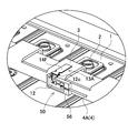
- the battery system has a plurality of battery cells 1, a metal plate bus bar 3 fixed to an electrode terminal 2 of the battery cell 1 and connected to the battery cell 1, and an overcurrent to the bus bar 3. It includes a voltage detection circuit 5 connected via a voltage detection line 4 including protection elements 10, 20, 30, 40, and 50.
- the overcurrent protection elements 10, 20, 30, 40, 50 include a chip fuse 11, a printed circuit board 12 on which the chip fuse 11 is surface-mounted, an external connection portion 13 connected to the printed circuit board 12, and a printed circuit board.
- the insulating layer 15 provided on the 12 is provided.
- the printed circuit board 12 is provided with a conductive portion 12B on the surfaces of the insulating substrates 12A and 12C, and the external connection portion 13 is electrically connected to the conductive portion 12B of the printed circuit board 12.
- the chip fuse 11 is electrically connected to the conductive portion 12B, the chip fuse 11 is connected to the external connection portion 13 via the conductive portion 12B, and the external connection portion 13 is connected to the voltage detection line 4.
- the overcurrent protection element and the battery system of the present invention have a feature that the time and effort for connecting the overcurrent protection element can be simplified, contact failure at the time of connection can be suppressed, and reliability can be improved.
- FIG. 7 It is a circuit diagram of the battery system which concerns on one Embodiment of this invention. It is an enlarged perspective view of the battery system which concerns on one Embodiment of this invention. It is a perspective view of the overcurrent protection element which concerns on one Embodiment of this invention. It is an exploded perspective view of the overcurrent protection element shown in FIG. It is a perspective view of the overcurrent protection element which concerns on other embodiment of this invention. It is a perspective view of the overcurrent protection element which concerns on other embodiment of this invention. It is an exploded perspective view of the overcurrent protection element shown in FIG. It is sectional drawing which shows another example of the insulating plastic molded body. It is a top view which shows the manufacturing process of the overcurrent protection element shown in FIG. 7.
- the overcurrent protection element of the first invention of the present invention includes a chip fuse, a printed circuit board on which the chip fuse is surface-mounted, an external connection portion connected to the printed circuit board, and an insulating layer provided on the printed circuit board.
- the printed circuit board is provided with a conductive portion on the surface of the insulating substrate, the external connection portion is electrically connected to the conductive portion of the printed circuit board, the chip fuse is electrically connected to the conductive portion, and the chip fuse is conductive. It is connected to the external connection part via the part.
- a chip fuse is surface-mounted on a printed circuit board to insulate the surface without using a crimp terminal or a heat-shrinkable tube having a caulking structure, and an external connection portion is provided on the conductive part of the printed circuit board. Since this external connection can be electrically connected to the voltage detection line of the battery system, it can be easily placed in a narrow space to simplify the assembly process, and there is no need to use a crimping terminal for crimping. It has the advantage of improving reliability by suppressing poor contact at the time of connection that occurs at terminals and the like over time.
- the chip fuse can be mounted on the printed circuit board, the external connection part can be electrically connected to the conductive part of the printed circuit board, and the voltage detection line can be connected to the external connection part, the voltage detection line can be used while using a small chip fuse. It also realizes the feature that the electric connection can be easily and surely stable, and the chip fuse can be protected by the printed circuit board or the insulating layer.
- the insulating substrate is a flat hard substrate.
- the hard substrate can stably connect the external connection portion.
- the insulating substrate is a flexible flexible substrate. Flexible boards can be easily placed in a narrow space.
- the overcurrent protection element of the fourth invention of the present invention is an insulating plastic molded body in which an insulating layer is connected to the surface of a printed circuit board.
- the above-mentioned overcurrent protection element has a feature that the printed circuit board, the chip fuse, and the external connection portion can be protected by the insulating layer of the insulating plastic molded body.
- the external connection portion is composed of a pair of the first external connection portion and the second external connection portion, and the first external connection portion is a metal plate.
- the overcurrent protection element of the sixth invention of the present invention has a plate shape in which a metal plate is connected to a bus bar fixed to an electrode terminal of a battery constituting a battery system.
- the overcurrent protection element of the seventh invention of the present invention has a second external connection portion as either a metal plate or a lead wire soldered to a conductive portion of a printed circuit board.
- the overcurrent protection element of the eighth invention of the present invention has a second external connection portion as a metal plate soldered to a conductive portion of a printed circuit board and a lead wire connected to the metal plate.
- the insulating plastic molded body has an opening window for exposing the chip fuse, and the opening window is covered with an insulating material.
- the insulating plastic molded body has a holding portion of an external connection portion.
- the above-mentioned overcurrent protection element has a feature that the connecting portion between the printed circuit board and the external connecting portion can be reinforced with an insulating plastic molded body to strengthen the connecting strength between the two.
- an insulating plastic molded body is connected to a printed circuit board in a locking structure.
- an insulating plastic molded body is fixed so as to sandwich both sides of the printed circuit board.
- the overcurrent protection element of the thirteenth invention of the present invention is a connection in which an external connection portion is connected to a voltage detection line that detects the voltage of each battery constituting a battery system formed by connecting a plurality of batteries in series. It is a department.
- the battery system of the fourteenth invention of the present invention includes a plurality of battery cells, a metal plate bus bar fixed to an electrode terminal of the battery cells and connected to the battery cells, and a voltage detection equipped with an overcurrent protection element in the bus bar. It is equipped with a voltage detection circuit connected via a line.
- the overcurrent protection element includes a chip fuse, a printed circuit board on which the chip fuse is surface-mounted, an external connection portion connected to the printed circuit board, and an insulating layer provided on the printed circuit board.
- a conductive portion is provided on the surface of the insulating substrate, the external connection portion is electrically connected to the conductive portion of the printed circuit board, the chip fuse is electrically connected to the conductive portion, and the chip fuse is electrically connected to the conductive portion via the conductive portion.
- the external connection is connected to the voltage detection line.
- the insulating substrate is either a flat hard substrate or a flexible flexible substrate.
- the battery system of the 16th invention of the present invention is an insulating plastic molded body in which an insulating layer is connected to the surface of a printed circuit board.
- the insulating layer is an insulating plastic molded body that holds an external connection portion.
- the battery system 100 shown in the circuit diagram of FIG. 1 includes a plurality of battery cells 1 and a voltage detection circuit 5 that detects the voltage of each battery cell 1.
- the battery system 100 controls the charge / discharge current with each battery voltage detected by the voltage detection circuit 5 to protect the battery and ensure safety.
- the battery system 100 can be used as a power supply device for supplying electric power to a motor for traveling a vehicle, as a power supply device for a server, as a power supply device for a power storage device for storing electric power generated by a solar cell panel, or as a power supply device for midnight power. It is mainly suitable for high-power power sources such as power supply devices for power storage devices that store electricity.
- the battery system 100 includes a control circuit 6 that controls charging / discharging with the battery voltage detected by the voltage detection circuit 5.
- the control circuit 6 cuts off or decreases the charging current when any of the battery voltages exceeds the set value to prevent overcharging of the battery, and on the contrary, discharges when the battery voltage becomes lower than the set value. Protect the battery from over-discharging by prohibiting or reducing the discharge current. Further, when the battery voltage becomes unbalanced, a specific battery is discharged or charged to equalize and suppress the unbalance.
- a metal plate bus bar 3 is fixed to the electrode terminal 2, and the battery cells 1 are connected in series or in parallel.
- the voltage detection circuit 5 is connected to the bus bar 3 via the voltage detection line 4 to detect each battery voltage.
- the voltage detection line 4 has an overcurrent protection element 10 connected in the middle.
- the overcurrent protection element 10 is connected to the voltage detection line 4, for example, in the assembly process, the battery is protected from an excessive short current flowing by the operator by mistake or the skin is damaged and the voltage detection line 4 is short-circuited. Also, ensure safety.
- the overcurrent protection elements 10, 20 and 30 of FIGS. 3 to 7 include a chip fuse 11 that blows due to an overcurrent, a printed circuit board 12 on which the chip fuse 11 is surface-mounted, and an external device that is connected to the printed circuit board 12.
- a connection portion 13 and an insulating layer 15 provided on the printed circuit board 12 are provided.
- the chip fuse 11 is surface-mounted on a printed circuit board 12, and has a rectangular parallelepiped outer shape so that terminals at both ends can be reflow soldered. Terminals are provided at both ends thereof, and a metal wire fuse is internally fused by a set current. Is placed and both ends of the fuse are connected to the terminals.
- the printed circuit board 12 is provided with a conductive portion 12B by adhering a copper foil to the surface of the insulating substrate 12A.
- the insulating substrate 12A is a hard substrate in which an epoxy resin or a phenol resin in which reinforcing fibers are embedded is molded in a flat shape, or a flexible flexible substrate.
- the hard substrate can stably connect the external connection portion 13, and the flexible substrate can be easily arranged in a narrow space.
- the external connection portion 13 is a pair of terminals that are electrically connected to the conductive portion 12B of the printed circuit board 12, and includes a first external connection portion 13A and a second external connection portion 13B.
- the first external connection portion 13A is composed of a conductive metal plate 14.
- the metal plates 14A and 14C shown in the figure have an outer shape provided with a protruding portion 14a connected to the conductive portion 12B.
- the protruding portion 14a is laminated on the surface of the printed circuit board 12, soldered, and electrically connected to the conductive portion 12B.
- the metal plates 14A and 14C are connected to the printed circuit board 12 at a fixed position by soldering the protruding portion 14a to the conductive portion 12B.
- the first external connection portion 13A of the metal plate 14 is fixed to the bus bar 3 of the battery system 100 and electrically connected.
- the bus bar 3 is a metal plate that connects the battery cells 1 constituting the battery system 100 in series or in parallel.
- the overcurrent protection element 10 in which the first external connection portion 13A is laminated and fixed on the bus bar 3 is surely and stably fixed in a fixed position of the battery cell 1, and is also stably and electrically connected with a small electric resistance. Will be done.
- the first external connection portion 13A fixed to the bus bar 3 is fixed by welding or screwed. Further, the first external connection portion 13A can be fixed to the bus bar 3 by another method such as a caulking structure.
- the second external connection portion 13B is also a conductive metal plate 14.
- the second external connecting portion 13B which is the metal plates 14B and 14D, also has the protruding portion 14a laminated on the printed circuit board 12 and fixed by soldering as an outer shape having the protruding portion 14a.
- the metal plate 14B of the second external connection portion 13B shown in FIG. 3 is provided with a through hole 14b.
- the second external connection portion 13B, which is the metal plate 14B having the through hole 14b, can be fixed by screwing the connection terminal 7 provided at the end of the lead wire 4A of the voltage detection line 4. Further, as shown in FIG.
- the second external connection portion 13B of the metal plate 14D can be electrically connected by laser welding the lead wire 4A of the voltage detection line 4 to the surface or ultrasonically connecting the lead wire 4A. ..
- the overcurrent protection element 30 uses a part of the conductive portion 12B provided on the surface of the printed circuit board 12 as the second external connection portion 13B, and directly leads the voltage detection line 4 here.
- the wire 4A can also be soldered and electrically connected.
- the overcurrent protection elements 10, 20 and 30 shown in FIGS. 3 to 7 have the widths of the metal plates 14A and 14C which are the first external connection portions 13A and the metal plates 14D which are the second external connection portions 13B.
- the width is the same as the width of the rectangular printed circuit board 12, and the metal plates 14 are arranged at the end portions of the printed circuit board 12 in the longitudinal direction so that the metal plates 14 do not project to both sides of the printed circuit board 12.
- These overcurrent protection elements 10, 20 and 30 have a wide metal plate 14 so as to have an outer shape that can be reliably and stably connected to the bus bar 3 and the voltage detection line 4, but are compact and have a narrow battery system 100. There is a feature that it can be placed comfortably in the space.
- the width of the metal plate 14B which is the second external connection portion 13B, is made smaller than the width of the rectangular printed circuit board 12, and the metal plate 14 is printed.
- the shape is such that it does not protrude on both sides of the substrate 12.
- the overcurrent protection element may have a more compact outer shape by making the width of the metal plate, which is the first external connection portion, narrower than that of the printed circuit board.
- the surface of the printed circuit board 12 is insulated by using the insulating layer 15 as the insulating plastic molded bodies 16 and 26.
- the insulating layer 15 is not necessarily limited to the insulating plastic molded bodies 16 and 26.
- a potting resin is applied to the surface of the printed circuit board 12. It is possible to form all other structures capable of insulating the substrate surface by laminating an insulating material on the surface of the printed circuit board 12, such as coating and providing an insulating layer 15.
- the insulating plastic molded bodies 16 and 26 are molded into a shape substantially equal to the outer shape of the rectangular printed circuit board 12, and are laminated on the surface of the printed circuit board 12 to insulate the surface of the printed circuit board 12.
- the insulating layers 15 of the insulating plastic molded bodies 16 and 26 are laminated and fixed on the surface of the printed circuit board 12 to reinforce the printed circuit board 12.
- the insulating plastic molded bodies 16 and 26 are fixed to the printed circuit board 12 with a locking structure, or are fixed by sandwiching the printed circuit board 12 from both sides, and are further adhered and fixed to the surface of the printed circuit board 12.
- the insulating plastic molded body 16 fixed to the printed circuit board 12 in the locking structure is provided with locking hooks 18 integrally molded on both sides.
- the locking hook 18 has a locking portion 18A inside which the printed circuit board 12 can be locked.
- the insulating plastic molded body 16 is fixed to the printed circuit board 12 by locking the lower surface of the printed circuit board 12 with the locking hook 18.
- FIG. 8 shows an example of the insulating plastic molded body 36 fixed by sandwiching the printed circuit board 12.
- the back surface cover 36A arranged on the back surface of the printed circuit board 12 and the insulating cover 36B that insulates the front surface are connected by a bendable hinge portion 36C.
- the hinge portion 36C is thinly molded so that it can be bent, and is integrally molded with the back surface cover 36A and the insulating cover 36B.
- the insulating plastic molded body 36 is provided with a locking hook 18 at the tip of the insulating cover 36B, and is locked with the back surface cover 36A, the hinge portion 36C, and the insulating cover 36B covering the surface of the printed circuit board 12. The hook 18 is locked to the back cover 36A and fixed to the printed circuit board 12.
- the insulating plastic molded bodies 16 and 36 shown in FIGS. 3, 4, 7, and 8 are provided with an opening window 17 for guiding the chip fuse 11 surface-mounted on the printed circuit board 12 and the external connection portion 13. Since the insulating plastic molded bodies 16 and 36 having this shape can guide the members that are surface-mounted and project from the surface of the printed circuit board 12 into the inside of the opening window 17, the entire surface can be thinned to insulate the surface of the printed circuit board 12.
- the opening window 17 is filled with the insulating material 21, that is, the insulating material 21 covers and insulates the surfaces of the chip fuse 11 and the external connection portion 13 arranged inside.
- the insulating plastic molded body 16 is provided with the holding portion 19 of the external connection portion 13.
- the holding portion 19 is a holding convex portion 19A, 19B protruding toward the surface of the external connecting portion 13.
- the holding convex portions 19A and 19B hold the metal plates 14A and 14B, which are the external connecting portions 13, in place by sandwiching them with the printed circuit board 12.
- the holding portion 19 is integrally molded with the insulating plastic molded body 16 and is located on the surfaces of the metal plates 14A and 14B so that the protruding portions 14a of the metal plates 14A and 14B are peeled off from the printed circuit board 12. To prevent.
- the overcurrent protection element 30 shown in FIG. 7 a part of the conductive portion 12B provided on the surface of the printed circuit board 12 is used as the second external connection portion without providing the metal plate on the second external connection portion 13B.
- the lead wire 4A of the voltage detection line 4 is directly soldered, and the holding convex portion 19B integrally molded with the insulating plastic molded body 16 is used as the holding portion 19 for holding the lead wire 4A in a fixed position. It's working. As a result, peeling of the lead wire 4A soldered to the conductive portion 12B is effectively prevented.
- the insulating plastic molded body 26 of FIGS. 5 and 6 has a box shape with an upper opening so that the printed circuit board 12 can be stored inside.
- the insulating plastic molded body 26 includes a peripheral wall 27 along the outer periphery of the printed circuit board, and the peripheral wall 27 is made higher than the thickness of the printed circuit board 12. Further, in the insulating plastic molded body 26 of FIG. 6, the peripheral walls 27 at both ends are partially cut off to form positioning recesses 28 for guiding the metal plates 14C and 14D which are the external connection portions 13.
- the insulating plastic molded body 26 in the figure has fitting protrusions 29 that guide the peripheral walls 27 on both sides of the positioning recess 28 to the fitting recesses 14c provided on both sides of the metal plates 14C and 14D.
- the printed circuit board 12 housed inside is fixed in a fixed position by a locking structure or by adhering, and the fitting protrusions 29 on both sides of the positioning recess 28 are fixed to the metal plate 14C.
- the metal plates 14C and 14D, which are the external connecting portions 13, are connected to the fixed positions by fitting the fitting recesses 14c provided on both sides of the 14D.
- the protruding portions 14a of the metal plates 14C and 14D can be laminated and soldered to the conductive portion 12B provided on the surface of the printed circuit board 12 while being accurately positioned.
- the overcurrent protection element 20 of FIGS. 5 and 6 is the surface of the printed circuit board 12 housed in the insulating plastic molded body 26, and the peripheral wall 27 is filled with an insulating material 21 such as a potting resin.
- the surfaces of the chip fuse 11 and the printed circuit board 12 arranged inside are coated and insulated.
- the overcurrent protection element shown in FIG. 7 is assembled in the process shown in FIG.
- a conductive portion 12B is provided on the surface of the insulating substrate 12A to manufacture the printed circuit board 12.
- the terminals at both ends of the chip fuse 11 are connected to the pair of conductive portions 12B by reflow solder or the like, and the chip fuse 11 is mounted on the printed circuit board 12.
- the metal plate 14A which is the first external connection portion 13A, is soldered and connected to one of the conductive portions 12B of the printed circuit board 12.
- the insulating plastic molded body 16 is fixed to insulate the surface of the printed circuit board 12.
- the lead wire 4A is soldered and connected to the surface of the second external connection portion 13B.
- the overcurrent protection element 30 of FIG. 7 shows the assembly process of the overcurrent protection element 30 of FIG. 7, but the overcurrent protection element can be assembled by soldering or welding a metal plate to the second external connection portion.
- the metal plate 14 serving as the external connection portion 13 is arranged outside the rectangular printed circuit board 12 in the longitudinal direction, or is connected to the second external connection portion 13B.
- the lead wire 4A is pulled out in the longitudinal direction of the printed circuit board 12.
- the overcurrent protection elements 10, 20, and 30 having this structure can be arranged in a narrow space as an elongated shape as a whole.
- the overcurrent protection element connects the metal plate 14 serving as the external connection portion 13 and the lead wire 4A connected to the external connection portion 13 in the lateral direction with respect to the longitudinal direction of the printed circuit board 12, that is, It can also be pulled out in the short direction.
- the overcurrent protection element 40 shown in FIG. 10 connects the metal plate 14E, which is the first external connection portion 13A, to the rectangular printed circuit board 12 so as to project laterally. Further, the lead wire 4A connected to the second external connection portion 13B is also arranged so as to be pulled out in the lateral direction with respect to the printed circuit board 12. Therefore, the insulating plastic molded body 46 that insulates the surface of the printed circuit board 12 is provided with holding protrusions 19A and 19B so as to hold the metal plate 14E and the lead wire 4A that are laterally connected to the printed circuit board 12. There is.
- the overcurrent protection element 40 having this structure is selectively used according to the usage conditions when the arrangement of the overcurrent protection element is restricted, such as when the external connection portion 13 and the lead wire 4A cannot be arranged in a straight line. Will be done.
- the overcurrent protection element can be used by bending the insulating substrate as a flexible insulating substrate 12C.
- the overcurrent protection element 50 in these figures has a protruding connection portion 12c that is a part of the insulating substrate 12C and a first external connection fixed to the protruding connection portion 12c.
- the metal plate 14F, which is the portion 13A, is provided so as to project laterally from the rectangular printed circuit board 12. Further, the lead wire 4A connected to the second external connection portion 13B is pulled out in the longitudinal direction of the printed circuit board 12.
- the insulating plastic molded body 56 shown in the figure is provided with a holding recess 57 for arranging the lead wire 4A at a fixed position.
- the overcurrent protection element 50 can be used by bending the flexible insulating substrate 12C. As shown in FIG. 12, the overcurrent protection element 50 having this structure bends the projecting connection portion 12c protruding in the lateral direction of the insulating substrate 12C, and uses the metal plate 14F, which is the first external connection portion 13A, as a battery cell. It can be used by welding or soldering to the bus bar 3 connected to the electrode terminal 2 of 1.
- the first external connection portion 13A is laminated and fixed on the bus bar 3 of the battery system 100, and the second external connection portion 13B is fixed to the voltage detection line 4. It is connected to the lead wire 4A of the above and is arranged in the middle of the voltage detection line 4.
- the battery system 100 detects each battery voltage by the voltage detection line 4 connecting the overcurrent protection elements 10, 20, 30, 40, 50 in the middle, and controls the charge / discharge current by the control circuit 6.
- the battery cell 1 is safely charged and discharged while protecting each battery cell 1.
- the overcurrent protection element of the present invention is a protection element used in a battery system to protect a battery, and is suitably used as a protection element provided with a fuse that is blown by an excessive current.
- the battery system of the present invention is a battery system including an overcurrent protection element, and in particular, stores power generated by a power supply device for supplying power to a motor for driving an electric vehicle, a power supply device for a server, and a solar cell panel. It can be suitably used as a high-power power source such as a power supply device for a power storage device for storing electricity at midnight or a power supply device for a power storage device for storing midnight power.
- Fitting recess 15 ... Insulation layer , 16, 26, 36, 46, 56 ... Insulating plastic molded body, 17 ... Opening window, 18 ... Locking hook, 18A ... Locking part, 19 ... Holding part, 19A, 19B ... Holding convex part, 21 ... Insulating material , 27 ... peripheral wall, 28 ... positioning recess, 29 ... fitting convex, 36A ... back cover, 36B ... insulating cover, 36C ... hinge, 57 ... holding recess.
Landscapes
- Chemical & Material Sciences (AREA)
- Chemical Kinetics & Catalysis (AREA)
- Electrochemistry (AREA)
- General Chemical & Material Sciences (AREA)
- Engineering & Computer Science (AREA)
- Manufacturing & Machinery (AREA)
- Power Engineering (AREA)
- Fuses (AREA)
- Battery Mounting, Suspending (AREA)
- Connection Of Batteries Or Terminals (AREA)
- Charge And Discharge Circuits For Batteries Or The Like (AREA)
- Protection Of Static Devices (AREA)
Priority Applications (3)
| Application Number | Priority Date | Filing Date | Title |
|---|---|---|---|
| US17/439,858 US12278395B2 (en) | 2019-03-27 | 2019-12-26 | Overcurrent protection element and battery system |
| JP2021508776A JP7474745B2 (ja) | 2019-03-27 | 2019-12-26 | 過電流保護素子とバッテリーシステム |
| CN201980094613.7A CN113614871B (zh) | 2019-03-27 | 2019-12-26 | 过电流保护元件和电池系统 |
Applications Claiming Priority (2)
| Application Number | Priority Date | Filing Date | Title |
|---|---|---|---|
| JP2019060108 | 2019-03-27 | ||
| JP2019-060108 | 2019-03-27 |
Publications (1)
| Publication Number | Publication Date |
|---|---|
| WO2020194967A1 true WO2020194967A1 (ja) | 2020-10-01 |
Family
ID=72610758
Family Applications (1)
| Application Number | Title | Priority Date | Filing Date |
|---|---|---|---|
| PCT/JP2019/051125 Ceased WO2020194967A1 (ja) | 2019-03-27 | 2019-12-26 | 過電流保護素子とバッテリーシステム |
Country Status (4)
| Country | Link |
|---|---|
| US (1) | US12278395B2 (https=) |
| JP (1) | JP7474745B2 (https=) |
| CN (1) | CN113614871B (https=) |
| WO (1) | WO2020194967A1 (https=) |
Cited By (11)
| Publication number | Priority date | Publication date | Assignee | Title |
|---|---|---|---|---|
| JP2022110744A (ja) * | 2021-01-19 | 2022-07-29 | 株式会社オートネットワーク技術研究所 | 配線モジュール |
| WO2022190837A1 (ja) * | 2021-03-09 | 2022-09-15 | 株式会社オートネットワーク技術研究所 | 回路装置 |
| CN115882169A (zh) * | 2021-09-29 | 2023-03-31 | 远景Aesc日本有限公司 | 电压检测装置以及电池模块 |
| CN115882174A (zh) * | 2021-09-29 | 2023-03-31 | 远景Aesc日本有限公司 | 电池模块 |
| EP4160800A3 (en) * | 2021-09-29 | 2023-09-13 | Envision AESC Japan Ltd. | Fuse device and battery module |
| WO2023210373A1 (ja) * | 2022-04-26 | 2023-11-02 | 株式会社オートネットワーク技術研究所 | 配線モジュール |
| JP7561318B1 (ja) * | 2023-06-01 | 2024-10-04 | 株式会社オートネットワーク技術研究所 | ヒューズユニット及びヒューズユニットの製造方法 |
| WO2024248161A1 (ja) * | 2023-06-01 | 2024-12-05 | 株式会社オートネットワーク技術研究所 | 配線モジュール |
| WO2024247346A1 (ja) * | 2023-06-01 | 2024-12-05 | 株式会社オートネットワーク技術研究所 | ヒューズユニット及びヒューズユニットの製造方法 |
| WO2026014310A1 (ja) * | 2024-07-09 | 2026-01-15 | 株式会社オートネットワーク技術研究所 | 電子部品ユニット及び配線モジュール |
| WO2026014305A1 (ja) * | 2024-07-09 | 2026-01-15 | 株式会社オートネットワーク技術研究所 | 電子部品ユニット及び配線モジュール |
Families Citing this family (4)
| Publication number | Priority date | Publication date | Assignee | Title |
|---|---|---|---|---|
| CN114041232B (zh) * | 2021-03-01 | 2024-04-12 | 深圳汝原科技有限公司 | 电芯组件、电池模组及手持式电器设备 |
| CN116471743A (zh) * | 2023-03-30 | 2023-07-21 | 惠州亿纬锂能股份有限公司 | 一种线路保护结构、线路组件及其封装方法、ccs组件 |
| WO2024198008A1 (zh) * | 2023-03-30 | 2024-10-03 | 惠州亿纬锂能股份有限公司 | 一种线路保护结构、线路组件及其封装方法、ccs组件 |
| CN116505203A (zh) * | 2023-05-30 | 2023-07-28 | 惠州亿纬锂能股份有限公司 | 汇流组件和电池模组 |
Citations (6)
| Publication number | Priority date | Publication date | Assignee | Title |
|---|---|---|---|---|
| JPS6054133A (ja) * | 1983-09-02 | 1985-03-28 | 富士通株式会社 | 通信機用保安器 |
| JP2004227797A (ja) * | 2003-01-20 | 2004-08-12 | Uchihashi Estec Co Ltd | 保護素子 |
| JP2005129352A (ja) * | 2003-10-23 | 2005-05-19 | Nec Schott Components Corp | 抵抗付き温度ヒュ−ズ |
| JP2010220377A (ja) * | 2009-03-17 | 2010-09-30 | Panasonic Corp | 蓄電装置 |
| JP2015035281A (ja) * | 2013-08-07 | 2015-02-19 | デクセリアルズ株式会社 | 保護素子、及びこれを用いた保護回路基板 |
| WO2017018213A1 (ja) * | 2015-07-24 | 2017-02-02 | 株式会社オートネットワーク技術研究所 | 電池配線モジュール |
Family Cites Families (15)
| Publication number | Priority date | Publication date | Assignee | Title |
|---|---|---|---|---|
| US7498392B2 (en) * | 2005-01-19 | 2009-03-03 | Nelson Kevin G | Methods and compositions for dielectric materials |
| WO2006112501A1 (ja) * | 2005-04-20 | 2006-10-26 | Matsushita Electric Industrial Co., Ltd. | 二次電池の保護回路、電池パック、及び感熱保護スイッチ装置 |
| EP2408277B1 (de) * | 2010-07-16 | 2016-02-17 | Schurter AG | Sicherungselement |
| JP6012595B2 (ja) * | 2011-03-29 | 2016-10-25 | 三洋電機株式会社 | バッテリモジュール、バッテリシステム、電動車両、移動体、電力貯蔵装置、電源装置および電気機器 |
| JP5952674B2 (ja) * | 2012-08-01 | 2016-07-13 | デクセリアルズ株式会社 | 保護素子及びバッテリパック |
| JP2014093864A (ja) * | 2012-11-02 | 2014-05-19 | Toyota Industries Corp | 電池 |
| US10107867B2 (en) * | 2013-11-12 | 2018-10-23 | Infineon Technologies Ag | Sensor arrangement, battery cell and energy system |
| EP3092669A4 (en) * | 2014-01-08 | 2017-06-21 | MiniPumps, LLC | Stacked battery tray structure and related methods |
| CN105098132A (zh) * | 2014-05-15 | 2015-11-25 | (株)Itm半导体 | 电池保护电路组件 |
| JP6535309B2 (ja) * | 2016-09-26 | 2019-06-26 | 矢崎総業株式会社 | 電池監視ユニット |
| JP6712257B2 (ja) * | 2017-11-01 | 2020-06-17 | デクセリアルズ株式会社 | 保護素子、ヒューズ素子 |
| CN108767178A (zh) * | 2018-03-28 | 2018-11-06 | 北京普莱德新能源电池科技有限公司 | 印刷电路板pcb托盘及电池模组 |
| JP2019033090A (ja) * | 2018-10-03 | 2019-02-28 | 株式会社オートネットワーク技術研究所 | 電池配線モジュール |
| JP2020106330A (ja) * | 2018-12-26 | 2020-07-09 | デクセリアルズ株式会社 | 電流検知素子、電流検知素子複合体および保護回路 |
| JP7567389B2 (ja) * | 2020-11-17 | 2024-10-16 | 株式会社オートネットワーク技術研究所 | 配線モジュール |
-
2019
- 2019-12-26 WO PCT/JP2019/051125 patent/WO2020194967A1/ja not_active Ceased
- 2019-12-26 CN CN201980094613.7A patent/CN113614871B/zh active Active
- 2019-12-26 JP JP2021508776A patent/JP7474745B2/ja active Active
- 2019-12-26 US US17/439,858 patent/US12278395B2/en active Active
Patent Citations (6)
| Publication number | Priority date | Publication date | Assignee | Title |
|---|---|---|---|---|
| JPS6054133A (ja) * | 1983-09-02 | 1985-03-28 | 富士通株式会社 | 通信機用保安器 |
| JP2004227797A (ja) * | 2003-01-20 | 2004-08-12 | Uchihashi Estec Co Ltd | 保護素子 |
| JP2005129352A (ja) * | 2003-10-23 | 2005-05-19 | Nec Schott Components Corp | 抵抗付き温度ヒュ−ズ |
| JP2010220377A (ja) * | 2009-03-17 | 2010-09-30 | Panasonic Corp | 蓄電装置 |
| JP2015035281A (ja) * | 2013-08-07 | 2015-02-19 | デクセリアルズ株式会社 | 保護素子、及びこれを用いた保護回路基板 |
| WO2017018213A1 (ja) * | 2015-07-24 | 2017-02-02 | 株式会社オートネットワーク技術研究所 | 電池配線モジュール |
Cited By (35)
| Publication number | Priority date | Publication date | Assignee | Title |
|---|---|---|---|---|
| JP7576223B2 (ja) | 2021-01-19 | 2024-10-31 | 株式会社オートネットワーク技術研究所 | 配線モジュール |
| JP7816591B2 (ja) | 2021-01-19 | 2026-02-18 | 株式会社オートネットワーク技術研究所 | 配線モジュール |
| JP7768439B2 (ja) | 2021-01-19 | 2025-11-12 | 株式会社オートネットワーク技術研究所 | 配線モジュール |
| JP7768320B2 (ja) | 2021-01-19 | 2025-11-12 | 株式会社オートネットワーク技術研究所 | 回路基板 |
| JP2025079829A (ja) * | 2021-01-19 | 2025-05-22 | 株式会社オートネットワーク技術研究所 | 配線モジュール |
| JP2025067997A (ja) * | 2021-01-19 | 2025-04-24 | 株式会社オートネットワーク技術研究所 | 配線モジュール |
| JP2025003509A (ja) * | 2021-01-19 | 2025-01-09 | 株式会社オートネットワーク技術研究所 | 回路基板 |
| JP2022110744A (ja) * | 2021-01-19 | 2022-07-29 | 株式会社オートネットワーク技術研究所 | 配線モジュール |
| WO2022190837A1 (ja) * | 2021-03-09 | 2022-09-15 | 株式会社オートネットワーク技術研究所 | 回路装置 |
| JP2022137860A (ja) * | 2021-03-09 | 2022-09-22 | 株式会社オートネットワーク技術研究所 | 回路装置 |
| JP7578028B2 (ja) | 2021-03-09 | 2024-11-06 | 株式会社オートネットワーク技術研究所 | 回路装置 |
| JP7596336B2 (ja) | 2021-09-29 | 2024-12-09 | 株式会社Aescジャパン | 電池モジュール |
| EP4160800A3 (en) * | 2021-09-29 | 2023-09-13 | Envision AESC Japan Ltd. | Fuse device and battery module |
| CN115882174B (zh) * | 2021-09-29 | 2026-04-14 | 株式会社Aesc日本 | 电池模块 |
| US12597685B2 (en) | 2021-09-29 | 2026-04-07 | Aesc Japan Ltd. | Voltage detection device and battery module |
| CN115882169A (zh) * | 2021-09-29 | 2023-03-31 | 远景Aesc日本有限公司 | 电压检测装置以及电池模块 |
| CN115882174A (zh) * | 2021-09-29 | 2023-03-31 | 远景Aesc日本有限公司 | 电池模块 |
| EP4160786A1 (en) * | 2021-09-29 | 2023-04-05 | Envision AESC Japan Ltd. | Voltage detection device and battery module |
| JP2023050127A (ja) * | 2021-09-29 | 2023-04-10 | 株式会社エンビジョンAescジャパン | 電池モジュール |
| JP2023161743A (ja) * | 2022-04-26 | 2023-11-08 | 株式会社オートネットワーク技術研究所 | 配線モジュール |
| JP7769875B2 (ja) | 2022-04-26 | 2025-11-14 | 株式会社オートネットワーク技術研究所 | 配線モジュール |
| WO2023210373A1 (ja) * | 2022-04-26 | 2023-11-02 | 株式会社オートネットワーク技術研究所 | 配線モジュール |
| JP2024173846A (ja) * | 2023-06-01 | 2024-12-12 | 株式会社オートネットワーク技術研究所 | ヒューズユニット及びヒューズユニットの製造方法 |
| JP2025041905A (ja) * | 2023-06-01 | 2025-03-26 | 株式会社オートネットワーク技術研究所 | ヒューズユニット |
| JP2024173928A (ja) * | 2023-06-01 | 2024-12-13 | 株式会社オートネットワーク技術研究所 | ヒューズユニット及びヒューズユニットの製造方法 |
| JP2024173927A (ja) * | 2023-06-01 | 2024-12-13 | 株式会社オートネットワーク技術研究所 | ヒューズユニット及びヒューズユニットの製造方法 |
| JP7561318B1 (ja) * | 2023-06-01 | 2024-10-04 | 株式会社オートネットワーク技術研究所 | ヒューズユニット及びヒューズユニットの製造方法 |
| JP7803380B2 (ja) | 2023-06-01 | 2026-01-21 | 株式会社オートネットワーク技術研究所 | ヒューズユニット及びヒューズユニットの製造方法 |
| JP7803381B2 (ja) | 2023-06-01 | 2026-01-21 | 株式会社オートネットワーク技術研究所 | ヒューズユニット及びヒューズユニットの製造方法 |
| WO2024248160A1 (ja) * | 2023-06-01 | 2024-12-05 | 株式会社オートネットワーク技術研究所 | 電子部品ユニット及び電子部品ユニットの製造方法 |
| WO2024247346A1 (ja) * | 2023-06-01 | 2024-12-05 | 株式会社オートネットワーク技術研究所 | ヒューズユニット及びヒューズユニットの製造方法 |
| WO2024248161A1 (ja) * | 2023-06-01 | 2024-12-05 | 株式会社オートネットワーク技術研究所 | 配線モジュール |
| JP7850379B2 (ja) | 2023-06-01 | 2026-04-23 | 株式会社オートネットワーク技術研究所 | ヒューズユニット及びヒューズユニットの製造方法 |
| WO2026014310A1 (ja) * | 2024-07-09 | 2026-01-15 | 株式会社オートネットワーク技術研究所 | 電子部品ユニット及び配線モジュール |
| WO2026014305A1 (ja) * | 2024-07-09 | 2026-01-15 | 株式会社オートネットワーク技術研究所 | 電子部品ユニット及び配線モジュール |
Also Published As
| Publication number | Publication date |
|---|---|
| CN113614871A (zh) | 2021-11-05 |
| CN113614871B (zh) | 2025-11-14 |
| JPWO2020194967A1 (https=) | 2020-10-01 |
| US20220190451A1 (en) | 2022-06-16 |
| JP7474745B2 (ja) | 2024-04-25 |
| US12278395B2 (en) | 2025-04-15 |
Similar Documents
| Publication | Publication Date | Title |
|---|---|---|
| WO2020194967A1 (ja) | 過電流保護素子とバッテリーシステム | |
| EP2378594B1 (en) | Secondary battery | |
| KR101084783B1 (ko) | 이차 전지 및 그의 제조 방법 | |
| US10342134B2 (en) | Printed circuit board and a method of bonding electrode lead of battery to printed circuit board | |
| US20210375510A1 (en) | Shunt Resistor Module Having Screw Coupling Structure | |
| JP2001256937A (ja) | 組電池及び電池パック | |
| US20140204544A1 (en) | Flat wiring member and manufacturing method thereof | |
| KR101210093B1 (ko) | 연결탭 및 이를 구비한 이차전지 | |
| US20240014501A1 (en) | Wiring module | |
| JP7589925B2 (ja) | ヒューズラインを備えるフィルム型ケーブル | |
| US20100129687A1 (en) | Circuit board for secondary battery and secondary battery with the circuit board | |
| KR102331064B1 (ko) | 전지 팩 | |
| KR101282492B1 (ko) | 배터리 팩 | |
| JP3244400B2 (ja) | パック電池 | |
| US20240243420A1 (en) | Wiring module and busbar unit | |
| JP2019129055A (ja) | 蓄電モジュール | |
| KR20160123851A (ko) | 홀더를 갖는 전지 모듈 | |
| KR20080039093A (ko) | 이차전지 | |
| KR102364930B1 (ko) | 커버레이를 포함하는 전지팩 | |
| US9362543B2 (en) | Battery pack | |
| JP2014191886A (ja) | 分岐配線用フラットケーブル並びにこれを用いた分岐配線方法及び分岐配線構造体 | |
| KR20150121089A (ko) | 보호 소자 및 전자 기기 | |
| JP5046568B2 (ja) | 電池パック | |
| KR102273776B1 (ko) | 배터리 팩 | |
| KR20150058807A (ko) | 배터리팩 |
Legal Events
| Date | Code | Title | Description |
|---|---|---|---|
| 121 | Ep: the epo has been informed by wipo that ep was designated in this application |
Ref document number: 19920855 Country of ref document: EP Kind code of ref document: A1 |
|
| ENP | Entry into the national phase |
Ref document number: 2021508776 Country of ref document: JP Kind code of ref document: A |
|
| WWE | Wipo information: entry into national phase |
Ref document number: 201980094613.7 Country of ref document: CN |
|
| NENP | Non-entry into the national phase |
Ref country code: DE |
|
| 122 | Ep: pct application non-entry in european phase |
Ref document number: 19920855 Country of ref document: EP Kind code of ref document: A1 |
|
| WWG | Wipo information: grant in national office |
Ref document number: 17439858 Country of ref document: US |