WO2020189229A1 - 透明電極付き基板の製造方法 - Google Patents
透明電極付き基板の製造方法 Download PDFInfo
- Publication number
- WO2020189229A1 WO2020189229A1 PCT/JP2020/008488 JP2020008488W WO2020189229A1 WO 2020189229 A1 WO2020189229 A1 WO 2020189229A1 JP 2020008488 W JP2020008488 W JP 2020008488W WO 2020189229 A1 WO2020189229 A1 WO 2020189229A1
- Authority
- WO
- WIPO (PCT)
- Prior art keywords
- oxide layer
- transparent
- film
- substrate
- forming
- Prior art date
- Legal status (The legal status is an assumption and is not a legal conclusion. Google has not performed a legal analysis and makes no representation as to the accuracy of the status listed.)
- Ceased
Links
Images

Classifications
-
- B—PERFORMING OPERATIONS; TRANSPORTING
- B32—LAYERED PRODUCTS
- B32B—LAYERED PRODUCTS, i.e. PRODUCTS BUILT-UP OF STRATA OF FLAT OR NON-FLAT, e.g. CELLULAR OR HONEYCOMB, FORM
- B32B9/00—Layered products comprising a layer of a particular substance not covered by groups B32B11/00 - B32B29/00
-
- C—CHEMISTRY; METALLURGY
- C23—COATING METALLIC MATERIAL; COATING MATERIAL WITH METALLIC MATERIAL; CHEMICAL SURFACE TREATMENT; DIFFUSION TREATMENT OF METALLIC MATERIAL; COATING BY VACUUM EVAPORATION, BY SPUTTERING, BY ION IMPLANTATION OR BY CHEMICAL VAPOUR DEPOSITION, IN GENERAL; INHIBITING CORROSION OF METALLIC MATERIAL OR INCRUSTATION IN GENERAL
- C23C—COATING METALLIC MATERIAL; COATING MATERIAL WITH METALLIC MATERIAL; SURFACE TREATMENT OF METALLIC MATERIAL BY DIFFUSION INTO THE SURFACE, BY CHEMICAL CONVERSION OR SUBSTITUTION; COATING BY VACUUM EVAPORATION, BY SPUTTERING, BY ION IMPLANTATION OR BY CHEMICAL VAPOUR DEPOSITION, IN GENERAL
- C23C14/00—Coating by vacuum evaporation, by sputtering or by ion implantation of the coating forming material
- C23C14/06—Coating by vacuum evaporation, by sputtering or by ion implantation of the coating forming material characterised by the coating material
- C23C14/08—Oxides
-
- C—CHEMISTRY; METALLURGY
- C23—COATING METALLIC MATERIAL; COATING MATERIAL WITH METALLIC MATERIAL; CHEMICAL SURFACE TREATMENT; DIFFUSION TREATMENT OF METALLIC MATERIAL; COATING BY VACUUM EVAPORATION, BY SPUTTERING, BY ION IMPLANTATION OR BY CHEMICAL VAPOUR DEPOSITION, IN GENERAL; INHIBITING CORROSION OF METALLIC MATERIAL OR INCRUSTATION IN GENERAL
- C23C—COATING METALLIC MATERIAL; COATING MATERIAL WITH METALLIC MATERIAL; SURFACE TREATMENT OF METALLIC MATERIAL BY DIFFUSION INTO THE SURFACE, BY CHEMICAL CONVERSION OR SUBSTITUTION; COATING BY VACUUM EVAPORATION, BY SPUTTERING, BY ION IMPLANTATION OR BY CHEMICAL VAPOUR DEPOSITION, IN GENERAL
- C23C14/00—Coating by vacuum evaporation, by sputtering or by ion implantation of the coating forming material
- C23C14/22—Coating by vacuum evaporation, by sputtering or by ion implantation of the coating forming material characterised by the process of coating
- C23C14/34—Sputtering
-
- H—ELECTRICITY
- H01—ELECTRIC ELEMENTS
- H01B—CABLES; CONDUCTORS; INSULATORS; SELECTION OF MATERIALS FOR THEIR CONDUCTIVE, INSULATING OR DIELECTRIC PROPERTIES
- H01B13/00—Apparatus or processes specially adapted for manufacturing conductors or cables
Definitions
- the present invention relates to a method for manufacturing a substrate with a transparent electrode.
- Substrates with transparent electrodes are used for display devices such as touch panels and displays, smart windows such as dimming devices, light emitting devices such as LEDs, and light receiving devices such as solar cells.
- display devices such as touch panels and displays
- smart windows such as dimming devices, light emitting devices such as LEDs, and light receiving devices such as solar cells.
- the electrical characteristics expressed as sheet resistance are important.
- a silicon oxide film as described in Patent Document 1 is formed as a base layer, or plasma treatment with an inert gas as described in Patent Document 2 is performed. It is generally known that (bomberd treatment) is applied.
- Inorganic compounds may be dispersed in the coating layer of the film substrate, but it is generally composed mainly of polymer compounds. It is known that the surface of a film substrate derived from a polymer compound is physically or chemically altered by plasma.
- the polymer compound, the oligomer component, and the low molecular weight component that have been altered as described above are used in the film forming chamber for forming the transparent oxide layer constituting the transparent electrode. It may diffuse into the transparent oxide layer after film formation. For this reason, when a film base material mainly composed of a polymer compound is used, it is more difficult to reduce the resistance of the transparent electrode than when a glass base material is used.
- a fine uneven shape is formed on the surface of the film base material. Therefore, it is difficult to maintain the flatness of the surface of the film substrate.
- Such a fine uneven shape has a great influence on various physical properties of a transparent electrode having a thickness of several tens of nm to several hundreds of nm.
- the fine uneven shape may adversely affect the crystallinity of the transparent electrode material in particular. That is, when a fine uneven shape is formed, it may be difficult to reduce the resistance of the transparent electrode material.
- the film base material may not be durable against plasma.
- acrylic resin dissociation of the main chain or side chain is likely to occur.
- plasma treatment is performed on a film base material made of acrylic resin, a transparent conductive oxide layer is formed due to the formation of uneven shapes on the surface of the film base material and the release of low molecular weight components dissociated by plasma. It may adversely affect the electrical and optical properties of the layer.
- the present invention has been made to solve the above problems. That is, the present inventors have formed a film-forming condition at the time of forming the transparent conductive oxide layer and a transparent base oxide layer suitable for the transparent conductive oxide layer formed under the condition. As a result, it was found that low resistance is possible.
- the present invention relates to the following.
- a method for manufacturing a substrate with a transparent electrode has a transparent oxide layer on the film substrate.
- the film substrate contains a film substrate made of a thermoplastic resin and contains.
- the transparent oxide layer includes a crystalline transparent base oxide layer and an amorphous transparent conductive oxide layer.
- the transparent base oxide layer is on the film substrate side with respect to the transparent conductive oxide layer.
- the manufacturing method is A transparent base oxide layer forming step of forming a transparent base oxide layer on a film base material by a sputtering method at a film forming pressure Pu and an oxygen partial pressure Po at the time of film formation.
- Including Pu, Pc, Pou, and Poc are the following equations (1) and (2): 0.30 ⁇ Pu / Pc ⁇ 0.90 ... (1) 0.30 ⁇ (Pu / Pc) ⁇ (Pou / Poc) ⁇ 1.00 ... (2) Satisfy, manufacturing method.
- the total film thickness of the transparent oxide layer is 20 nm or more and 220 nm or less, and the ratio of the film thickness of the transparent base oxide layer to the total film thickness is 1.4% or more and 8.0% or less [1].
- the oxygen partial pressure Pou at the time of forming the transparent base oxide layer film and the oxygen partial pressure Poc at the time of forming the transparent conductive oxide layer film are expressed by the following formula (3): 0.50 ⁇ Pou / Poc ⁇ 1.50
- the transparent base oxide layer and the transparent conductive oxide layer are formed by using raw materials having the same composition, the raw material is indium tin oxide, and the amount of tin oxide added to the raw material is the weight of indium tin oxide.
- FIG. 1 is a diagram schematically showing a cross section of a substrate 10 with a transparent electrode.
- the substrate 10 with a transparent electrode includes a film substrate 16, a transparent substrate oxide layer 11, and a transparent conductive oxide layer 17 in this order.
- the composite layer composed of the transparent base oxide layer 11 and the transparent conductive oxide layer 17 will be referred to as a transparent oxide layer 18.
- the transparent base oxide layer 11 may be one layer or a plurality of layers. One layer is preferable from the viewpoint of achieving productivity and crystallization in a short time by annealing treatment.
- the film base material 16 is a material (base material: base material) that serves as a base for the substrate 10 with a transparent electrode. As the film base material 16, it is preferable to use the film base material 16 which is transparent in the visible light region.
- the film substrate 16 has a transparent film substrate 13.
- the transparent film substrate 13 is not particularly limited as long as it is transparent at least in the visible light region.
- the thickness of the transparent film substrate 13 is not particularly limited, but is preferably 10 ⁇ m or more and 400 ⁇ m or less, and more preferably 20 ⁇ m or more and 200 ⁇ m or less. Within this range, it is easy to achieve both sufficient durability of the transparent film substrate 13 and the substrate 10 with a transparent electrode and appropriate flexibility.
- the transparent film substrate 13 is within this thickness range, the transparent base oxide layer 11, the transparent conductive oxide layer 17, and the like can be formed by a roll-to-roll method. As a result, the substrate 10 with a transparent electrode is manufactured with high productivity.
- thermoplastic resin is particularly preferable as the material of the transparent film substrate 13.
- the thermoplastic part resin as the material of the transparent film substrate 13 include acrylic resins such as polymethylmethacrylate (PMMA), polyethylene terephthalate (PET), polybutylene terephthalate (PBT), and polyethylene naphthalate (Pethylene naphthalate).
- polyester resins such as PEN
- COP, COC cycloolefin resins
- polycarbonate resins acrylic resins and polycarbonate resins are more preferably used from the viewpoint of excellent transparency.
- the film base material 16 may include the functional layer 14 on one side (front surface or back surface) or both sides of the transparent film substrate 13.
- the functional layer 14 may be a single layer or a plurality of layers.
- Examples of the layers constituting the functional layer 14 include an optical adjustment layer, an antireflection layer, an anti-glare layer, an easy adhesion layer, a stress buffer layer, a hard coat layer, an easy slip layer, an antistatic layer, and a crystallization promoting layer. , Crystallization rate adjusting layer, coating layer and the like.
- An example of the case where the functional layer 14 is a plurality of layers includes, for example, a combination of a hard coat layer and an optical adjustment layer.
- the optical adjustment layers are a transparent film substrate 13 (refractive coefficient: 1.4 to 1.6), a transparent base oxide layer 11 and a transparent conductive oxide layer 17 (refractive coefficient: 1.9 to 2.2).
- a transparent film substrate 13 reffractive coefficient: 1.4 to 1.6
- a transparent base oxide layer 11 By being formed between materials having different refractive coefficients such as, the reflection of light between the transparent film substrate 13 and the transparent base oxide layer 11 is suppressed, the light transmittance is improved, and the light is transmitted. Color adjustment using interference is possible.
- Such an optical adjustment layer may be a single layer or a plurality of layers.
- the average refractive index of the optical adjustment layer represented by the following formula is a value between the refractive index of the transparent film substrate 13 (or the functional layer 14 such as the hard coat layer) and the refractive index of the transparent base oxide layer 11. It is preferable to have.
- n ave denotes the average refractive index
- n i is the refractive index of each layer
- d i is the physical thickness of each layer
- m is the product total.
- the thickness of the hard coat layer is preferably 1 ⁇ m or more and 10 ⁇ m or less, more preferably 3 ⁇ m or more and 8 ⁇ m or less, and even more preferably 5 ⁇ m or more and 8 ⁇ m or less. When the thickness of the hard coat layer is within this range, it is easy to impart appropriate durability and flexibility to the transparent film base material 16.
- the substrate 10 with a transparent electrode has a transparent oxide layer 18 on a film substrate 16.
- the transparent oxide layer 18 has a crystalline transparent base oxide layer 11 and an amorphous transparent conductive oxide layer 17 in this order from the film substrate 16 side.
- crystalline as used herein means that, among the states in which the crystal state of crystal grains and the like can be confirmed, the state includes the order of atomic arrangement such as a lattice image by observation using a transmission electron microscope (TEM). It means a state that can be confirmed. More specifically, a state containing an order of atomic arrangement at a distance of about 5 nm can be said to be crystalline.
- the "amorphous" state is a state in which no clear crystal state such as crystal grains is observed by observation using a transmission electron microscope (TEM) immediately after film formation, or a state in which a granular structure can be confirmed. Even so, it shows a state that does not contain the order of the atomic arrangement. In cross-sectional observation using TEM, crystalline and amorphous can be distinguished by the contrast of the image and the lattice image.
- the transparent base oxide layer 11 is a layer that serves as a base for the transparent conductive oxide layer 17.
- the transparent base oxide layer 11 is crystalline. Since the transparent base oxide layer 11 is crystalline, the influence of plasma at the time of forming the transparent conductive oxide layer 17 is less likely to reach the film base material 16 and the transparent film substrate 13. This is important for thermoplastic resins, which are susceptible to structural transformation under the influence of plasma.
- the raw material of the transparent base oxide layer 11 and the raw material of the transparent conductive oxide layer 17 have the same composition.
- the transparent base oxide layer 11 examples include a layer containing zinc oxide, yttrium oxide, magnesium oxide or indium oxide as a main component. Above all, it is preferable that the transparent base oxide layer 11 is formed by a crystalline thin film containing indium oxide as a main component. As used herein, the term "main component" means that the material is contained in an amount of more than 50% by weight.
- the transparent base oxide layer 11 and the transparent conductive oxide layer 17 are preferably formed using raw materials having the same composition as described above.
- the term "raw material having the same composition” as used herein means that the composition of the sputtering target material when formed by sputtering has not been intentionally changed.
- the sputter target is preferably indium oxide (hereinafter referred to as ITO) to which tin oxide is added.
- ITO indium oxide
- the amount of tin oxide added to ITO is preferably 8.2% by weight or more and 11.2% by weight or less, and 8.6% by weight or more and 11.0% by weight, based on the total of the weight of ITO and the weight of tin oxide. % Or less is more preferable, and 9.0% by weight or more and 10.5% by weight or less is further preferable.
- the amount of tin oxide added having the lowest resistivity of ITO formed on a film substrate is 8.0% by weight or more with respect to the total of the weight of ITO and the weight of tin oxide. It is said to be less than 5.5% by weight. This is partly derived from crystals. That is, it is considered that if the amount of tin oxide added is increased to around 10% by weight, the crystallization of ITO becomes insufficient even if annealing is performed.
- ITO is sufficiently crystallized even with a high tin oxide addition amount such as 10.0% by weight due to the effect of the transparent base oxide layer 11.
- the film thickness of the transparent base oxide layer 11 is preferably 1.4% or more and 3.5% or less with respect to the film thickness of the transparent oxide layer 18.
- the formation of the transparent base oxide layer 11 suppresses the diffusion of components containing carbon atoms and nitrogen atoms, which are crystallization inhibitory components, from the transparent film base material 16 to the transparent conductive oxide layer 17 and the film forming chamber.
- the film thickness of the transparent oxide layer 18 is preferably 40 nm or more and 200 nm or less, and particularly preferably 45 nm or more and 120 nm or less, from the viewpoint of the correlation between the electrical characteristics and the warp of the substrate 10 with the transparent electrode.
- Indium oxide is an oxide whose main component is indium. It is preferable that indium oxide is contained in the transparent base oxide layer 11 as a main component from the viewpoint of controlling the surface free energy of the transparent base oxide layer 11 to an optimum value for forming the transparent conductive oxide layer 17. Indium oxide is preferable from the viewpoint of barrier properties that protect the film against not only chemical factors such as water vapor but also physical factors such as plasma. By making the indium oxide in the transparent base oxide layer 11 crystalline, it is possible to improve the barrier property against plasma. Indium oxide is preferable as the main component of the transparent base oxide layer 11 because it does not contain carbon or nitrogen atoms that can inhibit the crystallization of the transparent conductive oxide layer 17.
- the transparent base oxide layer 11 formed by the method described later can suppress the crystallization of the transparent conductive oxide layer 17 at room temperature as compared with a known base layer material such as silicon oxide.
- Room temperature crystallization means that after the transparent conductive oxide layer 17 is formed, it is left at atmospheric pressure and normal temperature to promote crystallization in a mode different from that at the time of annealing, and crystallization occurs even after annealing. It is a phenomenon that disappears. It is considered that this is due to the effect of controlling the surface free energy of the transparent base oxide layer 11 and the activation energy associated therewith.
- the transparent base oxide layer 11 by the sputtering method using an inorganic compound composed of an oxide containing indium as a main component is compared with, for example, the formation of the base layer by the sputtering method using silicon having a strong bond with oxygen. It is useful.
- silicon binds to oxygen more strongly than indium, it easily becomes an oxygen supersaturated film (layer) in sputtering film formation. As a result, in the transparent conductive oxide layer 17 formed on the oxygen supersaturated layer, crystallization may be excessively promoted and crystallization at room temperature may proceed. However, in the case of indium oxide, there is no such risk.
- the transparent oxide layer 18 From the viewpoint of lattice matching between the transparent base oxide layer 11 and the transparent conductive oxide layer 17, it is preferable to use a compound containing indium oxide as a main component as the transparent oxide layer 18.
- the transparent base oxide layer 11 does not substantially contain silicon oxide.
- substantially not contained means that the content of the substance is less than 1% by weight, preferably less than 0.1% by weight, and particularly preferably 0% by weight.
- the transparent conductive oxide layer 17 is amorphous before the crystallization step by annealing. As described above, it is preferable that the raw material compositions of the transparent conductive oxide layer 17 and the transparent base oxide layer 11 are the same.
- examples of the material of the transparent conductive oxide layer 17 include a material containing zinc oxide, yttrium oxide, magnesium oxide, or indium oxide as a main component, similarly to the transparent base oxide layer 11.
- the transparent conductive oxide layer 17 is preferably formed as an amorphous thin film containing indium oxide as a main component, and more preferably formed using indium oxide (ITO) to which tin oxide is added. preferable.
- the amount of tin oxide added to the sputter target is 8.2% by weight or more and 11.2% by weight or less with respect to the total of the weight of ITO and the weight of tin oxide.
- it is more preferably 8.6% by weight or more and 11.0% by weight or less, and further preferably 9.0% by weight or more and 10.5% by weight or less.
- the carrier density of the transparent conductive oxide layer 17 may be a suitable range of 2 ⁇ 10 20 cm -3 or more and 9 ⁇ 10 20 cm -3 or less, or 6 ⁇ 10 20 cm. It is easy to set a more suitable range of -3 or more and 8 ⁇ 10 20 cm -3 or less.
- the low-resistance transparent oxide layer 18 contributes to, for example, improving the response speed of the capacitive touch panel, improving the uniformity of in-plane brightness of organic EL lighting, and saving power consumption of various optical devices.
- the crystallinity of the transparent oxide layer 18 after crystallization by annealing is preferably 85% or more, more preferably 95% or more. Within such a range of crystallinity, the light absorption by the transparent conductive oxide layer 17 can be reduced, and the change in resistance value due to environmental changes or the like can be suppressed.
- the crystallinity is obtained from the ratio of the area occupied by the crystal grains in the observation field of view during microscopic observation.
- the total thickness of the transparent oxide layer is the sum of the thicknesses of the transparent base oxide layer 11 and the transparent conductive oxide layer 17.
- the total film thickness is preferably 20 nm or more and 220 nm or less, more preferably 20 nm or more and 200 nm or less, and further preferably 20 nm or more and 170 nm or less from the viewpoint that the substrate with the transparent electrode is less likely to warp.
- the ratio of the thickness of the transparent base oxide layer to the layer thickness of the transparent oxide layer is 1 in that the transparent base oxide layer plays a role as a base layer for achieving a low resistance. It is preferably 0.4% or more and 8.0% or less.
- the film base material 16 is prepared.
- the film base material 16 may be a transparent film substrate 13 alone, or may be a film base material 16 in which a functional layer 14 is laminated on the transparent film substrate 13.
- the substrate 10 with a transparent electrode is manufactured by forming the transparent base oxide layer 11 and the transparent oxide layer 18 on the film substrate 16.
- the transparent oxide layer 18 includes a crystalline transparent base oxide layer 11 and an amorphous transparent conductive oxide layer 17.
- the transparent base oxide layer 11 is closer to the film base material 16 than the transparent conductive oxide layer 17.
- the method for manufacturing the substrate 10 with a transparent electrode is as follows. A transparent base oxide layer forming step of forming the transparent base oxide layer 11 on the film base material 16 by a sputtering method at a film forming pressure Pu and an oxygen partial pressure Po at the time of film formation.
- Pu, Pc, Pou, and Poc are represented by the following formulas (1) and (2): 0.30 ⁇ Pu / Pc ⁇ 0.90 ... (1) 0.30 ⁇ (Pu / Pc) ⁇ (Pou / Poc) ⁇ 1.00 ...
- the film of the transparent base oxide layer 11 and the film of the transparent conductive oxide layer 17 are formed by sputtering so as to satisfy the above conditions.
- the step including both the transparent base oxide layer forming step and the transparent conductive oxide layer forming step will also be referred to as a “film forming step”.
- the transparent base oxide layer 11 and the transparent conductive oxide layer 17 are formed on the film base material 16 so as to be in contact with the film base material 16.
- the transparent base oxide layer 11 and the transparent conductive oxide layer 17 are preferably continuously formed by a film forming method (sputtering film forming).
- sputtering film forming the magnetron sputtering method is preferable.
- the strength of the magnet by the magnetron sputtering method is preferably in the range of 700 gauss or more and 1300 gauss or less. Within this range, a decrease in utilization efficiency of the sputtering target due to extreme erosion is suppressed, and a high-quality transparent base oxide layer 11 can be easily formed. It is considered that this is because the discharge voltage is lowered due to the large magnetic field strength. As a result, it is considered that the transparent base oxide layer 11 is formed with low damage to the film base material 16.
- a DC power source, an AC power source, or the like is selected according to the target material.
- the transparent base oxide layer 11 is usually formed on the transparent film base material 16.
- the transparent base oxide layer 11 may be formed on the functional layer 14 included in the transparent film base material 16. Therefore, it is preferable that the transparent base oxide layer 11 is formed so as to reduce damage to the lower layer than the transparent base oxide layer 11, and by extension, the substrate 10 with the transparent electrode.
- As a method of such low-damage film formation in addition to the low-voltage film formation by the strong magnetic field cathode as described above, there is a method of not lowering the film formation pressure too much.
- As a more effective method there is a method of forming a crystalline transparent base oxide layer 11.
- the amount of oxygen (partial pressure) to be introduced is the oxygen partial pressure (Pou) at the time of forming the transparent base oxide layer 11 and the oxygen content at the time of forming the transparent conductive oxide layer 17 from the viewpoint of balance with the electrical characteristics. It is preferable that the pressure (Poc) satisfies the following formula (3). That is, the partial pressure ratio Pou / Poc is preferably 0.50 or more and 1.50 or less. The partial pressure ratio Pou / Poc is more preferably 0.75 or more and 1.25 or less. 0.50 ⁇ Pou / Poc ⁇ 1.50 ... (3)
- the transparent conductive oxide layer 17 is preferably formed continuously on the transparent base oxide layer by a sputtering method, similarly to the transparent base oxide layer 11.
- the transparent conductive oxide layer 17 is preferably formed by a magnetron sputtering method like the transparent base oxide layer 11.
- Sputtered film formation is preferably carried out while introducing an inert gas such as argon or nitrogen and / or a carrier gas containing oxygen gas into the film forming chamber.
- an inert gas such as argon or nitrogen and / or a carrier gas containing oxygen gas
- argon it is preferable to use argon as the inert gas.
- a mixed gas it is preferably a mixed gas of argon and oxygen.
- argon and oxygen may be adjusted in advance to a predetermined mixing ratio, or the respective gases may be mixed after the flow rate is controlled by a flow rate controller (mass flow controller). Good.
- the mixed gas may contain other gases as long as the functions of each layer are not impaired.
- the transparent conductive oxide layer 17 When forming the transparent conductive oxide layer 17, it is preferable to use a mixed gas of oxygen and an inert gas. It is preferable to use argon and oxygen as the mixed gas.
- the oxygen partial pressure Poc when forming the transparent conductive oxide layer 17 is preferably, for example, 1.0 ⁇ 10 -3 Pa or more and 5.0 ⁇ 10 -2 Pa or less, preferably 3.0 ⁇ 10 -3 Pa. More preferably 4.0 ⁇ 10 -2 Pa or less.
- the amount of oxygen supplied is relatively small as described above, many oxygen deficiencies are present in the amorphous film after film formation, and more conductive carriers are generated.
- a method of degassing the film roll in the sputtering apparatus or before putting the apparatus into the apparatus is common.
- the film roll is heated to remove water.
- the transparent base oxide layer 11 under the transparent conductive oxide layer 17 the above-mentioned components are diffused from the transparent film base material 16 when the transparent conductive oxide layer 17 is formed. , Diffusion of the above components after film formation is suppressed.
- the heating and dehydration can be performed by using a chamber different from the film forming chamber. By doing so, the process can be continuously advanced from the dehydration process at a high temperature to the film forming process at a low temperature.
- the relationship (total pressure ratio: Pu / Pc) between the film forming pressure (Pu) of the transparent base oxide layer 11 and the film forming pressure (Pc) of the transparent conductive oxide layer 17 is expressed by the following equation (1). ): 0.30 ⁇ Pu / Pc ⁇ 0.90 ... (1) Meet.
- the relationship between the oxygen partial pressure (Pou) when the transparent base oxide layer 11 is formed and the oxygen partial pressure (Poc) when the transparent conductive oxide layer 17 is formed (partial pressure ratio: Pou / Poc) and the total pressure.
- the range of Pu / Pc in the formula (1) is more preferably 0.40 ⁇ Pu / Pc ⁇ 0.70.
- the range of (Pu / Pc) ⁇ (Pou / Poc) in the formula (2) is particularly preferably 0.30 ⁇ (Pu / Pc) ⁇ (Pou / Poc) ⁇ 0.90.
- the discharge voltage when the transparent base oxide layer 11 is sputtered is not particularly limited as long as the object of the present invention is not impaired. Typically, the discharge voltage is preferably -280 V or more and -255 V or less, that is, the absolute value of the discharge voltage is preferably 255 V to 280 V.
- the transparent film base material 16 is less damaged by sputtering, and high-quality crystalline material can be formed.
- the transparent conductive oxide layer 17 can form a high-quality film.
- the transparent oxide layer 18 may be formed by sputtering to form the total thickness of the desired layer thickness by one film formation or by laminating a plurality of times. It is preferable to form the transparent oxide layer 18 by laminating a plurality of times from the viewpoint of production processing speed or thermal history to the transparent film base material 16.
- the substrate temperature in the sputtering film formation may be within the heat resistance range of the transparent film base material 16.
- the substrate temperature is preferably 60 ° C. or lower, more preferably ⁇ 20 ° C. or higher and 40 ° C. or lower.
- volatilization of organic substances such as water or oligomer components from the transparent film base material 16 is unlikely to occur.
- indium oxide is likely to crystallize.
- the transparent conductive oxide layer 17 is unlikely to be crystallized during film formation. Therefore, it is easy to form the transparent oxide layer 18 having a preferable low resistivity.
- the crystallized transparent oxide layer (crystalline transparent oxide layer) 18 is formed.
- the crystallized transparent oxide layer (crystalline transparent oxide layer) 18 is formed. In this case, it is possible to suppress the formation of defects in the crystal. Therefore, an increase in the resistivity of the transparent oxide layer 18 is suppressed.
- the transparent film base material 16 does not cause a significant dimensional change.
- the transparent base oxide layer 11 and the transparent conductive oxide layer 17 are formed by a roll-to-roll method using a take-up sputtering apparatus.
- a roll-to-roll method By forming a film by the roll-to-roll method, a roll-shaped wound body of a long sheet of a transparent film base material 16 in which an amorphous transparent conductive oxide layer 17 is laminated on the outermost surface can be obtained. .. It is efficient when the transparent base oxide layer 11 and the transparent conductive oxide layer 17 are continuously formed by using a winding sputtering apparatus.
- the substrate 10 with a transparent electrode is manufactured.
- the substrate 10 with a transparent electrode is crystallized by annealing or the like at an arbitrary timing determined by the user or the like.
- the transparent oxide layer 18 having low resistance is obtained due to the crystallization of the transparent conductive oxide layer 17.
- the amorphous transparent oxide layer 18 can be crystallized by annealing the substrate 10 with a transparent electrode provided with the amorphous transparent oxide layer 18 at a temperature of, for example, 120 ° C. or higher and 170 ° C. or lower. it can.
- the annealing is performed in an oxygen-containing atmosphere such as the atmosphere. This is because crystallization proceeds even in a vacuum or under an inert gas atmosphere, but in a low oxygen concentration atmosphere, crystallization tends to take a longer time than in an oxygen atmosphere.
- the crystallized body When the substrate 10 with a transparent electrode is crystallized as a roll-shaped wound body of a long sheet, the crystallized body may be crystallized as it is, or the film is conveyed by roll-to-roll. However, crystallization may be carried out.
- the film which is the substrate 10 with a transparent electrode may be cut out to a predetermined size and crystallized.
- the transparent film base material 16 provided with the transparent oxide layer 18 may be placed as it is in a normal temperature and pressure environment, or may be allowed to stand in a heating chamber or the like.
- the transparent film base material 16 is introduced into a heating furnace while being conveyed, heated, and then wound into a roll again. Even when crystallization is performed at room temperature, the roll-to-roll method may be adopted for the purpose of bringing the transparent oxide layer 18 into contact with oxygen to promote crystallization.
- the substrate 10 with a transparent electrode manufactured as described above is used, for example, as a transparent electrode for a display device such as a touch panel, a display, or a digital signage, or a smart window such as a light control film.
- conductive ink or conductive paste is applied and heat-treated on the substrate 10 with a transparent electrode, and such a conductive member serves as a collecting electrode as wiring for a routing circuit.
- the heat treatment is not particularly limited, and examples thereof include heat treatment using an oven or an IR heater.
- the temperature or time of the heat treatment is appropriately set in consideration of the temperature or time at which the conductive member adheres to the transparent oxide layer 18.
- an oven it is preferable to heat in the range of 120 ° C. or higher and 150 ° C. or lower for 30 minutes or longer and 60 minutes or shorter.
- an IR heater it is preferable to heat it at about 150 ° C. for about 5 minutes.
- the method for forming the wiring for the routing circuit is not limited to the coating / heat treatment of the conductive ink or the conductive paste, and may be, for example, a dry coating method or a photolithography method. In particular, when the wiring for the routing circuit is formed by the photolithography method, the wiring is easily thinned.
- the thickness of the transparent base oxide layer and the transparent conductive oxide layer are values obtained by observing the cross section of the substrate with the transparent electrode with a transmission electron microscope (TEM).
- the sheet resistance of the transparent oxide layer was measured by four-probe pressure welding measurement using a low resistivity meter Loresta GP (MCP-T710, manufactured by Mitsubishi Chemical Corporation).
- the resistivity of the transparent base oxide layer is a value calculated from the result of measuring the surface resistance to the transparent base oxide layer by separately forming a film of only the transparent base oxide layer. Further, the resistivity of the transparent oxide layer after the annealing treatment, which will be described later, was measured in the same manner as the measurement of the surface resistance of the underlying oxide layer.
- Example 1 In the film formation of the transparent base oxide layer and the transparent conductive oxide layer, indium tin oxide (tin oxide content 10% by weight) is used as a target, and the transparent base oxide layer and the transparent conductive oxide are formed by the magnetron sputtering method. The layers were formed continuously. In the film formation of the transparent base oxide layer 11, the strength of the magnet by the magnetron sputtering method was set in the range of 700 gauss or more and 1300 gauss or less at the strongest magnetic field strength on the target surface.
- the substrate temperature in film formation was 20 ° C.
- a film was formed while introducing a mixed gas of oxygen and argon into the apparatus.
- argon and oxygen were supplied in a ratio (volume ratio) of 100:12.
- the total pressure in the film forming chamber was set to 0.33 Pa.
- the power density was 0.5 W / cm 2 (discharge voltage: -265 V).
- the film thickness was 3.0 nm.
- the resistivity of the transparent base oxide layer was 5.5 ⁇ 10 -3 ⁇ cm.
- argon and oxygen were supplied in a ratio of 100: 5 (volume ratio).
- the oxygen partial pressure was 0.029 Pa.
- the total pressure in the film forming chamber was set to 0.60 Pa.
- the power density was 2.5 W / cm 2 (discharge voltage: -279 V).
- the film thickness was 97.0 nm. As a result, the total film thickness of the transparent base oxide layer and the transparent conductive oxide layer was 100.0 nm.
- the sheet resistance was 49 ⁇ / ⁇ after film formation (R0), 20 ⁇ / ⁇ after annealing (R1), and 42 ⁇ / ⁇ after crystallization at room temperature (R2).
- the difference in sheet resistance between after film formation (R0) and after crystallization at room temperature (R2) was 7 ⁇ / ⁇ .
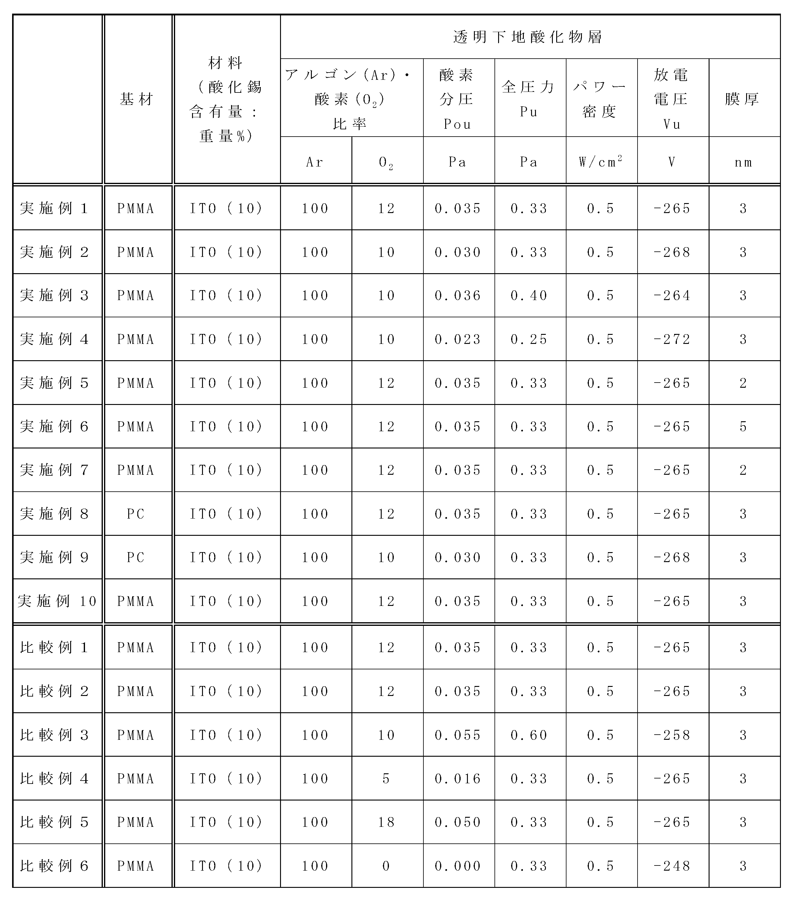
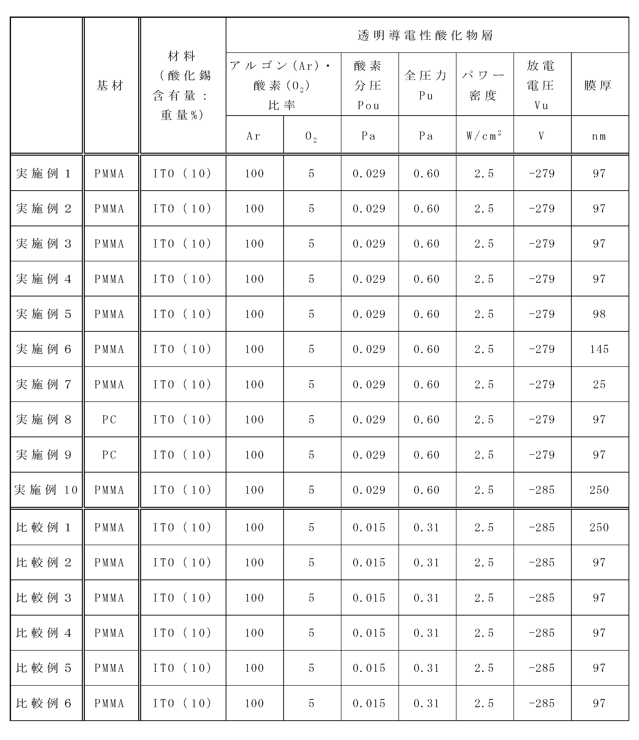
- Examples 2 to 10 and Comparative Examples 1 to 6 Except for changing the film forming conditions to the conditions shown in Tables 1 to 3, film formation and evaluation were carried out in the same manner as in Example 1.
- an acrylic resin film (trade name: Acryplene HBS006, manufactured by Mitsubishi Chemical Corporation) was used as PMMA.
- a polycarbonate film (trade name: Iupiron film, manufactured by Mitsubishi Gas Chemical Company, Inc.) was used as the PC. The thickness of each film was 100 microns.
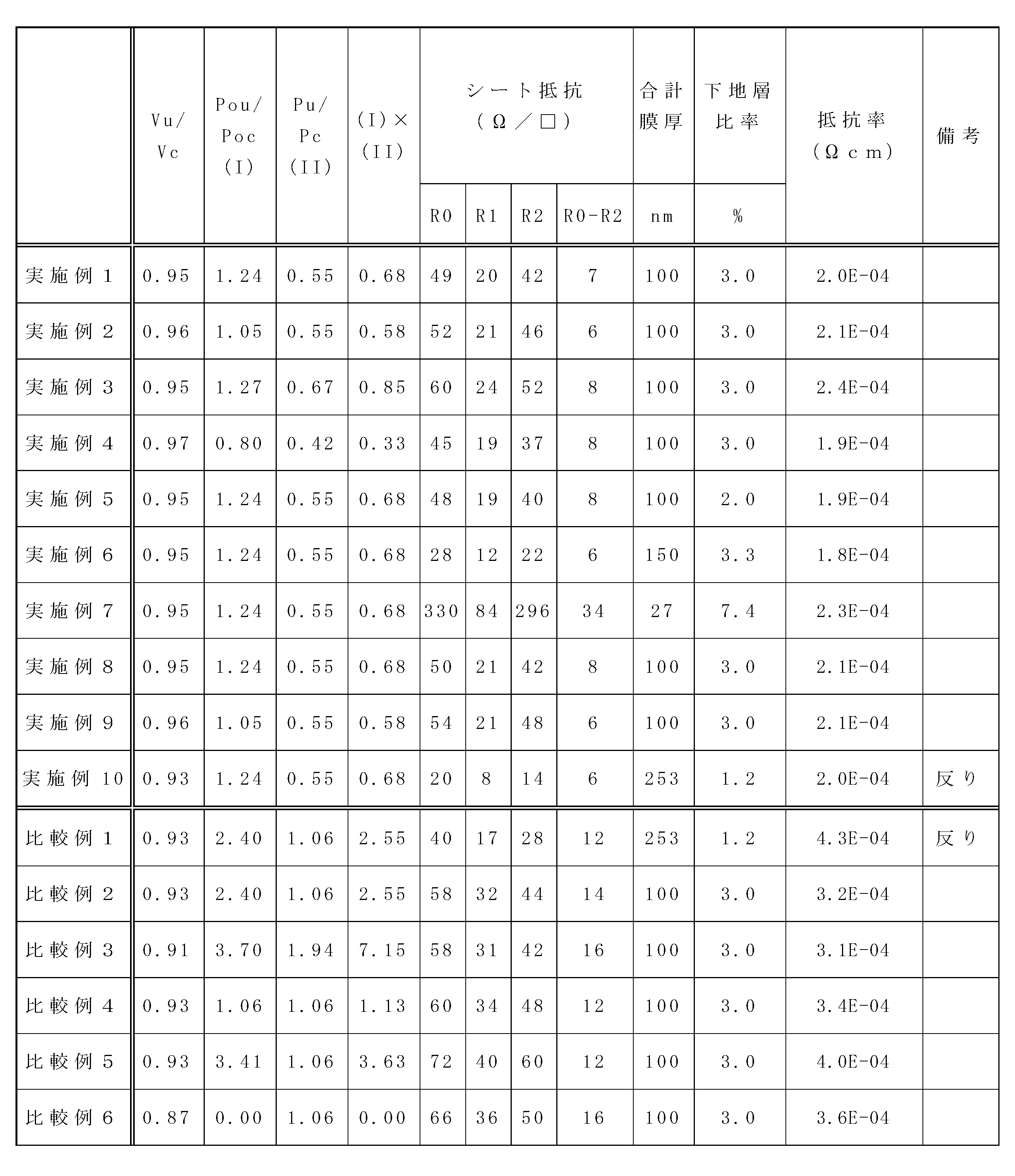
- the transparent base oxide layer and the transparent conductive oxide layer are formed under the condition that Pu, Pc, Pou, and Poc satisfy the above-mentioned formulas (1) and (2), and transparent. Due to the presence of the underlying oxide layer, the resistivity of the transparent oxide layer was 2.5 ⁇ 10 -4 ⁇ cm or less. Focusing on the film-forming pressure of the transparent conductive oxide layer in Examples and Comparative Examples 1 to 6, it was confirmed that the conductivity was improved by increasing the film-forming pressure. It can be said that the improvement of the film forming pressure is effective in reducing the kinetic energy of the particles in the plasma, that is, in reducing the damage to the film substrate. From these results, it was found that a high-quality transparent electrode can be formed by applying the above-mentioned predetermined film forming conditions to the thermoplastic resin film.
- Transparent substrate oxide layer 13 Transparent film substrate [form substrate] 14 Functional layer 16 Transparent film base material [Film base material] 17 Transparent conductive oxide layer 18 Transparent oxide layer
Landscapes
- Chemical & Material Sciences (AREA)
- Engineering & Computer Science (AREA)
- Chemical Kinetics & Catalysis (AREA)
- Materials Engineering (AREA)
- Mechanical Engineering (AREA)
- Metallurgy (AREA)
- Organic Chemistry (AREA)
- Manufacturing & Machinery (AREA)
- Manufacturing Of Electric Cables (AREA)
- Non-Insulated Conductors (AREA)
- Laminated Bodies (AREA)
- Physical Vapour Deposition (AREA)
Abstract
フィルム基材上に低抵抗率の透明電極層としての透明酸化物層を形成できる透明電極付き基板の製造方法を提供する。 透明下地酸化物層を、成膜圧力Pu、成膜時の酸素分圧Pouにてスパッタリング法により形成する、透明下地酸化物層形成工程と、透明下地酸化物層上に、透明導電性酸化物層を、成膜圧力Pc、成膜時の酸素分圧Pocにてスパッタリング法により形成する、透明導電性酸化物層形成工程とを備える方法において、Pu、Pc、Pou、およびPocが所定の式を満たす条件で、透明下地酸化物層と透明導電性酸化物層とを製膜し、透明下地酸化物層と透明導電性酸化物層とを含む透明酸化物層をフィルム基材上に形成する。
Description
本発明は、透明電極付き基板の製造方法に関する。
透明電極付き基板は、タッチパネルおよびディスプレイ等の表示デバイス、調光デバイス等のスマートウィンドウ、LED等の発光デバイス、太陽電池等の受光デバイス等に用いられている。透明電極付き基板では、シート抵抗として表される電気特性が重要である。
フィルム基材上に透明電極を形成する場合、特許文献1に記載されているような酸化ケイ素膜を下地層として形成することや、特許文献2に記載されているような不活性ガスによるプラズマ処理(ボンバード処理)が施されることが一般的に知られている。
フィルム基材は、コーティング層に無機化合物が分散されることがあるが、主として高分子化合物から構成されるのが一般的である。高分子化合物由来のフィルム基材については、プラズマによって表面が物理的または化学的に変質することが知られている。
最近のデバイスの高性能化に伴い、透明電極付きフィルムの性能向上、すなわち透明電極の更なる低抵抗化が重要になってきた。ガラス基材と異なり、フィルム基材の場合には、上述の通り変質した高分子化合物やオリゴマー成分、低分子量成分が、透明電極を構成する透明酸化物層の形成に使用される製膜チャンバー内に拡散したり、製膜後の透明酸化物層に拡散したりすることがある。このような理由により、高分子化合物を主体とするフィルム基材を用いる場合、ガラス基材を用いる場合よりも、透明電極の低抵抗化が困難である。
また、従来知られる方法に従い下地層の形成やボンバード処理を行う場合、フィルム基材の表面に微細な凹凸形状が形成されてしまう。このため、フィルム基材表面の平坦さを維持することが困難である。このような微細な凹凸形状は、厚さが数十nm~数百nmである透明電極に対して種々の物性に大きな影響を及ぼす。微細な凹凸形状は、特に透明電極材料の結晶性に対して悪影響を及ぼすおそれがある。すなわち、微細な凹凸形状が形成される場合、透明電極材料の低抵抗化が困難となるおそれがある。
さらに、フィルム基材を構成する高分子化合物の化学構造によっては、フィルム基材にプラズマに対する耐久性がない可能性がある。例えばアクリル樹脂については、主鎖または側鎖の解離が起こりやすい。このため、アクリル樹脂からなるフィルム基材にプラズマ処理を行う場合、フィルム基材表面に凹凸形状ができたり、プラズマにより解離した低分子量成分の遊離が起こることにより、透明導電性酸化物層形成や層の電気・光学的な特性に悪影響を与えたりする可能性がある。
本発明は、上記の課題を解決するためになされたものである。すなわち、本発明者らは、透明導電性酸化物層形成時の製膜条件、およびその条件で形成される透明導電性酸化物層に対して適した透明下地酸化物層を形成することで、結果として低抵抗化が可能となることを見出した。
本発明者らは、上記課題を解決するために鋭意検討した結果、本発明を完成するに至った。すなわち、本発明は、以下に関する。
[1]透明電極付き基板の製造方法であって、
透明電極付き基板が、フィルム基材上に、透明酸化物層を備え、
フィルム基材が、熱可塑性樹脂からなるフィルム基板を含み、
透明酸化物層は、結晶質の透明下地酸化物層と、非晶質の透明導電性酸化物層とを含み、
透明酸化物層において、透明下地酸化物層が、透明導電性酸化物層よりもフィルム基材側にあり、
製造方法が、
フィルム基材上に、透明下地酸化物層を、成膜圧力Pu、成膜時の酸素分圧Pouにてスパッタリング法により形成する、透明下地酸化物層形成工程と、
透明下地酸化物層上に、透明導電性酸化物層を、成膜圧力Pc、成膜時の酸素分圧Pocにてスパッタリング法により形成する、透明導電性酸化物層形成工程と、
を含み、
Pu、Pc、Pou、およびPocが下記式(1)および(2):
0.30≦Pu/Pc≦0.90・・・(1)
0.30≦(Pu/Pc)×(Pou/Poc)≦1.00・・・(2)
を満たす、製造方法。
[2]熱可塑性樹脂は、アクリル系樹脂またはポリカーボネート系樹脂である、[1]に記載の透明電極付き基板の製造方法。
[3]透明酸化物層の総膜厚は20nm以上220nm以下であり、総膜厚に対する透明下地酸化物層の膜厚の比率が1.4%以上8.0%以下である、[1]または[2]に記載の透明電極付き基板の製造方法。
[4]透明下地酸化物層製膜時の酸素分圧Pouと透明導電性酸化物層製膜時の酸素分圧Pocとが下記式(3):
0.50≦Pou/Poc≦1.50
を満たす、[1]~[3]のいずれか1つに記載の透明電極付き基板の製造方法。
[5]透明下地酸化物層と透明導電性酸化物層とは、同じ組成の原料を用いて製膜され、原料が酸化インジウム錫であり、原料における酸化錫の添加量が酸化インジウム錫の重量と酸化錫の重量との合計に対して8.2重量%以上11.2重量%以下である、[1]~[4]のいずれか1つに記載の透明電極付き基板の製造方法。
透明電極付き基板が、フィルム基材上に、透明酸化物層を備え、
フィルム基材が、熱可塑性樹脂からなるフィルム基板を含み、
透明酸化物層は、結晶質の透明下地酸化物層と、非晶質の透明導電性酸化物層とを含み、
透明酸化物層において、透明下地酸化物層が、透明導電性酸化物層よりもフィルム基材側にあり、
製造方法が、
フィルム基材上に、透明下地酸化物層を、成膜圧力Pu、成膜時の酸素分圧Pouにてスパッタリング法により形成する、透明下地酸化物層形成工程と、
透明下地酸化物層上に、透明導電性酸化物層を、成膜圧力Pc、成膜時の酸素分圧Pocにてスパッタリング法により形成する、透明導電性酸化物層形成工程と、
を含み、
Pu、Pc、Pou、およびPocが下記式(1)および(2):
0.30≦Pu/Pc≦0.90・・・(1)
0.30≦(Pu/Pc)×(Pou/Poc)≦1.00・・・(2)
を満たす、製造方法。
[2]熱可塑性樹脂は、アクリル系樹脂またはポリカーボネート系樹脂である、[1]に記載の透明電極付き基板の製造方法。
[3]透明酸化物層の総膜厚は20nm以上220nm以下であり、総膜厚に対する透明下地酸化物層の膜厚の比率が1.4%以上8.0%以下である、[1]または[2]に記載の透明電極付き基板の製造方法。
[4]透明下地酸化物層製膜時の酸素分圧Pouと透明導電性酸化物層製膜時の酸素分圧Pocとが下記式(3):
0.50≦Pou/Poc≦1.50
を満たす、[1]~[3]のいずれか1つに記載の透明電極付き基板の製造方法。
[5]透明下地酸化物層と透明導電性酸化物層とは、同じ組成の原料を用いて製膜され、原料が酸化インジウム錫であり、原料における酸化錫の添加量が酸化インジウム錫の重量と酸化錫の重量との合計に対して8.2重量%以上11.2重量%以下である、[1]~[4]のいずれか1つに記載の透明電極付き基板の製造方法。
本発明によれば、シート抵抗が低い透明電極付き基板の作製が可能となる。
以下、本発明の実施形態について説明する。また、図面における種々部材の寸法は、便宜上、見やすいように調整されている。
[透明電極付き基板の構成]
<透明電極付き基板>
図1は、透明電極付き基板10の断面を模式的に示す図である。透明電極付き基板10は、フィルム基材16、透明下地酸化物層11、および透明導電性酸化物層17、をこの順に含む。以後、透明下地酸化物層11と透明導電性酸化物層17とからなる複合層を透明酸化物層18と称する。透明下地酸化物層11は1層でも複数層でもよい。生産性やアニール処理による短時間の結晶化を達成するという観点からは1層が好ましい。
<透明電極付き基板>
図1は、透明電極付き基板10の断面を模式的に示す図である。透明電極付き基板10は、フィルム基材16、透明下地酸化物層11、および透明導電性酸化物層17、をこの順に含む。以後、透明下地酸化物層11と透明導電性酸化物層17とからなる複合層を透明酸化物層18と称する。透明下地酸化物層11は1層でも複数層でもよい。生産性やアニール処理による短時間の結晶化を達成するという観点からは1層が好ましい。
<フィルム基材>
フィルム基材16は、透明電極付き基板10の土台となる材料(基礎となる材料:基材)である。フィルム基材16としては、可視光領域で透明であるフィルム基材16を用いることが好ましい。
フィルム基材16は、透明電極付き基板10の土台となる材料(基礎となる材料:基材)である。フィルム基材16としては、可視光領域で透明であるフィルム基材16を用いることが好ましい。
(透明フィルム基板)
フィルム基材16は、透明フィルム基板13を有する。透明フィルム基板13は、少なくとも可視光領域で透明であれば特に限定されない。透明フィルム基板13の厚みは、特に限定されないが、10μm以上400μm以下が好ましく、20μm以上200μm以下がより好ましい。この範囲内であれば、透明フィルム基板13および透明電極付き基板10の十分な耐久性と、適度な柔軟性とを両立しやすい。
その上、この厚みの範囲内の透明フィルム基板13であれば、ロール・トゥ・ロール方式で、透明下地酸化物層11、および透明導電性酸化物層17等を製膜できる。その結果、透明電極付き基板10が高い生産性で製造される。
フィルム基材16は、透明フィルム基板13を有する。透明フィルム基板13は、少なくとも可視光領域で透明であれば特に限定されない。透明フィルム基板13の厚みは、特に限定されないが、10μm以上400μm以下が好ましく、20μm以上200μm以下がより好ましい。この範囲内であれば、透明フィルム基板13および透明電極付き基板10の十分な耐久性と、適度な柔軟性とを両立しやすい。
その上、この厚みの範囲内の透明フィルム基板13であれば、ロール・トゥ・ロール方式で、透明下地酸化物層11、および透明導電性酸化物層17等を製膜できる。その結果、透明電極付き基板10が高い生産性で製造される。
透明フィルム基板13の材料としては、機械的特性が高い分子構造を有する材料が好ましい。加えて、平坦な面だけでない種々の形状(いわゆる3D曲面)を形成することが可能な材料が好ましい。これらの観点から、透明フィルム基板13の材料として、熱可塑性樹脂が特に好ましい。透明フィルム基板13の材料としての熱可塑性部樹脂の具体例としては、例えばポリメチルメタクリレート(PMMA)のようなアクリル系樹脂、ポリエチレンテレフタレート(PET)、ポリブチレンテレフタレート(PBT)、およびポリエチレンナフタレート(PEN)のようなポリエステル樹脂、シクロオレフィン系樹脂(COP、COC)、ならびにポリカーボネート系樹脂等が挙げられる。中でも、透明性に優れる観点から、アクリル系樹脂やポリカーボネート系樹脂がより好ましく用いられる。
(機能性層)
フィルム基材16は、透明フィルム基板13の片面(表面または裏面)または両面に機能性層14を備えていてもよい。機能性層14は、単層であっても複数層であってもよい。機能性層14を構成する層としては、例えば、光学調整層、反射防止層、ぎらつき防止層、易接着層、応力緩衝層、ハードコート層、易滑層、帯電防止層、結晶化促進層、結晶化速度調整層、およびコーティング層等が挙げられる。機能性層14が複数層である場合の一例としては、例えば、ハードコート層と光学調整層との組み合わせが挙げられる。
フィルム基材16は、透明フィルム基板13の片面(表面または裏面)または両面に機能性層14を備えていてもよい。機能性層14は、単層であっても複数層であってもよい。機能性層14を構成する層としては、例えば、光学調整層、反射防止層、ぎらつき防止層、易接着層、応力緩衝層、ハードコート層、易滑層、帯電防止層、結晶化促進層、結晶化速度調整層、およびコーティング層等が挙げられる。機能性層14が複数層である場合の一例としては、例えば、ハードコート層と光学調整層との組み合わせが挙げられる。
特に光学調整層が、透明フィルム基板13(屈折率:1.4~1.6)と、透明下地酸化物層11・透明導電性酸化物層17(屈折率:1.9~2.2)とのような異なる屈折率を有する材料の間に形成されることで、透明フィルム基板13と透明下地酸化物層11との間の光の反射が抑制され、光線透過率の向上と、光の干渉を利用した色の調整とが可能となる。このような光学調整層は単層でも複数層でもよい。下式で表される光学調整層の平均屈折率は、透明フィルム基板13(またはハードコート層等の機能性層14)の屈折率と透明下地酸化物層11の屈折率との間の値であることが好ましい。

ここで、naveは平均屈折率、niは各層の屈折率、diは各層の物理的膜厚、mは積総数を示す。
機能性層がハードコート層である場合、ハードコート層の厚みは、1μm以上10μm以下が好ましく、3μm以上8μm以下がより好ましく、5μm以上8μm以下がより一層好ましい。ハードコート層の厚みがこの範囲内であると、透明フィルム基材16に、適度な耐久性と柔軟性とを付与しやすい。
<透明酸化物層>
透明電極付き基板10は、フィルム基材16上に、透明酸化物層18を有する。透明酸化物層18は、フィルム基材16側から順に、結晶質の透明下地酸化物層11および非晶質の透明導電性酸化物層17を有する。
透明電極付き基板10は、フィルム基材16上に、透明酸化物層18を有する。透明酸化物層18は、フィルム基材16側から順に、結晶質の透明下地酸化物層11および非晶質の透明導電性酸化物層17を有する。
ここでいう「結晶質」との状態とは、結晶粒等の結晶状態を確認できる状態のうち、透過電子顕微鏡(TEM)を用いた観測により、格子像等原子配列の秩序を含有することが確認できる状態を意味する。詳説すると、5nm程度の距離で原子配列の秩序を含有する状態は、結晶質と言える。一方「非晶質」との状態とは、製膜直後の透過電子顕微鏡(TEM)を用いた観察では明らかな結晶粒等の結晶状態が観察されない状態、あるいは、粒状の構造物を確認できる状態であっても、原子配列の秩序を含有しない状態を示す。なお、TEMを用いた断面観察では、画像のコントラストや格子像によって結晶質と非晶質とを区別することができる。
(透明下地酸化物層)
透明下地酸化物層11は、透明導電性酸化物層17の下地となる層である。透明下地酸化物層11は、結晶質である。透明下地酸化物層11が結晶質であることで、透明導電性酸化物層17形成時のプラズマの影響がフィルム基材16、透明フィルム基板13に届きにくくなる。このことは、プラズマの影響を受けて構造の変態が起こりやすい熱可塑性樹脂では重要である。
透明下地酸化物層11は、透明導電性酸化物層17の下地となる層である。透明下地酸化物層11は、結晶質である。透明下地酸化物層11が結晶質であることで、透明導電性酸化物層17形成時のプラズマの影響がフィルム基材16、透明フィルム基板13に届きにくくなる。このことは、プラズマの影響を受けて構造の変態が起こりやすい熱可塑性樹脂では重要である。
結晶粒径の拡大という観点から、透明下地酸化物層11の原料と透明導電性酸化物層17の原料は、同じ組成であるのが好ましい。
透明下地酸化物層11としては、酸化亜鉛、酸化イットリウム、酸化マグネシウムあるいは酸化インジウムを主成分として含有する層等が挙げられる。中でも酸化インジウムを主成分として含有する結晶質な薄膜で、透明下地酸化物層11が形成されることが好ましい。本願明細書において「主成分とする」とは、その材料を50重量%より多く含むことを意味する。
透明下地酸化物層11と透明導電性酸化物層17とは、上述のように同じ組成の原料を用いて形成されるのが好ましい。ここでいう「同じ組成の原料」とは、スパッタリングで形成する時のスパッタターゲット材料の組成を意図的に変えていないことを示す。上記スパッタターゲットは、酸化錫を添加した酸化インジウム(以下ITO)であることが好ましい。ITOへの酸化錫の添加量は、ITOの重量と酸化錫の重量との合計に対して、8.2重量%以上11.2重量%以下が好ましく、8.6重量%以上11.0重量%以下がより好ましく、9.0重量%以上10.5重量%以下がさらに好ましい。
近年の技術では、フィルム基板上に製膜されたITOの抵抗率が最も低くなる酸化錫の添加量は、ITOの重量と酸化錫の重量との合計に対して、8.0重量%以上8.5重量%以下であると言われている。これは、結晶に由来するところがある。つまり、10重量%付近まで酸化錫の添加量を上げると、アニールをしてもITOの結晶化が不十分になるためと考えられる。
一方、後述する透明電極付き基板10の製造方法によれば、透明下地酸化物層11の効果により、10.0重量%のような高い酸化錫の添加量においてもITOが十分に結晶化する。
透明下地酸化物層11の膜厚は、透明酸化物層18の膜厚に対して1.4%以上3.5%以下であると好ましい。透明下地酸化物層11の形成は、透明フィルム基材16から透明導電性酸化物層17や製膜チャンバーへの結晶化阻害成分である炭素原子や窒素原子を含む成分の拡散を抑制することを主な目的としている。透明下地酸化物層11は、透明導電性酸化物層17と比べて高抵抗であることから、上記の役割を満たすために、透明下地酸化物層の膜厚は、上記範囲が好ましい。透明酸化物層18の膜厚は、電気特性と透明電極付き基板10の反りとの相関の観点から、40nm以上200nm以下が好ましく、45nm以上120nm以下が特に好ましい。
酸化インジウムはインジウムを主成分とする酸化物である。酸化インジウムが透明下地酸化物層11に主成分として含まれることは、透明下地酸化物層11の表面自由エネルギーを透明導電性酸化物層17の形成に最適な値に制御する点から好ましい。酸化インジウムは、水蒸気等の化学的な要因だけでなくプラズマ等の物理的な要因に対してフィルムを保護するバリア特性の観点からも好ましい。透明下地酸化物層11中の酸化インジウムを結晶質とすることでプラズマに対してのバリア特性を上げることが可能である。透明導電性酸化物層17の結晶化阻害となり得る炭素または窒素原子を含まないことからも、酸化インジウムは、透明下地酸化物層11の主成分として好ましい。
後述する方法により形成される透明下地酸化物層11は、酸化珪素等の公知の下地層材料と比べて、透明導電性酸化物層17の常温結晶化を抑制することができる。常温結晶化とは、透明導電性酸化物層17形成後に、大気圧・常温で放置しておくことでアニール時の結晶化とは異なる態様の結晶化が進み、アニールしても結晶化が起こらなくなる現象である。これは、透明下地酸化物層11の表面自由エネルギーと、それに伴う活性化エネルギーの制御に効果が有ることに起因すると考えられる。
特に、インジウムを主成分とする酸化物からなる無機化合物を用いたスパッタリング法による透明下地酸化物層11のは、例えば、酸素との結合が強い珪素を用いたスパッタリング法による下地層の形成に比べて、有用である。
なぜなら、珪素は、インジウムに比べて強く酸素と結合するため、スパッタリング製膜において、容易に酸素過飽和な膜(層)となりやすい。それに起因して、その酸素過飽和な層の上に形成された透明導電性酸化物層17では、結晶化が過剰に促進され、常温結晶化が進行する虞がある。しかしながら、酸化インジウムの場合、そのような虞が無い。
透明下地酸化物層11と透明導電性酸化物層17との格子マッチングの観点からも、透明酸化物層18として酸化インジウムを主成分とする化合物を用いることが好ましい。
以上を踏まえると、透明下地酸化物層11は、酸化珪素を実質的に含有しないことが好ましい。なお、「実質的に含有しない」とは、当該物質の含有量が1重量%未満、好ましくは0.1重量%未満、特に好ましくは0重量%であることを意味する。
(透明導電性酸化物層)
透明導電性酸化物層17は、アニールによる結晶化工程前において非晶質である。そして、上述の通り、透明導電性酸化物層17と透明下地酸化物層11の原料の組成は同じであることが好ましい。この場合、透明導電性酸化物層17の材料としては、透明下地酸化物層11と同様に、酸化亜鉛、酸化イットリウム、酸化マグネシウムあるいは酸化インジウムを主成分として含有する材料等が挙げられる。透明導電性酸化物層17は、中でも酸化インジウムを主成分として含有する非晶質な薄膜として形成されることが好ましく、酸化錫を添加した酸化インジウム(ITO)を用いて形成されるのがより好ましい。透明導電性酸化物層としてITOを用いる場合、スパッタターゲットにおける酸化錫の添加量は、ITOの重量と酸化錫の重量との合計に対して、8.2重量%以上11.2重量%以下が好ましく、8.6重量%以上11.0重量%以下がより好ましく、9.0重量%以上10.5重量%以下がさらに好ましい。このような添加量の範囲であれば、透明導電性酸化物層17のキャリア密度を、2×1020cm-3以上9×1020cm-3以下という好適な範囲や、6×1020cm-3以上8×1020cm-3以下というより好適な範囲にすることが容易である。
透明導電性酸化物層17は、アニールによる結晶化工程前において非晶質である。そして、上述の通り、透明導電性酸化物層17と透明下地酸化物層11の原料の組成は同じであることが好ましい。この場合、透明導電性酸化物層17の材料としては、透明下地酸化物層11と同様に、酸化亜鉛、酸化イットリウム、酸化マグネシウムあるいは酸化インジウムを主成分として含有する材料等が挙げられる。透明導電性酸化物層17は、中でも酸化インジウムを主成分として含有する非晶質な薄膜として形成されることが好ましく、酸化錫を添加した酸化インジウム(ITO)を用いて形成されるのがより好ましい。透明導電性酸化物層としてITOを用いる場合、スパッタターゲットにおける酸化錫の添加量は、ITOの重量と酸化錫の重量との合計に対して、8.2重量%以上11.2重量%以下が好ましく、8.6重量%以上11.0重量%以下がより好ましく、9.0重量%以上10.5重量%以下がさらに好ましい。このような添加量の範囲であれば、透明導電性酸化物層17のキャリア密度を、2×1020cm-3以上9×1020cm-3以下という好適な範囲や、6×1020cm-3以上8×1020cm-3以下というより好適な範囲にすることが容易である。
このようなキャリア密度の範囲であれば、アニール後の結晶質な透明酸化物層18の抵抗率を、2.8×10⁻⁴Ωcm以下といった低抵抗にすることが容易である。低抵抗な透明酸化物層18は、例えば、静電容量方式タッチパネルの応答速度向上、有機EL照明の面内輝度の均一性向上、および各種光学デバイスの省消費電力化等に寄与する。
アニールによる結晶化後の透明酸化物層18の結晶化度は、85%以上が好ましく、95%以上がより好ましい。このような結晶化度の範囲であれば、透明導電性酸化物層17による光吸収を小さくできるとともに、環境変化等による抵抗値の変化を抑制できる。なお、結晶化度は、顕微鏡観察時において観察視野内で結晶粒が占める面積の割合から求められる。
透明酸化物層の総膜厚は、透明下地酸化物層11と透明導電性酸化物層17との膜厚の総和である。総膜厚は、透明電極付き基板に反りが生じ難い点から20nm以上220nm以下が好ましく、20nm以上200nm以下がより好ましく、20nm以上170nm以下がさらに好ましい。
また、透明酸化物層の層膜厚に対する、透明下地酸化物層の膜厚の比率は、透明下地酸化物層が低抵抗率を達成するための下地層としての役割を果たすという点から、1.4%以上8.0%以下が好ましい。
また、透明酸化物層の層膜厚に対する、透明下地酸化物層の膜厚の比率は、透明下地酸化物層が低抵抗率を達成するための下地層としての役割を果たすという点から、1.4%以上8.0%以下が好ましい。
[透明電極付き基板の製造方法]
透明電極付き基板10の製造方法について説明する。まず、フィルム基材16を準備する。フィルム基材16は、透明フィルム基板13単体であってもよいし、透明フィルム基板13上に機能性層14を積層させたフィルム基材16であってもよい。
透明電極付き基板10の製造方法について説明する。まず、フィルム基材16を準備する。フィルム基材16は、透明フィルム基板13単体であってもよいし、透明フィルム基板13上に機能性層14を積層させたフィルム基材16であってもよい。
かかるフィルム基材16上に、透明下地酸化物層11および透明酸化物層18を形成することにより透明電極付き基板10が製造される。前述の通り、透明酸化物層18は、結晶質の透明下地酸化物層11と、非晶質の透明導電性酸化物層17とを含む。透明酸化物層18において、透明下地酸化物層11は、透明導電性酸化物層17よりもフィルム基材16側にある。
具体的には、透明電極付き基板10の製造方法は、
フィルム基材16上に、透明下地酸化物層11を、成膜圧力Pu、成膜時の酸素分圧Pouにてスパッタリング法により形成する、透明下地酸化物層形成工程と、
透明下地酸化物層11上に、透明導電性酸化物層17を、成膜圧力Pc、成膜時の酸素分圧Pocにてスパッタリング法により形成する、透明導電性酸化物層形成工程と、
を含む。
透明下地酸化物層形成工程と、透明導電性酸化物層形成工程とにおいて、Pu、Pc、Pou、Pocが下記式(1)および(2):
0.30≦Pu/Pc≦0.90・・・(1)
0.30≦(Pu/Pc)×(Pou/Poc)≦1.00・・・(2)
を満たすように、スパッタリングによる透明下地酸化物層11の製膜と、透明導電性酸化物層17の製膜とが行われる。
具体的には、透明電極付き基板10の製造方法は、
フィルム基材16上に、透明下地酸化物層11を、成膜圧力Pu、成膜時の酸素分圧Pouにてスパッタリング法により形成する、透明下地酸化物層形成工程と、
透明下地酸化物層11上に、透明導電性酸化物層17を、成膜圧力Pc、成膜時の酸素分圧Pocにてスパッタリング法により形成する、透明導電性酸化物層形成工程と、
を含む。
透明下地酸化物層形成工程と、透明導電性酸化物層形成工程とにおいて、Pu、Pc、Pou、Pocが下記式(1)および(2):
0.30≦Pu/Pc≦0.90・・・(1)
0.30≦(Pu/Pc)×(Pou/Poc)≦1.00・・・(2)
を満たすように、スパッタリングによる透明下地酸化物層11の製膜と、透明導電性酸化物層17の製膜とが行われる。
以下、透明下地酸化物層形成工程と、透明導電性酸化物層形成工程との双方を包含する工程を、「製膜工程」とも記す。
<製膜工程>
製膜工程において、フィルム基材16の上に、フィルム基材16に接するように、透明下地酸化物層11および透明導電性酸化物層17を形成する。透明下地酸化物層11、および、透明導電性酸化物層17は、生産性の観点から、スパッタリング法による製膜(スパッタ製膜)にて連続して製膜されるのが好ましい。スパッタリング法のうち、マグネトロンスパッタリング法が好ましい。
製膜工程において、フィルム基材16の上に、フィルム基材16に接するように、透明下地酸化物層11および透明導電性酸化物層17を形成する。透明下地酸化物層11、および、透明導電性酸化物層17は、生産性の観点から、スパッタリング法による製膜(スパッタ製膜)にて連続して製膜されるのが好ましい。スパッタリング法のうち、マグネトロンスパッタリング法が好ましい。
透明下地酸化物層11の製膜では、マグネトロンスパッタリング法でのマグネットの強度が、700ガウス以上1300ガウス以下の範囲が好ましい。この範囲であれば、極端なエロージョンによるスパッタターゲットの利用効率低下が抑制され、且つ良質な透明下地酸化物層11を形成しやすい。これは、磁場強度が大きいことで、放電電圧が下げられることに起因すると考えられる。これによって、透明下地酸化物層11が、フィルム基材16に対して低ダメージで製膜されると考えられる。
スパッタリングに用いる電源には制限が無い。直流電源または交流電源等が、ターゲット材料にあわせて選択される。
透明下地酸化物層11は、通常、透明フィルム基材16上に形成される。透明下地酸化物層11は、透明フィルム基材16が備える機能性層14の上に形成されることもある。そのため、透明下地酸化物層11よりも下層、ひいては透明電極付き基板10に対するダメージを低減させるように、かかる透明下地酸化物層11が製膜されると好ましい。このような低ダメージ製膜の手法としては、上記のような強磁場カソードによる低電圧製膜の他に、製膜圧力を下げすぎない等の手法が有る。さらに効果的な方法として、結晶質の透明下地酸化物層11を形成する方法が挙げられる。結晶質の透明下地酸化物層11を形成する方法として、大過剰の酸素を製膜雰囲気に導入する方法がある。
導入する酸素量(分圧)は、電気特性とのバランスの観点から、透明下地酸化物層11製膜時の酸素分圧(Pou)と前記透明導電性酸化物層17製膜時の酸素分圧(Poc)とが、下記式(3)を満たすのが好ましい。つまり、分圧比Pou/Pocが、0.50以上1.50以下が好ましい。分圧比Pou/Pocは、0.75以上1.25以下がより好ましい。
0.50≦Pou/Poc≦1.50・・・(3)
0.50≦Pou/Poc≦1.50・・・(3)
透明導電性酸化物層17は、透明下地酸化物層11と同様に、透明下地酸化物層上に連続してスパッタリング法により形成されるのが好ましい。透明導電性酸化物層17は、透明下地酸化物層11と同様にマグネトロンスパッタリング法により形成されることが好ましい。
スパッタ製膜は、製膜室内に、アルゴンまたは窒素等の不活性ガス、および/または、酸素ガスを含むキャリアガスを導入しながら行われるのが好ましい。この際、不活性ガスとしてアルゴンを用いることが好ましい。混合ガスを用いる場合は、アルゴンと酸素との混合ガスであると好ましい。なお、混合ガスを用いる場合、アルゴンと酸素とは、所定の混合比に予め調整されていてもよいし、それぞれのガスが流量制御装置(マスフローコントローラ)により流量を制御された後に混合されてもよい。混合ガスには、各層の機能が損なわない限りにおいて、その他のガスが含まれていてもよい。
透明導電性酸化物層17を形成する場合、酸素と不活性ガスの混合ガスを用いることが好ましい。混合ガスとしてアルゴンと酸素とを用いることが好ましい。
透明導電性酸化物層17を製膜する際の酸素分圧Pocは、例えば、1.0×10⁻³Pa以上5.0×10⁻²Pa以下が好ましく、3.0×10⁻³Pa以上4.0×10⁻²Pa以下がより好ましい。このように酸素供給量が比較的少ない状態であれば、製膜後の非晶質膜中に、酸素欠損が多く存在し、導電性キャリアがより多く生じる。
透明導電性酸化物層17をスパッタリング製膜する場合、真空装置内の雰囲気は、四重極質量分析計で測定したm(質量)/z(電荷)=18の成分の分圧が2.8×10-4Pa以下であり、且つ、m/z=28の成分の分圧が7.0×10-4Pa以下であると好ましい。m/z=18の成分は主に水であり、m/z=28の成分は主に有機物由来の成分または窒素である。これらの分圧が、上記の範囲を満たしていれば、透明酸化物層18中への結晶化阻害物質の混入が抑制される。
このような雰囲気にするには、スパッタ装置内または装置投入前のフィルムロールの脱ガス処理を行う方法が一般的である。例えば、フィルムロールを加温することで水分除去する。加えて、透明導電性酸化物層17の下層に透明下地酸化物層11が形成されることで、透明導電性酸化物層17を形成する場合における透明フィルム基材16からの上記成分の拡散と、製膜後の上記成分の拡散とが抑制される。また、加温脱水については、製膜チャンバーとは別のチャンバーを用いて行うことも可能である。このようにすることで、高温での脱水工程から低温での製膜工程に連続してプロセスを進めることができる。
前述の通り、透明下地酸化物層11の製膜圧力(Pu)と、透明導電性酸化物層17の製膜圧力(Pc)との関係(全圧力比:Pu/Pc)が下式(1):
0.30≦Pu/Pc≦0.90・・・(1)
を満たす。且つ、透明下地酸化物層11製膜時の酸素分圧(Pou)と透明導電性酸化物層17製膜時の酸素分圧(Poc)との関係(分圧比:Pou/Poc)と全圧力比との積((Pu/Pc)×(Pou/Poc))が下式(2):
0.30≦(Pu/Pc)×(Pou/Poc)≦1.00・・・(2)
を満たす。
0.30≦Pu/Pc≦0.90・・・(1)
を満たす。且つ、透明下地酸化物層11製膜時の酸素分圧(Pou)と透明導電性酸化物層17製膜時の酸素分圧(Poc)との関係(分圧比:Pou/Poc)と全圧力比との積((Pu/Pc)×(Pou/Poc))が下式(2):
0.30≦(Pu/Pc)×(Pou/Poc)≦1.00・・・(2)
を満たす。
上記式(1)および(2)の圧力の関係を満たすことで、透明下地酸化物層11の結晶性とあいまって、透明導電性酸化物層17形成時には、透明フィルム基材16に到達するスパッタリングによるダメージが少なく、加えて透明導電性酸化物層17として良質な膜を形成することができる。
式(1)中のPu/Pcの範囲は、0.40≦Pu/Pc≦0.70がより好ましい。
式(2)中の(Pu/Pc)×(Pou/Poc)の範囲は、0.30≦(Pu/Pc)×(Pou/Poc)≦0.90が特に好ましい。
透明下地酸化物層11をスパッタリング製膜する際の放電電圧は、本発明の目的を阻害しない範囲で特に限定されない。典型的には、放電電圧は-280V以上-255V以下が好ましく、すなわち、放電電圧の絶対値が255V~280Vが好ましい。
式(1)中のPu/Pcの範囲は、0.40≦Pu/Pc≦0.70がより好ましい。
式(2)中の(Pu/Pc)×(Pou/Poc)の範囲は、0.30≦(Pu/Pc)×(Pou/Poc)≦0.90が特に好ましい。
透明下地酸化物層11をスパッタリング製膜する際の放電電圧は、本発明の目的を阻害しない範囲で特に限定されない。典型的には、放電電圧は-280V以上-255V以下が好ましく、すなわち、放電電圧の絶対値が255V~280Vが好ましい。
この電圧の関係を満たすことで、透明下地酸化物層11形成時には、透明フィルム基材16へのスパッタリングによるダメージが少なく、良質な結晶質が形成できる。加えて透明導電性酸化物層17を良質な膜を形成することができる。
スパッタリングによる透明酸化物層18の形成は、1回の製膜で所望の層厚の全厚を形成しても複数回の積層により形成してもよい。複数回の積層により透明酸化物層18を形成したほうが、生産処理速度または透明フィルム基材16への熱履歴の観点から好ましい。
スパッタ製膜での基板温度は、透明フィルム基材16の耐熱性範囲であればよい。基板温度は、60℃以下が好ましく、-20℃以上40℃以下がより好ましい。このような基板温度であれば、透明フィルム基材16からの水分またはオリゴマー成分等の有機物質の揮発等が起こり難い。その結果、酸化インジウムの結晶化が起こりやすい。また上記範囲内の温度であると、透明導電性酸化物層17が製膜時の結晶質化が生じ難い。このため、好ましい低抵抗率の透明酸化物層18の形成が容易である。
その上、後のアニールによる結晶化工程において、非晶質である透明酸化物層18が結晶化された後、すなわち結晶化された透明酸化物層(結晶質透明酸化物層)18が形成された場合、結晶内の欠陥生成を抑制することが可能である。このため、透明酸化物層18の抵抗率の上昇が抑制される。
また、基板温度が上記の温度範囲であれば、透明酸化物層18の透過率の低下、または、透明フィルム基材16の脆化が抑制される。その上、製膜工程において、透明フィルム基材16が大幅な寸法変化を起こさない。
製膜工程では、巻取式スパッタリング装置を用いたロール・トゥ・ロール法により、透明下地酸化物層11および透明導電性酸化物層17の製膜が行われることが好ましい。ロール・トゥ・ロール法により製膜が行われることで、非晶質の透明導電性酸化物層17を最表面に積層した透明フィルム基材16の長尺シートのロール状巻回体が得られる。巻取式スパッタリング装置を用いて、透明下地酸化物層11および透明導電性酸化物層17が、連続して製膜されると効率が良い。
<結晶化工程>
以上の工程を経ることで、透明電極付き基板10が製造される。この透明電極付き基板10は、ユーザ等が定める任意のタイミングで、アニール等によって結晶化させられる。この結晶化工程を経ると、透明導電性酸化物層17が結晶化することに起因して、低抵抗の透明酸化物層18が得られる。
以上の工程を経ることで、透明電極付き基板10が製造される。この透明電極付き基板10は、ユーザ等が定める任意のタイミングで、アニール等によって結晶化させられる。この結晶化工程を経ると、透明導電性酸化物層17が結晶化することに起因して、低抵抗の透明酸化物層18が得られる。
詳説すると、非晶質の透明酸化物層18を備える透明電極付き基板10を、例えば120℃以上170℃以下の温度でアニールすることによって非晶質の透明酸化物層18を結晶化させることができる。結晶化工程において、酸素を透明酸化物層18の層中に十分に取り込ませて、結晶化時間を短縮するためには、アニールは大気中等の酸素含有雰囲気下で行われると好ましい。真空中または不活性ガス雰囲気下でも結晶化は進行するが、低酸素濃度雰囲気下では、酸素雰囲気下に比べて結晶化に長時間を要する傾向があるためである。
透明電極付き基板10が、長尺シートのロール状巻回体として、結晶化させられる場合、巻回体のままで結晶化が行われてもよいし、ロール・トゥ・ロールでフィルムが搬送されながら結晶化が行われてもよい。透明電極付き基板10であるフィルムが所定サイズに切り出されて結晶化が行われてもよい。
巻回体のまま結晶化が行われる場合、透明酸化物層18を備える透明フィルム基材16を、そのまま常温・常圧環境に置くか、加熱室等で静置すればよい。ロール・トゥ・ロールで結晶化が行われる場合、透明フィルム基材16が搬送されながら加熱炉内に導入されて加熱が行われた後、再びロール状に巻回される。室温で結晶化が行われる場合も、透明酸化物層18を酸素と接触させて結晶化を促進させる等の目的で、ロール・トゥ・ロール法が採用されてもよい。
[透明電極付き基板の用途]
以上のように製造された透明電極付き基板10は、例えば、タッチパネル、ディスプレイ、またはデジタルサイネージのような表示デバイスや、調光フィルムのようなスマートウィンドウ用の透明電極として用いられる。
以上のように製造された透明電極付き基板10は、例えば、タッチパネル、ディスプレイ、またはデジタルサイネージのような表示デバイスや、調光フィルムのようなスマートウィンドウ用の透明電極として用いられる。
ところで、透明電極付き基板10上に、導電性インクまたは導電性ペーストが塗布・加熱処理され、そのような導電性部材が引き廻し回路用配線としての集電極となる。加熱処理は特に限定されず、オーブンまたはIRヒータ等による加熱処理が挙げられる。加熱処理の温度または時間は、導電性部材が透明酸化物層18に付着する温度または時間を考慮して適宜に設定される。オーブンを用いる場合、120℃以上150℃以下の範囲で30分以上60分以下の範囲で加熱するのが好ましい。IRヒータを用いる場合、150℃程度で5分程度加熱するのが好ましい。
引き回し回路用配線の形成方法は、導電性インクまたは導電性ペーストの塗布・加熱処理に限定されず、例えば、ドライコーティング法またはフォトリソグラフィ法であってもよい。特に、フォトリソグラフィ法によって引き廻し回路用配線が形成される場合、配線は、容易に細線化される。
以下本発明を実施例により具体的に説明するが、本発明はこれらの実施例により限定されるものではない。
<膜厚測定>
透明下地酸化物層、および透明導電性酸化物層の膜厚は、透明電極付き基板の断面を、透過型電子顕微鏡(TEM)により観察して求めた値である。
透明下地酸化物層、および透明導電性酸化物層の膜厚は、透明電極付き基板の断面を、透過型電子顕微鏡(TEM)により観察して求めた値である。
<抵抗測定>
透明酸化物層のシート抵抗は、低抵抗率計ロレスタGP(MCP‐T710、三菱化学社製)を用いた四探針圧接測定により測定した。透明下地酸化物層の抵抗率は、別途透明下地酸化物層のみの製膜を行い、その下地層に対する表面抵抗の測定の結果から算出した値である。また、後述するアニール処理後の透明酸化物層の抵抗率を、下地酸化物層の表面抵抗の測定と同様に測定した。
透明酸化物層のシート抵抗は、低抵抗率計ロレスタGP(MCP‐T710、三菱化学社製)を用いた四探針圧接測定により測定した。透明下地酸化物層の抵抗率は、別途透明下地酸化物層のみの製膜を行い、その下地層に対する表面抵抗の測定の結果から算出した値である。また、後述するアニール処理後の透明酸化物層の抵抗率を、下地酸化物層の表面抵抗の測定と同様に測定した。
<結晶化工程および結晶性評価>
透明電極付き基板に対して、150℃で1時間、アニールを行った。そして、アニール後の透明酸化物層の結晶性の確認には、層厚測定同様のTEMを使用した。その結果、透明酸化物層が完全に結晶化されていることが確認された(結晶化度100%)。
透明電極付き基板に対して、150℃で1時間、アニールを行った。そして、アニール後の透明酸化物層の結晶性の確認には、層厚測定同様のTEMを使用した。その結果、透明酸化物層が完全に結晶化されていることが確認された(結晶化度100%)。
<常温結晶化および結晶性評価>
アニールされていない透明電極付き基板を、25℃・50%RHの環境において1週間放置し、その1週間後の透明酸化物層のシート抵抗を測定することで評価した。シート抵抗が低下していることと結晶化が進んでいることとを等価とした。
アニールされていない透明電極付き基板を、25℃・50%RHの環境において1週間放置し、その1週間後の透明酸化物層のシート抵抗を測定することで評価した。シート抵抗が低下していることと結晶化が進んでいることとを等価とした。
[実施例1]
透明下地酸化物層、透明導電性酸化物層の製膜では、酸化インジウム・錫(酸化錫含量10重量%)をターゲットとして用い、マグネトロンスパッタリング法により、透明下地酸化物層と透明導電性酸化物層を連続して製膜した。透明下地酸化物層11の製膜では、マグネトロンスパッタリング法でのマグネットの強度を、ターゲット表面上の最も強くなる磁場強度で700ガウス以上1300ガウス以下の範囲に設定した。
透明下地酸化物層、透明導電性酸化物層の製膜では、酸化インジウム・錫(酸化錫含量10重量%)をターゲットとして用い、マグネトロンスパッタリング法により、透明下地酸化物層と透明導電性酸化物層を連続して製膜した。透明下地酸化物層11の製膜では、マグネトロンスパッタリング法でのマグネットの強度を、ターゲット表面上の最も強くなる磁場強度で700ガウス以上1300ガウス以下の範囲に設定した。
製膜における基板温度は20℃にした。酸素とアルゴンとの混合ガスを装置内に導入しながら製膜した。
透明下地酸化物層の製膜では、アルゴンおよび酸素を100:12の比率(体積比)で供給した。製膜室内全圧力を0.33Paとした。パワー密度を0.5W/cm2(放電電圧:-265V)とした。膜厚を3.0nmとした。透明下地酸化物層の抵抗率は5.5×10-3Ωcmであった。
透明導電性酸化物層の製膜では、アルゴンおよび酸素を100:5の比率(体積比)で供給した。酸素分圧を0.029Paとした。製膜室内全圧力を0.60Paとした。パワー密度を2.5W/cm2(放電電圧:-279V)とした。膜厚を97.0nmとした。その結果、透明下地酸化物層、透明導電性酸化物層の膜厚の合計値は、100.0nmとなった。
シート抵抗は、製膜後(R0)は49Ω/□、アニール後(R1)は20Ω/□、常温結晶化後(R2)は42Ω/□であった。その結果、製膜後(R0)と常温結晶化後(R2)とのシート抵抗の差異は7Ω/□となった。
[実施例2~10、および比較例1~6]
成膜条件を、表1~表3に示す条件に変更することの他は、実施例1と同様に、それぞれ製膜と評価を行った。
成膜条件を、表1~表3に示す条件に変更することの他は、実施例1と同様に、それぞれ製膜と評価を行った。
本実施例・比較例では、PMMAとしてアクリル樹脂フィルム(商品名:アクリプレンHBS006、三菱ケミカル社製)を用いた。PCとしてポリカーボネートフィルム(商品名:ユーピロンフィルム、三菱ガス化学社製)を用いた。それぞれフィルムの厚みは100ミクロンとした。
以上の結果を表3に示す。
[結果の総評]
全実施例について、Pu、Pc、Pou、およびPocが前述の式(1)および式(2)を満たす条件で透明下地酸化物層と透明導電性酸化物層とを製膜することと、透明下地酸化物層が存在することで、透明酸化物層の抵抗率が2.5×10⁻⁴Ωcm以下であった。
実施例と比較例1~6において、透明導電性酸化物層の製膜圧力に着目すると、製膜圧力を上げることで導電性の向上が確認できた。製膜圧力の向上は、プラズマ中の粒子の運動エネルギー低減に対して効果があり、すなわちフィルム基板へのダメージ低減に効果があると言える。
これらの結果から、前述の所定の製膜条件を熱可塑性樹脂フィルムに適用することで、良質な透明電極を形成できることがわかった。
全実施例について、Pu、Pc、Pou、およびPocが前述の式(1)および式(2)を満たす条件で透明下地酸化物層と透明導電性酸化物層とを製膜することと、透明下地酸化物層が存在することで、透明酸化物層の抵抗率が2.5×10⁻⁴Ωcm以下であった。
実施例と比較例1~6において、透明導電性酸化物層の製膜圧力に着目すると、製膜圧力を上げることで導電性の向上が確認できた。製膜圧力の向上は、プラズマ中の粒子の運動エネルギー低減に対して効果があり、すなわちフィルム基板へのダメージ低減に効果があると言える。
これらの結果から、前述の所定の製膜条件を熱可塑性樹脂フィルムに適用することで、良質な透明電極を形成できることがわかった。
10 透明電極付き基板
11 透明下地酸化物層
13 透明フィルム基板[フォルム基板]
14 機能性層
16 透明フィルム基材[フィルム基材]
17 透明導電性酸化物層
18 透明酸化物層
11 透明下地酸化物層
13 透明フィルム基板[フォルム基板]
14 機能性層
16 透明フィルム基材[フィルム基材]
17 透明導電性酸化物層
18 透明酸化物層
Claims (5)
- 透明電極付き基板の製造方法であって、
前記透明電極付き基板が、フィルム基材上に、透明酸化物層を備え、
前記フィルム基材が、熱可塑性樹脂からなるフィルム基板を含み、
前記透明酸化物層は、結晶質の透明下地酸化物層と、非晶質の透明導電性酸化物層とを含み、
前記透明酸化物層において、前記透明下地酸化物層が、前記透明導電性酸化物層よりも前記フィルム基材側にあり、
前記製造方法が、
前記フィルム基材上に、前記透明下地酸化物層を、成膜圧力Pu、成膜時の酸素分圧Pouにてスパッタリング法により形成する、透明下地酸化物層形成工程と、
前記透明下地酸化物層上に、前記透明導電性酸化物層を、成膜圧力Pc、成膜時の酸素分圧Pocにてスパッタリング法により形成する、透明導電性酸化物層形成工程と、
を含み、
前記Pu、前記Pc、前記Pou、および前記Pocが下記式(1)および(2):
0.30≦Pu/Pc≦0.90・・・(1)
0.30≦(Pu/Pc)×(Pou/Poc)≦1.00・・・(2)
を満たす、製造方法。 - 前記熱可塑性樹脂は、アクリル系樹脂またはポリカーボネート系樹脂である、請求項1に記載の透明電極付き基板の製造方法。
- 前記透明酸化物層の総膜厚は20nm以上220nm以下であり、前記総膜厚に対する透明下地酸化物層の膜厚の比率が1.4%以上8.0%以下である、請求項1または2に記載の透明電極付き基板の製造方法。
- 前記透明下地酸化物層製膜時の酸素分圧Pouと前記透明導電性酸化物層製膜時の酸素分圧Pocとが下記式(3):
0.50≦Pou/Poc≦1.50
を満たす、請求項1~3のいずれか1項に記載の透明電極付き基板の製造方法。 - 前記透明下地酸化物層と前記透明導電性酸化物層とは、同じ組成の原料を用いて製膜され、前記原料はが酸化インジウム錫であり、前記原料における酸化錫の添加量が前記酸化インジウム錫の重量と前記酸化錫の重量との合計に対して8.2重量%以上11.2重量%以下である、請求項1~4のいずれか1項に記載の透明電極付き基板の製造方法。
Priority Applications (2)
| Application Number | Priority Date | Filing Date | Title |
|---|---|---|---|
| CN202080022321.5A CN113767009B (zh) | 2019-03-20 | 2020-02-28 | 带有透明电极的基板的制造方法 |
| JP2021507150A JP7478721B2 (ja) | 2019-03-20 | 2020-02-28 | 透明電極付き基板の製造方法 |
Applications Claiming Priority (2)
| Application Number | Priority Date | Filing Date | Title |
|---|---|---|---|
| JP2019053373 | 2019-03-20 | ||
| JP2019-053373 | 2019-03-20 |
Publications (1)
| Publication Number | Publication Date |
|---|---|
| WO2020189229A1 true WO2020189229A1 (ja) | 2020-09-24 |
Family
ID=72520844
Family Applications (1)
| Application Number | Title | Priority Date | Filing Date |
|---|---|---|---|
| PCT/JP2020/008488 Ceased WO2020189229A1 (ja) | 2019-03-20 | 2020-02-28 | 透明電極付き基板の製造方法 |
Country Status (3)
| Country | Link |
|---|---|
| JP (1) | JP7478721B2 (ja) |
| CN (1) | CN113767009B (ja) |
| WO (1) | WO2020189229A1 (ja) |
Citations (2)
| Publication number | Priority date | Publication date | Assignee | Title |
|---|---|---|---|---|
| WO2015115237A1 (ja) * | 2014-01-28 | 2015-08-06 | 株式会社カネカ | 透明電極付き基板およびその製造方法 |
| JP2017008380A (ja) * | 2015-06-23 | 2017-01-12 | 株式会社カネカ | 透明電極付き基板およびその製造方法 |
Family Cites Families (2)
| Publication number | Priority date | Publication date | Assignee | Title |
|---|---|---|---|---|
| KR20140117484A (ko) * | 2012-01-27 | 2014-10-07 | 가부시키가이샤 가네카 | 투명 전극 부착 기판 및 그 제조 방법 |
| US10138541B2 (en) * | 2012-08-31 | 2018-11-27 | Kaneka Corporation | Method for producing substrate with transparent electrode, and substrate with transparent electrode |
-
2020
- 2020-02-28 CN CN202080022321.5A patent/CN113767009B/zh active Active
- 2020-02-28 JP JP2021507150A patent/JP7478721B2/ja active Active
- 2020-02-28 WO PCT/JP2020/008488 patent/WO2020189229A1/ja not_active Ceased
Patent Citations (2)
| Publication number | Priority date | Publication date | Assignee | Title |
|---|---|---|---|---|
| WO2015115237A1 (ja) * | 2014-01-28 | 2015-08-06 | 株式会社カネカ | 透明電極付き基板およびその製造方法 |
| JP2017008380A (ja) * | 2015-06-23 | 2017-01-12 | 株式会社カネカ | 透明電極付き基板およびその製造方法 |
Also Published As
| Publication number | Publication date |
|---|---|
| JP7478721B2 (ja) | 2024-05-07 |
| CN113767009B (zh) | 2024-08-09 |
| CN113767009A (zh) | 2021-12-07 |
| JPWO2020189229A1 (ja) | 2020-09-24 |
Similar Documents
| Publication | Publication Date | Title |
|---|---|---|
| JP4759143B2 (ja) | 透明導電積層体、その製造方法及びそれを用いた表示素子 | |
| CN105830173B (zh) | 带有透明电极的基板及其制造方法 | |
| CN101636796B (zh) | 导电体的制造方法 | |
| JPWO2000051139A1 (ja) | 透明導電積層体、その製造方法及びそれを用いた表示素子 | |
| TWI716486B (zh) | 透光性導電膜及調光膜 | |
| CN105874544B (zh) | 透明导电膜及其制造方法 | |
| KR19980048999A (ko) | 투명도전성적층체 및 그것을 사용한 el발광소자 | |
| CN115298762A (zh) | 透明导电性薄膜 | |
| CN111391427B (zh) | 透光性导电薄膜和调光薄膜 | |
| WO2014115770A1 (ja) | 透明導電性基材ならびにその製造方法 | |
| JP6464042B2 (ja) | 透明電極付き基板およびその製造方法 | |
| JP2025065189A (ja) | 光透過性導電性シート、タッチセンサ、調光素子、光電変換素子、熱線制御部材、アンテナ、電磁波シールド部材および画像表示装置 | |
| CN1590086A (zh) | 制备透明导电层压材料的方法 | |
| JP7320510B2 (ja) | 透明電極付き基板およびその製造方法 | |
| JP7478721B2 (ja) | 透明電極付き基板の製造方法 | |
| KR102164629B1 (ko) | 복합체 투명 전극 | |
| JP6356520B2 (ja) | 透明電極付き基板及びその製造方法 | |
| JP6404064B2 (ja) | 透明導電性フィルム及びその製造方法 | |
| JP6563185B2 (ja) | 透明導電フィルムの製造方法 | |
| KR101264072B1 (ko) | 박막태양전지용 투명성 전도박막 제조방법 | |
| WO2023042848A1 (ja) | 透明導電性フィルム |
Legal Events
| Date | Code | Title | Description |
|---|---|---|---|
| 121 | Ep: the epo has been informed by wipo that ep was designated in this application |
Ref document number: 20773493 Country of ref document: EP Kind code of ref document: A1 |
|
| ENP | Entry into the national phase |
Ref document number: 2021507150 Country of ref document: JP Kind code of ref document: A |
|
| NENP | Non-entry into the national phase |
Ref country code: DE |
|
| 122 | Ep: pct application non-entry in european phase |
Ref document number: 20773493 Country of ref document: EP Kind code of ref document: A1 |