WO2020188760A1 - ヘッドマウントディスプレイ - Google Patents
ヘッドマウントディスプレイ Download PDFInfo
- Publication number
- WO2020188760A1 WO2020188760A1 PCT/JP2019/011518 JP2019011518W WO2020188760A1 WO 2020188760 A1 WO2020188760 A1 WO 2020188760A1 JP 2019011518 W JP2019011518 W JP 2019011518W WO 2020188760 A1 WO2020188760 A1 WO 2020188760A1
- Authority
- WO
- WIPO (PCT)
- Prior art keywords
- head
- mounted display
- display according
- circuit board
- main body
- Prior art date
- Legal status (The legal status is an assumption and is not a legal conclusion. Google has not performed a legal analysis and makes no representation as to the accuracy of the status listed.)
- Ceased
Links
Images






Classifications
-
- G—PHYSICS
- G02—OPTICS
- G02B—OPTICAL ELEMENTS, SYSTEMS OR APPARATUS
- G02B7/00—Mountings, adjusting means, or light-tight connections, for optical elements
- G02B7/008—Mountings, adjusting means, or light-tight connections, for optical elements with means for compensating for changes in temperature or for controlling the temperature; thermal stabilisation
-
- G—PHYSICS
- G02—OPTICS
- G02B—OPTICAL ELEMENTS, SYSTEMS OR APPARATUS
- G02B27/00—Optical systems or apparatus not provided for by any of the groups G02B1/00 - G02B26/00, G02B30/00
- G02B27/01—Head-up displays
- G02B27/017—Head mounted
- G02B27/0172—Head mounted characterised by optical features
-
- G—PHYSICS
- G02—OPTICS
- G02B—OPTICAL ELEMENTS, SYSTEMS OR APPARATUS
- G02B27/00—Optical systems or apparatus not provided for by any of the groups G02B1/00 - G02B26/00, G02B30/00
- G02B27/01—Head-up displays
- G02B27/017—Head mounted
- G02B27/0176—Head mounted characterised by mechanical features
-
- G—PHYSICS
- G06—COMPUTING OR CALCULATING; COUNTING
- G06F—ELECTRIC DIGITAL DATA PROCESSING
- G06F1/00—Details not covered by groups G06F3/00 - G06F13/00 and G06F21/00
- G06F1/16—Constructional details or arrangements
- G06F1/1613—Constructional details or arrangements for portable computers
- G06F1/163—Wearable computers, e.g. on a belt
-
- G—PHYSICS
- G06—COMPUTING OR CALCULATING; COUNTING
- G06F—ELECTRIC DIGITAL DATA PROCESSING
- G06F1/00—Details not covered by groups G06F3/00 - G06F13/00 and G06F21/00
- G06F1/16—Constructional details or arrangements
- G06F1/20—Cooling means
-
- G—PHYSICS
- G06—COMPUTING OR CALCULATING; COUNTING
- G06F—ELECTRIC DIGITAL DATA PROCESSING
- G06F1/00—Details not covered by groups G06F3/00 - G06F13/00 and G06F21/00
- G06F1/16—Constructional details or arrangements
- G06F1/20—Cooling means
- G06F1/203—Cooling means for portable computers, e.g. for laptops
-
- G—PHYSICS
- G02—OPTICS
- G02B—OPTICAL ELEMENTS, SYSTEMS OR APPARATUS
- G02B27/00—Optical systems or apparatus not provided for by any of the groups G02B1/00 - G02B26/00, G02B30/00
- G02B27/01—Head-up displays
- G02B27/0101—Head-up displays characterised by optical features
- G02B2027/0138—Head-up displays characterised by optical features comprising image capture systems, e.g. camera
Definitions
- the present invention relates to a head-mounted display.
- the head-mounted display includes a device main body in which the display is built, and a band that supports the device main body and surrounds the user's head.
- Patent Document 1 discloses a head-mounted display provided with a heat pipe and a fan in order to suppress an increase in temperature of electronic components.
- the cooling device is provided in the front portion of the device main body of the head-mounted display as disclosed in Patent Document 1, the center of gravity of the device main body is located in the front, which affects the user who wears the head-mounted display. The load will increase.
- One of the purposes of the present specification is to provide a head-mounted display that suppresses an excessive rise in the temperature of electronic components and reduces the load on the user.
- An example of the head-mounted display proposed in the present disclosure includes a device main body, a mounting band that supports the device main body and is attached to the user's head, and one or more head-mounted displays that are arranged on the upper part of the device main body. It has a circuit board having a mounting surface on which electronic components are mounted, and a cooling device arranged above the device main body so as to face the mounting surface.
- the head-mounted display it is possible to suppress an excessive rise in the temperature of electronic components and reduce the load on the user.
- FIG. 1 It is a figure which shows the use state of the HMD which concerns on this embodiment. It is a perspective view which looked at the internal structure of the apparatus main body of this embodiment from the diagonally left front. It is an exploded perspective view which shows the internal structure and the mounting band of the apparatus main body of this embodiment. It is the top view which looked at the internal structure of the apparatus main body of this embodiment from above. It is a side view which looked at the internal structure of the apparatus main body of this embodiment from the left. It is a front view which looked at the internal structure of the apparatus main body of this embodiment from the front. It is a perspective view which shows the cooling apparatus and a circuit board of this embodiment. It is a top view which shows the cooling apparatus and a circuit board of this embodiment.
- the directions indicated by X1 and X2 in the figure are defined as right and left
- the directions indicated by Y1 and Y2 in the figure are defined as front and rear, respectively
- the directions indicated by Z1 and Z2 in the figure are respectively.
- Upper and lower. Each of these directions indicates a direction as seen by the user wearing the head-mounted display 1.
- the head-mounted display 1 is referred to as an HMD (Head Mounted Display) 1.
- the HMD 1 has an apparatus main body 10 and a mounting band 20.
- the device main body 10 has at least a display device 110 and a housing 120 that houses the display device 110 and constitutes the appearance of the device main body 10.
- the display device 110 may be, for example, a liquid crystal display device or an organic electroluminescence display device, but the type thereof is not particularly limited.
- the device body 10 covers the user's eyes.
- the mounting band 20 extends rearward from the device body 10.
- the wearing band 20 surrounds the user's head H.
- the wearing band 20 is annular, and it is preferable that the head H is arranged inside the wearing band 20.
- the wearing band 20 extends obliquely rearward and downward.
- the present invention is not limited to this, and the wearing band 20 may extend horizontally.
- the mounting band 20 has a front member 21 at its front portion.
- the front member 21 has a forehead contact portion 211 and a support portion 212.
- the forehead contact portion 211 of the front member 21 is applied to the front surface of the user's head H.
- a cushion may be provided on the inner surface (rear surface) of the forehead rest portion 211. Further, the inner surface (rear surface) of the forehead contact portion 211 may be curved so as to fit the front surface of the head H.
- the support portion 212 extends forward from the lower part of the forehead pad portion 211.
- the support portion 212 supports the supported portion 16 provided on the upper portion of the apparatus main body 10.
- the device main body 10 is supported by the wearing band 20 and is arranged in front of the user who wears the wearing band 20.
- the internal structure of the apparatus main body 10 is a portion of the apparatus main body 10 excluding the housing 12 shown in FIG.
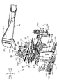
- FIG. 2 is a perspective view of the internal structure of the apparatus main body of the present embodiment as viewed diagonally from the front left.
- FIG. 3 is an exploded perspective view showing the internal structure and the mounting band of the apparatus main body of the present embodiment.
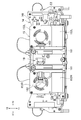
- FIG. 4 is a top view of the internal structure of the apparatus main body of the present embodiment as viewed from above.
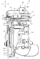
- FIG. 5 is a side view of the internal structure of the apparatus main body of the present embodiment as viewed from the left.
- FIG. 6 is a front view of the internal structure of the apparatus main body of the present embodiment as viewed from the front.
- the apparatus main body 10 includes a main frame 11, a right optical unit 12R, a left optical unit 12L, a camera unit 13, a circuit board 14, a cooling device 15, and a supported portion 16.
- a circuit board 14 is provided on the main frame 11, a cooling device 15 is provided on the circuit board 14, and a supported portion is provided on the cooling device 15. 16 is provided.
- the main frame 11 supports the right optical unit 12R, the left optical unit 12L, the camera unit 13, and the circuit board 14.
- the main frame 11 is preferably made of a lightweight and highly rigid material. For example, aluminum, magnesium, or the like may be used as the material of the main frame 11.
- the main frame 11 has a middle frame 111 extending in the vertical direction, an upper frame 112 connected to the upper part of the middle frame 111, and a lower frame 113 connected to the lower part of the middle frame 111.
- the middle frame 111 is provided substantially in the center of the apparatus main body 10.
- the width of the upper frame 112 and the lower frame 113 in the left-right direction is larger than the width of the middle frame 111 in the left-right direction. Therefore, as shown in FIG. 3 and the like, the main frame 11 has a shape in which the H shape is tilted 90 degrees laterally when viewed from the front-rear direction. That is, a space is formed between the right portion of the upper frame 112 and the right portion of the lower frame 113. Similarly, a space is formed between the left portion of the upper frame 112 and the left portion of the lower frame 113.
- the weight of the main frame 11 can be reduced as compared with the case where the shape (outer shape) when viewed from the front-rear direction is rectangular.
- the right optical unit 12R and the left optical unit 12L are arranged in a region formed between the middle frame 111 and the upper frame 112, and are supported by the middle frame 111, the upper frame 112, and the lower frame 113. ing.
- the right optical unit 12R has at least a lens (not shown) that guides the image light from the display device 110 to the user's right eye.
- the left optical unit 12L has at least a lens (not shown) that guides the image light from the display device 110 to the user's left eye.
- the display device 110 shown in FIG. 1 may be arranged in front of the lens included in the right optical unit 12R and the left optical unit 12L, respectively.
- the display device 110 may have a see-through type screen or may have a non-see-through type screen.
- the optical units 12R and 12L may have a nose pad or the like that comes into contact with the user's nose.
- the right optical unit 12R and the left optical unit 12L are supported by the main frame 11 so as to be movable left and right. Thereby, the user can adjust the distance between the lens included in the right optical unit 12R and the lens included in the left optical unit 12L in the left-right direction according to the distance between his / her left and right eyes. Further, as described above, in the main frame 11, a space is formed between the right portion of the upper frame 112 and the right portion of the lower frame 113, and the left portion of the upper frame 112 and the lower frame 113 A space is also formed between it and the left part.
- the configuration shown in the figure is an example, and the lens and the like are not limited to those that are unitized, and at least those that are built in the device main body 10 may be used.
- the camera unit 13 has at least a camera frame 131 and cameras 132 and 133 supported by the camera frame 131.
- the camera frame 131 is supported by the front portion of the middle frame 111.
- the cameras 132 and 133 are provided with an image sensor such as a CCD (Charge Coupled Device) or a CMOS (Complementary Metal Oxide Semiconductor), and image the front of the user wearing the HMD1.
- CCD Charge Coupled Device
- CMOS Complementary Metal Oxide Semiconductor
- a plurality of cameras 132 and 133 are provided, and for example, those used for SLAM (Simultaneous localization and mapping) that enable three-dimensional recognition by estimating the position and orientation of the camera from a captured image may be included. .. FIG. 2 and the like show a configuration in which four cameras are supported by the camera frame 131. However, the number and position of cameras are not limited to those shown in the figure. Although not shown, the housing 120 may have an opening so that the cameras 132 and 133 are exposed to each other.
- SLAM Simultaneous localization and mapping
- the circuit board 14 is supported by the upper frame 112.
- the size of the upper frame 112 may be larger than or substantially the same as the size of the circuit board 14. That is, the upper frame 112 may be a frame having a predetermined width in the front-rear direction and the left-right direction. As shown in FIG. 3 and the like, the upper frame 112 is connected to the upper part of the middle frame 111 so as to project rearward from the middle frame 111.
- the circuit board 14 mounts at least one or more electronic components.
- the surface of the circuit board 14 on which the integrated circuit 140 described later is mounted is referred to as a mounting surface 141.
- the circuit board 14 is supported by the upper frame 112 so that the mounting surface 141 faces upward when the HMD1 is in use.
- the apparatus main body 10 has a supported portion 16 on the upper portion thereof.
- the supported portion 16 is arranged above the cooling device 15.
- the supported portion 16 has a rail 161, an operation portion 162, and an operation assist portion 163.
- the rail 161 is provided so as to extend in the front-rear direction.
- the operation unit 162 is arranged on the right side of the rail 161 and projects upward.
- the operation assisting unit 163 is arranged on the left side of the rail 161 and projects upward.
- at least the rail 161 of the supported portion 16 is between the cooling fan 153R and the cooling fan 153L so as not to overlap the cooling fan 153R and the cooling fan 153L in the top view. It should be arranged.
- the support portion 212 of the front member 21 is fitted to the rail 161 so as to be slidable in the front-rear direction.
- the support portion 212 can move back and forth relative to the supported portion 16. That is, the device main body 10 can move back and forth relative to the mounting band 20. Therefore, the user can adjust the position of the apparatus main body 10 in the front-rear direction while the HMD1 is attached to the head H. As a result, the user can adjust the distance (also referred to as eye relief) between his / her own eye and the lens provided on the optical units 12R and 12L.
- the relative movement of the support portion 212 and the supported portion 16 is regulated by a regulation mechanism (not shown). Then, it is preferable that the user can switch from the state in which the relative movement between the support portion 212 and the supported portion 16 is restricted to the allowable state by operating the operation unit 162. For example, the user may push the operation unit 162 to the left (see the direction of the arrow in FIG. 6) to release the regulation by the regulation mechanism.
- the support portion 212 and the supported portion 16 can be relatively moved by the rack and pinion mechanism, and the regulation mechanism meshes with the rack gear or the pinion gear. , It is good that it is a mechanism that regulates their operation. Then, the operation unit 162 may release the engagement of the regulation mechanism with the rack gear or the pinion gear by operating the regulation mechanism. Further, the operation unit 162 may be configured to move to the original position (position shown in FIG. 3 or the like) by the elastic force of an elastic member such as a spring after receiving an operation from the user.
- the device main body 10 may have an operation assisting unit 163 so that the user can easily operate the operation unit 162.
- the user can easily push the operation unit 162 to the left by, for example, pinching the operation unit 162 and the operation assistance unit 163 with the index finger and the thumb.
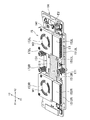
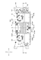
- FIG. 7 is a perspective view showing the cooling device and the circuit board of the present embodiment.
- FIG. 8 is a top view showing the cooling device and the circuit board of the present embodiment.
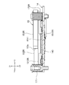
- FIG. 9 is a cross-sectional view showing a cross section cut along the IX-IX cutting line of FIG.
- FIG. 10 is a cross-sectional view showing a cross section cut along the XX cutting line of FIG.
- FIG. 11 is a front view schematically showing the vapor chamber and the electronic components mounted on the circuit board in this embodiment.
- FIG. 12 is an exploded perspective view showing the cooling device of the present embodiment.
- the cooling device 15 has a vapor chamber 151 which is a heat diffusion member, a right heat sink 152R, a left heat sink 152L, a right cooling fan 153R, and a left cooling fan 153L.
- the cooling device 15 is arranged so as to face the mounting surface 141 of the circuit board 14. More specifically, the vapor chamber 151 is arranged to face the mounting surface 141.
- the vapor chamber 151 includes a right mounting portion 1512R on which the right heat sink 152R and the right cooling fan 153R are mounted, and a left mounting portion 1512L on which the left heat sink 152L and the left cooling fan 153L are mounted. have.
- the vapor chamber 151 has a recessed portion (contact portion) 1511 provided between the right mounting portion 1512R and the left mounting portion 1512L.
- the vapor chamber 151 has a right connecting portion 1513R for connecting the right mounting portion 1512R and the recessed portion 1511, and a left connecting portion 1513L for connecting the left mounting portion 1512L and the recessed portion 1511.
- the right connecting portion 1513R is bent so as to be located upward from the recessed portion 1511 side toward the right mounting portion 1512R side. Therefore, the right mounting portion 1512R is located above the recessed portion 1511, and a gap is formed directly below the right connecting portion 1513R.
- the left connecting portion 1513L is bent so as to be located upward from the recessed portion 1511 side toward the left mounting portion 1512L side. Therefore, the left mounting portion 1512L is located above the recessed portion 1511, and a gap is formed directly below the left connecting portion 1513L.
- the vapor chamber 151 is filled with a fluid.
- the region of the vapor chamber 151 in which the fluid is sealed is defined as the heat diffusion region D.
- the region corresponding to the heat diffusion region D is shown by hatching.
- the heat diffusion region D is provided so as to straddle the right mounting portion 1512R, the right connecting portion 1513R, the recessed portion 1511, the left connecting portion 1513L, and the left mounting portion 1512L.
- the region directly below the heat sinks 152R and 152L is also a heat diffusion region D.
- the fluid sealed inside the vapor chamber 151 evaporates as the temperature rises, and heads toward the upper part inside the vapor chamber 151. As the fluid moves upward, heat is dissipated in the right heat sink 152R and the left heat sink 152L placed on the vapor chamber 151. The fluid is then condensed and the condensed fluid is circulated to the bottom of the vapor chamber 151.
- the right heat sink 152R and the left heat sink 152L are provided with a plurality of heat radiation fins extending upward from the circuit board 14 side. That is, the right heat sink 152R and the left heat sink 152L are configured to release the heat generated in the circuit board 14 upward.
- the recess portion 1511 is provided so that the lower surface thereof directly contacts the upper surface of the integrated circuit (IC) 140 mounted on the circuit board 14.
- the heat generated in the integrated circuit 140 is sent to the heat sinks 152R and 152L through the heat diffusion region D.
- the integrated circuit 140 may be, for example, a CPU (Central Processing Unit) that controls the entire HMD1.
- the present invention is not limited to this, and the integrated circuit 140 may be any circuit that consumes power as it is driven and can be a heat source.
- the integrated circuit 140 as the number and performance of the functions of the HMD1 are improved, the information processing becomes complicated and the power consumption increases. The larger the power consumption of the integrated circuit 140, the more heat is generated.
- the circuit board 14 mounts a plurality of electronic components.
- the thickness (height) of a plurality of electronic components varies.
- a gap sufficient for mounting electronic components is required between the cooling device 15 and the circuit board 14.
- the recessed portion 1511 of the vapor chamber 151 is in direct contact with the integrated circuit 140 as described above in order to enhance the heat dissipation effect. That is, the length between the lower surface of the recessed portion 1511 and the mounting surface 141 of the circuit board 14 substantially corresponds to the thickness of the integrated circuit 140.
- an electronic component E1 thicker than the integrated circuit 140 was arranged directly below the right mounting portion 1512R on the mounting surface 141.
- an electronic component E1 thicker than the integrated circuit 140 is arranged directly below the left mounting portion 1512L.
- the electronic component E1 may be arranged so that its upper surface is in contact with the lower surface of the right mounting portion 1512R or the left mounting portion 1512L. In this case, the heat generated from the electronic component E1 can be efficiently released.
- the electronic component E2 (second electronic component), which is thicker than the electronic component arranged directly under the right mounting portion 1512R and the left mounting portion 1512L, is as shown in FIGS. 7 and 11.
- the relatively thick connector may be arranged in a region of the mounting surface 141 that does not overlap with the cooling device 15 in the top view.
- the region of the mounting surface 141 that does not overlap with the cooling device 15 in the top view is the right portion or the left portion of the mounting surface 141.
- the electronic component E2 may be, for example, a connector to which various electrical wirings are connected.
- FIG. 11 for simplification, only one electronic component E1 is arranged directly under the right mounting portion 1512R and directly below the left mounting portion 1512L, but a plurality of electronic components E1 are arranged. It is good to have. Further, although only one electronic component E2 is shown in FIG. 11, it is preferable that a plurality of electronic components E2 are also arranged.
- the vapor chamber 151 is held in a state of being urged with respect to the circuit board 14 by the elastic force of the fixtures 171, 172R, and 172L having springs. Specifically, the fixtures 171 and 172R and 172L are inserted into the held holes 151h1, 151h2 and 151h3 shown in FIG. 12, respectively, and the holding holes 151h1 and 151h2 are provided by the springs included in the fixtures 171, 172R and 172L. , 151h3 may be pressed downward. With such a configuration, the recessed portion 1511 of the vapor chamber 151 elastically contacts the integrated circuit 140 mounted on the circuit board 14. Therefore, the contact state between the recessed portion 1511 and the integrated circuit 140 is stable, and the heat generated in the integrated circuit 140 can be more effectively transferred to the vapor chamber 151.
- the fixtures 171 and 172R and 172L are held between the circuit board 14 and the supported portion 16. That is, as shown in FIG. 6, the fixtures 171 and 172R and 172L may have a function of supporting the supported portion 161. Further, as shown in FIG. 6, the fixtures 171, 172R, and 172L may be arranged between the cooling fan 153R and the cooling fan 153L in the left-right direction. As a result, the circuit board 14 and the cooling device 15 can be arranged on the upper part of the apparatus main body 10, and the supported portion 161 can be arranged on the upper part and the center of the apparatus main body 10.
- the heat from the integrated circuit 140 can be efficiently released, and a plurality of electronic components can be mounted on the circuit board 14 without increasing the mounting surface 141 of the circuit board 14. It is possible to implement it in.
- the right heat sink 152R and the right cooling fan 153R are mounted on the right mounting portion 1512R of the vapor chamber 151.
- the right heat sink 152R and the right cooling fan 153R are provided adjacent to each other in the front-rear direction.
- the left heat sink 152L and the left cooling fan 153L are mounted on the left mounting portion 1512L of the vapor chamber 151.
- the left heat sink 152L and the left cooling fan 153L are provided adjacent to each other in the front-rear direction.
- the right cooling fan 153R has a blade W1 that rotates about a central axis OR (see FIGS. 8 and 9) extending in a direction extending through the circuit board 14.
- the left cooling fan 153L has blades W2 that rotate about a central axis OL (see FIGS. 8 and 9) extending in a direction penetrating the circuit board 14.
- the housing of the right cooling fan 153R is formed with an air outlet 153a that opens facing the right heat sink 152R.
- the housing of the left cooling fan 153L is also formed with an air outlet 153b that opens facing the left heat sink 152L.
- the blade W1 of the right cooling fan 153R is rotationally driven to generate cooling air sent toward the heat sink 152R through the air outlet 153a.
- cooling air sent toward the heat sink 152L through the air outlet 153b is generated.
- the direction of the cooling air generated by the cooling fans 153R and 153L is not limited to that described here.
- the cooling fans 153R and 153L may blow cooling air toward the circuit board 14.
- the air trapped below the cooling fans 153R and 152L may be sucked in and sent upward.
- the configuration shown in the present embodiment is effective for HMD1 which consumes a large amount of power in electronic components by improving the number of functions and performance. Specifically, for example, it is effective for HMD1 that employs a wireless communication technology that consumes a large amount of power.
- the circuit board 14 and the cooling device 15 having a certain weight are arranged at the front portion of the device main body 10 which is a position far from the head H of the user who wears the HMD 1, the center of gravity of the device main body 10 Will be located in front.
- the camera is further forward than them.
- the unit 13 will be arranged.
- the load applied to the user wearing the HMD1 increases, and the HMD1 tends to slip off from the user's head H. Therefore, it is necessary to take measures such as firmly fixing the wearing band 20 to the user's head H so that the HMD 1 does not slip off.
- the HMD1 of the present embodiment since the circuit board 14 and the cooling device 15 are arranged in the upper part of the apparatus main body 10, the HMD1 is compared with the configuration in which they are arranged in the front part of the apparatus main body 10. The load applied to the wearing user can be suppressed, and the HMD1 can be prevented from easily slipping off from the user's head H.
- the configuration of the HMD 1 described in the above embodiment is an example, and at least the circuit board 14 and the cooling device 15 may be arranged on the upper part of the apparatus main body 10.
- the configurations of the optical units 12R and 12L and the main frame 11 are not limited to those shown in the drawings.
- the cooling device 15 has the vapor chamber 151, the heat sinks 152R and 152L, and the cooling fans 153R and 153L has been described, but the present invention is not limited to this, and it occurs at least in the circuit board 14. Anything that has a cooling effect on the heat generated may be used. That is, the cooling device 15 may have only one of the vapor chamber, the heat sink, and the cooling fan, or may have other cooling structures. As another cooling structure, for example, a structure having a heat pipe may be used.
- cooling device 15 has two heat sinks and two cooling fans
- the present invention is not limited to this.
- support portions 212 may be formed on the right portion and the left portion, respectively, and one heat sink and one cooling fan may be provided between the two support portions 212.
- the mounting band 20 includes the front member 21 and is connected to the device main body 10 via the front member 21, but the present invention is not limited to this.
- the band portion of the mounting band 20 extending rearward may be directly connected to the device main body 10.
- HMD head-mounted display
Landscapes
- Physics & Mathematics (AREA)
- Engineering & Computer Science (AREA)
- General Physics & Mathematics (AREA)
- Theoretical Computer Science (AREA)
- Optics & Photonics (AREA)
- Computer Hardware Design (AREA)
- Human Computer Interaction (AREA)
- General Engineering & Computer Science (AREA)
- Devices For Indicating Variable Information By Combining Individual Elements (AREA)
- Cooling Or The Like Of Electrical Apparatus (AREA)
Abstract
ヘッドマウントディスプレイ(1)は、装置本体(10)と、装置本体(10)を支持すると共に、ユーザの頭部(H)に装着される装着バンド(20)と、装置本体(10)の上部に配置されており、1以上の電子部品を実装する実装面(141)を有する回路基板14と、装置本体(10)の上部において実装面(141)に対向して配置される冷却装置(15)と、を有する。
Description
本発明は、ヘッドマウントディスプレイに関する。
ユーザの頭部に装着して利用するヘッドマウントディスプレイの開発が進められている。特許文献1に開示されるように、ヘッドマウントディスプレイは、ディスプレイが内蔵される装置本体と、装置本体を支持すると共に、ユーザの頭部を囲むバンドとを備えている。
ここで、ヘッドマウントディスプレイにおいては、機能の数や性能を向上させると共に、消費電力が増加することとなる。消費電力が増加すると、ヘッドマウントディスプレイの各種機能を制御する電子部品の温度が上昇しやすくなる。電子部品の温度が過度に上昇してしまうと、誤動作が生じたり、動作が停止したりしてしまう可能性がある。特許文献1には、電子部品の温度の上昇を抑制するためにヒートパイプやファンを備えたヘッドマウントディスプレイが開示されている。しかしながら、特許文献1に開示されるようにヘッドマウントディスプレイの装置本体の前部に冷却機器を設ける構成においては、装置本体の重心が前方に位置することとなり、ヘッドマウントディスプレイを装着するユーザにかかる負荷が大きくなってしまう。
本明細書の目的の一つは、電子部品の温度が過度に上昇することを抑制すると共に、ユーザにかかる負荷を低減するヘッドマウントディスプレイを提供することにある。
本開示で提案するヘッドマウントディスプレイの一例は、装置本体と、前記装置本体を支持すると共に、ユーザの頭部に装着される装着バンドと、前記装置本体の上部に配置されており、1以上の電子部品を実装する実装面を有する回路基板と、前記装置本体の上部において前記実装面に対向して配置される冷却装置と、を有する。
上記のヘッドマウントディスプレイによると、電子部品の温度が過度に上昇することを抑制すると共に、ユーザにかかる負荷を低減することができる。
以下、図面を参照して、本発明の実施形態について説明する。以下の説明では、図中のX1及びX2が示す方向をそれぞれ右方及び左方とし、図中のY1及びY2が示す方向をそれぞれ前方及び後方とし、図中のZ1及びZ2が示す方向をそれぞれ上方及び下方とする。これら各方向は、ヘッドマウントディスプレイ1を装着したユーザから見た方向を示している。また、以下の説明では、ヘッドマウントディスプレイ1をHMD(Head Mounted Display)1と称する。
[HMD1の全体構成の概要]
図1に示すように、HMD1は、装置本体10と、装着バンド20とを有している。
図1に示すように、HMD1は、装置本体10と、装着バンド20とを有している。
装置本体10は、図1に示すように、少なくとも、表示装置110と、表示装置110を収容すると共に、装置本体10の外観を構成するハウジング120とを有している。表示装置110は、例えば、液晶表示装置や有機エレクトロルミネセンス表示装置であるとよいが、その種類は特に限定されない。HMD1の使用時、装置本体10はユーザの眼前を覆う。
装着バンド20は、装置本体10から後方に延びている。HMD1の使用時、装着バンド20はユーザの頭部Hを取り囲む。装着バンド20は、環状であり、その内側に頭部Hが配置されるとよい。HMD1の例では、装着バンド20は、後方且つ下方に斜めに延びている。ただし、これに限られるものではなく、装着バンド20は水平に延びていてもよい。
HMD1の例では、装着バンド20は、その前部にフロント部材21を有している。フロント部材21は、額当て部211と、支持部212とを有している。
HMD1の使用時、フロント部材21の額当て部211はユーザの頭部Hの前面に当てられる。額当て部211の内面(後面)にはクッションが設けられてもよい。また、額当て部211の内面(後面)は、頭部Hの前面にフィットするように湾曲してもよい。
支持部212は、額当て部211の下部から前方に伸びている。支持部212は、装置本体10の上部に設けられる被支持部16を支持している。これにより、装置本体10は、装着バンド20に支持されて、装着バンド20を装着したユーザの眼前に配置されることとなる。
[装置本体100の内部構造]
さらに、図2~図6を参照して、本実施形態に係るHMD1における装置本体10の内部構造の詳細について説明する。なお、本実施形態においては、装置本体10の内部構造とは、装置本体10のうち、図1に示すハウジング12を除いた部分である。
さらに、図2~図6を参照して、本実施形態に係るHMD1における装置本体10の内部構造の詳細について説明する。なお、本実施形態においては、装置本体10の内部構造とは、装置本体10のうち、図1に示すハウジング12を除いた部分である。
図2は、本実施形態の装置本体の内部構造を左斜め前から見た斜視図である。図3は、本実施形態の装置本体の内部構造及び装着バンドを示す分解斜視図である。図4は、本実施形態の装置本体の内部構造を上方から見た上面図である。図5は、本実施形態の装置本体の内部構造を左方から見た側面図である。図6は、本実施形態の装置本体の内部構造を前方から見た前面図である。
装置本体10は、図3に示すように、メインフレーム11と、右光学ユニット12Rと、左光学ユニット12Lと、カメラユニット13と、回路基板14と、冷却装置15と、被支持部16とを有している。図3に示すように、HMD1においては、メインフレーム11上には回路基板14が設けられており、回路基板14上には冷却装置15が設けられており、冷却装置15上には被支持部16が設けられている。
メインフレーム11は、右光学ユニット12R、左光学ユニット12L、カメラユニット13、回路基板14を支持している。メインフレーム11は、軽量かつ剛性の高い材料からなるとよい。例えば、メインフレーム11の材料としてはアルミニウムやマグネシウム等を採用するとよい。
メインフレーム11は、上下方向に延伸する中フレーム111と、中フレーム111の上部に接続される上フレーム112と、中フレーム111の下部に接続される下フレーム113とを有している。
中フレーム111は、装置本体10の略中央に設けられている。上フレーム112及び下フレーム113の左右方向の幅は、中フレーム111の左右方向の幅よりも大きい。そのため、図3等に示すように、メインフレーム11は、前後方向から見た場合に、H形状が90度横に傾いたような形状となっている。すなわち、上フレーム112の右部と、下フレーム113の右部との間に空間が形成されている。同様に、上フレーム112の左部と、下フレーム113の左部との間にも空間が形成されている。このような形状としたことにより、前後方向から見た場合の形状(外形)を矩形とした場合と比較して、メインフレーム11を軽量化することができる。
また、右光学ユニット12R及び左光学ユニット12Lは、中フレーム111と上フレーム112との間に形成される領域に配置されており、中フレーム111、上フレーム112、及び下フレーム113とによって支持されている。
右光学ユニット12Rは、表示装置110からの画像光を、ユーザの右眼に導くレンズ(不図示)を少なくとも有している。同様に、左光学ユニット12Lは、表示装置110からの画像光を、ユーザの左眼に導くレンズ(不図示)を少なくとも有している。また、図1に示した表示装置110は、右光学ユニット12R及び左光学ユニット12Lが有するレンズの前方にそれぞれ配置されているとよい。表示装置110は、シースルー型の画面を有するものであってもよいし、非シースルー型の画面を有するものであってもよい。また、光学ユニット12R、12Lは、ユーザの鼻に接触する鼻パッドなどを有していてもよい。
また、右光学ユニット12Rと左光学ユニット12Lは、左右に移動可能にメインフレーム11に支持されているとよい。これにより、ユーザは、左右方向における、右光学ユニット12Rが備えるレンズと左光学ユニット12Lが備えるレンズとの間隔を、自己の左右の眼の間隔に応じて、調整することができる。また、上述のように、メインフレーム11においては、上フレーム112の右部と、下フレーム113の右部との間に空間が形成されており、上フレーム112の左部と、下フレーム113の左部との間にも空間が形成されている。すなわち、メインフレーム11の右部及び左部において、右光学ユニット12R及び左光学ユニット12Lの左右方向における移動を規制する部分が存在しない。そのため、右光学ユニット12R及び左光学ユニット12Lの左右方向における可動範囲を十分にとることができる。
なお、図示の構成は一例であり、レンズ等はユニット化されているものに限られるものではなく、少なくとも、装置本体10に内蔵されるものであればよい。
カメラユニット13は、少なくとも、カメラフレーム131と、カメラフレーム131に支持されるカメラ132、133を有している。カメラフレーム131は、中フレーム111の前部に支持されている。カメラ132、133は、例えば、CCD(Charge Coupled Device)またはCMOS(Complementary Metal Oxide Semiconductor)等の撮像素子を備えており、HMD1を装着したユーザの前方を撮像する。
カメラ132、133は、複数設けられており、例えば、撮影画像からカメラの位置や姿勢を推定することにより3次元認識を可能にするSLAM(Simultaneous localization and mapping)用に用いられるものを含むとよい。図2等においては、4つのカメラがカメラフレーム131に支持される構成を示している。ただし、カメラの個数や位置は図示するものに限られるものではない。なお、図示は省略するが、ハウジング120は、カメラ132、133がそれぞれ露出するように開口を有しているとよい。
回路基板14は、上フレーム112に支持されている。上面視において、上フレーム112の大きさは、回路基板14の大きさよりも大きい又は略同じであるとよい。すなわち、上フレーム112は、前後方向及び左右方向において所定の幅を有するフレームであるとよい。上フレーム112は、図3等に示すように、中フレーム111から後方に突出するように、中フレーム111の上部に接続されている。
回路基板14は、少なくとも1以上の電子部品を実装している。以下、回路基板14のうち後述の集積回路140を実装する側の面を実装面141と呼ぶ。本実施形態においては、回路基板14は、HMD1の使用状態において、実装面141が上方を向くように、上フレーム112に支持されている。
また、図1でも示したように、装置本体10は、その上部に被支持部16を有している。被支持部16は、冷却装置15の上方に配置されている。
被支持部16は、図3、図4等に示すように、レール161と、操作部162と、操作補助部163とを有している。レール161は、前後方向に延伸して設けられている。操作部162は、レール161の右側に配置されており、上方に突出している。操作補助部163は、レール161の左側に配置されており、上方に突出している。なお、図6に示すように、被支持部16のうち少なくともレール161は、上面視において、冷却ファン153Rと冷却ファン153Lとの間であって、冷却ファン153Rと冷却ファン153Lと重ならないように配置されているとよい。
フロント部材21の支持部212は、前後方向にスライド可能にレール161に嵌められる。支持部212は、被支持部16に対して相対的に前後動可能となっている。すなわち、装置本体10は、装着バンド20に対して相対的に前後動可能となっている。そのため、ユーザは、HMD1を頭部Hに装着した状態で、装置本体10の前後方向における位置を調整することができる。これにより、ユーザは、自己の眼と、光学ユニット12R、12Lに設けられるレンズとの距離(アイレリーフとも呼ばれる)を調整することができる。
また、支持部212と被支持部16とは、不図示の規制機構により、相対移動が規制されているとよい。そして、ユーザが、操作部162を操作することにより、支持部212と被支持部16との相対移動が規制された状態から、許容される状態に切り替え可能であるとよい。例えば、ユーザが、操作部162を左方に押すことにより(図6の矢印方向参照)、規制機構による規制が解除されるとよい。
なお、規制機構の説明の詳細については省略するが、例えば、支持部212と被支持部16とがラックピニオン機構により相対移動可能となっており、規制機構は、ラックギア又はピニオンギアに噛み合うことにより、それらの動作を規制する機構であるとよい。そして、操作部162は、規制機構を動作させることにより、ラックギア又はピニオンギアに対する規制機構の噛み合いを解除するものであるとよい。また、操作部162は、ユーザからの操作を受け付けた後、バネ等の弾性部材の弾性力により、元の位置(図3等に示す位置)に移動するように構成されているとよい。
また、装置本体10は、ユーザが操作部162を操作しやすいように、操作補助部163を有するとよい。ユーザは、例えば、操作部162と操作補助部163とを人差し指と親指とで摘むことにより、操作部162を左方向に容易に押すことができる。
さらに、図7~図12を参照して、本実施形態の冷却装置15の詳細について説明する。図7は、本実施形態の冷却装置及び回路基板を示す斜視図である。図8は、本実施形態の冷却装置及び回路基板を示す上面図である。図9は、図8のIX-IX切断線で切断した断面を示す断面図である。図10は、図8のX-X切断線で切断した断面を示す断面図である。図11は、本実施形態におけるベイパーチャンバと回路基板に実装される電子部品とを模式的に示す前面図である。図12は、本実施形態の冷却装置を示す分解斜視図である。
冷却装置15は、熱拡散部材であるベイパーチャンバ151と、右ヒートシンク152Rと、左ヒートシンク152Lと、右冷却ファン153Rと、左冷却ファン153Lとを有している。
冷却装置15は、回路基板14の実装面141に対向して配置されている。より具体的には、ベイパーチャンバ151が実装面141に対向して配置されている。
ベイパーチャンバ151は、図12等に示すように、右ヒートシンク152Rと右冷却ファン153Rを載置する右載置部1512Rと、左ヒートシンク152Lと左冷却ファン153Lを載置する左載置部1512Lとを有している。
また、ベイパーチャンバ151は、右載置部1512Rと左載置部1512Lとの間に設けられる窪み部(接触部)1511を有している。
また、ベイパーチャンバ151は、右載置部1512Rと窪み部1511とを接続する右接続部1513Rと、左載置部1512Lと窪み部1511とを接続する左接続部1513Lとを有している。
図11に示すように、右接続部1513Rは、窪み部1511側から右載置部1512R側に向かうに従い上方に位置するように屈曲している。そのため、右載置部1512Rは、窪み部1511よりも上方に位置しており、右接続部1513Rの直下には隙間が形成されている。
同様に、左接続部1513Lは、窪み部1511側から左載置部1512L側に向かうに従い上方に位置するように屈曲している。そのため、左載置部1512Lは、窪み部1511よりも上方に位置しており、左接続部1513Lの直下には隙間が形成されている。
ベイパーチャンバ151は、その内部に流体が封入されている。以下の説明において、ベイパーチャンバ151のうち内部に流体が封入されている領域を熱拡散領域Dと定義する。なお、図7、図8、図12において、熱拡散領域Dに対応する領域を、ハッチングを施すことにより示している。図12に示すように、熱拡散領域Dは、右載置部1512R、右接続部1513R、窪み部1511、左接続部1513L、左載置部1512Lを跨って設けられている。なお、図面には表れていないが、ヒートシンク152R、152Lの直下の領域も熱拡散領域Dとなっている。
ベイパーチャンバ151の内部に封入される流体は、温度が上昇することにより蒸発し、ベイパーチャンバ151内の上部に向かう。流体が上部に向かうことにより、ベイパーチャンバ151上に載置される右ヒートシンク152R及び左ヒートシンク152Lにおいて放熱が行われる。その後、流体は凝縮し、凝縮した流体は、ベイパーチャンバ151の下部へ環流される。
右ヒートシンク152R及び左ヒートシンク152Lは、回路基板14側から上方に向けて延伸する放熱フィンを複数備えている。すなわち、右ヒートシンク152R及び左ヒートシンク152Lは、回路基板14で発生した熱を、上方に放出する構成となっている。
本実施形態において、図11に示すように、窪み部1511は、その下面が回路基板14に実装される集積回路(IC:integrated circuit)140の上面に直接接触するように設けられている。このような構成により、集積回路140で発生した熱を、熱拡散領域Dを通じて、ヒートシンク152R、152Lへ送っている。
なお、集積回路140は、例えば、HMD1の全体を制御するCPU(Central Processing Unit)であるとよい。ただし、これに限られるものではなく、集積回路140は、その駆動に伴い電力消費が行われ、熱源となり得る回路であればよい。集積回路140においては、HMD1の機能の数や性能が向上するほど、その情報処理が煩雑となり、消費電力が大きくなる。集積回路140は、消費電力が大きいほど熱を生じることとなる。
ここで、回路基板14は、複数の電子部品を実装している。複数の電子部品の厚さ(高さ)は様々である。冷却装置15と回路基板14との間には、電子部品を実装できる程度の隙間が必要となる。ベイパーチャンバ151の窪み部1511は、放熱効果を高めるため、上述のように、集積回路140に直接的に接触している。すなわち、窪み部1511の下面と、回路基板14の実装面141との間の長さは、集積回路140の厚さに略対応している。
そのため、集積回路140よりも厚さの厚い電子部品については、窪み部1511の下面と、回路基板14の実装面141との間に配置することができない。そこで、本実施形態においては、上述のように、右載置部1512R及び左載置部1512Lを、窪み部1511よりも上方に配置することにより、右載置部1512R及び左載置部1512Lの直下に空間が形成される構成を採用した。すなわち、右載置部1512R及び左載置部1512Lと回路基板14の実装面141との間の隙間を、窪み部1511と回路基板14の実装面141との間の隙間よりも広くした。
そして、図11に示すように、実装面141のうち、右載置部1512Rの直下に、集積回路140よりも厚さの厚い電子部品E1(第1の電子部品)を配置した。同様に、実装面141のうち、左載置部1512Lの直下に、集積回路140よりも厚さの厚い電子部品E1(第1の電子部品)を配置した。なお、電子部品E1は、その上面が、右載置部1512R又は左載置部1512Lの下面に接触するように配置されていてもよい。この場合、電子部品E1から生じる熱を効率的に放出することができる。一方、電子部品E1の上面を右載置部1512R又は左載置部1512Lの下面に非接触とした場合、集積回路140からのみベイパーチャンバ151に熱が直接伝わるため、集積回路140から発生した熱をより効果的に放出することが可能となる。
さらに、右載置部1512Rや左載置部1512Lの直下に配置される電子部品よりも、さらに厚さの厚い電子部品E2(第2の電子部品)については、図7、図11に示すように、上面視において実装面141のうち冷却装置15と重ならない領域に配置した。すなわち、回路基板14に実装される電子回路のうち、比較的厚さの厚いコネクタは、上面視において実装面141のうち冷却装置15と重ならない領域に配置されるとよい。なお、本実施形態においては、上面視において実装面141のうち冷却装置15と重ならない領域とは、実装面141の右部又は左部である。なお、電子部品E2は、例えば、種々の電気配線が接続されるコネクタであるとよい。
なお、図11においては、簡略化して、右載置部1512Rの直下及び左載置部1512Lの直下に配置される電子部品E1をそれぞれ1つのみ示しているが、電子部品E1は複数配置されているとよい。また、図11においては、電子部品E2を1つのみ示しているが、電子部品E2も複数配置されているとよい。
また、ベイパーチャンバ151は、スプリングを備える固定具171、172R、172Lの弾性力により、回路基板14に対して付勢された状態で保持されているとよい。具体的には、図12に示す被保持孔151h1、151h2、151h3のそれぞれに、固定具171、172R、172Lが挿通されて、固定具171、172R、172Lが備えるスプリングにより被保持孔151h1、151h2、151h3の周縁部が下方に押圧されているとよい。このような構成により、ベイパーチャンバ151の窪み部1511は、回路基板14に実装される集積回路140に対して弾性的に接触することとなる。そのため、窪み部1511と、集積回路140の接触状態は安定しており、集積回路140で発生した熱を、より効果的にベイパーチャンバ151へと伝達することができる。
固定具171、172R、172Lは、回路基板14と被支持部16との間で保持されているとよい。すなわち、図6に示すように、固定具171、172R、172Lは、被支持部161を支持する機能を有するものであるとよい。また、図6に示すように、固定具171、172R、172Lは、左右方向において、冷却ファン153Rと冷却ファン153Lとの間に配置されているとよい。これにより、回路基板14及び冷却装置15を装置本体10の上部に配置すると共に、被支持部161を装置本体10の上部かつ中央に配置する構成とすることができる。
ベイパーチャンバ151を以上説明したような構成にしたことにより、集積回路140からの熱を効率的に放出すると共に、回路基板14の実装面141を大きくすることなく、複数の電子部品を回路基板14に実装することが可能となる。
また、ベイパーチャンバ151の右載置部1512Rには、右ヒートシンク152Rと右冷却ファン153Rが載置されている。右ヒートシンク152Rと右冷却ファン153Rは、前後方向で互いに隣り合って設けられている。
同様に、ベイパーチャンバ151の左載置部1512Lには、左ヒートシンク152Lと左冷却ファン153Lが載置されている。左ヒートシンク152Lと左冷却ファン153Lは、前後方向で互いに隣り合って設けられている。
右冷却ファン153Rは、回路基板14を貫く方向に延伸する中心軸OR(図8、図9参照)を中心として回転する羽根W1を有している。同様に、左冷却ファン153Lは、回路基板14を貫く方向に延伸する中心軸OL(図8、図9参照)を中心として回転する羽根W2を有している。
また、図12に示すように、右冷却ファン153Rのハウジングには、右ヒートシンク152Rに対向して開口する送風口153aが形成されている。同様に、左冷却ファン153Lのハウジングにも、左ヒートシンク152Lに対向して開口する送風口153bが形成されている。
右冷却ファン153Rの羽根W1が回転駆動することにより、送風口153aを通じてヒートシンク152Rに向けて送られる冷却風が生じる。同様に、左冷却ファン153Lの羽根W2が回転駆動することにより、送風口153bを通じてヒートシンク152Lに向けて送られる冷却風が生じる。このような構成により、冷却装置15における冷却性能がより向上する。なお、冷却ファン153R、153Lが発生させる冷却風の送風向きは、ここで説明したものに限られない。例えば、冷却ファン153R、153Lは、回路基板14に向けて冷却風を送風するものであってもよい。または、冷却ファン153R、152Lの下方で籠もった空気を吸い込み、上方に送る構成であってもよい。
以上説明したHMD1においては、冷却装置15を有することにより、回路基板14が実装する電子部品から熱が発生した場合であっても、過度に温度が上昇することが抑制される。その結果、HMD1の誤動作や駆動の停止等を抑制することができる。特に、本実施形態で示した構成は、機能の数や性能を向上させることにより、電子部品における電力消費が大きなHMD1に有効である。具体的には、例えば、電力消費が大きい無線通信技術を採用するHMD1などに有効である。
ここで、ある程度の重量のある回路基板14及び冷却装置15が、HMD1を装着したユーザの頭部Hから遠い位置である、装置本体10の前部に配置されていると、装置本体10の重心が前方に位置することとなってしまう。特に、本実施形態で示したように、HMD1の前方を撮像するカメラを有する構成においては、回路基板14及び冷却装置15を装置本体10の前部に配置した場合、それらよりもさらに前方にカメラユニット13を配置することとなる。
その結果、HMD1を装着したユーザにかかる負荷が増加する共に、HMD1がユーザの頭部Hからずれ落ちやすくなってしまう。そのため、HMD1がずれ落ちないように、装着バンド20をユーザの頭部Hに強固に固定する等の対策を施す必要が生じてしまう。本実施形態のHMD1においては、回路基板14及び冷却装置15が、装置本体10の上部に配置されていることより、それらが装置本体10の前部に配置される構成と比較して、HMD1を装着したユーザにかかる負荷が抑制され、また、HMD1がユーザの頭部Hからずれ落ちやすくなってしまうことを抑制できる。
なお、上記実施形態で説明したHMD1の構成は一例であり、少なくとも、装置本体10の上部に回路基板14及び冷却装置15が配置されるものであればよい。例えば、光学ユニット12R、12Lや、メインフレーム11の構成等は、図示したものに限られるものではない。
また、本実施形態においては、冷却装置15が、ベイパーチャンバ151、ヒートシンク152R、152L、及び冷却ファン153R、153Lを有する例について説明したが、これに限られるものではなく、少なくとも回路基板14において発生する熱に対して冷却効果を有するものであればよい。すなわち、冷却装置15は、ベイパーチャンバ、ヒートシンク、冷却ファンのいずれか1つのみを有するものであってもよいし、その他の冷却構造を備えるものであってもよい。その他の冷却構造としては、例えば、ヒートパイプを有するものであってもよい。
また、本実施形態においては、冷却装置15が、ヒートシンク及び冷却ファンをそれぞれ2つ有する例について説明したが、これに限られるものではない。例えば、装着バンド20において、支持部212を右部と左部にそれぞれ形成し、それら2つの支持部212の間に1つのヒートシンク及び1つの冷却ファンを設けてもよい。
また、本実施形態においては、装着バンド20がフロント部材21を備えており、フロント部材21を介して装置本体10に接続される構成を示したが、これに限られるものではない。例えば、装着バンド20のうち後方に延びるバンド部分が装置本体10に直接接続される構成であっても構わない。
1 ヘッドマウントディスプレイ(HMD)、10 装置本体、14 回路基板、15 冷却装置、20 装着バンド。
Claims (20)
- 装置本体と、
前記装置本体を支持すると共に、ユーザの頭部に装着される装着バンドと、
前記装置本体の上部に配置されており、1以上の電子部品を実装する実装面を有する回路基板と、
前記装置本体の上部において前記実装面に対向して配置される冷却装置と、
を有するヘッドマウントディスプレイ。 - 前記装置本体は、表示装置を内蔵しており、
前記回路基板及び前記冷却装置は、前記表示装置より上方に配置されている、
請求項1に記載のヘッドマウントディスプレイ。 - 前記装置本体は、表示装置と、表示装置からの画像光をユーザの眼に導くレンズとを内蔵しており、
前記回路基板及び前記冷却装置は、前記レンズより上方に配置されている、
請求項1に記載のヘッドマウントディスプレイ。 - 前記回路基板は、前記実装面が上方を向くように配置されている、
請求項1~3のいずれか1項に記載のヘッドマウントディスプレイ。 - 前記装置本体は、前記装着バンドに支持される被支持部を有し、
前記被支持部は、少なくとも一部が前記冷却装置の上方に配置されている、
請求項1~4のいずれか1項に記載のヘッドマウントディスプレイ。 - 前記被支持部は、前記装着バンドに対して前後方向に相対的に移動可能に前記装着バンドに支持されている、
請求項5に記載のヘッドマウントディスプレイ。 - 少なくとも一部が前記冷却装置より上方に設けられており、ユーザからの操作を受け付けることにより、前記装着バンドに対する前記被支持部の相対的な移動の規制を解除する操作部を有する、
請求項6に記載のヘッドマウントディスプレイ。 - 前記冷却装置は、冷却風を生じさせる冷却ファンを含む、
請求項5~7のいずれか1項に記載のヘッドマウントディスプレイ。 - 前記冷却ファンは、前記被支持部の左右両側にそれぞれ配置されている、
請求項8に記載のヘッドマウントディスプレイ。 - 前記冷却ファンは、中心軸を中心として回転する羽根を有し、
前記中心軸の延伸方向は、前記回路基板を貫く方向である、
請求項8又は9に記載のヘッドマウントディスプレイ。 - 前記冷却装置は、放熱フィンを含む、
請求項1~10のいずれか1項に記載のヘッドマウントディスプレイ。 - 前記放熱フィンは、所定方向に並んで複数設けられており、前記回路基板が設けられる側から上方に向けて延伸している、
請求項11に記載のヘッドマウントディスプレイ。 - 前記回路基板は、前記電子部品として集積回路を実装しており、
前記冷却装置は、前記集積回路に接触すると共に前記集積回路から生じた熱を拡散させる熱拡散部材を含む、
請求項1~12のいずれか1項に記載のヘッドマウントディスプレイ。 - 前記熱拡散部材には、その内部に、温度に応じて蒸発又は凝縮する流体が封入されている、
請求項13に記載のヘッドマウントディスプレイ。 - 前記熱拡散部材は、少なくとも放熱フィンを載せる載置部を含む、
請求項13又は14に記載のヘッドマウントディスプレイ。 - 前記熱拡散部材は、前記載置部を、前記集積回路と接触する接触部よりも上方に配置するように、前記載置部と前記接触部とを接続する接続部とを含む、
請求項15に記載のヘッドマウントディスプレイ。 - 前記1以上の電子部品は、前記載置部の直下において前記実装面に実装されており、前記集積回路よりも厚みが厚い第1の電子部品を含む、
請求項15又は16に記載のヘッドマウントディスプレイ。 - 前記1以上の電子部品は、上面視において、前記冷却装置と重ならないように配置されており、前記第1の電子部品よりも厚みが厚い第2の電子部品を含む、
請求項17に記載のヘッドマウントディスプレイ。 - 前記集積回路に対して前記熱拡散部材を弾性的に接触させる弾性部材を有する、
請求項13~18のいずれか1項に記載のヘッドマウントディスプレイ。 - 前記装置本体は、その前部に、カメラと、該カメラを支持するフレームとを含むカメラユニットを有する、
請求項1~19のいずれか1項に記載のヘッドマウントディスプレイ。
Priority Applications (4)
| Application Number | Priority Date | Filing Date | Title |
|---|---|---|---|
| US17/435,872 US12117618B2 (en) | 2019-03-19 | 2019-03-19 | Head-mounted display |
| PCT/JP2019/011518 WO2020188760A1 (ja) | 2019-03-19 | 2019-03-19 | ヘッドマウントディスプレイ |
| JP2021506903A JP7279151B2 (ja) | 2019-03-19 | 2019-03-19 | ヘッドマウントディスプレイ |
| JP2023078015A JP7490112B2 (ja) | 2019-03-19 | 2023-05-10 | ヘッドマウントディスプレイ |
Applications Claiming Priority (1)
| Application Number | Priority Date | Filing Date | Title |
|---|---|---|---|
| PCT/JP2019/011518 WO2020188760A1 (ja) | 2019-03-19 | 2019-03-19 | ヘッドマウントディスプレイ |
Publications (1)
| Publication Number | Publication Date |
|---|---|
| WO2020188760A1 true WO2020188760A1 (ja) | 2020-09-24 |
Family
ID=72519756
Family Applications (1)
| Application Number | Title | Priority Date | Filing Date |
|---|---|---|---|
| PCT/JP2019/011518 Ceased WO2020188760A1 (ja) | 2019-03-19 | 2019-03-19 | ヘッドマウントディスプレイ |
Country Status (3)
| Country | Link |
|---|---|
| US (1) | US12117618B2 (ja) |
| JP (2) | JP7279151B2 (ja) |
| WO (1) | WO2020188760A1 (ja) |
Cited By (1)
| Publication number | Priority date | Publication date | Assignee | Title |
|---|---|---|---|---|
| JP2023049402A (ja) * | 2021-09-29 | 2023-04-10 | キヤノン株式会社 | 画像表示装置。 |
Families Citing this family (12)
| Publication number | Priority date | Publication date | Assignee | Title |
|---|---|---|---|---|
| US20230032004A1 (en) * | 2020-01-06 | 2023-02-02 | Lg Electronics Inc. | Display device |
| US11669127B2 (en) * | 2021-06-30 | 2023-06-06 | Meta Platforms Technologies, Llc | Extended reality headset positioning and stabilization |
| US11782281B2 (en) * | 2021-07-30 | 2023-10-10 | Meta Platforms Technologies, Llc | Thermal management system for electronic device |
| US12222515B2 (en) * | 2022-06-29 | 2025-02-11 | Meta Platforms Technologies, Llc | Apparatus, systems, and methods for heat transfer in optical devices |
| US20240012256A1 (en) * | 2022-07-07 | 2024-01-11 | Apple Inc. | Head-Mounted Display |
| EP4554348A4 (en) * | 2022-08-29 | 2025-11-05 | Samsung Electronics Co Ltd | ELECTRONIC DEVICE COMPRISING A HEAT PIPE SURROUNDING MULTIPLE INTEGRATED CIRCUITS |
| CN116381931A (zh) * | 2023-01-17 | 2023-07-04 | 富泰华工业(深圳)有限公司 | 头戴式设备 |
| WO2024232497A2 (ko) * | 2023-05-09 | 2024-11-14 | 삼성전자 주식회사 | 방열 구조를 포함하는 웨어러블 전자 장치 |
| EP4651653A4 (en) | 2023-05-09 | 2026-04-29 | Samsung Electronics Co Ltd | Wearable electronic device incorporating a heat dissipation structure |
| EP4711835A1 (en) * | 2023-05-12 | 2026-03-18 | Samsung Electronics Co., Ltd. | Heat dissipation member and wearable electronic device comprising heat dissipation member |
| CN120215113A (zh) * | 2023-12-26 | 2025-06-27 | 北京字跳网络技术有限公司 | 头戴显示设备 |
| WO2026058974A1 (ko) * | 2024-09-10 | 2026-03-19 | 엘지전자 주식회사 | 디스플레이 디바이스 및 이를 구비하는 전자 디바이스 |
Citations (6)
| Publication number | Priority date | Publication date | Assignee | Title |
|---|---|---|---|---|
| JPH0915527A (ja) * | 1995-06-27 | 1997-01-17 | Olympus Optical Co Ltd | 頭部装着型映像表示装置 |
| JPH11202795A (ja) * | 1998-01-09 | 1999-07-30 | Canon Inc | 映像表示装置 |
| JP2007012912A (ja) * | 2005-06-30 | 2007-01-18 | Polymatech Co Ltd | 熱伝導性部材および該熱伝導性部材を用いた冷却構造 |
| WO2015008326A1 (ja) * | 2013-07-16 | 2015-01-22 | 三協立山株式会社 | ヒートシンク及びヒートシンクの製造方法 |
| WO2015137165A1 (ja) * | 2014-03-14 | 2015-09-17 | 株式会社ソニー・コンピュータエンタテインメント | ヘッドマウントディスプレイ |
| US20170184863A1 (en) * | 2015-12-24 | 2017-06-29 | Sulon Technologies Inc. | Cooling system for head mounted device |
Family Cites Families (18)
| Publication number | Priority date | Publication date | Assignee | Title |
|---|---|---|---|---|
| JP2959000B2 (ja) | 1989-12-19 | 1999-10-06 | ソニー株式会社 | 顔面装着型視覚装置 |
| JPH0713100A (ja) | 1993-06-25 | 1995-01-17 | Olympus Optical Co Ltd | 頭部装着式ディスプレイ |
| JPH0934376A (ja) * | 1995-07-21 | 1997-02-07 | Olympus Optical Co Ltd | 頭部装着型映像表示装置 |
| JP2005296467A (ja) | 2004-04-14 | 2005-10-27 | Olympus Corp | 立体内視鏡用表示制御装置 |
| JP4528289B2 (ja) | 2006-07-31 | 2010-08-18 | オリンパス株式会社 | 頭部装着型映像表示装置 |
| JP2018101704A (ja) | 2016-12-20 | 2018-06-28 | キヤノン株式会社 | 電子機器 |
| CN106873165A (zh) | 2017-04-10 | 2017-06-20 | 北京小米移动软件有限公司 | 虚拟现实眼镜 |
| CN108700741B (zh) | 2017-04-14 | 2021-08-24 | 深圳市大疆创新科技有限公司 | 头戴设备及具有该头戴设备的视频眼镜 |
| US10379583B2 (en) * | 2017-04-19 | 2019-08-13 | Facebook Technologies, Llc | System for discharging heat out of head-mounted display based on hybrid fan and heat pipe |
| JP2018190825A (ja) | 2017-05-02 | 2018-11-29 | キヤノン株式会社 | 電気機器 |
| CN206975323U (zh) | 2017-06-30 | 2018-02-06 | 深圳市大疆创新科技有限公司 | 头戴式显示设备 |
| US10579114B1 (en) * | 2017-08-15 | 2020-03-03 | Facebook Technologies, Llc | Heat dissipating assembly for head-mounted displays |
| CN107454805B (zh) | 2017-08-28 | 2023-10-27 | 歌尔科技有限公司 | Vr产品散热结构 |
| US10620439B1 (en) * | 2017-10-17 | 2020-04-14 | Facebook Technologies, Llc | Processor thermal management for liquid crystal temperature regulation |
| TWI735906B (zh) * | 2018-10-08 | 2021-08-11 | 宏達國際電子股份有限公司 | 頭戴式顯示裝置 |
| US11058026B1 (en) * | 2019-04-19 | 2021-07-06 | Apple Inc. | Air deflector for cooling system in a head-mounted device |
| CN112099238B (zh) | 2020-10-30 | 2022-07-08 | 歌尔光学科技有限公司 | 一种头戴显示设备及其前端风冷散热结构 |
| CN213042193U (zh) | 2020-10-30 | 2021-04-23 | 歌尔光学科技有限公司 | 一种头戴显示设备、风冷散热器及侧置散热结构 |
-
2019
- 2019-03-19 JP JP2021506903A patent/JP7279151B2/ja active Active
- 2019-03-19 WO PCT/JP2019/011518 patent/WO2020188760A1/ja not_active Ceased
- 2019-03-19 US US17/435,872 patent/US12117618B2/en active Active
-
2023
- 2023-05-10 JP JP2023078015A patent/JP7490112B2/ja active Active
Patent Citations (6)
| Publication number | Priority date | Publication date | Assignee | Title |
|---|---|---|---|---|
| JPH0915527A (ja) * | 1995-06-27 | 1997-01-17 | Olympus Optical Co Ltd | 頭部装着型映像表示装置 |
| JPH11202795A (ja) * | 1998-01-09 | 1999-07-30 | Canon Inc | 映像表示装置 |
| JP2007012912A (ja) * | 2005-06-30 | 2007-01-18 | Polymatech Co Ltd | 熱伝導性部材および該熱伝導性部材を用いた冷却構造 |
| WO2015008326A1 (ja) * | 2013-07-16 | 2015-01-22 | 三協立山株式会社 | ヒートシンク及びヒートシンクの製造方法 |
| WO2015137165A1 (ja) * | 2014-03-14 | 2015-09-17 | 株式会社ソニー・コンピュータエンタテインメント | ヘッドマウントディスプレイ |
| US20170184863A1 (en) * | 2015-12-24 | 2017-06-29 | Sulon Technologies Inc. | Cooling system for head mounted device |
Cited By (2)
| Publication number | Priority date | Publication date | Assignee | Title |
|---|---|---|---|---|
| JP2023049402A (ja) * | 2021-09-29 | 2023-04-10 | キヤノン株式会社 | 画像表示装置。 |
| JP7760312B2 (ja) | 2021-09-29 | 2025-10-27 | キヤノン株式会社 | 画像表示装置 |
Also Published As
| Publication number | Publication date |
|---|---|
| US12117618B2 (en) | 2024-10-15 |
| US20220146838A1 (en) | 2022-05-12 |
| JP7490112B2 (ja) | 2024-05-24 |
| JPWO2020188760A1 (ja) | 2020-09-24 |
| JP2023103349A (ja) | 2023-07-26 |
| JP7279151B2 (ja) | 2023-05-22 |
Similar Documents
| Publication | Publication Date | Title |
|---|---|---|
| JP7490112B2 (ja) | ヘッドマウントディスプレイ | |
| EP3392690B1 (en) | System for discharging heat out of head-mounted display based on hybrid fan and heat pipe | |
| EP3239762B1 (en) | Head-mounted display and gripping apparatus | |
| CN110095869B (zh) | 显示设备 | |
| CN105372814A (zh) | 佩戴式显示装置 | |
| CN110873965B (zh) | 图像投射光学组件和头戴式显示器 | |
| JP7272040B2 (ja) | 装着型表示装置 | |
| JPWO2020188760A5 (ja) | ||
| US11490547B2 (en) | Wearable display device | |
| JP6451302B2 (ja) | 画像表示装置及び頭部装着型画像表示装置 | |
| US11026348B2 (en) | Electronic device | |
| KR20220070977A (ko) | 방열 부재를 포함하는 전자 장치 | |
| JP6753046B2 (ja) | 画像表示装置及び頭部装着型画像表示装置 | |
| JP6446257B2 (ja) | ヘッドマウントディスプレイ | |
| CN113811815B (zh) | 热传导机构 | |
| JP2018007050A (ja) | ヘッドマウントディスプレイ | |
| JP7760312B2 (ja) | 画像表示装置 | |
| US12393034B2 (en) | Wearable projection device | |
| JP2012156618A (ja) | 頭部装着撮像装置 | |
| JP2009156912A (ja) | 携帯電子機器 | |
| JP2016201754A (ja) | 画像情報処理装置 | |
| JP2015073163A (ja) | 撮像装置 | |
| US20240061257A1 (en) | Image display device | |
| JP2018190824A (ja) | 電子機器 | |
| JP2016046619A (ja) | 装着型表示装置 |
Legal Events
| Date | Code | Title | Description |
|---|---|---|---|
| 121 | Ep: the epo has been informed by wipo that ep was designated in this application |
Ref document number: 19920058 Country of ref document: EP Kind code of ref document: A1 |
|
| ENP | Entry into the national phase |
Ref document number: 2021506903 Country of ref document: JP Kind code of ref document: A |
|
| NENP | Non-entry into the national phase |
Ref country code: DE |
|
| 122 | Ep: pct application non-entry in european phase |
Ref document number: 19920058 Country of ref document: EP Kind code of ref document: A1 |