WO2020184706A1 - バックコンタクト型太陽電池セルの製造方法 - Google Patents
バックコンタクト型太陽電池セルの製造方法 Download PDFInfo
- Publication number
- WO2020184706A1 WO2020184706A1 PCT/JP2020/011064 JP2020011064W WO2020184706A1 WO 2020184706 A1 WO2020184706 A1 WO 2020184706A1 JP 2020011064 W JP2020011064 W JP 2020011064W WO 2020184706 A1 WO2020184706 A1 WO 2020184706A1
- Authority
- WO
- WIPO (PCT)
- Prior art keywords
- layer
- silicon substrate
- forming
- thin film
- crystalline silicon
- Prior art date
- Legal status (The legal status is an assumption and is not a legal conclusion. Google has not performed a legal analysis and makes no representation as to the accuracy of the status listed.)
- Ceased
Links
Images




Classifications
-
- H—ELECTRICITY
- H10—SEMICONDUCTOR DEVICES; ELECTRIC SOLID-STATE DEVICES NOT OTHERWISE PROVIDED FOR
- H10F—INORGANIC SEMICONDUCTOR DEVICES SENSITIVE TO INFRARED RADIATION, LIGHT, ELECTROMAGNETIC RADIATION OF SHORTER WAVELENGTH OR CORPUSCULAR RADIATION
- H10F10/00—Individual photovoltaic cells, e.g. solar cells
- H10F10/10—Individual photovoltaic cells, e.g. solar cells having potential barriers
- H10F10/16—Photovoltaic cells having only PN heterojunction potential barriers
- H10F10/164—Photovoltaic cells having only PN heterojunction potential barriers comprising heterojunctions with Group IV materials, e.g. ITO/Si or GaAs/SiGe photovoltaic cells
- H10F10/165—Photovoltaic cells having only PN heterojunction potential barriers comprising heterojunctions with Group IV materials, e.g. ITO/Si or GaAs/SiGe photovoltaic cells the heterojunctions being Group IV-IV heterojunctions, e.g. Si/Ge, SiGe/Si or Si/SiC photovoltaic cells
-
- H—ELECTRICITY
- H10—SEMICONDUCTOR DEVICES; ELECTRIC SOLID-STATE DEVICES NOT OTHERWISE PROVIDED FOR
- H10F—INORGANIC SEMICONDUCTOR DEVICES SENSITIVE TO INFRARED RADIATION, LIGHT, ELECTROMAGNETIC RADIATION OF SHORTER WAVELENGTH OR CORPUSCULAR RADIATION
- H10F19/00—Integrated devices, or assemblies of multiple devices, comprising at least one photovoltaic cell covered by group H10F10/00, e.g. photovoltaic modules
- H10F19/90—Structures for connecting between photovoltaic cells, e.g. interconnections or insulating spacers
- H10F19/902—Structures for connecting between photovoltaic cells, e.g. interconnections or insulating spacers for series or parallel connection of photovoltaic cells
- H10F19/908—Structures for connecting between photovoltaic cells, e.g. interconnections or insulating spacers for series or parallel connection of photovoltaic cells for back-contact photovoltaic cells
-
- H—ELECTRICITY
- H10—SEMICONDUCTOR DEVICES; ELECTRIC SOLID-STATE DEVICES NOT OTHERWISE PROVIDED FOR
- H10F—INORGANIC SEMICONDUCTOR DEVICES SENSITIVE TO INFRARED RADIATION, LIGHT, ELECTROMAGNETIC RADIATION OF SHORTER WAVELENGTH OR CORPUSCULAR RADIATION
- H10F71/00—Manufacture or treatment of devices covered by this subclass
- H10F71/121—The active layers comprising only Group IV materials
-
- H—ELECTRICITY
- H10—SEMICONDUCTOR DEVICES; ELECTRIC SOLID-STATE DEVICES NOT OTHERWISE PROVIDED FOR
- H10F—INORGANIC SEMICONDUCTOR DEVICES SENSITIVE TO INFRARED RADIATION, LIGHT, ELECTROMAGNETIC RADIATION OF SHORTER WAVELENGTH OR CORPUSCULAR RADIATION
- H10F77/00—Constructional details of devices covered by this subclass
- H10F77/20—Electrodes
- H10F77/206—Electrodes for devices having potential barriers
- H10F77/211—Electrodes for devices having potential barriers for photovoltaic cells
- H10F77/219—Arrangements for electrodes of back-contact photovoltaic cells
-
- Y—GENERAL TAGGING OF NEW TECHNOLOGICAL DEVELOPMENTS; GENERAL TAGGING OF CROSS-SECTIONAL TECHNOLOGIES SPANNING OVER SEVERAL SECTIONS OF THE IPC; TECHNICAL SUBJECTS COVERED BY FORMER USPC CROSS-REFERENCE ART COLLECTIONS [XRACs] AND DIGESTS
- Y02—TECHNOLOGIES OR APPLICATIONS FOR MITIGATION OR ADAPTATION AGAINST CLIMATE CHANGE
- Y02E—REDUCTION OF GREENHOUSE GAS [GHG] EMISSIONS, RELATED TO ENERGY GENERATION, TRANSMISSION OR DISTRIBUTION
- Y02E10/00—Energy generation through renewable energy sources
- Y02E10/50—Photovoltaic [PV] energy
- Y02E10/547—Monocrystalline silicon PV cells
-
- Y—GENERAL TAGGING OF NEW TECHNOLOGICAL DEVELOPMENTS; GENERAL TAGGING OF CROSS-SECTIONAL TECHNOLOGIES SPANNING OVER SEVERAL SECTIONS OF THE IPC; TECHNICAL SUBJECTS COVERED BY FORMER USPC CROSS-REFERENCE ART COLLECTIONS [XRACs] AND DIGESTS
- Y02—TECHNOLOGIES OR APPLICATIONS FOR MITIGATION OR ADAPTATION AGAINST CLIMATE CHANGE
- Y02P—CLIMATE CHANGE MITIGATION TECHNOLOGIES IN THE PRODUCTION OR PROCESSING OF GOODS
- Y02P70/00—Climate change mitigation technologies in the production process for final industrial or consumer products
- Y02P70/50—Manufacturing or production processes characterised by the final manufactured product
Definitions
- the present invention relates to a method for manufacturing a back contact type solar cell.
- a back contact type solar cell IBC: Interdigitated Back Contact
- IBC Interdigitated Back Contact
- an electrode on the light receiving surface (main surface) side of the solar cell and an electrode on the back surface side are provided.
- the amount of incident sunlight is reduced by the area of the electrode because the electrode reflects and absorbs sunlight.
- the back contact type solar cell not only the wiring resistance can be reduced and the power loss can be reduced by consolidating the wiring on the back surface side, but also it is not necessary to provide an electrode on the light receiving surface. It is possible to widen and take in a lot of light.
- a passivation film for example, an oxide film
- a polycrystalline semiconductor layer is formed on the passivation film (for example, an oxide film) to form a passivation effect and an electrode. It is possible to improve the power generation efficiency while achieving both of the above effects.
- a concave-convex shape is formed on the surface of the light receiving surface of the crystalline silicon substrate by texture etching or a release resin, a dielectric layer is formed so as to be in contact with the entire surface of the crystalline silicon substrate, and an insulating layer is further formed.
- a solar cell in which the short circuit between the p electrode and the n electrode is reduced by repeating patterning and etching in order to form an n + layer and a p + layer on the back surface of the crystalline silicon substrate is disclosed. (For example, Patent Document 1).
- Patent Document 1 it is necessary to repeat patterning and etching in order to form the n + layer and the p + layer, which increases the number of manufacturing steps. In addition, there is a high risk that the adhesive due to printing, curing, and peeling of the peeling resin remains, and it takes time to clean the residue. Further, a thin-film deposition method or a sputtering method is used for forming the n + layer and p + layer electrodes, and such a method also requires a long processing time.
- Non-Patent Document 1 a solar cell structure called a passivating contact type, which covers both sides of a semiconductor substrate with a passivation film and extracts electric power through the passivation film. It has been carried out and has achieved high power generation efficiency.
- a more complicated process than that of a conventional back-contact type solar cell is required in order to form a structure in which electric power can be taken out while passingivation of both sides as a whole (for example, Non-Patent Document 1).
- an object of the present invention is to provide a method for manufacturing a back contact type solar cell, which can be carried out with a smaller number of steps than the conventional manufacturing method.
- the present inventors have reduced the number of steps as compared with the conventional manufacturing method according to the manufacturing method having a specific step using the ion implantation method using a mechanical hard mask. It was found that a back contact type solar cell can be manufactured in Japan. The present inventors have further studied based on such findings and have completed the present invention.
- the present invention relates to the following method for manufacturing a back contact type solar cell.
- 1. A method for manufacturing back-contact solar cells. Step (A) of forming an oxide film on the back surface of a crystalline silicon substrate, Step (B) of forming a silicon thin film layer on the exposed surface of the oxide film, Step (C) of partially forming an n + layer on the silicon thin film layer by an ion implantation method using a mechanical hard mask and activation annealing. The step (D) of forming a passivation film on both sides of the oxide film, the silicon thin film layer and the crystalline silicon substrate having the n + layer obtained in the step (C), and the back surface side of the crystalline silicon substrate.
- a method for manufacturing a back-contact type solar cell which comprises the following in order. 2. 2. After the step (D), a part of the region of the passivation film formed on the back surface side of the crystalline silicon substrate that covers the crystalline silicon substrate via the oxide film and the n + layer is removed. The step (E') of forming one or more silver electrodes on the exposed n + layer is provided. Item 2. The production method according to Item 1, wherein the step (E) and the step (E') are in no particular order. 3. 3. Item 2.
- the production method according to Item 2 wherein a copper electrode or an aluminum alloy electrode is formed in place of the silver electrode in the step (E'). 4.
- the aluminum electrode is formed by firing a coating film of an aluminum paste containing 2 to 20 parts by mass of an organic vehicle and 0.15 to 15 parts by mass of a glass frit with respect to 100 parts by mass of aluminum powder at 650 to 900 ° C. , The production method according to any one of the above items 1 to 3. 5.
- the manufacturing method of the back contact type solar cell of the present invention it is not necessary to repeat patterning and etching in order to form the n + layer and the p + layer, and the back contact type solar cell can be backed up with a smaller number of steps than the conventional manufacturing method. It is possible to manufacture contact type solar cells. Therefore, there is a great advantage in terms of manufacturing cost of the back contact type solar cell.
- the n + layer is formed by the ion implantation method using a mechanical hard mask and activation annealing, an insulating layer is provided between the p + layer and the leakage current (power loss) as compared with the conventional manufacturing method. It is also possible to obtain the effect of suppressing.
- the method for manufacturing a back contact type solar cell of the present invention is Step (A) of forming an oxide film on the back surface of a crystalline silicon substrate, Step (B) of forming a silicon thin film layer on the exposed surface of the oxide film, Step (C) of partially forming an n + layer on the silicon thin film layer by an ion implantation method using a mechanical hard mask and activation annealing.
- the method for producing a back-contact type solar cell of the present invention having the above characteristics, it is not necessary to repeat patterning and etching in order to form the n + layer and the p + layer, which is less than that of the conventional manufacturing method.
- Back contact type solar cells can be manufactured by the number of processes. Therefore, there is a great advantage in terms of manufacturing cost of the back contact type solar cell.
- the n + layer is formed by the ion implantation method using a mechanical hard mask and activation annealing, an insulating layer is provided between the p + layer and the leakage current (power loss) as compared with the conventional manufacturing method. It is also possible to obtain the effect of suppressing.
- the oxide film 20 is formed on the back surface of the crystalline silicon substrate 10 (FIG. 1 (a)) (FIG. 1 (b)).
- a known crystalline silicon substrate used for a back contact type solar cell can be widely adopted, and there is no particular limitation. Further, either an n-type silicon semiconductor substrate or a p-type silicon semiconductor substrate may be used, and can be appropriately selected depending on the desired use and specifications of the solar cell.
- one side of the crystalline silicon substrate is referred to as a main surface (light receiving surface when used as a cell), and the other surface is referred to as a back surface.
- the crystalline silicon substrate may be wet-etched with an alkaline solution or the like in advance for the purpose of removing the damaged layer on the cut surface and forming a texture.
- the thickness of the crystalline silicon substrate is not particularly limited, but can be, for example, 100 to 250 ⁇ m, preferably 150 to 200 ⁇ m.
- a known technique can be used as a technique for forming an oxide film on the back surface of a crystalline silicon substrate.
- a technique for forming an oxide film by heating a crystalline silicon substrate a technique for forming an oxide film by immersing the crystalline silicon substrate in nitric acid, and a technique for immersing the crystalline silicon substrate in ozone water to form an oxide film.
- a technique for forming the silicon examples include a technique for forming the silicon.
- the thickness of the oxide film is not limited, but is preferably 0.5 to 4 nm, more preferably 1.0 to 2.0 nm.
- the oxide film may be formed on the back surface (entire back surface) of the crystalline silicon substrate, but may also be formed on the other surface (entire main surface) of the crystalline silicon substrate if necessary (Fig. 1 (b) shows an embodiment in which the oxide film 20 is formed on the entire (both sides) of the back surface and the main surface of the crystalline silicon substrate 10). In this case, the effect of suppressing the leakage current when using the solar cell can be further enhanced.
- the silicon thin film layer 30A is formed on the exposed surface of the oxide film (FIG. 1 (c)).
- the oxide film means an oxide film formed on the back surface of the crystalline silicon substrate which is always provided in the step (A).
- a known technique can be used as a technique for forming a silicon thin film layer on an exposed surface of an oxide film formed on the back surface of a crystalline silicon substrate.
- the thickness of the silicon thin film layer is not limited, but is usually about 10 to 150 nm.
- the n + layer 40 is partially formed on the silicon thin film layer 30A by an ion implantation method using a mechanical hard mask and activation annealing (FIG. 1 (d)).
- the portion 40 is a portion forming an n + layer
- the portion remaining at 30A is a portion not forming an n + layer.
- a known technique can be used for the ion implantation method for forming the n + layer.
- an ion implantation method using a mechanical hard mask is particularly used.
- the mechanical hard mask is used to partially provide the n + layer on the silicon thin film layer.
- Examples of the mechanical hard mask include a mechanical hard mask in which openings having a width of 700 ⁇ m and closed portions having a width of 300 ⁇ m are alternately arranged. In this case, n + layers 40 having a width of 700 ⁇ m are spaced by 300 ⁇ m (n + layers). It is formed in a pattern with a space (corresponding to the 30A portion that is not formed).
- a known mechanical hard mask can be used, and examples of the material include carbon-based, silicon-based, copper-based, and quartz-based.
- a technique can be used in which PH 3 (phosphine) is used as a raw material, plasma is generated and ionized, and then the ion beam is irradiated onto the silicon thin film layer. At this time, a mechanical hard mask is used to separate the part to be irradiated with the ion beam and the part not to be irradiated with the ion beam.
- a known mass-separation type ion implantation device or non-mass separation type ion implantation device can be used as the ion implantation method.
- FIG. 5 shows a schematic view of a non-mass separation type ion implanter. The outline is as follows.
- the ion implantation apparatus 1000 shown in FIG. 5 includes a vacuum chamber 1001 (lower vacuum chamber), a vacuum chamber 1002 (upper vacuum chamber), an insulating member 1003, a stage 1004, and a gas supply source 1005.
- the ion implantation device 1000 further includes an RF introduction coil 1100, a permanent magnet 1101, an RF introduction window (quartz window) 1102, an electrode 1200, an electrode 1201, a DC power supply 1300, and an AC power supply 1301.
- the vacuum tank 1002 has a smaller diameter than the vacuum tank 1001 and is provided on the vacuum tank 1001 via an insulating member 1003.
- the vacuum chamber 1001 and the vacuum chamber 1002 can be maintained in a reduced pressure state by a vacuum exhaust means such as a turbo molecular pump.
- the stage 1004 is provided in the vacuum chamber 1001.
- the stage 1004 can support the substrate S1.
- a heating mechanism for heating the substrate S1 may be provided in the stage 1004.
- the substrate S1 is a crystalline silicon substrate used in the production method of the present invention (having an oxide film and a silicon thin film layer on the back surface side, and a part of the silicon thin film layer is a target of ion implantation). Further, a gas for ion implantation is introduced into the vacuum chamber 1002 by the gas supply source 1005.
- the RF introduction coil 1100 is arranged on the RF introduction window 1102 so as to surround the permanent magnet 1101.
- the shape of the permanent magnet 1101 is ring-shaped.
- the shape of the RF introduction coil 1100 is a coil shape.
- the diameter of the RF introduction coil 1100 can be appropriately set according to the size of the substrate S1.
- the electrode 1200 is an electrode having a plurality of openings (for example, a mesh electrode) and is supported by the insulating member 1003.
- the potential of the electrode 1200 is a floating potential. As a result, stable plasma 1010 is generated in the space surrounded by the vacuum chamber 1002 and the electrode 1200.
- another electrode 1201 having a plurality of openings is arranged under the electrode 1200.
- the electrode 1201 faces the substrate S1.
- a DC power supply 1300 is connected between the electrode 1201 and the RF introduction coil 1100, and a negative potential (acceleration voltage) is applied to the electrode 1201.
- a negative potential acceleration voltage
- the extracted positive ions can pass through the mesh-shaped electrodes 1200 and 1201 and reach the substrate S1.
- the accelerating voltage of positive ions can be set in the range of 1 kV or more and 30 kV or less, for example.
- a bias power supply capable of adjusting the acceleration voltage may be connected to the stage 1004.
- a gas containing an impurity element (n-type impurity element) to be injected into the substrate S1 is introduced into the vacuum chamber 1002.
- Plasma 1010 is formed in the vacuum chamber 1002 by this gas, and n-type impurity ions in the plasma 1010 are injected into the substrate S1.
- the n-type impurity ion is, for example, at least one such as P, PX + , PX 2+ , and PX 3+ .
- "X" is either hydrogen or halogen (F, Cl).
- the means for forming the plasma 1010 is not limited to the ICP method, but may be an electron Cyclotron resonance plasma method, a helicon wave plasma method, or the like. Further, when the n-type impurity ion is implanted into the substrate S1, even if a gas containing hydrogen (for example, PH 3 , BH 2, etc.) is added to the ion implantation gas from the viewpoint of repairing the lattice defects of the substrate S1. Good.
- a gas containing hydrogen for example, PH 3 , BH 2, etc.
- the conditions for activation annealing are not limited, but the temperature is preferably 600 to 1000 ° C, more preferably 700 to 900 ° C.
- the atmosphere during annealing preferably has a step of setting the oxygen concentration to 1 to 100%, and more preferably 5 to 50%.
- the thickness of the n + layer is not particularly limited, but is preferably 0.1 to 2 ⁇ m, and more preferably 0.3 to 1 ⁇ m.
- Passivation film 50 is formed on the silicon (FIG. 1 (f)). That is, in the back surface side of the crystalline silicon substrate, a passivation film 50 is formed on the n + layer 40 to the portion forming the n + layer 40 in the step (C), the existent location of n + layer, a silicon A passivation film is formed on the thin film layer 30B. Further, on the main surface side of the crystalline silicon substrate, a passivation film is formed on the surface of the crystalline silicon substrate directly or via an oxide film formed arbitrarily.
- the passivation film is not particularly limited as long as it has a passivation effect due to a fixed charge in the solar cell of the present invention.
- one or more selected from the group consisting of a silicon nitride film, a silicon oxide film, an aluminum oxide film, an amorphous silicon film, and a microcrystalline silicon film can be exemplified. These films may be a single layer having only one layer, or a plurality of various layers may be laminated.
- the method for forming the passivation film is not particularly limited, and for example, various chemical vapor deposition methods or sputtering methods such as a plasma CVD method, a normal pressure CVD method for semiconductors, and an ALD method (atomic layer deposition method) can be exemplified. it can. More specifically, a method of forming a passivation film made of aluminum oxide by the ALD method using trimethylaluminum as a raw material can be mentioned.
- the thickness of the passivation film is not particularly limited, but it is preferably 5 to 200 nm, more preferably 10 to 80 nm, from the viewpoint of the passivation effect and the workability of the passivation film removing step described later. It is preferable that the surface of the passivation film is further provided with an antireflection film (not shown), and the antireflection film is a silicon nitride film on the surface of the passivation film under a silane gas and ammonia gas atmosphere, for example, by a plasma CVD method. It is obtained by forming.
- step (E) a part of the passivation film formed on the back surface side of the crystalline silicon substrate that does not cover the n + layer is removed (FIG. 1 (g)), and the exposed silicon is exposed.
- One or more aluminum electrodes 60B are formed on the thin film layer 30B (FIG. 1 (i)).
- the passivation film is removed at a plurality of locations, it is preferable to provide one aluminum electrode for each exposed portion of the silicon thin film layer.
- the portion from which the passivation film is removed is a part of the passivation film formed on the back surface side of the crystalline silicon substrate, which does not cover the n + layer.
- the method for removing the passivation film is not particularly limited, and examples thereof include an etching paste and a method of irradiating a laser beam.
- a known method can be widely adopted as a method for forming an aluminum electrode on an exposed silicon thin film layer from which the passivation film is removed, and there is no particular limitation.
- a method of applying aluminum paste 60A to the exposed silicon thin film layer by an appropriate method such as coating and firing can be exemplified (FIG. 1 (h) shows a state before firing, and FIG. 1 (h) shows the state before firing. i) indicates the state after firing.).
- the aluminum-silicon alloy layer 60C and the BSF layer 60D are formed on the silicon thin film layer 30B (FIG. 1 (i)).
- the aluminum paste is fired to form an aluminum-silicon alloy layer and a BSF layer on the silicon thin film layer to form an aluminum electrode 60B.
- the firing temperature of the aluminum paste is not particularly limited, but is preferably 650 to 900 ° C., for example.
- the composition of the aluminum paste is not particularly limited, but for example, it is a paste containing 2 to 20 parts by mass of an organic vehicle containing a resin or an organic solvent and 0.15 to 15 parts by mass of a glass frit with respect to 100 parts by mass of aluminum powder. Is preferable.
- the aluminum powder may be high-purity aluminum, but may be an aluminum alloy, and an aluminum silicon alloy and an aluminum silicon magnesium alloy are preferably used.
- the shape and size of the aluminum electrode are preferably 40 ⁇ m to 200 ⁇ m in width because it is necessary to cover the exposed silicon thin film layer, and the higher the electrode height is, the better in order to lower the resistance value of the electrode.
- the crystalline silicon substrate of the passivation film formed on the back surface side of the crystalline silicon substrate is coated with the oxide film and the n + layer. It is a step of removing a part of the present region and forming one or more silver electrodes 70B on the exposed n + layer 40, and the steps (E) and the steps (E') are in no particular order.
- the passivation film is removed at a plurality of locations, it is preferable to provide one silver electrode for each exposed portion of the n + layer.
- either the step (E) or the step (E') may be carried out first.
- the method for removing the passivation film is not particularly limited.
- a paste (so-called fire-through type silver paste) to which a component for removing the passivation film is added is applied to silver paste 70A and baked in the range of 550 to 900 ° C.
- a method of forming a silver electrode while removing the passivation film directly under the paste (method of FIG. 1 (h) ⁇ FIG. 1 (i)), a method of applying an etching paste, a method of irradiating a laser beam, and the like can be mentioned. Can be done.
- silver paste 70A is applied to the surface of the passivation film and then fired in the range of 550 to 900 ° C.
- the silver electrode 70B can be formed on the exposed n + layer while removing the passivation film immediately under the coating.
- the composition of the silver paste is not particularly limited, but for example, 100 parts by mass of silver powder, 0.1 to 10 parts by mass of glass frit, and 3 to 15 parts by mass of an organic vehicle containing a resin and / or an organic solvent. It is preferable that the paste contains a portion.
- the silver powder may be in the form of flakes, but may be spherical powder, and spherical powder is preferably used.
- the silver electrode is formed in this step, instead of the silver electrode, a copper electrode or an aluminum alloy electrode (unlike the aluminum electrode formed in the step (E)), "aluminum electrode” and “aluminum” are used in the present specification.
- the term “alloy electrode” is distinguished.) May be formed. As described above, in the present invention, a wide range of techniques known in the technical field of solar cells can be applied.
- For the shape and size of the silver electrode print a straight line of 50 to 130 ⁇ m so that the aluminum electrode and the comb teeth are arranged.
- Example 1 A crystalline silicon substrate made of p-type single crystal silicon was prepared (FIG. 1 (a)) (substrate: 6 inches, thickness 200 ⁇ m). The surface of the crystalline silicon substrate was wet-etched with potassium hydroxide for the purpose of removing the damaged layer on the cut surface of the crystalline silicon substrate and forming a texture.
- a silicon oxide film was formed on both sides by immersing the crystalline silicon substrate in a nitric acid solution (FIG. 1 (b)).
- a silicon thin film layer (amorphous silicon thin film layer) of 200 nm was formed on the back surface of the crystalline silicon substrate (having an oxide film) by a CVD method (FIG. 1 (c)).
- PH 3 phosphine
- P element is injected into the silicon thin film layer by an ion implantation method in which an ionized raw material is irradiated toward the surface of the silicon thin film layer after generating plasma (FIG. 1 (FIG. 1). d)), and then activation annealing was performed to partially form an n + layer so as to have a thickness of about 0.1 to 1 ⁇ m (FIG. 1 (e)).
- Activation annealing also has the effect of polycrystallizing the amorphous silicon thin film layer.
- a passivation film made of aluminum oxide is formed to about 10 to 50 nm by the plasma CVD method, and then a silicon nitride film is formed on the entire crystalline silicon substrate (main surface and back surface) by using silane gas and ammonia gas as an antireflection film by the plasma CVD method. ) (FIG. 1 (f). However, the antireflection film is not shown).
- an aluminum paste was applied linearly with a thickness of 20 ⁇ m and a width of 70 ⁇ m using a screen printing machine to the p + layer forming opening so as to fill the opening, and the crystalline silicon substrate coated with the aluminum paste.
- a known silver paste is printed with a printing width of 50 ⁇ m so that the distance from the center to the center in the width direction of the silver electrode is 1000 ⁇ m so as to correspond with the aluminum electrode and the comb teeth. It was printed and dried at 100 ° C. for 10 minutes (FIG. 1 (h)). Next, firing was performed in a belt furnace at a peak temperature of 900 ° C. (FIG. 1 (i)). By this firing, an aluminum electrode (including a p + layer) is formed, and a silver electrode is formed on the surface of the n + layer.
- Example 1 Since the process of Example 1 was simple, the time required to manufacture the back contact type solar cell was 260 minutes.
- Example 1 the difference in time required for manufacturing the back-contact type solar cell was 30 minutes in comparison with the embodiment in which the step (A) and the step (B) were not performed.
- the open-circuit voltage Voc characteristic is improved by 1.5% by suppressing the leak current
- the curve factor characteristic is improved by 2.5%, which reduces the manufacturing cost per unit power generation amount.
- Admitted Similar to the conventional technique, the surface of the light receiving surface of the crystalline silicon substrate is texture-etched to form an uneven shape, a silicon oxide film is formed so as to be in contact with the entire surface of the crystalline silicon substrate, and a silicon thin film layer (amorphous silicon thin film layer) is further formed.
- a crystalline silicon substrate made of p-type single crystal silicon was prepared (substrate: 6 inches, thickness 200 ⁇ m).
- the front and back surfaces of the prepared crystalline silicon substrate were wet-etched with a solution such as a mixed solution of hydrofluoric acid and nitric acid for the purpose of removing the damaged layer on the cut surface of the prepared crystalline silicon substrate.
- the crystalline silicon substrate was immersed in a nitric acid solution to form silicon oxide films on both sides.
- a 200 nm silicon thin film layer (amorphous silicon thin film layer) was formed on both sides.
- a pattern in which p-type diffusion layers and n-type diffusion layers are alternately formed in a band shape was formed by an ion implantation method using a resist mask into the silicon thin film layer on the back surface.
- the width (A) of the n-type diffusion region is 700 ⁇ m
- the width (B) of the p-type diffusion region is 200 ⁇ m
- the space (C) between the n-type diffusion region and the p-type diffusion region is 50 ⁇ m
- the most at the edge of the substrate is the width (A) of the n-type diffusion region.
- the distance between the edge of the diffusion layer and the edge of the substrate (D) was set to 1000 ⁇ m. Then, by annealing at 875 ° C. in a heating furnace, the p + layer and n + layer were activated and the amorphous silicon thin film layer was denatured into a polycrystalline silicon thin film layer.
- a passivation film made of silicon oxide of about 30 to 50 nm is formed by the plasma CVD method, and then a passivation film made of aluminum oxide of 10 to 30 nm is further formed on the surface by the ALD method, and then silane gas is formed as an antireflection film by the plasma CVD method. And ammonia gas was used to form a silicon nitride film on the back surface of the crystalline silicon substrate.
- the back surface of the crystalline silicon substrate was patterned, and the aluminum electrode was formed by aluminum vapor deposition.
- Ni, Cu, and Ag plating were performed so that they could be contacted with aluminum, and annealing treatment was performed. Further, the formed electrodes were separated into an electrode that contacts the p + layer and an electrode that contacts the n + layer by a laser irradiation device.
- the time required was 350 minutes due to the complicated process.
Landscapes
- Photovoltaic Devices (AREA)
- Life Sciences & Earth Sciences (AREA)
- Engineering & Computer Science (AREA)
- Sustainable Development (AREA)
- Sustainable Energy (AREA)
Abstract
従来の製造方法よりも少ない工程数で実施可能な、バックコンタクト型太陽電池セルの製造方法を提供する。 本発明は、バックコンタクト型太陽電池セルの製造方法であって、結晶シリコン基板(10)の裏面に酸化膜(20)を形成する工程(A)、前記酸化膜(20)の露出面にシリコン薄膜層(30A)を形成する工程(B)、前記シリコン薄膜層(30A)にメカニカルハードマスクを用いたイオン注入法及び活性化アニールによりn+層(40)を部分的に形成する工程(C)、前記工程(C)で得られた、前記酸化膜(20)、前記シリコン薄膜層(30B)及び前記n+層(40)を有する前記結晶シリコン基板(10)の両面にパッシベーション膜(50)を形成する工程(D)、及び前記結晶シリコン基板(10)の裏面側に形成された前記パッシベーション膜(50)のうち前記n+層(40)を被覆していない領域の一部を除去し、露出した前記シリコン薄膜層(30B)に1つ又は複数のアルミニウム電極(60B)を形成する工程(E)、を順に有する。
Description
本発明は、バックコンタクト型太陽電池セルの製造方法に関する。
近年、高変換効率の結晶系太陽電池として、バックコンタクト型太陽電池(IBC:Interdigitated Back Contact)と呼ばれる、結晶シリコン基板の裏面にn+拡散層とp+拡散層とを設け、その表面上に裏面電極を形成した構造のセルの開発が盛んに行われている。また、特性向上のために太陽電池セルの結晶シリコン基板の両面を酸化膜又は窒化膜で覆い、発電した電力の損失を減らす構造が検討されてきている。
通常のシリコン太陽電池構造では、太陽電池受光面(主面)側の電極と裏面側の電極とが設けられる。このように、受光面(主面)側に電極を形成する場合、電極における太陽光の反射及び吸収があることから、電極の面積分だけ入射する太陽光の量が減少してしまう。一方、バックコンタクト型太陽電池においては、裏面側に配線を集約することにより配線抵抗が低減され、電力ロスを減らすことができるばかりではなく、受光面に電極を設ける必要がないことから、受光面を広くし、多くの光を取り込むことが可能である。また、前述の通り、太陽電池セルの結晶シリコン基板の裏面に電力の損失を減らすパッシベーション膜(例えば酸化膜)を形成し、その上に多結晶の半導体層を形成することによりパッシベーション効果と電極としての効果を両立して発電効率を向上させることができる。
こうしたバックコンタクト型太陽電池において、結晶シリコン基板の受光面の表面にテクスチャエッチングや剥離樹脂により凹凸形状を形成し、結晶シリコン基板の全面に接するように誘電体層を形成し、更に絶縁層を形成し、併せて結晶シリコン基板の裏面にn+層とp+層とを形成するためにパターニングとエッチングとを繰り返すことにより、p電極とn電極間の短絡が低減された太陽電池が開示されている(例えば特許文献1)。
しかしながら、特許文献1の技術では、n+層とp+層とを形成するためにパターニングとエッチングとを繰り返す必要があり、製造工程が多くなってしまう。また、剥離樹脂の印刷、硬化及び剥離に起因する粘着剤が残留するリスクが高く、残留物の洗浄処理に時間を要する。更に、n+層及びp+層電極形成には蒸着法やスパッタ法が用いられるが、かかる方法も長い処理時間を要する。
更に、太陽光の電力への変換効率を向上させるために半導体基板の両面をパッシベーション膜で覆い、パッシベーション膜を介して電力を取り出すような構造のパッシベーティングコンタクト型と呼ばれる太陽電池構造の開発が行なわれており高い発電効率を実現している。しかしながら、両面全体のパッシベーションをしつつ電力を取り出せるような構造にするためには従来のバックコンタクト型太陽電池よりさらに複雑なプロセスが必要となる(例えば非特許文献1)。
「Laser contact openings for local poly-Si-metal contacts enabling 26.1% efficient POLO-IBC solar cells」, Felix Hasse, Solar Energy Materials and Solar Cells 186 (2018) 184-193
上記のような事情に鑑み、本発明は、従来の製造方法よりも少ない工程数で実施可能な、バックコンタクト型太陽電池セルの製造方法を提供することを目的とする。
本発明者らは上記目的を達成すべく鋭意研究を重ねた結果、メカニカルハードマスクを用いたイオン注入法を利用する特定の工程を有する製造方法によれば、従来の製造方法よりも少ない工程数でバックコンタクト型太陽電池セルを製造できることを見出した。本発明者らは、かかる知見に基づき更に研究を重ね、本発明を完成するに至った。
すなわち、本発明は以下のバックコンタクト型太陽電池セルの製造方法に関する。
1.バックコンタクト型太陽電池セルの製造方法であって、
結晶シリコン基板の裏面に酸化膜を形成する工程(A)、
前記酸化膜の露出面にシリコン薄膜層を形成する工程(B)、
前記シリコン薄膜層にメカニカルハードマスクを用いたイオン注入法及び活性化アニールによりn+層を部分的に形成する工程(C)、
前記工程(C)で得られた、前記酸化膜、前記シリコン薄膜層及び前記n+層を有する前記結晶シリコン基板の両面にパッシベーション膜を形成する工程(D)、及び
前記結晶シリコン基板の裏面側に形成された前記パッシベーション膜のうち前記n+層を被覆していない領域の一部を除去し、露出した前記シリコン薄膜層に1つ又は複数のアルミニウム電極を形成する工程(E)、
を順に有することを特徴とする、バックコンタクト型太陽電池セルの製造方法。
2.前記工程(D)の後に、前記結晶シリコン基板の裏面側に形成された前記パッシベーション膜のうち前記結晶シリコン基板を前記酸化膜及び前記n+層を介して被覆している領域の一部を除去し、露出した前記n+層に1つ又は複数の銀電極を形成する工程(E´)を有し、
前記工程(E)及び前記工程(E´)は順不同である、上記項1に記載の製造方法。
3.前記工程(E´)において、前記銀電極に代えて銅電極又はアルミニウム合金電極を形成する、上記項2に記載の製造方法。
4.前記アルミニウム電極は、アルミニウム粉末100質量部に対して有機ビヒクル2~20質量部及びガラスフリット0.15~15質量部を含有するアルミニウムペーストの塗膜を650~900℃で焼成することにより形成する、上記項1~3のいずれかに記載の製造方法。
5.前記結晶シリコン基板の裏面側において、前記アルミニウム電極と前記銀電極とが交互に配置されるように形成する、上記項2に記載の製造方法。
1.バックコンタクト型太陽電池セルの製造方法であって、
結晶シリコン基板の裏面に酸化膜を形成する工程(A)、
前記酸化膜の露出面にシリコン薄膜層を形成する工程(B)、
前記シリコン薄膜層にメカニカルハードマスクを用いたイオン注入法及び活性化アニールによりn+層を部分的に形成する工程(C)、
前記工程(C)で得られた、前記酸化膜、前記シリコン薄膜層及び前記n+層を有する前記結晶シリコン基板の両面にパッシベーション膜を形成する工程(D)、及び
前記結晶シリコン基板の裏面側に形成された前記パッシベーション膜のうち前記n+層を被覆していない領域の一部を除去し、露出した前記シリコン薄膜層に1つ又は複数のアルミニウム電極を形成する工程(E)、
を順に有することを特徴とする、バックコンタクト型太陽電池セルの製造方法。
2.前記工程(D)の後に、前記結晶シリコン基板の裏面側に形成された前記パッシベーション膜のうち前記結晶シリコン基板を前記酸化膜及び前記n+層を介して被覆している領域の一部を除去し、露出した前記n+層に1つ又は複数の銀電極を形成する工程(E´)を有し、
前記工程(E)及び前記工程(E´)は順不同である、上記項1に記載の製造方法。
3.前記工程(E´)において、前記銀電極に代えて銅電極又はアルミニウム合金電極を形成する、上記項2に記載の製造方法。
4.前記アルミニウム電極は、アルミニウム粉末100質量部に対して有機ビヒクル2~20質量部及びガラスフリット0.15~15質量部を含有するアルミニウムペーストの塗膜を650~900℃で焼成することにより形成する、上記項1~3のいずれかに記載の製造方法。
5.前記結晶シリコン基板の裏面側において、前記アルミニウム電極と前記銀電極とが交互に配置されるように形成する、上記項2に記載の製造方法。
本発明のバックコンタクト型太陽電池セルの製造方法によれば、n+層とp+層とを形成するためにパターニングとエッチングとを繰り返す必要がなく、従来の製造方法よりも少ない工程数でバックコンタクト型太陽電池セルを製造できる。よって、バックコンタクト型太陽電池セルの製造コストの点で多大な優位性がある。また、メカニカルハードマスクを用いたイオン注入法及び活性化アニールによりn+層を形成するため、p+層との間に絶縁層が設けられ従来の製造方法に比べてリーク電流(電力の損失)を抑制できるという効果も得られる。
本発明のバックコンタクト型太陽電池セルの製造方法は、
結晶シリコン基板の裏面に酸化膜を形成する工程(A)、
前記酸化膜の露出面にシリコン薄膜層を形成する工程(B)、
前記シリコン薄膜層にメカニカルハードマスクを用いたイオン注入法及び活性化アニールによりn+層を部分的に形成する工程(C)、
前記工程(C)で得られた、前記酸化膜、前記シリコン薄膜層及び前記n+層を有する前記結晶シリコン基板の両面にパッシベーション膜を形成する工程(D)、及び
前記結晶シリコン基板の裏面側に形成された前記パッシベーション膜のうち前記n+層を被覆していない領域の一部を除去し、露出した前記シリコン薄膜層に1つ又は複数のアルミニウム電極を形成する工程(E)、
を順に有することを特徴とする。
結晶シリコン基板の裏面に酸化膜を形成する工程(A)、
前記酸化膜の露出面にシリコン薄膜層を形成する工程(B)、
前記シリコン薄膜層にメカニカルハードマスクを用いたイオン注入法及び活性化アニールによりn+層を部分的に形成する工程(C)、
前記工程(C)で得られた、前記酸化膜、前記シリコン薄膜層及び前記n+層を有する前記結晶シリコン基板の両面にパッシベーション膜を形成する工程(D)、及び
前記結晶シリコン基板の裏面側に形成された前記パッシベーション膜のうち前記n+層を被覆していない領域の一部を除去し、露出した前記シリコン薄膜層に1つ又は複数のアルミニウム電極を形成する工程(E)、
を順に有することを特徴とする。
上記特徴を有する本発明のバックコンタクト型太陽電池セルの製造方法によれば、n+層とp+層とを形成するためにパターニングとエッチングとを繰り返す必要がなく、従来の製造方法よりも少ない工程数でバックコンタクト型太陽電池セルを製造できる。よって、バックコンタクト型太陽電池セルの製造コストの点で多大な優位性がある。また、メカニカルハードマスクを用いたイオン注入法及び活性化アニールによりn+層を形成するため、p+層との間に絶縁層が設けられ従来の製造方法に比べてリーク電流(電力の損失)を抑制できるという効果も得られる。
以下、本発明のバックコンタクト型太陽電池セルの製造方法(本発明の製造方法)について図面を例示的に参照しながら工程毎に説明する。
工程(A)
工程(A)は、結晶シリコン基板10(図1(a))の裏面に酸化膜20を形成する(図1(b))。
工程(A)は、結晶シリコン基板10(図1(a))の裏面に酸化膜20を形成する(図1(b))。
使用する結晶シリコン基板としては、バックコンタクト型太陽電池セルに使用される公知の結晶シリコン基板を広く採用することが可能であり、特に限定はない。また、n型のシリコン半導体基板及びp型のシリコン半導体基板のいずれでもよく、所望とする太陽電池の用途や仕様に応じ、適宜選択することができる。本明細書において、結晶シリコン基板はその片面を主面(セルとして使用する際の受光面)と称し、他面は裏面と称する。
また、結晶シリコン基板は、予め切断面のダメージ層の除去とテクスチャを形成する目的で、アルカリ液等によりウエットエッチングを行ってもよい。
結晶シリコン基板の厚さとしては、特に限定はされないが、例えば100~250μmとすることができ、150~200μmとすることが好ましい。
結晶シリコン基板の裏面に酸化膜を形成する技術は、公知の技術を使用することができる。
具体的には、結晶シリコン基板を加熱することにより酸化膜を形成する技術、結晶シリコン基板を硝酸に浸漬させることにより酸化膜を形成する技術、結晶シリコン基板をオゾン水に浸漬させることにより酸化膜を形成する技術等が挙げられる。
酸化膜の厚さは限定的ではないが、0.5~4nmが好ましく、1.0~2.0nmがより好ましい。本発明の製造方法では、酸化膜は結晶シリコン基板の裏面(裏面全体)に形成すればよいが、必要に応じて結晶シリコン基板の他面(主面全体)にも形成してもよい(図1(b)は結晶シリコン基板10の裏面及び主面の全体(両面)に酸化膜20を形成する態様を示している。)。この場合には、太陽電池セル使用時のリーク電流の抑制の効果をより高めることができる。
工程(B)
工程(B)は、前記酸化膜の露出面にシリコン薄膜層30Aを形成する(図1(c))。なお、前記酸化膜は工程(A)で必ず設ける結晶シリコン基板の裏面に形成した酸化膜を意味する。
工程(B)は、前記酸化膜の露出面にシリコン薄膜層30Aを形成する(図1(c))。なお、前記酸化膜は工程(A)で必ず設ける結晶シリコン基板の裏面に形成した酸化膜を意味する。
結晶シリコン基板の裏面に形成した酸化膜の露出面にシリコン薄膜層を形成する技術は、公知の技術を使用することができる。
具体的には、プラズマCVD法、半導体用常圧CVD法(APCVD)、半導体用減圧CVD法(LPCVD)、スパッタリング法等が挙げられる。シリコン薄膜層の厚さは限定的ではないが、通常10~150nm程度である。
工程(C)
工程(C)は、前記シリコン薄膜層30Aにメカニカルハードマスクを用いたイオン注入法及び活性化アニールによりn+層40を部分的に形成する(図1(d))。図1(d)中、40の部分はn+層を形成した部分であり、30Aのままである部分はn+層を形成していない部分である。
工程(C)は、前記シリコン薄膜層30Aにメカニカルハードマスクを用いたイオン注入法及び活性化アニールによりn+層40を部分的に形成する(図1(d))。図1(d)中、40の部分はn+層を形成した部分であり、30Aのままである部分はn+層を形成していない部分である。
n+層を形成するイオン注入法は、公知の技術を使用することができる。本発明の製造方法では、特にメカニカルハードマスクを用いたイオン注入法を使用する。メカニカルハードマスクはn+層をシリコン薄膜層に部分的に設けるために用いる。メカニカルハードマスクとしては、例えば700μm幅の開口部と300μmの閉口部とが交互に並んだメカニカルハードマスクが挙げられ、この場合には700μm幅のn+層40が300μmの間隔(n+層を形成していない30A部分に相当)を空けてパターン状に形成される。メカニカルハードマスクは公知のものを用いることができ、材質としては、例えば、炭素系、珪素系、銅系、石英系等が挙げられる。
イオン注入法では、例えば、PH3(ホスフィン)を原料として、プラズマを発生させイオン化した後、イオンビームとしてシリコン薄膜層上へ照射する技術を使用することができる。このとき、イオンビームを照射する部位と照射しない部位を分けるためにメカニカルハードマスクを用いる。イオン注入法を実施するイオン注入装置としては、公知の質量分離型イオン注入装置又は非質量分離型イオン注入装置を用いることができる。
図5に非質量分離型のイオン注入装置の概略図を示す。概略は以下の通りである。
図5に示すイオン注入装置1000は、真空槽1001(下側真空槽)と、真空槽1002(上側真空槽)と、絶縁部材1003と、ステージ1004と、ガス供給源1005とを具備する。イオン注入装置1000は、さらに、RF導入コイル1100と、永久磁石1101と、RF導入窓(石英窓)1102と、電極1200と、電極1201と、直流電源1300と、交流電源1301とを具備する。
真空槽1002は、真空槽1001よりも小径で、絶縁部材1003を介して真空槽1001上に設けられている。真空槽1001及び真空槽1002は、ターボ分子ポンプ等の真空排気手段により減圧状態を維持することができる。ステージ1004は、真空槽1001内に設けられている。ステージ1004は、基板S1を支持することができる。ステージ1004内には、基板S1を加熱する加熱機構が設けられてもよい。基板S1は、本発明の製造方法で用いる結晶シリコン基板(裏面側に酸化膜及びシリコン薄膜層を有し、シリコン薄膜層の一部がイオン注入の対象である)である。また、真空槽1002内にはガス供給源1005によってイオン注入用のガスが導入される。
RF導入コイル1100は、RF導入窓1102上に永久磁石1101を囲むように配置される。永久磁石1101の形状は、リング状である。RF導入コイル1100の形状は、コイル状である。RF導入コイル1100の直径は、基板S1のサイズに応じて適宜設定できる。真空槽1002内にイオン注入用のガスが導入されて、RF導入コイル1100に交流電源1301から所定の電力が供給されると、ICP(Inductively CoupledPlasma)放電により真空槽1002内にプラズマ1010が発生する。
電極1200は、複数の開口を有する電極(例えば、メッシュ電極)であり、絶縁部材1003に支持されている。電極1200の電位は、浮遊電位である。これにより、真空槽1002と電極1200とによって囲まれた空間に、安定したプラズマ1010が発生する。
電極1200の下には、複数の開口を有する別の電極(例えば、メッシュ電極)1201が配置されている。電極1201は、基板S1に対向している。電極1201とRF導入コイル1100との間には直流電源1300が接続され、電極1201には負の電位(加速電圧)が印加される。これにより、プラズマ1010中の正イオンが電極1201によってプラズマ1010から引き出される。
引き出された正イオンは、メッシュ状の電極1200、1201を通過して基板S1にまで到達することができる。イオン注入装置1000において、正イオンの加速電圧は、例えば、1kV以上30kV以下の範囲で設定することができる。また、ステージ1004には、加速電圧を調整できるバイアス電源を接続してもよい。
真空槽1002には、基板S1に注入する不純物元素(n型不純物元素)を含むガスが導入される。このガスによって真空槽1002内にプラズマ1010が形成されて、プラズマ1010中のn型不純物イオンが基板S1に注入される。n型不純物イオンは、例えば、P、PX+、PX2+、PX3+等の少なくも1つである。ここで、「X」は、水素、ハロゲン(F、Cl)のいずれかである。
本実施形態では、プラズマ1010を形成する手段として、ICP方式に限らず、電子サイクロトン共鳴プラズマ(Electron Cyclotron resonance Plasma)方式、ヘリコン波励起プラズマ(Helicon Wave Plasma)方式等でもよい。また、n型不純物イオンを基板S1に注入する際に、基板S1の格子欠陥を修復させる観点でイオン注入用のガスに水素を含むガス(例えば、PH3、BH2等)を添加してもよい。
活性化アニールの条件は限定的ではないが、温度は600~1000℃が好ましく、700~900℃がより好ましい。アニール中の雰囲気は酸素濃度を1~100%とするステップがあることが好ましく、5~50%にすることがより好ましい。なお、この活性化アニールを経ることにより、前記シリコン薄膜層30A(特にアモルファスシリコン薄膜層又は微結晶シリコン薄膜層)は多結晶シリコン薄膜層30Bに変化する。よって、以降の工程におけるシリコン薄膜層は多結晶シリコン薄膜層30Bを意味する。
n+層の厚さは特に限定されないが、0.1~2μmとすることが好ましく、0.3~1μmとすることがより好ましい。
工程(D)
工程(D)は、前記工程(C)で得られた、前記酸化膜20、前記シリコン薄膜層(多結晶シリコン薄膜層;以下同様)30B及び前記n+層40を有する前記結晶シリコン基板の両面にパッシベーション膜50を形成する(図1(f))。すなわち、結晶シリコン基板の裏面側においては、工程(C)でn+層40を形成した部分についてはn+層40上にパッシベーション膜50を形成し、n+層の存在しない場所については、シリコン薄膜層30B上にパッシベーション膜を形成する。また、結晶シリコン基板の主面側においては、結晶シリコン基板の表面に直接又は任意に形成した酸化膜を介してパッシベーション膜を形成する。
工程(D)は、前記工程(C)で得られた、前記酸化膜20、前記シリコン薄膜層(多結晶シリコン薄膜層;以下同様)30B及び前記n+層40を有する前記結晶シリコン基板の両面にパッシベーション膜50を形成する(図1(f))。すなわち、結晶シリコン基板の裏面側においては、工程(C)でn+層40を形成した部分についてはn+層40上にパッシベーション膜50を形成し、n+層の存在しない場所については、シリコン薄膜層30B上にパッシベーション膜を形成する。また、結晶シリコン基板の主面側においては、結晶シリコン基板の表面に直接又は任意に形成した酸化膜を介してパッシベーション膜を形成する。
パッシベーション膜は、本発明の太陽電池セルにおいて固定電荷によるパッシベーション効果を有するような膜であれば特に限定はない。具体的には、窒化ケイ素膜、酸化ケイ素膜及び酸化アルミニウム膜、アモルファスシリコン膜、微結晶シリコン膜からなる群より選択される一種以上を例示することができる。これらの膜は一層のみの単層でもよいし、複数の多様な層を積層させてもよい。
パッシベーション膜を形成する方法としては特に限定はなく、例えば、プラズマCVD法、半導体用常圧CVD法、ALD法(原子層堆積法)等の各種の化学気相法又はスパッタリング法を例示することができる。より具体的には、トリメチルアルミニウムを原料としてALD法によって酸化アルミニウムからなるパッシベーション膜を形成する方法が挙げられる。
パッシベーション膜の厚さは特に限定されないが、パッシベーション効果と後述のパッシベーション膜除去工程の作業性の観点から、5~200nmとすることが好ましく、10~80nmとすることがより好ましい。なお、パッシベーション膜の表面には、更に反射防止膜(図示していない)を備えることが好ましく、反射防止膜は、例えばプラズマCVD法によってシランガス及びアンモニアガス雰囲気下で、パッシベーション膜表面に窒化ケイ素膜を形成することで得られる。
工程(E)
工程(E)は、前記結晶シリコン基板の裏面側に形成された前記パッシベーション膜のうち前記n+層を被覆していない領域の一部を除去し(図1(g))、露出した前記シリコン薄膜層30Bに1つ又は複数のアルミニウム電極60Bを形成する(図1(i))。ここで、パッシベーション膜を複数箇所で除去した場合には、シリコン薄膜層の露出部分1箇所に対して1つずつアルミニウム電極を設けることが好ましい。
工程(E)は、前記結晶シリコン基板の裏面側に形成された前記パッシベーション膜のうち前記n+層を被覆していない領域の一部を除去し(図1(g))、露出した前記シリコン薄膜層30Bに1つ又は複数のアルミニウム電極60Bを形成する(図1(i))。ここで、パッシベーション膜を複数箇所で除去した場合には、シリコン薄膜層の露出部分1箇所に対して1つずつアルミニウム電極を設けることが好ましい。
パッシベーション膜を除去する部分は、結晶シリコン基板の裏面側に形成されたパッシベーション膜のうちn+層を被覆していない領域の一部である。パッシベーション膜を除去するための方法としては特に限定はなく、例えば、エッチングペースト、及びレーザービームを照射する方法を例示することができる。
パッシベーション膜が除去され、露出したシリコン薄膜層にアルミニウム電極を形成する方法としては、公知の方法を広く採用することが可能であり、特に限定はない。具体的には、露出したシリコン薄膜層にアルミニウムペースト60Aを塗布等の適宜の方法で設け、焼成する方法を例示することができる(図1(h)は焼成前の状態を示し、図1(i)は焼成後の状態を示す。)。かかる手法により、シリコン薄膜層30Bにアルミニウム-シリコン合金層60C及びBSF層60Dが形成される(図1(i))。図1(i)では、アルミニウムペーストが焼成されてシリコン薄膜層にアルミニウム-シリコン合金層、BSF層が形成され、アルミニウム電極60Bとなる。
アルミニウムペーストの焼成温度は特に限定されないが、例えば650~900℃であることが好ましい。アルミニウムペーストの組成は特に限定されないが、例えばアルミニウム粉末100質量部に対して、樹脂や有機溶剤を含んだ有機ビヒクル2~20質量部、ガラスフリット0.15~15質量部を含有したペーストであることが好ましい。
さらに、アルミニウム粉末は高純度のアルミニウムであってもよいが、アルミニウム合金であってもよく、アルミニウムシリコン合金、アルミニウムシリコンマグネシウム合金、が好適に用いられる。
アルミニウム電極の形状やサイズは、露出したシリコン薄膜層を覆う必要性から、幅40μm~200μmが好ましく、電極の抵抗値を低くするために、電極高さは高いほどよい。印刷したAlラインのアスペクト(幅/高さ)が大きいほどよい。
工程(E´)
工程(E´)は、前記工程(D)の後に、前記結晶シリコン基板の裏面側に形成された前記パッシベーション膜のうち前記結晶シリコン基板を前記酸化膜及び前記n+層を介して被覆している領域の一部を除去し、露出した前記n+層40に1つ又は複数の銀電極70Bを形成する工程であり、前記工程(E)及び前記工程(E´)は順不同である。ここで、パッシベーション膜を複数箇所で除去した場合には、n+層の露出部分1箇所に対して1つずつ銀電極を設けることが好ましい。なお、上記の通り、工程(D)を実施した後、工程(E)及び工程(E´)はいずれを先に実施してもよい。
工程(E´)は、前記工程(D)の後に、前記結晶シリコン基板の裏面側に形成された前記パッシベーション膜のうち前記結晶シリコン基板を前記酸化膜及び前記n+層を介して被覆している領域の一部を除去し、露出した前記n+層40に1つ又は複数の銀電極70Bを形成する工程であり、前記工程(E)及び前記工程(E´)は順不同である。ここで、パッシベーション膜を複数箇所で除去した場合には、n+層の露出部分1箇所に対して1つずつ銀電極を設けることが好ましい。なお、上記の通り、工程(D)を実施した後、工程(E)及び工程(E´)はいずれを先に実施してもよい。
パッシベーション膜を除去する方法としては特に限定はなく、例えば、銀ペースト70Aにパッシベーション膜を除去する成分を添加したペースト(いわゆるファイヤースルー型の銀ペースト)を塗布し550~900℃の範囲で焼成することでペースト直下のパッシベーション膜を除去しながら銀電極を形成する方法(図1(h)→図1(i)の方法)、エッチングペーストを塗布する方法、レーザービームを照射する方法等を挙げることができる。
上記ファイヤースルー型の銀ペーストを用いた場合には、例えば図1(h)に示すように銀ペースト70Aをパッシベーション膜の表面に塗布し、その後、550~900℃の範囲で焼成することにより、図1(i)に示すように塗布直下のパッシベーション膜を除去しながら露出したn+層に銀電極70Bを形成することができる。
銀ペーストの組成は特に限定されないが、例えば銀粉末を100質量部に対して、ガラスフリットを0.1~10質量部、並びに、樹脂及び/又は有機溶剤を含んだ有機ビヒクルを3~15質量部を含有したペーストであることが好ましい。銀粉末はフレーク状であってもよいが、球状粉であってもよく、球状粉が好適に用いられる。なお、この工程では銀電極を形成しているが、銀電極に代えて銅電極又はアルミニウム合金電極(工程(E)で形成するアルミニウム電極とは異なり、本明細書では「アルミニウム電極」と「アルミニウム合金電極」の用語は区別している。)を形成してもよい。このように、本発明においては太陽電池セルの技術分野で公知の技術を幅広く適用することができる。
銀電極の形状やサイズは、アルミニウム電極と櫛歯の配置になるように50~130μmの直線状のラインを印刷する。
以上、本発明の実施形態について説明したが、本発明はこうした例に何ら限定されるものではなく、本発明の要旨を逸脱しない範囲において、種々なる形態で実施し得ることは勿論である。
以下、実施例に基づき、本発明の実施形態をより具体的に説明するが、本発明はこれらに限定されるものではない。
(実施例1)
p型の単結晶シリコンからなる結晶シリコン基板を準備した(図1(a))(基板:6inch、厚み200μm)。なお、結晶シリコン基板の切断面ダメージ層の除去とテクスチャを形成する目的で結晶シリコン基板の表面を水酸化カリウムを用いてウエットエッチングを行った。
(実施例1)
p型の単結晶シリコンからなる結晶シリコン基板を準備した(図1(a))(基板:6inch、厚み200μm)。なお、結晶シリコン基板の切断面ダメージ層の除去とテクスチャを形成する目的で結晶シリコン基板の表面を水酸化カリウムを用いてウエットエッチングを行った。
工程(A)
前記結晶シリコン基板を硝酸溶液に浸漬させることにより両面にシリコン酸化膜を形成した(図1(b))。
前記結晶シリコン基板を硝酸溶液に浸漬させることにより両面にシリコン酸化膜を形成した(図1(b))。
工程(B)
前記結晶シリコン基板(酸化膜を有する)の裏面にCVD法によりシリコン薄膜層(アモルファスシリコン薄膜層)を200nm形成した(図1(c))。
前記結晶シリコン基板(酸化膜を有する)の裏面にCVD法によりシリコン薄膜層(アモルファスシリコン薄膜層)を200nm形成した(図1(c))。
工程(C)
続いてPH3(フォスフィン)を原料として用い、プラズマを発生させた後イオン化した原料を前記シリコン薄膜層表面に向けて照射するイオン注入法により前記シリコン薄膜層にP元素を注入し(図1(d))、その後に活性化アニールを行うことで0.1~1μm程度の厚みを有するように部分的にn+層を形成した(図1(e))。活性化アニールはアモルファスシリコン薄膜層を多結晶化する作用も有する。
続いてPH3(フォスフィン)を原料として用い、プラズマを発生させた後イオン化した原料を前記シリコン薄膜層表面に向けて照射するイオン注入法により前記シリコン薄膜層にP元素を注入し(図1(d))、その後に活性化アニールを行うことで0.1~1μm程度の厚みを有するように部分的にn+層を形成した(図1(e))。活性化アニールはアモルファスシリコン薄膜層を多結晶化する作用も有する。
ここで、シリコン薄膜層表面に700μm幅の開口部と300μmの閉口部が交互に並んだメカニカルハードマスクを用いることによりP元素を注入しn+層を形成する領域とn+層が形成されない領域が交互になるようにした。
工程(D)
次にプラズマCVD法によって酸化アルミニウムからなるパッシベーション膜を約10~50nm形成した後、反射防止膜としてプラズマCVD法によってシランガス及びアンモニアガスを用いて、窒化ケイ素膜を結晶シリコン基板全体(主面及び裏面)に形成した(図1(f)。但し、反射防止膜は図示していない。)。
次にプラズマCVD法によって酸化アルミニウムからなるパッシベーション膜を約10~50nm形成した後、反射防止膜としてプラズマCVD法によってシランガス及びアンモニアガスを用いて、窒化ケイ素膜を結晶シリコン基板全体(主面及び裏面)に形成した(図1(f)。但し、反射防止膜は図示していない。)。
工程(E)
続いてアルミニウム電極を用いたp+層形成用の開口部を形成する工程として、n+層が形成されていない領域のパッシベーション膜について、n+層の形成されていない領域の中央に深さ0.1~1.0μm、幅30μmのライン状となるように調整してレーザー照射を行い、アルミニウム電極を用いたp+層形成用開口部を設けた(図1(g))。
続いてアルミニウム電極を用いたp+層形成用の開口部を形成する工程として、n+層が形成されていない領域のパッシベーション膜について、n+層の形成されていない領域の中央に深さ0.1~1.0μm、幅30μmのライン状となるように調整してレーザー照射を行い、アルミニウム電極を用いたp+層形成用開口部を設けた(図1(g))。
次いでp+層形成用開口部に対して、開口部を満たすように、スクリーン印刷機を用いてアルミニウムペーストを厚さ20μm、70μm幅の線状に塗布し、アルミニウムペーストが塗布された結晶シリコン基板を100℃で10分乾燥させた(図1(h))。
工程(E´)
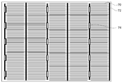
また、図2及び3に示すように、アルミニウム電極と櫛歯で対応するように、銀電極の幅方向の中心から中心までの距離が1000μmとなるように、公知の銀ペーストを印刷幅50μmで印刷し、100℃で10分乾燥させた(図1(h))。次に、ベルト炉にてピーク温度を900℃に設定して焼成した(図1(i))。この焼成により、アルミニウム電極(p+層を含む)が形成されるとともに、銀電極がn+層の表面に形成される。
また、図2及び3に示すように、アルミニウム電極と櫛歯で対応するように、銀電極の幅方向の中心から中心までの距離が1000μmとなるように、公知の銀ペーストを印刷幅50μmで印刷し、100℃で10分乾燥させた(図1(h))。次に、ベルト炉にてピーク温度を900℃に設定して焼成した(図1(i))。この焼成により、アルミニウム電極(p+層を含む)が形成されるとともに、銀電極がn+層の表面に形成される。
以上のようにして、バックコンタクト型太陽電池セルを得た。
実施例1は工程が簡素であるため、バックコンタクト型太陽電池セル製造に要した時間は260分間であった。
なお、参考までに、実施例1において、工程(A)及び工程(B)を実施しない態様との比較ではバックコンタクト型太陽電池セル製造に要した時間の差は30分間であった。製造コスト、リーク電流抑制効果の点では、リーク電流の抑制により開放電圧Voc特性が1.5%向上し、曲線因子特性が2.5%向上したことにより単位発電量当たりの製造コストの削減が認められた。
(比較例1)
従来技術と同様に、結晶シリコン基板の受光面表面をテクスチャエッチングすることにより凹凸形状を形成し、結晶シリコン基板の全面に接するようにシリコン酸化膜を形成し、更にシリコン薄膜層(アモルファスシリコン薄膜層)を形成し、併せて結晶シリコン基板の表面及び裏面にn+層とp+層を形成するためにイオン注入法により不純物注入を繰り返してバックコンタクト型太陽電池セルを得た。具体的な手順を以下に詳述する。
(比較例1)
従来技術と同様に、結晶シリコン基板の受光面表面をテクスチャエッチングすることにより凹凸形状を形成し、結晶シリコン基板の全面に接するようにシリコン酸化膜を形成し、更にシリコン薄膜層(アモルファスシリコン薄膜層)を形成し、併せて結晶シリコン基板の表面及び裏面にn+層とp+層を形成するためにイオン注入法により不純物注入を繰り返してバックコンタクト型太陽電池セルを得た。具体的な手順を以下に詳述する。
先ずp型の単結晶シリコンからなる結晶シリコン基板を準備した(基板:6inch、厚み200μm)。準備した結晶シリコン基板の切断面ダメージ層の除去する目的で結晶シリコン基板の表裏をフッ酸と硝酸の混合溶液等の溶液でウエットエッチングした。
続いて前記結晶シリコン基板を硝酸溶液に浸漬させることにより両面にシリコン酸化膜を形成した。
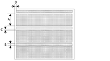
続いて、両面に200nmのシリコン薄膜層(アモルファスシリコン薄膜層)を形成した。裏面のシリコン薄膜層へレジストマスクを使用したイオン注入法により、図4に示すように、p型拡散層とn型拡散層を交互に帯状に形成されているパターンを形成した。具体的には、n型拡散領域の幅(A)は700μm、p型拡散領域の幅(B)は200μm、n型拡散領域とp型拡散領域のスペース(C)は50μm、基板端に最も近い拡散層端と基板端間(D)は1000μmとした。その後、加熱炉にて875℃でアニールすることによりp+層,n+層の活性化とアモルファスシリコン薄膜層を多結晶シリコン薄膜層へと変性させた。
続いてプラズマCVD法によって酸化ケイ素からなるパッシベーション膜を約30~50nm形成した後、更に表面にALD法により酸化アルミニウムからなるパッシベーション膜を10~30nm形成した後、反射防止膜としてプラズマCVD法によってシランガス及びアンモニアガスを用いて、窒化ケイ素膜を結晶シリコン基板裏面に形成した。
続いて電極を形成するため、結晶シリコン基板裏面にパターニングを施し、アルミニウム蒸着によりアルミニウム電極を形成した。
その後、アルミニウムとコンタクトをとれるように、Ni,Cu、Agメッキを行い、アニール処理を行った。また、形成した電極をレーザー照射装置によりp+層とコンタクトを取る電極と、n+層へコンタクトを取る電極へ分離した。
以上のようにして、バックコンタクト型太陽電池セルを得た。
工程が複雑であるため所要した時間は350分間であった。
10 結晶シリコン基板
20 酸化膜
30A シリコン薄膜層
30B シリコン薄膜層(活性化アニール後)
40 n+層
50 パッシベーション膜
60A アルミニウム電極を形成するためのアルミニウムペースト
60B アルミニウム電極
60C アルミニウム-シリコン合金層
60D BSF層
70A 銀電極を形成するための銀ペースト
70B 銀電極
70 アルミニウム電極
72 銀電極
74 アルミニウム接合用銀電極
A n型拡散領域の幅
B p型拡散領域の幅
C n型拡散領域とp型拡散領域とのスペース
D 基板端に最も近い拡散層端と基板端とのスペース
1000 イオン注入装置
1001、1002 真空槽
1003 絶縁部材
1004 ステージ
1005 ガス供給源
1010 プラズマ
1100 RF導入コイル
1101 永久磁石
1102 RF導入窓
1200、1201 電極
1300 直流電源
1301 交流電源
S1 基板
20 酸化膜
30A シリコン薄膜層
30B シリコン薄膜層(活性化アニール後)
40 n+層
50 パッシベーション膜
60A アルミニウム電極を形成するためのアルミニウムペースト
60B アルミニウム電極
60C アルミニウム-シリコン合金層
60D BSF層
70A 銀電極を形成するための銀ペースト
70B 銀電極
70 アルミニウム電極
72 銀電極
74 アルミニウム接合用銀電極
A n型拡散領域の幅
B p型拡散領域の幅
C n型拡散領域とp型拡散領域とのスペース
D 基板端に最も近い拡散層端と基板端とのスペース
1000 イオン注入装置
1001、1002 真空槽
1003 絶縁部材
1004 ステージ
1005 ガス供給源
1010 プラズマ
1100 RF導入コイル
1101 永久磁石
1102 RF導入窓
1200、1201 電極
1300 直流電源
1301 交流電源
S1 基板
Claims (5)
- バックコンタクト型太陽電池セルの製造方法であって、
結晶シリコン基板の裏面に酸化膜を形成する工程(A)、
前記酸化膜の露出面にシリコン薄膜層を形成する工程(B)、
前記シリコン薄膜層にメカニカルハードマスクを用いたイオン注入法及び活性化アニールによりn+層を部分的に形成する工程(C)、
前記工程(C)で得られた、前記酸化膜、前記シリコン薄膜層及び前記n+層を有する前記結晶シリコン基板の両面にパッシベーション膜を形成する工程(D)、及び
前記結晶シリコン基板の裏面側に形成された前記パッシベーション膜のうち前記n+層を被覆していない領域の一部を除去し、露出した前記シリコン薄膜層に1つ又は複数のアルミニウム電極を形成する工程(E)、
を順に有することを特徴とする、バックコンタクト型太陽電池セルの製造方法。 - 前記工程(D)の後に、前記結晶シリコン基板の裏面側に形成された前記パッシベーション膜のうち前記結晶シリコン基板を前記酸化膜及び前記n+層を介して被覆している領域の一部を除去し、露出した前記n+層に1つ又は複数の銀電極を形成する工程(E´)を有し、
前記工程(E)及び前記工程(E´)は順不同である、請求項1に記載の製造方法。 - 前記工程(E´)において、前記銀電極に代えて銅電極又はアルミニウム合金電極を形成する、請求項2に記載の製造方法。
- 前記アルミニウム電極は、アルミニウム粉末100質量部に対して有機ビヒクル2~20質量部及びガラスフリット0.15~15質量部を含有するアルミニウムペーストの塗膜を650~900℃で焼成することにより形成する、請求項1~3のいずれかに記載の製造方法。
- 前記結晶シリコン基板の裏面側において、前記アルミニウム電極と前記銀電極とが交互に配置されるように形成する、請求項2に記載の製造方法。
Priority Applications (2)
| Application Number | Priority Date | Filing Date | Title |
|---|---|---|---|
| US17/437,977 US20220173264A1 (en) | 2019-03-13 | 2020-03-13 | Method for producing back contact solar cell |
| CN202080020684.5A CN113785405B (zh) | 2019-03-13 | 2020-03-13 | 背接触型太阳能电池单元的制造方法 |
Applications Claiming Priority (2)
| Application Number | Priority Date | Filing Date | Title |
|---|---|---|---|
| JP2019045737A JP7264674B2 (ja) | 2019-03-13 | 2019-03-13 | バックコンタクト型太陽電池セルの製造方法 |
| JP2019-045737 | 2019-03-13 |
Publications (1)
| Publication Number | Publication Date |
|---|---|
| WO2020184706A1 true WO2020184706A1 (ja) | 2020-09-17 |
Family
ID=72426787
Family Applications (1)
| Application Number | Title | Priority Date | Filing Date |
|---|---|---|---|
| PCT/JP2020/011064 Ceased WO2020184706A1 (ja) | 2019-03-13 | 2020-03-13 | バックコンタクト型太陽電池セルの製造方法 |
Country Status (4)
| Country | Link |
|---|---|
| US (1) | US20220173264A1 (ja) |
| JP (1) | JP7264674B2 (ja) |
| CN (1) | CN113785405B (ja) |
| WO (1) | WO2020184706A1 (ja) |
Families Citing this family (3)
| Publication number | Priority date | Publication date | Assignee | Title |
|---|---|---|---|---|
| WO2021046258A1 (en) * | 2019-09-04 | 2021-03-11 | Unm Rainforest Innovations | Flexibility-assisted heat removal in thin crystalline silicon solar cells |
| CN112436024B (zh) * | 2020-11-20 | 2024-02-27 | 武汉新芯集成电路制造有限公司 | 背照式图像传感器及其制作方法 |
| CN115332366B (zh) * | 2022-07-21 | 2025-03-11 | 中国电子科技集团公司第四十八研究所 | 一种背钝化接触异质结太阳电池及其制备方法 |
Citations (6)
| Publication number | Priority date | Publication date | Assignee | Title |
|---|---|---|---|---|
| JP2013048146A (ja) * | 2011-08-29 | 2013-03-07 | Kyocera Corp | 太陽電池モジュール |
| KR20130090606A (ko) * | 2012-02-06 | 2013-08-14 | 엘지전자 주식회사 | 태양 전지의 제조 방법 |
| CN103943693A (zh) * | 2014-04-30 | 2014-07-23 | 山东力诺太阳能电力股份有限公司 | 一种p型硅衬底背面接触式太阳电池结构和制备方法 |
| JP2016506627A (ja) * | 2012-12-21 | 2016-03-03 | サンパワー コーポレイション | 太陽電池の拡散領域を形成する方法 |
| CN106299024A (zh) * | 2016-08-26 | 2017-01-04 | 泰州中来光电科技有限公司 | 一种背接触太阳能电池的制备方法及其电池和组件、系统 |
| CN106374009A (zh) * | 2016-09-20 | 2017-02-01 | 泰州中来光电科技有限公司 | 一种钝化接触的ibc电池及其制备方法和组件、系统 |
Family Cites Families (11)
| Publication number | Priority date | Publication date | Assignee | Title |
|---|---|---|---|---|
| DE602006021767D1 (de) * | 2005-10-20 | 2011-06-16 | Toyo Aluminium Kk | Pastenzusammensetzung und solarbatterieelement damit |
| US8492253B2 (en) * | 2010-12-02 | 2013-07-23 | Sunpower Corporation | Method of forming contacts for a back-contact solar cell |
| JP2014154656A (ja) * | 2013-02-07 | 2014-08-25 | Dainippon Screen Mfg Co Ltd | 結晶シリコン型太陽電池、およびその製造方法 |
| CN103811591B (zh) * | 2014-02-27 | 2016-10-05 | 友达光电股份有限公司 | 背接触式太阳能电池的制作方法 |
| WO2016125803A1 (ja) * | 2015-02-02 | 2016-08-11 | 京セラ株式会社 | 太陽電池素子およびその製造方法 |
| EP3184670B1 (en) * | 2015-12-23 | 2019-04-17 | Repsol, S.A. | Substrate-electrode (se) interface illuminated photoelectrodes and photoelectrochemical cells |
| JP6688244B2 (ja) * | 2017-03-01 | 2020-04-28 | 信越化学工業株式会社 | 高効率太陽電池の製造方法及び太陽電池セルの製造システム |
| DE102017108077A1 (de) * | 2017-04-13 | 2018-10-18 | Hanwha Q Cells Gmbh | Solarzellen-Herstellungsverfahren |
| KR20180127597A (ko) * | 2017-05-19 | 2018-11-29 | 오씨아이 주식회사 | 후면접합 실리콘 태양전지 및 이를 제조하는 방법 |
| US11145774B2 (en) * | 2018-05-30 | 2021-10-12 | Solar Inventions Llc | Configurable solar cells |
| CN108666376B (zh) * | 2018-07-11 | 2023-08-08 | 泰州隆基乐叶光伏科技有限公司 | 一种p型背接触太阳电池及其制备方法 |
-
2019
- 2019-03-13 JP JP2019045737A patent/JP7264674B2/ja active Active
-
2020
- 2020-03-13 WO PCT/JP2020/011064 patent/WO2020184706A1/ja not_active Ceased
- 2020-03-13 CN CN202080020684.5A patent/CN113785405B/zh active Active
- 2020-03-13 US US17/437,977 patent/US20220173264A1/en active Pending
Patent Citations (6)
| Publication number | Priority date | Publication date | Assignee | Title |
|---|---|---|---|---|
| JP2013048146A (ja) * | 2011-08-29 | 2013-03-07 | Kyocera Corp | 太陽電池モジュール |
| KR20130090606A (ko) * | 2012-02-06 | 2013-08-14 | 엘지전자 주식회사 | 태양 전지의 제조 방법 |
| JP2016506627A (ja) * | 2012-12-21 | 2016-03-03 | サンパワー コーポレイション | 太陽電池の拡散領域を形成する方法 |
| CN103943693A (zh) * | 2014-04-30 | 2014-07-23 | 山东力诺太阳能电力股份有限公司 | 一种p型硅衬底背面接触式太阳电池结构和制备方法 |
| CN106299024A (zh) * | 2016-08-26 | 2017-01-04 | 泰州中来光电科技有限公司 | 一种背接触太阳能电池的制备方法及其电池和组件、系统 |
| CN106374009A (zh) * | 2016-09-20 | 2017-02-01 | 泰州中来光电科技有限公司 | 一种钝化接触的ibc电池及其制备方法和组件、系统 |
Also Published As
| Publication number | Publication date |
|---|---|
| CN113785405B (zh) | 2025-10-17 |
| JP2020150111A (ja) | 2020-09-17 |
| US20220173264A1 (en) | 2022-06-02 |
| JP7264674B2 (ja) | 2023-04-25 |
| CN113785405A (zh) | 2021-12-10 |
Similar Documents
| Publication | Publication Date | Title |
|---|---|---|
| US8168462B2 (en) | Passivation process for solar cell fabrication | |
| CN101414648B (zh) | 结晶硅太阳能电池的快速氢钝化的方法 | |
| EP3151286B1 (en) | Solar cell element, method for manufacturing same and solar cell module | |
| US10840395B2 (en) | Deposition approaches for emitter layers of solar cells | |
| US20100024872A1 (en) | Semiconductor layer manufacturing method, semiconductor layer manufacturing apparatus, and semiconductor device manufactured using such method and apparatus | |
| CN112864275B (zh) | Ibc电池的制备方法、ibc电池和太阳能电池组件 | |
| US20140261666A1 (en) | Methods of manufacturing a low cost solar cell device | |
| CN113785405B (zh) | 背接触型太阳能电池单元的制造方法 | |
| CN117276359A (zh) | 一种隧穿氧化多层结构及其制备方法与应用 | |
| JP2019110185A (ja) | 太陽電池の製造方法 | |
| WO2012169319A1 (ja) | 太陽電池の製造方法 | |
| CN117766623A (zh) | 一种太阳电池的制备方法、太阳电池及光伏组件 | |
| TWI463687B (zh) | A film forming method of a passivation film, and a method for manufacturing a solar cell element | |
| US20230076597A1 (en) | Passivated contact solar cell and fabrication method for back passivation assembly thereof | |
| WO2013008482A1 (ja) | 太陽電池およびその製造方法 | |
| JP7264673B2 (ja) | バックコンタクト型太陽電池セルの製造方法 | |
| JP2014075418A (ja) | 太陽電池用シリコン基板及びその製造方法、並びに太陽電池 | |
| JP2004281569A (ja) | 太陽電池素子の製造方法 | |
| JP2003101048A (ja) | 光起電力装置の製造方法 | |
| CN110809827A (zh) | 光电转换装置的制造方法 | |
| CN112635619A (zh) | 晶硅太阳能电池多层膜的等离子体处理方法及太阳能电池 | |
| KR20090132541A (ko) | 기판형 태양전지의 제조방법 | |
| JP5933198B2 (ja) | 結晶太陽電池の製造方法 | |
| JP2006344883A (ja) | 太陽電池の製造方法 | |
| JP2020170830A (ja) | TOPCon−BC構造の結晶系太陽電池の製造方法、及びTOPCon−BC構造の結晶系太陽電池 |
Legal Events
| Date | Code | Title | Description |
|---|---|---|---|
| 121 | Ep: the epo has been informed by wipo that ep was designated in this application |
Ref document number: 20769647 Country of ref document: EP Kind code of ref document: A1 |
|
| NENP | Non-entry into the national phase |
Ref country code: DE |
|
| 122 | Ep: pct application non-entry in european phase |
Ref document number: 20769647 Country of ref document: EP Kind code of ref document: A1 |
|
| WWG | Wipo information: grant in national office |
Ref document number: 202080020684.5 Country of ref document: CN |