WO2020184510A1 - 接合基板及び接合基板の製造方法 - Google Patents
接合基板及び接合基板の製造方法 Download PDFInfo
- Publication number
- WO2020184510A1 WO2020184510A1 PCT/JP2020/009983 JP2020009983W WO2020184510A1 WO 2020184510 A1 WO2020184510 A1 WO 2020184510A1 JP 2020009983 W JP2020009983 W JP 2020009983W WO 2020184510 A1 WO2020184510 A1 WO 2020184510A1
- Authority
- WO
- WIPO (PCT)
- Prior art keywords
- copper plate
- silicon nitride
- substrate
- nitride ceramic
- ceramic substrate
- Prior art date
- Legal status (The legal status is an assumption and is not a legal conclusion. Google has not performed a legal analysis and makes no representation as to the accuracy of the status listed.)
- Ceased
Links
Images



Classifications
-
- H—ELECTRICITY
- H05—ELECTRIC TECHNIQUES NOT OTHERWISE PROVIDED FOR
- H05K—PRINTED CIRCUITS; CASINGS OR CONSTRUCTIONAL DETAILS OF ELECTRIC APPARATUS; MANUFACTURE OF ASSEMBLAGES OF ELECTRICAL COMPONENTS
- H05K1/00—Printed circuits
- H05K1/02—Details
- H05K1/03—Use of materials for the substrate
-
- H—ELECTRICITY
- H05—ELECTRIC TECHNIQUES NOT OTHERWISE PROVIDED FOR
- H05K—PRINTED CIRCUITS; CASINGS OR CONSTRUCTIONAL DETAILS OF ELECTRIC APPARATUS; MANUFACTURE OF ASSEMBLAGES OF ELECTRICAL COMPONENTS
- H05K3/00—Apparatus or processes for manufacturing printed circuits
- H05K3/38—Improvement of the adhesion between the insulating substrate and the metal
-
- H—ELECTRICITY
- H10—SEMICONDUCTOR DEVICES; ELECTRIC SOLID-STATE DEVICES NOT OTHERWISE PROVIDED FOR
- H10W—GENERIC PACKAGES, INTERCONNECTIONS, CONNECTORS OR OTHER CONSTRUCTIONAL DETAILS OF DEVICES COVERED BY CLASS H10
- H10W70/00—Package substrates; Interposers; Redistribution layers [RDL]
- H10W70/60—Insulating or insulated package substrates; Interposers; Redistribution layers
- H10W70/67—Insulating or insulated package substrates; Interposers; Redistribution layers characterised by their insulating layers or insulating parts
- H10W70/68—Shapes or dispositions thereof
Definitions
- the present invention relates to a bonded substrate and a method for manufacturing the bonded substrate.
- Silicon nitride ceramics have high thermal conductivity and high insulation. Therefore, a bonded substrate in which a copper plate is bonded to a silicon nitride ceramic substrate via a bonding layer is suitably used as an insulating heat-dissipating substrate on which a power semiconductor element is mounted.
- the bonded substrate is produced by producing an intermediate product in which the brazing material layer is between the copper plate and the silicon nitride ceramic substrate, and the produced intermediate product is heat-treated to change the brazing material layer into a bonded layer, and the copper plate And manufactured by patterning the bonding layer.
- the copper circuit board is joined to at least one surface of the ceramic substrate formed of silicon nitride via a brazing material layer (paragraphs 0013 and 0020). ..
- the ceramic circuit board includes a brazing material layer interposed between the copper circuit board and the ceramics circuit board, and a brazing material protruding portion protruding outward from the side surface of the copper circuit board (paragraph 0013).
- the brazing filler metal layer is formed from a brazing filler metal containing Ag, Cu and Ti (paragraph 0013).
- the present invention has been made in consideration of this problem.
- the problem to be solved by the present invention is to suppress the movement of silver from the protruding portion due to the ion migration phenomenon while suppressing the defect of the bonded substrate due to the concentration of stress on the end portion of the copper plate, and to suppress the movement of silver from the protruding portion. It is to suppress the defect of the bonded substrate due to the movement of silver.
- the present invention is directed to a bonded substrate.
- the bonding substrate includes a silicon nitride ceramic substrate, a copper plate, and a bonding layer.
- a copper plate is bonded to a silicon nitride ceramic substrate.
- the copper plate and the bonding layer are arranged on the silicon nitride ceramic substrate.
- the bonding layer includes an inter-plate portion between the silicon nitride ceramic substrate and the copper plate, and a protruding portion protruding from between the silicon nitride ceramic substrate and the copper plate.
- the protruding part does not contain silver.
- the present invention is also directed to a method for manufacturing a bonded substrate.
- a brazing material layer is formed on the silicon nitride ceramic substrate.
- the brazing filler metal layer comprises a metal powder containing silver and an active metal brazing filler metal containing at least one hydrogenated metal powder selected from the group consisting of titanium hydride powder and zirconium hydride powder.
- the intermediate product is formed by a hot press.
- the silver contained in the metal powder diffuses into the copper plate.
- the brazing material layer changes to a bonding layer for bonding the copper plate to the silicon nitride ceramic substrate.
- the patterned bonding layer includes an inter-plate portion between the silicon nitride ceramic substrate and the patterned copper plate, and a protruding portion protruding from between the silicon nitride ceramic substrate and the patterned copper plate.
- the concentration of stress on the end portion of the copper plate is relaxed by the protruding portion. As a result, it is possible to suppress defects in the bonded substrate due to stress concentration on the ends of the copper plate.
- the protruding portion does not contain silver. Therefore, it is possible to suppress the movement of silver from the protruding portion due to the ion migration phenomenon. As a result, it is possible to suppress defects in the bonded substrate due to the movement of silver from the protruding portion.
- FIG. 5 is an enlarged cross-sectional view schematically showing a part of the bonded substrate of the first embodiment. It is a flowchart which shows the manufacturing flow of the bonded substrate of 1st Embodiment. It is sectional drawing which shows typically the intermediate product obtained in the process of manufacturing the bonded substrate of 1st Embodiment. It is sectional drawing which shows typically the intermediate product obtained in the process of manufacturing the bonded substrate of 1st Embodiment. It is sectional drawing which shows typically the intermediate product obtained in the process of manufacturing the bonded substrate of 1st Embodiment. It is sectional drawing which shows typically the intermediate product obtained in the process of manufacturing the bonded substrate of 1st Embodiment.
- FIG. 1 It is a flowchart which shows the flow of the patterning of the copper plate and the bonding layer in the manufacturing of the bonding substrate of 1st Embodiment. It is sectional drawing which shows typically the intermediate product obtained in the process of patterning of a copper plate and a bonding layer in the manufacturing of the bonding substrate of 1st Embodiment. It is sectional drawing which shows typically the intermediate product obtained in the process of patterning of a copper plate and a bonding layer in the manufacturing of the bonding substrate of 1st Embodiment. It is sectional drawing which shows typically the bonding substrate compared with the bonding substrate of Embodiment 1. FIG.
- FIG. 1 is a cross-sectional view schematically showing the bonded substrate of the first embodiment.
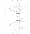
- FIG. 2 is an enlarged cross-sectional view schematically showing a part of the bonded substrate of the first embodiment.
- FIG. 2 is an enlarged view of a part A of FIG.
- the bonding substrate 100 of the first embodiment includes a silicon nitride ceramic substrate 110, a copper plate 111, a bonding layer 112, a copper plate 113, and a bonding layer 114.
- the bonded substrate 100 may include elements other than these elements.
- One of the set of the copper plate 111 and the bonding layer 112 and the set of the copper plate 113 and the bonding layer 114 may be omitted.
- the copper plates 111 and 113 are bonded to the silicon nitride ceramic substrate 110 via the bonding layers 112 and 114, respectively.
- the copper plates 111 and 113 are brazed to the main surfaces 1101 and 1102 of the silicon nitride ceramic substrate 110 by the active metal brazing method by the bonding layers 112 and 114, respectively.
- the bonded substrate 100 may be used in any way, and is used, for example, as an insulated heat-dissipating substrate on which a power semiconductor element is mounted.
- the copper plate 111 and the bonding layer 112 are arranged on the main surface 1101 of the silicon nitride ceramic substrate 110 as shown in FIGS. 1 and 2.
- the copper plate 113 and the bonding layer 114 are arranged on the main surface 1102 of the silicon nitride ceramic substrate 110 as shown in FIG.
- the bonding layers 112 and 114 join the copper plates 111 and 113 to the main surfaces 1101 and 1102 of the silicon nitride ceramic substrate 110, respectively.
- the joint layer 112 includes an inter-plate portion 120 and a protruding portion 121.
- the inter-plate portion 120 is located between the silicon nitride ceramic substrate 110 and the copper plate 111.
- the protruding portion 121 protrudes from between the silicon nitride ceramic substrate 110 and the copper plate 111.
- the bonding layer 114 includes an inter-plate portion 122 and a protruding portion 123.
- the inter-plate portion 122 is located between the silicon nitride ceramic substrate 110 and the copper plate 113.
- the protruding portion 123 protrudes from between the silicon nitride ceramic substrate 110 and the copper plate 113.
- the concentration of stress on the ends of the copper plates 111 and 113 is relaxed by the protruding portions 121 and 123, respectively. As a result, it is possible to suppress defects in the bonded substrate 100 due to stress concentration on the ends of the copper plates 111 and 113.
- the bonding layers 112 and 114 preferably have a thickness of 0.1 ⁇ m or more and 3 ⁇ m or less. Since the bonding layers 112 and 114 have such a small thickness, the concentration of stress on the ends of the copper plates 111 and 113 is effectively alleviated by the protruding portions 121 and 123, respectively.
- the bonding layers 112 and 114 shown in FIGS. 1 and 2 are formed by at least one element selected from the group consisting of titanium (Ti) and zirconium (Zr) and nitrogen ( Contains compounds with at least one element selected from the group consisting of N) and silicon (Si), but does not contain silver (Ag). Therefore, the protruding portions 121 and 123 also contain a compound of at least one element selected from the group consisting of titanium and zirconium and at least one element selected from the group consisting of nitrogen and silicon, but contain silver. Not included. Therefore, it is possible to suppress the movement of silver from the protruding portions 121 and 123 due to the ion migration phenomenon.
- the bonding layers 112 and 114 consist only of a compound of at least one element preferably selected from the group consisting of titanium and zirconium and at least one element selected from the group consisting of nitrogen and silicon.
- the protruding portions 121 and 123 are also preferably composed of only a compound of at least one element selected from the group consisting of titanium and zirconium and at least one element selected from the group consisting of nitrogen and silicon. Further, the bonding layers 112 and 114 do not contain elements such as tin (Sn) and phosphorus (P) that promote the above-mentioned ion migration phenomenon.
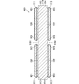
- FIG. 10 is a cross-sectional view schematically showing a bonded substrate to be compared with the bonded substrate of the first embodiment.
- the bonded substrate 900 shown in FIG. 10 does not include protruding portions 121 and 123. Due to this, the bonded substrate 900 has a gap 921 formed between the silicon nitride ceramic substrate 110 and the copper plate 111, and a gap 923 formed between the silicon nitride ceramic substrate 110 and the copper plate 113. Have.
- Providing the protruding portion 121 prevents the formation of the void 921. Further, providing the protruding portion 123 prevents the formation of the void 923.
- the protruding portion 121 prevents the formation of the void 921.
- the protruding portion 123 prevents the formation of the void 923.
- the composite when the composite is molded with a resin, it is possible to prevent the formation of voids 921 and 923 in which the resin does not easily penetrate, and voids causing insulation failure are caused by the voids 921 and 923. Can be prevented from remaining.
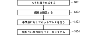
- FIG. 3 is a flowchart showing a flow of manufacturing a bonded substrate according to the first embodiment.
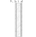
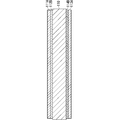
- 4, 5 and 6 are cross-sectional views schematically illustrating an intermediate product obtained in the process of manufacturing the bonded substrate of the first embodiment.
- steps S101 to S104 shown in FIG. 3 are sequentially executed.
- step S101 as shown in FIG. 4, brazing material layers 132 and 134 are formed on the main surfaces 1101 and 1102 of the silicon nitride ceramic substrate 110, respectively.
- the formation of the brazing material layer 132 is omitted.
- the formation of the brazing material layer 134 is omitted.
- a paste containing an active metal brazing filler metal and a solvent is prepared.
- the paste may further contain binders, dispersants, defoamers and the like.
- the prepared paste is screen-printed on the main surfaces 1101 and 1102 of the silicon nitride ceramic substrate 110, and the first and second screen-printed films are formed on the main surfaces 1101 and 1102 of the silicon nitride ceramic substrate 110, respectively. Will be done.
- the solvent contained in the formed first and second screen printing films is volatilized. As a result, the first and second screen printing films are changed to the brazing filler metal layers 132 and 134, respectively.
- the brazing filler metal layers 132 and 134 include an active metal brazing filler metal.
- the brazing filler metal layers 132 and 134 may be formed by a method different from this method.
- the active metal brazing material is selected from the group consisting of metal powders containing silver (Ag), copper (Cu) and indium (In), and titanium hydride (TiH 2 ) powder and zirconium hydride (ZrH 2 ) powder. Contains at least one metal hydride powder.
- the composition of the active metal brazing material may be changed. For example, both or one of copper and indium may not be contained in the metal powder, and metal elements other than copper and indium may be contained in the metal powder.
- the active metal brazing material preferably contains 40% by weight or more and 80% by weight or less of silver. Since the active metal brazing material contains only a small amount of silver in this way, it becomes easy to diffuse silver to the copper plates 111A and 113A and eliminate silver from the bonding layers 112B and 114B in the step S103 described below.
- the active metal brazing material preferably consists of a powder having an average particle size of 0.1 ⁇ m or more and 10 ⁇ m or less.
- the average particle size can be obtained by measuring the particle size distribution with a commercially available laser diffraction type particle size distribution measuring device and calculating D50 from the measured particle size distribution. Since the active metal brazing material is composed of a powder having such a small average particle size, the brazing material layers 132 and 134 can be thinned.
- the brazing filler metal layers 132 and 134 preferably have a thickness of 0.1 ⁇ m or more and 5 ⁇ m or less. Since the brazing filler metal layers 132 and 134 have such a small thickness, the amount of silver contained in the brazing filler metal layers 132 and 134 is reduced, and silver is diffused and joined to the copper plates 111A and 113A in the step S103 described below. It facilitates the elimination of silver from layers 112B and 114B.
- step S102 as shown in FIG. 5, copper plates 111A and 113A are arranged on the brazing material layers 132 and 134 formed, respectively.
- an intermediate product 100A including the silicon nitride ceramic substrate 110, the copper plate 111A, the brazing material layer 132, the copper plate 113A, and the brazing material layer 134 can be obtained.
- the arrangement of the copper plate 111A is omitted.
- the arrangement of the copper plate 113A is omitted.
- step S103 hot pressing is performed on the obtained intermediate product 100A.
- the brazing filler metal layers 132 and 134 are changed to the bonding layers 112B and 114B, respectively, as shown in FIG.
- the bonding layers 112B and 114B bond the copper plates 111A and 113A to the silicon nitride ceramic substrate 110, respectively.
- the brazing layers 132 and 134 change to the bonding layers 112B and 114B, respectively, the silver and indium contained in the brazing layers 132 and 134 diffuse into the copper plates 111A and 113A, respectively, and the silver and indium from the bonding layers 112B and 114B. Indium disappears.
- the bonding layers 112B and 114B contain a compound of at least one element selected from the group consisting of titanium and zirconium and at least one element selected from the group consisting of nitrogen and silicon, but contain silver. Not included. At least one element selected from the group consisting of nitrogen and silicon is supplied from the silicon nitride ceramic substrate 110.
- the intermediate product 100A is pressurized in the thickness direction of the silicon nitride ceramic substrate 110 according to the surface pressure profile such that the maximum surface pressure is 5 MPa or more and 25 MPa or less in vacuum or an inert gas. , It is heated according to a temperature profile such that the maximum temperature is 800 ° C. or higher and 900 ° C. or lower.
- the brazing filler metal layers 132 and 134 are thin, such as when the brazing filler metal layers 132 and 134 have a thickness of 0.1 ⁇ m or more and 5 ⁇ m or less, the copper plates 111A and 113A are made of silicon nitride without forming voids.
- the brazing filler metal layers 132 and 134 can be thinned without forming voids, the amount of silver contained in the brazing filler metal layers 132 and 134 can be reduced, and silver is diffused to the copper plates 111A and 113A to form a bonding layer. It becomes easy to eliminate silver from 112B and 114B. Further, the shape of the particles constituting the active metal brazing material is changed to a layered shape, and silver or the like is diffused into the copper plates 111A and 113A, so that the bonding layers 112B and 114B are substantially 0.1 ⁇ m or more and 3 ⁇ m or less. Will have the thickness of.
- step S104 the copper plate 111A, the bonding layer 112B, the copper plate 113A, and the bonding layer 114B are patterned.
- the copper plates 111A and 113A are changed to the patterned copper plates 111 and 113 shown in FIG. 1, respectively.
- the bonding layers 112B and 114B are changed to the patterned bonding layers 112 and 114 shown in FIG. 1, respectively.
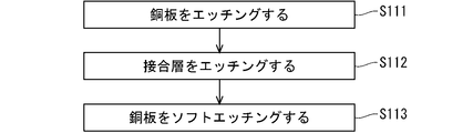
- FIG. 7 is a flowchart showing the flow of patterning of the copper plate and the bonding layer in the production of the bonding substrate of the first embodiment.
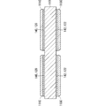
- 8 and 9 are cross-sectional views schematically illustrating an intermediate product obtained in the process of patterning a copper plate and a bonding layer in the production of the bonding substrate of the first embodiment.
- the steps S111 to S113 shown in FIG. 7 are sequentially executed.
- step S111 the copper plates 111A and 113A are etched. As a result, a part of the copper plates 111A and 113A is removed, and as shown in FIG. 8, the copper plates 111A and 113A are changed to the etched copper plates 111C and 113C, respectively. Further, in the bonding layer 112B, a first portion 140 between the silicon nitride ceramic substrate 110 and the etched copper plate 111C and a second portion not between the silicon nitride ceramic substrate 110 and the etched copper plate 111C are formed. 141 is formed.
- a first portion 142 between the silicon nitride ceramics substrate 110 and the etched copper plate 113C and a second portion not between the silicon nitride ceramics substrate 110 and the etched copper plate 113C are formed.
- An etching solution such as an iron chloride aqueous solution system or a copper chloride aqueous solution system can be used for etching the copper plates 111A and 113A.
- step S112 as shown in FIG. 9, the formed second portions 141 and 143 are etched. As a result, the second portions 141 and 143 are removed, leaving the first portions 140 and 142. The remaining first portions 140 and 142 become the bonding layers 120 and 122, respectively.
- An etching solution such as an aqueous ammonium fluoride solution can be used for etching the second portions 141 and 143.
- both ends of the first portions 140 and 142 may be removed by etching.
- step S113 the etched copper plates 111C and 113C are soft-etched. As a result, the vicinity of the end portions of the etched copper plates 111C and 113C is removed. Further, the etched copper plates 111C and 113C are changed to the patterned copper plates 111 and 113 shown in FIG. 1, respectively. Further, the etched joint layers 140 and 142 are formed with the inter-plate portions 120 and 122 shown in FIG. 1, respectively, and the protruding portions 121 and 123 shown in FIG. 1, respectively.
- an etching solution such as an iron chloride aqueous solution system or a copper chloride aqueous solution system can be used. In step S113, even when both ends of the first portions 140 and 142 are removed by etching in step S112, the protruding portions 121 and 123 can be reliably formed.
Landscapes
- Engineering & Computer Science (AREA)
- Microelectronics & Electronic Packaging (AREA)
- Manufacturing & Machinery (AREA)
- Manufacturing Of Printed Wiring (AREA)
- Ceramic Products (AREA)
Abstract
銅板の端部への応力の集中に起因する接合基板の不良を抑制しながら、イオンマイグレーション現象によりはみ出し部から銀が移動することを抑制し、はみ出し部からの銀の移動に起因する接合基板の不良を抑制する。接合基板は、窒化ケイ素セラミックス基板、銅板及び接合層を備える。接合層は、銅板を窒化ケイ素セラミックス基板に接合する。銅板及び接合層は、窒化ケイ素セラミックス基板上に配置される。接合層は、窒化ケイ素セラミックス基板と銅板との間にある板間部、及び窒化ケイ素セラミックス基板と銅板との間からはみ出すはみ出し部を備える。はみ出し部は、銀を含まない。
Description
本発明は、接合基板及び接合基板の製造方法に関する。
窒化ケイ素セラミックスは、高い熱伝導性及び高い絶縁性を有する。このため、銅板が接合層を介して窒化ケイ素セラミックス基板に接合された接合基板は、パワー半導体素子が実装される絶縁放熱基板として好適に用いられる。
当該接合基板は、多くの場合は、ろう材層が銅板と窒化ケイ素セラミックス基板との間にある中間品を作製し、作製した中間品を熱処理してろう材層を接合層に変化させ、銅板及び接合層をパターニングすることにより製造される。
銅板の端部への応力の集中に起因する接合基板の不良を抑制するために、接合層に、窒化ケイ素セラミックス基板と銅板との間からはみ出すはみ出し部を形成することが提案されている。
例えば、特許文献1に記載されたセラミックス回路基板においては、銅回路板が、ろう材層を介して、窒化珪素から形成されたセラミックス基板の少なくとも一方の面に接合される(段落0013及び0020)。セラミックス回路基板は、銅回路板とセラミックス基板との間に介在されたろう材層、及び銅回路板の側面から外側にはみ出したろう材はみ出し部を備える(段落0013)。ろう材層は、Ag、Cu及びTiを含むろう材から形成される(段落0013)。
特許文献1に記載されたセラミックス回路基板に代表される従来の技術においては、イオンマイグレーション現象により窒化ケイ素セラミックス基板と銅板との間からはみ出すはみ出し部から銀が移動し、はみ出し部からの銀の移動に起因する接合基板の不良が発生する場合がある。例えば、85℃85%RHの環境下で数kV/mmの直流電界又は交流電界が印加された場合に、はみ出し部からの銀の移動に起因する接合基板の不良が発生する場合がある。
本発明は、この問題を考慮してなされた。本発明が解決しようとする課題は、銅板の端部への応力の集中に起因する接合基板の不良を抑制しながら、イオンマイグレーション現象によりはみ出し部から銀が移動することを抑制し、はみ出し部からの銀の移動に起因する接合基板の不良を抑制することである。
本発明は、接合基板に向けられる。
接合基板は、窒化ケイ素セラミックス基板、銅板及び接合層を備える。接合層は、銅板を窒化ケイ素セラミックス基板に接合する。
銅板及び接合層は、窒化ケイ素セラミックス基板上に配置される。接合層は、窒化ケイ素セラミックス基板と銅板との間にある板間部、及び窒化ケイ素セラミックス基板と銅板との間からはみ出すはみ出し部を備える。
はみ出し部は、銀を含まない。
本発明は、接合基板の製造方法にも向けられる。
接合基板の製造方法においては、窒化ケイ素セラミックス基板上に、ろう材層が形成される。ろう材層は、銀を含む金属粉末、並びに水素化チタン粉末及び水素化ジルコニウム粉末からなる群より選択される少なくとも1種の水素化金属粉末を含む活性金属ろう材を含む。
続いて、ろう材層上に銅板が配置される。これにより、窒化ケイ素セラミックス基板、銅板及びろう材層を備える中間品が得られる。
続いて、中間品に対してホットプレスが行われる。これにより、金属粉末に含まれる銀が、銅板に拡散する。また、ろう材層が、銅板を窒化ケイ素セラミックス基板に接合する接合層に変化する。
続いて、銅板及び接合層がパターニングされる。これにより、銅板が、パターニングされた銅板に変化する。また、接合層が、パターニングされた接合層に変化する。パターニングされた接合層は、窒化ケイ素セラミックス基板とパターニングされた銅板との間にある板間部、及び窒化ケイ素セラミックス基板とパターニングされた銅板との間からはみ出すはみ出し部を備える。
本発明によれば、銅板の端部への応力の集中がはみ出し部により緩和される。これにより、銅板の端部への応力の集中に起因する接合基板の不良を抑制することができる。
また、本発明によれば、はみ出し部が、銀を含まない。このため、イオンマイグレーション現象によりはみ出し部から銀が移動することを抑制することができる。これにより、はみ出し部からの銀の移動に起因する接合基板の不良を抑制することができる。
この発明の目的、特徴、局面及び利点は、以下の詳細な説明と添付図面とによって、より明白となる。
1 接合基板
図1は、第1実施形態の接合基板を模式的に図示する断面図である。図2は、第1実施形態の接合基板の一部を模式的に図示する拡大断面図である。図2は、図1の一部Aを拡大して図示する。
図1は、第1実施形態の接合基板を模式的に図示する断面図である。図2は、第1実施形態の接合基板の一部を模式的に図示する拡大断面図である。図2は、図1の一部Aを拡大して図示する。
第1実施形態の接合基板100は、図1及び図2に図示されるように、窒化ケイ素セラミックス基板110、銅板111、接合層112、銅板113及び接合層114を備える。接合基板100がこれらの要素以外の要素を備えてもよい。銅板111及び接合層112の組、並びに銅板113及び接合層114の組の片方の組が省略されてもよい。
銅板111及び113は、それぞれ接合層112及び114を介して窒化ケイ素セラミックス基板110に接合されている。銅板111及び113は、それぞれ接合層112及び114により窒化ケイ素セラミックス基板110の主面1101及び1102に活性金属ろう付け法によりろう付けされている。
接合基板100は、どのように用いられてもよいが、例えばパワー半導体素子が実装される絶縁放熱基板として用いられる。
2 銅板の端部への応力の集中の緩和
銅板111及び接合層112は、図1及び図2に図示されるように、窒化ケイ素セラミックス基板110の主面1101上に配置される。銅板113及び接合層114は、図1に図示されるように、窒化ケイ素セラミックス基板110の主面1102上に配置される。
銅板111及び接合層112は、図1及び図2に図示されるように、窒化ケイ素セラミックス基板110の主面1101上に配置される。銅板113及び接合層114は、図1に図示されるように、窒化ケイ素セラミックス基板110の主面1102上に配置される。
接合層112及び114は、それぞれ銅板111及び113を窒化ケイ素セラミックス基板110の主面1101及び1102に接合する。
接合層112は、板間部120及びはみ出し部121を備える。板間部120は、窒化ケイ素セラミックス基板110と銅板111との間にある。はみ出し部121は、窒化ケイ素セラミックス基板110と銅板111との間からはみ出す。接合層114は、板間部122及びはみ出し部123を備える。板間部122は、窒化ケイ素セラミックス基板110と銅板113との間にある。はみ出し部123は、窒化ケイ素セラミックス基板110と銅板113との間からはみ出す。接合基板100においては、銅板111及び113の端部への応力の集中が、それぞれはみ出し部121及び123により緩和される。これにより、銅板111及び113の端部への応力の集中に起因する接合基板100の不良を抑制することができる。
接合層112及び114は、望ましくは0.1μm以上3μm以下の厚さを有する。接合層112及び114がこのようにわずかな厚さしか有しないことにより、銅板111及び113の端部への応力の集中がそれぞれはみ出し部121及び123により効果的に緩和される。
3 はみ出し部からの銀の移動の抑制
図1及び図2に図示される接合層112及び114は、チタン(Ti)及びジルコニウム(Zr)からなる群より選択される少なくとも1種の元素と窒素(N)及びケイ素(Si)からなる群より選択される少なくとも1種の元素との化合物を含むが、銀(Ag)を含まない。このため、はみ出し部121及び123も、チタン及びジルコニウムからなる群より選択される少なくとも1種の元素と窒素及びケイ素からなる群より選択される少なくとも1種の元素との化合物を含むが、銀を含まない。このため、イオンマイグレーション現象によりはみ出し部121及び123から銀が移動することを抑制することができる。これにより、はみ出し部121及び123からの銀の移動に起因する接合基板100の不良を抑制することができる。ここでいうはみ出し部121及び123が銀を含まないことは、はみ出し部121及び123がイオンマイグレーション現象を発生させる濃度を有する銀を含まないことを意味し、痕跡量の銀を含むことを除外しない。接合層112及び114は、望ましくはチタン及びジルコニウムからなる群より選択される少なくとも1種の元素と窒素及びケイ素からなる群より選択される少なくとも1種の元素との化合物のみからなる。このため、はみ出し部121及び123も、望ましくはチタン及びジルコニウムからなる群より選択される少なくとも1種の元素と窒素及びケイ素からなる群より選択される少なくとも1種の元素との化合物のみからなる。また、接合層112及び114は、スズ(Sn)、リン(P)等の上述したイオンマイグレーション現象を促進する元素を含まない。
図1及び図2に図示される接合層112及び114は、チタン(Ti)及びジルコニウム(Zr)からなる群より選択される少なくとも1種の元素と窒素(N)及びケイ素(Si)からなる群より選択される少なくとも1種の元素との化合物を含むが、銀(Ag)を含まない。このため、はみ出し部121及び123も、チタン及びジルコニウムからなる群より選択される少なくとも1種の元素と窒素及びケイ素からなる群より選択される少なくとも1種の元素との化合物を含むが、銀を含まない。このため、イオンマイグレーション現象によりはみ出し部121及び123から銀が移動することを抑制することができる。これにより、はみ出し部121及び123からの銀の移動に起因する接合基板100の不良を抑制することができる。ここでいうはみ出し部121及び123が銀を含まないことは、はみ出し部121及び123がイオンマイグレーション現象を発生させる濃度を有する銀を含まないことを意味し、痕跡量の銀を含むことを除外しない。接合層112及び114は、望ましくはチタン及びジルコニウムからなる群より選択される少なくとも1種の元素と窒素及びケイ素からなる群より選択される少なくとも1種の元素との化合物のみからなる。このため、はみ出し部121及び123も、望ましくはチタン及びジルコニウムからなる群より選択される少なくとも1種の元素と窒素及びケイ素からなる群より選択される少なくとも1種の元素との化合物のみからなる。また、接合層112及び114は、スズ(Sn)、リン(P)等の上述したイオンマイグレーション現象を促進する元素を含まない。
4 はみ出し部による空隙の防止
図10は、実施の形態1の接合基板と対比される接合基板を模式的に図示する断面図である。
図10は、実施の形態1の接合基板と対比される接合基板を模式的に図示する断面図である。
図10に図示される接合基板900は、はみ出し部121及び123を備えない。これに起因して、接合基板900は、窒化ケイ素セラミックス基板110と銅板111との間に形成される空隙921を有し、窒化ケイ素セラミックス基板110と銅板113との間に形成される空隙923を有する。
はみ出し部121を設けることは、空隙921が形成されることを防止する。また、はみ出し部123を設けることは、空隙923が形成されることを防止する。これにより、パワー半導体素子、及びボンディングワイヤー等の配線が接合基板100に実装され、パワー半導体素子、配線及び接合基板100からなる複合体が耐湿性を有するゲルにより封止された場合に当該ゲルが侵入しにくい空隙921及び923が形成されることを防止することができ、絶縁不良の原因となるボイドが空隙921及び923に起因して残ることを防止することができる。また、当該複合体が樹脂でモールドされた場合に当該樹脂が侵入しにくい空隙921及び923が形成されることを防止することができ、絶縁不良の原因となるボイドが空隙921及び923に起因して残ることを防止することができる。
5 接合基板の製造方法
図3は、第1実施形態の接合基板の製造の流れを示すフローチャートである。図4、図5及び図6は、第1実施形態の接合基板の製造の途上で得られる中間品を模式的に図示する断面図である。
図3は、第1実施形態の接合基板の製造の流れを示すフローチャートである。図4、図5及び図6は、第1実施形態の接合基板の製造の途上で得られる中間品を模式的に図示する断面図である。
第1実施形態の接合基板100の製造においては、図3に示される工程S101からS104までが順次に実行される。
工程S101においては、図4に図示されるように、窒化ケイ素セラミックス基板110の主面1101及び1102上に、それぞれろう材層132及び134が形成される。接合基板100から銅板111及び接合層112が省略される場合は、ろう材層132を形成することが省略される。接合基板100から銅板113及び接合層114が省略される場合は、ろう材層134を形成することが省略される。
ろう材層132及び134が形成される際には、活性金属ろう材及び溶剤を含むペーストが調製される。ペーストがバインダ、分散剤、消泡剤等をさらに含んでもよい。続いて、調製されたペーストが窒化ケイ素セラミックス基板110の主面1101及び1102上にスクリーン印刷され、窒化ケイ素セラミックス基板110の主面1101及び1102上にそれぞれ第1及び第2のスクリーン印刷膜が形成される。続いて、形成された第1及び第2のスクリーン印刷膜に含まれる溶剤が揮発させられる。これにより、第1及び第2のスクリーン印刷膜が、それぞれろう材層132及び134に変化する。ろう材層132及び134は、活性金属ろう材を含む。ろう材層132及び134がこの方法とは異なる方法により形成されてもよい。
活性金属ろう材は、銀(Ag)、銅(Cu)及びインジウム(In)を含む金属粉末、並びに水素化チタン(TiH2)粉末及び水素化ジルコニウム(ZrH2)粉末からなる群より選択される少なくとも1種の水素化金属粉末を含む。活性金属ろう材の組成が変更されてもよい。例えば、銅及びインジウムの両方又は片方が金属粉末に含まれなくてもよく、銅及びインジウム以外の金属元素が金属粉末に含まれてもよい。
活性金属ろう材は、望ましくは40重量%以上80重量%以下の銀を含む。活性金属ろう材がこのようにわずかな銀しか含まないことにより、下述する工程S103において銀を銅板111A及び113Aに拡散させ接合層112B及び114Bから銀を消失させることが容易になる。
活性金属ろう材は、望ましくは0.1μm以上10μm以下の平均粒子径を有する粉末からなる。平均粒子径は、市販のレーザー回折式の粒度分布測定装置により粒度分布を測定し、測定した粒度分布からD50を算出することにより得ることができる。活性金属ろう材がこのように小さい平均粒子径を有する粉末からなることにより、ろう材層132及び134を薄くすることができる。
ろう材層132及び134は、望ましくは0.1μm以上5μm以下の厚さを有する。ろう材層132及び134がこのようにわずかな厚さしか有しないことにより、ろう材層132及び134に含まれる銀が少なくなり、下述する工程S103において銀を銅板111A及び113Aに拡散させ接合層112B及び114Bから銀を消失させることが容易になる。
工程S102においては、図5に図示されるように、形成されたろう材層132及び134上にそれぞれ銅板111A及び113Aが配置される。これにより、窒化ケイ素セラミックス基板110、銅板111A、ろう材層132、銅板113A及びろう材層134を備える中間品100Aが得られる。接合基板100から銅板111及び接合層112が省略される場合は、銅板111Aを配置することが省略される。接合基板100から銅板113及び接合層114が省略される場合は、銅板113Aを配置することが省略される。
工程S103においては、得られた中間品100Aに対してホットプレスが行われる。これにより、ろう材層132及び134が、図6に図示されるように、それぞれ接合層112B及び114Bに変化する。接合層112B及び114Bは、それぞれ銅板111A及び113Aを窒化ケイ素セラミックス基板110に接合する。ろう材層132及び134がそれぞれ接合層112B及び114Bに変化する間には、ろう材層132及び134に含まれる銀及びインジウムがそれぞれ銅板111A及び113Aに拡散し、接合層112B及び114Bから銀及びインジウムが消失する。このため、接合層112B及び114Bは、チタン及びジルコニウムからなる群より選択される少なくとも1種の元素と窒素及びケイ素からなる群より選択される少なくとも1種の元素との化合物を含むが、銀を含まない。窒素及びケイ素からなる群より選択される少なくとも1種の元素は、窒化ケイ素セラミックス基板110から供給される。
工程S103においては、望ましくは、中間品100Aが、真空中又は不活性ガス中で、最高面圧が5MPa以上25MPa以下となる面圧プロファイルにしたがって窒化ケイ素セラミックス基板110の厚さ方向に加圧され、最高温度が800℃以上900℃以下となる温度プロファイルにしたがって加熱される。これにより、ろう材層132及び134が0.1μm以上5μm以下の厚さを有する場合のようなろう材層132及び134が薄い場合においても、ボイドを形成することなく銅板111A及び113Aを窒化ケイ素セラミックス基板110に接合することができる。また、ボイドを形成することなくろう材層132及び134を薄くすることができるため、ろう材層132及び134に含まれる銀を少なくすることができ、銀を銅板111A及び113Aに拡散させ接合層112B及び114Bから銀を消失させることが容易になる。また、活性金属ろう材を構成する粒子の形状が層状の形状に変化すること、並びに銅板111A及び113Aに銀等が拡散することにより、接合層112B及び114Bが実質的に0.1μm以上3μm以下の厚さを有するようになる。
工程S104においては、銅板111A、接合層112B、銅板113A及び接合層114Bがパターニングされる。これにより、銅板111A及び113Aが、それぞれ図1に図示されるパターニングされた銅板111及び113に変化する。また、接合層112B及び114Bが、それぞれ図1に図示されるパターニングされた接合層112及び114に変化する。
6 銅板及び接合層のパターニング
図7は、第1実施形態の接合基板の製造における銅板及び接合層のパターニングの流れを示すフローチャートである。図8及び図9は、第1実施形態の接合基板の製造における銅板及び接合層のパターニングの途上で得られる中間品を模式的に図示する断面図である。
図7は、第1実施形態の接合基板の製造における銅板及び接合層のパターニングの流れを示すフローチャートである。図8及び図9は、第1実施形態の接合基板の製造における銅板及び接合層のパターニングの途上で得られる中間品を模式的に図示する断面図である。
第1実施形態の接合基板100の製造における銅板111A、接合層112B、銅板113A及び接合層114Bのパターニングにおいては、図7に図示される工程S111からS113までが順次に実行される。
工程S111においては、銅板111A及び113Aがエッチングされる。これにより、銅板111A及び113Aの一部が除去され、図8に図示されるように、銅板111A及び113Aが、それぞれエッチングされた銅板111C及び113Cに変化する。また、接合層112Bに、窒化ケイ素セラミックス基板110とエッチングされた銅板111Cとの間にある第1の部分140、及び窒化ケイ素セラミックス基板110とエッチングされた銅板111Cとの間にない第2の部分141が形成される。また、接合層114Bに、窒化ケイ素セラミックス基板110とエッチングされた銅板113Cとの間にある第1の部分142、及び窒化ケイ素セラミックス基板110とエッチングされた銅板113Cとの間にない第2の部分143が形成される。銅板111A及び113Aのエッチングには、塩化鉄水溶液系、塩化銅水溶液系等のエッチング液を用いることができる。
工程S112においては、図9に図示されるように、形成された第2の部分141及び143がエッチングされる。これにより、第2の部分141及び143が除去され、第1の部分140及び142が残る。残った第1の部分140及び142は、それぞれ接合層120及び122となる。第2の部分141及び143のエッチングには、フッ化アンモニウム水溶液系等のエッチング液を用いることができる。工程S112において、第1の部分140及び142の両端部がエッチングにより除去される場合もある。
工程S113においては、エッチングされた銅板111C及び113Cが、ソフトエッチングされる。これにより、エッチングされた銅板111C及び113Cの端部の付近が除去される。また、エッチングされた銅板111C及び113Cが、それぞれ図1に図示されるパターニングされた銅板111及び113に変化する。また、エッチングされた接合層140及び接合層142に、それぞれ図1に図示される板間部120及び122が形成され、それぞれ図1に図示されるはみ出し部121及び123が形成される。銅板111C及び113Cのソフトエッチングには、塩化鉄水溶液系、塩化銅水溶液系等のエッチング液を用いることができる。工程S113により、工程S112において第1の部分140及び142の両端部がエッチングにより除去された場合であっても、はみ出し部121及び123を確実に形成することができる。
この発明は詳細に説明されたが、上記した説明は、すべての局面において、例示であって、この発明がそれに限定されるものではない。例示されていない無数の変形例が、この発明の範囲から外れることなく想定され得るものと解される。
100 接合基板
110 窒化ケイ素セラミックス基板
111,113,111A,113A 銅板
112,114,112B,114B 接合層
120,122 板間部
121,123 はみ出し部
132,134 ろう材層
100A 中間品
140 第1の部分
141 第2の部分
110 窒化ケイ素セラミックス基板
111,113,111A,113A 銅板
112,114,112B,114B 接合層
120,122 板間部
121,123 はみ出し部
132,134 ろう材層
100A 中間品
140 第1の部分
141 第2の部分
Claims (9)
- 窒化ケイ素セラミックス基板と、
前記窒化ケイ素セラミックス基板上に配置される銅板と、
前記窒化ケイ素セラミックス基板上に配置され、前記銅板を前記窒化ケイ素セラミックス基板に接合し、前記窒化ケイ素セラミックス基板と前記銅板との間にある板間部、及び前記窒化ケイ素セラミックス基板と前記銅板との間からはみ出すはみ出し部を備え、前記はみ出し部が銀を含まない接合層と、
を備える接合基板。 - 前記接合層は、0.1μm以上3μm以下の厚さを有する
請求項1の接合基板。 - 前記はみ出し部は、チタン及びジルコニウムからなる群より選択される少なくとも1種の元素と窒素及びケイ素からなる群より選択される少なくとも1種の元素との化合物のみからなる
請求項1又は2の接合基板。 - a) 窒化ケイ素セラミックス基板上に、銀を含む金属粉末、並びに水素化チタン粉末及び水素化ジルコニウム粉末からなる群より選択される少なくとも1種の水素化金属粉末を含む活性金属ろう材を含むろう材層を形成する工程と、
b) 前記ろう材層上に銅板を配置し、前記窒化ケイ素セラミックス基板、前記銅板及び前記ろう材層を備える中間品を得る工程と、
c) 前記中間品に対してホットプレスを行い、前記金属粉末に含まれる銀を、前記銅板に拡散させ、前記ろう材層を、前記銅板を前記窒化ケイ素セラミックス基板に接合する接合層に変化させる工程と、
d) 前記銅板及び前記接合層をパターニングし、前記銅板を、パターニングされた銅板に変化させ、前記接合層を、前記窒化ケイ素セラミックス基板と前記パターニングされた銅板との間にある板間部、及び前記窒化ケイ素セラミックス基板と前記パターニングされた銅板との間からはみ出すはみ出し部を備えるパターニングされた接合層に変化させる工程と、
を備える接合基板の製造方法。 - 工程d)は、
d-1) 前記銅板をエッチングし、前記銅板を、エッチングされた銅板に変化させ、前記接合層に、前記窒化ケイ素セラミックス基板と前記エッチングされた銅板との間にある第1の部分、及び前記窒化ケイ素セラミックス基板と前記エッチングされた銅板との間にない第2の部分を形成する工程と、
d-2) 前記第2の部分をエッチングし、前記第2の部分を除去する工程と、
d-3) 前記エッチングされた銅板をソフトエッチングし、前記エッチングされた銅板を、前記パターニングされた銅板に変化させ、前記第1の部分を、前記パターニングされた接合層にする工程と、
を備える請求項4の接合基板の製造方法。 - 前記活性金属ろう材は、40重量%以上80重量%以下の銀を含む
請求項4又は5の接合基板の製造方法。 - 前記活性金属ろう材は、0.1μm以上10μm以下の平均粒子径を有する粉末からなる
請求項4から6までのいずれかの接合基板の製造方法。 - 前記ろう材層は、0.1μm以上5μm以下の厚さを有する
請求項4から7までのいずれかの接合基板の製造方法。 - 前記はみ出し部は、チタン及びジルコニウムからなる群より選択される少なくとも1種の元素と窒素及びケイ素からなる群より選択される少なくとも1種の元素との化合物のみからなる
請求項4から8までのいずれかの接合基板の製造方法。
Priority Applications (1)
| Application Number | Priority Date | Filing Date | Title |
|---|---|---|---|
| JP2021505061A JP7289910B2 (ja) | 2019-03-14 | 2020-03-09 | 接合基板及び接合基板の製造方法 |
Applications Claiming Priority (2)
| Application Number | Priority Date | Filing Date | Title |
|---|---|---|---|
| JP2019010561 | 2019-03-14 | ||
| JPPCT/JP2019/010561 | 2019-03-14 |
Publications (1)
| Publication Number | Publication Date |
|---|---|
| WO2020184510A1 true WO2020184510A1 (ja) | 2020-09-17 |
Family
ID=72428002
Family Applications (1)
| Application Number | Title | Priority Date | Filing Date |
|---|---|---|---|
| PCT/JP2020/009983 Ceased WO2020184510A1 (ja) | 2019-03-14 | 2020-03-09 | 接合基板及び接合基板の製造方法 |
Country Status (2)
| Country | Link |
|---|---|
| JP (1) | JP7289910B2 (ja) |
| WO (1) | WO2020184510A1 (ja) |
Cited By (2)
| Publication number | Priority date | Publication date | Assignee | Title |
|---|---|---|---|---|
| WO2023074470A1 (ja) * | 2021-10-25 | 2023-05-04 | 株式会社 東芝 | セラミックス銅回路基板およびそれを用いた半導体装置 |
| JP2023147216A (ja) * | 2022-03-29 | 2023-10-12 | 株式会社プロテリアル | セラミックス基板 |
Citations (7)
| Publication number | Priority date | Publication date | Assignee | Title |
|---|---|---|---|---|
| JP2001339155A (ja) * | 2000-05-29 | 2001-12-07 | Kyocera Corp | セラミック回路基板 |
| JP2005268821A (ja) * | 2005-05-24 | 2005-09-29 | Hitachi Metals Ltd | セラミックス回路基板及びこれを用いたパワー半導体モジュール |
| WO2011034075A1 (ja) * | 2009-09-15 | 2011-03-24 | 株式会社 東芝 | セラミックス回路基板及びその製造方法 |
| WO2017006661A1 (ja) * | 2015-07-09 | 2017-01-12 | 株式会社東芝 | セラミックス金属回路基板およびそれを用いた半導体装置 |
| JP2017035805A (ja) * | 2015-08-07 | 2017-02-16 | Jx金属株式会社 | 金属セラミック接合基板及び、その製造方法 |
| WO2017200004A1 (ja) * | 2016-05-19 | 2017-11-23 | 三菱マテリアル株式会社 | パワーモジュール用基板 |
| JP2018506496A (ja) * | 2015-12-28 | 2018-03-08 | 日本碍子株式会社 | 接合基板および接合基板の製造方法 |
Family Cites Families (1)
| Publication number | Priority date | Publication date | Assignee | Title |
|---|---|---|---|---|
| JP6400422B2 (ja) * | 2014-10-07 | 2018-10-03 | Dowaメタルテック株式会社 | 金属−セラミックス回路基板およびその製造方法 |
-
2020
- 2020-03-09 JP JP2021505061A patent/JP7289910B2/ja active Active
- 2020-03-09 WO PCT/JP2020/009983 patent/WO2020184510A1/ja not_active Ceased
Patent Citations (7)
| Publication number | Priority date | Publication date | Assignee | Title |
|---|---|---|---|---|
| JP2001339155A (ja) * | 2000-05-29 | 2001-12-07 | Kyocera Corp | セラミック回路基板 |
| JP2005268821A (ja) * | 2005-05-24 | 2005-09-29 | Hitachi Metals Ltd | セラミックス回路基板及びこれを用いたパワー半導体モジュール |
| WO2011034075A1 (ja) * | 2009-09-15 | 2011-03-24 | 株式会社 東芝 | セラミックス回路基板及びその製造方法 |
| WO2017006661A1 (ja) * | 2015-07-09 | 2017-01-12 | 株式会社東芝 | セラミックス金属回路基板およびそれを用いた半導体装置 |
| JP2017035805A (ja) * | 2015-08-07 | 2017-02-16 | Jx金属株式会社 | 金属セラミック接合基板及び、その製造方法 |
| JP2018506496A (ja) * | 2015-12-28 | 2018-03-08 | 日本碍子株式会社 | 接合基板および接合基板の製造方法 |
| WO2017200004A1 (ja) * | 2016-05-19 | 2017-11-23 | 三菱マテリアル株式会社 | パワーモジュール用基板 |
Cited By (12)
| Publication number | Priority date | Publication date | Assignee | Title |
|---|---|---|---|---|
| WO2023074470A1 (ja) * | 2021-10-25 | 2023-05-04 | 株式会社 東芝 | セラミックス銅回路基板およびそれを用いた半導体装置 |
| JPWO2023074470A1 (ja) * | 2021-10-25 | 2023-05-04 | ||
| JP7620726B2 (ja) | 2021-10-25 | 2025-01-23 | 株式会社東芝 | セラミックス銅回路基板およびそれを用いた半導体装置 |
| JP2025061058A (ja) * | 2021-10-25 | 2025-04-10 | 株式会社東芝 | セラミックス銅回路基板およびそれを用いた半導体装置 |
| EP4426075A4 (en) * | 2021-10-25 | 2025-10-15 | Toshiba Kk | COPPER-CERAMIC PRINTED CIRCUIT BOARD AND CORRESPONDING SEMICONDUCTOR DEVICE |
| JP7805490B2 (ja) | 2021-10-25 | 2026-01-23 | 株式会社Niterra Materials | セラミックス銅回路基板およびそれを用いた半導体装置 |
| JP2023147216A (ja) * | 2022-03-29 | 2023-10-12 | 株式会社プロテリアル | セラミックス基板 |
| JP2024071465A (ja) * | 2022-03-29 | 2024-05-24 | 株式会社プロテリアル | セラミックス基板 |
| JP2024071466A (ja) * | 2022-03-29 | 2024-05-24 | 株式会社プロテリアル | セラミックス基板 |
| JP7605360B2 (ja) | 2022-03-29 | 2024-12-24 | 株式会社プロテリアル | セラミックス基板 |
| JP7605359B2 (ja) | 2022-03-29 | 2024-12-24 | 株式会社プロテリアル | セラミックス基板 |
| JP7605236B2 (ja) | 2022-03-29 | 2024-12-24 | 株式会社プロテリアル | セラミックス基板 |
Also Published As
| Publication number | Publication date |
|---|---|
| JPWO2020184510A1 (ja) | 2021-12-09 |
| JP7289910B2 (ja) | 2023-06-12 |
Similar Documents
| Publication | Publication Date | Title |
|---|---|---|
| EP3398205B1 (en) | Bonded substrate and method for manufacturing bonded substrate | |
| JP7289911B2 (ja) | 接合基板及び接合基板の製造方法 | |
| US12249547B2 (en) | Bonded substrate and bonded substrate manufacturing method | |
| JP2018148065A (ja) | ヒートシンク付パワーモジュール用基板 | |
| WO2018163865A1 (ja) | ヒートシンク付パワーモジュール用基板 | |
| JP6048541B2 (ja) | パワーモジュール用基板、ヒートシンク付パワーモジュール用基板、パワーモジュール及びパワーモジュール用基板の製造方法、並びに、銅部材接合用ペースト | |
| JP2014116353A (ja) | パワーモジュール用基板、ヒートシンク付パワーモジュール用基板、パワーモジュール、パワーモジュール用基板の製造方法、銅板接合用ペースト、及び接合体の製造方法 | |
| JP7666202B2 (ja) | 銅/セラミックス接合体、および、絶縁回路基板 | |
| WO2020183701A1 (ja) | 接合基板 | |
| JP7289910B2 (ja) | 接合基板及び接合基板の製造方法 | |
| WO2020105160A1 (ja) | 接合基板の製造方法 | |
| JP2007096032A (ja) | 絶縁基板及び半導体装置並びに絶縁基板の製造方法 | |
| JP6614256B2 (ja) | 絶縁回路基板 | |
| JP6614240B2 (ja) | セラミック多層基板 | |
| JP2016058415A (ja) | 半導体パワーモジュールの製造方法 | |
| US20050205293A1 (en) | Substrate | |
| JP2013157483A (ja) | 電子回路装置およびその製造方法 | |
| JP7680252B2 (ja) | 回路基板の製造方法、および、半導体モジュールの製造方法 | |
| JP5947018B2 (ja) | 多層セラミック基板及びその製造方法 | |
| US12412793B2 (en) | Bonded substrate, and bonded substrate manufacturing method | |
| JP7567912B2 (ja) | サーミスタ | |
| JP2009252783A (ja) | セラミック多層基板の製造方法及びセラミック多層基板の反り量の調整方法 | |
| JP2018030738A (ja) | セラミックス基板とアルミニウム含浸炭化珪素多孔質体との接合体の製造方法 | |
| WO2024176598A1 (ja) | 回路基板、及びパワーモジュール | |
| JP2014033004A (ja) | 多層セラミック基板及びその製造方法 |
Legal Events
| Date | Code | Title | Description |
|---|---|---|---|
| 121 | Ep: the epo has been informed by wipo that ep was designated in this application |
Ref document number: 20769512 Country of ref document: EP Kind code of ref document: A1 |
|
| ENP | Entry into the national phase |
Ref document number: 2021505061 Country of ref document: JP Kind code of ref document: A |
|
| NENP | Non-entry into the national phase |
Ref country code: DE |
|
| 122 | Ep: pct application non-entry in european phase |
Ref document number: 20769512 Country of ref document: EP Kind code of ref document: A1 |