WO2020184096A1 - 多端子コンデンサ、多端子コンデンサの製造方法、ならびに、多端子コンデンサ実装回路基板 - Google Patents
多端子コンデンサ、多端子コンデンサの製造方法、ならびに、多端子コンデンサ実装回路基板 Download PDFInfo
- Publication number
- WO2020184096A1 WO2020184096A1 PCT/JP2020/006398 JP2020006398W WO2020184096A1 WO 2020184096 A1 WO2020184096 A1 WO 2020184096A1 JP 2020006398 W JP2020006398 W JP 2020006398W WO 2020184096 A1 WO2020184096 A1 WO 2020184096A1
- Authority
- WO
- WIPO (PCT)
- Prior art keywords
- external terminal
- capacitor
- terminal
- film
- conductor film
- Prior art date
- Legal status (The legal status is an assumption and is not a legal conclusion. Google has not performed a legal analysis and makes no representation as to the accuracy of the status listed.)
- Ceased
Links
Images







Classifications
-
- H—ELECTRICITY
- H05—ELECTRIC TECHNIQUES NOT OTHERWISE PROVIDED FOR
- H05K—PRINTED CIRCUITS; CASINGS OR CONSTRUCTIONAL DETAILS OF ELECTRIC APPARATUS; MANUFACTURE OF ASSEMBLAGES OF ELECTRICAL COMPONENTS
- H05K1/00—Printed circuits
- H05K1/02—Details
- H05K1/11—Printed elements for providing electric connections to or between printed circuits
- H05K1/111—Pads for surface mounting, e.g. lay-out
-
- H—ELECTRICITY
- H01—ELECTRIC ELEMENTS
- H01G—CAPACITORS; CAPACITORS, RECTIFIERS, DETECTORS, SWITCHING DEVICES, LIGHT-SENSITIVE OR TEMPERATURE-SENSITIVE DEVICES OF THE ELECTROLYTIC TYPE
- H01G4/00—Fixed capacitors; Processes of their manufacture
- H01G4/002—Details
- H01G4/005—Electrodes
- H01G4/012—Form of non-self-supporting electrodes
-
- H—ELECTRICITY
- H01—ELECTRIC ELEMENTS
- H01G—CAPACITORS; CAPACITORS, RECTIFIERS, DETECTORS, SWITCHING DEVICES, LIGHT-SENSITIVE OR TEMPERATURE-SENSITIVE DEVICES OF THE ELECTROLYTIC TYPE
- H01G4/00—Fixed capacitors; Processes of their manufacture
- H01G4/002—Details
- H01G4/018—Dielectrics
- H01G4/06—Solid dielectrics
- H01G4/08—Inorganic dielectrics
- H01G4/12—Ceramic dielectrics
-
- H—ELECTRICITY
- H01—ELECTRIC ELEMENTS
- H01G—CAPACITORS; CAPACITORS, RECTIFIERS, DETECTORS, SWITCHING DEVICES, LIGHT-SENSITIVE OR TEMPERATURE-SENSITIVE DEVICES OF THE ELECTROLYTIC TYPE
- H01G4/00—Fixed capacitors; Processes of their manufacture
- H01G4/002—Details
- H01G4/228—Terminals
- H01G4/232—Terminals electrically connecting two or more layers of a stacked or rolled capacitor
-
- H—ELECTRICITY
- H01—ELECTRIC ELEMENTS
- H01G—CAPACITORS; CAPACITORS, RECTIFIERS, DETECTORS, SWITCHING DEVICES, LIGHT-SENSITIVE OR TEMPERATURE-SENSITIVE DEVICES OF THE ELECTROLYTIC TYPE
- H01G4/00—Fixed capacitors; Processes of their manufacture
- H01G4/30—Stacked capacitors
-
- H—ELECTRICITY
- H01—ELECTRIC ELEMENTS
- H01G—CAPACITORS; CAPACITORS, RECTIFIERS, DETECTORS, SWITCHING DEVICES, LIGHT-SENSITIVE OR TEMPERATURE-SENSITIVE DEVICES OF THE ELECTROLYTIC TYPE
- H01G4/00—Fixed capacitors; Processes of their manufacture
- H01G4/35—Feed-through capacitors or anti-noise capacitors
-
- H—ELECTRICITY
- H05—ELECTRIC TECHNIQUES NOT OTHERWISE PROVIDED FOR
- H05K—PRINTED CIRCUITS; CASINGS OR CONSTRUCTIONAL DETAILS OF ELECTRIC APPARATUS; MANUFACTURE OF ASSEMBLAGES OF ELECTRICAL COMPONENTS
- H05K1/00—Printed circuits
- H05K1/18—Printed circuits structurally associated with non-printed electric components
- H05K1/181—Printed circuits structurally associated with non-printed electric components associated with surface mounted components
-
- H—ELECTRICITY
- H01—ELECTRIC ELEMENTS
- H01G—CAPACITORS; CAPACITORS, RECTIFIERS, DETECTORS, SWITCHING DEVICES, LIGHT-SENSITIVE OR TEMPERATURE-SENSITIVE DEVICES OF THE ELECTROLYTIC TYPE
- H01G2/00—Details of capacitors not covered by a single one of groups H01G4/00-H01G11/00
- H01G2/02—Mountings
- H01G2/06—Mountings specially adapted for mounting on a printed-circuit support
-
- H—ELECTRICITY
- H01—ELECTRIC ELEMENTS
- H01G—CAPACITORS; CAPACITORS, RECTIFIERS, DETECTORS, SWITCHING DEVICES, LIGHT-SENSITIVE OR TEMPERATURE-SENSITIVE DEVICES OF THE ELECTROLYTIC TYPE
- H01G4/00—Fixed capacitors; Processes of their manufacture
- H01G4/002—Details
- H01G4/228—Terminals
- H01G4/252—Terminals the terminals being coated on the capacitive element
-
- H—ELECTRICITY
- H01—ELECTRIC ELEMENTS
- H01G—CAPACITORS; CAPACITORS, RECTIFIERS, DETECTORS, SWITCHING DEVICES, LIGHT-SENSITIVE OR TEMPERATURE-SENSITIVE DEVICES OF THE ELECTROLYTIC TYPE
- H01G4/00—Fixed capacitors; Processes of their manufacture
- H01G4/33—Thin- or thick-film capacitors (thin- or thick-film circuits; capacitors without a potential-jump or surface barrier specially adapted for integrated circuits, details thereof, multistep manufacturing processes therefor)
-
- H—ELECTRICITY
- H05—ELECTRIC TECHNIQUES NOT OTHERWISE PROVIDED FOR
- H05K—PRINTED CIRCUITS; CASINGS OR CONSTRUCTIONAL DETAILS OF ELECTRIC APPARATUS; MANUFACTURE OF ASSEMBLAGES OF ELECTRICAL COMPONENTS
- H05K2201/00—Indexing scheme relating to printed circuits covered by H05K1/00
- H05K2201/10—Details of components or other objects attached to or integrated in a printed circuit board
- H05K2201/10007—Types of components
- H05K2201/10015—Non-printed capacitor
-
- H—ELECTRICITY
- H05—ELECTRIC TECHNIQUES NOT OTHERWISE PROVIDED FOR
- H05K—PRINTED CIRCUITS; CASINGS OR CONSTRUCTIONAL DETAILS OF ELECTRIC APPARATUS; MANUFACTURE OF ASSEMBLAGES OF ELECTRICAL COMPONENTS
- H05K2201/00—Indexing scheme relating to printed circuits covered by H05K1/00
- H05K2201/10—Details of components or other objects attached to or integrated in a printed circuit board
- H05K2201/10007—Types of components
- H05K2201/10045—Mounted network component having plural terminals
-
- H—ELECTRICITY
- H05—ELECTRIC TECHNIQUES NOT OTHERWISE PROVIDED FOR
- H05K—PRINTED CIRCUITS; CASINGS OR CONSTRUCTIONAL DETAILS OF ELECTRIC APPARATUS; MANUFACTURE OF ASSEMBLAGES OF ELECTRICAL COMPONENTS
- H05K2201/00—Indexing scheme relating to printed circuits covered by H05K1/00
- H05K2201/10—Details of components or other objects attached to or integrated in a printed circuit board
- H05K2201/10613—Details of electrical connections of non-printed components, e.g. special leads
- H05K2201/10621—Components characterised by their electrical contacts
- H05K2201/10636—Leadless chip, e.g. chip capacitor or resistor
-
- H—ELECTRICITY
- H05—ELECTRIC TECHNIQUES NOT OTHERWISE PROVIDED FOR
- H05K—PRINTED CIRCUITS; CASINGS OR CONSTRUCTIONAL DETAILS OF ELECTRIC APPARATUS; MANUFACTURE OF ASSEMBLAGES OF ELECTRICAL COMPONENTS
- H05K3/00—Apparatus or processes for manufacturing printed circuits
- H05K3/30—Assembling printed circuits with electric components, e.g. with resistors
- H05K3/32—Assembling printed circuits with electric components, e.g. with resistors electrically connecting electric components or wires to printed circuits
- H05K3/34—Assembling printed circuits with electric components, e.g. with resistors electrically connecting electric components or wires to printed circuits by soldering
- H05K3/341—Surface mounted components
- H05K3/3431—Leadless components
- H05K3/3442—Leadless components having edge contacts, e.g. leadless chip capacitors, chip carriers
Definitions
- the present invention relates to a multi-terminal capacitor and a method for manufacturing the same, and a multi-terminal capacitor-mounted circuit board in which the multi-terminal capacitor is mounted on a circuit board.
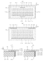
- the through-type capacitor FTC As capacitors mounted on the circuit board for the purpose of removing noise and suppressing voltage fluctuations, the through-type capacitor FTC (see Patent Document 1) exemplified in FIG. 1 (A) and the LW reversal exemplified in FIG. 2 (A) are used.
- a type capacitor LWRC (see Patent Document 2) is known.
- the through-type capacitor FTC illustrated in FIG. 1A has a first external terminal ET1 and a second external terminal ET2 at both ends in the d1 direction of the rectangular parallelepiped capacitor body CE, and is located at both ends in the center in the d2 direction. It has a third external terminal ET3 and a fourth external terminal ET4.
- the capacitor body CE has a plurality of first internal electrode layers (not shown) and a plurality of second internal electrode layers (not shown) laminated via a dielectric layer (not shown), and each of the first internal electrodes. One end of the layer is connected to the first external terminal ET1 and the other end is connected to the second external terminal ET2, one end of each second internal electrode layer is connected to the third external terminal ET3, and the other end is the fourth. It is connected to the external terminal ET4.
- FIG. 1B is a diagram illustrating a pad form when the through-type capacitor FTC is mounted on a circuit board CB, where SP1 and SP2 in the figure are signal pads and GP1 and GP2 are ground pads.
- FIG. 1C is a diagram illustrating a state in which the through-type capacitor FTC is mounted on the circuit board CB, and the first external terminal ET1 and the second external terminal ET2 of the through-type capacitor FTC are on the signal pads SP1 and SP2.
- the third external terminal ET3 and the fourth external terminal ET4 are connected to the ground pads GP1 and GP2, respectively.
- the LW reversing type capacitor LWRC illustrated in FIG. 2A has a first external terminal ET1 and a second external terminal ET2 at both ends in the d1 direction of the rectangular parallelepiped capacitor body CE, and d1 of the capacitor body CE.
- the dimension in the direction is smaller than the dimension in the d2 direction.
- the capacitor body CE has a plurality of first internal electrode layers (not shown) and a plurality of second internal electrode layers (not shown) laminated via a dielectric layer (not shown), and each of the first internal electrodes. One end of the layer is connected to the first external terminal ET1, and one end of each second internal electrode layer is connected to the second external terminal ET2.
- FIG. 2B is a diagram illustrating a pad form when the LW reversing type capacitor LWRC is mounted on a circuit board CB, where SP in the figure is a signal pad and GP is a ground pad.
- FIG. 2C is a diagram illustrating a state in which the LW reversing capacitor LWRC is mounted on the circuit board CB, and the first external terminal ET1 of the LW reversing capacitor LWRC is connected to the signal pad SP and is connected to the second external.
- the terminal ET2 is connected to the ground pad GP.
- a large number of capacitors are mounted on a circuit board for the purpose of noise removal and voltage fluctuation suppression.
- a penetration type capacitor as illustrated in FIG. 1 (A) and an LW reversal type capacitor as illustrated in FIG. 2 (A) are used together in this capacitor, and the penetration type and capacitance are the same.
- a type capacitor and an LW inverting type capacitor are used together.
- the penetration type capacitor and the LW reversal type capacitor are capacitors having different numbers and positions of external terminals, so even if the same size and capacitance are used together, the penetration type capacitor is used.
- Capacitors and LW inverting capacitors must be prepared individually, and in cases where two or more types with the same size and capacitance are required, a through-type capacitor and an LW inverting capacitor are individually prepared for each type. In addition to complicating the storage and management of each capacitor, this complication can be an obstacle to cost reduction when obtaining an electronic component mounting circuit board on which an electronic component including a capacitor is mounted.
- the problem to be solved by the present invention is a multi-terminal capacitor that can be used as a through-type capacitor and also as an LW inverting capacitor and a manufacturing method thereof, and the multi-terminal capacitor is mounted as a through-type capacitor or an LW inverting capacitor.
- the purpose is to provide a multi-terminal capacitor mounting circuit board.
- the multi-terminal capacitor according to the present invention has a rectangular shape having a capacitance forming portion capable of forming a capacitance between the first conductor film and the second conductor film facing each other via the dielectric film.
- the capacitor body is provided, the opposite direction of the two opposing surfaces of the capacitor body is the first direction, the opposite direction of the other two opposing surfaces is the second direction, and the opposite direction of the remaining two opposing surfaces is the first direction.
- a first external terminal and a second external terminal conducting with the first conductor film and a third external terminal conducting with the second conductor film Is provided so that the capacitance formed by the capacitance forming portion by the first external terminal, the second external terminal, and the third external terminal can be taken out, and the capacitor main body is provided.
- a fourth external terminal and a fifth external terminal conducting with the first conductor film and a sixth external terminal conducting with the second conductor film are provided. It is configured so that the capacitance formed in the capacitance forming portion can be taken out by the 4 external terminals, the 5th external terminal, and the 6th external terminal.
- the method for manufacturing a multi-terminal capacitor according to the present invention is a rectangular capacitor having a capacitance forming portion capable of forming a capacitance between a first conductor film and a second conductor film facing each other via a dielectric film.
- the process of manufacturing a capacitor body for manufacturing the main body the facing direction of the two facing surfaces of the capacitor body is the first direction, the facing direction of the other two facing faces is the second direction, and the remaining two facing faces
- the facing direction is the third direction
- the first external terminal and the second external terminal conducting with the first conductor film and the third external conducting with the second conductor film are conducted on one surface of the third direction of the capacitor body.
- the terminal is manufactured so that the capacitance formed by the capacitance forming portion by the first external terminal, the second external terminal, and the third external terminal can be taken out, and the other surface of the capacitor body in the third direction.
- the fourth and fifth external terminals conducting with the first conductor film and the sixth external terminal conducting with the second conductor film are the fourth external terminal, the fifth external terminal, and the sixth external terminal. It is provided with an external terminal manufacturing step of manufacturing so that the capacitance formed in the capacitance forming portion can be taken out.
- the above-mentioned multi-terminal capacitor is mounted on the circuit board by using the first external terminal, the second external terminal, and the third external terminal. Further, the above-mentioned multi-terminal capacitor is mounted on a circuit board using the fourth external terminal, the fifth external terminal, and the sixth external terminal.
- the multi-terminal capacitor according to the present invention and the manufacturing method thereof, it is possible to provide a multi-terminal capacitor that can be used as a through-type capacitor and also as an LW inverting type capacitor. Further, according to the multi-terminal capacitor mounting circuit board according to the present invention, it is possible to provide a multi-terminal capacitor mounting circuit board in which the above-mentioned multi-terminal capacitor is mounted as a through-type capacitor or an LW inverting capacitor.
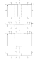
- FIG. 1 (A) to 1 (C) show a conventional penetrating capacitor, a pad form when the penetrating capacitor is mounted on the circuit board, and a state in which the penetrating capacitor is mounted on the circuit board, respectively. It is a figure which exemplifies.
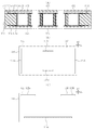
- 2 (A) to 2 (C) show the conventional LW inverting capacitor, the pad form when the same LW inverting capacitor is mounted on the circuit board, and the same LW inverting capacitor mounted on the circuit board. It is a figure which illustrates each state.
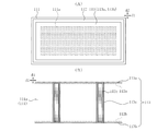
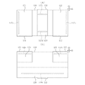
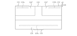
- 3 (A) is a plan view of a multi-terminal capacitor showing an application example of the present invention
- FIG. 3 (B) is a side view of the multi-terminal capacitor showing a lower side surface of FIG.
- FIG. 3 (A), and FIG. 3 (C) is a side view of the multi-terminal capacitor.
- FIG. 3 (B) is a bottom view of the multi-terminal capacitor showing the lower side surface of FIG. 3 (B)
- FIG. 3 (D) is a side view of the multi-terminal capacitor showing the lower side surface of FIG. 3 (C).
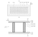
- 4 (A) is an enlarged cross-sectional view of the capacitor main body shown in FIG. 3 (A) corresponding to FIG. 3 (A)
- FIG. 4 (B) is an enlarged sectional view of the capacitor main body shown in FIG. 4 (C) is a bottom view of the capacitor body shown in FIG. 3 corresponding to FIG. 3 (C).
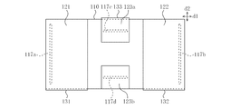
- 5 (A) is a plan view of the substrate portion shown in FIG.
- FIG. 5 (B) is a sectional view taken along line S2-S2 of FIG. 5 (A)
- FIG. (C) is explanatory drawing of the substrate part manufacturing process.
- 6 (A) and 6 (B) are explanatory views of a capacitance forming portion manufacturing step (first conductor film manufacturing step).
- 7 (A) and 7 (B) are explanatory views of a capacitance forming portion manufacturing step (dielectric film manufacturing step).
- 8 (A) and 8 (B) are explanatory views of a capacitance forming portion manufacturing step (second conductor film manufacturing step).
- 9 (A) and 9 (B) are explanatory views of the protective film manufacturing process.
- FIG. 10 (A) to 10 (D) are explanatory views of a connecting conductor portion manufacturing process.
- 11 (A) and 11 (B) are explanatory views of an external terminal manufacturing step (including a connecting conductor portion manufacturing step).
- FIG. 12 (A) shows a pad form when the multi-terminal capacitor shown in FIG. 3 is mounted on a circuit board as a through-type capacitor
- FIGS. 12 (B) and 12 (C) show the same multi-terminal capacitor.
- FIG. 12 (D) is a diagram showing a modified example of the pad form shown in FIG. 12 (A).
- FIG. 13 (A) shows a pad form when the multi-terminal capacitor shown in FIG.
- FIG. 3 is mounted on a circuit board as an LW inverting capacitor
- FIGS. 13 (B) and 13 (C) show the same multi-terminal capacitor.
- FIG. 13 (D) is a diagram showing a modified example of the pad form shown in FIG. 13 (A).
- FIG. 14 is a diagram corresponding to FIG. 3C showing a modified example of the fourth external terminal and the fifth external terminal of the multi-terminal capacitor shown in FIG.
- FIG. 15 is a diagram corresponding to FIG. 3 (A) showing a modified example of the third external terminal of the multi-terminal capacitor shown in FIG.
- the opposite direction (left-right direction in FIG. 3A) of the two opposing surfaces of the condenser body 110 described later is the “first direction d1”, and the opposite direction of the other two opposing surfaces (FIG. 3).
- the vertical direction of (A) is referred to as “second direction d2”
- the opposite direction of the remaining two opposing surfaces is referred to as “third direction d3”
- figures other than FIG. 3 (B) are also indicated in the same direction as these directions.
- the dimension along the first direction d1 of each component is "first direction dimension D1 [sign of component]”
- the dimension along the second direction d2 is “second direction dimension D2 [sign of component]”.
- the dimension along the third direction d3 is referred to as “third direction dimension D3 [sign of component]”.
- the first conductor film 112, the dielectric film 113, the second conductor film 114, the first protective layer 115, the second protective layer 116, and the first external terminals 121 to the sixth external terminals 126 which will be described later.
- the term “thickness" is used together in order to promote understanding.
- the numerical values illustrated as each dimension mean the reference dimension in design and do not include the dimensional tolerance in manufacturing.
- the multi-terminal capacitor 100 includes a rectangular parallelepiped capacitor body 110 and a first capacitor body 100 provided on one surface (upper surface of FIG. 3B) in the third direction d3.
- the external terminal 125 and the sixth external terminal 126, the first connecting conductor portion 131 connecting the first external terminal 121 and the fourth external terminal 124, and the second external terminal 122 and the fifth external terminal 125 are connected.
- a second connecting conductor portion 132 is provided, and a third connecting conductor portion 133 that connects the third external terminal 123 and the sixth external terminal 126 is provided.
- the first direction dimension D1 [110] of the capacitor body 110 is larger than the second direction dimension D2 [110], and the third direction dimension D3 [110] is. It is smaller than the second direction dimension D2 [110].
- the numerical values of the first direction dimension D1 [110], the second direction dimension D2 [110], and the third direction dimension D3 [110] are the relationship of the first direction dimension D1 [110]> the second direction dimension D2 [110], or In addition to this, there is no particular limitation as long as the relationship of the third direction dimension D3 [110] ⁇ second direction dimension D2 [110] is satisfied.
- the first direction dimension D1 [110] of the capacitor body 110 can be exemplified in the range of 400 to 1600 ⁇ m, and the second direction dimension D2 [110] can be in the range of 200 to 800 ⁇ m.
- the second direction dimension D2 [110] can be 100 ⁇ m or less, or 50 ⁇ m or less.
- the capacitor main body 110 includes: a rectangular substrate portion 111 having a plurality of through holes 111a (see FIGS. 4A, 5A and 5B), and a first substrate portion 111.
- a first conductor film 112 that continuously covers one surface of the three-direction d3 (upper surface of FIG. 4A), the other surface of the third direction d3 (lower surface of FIG. 4A), and the inner wall of each through hole 111a. (See FIGS. 4 (A) and 6),: The dielectric film 113 covering the first conductor film 112 (see FIGS. 4 (A) and 7), and the second conductor covering the dielectric film 113.
- Capacitance can be formed between the first conductor film 112 and the second conductor film 113 which have a film 114 (see FIGS. 4A and 8) and face each other via the dielectric film 113.
- a capacitance forming unit (reference numeral omitted) is configured.
- the first direction dimension D1 [111] of the substrate portion 111 is larger than the second direction dimension D2 [111], and the third direction dimension D3 [111] ] Is smaller than the second direction dimension D2 [111].
- each through hole 111a is a tetragonal column whose first direction dimension D1 [111a] is larger than that of the second direction dimension D2 [111a], the total number of through holes 111a is 105, and the arrangement of the through holes 111a is It is a grid array with 7 first directions d1 and 15 second directions d2, and the intervals of the through holes 111a arranged in the first direction d1 are the same, and the intervals of the through holes 111a arranged in the second direction d2 are also the same.
- the numerical ranges of the first-direction dimension D1 [111], the second-direction dimension D2 [111], and the third-direction dimension D3 [111] of the substrate portion 111 are the above-mentioned capacitors. It suffices as long as it conforms to each numerical range of the first direction dimension D1 [110], the second direction dimension D2 [110], and the third direction dimension D3 [110] of the main body 110.
- first direction dimension D1 [111a] of the through hole 111a can be exemplified in the range of 5 to 20 ⁇ m
- second direction dimension D2 [111a] can be exemplified in the range of 0.5 to 2 ⁇ m
- first direction d1 can be exemplified.
- the distance between the through holes 111a arranged in the same direction can be exemplified in the range of 1 to 10 ⁇ m
- the distance between the through holes 111a arranged in the second direction d2 can be exemplified in the range of 0.5 to 2 ⁇ m.
- the tetragonal columnar through hole 111a has been illustrated, it can be changed to a pentagonal columnar shape, a columnar shape, an elliptical columnar shape, or the like if the same capacitance as described later can be formed. Further, although a plurality of through holes 111a arranged in a grid pattern is illustrated, it can be changed to a staggered arrangement or the like if the same capacitance as described later can be formed.
- the first conductor film 112 includes a rectangular first planar portion 112a (see FIG. 6B) on one surface (upper surface of FIG. 4A) of the substrate portion 111 in the third direction d3.
- the dielectric film 113 includes a rectangular first planar portion 113a (see FIG. 7B) on one surface (upper surface of FIG. 4A) of the substrate portion 111 in the third direction d3 and a substrate.
- the second conductor film 114 includes a rectangular first planar portion 114a (see FIG. 8B) located on one surface (upper surface of FIG. 4A) of the substrate portion 111 in the third direction d3.
- the directional dimension D1 [112a & 112b] is larger than the second directional dimension D2 [112a & 112b], and the first directional dimension D1 [112a & 112b] is smaller than the first directional dimension D1 [111] of the substrate portion 111.
- [112a & 112b] is smaller than the second direction dimension D2 [111] of the substrate portion 111.
- the first-direction dimension D1 [113a & 113b] of the first planar portion 113a and the second planar portion 113b of the dielectric film 113 is larger than the second-direction dimension D2 [113a & 113b], and the first-direction dimension D1 [113a & 113b].
- the second direction dimension D2 [113a & 113b] is the first surface of the first conductor film 112. It is smaller than the second direction dimension D2 [112a & 112b] of the shaped portion 112a and the second planar portion 112b.
- the first-direction dimensions D1 [114a & 114b] of the first planar portion 114a and the second planar portion 114b of the second conductor film 114 are larger than the second-direction dimensions D2 [114a & 114b], and the first-direction dimensions D1 [114a & 114b].
- the first-direction dimensions D1 [112a & 112b] and the second-direction dimensions D2 [112a & 112b] of the first planar portion 112a and the second planar portion 112b of the first conductor film 112 are The first directional dimensions D1 [113a & 113b] and the second directional dimensions D2 [113a & 113b] of the first planar portion 113a and the second planar portion 113b of the dielectric film 113, and the first planar portion 114a of the second conductor film 114.
- the numerical ranges of the first-direction dimensions D1 [114a & 114b] and the second-direction dimensions D2 [114a & 114b] of the second planar portion 114b satisfy the above-mentioned relationship and are the first-direction dimensions of the above-mentioned capacitor body 110. There is no particular limitation as long as it is within the numerical range of D1 [110] and the second direction dimension D2 [110]. Further, the thickness of the first conductor film 112, the thickness of the dielectric film 113, and the thickness of the second conductor film 113 can be exemplified in the range of 1 to 500 nm.
- the capacitance forming portion (reference numeral omitted) is dielectric with the first planar portion 112a of the first conductor film 112 located on one surface (upper surface of FIG. 4A) of the third direction d3 of the substrate portion 111.
- the partial capacitance that can be formed by the first planar portion 113a of the body film 113 and the first planar portion 114a of the second conductor film 114, and the other surface of the substrate portion 111 in the third direction d3 (FIG. 4 (A). ), Which can be formed by the second planar portion 112b of the first conductor film 112, the second planar portion 113b of the dielectric film 113, and the second planar portion 114b of the third conductor film 114.
- the above-mentioned capacitance can be formed by the partial capacitance that can be formed.
- the capacitor main body 110 includes: -A first conductor film 112, a dielectric film 113, and a second conductor film 114, respectively, located on one surface (upper surface of FIG. 4A) of the substrate portion 111 in the third direction d3.
- the first protective film 115 (see FIGS. 4A and 9A) that covers the one-sided portions 112a, 113a and 114a, and the other surface of the substrate portion 111 in the third direction d3 (FIG. 4).
- the second protective film 116 (FIG. 4 (FIG.
- the first protective film 115 has the first-direction dimension D1 [115] and the second-direction dimension D2 [115], and the second protective film 116.
- the first-direction dimension D1 [116] and the second-direction dimension D2 [116] of the above are the same as or substantially the same as the first-direction dimension D1 [111] and the second-direction dimension D2 [111] of the substrate portion 111.
- the first-direction dimension D1 [115] and the second-direction dimension D2 [115] of the first protective film 115 and the first-direction dimension D1 [116] of the second protective film 116 may be compatible with the numerical range of the first direction dimension D1 [110] and the second direction dimension D2 [110] of the capacitor body 110 described above.
- the thickness of the first protective film 115 and the thickness of the second protective film 116 can be exemplified in the range of 0.2 to 5 ⁇ m.
- the first connecting conductor portion 117a is one end portion of the first protective film 115 in the first direction d1 (in FIG. 10A).
- the left end portion is provided so as to penetrate the third direction d3 and to be in contact with one end portion (left end portion in FIG. 10A) of the first planar portion 112a of the first conductor film 112 in the first direction d1.
- the first direction dimension D1 [117a] is smaller than the second direction dimension D2 [117a]
- the second direction dimension D2 [117a] is the second of the first planar portion 112a of the first conductor film 112. It is slightly smaller than the directional dimension D2 [112a].
- the second connecting conductor portion 117b penetrates the other end of the first protective film 115 in the first direction d1 (the right end portion in FIG. 10A) in the third direction d3, and is formed by the first conductor film 112. It is provided so as to be in contact with the other end of the first planar portion 112a (the right end portion in FIG. 10A), and the first direction dimension D1 [117b] is the second direction dimension D2 [117b]. ], And the second direction dimension D2 [117b] is slightly smaller than the second direction dimension D2 [112a] of the first planar portion 112a of the first conductor film 112.
- the third connecting conductor portion 117c penetrates the center of one end portion of the first protective film 115 in the first direction d1 (the center in the left-right direction of the upper end portion of FIG. 10A) in the third direction d3, and is third.
- the two conductor film 114 is provided so as to be in contact with the center of the first direction d1 of one end of the first planar portion 114a (the center in the left-right direction of the upper end portion of FIG. 10A), and the first direction dimension D1 thereof.
- [117c] is larger than the second direction dimension D2 [117c]
- the first direction dimension D1 [117c] is slightly smaller than the first direction dimension D1 [123] of the third external terminal 123.
- the fourth connecting conductor portion 117d penetrates the center of the other end of the first protective film 115 in the first direction d1 (the center of the lower end of FIG. 10A in the left-right direction) in the third direction d3.
- the second conductor film 114 is provided so as to be in contact with the center of the first direction d1 of the other end of the first planar portion 114a (the center of the lower end of FIG. 10A in the left-right direction), and the first direction thereof.
- the dimension D1 [117d] is larger than the second direction dimension D2 [11dc], and the first direction dimension D1 [117d] is slightly smaller than the first direction dimension D1 [123] of the third external terminal 123.
- the connection resistance between the first conductor film 112 and the first external terminal 121 or the second external terminal 122 does not increase in the first connecting conductor portion 117a and the second connecting conductor portion 117b.
- the third connecting conductor portion 117c and the fourth connecting conductor portion 117d have dimensions D1 [117c & 117d] in the first direction and the second direction so that the connection resistance between the second conductor film 114 and the third external terminal 123 does not increase.
- the dimension D2 [117c & 117d] is the same as or slightly larger than the thickness of the first protective film 115.
- the fifth connecting conductor portion 118a to the seventh connecting conductor portion 118c will be described with reference to FIG. 10.
- the fifth connecting conductor portion 118a is one of the first directions d1 of one end of the second direction d2 of the second protective film 116.
- the first direction d1 of one end of the second plane portion 112b of the first conductor film 112 and the second direction d2 so as to penetrate the side (the left side of the upper end portion of FIG. 10B) in the third direction d3. It is provided so as to be in contact with one side (the left side of the upper end portion of FIG. 10B), and its first direction dimension D1 [118a] is larger than the second direction dimension D2 [118a] and is larger than the second direction dimension D2 [118a].
- D1 [118a] is slightly smaller than the first direction dimension D1 [124] of the fourth external terminal 124.
- the sixth connecting conductor portion 118b penetrates the other side of the first direction d1 (the right side of the upper end portion of FIG. 10B) in the third direction d3 at one end of the second direction d2 of the second protective film 116.
- the second planar portion 112b of the first conductor film 112 is provided so as to be in contact with the other side of the first direction d1 (the right side of the upper end portion in FIG. 10B) at one end of the second direction d2.
- the first direction dimension D1 [118b] is larger than the second direction dimension D2 [118b]
- the first direction dimension D1 [118b] is slightly larger than the first direction dimension D1 [125] of the fifth external terminal 125. Is small.
- the seventh connecting conductor portion 118c penetrates the other end portion (lower end portion of FIG. 10B) of the second protective film 116 in the second direction d2 in the third direction d3, and is formed by the second conductor film 114. It is provided so as to be in contact with one end of the second planar portion 114b (the lower end of FIG. 10B), and the first direction dimension D1 [118c] is larger than the second direction dimension D2 [118c].
- the first-direction dimension D1 [118b] is slightly smaller than the first-direction dimension D1 [114b] of the second planar portion 114b of the second conductor film 114.
- the connection resistance between the first conductor film 112 and the fourth external terminal 124 or the fifth external terminal 125 does not increase in the fifth connecting conductor portion 118a and the sixth connecting conductor portion 117b.
- the seventh connecting conductor portion 118c can have the first direction dimension D1 [118c] and the second direction dimension D2 [118c] so that the connection resistance between the second conductor film 112 and the sixth external terminal 126 does not increase. It is preferable to take as large as possible.
- the third direction dimension D3 [118a to 118c] of the fifth connecting conductor portion 118a to the seventh connecting conductor portion 118c is the same as or slightly larger than the thickness of the second protective film 116.
- the first external terminal 121 has a rectangular shape, and one surface of the capacitor main body 110 in the third direction d3. It exists at one end of the first direction d1 (the left end of FIG. 3A), and its first direction dimension D1 [121] is smaller than 1/2 of the first direction dimension D1 [110] of the capacitor body 110.
- the second direction dimension D2 [121] is the same as or substantially the same as the second direction dimension D2 [110] of the capacitor body 110.
- the second external terminal 122 has a rectangular shape, and the first external terminal 121 is located at the other end of the first direction d1 (right end in FIG. 3A) on one surface of the third direction d3 of the capacitor main body 110.
- the first direction dimension D1 [122] is smaller than 1/2 of the first direction dimension D1 [110] of the capacitor main body 110, and the second direction dimension D2 [121] is separated from the first direction d1. Is the same as or almost the same as the second direction dimension D2 [110] of the capacitor body 110.
- the first direction dimension D1 [122] and the second direction dimension D2 [122] of the second external terminal 122 are the first direction dimension D1 [121] and the second direction dimension D2 of the first external terminal 121. The same thing as [121] is drawn.
- the third external terminal 123 has a rectangular shape, and is between the first external terminal 121 and the second external terminal 121 on one surface of the third direction d3 of the capacitor main body 110 (center in the left-right direction in FIG. 3A). ) Exists in non-contact with the first external terminal 121 and the second external terminal 122, the first direction dimension D1 [123] of which is smaller than the second direction dimension D2 [123], and the second direction dimension D2 [123]. Is the same as or almost the same as the second direction dimension D2 [110] of the capacitor body 110.
- the first external terminal 121, the second external terminal 122, and the third external terminal 123 have first-direction dimensions D1 [121 to 123] and second-direction dimensions D2 [121 to 123]. Is preferably made as large as possible so that the connection resistance when mounted on the circuit board 200 described later does not increase. However, the distance between the first external terminal 121 and the third external terminal 123 (the distance between the first direction d1) and the distance between the second external terminal 122 and the third external terminal 123 (the distance between the first direction d1) are different. It is preferably 100 ⁇ m or more in order to prevent a short circuit due to the bonding material used when mounting on the circuit board 200 described later. Further, the thickness of the first external terminal 121, the thickness of the second external terminal 122, and the thickness of the third external terminal 123 can be exemplified in the range of 5 to 10 ⁇ m.
- the fourth external terminal 124 has a rectangular shape, and the second direction d2 on the other side of the third direction d3 of the capacitor main body 110. It exists on one side of one end of the above (left side of the upper end of FIG. 3C), and its first direction dimension D1 [124] is the same as or almost the same as the first direction dimension D1 [121] of the first external terminal 121. It is the same, and the second direction dimension D2 [124] is smaller than 1/2 of the second direction dimension D2 [110] of the capacitor body 110.
- the fifth external terminal 125 has a rectangular shape and exists on the other side of one end of the second direction d2 on the other side of the third direction d3 of the capacitor body 110 (on the right side of the upper end portion in FIG. 3C).
- the first direction dimension D1 [125] is the same as or almost the same as the first direction dimension D1 [122] of the second external terminal 122
- the second direction dimension D2 [125] is the second direction of the capacitor body 110. It is smaller than 1/2 of the dimension D2 [110].
- the sixth external terminal 126 has a rectangular shape, exists at the other end of the second direction d2 (the lower end of FIG. 3C) on the other side of the third direction d3 of the capacitor main body 110, and is the third.
- the one-way dimension D1 [126] is the same as or almost the same as the first-direction dimension D1 [110] of the capacitor body 110, and the second-direction dimension D2 [126] is the second-direction dimension D2 [110] of the capacitor body 110. Less than 1/2.
- the first-direction dimensions D1 [121 to 123] and the second-direction dimensions D2 [121 to 123] of the fourth external terminal 124, the fifth external terminal 125, and the sixth external terminal 126 Is preferably made as large as possible so that the connection resistance when mounted on the circuit board 200 described later does not increase.
- the distance between the 4th external terminal 124 and the 5th external terminal 125 (distance in the first direction d1) and the distance between the 4th external terminal 124 and the 5th external terminal 125 and the 6th external terminal 126 (second direction).
- the interval (d2) is preferably 100 ⁇ m or more in order to prevent a short circuit due to the bonding material used when mounting on the circuit board 200 described later. Further, the thickness of the fourth external terminal 124, the thickness of the fifth external terminal 125, and the thickness of the sixth external terminal 126 can be exemplified in the range of 5 to 10 ⁇ m.
- the first external terminal 121, the second external terminal 122, and the third external terminal provided on one surface of the capacitor main body 110 in the third direction d3 can be taken out by the capacitor 123, and the other surface of the capacitor body 110 in the third direction d3 (lower surface of FIG. 3B, FIG. 3).
- the fourth external terminal 124, the fifth external terminal 125, and the sixth external terminal 126 provided in (see (C)) can also take out the capacitance formed by the capacitance forming portion (reference numeral omitted). It has become.
- the first connecting conductor portion 131 has a rectangular shape, and one end edge in the third direction d3 ( The upper edge of FIG. 3B is continuous with one end edge of the first external terminal 121 in the second direction d2 (lower edge of FIG. 3A), and the other end edge of the third direction d3 (FIG. 3B). ) Is continuous with one end edge (upper edge of FIG. 3C) of the fourth external terminal 124 in the second direction d2, and the first direction dimension D1 [131] is the first edge of the first external terminal 121. It is the same as or substantially the same as the one-way dimension D1 [121] and the first-way dimension D1 [124] of the fourth external terminal 124.
- the second connecting conductor portion 132 has a rectangular shape, and one end edge of the third direction d3 (upper edge of FIG. 3B) is one end edge of the second external terminal 122 in the second direction d2 (FIG. 3 (FIG. 3).
- the other end edge (lower edge of FIG. 3B) of the third direction d3 is continuous with the lower edge of A), and the one end edge of the fifth external terminal 125 in the second direction d2 (upper edge of FIG. 3C).
- its first directional dimension D1 [132] is the same as or almost the same as the first directional dimension D1 [122] of the second external terminal 122 and the first directional dimension D1 [125] of the fifth external terminal 125. Is.
- the third connecting conductor portion 133 has a rectangular shape, and one end edge of the third direction d3 (lower edge of FIG. 3D) is one end edge of the third external terminal 123 in the second direction d2 (FIG. 3 (FIG. 3).
- the other end edge (upper edge of FIG. 3D) of the third direction d3 is continuous with the upper edge of A) and is the center of the first direction d1 of the one end edge of the second direction d2 of the sixth external terminal 123. It is continuous with the lower edge in FIG. 3C (center in the left-right direction), and its first-direction dimension D1 [133] is the same as or substantially the same as the first-direction dimension D1 [123] of the third external terminal 123.
- the first connecting conductor portion 131 can have its first dimension D1 [131] so that the connecting resistance between the first external terminal 121 and the fourth external terminal 124 does not increase. It is preferable to make the second connecting conductor portion 132 as large as possible, and the first direction dimension D1 [132] of the second connecting conductor portion 132 is made as large as possible so that the connecting resistance between the second external terminal 122 and the fifth external terminal 125 does not increase. It is preferable that the third connecting conductor portion 133 has its first direction dimension D1 [133] as large as possible so that the connecting resistance between the third external terminal 123 and the sixth external terminal 126 does not increase. preferable. Further, the thickness of the first connecting conductor portion 131 child 121, the thickness of the second external terminal 122, and the thickness of the third external terminal 123 can be exemplified in the range of 5 to 10 ⁇ m.
- the other surface of the first external terminal 121 and the third direction d3 provided on one surface of the capacitor main body 110 in the third direction d3 see the upper surface of FIG. 3B and FIG. 3A) (FIG. 3).
- the lower surface of (B) and the fourth external terminal 124 provided in FIG. 3 (C) are connected by the first connecting conductor portion 131, and one surface of the capacitor main body 110 in the third direction d3 (FIG. 3 (FIG. 3).
- the upper surface of B) is provided on the second external terminal 122 provided in FIG. 3 (A) and the other surface of the third direction d3 (lower surface of FIG. 3 (B), see FIG. 3 (C)).
- the fifth external terminal 125 is connected by the second connecting conductor portion 132, and is provided on one surface of the capacitor main body 110 in the third direction d3 (see the upper surface of FIG. 3B and FIG. 3A).
- the third external terminal 123 and the sixth external terminal 125 provided on the other surface of the third direction d3 (lower surface of FIG. 3B, see FIG. 3C) are connected by the third connecting conductor portion 133.
- FIGS. 6 to 11 a method of manufacturing the above-mentioned multi-terminal capacitor 100 will be described with reference to FIGS. 6 to 11.
- the drawings corresponding to one multi-terminal capacitor 100 are drawn in FIGS. 6 to 11, in reality, a large number of capacitors that are divided into desired sizes are adopted after the connection conductor portion manufacturing step described later.
- the manufacturing method of the multi-terminal capacitor 100 is as follows: -Substrate part manufacturing process, -Capacity forming part manufacturing process, -Protective film manufacturing process, -Connecting conductor manufacturing process, -External terminal manufacturing process (Connecting conductor manufacturing process) Includes) and
- Substrate Part Fabrication Step In the step of manufacturing the substrate portion 111, as illustrated in FIGS. 5 (A) to 5 (C), a base material P111 having a thickness larger than that of the substrate portion 111 is prepared, and the base material P111 is prepared. An etching mask (not shown) corresponding to the through hole 111a is formed on one surface (upper surface of FIG. 5C) of the material P111 in the third direction d3, and a deep groove P111a is formed in the base material P111 by etching using this etching mask. After the etching mask is formed, the etching mask is removed, and the other surface of the base material P111 in the third direction d3 is partially removed (the portion below the line RL in FIG. 5C) by grinding or the like. This is done by obtaining the substrate portion 111 illustrated in 5 (A) and 5 (B).
- CMOS complementary metal-oxide-semiconductor
- CMOS complementary metal-oxide-semiconductor
- DRIE deep etching method
- the step of manufacturing the capacitance forming portion is one of the third directions d3 of the substrate portion 111, as illustrated in (1) FIGS. 6 (A) and 6 (B).
- the materials of the first conductor film 112 and the second conductor film 114 include known conductors such as nickel, copper, palladium, platinum, silver, gold, ruthenium, tungsten, molybdenum, titanium or metals such as alloys thereof. Conductive materials such as conductive silicone can be used, and among them, titanium (titanium nitride) is preferable.
- the methods for producing the first conductor film 112, the dielectric film 113, and the second conductor film 114 include a known dry plating method and a wet plating method, for example, a sputtering method, a vapor deposition method, and an atomic layer volume method (ALD method). A method, an electrolytic plating method, a electroless plating method and the like can be used, and among them, the atomic layer volume method (ALD method) is preferable.
- the steps for manufacturing the first protective film 115 and the second protective film 116 are as follows: (1) Third direction d3 of the substrate portion 111. A first protective film that covers the first planar portions 112a, 113a, and 114a of the first conductor film 112, the dielectric film 113, and the second conductor film 114 on one surface (upper surface of FIG. 9B), respectively. The step of producing 115, and (2) the first conductor film 112, the dielectric film 113, and the second conductor film 114 on the other surface (lower surface of FIG. 9B) of the substrate portion 111 in the third direction d3, respectively. Includes a step of making a second protective film 116 that covers the second planar portions 112b, 113b and 114b of the above.
- Known insulators such as polyimide, silicon oxide, silicon nitride, silicon oxynitride and the like can be used as the material of the first protective film 115 and the second protective film 116, and silicon nitride is preferable among them.
- known film forming methods such as a spin coating method, a spray coating method, and a printing method can be used, and among them, the spin coating method is preferable.
- a barrier film for preventing the invasion of water, hydrogen, etc. into the capacitance forming portion may be formed between the capacitance forming portion (reference numeral omitted) and the protective films 115 and 116.
- the thickness of the barrier film can be exemplified in the range of 5 to 500 nm, and known insulators such as alumina, zirconia, silicon oxide, silicon oxynitride and the like can be used as the material of the barrier film, and as a manufacturing method. Can be used by a sputtering method, a CVD method, or the like.
- FIGS. 10A to 10D The steps of manufacturing the first connecting conductor portion 117a to the fourth connecting conductor portion 117d and the fifth connecting conductor portion 118a to the seventh connecting conductor portion 118c are shown in FIGS. 10A to 10D. ), An etching mask corresponding to the first connecting conductor portion 117a to the fourth connecting conductor portion 117d on one surface (upper surface of FIG. 10D) of the first protective film 115 in the third direction d3 (not shown). ) Is formed, a through hole TH is formed in the first protective film 115 by etching using this etching mask (see FIG. 10C), and then the etching mask is removed and the through hole TH is formed. A conductor portion CP is produced (see FIG.
- an etching mask (illustrated) corresponding to the fifth connecting conductor portion 118a to the seventh connecting conductor portion 118c on one surface (the surface appearing in FIG. 10B) of the second protective film 116 in the third direction d3. (Omitted) is formed, a through hole TH (not shown) is formed in the second protective film 116 by etching using this etching mask, and then the etching mask is removed, and the conductor portion CP (not shown) is formed in each through hole TH. (Not shown) is produced.
- a known dry etching method and a wet etching method can be selectively used as the etching method, and the dry etching method is particularly preferable.
- a known conductor for example, a metal such as copper, nickel, tin, palladium, platinum, gold or an alloy thereof can be used, and nickel is preferable among them.
- Known dry plating methods and wet plating methods for example, a sputtering method, a vapor deposition method, an electrolytic plating method, an electroless plating method, and the like can be used as a method for producing the conductor portion CP, and the electroless plating method is preferable.
- the external terminal manufacturing process includes the first external terminal 121 to the sixth external terminal 122 and the first connecting conductor portion 131 to the third connection. It differs depending on whether the conductor portion 133 is composed of a single film or a plurality of films. When these are made of a single film, as shown in FIGS. 11 (A) and 11 (B), the first external terminal 121 to the sixth terminal 122 and the first connection are first formed on the entire surface of the capacitor body 110.
- a plating mask is formed on the portion where the conductor portion 131 to the third connecting conductor portion 133 is not manufactured, and the first external terminal 121 to the sixth terminal 122 and the first connecting conductor portion 131 to the third connecting are formed by plating using this plating mask.
- the conductor portion 133 is manufactured, and the plating mask after the fabrication is removed.
- Known conductors such as titanium, copper, nickel, silver, gold, platinum, palladium, tin, chrome, titanium, tantalum, tungsten, molybdenum or alloys thereof can be used as the material for the single film, among which titanium.
- nickel is preferred.
- a known dry plating method for example, a sputtering method, a vapor deposition method, a CVD method, or the like can be used as a method for producing a single film, and the sputtering method is preferable.
- a known baking method that is, a method in which a conductor paste is applied by roller coating, printing, or the like and baked.
- the single film is used as a base film and a second film is formed on the surface thereof.
- the material after the second film is used as the single film. It may be different. Taking the case where the number of films is 4, a combination in which the first film (the single film) is titanium, the second film is nickel, the third film is copper, and the fourth film is tin. , A combination in which the first film (the single film) is nickel, the second film is copper, the third film is nickel, and the fourth film is tin can be exemplified. Of course, combinations other than these may be adopted.
- a known wet plating method for example, an electrolytic plating method, an electroless plating method, or the like can be used as a method for producing the second and subsequent films, and the electrolytic plating method is preferable.
- a known baking method that is, a method of applying a conductor paste by roller coating, printing, or the like and baking the second or subsequent film.
- FIG. 12A is a diagram illustrating a pad form when the multi-terminal capacitor 100 is mounted on the circuit board 200 as a through-type capacitor, in which 201 and 202 are signal pads and 203 and 204 are ground pads.
- .. 12 (B) and 12 (C) are diagrams and connection explanatory views showing a state in which the multi-terminal capacitor 100 is mounted on the circuit board 200 as a through-type capacitor, and the multi-terminal capacitor 100 solders the first external terminal 121.
- the second external terminal 122 is connected to the signal pad 202 using the same bonding material, and the third external terminal 123 is connected to the ground using the same bonding material. It is connected to pads 203 and 204.
- FIG. 12 (D) is a diagram illustrating a pad form that is a substitute for the pad form illustrated in FIG. 12 (A). In this pad form, two ground pads 203 and 204 are used as one ground pad 203'. It is configured.
- FIG. 13A is a diagram illustrating a pad form when the multi-terminal capacitor 100 is mounted on the circuit board 200 as an LW inverting capacitor, where 211 in the figure is a signal pad and 212 is a ground pad.
- 13 (B) and 13 (C) are diagrams and connection explanatory views showing a state in which the multi-terminal capacitor 100 is mounted on the circuit board 200 as an LW inverting capacitor, and the multi-terminal capacitor 100 includes the fourth external terminal 124 and The fifth external terminal 125 is connected to the signal pad 211 using a bonding material such as solder (not shown), and the sixth external terminal 126 is connected to the ground pad 212 using the same bonding material.
- FIG. 13 (B) and 13 (C) are diagrams and connection explanatory views showing a state in which the multi-terminal capacitor 100 is mounted on the circuit board 200 as an LW inverting capacitor, and the multi-terminal capacitor 100 includes the fourth external terminal 124 and The fifth external terminal 125 is connected to the signal pad 211
- FIG. 13 (D) is a diagram illustrating a pad form that is a substitute for the pad form illustrated in FIG. 13 (A).
- one signal pad 211 is the fourth external terminal of the multi-terminal capacitor 100. It is divided into two signal pads 211'according to 124 and the fifth external terminal 125.
- the multi-terminal capacitor 100 is a first external terminal 121 provided on one surface of the third direction d3 of the capacitor body 110 (see the upper surface of FIG. 3B and FIG. 3A).
- the second external terminal 122 and the third external terminal 123 allow the capacitance formed by the capacitance forming portion (reference numeral omitted) to be taken out, and the other surface of the capacitor body 110 in the third direction d3.
- the capacitance forming portion (reference numeral omitted) is also formed by the fourth external terminal 124, the fifth external terminal 125, and the sixth external terminal 126 provided on the lower surface of FIG. 3B, see FIG. 3C). It is possible to take out the capacitance formed by.
- a penetrating capacitor 100 can be used as a penetrating capacitor and also as an LW reversing capacitor, a penetrating capacitor can be used in the case where the same size and capacitance are used together as in the past.
- LW inverting capacitors do not need to be prepared individually, and even if two or more types with the same size and capacitance are required, it is necessary to prepare through-type capacitors and LW inverting capacitors individually for each type. Absent.
- the first conductor film 112, the dielectric film 113, and the second conductor film 114 are used one by one, but the dielectric film covering the second conductor film and the third covering the dielectric film are shown. It is also possible to add a conductor film to form a capacitance forming portion (reference numeral omitted), and further add a dielectric film covering the third conductor film and a fourth conductor film covering the dielectric film. It is also possible to configure the capacitance forming unit (reference numeral omitted) by the above.
- the first direction dimension D1 [121] of the first external terminal 121 and the first direction dimension D1 [124] of the fourth external terminal 124 are the same or almost the same, and the first direction dimension D1 of the second external terminal 122. [122] and the first direction dimension D1 [125] of the fifth external terminal 125 are the same as or almost the same, but as illustrated in FIG. 14, the first direction dimension D1 [12'of the fourth external terminal 124'[ 124'] is made larger than the first direction dimension D1 [121] of the first external terminal 121, and the first direction dimension D1 [125'] of the fifth external terminal 125'is the first direction dimension of the second external terminal 122.
- the mounting area (connection area) of the fourth external terminal 124'and the fifth external terminal 125' may be increased by making it larger than D1 [121].
- FIG. 15 An example in which the third connecting conductor portion 117c and the fourth connecting conductor portion 117d are connected to the third external terminal 123 is illustrated, but as illustrated in FIG. 15, the third external terminal 123 is divided into the first division.
- a second divided portion 123b is composed of a portion 123a, the first divided portion 123a, and a second divided portion 123b separated in the second direction d2, and a third connecting conductor portion 117c is connected to the first divided portion 123a.
- the fourth connecting conductor portion 117d may be connected to.
- the first division portion 123a may be connected to the sixth external terminal 126 by the third connecting conductor portion 133.
- Multi-terminal capacitor, 110 Condenser body, 111 ... Substrate, 111a ... Through hole, 112 ... First conductor film, 112a ... First surface, 112b ... Second surface, 112c ... Cylindrical, 113 ... Dielectric film, 113a ... First planar portion, 113b ... Second planar portion, 113c ... Cylindrical portion, 114 ... Second conductor film, 114a ... First planar portion, 114b ... Second planar portion , 114c ... Cylindrical part, 115 ... First protective film, 116 ... Second protective film, 117a ... First connecting conductor part, 117b ...
Landscapes
- Engineering & Computer Science (AREA)
- Power Engineering (AREA)
- Microelectronics & Electronic Packaging (AREA)
- Manufacturing & Machinery (AREA)
- Chemical & Material Sciences (AREA)
- Ceramic Engineering (AREA)
- Inorganic Chemistry (AREA)
- Fixed Capacitors And Capacitor Manufacturing Machines (AREA)
- Structures For Mounting Electric Components On Printed Circuit Boards (AREA)
- Ceramic Capacitors (AREA)
Abstract
【課題】貫通型コンデンサとして使用できるとともにLW逆転型コンデンサとしても使用できる多端子コンデンサを提供する。【解決手段】多端子コンデンサ100は、誘電体膜113を介して向き合う第1導体膜112と第2導体膜114との間で静電容量を形成し得る容量形成部を有する直方体状のコンデンサ本体110を備える。また、コンデンサ本体110の第3方向d3の一方面には、第1導体膜112と導通する第1外部端子121および第2外部端子122と、第2導体膜114と導通する第3外部端子123とが設けられ、コンデンサ本体110の第3方向d3の他方面には、第1導体膜112と導通する第4外部端子124および第5外部端子125と、第2導体膜114と導通する第6外部端子126とが設けられている。
Description
本発明は、多端子コンデンサおよびその製造方法と、当該多端子コンデンサが回路基板に実装された多端子コンデンサ実装回路基板に関する。
ノイズ除去や電圧変動抑制等を目的とし回路基板に実装されるコンデンサとして、図1(A)に例示した貫通型コンデンサFTC(特許文献1を参照)と、図2(A)に例示したLW逆転型コンデンサLWRC(特許文献2を参照)が知られている。
図1(A)に例示した貫通型コンデンサFTCは、直方体状のコンデンサ本体CEのd1方向の両端部に第1外部端子ET1と第2外部端子ET2を有し、d2方向の中央の両端部に第3外部端子ET3と第4外部端子ET4を有する。コンデンサ本体CEは誘電体層(図示省略)を介して積層された複数の第1内部電極層(図示省略)と複数の第2内部電極層(図示省略)とを有し、各第1内部電極層の一端部は第1外部端子ET1に接続され他端部は第2外部端子ET2に接続され、各第2内部電極層の一端部は第3外部端子ET3に接続され他端部は第4外部端子ET4に接続されている。
図1(B)は前記貫通型コンデンサFTCを回路基板CBに実装するときのパッド形態を例示する図であり、同図のSP1およびSP2はシグナルパッド、GP1およびGP2はグラウンドパッドである。図1(C)は前記貫通型コンデンサFTCを前記回路基板CBに実装した状態を例示する図であり、貫通型コンデンサFTCの第1外部端子ET1および第2外部端子ET2はシグナルパッドSP1およびSP2にそれぞれ接続され、第3外部端子ET3および第4外部端子ET4はグラウンドパッドGP1およびGP2にそれぞれ接続されている。
一方、図2(A)に例示したLW逆転型コンデンサLWRCは、直方体状のコンデンサ本体CEのd1方向の両端部に第1外部端子ET1と第2外部端子ET2を有し、コンデンサ本体CEのd1方向の寸法はd2方向の寸法よりも小さい。コンデンサ本体CEは誘電体層(図示省略)を介して積層された複数の第1内部電極層(図示省略)と複数の第2内部電極層(図示省略)とを有し、各第1内部電極層の一端部は第1外部端子ET1に接続され、各第2内部電極層の一端部は第2外部端子ET2に接続されている。
図2(B)は前記LW逆転型コンデンサLWRCを回路基板CBに実装するときのパッド形態を例示する図であり、同図のSPはシグナルパッド、GPはグラウンドパッドである。図2(C)は前記LW逆転型コンデンサLWRCを前記回路基板CBに実装した状態を例示する図であり、LW逆転型コンデンサLWRCの第1外部端子ET1はシグナルパッドSPに接続され、第2外部端子ET2はグラウンドパッドGPに接続されている。
ところで、スマートフォンやノートブックコンピューター等の電子機器には、ノイズ除去や電圧変動抑制等を目的として数多くのコンデンサが回路基板に実装されている。このコンデンサには図1(A)に例示したような貫通型コンデンサと図2(A)に例示したようなLW逆転型コンデンサが併用されるケースが少なくなく、サイズおよび静電容量等が同じ貫通型コンデンサとLW逆転型コンデンサが併用されるケースも少なくない。
しかしながら、先に述べたように貫通型コンデンサとLW逆転型コンデンサは外部端子の数および位置が異なるコンデンサであるため、サイズおよび静電容量等が同じものが併用されるケースであっても貫通型コンデンサとLW逆転型コンデンサを個々に用意しなければならず、サイズおよび静電容量等が同じものが2種類以上必要なケースでは各種類毎に貫通型コンデンサとLW逆転型コンデンサを個々に用意しなければならず、各コンデンサの保管および管理が煩雑化するとともに、この煩雑化が、コンデンサを含む電子部品が実装された電子部品実装回路基板を得る際のコスト低減の障害にもなり得る。
本発明が解決しようとする課題は、貫通型コンデンサとして使用できるとともにLW逆転型コンデンサとしても使用できる多端子コンデンサおよびその製造方法と、当該多端子コンデンサが貫通型コンデンサまたはLW逆転型コンデンサとして実装された多端子コンデンサ実装回路基板を提供することにある。
前記課題を解決するため、本発明に係る多端子コンデンサは、誘電体膜を介して向き合う第1導体膜と第2導体膜との間で静電容量を形成し得る容量形成部を有する直方体状のコンデンサ本体を備え、前記コンデンサ本体の相対する2つの面の対向方向を第1方向、他の相対する2つの面の対向方向を第2方向、残りの相対する2つの面の対向方向を第3方向としたとき、前記コンデンサ本体の第3方向の一方面には、前記第1導体膜と導通する第1外部端子および第2外部端子と、前記第2導体膜と導通する第3外部端子とが設けられていて、前記第1外部端子および前記第2外部端子と前記第3外部端子とによって前記容量形成部で形成された静電容量を取り出せるように構成されているとともに、前記コンデンサ本体の第3方向の他方面には、前記第1導体膜と導通する第4外部端子および第5外部端子と、前記第2導体膜と導通する第6外部端子とが設けられていて、前記第4外部端子および前記第5外部端子と前記第6外部端子とによって前記容量形成部で形成された静電容量を取り出せるように構成されている。
また、本発明に係る多端子コンデンサの製造方法は、誘電体膜を介して向き合う第1導体膜と第2導体膜との間で静電容量を形成し得る容量形成部を有する直方体状のコンデンサ本体を作製するコンデンサ本体作製工程と、前記コンデンサ本体の相対する2つの面の対向方向を第1方向、他の相対する2つの面の対向方向を第2方向、残りの相対する2つの面の対向方向を第3方向としたとき、前記コンデンサ本体の第3方向の一方面に前記第1導体膜と導通する第1外部端子および第2外部端子と前記第2導体膜と導通する第3外部端子とを前記第1外部端子および前記第2外部端子と前記第3外部端子とによって前記容量形成部で形成された静電容量を取り出せるように作製し、前記コンデンサ本体の第3方向の他方面に前記第1導体膜と導通する第4外部端子および第5外部端子と前記第2導体膜と導通する第6外部端子を前記第4外部端子および前記第5外部端子と前記第6外部端子とによって前記容量形成部で形成された静電容量を取り出せるように作製する外部端子作製工程とを備える。
さらに、本発明に係る多端子コンデンサ実装回路基板は、前掲の多端子コンデンサが前記第1外部端子と前記第2外部端子と前記第3外部端子を用いて回路基板に実装されている。また、前掲の多端子コンデンサが前記第4外部端子と前記第5外部端子と前記第6外部端子を用いて回路基板に実装されている。
本発明に係る多端子コンデンサおよびその製造方法によれば、貫通型コンデンサとして使用できるとともにLW逆転型コンデンサとしても使用できる多端子コンデンサを提供すことができる。また、本発明に係る多端子コンデンサ実装回路基板によれば、前掲の多端子コンデンサが貫通型コンデンサまたはLW逆転型コンデンサとして実装された多端子コンデンサ実装回路基板を提供することができる。
以下の説明では、後記のコンデンサ本体110の相対する2つの面の対向方向(図3(A)の左右方向)を「第1方向d1」、他の相対する2つの面の対向方向(図3(A)の上下方向)を「第2方向d2」、残りの相対する2つの面の対向方向(図3(B)の上下方向)を「第3方向d3」と表記し、図3(A)および図3(B)以外の図についてもこれら方向と同様の方向表記を行う。
また、各構成要素の第1方向d1に沿う寸法を「第1方向寸法D1[構成要素の符号]」、第2方向d2に沿う寸法を「第2方向寸法D2[構成要素の符号]」、第3方向d3に沿う寸法を「第3方向寸法D3[構成要素の符号]」と表記する。ただし、後記の第1導体膜112と、誘電体膜113と、第2導体膜114と、第1保護層115と、第2保護層116と、第1外部端子121~第6外部端子126と、第1連結導体部131~第3連結導体部133の説明にあっては、理解促進を図るために「厚さ」の用語を併用する。ちなみに、各寸法として例示した数値は設計上の基準寸法を意味するものであって、製造上の寸法公差を含むものではない。
まず、図3および図4、必要に応じ図6~図11を適宜用いて、本発明の適用例である多端子コンデンサ100の構成について説明する。
多端子コンデンサ100は、図3に例示したように、・直方体状のコンデンサ本体110と、・コンデンサ本体100の第3方向d3の一方面(図3(B)の上面)に
設けられた第1 外部端子121、第2外部端子122および第3外部端子123と、・コンデンサ本体100の第3方向d3の他方面(図3(B)の下面)に設けられた第4 外部端子124、第5外部端子125および第6外部端子126と、・第1外部端子121と第4外部端子124とを連結する第1連結導体部131と、・第2外部端子122と第5外部端子125とを連結する第2連結導体部132と、・第3外部端子123と第6外部端子126とを連結する第3連結導体部133と、を備える。
設けられた第1 外部端子121、第2外部端子122および第3外部端子123と、・コンデンサ本体100の第3方向d3の他方面(図3(B)の下面)に設けられた第4 外部端子124、第5外部端子125および第6外部端子126と、・第1外部端子121と第4外部端子124とを連結する第1連結導体部131と、・第2外部端子122と第5外部端子125とを連結する第2連結導体部132と、・第3外部端子123と第6外部端子126とを連結する第3連結導体部133と、を備える。
《コンデンサ本体》 コンデンサ本体110について図3に準じて説明すると、コンデンサ本体110の第1方向寸法D1[110]は第2方向寸法D2[110]よりも大きく、第3方向寸法D3[110]は第2方向寸法D2[110]よりも小さい。第1方向寸法D1[110]と第2方向寸法D2[110]と第3方向寸法D3[110]の数値は第1方向寸法D1[110]>第2方向寸法D2[110]の関係、または、これに加えて第3方向寸法D3[110]<第2方向寸法D2[110]の関係を満足していれば特段の制限はない。
多端子コンデンサ100が小型かつ薄型の場合、コンデンサ本体110の第1方向寸法D1[110]としては400~1600μmの範囲を例示でき、第2方向寸法D2[110]としては200~800μmの範囲を例示でき、第2方向寸法D2[110]としては100μm以下、または、50μm以下を例示できる。
コンデンサ本体110は、・複数の貫通孔111aを有する直方体状の基板部111(図4(A)と図5(A)およ び図5(B)を参照)と、・基板部111の第3方向d3の一方面(図4(A)の上面)と第3方向d3の他方面( 図4(A)の下面)と各貫通孔111aの内壁とを連続して覆う第1導体膜112(図 4(A)と図6を参照)と、・第1導体膜112を覆う誘電体膜113(図4(A)と図7を参照)と、・誘電体膜113を覆う第2導体膜114(図4(A)と図8を参照)と、を有し、誘電体膜113を介して向き合う第1導体膜112と第2導体膜113との間で静電容量を形成し得る容量形成部(符号省略)が構成されている。
基板部111と複数の貫通孔111aについて図5に準じて説明すると、基板部111の第1方向寸法D1[111]は第2方向寸法D2[111]よりも大きく、第3方向寸法D3[111]は第2方向寸法D2[111]よりも小さい。各貫通孔111aの形状は第1方向寸法D1[111a]が第2方向寸法D2[111a]よりも大きな4角柱状であり、貫通孔111aの総数は105個であり、貫通孔111aの並び方は第1方向d1が7個で第2方向d2が15個の格子状配列であり、第1方向d1に並ぶ貫通孔111aの間隔は等しく第2方向d2に並ぶ貫通孔111aの間隔も等しい。
多端子コンデンサ100が小型かつ薄型の場合、基板部111の第1方向寸法D1[111]と第2方向寸法D2[111]と第3方向寸法D3[111]それぞれの数値範囲は、前述のコンデンサ本体110の第1方向寸法D1[110]と第2方向寸法D2[110]と第3方向寸法D3[110]それぞれの数値範囲に適合していればよい。また、貫通孔111aの第1方向寸法D1[111a]としては5~20μmの範囲を例示でき、第2方向寸法D2[111a]としては0.5~2μmの範囲を例示でき、第1方向d1に並ぶ貫通孔111aの間隔としては1~10μmの範囲を例示でき、第2方向d2に並ぶの貫通孔111aの間隔としては0.5~2μmの範囲を例示できる。
なお、図5(A)および図5(B)には、計105個の貫通孔111aを例示したが、貫通孔111aの総数は基板部111のサイズの大小や後述の静電容量の大小等に応じて変更可能である。また、第1方向寸法D1[111a]>第2方向寸法D2[111a]の貫通孔111aを例示したが、第1方向寸法D1[111a]=第2方向寸法D2[111a]や第1方向寸法D1[111a]<第2方向寸法D2[111a]であってもよい。さらに、4角柱状の貫通孔111aを例示したが、後述と同様の静電容量の形成が可能であれば、5角以上の多角柱状や円柱状や楕円柱状等に変更可能である。さらに、複数の貫通孔111aを格子状配列で並べたものを例示したが、後述と同様の静電容量の形成が可能であれば、千鳥状配列等に変更可能である。
第1導体膜112は、基板部111の第3方向d3の一方面(図4(A)の上面)に在る矩形状の第1面状部112a(図6(B)を参照)と、基板部111の第3方向d3の他方面(図4(A)の下面)に在る矩形状の第2面状部112b(図6(B)を参照)と、基板部111の各貫通孔111a内に在る4角筒状の筒状部112c(図6(B)を参照)とを連続して有する。
誘電体膜113は、基板部111の第3方向d3の一方面(図4(A)の上面)に在る矩形状の第1面状部113a(図7(B)を参照)と、基板部111の第3方向d3の他方面(図4(A)の下面)に在る矩形状の第2面状部113b(図7(B)を参照)と、基板部111の各貫通孔111a内に在る4角筒状の筒状部113c(図7(B)を参照)とを連続して有する。
第2導体膜114は、基板部111の第3方向d3の一方面(図4(A)の上面)に在る矩形状の第1面状部114a(図8(B)を参照)と、基板部111の第3方向d3の他方面(図4(A)の下面)に在る矩形状の第2面状部114b(図8(B)を参照)と、基板部111の各貫通孔111a内に在る4角筒状の筒状部114c(図8(B)を参照)とを連続して有する。
第1導体膜112と誘電体膜113と第2導体膜113について図6~図8に準じて説明すると、第1導体膜112の第1面状部112aおよび第2面状部112bの第1方向寸法D1[112a&112b]は第2方向寸法D2[112a&112b]よりも大きく、かつ、第1方向寸法D1[112a&112b]は基板部111の第1方向寸法D1[111]よりも小さく第2方向寸法D2[112a&112b]は基板部111の第2方向寸法D2[111]よりも小さい。
誘電体膜113の第1面状部113aおよび第2面状部113bの第1方向寸法D1[113a&113b]は第2方向寸法D2[113a&113b]よりも大きく、かつ、第1方向寸法D1[113a&113b]は第1導体膜112の第1面状部112aおよび第2面状部112bの第1方向寸法D1[112a&112b]よりも小さく第2方向寸法D2[113a&113b]は第1導体膜112の第1面状部112aおよび第2面状部112bの第2方向寸法D2[112a&112b]よりも小さい。
第2導体膜114の第1面状部114aおよび第2面状部114bの第1方向寸法D1[114a&114b]は第2方向寸法D2[114a&114b]よりも大きく、かつ、第1方向寸法D1[114a&114b]は誘電体膜113の第1面状部113aおよび第2面状部113bの第1方向寸法D1[113a&113b]よりも小さく第2方向寸法D2[114a&114b]は誘電体膜113の第1面状部113aおよび第2面状部113bの第2方向寸法D2[113a&113b]よりも小さい。このような寸法関係を持たせた理由は、後述の第1接続導体部117a~第4接続導体部117dの作製と第5接続導体部118a~第7接続導体部118cの作製に関与する。
多端子コンデンサ100が小型かつ薄型の場合、第1導体膜112の第1面状部112aおよび第2面状部112bの第1方向寸法D1[112a&112b]および第2方向寸法D2[112a&112b]と、誘電体膜113の第1面状部113aおよび第2面状部113bの第1方向寸法D1[113a&113b]と第2方向寸法D2[113a&113b]と、第2導体膜114の第1面状部114aおよび第2面状部114bの第1方向寸法D1[114a&114b]および第2方向寸法D2[114a&114b]それぞれの数値範囲は、前掲の関係を満足し、かつ、前述のコンデンサ本体110の第1方向寸法D1[110]と第2方向寸法D2[110]の数値範囲内にあれば特段の制限はない。また、第1導体膜112の厚さと誘電体膜113の厚さと第2導体膜113の厚さとしては1~500nmの範囲を例示できる。
すなわち、前記の容量形成部(符号省略)は、基板部111の第3方向d3の一方面(図4(A)の上面)に在る第1導体膜112の第1面状部112aと誘電体膜113の第1面状部113aと第2導体膜114の第1面状部114aとによって形成され得る部分静電容量と、基板部111の第3方向d3の他方面(図4(A)の下面)に在る第1導体膜112の第2面状部112bと誘電体膜113の第2面状部113bと第3導体膜114の第2面状部114bとによって形成され得る部分静電容量と、基板部111の各貫通孔111a内に在る第1導体膜112の筒状部112cと誘電体膜113の筒状部113cと第2導体膜114の筒状部114cとによって形成され得る部分静電容量とによって、前記の静電容量を形成し得るように構成されている。
また、コンデンサ本体110は、・基板部111の第3方向d3の一方面(図4(A)の上面)に在る第1導体膜112と 誘電体膜113と第2導体膜114それぞれの第1面状部112a、113aおよび1 14aを覆い隠す第1保護膜115(図4(A)と図9(A)を参照)と、・基板部111の第3方向d3の他方面(図4(A)の下面)に在る第1導体膜112と 誘電体膜113と第2導体膜114それぞれの第2面状部112b、113bおよび1 14bを覆い隠す第2保護膜116(図4(A)と図9(B)を参照)と、・第1保護膜115に設けられた第1接続導体部117a~第4接続導体部117d(図 10(A)を参照)と、・第2保護膜116に設けられた第5接続導体部118a~第7接続導体部118c(図 10(B)を参照)と、を有する。
第1保護膜115および第2保護膜116について図9に準じて説明すると、第1保護膜115の第1方向寸法D1[115]および第2方向寸法D2[115]と、第2保護膜116の第1方向寸法D1[116]および第2方向寸法D2[116]は、基板部111の第1方向寸法D1[111]および第2方向寸法D2[111]と同じかほぼ同じである。
多端子コンデンサ100が小型かつ薄型の場合、第1保護膜115の第1方向寸法D1[115]および第2方向寸法D2[115]と、第2保護膜116の第1方向寸法D1[116]および第2方向寸法D2[116]それぞれの数値範囲は、前述のコンデンサ本体110の第1方向寸法D1[110]と第2方向寸法D2[110]の数値範囲に適合していればよい。また、第1保護膜115の厚さと第2保護膜116の厚さとしては0.2~5μmの範囲を例示できる。
第1接続導体部117a~第4接続導体部117dについて図10に準じて説明すると、第1接続導体部117aは、第1保護膜115の第1方向d1の一端部(図10(A)の左端部)を第3方向d3に貫くように、かつ、第1導体膜112の第1面状部112aの第1方向d1の一端部(図10(A)の左端部)に接するように設けられていて、その第1方向寸法D1[117a]は第2方向寸法D2[117a]よりも小さく、第2方向寸法D2[117a]は第1導体膜112の第1面状部112aの第2方向寸法D2[112a]よりも僅かに小さい。
第2接続導体部117bは、第1保護膜115の第1方向d1の他端部(図10(A)の右端部)を第3方向d3に貫くように、かつ、第1導体膜112の第1面状部112aの他端部(図10(A)の右端部)に接するように設けられていて、その第1方向寸法D1[117b]は第2方向寸法D2[117b
]よりも小さく、第2方向寸法D2[117b]は第1導体膜112の第1面状部112aの第2方向寸法D2[112a]よりも僅かに小さい。
]よりも小さく、第2方向寸法D2[117b]は第1導体膜112の第1面状部112aの第2方向寸法D2[112a]よりも僅かに小さい。
第3接続導体部117cは、第1保護膜115の第1方向d1の一端部の中央(図10(A)の上端部の左右方向中央)を第3方向d3に貫くように、かつ、第2導体膜114の第1面状部114aの一端部の第1方向d1の中央(図10(A)の上端部の左右方向中央)に接するように設けられていて、その第1方向寸法D1[117c]は第2方向寸法D2[117c]よりも大きく、第1方向寸法D1[117c]は第3外部端子123の第1方向寸法D1[123]よりも僅かに小さい。
第4接続導体部117dは、第1保護膜115の第1方向d1の他端部の中央(図10(A)の下端部の左右方向中央)を第3方向d3に貫くように、かつ、第2導体膜114の第1面状部114aの他端部の第1方向d1の中央(図10(A)の下端部の左右方向中央)に接するように設けられていて、その第1方向寸法D1[117d]は第2方向寸法D2[11dc]よりも大きく、第1方向寸法D1[117d]は第3外部端子123の第1方向寸法D1[123]よりも僅かに小さい。
多端子コンデンサ100が小型かつ薄型の場合、第1接続導体部117aと第2接続導体部117bは、第1導体膜112と第1外部端子121または第2外部端子122との接続抵抗が高くならないようにその第1方向寸法D1[117a&117b]および第2方向寸法D2[117a&117b]を可能な限り大きくとることが好ましい。また、第3接続導体部117cと第4接続導体部117dは、第2導体膜114と第3外部端子123との接続抵抗が高くならないようにその第1方向寸法D1[117c&117d]および第2方向寸法D2[117c&117d]を可能な限り大きくとることが好ましい。ちなみに、第1接続導体部117a~第4接続導体部117dの第3方向寸法D3[117a~117d]は第1保護膜115の厚さと同じか僅かに大きい。
第5接続導体部118a~第7接続導体部118cについて図10に準じて説明すると、第5接続導体部118aは、第2保護膜116の第2方向d2の一端部の第1方向d1の一方側(図10(B)の上端部の左側)を第3方向d3に貫くように、かつ、第1導体膜112の第2面状部112bの第2方向d2の一端部の第1方向d1の一方側(図10(B)の上端部の左側)に接するように設けられていて、その第1方向寸法D1[118a]は第2方向寸法D2[118a]よりも大きく、第1方向寸法D1[118a]は第4外部端子124の第1方向寸法D1[124]よりも僅かに小さい。
第6接続導体部118bは、第2保護膜116の第2方向d2の一端部の第1方向d1の他方側(図10(B)の上端部の右側)を第3方向d3に貫くように、かつ、第1導体膜112の第2面状部112bの第2方向d2の一端部の第1方向d1の他方側(図10(B)の上端部の右側)に接するように設けられていて、その第1方向寸法D1[118b]は第2方向寸法D2[118b]よりも大きく、第1方向寸法D1[118b]は第5外部端子125の第1方向寸法D1[125]よりも僅かに小さい。
第7接続導体部118cは、第2保護膜116の第2方向d2の他端部(図10(B)の下端部)を第3方向d3に貫くように、かつ、第2導体膜114の第2面状部114bの一端部(図10(B)の下端部)に接するように設けられていて、その第1方向寸法D1[118c]は第2方向寸法D2[118c]よりも大きく、第1方向寸法D1[118b]は第2導体膜114の第2面状部114bの第1方向寸法D1[114b]よりも僅かに小さい。
多端子コンデンサ100が小型かつ薄型の場合、第5接続導体部118aと第6接続導体部117bは、第1導体膜112と第4外部端子124または第5外部端子125との接続抵抗が高くならないようにその第1方向寸法D1[118a&118b]および第2方向寸法D2[118a&118b]を可能な限り大きくとることが好ましい。また、第7接続導体部118cは、第2導体膜112と第6外部端子126との接続抵抗が高くならないようにその第1方向寸法D1[118c]および第2方向寸法D2[118c]を可能な限り大きくとることが好ましい。ちなみに、第5接続導体部118a~第7接続導体部118cの第3方向寸法D3[118a~118c]は第2保護膜116の厚さと同じか僅かに大きい。
《外部端子》 第1外部端子121~第3外部端子123について図3に準じて説明すると、第1外部端子121は矩形状を成していて、コンデンサ本体110の第3方向d3の一方面の第1方向d1の一端部(図3(A)の左端部)に存在し、その第1方向寸法D1[121]はコンデンサ本体110の第1方向寸法D1[110]の1/2よりも小さく、第2方向寸法D2[121]はコンデンサ本体110の第2方向寸法D2[110]と同じかほぼ同じである。
第2外部端子122は矩形状を成していて、コンデンサ本体110の第3方向d3の一方面の第1方向d1の他端部(図3(A)の右端部)に第1外部端子121と第1方向d1に離隔して存在し、その第1方向寸法D1[122]はコンデンサ本体110の第1方向寸法D1[110]の1/2よりも小さく、第2方向寸法D2[121]はコンデンサ本体110の第2方向寸法D2[110]と同じかほぼ同じである。ちなみに、図3には第2外部端子122の第1方向寸法D1[122]および第2方向寸法D2[122]が第1外部端子121の第1方向寸法D1[121]および第2方向寸法D2[121]と同じものを描いている。
第3外部端子123は矩形状を成していて、コンデンサ本体110の第3方向d3の一方面の第1外部端子121と第2外部端子121との間(図3(A)の左右方向中央)に第1外部端子121および第2外部端子122と非接触で存在し、その第1方向寸法D1[123]は第2方向寸法D2[123]よりも小さく、第2方向寸法D2[123]はコンデンサ本体110の第2方向寸法D2[110]と同じかほぼ同じである。
多端子コンデンサ100が小型かつ薄型の場合、第1外部端子121と第2外部端子122と第3外部端子123の第1方向寸法D1[121~123]および第2方向寸法D2[121~123]は、後記の回路基板200に実装するときの接続抵抗が高くならないように可能な限り大きくとることが好ましい。ただし、第1外部端子121と第3外部端子123との間隔(第1方向d1の間隔)と、第2外部端子122と第3外部端子123との間隔(第1方向d1の間隔)は、後記の回路基板200に実装するときに用いる接合材による短絡を防止するために100μm以上とすることが好ましい。また、第1外部端子121の厚さと第2外部端子122の厚さと第3外部端子123の厚さとしては5~10μmの範囲を例示できる。
第4外部端子124~第6外部端子126について図3に準じて説明すると、第4外部端子124は矩形状を成していて、コンデンサ本体110の第3方向d3の他方面の第2方向d2の一端部の一方側(図3(C)の上端部の左側)に存在し、その第1方向寸法D1[124]は第1外部端子121の第1方向寸法D1[121]と同じかほぼ同じであり、第2方向寸法D2[124]はコンデンサ本体110の第2方向寸法D2[110]の1/2よりも小さい。
第5外部端子125は矩形状を成していて、コンデンサ本体110の第3方向d3の他方面の第2方向d2の一端部の他方側(図3(C)の上端部の右側)に存在し、その第1方向寸法D1[125]は第2外部端子122の第1方向寸法D1[122]と同じかほぼ同じであり、第2方向寸法D2[125]はコンデンサ本体110の第2方向寸法D2[110]の1/2よりも小さい。
第6外部端子126は矩形状を成していて、コンデンサ本体110の第3方向d3の他方面の第2方向d2の他端部(図3(C)の下端部)に存在し、その第1方向寸法D1[126]はコンデンサ本体110の第1方向寸法D1[110]と同じかほぼ同じであり、第2方向寸法D2[126]はコンデンサ本体110の第2方向寸法D2[110]の1/2よりも小さい。
多端子コンデンサ100が小型かつ薄型の場合、第4外部端子124と第5外部端子125と第6外部端子126の第1方向寸法D1[121~123]および第2方向寸法D2[121~123]は、後記の回路基板200に実装するときの接続抵抗が高くならないように可能な限り大きくとることが好ましい。ただし、第4外部端子124と第5外部端子125との間隔(第1方向d1の間隔)と、第4外部端子124および第5外部端子125と第6外部端子126との間隔(第2方向d2の間隔)は、後記の回路基板200に実装するときに用いる接合材による短絡を防止するために100μm以上とすることが好ましい。また、第4外部端子124の厚さと第5外部端子125の厚さと第6外部端子126の厚さとしては5~10μmの範囲を例示できる。
すなわち、コンデンサ本体110の第3方向d3の一方面(図3(B)の上面、図3(A)を参照)に設けられた第1外部端子121および第2外部端子122と第3外部端子123とによって前記の容量形成部(符号省略)で形成された静電容量を取り出せるようになっているとともに、コンデンサ本体110の第3方向d3の他方面(図3(B)の下面、図3(C)を参照)に設けられた第4外部端子124および第5外部端子125と第6外部端子126とによっても前記の容量形成部(符号省略)で形成された静電容量を取り出せるようになっている。
《連結導体部》 第1連結導体部131~第3連結導体部133について図3に準じて説明すると、第1連結導体部131は矩形状を成していて、第3方向d3の一端縁(図3(B)の上縁)が第1外部端子121の第2方向d2の一端縁(図3(A)の下縁)と連続し、第3方向d3の他端縁(図3(B)の下縁)が第4外部端子124の第2方向d2の一端縁(図3(C)の上縁)と連続し、その第1方向寸法D1[131]は第1外部端子121の第1方向寸法D1[121]および第4外部端子124の第1方向寸法D1[124]と同じかほぼ同じである。
第2連結導体部132は矩形状を成していて、第3方向d3の一端縁(図3(B)の上縁)が第2外部端子122の第2方向d2の一端縁(図3(A)の下縁)と連続し、第3方向d3の他端縁(図3(B)の下縁)が第5外部端子125の第2方向d2の一端縁(図3(C)の上縁)と連続し、その第1方向寸法D1[132]は第2外部端子122の第1方向寸法D1[122]および第5外部端子125の第1方向寸法D1[125]と同じかほぼ同じである。
第3連結導体部133は矩形状を成していて、第3方向d3の一端縁(図3(D)の下縁)が第3外部端子123の第2方向d2の一端縁(図3(A)の上縁)と連続し、第3方向d3の他端縁(図3(D)の上縁)が第6外部端子123の第2方向d2の一端縁の第1方向d1の中央(図3(C)の下縁の左右方向中央)と連続し、その第1方向寸法D1[133]は第3外部端子123の第1方向寸法D1[123]と同じかほぼ同じである。
多端子コンデンサ100が小型かつ薄型の場合、第1連結導体部131は、第1外部端子121と第4外部端子124との連結抵抗が高くならないようにその第1方向寸法D1[131]を可能な限り大きくとることが好ましく、第2連結導体部132は、第2外部端子122と第5外部端子125との連結抵抗が高くならないようにその第1方向寸法D1[132]を可能な限り大きくとることが好ましく、第3連結導体部133は、第3外部端子123と第6外部端子126との連結
抵抗が高くならないようにその第1方向寸法D1[133]を可能な限り大きくとることが好ましい。また、第1連結導体部131子121の厚さと第2外部端子122の厚さと第3外部端子123の厚さとしては5~10μmの範囲を例示できる。
抵抗が高くならないようにその第1方向寸法D1[133]を可能な限り大きくとることが好ましい。また、第1連結導体部131子121の厚さと第2外部端子122の厚さと第3外部端子123の厚さとしては5~10μmの範囲を例示できる。
すなわち、コンデンサ本体110の第3方向d3の一方面(図3(B)の上面、図3(A)を参照)に設けられた第1外部端子121と第3方向d3の他方面(図3(B)の下面、図3(C)を参照)に設けられた第4外部端子124とが第1連結導体部131によって連結され、コンデンサ本体110の第3方向d3の一方面(図3(B)の上面、図3(A)を参照)に設けられた第2外部端子122と第3方向d3の他方面(図3(B)の下面、図3(C)を参照)に設けられた第5外部端子125とが第2連結導体部132によって連結され、コンデンサ本体110の第3方向d3の一方面(図3(B)の上面、図3(A)を参照)に設けられた第3外部端子123と第3方向d3の他方面(図3(B)の下面、図3(C)を参照)に設けられた第6外部端子125とが第3連結導体部133によって連結されているため、第1外部端子121および第2外部端子122と第3外部端子123とによって前記の容量形成部(符号省略)で形成された静電容量を取り出すときと、第4外部端子124および第5外部端子125と第6外部端子126とによって前記の容量形成部(符号省略)で形成された静電容量を取り出すときとで、取り出される静電容量に差異が生じることを極力防止できる。
次に、図6~図11を用いて、前述の多端子コンデンサ100の製造方法について説明する。図6~図11には1個の多端子コンデンサ100に対応した図を描いているが、実際は後記の接続導体部作製工程の後に所望サイズに分割する多数個取りが採用される。
多端子コンデンサ100の製造方法は、・基板部作製工程と、・容量形成部作製工程と、・保護膜作製工程と、・接続導体部作製工程と、・外部端子作製工程(連結導体作製工程を含む)と、を備える
《基板部作製工程》 基板部111を作製する工程は、図5(A)~図5(C)に例示したように、基板部111よりも厚さが大きな基材P111を用意し、この基材P111の第3方向d3の一方面(図5(C)の上面)に貫通孔111a対応のエッチングマスク(図示省略)を形成し、このエッチングマスクを利用したエッチングにより基材P111に深溝P111aを形成し、この後にエッチングマスクを除去するとともに、基材P111の第3方向d3の他方面を研削等によって部分的(図5(C)のラインRLよりも下の部分)に除去して、図5(A)および図5(B)に例示した基板部111を得る、ことによって行われる。
基材P111の材料には公知の半導体または絶縁体、例えば、シリコン、酸化シリコン、酸化アルミニウム等が使用でき、その中でもシリコン、換言すれば、シリコンウェハーを基材P111として使用することが好ましい。エッチング手法には公知の乾式エッチング法と湿式エッチング法が選択的に使用でき、とりわけ、反応性イオンエッチング法(RIE法)、その中でもボッシュプロセス等の深堀りエッチング法(DRIE法)が好ましい。
《容量形成部作製工程》 容量形成部(符号省略)を作製する工程は、(1)図6(A)および図6(B)に例示したように、基板部111の第3方向d3の一方面(図6(B)の上面)を覆う第1面状部112aと、基板部111の第3方向d3の他方面(図6(B)の下面)を覆う第2面状部112bと、基板部111の各貫通孔111aの内壁を覆う筒状部112cとが連続した第1導体膜112を作製するステップと、(2)図7(A)および図7(B)に例示したように、第1導体膜112の第1面状部112aを覆う第1面状部113aと、第1導体膜112の第2面状部112bを覆う第2面状部113bと、第1導体膜112の各筒状部112cの内面を覆う筒状部113cとが連続した誘電体膜113を作製するステップと、(3)図8(A)および図8(C)に例示したように、誘電体膜113の第1面状部113aを覆う第1面状部114aと、誘電膜113の第2面状部113bを覆う第2面状部114bと、誘電体膜113の各筒状部113cの内面を覆う筒状部114cとが連続した第2導体膜114を作製するステップと、を含む。
第1導体膜112と第2導体膜114の材料には公知の導体、例えば、ニッケル、銅、パラジウム、白金、銀、金、ルテニウム、タングステン、モリブテン、チタンまたはこれらの合金等の金属の他、導電性シリコーン等の導電性材料等が使用でき、その中でもチタン(窒化チタン)が好ましい。第1導体膜112と誘電体膜113と第2導体膜114の作製手法には公知の乾式メッキ法と湿式メッキ法、例えば、スパッタ法、蒸着法、原子層体積法(ALD法)を含むCVD法、電解メッキ法、無電解メッキ法等が使用でき、その中でも原子層体積法(ALD法)が好ましい。
《保護膜作製工程》 第1保護膜115と第2保護膜116を作製する工程は、図9(A)および図(B)に例示したように、(1)基板部111の第3方向d3の一方面(図9(B)の上面)に在る第1導体膜112と誘電体膜113と第2導体膜114それぞれの第1面状部112a、113aおよび114aを覆い隠す第1保護膜115を作製するステップと、(2)基板部111の第3方向d3の他方面(図9(B)の下面)に在る第1導体膜112と誘電体膜113と第2導体膜114それぞれの第2面状部112b、113bおよび114bを覆い隠す第2保護膜116を作製するステップと、を含む。
第1保護膜115と第2保護膜116の材料には公知の絶縁体、例えば、ポリイミド、酸化シリコン、窒化シリコン、酸窒化シリコン等が使用でき、その中でも窒化シリコンが好ましい。第1保護膜115と第2保護膜116の作製手法としては公知の膜形成法、例えば、スピンコート法、スプレーコート法、印刷法等が使用でき、その中でもスピンコート法が好ましい。
なお、前記の容量形成部(符号省略)と各保護膜115および116との間に、容量形成部への水分や水素等の侵入を防止するためのバリア膜を作製してもよい。このバリア膜の厚さとしては5~500nmの範囲を例示でき、また、バリア膜の材料としては公知の絶縁体、例えば、アルミナ、ジルコニア、酸化シリコン、酸窒化シリコン等が使用でき、作製手法としてはスパッタ法、CVD法等が使用できる。
《接続導体部作製工程》 第1接続導体部117a~第4接続導体部117dと第5接続導体部118a~第7接続導体部118cを作製する工程は、図10(A)~図10(D)に例示したように、第1保護膜115の第3方向d3の一方面(図10(D)の上面)に第1接続導体部117a~第4接続導体部117d対応のエッチングマスク(図示省略)を形成し、このエッチングマスクを利用したエッチングにより第1保護膜115に貫通孔THを形成し(図10(C)を参照)、この後にエッチングマスクを除去するとともに、各貫通孔TH内に導体部CPを作製する(図10(D)を参照)。これと同様に、第2保護膜116の第3方向d3の一方面(図10(B)に現れている面)に第5接続導体部118a~第7接続導体部118c対応のエッチングマスク(図示省略)を形成し、このエッチングマスクを利用したエッチングにより第2保護膜116に貫通孔TH(図示省略)を形成し、この後にエッチングマスクを除去するとともに、各貫通孔TH内に導体部CP(図示省略)を作製する。
エッチング手法には公知の乾式エッチング法と湿式エッチング法が選択的に使用でき、とりわけ、その中でも乾式エッチング法が好ましい。導体部CPの材料には公知の導体、例えば、銅、ニッケル、スズ、パラジウム、白金、金またはこれらの合金等の金属が使用でき、その中でもニッケルが好ましい。導体部CPの作製方法には公知の乾式メッキ法と湿式メッキ法、例えば、スパッタ法、蒸着法、電解メッキ法、無電解メッキ法等が使用でき、その中でも無電解メッキ法が好ましい。
《外部端子作製工程(連結導体作製工程を含む)》 外部端子作製工程(連結導体作製工程を含む)は、第1外部端子121~第6外部端子122と第1連結導体部131~第3連結導体部133が単一膜から成る場合と複数膜から成る場合とで異なる。これらが単一膜から成る場合は、図11(A)および図11(B)に示したように、コンデンサ本体110の全表面のうち、第1外部端子121~第6端子122と第1連結導体部131~第3連結導体部133を作製しない部分をメッキマスクを形成し、このメッキマスクを利用したメッキにより第1外部端子121~第6端子122と第1連結導体部131~第3連結導体部133を作製し、作製後のメッキマスクを除去する。
単一膜の材料には公知の導体、チタン、銅、ニッケル、銀、金、プラチナ、パラジウム、スズ、クローム、チタン、タンタル、タングステン、モリブデンまたはこれの合金等の金属が使用でき、その中でもチタンまたはニッケルが好ましい。また、単一膜の作製手法には公知の乾式メッキ法、例えば、スパッタ法、蒸着法、CVD法等が使用でき、その中でもスパッタ法が好ましい。無論、単一膜の作製方法には公知の焼き付け法、すなわち、導体ペーストをローラー塗布や印刷等によって塗布しこれを焼き付ける方法を採用することも可能である。
第1外部端子121~第6外部端子122と第1連結導体部131~第3連結導体部133が複数膜から成る場合と場合は、前記の単一膜を下地膜としてその表面に第2の膜、加えて第2の膜の表面に第3の膜、加えて第3の膜の表面に第4の膜が適宜作製される。
第2の膜以降の材料には前記の単一膜と同様の材料を使用することも可能であが、膜相互の密着性を考慮し第2の膜以降の材料を前記の単一膜と異ならせてもよい。膜数が4の場合を例に挙げると、第1の膜(前記の単一膜)をチタンとし第2の膜をニッケルとし第3の膜を銅とし第4の膜をスズとする組み合わせや、第1の膜(前記の単一膜)をニッケルとし第2の膜を銅とし第3の膜をニッケルとし第4の膜をスズとする組み合わせ等を例示できる。無論、これら以外の組み合わせを採用してもよい。第2の膜以降の作製方法には公知の湿式メッキ法、例えば、電解メッキ法、無電解メッキ法等が使用でき、その中でも電解メッキ法が好ましい。無論、第2の膜以降の作製方法には公知の焼き付け法、すなわち、導体ペーストをローラー塗布や印刷等によって塗布しこれを焼き付ける方法を採用することも可能である。
次に、図12および図13を用いて、前述の多端子コンデンサ100を貫通型コンデンサとして回路基板に実装する場合とLW逆転型コンデンサとして回路基板に実装する場合について説明する。
図12(A)は多端子コンデンサ100を貫通型コンデンサとして回路基板200に実装するときのパッド形態を例示する図であり、同図の201および202はシグナルパッド、203および204はグランドパッドである。図12(B)および図12(C)は多端子コンデンサ100を貫通型コンデンサとして回路基板200に実装した状態を示す図および接続説明図であり、多端子コンデンサ100は第1外部端子121を半田等の接合材(図示省略)を用いてシグナルパッド201に接続され、第2外部端子122を同接合材を用いてシグナルパッド202に接続され、第3外部端子123を同接合材を用いてグランドパッド203および204に接続されている。ちなみに、図12(D)は図12(A)に例示したパッド形態の代用となるパッド形態を例示する図であり、このパッド形態では2つのグランドパッド203および204が1つのグランドパッド203’として構成されている。
図13(A)は多端子コンデンサ100をLW逆転型コンデンサとして回路基板200に実装するときのパ
ッド形態を例示する図であり、同図の211はシグナルパッド、212はグランドパッドである。図13(B)および図13(C)は多端子コンデンサ100をLW逆転型コンデンサとして回路基板200に実装した状態を示す図および接続説明図であり、多端子コンデンサ100は第4外部端子124および第5外部端子125を半田等の接合材(図示省略)を用いてシグナルパッド211に接続され、第6外部端子126は同接合材を用いてグランドパッド212に接続されている。ちなみに、図13(D)は図13(A)に例示したパッド形態の代用となるパッド形態を例示する図であり、このパッド形態では1つのシグナルパッド211が多端子コンデンサ100の第4外部端子124および第5外部端子125に合わせて2つのシグナルパッド211’に分けられている。
ッド形態を例示する図であり、同図の211はシグナルパッド、212はグランドパッドである。図13(B)および図13(C)は多端子コンデンサ100をLW逆転型コンデンサとして回路基板200に実装した状態を示す図および接続説明図であり、多端子コンデンサ100は第4外部端子124および第5外部端子125を半田等の接合材(図示省略)を用いてシグナルパッド211に接続され、第6外部端子126は同接合材を用いてグランドパッド212に接続されている。ちなみに、図13(D)は図13(A)に例示したパッド形態の代用となるパッド形態を例示する図であり、このパッド形態では1つのシグナルパッド211が多端子コンデンサ100の第4外部端子124および第5外部端子125に合わせて2つのシグナルパッド211’に分けられている。
先に述べたように、多端子コンデンサ100は、コンデンサ本体110の第3方向d3の一方面(図3(B)の上面、図3(A)を参照)に設けられた第1外部端子121および第2外部端子122と第3外部端子123とによって前記の容量形成部(符号省略)で形成された静電容量を取り出せるようになっているとともに、コンデンサ本体110の第3方向d3の他方面(図3(B)の下面、図3(C)を参照)に設けられた第4外部端子124および第5外部端子125と第6外部端子126とによっても前記の容量形成部(符号省略)で形成された静電容量を取り出せるようなっている。そのため、単一の多端子コンデンサ100を貫通型コンデンサとして回路基板200に実装した状態(図12(B)および図12(C)を参照)と、同多端子コンデンサ100をLW逆転型コンデンサとして回路基板200に実装した状態(図13(B)および図13(C)を参照)とで得られる静電容量は同じである。
すなわち、単一サイズの多端子コンデンサ100を貫通型コンデンサとして使用できるとともにLW逆転型コンデンサとしても使用できるため、従前のようにサイズおよび静電容量等が同じものが併用されるケースにおいて貫通型コンデンサとLW逆転型コンデンサを個々に用意する必要はないし、サイズおよび静電容量等が同じものが2種類以上必要なケースでも各種類毎に貫通型コンデンサとLW逆転型コンデンサを個々に用意する必要はない。
つまり、ノイズ除去や電圧変動抑制等を目的として数多くのコンデンサが回路基板に実装する場合にサイズおよび静電容量等が同じ貫通型コンデンサとLW逆転型コンデンサを個々に用意する必要や2種類以上を個々に用意しなければならない場合において、用意すべきコンデンサの種類を1/2にしてその保管および管理を容易化できるとともに、この容易化によって、多端子コンデンサ100を含む電子部品実装回路基板を得る際のコスト低減にも貢献できる。
次に、前述の多端子コンデンサ100の変形例について説明する。
(1)第1導体膜112と誘電体膜113と第2導体膜114を各々1つずつ用いたものを示したが、第2導体膜を覆う誘電体膜とこの誘電体膜を覆う第3導体膜を追加してこれらによって容量形成部(符号省略)が構成することも可能であり、さらに第3導体膜を覆う誘電体膜とこの誘電体膜を覆う第4導体膜を追加してこれらによって容量形成部(符号省略)が構成することも可能である。
(M2)第1連結導体部131~第3連結導体部133を有するものを例示したが、第1連結導体部131~第3連結導体部133を無くしても、第1外部端子121および第2外部端子122と第3外部端子123とによって取り出し可能な静電容量と、第4外部端子124および第5外部端子125と第6外部端子126とによっても取り出し可能な静電容量を同じにすることは可能である。
(M3)第1外部端子121の第1方向寸法D1[121]と第4外部端子124の第1方向寸法D1[124]と同じかほぼ同じで、第2外部端子122の第1方向寸法D1[122]と第5外部端子125の第1方向寸法D1[125]と同じかほぼ同じものを例示したが、図14に例示したように、第4外部端子124’の第1方向寸法D1[124’]を第1外部端子121の第1方向寸法D1[121]よりも大きくし、第5外部端子125’の第1方向寸法D1[125’]を第2外部端子122の第1方向寸法D1[121]よりも大きくして、第4外部端子124’および第5外部端子125’の実装面積(接続面積)を増加してもよい。
(M4)第3外部端子123に第3接続導体部117cおよび第4接続導体部117dが接続されたものを例示したが、図15に例示したように、第3外部端子123を、第1分割部123aと、この第1分割部123aと第2方向d2に離隔した第2分割部123bとから構成して、第1分割部123aに第3接続導体部117cを接続し、第2分割部123bに第4接続導体部117dを接続してもよい。この場合、第1分割部123aが第3連結導体部133によって第6外部端子126と連結されていればよい。
100…多端子コンデンサ、110…コンデンサ本体、111…基板部、111a…貫通孔、112…第1導体膜、112a…第1面状部、112b…第2面状部、112c…筒状部、113…誘電体膜、113a…第1面状部、113b…第2面状部、113c…筒状部、114…第2導体膜、114a…第1面状部、114b…第2面状部、114c…筒状部、115…第1保護膜、116…第2保護膜、117a…第1接続導体部、、117b…第2接続導体部、117c…第3接続導体部、117d…第4接続導体部、118a…第5接続導体部、118b…第6接続導体部、118c…第7接続導体部、121…第1外部端子、122…第2外部端子、123…第3外部端子、123a…第3外部端子の第1分割部、123b…第3外部端子の第2分割部、124,124’…第4外部端子、125,124’…第5外部端子、126…第6外部端子、131…第1連結導体部、132…第2連結導体部、133…第3連結導体部、200…回路基板、201,202…シグナルパッド、203,203’,204…グラウンドパッド、211,211’…シグナルパッド、212…グラウンドパッド。
Claims (19)
- 誘電体膜を介して向き合う第1導体膜と第2導体膜との間で静電容量を形成し得る容量形成部を有する直方体状のコンデンサ本体を備え、 前記コンデンサ本体の相対する2つの面の対向方向を第1方向、他の相対する2つの面の対向方向を第2方向、残りの相対する2つの面の対向方向を第3方向としたとき、 前記コンデンサ本体の第3方向の一方面には、前記第1導体膜と導通する第1外部端子および第2外部端子と、前記第2導体膜と導通する第3外部端子とが設けられていて、前記第1外部端子および前記第2外部端子と前記第3外部端子とによって前記容量形成部で形成された静電容量を取り出せるように構成されているとともに、 前記コンデンサ本体の第3方向の他方面には、前記第1導体膜と導通する第4外部端子および第5外部端子と、前記第2導体膜と導通する第6外部端子とが設けられていて、前記第4外部端子および前記第5外部端子と前記第6外部端子とによって前記容量形成部で形成された静電容量を取り出せるように構成されている、 多端子コンデンサ。
- 前記コンデンサ本体の第3方向の一方面において、前記第1外部端子は前記コンデンサ本体の第1方向の一端部に存在し、前記第2外部端子は前記コンデンサ本体の第1方向の他端部に前記第1外部端子と第1方向に離隔して存在し、前記第3外部端子は前記第1外部端子と前記第2外部端子との間に前記第1外部端子および前記第2外部端子と非接触で存在しており、 前記コンデンサ本体の前記第3方向の他方面において、前記第4外部端子および前記第5外部端子は前記コンデンサ本体の第2方向の一端部の両側に存在していて互いが第1方向に離隔し、前記第6外部端子は前記コンデンサ本体の第2方向の他端部に存在していて前記第4外部端子および前記第5外部端子と第2方向に離隔している、 請求項1に記載の多端子コンデンサ。
- 前記第1外部端子は前記コンデンサ本体に設けられた第1接続導体部によって前記第1導体膜の第1方向の一端部に接続され、前記第2外部端子は前記コンデンサ本体に設けられた第2接続導体部によって前記第1導体膜の第1方向の他端部に接続され、前記第3外部端子は、前記コンデンサ本体に設けられた第3接続導体部および第4接続導体部によって前記第2導体膜の第2方向の一端部および他端部に接続されており、 前記第4外部端子は前記コンデンサ本体に設けられた第5接続導体部によって前記第1導体膜の第2方向の一端部の一方側に接続され、前記第5外部端子は前記コンデンサ本体に設けられた第6接続導体部によって前記第1導体膜の第2方向の一端部の他方側に接続され、前記第6外部端子は前記コンデンサ本体に設けられた第6接続導体部によって前記第2導体膜の第2方向の他端部に接続されている、 請求項1または2に記載の多端子コンデンサ。
- 前記第3外部端子は第1分割部と前記第1分割部と第2方向に離隔した第2分割部とから構成されており、 前記第1分割部が前記第3接続導体部によって前記第2導体膜の第2方向の一端部に接続され、前記第2分割部が前記第4接続導体部によって前記第2導体膜の第2方向の他端部に接続されている、 請求項3に記載の多端子コンデンサ。
- 前記第1外部端子は第1連結導体部によって前記第4外部端子と連結され、 前記第2外部端子は第2連結導体部によって前記第5外部端子と連結され、 前記第3外部端子は第3連結導体部によって前記第6外部端子と連結されている、 請求項1~3のいずれか1項に記載の多端子コンデンサ。
- 前記第3外部端子は第1分割部と前記第1分割部と第2方向に離隔した第2分割部とから構成されており、 前記第1分割部が前記第3連結導体部によって前記第6外部端子と連結されている、 請求項5に記載の多端子コンデンサ。
- 前記コンデンサ本体は複数の貫通孔を有する直方体状の基板部を有し、 前記第1導体膜は前記基板部の第3方向の一方面と前記第3方向の他方面と前記各貫通孔の内壁とを連続して覆うように設けられ、 前記誘電体膜は前記第1導体膜を覆うように設けられ、 前記第2導体膜は前記誘電体膜を覆うように設けられている、 請求項1~6のいずれか1項に記載の多端子コンデンサ。
- 前記容量形成部は、前記基板部の第3方向の一方面に在る前記第1導体膜の第1面状部と前記誘電体膜の第1面状部と前記第2導体膜の第1面状部とによって形成され得る部分静電容量と、前記基板部の第3方向の他方面に在る前記第1導体膜の第2面状部と前記誘電体膜の第2面状部と前記第3導体膜の第2面状部とによって形成され得る部分静電容量と、前記基板部の前記各貫通孔内に在る前記第1導体膜の筒状部と前記誘電体膜の筒状部と前記第2導体膜の筒状部とによって形成され得る部分静電容量とによって、前記静電容量を形成し得るように構成されている、 請求項7に記載の多端子コンデンサ。
- 前記コンデンサ本体は、前記基板部の第3方向の一方面に在る前記第1導体膜と前記誘電体膜と前記第2導体膜それぞれの第1面状部を覆い隠す第1保護膜と、前記基板部の第3方向の他方面に在る前記第1導体膜と前記誘電体膜と前記第2導体膜それぞれの第2面状部を覆い隠す第2保護膜とを有する、 請求項7または8に記載の多端子コンデンサ。
- 第1方向に沿う寸法を第1方向寸法、第2方向に沿う寸法を第2方向寸法、第3方向に沿う寸法を第3方向寸法としたとき、 前記コンデンサ本体の第1方向寸法は前記コンデンサ本体の第2方向寸法よりも大きい、 請求項1~9のいずれか1項に記載の多端子コンデンサ。
- 前記コンデンサ本体の第3方向寸法は前記コンデンサ本体の第2方向寸法よりも小さい、 請求項10に記載の多端子コンデンサ。
- 前記コンデンサ本体の第2方向寸法は100μm以下である、 請求項11に記載の多端子コンデンサ。
- 前記コンデンサ本体の第2方向寸法は50μm以下である、 請求項11に記載の多端子コンデンサ。
- 誘電体膜を介して向き合う第1導体膜と第2導体膜との間で静電容量を形成し得る容量形成部を有する直方体状のコンデンサ本体を作製するコンデンサ本体作製工程と、 前記コンデンサ本体の相対する2つの面の対向方向を第1方向、他の相対する2つの面の対向方向を第2方向、残りの相対する2つの面の対向方向を第3方向としたとき、 前記コンデンサ本体の第3方向の一方面に前記第1導体膜と導通する第1外部端子および第2外部端子と前記第2導体膜と導通する第3外部端子とを前記第1外部端子および前記第2外部端子と前記第3外部端子とによって前記容量形成部で形成された静電容量を取り出せるように作製し、前記コンデンサ本体の第3方向の他方面に前記第1導体膜と導通する第4外部端子および第5外部端子と前記第2導体膜と導通する第6外部端子を前記第4外部端子および前記第5外部端子と前記第6外部端子とによって前記容量形成部で形成された静電容量を取り出せるように作製する外部端子作製工程とを備える、 多端子コンデンサの製造方法。
- 前記コンデンサ本体作製工程は、 前記第1外部端子を前記第1導体膜の第1方向の一端部に接続するための第1接続導体部を作製し、前記第2外部端子を前記第1導体膜の第1方向の他端部に接続するための第2接続導体部を作製し、前記第3外部端子を前記第2導体膜の第2方向の一端部および他端部に接続するため第3接続導体部および第4接続導体部を作製し、前記第4外部端子を前記第1導体膜の第2方向の一端部に接続するための第5接続導体部を作製し、前記第5外部端子を前記第1導体膜の第2方向の一端部に接続するための第6接続導体部を作製し、前記第6外部端子を前記第2導体膜の第2方向の一端部に接続するための第6接続導体部を作製する接続導体部作製工程を含む、 請求項14に記載の多端子コンデンサの製造方法。
- 前記外部端子作製工程は、 前記第1外部端子と前記第4外部端子とを連結する第1連結導体部を作製し、前記第2外部端子と前記第5外部端子とを連結する第2連結導体部を作製し、前記第3外部端子と前記第6外部端子とを連結する第3連結導体部を作製する連結導体部作製工程を含む、 請求項14または15に記載の多端子コンデンサの製造方法。
- 前記コンデンサ本体作製工程は、 複数の貫通孔を有する基板部を作製する基板部作製工程と、 前記基板部の第3方向の一方面と前記第3方向の他方面と前記各貫通孔の内壁とを覆うように前記第1導体膜を作製し、前記第1導体膜を覆うように前記誘電体膜を作製し、前記誘電体膜を覆うように前記第2導体膜を作製する容量形成部作製工程とを含む、 請求項14~16のいずれか1項に記載の多端子コンデンサの製造方法。
- 請求項1~13のいずれか1項に記載の多端子コンデンサが前記第1外部端子と前記第2外部端子と前記第3外部端子を用いて回路基板に実装されている、 多端子コンデンサ実装回路基板。
- 請求項1~13のいずれか1項に記載の多端子コンデンサが前記第4外部端子と前記第5外部端子と前記第6外部端子を用いて回路基板に実装されている、 多端子コンデンサ実装回路基板。
Priority Applications (1)
| Application Number | Priority Date | Filing Date | Title |
|---|---|---|---|
| US17/438,105 US11990285B2 (en) | 2019-03-13 | 2020-02-19 | Multi-terminal capacitor having external terminals provided in a specific manner thereon, method of manufacturing multi-terminal capacitor, and multi-terminal-capacitor-mounted circuit board |
Applications Claiming Priority (2)
| Application Number | Priority Date | Filing Date | Title |
|---|---|---|---|
| JP2019045522A JP7289677B2 (ja) | 2019-03-13 | 2019-03-13 | 多端子コンデンサ、多端子コンデンサの製造方法、ならびに、多端子コンデンサ実装回路基板 |
| JP2019-045522 | 2019-03-13 |
Publications (1)
| Publication Number | Publication Date |
|---|---|
| WO2020184096A1 true WO2020184096A1 (ja) | 2020-09-17 |
Family
ID=72426185
Family Applications (1)
| Application Number | Title | Priority Date | Filing Date |
|---|---|---|---|
| PCT/JP2020/006398 Ceased WO2020184096A1 (ja) | 2019-03-13 | 2020-02-19 | 多端子コンデンサ、多端子コンデンサの製造方法、ならびに、多端子コンデンサ実装回路基板 |
Country Status (3)
| Country | Link |
|---|---|
| US (1) | US11990285B2 (ja) |
| JP (1) | JP7289677B2 (ja) |
| WO (1) | WO2020184096A1 (ja) |
Families Citing this family (2)
| Publication number | Priority date | Publication date | Assignee | Title |
|---|---|---|---|---|
| WO2022220087A1 (ja) | 2021-04-16 | 2022-10-20 | 株式会社クリエイティブコーティングス | 電子部品製造用の凹版治具 |
| KR102946058B1 (ko) * | 2021-12-16 | 2026-04-01 | 삼성전기주식회사 | 커패시터 부품 |
Citations (2)
| Publication number | Priority date | Publication date | Assignee | Title |
|---|---|---|---|---|
| JP2006196811A (ja) * | 2005-01-17 | 2006-07-27 | Matsushita Electric Ind Co Ltd | コンデンサおよびそれを用いた複合部品 |
| JP2016127262A (ja) * | 2014-12-26 | 2016-07-11 | 太陽誘電株式会社 | 貫通型積層セラミックコンデンサ |
Family Cites Families (15)
| Publication number | Priority date | Publication date | Assignee | Title |
|---|---|---|---|---|
| EP0996958A2 (en) | 1998-04-20 | 2000-05-03 | Koninklijke Philips Electronics N.V. | Thin-film capacitor |
| JP2005044871A (ja) | 2003-07-24 | 2005-02-17 | Tdk Corp | 3端子貫通型コンデンサ |
| JP2006173270A (ja) | 2004-12-14 | 2006-06-29 | Tdk Corp | チップ型電子部品 |
| JP4867999B2 (ja) * | 2009-01-20 | 2012-02-01 | Tdk株式会社 | 積層コンデンサ |
| JP2011066331A (ja) | 2009-09-18 | 2011-03-31 | Sony Corp | 実装基板及びその製造方法並びに電子機器 |
| JP6235980B2 (ja) * | 2014-10-28 | 2017-11-22 | 太陽誘電株式会社 | 積層型電子部品 |
| US9922770B2 (en) | 2014-12-26 | 2018-03-20 | Taiyo Yuden Co., Ltd. | Through-type multilayer ceramic capacitor |
| JP6540069B2 (ja) * | 2015-02-12 | 2019-07-10 | Tdk株式会社 | 積層貫通コンデンサ |
| JP2017220520A (ja) * | 2016-06-06 | 2017-12-14 | 株式会社村田製作所 | 電子部品 |
| KR102494324B1 (ko) | 2016-07-27 | 2023-02-01 | 삼성전기주식회사 | 적층형 커패시터 및 그 실장 기판 |
| JP2018067562A (ja) * | 2016-10-17 | 2018-04-26 | 株式会社村田製作所 | 積層セラミックコンデンサおよびその実装構造体 |
| JP7302940B2 (ja) * | 2017-01-27 | 2023-07-04 | 太陽誘電株式会社 | 積層セラミック電子部品 |
| JP2018181956A (ja) * | 2017-04-06 | 2018-11-15 | 株式会社村田製作所 | 積層セラミックコンデンサ |
| JP7003541B2 (ja) * | 2017-09-28 | 2022-01-20 | Tdk株式会社 | 電子部品及び電子部品装置 |
| KR102140173B1 (ko) * | 2018-10-25 | 2020-07-31 | 전자부품연구원 | 관통홀 구조를 갖는 캐패시터 및 그 제조방법 |
-
2019
- 2019-03-13 JP JP2019045522A patent/JP7289677B2/ja active Active
-
2020
- 2020-02-19 WO PCT/JP2020/006398 patent/WO2020184096A1/ja not_active Ceased
- 2020-02-19 US US17/438,105 patent/US11990285B2/en active Active
Patent Citations (2)
| Publication number | Priority date | Publication date | Assignee | Title |
|---|---|---|---|---|
| JP2006196811A (ja) * | 2005-01-17 | 2006-07-27 | Matsushita Electric Ind Co Ltd | コンデンサおよびそれを用いた複合部品 |
| JP2016127262A (ja) * | 2014-12-26 | 2016-07-11 | 太陽誘電株式会社 | 貫通型積層セラミックコンデンサ |
Also Published As
| Publication number | Publication date |
|---|---|
| US11990285B2 (en) | 2024-05-21 |
| JP2020150099A (ja) | 2020-09-17 |
| JP7289677B2 (ja) | 2023-06-12 |
| US20220246361A1 (en) | 2022-08-04 |
Similar Documents
| Publication | Publication Date | Title |
|---|---|---|
| TWI400731B (zh) | 電容元件及其製造方法 | |
| US11901281B2 (en) | Bonded structures with integrated passive component | |
| JP5310238B2 (ja) | 積層セラミック電子部品 | |
| CN107689299B (zh) | 薄膜陶瓷电容器 | |
| CN115360175B (zh) | 电容器组件 | |
| JP2019220677A (ja) | キャパシタ部品 | |
| JP5104872B2 (ja) | 容量素子及び半導体装置 | |
| CN108022754B (zh) | 多层薄膜电容器 | |
| JP6927544B2 (ja) | 薄膜キャパシター及びその製造方法 | |
| US20150103465A1 (en) | Ultra thin film capacitor and manufacturing method thereof | |
| JP2017191860A (ja) | セラミック電子部品及びその製造方法 | |
| US20170287642A1 (en) | Multi-layer ceramic electronic component and method of producing the same | |
| US20150102464A1 (en) | Capacitor with hole structure and manufacturing method thereof | |
| JP6343529B2 (ja) | 電子部品、回路モジュール及び電子機器 | |
| JP2021022720A (ja) | 積層セラミックキャパシタ | |
| WO2020184096A1 (ja) | 多端子コンデンサ、多端子コンデンサの製造方法、ならびに、多端子コンデンサ実装回路基板 | |
| JP2006185935A (ja) | キャパシタ部品 | |
| US10553363B2 (en) | Multilayer ceramic capacitor having via electrode and method of manufacturing the same | |
| CN110098054B (zh) | 电容器组件 | |
| JP6897139B2 (ja) | 電子部品内蔵基板及び基板実装構造体 | |
| US11276528B2 (en) | Electronic component | |
| US10199166B2 (en) | Capacitor | |
| CN101677100A (zh) | 电容元件及其制造方法 | |
| KR20180046825A (ko) | 다층 박막 커패시터 | |
| WO2021085573A1 (ja) | トレンチキャパシタ及びトレンチキャパシタの製造方法 |
Legal Events
| Date | Code | Title | Description |
|---|---|---|---|
| 121 | Ep: the epo has been informed by wipo that ep was designated in this application |
Ref document number: 20770211 Country of ref document: EP Kind code of ref document: A1 |
|
| NENP | Non-entry into the national phase |
Ref country code: DE |
|
| 122 | Ep: pct application non-entry in european phase |
Ref document number: 20770211 Country of ref document: EP Kind code of ref document: A1 |